WO2020170523A1 - 検出装置及び認証方法 - Google Patents
検出装置及び認証方法 Download PDFInfo
- Publication number
- WO2020170523A1 WO2020170523A1 PCT/JP2019/044971 JP2019044971W WO2020170523A1 WO 2020170523 A1 WO2020170523 A1 WO 2020170523A1 JP 2019044971 W JP2019044971 W JP 2019044971W WO 2020170523 A1 WO2020170523 A1 WO 2020170523A1
- Authority
- WO
- WIPO (PCT)
- Prior art keywords
- user
- unit
- biometric information
- detection device
- input unit
- Prior art date
- Legal status (The legal status is an assumption and is not a legal conclusion. Google has not performed a legal analysis and makes no representation as to the accuracy of the status listed.)
- Ceased
Links
Images







Classifications
-
- G—PHYSICS
- G06—COMPUTING OR CALCULATING; COUNTING
- G06F—ELECTRIC DIGITAL DATA PROCESSING
- G06F21/00—Security arrangements for protecting computers, components thereof, programs or data against unauthorised activity
- G06F21/30—Authentication, i.e. establishing the identity or authorisation of security principals
- G06F21/31—User authentication
- G06F21/32—User authentication using biometric data, e.g. fingerprints, iris scans or voiceprints
-
- A—HUMAN NECESSITIES
- A61—MEDICAL OR VETERINARY SCIENCE; HYGIENE
- A61B—DIAGNOSIS; SURGERY; IDENTIFICATION
- A61B5/00—Measuring for diagnostic purposes; Identification of persons
- A61B5/117—Identification of persons
- A61B5/1171—Identification of persons based on the shapes or appearances of their bodies or parts thereof
-
- A—HUMAN NECESSITIES
- A61—MEDICAL OR VETERINARY SCIENCE; HYGIENE
- A61B—DIAGNOSIS; SURGERY; IDENTIFICATION
- A61B5/00—Measuring for diagnostic purposes; Identification of persons
- A61B5/117—Identification of persons
- A61B5/1171—Identification of persons based on the shapes or appearances of their bodies or parts thereof
- A61B5/1172—Identification of persons based on the shapes or appearances of their bodies or parts thereof using fingerprinting
-
- G—PHYSICS
- G06—COMPUTING OR CALCULATING; COUNTING
- G06F—ELECTRIC DIGITAL DATA PROCESSING
- G06F1/00—Details not covered by groups G06F3/00 - G06F13/00 and G06F21/00
- G06F1/16—Constructional details or arrangements
- G06F1/1613—Constructional details or arrangements for portable computers
- G06F1/1633—Constructional details or arrangements of portable computers not specific to the type of enclosures covered by groups G06F1/1615 - G06F1/1626
- G06F1/1684—Constructional details or arrangements related to integrated I/O peripherals not covered by groups G06F1/1635 - G06F1/1675
-
- G—PHYSICS
- G06—COMPUTING OR CALCULATING; COUNTING
- G06F—ELECTRIC DIGITAL DATA PROCESSING
- G06F3/00—Input arrangements for transferring data to be processed into a form capable of being handled by the computer; Output arrangements for transferring data from processing unit to output unit, e.g. interface arrangements
- G06F3/01—Input arrangements or combined input and output arrangements for interaction between user and computer
- G06F3/03—Arrangements for converting the position or the displacement of a member into a coded form
- G06F3/041—Digitisers, e.g. for touch screens or touch pads, characterised by the transducing means
-
- G—PHYSICS
- G06—COMPUTING OR CALCULATING; COUNTING
- G06F—ELECTRIC DIGITAL DATA PROCESSING
- G06F3/00—Input arrangements for transferring data to be processed into a form capable of being handled by the computer; Output arrangements for transferring data from processing unit to output unit, e.g. interface arrangements
- G06F3/01—Input arrangements or combined input and output arrangements for interaction between user and computer
- G06F3/03—Arrangements for converting the position or the displacement of a member into a coded form
- G06F3/041—Digitisers, e.g. for touch screens or touch pads, characterised by the transducing means
- G06F3/044—Digitisers, e.g. for touch screens or touch pads, characterised by the transducing means by capacitive means
-
- G—PHYSICS
- G06—COMPUTING OR CALCULATING; COUNTING
- G06F—ELECTRIC DIGITAL DATA PROCESSING
- G06F3/00—Input arrangements for transferring data to be processed into a form capable of being handled by the computer; Output arrangements for transferring data from processing unit to output unit, e.g. interface arrangements
- G06F3/01—Input arrangements or combined input and output arrangements for interaction between user and computer
- G06F3/048—Interaction techniques based on graphical user interfaces [GUI]
- G06F3/0487—Interaction techniques based on graphical user interfaces [GUI] using specific features provided by the input device, e.g. functions controlled by the rotation of a mouse with dual sensing arrangements, or of the nature of the input device, e.g. tap gestures based on pressure sensed by a digitiser
- G06F3/0488—Interaction techniques based on graphical user interfaces [GUI] using specific features provided by the input device, e.g. functions controlled by the rotation of a mouse with dual sensing arrangements, or of the nature of the input device, e.g. tap gestures based on pressure sensed by a digitiser using a touch-screen or digitiser, e.g. input of commands through traced gestures
- G06F3/04883—Interaction techniques based on graphical user interfaces [GUI] using specific features provided by the input device, e.g. functions controlled by the rotation of a mouse with dual sensing arrangements, or of the nature of the input device, e.g. tap gestures based on pressure sensed by a digitiser using a touch-screen or digitiser, e.g. input of commands through traced gestures for inputting data by handwriting, e.g. gesture or text
-
- G—PHYSICS
- G06—COMPUTING OR CALCULATING; COUNTING
- G06T—IMAGE DATA PROCESSING OR GENERATION, IN GENERAL
- G06T1/00—General purpose image data processing
-
- G—PHYSICS
- G06—COMPUTING OR CALCULATING; COUNTING
- G06T—IMAGE DATA PROCESSING OR GENERATION, IN GENERAL
- G06T7/00—Image analysis
-
- G—PHYSICS
- G06—COMPUTING OR CALCULATING; COUNTING
- G06V—IMAGE OR VIDEO RECOGNITION OR UNDERSTANDING
- G06V40/00—Recognition of biometric, human-related or animal-related patterns in image or video data
- G06V40/10—Human or animal bodies, e.g. vehicle occupants or pedestrians; Body parts, e.g. hands
- G06V40/12—Fingerprints or palmprints
- G06V40/13—Sensors therefor
- G06V40/1318—Sensors therefor using electro-optical elements or layers, e.g. electroluminescent sensing
-
- G—PHYSICS
- G06—COMPUTING OR CALCULATING; COUNTING
- G06V—IMAGE OR VIDEO RECOGNITION OR UNDERSTANDING
- G06V40/00—Recognition of biometric, human-related or animal-related patterns in image or video data
- G06V40/10—Human or animal bodies, e.g. vehicle occupants or pedestrians; Body parts, e.g. hands
- G06V40/14—Vascular patterns
- G06V40/145—Sensors therefor
-
- G—PHYSICS
- G06—COMPUTING OR CALCULATING; COUNTING
- G06V—IMAGE OR VIDEO RECOGNITION OR UNDERSTANDING
- G06V40/00—Recognition of biometric, human-related or animal-related patterns in image or video data
- G06V40/70—Multimodal biometrics, e.g. combining information from different biometric modalities
-
- G—PHYSICS
- G06—COMPUTING OR CALCULATING; COUNTING
- G06F—ELECTRIC DIGITAL DATA PROCESSING
- G06F2203/00—Indexing scheme relating to G06F3/00 - G06F3/048
- G06F2203/048—Indexing scheme relating to G06F3/048
- G06F2203/04808—Several contacts: gestures triggering a specific function, e.g. scrolling, zooming, right-click, when the user establishes several contacts with the surface simultaneously; e.g. using several fingers or a combination of fingers and pen
-
- G—PHYSICS
- G06—COMPUTING OR CALCULATING; COUNTING
- G06F—ELECTRIC DIGITAL DATA PROCESSING
- G06F3/00—Input arrangements for transferring data to be processed into a form capable of being handled by the computer; Output arrangements for transferring data from processing unit to output unit, e.g. interface arrangements
- G06F3/01—Input arrangements or combined input and output arrangements for interaction between user and computer
- G06F3/03—Arrangements for converting the position or the displacement of a member into a coded form
- G06F3/041—Digitisers, e.g. for touch screens or touch pads, characterised by the transducing means
- G06F3/042—Digitisers, e.g. for touch screens or touch pads, characterised by the transducing means by opto-electronic means
- G06F3/0421—Digitisers, e.g. for touch screens or touch pads, characterised by the transducing means by opto-electronic means by interrupting or reflecting a light beam, e.g. optical touch-screen
-
- G—PHYSICS
- G06—COMPUTING OR CALCULATING; COUNTING
- G06V—IMAGE OR VIDEO RECOGNITION OR UNDERSTANDING
- G06V40/00—Recognition of biometric, human-related or animal-related patterns in image or video data
- G06V40/10—Human or animal bodies, e.g. vehicle occupants or pedestrians; Body parts, e.g. hands
- G06V40/14—Vascular patterns
Definitions
- the present invention relates to a detection device and an authentication method.
- Patent Document 1 describes that a touch panel is provided with a sensor that detects biometric information of a user, and authentication is performed based on the biometric information.
- the present invention has been made in view of the above problems, and an object of the present invention is to provide a detection device and an authentication method capable of appropriately detecting biometric information of a user.
- a detection device includes an input unit that receives a user operation, a biosensor unit that is provided in the input unit and that detects biometric information of the user, and the input unit that is operated by the user.
- a position sensor unit that detects an operation position, which is a position, and a control unit are provided, and the control unit, based on the operation position detected by the position sensor unit, allows the user to input the input unit in a predetermined locus.
- An operation determination unit that determines whether or not the user has operated, and when the user determines that the user has operated the input unit on the predetermined trajectory, the user operates the input unit on the predetermined trajectory from the biometric sensor unit.
- a biometric information acquisition unit that acquires biometric information of the user at the time.
- An authentication method an input unit that receives a user's operation, a biometric sensor unit provided in the input unit to detect biometric information of the user, and the input unit operated by the user.
- Biometric information acquisition step of acquiring biometric information of the user when operating the unit.
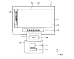
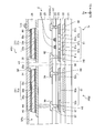
- FIG. 1 is a cross-sectional view showing a schematic cross-sectional configuration of the detection device according to this embodiment.
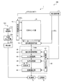
- FIG. 2 is a plan view showing the biological information detecting device according to the present embodiment.
- FIG. 3 is a block diagram showing a schematic configuration example of the detection device according to the present embodiment.
- FIG. 4 is a circuit diagram showing the biological information detecting device.
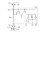
- FIG. 5 is an equivalent circuit diagram showing a partial detection area.
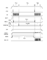
- FIG. 6 is a timing waveform chart showing an operation example of the detection device.
- FIG. 7 is a plan view schematically showing a partial detection area of the biological information detecting device.
- FIG. 8 is a sectional view taken along line VIII-VIII′ of FIG. 7.
- FIG. 9 is a graph schematically showing the relationship between the wavelength and the light absorption coefficient of the first photodiode and the second photodiode.
- FIG. 10 is an equivalent circuit diagram showing a partial detection area according to another example.
- FIG. 11 is a schematic cross-sectional view of a partial detection area according to another example.
- FIG. 12 is a sectional view showing a schematic sectional structure of a switching element included in the drive circuit.
- FIG. 13 is a block diagram of the control unit according to the present embodiment.
- FIG. 14 is a schematic diagram illustrating an example of the locus of the operation position.
- FIG. 15 is a schematic diagram illustrating an example of the locus of the operation position.
- FIG. 16 is a schematic diagram showing an example of user operation.
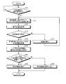
- FIG. 17 is a flowchart illustrating the authentication process according to this embodiment.
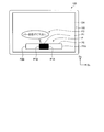
- FIG. 18 is a diagram showing an example of the guide image.
- FIG. 1 is a cross-sectional view showing a schematic cross-sectional configuration of the detection device according to this embodiment.
- the detection device 100 according to the present embodiment is a display device capable of detecting biometric information of a user. As shown in FIG. 1, the detection device 100 includes a biological information detection device 1, a display panel 101, a touch panel 102, and a cover glass 103. The detection device 100 is provided with the biological information detection device 1, a display panel 101, a touch panel 102, and a cover glass 103 so as to overlap with each other.
- the display panel 101 has a plurality of display elements for displaying images.
- an organic EL display panel OLED: Organic Light Emitting Diode
- an inorganic EL display micro LED, Mini
- the display panel 101 is a liquid crystal display panel (LCD: Liquid Crystal Display) using a liquid crystal element as a display element or an electrophoretic display panel (EPD: Electrophoretic Display) using an electrophoretic element as a display element.
- LCD Liquid Crystal Display
- EPD Electrophoretic Display
- the display panel 101 has a first main surface 101a and a second main surface 101b opposite to the first main surface 101a.
- the first main surface 101a is a display surface that displays an image, and irradiates the cover glass 103 with light L1 from the display element of the display panel 101 and the light source unit.
- the first main surface 101a has a display area DA for displaying an image.
- the touch panel 102 is provided on the first main surface 101a of the display panel 101.
- the touch panel 102 is an input unit that receives user operations.
- the touch panel 102 detects a user's finger Fg or palm touching or approaching the surface of the cover glass 103 by, for example, a capacitance method.
- a capacitance method for example, a capacitance method.
- the touch panel 102 has a position sensor unit 10A (see FIG. 3), and the position sensor unit 10A allows the position of the user's finger Fg or the palm close to the surface of the cover glass 103, that is, the finger in the display area DA of the display panel 101.
- the coordinates of the position where Fg and the palm are close to each other are detected.
- the position where the finger Fg or the palm is close in the display area DA of the display panel 101 detected by the position sensor unit 10A is referred to as an operation position.
- the operation position can be restated as a position (coordinates) operated by the user on the touch panel 102.
- the position sensor unit 10A is configured, for example, by providing a plurality of opposed electrodes in a matrix in the display area DA, but the configuration is arbitrary as long as it is a sensor that can detect the operation position.
- the touch panel 102 has translucency and can transmit the light L1 and the reflected light L2.
- the light L2 includes reflected light at the interface between the cover glass 103 and air and reflected light at the surface of the finger Fg.
- the display panel 101 may be integrated with the touch panel 102, or may have the function of the touch panel 102 built therein.
- the cover glass 103 is a member for protecting the display panel 101 and the touch panel 102, and covers the display panel 101 and the touch panel 102.
- the cover glass 103 is, for example, a glass substrate.
- the cover glass 103 is not limited to this, and a resin substrate or the like may be provided on the touch panel 102.
- the surface of the cover glass 103 may be called a detection surface for detecting the finger Fg.
- the biological information detecting device 1 is provided so as to face the second main surface 101b of the display panel 101.
- the display panel 101 is provided between the biological information detecting device 1 and the touch panel 102.
- the biometric information detection device 1 has a biometric sensor unit 10 (see FIG. 3) capable of detecting biometric information. Since the biometric information detection device 1 and the touch panel 102 are provided in an overlapping manner, it can be said that the biometric sensor unit 10 is provided on the touch panel 102 that is an input unit.
- the biometric sensor unit 10 is an optical biometric sensor, for example, a light reflection type biometric information sensor.
- the biometric sensor unit 10 can detect irregularities (for example, fingerprints) on the surface of the finger Fg, the palm or the like by detecting the light L2 reflected at the interface between the cover glass 103 and the air. Further, the biometric sensor unit 10 may detect the blood vessel pattern by detecting the light L2 reflected inside the finger Fg or the palm, or may detect other biometric information. Since it is easy to increase the area of the biometric information detection device 1, the detection area AA of the biometric information detection device 1 is provided so as to face the entire display area DA of the display panel 101.
- the present invention is not limited to this, and the detection area AA may face a part of the display area DA of the display panel 101. Further, the biological information detecting device 1 may be provided between the display panel 101 and the cover glass 103. In this case, the biometric information detection device 1 may be provided between the touch panel 102 and the display panel 101, or the biometric information detection device 1 may have the function of the touch panel incorporated therein.
- FIG. 2 is a plan view showing the biological information detecting device according to the present embodiment.
- the biological information detecting device 1 includes an insulating substrate 21, a biological sensor unit 10, a gate line driving circuit 15, a signal line selecting circuit 16, and an analog front end circuit (hereinafter, AFE (Analog Front). End)) 48, a control circuit 122, and a power supply circuit 123.
- AFE Analog Front
- control board 120 is electrically connected to the insulating board 21 via the flexible printed board 110.
- the flexible printed circuit board 110 is provided with the AFE 48.
- a control circuit 122 and a power supply circuit 123 are provided on the control board 120.
- the control circuit 122 is, for example, an FPGA (Field Programmable Gate Array).
- the control circuit 122 supplies a control signal to the biosensor unit 10, the gate line drive circuit 15, and the signal line selection circuit 16 to control the detection operation of the biosensor unit 10.
- the power supply circuit 123 supplies a voltage signal such as a power supply signal SVS (see FIG. 6) to the biosensor unit 10 and the gate line drive circuit 15.
- the insulating substrate 21 has a detection area AA and a peripheral area GA.
- the detection area AA is an area that overlaps with the plurality of first photodiodes PD1 and the plurality of second photodiodes PD2 (see FIG. 5) of the biological sensor unit 10.
- the peripheral area GA is an area outside the detection area AA, and is an area that does not overlap the first photodiode PD1 and the plurality of second photodiodes PD2. That is, the peripheral area GA is an area between the outer periphery of the detection area AA and the end of the insulating substrate 21.
- the gate line drive circuit 15 and the signal line selection circuit 16 are provided in the peripheral area GA.
- FIG. 3 is a block diagram showing a schematic configuration example of the detection device according to the present embodiment.
- the biological information detection device 1 further includes a detection control unit 11 and a detection unit 40. Some or all of the functions of the detection control unit 11 are included in the control circuit 122. Further, some or all of the functions of the detection unit 40 other than the AFE 48 are included in the control circuit 122.
- the biological sensor unit 10 is an optical sensor having a first photodiode PD1 and a second photodiode PD2 that are photoelectric conversion elements.
- the detection control unit 11 is a circuit that supplies a control signal to each of the gate line drive circuit 15, the signal line selection circuit 16, and the detection unit 40 to control the operation thereof.
- the detection controller 11 supplies various control signals such as a start signal STV, a clock signal CK, and a reset signal RST1 to the gate line drive circuit 15.
- the detection control unit 11 also supplies various control signals such as the selection signal SEL to the signal line selection circuit 16.
- the gate line drive circuit 15 is a circuit that drives a plurality of gate lines GCL (see FIG. 4) based on various control signals.
- the gate line drive circuit 15 sequentially or simultaneously selects a plurality of gate lines GCL and supplies a gate drive signal VGCL to the selected gate line GCL.
- the gate line drive circuit 15 selects the plurality of first photodiodes PD1 and second photodiodes PD2 connected to the gate line GCL.
- the gate line drive circuit 15 is a circuit that drives a plurality of gate lines GCL (see FIG. 4) based on various control signals.
- the gate line drive circuit 15 sequentially or simultaneously selects a plurality of gate lines GCL and supplies a gate drive signal VGCL to the selected gate line GCL.
- the gate line drive circuit 15 selects the plurality of first photodiodes PD1 and second photodiodes PD2 connected to the gate line GCL.
- the signal line selection circuit 16 is a switch circuit that selects a plurality of signal lines SGL (see FIG. 4) sequentially or simultaneously.
- the signal line selection circuit 16 connects the selected signal line SGL to the detection circuit AFE 48 based on the selection signal SEL supplied from the detection control unit 11.
- the signal line selection circuit 16 outputs the detection signal Vdet of the first photodiode PD1 and the second photodiode PD2 to the detection unit 40.
- the signal line selection circuit 16 is, for example, a multiplexer.
- the detection unit 40 is a circuit including an AFE 48, a signal processing unit 44, a coordinate extraction unit 45, a storage unit 46, and a detection timing control unit 47.
- the detection timing control unit 47 controls the AFE 48, the signal processing unit 44, and the coordinate extraction unit 45 to operate in synchronization with each other, based on the control signal supplied from the detection control unit 11.
- the AFE 48 is a signal processing circuit having at least the functions of the detection signal amplifier 42 and the A/D converter 43.
- the detection signal amplifier 42 amplifies the detection signal Vdet.
- the A/D converter 43 converts the analog signal output from the detection signal amplifier 42 into a digital signal.
- the signal processing unit 44 is a logic circuit that detects a predetermined physical quantity input to the biological sensor unit 10 based on the output signal of the AFE 48, that is, the detection signal Vdet converted into a digital signal.
- the signal processing unit 44 detects the surface irregularities (that is, fingerprints) of the finger Fg or the blood vessel pattern of the finger Fg or the palm based on the detection signal Vdet from the AFE 48. it can.
- the storage unit 46 temporarily stores the signal calculated by the signal processing unit 44.
- the storage unit 46 may be, for example, a RAM (Random Access Memory), a register circuit, or the like.
- the coordinate extracting unit 45 is a logic circuit that obtains the detected coordinates of the unevenness of the surface of the finger Fg or the like when the signal processing unit 44 detects the proximity of the finger Fg or the palm.
- the coordinate extracting unit 45 combines the detection signals Vdet output from each of the first photodiode PD1 and the second photodiode PD2 of the biosensor unit 10 to form the shape of the surface unevenness (that is, fingerprint) of the finger Fg or the finger Fg. Two-dimensional information indicating the shape of the blood vessel pattern of the palm or the palm is generated. It can be said that this binary information is the biometric information of the user.
- the coordinate extraction unit 45 may output the detection signal Vdet as the sensor output Vo without calculating the detected coordinates. In this case, the detection signal Vdet may be called biometric information of the user.
- the touch panel 102 also includes a position sensor unit 10A, a detection control unit 11A, and a detection unit 40A.
- the detection control unit 11A is a circuit that drives the position sensor unit 10A.
- the position sensor unit 10A is driven by the detection control unit 11A to output an electronic signal corresponding to the position of the user's finger Fg or the palm near the touch panel 102, that is, the operation position, to the detection unit 40A.
- the detection unit 40A may be a circuit having the same configuration as the detection unit 40.
- the detection unit 40A extracts information on the operation position based on the electric signal from the position sensor unit 10A.
- the detection device 100 has a control unit 6 and a storage unit 8.
- the control unit 6 is an arithmetic device mounted on the detection device 100, that is, a CPU (Central Processing Unit).
- the control unit 6 executes various processes by reading the program from the storage unit 8, for example.
- the storage unit 8 is a memory that stores the calculation contents of the control unit 6 and program information, and is external to, for example, a RAM (Random Access Memory), a ROM (Read Only Memory), and an HDD (Hard Disk Drive). At least one of the storage device is included.
- the detection device 100 is incorporated in an electronic device having a display device, such as a mobile terminal device such as a smartphone, a computer, an automatic teller machine (ATM), and an entrance management device. All or part of the functions of the storage unit 8 and the control unit 6 can be performed by the arithmetic unit and the storage device included in the electronic device.
- the control unit 6 acquires information on the operation position from the detection unit 40A.
- the control unit 6 determines whether the user has operated the touch panel 102 on a predetermined locus based on the acquired operation position.
- the control unit 6 acquires the two-dimensional information created by the coordinate extraction unit 45, that is, the biometric information of the user detected by the biometric sensor unit 10.
- the control unit 6 reads from the storage unit 8 the two-dimensional information stored in advance, that is, the reference biometric information that is the reference biometric information.
- the control unit 6 collates the reference biometric information with the biometric information of the user detected by the biometric sensor unit 10 to determine whether the biometric information of the user detected by the biometric sensor unit 10 matches the reference biometric information. To do. That is, the control unit 6 performs user authentication using the biometric information of the user detected by the biometric sensor unit 10. When the biometric information of the user detected by the biometric sensor unit 10 matches the reference biometric information, the control unit 6 determines that authentication is possible, controls the detection device 100, and executes a predetermined function.
- the predetermined function is, for example, a function requested by the user to be executed by the detection device 100, and examples thereof include activation of a program of the detection device 100, return from a sleep state, and access to a website.
- the control unit 6 When the coordinate extraction unit 45 does not calculate the detected coordinates, the control unit 6 indicates the shape of the unevenness (that is, the fingerprint) of the surface of the finger Fg or the shape of the blood vessel pattern of the finger Fg or the palm from the detection signal Vdet. , Generate two-dimensional information. The detailed control flow of the control unit 6 will be described later.
- FIG. 4 is a circuit diagram showing the biological information detecting device.
- FIG. 5 is an equivalent circuit diagram showing a partial detection area.
- FIG. 6 is a timing waveform chart showing an operation example of the biological information detecting device.
- the biometric sensor unit 10 has a plurality of partial detection areas PAA arranged in a matrix.
- the partial detection area PAA includes a first photodiode PD1 and a second photodiode PD2, a capacitive element Ca, and a first switching element Tr.
- the first switching element Tr is provided corresponding to the first photodiode PD1 and the second photodiode PD2.
- the first switching element Tr is composed of a thin film transistor, and in this example, is composed of an n-channel type TFT (Thin Film Transistor).
- the gate of the first switching element Tr is connected to the gate line GCL.
- the source of the first switching element Tr is connected to the signal line SGL.
- the drain of the first switching element Tr is connected to the cathode electrode 34 of the first photodiode PD1, the cathode electrode 54 of the second photodiode PD2, and one end of the capacitive element Ca.
- the anode electrode 35 of the first photodiode PD1, the anode electrode 55 of the second photodiode PD2, and the other end of the capacitive element Ca are connected to a reference potential, for example, the ground potential.
- the first photodiode PD1 and the second photodiode PD2 are connected in parallel to the first switching element Tr in the same direction.
- the third switching element TrS and the fourth switching element TrR are connected to the signal line SGL.
- the third switching element TrS and the fourth switching element TrR are elements that form a drive circuit that drives the first switching element Tr.
- the drive circuit includes the gate line drive circuit 15, the signal line selection circuit 16, the reset circuit 17 and the like provided in the peripheral area GA.
- the third switching element TrS is composed of, for example, a CMOS (complementary MOS) transistor in which a p-channel transistor p-TrS and an n-channel transistor n-TrS are combined.
- the fourth switching element TrR is also composed of a CMOS transistor.
- the power supply circuit 123 supplies the reference signal VR1 which is the initial potential of the capacitance element Ca to the capacitance element Ca.
- the capacitive element Ca is reset.
- the partial detection area PAA is irradiated with light
- a current corresponding to the amount of light flows in each of the first photodiode PD1 and the second photodiode PD2, whereby charges are accumulated in the capacitive element Ca.
- the first switching element Tr is turned on, a current flows through the signal line SGL according to the electric charge accumulated in the capacitive element Ca.
- the signal line SGL is connected to the AFE 48 via the third switching element TrS of the signal line selection circuit 16.
- the biological information detecting device 1 can detect a signal corresponding to the light amount of the light with which the first photodiode PD1 and the second photodiode PD2 are irradiated, for each partial detection area PAA.
- the gate line GCL extends in the first direction Dx and is connected to the plurality of partial detection areas PAA arranged in the first direction Dx. Further, the plurality of gate lines GCL1, GCL2,..., GCL8 are arranged in the second direction Dy and are connected to the gate line drive circuit 15, respectively.
- the gate lines GCL1, GCL2,..., GCL8 are simply referred to as the gate lines GCL unless it is necessary to distinguish them.
- the number of gate lines GCL is eight, but this is merely an example, and eight or more gate lines GCL may be arranged, for example, 256.
- the first direction Dx is one direction in a plane parallel to the insulating substrate 21, for example, a direction parallel to the gate line GCL.
- the second direction Dy is one direction in a plane parallel to the insulating substrate 21 and is a direction orthogonal to the first direction Dx.
- the second direction Dy may intersect with the first direction Dx instead of intersecting at right angles.
- the third direction Dz is a direction orthogonal to the first direction Dx and the second direction Dy, and is a direction perpendicular to the insulating substrate 21.
- the signal line SGL extends in the second direction Dy and is connected to the plurality of partial detection areas PAA arranged in the second direction Dy.
- the plurality of signal lines SGL1, SGL2,..., SGL12 are arranged in the first direction Dx and are connected to the signal line selection circuit 16 and the reset circuit 17, respectively.
- the number of the signal lines SGL is 12, but this is merely an example, and the signal lines SGL may be arranged in 12 or more, for example, 252.
- the biological sensor unit 10 is provided between the signal line selection circuit 16 and the reset circuit 17. The configuration is not limited to this, and the signal line selection circuit 16 and the reset circuit 17 may be connected to the ends of the signal line SGL in the same direction.
- the gate line drive circuit 15 receives various control signals such as a start signal STV, a clock signal CK, and a reset signal RST1 via the level shifter 151.
- the gate line drive circuit 15 has a plurality of second switching elements TrG (not shown).
- the gate line driving circuit 15 sequentially selects the plurality of gate lines GCL1, GCL2,..., GCL8 in a time division manner by the operation of the second switching element TrG.
- the gate line drive circuit 15 supplies the gate drive signal VGCL to the plurality of first switching elements Tr via the selected gate line GCL.
- the plurality of partial detection areas PAA arranged in the first direction Dx are selected as detection targets.
- the signal line selection circuit 16 has a plurality of selection signal lines Lsel, a plurality of output signal lines Lout, and a third switching element TrS.
- the plurality of third switching elements TrS are provided corresponding to the plurality of signal lines SGL, respectively.
- the six signal lines SGL1, SGL2,..., SGL6 are connected to a common output signal line Lout1.
- the six signal lines SGL7, SGL8,..., SGL12 are connected to a common output signal line Lout2.
- the output signal lines Lout1 and Lout2 are connected to the AFE 48, respectively.
- the signal lines SGL1, SGL2,..., SGL6 are the first signal line blocks
- the signal lines SGL7, SGL8,..., SGL12 are the second signal line blocks.
- the plurality of selection signal lines Lsel are respectively connected to the gates of the third switching elements TrS included in one signal line block. Further, one selection signal line Lsel is connected to the gates of the third switching elements TrS of the plurality of signal line blocks.
- the selection signal lines Lsel1, Lsel2,..., Lsel6 are connected to the third switching elements TrS corresponding to the signal lines SGL1, SGL2,..., SGL6.
- the selection signal line Lsel1 is connected to the third switching element TrS corresponding to the signal line SGL1 and the third switching element TrS corresponding to the signal line SGL7.
- the selection signal line Lsel2 is connected to the third switching element TrS corresponding to the signal line SGL2 and the third switching element TrS corresponding to the signal line SGL8.
- the control circuit 122 (see FIG. 2) sequentially supplies the selection signal SEL to the selection signal line Lsel via the level shifter 161.
- the signal line selection circuit 16 sequentially selects the signal lines SGL in one signal line block in a time division manner by the operation of the third switching element TrS. Further, the signal line selection circuit 16 simultaneously selects the signal lines SGL one by one in the plurality of signal line blocks.
- the biological information detecting device 1 can reduce the number of ICs (Integrated Circuits) including the AFE 48 or the number of IC terminals.
- the reset circuit 17 has a reference signal line Lvr, a reset signal line Lrst, and a fourth switching element TrR.
- the fourth switching element TrR is provided corresponding to the plurality of signal lines SGL.
- the reference signal line Lvr is connected to one of the source and the drain of the plurality of fourth switching elements TrR.
- the reset signal line Lrst is connected to the gates of the plurality of fourth switching elements TrR.
- the control circuit 122 supplies the reset signal RST2 to the reset signal line Lrst via the level shifter 171. As a result, the plurality of fourth switching elements TrR are turned on, and the plurality of signal lines SGL are electrically connected to the reference signal line Lvr.
- the power supply circuit 123 supplies the reference signal VR1 to the reference signal line Lvr. As a result, the reference signal VR1 is supplied to the capacitive element Ca included in the plurality of partial detection areas PAA.
- the biological information detection device 1 has a reset period Prst, an exposure period Pex, and a read period Pdet.
- the power supply circuit 123 supplies the power supply signal SVS to the first photodiode PD1 and the second photodiode PD2 over the reset period Prst, the exposure period Pex, and the read period Pdet.
- the control circuit 122 supplies the reference signal VR1 and the reset signal RST2, which are high-level voltage signals, to the reset circuit 17 at a time before the reset period Prst starts.
- the control circuit 122 supplies the start signal STV to the gate line drive circuit 15, and the reset period Prst starts.
- the gate line drive circuit 15 sequentially selects the gate line GCL based on the start signal STV, the clock signal CK, and the reset signal RST1.
- the gate line drive circuit 15 sequentially supplies the gate drive signal VGCL to the gate line GCL.
- the gate drive signal VGCL has a pulsed waveform having a high level voltage VGH and a low level voltage VGL.
- 256 gate lines GCL are provided, and the gate drive signals VGCL1,..., VGCL256 are sequentially supplied to each gate line GCL.
- the capacitive elements Ca in all the partial detection areas PAA are sequentially electrically connected to the signal line SGL and the reference signal VR1 is supplied.
- the capacitance of the capacitive element Ca is reset.
- the exposure period Pex starts after the gate drive signal VGCL 256 is supplied to the gate line GCL.
- the actual exposure periods Pex1,..., Pex256 in the partial detection area PAA corresponding to each gate line GCL have different start timings and end timings.
- the exposure periods Pex1,..., Pex256 are started at the timing when the gate drive signal VGCL changes from the high level voltage VGH to the low level voltage VGL in the reset period Prst.
- the exposure periods Pex1,..., Pex256 are ended at the timing when the gate drive signal VGCL changes from the low level voltage VGL to the high level voltage VGH in the read period Pdet.
- the exposure time lengths of the exposure periods Pex1,..., Pex256 are equal.
- the control circuit 122 sets the reset signal RST2 to a low level voltage at the timing before the read period Pdet starts. As a result, the operation of the reset circuit 17 is stopped.
- the gate line drive circuit 15 sequentially supplies the gate drive signals VGCL1,..., VGCL256 to the gate line GCL.
- the control circuit 122 sequentially supplies the selection signals SEL1,..., SEL6 to the signal line selection circuit 16 while the gate drive signal VGCL1 is at the high level voltage VGH.
- the signal lines SGL in the partial detection area PAA selected by the gate drive signal VGCL1 are connected to the AFE 48 sequentially or simultaneously.
- the detection signal Vdet is supplied to the AFE 48.
- the signal line selection circuit 16 sequentially selects the signal line SGL in each period in which each gate drive signal VGCL becomes the high level voltage VGH.
- the biometric information detection device 1 can output the detection signal Vdet of all the partial detection areas PAA to the AFE 48 during the read period Pdet.
- the biological information detecting device 1 may perform detection by repeatedly executing the reset period Prst, the exposure period Pex, and the read period Pdet. Alternatively, the biological information detection apparatus 1 may start the detection operation at the timing when it is detected that the finger Fg or the like is in contact with or in proximity to the detection surface.
- FIG. 7 is a plan view schematically showing a partial detection area of the biological information detecting device.
- FIG. 8 is a sectional view taken along line VIII-VIII′ of FIG. 7. Note that, in FIG. 7, the cathode electrode 34 and the anode electrode 35 are indicated by a chain double-dashed line in order to make the drawing easy to see.
- the direction from the insulating substrate 21 to the first photodiode PD1 in the direction perpendicular to the surface of the insulating substrate 21 is referred to as “upper” or simply “upper”.
- the direction from the first photodiode PD1 to the insulating substrate 21 is “lower side” or simply “lower”.
- the “plan view” refers to a case viewed from a direction perpendicular to the surface of the insulating substrate 21.
- the partial detection area PAA is an area surrounded by a plurality of gate lines GCL and a plurality of signal lines SGL.
- the first photodiode PD1, the second photodiode PD2, and the first switching element Tr are provided in the partial detection area PAA, that is, in the area surrounded by the plurality of gate lines GCL and the plurality of signal lines SGL.
- the first photodiode PD1 and the second photodiode PD2 are, for example, PIN (Positive Intrinsic Negative Diode) type photodiodes.
- the first photodiode PD1 includes a first semiconductor layer 31, a cathode electrode 34, and an anode electrode 35.
- the first semiconductor layer 31 includes a first partial semiconductor layer 31a and a second partial semiconductor layer 31b.
- the first partial semiconductor layer 31a and the second partial semiconductor layer 31b of the first photodiode PD1 are amorphous silicon (a-Si).
- the first partial semiconductor layer 31a and the second partial semiconductor layer 31b are provided adjacent to each other with a spacing SP in the first direction Dx.
- the cathode electrode 34 and the anode electrode 35 are continuously provided over a region overlapping with the first partial semiconductor layer 31a, the second partial semiconductor layer 31b, and the space SP.
- the first semiconductor layer 31 when it is not necessary to distinguish between the first partial semiconductor layer 31a and the second partial semiconductor layer 31b, they may be simply referred to as the first semiconductor layer 31.
- the first photodiode PD1 is provided so as to overlap the second photodiode PD2. Specifically, the first partial semiconductor layer 31a of the first photodiode PD1 overlaps the second photodiode PD2.
- the second photodiode PD2 includes a second semiconductor layer 51, a cathode electrode 54, and an anode electrode 55.
- the second semiconductor layer 51 is polysilicon. More preferably, the second semiconductor layer 51 is low temperature polysilicon (hereinafter referred to as LTPS (Low Temperature Polycrystalline Silicon)).
- the second semiconductor layer 51 has an i region 52a, ap region 52b, and an n region 52c.
- i region 52a is arranged between p region 52b and n region 52c.
- the p region 52b, the i region 52a, and the n region 52c are arranged in this order.
- polysilicon is doped with impurities to form an n+ region.
- p region 52b polysilicon is doped with impurities to form ap+ region.
- the i region 52a is, for example, a non-doped intrinsic semiconductor and has a lower conductivity than the p region 52b and the n region 52c.
- the second semiconductor layer 51 and the first partial semiconductor layer 31a of the first photodiode PD1 are connected via the first relay electrode 56 and the second relay electrode 57.
- the portion of the first relay electrode 56 that overlaps the second semiconductor layer 51 functions as the cathode electrode 54.
- a portion of the second relay electrode 57 that overlaps the second semiconductor layer 51 functions as the anode electrode 55.
- the first switching element Tr is provided in a region overlapping the second partial semiconductor layer 31b of the first photodiode PD1.
- the first switching element Tr has a third semiconductor layer 61, a source electrode 62, a drain electrode 63, and a gate electrode 64.
- the third semiconductor layer 61 is polysilicon like the second semiconductor layer 51. More preferably, the third semiconductor layer 61 is LTPS.
- the portion of the first relay electrode 56 that overlaps the third semiconductor layer 61 functions as the source electrode 62.
- a portion of the signal line SGL that overlaps with the third semiconductor layer 61 functions as the drain electrode 63.
- the gate electrode 64 branches from the gate line GCL in the second direction Dy and overlaps with the third semiconductor layer 61.
- the two gate electrodes 64 have a so-called double gate structure provided so as to overlap the third semiconductor layer 61.
- the first switching element Tr is connected to the cathode electrode 34 of the first photodiode PD1 and the cathode electrode 54 of the second photodiode PD2 via the first relay electrode 56.
- the first switching element Tr is also connected to the signal line SGL.
- the first switching element Tr is provided on the insulating substrate 21.
- the insulating substrate 21 is, for example, a translucent glass substrate.
- the insulating substrate 21 may be a resin substrate or a resin film made of a resin having translucency such as polyimide.
- the biological information detecting device 1 the first photodiode PD1, the second photodiode PD2, and the first switching element Tr are formed on the insulating substrate 21. Therefore, as compared with the case where a semiconductor substrate such as a silicon substrate is used, for example, the biological information detecting device 1 can easily increase the area of the detection area AA.
- Light-shielding layers 67 and 68 are provided on the insulating substrate 21.
- the undercoat film 22 covers the light shielding layers 67 and 68, and is provided on the insulating substrate 21.
- the undercoat film 22, the gate insulating film 23, and the first interlayer insulating film 24 are inorganic insulating films, and a silicon oxide film (SiO), a silicon nitride film (SiN), a silicon oxynitride film (SiON), or the like is used. Further, each inorganic insulating film is not limited to a single layer and may be a laminated film.
- the second semiconductor layer 51 and the third semiconductor layer 61 are provided on the undercoat film 22. That is, the second semiconductor layer 51 of the second photodiode PD2 and the third semiconductor layer 61 of the first switching element Tr are provided in the same layer. Further, the light shielding layer 67 is provided between the second semiconductor layer 51 and the insulating substrate 21 in the third direction Dz. As a result, it is possible to prevent the light L1 from being directly applied to the second photodiode PD2. Further, the light shielding layer 68 is provided between the third semiconductor layer 61 and the insulating substrate 21 in the third direction Dz. Thereby, the light leak current of the first switching element Tr can be suppressed.
- the third semiconductor layer 61 includes an i region 61a, an LDD (Lightly Doped Drain) region 61b, and an n region 61c.
- the i region 61a is formed in a region overlapping with the gate electrode 64, respectively.
- the n region 61c is a high-concentration impurity region and is formed in a region connected to the source electrode 62 and the drain electrode 63.
- the LDD region 61b is a low-concentration impurity region and is formed between the n region 61c and the i region 61a and between the two i regions 61a.
- the gate insulating film 23 is provided on the undercoat film 22 so as to cover the second semiconductor layer 51 and the third semiconductor layer 61.
- the gate electrode 64 is provided on the gate insulating film 23. That is, the first switching element Tr has a so-called top gate structure in which the gate electrode 64 is provided on the upper side of the third semiconductor layer 61. However, the first switching element Tr may have a so-called dual gate structure in which the gate electrode 64 is provided on both the upper side and the lower side of the third semiconductor layer 61, or the gate electrode 64 may be the third semiconductor layer 61. It may be a bottom gate structure provided on the lower side.
- the first interlayer insulating film 24 is provided on the gate insulating film 23 so as to cover the gate electrode 64.
- the first interlayer insulating film 24 is also provided on the upper side of the second semiconductor layer 51.
- the first relay electrode 56, the second relay electrode 57, and the signal line SGL are provided on the first interlayer insulating film 24.
- the source electrode 62 (first relay electrode 56) is connected to the third semiconductor layer 61 via the contact hole H8.
- the drain electrode 63 (signal line SGL) is connected to the third semiconductor layer 61 via the contact hole H7.
- the cathode electrode 54 (first relay electrode 56) is connected to the n region 52c of the second semiconductor layer 51 via the contact hole H6.
- the cathode electrode 54 of the second photodiode PD2 is connected to the first switching element Tr.
- the anode electrode 55 (second relay electrode 57) is connected to the p region 52b of the second semiconductor layer 51 via the contact hole H5.
- the second interlayer insulating film 25 is provided on the first interlayer insulating film 24 so as to cover the second photodiode PD2 and the first switching element Tr.
- the second interlayer insulating film 25 is an organic film, and is a flattening film that flattens unevenness formed by various conductive layers.
- the second interlayer insulating film 25 may be formed of the above-mentioned inorganic material.
- the anode electrode 35 of the first photodiode PD1 is provided on the second interlayer insulating film 25 of the backplane 2.
- the backplane 2 is a drive circuit board that drives the sensor for each predetermined detection area.
- the backplane 2 includes an insulating substrate 21, a first switching element Tr, a second switching element TrG provided on the insulating substrate 21, various wirings, and the like.
- the first partial semiconductor layer 31a includes an i-type semiconductor layer 32a, a p-type semiconductor layer 32b, and an n-type semiconductor layer 32c.
- the second partial semiconductor layer 31b includes an i-type semiconductor layer 33a, a p-type semiconductor layer 33b and an n-type semiconductor layer 33c.
- the i-type semiconductor layers 32a and 33a, the p-type semiconductor layers 32b and 33b, and the n-type semiconductor layers 32c and 33c are specific examples of photoelectric conversion elements. In FIG.
- the i-type semiconductor layers 32a and 33a are provided between the p-type semiconductor layers 32b and 33b and the n-type semiconductor layers 32c and 33c.
- the p-type semiconductor layers 32b and 33b, the i-type semiconductor layers 32a and 33a, and the n-type semiconductor layers 32c and 33c are sequentially stacked on the anode electrode 35.
- the n-type semiconductor layers 32c and 33c form an n+ region by doping a-Si with impurities.
- a-Si is doped with impurities to form p+ regions.
- the i-type semiconductor layers 32a and 33a are, for example, non-doped intrinsic semiconductors and have lower conductivity than the n-type semiconductor layers 32c and 33c and the p-type semiconductor layers 32b and 33b.
- the cathode electrode 34 and the anode electrode 35 are a light-transmitting conductive material such as ITO (Indium Tin Oxide).
- the cathode electrode 34 is an electrode for supplying the power supply signal SVS to the photoelectric conversion layer.
- the anode electrode 35 is an electrode for reading the detection signal Vdet.
- the anode electrode 35 is provided on the second interlayer insulating film 25.
- the anode electrode 35 is continuously provided over the first partial semiconductor layer 31a and the second partial semiconductor layer 31b.
- the anode electrode 35 is connected to the second relay electrode 57 via a contact hole H4 provided in the second interlayer insulating film 25.
- a third interlayer insulating film 26 is provided so as to cover the first partial semiconductor layer 31a and the second partial semiconductor layer 31b.
- the third interlayer insulating film 26 is an organic film, and is a flattening film that flattens the unevenness formed by the first partial semiconductor layer 31a and the second partial semiconductor layer 31b.
- the cathode electrode 34 is provided on the third interlayer insulating film 26.
- the cathode electrode 34 is continuously provided on the first partial semiconductor layer 31a and the second partial semiconductor layer 31b.
- the cathode electrode 34 is connected to the first partial semiconductor layer 31a and the second partial semiconductor layer 31b through the contact holes H2 and H1 provided in the third interlayer insulating film 26. Thereby, the first partial semiconductor layer 31a and the second partial semiconductor layer 31b are connected in parallel between the anode electrode 35 and the cathode electrode 34, and function as one photoelectric conversion element.
- the cathode electrode 34 is connected to the first relay electrode 56 via the contact hole H3 at the interval SP between the first partial semiconductor layer 31a and the second partial semiconductor layer 31b.
- the contact hole H3 is a through hole penetrating the second interlayer insulating film 25 and the third interlayer insulating film 26 in the third direction Dz.
- An opening 35a is provided in a portion of the anode electrode 35 overlapping the contact hole H3, and the contact hole H3 is formed through the opening 35a.
- the capacitance of the capacitive element Ca shown in FIG. 5 is formed between the anode electrode 55 and the cathode electrode 34 facing each other with the third interlayer insulating film 26 in between at the interval SP.
- it is formed between the anode electrode 55 and the cathode electrode 34 facing each other with the third interlayer insulating film 26 interposed therebetween at the interval SPa around the periphery of the first photodiode PD1. Positive charges are held in the capacitor Ca during the exposure period Pex.
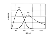
- FIG. 9 is a graph schematically showing the relationship between the wavelength and the light absorption coefficient of the first photodiode and the second photodiode.
- the horizontal axis of FIG. 9 represents the wavelength, and the vertical axis represents the light absorption coefficient.
- the light absorption coefficient is an optical constant indicating the degree of absorption of light traveling in a substance.
- the first photodiode PD1 containing a-Si exhibits a good light absorption coefficient in the visible light region, for example, the wavelength region of 300 nm or more and 800 nm or less.
- the second photodiode PD2 including polysilicon exhibits a good light absorption coefficient in a region including a visible light region to an infrared region, for example, a wavelength region of 500 nm or more and 1100 nm or less.
- the first photodiode PD1 has high sensitivity in the visible light region
- the second photodiode PD2 has high sensitivity in the red wavelength region, which is a different wavelength region from the first photodiode PD1, to the infrared region.
- the biometric information detection device 1 of the present embodiment has a stack of a first photodiode PD1 and a second photodiode PD2 having different sensitivity wavelength regions. Therefore, the wavelength region having sensitivity can be widened as compared with the configuration including either one of the photodiodes.
- the light L1 passes through the biological information detecting device 1 through the space SP and the space SPa.
- the light L2 (see FIG. 1) reflected by the finger Fg enters the first photodiode PD1.
- the first photodiode PD1 can favorably detect blue or green light L2.
- the infrared light L2 is not absorbed by the first photodiode PD1 and is incident on the second photodiode PD2.
- the second photodiode PD2 can satisfactorily detect the infrared light L2.
- the biological information detecting apparatus 1 can detect information on various biological bodies with the same device (biological information detecting apparatus 1).
- the biological information detecting device 1 can improve the photosensitivity.
- the first photodiode PD1 and the second photodiode PD2 are provided in the partial detection area PAA, that is, in the area surrounded by the plurality of gate lines GCL and the plurality of signal lines SGL. According to this, the number of switching elements and the number of wirings are reduced as compared with the case where the first switching element Tr, the gate line GCL, and the signal line SGL are provided in each of the first photodiode PD1 and the second photodiode PD2. can do. Therefore, the biological information detecting apparatus 1 can improve the detection resolution.
- the biosensor unit 10 has the first photodiode PD1 having the first semiconductor layer 31 containing amorphous silicon and the second photodiode PD2 having the second semiconductor layer 51 containing polysilicon. Then, in the biosensor unit 10, the first semiconductor layer 31 containing amorphous silicon and the second semiconductor layer 51 containing polysilicon, that is, the first photodiode PD1 and the second photodiode PD2 are arranged in the third direction Dz. They are stacked so that they overlap. However, in the biosensor unit 10, the first photodiode PD1 and the second photodiode PD2 may not be stacked in the third direction Dz, and may be provided in the same layer, for example.
- the biometric sensor unit 10 can detect the fingerprint of the user with the first photodiode PD1 and the blood vessel pattern of the user with the second photodiode PD2 as the biometric information.
- the blood vessel pattern refers to an image of blood vessels, and is a vein pattern in the present embodiment.
- the biometric sensor unit 10 detects the fingerprint and the blood vessel pattern as the biometric information of the user, it may detect at least one of the fingerprint and the blood vessel pattern.
- the biometric sensor unit 10 may be one that detects biometric information other than the fingerprint and the blood vessel pattern (for example, pulse, pulse wave, etc.).
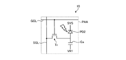
- FIG. 10 is an equivalent circuit diagram showing a partial detection area according to another example.
- the biosensor unit 10 in this example has a plurality of partial detection areas PAA arranged in a matrix.
- the partial detection area PAA of the biological sensor unit 10 includes a second photodiode PD2, a capacitive element Ca, and a first switching element Tr.
- the first switching element Tr is provided corresponding to the second photodiode PD2.
- the gate of the first switching element Tr is connected to the gate line GCL.
- the source of the first switching element Tr is connected to the signal line SGL.
- the drain of the first switching element Tr is connected to the cathode electrode 54 of the second photodiode PD2 and one end of the capacitive element Ca.
- the anode electrode 55 of the second photodiode PD2 and the other end of the capacitive element Ca are connected to a reference potential, for example, the ground potential. That is, the biological sensor unit 10 does not include the first photodiode PD1.
- FIG. 11 is a schematic cross-sectional view of a partial detection area according to another example.
- the first switching element Tr is provided on the insulating substrate 21 as in the case of FIG. 8.
- the biological sensor unit 10 in this example is not provided with the first photodiode PD1 unlike FIG. 8.
- the biological sensor unit 10 in this example is different from that in FIG. 8 in the position where the second photodiode PD2 is provided.
- the second photodiode PD2 is provided above the first switching element Tr, that is, on the third direction Dz side.
- the anode electrode 35 of the second photodiode PD2 is provided on the second interlayer insulating film 25.
- the anode electrode 35, the second semiconductor layer 51, and the cathode electrode 34 are stacked in this order.
- the second semiconductor layer 51 is laminated on the anode electrode 35 in the order of a p region 52b, an i region 52a, and an n region 52c.
- the anode electrode 35 is connected to the source electrode 62 of the first switching element Tr via a contact hole H4 provided in the second interlayer insulating film 25.
- the biosensor unit 10 may include the second photodiode PD2 having the second semiconductor layer 51 containing polysilicon and may not include the first photodiode PD1 as described above. In this case, since the biosensor unit 10 includes the second photodiode PD2, it is possible to preferably detect the blood vessel pattern of the user.
- the biometric sensor unit 10 When the biometric sensor unit 10 is a sensor that detects the user's fingerprint and does not detect the user's blood vessel pattern, the biometric sensor unit 10 does not include the second photodiode PD2 but includes the first photodiode PD1. In that case, the equivalent circuit of the biosensor unit 10 is obtained by replacing the second photodiode PD2 of FIG. 10 with the first photodiode PD1, and the laminated configuration of the biosensor unit 10 is the second photodiode PD2 of FIG. Is preferably replaced with the first photodiode PD1.
- the laminated structure of the biometric sensor unit 10 has been described above, the biometric sensor unit 10 is not limited to the above description and may have any structure as long as it can detect biometric information of the user.
- FIG. 12 is a sectional view showing a schematic sectional structure of a switching element included in the drive circuit.
- FIG. 12 illustrates the third switching element TrS included in the signal line selection circuit 16 as a drive circuit switching element.
- the description of FIG. 12 can be applied to a switching element included in another drive circuit. That is, the second switching element TrG included in the gate line drive circuit 15 and the fourth switching element TrR included in the reset circuit 17 can also have the same configuration as in FIG.
- the n-channel transistor n-TrS of the third switching element TrS includes a fourth semiconductor layer 71, a source electrode 72, a drain electrode 73 and a gate electrode 74.
- the p-channel transistor p-TrS includes a fifth semiconductor layer 81, a source electrode 82, a drain electrode 83 and a gate electrode 84.
- a light shielding layer 75 is provided between the fourth semiconductor layer 71 and the insulating substrate 21, and a light shielding layer 85 is provided between the fifth semiconductor layer 81 and the insulating substrate 21.
- the fourth semiconductor layer 71 and the fifth semiconductor layer 81 are both polysilicon. More preferably, the fourth semiconductor layer 71 and the fifth semiconductor layer 81 are LTPS.
- the fourth semiconductor layer 71 includes an i region 71a, an LDD region 71b, and an n region 61c.
- the fifth semiconductor layer 81 also includes an i region 81a and a p region 81b.
- the layer structure of the n-channel transistor n-TrS and the p-channel transistor p-TrS is the same as that of the first switching element Tr shown in FIG. That is, the fourth semiconductor layer 71 and the fifth semiconductor layer 81 are provided in the same layer as the second semiconductor layer 51 and the third semiconductor layer 61 shown in FIG.
- the gate electrode 74 and the gate electrode 84 are provided in the same layer as the gate electrode 64 shown in FIG.
- the source electrode 72, the drain electrode 73, the source electrode 82, and the drain electrode 83 are provided in the same layer as the source electrode 62 (first relay electrode 56) and the drain electrode 63 (signal line SGL) shown in FIG.
- the first photodiode PD1 and the first switching element Tr provided in the detection area AA and the switching elements such as the third switching element TrS provided in the peripheral area GA are formed of the same material in the same layer. It is provided. This simplifies the manufacturing process of the biological information detecting device 1 and suppresses the manufacturing cost.
- the drive circuit provided in the peripheral area GA is not limited to the CMOS transistor, and may be configured by either the n-channel transistor n-TrS or the p-channel transistor p-TrS.
- the detection device 100 is configured as described above. Next, a method of authenticating a user by the control unit 6 will be described.
- FIG. 13 is a block diagram of the control unit according to this embodiment.
- the control unit 6 includes an operation position acquisition unit 160, an operation determination unit 162, a biometric information acquisition unit 164, an authentication unit 166, and a function control unit 168.
- the operation position acquisition unit 160, the operation determination unit 162, the biometric information acquisition unit 164, the authentication unit 166, and the function control unit 168 are realized by the control unit 6 reading software (program) from the storage unit 8. Then, the processing described later is executed.
- the operation position acquisition unit 160 acquires an operation position which is a position operated by the user on the touch panel 102.
- the operation position is detected by the position sensor unit 10A as described above.
- the operation position acquisition unit 160 acquires operation position information from the position sensor unit 10A.
- the operation position acquisition unit 160 acquires information on the operation position for each predetermined time, that is, information on the proximity position of the user's finger Fg or palm for each predetermined time.
- the detection of the operation position may be performed by the coordinate extraction unit 45 of the detection unit 40 of the biological information acquisition device.
- the operation determination unit 162 determines whether the user has operated the touch panel 102 on a predetermined locus based on the operation position detected by the position sensor unit 10A, that is, the operation position acquired by the operation position acquisition unit 160.
- the locus here means a locus along which the operation position moves when the operation position, that is, the position on the touch panel 102 where the user brings the finger Fg or the palm close to each other continuously moves with the passage of time. ..
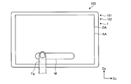
- FIG. 14 is a schematic diagram illustrating an example of the locus of the operation position. As shown in the example of FIG. 14, the trajectory M of the operation position continuously moves on the touch panel 102, that is, on the display area DA and the display area DA that are overlapped on the surface of the touch panel 102 with the passage of time. It has a predetermined length obtained by tracing the operation position. Of course, the trajectory M of the operation position may be detected by the coordinate extraction unit 45 of the detection unit 40 of the biological information acquisition device.
- the operation determination unit 162 determines whether the operation position continuously moves according to the passage of time, that is, whether the operation position draws a locus M, and the locus M is a predetermined locus. To determine if In the present embodiment, the trajectory M when the operation position moves in a plurality of directions that are different from each other over time is set as the predetermined trajectory. That is, when the operation position continuously moves in a plurality of directions different from each other over time, the operation determination unit 162 draws a predetermined trajectory, and the user moves the touch panel 102 along the predetermined trajectory. Judge that you operated.
- the operation determination unit 162 does not draw the predetermined path, and the user touches the touch panel with the predetermined path. It is determined that 102 is not operated.
- the pinch-out operation corresponds to this operation, that is, the operation of the touch panel 102 on a predetermined locus.
- the display device is not limited to displaying a predetermined locus and operating the user along the predetermined locus, and may only instruct a predetermined motion such as a pinch-out motion or a sliding motion.
- FIG. 15 is a schematic diagram illustrating an example of a locus of operation positions.
- FIG. 15 illustrates an example of a case where the operation position continuously moves in a plurality of directions that are different from each other with the passage of time.
- the operation positions at the first time T1 are the operation positions M1A and M1B.
- the operation positions at the second time T2 after the first time T1 are the operation positions M2A and M2B.
- the operation position M2A is on the direction DA side with respect to the operation position M1A.
- the operation position M2B is on the direction DB side in a direction different from the direction DA with respect to the operation position M1B.
- the operation positions at the third time T3 after the second time T2 are the operation positions M3A and M3B.
- the operation position M3A is on the direction DA side with respect to the operation position M2A.
- the operation position M3B is on the direction DB side in a direction different from the direction DA with respect to the operation position M2B.
- the locus M of the operation position is the direction DA moving from the operation position M1A to the operation position M2A to the operation position M3A, and the direction DB′ moving from the operation position M1B to the operation position M2B to the operation position M3B.
- the operation positions are moved in mutually different directions.
- the operation determination unit 162 determines that the operation position draws a predetermined trajectory when the operation position is moving as shown in FIG. 15, for example.
- FIG. 15 is an example of the predetermined trajectory
- the operation determination unit 162 in the present embodiment determines that the operation position draws the predetermined trajectory when the operation positions continuously move in different directions. do it.
- the operation position M1A, the operation position M2A, and the operation position M3A are continuously moved in the same direction DA, but the movement direction may change over time. Good.
- the operation position is moving in a plurality of different directions at the same timing (for example, the direction from the operation position M1A to the operation position M2A and the direction from the operation position M1B to the operation position M2B). It is only necessary to determine that the predetermined position is drawn. Further, in the example of FIG. 15, the operation position is moved in two different directions at the same timing, but the operation position may be moved in three or more different directions.
- the predetermined locus is not limited to the one in which the operation position continuously moves in a plurality of directions that are different from each other over time, and can be set arbitrarily.
- the predetermined locus indicates that the operation position is continuously moving for a predetermined length or more over time (for example, as shown in FIG. 14, the user slides on the screen with at least one finger Fg. It may be determined that a predetermined trajectory is drawn.
- the biometric information acquisition unit 164 acquires biometric information (for example, fingerprint and blood vessel pattern) of the user from the biometric sensor unit 10. Specifically, as described above, the biological sensor unit 10 outputs the detection signal Vdet corresponding to the light L2 reflected by the user's finger Fg or the palm which is in proximity to the touch panel 102 to the signal line selection circuit 16 (FIG. 3)) to the detection unit 40 (see FIG. 3). Then, the detection unit 40 causes the coordinate extraction unit 45 to generate biometric information of the user (here, two-dimensional information of a fingerprint or a blood vessel pattern) based on the detection signal Vdet. The biometric information acquisition unit 164 acquires the biometric information of the user from the detection unit 40.
- biometric information for example, fingerprint and blood vessel pattern
- the biometric information acquisition unit 164 acquires the biometric information of the user at the operation position on which the predetermined trajectory is drawn.
- the biometric information acquisition unit 164 uses the biosensor unit 10 to operate the touch panel 102 on the predetermined trajectory. To obtain biometric information of the user. That is, the biometric information acquisition unit 164 acquires, from the biometric sensor unit 10, biometric information of the user at the operation position on which the predetermined trajectory is drawn at the timing when the predetermined trajectory is drawn.
- the biometric information acquisition unit 164 may acquire biometric information of the user at all operation positions of the plurality of operation positions that draw a predetermined trajectory, or may acquire biometric information of the user at some operation positions. May be.
- the biometric information acquisition unit 164 may acquire the biometric information of the operation position on the side where the detected time is later. That is, in the example of FIG. 15, of the operation positions M1A, M1B, M2A, M2B, M3A, M3B, the biological information at the operation position M2A, M2B, M3A, M3B on the later time side may be acquired.
- the biometric information at the latest operation position M3A, M3B may be acquired. Further, the predetermined trajectory is a trace of each operation position when the operation position is moving in a plurality of directions. Therefore, a plurality of operation positions are detected at the same timing.
- the biometric information acquisition unit 164 determines the biometric information at all the operation positions among the plurality of operation positions at the same timing (for example, the operation position M3A (for example, the thumb of the user's left hand), M3B (for example, the index finger of the user's left hand). ), both biometric information may be acquired, or biometric information at some operation positions (for example, one of the operation positions M3A and M3B) may be acquired.
- the angle of the user's finger with respect to the biometric information acquisition unit 164 changes. Therefore, of the biometric information of the user at a plurality of operation positions, the one that can be obtained most clearly, or the one that matches or approximates the predetermined angle between the user's finger and the biometric information acquisition unit 164. It may be selected as biometric information. Note that this function may be performed by the arithmetic device of the electronic device to which the detection device 100 is connected.
- the authentication unit 166 determines whether to execute a predetermined function based on the biometric information of the user acquired by the biometric information acquisition unit 164.
- the predetermined function is, for example, a function that the user requests the detection device 100 to execute (for example, activation of a program or access to a website).
- the authentication unit 166 reads out reference biometric information, which is prestored reference biometric information, from the storage unit 8.
- the reference biometric information is, for example, prestored as biometric information (here, two-dimensional information of a fingerprint or a blood vessel pattern) of a user who is permitted to use a predetermined function.
- the reference biometric information is not limited to being stored in the storage unit 8, and may be acquired by communication from an external device or the like.
- the authentication unit 166 compares the biometric information of the user with the reference biometric information and determines whether the biometric information of the user matches the reference biometric information. For example, the authentication unit 166 performs pattern matching between the biometric information of the user and the reference biometric information, and if the similarity of the feature points is equal to or higher than a predetermined degree, determines that the biometric information of the user matches the reference biometric information. If the degree of similarity is less than the predetermined degree, it may be determined that the biometric information of the user does not match the reference biometric information.
- the biometric information of the user and the reference biometric information may be collated by using a well-known technique.
- the authentication unit 166 determines that the biometric information of the user matches the reference biometric information.
- the authentication unit 166 determines that the authentication is possible and executes the predetermined function.
- the authentication unit 166 determines that the authentication is not possible and does not execute the predetermined function.
- the function control unit 168 controls the detection device 100 to cause the detection device 100 to execute a predetermined function.
- the function control unit 168 causes the detection device 100 to execute the predetermined function when it is determined that the authentication unit 166 executes the predetermined function, that is, when the authentication is permitted.
- the function control unit 168 does not cause the detection apparatus 100 to execute the predetermined function when it is determined that the authentication unit 166 does not execute the predetermined function, that is, when the authentication is not possible.
- the control unit 6 acquires biometric information of the user, performs authentication, and determines whether or not a predetermined function can be executed.
- the detection device 100 can appropriately detect the biometric information of the user and suppress the deterioration of the authentication accuracy by acquiring the biometric information in the case of the predetermined trajectory. That is, when the predetermined trajectory is drawn, the contact time and the contact area of the finger Fg on the touch panel 102 tend to be large. Therefore, by obtaining the biometric information when the predetermined trajectory is drawn, the biometric information of the user is obtained. It becomes possible to detect information appropriately.
- the predetermined trajectory refers to a trajectory in which the operation position moves in a plurality of directions.
- pinch out refers to an operation in which the user separates the fingers Fg from each other.
- the operation position which is the position where the finger Fg approaches, becomes the trajectory M that moves in a plurality of different directions.
- the detection apparatus 100 acquires the biometric information when the contact area of the finger Fg with the touch panel 102 is large by acquiring the biometric information in the case of a predetermined trajectory, particularly when a pinch-out operation is performed. This makes it possible to properly detect the biometric information of the user.
- the detection device 100 in order to improve the detection accuracy in detecting the blood vessel pattern, it is preferable to increase the contact area of the finger Fg with the touch panel 102. Therefore, the detection device 100 according to the present embodiment can suitably detect the blood vessel pattern.
- the detection device 100 performs authentication by the authentication unit 166.
- the detection device 100 may not perform the authentication.
- the control unit 6 transmits the acquired biometric information of the user to another device, and the other device, as the authentication unit 166, verifies the biometric information of the user with the reference biometric information to perform authentication. You can go.
- the other device transmits the authentication result, that is, the determination result of whether or not the predetermined function can be executed, to the detection device 100, and the detection device 100 determines whether or not to execute the predetermined function based on the result. decide.
- FIG. 17 is a flowchart illustrating the authentication process according to this embodiment.
- the detection device 100 determines whether or not there is a request to execute a predetermined function (step S10).
- the detection device 100 determines whether the detection device 100 is requested to execute a predetermined function, for example, by the control unit 6.
- the request to execute the predetermined function is input to the detection device 100, for example, by a user operation, that is, when the user performs an operation to execute the predetermined function on the input unit (for example, the touch panel 102) of the detection device 100.
- the execution request of the predetermined function is not limited to be triggered by the operation of the user, and may be automatically performed at predetermined time intervals, for example.
- the detection device 100 is installed in an electronic device such as an entrance management device, when a user approaches the device, or when it is installed in an electronic device such as an ATM, when a user inserts a card or the like into the electronic device. It may be used as a trigger.
- step S10 If there is a request to execute a predetermined function (step S10; Yes), a screen in which the user touches the display device (detection device 100) with a finger or the like and slides the finger, or instructs to pinch out, that is, a guide described later.
- the image P is displayed (step S11).
- the detection apparatus 100 acquires the information of the operation position detected by the position sensor unit 10A by the operation position acquisition unit 160 of the control unit 6 (step S12).
- the operation position acquisition unit 160 acquires information on the operation position for each predetermined time, that is, information on the proximity position of the user's finger Fg or palm for each predetermined time. If there is no request to execute the predetermined function (step S10; No), the process returns to step S10 to continue accepting the request to execute the predetermined function.
- the detection apparatus 100 After acquiring the information on the operation position, the detection apparatus 100 causes the operation determination unit 162 of the control unit 6 to determine whether the user has operated the touch panel 102 along a predetermined trajectory (step S14). The operation determination unit 162 determines whether or not the operation position continuously moves so as to draw a predetermined trajectory based on the information on the operation position for each predetermined time. When it is determined that the user has operated the touch panel 102 along the predetermined trajectory (step S14; Yes), the detection apparatus 100 causes the biometric information acquisition unit 164 of the control unit 6 to perform the operation when the user operates the touch panel 102 along the predetermined trajectory. The biometric information of is acquired (step S16).
- step S14 the detection device 100 returns to step S11, displays the guide image P, and continues to acquire the operation position.
- the slide distance, the angle, the time, or the pinch-out distance displayed on the display device It is also possible to perform a calculation for changing the angle, time, etc., and reflect it in the display when the biometric information is acquired again. For example, if it is determined that the finger is shorter than expected, the pinch-out distance is shortened.If the finger is determined to be longer than expected, the pinch-out distance is increased. Can be acquired.
- the detection device 100 determines that the user is not operating the touch panel 102 on the predetermined trajectory (step S14; No), the detection device 100 executes a calculation for displaying the guide image P again (step S15), and the step Returning to S11, the screen is displayed based on the executed calculation. That is, the detection apparatus 100 performs a calculation based on the information on the operation position used when it is determined that the touch panel 102 is not operated on the predetermined trajectory, and based on the calculation, the display content of the next guide image P is changed to the previous one.
- the display content of the guide image P may be different. It can be said that this calculation is a calculation for changing the guide image P to one in which the operation on the predetermined trajectory of the user is more easily acquired.
- the sliding of the user's finger and the pinch-out may be independently displayed for biometric information acquisition, but a button for activating a predetermined application displayed on the home screen, or , ATM, it is possible to integrate with the button display of "drawer".
- the detection apparatus 100 causes the authentication unit 166 of the control unit 6 to collate the biometric information of the user with the reference biometric information (step S18), and the biometric information of the user is the reference biometric information. If it agrees with (step S20; Yes), it is determined that the predetermined function may be executed as authentication is possible, and the function control unit 168 executes the predetermined function (step S22). When the biometric information of the user does not match the reference biometric information (step S20; No), authentication is not possible and the predetermined function is not executed (step S24).
- steps S22 and S24 even if authentication is not possible, for example, if it is the first time, the processing may return to step S11 or step S16 and the authentication processing may be continued again. In that case, you may return to step S15 and perform the above-mentioned calculation.
- step S20 No
- step S24 the process may proceed to step S24. Further, even after the authentication is permitted and step S22 is executed, the process may return to step S11, step S16, or the like to continue the authentication process at every predetermined time.
- the biometric information acquisition unit 164 in the present embodiment acquires biometric information when it determines that the trajectory is the predetermined trajectory, but does not acquire biometric information from the biometric sensor unit 10 until the trajectory is determined to be the predetermined trajectory.
- the biometric information may be acquired from the biometric sensor unit 10 by using the case where it is determined that the trajectory is the predetermined trajectory as a trigger.
- the biometric information acquisition unit 164 may always acquire biometric information from the biometric sensor unit 10 regardless of the determination that the trajectory is the predetermined trajectory.
- the biometric information acquisition unit 164 stores the biometric information from the biometric sensor unit 10 in, for example, the storage unit 8 and uses the determination that the biometric information is the predetermined locus as a trigger to set the operation position on the predetermined locus.
- the corresponding biometric information may be obtained by reading it from the storage unit 8 and used for authentication. Further, in the present embodiment, the biometric sensor unit 10 is driven by the execution request of the predetermined function as a trigger as in step S10, and detects the biometric information.
- the trigger driven by the biometric sensor unit 10 is not limited to this, and may be always driven, or may be driven, for example, when the position sensor unit 10A detects proximity.
- the detection apparatus 100 includes the input unit (here, the touch panel 102) that receives a user operation, the biometric sensor unit 10 that is provided in the input unit and that detects biometric information of the user,
- the input unit includes a position sensor unit 10A that detects an operation position that is a position operated by a user, and a control unit 6.
- the control unit 6 includes an operation determination unit 162 and a biometric information acquisition unit 164.
- the operation determination unit 162 determines, based on the operation position detected by the position sensor unit 10A, whether the user has operated the input unit along a predetermined locus.
- the biometric information acquisition unit 164 acquires biometric information of the user when the user operates the input unit along the predetermined locus from the biometric sensor unit 10 when it is determined that the user operates the input unit along the predetermined locus.
- the detection device 100 can increase the proximity time and the contact area of the user to the touch panel 102 by acquiring the biometric information when the predetermined trajectory is drawn, and can appropriately detect the biometric information of the user. Becomes
- control unit 6 further includes an authentication unit 166 that determines whether to execute a predetermined function based on the acquired biometric information of the user.
- the authentication unit 166 can appropriately perform user authentication.
- the operation determination unit 162 also determines, based on the operation position, whether the user has performed a pinch-out operation of separating a plurality of fingers from each other. When determining that the user has performed the pinch-out operation, the operation determination unit 162 determines that the user operated the input unit along a predetermined locus. When the user is performing a pinch-out operation, the contact area of the finger Fg tends to be large. Therefore, the detection apparatus 100 can appropriately detect the biometric information of the user by acquiring the biometric information while drawing the predetermined trajectory when performing the pinch-out operation.
- the biometric sensor unit 10 also detects at least one of the blood vessel pattern of the user and the fingerprint of the user.
- the detection device 100 can appropriately authenticate a user by detecting a blood vessel pattern or a fingerprint as biometric information.
- the biosensor unit 10 includes a semiconductor containing amorphous silicon (first semiconductor layer 31) and a semiconductor containing polysilicon (second semiconductor layer 51) to detect a blood vessel pattern of a user and a fingerprint of the user. To do. Since the detection device 100 includes such a biometric sensor unit 10, it is possible to perform authentication from a plurality of types of biometric information, and it is possible to increase the accuracy of authentication. For example, the detection device 100 may perform authentication and perform a predetermined function when both the user's fingerprint and the blood vessel pattern match the reference biometric information. In addition, the detection device 100 acquires one of the user's fingerprint and the blood vessel pattern, and if the acquired one matches the reference biometric information, the detection device 100 determines that the authentication is possible and executes the predetermined function.
- the detection apparatus 100 may then acquire the other of the user's fingerprint and the blood vessel pattern, and suspend the execution of the predetermined function when the other does not match the reference biometric information.
- Visible light is used to detect the fingerprint
- infrared light is used to detect the blood vessel pattern.
- infrared rays are used to acquire a blood vessel pattern
- a fingerprint or both the fingerprint and the blood vessel pattern is acquired. It may be one that does.
- the display device and the detection device are formed to have the same size, the biometric information can be detected on any screen of the display device. However, when the detection device is arranged only in a part of the display device, it is possible to cause the display device to display the screen so that the end point of the slide or the end point of the pinch-out coincides with the detection device.
- the detection apparatus 100 may cause the display panel 101 to display a guide image P that is an image for guiding the operation of the touch panel 102 along a predetermined trajectory.
- FIG. 18 is a diagram showing an example of the guide image.
- the detection apparatus 100 causes the control unit 6 to display the guide image P in the display area DA of the display panel 101, for example.
- the guide image P has images P1, P2, and P3.
- the images P1 and P2 are bar-shaped images.
- the image P1 is displayed in the center position of the image P2 within the area of the image P2.
- the image P1 is an image extending from one end P1A to the other end P1B and the image P2 is an image extending from one end P2A to the other end P2B
- one of the images P1 End P1A of the image P2 is on the other end P2A, P2B side (the side opposite to the first direction Dx in the example of FIG. 18) of the other end P2A of the image P2.
- the other end P1B of the image P1 is closer to the one end P1A, P2A side (the first direction Dx side in the example of FIG. 18) than the other end P2B of the image P2.
- the image P3 is displayed with a notification urging the image P1 to be expanded.
- the user is guided to operate the touch panel 102 so as to spread the image P1 on both sides.
- the guide image P moves so that one end P1A of the image P1 spreads to one end P2A side of the image P2 and the other end of the image P1.
- End P2A of the image P2 moves so as to spread to the other end P2B side of the image P2.
- the operation position moves in a plurality of different directions to draw a predetermined locus, in other words, the locus is such that the user performs a pinch-out operation. ..
- the detection apparatus 100 can detect biological information.
- the detection device 100 has the display panel 101 that is provided so as to overlap the input unit (touch panel 102) and displays an image. Then, the control unit 6 may cause the display panel 101 to display a guide image P that guides the user to operate the input unit along a predetermined locus. According to this detection device 100, there is a high possibility that the user operates the input unit along a predetermined locus, and biometric information can be suitably detected.
- the guide image P is not limited to the example of FIG. 18, and may be any image.
Landscapes
- Engineering & Computer Science (AREA)
- Theoretical Computer Science (AREA)
- Physics & Mathematics (AREA)
- General Physics & Mathematics (AREA)
- General Engineering & Computer Science (AREA)
- Human Computer Interaction (AREA)
- Health & Medical Sciences (AREA)
- Multimedia (AREA)
- Life Sciences & Earth Sciences (AREA)
- Computer Security & Cryptography (AREA)
- Computer Hardware Design (AREA)
- General Health & Medical Sciences (AREA)
- Software Systems (AREA)
- Vascular Medicine (AREA)
- Molecular Biology (AREA)
- Surgery (AREA)
- Pathology (AREA)
- Biomedical Technology (AREA)
- Heart & Thoracic Surgery (AREA)
- Medical Informatics (AREA)
- Veterinary Medicine (AREA)
- Biophysics (AREA)
- Animal Behavior & Ethology (AREA)
- Public Health (AREA)
- Computer Vision & Pattern Recognition (AREA)
- Measurement Of The Respiration, Hearing Ability, Form, And Blood Characteristics Of Living Organisms (AREA)
- Image Input (AREA)
- Collating Specific Patterns (AREA)
Abstract
ユーザの生体情報を適切に検出する。検出装置(100)は、ユーザの操作を受け付ける入力部と、入力部に設けられて、ユーザの生体情報を検出する生体センサ部と、入力部において、ユーザが操作した位置である操作位置を検出する位置センサ部と、制御部(6)と、を有する。制御部(6)は、位置センサ部が検出した操作位置に基づき、ユーザが所定軌跡で入力部を操作したかを判断する操作判断部(162)と、ユーザが所定軌跡で入力部を操作したと判断した場合に、生体センサ部から、ユーザが所定軌跡で入力部を操作した際のユーザの生体情報を取得する生体情報取得部(164)と、を有する。
Description
本発明は、検出装置及び認証方法に関する。
電子デバイスへのアクセスを制限するために、電子デバイスに認証システムが搭載されることがある。例えば特許文献1には、タッチパネルにユーザの生体情報を検出するセンサを設けて、生体情報に基づき認証する旨が記載されている。
センサによりユーザの生体情報を検出する場合は、タッチパネルにユーザの指などを近接させる必要があるが、指の近接状態によっては、ユーザの生体情報を適切に検出できない場合がある。従って、ユーザの生体情報を適切に検出することが求められている。
本発明は、上記の課題に鑑みてなされたもので、ユーザの生体情報を適切に検出することが可能な検出装置及び認証方法を提供することを目的とする。
本発明の一態様による検出装置は、ユーザの操作を受け付ける入力部と、前記入力部に設けられて、前記ユーザの生体情報を検出する生体センサ部と、前記入力部において、前記ユーザが操作した位置である操作位置を検出する位置センサ部と、制御部と、を有し、前記制御部は、前記位置センサ部が検出した前記操作位置に基づき、前記ユーザが所定の軌跡で前記入力部を操作したかを判断する操作判断部と、前記ユーザが前記所定の軌跡で前記入力部を操作したと判断した場合に、前記生体センサ部から、前記ユーザが前記所定の軌跡で前記入力部を操作した際の前記ユーザの生体情報を取得する生体情報取得部と、を有する。
本発明の一態様による認証方法は、ユーザの操作を受け付ける入力部と、前記入力部に設けられて、前記ユーザの生体情報を検出する生体センサ部と、前記入力部において、前記ユーザが操作した位置である操作位置を検出する位置センサ部と、を有する検出装置を用いた前記ユーザの認証方法であって、前記位置センサ部が検出した前記操作位置に基づき、前記ユーザが所定の軌跡で前記入力部を操作したかを判断する操作判断ステップと、前記ユーザが前記所定の軌跡で前記入力部を操作したと判断した場合に、前記生体センサ部から、前記ユーザが前記所定の軌跡で前記入力部を操作した際の前記ユーザの生体情報を取得する生体情報取得ステップと、を有する。
発明を実施するための形態(実施形態)につき、図面を参照しつつ詳細に説明する。以下の実施形態に記載した内容により本発明が限定されるものではない。また、以下に記載した構成要素には、当業者が容易に想定できるもの、実質的に同一のものが含まれる。さらに、以下に記載した構成要素は適宜組み合わせることが可能である。なお、開示はあくまで一例にすぎず、当業者において、発明の主旨を保っての適宜変更について容易に想到し得るものについては、当然に本発明の範囲に含有されるものである。また、図面は説明をより明確にするため、実際の態様に比べ、各部の幅、厚さ、形状等について模式的に表される場合があるが、あくまで一例であって、本発明の解釈を限定するものではない。また、本明細書と各図において、既出の図に関して前述したものと同様の要素には、同一の符号を付して、詳細な説明を適宜省略することがある。
(検出装置の全体構成)
図1は、本実施形態に係る検出装置の概略断面構成を示す断面図である。本実施形態に係る検出装置100は、ユーザの生体情報を検出可能な表示装置である。図1に示すように、検出装置100は、生体情報検出装置1と、表示パネル101と、タッチパネル102と、カバーガラス103とを有する。検出装置100は、生体情報検出装置1と、表示パネル101と、タッチパネル102と、カバーガラス103とが、重畳するように設けられている。
図1は、本実施形態に係る検出装置の概略断面構成を示す断面図である。本実施形態に係る検出装置100は、ユーザの生体情報を検出可能な表示装置である。図1に示すように、検出装置100は、生体情報検出装置1と、表示パネル101と、タッチパネル102と、カバーガラス103とを有する。検出装置100は、生体情報検出装置1と、表示パネル101と、タッチパネル102と、カバーガラス103とが、重畳するように設けられている。
表示パネル101は、画像を表示するための複数の表示素子を有し、例えば、表示素子として発光素子を用いた有機ELディスプレイパネル(OLED:Organic Light Emitting Diode)や無機ELディスプレイ(マイクロLED、Mini-LED)であってもよい。或いは、表示パネル101は、表示素子として液晶素子を用いた液晶表示パネル(LCD:Liquid Crystal Display)や、表示素子として電気泳動素子を用いた電気泳動型表示パネル(EPD:Electrophoretic Display)であってもよい。
表示パネル101は、第1主面101aと、第1主面101aと反対側の第2主面101bとを有する。第1主面101aは、画像を表示する表示面であり、表示パネル101の表示素子や光源部からの光L1を、カバーガラス103に向けて照射する。第1主面101aは、画像を表示する表示領域DAを有する。
タッチパネル102は、表示パネル101の第1主面101aに設けられる。タッチパネル102は、ユーザの操作を受け付ける入力部である。タッチパネル102は、例えば静電容量方式により、カバーガラス103の表面に接触又は近づくユーザの指Fgや手のひらを検出する。なお、以下、特に断りがない場合は、指Fgや手のひらが接触した場合、又は、生体情報や位置を検出可能な程度に指Fgや手のひらが近い位置にある場合を、「近接」と記載する。
タッチパネル102は、位置センサ部10A(図3参照)を有し、位置センサ部10Aにより、カバーガラス103の表面に近接するユーザの指Fgや手のひらの位置、すなわち表示パネル101の表示領域DAにおける指Fgや手のひらが近接した位置の座標を、検出する。以下、位置センサ部10Aが検出する、表示パネル101の表示領域DAにおける指Fgや手のひらが近接した位置を、操作位置と記載する。操作位置は、タッチパネル102においてユーザが操作した位置(座標)であると言い換えることもできる。なお、位置センサ部10Aは、例えば、対向する一対の電極が、表示領域DAにおいてマトリクス状に複数設けられて構成されるが、操作位置が検出可能なセンサであれば、構成は任意である。
タッチパネル102は、透光性を有し、光L1及び反射した光L2を透過できる。光L2は、カバーガラス103と空気との界面での反射光及び指Fgの表面での反射光を含む。なお、表示パネル101は、タッチパネル102と一体化されていてもよく、タッチパネル102の機能を内蔵してもよい。
カバーガラス103は、表示パネル101及びタッチパネル102を保護するための部材であり、表示パネル101及びタッチパネル102を覆っている。カバーガラス103は、例えばガラス基板である。なお、カバーガラス103に限定されず、樹脂基板等がタッチパネル102の上に設けられていてもよい。カバーガラス103の表面を、指Fgを検出する検出面と呼んでもよい。
生体情報検出装置1は、表示パネル101の第2主面101bと対向して設けられる。言い換えると、生体情報検出装置1とタッチパネル102との間に表示パネル101が設けられる。生体情報検出装置1は、生体情報を検出可能な生体センサ部10(図3参照)を有する。生体情報検出装置1とタッチパネル102とが重畳して設けられているため、生体センサ部10は、入力部であるタッチパネル102に設けられているということもできる。
生体センサ部10は、本実施形態では、光学式の生体センサであり、例えば、光反射型の生体情報センサである。生体センサ部10は、カバーガラス103と空気との界面で反射した光L2を検出することで、指Fgや手のひらなどの表面の凹凸(例えば、指紋)を検出できる。また、生体センサ部10は、指Fgや手のひらの内部で反射した光L2を検出することで、血管パターンを検出してもよいし、他の生体情報を検出してもよい。生体情報検出装置1は大面積化が容易であるため、生体情報検出装置1の検出領域AAは、表示パネル101の表示領域DAの全体と対向して設けられる。なお、これに限定されず、検出領域AAは、表示パネル101の表示領域DAの一部と対向していてもよい。また、生体情報検出装置1を表示パネル101とカバーガラス103との間に設けても良い。この場合、タッチパネル102と表示パネル101との間に生体情報検出装置1を設けてもよいし、生体情報検出装置1にタッチパネルの機能を組み込むことも可能である。
図2は、本実施形態に係る生体情報検出装置を示す平面図である。図2に示すように、生体情報検出装置1は、絶縁基板21と、生体センサ部10と、ゲート線駆動回路15と、信号線選択回路16と、アナログフロントエンド回路(以下、AFE(Analog Front End)と表す)48と、制御回路122と、電源回路123と、を有する。
図2に示すように、絶縁基板21には、フレキシブルプリント基板110を介して制御基板120が電気的に接続される。フレキシブルプリント基板110には、AFE48が設けられている。制御基板120には、制御回路122及び電源回路123が設けられている。制御回路122は、例えばFPGA(Field Programmable Gate Array)である。制御回路122は、生体センサ部10、ゲート線駆動回路15及び信号線選択回路16に制御信号を供給して、生体センサ部10の検出動作を制御する。電源回路123は、電源信号SVS(図6参照)等の電圧信号を生体センサ部10及びゲート線駆動回路15に供給する。
絶縁基板21は、検出領域AAと、周辺領域GAとを有する。検出領域AAは、生体センサ部10が有する複数の第1フォトダイオードPD1及び複数の第2フォトダイオードPD2(図5参照)と重なる領域である。周辺領域GAは、検出領域AAの外側の領域であり、第1フォトダイオードPD1及び複数の第2フォトダイオードPD2と重ならない領域である。すなわち、周辺領域GAは、検出領域AAの外周と絶縁基板21の端部との間の領域である。ゲート線駆動回路15及び信号線選択回路16は、周辺領域GAに設けられる。
図3は、本実施形態に係る検出装置の模式的な構成例を示すブロック図である。図3に示すように、生体情報検出装置1は、さらに検出制御部11と検出部40と、を有する。検出制御部11の機能の一部又は全部は、制御回路122に含まれる。また、検出部40のうち、AFE48以外の機能の一部又は全部は、制御回路122に含まれる。
生体センサ部10は、光電変換素子である第1フォトダイオードPD1及び第2フォトダイオードPD2を有する光センサである。生体センサ部10が有する第1フォトダイオードPD1及び第2フォトダイオードPD2は、照射される光に応じた電気信号を、検出信号Vdetとして信号線選択回路16に出力する。また、生体センサ部10は、ゲート線駆動回路15から供給されるゲート駆動信号VGCLに従って検出を行う。
検出制御部11は、ゲート線駆動回路15、信号線選択回路16及び検出部40にそれぞれ制御信号を供給し、これらの動作を制御する回路である。検出制御部11は、スタート信号STV、クロック信号CK、リセット信号RST1等の各種制御信号をゲート線駆動回路15に供給する。また、検出制御部11は、選択信号SEL等の各種制御信号を信号線選択回路16に供給する。
ゲート線駆動回路15は、各種制御信号に基づいて複数のゲート線GCL(図4参照)を駆動する回路である。ゲート線駆動回路15は、複数のゲート線GCLを順次又は同時に選択し、選択されたゲート線GCLにゲート駆動信号VGCLを供給する。これにより、ゲート線駆動回路15は、ゲート線GCLに接続された複数の第1フォトダイオードPD1及び第2フォトダイオードPD2を選択する。
ゲート線駆動回路15は、各種制御信号に基づいて複数のゲート線GCL(図4参照)を駆動する回路である。ゲート線駆動回路15は、複数のゲート線GCLを順次又は同時に選択し、選択されたゲート線GCLにゲート駆動信号VGCLを供給する。これにより、ゲート線駆動回路15は、ゲート線GCLに接続された複数の第1フォトダイオードPD1及び第2フォトダイオードPD2を選択する。
信号線選択回路16は、複数の信号線SGL(図4参照)を順次又は同時に選択するスイッチ回路である。信号線選択回路16は、検出制御部11から供給される選択信号SELに基づいて、選択された信号線SGLと、検出回路であるAFE48とを接続する。これにより、信号線選択回路16は、第1フォトダイオードPD1及び第2フォトダイオードPD2の検出信号Vdetを検出部40に出力する。信号線選択回路16は、例えばマルチプレクサである。
検出部40は、AFE48と、信号処理部44と、座標抽出部45と、記憶部46と、検出タイミング制御部47と、を備える回路である。検出タイミング制御部47は、検出制御部11から供給される制御信号に基づいて、AFE48と、信号処理部44と、座標抽出部45と、が同期して動作するように制御する。
AFE48は、少なくとも検出信号増幅部42及びA/D変換部43の機能を有する信号処理回路である。検出信号増幅部42は、検出信号Vdetを増幅する。A/D変換部43は、検出信号増幅部42から出力されるアナログ信号をデジタル信号に変換する。
信号処理部44は、AFE48の出力信号、すなわちデジタル信号に変換された検出信号Vdetに基づいて、生体センサ部10に入力された所定の物理量を検出する論理回路である。信号処理部44は、指Fgや手のひらが検出面に近接した場合に、AFE48からの検出信号Vdetに基づいて、指Fgの表面の凹凸(すなわち指紋)や、指Fgや手のひらの血管パターンを検出できる。
記憶部46は、信号処理部44で演算された信号を一時的に保存する。記憶部46は、例えばRAM(Random Access Memory)、レジスタ回路等であってもよい。
座標抽出部45は、信号処理部44において指Fgや手のひらの近接が検出されたときに、指Fg等の表面の凹凸の検出座標を求める論理回路である。座標抽出部45は、生体センサ部10の各第1フォトダイオードPD1及び第2フォトダイオードPD2から出力される検出信号Vdetを組み合わせて、指Fgの表面の凹凸(すなわち指紋)の形状や、指Fgや手のひらの血管パターンの形状を示す、二次元情報を生成する。この二元情報が、ユーザの生体情報であるといえる。なお、座標抽出部45は、検出座標を算出せずにセンサ出力Voとして検出信号Vdetを出力してもよい。この場合は、検出信号Vdetを、ユーザの生体情報と呼んでもよい。
また、タッチパネル102は、位置センサ部10Aと、検出制御部11Aと、検出部40Aとを有する。検出制御部11Aは、位置センサ部10Aを駆動する回路である。位置センサ部10Aは、検出制御部11Aによって駆動されることで、タッチパネル102に近接するユーザの指Fgや手のひらの位置、すなわち操作位置に応じた電子信号を、検出部40Aに出力する。検出部40Aは、検出部40と同様の構成を有する回路であってよい。検出部40Aは、位置センサ部10Aからの電気信号に基づき、操作位置の情報を抽出する。
さらに、検出装置100は、制御部6と記憶部8とを有する。制御部6は、検出装置100に搭載される演算装置、すなわちCPU(Central Processing Unit)である。制御部6は、例えば、記憶部8からプログラムを読み出すことで、各種処理を実行する。記憶部8は、制御部6の演算内容やプログラムの情報などを記憶するメモリであり、例えば、RAM(Random Access Memory)と、ROM(Read Only Memory)と、HDD(Hard Disk Drive)などの外部記憶装置とのうち、少なくとも1つ含む。尚、検出装置100は、スマートフォン等の携帯端末装置、コンピューター、自動預け払い機(ATM)、入室管理装置等、表示装置を有する電子機器に組み込まれる。記憶部8、制御部6の機能の全て或いは一部を、電子機器が有する演算装置、記憶装置が担うこと可能である。
制御部6は、検出部40Aから、操作位置の情報を取得する。制御部6は、取得した操作位置に基づき、ユーザが、所定の軌跡でタッチパネル102を操作したかを判断する。制御部6は、所定の軌跡でタッチパネル102が操作されたと判断したら、座標抽出部45が作成した二次元情報、すなわち生体センサ部10が検出したユーザの生体情報を取得する。制御部6は、記憶部8から、予め記憶していた二次元情報、すなわち基準となる生体情報である基準生体情報を読み出す。そして、制御部6は、基準生体情報と、生体センサ部10が検出したユーザの生体情報とを照合して、生体センサ部10が検出したユーザの生体情報が基準生体情報と一致するかを判断する。すなわち、制御部6は、生体センサ部10が検出したユーザの生体情報を用いて、ユーザ認証を行う。制御部6は、生体センサ部10が検出したユーザの生体情報が基準生体情報と一致する場合、認証可として、検出装置100を制御して、予め定めた所定機能を実行する。所定機能とは、例えばユーザが検出装置100に対して実行を要求している機能であり、例えば、検出装置100のプログラムの起動、スリープ状態からの復帰、ウェブサイトへのアクセスなどが挙げられる。なお、座標抽出部45が検出座標を算出しない場合は、制御部6が、検出信号Vdetから、指Fgの表面の凹凸(すなわち指紋)の形状や、指Fgや手のひらの血管パターンの形状を示す、二次元情報を生成する。制御部6の詳細な制御フローについては後述する。
(生体情報検出装置の全体構成)
次に、生体情報検出装置1の回路構成例及び動作例について説明する。図4は、生体情報検出装置を示す回路図である。図5は、部分検出領域を示す等価回路図である。図6は、生体情報検出装置の動作例を表すタイミング波形図である。
次に、生体情報検出装置1の回路構成例及び動作例について説明する。図4は、生体情報検出装置を示す回路図である。図5は、部分検出領域を示す等価回路図である。図6は、生体情報検出装置の動作例を表すタイミング波形図である。
図4に示すように、生体センサ部10は、マトリクス状に配列された複数の部分検出領域PAAを有する。図5に示すように、部分検出領域PAAは、第1フォトダイオードPD1及び第2フォトダイオードPD2と、容量素子Caと、第1スイッチング素子Trとを含む。第1スイッチング素子Trは、第1フォトダイオードPD1及び第2フォトダイオードPD2に対応して設けられる。第1スイッチング素子Trは、薄膜トランジスタにより構成されるものであり、この例では、nチャネル型のTFT(Thin Film Transistor)で構成されている。
第1スイッチング素子Trのゲートはゲート線GCLに接続される。第1スイッチング素子Trのソースは信号線SGLに接続される。第1スイッチング素子Trのドレインは、第1フォトダイオードPD1のカソード電極34、第2フォトダイオードPD2のカソード電極54及び容量素子Caの一端に接続される。第1フォトダイオードPD1のアノード電極35、第2フォトダイオードPD2のアノード電極55及び容量素子Caの他端は、基準電位、例えばグランド電位に接続される。このように、第1フォトダイオードPD1及び第2フォトダイオードPD2は、第1スイッチング素子Trに、同方向に並列接続される。
信号線SGLには、第3スイッチング素子TrS及び第4スイッチング素子TrRが接続される。第3スイッチング素子TrS及び第4スイッチング素子TrRは、第1スイッチング素子Trを駆動する駆動回路を構成する素子である。本実施形態において、駆動回路は、周辺領域GAに設けられたゲート線駆動回路15、信号線選択回路16及びリセット回路17等を含む。第3スイッチング素子TrSは、例えば、pチャネルトランジスタp-TrSとnチャネルトランジスタn-TrSとを組み合わせたCMOS(相補型MOS)トランジスタで構成される。第4スイッチング素子TrRも同様にCMOSトランジスタで構成される。
リセット回路17の第4スイッチング素子TrRがオンになると、容量素子Caには、電源回路123から、容量素子Caの初期電位となる基準信号VR1が供給される。これにより、容量素子Caがリセットされる。部分検出領域PAAに光が照射されると、第1フォトダイオードPD1及び第2フォトダイオードPD2にはそれぞれ光量に応じた電流が流れ、これにより容量素子Caに電荷が蓄積される。第1スイッチング素子Trがオンになると、容量素子Caに蓄積された電荷に応じて、信号線SGLに電流が流れる。信号線SGLは、信号線選択回路16の第3スイッチング素子TrSを介してAFE48に接続される。これにより、生体情報検出装置1は、部分検出領域PAAごとに、第1フォトダイオードPD1及び第2フォトダイオードPD2に照射される光の光量に応じた信号を検出できる。
図4に示すように、ゲート線GCLは、第1方向Dxに延在し、第1方向Dxに配列された複数の部分検出領域PAAと接続される。また、複数のゲート線GCL1、GCL2、…、GCL8は、第2方向Dyに配列され、それぞれゲート線駆動回路15に接続される。なお、以下の説明において、複数のゲート線GCL1、GCL2、…、GCL8を区別して説明する必要がない場合には、単にゲート線GCLと表す。ゲート線GCLの数は8本であるが、あくまで一例であり、ゲート線GCLは、8本以上、例えば256本配列されていてもよい。
なお、第1方向Dxは、絶縁基板21と平行な面内の一方向であり、例えば、ゲート線GCLと平行な方向である。また、第2方向Dyは、絶縁基板21と平行な面内の一方向であり、第1方向Dxと直交する方向である。なお、第2方向Dyは、第1方向Dxと直交しないで交差してもよい。第3方向Dzは、第1方向Dx及び第2方向Dyと直交する方向であり、絶縁基板21に垂直な方向である。
信号線SGLは、第2方向Dyに延在し、第2方向Dyに配列された複数の部分検出領域PAAに接続される。また、複数の信号線SGL1、SGL2、…、SGL12は、第1方向Dxに配列されて、それぞれ信号線選択回路16及びリセット回路17に接続される。信号線SGLの数は12本であるが、あくまで一例であり、信号線SGLは、12本以上、例えば252本配列されていてもよい。また、図4では、信号線選択回路16とリセット回路17との間に生体センサ部10が設けられている。これに限定されず、信号線選択回路16とリセット回路17とは、信号線SGLの同じ方向の端部にそれぞれ接続されていてもよい。
ゲート線駆動回路15は、スタート信号STV、クロック信号CK、リセット信号RST1等の各種制御信号を、レベルシフタ151を介して受け取る。ゲート線駆動回路15は、複数の第2スイッチング素子TrG(図示は省略する)を有している。ゲート線駆動回路15は、第2スイッチング素子TrGの動作により、複数のゲート線GCL1、GCL2、…、GCL8を時分割的に順次選択する。ゲート線駆動回路15は、選択されたゲート線GCLを介して、複数の第1スイッチング素子Trにゲート駆動信号VGCLを供給する。これにより、第1方向Dxに配列された複数の部分検出領域PAAが、検出対象として選択される。
信号線選択回路16は、複数の選択信号線Lselと、複数の出力信号線Loutと、第3スイッチング素子TrSと、を有する。複数の第3スイッチング素子TrSは、それぞれ複数の信号線SGLに対応して設けられている。6本の信号線SGL1、SGL2、…、SGL6は、共通の出力信号線Lout1に接続される。6本の信号線SGL7、SGL8、…、SGL12は、共通の出力信号線Lout2に接続される。出力信号線Lout1、Lout2は、それぞれAFE48に接続される。
ここで、信号線SGL1、SGL2、…、SGL6を第1信号線ブロックとし、信号線SGL7、SGL8、…、SGL12を第2信号線ブロックとする。複数の選択信号線Lselは、1つの信号線ブロックに含まれる第3スイッチング素子TrSのゲートにそれぞれ接続される。また、1本の選択信号線Lselは、複数の信号線ブロックの第3スイッチング素子TrSのゲートに接続される。具体的には、選択信号線Lsel1、Lsel2、…、Lsel6は、信号線SGL1、SGL2、…、SGL6に対応する第3スイッチング素子TrSと接続される。また、選択信号線Lsel1は、信号線SGL1に対応する第3スイッチング素子TrSと、信号線SGL7に対応する第3スイッチング素子TrSと、に接続される。選択信号線Lsel2は、信号線SGL2に対応する第3スイッチング素子TrSと、信号線SGL8に対応する第3スイッチング素子TrSと、に接続される。
制御回路122(図2参照)は、レベルシフタ161を介して、選択信号SELを順次選択信号線Lselに供給する。これにより、信号線選択回路16は、第3スイッチング素子TrSの動作により、1つの信号線ブロックにおいて信号線SGLを時分割的に順次選択する。また、信号線選択回路16は、複数の信号線ブロックで同時に1本ずつ信号線SGLを選択する。このような構成により、生体情報検出装置1は、AFE48を含むIC(Integrated Circuit)の数、又はICの端子数を少なくすることができる。
図4に示すように、リセット回路17は、基準信号線Lvr、リセット信号線Lrst及び第4スイッチング素子TrRを有する。第4スイッチング素子TrRは、複数の信号線SGLに対応して設けられている。基準信号線Lvrは、複数の第4スイッチング素子TrRのソース又はドレインの一方に接続される。リセット信号線Lrstは、複数の第4スイッチング素子TrRのゲートに接続される。
制御回路122は、リセット信号RST2を、レベルシフタ171を介してリセット信号線Lrstに供給する。これにより、複数の第4スイッチング素子TrRがオンになり、複数の信号線SGLは基準信号線Lvrと電気的に接続される。電源回路123は、基準信号VR1を基準信号線Lvrに供給する。これにより、複数の部分検出領域PAAに含まれる容量素子Caに基準信号VR1が供給される。
図6に示すように、生体情報検出装置1は、リセット期間Prst、露光期間Pex及び読み出し期間Pdetを有する。電源回路123は、リセット期間Prst、露光期間Pex及び読み出し期間Pdetに亘って、電源信号SVSを第1フォトダイオードPD1及び第2フォトダイオードPD2に供給する。また、リセット期間Prstが開始する前の時刻に、制御回路122は、高レベル電圧信号の基準信号VR1及びリセット信号RST2を、リセット回路17に供給する。制御回路122は、ゲート線駆動回路15にスタート信号STVを供給し、リセット期間Prstが開始する。
リセット期間Prstにおいて、ゲート線駆動回路15は、スタート信号STV、クロック信号CK及びリセット信号RST1に基づいて、順次ゲート線GCLを選択する。ゲート線駆動回路15は、ゲート駆動信号VGCLをゲート線GCLに順次供給する。ゲート駆動信号VGCLは、高レベル電圧VGHと低レベル電圧VGLとを有するパルス状の波形を有する。図6では、256本のゲート線GCLが設けられており、各ゲート線GCLに、ゲート駆動信号VGCL1、…、VGCL256が順次供給される。
これにより、リセット期間Prstでは、全ての部分検出領域PAAの容量素子Caは、順次信号線SGLと電気的に接続されて、基準信号VR1が供給される。この結果、容量素子Caの容量がリセットされる。
ゲート駆動信号VGCL256がゲート線GCLに供給された後に、露光期間Pexが開始する。なお、各ゲート線GCLに対応する部分検出領域PAAでの、実際の露光期間Pex1、…、Pex256は、開始のタイミング及び終了のタイミングが異なっている。露光期間Pex1、…、Pex256は、それぞれ、リセット期間Prstでゲート駆動信号VGCLが高レベル電圧VGHから低レベル電圧VGLに変化したタイミングで開始される。また、露光期間Pex1、…、Pex256は、それぞれ、読み出し期間Pdetでゲート駆動信号VGCLが低レベル電圧VGLから高レベル電圧VGHに変化したタイミングで終了する。露光期間Pex1、…、Pex256の露光時間の長さは等しい。
露光期間Pexでは、各部分検出領域PAAで、第1フォトダイオードPD1及び第2フォトダイオードPD2に照射された光に応じて電流が流れる。この結果、各容量素子Caに電荷が蓄積される。
読み出し期間Pdetが開始する前のタイミングで、制御回路122は、リセット信号RST2を低レベル電圧にする。これにより、リセット回路17の動作が停止する。読み出し期間Pdetでは、リセット期間Prstと同様に、ゲート線駆動回路15は、ゲート線GCLにゲート駆動信号VGCL1、…、VGCL256を順次供給する。
例えば、ゲート駆動信号VGCL1が高レベル電圧VGHの期間に、制御回路122は、選択信号SEL1、…、SEL6を、信号線選択回路16に順次供給する。これにより、ゲート駆動信号VGCL1により選択された部分検出領域PAAの信号線SGLが順次、又は同時にAFE48に接続される。この結果、検出信号VdetがAFE48に供給される。同様に、各ゲート駆動信号VGCLが高レベル電圧VGHとなる期間ごとに、信号線選択回路16が順次信号線SGLを選択する。これにより、読み出し期間Pdetで、生体情報検出装置1は、全ての部分検出領域PAAの検出信号VdetをAFE48に出力することができる。
生体情報検出装置1は、リセット期間Prst、露光期間Pex及び読み出し期間Pdetを、繰り返し実行して検出を行ってもよい。或いは、生体情報検出装置1は、指Fg等が検出面に接触又は近接したことを検出したタイミングで、検出動作を開始してもよい。
次に、生体情報検出装置1の詳細な構成について説明する。図7は、生体情報検出装置の部分検出領域を模式的に示す平面図である。図8は、図7のVIII-VIII’断面図である。なお、図7では、図面を見やすくするために、カソード電極34及びアノード電極35を二点鎖線で示している。
なお、以下の説明において、絶縁基板21の表面に垂直な方向において、絶縁基板21から第1フォトダイオードPD1に向かう方向を「上側」又は単に「上」とする。第1フォトダイオードPD1から絶縁基板21に向かう方向を「下側」又は単に「下」とする。また、「平面視」とは、絶縁基板21の表面に垂直な方向から見た場合を示す。
図7に示すように、部分検出領域PAAは、複数のゲート線GCLと、複数の信号線SGLとで囲まれた領域である。第1フォトダイオードPD1、第2フォトダイオードPD2及び第1スイッチング素子Trは、部分検出領域PAA、すなわち、複数のゲート線GCLと、複数の信号線SGLとで囲まれた領域に設けられる。第1フォトダイオードPD1及び第2フォトダイオードPD2は、例えば、PIN(Positive Intrinsic Negative Diode)型のフォトダイオードである。
第1フォトダイオードPD1は、第1半導体層31と、カソード電極34と、アノード電極35とを含む。第1半導体層31は、第1部分半導体層31aと、第2部分半導体層31bとを含む。第1フォトダイオードPD1の第1部分半導体層31a及び第2部分半導体層31bは、アモルファスシリコン(a-Si)である。第1部分半導体層31a及び第2部分半導体層31bは、第1方向Dxにおいて、間隔SPを有して隣り合って設けられる。カソード電極34及びアノード電極35は、第1部分半導体層31a、第2部分半導体層31b及び間隔SPと重なる領域に亘って連続して設けられる。なお、以下の説明において、第1部分半導体層31a及び第2部分半導体層31bを区別して説明する必要がない場合には、単に第1半導体層31と表す場合がある。
第1フォトダイオードPD1は、第2フォトダイオードPD2と重なって設けられる。具体的には、第1フォトダイオードPD1の第1部分半導体層31aは、第2フォトダイオードPD2と重なる。第2フォトダイオードPD2は、第2半導体層51と、カソード電極54と、アノード電極55とを含む。第2半導体層51は、ポリシリコンである。より好ましくは、第2半導体層51は、低温ポリシリコン(以下、LTPS(Low Temperature Polycrystalline Silicone)と表す)である。
第2半導体層51は、i領域52a、p領域52b及びn領域52cを有する。平面視で、i領域52aは、p領域52bとn領域52cとの間に配置される。具体的には、第1方向Dxにおいて、p領域52b、i領域52a、n領域52cの順に配置される。n領域52cは、ポリシリコンに不純物がドープされてn+領域を形成する。p領域52bは、ポリシリコンに不純物がドープされてp+領域を形成する。i領域52aは、例えば、ノンドープの真性半導体であり、p領域52b及びn領域52cよりも低い導電性を有する。
第2半導体層51と、第1フォトダイオードPD1の第1部分半導体層31aとは、第1中継電極56及び第2中継電極57を介して接続される。本実施形態では、第1中継電極56のうち第2半導体層51と重なる部分が、カソード電極54として機能する。第2中継電極57のうち第2半導体層51と重なる部分が、アノード電極55として機能する。なお、第2半導体層51と、第1フォトダイオードPD1との詳細な接続構成については後述する。
第1スイッチング素子Trは、第1フォトダイオードPD1の第2部分半導体層31bと重なる領域に設けられる。第1スイッチング素子Trは、第3半導体層61、ソース電極62、ドレイン電極63及びゲート電極64を有する。第3半導体層61は、第2半導体層51と同様にポリシリコンである。より好ましくは、第3半導体層61は、LTPSである。
本実施形態では、第1中継電極56のうち第3半導体層61と重なる部分が、ソース電極62として機能する。信号線SGLのうち第3半導体層61と重なる部分が、ドレイン電極63して機能する。また、ゲート電極64は、ゲート線GCLから第2方向Dyに分岐して第3半導体層61と重なる。本実施形態では、2つのゲート電極64は第3半導体層61と重なって設けられた、いわゆるダブルゲート構造である。
第1スイッチング素子Trは、第1中継電極56を介して、第1フォトダイオードPD1のカソード電極34及び第2フォトダイオードPD2のカソード電極54と接続される。また、第1スイッチング素子Trは、信号線SGLとも接続される。
より具体的には、図8に示すように、第1スイッチング素子Trは、絶縁基板21に設けられている。絶縁基板21は、例えば透光性を有するガラス基板である。或いは、絶縁基板21は、透光性を有するポリイミド等の樹脂で構成された樹脂基板又は樹脂フィルムであってもよい。生体情報検出装置1は、第1フォトダイオードPD1、第2フォトダイオードPD2及び第1スイッチング素子Trが絶縁基板21の上に形成される。このため、例えばシリコン基板などの半導体基板を用いた場合に比べ、生体情報検出装置1は、検出領域AAの面積を大きくすることが容易である。
絶縁基板21の上に、遮光層67、68が設けられる。アンダーコート膜22は、遮光層67、68を覆って、絶縁基板21の上に設けられる。アンダーコート膜22、ゲート絶縁膜23、第1層間絶縁膜24は、無機絶縁膜であり、シリコン酸化膜(SiO)、シリコン窒化膜(SiN)又はシリコン酸化窒化膜(SiON)等が用いられる。また、各無機絶縁膜は、単層に限定されず積層膜であってもよい。
第2半導体層51及び第3半導体層61は、アンダーコート膜22の上に設けられる。つまり、第2フォトダイオードPD2の第2半導体層51及び第1スイッチング素子Trの第3半導体層61は、同層に設けられる。また、第3方向Dzにおいて、第2半導体層51と絶縁基板21との間に遮光層67が設けられる。これにより、光L1が直接、第2フォトダイオードPD2に照射されることを抑制することができる。また、第3方向Dzにおいて、第3半導体層61と絶縁基板21との間に遮光層68が設けられる。これにより、第1スイッチング素子Trの光リーク電流を抑制することができる。
第3半導体層61は、i領域61a、LDD(Lightly Doped Drain)領域61b及びn領域61cを含む。i領域61aは、それぞれゲート電極64と重なる領域に形成される。また、n領域61cは、高濃度不純物領域であり、ソース電極62及びドレイン電極63と接続される領域に形成される。LDD領域61bは、低濃度不純物領域であり、n領域61cとi領域61aとの間、及び2つのi領域61aの間に形成される。
ゲート絶縁膜23は、第2半導体層51及び第3半導体層61を覆ってアンダーコート膜22の上に設けられる。ゲート電極64は、ゲート絶縁膜23の上に設けられる。つまり、第1スイッチング素子Trは、第3半導体層61の上側にゲート電極64が設けられた、いわゆるトップゲート構造である。ただし、第1スイッチング素子Trは、ゲート電極64が第3半導体層61の上側及び下側の両方に設けられた、いわゆるデュアルゲート構造であってもよいし、ゲート電極64が第3半導体層61の下側に設けられたボトムゲート構造でもよい。
第1層間絶縁膜24は、ゲート電極64を覆ってゲート絶縁膜23の上に設けられる。第1層間絶縁膜24は、第2半導体層51の上側にも設けられる。第1中継電極56、第2中継電極57及び信号線SGLは、第1層間絶縁膜24の上に設けられる。第1スイッチング素子Trにおいて、ソース電極62(第1中継電極56)は、コンタクトホールH8を介して第3半導体層61と接続される。ドレイン電極63(信号線SGL)は、コンタクトホールH7を介して第3半導体層61と接続される。
第2フォトダイオードPD2において、カソード電極54(第1中継電極56)は、コンタクトホールH6を介して第2半導体層51のn領域52cと接続される。これにより、第2フォトダイオードPD2のカソード電極54は、第1スイッチング素子Trと接続される。また、アノード電極55(第2中継電極57)は、コンタクトホールH5を介して第2半導体層51のp領域52bと接続される。
第2層間絶縁膜25は、第2フォトダイオードPD2及び第1スイッチング素子Trを覆って、第1層間絶縁膜24の上に設けられる。第2層間絶縁膜25は、有機膜であり、各種導電層で形成される凹凸を平坦化する平坦化膜である。なお、第2層間絶縁膜25は、上述した無機材料により形成してもよい。
第1フォトダイオードPD1のアノード電極35は、バックプレーン2の第2層間絶縁膜25の上に設けられる。第1フォトダイオードPD1は、アノード電極35、第1部分半導体層31a及び第2部分半導体層31b、カソード電極34の順に積層される。バックプレーン2は、所定の検出領域ごとにセンサを駆動する駆動回路基板である。バックプレーン2は、絶縁基板21と、絶縁基板21に設けられた第1スイッチング素子Tr、第2スイッチング素子TrG及び各種配線等を有する。
第1部分半導体層31aは、i型半導体層32a、p型半導体層32b及びn型半導体層32cを含む。第2部分半導体層31bは、i型半導体層33a、p型半導体層33b及びn型半導体層33cを含む。i型半導体層32a、33a、p型半導体層32b、33b及びn型半導体層32c、33cは、光電変換素子の一具体例である。図8では、絶縁基板21の表面に垂直な方向(第3方向Dz)において、i型半導体層32a、33aは、p型半導体層32b、33bとn型半導体層32c、33cとの間に設けられる。本実施形態では、アノード電極35の上に、p型半導体層32b、33b、i型半導体層32a、33a及びn型半導体層32c、33cの順に積層されている。
n型半導体層32c、33cは、a-Siに不純物がドープされてn+領域を形成する。p型半導体層32b、33bは、a-Siに不純物がドープされてp+領域を形成する。i型半導体層32a、33aは、例えば、ノンドープの真性半導体であり、n型半導体層32c、33c及びp型半導体層32b、33bよりも低い導電性を有する。
カソード電極34及びアノード電極35は、ITO(Indium Tin Oxide)等の透光性を有する導電材料である。カソード電極34は、電源信号SVSを光電変換層に供給するための電極である。アノード電極35は、検出信号Vdetを読み出すための電極である。
アノード電極35は、第2層間絶縁膜25の上に設けられる。アノード電極35は、第1部分半導体層31a及び第2部分半導体層31bに亘って連続して設けられる。アノード電極35は、第2層間絶縁膜25に設けられたコンタクトホールH4を介して第2中継電極57と接続される。
第1部分半導体層31a及び第2部分半導体層31bを覆って第3層間絶縁膜26が設けられる。第3層間絶縁膜26は有機膜であり、第1部分半導体層31a及び第2部分半導体層31bで形成される凹凸を平坦化する平坦化膜である。カソード電極34は、第3層間絶縁膜26の上に設けられる。カソード電極34は、第1部分半導体層31a及び第2部分半導体層31bの上に連続して設けられる。カソード電極34は、第3層間絶縁膜26に設けられたコンタクトホールH2、H1を介して第1部分半導体層31a及び第2部分半導体層31bと接続される。これにより、第1部分半導体層31a及び第2部分半導体層31bは、アノード電極35とカソード電極34との間に並列に接続され、1つの光電変換素子として機能する。
カソード電極34は、第1部分半導体層31aと第2部分半導体層31bとの間隔SPにおいて、コンタクトホールH3を介して第1中継電極56と接続される。コンタクトホールH3は、第2層間絶縁膜25及び第3層間絶縁膜26を第3方向Dzに貫通する貫通孔である。アノード電極35の、コンタクトホールH3と重なる部分には開口35aが設けられており、コンタクトホールH3は開口35aを通って形成される。このような構成により、第1フォトダイオードPD1のカソード電極34及び第2フォトダイオードPD2のカソード電極54が、第1中継電極56を介して第1スイッチング素子Trに接続される。また、第1フォトダイオードPD1のアノード電極35と第2フォトダイオードPD2のアノード電極55とが、第2中継電極57を介して接続される。
なお、図5に示す容量素子Caの容量は、間隔SPにおいて、第3層間絶縁膜26を介して対向するアノード電極55とカソード電極34との間に形成される。又は、第1フォトダイオードPD1の周縁の間隔SPaにおいて、第3層間絶縁膜26を介して対向するアノード電極55とカソード電極34との間に形成される。容量素子Caには、露光期間Pexでプラスの電荷が保持される。
図9は、第1フォトダイオード及び第2フォトダイオードの、波長と光吸収係数との関係を模式的に示すグラフである。図9の横軸は、波長を示し、縦軸は、光吸収係数を示す。光吸収係数は、物質中を進行する光の、吸収の程度を示す光学定数である。
図9に示すように、a-Siを含む第1フォトダイオードPD1は、可視光領域、例えば300nm以上800nm以下の波長領域で良好な光吸収係数を示す。一方、ポリシリコンを含む第2フォトダイオードPD2は、可視光領域から赤外領域を含む領域、例えば500nm以上1100nm以下の波長領域で良好な光吸収係数を示す。言い換えると、第1フォトダイオードPD1は、可視光領域で高い感度を有し、第2フォトダイオードPD2は、第1フォトダイオードPD1とは異なる波長領域である赤色の波長領域から赤外領域で高い感度を有する。
本実施形態の生体情報検出装置1は、感度波長領域が異なる第1フォトダイオードPD1及び第2フォトダイオードPD2が積層されている。このため、いずれか一方のフォトダイオードを有する構成に比べて、感度を有する波長領域を広げることができる。
光L1(図1参照)は、間隔SP及び間隔SPaを通って生体情報検出装置1を透過する。指Fgで反射された光L2(図1参照)は、第1フォトダイオードPD1に入射する。また、光L2のうち、第1フォトダイオードPD1に吸収されない波長領域の光は、第1フォトダイオードPD1を透過して第2フォトダイオードPD2に入射する。例えば、指紋検出において、第1フォトダイオードPD1は青色又は緑色の光L2を良好に検出することができる。また、血管パターン(例えば静脈パターン)検出において、赤外光の光L2は、第1フォトダイオードPD1に吸収されず、第2フォトダイオードPD2に入射する。これにより、第2フォトダイオードPD2は赤外光の光L2を良好に検出することができる。これにより生体情報検出装置1は、同一のデバイス(生体情報検出装置1)で、種々の生体に関する情報を検出することができる。
また、第1層間絶縁膜24等の絶縁膜の帯電や不純物の影響で、第2フォトダイオードPD2のi領域52aがn型になった場合でも、i領域52aは、第1フォトダイオードPD1のカソード電極34で中性化される。このため、生体情報検出装置1は、光感度を向上させることができる。
また、第1フォトダイオードPD1及び第2フォトダイオードPD2は、部分検出領域PAA、すなわち、複数のゲート線GCLと複数の信号線SGLとで囲まれた領域に設けられる。これによれば、第1フォトダイオードPD1及び第2フォトダイオードPD2のそれぞれに第1スイッチング素子Tr、ゲート線GCL及び信号線SGLを設けた場合に比べて、スイッチング素子の数及び配線の数を少なくすることができる。したがって、生体情報検出装置1は、検出の解像度を向上させることができる。
以上のように、生体センサ部10は、アモルファスシリコンを含む第1半導体層31を有する第1フォトダイオードPD1と、ポリシリコンを含む第2半導体層51を有する第2フォトダイオードPD2とを有する。そして、生体センサ部10は、アモルファスシリコンを含む第1半導体層31とポリシリコンを含む第2半導体層51とが、すなわち第1フォトダイオードPD1と第2フォトダイオードPD2とが、第3方向Dzにおいて重なるように積層されている。ただし、生体センサ部10は、第1フォトダイオードPD1と第2フォトダイオードPD2とが、第3方向Dzにおいて積層されていなくてもよく、例えば同層に設けられていてもよい。
また、生体センサ部10は、生体情報として、第1フォトダイオードPD1によりユーザの指紋を検出して、第2フォトダイオードPD2によりユーザの血管パターンを検出することができる。血管パターンとは、血管の像を指し、本実施形態では、静脈パターンである。ただし、生体センサ部10は、ユーザの生体情報として、指紋及び血管パターンを検出するが、指紋及び血管パターンの少なくとも1つを検出するものであってもよい。また、生体センサ部10は、指紋及び血管パターン以外の生体情報(例えば脈拍、脈波など)を検出するものであってもよい。
生体センサ部10が、指紋及び血管パターンのうちいずれかのみを検出する場合の例について説明する。以降では、生体センサ部10が指紋を検出せずに血管パターンを検出する場合の例を説明する。図10は、他の例に係る部分検出領域を示す等価回路図である。図10に示すように、この例での生体センサ部10は、マトリクス状に配列された複数の部分検出領域PAAを有する。図10に示すように、生体センサ部10の部分検出領域PAAは、第2フォトダイオードPD2と、容量素子Caと、第1スイッチング素子Trとを含む。第1スイッチング素子Trは、第2フォトダイオードPD2に対応して設けられる。第1スイッチング素子Trのゲートは、ゲート線GCLに接続される。第1スイッチング素子Trのソースは、信号線SGLに接続される。第1スイッチング素子Trのドレインは、第2フォトダイオードPD2のカソード電極54及び容量素子Caの一端に接続される。第2フォトダイオードPD2のアノード電極55及び容量素子Caの他端は、基準電位、例えばグランド電位に接続される。すなわち、生体センサ部10は、第1フォトダイオードPD1を含まない構成となっている。
図11は、他の例に係る部分検出領域の模式的な断面図である。図11に示すように、この例での生体センサ部10は、図8と同様に、絶縁基板21上に第1スイッチング素子Trが設けられている。ただし、この例での生体センサ部10は、図8と異なり、第1フォトダイオードPD1が設けられていない。そして、この例での生体センサ部10は、第2フォトダイオードPD2が設けられる位置が、図8とは異なる。この例での生体センサ部10において、第2フォトダイオードPD2は、第1スイッチング素子Trよりも上側、すなわち第3方向Dz側に設けられている。すなわち、第2フォトダイオードPD2のアノード電極35は、第2層間絶縁膜25の上に設けられる。第2フォトダイオードPD2は、アノード電極35、第2半導体層51、カソード電極34の順に積層される。第2半導体層51は、アノード電極35の上に、p領域52b、i領域52a、n領域52cの順に積層されている。アノード電極35は、第2層間絶縁膜25に設けられたコンタクトホールH4を介して、第1スイッチング素子Trのソース電極62に接続される。
生体センサ部10は、以上のように、ポリシリコンを含む第2半導体層51を有する第2フォトダイオードPD2を備え、第1フォトダイオードPD1を備えなくてもよい。この場合、生体センサ部10は、第2フォトダイオードPD2を備えるため、ユーザの血管パターンを好適に検出できる。
生体センサ部10がユーザの指紋を検出してユーザの血管パターンを検出しないセンサである場合、生体センサ部10は、第2フォトダイオードPD2を備えず第1フォトダイオードPD1を備えた構成となる。その場合、生体センサ部10の等価回路は、図10の第2フォトダイオードPD2を第1フォトダイオードPD1に置き換えたものとなり、生体センサ部10の積層構成は、図11において、第2フォトダイオードPD2を第1フォトダイオードPD1に置き換えたものとなることが好ましい。以上、生体センサ部10の積層構成について説明したが、生体センサ部10は、ユーザの生体情報を検出可能であれば、以上の説明に限られず任意の構造であってよい。
次に、第3スイッチング素子TrSの積層構成について説明する。図12は、駆動回路が有するスイッチング素子の概略断面構成を示す断面図である。図12は、駆動回路スイッチング素子として信号線選択回路16が有する第3スイッチング素子TrSについて説明する。ただし、図12の説明は、他の駆動回路が有するスイッチング素子にも適用できる。すなわち、ゲート線駆動回路15が有する第2スイッチング素子TrG及びリセット回路17が有する第4スイッチング素子TrRも図12と同様の構成を適用できる。
図12に示すように、第3スイッチング素子TrSのnチャネルトランジスタn-TrSは、第4半導体層71、ソース電極72、ドレイン電極73及びゲート電極74を含む。また、pチャネルトランジスタp-TrSは、第5半導体層81、ソース電極82、ドレイン電極83及びゲート電極84を含む。第4半導体層71と絶縁基板21との間には、遮光層75が設けられ、第5半導体層81と絶縁基板21との間には、遮光層85が設けられる。
第4半導体層71及び第5半導体層81は、いずれもポリシリコンである。より好ましくは、第4半導体層71及び第5半導体層81は、LTPSである。第4半導体層71は、i領域71a、LDD領域71b及びn領域61cを含む。また、第5半導体層81は、i領域81a及びp領域81bを含む。
nチャネルトランジスタn-TrS及びpチャネルトランジスタp-TrSの層構成は、図8に示す第1スイッチング素子Trと同様である。すなわち、第4半導体層71及び第5半導体層81は、図8に示す第2半導体層51及び第3半導体層61と同層に設けられる。ゲート電極74及びゲート電極84は、図8に示すゲート電極64と同層に設けられる。ソース電極72、ドレイン電極73、ソース電極82及びドレイン電極83は、図8に示すソース電極62(第1中継電極56)、ドレイン電極63(信号線SGL)と同層に設けられる。
このように、検出領域AAに設けられた第1フォトダイオードPD1及び第1スイッチング素子Trと、周辺領域GAに設けられた第3スイッチング素子TrS等のスイッチング素子が、同じ材料が用いられ同層に設けられる。これにより、生体情報検出装置1の製造工程が簡略化され、製造コストを抑制することができる。なお、周辺領域GAに設けられた駆動回路は、CMOSトランジスタに限定されず、nチャネルトランジスタn-TrS又はpチャネルトランジスタp-TrSのいずれか一方で構成されていてもよい。
(認証方法)
検出装置100は、以上のような構成となっている。次に、制御部6によるユーザの認証方法について説明する。
検出装置100は、以上のような構成となっている。次に、制御部6によるユーザの認証方法について説明する。
図13は、本実施形態に係る制御部のブロック図である。図13に示すように、制御部6は、操作位置取得部160と、操作判断部162と、生体情報取得部164と、認証部166と、機能制御部168とを有する。操作位置取得部160と、操作判断部162と、生体情報取得部164と、認証部166と、機能制御部168とは、制御部6が記憶部8からソフトウェア(プログラム)を読み出すことで実現されて、後述する処理を実行する。
操作位置取得部160は、タッチパネル102においてユーザが操作した位置である操作位置を取得する。操作位置は、上述のように位置センサ部10Aによって検出される。操作位置取得部160は、位置センサ部10Aから、操作位置の情報を取得する。操作位置取得部160は、所定時間毎の操作位置の情報、すなわち所定時間毎のユーザの指Fgや手のひらの近接位置の情報を、取得する。尚、操作位置の検出は、生体情報取得装置の検出部40の座標抽出部45が行ってもよい。
操作判断部162は、位置センサ部10Aが検出した操作位置、すなわち操作位置取得部160が取得した操作位置に基づき、ユーザが所定軌跡でタッチパネル102を操作したかを判断する。ここでの軌跡とは、操作位置、すなわちユーザが指Fgや手のひらを近接させたタッチパネル102上の位置が、時間経過に伴い連続的に移動していく場合において、操作位置が移動する軌跡を指す。図14は、操作位置の軌跡の例を説明する模式図である。図14の例に示すように、操作位置の軌跡Mは、タッチパネル102上において、さらに言えばタッチパネル102の表面に重畳する表示領域DAや表示領域DA上において、時間経過に伴い連続的に移動する操作位置をトレースした、所定の長さを有するものとなる。もちろん、上記操作位置の軌跡Mを、生体情報取得装置の検出部40の座標抽出部45が検出するものであってもよい。
操作判断部162は、操作位置が時間経過に応じて連続的に移動するか、すなわち操作位置が軌跡Mを描いているか、を判断することに加え、この軌跡Mが、予め定めた所定軌跡となっているかを判断する。本実施形態では、操作位置が、時間経過に伴い互いに方向が異なる複数方向に移動する場合の軌跡Mを、所定軌跡として設定する。すなわち、操作判断部162は、操作位置が、時間経過に伴い互いに方向が異なる複数の方向に連続的に移動する場合に、操作位置が所定軌跡を描いており、ユーザが所定軌跡でタッチパネル102を操作したと判断する。一方、操作判断部162は、操作位置が、時間経過に伴い互いに方向が異なる複数の方向に連続的に移動しない場合には、操作位置が所定軌跡を描いておらず、ユーザが所定軌跡でタッチパネル102を操作していないと判断する。例えば、ピンチアウト動作が、この動作、すなわち所定軌跡でのタッチパネル102の操作に該当する。尚、表示装置に所定軌跡を表示させ、ユーザを所定軌跡に沿って操作させるものに限らず、例えば、ピンチアウト動作、スライド動作等、所定の動作を指示するだけであってもよい。
図15は、操作位置の軌跡の例を説明する模式図である。図15は、操作位置が、時間経過に伴い互いに方向が異なる複数の方向に連続的に移動する場合の例を示している。図15の例では、第1時刻T1における操作位置は、操作位置M1A、M1Bとなっている。そして、第1時刻T1より後の第2時刻T2における操作位置は、操作位置M2A、M2Bとなっている。操作位置M2Aは、操作位置M1Aに対し、方向DA側にある。また、操作位置M2Bは、操作位置M1Bに対し、方向DAと異なる方向の方向DB側にある。また、第2時刻T2より後の第3時刻T3における操作位置は、操作位置M3A、M3Bとなっている。操作位置M3Aは、操作位置M2Aに対し、方向DA側にある。また、操作位置M3Bは、操作位置M2Bに対し、方向DAと異なる方向の方向DB側にある。この場合、操作位置の軌跡Mは、操作位置M1Aから操作位置M2Aを経て操作位置M3Aへ移動する方向DAと、操作位置M1Bから操作位置M2Bを経て操作位置M3Bへ移動する方向DB’とに、操作位置が互いに異なる方向へ移動したものとなる。操作判断部162は、操作位置が例えば図15に示すように移動している場合に、操作位置が所定軌跡を描いていると判断する。なお、図15は所定軌跡の一例であり、本実施形態における操作判断部162は、操作位置が互いに異なる複数の方向に連続的に移動する場合に、操作位置が所定軌跡を描いていると判断すればよい。例えば、図15においては、操作位置M1Aから操作位置M2Aを経て操作位置M3Aまで、同じ方向DAに連続して移動しているが、時間経過に伴い移動方向が変化してもよい移動していてもよい。操作判断部162は、同じタイミングにおいて、操作位置が複数の異なる方向に移動している場合に(例えば、操作位置M1Aから操作位置M2Aまでの方向と、操作位置M1Bから操作位置M2Bまでの方向とが異なる場合に)、所定位置を描いていると判断すればよい。また、図15の例では、同じタイミングに2つの異なる方向に操作位置が移動していたが、3つ以上の異なる方向に操作位置が移動していてもよい。
なお、所定軌跡は、操作位置が、時間経過に伴い互いに方向が異なる複数の方向に連続的に移動するものに限られず、任意に設定できる。例えば、所定軌跡は、操作位置が、時間経過に伴い、所定長さ以上連続的に移動している場合(例えば図14のように、ユーザが、少なくとも1本の指Fgで画面上をスライド操作している場合)に、所定軌跡を描いていると判断してもよい。
図13に戻り、生体情報取得部164は、生体センサ部10から、ユーザの生体情報(例えば指紋及び血管パターン)を取得する。具体的には、上述のように、生体センサ部10は、タッチパネル102に近接しているユーザの指Fgや手のひらに反射された光L2に応じた検出信号Vdetを、信号線選択回路16(図3参照)を介して検出部40(図3参照)に出力する。そして、検出部40は、座標抽出部45によって、検出信号Vdetに基づき、ユーザの生体情報(ここでは指紋や血管パターンの二次元情報)を生成する。生体情報取得部164は、検出部40から、ユーザの生体情報を取得する。
より詳しくは、生体情報取得部164は、操作判断部162により、操作位置が所定軌跡を描いていると判断された場合に、所定軌跡を描いた操作位置におけるユーザの生体情報を取得する。言い換えれば、生体情報取得部164は、操作判断部162により、ユーザが所定軌跡でタッチパネル102を操作したと判断された場合に、生体センサ部10から、ユーザが所定軌跡でタッチパネル102を操作した際のユーザの生体情報を取得する。すなわち、生体情報取得部164は、所定軌跡を描いたタイミングにおける、所定軌跡を描いた操作位置でのユーザの生体情報を、生体センサ部10から取得する。
なお、所定軌跡は、操作位置をトレースしたものであるため、所定軌跡を描く操作位置は、複数存在する。生体情報取得部164は、所定軌跡を描いた複数の操作位置のうちの、全ての操作位置におけるユーザの生体情報を取得してもよいし、一部の操作位置におけるユーザの生体情報を取得してもよい。一部の操作位置におけるユーザの生体情報を取得する場合、生体情報取得部164は、検出された時刻が遅い側の操作位置の生体情報を取得してもよい。すなわち、図15の例では、操作位置M1A、M1B、M2A、M2B、M3A、M3Bのうち、時刻が遅い側の操作位置M2A、M2B、M3A、M3Bにおける生体情報を取得してもよく、時刻が最も遅い操作位置M3A、M3Bにおける生体情報を取得してもよい。また、所定軌跡は、操作位置が複数方向に移動している場合にそれぞれの操作位置をトレースしたものとなる。従って、同じタイミングで複数の操作位置が検出される。この場合、生体情報取得部164は、同じタイミングにおける複数の操作位置のうちの、全ての操作位置における生体情報(例えば操作位置M3A(例えばユーザの左手の親指)、M3B(例えばユーザの左手の人差し指)の両方における生体情報)を取得してもよいし、一部の操作位置における生体情報(例えば操作位置M3A、M3Bのうち一方の生体情報)を取得してもよい。また、ユーザが画面上で上述の軌跡をトレースする際、生体情報取得部164に対するユーザの指の角度が変化する。そのため、複数の操作位置におけるユーザの生体情報のうち、最も鮮明に取得出来たもの、或いは、予め定められたユーザの指と生体情報取得部164との角度に一致する或いは近似するものをユーザの生体情報として選定するものであってもよい。尚、この機能は、検出装置100が接続される電子機器の演算装置が行ってもよい。
認証部166は、生体情報取得部164が取得したユーザの生体情報に基づき、所定機能を実行するかを判断する。所定機能とは、上述のように、例えばユーザが検出装置100に対して実行を要求している機能(例えばプログラムの起動やウェブサイトへのアクセスなど)である。認証部166は、記憶部8から、予め記憶された基準となる生体情報である基準生体情報を読み出す。基準生体情報は、例えば所定機能の利用が許可されるユーザの生体情報(ここでは指紋や血管パターンの二次元情報)として、予め記憶されたものである。なお、基準生体情報は、記憶部8に記憶されていることに限られず、外部装置などから通信によって取得されてもよい。認証部166は、ユーザの生体情報と基準生体情報とを照合して、ユーザの生体情報が基準生体情報に一致するかを判断する。例えば、認証部166は、ユーザの生体情報と基準生体情報とをパターン照合して、特徴点の類似度が所定の度合い以上であれば、ユーザの生体情報が基準生体情報に一致すると判断し、類似度が所定の度合い未満であれば、ユーザの生体情報が基準生体情報に一致しないと判断してよい。なお、ユーザの生体情報と基準生体情報とは、周知の技術を用いて照合されてよい。
認証部166は、ユーザの生体情報が基準生体情報に一致していると判断した場合に、認証可として、所定機能を実行すると判断する。一方、認証部166は、ユーザの生体情報が基準生体情報に一致していないと判断した場合に、認証不可として、所定機能を実行しないと判断する。
機能制御部168は、検出装置100を制御して、検出装置100に所定機能を実行させる。機能制御部168は、認証部166が所定機能を実行すると判断した場合、すなわち認証可とされた場合に、検出装置100に所定機能を実行させる。機能制御部168は、認証部166が所定機能を実行しないと判断した場合、すなわち認証不可とされた場合には、検出装置100に所定機能を実行させない。
制御部6は、以上のように、ユーザの操作位置が所定軌跡を描いている場合に、ユーザの生体情報を取得して認証を行い、所定機能の実行可否を判断する。ここで、指Fgのタッチパネル102への接触面積が小さい場合や、接触時間が短い場合などにおいては、生体情報を適切に検出できなくなり、認証精度が低下するおそれがある。それに対し、本実施形態に係る検出装置100は、所定軌跡の場合に生体情報を取得することで、ユーザの生体情報を適切に検出して認証精度の低下を抑えることができる。すなわち、所定軌跡を描いている場合は、指Fgのタッチパネル102への接触時間や接触面積が大きくなる傾向にあるため、所定軌跡を描いている場合の生体情報を取得することで、ユーザの生体情報を適切に検出することが可能となる。
さらに、本実施形態では、所定軌跡は、操作位置が複数の方向に移動する軌跡を指す。所定軌跡がこのようになっている場合、ユーザは、ピンチアウトの動作でタッチパネル102を操作している可能性が高い。図16は、ユーザの操作の例を示す模式図である。図16の例に示すように、ピンチアウトとは、ユーザが、複数の指Fgを互いに離す動作を指す。このようにピンチアウトの動作をした場合、指Fgが近接した位置である操作位置は、互いに異なる複数方向に移動する軌跡Mとなる。ユーザがこのようにピンチアウトの動作をした場合、指Fgは、腹の部分でタッチパネル102に接触することになるため、例えば指先で接触するよりも、指Fgのタッチパネル102への接触面積が大きくなる。すなわち、検出装置100は、所定軌跡の場合に、特にピンチアウトの動作がされた場合に、生体情報を取得することで、指Fgのタッチパネル102への接触面積が大きい場合の生体情報を取得することが可能となり、ユーザの生体情報を適切に検出することが可能となる。特に、血管パターンの検出は、検出精度向上のため、指Fgのタッチパネル102への接触面積を大きくすることが好ましいため、本実施形態に係る検出装置100は、血管パターンを好適に検出できる。
なお、本実施形態においては、検出装置100が、認証部166によって認証を行う。ただし、検出装置100が認証を行わなくてもよい。この場合、例えば、制御部6は、取得したユーザの生体情報を別の装置に送信し、その別の装置が、認証部166として、ユーザの生体情報と基準生体情報とを照合して認証を行ってもよい。そして、その別の装置は、認証した結果、すなわち所定機能の実行可否の判断結果を検出装置100に送信して、検出装置100は、その結果に基づき、所定機能を実行、又は実行しないかを決定する。
次に、認証処理のフローをフローチャートに基づき説明する。図17は、本実施形態に係る認証処理を説明するフローチャートである。図17に示すように、検出装置100は、所定機能の実行要求があるかを判断する(ステップS10)。検出装置100は、例えば制御部6により、検出装置100に所定機能の実行が要求されているかを判断する。所定機能の実行要求は、例えば、ユーザの操作、すなわち、ユーザが、検出装置100の入力部(例えばタッチパネル102)に、所定機能を実行する旨の操作を行うことで、検出装置100に入力される。ただし、所定機能の実行要求は、ユーザの操作をトリガとして行われることに限られず、例えば、所定時間毎に自動的に行われてもよい。また、検出装置100を入室管理装置等の電子機器に組み込む場合は、ユーザが装置に近接した場合、或いは、ATM等の電子機器に組み込む場合は、ユーザがカード等を電子機器に挿入した場合をトリガとしてもよい。
所定機能の実行要求がある場合(ステップS10;Yes)、表示装置(検出装置100)にユーザが指等をタッチし、かつ、指をスライド、或いはピンチアウト等を指示する画面、すなわち後述の誘導画像Pを表示する(ステップS11)。検出装置100は、制御部6の操作位置取得部160により、位置センサ部10Aが検出した操作位置の情報を取得する(ステップS12)。操作位置取得部160は、所定時間毎の操作位置の情報、すなわち所定時間毎のユーザの指Fgや手のひらの近接位置の情報を、取得する。なお、所定機能の実行要求がない場合(ステップS10;No)、ステップS10に戻り、所定機能の実行要求の受け付けを続ける。
操作位置の情報を取得したら、検出装置100は、制御部6の操作判断部162により、ユーザが所定軌跡でタッチパネル102を操作したかを判断する(ステップS14)。操作判断部162は、所定時間毎の操作位置の情報に基づき、操作位置が、所定軌跡を描くように連続的に移動するかを判断する。ユーザが所定軌跡でタッチパネル102を操作したと判断した場合(ステップS14;Yes)、検出装置100は、制御部6の生体情報取得部164により、ユーザが所定軌跡でタッチパネル102を操作した際のユーザの生体情報を取得する(ステップS16)。ユーザが所定軌跡でタッチパネル102を操作していないと判断した場合(ステップS14;No)、検出装置100は、例えばステップS11に戻り、誘導画像Pを表示して操作位置の取得を続ける。この際、ユーザの手の大きさ等により、表示装置に表示した指示では十分に生体情報が取得できないと判断した場合、表示装置に表示するスライドの距離、角度、時間、又は、ピンチアウトの距離、角度、時間等を変更するための演算を行い、再度生体情報を取得する際の表示に反映させることも可能である。例えば、指が想定よりも短いと判断した場合、ピンチアウトの距離を短くしたり、指が想定よりも長いと判断した場合、ピンチアウトの距離を長くしたりすることで、生体情報の正確な取得が可能となる。すなわち、検出装置100は、ユーザが所定軌跡でタッチパネル102を操作していないと判断した場合(ステップS14;No)、誘導画像Pを再度表示するための演算を実行して(ステップS15)、ステップS11に戻り、実行した演算に基づき画面を表示する。すなわち、検出装置100は、所定軌跡でタッチパネル102を操作していないと判断した際に用いた操作位置の情報に基づき演算を行って、その演算に基づき、次の誘導画像Pの表示内容を前の誘導画像Pの表示内容と異ならせてよい。この演算は、誘導画像Pを、ユーザの所定軌跡での操作をより取得しやすいものに変更する演算であるといえる。また、ユーザの指のスライド、ピンチアウトは、生体情報取得のために独立して表示するものであってもいいが、ホーム画面内に表示されている所定のアプリケーションを起動する際のボタン、或いは、ATMにおいては「引き出し」のボタン表示と一体化することも可能である。
所定軌跡におけるユーザの生体情報を取得したら、検出装置100は、制御部6の認証部166により、ユーザの生体情報と基準生体情報とを照合し(ステップS18)、ユーザの生体情報が基準生体情報に一致する場合(ステップS20;Yes)、認証可として所定機能を実行してよいと判断し、機能制御部168により、所定機能を実行する(ステップS22)。ユーザの生体情報が基準生体情報に一致しない場合(ステップS20;No)、認証不可として、所定機能を実行しない(ステップS24)。ステップS22、ステップS24により本処理は終了するが、例えば認証不可となった場合でも、一度目であればステップS11やステップS16などに戻り、再度認証処理を続けてもよい。その際、ステップS15に戻って、上述の演算を行ってもよい。認証不可(ステップS20;No)が二度目となった場合は、ステップS24に進んでよい。また、認証可となってステップS22を実行した後でも、ステップS11やステップS16などに戻り、所定時間毎に認証処理を続けてもよい。
なお、本実施形態における生体情報取得部164は、所定軌跡であると判断した場合に生体情報を取得しているが、所定軌跡と判断されるまでは生体センサ部10から生体情報を取得せず、所定軌跡であると判断した場合をトリガとして、生体センサ部10から生体情報を取得してもよい。また、生体情報取得部164は、所定軌跡であるとの判断に関係なく、常に生体センサ部10から生体情報を取得してもよい。この場合、生体情報取得部164は、生体センサ部10からの生体情報を、例えば記憶部8に記憶させておき、所定軌跡であると判断したことをトリガとして、所定軌跡を描いた操作位置に対応する生体情報を、記憶部8から読み出すことで取得して、認証に使用してよい。また、生体センサ部10は、本実施形態では、ステップS10のように所定機能の実行要求があったことをトリガとして駆動されて、生体情報の検出を行う。ただし、生体センサ部10が駆動するトリガはこれに限られず、常に駆動されていてもよいし、例えば位置センサ部10Aが近接を検出したことをトリガとして駆動されてもよい。
以上説明したように、本実施形態に係る検出装置100は、ユーザの操作を受け付ける入力部(ここではタッチパネル102)と、入力部に設けられてユーザの生体情報を検出する生体センサ部10と、入力部においてユーザが操作した位置である操作位置を検出する位置センサ部10Aと、制御部6と、を有する。制御部6は、操作判断部162と、生体情報取得部164とを有する。操作判断部162は、位置センサ部10Aが検出した操作位置に基づき、ユーザが所定軌跡で入力部を操作したかを判断する。生体情報取得部164は、ユーザが所定軌跡で入力部を操作したと判断した場合に、生体センサ部10から、ユーザが所定軌跡で入力部を操作した際のユーザの生体情報を取得する。この検出装置100は、所定軌跡を描いている場合の生体情報を取得することで、ユーザのタッチパネル102への近接時間や接触面積を大きくして、ユーザの生体情報を適切に検出することが可能となる。
また、制御部6は、取得したユーザの生体情報に基づき、予め定めた所定機能を実行するかを判断する認証部166をさらに有する。この検出装置100は、認証部166によってユーザ認証を適切に行うことができる。
また、操作判断部162は、操作位置に基づき、ユーザが複数の指を互いに離すピンチアウトの動作を行ったかを判断する。操作判断部162は、ユーザがピンチアウトの動作を行ったと判断した場合に、ユーザが所定軌跡で入力部を操作したと判断する。ユーザがピンチアウト動作をしている場合は、指Fgの接触面積が大きい傾向にある。従って、検出装置100は、ピンチアウト動作をしている場合に、所定軌跡を描いているとして生体情報を取得することで、ユーザの生体情報を適切に検出することが可能となる。
また、生体センサ部10は、ユーザの血管パターンとユーザの指紋との少なくとも一方を検出する。この検出装置100は、生体情報として、血管パターンや指紋を検出することで、ユーザの認証を適切に行うことができる。
また、生体センサ部10は、アモルファスシリコンを含む半導体(第1半導体層31)と、ポリシリコンを含む半導体(第2半導体層51)とを備えて、ユーザの血管パターンとユーザの指紋とを検出する。検出装置100は、このような生体センサ部10を備えることで、複数種類の生体情報から認証を行う事が可能となり、認証の精度を高くすることができる。例えば、検出装置100は、ユーザの指紋と血管パターンとの両方が基準生体情報に一致する場合に、認証可として、所定機能を実行してもよい。また、検出装置100は、ユーザの指紋と血管パターンとのうちの、いずれか一方を取得して、その取得した一方が基準生体情報と一致した場合に、認証可として、所定機能を実行してもよい。検出装置100は、その後に、ユーザの指紋と血管パターンとのうちの他方を取得して、その他方が基準生体情報と一致しない場合、所定機能の実行を中断してもよい。尚、指紋の検出には可視光を用い、血管パターンの検出には赤外線を用いる。例えば、ピンチアウトの初期段階では赤外線を用いて血管パターンを取得し、ピンチアウトの最終段階で指が十分に検出装置100と平行になった時点で指紋、或いは、指紋と血管パターンの双方を取得するものであってもよい。また、表示装置と検出装置とを同じサイズで形成した場合、表示装置の画面の何れでも生体情報の検出が可能である。しかし、表示装置の一部にのみ検出装置を配置する場合、スライドの終点、或いは、ピンチアウトの終点を検出装置と合致させるような画面表示を表示装置に行わせることも可能である。
なお、検出装置100は、表示パネル101に、所定軌跡でタッチパネル102を操作することを誘導する画像である誘導画像Pを表示させてもよい。図18は、誘導画像の例を示す図である。検出装置100は、例えば制御部6により、表示パネル101の表示領域DAに、誘導画像Pを表示させる。誘導画像Pは、図18の例では、画像P1、P2、P3を有する。画像P1、P2は、バー状の画像である。画像P1は、画像P2の領域内であって、画像P2の中央位置に表示される。すなわち、画像P1が一方の端部P1Aから他方の端部P1Bまで延在する画像であり、画像P2が一方の端部P2Aから他方の端部P2Bまで延在する画像とすると、画像P1の一方の端部P1Aは、画像P2の一方の端部P2Aよりも、他方の端部P2A、P2B側(図18の例では第1方向Dxと反対側)にある。そして、画像P1の他方の端部P1Bは、画像P2の他方の端部P2Bよりも、一方の端部P1A、P2A側(図18の例では第1方向Dx側)にある。画像P3は、画像P1を広げることを促す通知が表示されている。
この誘導画像Pが表示されることで、ユーザは、画像P1を両側に広げるようにタッチパネル102を操作するよう誘導される。画像P1を両側に広げるようにタッチパネル102が操作されると、誘導画像Pは、画像P1の一方の端部P1Aが画像P2の一方の端部P2A側に広がるように移動し、画像P1の他方の端部P2Aが画像P2の他方の端部P2B側に広がるように移動する。このように画像P1を両側に広げるようにタッチパネル102を操作した場合、操作位置が複数の異なる方向に移動することで所定軌跡を描き、言い換えれば、ユーザがピンチアウト動作を行うような軌跡となる。このように操作位置が所定軌跡を描くことで、検出装置100は生体情報の検出を行うことができる。
このように、検出装置100は、入力部(タッチパネル102)と重畳して設けられて画像を表示する表示パネル101を有する。そして、制御部6は、表示パネル101に、所定軌跡で入力部を操作することを誘導する誘導画像Pを表示させてもよい。この検出装置100によると、ユーザが所定軌跡で入力部を操作する可能性が高くなり、生体情報を好適に検出できる。なお、誘導画像Pは、図18の例に限られず、任意のものであってよい。
また、本実施形態において述べた態様によりもたらされる他の作用効果について本明細書記載から明らかなもの、又は当業者において適宜想到し得るものについては、当然に本発明によりもたらされるものと解される。
1 生体情報検出装置
6 制御部
10 生体センサ部
10A 位置センサ部
100 検出装置
101 表示パネル
102 タッチパネル
160 操作位置取得部
162 操作判断部
164 生体情報取得部
166 認証部
168 機能制御部
PD1 第1フォトダイオード
PD2 第2フォトダイオード
6 制御部
10 生体センサ部
10A 位置センサ部
100 検出装置
101 表示パネル
102 タッチパネル
160 操作位置取得部
162 操作判断部
164 生体情報取得部
166 認証部
168 機能制御部
PD1 第1フォトダイオード
PD2 第2フォトダイオード
Claims (7)
- ユーザの操作を受け付ける入力部と、
前記入力部に設けられて、前記ユーザの生体情報を検出する生体センサ部と、
前記入力部において、前記ユーザが操作した位置である操作位置を検出する位置センサ部と、
制御部と、を有し、
前記制御部は、
前記位置センサ部が検出した前記操作位置に基づき、前記ユーザが所定の軌跡で前記入力部を操作したかを判断する操作判断部と、
前記ユーザが前記所定の軌跡で前記入力部を操作したと判断した場合に、前記生体センサ部から、前記ユーザが前記所定の軌跡で前記入力部を操作した際の前記ユーザの生体情報を取得する生体情報取得部と、
を有する、検出装置。 - 前記制御部は、取得した前記ユーザの生体情報に基づき、予め定めた機能を実行するかを判断する認証部をさらに有する、請求項1に記載の検出装置。
- 前記入力部と重畳して設けられて画像を表示する表示部をさらに有し、
前記制御部は、前記表示部に、所定の軌跡で前記入力部を操作することを誘導する画像を表示させる、請求項1又は請求項2に記載の検出装置。 - 前記操作判断部は、前記操作位置に基づき、前記ユーザが複数の指を互いに離すピンチアウトの動作を行ったかを判断し、前記ピンチアウトの動作を行ったと判断した場合に、前記所定の軌跡で前記入力部を操作したと判断する、請求項1から請求項3のいずれか1項に記載の検出装置。
- 前記生体センサ部は、前記ユーザの血管パターンと前記ユーザの指紋との少なくとも一方を検出する、請求項1から請求項4のいずれか1項に記載の検出装置。
- 前記生体センサ部は、アモルファスシリコンを含む半導体と、ポリシリコンを含む半導体とを備えて、前記ユーザの血管パターンと前記ユーザの指紋とを検出する、請求項5に記載の検出装置。
- ユーザの操作を受け付ける入力部と、前記入力部に設けられて、前記ユーザの生体情報を検出する生体センサ部と、前記入力部において、前記ユーザが操作した位置である操作位置を検出する位置センサ部と、を有する検出装置を用いた前記ユーザの認証方法であって、
前記位置センサ部が検出した前記操作位置に基づき、前記ユーザが所定の軌跡で前記入力部を操作したかを判断する操作判断ステップと、
前記ユーザが前記所定の軌跡で前記入力部を操作したと判断した場合に、前記生体センサ部から、前記ユーザが前記所定の軌跡で前記入力部を操作した際の前記ユーザの生体情報を取得する生体情報取得ステップと、
を有する、認証方法。
Priority Applications (1)
| Application Number | Priority Date | Filing Date | Title |
|---|---|---|---|
| US17/444,917 US12086224B2 (en) | 2019-02-19 | 2021-08-12 | Detection device and method for authentication |
Applications Claiming Priority (2)
| Application Number | Priority Date | Filing Date | Title |
|---|---|---|---|
| JP2019027837A JP7355504B2 (ja) | 2019-02-19 | 2019-02-19 | 検出装置 |
| JP2019-027837 | 2019-02-19 |
Related Child Applications (1)
| Application Number | Title | Priority Date | Filing Date |
|---|---|---|---|
| US17/444,917 Continuation US12086224B2 (en) | 2019-02-19 | 2021-08-12 | Detection device and method for authentication |
Publications (1)
| Publication Number | Publication Date |
|---|---|
| WO2020170523A1 true WO2020170523A1 (ja) | 2020-08-27 |
Family
ID=72144394
Family Applications (1)
| Application Number | Title | Priority Date | Filing Date |
|---|---|---|---|
| PCT/JP2019/044971 Ceased WO2020170523A1 (ja) | 2019-02-19 | 2019-11-15 | 検出装置及び認証方法 |
Country Status (3)
| Country | Link |
|---|---|
| US (1) | US12086224B2 (ja) |
| JP (1) | JP7355504B2 (ja) |
| WO (1) | WO2020170523A1 (ja) |
Cited By (1)
| Publication number | Priority date | Publication date | Assignee | Title |
|---|---|---|---|---|
| US20230020039A1 (en) * | 2021-07-19 | 2023-01-19 | Google Llc | Biometric detection using photodetector array |
Citations (6)
| Publication number | Priority date | Publication date | Assignee | Title |
|---|---|---|---|---|
| JP2007304646A (ja) * | 2006-05-08 | 2007-11-22 | Sharp Corp | 指動作検知制御電子機器 |
| JP2013130862A (ja) * | 2011-11-22 | 2013-07-04 | Semiconductor Energy Lab Co Ltd | 液晶表示装置、及び液晶表示装置の作製方法 |
| JP2018128785A (ja) * | 2017-02-07 | 2018-08-16 | 富士通株式会社 | 生体認証装置、生体認証方法及び生体認証プログラム |
| JP2018170747A (ja) * | 2017-03-30 | 2018-11-01 | パナソニックIpマネジメント株式会社 | 操作装置、機器制御システム |
| JP2018169820A (ja) * | 2017-03-30 | 2018-11-01 | 日本電気株式会社 | 携帯端末装置、その認証方法、およびプログラム |
| JP2018185825A (ja) * | 2018-06-13 | 2018-11-22 | グリー株式会社 | アプリケーション制御プログラム、アプリケーション制御方法及びアプリケーション制御システム |
Family Cites Families (3)
| Publication number | Priority date | Publication date | Assignee | Title |
|---|---|---|---|---|
| US8280118B2 (en) * | 2006-11-21 | 2012-10-02 | Hitachi, Ltd. | Biometrics authentication device and portable terminal |
| JP2017033499A (ja) | 2015-08-06 | 2017-02-09 | 株式会社日本総合研究所 | 生体認証対応処理装置および生体認証対応システム,ならびに生体認証処理プログラム |
| WO2019087902A1 (ja) * | 2017-11-01 | 2019-05-09 | 富士フイルム株式会社 | 撮像装置、その作動方法および作動プログラム |
-
2019
- 2019-02-19 JP JP2019027837A patent/JP7355504B2/ja active Active
- 2019-11-15 WO PCT/JP2019/044971 patent/WO2020170523A1/ja not_active Ceased
-
2021
- 2021-08-12 US US17/444,917 patent/US12086224B2/en active Active
Patent Citations (6)
| Publication number | Priority date | Publication date | Assignee | Title |
|---|---|---|---|---|
| JP2007304646A (ja) * | 2006-05-08 | 2007-11-22 | Sharp Corp | 指動作検知制御電子機器 |
| JP2013130862A (ja) * | 2011-11-22 | 2013-07-04 | Semiconductor Energy Lab Co Ltd | 液晶表示装置、及び液晶表示装置の作製方法 |
| JP2018128785A (ja) * | 2017-02-07 | 2018-08-16 | 富士通株式会社 | 生体認証装置、生体認証方法及び生体認証プログラム |
| JP2018170747A (ja) * | 2017-03-30 | 2018-11-01 | パナソニックIpマネジメント株式会社 | 操作装置、機器制御システム |
| JP2018169820A (ja) * | 2017-03-30 | 2018-11-01 | 日本電気株式会社 | 携帯端末装置、その認証方法、およびプログラム |
| JP2018185825A (ja) * | 2018-06-13 | 2018-11-22 | グリー株式会社 | アプリケーション制御プログラム、アプリケーション制御方法及びアプリケーション制御システム |
Cited By (4)
| Publication number | Priority date | Publication date | Assignee | Title |
|---|---|---|---|---|
| US20230020039A1 (en) * | 2021-07-19 | 2023-01-19 | Google Llc | Biometric detection using photodetector array |
| WO2023004250A1 (en) * | 2021-07-19 | 2023-01-26 | Google Llc | Biometric detection using photodetector array |
| CN117795568A (zh) * | 2021-07-19 | 2024-03-29 | 谷歌有限责任公司 | 使用光电检测器阵列的生物特征检测 |
| US12300018B2 (en) * | 2021-07-19 | 2025-05-13 | Google Llc | Biometric detection using photodetector array |
Also Published As
| Publication number | Publication date |
|---|---|
| US12086224B2 (en) | 2024-09-10 |
| US20210374223A1 (en) | 2021-12-02 |
| JP2020135398A (ja) | 2020-08-31 |
| JP7355504B2 (ja) | 2023-10-03 |
Similar Documents
| Publication | Publication Date | Title |
|---|---|---|
| US11210489B2 (en) | Method for fingerprint recognition and related devices | |
| US10558839B2 (en) | Reduced thickness touch sensing pattern recognition array substrate, sensing unit, sensor, apparatus, and fabricating method thereof | |
| JP7274284B2 (ja) | 検出装置 | |
| US10481716B2 (en) | Touch display apparatus, display panel, and all-in-one switch device | |
| US11450135B2 (en) | Fingerprint detection apparatus and display apparatus | |
| US9891746B2 (en) | Display apparatus capable of image scanning and driving method thereof | |
| US20160132713A1 (en) | Display Apparatus Capable of Image Scanning and Driving Method Thereof | |
| US20170351364A1 (en) | Method of Driving Display Device Capable of Scanning Image | |
| JP7489510B2 (ja) | 検出装置及び表示装置 | |
| US11436859B2 (en) | Fingerprint detection device and display device with fingerprint detection device | |
| US20220366720A1 (en) | Biometric authentication device | |
| JP2024051015A (ja) | 検出装置 | |
| JP7355504B2 (ja) | 検出装置 | |
| CN114342079B (zh) | 检测装置 | |
| US11989270B2 (en) | Detection device and authentication method | |
| CN114830340A (zh) | 检测装置 | |
| JP2020092362A (ja) | 検出装置 | |
| WO2023085405A1 (ja) | 検出装置 | |
| US20210374222A1 (en) | Detection system and method for authentication |
Legal Events
| Date | Code | Title | Description |
|---|---|---|---|
| 121 | Ep: the epo has been informed by wipo that ep was designated in this application |
Ref document number: 19916467 Country of ref document: EP Kind code of ref document: A1 |
|
| NENP | Non-entry into the national phase |
Ref country code: DE |
|
| 122 | Ep: pct application non-entry in european phase |
Ref document number: 19916467 Country of ref document: EP Kind code of ref document: A1 |