WO2020162571A1 - 有機el表示パネル及び有機el表示パネルの製造方法 - Google Patents
有機el表示パネル及び有機el表示パネルの製造方法 Download PDFInfo
- Publication number
- WO2020162571A1 WO2020162571A1 PCT/JP2020/004675 JP2020004675W WO2020162571A1 WO 2020162571 A1 WO2020162571 A1 WO 2020162571A1 JP 2020004675 W JP2020004675 W JP 2020004675W WO 2020162571 A1 WO2020162571 A1 WO 2020162571A1
- Authority
- WO
- WIPO (PCT)
- Prior art keywords
- bank
- column
- repair
- row
- banks
- Prior art date
- Legal status (The legal status is an assumption and is not a legal conclusion. Google has not performed a legal analysis and makes no representation as to the accuracy of the status listed.)
- Ceased
Links
Images









Classifications
-
- H—ELECTRICITY
- H10—SEMICONDUCTOR DEVICES; ELECTRIC SOLID-STATE DEVICES NOT OTHERWISE PROVIDED FOR
- H10K—ORGANIC ELECTRIC SOLID-STATE DEVICES
- H10K59/00—Integrated devices, or assemblies of multiple devices, comprising at least one organic light-emitting element covered by group H10K50/00
- H10K59/10—OLED displays
- H10K59/12—Active-matrix OLED [AMOLED] displays
- H10K59/122—Pixel-defining structures or layers, e.g. banks
-
- G—PHYSICS
- G09—EDUCATION; CRYPTOGRAPHY; DISPLAY; ADVERTISING; SEALS
- G09F—DISPLAYING; ADVERTISING; SIGNS; LABELS OR NAME-PLATES; SEALS
- G09F9/00—Indicating arrangements for variable information in which the information is built-up on a support by selection or combination of individual elements
-
- G—PHYSICS
- G09—EDUCATION; CRYPTOGRAPHY; DISPLAY; ADVERTISING; SEALS
- G09F—DISPLAYING; ADVERTISING; SIGNS; LABELS OR NAME-PLATES; SEALS
- G09F9/00—Indicating arrangements for variable information in which the information is built-up on a support by selection or combination of individual elements
- G09F9/30—Indicating arrangements for variable information in which the information is built-up on a support by selection or combination of individual elements in which the desired character or characters are formed by combining individual elements
-
- H—ELECTRICITY
- H05—ELECTRIC TECHNIQUES NOT OTHERWISE PROVIDED FOR
- H05B—ELECTRIC HEATING; ELECTRIC LIGHT SOURCES NOT OTHERWISE PROVIDED FOR; CIRCUIT ARRANGEMENTS FOR ELECTRIC LIGHT SOURCES, IN GENERAL
- H05B33/00—Electroluminescent light sources
- H05B33/02—Details
- H05B33/06—Electrode terminals
-
- H—ELECTRICITY
- H05—ELECTRIC TECHNIQUES NOT OTHERWISE PROVIDED FOR
- H05B—ELECTRIC HEATING; ELECTRIC LIGHT SOURCES NOT OTHERWISE PROVIDED FOR; CIRCUIT ARRANGEMENTS FOR ELECTRIC LIGHT SOURCES, IN GENERAL
- H05B33/00—Electroluminescent light sources
- H05B33/10—Apparatus or processes specially adapted to the manufacture of electroluminescent light sources
-
- H—ELECTRICITY
- H05—ELECTRIC TECHNIQUES NOT OTHERWISE PROVIDED FOR
- H05B—ELECTRIC HEATING; ELECTRIC LIGHT SOURCES NOT OTHERWISE PROVIDED FOR; CIRCUIT ARRANGEMENTS FOR ELECTRIC LIGHT SOURCES, IN GENERAL
- H05B33/00—Electroluminescent light sources
- H05B33/12—Light sources with substantially two-dimensional [2D] radiating surfaces
-
- H—ELECTRICITY
- H05—ELECTRIC TECHNIQUES NOT OTHERWISE PROVIDED FOR
- H05B—ELECTRIC HEATING; ELECTRIC LIGHT SOURCES NOT OTHERWISE PROVIDED FOR; CIRCUIT ARRANGEMENTS FOR ELECTRIC LIGHT SOURCES, IN GENERAL
- H05B33/00—Electroluminescent light sources
- H05B33/12—Light sources with substantially two-dimensional [2D] radiating surfaces
- H05B33/22—Light sources with substantially two-dimensional [2D] radiating surfaces characterised by the chemical or physical composition or the arrangement of auxiliary dielectric or reflective layers
-
- H—ELECTRICITY
- H10—SEMICONDUCTOR DEVICES; ELECTRIC SOLID-STATE DEVICES NOT OTHERWISE PROVIDED FOR
- H10K—ORGANIC ELECTRIC SOLID-STATE DEVICES
- H10K71/00—Manufacture or treatment specially adapted for the organic devices covered by this subclass
-
- H—ELECTRICITY
- H10—SEMICONDUCTOR DEVICES; ELECTRIC SOLID-STATE DEVICES NOT OTHERWISE PROVIDED FOR
- H10K—ORGANIC ELECTRIC SOLID-STATE DEVICES
- H10K59/00—Integrated devices, or assemblies of multiple devices, comprising at least one organic light-emitting element covered by group H10K50/00
- H10K59/10—OLED displays
- H10K59/12—Active-matrix OLED [AMOLED] displays
- H10K59/1201—Manufacture or treatment
-
- H—ELECTRICITY
- H10—SEMICONDUCTOR DEVICES; ELECTRIC SOLID-STATE DEVICES NOT OTHERWISE PROVIDED FOR
- H10K—ORGANIC ELECTRIC SOLID-STATE DEVICES
- H10K71/00—Manufacture or treatment specially adapted for the organic devices covered by this subclass
- H10K71/40—Thermal treatment, e.g. annealing in the presence of a solvent vapour
- H10K71/441—Thermal treatment, e.g. annealing in the presence of a solvent vapour in the presence of solvent vapors, e.g. solvent vapour annealing
-
- H—ELECTRICITY
- H10—SEMICONDUCTOR DEVICES; ELECTRIC SOLID-STATE DEVICES NOT OTHERWISE PROVIDED FOR
- H10K—ORGANIC ELECTRIC SOLID-STATE DEVICES
- H10K71/00—Manufacture or treatment specially adapted for the organic devices covered by this subclass
- H10K71/861—Repairing
Definitions
- the present disclosure relates to a method for manufacturing an organic EL display panel in which organic EL (Electro Luminescence) elements that utilize the electroluminescence phenomenon of an organic material are arranged in a matrix, and particularly to a step of forming a bank.
- organic EL Electro Luminescence
- each organic EL element has a basic structure in which a light emitting layer containing an organic light emitting material is arranged between a pair of electrodes of an anode and a cathode, and when driven, it is between the pair of electrodes. It is a current-driven light-emitting element that is generated by recombination of holes injected from the anode into the light-emitting layer when a voltage is applied and electrons injected from the cathode into the light-emitting layer.
- an organic EL element forms subpixels of RGB colors, and adjacent RGB subpixels are combined to form one pixel.
- the substrate is divided into banks, and a light emitting layer is formed in each of the sections.
- the bank is formed by using a photosensitive thermosetting resin, patterning it into a bank shape by a photolithography method, and heating and baking it.
- the organic functional layer including the light emitting layer can be formed relatively easily even in a large panel.
- thermosetting paste-like repair material is applied to a position distant from a defective portion existing in a bank by a predetermined distance, and a weir is formed by heating and baking, thereby forming a weir.
- Techniques for suppressing expansion are disclosed.
- Patent Document 1 it may be difficult for the method described in Patent Document 1 to suppress the expansion of color mixture for a defect in which a part of a long bank is missing in the manufacturing process.
- the present disclosure is directed to a sub-pixel in which, in the manufacturing process of an organic EL display panel, when a part of a long bank is missing in the manufacturing process of the organic EL display panel, the display quality is deteriorated due to the lack. It is an object of the present invention to provide a method for manufacturing an organic EL display panel that can limit the range, and an organic EL display panel.
- a method for manufacturing a self-luminous display panel and an organic EL display panel include a step of preparing a substrate, a step of forming a plurality of pixel electrodes arranged in a matrix on an upper surface of the substrate, and the substrate. Forming a plurality of long banks extending in the column direction in parallel with each other between at least the pixel electrodes adjacent to each other in the row direction, and a part of the long banks exists. A pair of repair banks is formed in each of the two gaps between the step of detecting the missing portion and the banks adjacent to each other in the row direction above the pixel electrode above the pixel electrode.
- the step of forming a bank is located above the pixel electrode that is present in the two gaps and has the same position in the column direction at least in part in the column direction, and is separated by a predetermined distance or more in the column direction.
- an organic EL display panel includes a substrate, a plurality of pixel electrodes arranged in a matrix on an upper surface of the substrate, and the pixel electrodes that are adjacent to each other in at least a row direction on the substrate.
- a plurality of elongated column banks formed in parallel with each other extending in the column direction, a missing portion where a part of the elongated column bank does not exist, and a missing portion above the pixel electrode.
- a common electrode is provided above the light emitting layer, the repair bank is present in the two gaps, and is above the pixel electrode having the same position in the column direction at least partially in the column direction.
- a pair of repair row banks formed at positions separated from each other in the column direction by a predetermined distance or more, an end of the repair row bank not connected to the column bank in the row direction, and a missing portion A repairing column bank that connects the closest portion of the column bank in the column direction. It is characterized by
- the display panel and the method for manufacturing the display panel according to the aspect of the present disclosure when a part of the elongated bank is missing in the manufacturing process, the display quality is deteriorated due to the loss in the completed organic EL display panel.
- the range of the pixel can be limited to the sub-pixel including the pixel electrode whose position in the column direction is at least partly the same as the missing portion.
- FIG. 3 is a partially enlarged cross-sectional view of the display panel according to the embodiment taken along the line AA′ of FIG. 2.
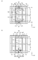
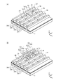
- (A) is a schematic perspective view showing an example of the missing portion 3a occurring in the column bank 14a, and (b) is a pair of repair banks 5X1, 5X2 formed so as to sandwich the missing portion 3a in the Y direction. It is a schematic perspective view which shows a mode.
- FIG. 6 is a schematic process diagram illustrating a manufacturing process of the display panel according to the embodiment. It is a schematic cross section which shows a part of manufacturing process of the display panel which concerns on embodiment. It is a figure which shows typically the method of apply
- FIG. 7A is a schematic plan view showing the application position of the repair material by the needle dispenser, which is set around the missing portion of FIG. 7A, and FIG. 7B shows a state in which a weir is formed.
- FIG. 8A is a schematic plan view showing the application position of the repair material by the needle dispenser, which is set around the missing portion of FIG. 8A, and FIG. 8B shows a state in which a weir is formed. It is a schematic plan view.
- (A)-(g) is a schematic cross-sectional view showing a state in which a dam portion is formed by applying a repair material with a needle dispenser.
- (A) is a schematic cross-sectional view showing the state of the tank and the needle before applying the repair material.
- (B) is a schematic cross-sectional view showing a state in which the repair material attached to the needle is applied to the application point P1.
- (C) is a schematic cross-sectional view showing a state in which the needle is being moved upward.
- (D) is a schematic cross-sectional view showing a state in which the needle is moved upward.
- (E) is a schematic cross-sectional view showing a state in which the needle and the tank are moved to apply the repair material to the application point P2.
- FIG. 11A is a partially enlarged cross-sectional view of the display panel according to the embodiment taken along line BB in FIG. 11B, taken along line CC in FIG. 11B, and taken along line DD in FIG. 11C. Is.
- (A) (b) It is a schematic plan view which shows the state of the display panel in which the dam part assumed as a comparative example was formed. 5 is a schematic plan view showing a state in which an ink layer is formed on the display panel 100.
- FIG. 17A is a schematic plan view showing a state where the weir portion of FIG. 17B is formed
- FIG. 18A is a schematic plan view showing a state where the weir portion of FIG. 18B is formed. ..
- a method of manufacturing a line bank organic EL display panel a plurality of long banks extending in the column direction and formed in parallel are formed on a substrate, and an organic light emitting material is included in a gap between the plurality of banks.
- a light emitting layer is formed by applying ink.
- the line bank method since the ink can flow in the gap along the bank, variations in the film thickness at the time of ink application are made uniform by the flow of the ink, and a light emitting layer having a uniform film thickness is formed. be able to. As a result, it is possible to manufacture an organic EL display panel with less uneven brightness.
- the ink applied in the gap may penetrate into the adjacent gap through the defect, and a mixed color region where inks of different emission colors are mixed may occur.
- display quality may deteriorate over a plurality of pixels.
- a color mixture is displayed by forming a weir at a predetermined distance in the column direction from the defect in a gap on both sides of the defect in the row direction.
- a technique is disclosed in which the occurrence of quality deterioration is limited to the sub-pixels on both sides of the defect in the row direction.
- Patent Document 1 For a defect in which a part of a long bank is missing in the manufacturing process, when the missing part has a predetermined length in the long direction, the method described in Patent Document 1 causes color mixing. It may be difficult to suppress the expansion of the.
- FIG. 17A is a schematic perspective view showing an example of a missing portion that occurs in a bank of a display panel having a long bank.
- the main components of the display panel are the base substrate 11, the pixel electrodes 12 arranged in a matrix in the XY directions, the hole injection layer 13, and the Y direction arranged between the pixel electrodes 12 ( A column bank 14a extending in the column direction and a row bank 24 extending in the X direction (row direction) and having a low height, an organic light emitting layer, an electron transport layer, a common electrode, and a sealing layer are provided. Then, the sub-pixels are arranged in a matrix corresponding to the pixel electrodes 12 of light-emitting elements having an organic light-emitting layer corresponding to any of red (R), green (G), and blue (B) emission colors. There is. Note that FIG. 17A shows a state in which the row bank 14a before the electron transport layer, the common electrode, and the sealing layer are formed in the manufacturing process is not yet fired.
- the display panel has a missing portion 3c in which a part of the column bank 14a is missing from the surface of the base substrate 11 and a part of the elongated column bank 14a does not exist. Both ends 3c1 and 3c2 of the missing portion 3c are located on the pixel electrodes 12c1 and 12c2, respectively, and the missing portion 3c has a positional relationship in which the positions in the Y direction are the same as those of the two pixel electrodes 12c1 and 12c2 at least in part. Therefore, it is difficult to suppress the expansion of color mixture by the method described in Patent Document 1 in which a weir is formed at a position apart from the defective portion in the Y direction by a predetermined distance.
- FIG. 17( b) is a schematic perspective view showing a mode of the display panel in which the weir portion that the inventor recalled is formed for the defective portion 3 c.
- FIG. 19A is a schematic plan view showing a state in which the weir portion of FIG. 17B is formed. Note that FIG. 17B shows a state before the electron transport layer, the common electrode, and the sealing layer are formed in the manufacturing process, and after firing of the column bank 14a.
- the pixel electrodes 12c1 and 12c2 are provided above the pixel electrodes 12c1 and 12c2 in the two gaps 20 between the column banks 14 in which the missing portions 3 are present and the column banks 14 adjacent to each other in the row direction.
- the pair of repair row banks 52X1 and 52X2 are formed at the positions A1 and A2 which are separated from each other by a predetermined distance A1 to A2 in the column direction.
- the positions A1 and A2 may be positions above the pixel electrodes 12c1 and 12c2 and at which the distance in the Y direction is maximum.
- repair row banks 52X1 and 52X2 are respectively formed to form weirs 501 and 502, and the pair of weirs 501 and 502 makes the gap 20 a first space SA that is a space portion close to the missing portion 3. , And is divided into two second spaces SB composed of space portions that are not close to each other. As a result, it is possible to keep the mixed colors in the first space SA and prevent the mixed colors from flowing out to the second space SB.
- FIG. 18(a) is a schematic perspective view showing another example of a missing portion occurring in a bank
- FIG. 18(b) is a schematic perspective view showing a weir portion that the inventor recalled is formed around the missing portion. It is a figure.
- FIG. 19B is a schematic plan view showing a state in which the weir portion of FIG. 18B is formed.
- the missing portion 3d has the same position in the Y direction as the two pixel electrodes 12c1 and 12c2, and a part of the second row bank 24 sandwiching the pixel electrodes 12c1 and 12c2 in the Y direction.
- the positions in the Y direction overlap.
- a pair of repair row banks 52X1 and 52X2 are provided at positions A1 and A2 above the pixel electrodes 12d1 and 12d2 and separated by a predetermined distance A1 to A2 in the column direction.
- the present invention has led to the idea of a method for manufacturing an organic EL display panel and an organic EL display panel according to the present disclosure, after earnestly studying a structure for blocking the light and its manufacturing method.
- An organic EL display panel according to an embodiment of the present disclosure, a substrate, a plurality of pixel electrodes arranged in a matrix on the upper surface of the substrate, between the pixel electrodes adjacent in at least the row direction on the substrate, A plurality of elongated column banks formed in parallel with each other extending in the column direction, a missing portion where a part of the elongated column bank does not exist, and the missing portion above the pixel electrode.
- a common electrode is provided above the light emitting layer, the repair bank is present in the two gaps, and is above the pixel electrode having the same position in the column direction at least partially in the column direction.
- a pair of repair row banks formed at positions separated from each other in the column direction by a predetermined distance or more, an end of the repair row bank not connected to the column bank in the row direction, and a missing portion A repairing column bank that connects the closest portion of the column bank in the column direction is included.
- the range of the sub-pixel in which the display quality is deteriorated due to the lack in the completed organic EL display panel is at least the position of the missing part and the column direction. It can be limited to subpixels including pixel electrodes that are partly the same.
- the pair of repair row banks may be formed at a position where the distance in the column direction is maximum.
- Part includes an organic light-emitting material contained in a light-emitting layer formed in a gap facing each other in the row direction with the cutout portion interposed therebetween, and light emission formed outside the range sandwiched between the pair of repair row banks.
- the layer portion may be configured not to include the organic light emitting material included in the light emitting layer formed in the facing gap.
- the mixed color area is limited to the range of the sub-pixel in which the position in the Y direction and the position in the Y direction are at least partly the same, and the deterioration of the display quality due to the color mixture is suppressed in the sub pixel in which the missing part and the part in the Y direction overlap.
- a plurality of long electrodes extending in the row direction and formed in parallel are provided between the pixel electrodes adjacent to each other in at least the column direction on the substrate. It may be configured such that a row bank having a circular shape is provided, and the closest portion of the column bank having a missing portion is located on the upper surface of the row bank.
- the display quality is improved due to the missing. It is possible to limit the range of sub-pixels that fall.
- a portion of the pixel electrode located below the row bank has a contact hole in which a part of the surface of the pixel electrode is recessed, and the repair is performed.
- the row bank may be formed at a position that does not overlap the contact hole in a plan view.
- the method for manufacturing an organic EL display panel includes a step of preparing a substrate, a step of forming a plurality of pixel electrodes arranged in a matrix on the upper surface of the substrate, and There is a step of forming a plurality of elongated column banks formed in parallel with each other and extending in the column direction between at least the pixel electrodes adjacent to each other in the row direction, and a part of the elongated column banks is present. And a pair of repair banks in each of the two gaps between the column banks adjacent to both sides in the row direction of the column bank in which the missing portion is detected above the pixel electrode.
- the repair bank exists above the pixel electrode that is present in the two gaps and has the same position in the column direction at least in part in the column direction, and a predetermined distance or more in the column direction.
- the range of sub-pixels in which the display quality is deteriorated due to the missing is the pixel electrode whose position in the column direction is at least partly the same as the missing part. It is possible to manufacture an organic EL display panel that can be limited to subpixels including
- the pair of repair row banks may be formed at a position where the distance in the column direction is maximum.
- the repair row bank is formed above the pixel electrode, so that the repair row bank formed on the upper surface of the flattening layer has a height corresponding to the thickness of the pixel electrode. It is possible to suppress the disadvantage that the height is insufficient, and the disadvantage that the material of the repair row bank wets the flattening layer or the row bank and flows before hardening and hardening.
- the ink applied to any of the two gaps is sandwiched between the pair of repair row banks.
- the ink applied to the above range flows out through the missing section into the gap facing the row direction across the missing section, and is blocked in the range in the column direction by the pair of repair row banks.
- the mixed color area is limited to the range of the sub-pixel in which the position in the Y direction is the same as the position in the Y direction at least in part, and the deterioration of the display quality due to the color mixture is suppressed in the Y direction.
- a display panel limited to the inside can be manufactured.
- a plurality of elongated shapes that are formed in parallel with each other and extend in the row direction between at least the pixel electrodes adjacent to each other in the column direction on the substrate.
- the step of forming the row bank may be configured such that the closest portion of the column bank having the missing portion is located on the upper surface of the row bank.
- any one of the above aspects there is a step of forming a contact hole in which a part of the surface of the pixel electrode is recessed, in a portion of the pixel electrode located below the row bank.
- the repair column bank may be formed at a position not overlapping the contact hole in plan view.
- FIG. 1 is a schematic block diagram showing the configuration of an organic EL display device 1 having a display panel 100 according to the embodiment.
- the organic EL display device 1 has a display panel 100 and a drive control unit 101 connected thereto.
- the display panel 100 is a panel that utilizes the electroluminescence phenomenon of an organic material, and as shown in FIG. 2, a plurality of light emitting elements (organic EL elements) 10 are arranged in a matrix on a substrate.
- the drive control unit 101 is composed of four drive circuits 102 to 105 and a control circuit 106.
- the arrangement of the drive control unit 101 with respect to the display panel 100 is not limited to this.
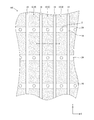
- FIG. 2 is a plan view schematically showing a schematic configuration as viewed from the display surface side of the display panel 100.
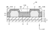
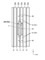
- FIG. 3 is a partially enlarged sectional view of the display panel 100 taken along the line AA of FIG.
- the display panel 100 is a so-called top emission type and has a display surface on the Z direction side.
- the configuration of the display panel 100 will be described with reference to FIGS.
- the display panel 100 mainly includes a base substrate 11, a pixel electrode 12, a hole injection layer 13, a column bank 14, an organic light emitting layer 15, an electron transport layer 16, a common electrode 17, and a seal.
- a stop layer 18 is provided.
- the hole injection layer 13 and the electron transport layer 16 correspond to the functional layer, and the pixel electrode 12 and the common electrode 17 sandwich the functional layer.
- the light emitting elements 10R, 10G, and 10B having the organic light emitting layer 15 corresponding to any of the red (R), green (G), and blue (B) emission colors are subpixels, and as shown in FIG. Subpixels are arranged in a matrix.
- FIG. 2 shows a state in which the electron transport layer 16, the common electrode 17, and the sealing layer 18 are removed.
- the base substrate 11 has a substrate body 11a, a TFT (thin film transistor) layer 11b, and a flattening layer 11c.
- the substrate main body 11a is a portion that serves as a base material of the display panel 100, and can be formed of an insulating material such as non-alkali glass, soda glass, polycarbonate resin, polyester resin, or alumina. Further, the substrate body 11a may be formed using a polyimide material.
- the TFT layer 11b is provided on the surface of the substrate body 11a for each sub-pixel, and a pixel circuit including a thin film transistor element is formed on each of the sub-pixels.
- the flattening layer 11c is formed on the TFT layer 11b.
- the flattening layer 11c is made of an organic insulating material such as a polyimide resin, an acrylic resin, a novolac type phenol resin, or an inorganic insulating material such as SiO (silicon oxide) or SiN (silicon nitride). It has a function of ensuring electrical insulation between and, and flattening even if there is a step on the upper surface of the TFT layer 11b to suppress the influence on the underlying surface on which the pixel electrode 12 is formed.
- the pixel electrode 12 is a pixel electrode individually provided on the base substrate 11 for each sub-pixel, and is, for example, Ag (silver), Al (aluminum), aluminum alloy, Mo (molybdenum), APC (silver, palladium). , A copper alloy) or the like. In this embodiment, the pixel electrode 12 is an anode.
- a known transparent conductive film may be further provided on the surface of the pixel electrode 12.
- a material of the transparent conductive film for example, indium tin oxide (ITO) or indium zinc oxide (IZO) can be used.
- ITO indium tin oxide
- IZO indium zinc oxide
- the transparent conductive film is interposed between the pixel electrode 12 and the hole injection layer 13 and has a function of improving the bondability between the layers.
- the hole injection layer 13 is, for example, an oxide of silver (Ag), molybdenum (Mo), chromium (Cr), vanadium (V), tungsten (W), nickel (Ni), iridium (Ir), or PEDOT.
- a layer made of a conductive polymer material such as (a mixture of polythiophene and polystyrene sulfonic acid).
- the hole injection layer 13 made of a metal oxide has a function of injecting and transporting holes to the organic light emitting layer 15 in a stable manner or assisting the generation of holes.
- the row bank 14 is made of an insulating organic material (for example, acrylic resin, polyimide resin, novolac type phenol resin, etc.).
- each column bank 14 is trapezoidal as shown in FIG. 3, and a gap 20 (20R, 20G, 20B) partitioned by the column banks 14 is formed between the column banks 14, and A plurality of pixel electrodes 12 are arranged in a row in the Y direction at the bottom of the gap 20, and a hole injection layer 13, an organic light emitting layer 15, and an electron transport layer 16 as functional layers are formed thereon.
- the row bank 14 partitions the light emitting elements 10 adjacent to each other in the X direction and also functions as a structure that prevents the applied ink from overflowing when the organic light emitting layer 15 is formed by the wet method.
- the row bank 24 has a height lower than that of the column bank 14 (see FIG. 7 ), is formed between the pixel electrodes 12 adjacent to each other in the Y direction in each gap 20, and the light emitting elements adjacent to each other in the Y direction. 10 sections are divided. That is, the display panel 100 is an organic EL display panel having a so-called line bank.
- Each row bank 24 has a strip shape that extends in the X direction (row direction), passes under the column bank 14 and is connected to the adjacent row bank 24 and extends in the X direction. Therefore, the entire column banks 14 and row banks 24 are formed in a grid pattern on the base substrate 11 (see FIG. 2).
- the missing portion 3 refers to a portion in which a part of the column bank 14a is missing from the surface of the flattening layer 11c and a part of the elongated column bank 14a does not exist. Such a dropout of the column bank 14a occurs accidentally in manufacturing the column bank 14a. For example, in the step of exposing the bank material layer, a portion where the exposure is insufficient and the polymerization is not sufficiently generated occurs by being washed away in the next developing step. When the missing portion 3 is generated in this way, color mixing occurs between the ink layers 15a formed in the gaps adjacent to each other through the missing portion 3. Therefore, in the portion where the missing portion 3 is generated in the column bank 14a, color mixture of inks having different emission colors occurs, which causes defective emission color. Therefore, this portion is a defect.
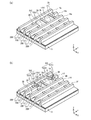
- FIG. 4A is a schematic perspective view showing an example of the missing portion 3a occurring in the column bank 14a.
- one end 3 a 1 of the missing portion 3 a in the Y direction is located between the row banks 24 adjacent to each other in the Y direction, and the other end 3 a 2 of the missing portion 3 a is located on the row bank 24.
- FIG. 5A is a schematic perspective view showing an example of a missing portion 3b longer than the missing portion 3a occurring in the column bank 14a.
- one end 3b1 of the missing portion 3b in the Y direction is located between the row banks 24, and the other end 3b2 of the missing portion 3b is also located on another row bank 24.
- the missing portion 3 is used.
- the defect occurring in the column bank 14a is not limited to the above-mentioned missing portion 3. If a foreign substance enters one column bank 14a and the foreign substance penetrates the wall surface of the column bank 14 to the adjacent gap 20, it is also a defect. For example, when foreign matter adheres to the row bank 14a and is defective, even if there is foreign matter inside or below the row bank 14a, if the adhesion between the foreign matter and the bank material is poor, a gap is created. This creates a flow path for the ink, resulting in a defect. Therefore, this causes color mixing between the ink layers 15a formed in the adjacent gaps with the foreign matter in between.
- the present disclosure is intended to repair the missing portion 3 among various defects.
- repair bank 52 The configuration of the repair bank 52 will be described below.
- FIG. 4B is a schematic perspective view showing a state in which a pair of repair banks 5X1 and 5X2 are formed so as to sandwich the missing portion 3a in the Y direction.
- FIG. 4B it is above the pixel electrodes 12a1 and 12a2 (the pixel electrodes 12a if not distinguished) whose positions in the Y direction are at least partially the same in the Y direction as in the column direction.
- a pair of repair row banks 52X1 and 52X2 (which are referred to as repair row banks 52X if not distinguished) are formed at positions A1 and A2 that are separated by a predetermined distance A1 to A2 or more.
- the positions A1 and A2 may be positions above the pixel electrodes 12a1 and 12a2 and at which the distance in the Y direction becomes maximum.
- repair row bank 52X is formed on the row bank 24, for example, both are made of an organic material, so that the affinity is high and the material of the repair row bank 52X is wet on the row bank 24. It may spread easily and may not be formed up to a sufficient height as a weir for the repair row bank 52X.
- FIG. 4B by forming the repair row bank 52X above the pixel electrode 12A, the required height of the repair row bank 52X can be secured.
- the two gaps 20 are formed above the pixel electrodes 12a1 in the two gaps 20 between the column banks 14 having the missing portions 3a and the column banks 14 on both sides in the X direction.
- the repair row bank 52X1 has a structure in which the ends on both sides in the X direction are connected to the column banks 14 that are adjacent to each other in the X direction, and a weir 501 that connects the column banks 14 can be constructed.
- the repair row bank 52X2 formed in the pixel electrode 12a2 has a structure in which the end on the side of the missing portion 3a in the X direction is not connected to the adjacent column bank 14 in the X direction, and a weir that connects the column banks 14 is formed. Can not be built. Therefore, a configuration is added in which a repair column bank 52Y2 that connects the end of the repair row bank 52X2 that is not connected to the column bank 14 in the X direction and the column bank 14 that is closest to the end in the Y direction is added. take. That is, the repair bank 52 formed on the pixel electrode 12a2 has an L-shaped configuration in a plan view, which includes the repair row bank 52X2 and the repair column bank 52Y2.
- the repair banks 52 formed above the pixel electrodes 12a2 in the two gaps 20 between the column banks 14 having the missing portions 3a and the column banks 14 on both sides in the X direction respectively have end portions on both sides. Are connected to the column banks 14 adjacent to each other in the X direction.
- the repair bank 52 including the repair row bank 52X1 is formed in each of the gaps 20 on both sides of the column bank 14 having the missing portion 3a to form the weir 501.
- the weir 502 is formed by forming the repair bank 52 including the repair row bank 52X2 and the repair column bank 52Y2.
- the gap 20 is partitioned by the pair of weirs 501 and 502 into a first space SA including a space portion close to the missing portion 3 and two second spaces SB including a space portion not close to the missing portion 3. ing.
- FIG. 5B is a schematic perspective view showing a state in which a pair of repair banks 5X1 and 5Y1, 5X2 and 5Y2 are formed so as to sandwich the missing portion 3b in the Y direction.
- FIG. 5(b) it is above the pixel electrodes 12b1 and 12b2 (the pixel electrodes 12b if not distinguished) whose positions in the Y direction are at least partially the same in the Y direction as in the column direction.
- a pair of repair row banks 52X1 and 52X2 (which are referred to as repair row banks 52X if not distinguished) are formed at positions A1 and A2 that are separated by a predetermined distance A1 to A2 or more.
- the positions A1 and A2 may be positions above the pixel electrodes 12b1 and 12b2 and having a maximum distance in the Y direction.
- the repair row banks 52X1 and 52X2 formed on the pixel electrodes 12b1 and b2 are arranged such that the end portions on the side of the missing portion 3b in the X direction are adjacent to the adjacent column banks 14 and X. Since the structure is not connected in the direction, a weir that connects the row banks 14 cannot be constructed. Therefore, repair column banks 52Y1 and 52Y2 that connect in the Y direction the ends of the repair row banks 52X1 and 52X2 that are not connected to the column bank 14 in the X direction and the column banks 14 that are closest to the ends are provided. The added configuration is adopted.
- the repair bank 52 formed on the pixel electrode 12b1 includes a repair row bank 52X1 and a repair column bank 52Y1
- the repair bank 52 formed on the pixel electrode 12b2 includes a repair row bank 52X2 and a repair row bank 52X2.
- the row bank 52Y2 has an L-shaped configuration in plan view.
- the repair bank 52 including the repair row bank 52X1 and the repair column bank 52Y1 is provided in each of the gaps 20 on both sides in the X direction of the column bank 14 having the missing portion 3b.
- the weir 501 is formed by forming the weir 501, and the repair bank 52 including the repair row bank 52X2 and the repair column bank 52Y2 is formed to form the dam 502.
- the gap 20 is partitioned by the pair of weirs 501 and 502 into a first space SA including a space portion close to the missing portion 3 and two second spaces SB including a space portion not close to the missing portion 3. ing.
- the width of the repair bank 52 is, for example, 5 to 50 ⁇ m.
- the pair of weirs 501 and 502 dam the mixed color ink to prevent the mixed color region from expanding.
- the organic light emitting layer 15 is a site where carriers (holes and electrons) are recombined to emit light, and contains an organic material corresponding to any one of R, G, and B colors.
- the organic light emitting layer 15 is formed in the groove-shaped gaps (see the gaps 20R, 20G, and 20B in FIG. 7) that are divided by the column banks 14 and extend in the Y direction.
- the gap 20R shown in FIG. 7 is a gap in which the red light emitting layer is formed to form the red light emitting element 10R, and the gap 20G and the gap 20B are formed in green and blue light emitting layers, respectively. , A gap where the blue light emitting elements 10G and 10B are formed.
- the organic light emitting layers 15 having different colors are arranged so as to sandwich the column bank 14.
- Examples of the material of the organic light emitting layer 15 include polyparaphenylene vinylene (PPV), polyfluorene, oxinoid compounds, perylene compounds, coumarin compounds, azacoumarin compounds, oxazole compounds, oxadiazole compounds, perinone compounds, pyrrolopyrrole compounds, naphthalene.
- PV polyparaphenylene vinylene
- polyfluorene polyfluorene
- oxinoid compounds perylene compounds
- coumarin compounds coumarin compounds
- azacoumarin compounds oxazole compounds
- oxadiazole compounds oxadiazole compounds
- perinone compounds pyrrolopyrrole compounds
- naphthalene naphthalene.
- a pair of repair banks 52 are formed in the gaps 20 on both sides of the column bank 14 having the missing portion 3, and both ends of the repair bank 52 are connected to the column banks 14 on both sides in the X direction. They are connected to form weirs 501 and 502. Therefore, the gap 20 is partitioned by the pair of weirs 501 and 502 facing each other in the Y direction into the first space SA that is close to the missing portion 3 and the two second spaces SB that are not close to each other, and the color is mixed in the first space SA. Even if there is a region, the mixed color region does not extend beyond the repair bank 52 to the second space SB.
- the organic light emitting layer 15 formed in one of the two gaps 20 facing each other in the row direction with the cutout portion 3 interposed therebetween was formed in the range sandwiched by the pair of repair row banks 52X1 and 52X2.
- the portion of the organic light emitting layer 15 includes the organic light emitting material contained in the organic light emitting layer 15 formed in the gap 20 opposed to each other in the row direction with the missing portion 3 interposed therebetween, and is sandwiched between the pair of repair row banks 52X1 and 52X2.
- the portion of the organic light emitting layer 15 formed outside the defined range can realize a structure that does not include the organic light emitting material contained in the organic light emitting layer 15 formed in the facing gap 20.
- the electron transport layer 16 has a function of transporting electrons injected from the common electrode 17 to the organic light emitting layer 15, and includes, for example, an oxadiazole derivative (OXD), a triazole derivative (TAZ), a phenanthroline derivative (BCP, Bphen) and the like.
- OXD oxadiazole derivative
- TEZ triazole derivative
- BCP phenanthroline derivative
- the common electrode 17 is formed of, for example, a light-transmitting material having conductivity such as ITO or IZO, and is provided over all the sub-pixels.
- the common electrode 17 is a cathode.
- the sealing layer 18 is provided to protect the hole injection layer 13, the organic light emitting layer 15, the electron transport layer 16, and the common electrode 17 from moisture and oxygen.
- a black matrix, a color filter, etc. may be formed on the sealing layer 18.
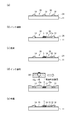
- FIG. 6 is a schematic process diagram showing a manufacturing process of the display panel 100.
- FIG. 7 is a sectional view schematically showing a part of the manufacturing process of the display panel 100.
- a method of manufacturing the display panel 100 will be described based on the process chart of FIG. 6 with reference to FIGS.
- the TFT layer 11b is formed on the substrate body 11a (step S1).
- a flattening layer 11c is formed on the TFT layer 11b by a photoresist method using an organic material having excellent insulating properties to manufacture the base substrate 11 (step S2).
- the flattening layer 11c has a thickness of, for example, about 4 ⁇ m.
- the contact hole 2 is formed when the planarizing layer 11c is formed.
- a pixel electrode made of a metal material and having a thickness of about 200 [nm] is formed on the base substrate 11 by a vacuum deposition method or a sputtering method (step S3).
- a hole injection layer made of tungsten oxide is uniformly formed on the base substrate 11 and the pixel electrode by a sputtering method or the like (step S4).
- the pixel electrode 12 and the hole injection layer 13 are formed by patterning for each sub-pixel by the photolithography method (step S5).
- the row bank 24 and the column bank 14 are formed by the photolithography method as follows.
- a bank material for example, a photoresist material having photosensitivity
- a bank material for example, a photoresist material having photosensitivity
- a photomask having openings matching the pattern of the row bank 24 is overlaid on the applied bank material layer, and UV irradiation is performed for exposure. Then, the unburned row bank 24a is formed by removing the uncured excess bank material with a developing solution. Then, the row bank 24 that has not been fired is heated and fired to form the row bank 24 (step S7).
- a bank material for example, a negative photosensitive resin composition for forming the column banks 14 is uniformly applied on the substrate on which the row banks 24 are formed.
- a mask having an opening matching the pattern of the column bank 14 to be formed is overlaid on the bank material layer, and exposure is performed from above the mask. Then, the excess bank material is washed out with an alkali developing solution to pattern the bank material to form a row bank pattern (step S6). Then, the unbaked column bank 14 is heated and baked to form the row bank 14 (step S7). This firing is performed, for example, by heating the unfired row bank 14 at a temperature of 200° C. to 240° C. for 60 minutes.
- a row bank 24 and a column bank 14 are patterned as shown in FIG.
- a gap 20 is formed between the adjacent column banks 14.
- step S8 the occurrence of a missing portion in this pattern-formed column bank 14 is checked (step S8), and if there is a missing portion, it is repaired.
- FIG. 7B shows a state in which the repair material is applied to the gaps 20 between the row banks 14 (step S9) and the unbaked repair banks 52a are formed.
- step S10 After that, by heating and firing the unbaked repair bank 52a, the repair bank 52 is completed in addition to the column bank 14 and the row bank 24, and the repair of the missing portion 3 is completed (step S10).
- This firing is performed, for example, by heating the unfired repair bank 52a at a temperature of 200° C. to 240° C. for 60 minutes.
- FIG. 7C shows a state in which the row bank 14 is formed and the repair bank 52 is formed by this firing, that is, the missing portion 3 in the row bank 14 is repaired.
- the column bank 14 thus formed may be further subjected to a process of adjusting the contact angle of the column bank 14 with respect to the ink applied in the next step.
- a process of adjusting the contact angle of the column bank 14 with respect to the ink applied in the next step may be performed.
- surface treatment with a predetermined alkaline solution, water, organic solvent, or the like, plasma treatment, or the like may be performed.
- a material having liquid repellency may be used as the bank material of the column bank.
- the row bank and the weir are fired separately here, but they may be fired simultaneously. That is, here, the processing is performed in the order of forming the row bank, firing the row bank, detecting the missing portion, forming the weir portion, and firing the weir portion, but forming the row bank, detecting the missing portion, and the weir.
- the processing may be performed in the order of formation of the parts, firing of the row banks and firing of the dam.
- ink for forming the organic light emitting layer 15 is applied to the gap 20 between the adjacent row banks 14.
- This ink is a mixture of an organic material forming the organic light emitting layer 15 and a solvent, and is applied in each gap 20 by an inkjet method. The method of applying the ink in the gap 20 by the inkjet method will be described in detail later.
- Step S11 the solvent contained in the applied ink layer 15a is evaporated and dried, and if necessary, heated and baked to form the organic light emitting layer 15 in each gap 20, as shown in FIG. 7(e).
- a material forming the electron transport layer 16 is formed on the organic light emitting layer 15 and the column bank 14 by a vacuum vapor deposition method to form the electron transport layer 16 (step S12).
- a material such as ITO or IZO is formed by a sputtering method or the like to form the common electrode 17 (step S13).
- a light-transmissive material such as SiN or SiON is formed on the surface of the common electrode 17 by a sputtering method, a CVD method or the like to form the sealing layer 18 (step S14).
- the display panel 100 is completed through the above steps.
- the ink 15a which is a solution for forming the organic light emitting layer 15 is used to form the organic light emitting layer 15R in the gap 20R for the red subpixels and the organic ink in the gap 20G for the green subpixels.
- the organic light emitting layer 15B is formed in the light emitting layer 15G and the gap 20B for the blue sub-pixel in each region between the plurality of line banks.
- the organic light emitting layer 15R and the organic light emitting layer 15G or the organic light emitting layer 15B may have different thicknesses.
- the thickness of the organic light emitting layer 15R becomes smaller than that of the organic light emitting layer 15B and the organic light emitting layer 15G. It can be formed larger than the thickness.
- the amount of ink ejected from the nozzle is set to the first condition, the ink is applied to the plurality of first color gaps 20 on the substrate, and then the ink is ejected from the nozzle.
- the amount of ink is set to the second condition, the ink is applied to the plurality of second color gaps 20 on the substrate, and then the amount of ink ejected from the nozzle is set to the third condition and the substrate is set.
- Ink is sequentially applied to the gaps of all three colors by the method of applying ink to the plurality of gaps 20 of the third color.
- the ink is applied to the gap 20 of the second color of the substrate, and the ink is further applied to the gap 20 of the third color of the substrate.
- the step of applying is repeatedly performed, and the inks for the three color gaps 20 are sequentially applied.
- the nozzles for ejecting ink different nozzles may be used, one for ejecting the first color ink, one for ejecting the second color ink, and one for ejecting the third color ink. Good.
- FIG. 8 is a diagram showing a process of applying the light emitting layer forming ink to the substrate, and is a schematic diagram in the case of uniformly applying to the gaps 20 between the row banks 14.
- the organic light emitting layer 15 continuously extends not only to the light emitting region (the region surrounded by the column bank 14 and the row bank 24 in FIG. 2) but also to the adjacent non-self light emitting region (the region on the row bank 24 in FIG. 2). It has been stretched. With this configuration, when the organic light emitting layer 15 is formed, the ink applied to the light emitting region can flow in the column direction through the ink applied to the non-self light emitting region, and the film thickness is leveled among the pixels in the column direction. can do. Therefore, large unevenness in film thickness is less likely to occur in the column direction, and unevenness in brightness and shortening of life of each pixel are improved.
- the substrate is placed on the work table of the droplet discharge device with the column bank 14 along the Y direction, and the plurality of discharge ports 3031 are arranged in a line along the Y direction. While scanning the head 301 in the X direction, the ink is landed from each ejection port 3031 toward the landing target set in the gap 20 between the row banks 14.
- the area where the ink is applied to the organic light emitting layer 15 with the same application amount is one of the three areas that are arranged adjacent to each other in the x direction.
- the method for forming the organic light emitting layer 15 is not limited to this, and the ink is dropped by a method other than the inkjet method or the gravure printing method, for example, a known method such as a dispenser method, a nozzle coating method, a spin coating method, an intaglio printing, or a letterpress printing. ⁇ Can be applied.
- the missing portion 3 in the row bank 14a is detected by, for example, capturing a surface image of the row bank 14a formed on the base substrate 11 and inspecting the surface image for a pattern.
- FIG. 9 is a schematic configuration diagram showing an example of a repair device used for detecting a bank missing portion and repairing it.
- a base 202 is provided with a table 202 on which the above-mentioned base substrate 11 is placed, and an imaging device 211 and a head portion 210 to which a needle dispenser 213 is attached. Then, the table 202 can be moved in the Y direction based on the instruction of the CPU 231 of the controller 230, and the head unit 210 can be moved in the X direction and the Z direction according to the instruction of the CPU 231.
- the needle dispenser 213 attached to the head unit 210 is in the X direction, the Y direction, and the Z direction with respect to the base substrate 11 above the base substrate 11 placed on the table 202 according to the instruction of the CPU 231. Can move relative to.
- a substrate 11 on which the pixel electrodes 12, the hole injection layers 13, the column banks 14 a, and the row banks 24 are formed is shown as the underlying substrate 11.
- the repair bank 52 is formed by applying the repair material from the needle dispenser 213 to a plurality of positions set along the line (the repair bank forming line) in which the repair bank 52 is to be formed in the gap 20. By doing.
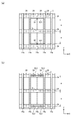
- FIG. 10A is a schematic plan view showing the application position of the repair material by the needle dispenser, which is set around the missing portion 3a of FIG. 4A.
- the 10A represent application positions by the needle dispenser set along the lines LX1 and LX2.
- the lines LX1 and LX2 may be set above the pixel electrodes 12a1 and 12a2 at positions where the distances between the lines LX1 and LX2 in the Y direction are maximum.
- one end 3a1 of the missing portion 3a in the Y direction is located between the row banks 24 adjacent to each other in the Y direction. Therefore, in the pixel electrode 12a1, the position of the line LX1 in the Y direction is located above the coordinate of the end 3a1 of the missing portion 3a in the Y direction. Therefore, it is determined that the end portion of the repair bank 52X1 formed on the line LX1 is connected to the column bank 14a.
- the other end 3a2 of the missing portion 3a is located on the row bank 24. Therefore, in the pixel electrode 12a2, the position of the line LX2 in the Y direction is located above the coordinates of the end 3a2 of the missing portion 3a in the Y direction. Therefore, it is determined that the end portion of the repair bank 52X2 formed on the line LX2 is not connected to the column bank 14a.
- a repairing column bank forming line LY2 (hereinafter referred to as line LY2) is set in the Y direction from P4 closest to the missing portion 3a among the points P1 to P4 to at least the end 3a2 in the Y direction of the missing portion 3a.
- Points P5 to P7 shown in FIG. 10A represent application positions by the needle dispenser set along the line LY2. At this time, the point P7 needs to be set at a position on the row bank 24 in a plan view.
- FIG. 11A is a schematic plan view showing the application position of the repair material by the needle dispenser, which is set around the missing portion 3b.
- pixel electrodes 12b1 and 12b2 whose positions in the Y direction are at least partially the same in the Y direction based on the coordinate positions of both ends 3b1 and 3b2 in the Y direction of the lacking unit 3b. Identify. Then, the lines LX1 and LX2 in the X direction are set at the positions A1 and A2 above the pixel electrodes 12b1 and 12b2. The application points P1 to P4 by the needle dispenser are set along the lines LX1 and LX2.
- both ends 3b1 and 3b2 of the missing portion 3b in the Y direction are located on the upper surfaces of the row banks 24 that are adjacent to each other in the Y direction. for that reason.
- the position of the line LX1 in the Y direction is located below the coordinates of the end 3b1 of the missing portion 3b in the Y direction, and the position of the line LX2 in the Y direction is located above the coordinates of the end 3b2 of the missing portion 3b in the Y direction.
- lines LY1 and LY2 are set in the Y direction from P4 closest to the missing portion 3a among points P1 to P4 to at least both ends 3b1 and 3b2 in the Y direction of the missing portion 3a.
- Points P5 to P7 shown in FIG. 10A represent application positions by the needle dispenser set along the lines LY1 and LY2. At this time, the point P7 needs to be set at a position on the row bank 24 in a plan view.
- (Applying and firing repair material) 12A to 12G are diagrams schematically showing how the repair bank 52 is formed by sequentially applying the repair material to the application points P1, P2,....
- the repair device 200 is for repairing by sequentially applying the repair material with the needle 213a at the application points P1, P2, P3, P4 or P1, P2, P3, P4, P5, P6, P7 set in this way.
- the bank 52 is formed.
- the needle dispenser 213 has a tank 213b for accommodating the repair material attached to its tip, and the needle 213a moves up and down so as to penetrate the tank 213b, whereby the repair material attached to the needle 213a is measured in microliter units. It is ready to be applied.
- the needle 213a and the tank 213b are positioned above the application point P1 and the needle 213a is moved downward to attach the repair material to the needle 213a.
- the repair material is applied to the application point P1 by bringing 213a close to the application point P1.
- the repair material has fluidity until it is applied, but the peak shape is maintained after the application, and a peak of the repair material is formed at the application point P1 as shown in FIG. 12(c).
- the needle 213a is pulled up into the tank 213b, and the needle 213a and the tank 213b are moved to the application point P2. Then, as shown in FIG. 12E, the needle 213a is moved downward and the needle 213a having the repair material attached thereto is brought close to the application point P2 to apply the repair material to the application point P2.
- the peak of the repair material formed at the application point P2 is connected to the peak of the repair material formed at the application point P1.
- the needle 213a is pulled up and moved to the application point P3.
- a mountain of repair material is formed at application points P3, P4 or P3, P4, P5, P6, P7, and connected to the mountain of repair material at application point P2.
- the repair material piles are continuous in a shape extending from the point A1 on the row bank 14a having the missing portion 3 to the adjacent row bank 14a. Then, the pile of the applied repair material is dried, and if necessary, is exposed to form the repair bank 52.
- the applied repair material is cured, so that the repair bank 52 having more stable physical properties is formed.
- FIG. 10B is a schematic plan view showing a state in which the repair bank 52 is formed around the missing portion 3a of FIG. 4A.
- the lines LX1 and LX2 shown in FIG. 10A are respectively formed in the two gaps 20 between the column bank 14 having the missing portion 3a and the column banks 14 on both sides in the X direction.
- the replenisher is applied with the needle dispenser 213 at the positions of points P1 to P4, points P1 to P4, and points P5 to P7, respectively, and firing using, for example, a laser is performed.
- the repair banks 52 including the repair row banks 52X1 are formed in the gaps 20 on both sides in the X direction of the column bank 14 having the missing portion 3a. End portions of the weir 501 are connected to the column banks 14 adjacent in the X direction. Further, the repair banks 52 each including the repair row bank 52X2 and the repair column bank 52Y2 are formed, and the weir 502 is formed in which both ends are connected to the column banks 14 adjacent in the X direction.
- the gap 20 is formed by the pair of weirs 501 and 502 facing each other in the Y direction, and the gap 20 is composed of the first space SA that is a space portion that is close to the missing portion 3 and the second space SB that is a space portion that is not close to the missing portion 3. It is divided into
- FIG. 11B is a schematic plan view showing a state in which a repair bank 52 is formed around the missing portion 3b of FIG. 5A.
- the lines LX1 and LX2 shown in FIG. 11A are respectively provided in the two gaps 20 between the column bank 14 having the missing portion 3b and the column banks 14 on both sides in the X direction.
- the replenisher is applied by the needle dispenser 213 at the positions of points P1 to P4, points P1 to P4, points P5 to P7, and points P5 to P7, respectively, and firing is performed using, for example, a laser. ..
- the repair banks 52 including the repair row bank 52X1 and the repair column bank 52Y1 are formed in the gaps 20 on both sides of the column bank 14 having the missing portion 3b.
- a weir 501 is formed whose both ends are connected to the column banks 14 adjacent in the X direction.
- the repair banks 52 each including the repair row bank 52X2 and the repair column bank 52Y2 are formed, and the weir 502 is formed in which both ends are connected to the column banks 14 adjacent in the X direction.
- the gap 20 is formed by the pair of weirs 501 and 502 facing each other in the Y direction, and the gap 20 is composed of the first space SA that is a space portion that is close to the missing portion 3 and the second space SB that is a space portion that is not close to the missing portion 3. It is divided into
- the light emitting layer forming step of the next step S9 is performed to limit the color mixture area of ink and to be described later.
- Ink is applied to the first space SA and the second space SB to form the organic light emitting layer 15.
- repair material a resin composition that cures when light or heat is applied can be used.
- the resin examples include curable resins having an ethylenic double bond such as a (meth)acroyl group, an allyl group, a vinyl group, and a vinyloxy group.
- crosslinking agent that crosslinks the resin, for example, an epoxy compound or a polyisocyanate compound may be added.
- a fluorinated polymer having fluorine introduced into the resin structure may be used.
- fluorine By introducing fluorine into the resin of the repair material, it is possible to impart liquid repellency to the repair bank 52 formed.
- various liquid-repellent agents may be added to the resin.
- the addition amount of the liquid repellent is 0.01 to 10 wt %. By setting the addition amount of the liquid repellent in this range, the storage stability of the resin composition is good, and the liquid repellency of the repair bank 52 formed is also good.
- the repair material may be the same as the bank material forming the row bank 14a.
- a solvent and a photopolymerization initiator may be appropriately added to the resin composition constituting the above repair material.
- the solvent has a solubility in the resin, and a solvent with a boiling point of 150-250°C is You may use more than one kind.
- photopolymerization initiator various commercially available photopolymerization initiators can be used.
- the solid content of the repair material is adjusted to, for example, 20 to 90 wt% and the viscosity is adjusted to, for example, 10 to 50 cP (centipoise).
- the addition amount of the photopolymerization initiator is adjusted according to the exposure amount at the time of baking, but is, for example, 0.1 to 50% by weight, preferably 5 to 30% by weight based on the total solid content.
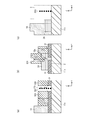
- FIG. 13A is a part of the display panel 100 according to the embodiment taken along line BB in FIG. 11B, taken along line CC in FIG. 11B, and taken along line DD in FIG. 13C. It is an expanded sectional view.
- the flattening layer 11c has a thickness of about 4 ⁇ m
- the column bank 14 has a height of about 1 ⁇ m
- the pixel electrode 12 has a thickness of about 0.2 ⁇ m.
- the height 521 of the weir necessary for preventing the outflow of the ink 15a is approximately 0.7 to 0.8 ⁇ m, and as shown in FIG.
- the repair row bank 52X having a height of 521 or more above the hole injection layer 13).
- the repair row bank is formed by a height corresponding to the thickness of the pixel electrode 12. There is a case where the height of 52X is insufficient and the ink 15a flows out.
- the both have a high affinity because both are made of an organic material, In some cases, the material of the bank (52) easily wets and spreads in the planarization layer 11c and flows, for example, before being cured by a laser, and the repair bank (52) cannot be formed as a weir to a sufficient height.
- the display panel 100 by forming the repair row bank 52X above the pixel electrode 12A, it is possible to secure the required height of the repair row bank 52X.
- the height of the row bank 24 is about 0.5 ⁇ m.
- a concave portion having a depth corresponding to a maximum thickness of about 0.2 ⁇ m of the pixel electrodes is formed.
- a recess having an equivalent depth is formed on the upper surface of the repair column bank 52Y and at the same position.
- the portion of the repair column bank 52Y formed on the upper surface of the row bank 24 is raised by about 0.5 ⁇ m in thickness of the row bank 24. .. Therefore, even if a recess having a maximum depth corresponding to a pixel electrode thickness of about 0.2 ⁇ m exists on the upper surface of the repair column bank 52Y, the height 524 (about 0.7 to 0.8 ⁇ m) required for the weir is increased. ).
- the depth of the contact hole 2 formed in the flattening layer 11c is about 4 ⁇ m, which is the same as the thickness of the flattening layer 11c. Therefore, when the repair column bank 52Y is formed on the upper surface of the repair column bank 52Y above the contact hole 2, a recess having a depth corresponding to about 4 ⁇ m of the flattening layer 11c is formed on the upper surface of the repair column bank 52Y. Since it is formed, the formed repair row bank 52Y cannot secure the height 524 required as a weir. Therefore, it is necessary to form the repair column bank 52Y while avoiding the area above the contact hole 2. In the display panel 100, since the repair column bank 52Y is formed so as to avoid the area above the contact hole 2, the repair column bank 52Y can secure a height necessary for the weir, and can suppress the outflow of ink.
- FIG. 13C is a schematic diagram when it is assumed that the repairing column bank (52) is formed at the same position as the missing portion 3 so as to make up for the missing portion of the column bank 14. ..
- the repairing column bank (52) is formed on the upper surface of the flattening layer 11c between the pixel electrodes 12, the same as in the example shown in FIGS. 13(a) and 13(b). For this reason, the height 524 (about 0.7 to 0.8 ⁇ m) required for the weir cannot be secured.
- 14(a) and 14(b) are schematic plan views showing a state of a display panel on which a weir is supposed as a comparative example.
- FIG. 14A if two gaps 20 are provided between the column banks 14 adjacent to each other on both sides in the row direction of the column bank 14 in which the missing portions 3 are present, they are separated by a predetermined distance A1 to A2 in the column direction.
- FIG. 7 is a schematic plan view when it is assumed that a pair of repair row banks 52I that cross two gaps 20 are formed at the positions A1 and A2.
- the repair row bank 52I is formed on the upper surface of the flattening layer 11c between the pixel electrode 12 and the pixel electrode 12 in the vicinity of the positions A1 and A2 where the repair row bank 52I and the missing portion 3 intersect. It Therefore, as described above, the repair row bank 52I lacks the height of the repair row bank 52X by the height corresponding to the thickness of the pixel electrode 12. In addition, the material of the repair bank (52) easily spreads on the flattening layer 11c and flows before it is hardened. Therefore, the repair row bank 52I may not be formed up to a sufficient height as a weir.
- the repair bank 52 is made of a translucent repair material, it is difficult to form the repair bank 52 on the light-transmitting flattening layer 11c because the visibility in plan view is poor. The workability of applying the repair material in the repair process is significantly reduced. Therefore, the repair bank 52 is preferably formed above the region where the pixel electrode 12 having a light shielding property is formed.
- FIG. 14B when the end of the missing portion 3 in the Y direction is located on the upper surface of the row bank 24, the end of the missing portion 3 in the Y direction and the column bank 14 having the missing portion 3a in the X direction.
- repair row bank 52J and the row bank 24 are both made of an organic material as described above, the affinity is high, and the material of the repair row bank 52X easily wets and spreads on the row bank 24. In some cases, it may not be possible to form the bank 52X sufficiently high as a weir.
- the repairing row bank 52J is formed so as to pass above the contact hole 2. Therefore, as described above, a recess having a depth corresponding to about 4 ⁇ m of the flattening layer 11c is formed on the upper surface of the repair row bank 52J, and it is difficult to secure the height required for the weir.
- the repair column bank 52Y In the display panel 100, a part of the repair column bank 52Y is formed on the upper surface of the row bank 24. However, in the display panel 100, the repair column bank 52Y is formed avoiding the upper portion of the contact hole 2, so that the height due to the contact hole 2 is not reduced.
- the repair column bank 52Y has, for example, as shown in FIGS. 10B and 11B, end portions in the Y direction formed above the column bank 14 and the pixel electrode 12, respectively. Since the bank 52Y is connected, the material of the repair column bank 52Y can be prevented from spreading on the row bank 24 even if the material has a high affinity with the upper surface of the row bank 24. Therefore, in the display panel 100, even when the repair column bank 52Y is formed on the upper surface of the row bank 24, the height required as a weir can be secured and the outflow of ink can be suppressed.
- FIG. 15 is a schematic plan view showing a state in which an ink layer is formed on the display panel 100.
- the display panel 100 according to the present embodiment after the pair of repair banks 52 is formed around the column bank 14 having the missing portion 3, one of the gaps 20(R) adjacent to the column bank 14 is red.
- FIG. 16 shows that in the display panel according to the comparative example shown in FIG.
- FIG. 6 is a plan view showing a state in which an ink layer 15a(G) is formed.
- the repair bank 52 and the row bank 14 are not connected to each other by the missing portion 3, and the weir is not formed by the repair bank 52. Therefore, the red color ink applied to the gap 20(R) and the green ink applied to the gap 20(G) are mixed through the missing portion 3 to form a mixed color area, which is the repair bank 52 and the row bank 14. And flows out through the gaps (FL1, FL2), and the red ink and the green ink are mixed in the gaps 20(R) and 20(G) and spread in the Y direction.
- This mixed color region may extend in the Y direction along the gap 20 and may have a length of about several cm.
- the manufactured display panel 100 in such a color mixture region, light emission is performed with a light emission color different from the original light emission color.
- a color filter When a color filter is installed, unnecessary colors are cut off, so that the original luminescent color is observed, but the brightness after passing through the color filter may decrease.
- the thickness of the light emitting layer may be different from the desired one after manufacturing, and the light emitting efficiency and the voltage may change from those desired.
- a pair of repairs is made in the gap 20(G) coated with the green-red ink.
- Bank 52 is formed, and both ends of the repair bank 52 are connected to the row banks 14 on both sides in the X direction to form a pair of weirs 501 and 502 facing each other in the Y direction.
- a pair of repair banks 52 are formed in the gap 20 (G) coated with green ink, and both ends of the repair bank 52 are connected to the row banks 14 on both sides in the X direction, and the weir 501, 502 is formed.
- the gap 20 Due to the pair of weirs 501 and 502 facing each other in the Y direction, the gap 20 has a first space SA including a space portion adjacent to the missing portion 3 and two second spaces SB including a space portion not adjacent to the missing portion 3. It is divided into Therefore, as shown in FIG. 15, even if there is a mixed color area in the first space SA, the mixed color area does not extend beyond the repair bank 52 to the second space SB. That is, the color mixture area is limited to a range of sub-pixels in which the positions in the Y direction and the position in the Y direction are at least partly the same, and the luminance after passing through the color filter that emits a light emission color different from the original light emission color is obtained.
- the display quality of the completed organic EL display panel is increased due to the lack.
- the range of the sub-pixel in which the pixel value decreases can be limited to the sub-pixel including the pixel electrode whose position in the column direction is at least partially the same as the missing portion. Further, when a part of the bank is missing and the end of the missing part 3 in the Y direction is located on the upper surface of the row bank 24, it is possible to limit the range of sub-pixels in which the display quality deteriorates due to the missing.
- the position where the repair bank 52 is formed is above the pixel electrode 12, but in addition to the repair column bank 52Y in the display panel 100 according to the embodiment, FIG.
- the repair row bank 52 is formed on the upper surface of the flattening layer 11c between the pixel electrodes 12 in the vicinity of the positions A1 and A2 where the repair row bank 52 intersects with the missing portion 3 as shown in FIG.
- the configuration may be adopted.
- the height of the repair row bank 52 formed on the upper surface of the planarization layer 11c is insufficient by the height corresponding to the thickness of the pixel electrode 12, or the material of the repair row bank 52 spreads on the planarization layer 11c.
- the demerit that it easily flows before being hardened is suppressed by being connected to the repair bank 52 formed above the pixel electrode 12 existing in the vicinity, and the length of the missing portion 3 in the Y direction is reduced. be able to. As a result, the area of the color mixing region in the sub-pixel can be reduced as compared with the repairing column bank 52 in the display panel 100.
- the display panel 100 there are three types of pixels, a red pixel, a green pixel, and a blue pixel, but the present invention is not limited to this.
- one type of light emitting layer may be used, or four types of light emitting layers that emit red, green, blue, and yellow may be used.
- the hole injection layer 13, the organic light emitting layer 15, and the electron transport layer 16 are present between the pixel electrode 12 and the common electrode 17, but the present invention is not limited to this. ..
- the organic light emitting layer 15 may be provided between the pixel electrode 12 and the common electrode 17.
- a hole injection layer, a hole transport layer, an electron transport layer, an electron injection layer, or the like may be provided, or a plurality or all of these may be provided at the same time. Further, all of these layers do not have to be made of an organic compound and may be made of an inorganic material or the like.
- the bank repair method and the bank form have been described by taking the top emission type organic EL panel as an example, but these are also applicable to the bottom emission type organic EL panel.
- the bank repair method and the bank form have been described by taking the organic EL display panel as an example. It is not limited to panels. For example, it can be applied to a case where a solvent in which electroluminescence quantum dots are dispersed is formed in a line bank structure by a wet method, and the same effect is obtained.
- the order in which the above steps are executed is for the purpose of illustrating the present invention in detail, and may be an order other than the above. Further, some of the above steps may be executed simultaneously (in parallel) with other steps.
- the present invention also includes various modifications of the present embodiment that are within the scope of those skilled in the art.
- the present disclosure is applicable to, for example, an organic EL display panel and an organic EL display device used for various display devices for home or public facilities, or for business use, television devices, displays for portable electronic devices, and the like.
- Organic EL Display Device 3 Missing Part 10 Organic EL Element 11 Base Substrate 14, 14a Column Bank 15 Organic Light Emitting Layer 20 Gap 24, 24a Row Bank 52 Repair Bank 52X Repair Row Bank 52Y Repair Column Bank 501, 502 Weir 100 Display panel 200 Repair device 213 Needle dispenser
Landscapes
- Engineering & Computer Science (AREA)
- Manufacturing & Machinery (AREA)
- Microelectronics & Electronic Packaging (AREA)
- Physics & Mathematics (AREA)
- General Physics & Mathematics (AREA)
- Theoretical Computer Science (AREA)
- Electroluminescent Light Sources (AREA)
- Devices For Indicating Variable Information By Combining Individual Elements (AREA)
Abstract
画素電極、複数の長尺状の列バンクと、長尺状の列バンクの一部が存在しない欠落部と、画素電極の上方において欠落部を有する列バンクの行方向両側に隣接する列バンクとの間の2つの間隙それぞれに形成された一対の補修用バンクと、列バンク間の間隙に形成された塗布膜からなる発光層と、発光層の上方に共通電極とを備え、補修用バンクは、2つの間隙内に存在し、欠落部と列方向の位置が少なくとも一部分において同じである画素電極の上方であって、列方向に所定距離以上、離れた位置に形成された一対の補修用行バンクと、列バンクと行方向に接続されていない補修用行バンクの端部と、欠落部を有する列バンクの最も近接する部分とを列方向に接続する補修用列バンクとを含む。
Description
本開示は、有機材料の電界発光現象を利用した有機EL(Electro Luminescence)素子が行列状に配された有機EL表示パネルの製造方法に関し、特にバンクを形成する工程に関する。
近年、発光型の表示装置として、有機EL表示パネルが実用化されている。有機EL表示パネルにおいて、各有機EL素子は、陽極と陰極の一対の電極対の間に有機発光材料を含む発光層が配設された基本構造を有し、駆動時には、一対の電極対間に電圧を印加し、陽極から発光層に注入されるホールと、陰極から発光層に注入される電子との再結合に伴って発生する電流駆動型の発光素子である。カラー表示の有機EL表示パネルでは、有機EL素子がRGB各色のサブピクセルを形成し、隣り合うRGBのサブピクセルが合わさって一画素が形成されている。
有機EL表示パネルの製造において、基板上をバンクで区画し、各区画に発光層が形成される。バンクは、感光性の熱硬化性樹脂を用いてフォトリソグラフィー法でバンク形状にパターニングして、加熱焼成することによって形成される。
発光層の形成には、高分子材料や薄膜形成性の良い低分子を含む発光層形成用のインクを、インクジェット法等によりバンクで区画された凹空間に塗布するウェット方式が多く用いられている。このウェット方式によれば、大型のパネルにおいても発光層をはじめとする有機機能層を比較的容易に形成することができる。
このような有機EL表示パネルの製造過程においてバンクに部分的な決壊が生じていると、その後の工程で発光層を形成する際に、その欠陥部が存在するバンクを挟んで塗布される異なる色のインク同士が混合されて混色が生じることがある。その場合、混色が生じた範囲での発光色が本来の発光色と異なっていたり、暗点と認識されたりして、表示品質が低下することがある。特に、列方向に延伸するバンクを設ける構成では、混色がバンクに沿って複数画素に拡大し、重大な表示品質の低下を引き起こす可能性があった。
そこで、例えば、特許文献1及び2には、バンクに存在する欠陥部から所定距離離れた位置に熱硬化性のペースト状の補修材を塗布し、加熱焼成することによって堰を形成し、混色の拡大を抑制する技術が開示されている。
しかしながら、製造工程において長尺状のバンクの一部分が欠落する態様の欠陥に対しては、特許文献1に記載された方法では混色の拡大を抑制することが難しい場合がある。
本開示は、上記課題に鑑み、有機EL表示パネルの製造過程において、有機EL表示パネルの製造過程において長尺状のバンクの一部分が欠落したときに、欠落に伴い表示品質が低下するサブピクセルの範囲を限定することのできる有機EL表示パネルの製造方法、及び有機EL表示パネルを提供することを目的とする。
本開示の一態様に係る自発光表示パネルの製造方法及び有機EL表示パネルは、基板を準備する工程と、前記基板の上面に行列状に並んだ複数の画素電極を形成する工程と、前記基板上の少なくとも行方向に隣り合う前記画素電極の間に、列方向に延伸する互いに並列に形成された複数の長尺状のバンクを形成する工程と、長尺状の前記バンクの一部が存在しない欠落部を検出する工程と、前記画素電極の上方において前記欠落部が検出されたバンクの行方向両側に隣接するバンクとの間の2つの間隙それぞれに、各一対の補修用バンクを形成する工程と、前記複数のバンク間の間隙に有機発光材料を含むインクを塗布することにより発光層を形成する工程と、前記発光層の上方に共通電極を形成する工程とを有し、前記補修用バンクを形成する工程は、前記2つの間隙内に存在し、前記欠落部と列方向の位置が少なくとも一部分において同じである前記画素電極の上方であって、列方向に所定距離以上、離れた位置に、一対の補修用行バンクを形成する第1の工程と、前記バンクと行方向に接続されていない前記補修用行バンクの端部を、欠落部を有する前記列バンクの最も近接する部分と列方向に接続する補修用列バンクを形成する第2の工程とを含むことを特徴とする。
また、本開示の一態様に係る有機EL表示パネルは、基板と、前記基板の上面に行列状に並んだ複数の画素電極と、前記基板上の少なくとも行方向に隣り合う前記画素電極の間に、列方向に延伸する互いに並列に形成された複数の長尺状の列バンクと、長尺状の前記列バンクの一部が存在しない欠落部と、前記画素電極の上方において前記欠落部を有する列バンクの行方向両側に隣接する列バンクとの間の2つの間隙それぞれに形成された一対の補修用バンクと、前記複数の列バンク間の間隙に形成された塗布膜からなる発光層と、前記発光層の上方に共通電極とを備え、前記補修用バンクは、前記2つの間隙内に存在し、前記欠落部と列方向の位置が少なくとも一部分において同じである前記画素電極の上方であって、列方向に所定距離以上、離れた位置に、形成された一対の補修用行バンクと、前記列バンクと行方向に接続されていない前記補修用行バンクの端部と、欠落部を有する前記列バンクの最も近接する部分とを列方向に接続する補修用列バンクとを含む。ことを特徴とする。
本開示の一態様に係る表示パネル及び表示パネルの製造方法によると、製造過程において長尺状のバンクの一部分が欠落したときに、完成した有機EL表示パネルにおいて欠落に伴い表示品質が低下するサブピクセルの範囲を、欠落部と列方向の位置が少なくとも一部分において同じである画素電極を含むサブピクセルに限定することができる。
<本発明を実施するための形態に到った経緯>
ラインバンク方式の有機EL表示パネルの製造方法では、基板上に列方向に延伸する互いに並列に形成された複数の長尺状のバンクを形成し、複数のバンク間の間隙に有機発光材料を含むインクを塗布することにより発光層を形成する。ラインバンク方式によれば、インクがバンクに沿って間隙内で流動可能であるので、インク塗布時点での膜厚のバラつきがインクの流動により均一化され、均一な膜厚の発光層を形成することができる。その結果、輝度ムラの少ない有機EL表示パネルを製造することができる。しかしながら、バンクに欠陥が存在すると、間隙内に塗布されたインクが欠陥を通して隣の間隙内に侵入し、発光色の異なるインクが混合する混色領域が発生してしまう可能性がある。特に、ラインバンク方式では、混色したインクがバンクに沿って流動するため、複数画素にわたって表示品質の低下が発生する可能性がある。
ラインバンク方式の有機EL表示パネルの製造方法では、基板上に列方向に延伸する互いに並列に形成された複数の長尺状のバンクを形成し、複数のバンク間の間隙に有機発光材料を含むインクを塗布することにより発光層を形成する。ラインバンク方式によれば、インクがバンクに沿って間隙内で流動可能であるので、インク塗布時点での膜厚のバラつきがインクの流動により均一化され、均一な膜厚の発光層を形成することができる。その結果、輝度ムラの少ない有機EL表示パネルを製造することができる。しかしながら、バンクに欠陥が存在すると、間隙内に塗布されたインクが欠陥を通して隣の間隙内に侵入し、発光色の異なるインクが混合する混色領域が発生してしまう可能性がある。特に、ラインバンク方式では、混色したインクがバンクに沿って流動するため、複数画素にわたって表示品質の低下が発生する可能性がある。
ラインバンクの欠陥に対する補修方法として、例えば、特許文献1、2には、欠陥の行方向の両側の間隙内に、欠陥から列方向に所定の距離の位置に堰を形成することにより混色による表示品質の低下の発生を欠陥の行方向の両側のサブピクセルに限定する技術が開示されている。
しかしながら、製造工程において長尺状のバンクの一部分が欠落する態様の欠陥に対しては、欠落部分が長尺方向に所定の長さを有する場合には、特許文献1に記載された方法では混色の拡大を抑制することが難しい場合がある。
図17(a)は、長尺状のバンクを備えた表示パネルのバンクに生じる欠落部の一例を示す模式斜視図である。
図17に示すように、表示パネルは、その主な構成として、下地基板11、XY方向に行列状に配された画素電極12、ホール注入層13、画素電極12間に配されたY方向(列方向)に延伸する列バンク14aとX方向(行方向)に延伸する高さが低い行バンク24、有機発光層、電子輸送層、共通電極、封止層を備える。そして、赤(R)、緑(G)、青(B)の何れかの発光色に対応する有機発光層を有する発光素子をサブピクセルが画素電極12に対応してマトリクス状に配設されている。なお、図17(a)は、製造工程において電子輸送層、共通電極、封止層が形成される前の列バンク14aが焼成前の状態を示している。
図17(a)にように、表示パネルは、列バンク14aの一部が下地基板11の表面から欠落して長尺状の列バンク14aの一部が存在しない欠落部3cを有する。欠落部3cの両端3c1、3c2がそれぞれ画素電極12c1、12c2上の位置し、欠落部3cは2つの画素電極12c1、12c2とY方向の位置が少なくとも一部分において同じである位置関係にある。そのため、欠陥部からY方向に所定距離離れた位置に堰を形成するといった特許文献1に記載された方法では混色の拡大を抑制することが難しい。
これに対し、図17(b)は、欠陥部3cに対し発明者が想起した堰部が形成された表示パネルの態様を示す模式斜視図である。図19(a)は、図17(b)の堰部が形成された状態を示す模式平面図である。なお、図17(b)は、製造工程において電子輸送層、共通電極、封止層が形成される前であって、列バンク14a焼成後の状態を示している。
図17(b)に示す表示パネルの態様では、欠落部3が存在する列バンク14の行方向両側に隣接する列バンク14との間の2つの間隙20それぞれにおいて、画素電極12c1、12c2の上方であって、列方向に所定距離A1~A2だけ離れた位置A1、A2に、一対の補修用行バンク52X1、52X2を形成する。ここで、位置A1、A2は、画素電極12c1、12c2の上方であって、Y方向における距離が最大となる位置としてもよい。この場合、補修用行バンク52X1、52X2がそれぞれ形成されて堰501、502が構成され、この一対の堰501、502によって間隙20は、欠落部3に近接する空間部分からなる第1空間SAと、近接しない空間部分からなる2つの第2空間SBとに仕切られる。これより、混色を第1空間SA内に留め、混色したインクが第2空間SBに流出することを抑制できる。
一方、欠落部3cがY方向にさらに拡大して欠落部3dの両端3d1、3d2が第2の行バンク24上に位置する図18(b)に示した方法では混色の拡大を抑制することができない。図18(a)は、バンクに生じる欠落部の別の一例を示す模式斜視図であり、(b)は、発明者が想起した堰部が欠落部の周囲に形成された様子を示す模式斜視図である。図19(b)は、図18(b)の堰部が形成された状態を示す模式平面図である。
図18(a)にように、欠落部3dは2つの画素電極12c1、12c2とY方向の位置が同じであるとともに、Y方向において画素電極12c1、12c2を挟む第2の行バンク24の一部分とY方向の位置が重なる。
そのため、図17(b)に示すような、画素電極12d1、12d2の上方であって、列方向に所定距離A1~A2だけ離れた位置A1、A2に、一対の補修用行バンク52X1、52X2を形成するといった方法では、欠落部3のX方向両側に位置する間隙20を堰き止めることはできず、上記した欠落部3に近接する第1空間SAと近接しない第2空間SBとを仕切ることができない。そのため、混色したインクが第1空間SA内から第2空間SBに流出して混色が拡大する。
そこで、発明者は、欠落部が画素電極に加え、第2の行バンクの一部分とY方向の位置が重なる場合において、欠落部3を有する第1の列バンクのX方向両側に位置する間隙20を堰き止めるための構造及びその製造方法について鋭意検討を重ね、本開示に係る有機EL表示パネルの製造方法及び有機EL表示パネルに想到するに至ったものである。
≪本発明を実施するための形態の概要≫
本開示の実施の形態に係る有機EL表示パネルは、基板と、前記基板の上面に行列状に並んだ複数の画素電極と、前記基板上の少なくとも行方向に隣り合う前記画素電極の間に、列方向に延伸する互いに並列に形成された複数の長尺状の列バンクと、長尺状の前記列バンクの一部が存在しない欠落部と、前記画素電極の上方において、前記欠落部を有する列バンクの行方向両側に隣接する列バンクとの間の2つの間隙それぞれに形成された一対の補修用バンクと、前記複数の列バンク間の間隙に形成された塗布膜からなる発光層と、前記発光層の上方に共通電極とを備え、前記補修用バンクは、前記2つの間隙内に存在し、前記欠落部と列方向の位置が少なくとも一部分において同じである前記画素電極の上方であって、列方向に所定距離以上、離れた位置に、形成された一対の補修用行バンクと、前記列バンクと行方向に接続されていない前記補修用行バンクの端部と、欠落部を有する前記列バンクの最も近接する部分とを列方向に接続する補修用列バンクとを含むことを特徴とする。
本開示の実施の形態に係る有機EL表示パネルは、基板と、前記基板の上面に行列状に並んだ複数の画素電極と、前記基板上の少なくとも行方向に隣り合う前記画素電極の間に、列方向に延伸する互いに並列に形成された複数の長尺状の列バンクと、長尺状の前記列バンクの一部が存在しない欠落部と、前記画素電極の上方において、前記欠落部を有する列バンクの行方向両側に隣接する列バンクとの間の2つの間隙それぞれに形成された一対の補修用バンクと、前記複数の列バンク間の間隙に形成された塗布膜からなる発光層と、前記発光層の上方に共通電極とを備え、前記補修用バンクは、前記2つの間隙内に存在し、前記欠落部と列方向の位置が少なくとも一部分において同じである前記画素電極の上方であって、列方向に所定距離以上、離れた位置に、形成された一対の補修用行バンクと、前記列バンクと行方向に接続されていない前記補修用行バンクの端部と、欠落部を有する前記列バンクの最も近接する部分とを列方向に接続する補修用列バンクとを含むことを特徴とする。
係る構成により、製造過程において長尺状のバンクの一部分が欠落したときに、完成した有機EL表示パネルにおいて欠落に伴い表示品質が低下するサブピクセルの範囲を、欠落部と列方向の位置が少なくとも一部分において同じである画素電極を含むサブピクセルに限定することができる。
また、別の態様では、上記の何れかの態様において、前記一対の補修用行バンクは、列方向における距離が最大となる位置に形成されている構成としてもよい。
係る構成により、混色領域が欠落部とY方向の位置が少なくとも一部分において同じであるサブピクセルに含まれる最大の範囲に補修用バンクを形成することでできる。
また、別の態様では、上記の何れかの態様において、前記2つの間隙内の一方に形成された前記発光層のうち、前記一対の補修用行バンクに挟まれた範囲に形成された発光層の部分は、前記欠落部を挟んで行方向に対向する間隙内に形成された発光層に含まれる有機発光材料を含み、前記一対の補修用行バンクに挟まれた範囲外に形成された発光層の部分は、前記対向する間隙内に形成された発光層に含まれる有機発光材料を含まない構成としてもよい。
係る構成により、混色領域が欠落部とY方向の位置が少なくとも一部分において同じであるサブピクセルの範囲に限定され、混色に伴う表示品質の低下を欠落部とY方向に一部が重なるサブピクセル内に限定することができる。
また、別の態様では、上記の何れかの態様において、さらに、前記基板上の少なくとも列方向に隣り合う前記画素電極の間には、行方向に延伸する互いに並列に形成された複数の長尺状の行バンクを備え、欠落部を有する前記列バンクの最も近接する部分は前記行バンクの上面に位置する構成としてもよい。
係る構成により、製造過程において長尺状のバンクの一部分が欠落して欠落部3のY方向における端部が行バンク上面に位置する場合において、完成した表示パネルにおいて、上記欠落に伴い表示品質が低下するサブピクセルの範囲を限定することができる。
また、別の態様では、上記の何れかの態様において、前記画素電極の前記行バンクの下方に位置する部分には、前記画素電極の表面の一部が凹陥したコンタクトホールを有し、前記補修用列バンクは、平面視において前記コンタクトホールと重ならない位置に形成されている構成としてもよい。
係る構成により、コンタクトホールの上方に形成した補修用行バンクにおいて平坦化層の厚みに相当する高さの分だけ高さが不足することを抑止できる。
また、本開示の実施の形態に係る有機EL表示パネルの製造方法は、基板を準備する工程と、前記基板の上面に行列状に並んだ複数の画素電極を形成する工程と、前記基板上の少なくとも行方向に隣り合う前記画素電極の間に、列方向に延伸する互いに並列に形成された複数の長尺状の列バンクを形成する工程と、長尺状の前記列バンクの一部が存在しない欠落部を検出する工程と、前記画素電極の上方において、前記欠落部が検出された列バンクの行方向両側に隣接する列バンクとの間の2つの間隙それぞれに、各一対の補修用バンクを形成する工程と、前記複数の列バンク間の間隙に有機発光材料を含むインクを塗布することにより発光層を形成する工程と、前記発光層の上方に共通電極を形成する工程とを有し、前記補修用バンクを形成する工程は、前記2つの間隙内に存在し、前記欠落部と列方向の位置が少なくとも一部分において同じである前記画素電極の上方であって、列方向に所定距離以上、離れた位置に、一対の補修用行バンクを形成する第1の工程と、前記列バンクと行方向に接続されていない前記補修用行バンクの端部を、欠落部を有する前記列バンクの最も近接する部分と列方向に接続する補修用列バンクを形成する第2の工程とを含むことを特徴とする。
係る構成により、製造過程において長尺状のバンクの一部分が欠落したときに、欠落に伴い表示品質が低下するサブピクセルの範囲を、欠落部と列方向の位置が少なくとも一部分において同じである画素電極を含むサブピクセルに限定することができる有機EL表示パネルを製造できる。
また、別の態様では、上記の何れかの態様において、前記第1の工程では、前記一対の補修用行バンクは列方向における距離が最大となる位置に形成される構成としてもよい。
係る構成により、補助バンクの形成工程において、画素電極の上方に補修用行バンクを形成することにより、平坦化層の上面に形成した補修用行バンクは画素電極の厚みに相当する高さの分だけ高さが不足するといったデメリットや、補修用行バンクの材料が平坦化層や行バンク上に濡れ広がり硬化する前に流れてしまうといったデメリットを抑止することができる。
また、別の態様では、上記の何れかの態様において、前記発光層を形成する工程において、前記2つの間隙内の何れかに塗布されたインクのうち、前記一対の補修用行バンクに挟まれた範囲に塗布されたインクは、前記欠落部を挟んで行方向に対向する間隙内へ前記欠落部を通して流出し、前記一対の補修用行バンクにより列方向には前記範囲内に堰き止められる構成としてもよい。
係る構成により、混色領域が欠落部3とY方向の位置が少なくとも一部分において同じであるサブピクセルの範囲に限定され、混色に伴う表示品質の低下を欠落部とY方向に一部が重なるサブピクセル内に限定する表示パネルを製造できる。
また、別の態様では、上記の何れかの態様において、さらに、前記基板上の少なくとも列方向に隣り合う前記画素電極の間に、行方向に延伸する互いに並列に形成された複数の長尺状の行バンクを形成する工程を有し、欠落部を有する前記列バンクの最も近接する部分は前記行バンクの上面に位置している構成としてもよい。
係る構成により、製造過程において長尺状のバンクの一部分が欠落して欠落部3のY方向における端部が行バンク上面に位置する場合において、欠落に伴い表示品質が低下するサブピクセルの範囲を限定する表示パネルを製造できる。
また、別の態様では、上記の何れかの態様において、前記画素電極の前記行バンクの下方に位置する部分に、前記画素電極の表面の一部が凹陥したコンタクトホールを形成する工程を有し、前記補修用列バンクは、平面視において前記コンタクトホールと重ならない位置に形成される構成としてもよい。
係る構成により、コンタクトホールの上方に形成した補修用行バンクにおいて平坦化層の厚みに相当する高さの分だけ高さが不足することを抑止できる表示パネルを製造できる。
≪実施の形態≫
<有機EL表示装置の全体構成>
図1は、実施形態に係る表示パネル100を有する有機EL表示装置1の構成を示す模式ブロック図である。
<有機EL表示装置の全体構成>
図1は、実施形態に係る表示パネル100を有する有機EL表示装置1の構成を示す模式ブロック図である。
図1に示すように、有機EL表示装置1は、表示パネル100と、これに接続された駆動制御部101とを有している。表示パネル100は、有機材料の電界発光現象を利用したパネルであり、図2に示すように、複数の発光素子(有機EL素子)10が基板上にマトリクス状に配列されている。駆動制御部101は、4つの駆動回路102~105と制御回路106とから構成されている。
なお、表示パネル100に対する駆動制御部101の配置などは、これに限られない。
<有機EL表示パネルの構成>
図2は、表示パネル100の表示面側から見た概略構成を模式的に示す平面図である。図3は、表示パネル100を図2のA-A線で切断した一部拡大断面図である。表示パネル100は、いわゆるトップエミッション型であって、Z方向側が表示面となっている。
図2は、表示パネル100の表示面側から見た概略構成を模式的に示す平面図である。図3は、表示パネル100を図2のA-A線で切断した一部拡大断面図である。表示パネル100は、いわゆるトップエミッション型であって、Z方向側が表示面となっている。
表示パネル100の構成について、図2、3を参照しながら説明する。
図3に示すように、表示パネル100は、その主な構成として、下地基板11、画素電極12、ホール注入層13、列バンク14、有機発光層15、電子輸送層16、共通電極17、封止層18を備える。
ホール注入層13、電子輸送層16が、機能層に相当し、画素電極12と共通電極17によって、機能層が挟まれた構造となっている。
そして、赤(R)、緑(G)、青(B)の何れかの発光色に対応する有機発光層15を有する発光素子10R、10G、10Bをサブピクセルとし、図2に示すように、サブピクセルがマトリクス状に配設されている。
なお、図2においては、電子輸送層16、共通電極17、封止層18を取り除いた状態を示している。
[下地基板]
下地基板11は、基板本体部11a、TFT(薄膜トランジスタ)層11b、平坦化層11cを有する。
下地基板11は、基板本体部11a、TFT(薄膜トランジスタ)層11b、平坦化層11cを有する。
基板本体部11aは、表示パネル100の基材となる部分であり、例えば、無アルカリガラス、ソーダガラス、ポリカーボネート系樹脂、ポリエステル樹脂、アルミナ等の絶縁性材料のいずれかで形成することができる。また、基板本体部11aは、ポリイミド材料を用いて形成してもよい。
TFT層11bは、基板本体部11aの表面にサブピクセル毎に設けられており、各々には薄膜トランジスタ素子を含む画素回路が形成されている。
平坦化層11cは、TFT層11b上に形成されている。平坦化層11cは、ポリイミド系樹脂、アクリル系樹脂、ノボラック型フェノール樹脂等の有機絶縁材料、SiO(酸化シリコン)やSiN(窒化シリコン)等の無機絶縁材料からなり、TFT層11bと画素電極12との間の電気的絶縁性を確保すると共に、TFT層11bの上面に段差が存在してもそれを平坦化して、画素電極12を形成する下地面への影響を抑える機能を持つ。
[画素電極]
画素電極12は、下地基板11上に、サブピクセル毎に個別に設けられた画素電極であり、例えば、Ag(銀)、Al(アルミニウム)、アルミニウム合金、Mo(モリブデン)、APC(銀、パラジウム、銅の合金)等の光反射性導電材料からなる。本実施形態において、画素電極12は、陽極である。
画素電極12は、下地基板11上に、サブピクセル毎に個別に設けられた画素電極であり、例えば、Ag(銀)、Al(アルミニウム)、アルミニウム合金、Mo(モリブデン)、APC(銀、パラジウム、銅の合金)等の光反射性導電材料からなる。本実施形態において、画素電極12は、陽極である。
なお、画素電極12の表面にさらに公知の透明導電膜を設けてもよい。透明導電膜の材料としては、例えば酸化インジウムスズ(ITO)や酸化インジウム亜鉛(IZO)を用いることができる。透明導電膜は、画素電極12とホール注入層13の間に介在し、各層間の接合性を良好にする機能を有する。
[ホール注入層]
ホール注入層13は、例えば、銀(Ag)、モリブデン(Mo)、クロム(Cr)、バナジウム(V)、タングステン(W)、ニッケル(Ni)、イリジウム(Ir)などの酸化物、あるいは、PEDOT(ポリチオフェンとポリスチレンスルホン酸との混合物)などの導電性ポリマー材料からなる層である。上記の内、酸化金属からなるホール注入層13は、ホールを安定的に、またはホールの生成を補助して、有機発光層15に対しホールを注入および輸送する機能を有する。
ホール注入層13は、例えば、銀(Ag)、モリブデン(Mo)、クロム(Cr)、バナジウム(V)、タングステン(W)、ニッケル(Ni)、イリジウム(Ir)などの酸化物、あるいは、PEDOT(ポリチオフェンとポリスチレンスルホン酸との混合物)などの導電性ポリマー材料からなる層である。上記の内、酸化金属からなるホール注入層13は、ホールを安定的に、またはホールの生成を補助して、有機発光層15に対しホールを注入および輸送する機能を有する。
[バンク]
ホール注入層13の表面には、Y方向(列方向)に沿って伸長する平面視にて短冊状の列バンク14が複数本並列に設けられている。この列バンク14は、絶縁性の有機材料(例えばアクリル系樹脂、ポリイミド系樹脂、ノボラック型フェノール樹脂等)からなる。
ホール注入層13の表面には、Y方向(列方向)に沿って伸長する平面視にて短冊状の列バンク14が複数本並列に設けられている。この列バンク14は、絶縁性の有機材料(例えばアクリル系樹脂、ポリイミド系樹脂、ノボラック型フェノール樹脂等)からなる。
各列バンク14の断面は、図3に示されるように台形であって、列バンク14同士の間には、列バンク14によって区画された間隙20(20R、20G、20B)が形成され、各間隙20の底部には、複数の画素電極12がY方向に列設され、その上に機能層としてのホール注入層13、有機発光層15、電子輸送層16が形成されている。
列バンク14は、X方向に隣接する発光素子10どうしを区画すると共に、有機発光層15をウェット法で形成するときに、塗布されたインクがあふれ出ないようにする構造物としても機能する。
行バンク24は、列バンク14よりも高さが低く(図7参照)、各間隙20においてY方向に隣接する画素電極12と画素電極12との間に形成され、Y方向に隣接する発光素子10どうしを区画している。即ち、表示パネル100は、所謂ラインバンクを有する有機EL表示パネルである。
複数の各間隙20において、形成されている複数の行バンク24のY方向の位置は同じである。各行バンク24はX方向(行方向)に伸長し、列バンク14の下を通り隣の行バンク24につながってX方向に伸長する短冊状となっている。従って、下地基板11上において、列バンク14と行バンク24の全体は格子状に形成されている(図2参照)。
[列バンクの欠落部について]
列バンク14aに存在する欠落部3について説明する。
列バンク14aに存在する欠落部3について説明する。
表示パネル100おいて、欠落部3は列バンク14aの一部が平坦化層11cの表面から欠落して長尺状の列バンク14aの一部が存在しない状態になっている部分を指す。このような列バンク14aの欠落は、列バンク14aの製造において偶発的に生じる。例えば、バンク材料層に対する露光の工程で、露光が不十分で重合が十分になされなかった箇所が、次の現像工程で洗い流されることによって発生する。このように欠落部3が生じた場合、その欠落部3を介して隣り合う間隙に形成されたインク層15aの間で混色が生じる。そのため、列バンク14aにおいて欠落部3が生じている箇所は、発光色が異なるインクの混色が生じて発光色不良の原因となるので、この箇所は欠陥としている。
図4(a)は、列バンク14aに生じる欠落部3aの一例を示す模式斜視図である。図4(a)では、欠落部3aのY方向の一端3a1はY方向に隣り合う行バンク24の間に位置し、欠落部3aの他端3a2は行バンク24上に位置する。
また、図5(a)は、列バンク14aに生じる欠落部3aよりも長い欠落部3bの一例を示す模式斜視図である。図5(a)では、欠落部3bのY方向の一端3b1は行バンク24の間に位置し、欠落部3bの他端3b2も別の行バンク24上に位置する。なお、本明細書では欠落部3a、3bの区別しない場合は欠落部3とする。
なお、列バンク14aに発生する欠陥は上述した欠落部3に限られない。1本の列バンク14aの中に異物が入り込み、その異物が列バンク14の壁面を隣の間隙20まで貫通している場合にも欠陥となる。例えば、列バンク14a上に異物が付着して欠陥となっている場合、列バンク14aの中や下に異物が存在する場合でも、異物とバンク材料との密着性が悪い場合には、隙間が生じてインクの流通路ができ欠陥となる。従って、異物を挟んで隣り合う間隙に形成されたインク層15aの間で混色が生じる原因となる。本開示は各種の欠陥のうち欠落部3を対象とした補修を目的とするものである。
[補修用バンク]
長尺状の列バンク14の一部が欠落した欠落部3がある場合、欠落部3が存在する列バンク14の行方向両側に隣接する列バンク14との間の2つの間隙20それぞれに形成された一対の補修用バンク52を備えた構成を採る。
長尺状の列バンク14の一部が欠落した欠落部3がある場合、欠落部3が存在する列バンク14の行方向両側に隣接する列バンク14との間の2つの間隙20それぞれに形成された一対の補修用バンク52を備えた構成を採る。
以下、補修用バンク52の構成について説明する。
図4(b)は、一対の補修用バンク5X1、5X2が欠落部3aをY方向に挟むように形成された様子を示す模式斜視図である。図4(b)に示すように、欠落部3aとY方向の位置が少なくとも一部分において同じである画素電極12a1、12a2(区別しない場合には画素電極12aとする)の上方であって、列方向に所定距離A1~A2以上、離れた位置A1、A2に、一対の補修用行バンク52X1、52X2(区別しない場合には補修用行バンク52Xとする)が形成される。ここで、位置A1、A2は、画素電極12a1、12a2の上方であって、Y方向における距離が最大となる位置としてもよい。
このとき、一対の補修用行バンク52X1、52X2を、画素電極12a1、12a2の上方に形成することにより、滅点化するサブピクセルの数を最小にすることができる。
また、補修用行バンク52Xを、例えば、行バンク24上に形成した場合には、両者は共に有機材料からなるために親和性が高く、補修用行バンク52Xの材料が行バンク24上で濡れ広がり易く、補修用行バンク52Xの堰として十分な高さまで形成することができない場合がある。これに対し、図4(b)に示すように、補修用行バンク52Xを画素電極12Aの上方に形成することにより、必要な補修用行バンク52Xの高さを確保することができる。
係る構成により、図4(b)に示す例では、欠落部3aを有する列バンク14のX方向両側の列バンク14との間の2つの間隙20それぞれにおいて、画素電極12a1の上方に形成された補修用行バンク52X1はX方向の両側の端部が、それぞれX方向に隣接する列バンク14と接続された構造となり、列バンク14間をつなぐ堰501を構築することができる。
しかしながら、画素電極12a2に形成された補修用行バンク52X2はX方向の欠落部3a側の端部が、隣接する列バンク14とX方向に接続されていない構造となり、列バンク14間をつなぐ堰を構築することができない。そこで、列バンク14とX方向に接続されていない補修用行バンク52X2の端部と、当該端部に最も近接する列バンク14とをY方向に接続する補修用列バンク52Y2を付加した構成を採る。すなわち、画素電極12a2に形成された補修用バンク52は、補修用行バンク52X2と補修用列バンク52Y2からなる、平面視においてL字型の構成を採る。
係る構成により、欠落部3aを有する列バンク14のX方向両側の列バンク14との間の2つの間隙20それぞれにおいて、画素電極12a2の上方に形成された補修用バンク52は、両側の端部が、それぞれX方向に隣接する列バンク14と接続された構造となる。
以上により、図4(b)に示すように、欠落部3aを有する列バンク14の両側にある間隙20に、補修用行バンク52X1からなる補修用バンク52がそれぞれ形成されて堰501が構成され、補修用行バンク52X2及び補修用列バンク52Y2からなる補修用バンク52がそれぞれ形成されて堰502が構成される。そして、この一対の堰501、502によって間隙20は、欠落部3に近接する空間部分からなる第1空間SAと、欠落部3に近接しない空間部分からなる2つの第2空間SBとに仕切られている。
一方、図5(b)は、一対の補修用バンク5X1及び5Y1、5X2及び5Y2が欠落部3bをY方向に挟むように形成された様子を示す模式斜視図である。図5(b)に示すように、欠落部3bとY方向の位置が少なくとも一部分において同じである画素電極12b1、12b2(区別しない場合には画素電極12bとする)の上方であって、列方向に所定距離A1~A2以上、離れた位置A1、A2に、一対の補修用行バンク52X1、52X2(区別しない場合には補修用行バンク52Xとする)が形成される。ここで、位置A1、A2は、画素電極12b1、12b2の上方であって、Y方向における距離が最大となる位置としてもよい。
しかしながら、図5(b)に示す例では、画素電極12b1、b2に形成された補修用行バンク52X1、52X2は、共にX方向の欠落部3b側の端部が、隣接する列バンク14とX方向に接続されていない構造となり、列バンク14間をつなぐ堰を構築することができない。そこで、列バンク14とX方向に接続されていない補修用行バンク52X1、52X2の端部と、当該端部に最も近接する列バンク14とをY方向に接続する補修用列バンク52Y1、52Y2をそれぞれ付加した構成を採る。すなわち、画素電極12b1に形成された補修用バンク52は、補修用行バンク52X1と補修用列バンク52Y1からなり、画素電極12b2に形成された補修用バンク52は、補修用行バンク52X2と補修用列バンク52Y2からなり、それぞれ平面視においてL字型の構成を採る。
係る構成により、欠落部3bを有する列バンク14のX方向両側の列バンク14との間の2つの間隙20それぞれにおいて、画素電極12b1、b2の上方に形成された2つの一対の補修用バンク52は、両側の端部が、それぞれX方向に隣接する列バンク14と接続された構造となる。
以上により、図5(b)に示すように、欠落部3bを有する列バンク14のX方向両側にある間隙20に、補修用行バンク52X1及び補修用列バンク52Y1からなる補修用バンク52がそれぞれ形成されて堰501が構成され、補修用行バンク52X2及び補修用列バンク52Y2からなる補修用バンク52がそれぞれ形成されて堰502が構成される。そして、この一対の堰501、502によって間隙20は、欠落部3に近接する空間部分からなる第1空間SAと、欠落部3に近接しない空間部分からなる2つの第2空間SBとに仕切られている。
なお、補修用バンク52の幅(平面視における太さ)は、例えば、5~50μmである。
以上のとおり、本実施の形態では、欠落部3の存在する列バンク14の両側の間隙20では、一対の堰501、502により混色インクをせき止めて、混色領域が広がるのを防ぐことができる。
[有機発光層]
有機発光層15は、キャリア(正孔と電子)が再結合して発光する部位であって、R、G、Bのいずれかの色に対応する有機材料を含む。
有機発光層15は、キャリア(正孔と電子)が再結合して発光する部位であって、R、G、Bのいずれかの色に対応する有機材料を含む。
この有機発光層15は、上記の列バンク14によって区画されたY方向に伸長する溝状の間隙(図7の間隙20R、20G、20B参照)に形成されている。
なお、図7に示す間隙20Rは赤色の発光層が形成されて赤色の発光素子10Rが形成される間隙であり、間隙20G、間隙20Bは、それぞれ緑色、青色の発光層が形成されて、緑色、青色の発光素子10G、10Bが形成される間隙である。
従って、互いに色の異なる有機発光層15が、列バンク14を挟んで配置されていることになる。
有機発光層15の材料としては、例えば、ポリパラフェニレンビニレン(PPV)、ポリフルオレン、オキシノイド化合物、ペリレン化合物、クマリン化合物、アザクマリン化合物、オキサゾール化合物、オキサジアゾール化合物、ペリノン化合物、ピロロピロール化合物、ナフタレン化合物、アントラセン化合物、フルオレン化合物、フルオランテン化合物、テトラセン化合物、ピレン化合物、コロネン化合物、キノロン化合物及びアザキノロン化合物、ピラゾリン誘導体及びピラゾロン誘導体、ローダミン化合物、クリセン化合物、フェナントレン化合物、シクロペンタジエン化合物、スチルベン化合物、ジフェニルキノン化合物、スチリル化合物、ブタジエン化合物、ジシアノメチレンピラン化合物、ジシアノメチレンチオピラン化合物、フルオレセイン化合物、ピリリウム化合物、チアピリリウム化合物、セレナピリリウム化合物、テルロピリリウム化合物、芳香族アルダジエン化合物、オリゴフェニレン化合物、チオキサンテン化合物、シアニン化合物、アクリジン化合物、8-ヒドロキシキノリン化合物の金属錯体、2-ビピリジン化合物の金属錯体、シッフ塩とIII族金属との錯体、オキシン金属錯体、希土類錯体等の蛍光物質等が挙げら
れる。
れる。
表示パネル100では、欠落部3を有する列バンク14の両側の間隙20には、それぞれ、一対の補修用バンク52が形成されて、補修用バンク52の両端はX方向に両側の列バンク14と接続され堰501、502を形成している。そのため、Y方向に対向する一対の堰501、502によって間隙20は、欠落部3に近接する第1空間SAと、近接しない2つの第2空間SBとに仕切られて、第1空間SAに混色領域ができることがあっても、その混色領域は補修用バンク52を超えて第2空間SBに広がることはない。
その結果、欠落部3を挟んで行方向に対向する2つの間隙20内の一方に形成された有機発光層15のうち、一対の補修用行バンク52X1、52X2に挟まれた範囲に形成された有機発光層15の部分は、欠落部3を挟んで行方向に対向する間隙20内に形成された有機発光層15に含まれる有機発光材料を含み、一対の補修用行バンク52X1、52X2に挟まれた範囲外に形成された有機発光層15の部分は、対向する間隙20内に形成された有機発光層15に含まれる有機発光材料を含まない構成を実現することができる。
[電子輸送層]
電子輸送層16は、共通電極17から注入された電子を有機発光層15へ輸送する機能を有し、例えば、オキサジアゾール誘導体(OXD)、トリアゾール誘導体(TAZ)、フェナンスロリン誘導体(BCP、Bphen)などで形成されている。
電子輸送層16は、共通電極17から注入された電子を有機発光層15へ輸送する機能を有し、例えば、オキサジアゾール誘導体(OXD)、トリアゾール誘導体(TAZ)、フェナンスロリン誘導体(BCP、Bphen)などで形成されている。
[共通電極]
共通電極17は、例えば、ITO、IZO等の導電性を有する光透過性材料で形成され全てのサブピクセルに亘って設けられている。
共通電極17は、例えば、ITO、IZO等の導電性を有する光透過性材料で形成され全てのサブピクセルに亘って設けられている。
本実施形態において、共通電極17は陰極である。
[封止層18]
封止層18は、ホール注入層13、有機発光層15、電子輸送層16、共通電極17を水分及び酸素から保護するために設けられている。
封止層18は、ホール注入層13、有機発光層15、電子輸送層16、共通電極17を水分及び酸素から保護するために設けられている。
なお、図示はしないが、封止層18の上に、ブラックマトリクス、カラーフィルター等が形成されていてもよい。
<表示パネルの製造方法>
図6は、表示パネル100の製造過程を示す模式工程図である。
図6は、表示パネル100の製造過程を示す模式工程図である。
図7は、表示パネル100の製造工程の一部を模式的に示す断面図である。
表示パネル100の製造方法について、図6の工程図に基づいて、図3、5を参照しながら説明する。
まず、基板本体部11a上にTFT層11bを形成する(ステップS1)。
続いて、TFT層11bの上に、絶縁性に優れる有機材料を用いてフォトレジスト法で平坦化層11cを形成して下地基板11を作製する(ステップS2)。平坦化層11cの厚みは例えば約4μmである。なお、図3の断面図および図6の工程図には現れないが、平坦化層11cを形成するときに、コンタクトホール2(図2参照)を形成する。
次に、下地基板11上に、真空蒸着法またはスパッタ法によって、厚み200[nm]程度の金属材料からなる画素電極を成膜する(ステップS3)。
続いて、スパッタ法などで酸化タングステンからなるホール注入層を、下地基板11および画素電極上に一様に成膜する(ステップS4)。
続いて、フォトリソグラフィー法によりサブピクセル毎にパターニングして画素電極12、ホール注入層13を形成する(ステップS5)。
次に、行バンク24と列バンク14を以下のようにフォトリソグラフィー法で形成する。
まず行バンク24を形成するためのバンク材料(例えば、感光性を有するフォトレジスト材料)を、ホール注入層13上に一様に塗布する(ステップS6)。
その後、塗布されたバンク材料層に、行バンク24のパターンに合わせた開口を有するフォトマスクを重ねて、UV照射して露光する。そして未硬化の余分なバンク材料を現像液で除去することによって未焼成の行バンク24aを形成する。その後、未焼成の行バンク24を加熱焼成することにより、行バンク24を形成する(ステップS7)。
次に、列バンク14を形成するためのバンク材料(例えば、ネガ型感光性樹脂組成物を)を、行バンク24を形成した基板上に一様に塗布する。
そのバンク材料層上に、形成しようとする列バンク14のパターンに合わせた開口を有するマスクを重ねて、マスクの上から露光する。その後、余分なバンク材料をアルカリ現像液で洗い出すことによって、バンク材料をパターニングして、列バンクのパターンを形成する(ステップS6)。その後、未焼成の列バンク14を加熱焼成することにより、行バンク14を形成する(ステップS7)。この焼成は、例えば、未焼成の列バンク14を、200℃~240℃の温度で60分間加熱することによって行う。
図7(a)に示すように行バンク24と、列バンク14とがパターン形成される。そして隣接する列バンク14同士の間に、間隙20が形成されている。
次に、このパターン形成された列バンク14における欠落部の発生を調べて(ステップS8)、欠落部があればその補修を行う。
このバンク補修については、後で詳しく説明するが、検出した欠落部の近傍において、列バンク14の同士の間の間隙20に補修材を塗布し乾燥して堰部を形成することによって行う。図7(b)には、列バンク14間の間隙20に補修材が塗布され(ステップS9)、未焼成の補修用バンク52aが形成された状態を示している。
その後、未焼成の補修用バンク52aを、加熱焼成することによって、列バンク14、行バンク24に加えて、さらに、補修用バンク52が出来上がり、欠落部3の補修が完了する(ステップS10)。この焼成は、例えば、未焼成の補修用バンク52aを、200℃~240℃の温度で60分間加熱することによって行う。
図7(c)は、この焼成によって、列バンク14が形成されると共に補修用バンク52が形成された状態、すなわち、列バンク14における欠落部3が補修された状態を示している。
このように形成された列バンク14において、さらに、次の工程で塗布するインクに対する列バンク14の接触角を調節する処理を施してもよい。あるいは、列バンク14の表面に撥液性を付与するために、所定のアルカリ性溶液や水、有機溶媒等による表面処理や、プラズマ処理等を施してもよい。なお、列バンクに撥液性を付与するために、列バンクのバンク材料として、撥液性を持たせた材料を使用してもよい。
なお、ここでは、列バンクと堰部はそれぞれ別々に焼成しているが、同時焼成してもよい。すなわち、ここでは、列バンクの形成、列バンクの焼成、欠落部の検出、堰部の形成、堰部の焼成の順番に処理を行っているが、列バンクの形成、欠落部の検出、堰部の形成、列バンク及び堰部の焼成の順番に処理を行ってもよい。
続いて、図7(d)に示すように、隣り合う列バンク14同士間の間隙20に、有機発光層15を形成するためのインクを塗布する。このインクは、有機発光層15を構成する有機材料と溶媒を混合したものであって、各間隙20内にインクジェット法により塗布する。インクジェット法により間隙20内にインクを塗布する方法は詳細を後述する。
そして、塗布されたインク層15aに含まれる溶媒を蒸発させて乾燥し、必要に応じて加熱焼成することによって、図7(e)に示すように、各間隙20内に有機発光層15が形成される(ステップS11)。
次に、有機発光層15および列バンク14の上に、電子輸送層16を構成する材料を真空蒸着法で成膜して、電子輸送層16を形成する(ステップS12)。
そして、ITO、IZO等の材料を、スパッタ法等で成膜して、共通電極17を形成する(ステップS13)。
そして、共通電極17の表面に、SiN、SiON等の光透過性材料をスパッタ法あるいはCVD法等で成膜して、封止層18を形成する(ステップS14)。
以上の工程を経て表示パネル100が完成する。
[インクジェット法により間隙20内にインクを塗布する方法]
インクジェット法を用いて、有機発光層15のインクを間隙20内に塗布する方法の詳細について説明する。
インクジェット法を用いて、有機発光層15のインクを間隙20内に塗布する方法の詳細について説明する。
有機発光層15の形成時には、有機発光層15を形成するための溶液であるインク15aを用いて、赤色サブピクセル用の間隙20R内に有機発光層15R、緑色サブピクセル用の間隙20G内に有機発光層15G、及び青色サブピクセル用の間隙20B内に有機発光層15Bを、複数のラインバンク間の各領域に形成する。なお、有機発光層15Rと、有機発光層15G又は有機発光層15Bとは厚みが異なっていてもよい。例えば、間隙20R内に塗布するインクの量を、間隙20B及び間隙20G内に塗布するインクの量よりも多くすることにより、有機発光層15Rの厚みを、有機発光層15B及び有機発光層15Gの厚みよりも大きく形成することができる。
説明を簡略にするため、ここでは、ノズルから吐出するインクの量を第1の条件に設定して基板上の複数の第1色目の間隙20にインクを塗布し、次に、ノズルから吐出するインクの量を第2の条件に設定してその基板上の複数の第2色目の間隙20にインクを塗布し、次にノズルから吐出するインクの量を第3の条件に設定してその基板上の複数の第3色目の間隙20にインクを塗布する方法で、3色全部の間隙にインクを順次塗布する。基板に対して第1色目の間隙20へのインクの塗布が終わると、次に、その基板の第2色目の間隙20にインクを塗布し、さらに、その基板の第3色目の間隙20にインクを塗布する工程が繰り返し行われ、3色の間隙20用のインクを順次塗布する。なお、インクを吐出するノズルは、第1色目のインクを吐出するものと、第2色目のインクを吐出するものと、第3色目のインクを吐出するものと、それぞれ異なるノズルを使用してもよい。
(列バンク14間の間隙20に一様に塗布する方法)
次に、1色の間隙中にインク(例えば、赤色間隙用のインク)を塗布する方法について説明する。図8は、基板に対して発光層形成用のインクを塗布する工程を示す図であって、列バンク14間の間隙20に一様に塗布する場合の模式図である。
次に、1色の間隙中にインク(例えば、赤色間隙用のインク)を塗布する方法について説明する。図8は、基板に対して発光層形成用のインクを塗布する工程を示す図であって、列バンク14間の間隙20に一様に塗布する場合の模式図である。
有機発光層15は、発光領域(図2における列バンク14と行バンク24に囲まれた領域)だけでなく、隣接する非自己発光領域(図2における行バンク24上の領域)まで連続して延伸されている。このようにすると、有機発光層15の形成時に、発光領域に塗布されたインクが、非自己発光領域に塗布されたインクを通じて列方向に流動でき、列方向の画素間でその膜厚を平準化することができる。よって、列方向に大きな膜厚むらが発生しにくく画素毎の輝度むらや寿命低下が改善される。
本塗布方法では、基板は、列バンク14がY方向に沿った状態で液滴吐出装置の作業テーブル上に載置され、Y方向に沿って複数の吐出口3031がライン状に配置されたインクジェットヘッド301をX方向に走査しながら、各吐出口3031から列バンク14同士の間隙20内に設定された着弾目標を狙ってインクを着弾させることによって行う。
なお、同一の塗布量にて有機発光層15のインクを塗布する領域は、x方向に隣接して並ぶ3つの領域の中の1つである。
有機発光層15の形成方法はこれに限定されず、インクジェット法やグラビア印刷法以外の方法、例えばディスペンサー法、ノズルコート法、スピンコート法、凹版印刷、凸版印刷等の公知の方法によりインクを滴下・塗布してもよい。
[欠落部3の検出と補修用バンク52の形成]
上記製造方法で説明したように、正確には、未焼成の列バンク14a、未焼成の補修用バンク52aを形成した後、これら未焼成の列バンク14a、補修用バンク52aを加熱焼成して硬化させることによって、最終的な列バンク14、補修用バンク52が形成される。しかし、未焼成の列バンク14a、未焼成の補修用バンク52aは、ある程度固体化して安定なバンク形状、堰形状となっているので、本明細書では、未焼成の列バンク14aや未焼成の補修用バンク52についても、単に列バンク14a、補修用バンク52と記載して説明する。
上記製造方法で説明したように、正確には、未焼成の列バンク14a、未焼成の補修用バンク52aを形成した後、これら未焼成の列バンク14a、補修用バンク52aを加熱焼成して硬化させることによって、最終的な列バンク14、補修用バンク52が形成される。しかし、未焼成の列バンク14a、未焼成の補修用バンク52aは、ある程度固体化して安定なバンク形状、堰形状となっているので、本明細書では、未焼成の列バンク14aや未焼成の補修用バンク52についても、単に列バンク14a、補修用バンク52と記載して説明する。
列バンク14aにおける欠落部3の検出は、例えば、下地基板11上に形成した列バンク14aの表面画像を撮影し、その表面画像のパターン検査によって行う。
図9は、バンク欠落部の検出と、その補修に用いる補修装置の一例を示す概略構成図である。
この補修装置200においては、ベース201上に、上記の下地基板11を載置するテーブル202と、撮像素子211、ニードルディスペンサ213が取り付けられたヘッド部210とを有している。そして、テーブル202は、コントローラ230のCPU231の指示に基づいてY方向に移動でき、ヘッド部210は、CPU231の指示によって、X方向及びZ方向に移動できるようになっている。
従って、ヘッド部210に取り付けられているニードルディスペンサ213は、CPU231の指示によって、テーブル202上に載置された下地基板11の上方で、下地基板11に対して、X方向、Y方向、Z方向に相対移動することができる。
なお、ここでは、下地基板11上に画素電極12、ホール注入層13、列バンク14a、行バンク24が形成されたものを、下地基板11として表す。
補修用バンク52の形成は、間隙20内において、補修用バンク52を形成しようとするライン(補修用バンク形成ライン)に沿って設定された複数の位置に、ニードルディスペンサ213から補修材を塗布することによって行う。
(補修用バンク形成ラインの設定)
先ず、図4(a)に示した欠落部3aのY方向の一端3a1Y方向に隣り合う行バンク24の間に位置し、他端3a2はともに行バンク24上に位置する場合について説明する。図10(a)は、図4(a)の欠落部3aの周辺に設定された、ニードルディスペンサによる補修材料の塗布位置を示す模式平面図である。
先ず、図4(a)に示した欠落部3aのY方向の一端3a1Y方向に隣り合う行バンク24の間に位置し、他端3a2はともに行バンク24上に位置する場合について説明する。図10(a)は、図4(a)の欠落部3aの周辺に設定された、ニードルディスペンサによる補修材料の塗布位置を示す模式平面図である。
図10(a)に示すように、列バンク14a上に欠落部3aが存在する場合、欠落部3aのY方向における両端3a1、3a2の座標位置を取得し、取得した座標位置に基づき、欠落部3aとY方向の位置が少なくとも一部分において同じである画素電極12a1、12a2を特定する。そして、画素電極12a1、12a2の上方において、列方向に所定距離2×a以上、離れた位置A1、A2にX方向の補修用行バンク形成ラインLX1、LX2(以後、ラインLX1、LX2とする)を設定する。図10(a)に示す点P1~P4は、ラインLX1、LX2に沿って設定されたニードルディスペンサによる塗布位置を表す。ここで、ラインLX1、LX2は、画素電極12a1、12a2の上方において、ラインLX1、LX2のY方向における距離が最大となる位置に設定される構成としてもよい。
次に、欠落部3aのY方向における両端3a1、3a2の座標位置と、ラインLX1、LX2とのY方向の位置関係を比較する。
図10(a)の例では、欠落部3aのY方向の一端3a1はY方向に隣り合う行バンク24の間に位置する。そのため、画素電極12a1では、ラインLX1のY方向の位置が欠落部3aのY方向の端3a1の座標よりも上方に位置する関係にある。したがって、ラインLX1上に形成される補修用バンク52X1の端部は列バンク14aに接続されると判定する。
これに対し、欠落部3aの他端3a2は行バンク24上に位置する。そのため、画素電極12a2では、ラインLX2のY方向の位置が欠落部3aのY方向の端3a2の座標よりも上方に位置する関係にある。したがって、ラインLX2上に形成される補修用バンク52X2の端部は列バンク14aに接続されないと判定する。
この場合、点P1~P4のうち欠落部3aに最も近いP4から、少なくとも欠落部3aのY方向の端3a2までY方向に補修用列バンク形成ラインLY2(以後、ラインLY2とする)を設定する。図10(a)に示す点P5~P7は、ラインLY2に沿って設定されたニードルディスペンサによる塗布位置を表す。このとき、点P7は平面視において行バンク24上に位置に設定されることが必要である。
次に、図5(a)に示した欠落部3bのY方向の両端3b1、3b2はともにY方向に隣り合う行バンク24の間に位置する場合について説明する。図11(a)は、欠落部3bの周辺に設定された、ニードルディスペンサによる補修材料の塗布位置を示す模式平面図である。
図11(a)に示す例でも、同様に欠落部3bのY方向における両端3b1、3b2の座標位置に基づき、欠落部3bとY方向の位置が少なくとも一部分において同じである画素電極12b1、12b2を特定する。そして、画素電極12b1、12b2の上方において、位置A1、A2にX方向のラインLX1、LX2を設定する。ラインLX1、LX2に沿ってニードルディスペンサによる塗布点P1~P4を設定する。
次に、欠落部3bのY方向の両端3b1、3b2の座標位置と、ラインLX1、LX2とのY方向の位置関係を比較する。
図11(a)の例では、欠落部3bのY方向の両端3b1、3b2はともにY方向に隣り合う行バンク24の上面に位置する。そのため。ラインLX1のY方向の位置が欠落部3bのY方向の端3b1の座標よりも下方に位置し、ラインLX2のY方向の位置が欠落部3bのY方向の端3b2の座標よりも上方に位置する関係にある。したがって、画素電極12b1、12b2の両方においてラインLX1、LX2上に形成される補修用バンク52X1、52X2の端部は列バンク14aに接続されないと判定する。
この場合、点P1~P4のうち欠落部3aに最も近いP4から、少なくとも欠落部3aのY方向の両端3b1、3b2まで、それぞれY方向にラインLY1、LY2を設定する。図10(a)に示す点P5~P7は、ラインLY1、LY2に沿って設定されたニードルディスペンサによる塗布位置を表す。このとき、点P7は平面視において行バンク24上に位置に設定されることが必要である。
(補修材の塗布及び焼成)
図12(a)~(g)は、塗布点P1、P2…に、補修材を順次塗布することによって、補修用バンク52が形成される様子を模式的に示す図である。
図12(a)~(g)は、塗布点P1、P2…に、補修材を順次塗布することによって、補修用バンク52が形成される様子を模式的に示す図である。
補修装置200は、このように設定した塗布点P1、P2、P3、P4あるいは、P1、P2、P3、P4、P5、P6、P7において、順次、ニードル213aで補修材を塗布することによって補修用バンク52を形成する。ニードルディスペンサ213は、その先端部分に補修材を収納するタンク213bが取り付けられ、タンク213bを貫通するようにニードル213aが上下に移動することによって、ニードル213aに付着させた補修材をマイクロリットル単位で塗布できるようになっている。
まず、図12(a)、(b)に示すように、ニードル213a、タンク213bを塗布点P1上方に位置させて、ニードル213aを下方に移動してニードル213aに補修材を付着させて、ニードル213aを塗布点P1に近づけることによって補修材を塗布点P1に塗布する。
補修材は、塗布されるまでは流動性を有するが、塗布後は山形状が維持され、図12(c)に示すように、塗布点P1に補修材の山が形成される。
続いて、図12(d)に示すように、ニードル213aをタンク213b内に引き上げて、ニードル213a、タンク213bを、塗布点P2に移動させる。そして、図12(e)に示すように、ニードル213aを下方に移動して、補修材を付着させたニードル213aを塗布点P2に近づけることによって補修材を塗布点P2に塗布する。
それによって図12(f)に示すように、塗布点P2に形成される補修材の山は、塗布点P1に形成されている補修材の山と繋がる。
続いて、図12(g)に示すように、ニードル213aを引き上げて、塗布点P3に移動させる。
同様にして、塗布点P3、P4あるいは、P3、P4、P5、P6、P7に補修材の山を形成して、塗布点P2の補修材の山とつなげる。
このようにして、欠落部3を有する列バンク14a上の点A1から、隣の列バンク14aに亘る形状で、補修材の山が連なることになる。そして、この塗布された補修材の山を、乾燥させ、必要に応じて露光を行うことによって補修用バンク52が形成される。
また、その後の同時焼成工程において、塗布された補修材が硬化するので、より安定した物性を有する補修用バンク52が形成される。
(補修用バンク52の形成)
図10(b)は、図4(a)の欠落部3aの周辺に形成された、補修用バンク52が形成された状態を示す模式平面図である。図10(b)に示すように、欠落部3aを有する列バンク14のX方向両側の列バンク14との間の2つの間隙20それぞれにおいて、図10(a)に示したラインLX1、LX2、LY2に沿って、それぞれ点P1~P4、点P1~P4、点P5~P7の位置においてニードルディスペンサ213による補充材の塗布と、例えばレーザー等を用いた焼成とを行う。
図10(b)は、図4(a)の欠落部3aの周辺に形成された、補修用バンク52が形成された状態を示す模式平面図である。図10(b)に示すように、欠落部3aを有する列バンク14のX方向両側の列バンク14との間の2つの間隙20それぞれにおいて、図10(a)に示したラインLX1、LX2、LY2に沿って、それぞれ点P1~P4、点P1~P4、点P5~P7の位置においてニードルディスペンサ213による補充材の塗布と、例えばレーザー等を用いた焼成とを行う。
これより、図10(b)に示すように、欠落部3aを有する列バンク14のX方向の両側にある間隙20に、補修用行バンク52X1からなる補修用バンク52がそれぞれ形成されて、両側の端部がX方向に隣接する列バンク14に接続された堰501を形成する。また、補修用行バンク52X2及び補修用列バンク52Y2からなる補修用バンク52がそれぞれ形成されて、両側の端部がX方向に隣接する列バンク14に接続された堰502が形成される。
そして、Y方向に対向する一対の堰501、502によって間隙20は、欠落部3に近接する空間部分からなる第1空間SAと、欠落部3に近接しない空間部分からなる2つの第2空間SBとに仕切られている。
また、図11(b)は、図5(a)の欠落部3bの周辺に形成された、補修用バンク52が形成された状態を示す模式平面図である。図11(b)に示す例では、欠落部3bを有する列バンク14のX方向両側の列バンク14との間の2つの間隙20それぞれにおいて、図11(a)に示したラインLX1、LX2、LY1、LY2に沿って、それぞれ点P1~P4、点P1~P4、点P5~P7、点P5~P7の位置においてニードルディスペンサ213による補充材の塗布と、例えばレーザー等を用いた焼成とを行う。
これより、図5(b)に示すように、欠落部3bを有する列バンク14の両側にある間隙20に、補修用行バンク52X1及び補修用列バンク52Y1からなる補修用バンク52がそれぞれ形成されて、両側の端部がX方向に隣接する列バンク14に接続された堰501が形成される。また、補修用行バンク52X2及び補修用列バンク52Y2からなる補修用バンク52がそれぞれ形成されて、両側の端部がX方向に隣接する列バンク14に接続された堰502が形成される。そして、Y方向に対向する一対の堰501、502によって間隙20は、欠落部3に近接する空間部分からなる第1空間SAと、欠落部3に近接しない空間部分からなる2つの第2空間SBとに仕切られている。
以上のように各列バンク14の欠落部3を補修した上で、次のステップS9(図6参照)の発光層形成工程を行うことによって、後述するように、インクの混色領域を制限するとともに、第1空間SA、第2空間SBに、インクが塗布され、有機発光層15が形成される。
このように、行バンク24の内側の画素の発光領域に一対の堰501、502を設けることにより、一対の堰501、502の外側では、正常発光が望めるため、表示品質が低下するサブピクセルの面積を削減することができる。
なお、補修材としては、光や熱を加えることによって硬化する樹脂の組成物を用いることができる。
樹脂としては、例えば、(メタ)アクロイル基、アリル基、ビニル基、ビニルオキシ基などのエチレン性の二重結合を有する硬化性の樹脂が挙げられる。
また、樹脂に対して架橋する架橋剤、例えば、エポキシ化合物、ポリイソシアネート化合物を添加してもよい。
また、この樹脂構造の中に、フッ素が導入されているフッ化ポリマーを用いてもよい。補修材の樹脂にフッ素が導入されることによって、形成される補修用バンク52に撥液性を付与することができる。あるいは、樹脂に各種溌液剤を添加してもよい。撥液剤の添加量は0.01~10wt%とする。撥液剤の添加量をこの範囲にすることで、樹脂組成物の貯蔵安定性が良好で、且つ形成される補修用バンク52の撥液性も良好となる。
なお、補修材として、列バンク14aを形成するバンク材料と同じものを用いてもよい。
上記補修材を構成する樹脂の組成物に、必要に応じて、溶剤、光重合開始剤を適宜添加してもよい。
溶剤は、樹脂に対する溶解性を有するもので、沸点が150~250℃程度の溶剤を1
種類以上用いてもよい。
種類以上用いてもよい。
光重合開始剤としては、市販の各種光重合開始剤を用いることができる。
補修材の塗布時において、補修材の固形分は、例えば20~90wt%に調整し、粘度は例えば10~50cP(センチポイズ)に調整する。
光重合開始剤の添加量は、焼成時における露光量に応じて調整するが、例えば全固形分に対して0.1~50重量%、好ましくは5重量%~30重量%である。
(補修用バンク52の製造における効果)
次に、補修用バンク52の製造方法における詳細について説明する。
次に、補修用バンク52の製造方法における詳細について説明する。
図13(a)は、実施形態に係る表示パネル100を図11(b)のB-B線で、(b)はC-C線で、(c)はD-D線で切断した一部拡大断面図である。
図13(a)において、平坦化層11cの厚みは約4μm、列バンク14の高さは約1μm、画素電極12の厚みは約0.2μmである。有機発光層15の形成工程において、インク15aの流出を防止するために必要な堰の高さ521は概ね0.7~0.8μmであり、図13(a)に示すように画素電極12(ホール注入層13が積層されている場合はホール注入層13の上面)の上方に高さ521以上の補修用行バンク52Xを形成することが好ましい。仮に、画素電極12と画素電極12との間の平坦化層11cの上面に補修用バンク(52)を形成した場合には、画素電極12の厚みに相当する高さの分だけ補修用行バンク52Xの高さが不足してインク15aが流出する場合がある。
また、補修用バンク(52)を、画素電極12と画素電極12との間の平坦化層11cの上面に形成した場合には、両者は共に有機材料からなるために親和性が高く、補修用バンク(52)の材料が平坦化層11c濡れ広がり易く、例えば、レーザーで硬化する前に流れてしまい、補修用バンク(52)は堰として十分な高さまで形成することができない場合がある。これに対し、表示パネル100では、補修用行バンク52Xを画素電極12Aの上方に形成することにより、必要な補修用行バンク52Xの高さを確保することができる。
次に、図13(b)において、行バンク24の高さは約0.5μmである。図13(a)に示すように、画素電極12と画素電極12との間隙の上方に位置する行バンク24の上面には、最大、画素電極の厚み約0.2μmに相当する深さの凹部が存在する。当該凹部を跨いで補修用列バンク52Yを形成した場合には、補修用列バンク52Yの上面にも同じ位置にも同等の深さの凹部が形成される。
補修用列バンク52Yを堰に必要な高さ524で形成したとき、行バンク24の上面に形成される補修用列バンク52Yの部分は行バンク24の厚み約0.5μmだけ、かさ上げされる。そのため、補修用列バンク52Yの上面に、最大、画素電極の厚み約0.2μmに相当する深さの凹部が存在しても、堰に必要な高さ524(約0.7~0.8μm)を下回ることはない。
一方、平坦化層11cに形成されるコンタクトホール2の深さは平坦化層11cの厚みと同じ約4μmである。したがって、コンタクトホール2の上方の補修用列バンク52Yの上面に補修用列バンク52Yを形成した場合には、補修用列バンク52Yの上面に平坦化層11c約4μmに相当する深さの凹部が形成されるので、形成された補修用列バンク52Yは堰として必要な高さ524を確保することができない。そのため、補修用列バンク52Yはコンタクトホール2の上方を避けて形成することが必要となる。表示パネル100ではコンタクトホール2の上方を避けて補修用列バンク52Yが形成されているので、補修用列バンク52Yは堰に必要な高さを確保でき、インクの流出を抑止できる。
次に、図13(c)は、仮に、欠落部3と同じ位置に列バンク14の欠落した部分を補うように補修用列バンク(52)を形成することを想定したときの模式図である。この場合、画素電極12と画素電極12との間の平坦化層11cの上面に補修用列バンク(52)を形成することになるので、図13(a)(b)に示した例と同様の理由により、堰に必要な高さ524(約0.7~0.8μm)を確保することができない。
図14(a)(b)比較例として想定される堰部が形成された表示パネルの状態を示す模式平面図である。
先ず、図14(a)は、仮に、欠落部3が存在する列バンク14の行方向両側に隣接する列バンク14との間の2つの間隙20において、列方向に所定距離A1~A2だけ離れた位置A1、A2に、2つの間隙20を横断するような一対の補修用行バンク52Iを形成することを想定したときの模式平面図である。
この場合、補修用行バンク52Iと欠落部3とが交差する位置A1、A2付近において、補修用行バンク52Iが、画素電極12と画素電極12との間の平坦化層11cの上面に形成される。したがって、上述したように、補修用行バンク52Iは画素電極12の厚みに相当する高さの分だけ補修用行バンク52Xの高さが不足する。また、補修用バンク(52)の材料が平坦化層11cに濡れ広がり易く硬化する前に流れてしまう。そのため、補修用行バンク52Iは堰として十分な高さまで形成することができない場合がある。
また、補修用バンク52は透光性を有する補修材からなるため、同じく透光性を有する平坦化層11c上に補修用バンク52を形成することは、平面視したときの視認性が悪くバンクの補修工程における補修材を塗布する際の作業性が著しく低下する。そのため、補修用バンク52は遮光性を有する画素電極12が形成された領域の上方に形成することが好ましい。
次に、図14(b)は、欠落部3のY方向における端部が行バンク24上面に位置する場合に、欠落部3Y方向における端部と、欠落部3aを有する列バンク14のX方向両側の列バンク14とを接続する2つの補修用行バンク52Jを行バンク24上面に形成することを想定したときの模式平面図である。
この場合、上述したように補修用行バンク52Jと行バンク24とは共に有機材料からなるために親和性が高く、補修用行バンク52Xの材料が行バンク24上で濡れ広がり易く、補修用行バンク52Xの堰として十分な高さまで形成することができない場合がある。
また、平面視したときに行バンク24の範囲にはコンタクトホール2が形成されているので、補修用行バンク52Jはコンタクトホール2の上方を通過するように形成されることになる。そのため、上述したように補修用行バンク52Jの上面に平坦化層11c約4μmに相当する深さの凹部が形成されることになり、堰に必要な高さを確保することが難しい。
これに対し、図4(b)に示すように、補修用行バンク52Xを画素電極12Aの上方に形成することにより、堰として必要な補修用行バンク52Xの高さを確保することができる。
表示パネル100では、補修用列バンク52Yの一部分は行バンク24の上面に形成される構成を採る。しかしながら、表示パネル100では、補修用列バンク52Yは、コンタクトホール2の上方を避けて形成されているので、コンタクトホール2に起因する高さの減少はない。また、補修用列バンク52Yは、例えば、図10(b)、図11(b)に示すようにY方向の端部が、それぞれ列バンク14及び画素電極12の上方に形成された補修用列バンク52Yと接続されているので、行バンク24の上面と材料上の親和性が高い場合でも、補修用列バンク52Yの材料が行バンク24上で濡れ広がることを抑止できる。そのため、表示パネル100では、補修用列バンク52Yは行バンク24の上面に形成される場合であっても、堰として必要な高さを確保でき、インクの流出を抑止できる。
<表示パネル100の効果>
次に、実施形態に係る表示パネル100と比較例に係る表示パネルとを比較してインクの混色領域の広がりについて説明する。
次に、実施形態に係る表示パネル100と比較例に係る表示パネルとを比較してインクの混色領域の広がりについて説明する。
図15は、表示パネル100にインク層が形成された状態を示す模式平面図である。本実施形態に係る表示パネル100において、欠落部3を有する列バンク14の周囲に一対の補修用バンク52が形成された後、その列バンク14に隣接する一方の間隙20(R)に、赤の発光色のインクが塗布されてインク層15a(R)が、他方の間隙20(G)に緑の発光色のインクが塗布されてインク層15a(G)が形成された状態を示す平面図である。図16は、図8に示した比較例に係る表示パネルにおいて、同様に列バンク14を挟んで隣接する間隙20(R)にインク層15a(R)が形成され、間隙20(G)に)インク層15a(G)が形成された状態を示す平面図である。
比較例では、図16に示すように、欠落部3により補修用バンク52と列バンク14とが接続されておらず、補修用バンク52による堰が形成されていない。そのため、間隙20(R)に塗布された赤色インクと間隙20(G)に塗布された緑色インクとが、欠落部3を介して混ざり合ってできる混色領域は、補修用バンク52と列バンク14との隙間を通り抜けて流出し(FL1、FL2)、間隙20(R)及び間隙20(G)では赤色インクと緑色インクとが混色してY方向に広がる。この混色領域は、間隙20に沿ってY方向に長く伸びて、その長さが数cm程度になることもある。そして、製造された表示パネル100において、このような混色領域では、本来の発光色とは異なった発光色で発光する。なお、カラーフィルターを設置する場合には、余計な色がカットされるため、本来の発光色が観察されるが、カラーフィルター透過後の輝度が低下してしまう場合がある。また、混色領域は、製造後、発光層の膜厚が所望のものとは異なるものになり、発光効率や電圧が所望のものから変化する場合がある。
これに対して、表示パネル100では、図15に示すように、欠落部3を有する列バンク14の両側の間隙20のうち、緑赤インクを塗布された間隙20(G)内に一対の補修用バンク52が形成されており、補修用バンク52の両端はX方向に両側の列バンク14と接続されY方向に対向する1対の堰501、502を形成している。また、緑色インクを塗布された間隙20(G)内に一対の補修用バンク52が形成されており、補修用バンク52の両端はX方向に両側の列バンク14と接続され同様に堰501、502を形成している。このY方向に対向する一対の堰501、502によって間隙20は、欠落部3に近接する空間部分からなる第1空間SAと、欠落部3に近接しない空間部分からなる2つの第2空間SBとに仕切られている。そのため、図15に示すように、第1空間SAに混色領域ができることがあっても、その混色領域は補修用バンク52を超えて第2空間SBに広がることはない。すなわち、混色領域は、欠落部3とY方向の位置が少なくとも一部分において同じであるサブピクセルの範囲に限定され、本来の発光色とは異なった発光色で発光する、カラーフィルター透過後の輝度が低下する、あるいは、発光効率や電圧が所望のものから変化するといった、混色に伴う表示品質の低下や現象の発生を欠落部3とY方向に一部が重なるサブピクセル内に限定することができる。
以上のとおり、実施の形態に係る表示パネル100及び表示パネル100の製造方法によると、製造過程において長尺状のバンクの一部分が欠落したときに、完成した有機EL表示パネルにおいて欠落に伴い表示品質が低下するサブピクセルの範囲を、欠落部と列方向の位置が少なくとも一部分において同じである画素電極を含むサブピクセルに限定することができる。また、バンクの一部分が欠落して欠落部3のY方向における端部が行バンク24上面に位置する場合において、欠落に伴い表示品質が低下するサブピクセルの範囲を限定することができる。
<変形例>
実施の形態に係る表示パネル100を説明したが、本開示は、その本質的な特徴的構成要素を除き、以上の実施の形態に何ら限定を受けるものではない。例えば、実施の形態に対して当業者が思いつく各種変形を施して得られる形態や、本発明の趣旨を逸脱しない範囲で各実施の形態における構成要素及び機能を任意に組み合わせることで実現される形態も本開示に含まれる。以下では、そのような形態の一例として、表示パネル100の変形例を説明する。
実施の形態に係る表示パネル100を説明したが、本開示は、その本質的な特徴的構成要素を除き、以上の実施の形態に何ら限定を受けるものではない。例えば、実施の形態に対して当業者が思いつく各種変形を施して得られる形態や、本発明の趣旨を逸脱しない範囲で各実施の形態における構成要素及び機能を任意に組み合わせることで実現される形態も本開示に含まれる。以下では、そのような形態の一例として、表示パネル100の変形例を説明する。
<変形例1>
上述の実施の形態において、補修用バンク52を形成する位置は画素電極12の上方であるとしたが、実施の形態に係る表示パネル100における補修用列バンク52Yに加えて、図14(a)に示すような補修用行バンク52と欠落部3とが交差する位置A1、A2付近において、補修用行バンク52が、画素電極12と画素電極12との間の平坦化層11cの上面に形成される構成を採ってもよい。平坦化層11cの上面に形成した補修用行バンク52は画素電極12の厚みに相当する高さの分だけ高さが不足したり、補修用行バンク52の材料が平坦化層11cに濡れ広がり易く硬化する前に流れてしまうといったデメリットは、近傍に存在する画素電極12の上方に形成された補修用バンク52と接続されることにより抑制され、欠落部3のY方向の長さを減少することができる。その結果、表示パネル100における補修用列バンク52と比べてサブピクセル内において混色領域の面積を縮小できる。
上述の実施の形態において、補修用バンク52を形成する位置は画素電極12の上方であるとしたが、実施の形態に係る表示パネル100における補修用列バンク52Yに加えて、図14(a)に示すような補修用行バンク52と欠落部3とが交差する位置A1、A2付近において、補修用行バンク52が、画素電極12と画素電極12との間の平坦化層11cの上面に形成される構成を採ってもよい。平坦化層11cの上面に形成した補修用行バンク52は画素電極12の厚みに相当する高さの分だけ高さが不足したり、補修用行バンク52の材料が平坦化層11cに濡れ広がり易く硬化する前に流れてしまうといったデメリットは、近傍に存在する画素電極12の上方に形成された補修用バンク52と接続されることにより抑制され、欠落部3のY方向の長さを減少することができる。その結果、表示パネル100における補修用列バンク52と比べてサブピクセル内において混色領域の面積を縮小できる。
<その他の変形例>
実施の形態に係る表示パネル100では、画素には、赤色画素、緑色画素、青色画素の3種類があったが、本発明はこれに限られない。例えば、発光層が1種類であってもよいし、発光層が赤、緑、青、黄色に発光する4種類であってもよい。
実施の形態に係る表示パネル100では、画素には、赤色画素、緑色画素、青色画素の3種類があったが、本発明はこれに限られない。例えば、発光層が1種類であってもよいし、発光層が赤、緑、青、黄色に発光する4種類であってもよい。
また、上記実施の形態では、画素電極12と共通電極17の間に、ホール注入層13、有機発光層15、電子輸送層16が存在する構成であったが、本発明はこれに限られない。例えば、画素電極12と共通電極17との間に有機発光層15のみが存在する構成としてもよい。また、例えば、発光層の他に、ホール注入層、ホール輸送層、電子輸送層、電子注入層などを備える構成や、これらの複数又は全部を同時に備える構成であってもよい。また、これらの層はすべて有機化合物からなる必要はなく、無機物などで構成されていてもよい。
上記実施形態及び各変形例においては、トップエミッション型有機ELパネルを例にバンク補修方法及びバンク形態について説明したが、ボトムエミッション型有機ELパネルにおいてもこれらは適用可能である。
上記実施形態及び各変形例においては、有機EL表示パネルを例に、バンク補修方法及びバンク形態について説明したが、ラインバンク構造にウェット方式で自発光層を形成する表示パネルであれば有機EL表示パネルに限られるものではない。例えば、electroluminescence quantum dotを分散させた溶媒をラインバンク構造にウェット方式で形成する場合にも適用でき、同様の効果を奏する。
≪補足≫
以上で説明した実施の形態は、いずれも本発明の好ましい一具体例を示すものである。実施の形態で示される数値、形状、材料、構成要素、構成要素の配置位置及び接続形態、工程、工程の順序などは一例であり、本発明を限定する主旨ではない。また、実施の形態における構成要素のうち、本発明の最上位概念を示す独立請求項に記載されていない工程については、より好ましい形態を構成する任意の構成要素として説明される。
以上で説明した実施の形態は、いずれも本発明の好ましい一具体例を示すものである。実施の形態で示される数値、形状、材料、構成要素、構成要素の配置位置及び接続形態、工程、工程の順序などは一例であり、本発明を限定する主旨ではない。また、実施の形態における構成要素のうち、本発明の最上位概念を示す独立請求項に記載されていない工程については、より好ましい形態を構成する任意の構成要素として説明される。
また、上記の工程が実行される順序は、本発明を具体的に説明するために例示するためのものであり、上記以外の順序であってもよい。また、上記工程の一部が、他の工程と同時(並列)に実行されてもよい。
また、発明の理解の容易のため、上記各実施の形態で挙げた各図の構成要素の縮尺は実際のものと異なる場合がある。また本発明は上記各実施の形態の記載によって限定されるものではなく、本発明の要旨を逸脱しない範囲において適宜変更可能である。
また、各実施の形態及びその変形例の機能のうち少なくとも一部を組み合わせてもよい。
さらに、本実施の形態に対して当業者が思いつく範囲内の変更を施した各種変形例も本発明に含まれる。
本開示は、例えば、家庭用もしくは公共施設、あるいは業務用の各種表示装置、テレビジョン装置、携帯型電子機器用ディスプレイ等に用いられる有機EL表示パネル、有機EL表示装置に利用可能である。
1 有機EL表示装置
3 欠落部
10 有機EL素子
11 下地基板
14、14a 列バンク
15 有機発光層
20 間隙
24、24a 行バンク
52 補修用バンク
52X 補修用行バンク
52Y 補修用列バンク
501、502 堰
100 表示パネル
200 補修装置
213 ニードルディスペンサ
3 欠落部
10 有機EL素子
11 下地基板
14、14a 列バンク
15 有機発光層
20 間隙
24、24a 行バンク
52 補修用バンク
52X 補修用行バンク
52Y 補修用列バンク
501、502 堰
100 表示パネル
200 補修装置
213 ニードルディスペンサ
Claims (10)
- 基板を準備する工程と、
前記基板の上面に行列状に並んだ複数の画素電極を形成する工程と、
前記基板上の少なくとも行方向に隣り合う前記画素電極の間に、列方向に延伸する互いに並列に形成された複数の長尺状の列バンクを形成する工程と、
長尺状の前記列バンクの一部が存在しない欠落部を検出する工程と、
前記画素電極の上方において、前記欠落部が検出された列バンクの行方向両側に隣接する列バンクとの間の2つの間隙それぞれに、各一対の補修用バンクを形成する工程と、
前記複数の列バンク間の間隙に有機発光材料を含むインクを塗布することにより発光層を形成する工程と、
前記発光層の上方に共通電極を形成する工程とを有し、
前記補修用バンクを形成する工程は、
前記2つの間隙内に存在し、前記欠落部と列方向の位置が少なくとも一部分において同じである前記画素電極の上方であって、列方向に所定距離以上、離れた位置に、一対の補修用行バンクを形成する第1の工程と、
前記列バンクと行方向に接続されていない前記補修用行バンクの端部を、欠落部を有する前記列バンクの最も近接する部分と列方向に接続する補修用列バンクを形成する第2の工程とを含む、
有機EL表示パネルの製造方法。 - 前記第1の工程では、前記一対の補修用行バンクは列方向における距離が最大となる位置に形成される
請求項1に記載の有機EL表示パネルの製造方法。 - 前記発光層を形成する工程において、前記2つの間隙内の何れかに塗布されたインクのうち、前記一対の補修用行バンクに挟まれた範囲に塗布されたインクは、前記欠落部を挟んで行方向に対向する間隙内へ前記欠落部を通して流出し、前記一対の補修用行バンクにより列方向には前記範囲内に堰き止められる
請求項1又は2に記載の有機EL表示パネルの製造方法。 - さらに、前記基板上の少なくとも列方向に隣り合う前記画素電極の間に、行方向に延伸する互いに並列に形成された複数の長尺状の行バンクを形成する工程を有し、
欠落部を有する前記列バンクの最も近接する部分は前記行バンクの上面に位置している
請求項1から3の何れか1項に記載の有機EL表示パネルの製造方法。 - 前記画素電極の前記行バンクの下方に位置する部分に、前記画素電極の表面の一部が凹陥したコンタクトホールを形成する工程を有し、
前記補修用列バンクは、平面視において前記コンタクトホールと重ならない位置に形成される
請求項4に記載の有機EL表示パネルの製造方法。 - 基板と、
前記基板の上面に行列状に並んだ複数の画素電極と、
前記基板上の少なくとも行方向に隣り合う前記画素電極の間に、列方向に延伸する互いに並列に形成された複数の長尺状の列バンクと、
長尺状の前記列バンクの一部が存在しない欠落部と、
前記画素電極の上方において、前記欠落部を有する列バンクの行方向両側に隣接する列バンクとの間の2つの間隙それぞれに形成された一対の補修用バンクと、
前記複数の列バンク間の間隙に形成された塗布膜からなる発光層と、
前記発光層の上方に共通電極とを備え、
前記補修用バンクは、
前記2つの間隙内に存在し、前記欠落部と列方向の位置が少なくとも一部分において同じである前記画素電極の上方であって、列方向に所定距離以上、離れた位置に、形成された一対の補修用行バンクと、
前記列バンクと行方向に接続されていない前記補修用行バンクの端部と、欠落部を有する前記列バンクの最も近接する部分とを列方向に接続する補修用列バンクとを含む、
有機EL表示パネル。 - 前記一対の補修用行バンクは、列方向における距離が最大となる位置に形成されている
請求項6に記載の有機EL表示パネル。 - 前記2つの間隙内の一方に形成された前記発光層のうち、
前記一対の補修用行バンクに挟まれた範囲に形成された発光層の部分は、前記欠落部を挟んで行方向に対向する間隙内に形成された発光層に含まれる有機発光材料を含み、
前記一対の補修用行バンクに挟まれた範囲外に形成された発光層の部分は、前記対向する間隙内に形成された発光層に含まれる有機発光材料を含まない、
請求項6又は7に記載の有機EL表示パネル。 - さらに、前記基板上の少なくとも列方向に隣り合う前記画素電極の間には、行方向に延伸する互いに並列に形成された複数の長尺状の行バンクを備え、
欠落部を有する前記列バンクの最も近接する部分は前記行バンクの上面に位置する
請求項7から9の何れか1項に記載の有機EL表示パネル。 - 前記画素電極の前記行バンクの下方に位置する部分には、前記画素電極の表面の一部が凹陥したコンタクトホールを有し、
前記補修用列バンクは、平面視において前記コンタクトホールと重ならない位置に形成されている
請求項9に記載の有機EL表示パネル。
Priority Applications (2)
| Application Number | Priority Date | Filing Date | Title |
|---|---|---|---|
| US17/310,514 US12408512B2 (en) | 2019-02-08 | 2020-02-06 | Organic EL display panel and method for manufacturing organic EL display panel |
| CN202080012878.0A CN113439294B (zh) | 2019-02-08 | 2020-02-06 | 有机el显示面板以及有机el显示面板的制造方法 |
Applications Claiming Priority (2)
| Application Number | Priority Date | Filing Date | Title |
|---|---|---|---|
| JP2019021506A JP7257032B2 (ja) | 2019-02-08 | 2019-02-08 | 有機el表示パネル及び有機el表示パネルの製造方法 |
| JP2019-021506 | 2019-02-08 |
Publications (1)
| Publication Number | Publication Date |
|---|---|
| WO2020162571A1 true WO2020162571A1 (ja) | 2020-08-13 |
Family
ID=71947764
Family Applications (1)
| Application Number | Title | Priority Date | Filing Date |
|---|---|---|---|
| PCT/JP2020/004675 Ceased WO2020162571A1 (ja) | 2019-02-08 | 2020-02-06 | 有機el表示パネル及び有機el表示パネルの製造方法 |
Country Status (4)
| Country | Link |
|---|---|
| US (1) | US12408512B2 (ja) |
| JP (1) | JP7257032B2 (ja) |
| CN (1) | CN113439294B (ja) |
| WO (1) | WO2020162571A1 (ja) |
Families Citing this family (2)
| Publication number | Priority date | Publication date | Assignee | Title |
|---|---|---|---|---|
| JP2022076273A (ja) * | 2020-11-09 | 2022-05-19 | 株式会社Joled | 自発光型表示パネル、及び自発光型表示パネルの製造方法 |
| CN114695442A (zh) * | 2020-12-28 | 2022-07-01 | 乐金显示有限公司 | 电致发光显示器 |
Citations (7)
| Publication number | Priority date | Publication date | Assignee | Title |
|---|---|---|---|---|
| JP2007264186A (ja) * | 2006-03-28 | 2007-10-11 | Toppan Printing Co Ltd | カラーフィルタ欠陥修正用の修正液 |
| JP2009104030A (ja) * | 2007-10-25 | 2009-05-14 | Toppan Printing Co Ltd | インキ吐出印刷物の修正方法及び印刷物 |
| JP2010267576A (ja) * | 2009-05-18 | 2010-11-25 | Panasonic Corp | 基板修正方法 |
| WO2015118883A1 (ja) * | 2014-02-10 | 2015-08-13 | 株式会社Joled | バンクの補修方法、有機el表示装置及びその製造方法 |
| WO2015118882A1 (ja) * | 2014-02-10 | 2015-08-13 | 株式会社Joled | バンクの補修方法、有機el表示装置及びその製造方法、 |
| WO2015133090A1 (ja) * | 2014-03-07 | 2015-09-11 | 株式会社Joled | バンクの補修方法、有機el表示装置およびその製造方法 |
| WO2016047021A1 (ja) * | 2014-09-24 | 2016-03-31 | 株式会社Joled | 有機el表示装置の製造方法および有機el表示装置 |
Family Cites Families (9)
| Publication number | Priority date | Publication date | Assignee | Title |
|---|---|---|---|---|
| JP6336044B2 (ja) * | 2014-04-10 | 2018-06-06 | 株式会社Joled | 有機el表示パネルの製造方法 |
| JP2016071992A (ja) | 2014-09-29 | 2016-05-09 | 株式会社Joled | 有機el表示装置の製造方法 |
| JP6649714B2 (ja) * | 2015-08-04 | 2020-02-19 | 株式会社Joled | バンク補修方法、有機el表示装置の製造方法および有機el表示装置 |
| KR101765102B1 (ko) * | 2015-11-30 | 2017-08-04 | 엘지디스플레이 주식회사 | 유기 발광 표시 장치 및 그의 제조방법 |
| JP2017212082A (ja) * | 2016-05-24 | 2017-11-30 | 株式会社Joled | 有機el表示素子及び製造方法 |
| JP2018101558A (ja) | 2016-12-21 | 2018-06-28 | 株式会社Joled | バンクリペアに伴う連続滅点の発生を減少させる有機el表示パネル及びその製造方法 |
| JP6914509B2 (ja) * | 2017-05-19 | 2021-08-04 | 株式会社Joled | 表示装置 |
| JP2018206710A (ja) * | 2017-06-09 | 2018-12-27 | 株式会社Joled | 有機el表示パネル及び有機el表示パネルの製造方法 |
| CN108899349B (zh) * | 2018-07-12 | 2021-01-22 | 京东方科技集团股份有限公司 | 显示面板及其制造方法和显示装置 |
-
2019
- 2019-02-08 JP JP2019021506A patent/JP7257032B2/ja active Active
-
2020
- 2020-02-06 WO PCT/JP2020/004675 patent/WO2020162571A1/ja not_active Ceased
- 2020-02-06 CN CN202080012878.0A patent/CN113439294B/zh active Active
- 2020-02-06 US US17/310,514 patent/US12408512B2/en active Active
Patent Citations (7)
| Publication number | Priority date | Publication date | Assignee | Title |
|---|---|---|---|---|
| JP2007264186A (ja) * | 2006-03-28 | 2007-10-11 | Toppan Printing Co Ltd | カラーフィルタ欠陥修正用の修正液 |
| JP2009104030A (ja) * | 2007-10-25 | 2009-05-14 | Toppan Printing Co Ltd | インキ吐出印刷物の修正方法及び印刷物 |
| JP2010267576A (ja) * | 2009-05-18 | 2010-11-25 | Panasonic Corp | 基板修正方法 |
| WO2015118883A1 (ja) * | 2014-02-10 | 2015-08-13 | 株式会社Joled | バンクの補修方法、有機el表示装置及びその製造方法 |
| WO2015118882A1 (ja) * | 2014-02-10 | 2015-08-13 | 株式会社Joled | バンクの補修方法、有機el表示装置及びその製造方法、 |
| WO2015133090A1 (ja) * | 2014-03-07 | 2015-09-11 | 株式会社Joled | バンクの補修方法、有機el表示装置およびその製造方法 |
| WO2016047021A1 (ja) * | 2014-09-24 | 2016-03-31 | 株式会社Joled | 有機el表示装置の製造方法および有機el表示装置 |
Also Published As
| Publication number | Publication date |
|---|---|
| US20220254846A1 (en) | 2022-08-11 |
| CN113439294A (zh) | 2021-09-24 |
| JP7257032B2 (ja) | 2023-04-13 |
| CN113439294B (zh) | 2023-06-02 |
| US12408512B2 (en) | 2025-09-02 |
| JP2020129478A (ja) | 2020-08-27 |
Similar Documents
| Publication | Publication Date | Title |
|---|---|---|
| JP6311794B2 (ja) | 有機el表示装置の製造方法および有機el表示装置 | |
| US9876060B2 (en) | Method of fabricating a bank repair for organic display device | |
| JP6205665B2 (ja) | バンクの補修方法、有機el表示装置及びその製造方法 | |
| JP6214019B2 (ja) | バンクの補修方法、有機el表示装置およびその製造方法 | |
| JP6205664B2 (ja) | バンクの補修方法、有機el表示装置及びその製造方法、 | |
| JP6233888B2 (ja) | 有機発光デバイスとその製造方法 | |
| US20180358573A1 (en) | Organic el display panel and manufacturing method of organic el display panel | |
| US10644085B2 (en) | Self-luminous display panel manufacturing method and self-luminous display panel | |
| JP2020030933A (ja) | 有機el表示パネル、及び有機el表示パネルの製造方法 | |
| JP7257032B2 (ja) | 有機el表示パネル及び有機el表示パネルの製造方法 | |
| JP2017212082A (ja) | 有機el表示素子及び製造方法 | |
| JP2020035713A (ja) | 有機el表示パネル | |
| JP2016071992A (ja) | 有機el表示装置の製造方法 | |
| JP2021150118A (ja) | 自発光パネルの製造方法及び自発光パネル | |
| JP2018101532A (ja) | 有機el表示パネルの製造方法 | |
| JP2019079619A (ja) | 有機el表示パネルの製造方法 | |
| JP2018181523A (ja) | 有機el表示パネルの製造方法 | |
| JP2018101558A (ja) | バンクリペアに伴う連続滅点の発生を減少させる有機el表示パネル及びその製造方法 | |
| JP2019021385A (ja) | 有機el表示パネル、および、有機el表示装置 | |
| JP2016015292A (ja) | 有機el表示装置 |
Legal Events
| Date | Code | Title | Description |
|---|---|---|---|
| 121 | Ep: the epo has been informed by wipo that ep was designated in this application |
Ref document number: 20752641 Country of ref document: EP Kind code of ref document: A1 |
|
| NENP | Non-entry into the national phase |
Ref country code: DE |
|
| 122 | Ep: pct application non-entry in european phase |
Ref document number: 20752641 Country of ref document: EP Kind code of ref document: A1 |
|
| WWG | Wipo information: grant in national office |
Ref document number: 17310514 Country of ref document: US |