WO2020162389A1 - スイッチ駆動装置 - Google Patents
スイッチ駆動装置 Download PDFInfo
- Publication number
- WO2020162389A1 WO2020162389A1 PCT/JP2020/003901 JP2020003901W WO2020162389A1 WO 2020162389 A1 WO2020162389 A1 WO 2020162389A1 JP 2020003901 W JP2020003901 W JP 2020003901W WO 2020162389 A1 WO2020162389 A1 WO 2020162389A1
- Authority
- WO
- WIPO (PCT)
- Prior art keywords
- lead
- transistor
- wiring
- voltage
- boot
- Prior art date
- Legal status (The legal status is an assumption and is not a legal conclusion. Google has not performed a legal analysis and makes no representation as to the accuracy of the status listed.)
- Ceased
Links
Images








Classifications
-
- H—ELECTRICITY
- H02—GENERATION; CONVERSION OR DISTRIBUTION OF ELECTRIC POWER
- H02M—APPARATUS FOR CONVERSION BETWEEN AC AND AC, BETWEEN AC AND DC, OR BETWEEN DC AND DC, AND FOR USE WITH MAINS OR SIMILAR POWER SUPPLY SYSTEMS; CONVERSION OF DC OR AC INPUT POWER INTO SURGE OUTPUT POWER; CONTROL OR REGULATION THEREOF
- H02M7/00—Conversion of AC power input into DC power output; Conversion of DC power input into AC power output
- H02M7/003—Constructional details, e.g. physical layout, assembly, wiring or busbar connections
-
- H—ELECTRICITY
- H02—GENERATION; CONVERSION OR DISTRIBUTION OF ELECTRIC POWER
- H02M—APPARATUS FOR CONVERSION BETWEEN AC AND AC, BETWEEN AC AND DC, OR BETWEEN DC AND DC, AND FOR USE WITH MAINS OR SIMILAR POWER SUPPLY SYSTEMS; CONVERSION OF DC OR AC INPUT POWER INTO SURGE OUTPUT POWER; CONTROL OR REGULATION THEREOF
- H02M1/00—Details of apparatus for conversion
- H02M1/08—Circuits specially adapted for the generation of control voltages for semiconductor devices incorporated in static converters
-
- H—ELECTRICITY
- H02—GENERATION; CONVERSION OR DISTRIBUTION OF ELECTRIC POWER
- H02M—APPARATUS FOR CONVERSION BETWEEN AC AND AC, BETWEEN AC AND DC, OR BETWEEN DC AND DC, AND FOR USE WITH MAINS OR SIMILAR POWER SUPPLY SYSTEMS; CONVERSION OF DC OR AC INPUT POWER INTO SURGE OUTPUT POWER; CONTROL OR REGULATION THEREOF
- H02M1/00—Details of apparatus for conversion
- H02M1/32—Means for protecting converters other than automatic disconnection
-
- H—ELECTRICITY
- H02—GENERATION; CONVERSION OR DISTRIBUTION OF ELECTRIC POWER
- H02M—APPARATUS FOR CONVERSION BETWEEN AC AND AC, BETWEEN AC AND DC, OR BETWEEN DC AND DC, AND FOR USE WITH MAINS OR SIMILAR POWER SUPPLY SYSTEMS; CONVERSION OF DC OR AC INPUT POWER INTO SURGE OUTPUT POWER; CONTROL OR REGULATION THEREOF
- H02M7/00—Conversion of AC power input into DC power output; Conversion of DC power input into AC power output
- H02M7/42—Conversion of DC power input into AC power output without possibility of reversal
- H02M7/44—Conversion of DC power input into AC power output without possibility of reversal by static converters
- H02M7/48—Conversion of DC power input into AC power output without possibility of reversal by static converters using discharge tubes with control electrode or semiconductor devices with control electrode
- H02M7/53—Conversion of DC power input into AC power output without possibility of reversal by static converters using discharge tubes with control electrode or semiconductor devices with control electrode using devices of a triode or transistor type requiring continuous application of a control signal
- H02M7/537—Conversion of DC power input into AC power output without possibility of reversal by static converters using discharge tubes with control electrode or semiconductor devices with control electrode using devices of a triode or transistor type requiring continuous application of a control signal using semiconductor devices only, e.g. single switched pulse inverters
- H02M7/5387—Conversion of DC power input into AC power output without possibility of reversal by static converters using discharge tubes with control electrode or semiconductor devices with control electrode using devices of a triode or transistor type requiring continuous application of a control signal using semiconductor devices only, e.g. single switched pulse inverters in a bridge configuration
-
- H—ELECTRICITY
- H03—ELECTRONIC CIRCUITRY
- H03K—PULSE TECHNIQUE
- H03K17/00—Electronic switching or gating, i.e. not by contact-making and –breaking
- H03K17/06—Modifications for ensuring a fully conducting state
- H03K17/063—Modifications for ensuring a fully conducting state in field-effect transistor switches
-
- H—ELECTRICITY
- H03—ELECTRONIC CIRCUITRY
- H03K—PULSE TECHNIQUE
- H03K17/00—Electronic switching or gating, i.e. not by contact-making and –breaking
- H03K17/08—Modifications for protecting switching circuit against overcurrent or overvoltage
- H03K17/081—Modifications for protecting switching circuit against overcurrent or overvoltage without feedback from the output circuit to the control circuit
- H03K17/0814—Modifications for protecting switching circuit against overcurrent or overvoltage without feedback from the output circuit to the control circuit by measures taken in the output circuit
- H03K17/08142—Modifications for protecting switching circuit against overcurrent or overvoltage without feedback from the output circuit to the control circuit by measures taken in the output circuit in field-effect transistor switches
-
- H—ELECTRICITY
- H10—SEMICONDUCTOR DEVICES; ELECTRIC SOLID-STATE DEVICES NOT OTHERWISE PROVIDED FOR
- H10W—GENERIC PACKAGES, INTERCONNECTIONS, CONNECTORS OR OTHER CONSTRUCTIONAL DETAILS OF DEVICES COVERED BY CLASS H10
- H10W90/00—Package configurations
-
- H—ELECTRICITY
- H03—ELECTRONIC CIRCUITRY
- H03K—PULSE TECHNIQUE
- H03K2217/00—Indexing scheme related to electronic switching or gating, i.e. not by contact-making or -breaking covered by H03K17/00
- H03K2217/0081—Power supply means, e.g. to the switch driver
-
- H—ELECTRICITY
- H10—SEMICONDUCTOR DEVICES; ELECTRIC SOLID-STATE DEVICES NOT OTHERWISE PROVIDED FOR
- H10W—GENERIC PACKAGES, INTERCONNECTIONS, CONNECTORS OR OTHER CONSTRUCTIONAL DETAILS OF DEVICES COVERED BY CLASS H10
- H10W72/00—Interconnections or connectors in packages
- H10W72/071—Connecting or disconnecting
- H10W72/075—Connecting or disconnecting of bond wires
- H10W72/07551—Connecting or disconnecting of bond wires characterised by changes in properties of the bond wires during the connecting
- H10W72/07552—Connecting or disconnecting of bond wires characterised by changes in properties of the bond wires during the connecting changes in structures or sizes
-
- H—ELECTRICITY
- H10—SEMICONDUCTOR DEVICES; ELECTRIC SOLID-STATE DEVICES NOT OTHERWISE PROVIDED FOR
- H10W—GENERIC PACKAGES, INTERCONNECTIONS, CONNECTORS OR OTHER CONSTRUCTIONAL DETAILS OF DEVICES COVERED BY CLASS H10
- H10W72/00—Interconnections or connectors in packages
- H10W72/50—Bond wires
- H10W72/521—Structures or relative sizes of bond wires
- H10W72/527—Multiple bond wires having different sizes
-
- H—ELECTRICITY
- H10—SEMICONDUCTOR DEVICES; ELECTRIC SOLID-STATE DEVICES NOT OTHERWISE PROVIDED FOR
- H10W—GENERIC PACKAGES, INTERCONNECTIONS, CONNECTORS OR OTHER CONSTRUCTIONAL DETAILS OF DEVICES COVERED BY CLASS H10
- H10W72/00—Interconnections or connectors in packages
- H10W72/50—Bond wires
- H10W72/541—Dispositions of bond wires
- H10W72/5449—Dispositions of bond wires not being orthogonal to a side surface of the chip, e.g. fan-out arrangements
-
- H—ELECTRICITY
- H10—SEMICONDUCTOR DEVICES; ELECTRIC SOLID-STATE DEVICES NOT OTHERWISE PROVIDED FOR
- H10W—GENERIC PACKAGES, INTERCONNECTIONS, CONNECTORS OR OTHER CONSTRUCTIONAL DETAILS OF DEVICES COVERED BY CLASS H10
- H10W72/00—Interconnections or connectors in packages
- H10W72/90—Bond pads, in general
- H10W72/921—Structures or relative sizes of bond pads
- H10W72/926—Multiple bond pads having different sizes
-
- H—ELECTRICITY
- H10—SEMICONDUCTOR DEVICES; ELECTRIC SOLID-STATE DEVICES NOT OTHERWISE PROVIDED FOR
- H10W—GENERIC PACKAGES, INTERCONNECTIONS, CONNECTORS OR OTHER CONSTRUCTIONAL DETAILS OF DEVICES COVERED BY CLASS H10
- H10W90/00—Package configurations
- H10W90/701—Package configurations characterised by the relative positions of pads or connectors relative to package parts
- H10W90/751—Package configurations characterised by the relative positions of pads or connectors relative to package parts of bond wires
- H10W90/753—Package configurations characterised by the relative positions of pads or connectors relative to package parts of bond wires between laterally-adjacent chips
-
- H—ELECTRICITY
- H10—SEMICONDUCTOR DEVICES; ELECTRIC SOLID-STATE DEVICES NOT OTHERWISE PROVIDED FOR
- H10W—GENERIC PACKAGES, INTERCONNECTIONS, CONNECTORS OR OTHER CONSTRUCTIONAL DETAILS OF DEVICES COVERED BY CLASS H10
- H10W90/00—Package configurations
- H10W90/701—Package configurations characterised by the relative positions of pads or connectors relative to package parts
- H10W90/751—Package configurations characterised by the relative positions of pads or connectors relative to package parts of bond wires
- H10W90/756—Package configurations characterised by the relative positions of pads or connectors relative to package parts of bond wires between a chip and a stacked lead frame, conducting package substrate or heat sink
Definitions
- the present disclosure relates to a switch driving device.
- Such a driving device includes, for example, an output circuit (half bridge circuit) including two semiconductor switching elements (an upper switching element and a lower switching element) connected in series, and the upper switching element serves as a driving power supply. It is connected.
- a bootstrap circuit may be combined with a half bridge circuit in order to obtain a sufficient drive voltage when the upper switch element is turned on (see, for example, Patent Document 1).
- the bootstrap circuit includes a boot capacitor, and the charge voltage of the boot capacitor ensures the gate-source voltage (gate voltage) of the upper switch element.
- the charging voltage of the boot capacitor may be higher than the gate voltage allowed for the upper switch element (allowable gate voltage) (the boot capacitor may be overcharged).
- the signal input to the gate of the switch element becomes larger than the allowable gate voltage, which may cause malfunction such as malfunction of the switch element.
- an object of the present disclosure is to provide a switch driving device that can reliably and stably drive a switching element.
- a switch driving device provided based on the present disclosure includes a gate driver that drives an N-type semiconductor switching element, a bootstrap circuit that includes a boot capacitor and a boot diode, and that applies a voltage to the gate driver, and a supply to the boot capacitor.
- a current limiting unit that limits the generated current, and a current control unit that controls the operation of the current limiting unit.
- the current limiting unit is provided in a path that electrically connects the boot capacitor and the boot diode.
- the N-type semiconductor switch element can be appropriately driven.
- FIG. 3 is a block diagram illustrating a schematic configuration of a driver circuit of the switch driving device according to the first embodiment. 3 is a timing chart showing an output operation of the switch driving device according to the first embodiment. It is a circuit diagram of an example of the upper side driver circuit of the switch drive device concerning a 1st embodiment. It is a perspective view showing a switch drive device concerning a 1st embodiment.
- FIG. 3 is a plan view showing the switch driving device according to the first embodiment.
- FIG. 3 is a bottom view showing the switch driving device according to the first embodiment.
- FIG. 3 is a plan view showing a substrate of the switch driving device according to the first embodiment.
- FIG. 10 is a sectional view taken along line XII-XII in FIG. 9. It is sectional drawing which follows the XIII-XIII line of FIG.
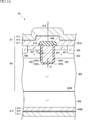
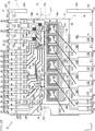
- FIG. 3 is an enlarged cross-sectional view of a main part showing a semiconductor chip of the switch driving device according to the first embodiment. It is a schematic diagram showing a schematic structure of an integrated circuit which constitutes an upper side driver circuit of a switch driver concerning a 1st embodiment.
- FIG. 1 is a schematic diagram showing a motor drive device using a switch drive device according to a first embodiment of the present disclosure.
- the motor drive device MMC shown in the figure drives the motor M.
- Motor M is, for example, a three-phase AC motor.
- the motor M includes a U-phase coil MU, a V-phase coil MV, and a W-phase coil MW described later.
- the coils MU, MV, MW are connected by star connection, but the invention is not limited to this and may be delta connection.
- the motor drive device MMC includes a motor control unit MCU and a power supply unit PS.
- the motor control unit MCU includes a logic circuit (not shown).
- the motor control unit MCU energizes each phase for performing energization control on the coils of each phase (U phase, V phase, W phase) of the motor M at appropriate timing based on the position information of the rotor from the motor M. Generate a control signal. Further, the motor control unit MCU changes the excitation phase switching timing when switching the rotation direction of the motor M, when changing the rotation speed, or the like.
- the power supply unit PS supplies driving power (current) to the coils of each phase of the motor M at the timing based on the energization control signal of each phase received from the motor control unit MCU.
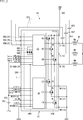
- FIG. 2 is a block diagram of the power supply unit PS including the switch driving device according to the first embodiment.
- the power supply unit PS includes a switch driving device A1 and a bootstrap circuit BTC.
- the switch drive device A1 includes a driver circuit DRV and a power switch circuit PSW.
- the diodes 49U, 49V, 49W forming the driver circuit DRV, the power switch circuit PSW, and the bootstrap circuit BTC are included in one package 7.
- the boot diodes 49U, 49V, 49W are included in the package 7, but the present invention is not limited to this and may be provided outside the package 7.
- the power supply unit PS is connected to the first power supply PW1 and the second power supply PW2.
- the first power supply PW1 supplies the control voltage VCC (for example, 10V to 25V) of the driver circuit DRV.
- the second power supply PW2 supplies a drive voltage VDC (300V, 600V, etc.) for driving the motor M.
- the power switch circuit PSW includes six transistors 4A to 4F (switch elements).
- power MOSFETs are adopted as the six transistors 4A to 4F.
- silicon carbide SiC
- the transistors 4A to 4F are SiC-MOSFETs.
- the transistors 4A to 4F are all N-type MOSFETs.
- the source of the transistor 4A and the drain of the transistor 4D are connected.
- the drain of the transistor 4A is connected to the second power supply PW2.
- the source of the transistor 4D is connected to the ground point. Note that the transistor 4D may be connected to the ground point via a resistance for current detection.
- the U-phase coil MU of the motor M is connected to the connection point between the source of the transistor 4A and the drain of the transistor 4D.
- the transistors 4B and 4E are connected in the same manner as the transistors 4A and 4D.
- the V-phase coil MV of the motor M is connected to a connection point between the source of the transistor 4B and the drain of the transistor 4E.
- the transistor 4C and the transistor 4F are connected similarly to the transistor 4A and the transistor 4D.
- the W-phase coil MW of the motor M is connected to the connection point between the source of the transistor 4C and the drain of the transistor 4F.
- the transistors 4A, 4B, 4C on the second power supply PW2 side of the power switch circuit PSW are referred to as upper transistors (upper switch elements), and the transistors 4D, 4E, 4F on the ground point side are lower transistors (lower switch). Element).
- the driver circuit DRV includes an upper driver chip 4G and a lower driver chip 4H.
- the upper driver chip 4G has a circuit which is connected to the gates of the upper transistors 4A, 4B and 4C and outputs drive signals HU, HV and HW to the respective gates.
- the upper transistors 4A, 4B and 4C are turned on when the voltage levels of the drive signals HU, HV and HW are H level.
- the lower driver chip 4H has a circuit that is connected to the gates of the lower transistors 4D, 4E, and 4F and that inputs drive signals LU, LV, and LW to the respective gates.
- the lower transistors 4D, 4E, 4F are turned ON when the voltage levels of the drive signals LU, LV, LW are H level.
- the voltage level being the H level means that the voltage level is higher than a predetermined voltage.
- the L level indicates that the voltage state is lower than the predetermined voltage.
- the drive voltage VDC of the second power supply PW2 is applied to the U-phase coil MU and the V-phase coil MV. That is, a current flows from the U-phase coil MU to the V-phase coil MV. In this way, the drive signal from the driver circuit DRV switches the ON/OFF timing of the transistors 4A to 4F. As a result, a current is supplied to the coils MU, MV, and MW of each phase at desired timings to excite the coils and rotationally drive the motor M.
- the upper driver chip 4G and the lower driver chip 4H operate by being supplied with the control voltage VCC from the first power supply PW1.
- the upper driver chip 4G and the lower driver chip 4H are connected to the motor control unit MCU, and the energization control signals huin, hvin, hwin,ucin, lvin, lwin are input from the motor control unit MCU.
- the energization control signals huin, hvin, hwin,ucin, lvin, lwin are signals for controlling energization of the transistors 4A to 4F.
- the energization control signals huin, hvin, hwin are input to the upper driver chip 4G, and the energization control signals van, lvin, lwin are input to the lower driver chip 4H.
- the driver circuit DRV inputs the drive signal HU to the gate of the transistor 4A and the drive signal LU to the gate of the transistor 4D.
- the drive signal HV is input to the gate of the transistor 4B, and the drive signal LV is input to the gate of the transistor 4E.
- the drive signal HW is input to the gate of the transistor 4C, and the drive signal LW is input to the gate of the transistor 4F.
- the bootstrap circuit BTC is a circuit that supplies a voltage necessary for driving the upper transistors 4A, 4B, and 4C to the upper driver chip 4G.
- it is a circuit that connects the first power supply PW1 and the source of the upper transistor 4A, and the boot diode 49U and the boot capacitor BC1 are connected in series from the first power supply PW1 side.
- the upper driver chip 4G acquires the voltage at the connection point between the boot diode 49U and the boot capacitor BC1 as the voltage required to drive the upper transistor 4A.
- a resistor for generating a current having a predetermined current value may be arranged between the first power supply PW1 and the boot diode 49U.
- the bootstrap circuit BTC includes a boot diode 49V corresponding to the upper transistor 4B and a boot capacitor BC2, and the upper driver chip 4G acquires the voltage required for driving.
- the bootstrap circuit BTC includes a boot diode 49W corresponding to the upper transistor 4C and a boot capacitor BC3, and the upper driver chip 4G acquires a voltage required for driving.
- the driver circuit DRV of the switch driving device A1 includes a circuit that drives the transistors 4A and 4D, a circuit that drives the transistors 4B and 4E, and a circuit that drives the transistors 4C and 4F.
- the circuits that drive these transistors have the same configuration. Therefore, in the following description, the circuit portion that drives the transistors 4A and 4D will be described as the driver circuit DRV.
- a circuit including the boot diode 49U and the boot capacitor BC1 corresponding to the transistor 4A will be described as a bootstrap circuit BTC.
- the transistor 4A is an upper transistor 4A and the transistor 4D is a lower transistor 4D.
- connection point between the source of the upper transistor 4A and the drain of the lower transistor 4D is referred to as a first point P1
- connection point between the cathode of the boot diode 49U of the bootstrap circuit BTC and the boot capacitor BC1 is referred to as a second point P2.
- FIG. 3 is a block diagram showing a schematic configuration of a driver circuit.
- the driver circuit DRV shown in FIG. 3 includes an upper driver chip 4G and a lower driver chip 4H.
- the lower driver chip 4H has the same configuration as a driver circuit used in a conventionally known switch driving device. Therefore, detailed description of the configuration and operation of the lower driver chip 4H is omitted.
- the upper driver chip 4G includes an upper gate driver 463, an input signal control circuit 464, a current limiting unit 465, a current control unit 466, and a high breakdown voltage level shift circuit 467.
- the input signal control circuit 464 inputs the energization control signal (here, huin) from the motor control unit MCU to the upper gate driver 463 via the high breakdown voltage level shift circuit 467.
- the upper gate driver 463 generates a drive signal HU for driving the upper transistor 4A based on the signal input from the input signal control circuit 464, and outputs it to the gate of the upper transistor 4A.
- the upper gate driver 463 acquires the voltage required to drive the upper transistor 4A from the bootstrap circuit BTC including the boot diode 49U and the boot capacitor BC1.
- the bootstrap circuit BTC charges the boot capacitor BC1 with the current supplied from the first power supply PW1. Both ends of the boot capacitor BC1 are charged to, for example, a voltage equal to or higher than the gate threshold voltage. By doing so, the voltage VB at the second point P2 can be made higher than the voltage VS at the first point P1 by the charging voltage of the boot capacitor BC1 regardless of the voltage VS at the first point P1. it can.
- the upper gate driver 463 acquires the voltage VB at the second point P2, so that the voltage required to drive the upper transistor 4A can be acquired.
- the current limiting unit 465 is provided on the circuit connected from the first power supply PW1 to the boot capacitor BC1.
- the current limiting unit 465 is provided between the cathode of the boot diode 49U and the boot capacitor BC1.
- the current limiting unit 465 limits the current supplied from the first power supply PW1 to the boot capacitor BC1 according to the signal (current limiting signal) from the current control unit 466. In this way, the current limiting unit 465 adjusts (limits) the voltage (charging voltage) across the boot capacitor BC1.
- the detailed configuration of the current limiting unit 465 will be described later.
- FIG. 4 is a timing chart showing the output operation (behavior in mode 2 described later) of the U-phase of the switch driving device A1, and energization control signals huin and van and the voltage VS are shown in order from the top.
- Vsd represents the source-drain voltage of the lower transistor 4D
- Vf represents the forward voltage drop of the parasitic diode associated with the lower transistor 4D.
- the output operation of the V-phase and the W-phase is similar to that of the U-phase, and it suffices to read the energization control signals huin and van in the figure as energization control signals hvin and lvin or energization control signals hwin and lwin, respectively. .. In this figure, the delay time is ignored for the sake of simplicity.
- the upper transistor 4A when the upper transistor 4A is switched from ON to lower transistor 4D as shown at time t2 to t3, time t4 to t5, time t6 to t7, and time t8 to t9, the upper transistor 4A is turned on.
- the switch driving device A1 that operates as described above, by turning on the upper transistor 4A and turning off the lower transistor 4D, a voltage is applied from the second power source PW2 to the U-phase coil MU which is a load (that is, , Supplied with current).
- the voltage VS at the first point P1 may be substantially the same as the drive voltage VDC of the second power source PW2 (that is, about 300V).
- the voltage VB at the second point P2 to which the upper gate driver 463 is connected is smaller than the voltage VS at the first point P1 by the voltage across the boot capacitor BC1 (hereinafter, charging voltage VBS). Only high voltage. For example, when the voltage VS at the first point P1 changes from 0V to 300V and the charging voltage of the boot capacitor BC1 is 18V, the voltage VB at the second point P2 changes from about 18V to 318V.
- the upper gate driver 463 can always obtain a voltage capable of driving the upper transistor 4A.
- the boot capacitor BC1 serves as a floating power supply.
- the boot capacitor BC1 has a configuration capable of being charged to a voltage higher than the gate threshold voltage.
- the current limiting unit 465 will not be provided.
- the switch driving device A1 the case where the motor current flows in the forward direction of the lower transistor 4D is referred to as mode 1, and the case where the body diode of the lower transistor 4D is turned on (during lower regeneration) is referred to as mode 2.
- the boot capacitor BC1 is charged in mode 1 and mode 2.
- the motor current IM flows from the neutral point of the motor M to the ground terminal via the first point P1 and the lower transistor 4D in the U-phase coil MU.
- the voltage VS at the first point P1 becomes the same or substantially the same voltage (0 V) as the ground potential.
- IM ⁇ R since there is a resistance component R due to the ON resistance of the lower transistor 4D and the current detection resistance, only IM ⁇ R has a voltage higher than 0V. Therefore, the voltage across the boot capacitor BC1 is substantially the same as the control voltage VCC of the first power supply PW1, and in this state, the boot capacitor BC1 is charged to the voltage VCC.
- VBS VCC- It becomes VFBOOT-Ron ⁇ IM.
- charging is performed when the voltage VB at the second point P2 becomes equal to or lower than the charging voltage VBS described above.
- the upper transistor 4A and the lower transistor 4D include a parasitic diode (body diode).
- the forward voltage drop due to the parasitic diode of the lower transistor 4D is Vf.
- the motor M is regeneratively operated in the mode 2
- the motor current flows through the U-phase coil MU from the first point P1 toward the neutral point.
- the upper transistor 4A is OFF
- no current flows from the second power supply PW2.
- the lower transistor 4D is OFF, current flows through the parasitic diode. Therefore, the voltage VS at the first point P1 becomes ⁇ Vf, which is lower than the ground voltage.
- the charging voltage VBS of the boot capacitor BC1 is higher in the mode 2 than in the mode 1.
- the voltage across the boot capacitor BC1 may be higher than the allowable gate-source voltage (assumed to be the allowable gate voltage) in the upper transistor 4A. If the voltage (VCC+Vf) across the boot capacitor BC1 becomes higher than the allowable gate voltage, it may cause deterioration or damage of the upper transistor 4A.
- the overcharged state refers to, for example, a state in which the charging voltage VBS of the boot capacitor BC1 is charged to a voltage higher than the allowable gate voltage of the upper transistor 4A.
- the SiC-based transistor since the SiC-based transistor has a high forward drop voltage Vf of the parasitic diode associated therewith, it is likely to cause an overcharged state.
- the upper driver chip 4G includes a current limiting unit 465 in the circuit from the boot diode 49U to the boot capacitor BC1.
- the current limiting unit 465 limits the current supplied to the boot capacitor BC1 and controls the boot capacitor BC1 so as not to be overcharged.
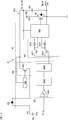
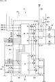
- FIG. 5 is a circuit diagram of an example of the upper driver chip 4G used in the switch driving device A1.
- the overcharged state of the boot capacitor BC1 occurs because the voltage (VCC+Vf) across the boot capacitor BC1 becomes too large.
- the switch driver A1 has a configuration in which the upper driver chip 4G does not overcharge the boot capacitor BC1 even when different power supply voltages are connected.
- the upper driver chip 4G includes an upper gate driver 463, an input signal control circuit 464, a current limiting unit 465, a current control unit 466, and a high breakdown voltage level shift circuit 467.
- the current control unit 466 sends a signal to the current limiting unit 465 to drive the current limiting unit 465 and generate a voltage drop between the boot diode 49U and the boot capacitor BC1 to charge the boot capacitor BC1.
- the current limiting unit 465 limits the current that charges the boot capacitor BC1.
- the energization control signal huin is input to the input signal control circuit 464 from the motor control unit MCU (see FIG. 1 etc.).
- the input signal control circuit 464 includes an inverter (Schmitt buffer) 4641 that converts the energization control signal huin into an L signal or an H signal.
- the input signal control circuit 464 includes a level shift circuit 4642 and a pulse generator 4643.
- the level shift circuit 4642 has a function of increasing the voltage level of the signal output from the inverter 4641. This facilitates handling of signals in the upper driver chip 4G.
- the pulse generator 4643 has a function of outputting a set pulse signal and a reset pulse signal based on the signal output from the level shift circuit 4642.
- the set pulse signal and the reset pulse signal output from the pulse generator 4643 are input to the high breakdown voltage level shift circuit 467.
- the high breakdown voltage level shift circuit 467 includes a transistor 4671, a transistor 4672, a resistor 4673, and a resistor 4674.
- the transistors 4671 and 4672 are N-type MOSFETs and are high breakdown voltage transistors.
- the drain of the transistor 4671 is connected to the second point P2 or a point having the same potential as the second point P2 through the resistor 4673.
- the source of the transistor 4671 is connected to the ground point via a resistor (not shown), and the pulse signal from the pulse generator 4643 is input to the gate.
- the drain of the transistor 4672 is connected to the second point P2 or a point having the same potential as the second point P2 through the resistor 4674.
- the source of the transistor 4672 is connected to the ground point via a resistor (not shown), and the pulse signal from the pulse generator 4643 is input to the gate.
- connection point between the drain of the transistor 4671 and the resistor 4673 and the connection point between the drain of the transistor 4672 and the resistor 4674 respectively set the input signal level to the inverter (not shown) forming the input stage of the upper gate driver 463 to a predetermined value. It is connected to a clamp circuit 4631 (see FIG. 15) that limits the following.
- the signal lines of the set pulse signal and the reset pulse signal are laid so as to be symmetrical to each other.
- the length (for example, the length of the reset pulse signal wiring) is the same or substantially the same.
- the element arrangement of the pair of the transistor 4671 and the resistor 4673 and the pair of the transistor 4672 and the resistor 4674 are symmetrical to each other. By doing so, the wiring resistance and the parasitic capacitance are the same, and the deviation of the signal from each wiring is suppressed.
- the current limiting unit 465 includes a transistor 4651.
- the transistor 4651 is arranged in a path connecting the boot diode 49U and the boot capacitor BC1 and is arranged in a region having the same potential as the boot capacitor BC1 which is a floating power supply.
- the transistor 4651 is a P-type MOSFET.
- the source of the transistor 4651 is connected to the cathode of the boot diode 49U.
- the drain of the transistor 4651 is connected to the boot capacitor BC1.
- a signal from the current controller 466 is input to the gate of the transistor 4651.
- the current control unit 466 detects the voltage VB at the second point P2.
- the current control unit 466 also compares the detected voltage VB with a preset threshold voltage. When the voltage VB is equal to or higher than the threshold voltage, the current control unit 466 outputs an H level signal to the gate of the transistor 4651. This turns off the transistor 4651. On the other hand, the current controller 466 outputs an L level signal to the gate of the transistor 4651 when the voltage VB is lower than the threshold voltage. This turns on the transistor 4651.
- the current control unit 466 can be realized by changing the threshold voltage of a conventionally known OVLO circuit, for example, and detailed description thereof will be omitted.
- the transistor 4651 When the voltage VB is equal to or higher than the threshold voltage, the transistor 4651 is turned off based on the signal from the current control unit 466. Therefore, the conduction path between the boot diode 49U and the boot capacitor BC1 is cut off. On the other hand, when the voltage VB is lower than the threshold voltage, the transistor 4651 is turned on based on the signal from the current control unit 466. Therefore, the conduction path between the boot diode 49U and the boot capacitor BC1 is secured. That is, when the voltage VB is equal to or higher than the threshold voltage, the boot capacitor BC1 is not charged. On the contrary, when the voltage VB is lower than the threshold voltage, current flows between the boot diode 49U and the boot capacitor BC1 and the boot capacitor BC1 is charged.
- the illustrated switch driving device A1 includes a plurality of leads 1, a plurality of leads 2, a substrate 3, a plurality of transistors 4, a plurality of driver chips 4, a plurality of boot diodes 49, a conductive part 5, a plurality of joint parts 6, and a plurality of parts.
- the first wire 91, the plurality of second wires 92, and the package 7 are provided.
- the switch drive device A1 can be used, for example, in a drive circuit that drives a compressor of an outdoor unit of an air conditioner, a drive circuit that drives a compressor of a refrigerator, a drive circuit that drives a fan, and the like.
- the drive circuit drives, for example, a three-phase AC motor.
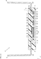
- FIG. 6 is a perspective view showing the switch driving device A1.
- FIG. 7 is a plan view showing the switch driving device A1.
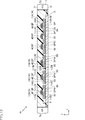
- FIG. 8 is a bottom view showing the switch driving device A1.
- FIG. 9 is a main part plan view showing the switch driving device A1.
- FIG. 10 is an enlarged plan view of an essential part showing the switch driving device A1.
- FIG. 11 is an enlarged plan view of an essential part showing the substrate of the switch driving device A1.
- FIG. 12 is a sectional view taken along line XII-XII in FIG.
- FIG. 13 is a sectional view taken along line XIII-XIII in FIG.
- FIG. 14 is an enlarged sectional view of an essential part showing a transistor of the switch driving device A1.
- the z direction corresponds to the thickness direction of the substrate 3.
- the x direction (first direction) is a direction perpendicular to the z direction.
- the y direction is a direction perpendicular to the z direction and the x direction.
- the material forming the substrate 3 is not particularly limited.
- a material of the substrate 3 for example, a material having a higher thermal conductivity than that of the resin 7 is preferable.
- the material of the substrate 3 include ceramics such as alumina (Al 2 O 3 ), silicon nitride (SiN), aluminum nitride (AlN), and alumina containing zirconia.
- the thickness of the substrate 3 is not particularly limited and is, for example, about 0.1 mm to 1.0 mm.
- the shape of the substrate 3 is not particularly limited, and various shapes can be used.
- the substrate 3 has a first surface 31, a second surface 32, a third surface 33, a fourth surface 34, a fifth surface 35 and a sixth surface 36.
- the first surface 31 faces the z direction.
- the second surface 32 faces the side opposite to the first surface 31.
- the third surface 33 is located between the first surface 31 and the second surface 32 in the z direction, and is connected to the first surface 31 and the second surface 32.
- the third surface 33 faces the x direction.
- the fourth surface 34 is located between the first surface 31 and the second surface 32 in the z direction, and is connected to the first surface 31 and the second surface 32.
- the fourth surface 34 faces the side opposite to the third surface 33.
- the fifth surface 35 is located between the first surface 31 and the second surface 32 in the z direction, and is connected to the first surface 31 and the second surface 32.
- the fifth surface 35 faces the y direction.
- the sixth surface 36 is located between the first surface 31 and the second surface 32 in the z direction and is connected to the first surface 31 and the second surface 32.
- the sixth surface 36 faces the side opposite to the fifth surface 35.
- the substrate 3 has a rectangular shape when viewed in the z direction.
- the substrate 3 is elongated in the x direction when viewed in the z direction.
- the conductive portion 5 is formed on the substrate 3. In the example shown in the drawing, the conductive portion 5 is formed on the first surface 31 of the substrate 3.
- the conductive portion 5 is made of a conductive material.
- the conductive material forming the conductive portion 5 is not particularly limited, but examples thereof include silver (Ag), copper (Cu), and gold (Au). In the following description, the case where the conductive portion 5 contains silver will be described as an example.
- the conductive portion 5 may include Ag—Pt or Ag—Pd.
- the conductive portion 5 is formed, for example, by firing a paste containing these metals, but the present disclosure is not limited to this.
- the thickness of the conductive portion 5 is not particularly limited and is, for example, about 5 ⁇ m to 30 ⁇ m.
- the shape (pattern) of the conductive portion 5 is not particularly limited, and includes, for example, at least one wiring portion (first wiring portion, second wiring portion, etc.), at least one base portion, and at least one connection portion. ..
- the conductive portion 5 includes a plurality of wiring portions 50A to 50P, a plurality of wiring portions 50U to 50W, a first base portion 55, a second base portion 56, and a connection portion 57.
- the wiring parts 50U to 50W are examples of the “first wiring part”
- the wiring parts 50A to 50C are examples of the “second wiring part”.
- the shape of the first base 55 is not particularly limited and is, for example, a rectangular shape, a polygonal shape, a circular shape, or an elliptical shape.
- the first base 55 is a rectangle elongated in the x direction.
- the shape of the second base portion 56 is not particularly limited and is, for example, a rectangular shape, a polygonal shape, a circular shape, or an elliptical shape.
- the second base portion 56 is a rectangle elongated in the x direction.
- the connecting portion 57 is interposed between the first base portion 55 and the second base portion 56, and in the illustrated example, connects the first base portion 55 and the second base portion 56 to each other.
- the shape of the connecting portion 57 is not particularly limited, and may be, for example, linear or non-linear (bent or curved as a whole).
- each of the first base portion 55, the second base portion 56, and the connecting portion 57 has a first side and a second side that are separated from each other in the y direction (second side). Is closer to the sixth surface 36 than the first side).
- the second sides (three sides) of each of the first base portion 55, the second base portion 56, and the connecting portion 57 are aligned with each other along the x direction, and form one straight line segment. (The above three sides are at the same position in the y direction).
- the wiring section 50A is composed of, for example, a first section 51A, a second section 52A, and a third section 53A.
- the shape of the first portion 51A is not particularly limited and is, for example, a rectangular shape, a polygonal shape, a circular shape, or an elliptical shape.
- the first portion 51A is a rectangle elongated in the x direction.
- the first portion 51A is arranged apart from the first base 55 on the third surface 33 side in the x direction.
- the first portion 51A overlaps a part of the first base 55 when viewed in the x direction.
- the second portion 52A is arranged closer to the fifth surface 35 than the first portion 51A in the y direction.
- the shape of the second portion 52A is not particularly limited and is, for example, a rectangular shape, a polygonal shape, a circular shape, or an elliptical shape.
- the second portion 52A has a rectangular shape and is elongated in the y direction.
- the third part 53A is interposed between the first part 51A and the second part 52A, and is connected to the first part 51A and the second part 52A in the illustrated example.
- the shape of the third portion 53A is not particularly limited, and in the illustrated example, the third portion 53A has a rectangular shape (strip shape) extending in the y direction.
- the wiring section 50B is composed of a first section 51B and a second section 52B.
- the shape of the first portion 51B is not particularly limited and is, for example, a rectangular shape, a polygonal shape, a circular shape, or an elliptical shape.
- the first portion 51B has a rectangular shape extending in the y direction.
- the first portion 51B is arranged apart from the first base 55 on the fifth surface 35 side in the y direction.
- the first portion 51B is arranged apart from the first portion 51A on the fourth surface 34 side in the x direction.
- the second portion 52B is arranged closer to the fifth surface 35 than the first portion 51B in the y direction.
- the second portion 52B is arranged apart from the second portion 52A on the fourth surface 34 side in the x direction.
- the shape of the second portion 52B is not particularly limited and is, for example, a rectangular shape, a polygonal shape, a circular shape, or an elliptical shape.
- the second portion 52B is a rectangle elongated in the x direction.
- the first part 51B and the second part 52B are connected to each other.
- the wiring section 50C is composed of a first section 51C and a second section 52C.
- the shape of the first portion 51C is not particularly limited and is, for example, a rectangular shape, a polygonal shape, a circular shape, or an elliptical shape.
- the first portion 51C has a rectangular shape extending in the y direction.
- the first portion 51C is arranged apart from the first base 55 on the fifth surface 35 side in the y direction.
- the first portion 51C is arranged apart from the first portion 51B on the fourth surface 34 side in the x direction.
- the first portion 51C overlaps the first portion 51B when viewed in the x direction.
- the second portion 52C is arranged closer to the fifth surface 35 than the first portion 51C in the y direction.
- the second portion 52C is arranged apart from the second portion 52B on the fourth surface 34 side in the x direction.
- the shape of the second portion 52C is not particularly limited and is, for example, a rectangular shape, a polygonal shape, a circular shape, or an elliptical shape.
- the first portion 51C and the second portion 52C are connected to each other.
- the wiring unit 50U is separated from the wiring unit 50A and is arranged adjacent to a part of the wiring unit 50A.
- the shape of the wiring portion 50U is not particularly limited and is, for example, a rectangular shape, a polygonal shape, a circular shape, or an elliptical shape. In the illustrated example, the wiring portion 50U has a rectangular shape.
- the wiring portion 50U is arranged on the fifth surface 35 side in the y direction with respect to the first portion 51A of the wiring portion 50A.
- the wiring part 50V is separated from the wiring part 50B and is arranged adjacent to a part of the wiring part 50B.
- the shape of the wiring portion 50V is not particularly limited and is, for example, a rectangular shape, a polygonal shape, a circular shape, or an elliptical shape. In the illustrated example, the wiring portion 50V has a rectangular shape.
- the wiring portion 50V is arranged on the third surface 33 side in the x direction with respect to the first portion 51B of the wiring portion 50B. Further, the wiring portion 50V is arranged apart from the wiring portion 50U on the fourth surface 34 side in the x direction.
- the wiring portion 50W is separated from the wiring portion 50C, and is arranged adjacent to a part of the wiring portion 50C.
- the shape of the wiring portion 50W is not particularly limited and is, for example, a rectangular shape, a polygonal shape, a circular shape, or an elliptical shape. In the illustrated example, the wiring portion 50W has a rectangular shape.
- the wiring portion 50W is arranged on the fourth surface 34 side in the x direction with respect to the first portion 51C of the wiring portion 50C.
- the wiring portion 50W is arranged on the side of the fourth surface 34 so as to be spaced from the wiring portion 50V in the x direction with the first portion 51B and the first portion 51C interposed therebetween.
- the wiring parts 50D to 50G are arranged on the fourth surface 34 side in the x direction with respect to the wiring part 50W. In FIG. 11, the wiring parts 50D to 50G are arranged in this order.
- Each of the wiring portions 50D to 50G has two rectangular pad-shaped portions and a bent strip-shaped portion that connects these pad-shaped portions.
- the wiring portion 50H is connected to the second base portion 56 and extends from the second base portion 56 toward the fifth surface 35 in the y direction.
- the wiring portion 50H has a pad-shaped portion.
- the wiring portions 50I to 50N are arranged on the fourth surface 34 side with respect to the wiring portion 50H in the x direction, and are arranged in this order.
- Each of the wiring portions 50I to 50N has a pad-shaped portion located on the second base 56 side, a pad-shaped portion located on the fifth surface 35 side, and a strip-shaped portion connecting these pad-shaped portions.
- the wiring portion 50O is connected to the second base portion 56 and extends from the second base portion 56 in a direction inclined with respect to the x direction.
- the wiring portion 50O has a pad-shaped portion located on the fourth surface 34 side and a strip-shaped portion connecting the pad upper portion and the second base portion 56.
- the wiring portion 50P is located on the sixth surface 36 side in the y direction with respect to the wiring portion 50O, and is located on the fourth surface 34 side in the x direction with respect to the second base 56.
- the wiring portion 50P has a pad-shaped portion located on the fourth surface 34 side, a pad-shaped portion located on the second base portion 56 side, and a strip-shaped portion connecting these pad-shaped portions.
- the substrate 3 shown in FIG. 11 has, for example, two regions adjacent to each other in the y direction, that is, a first region 30A and a second region 30B.
- the first area 30A is near the sixth surface 36, and the second area 30B is near the fifth surface 35.
- the wiring portions 50A to 50P and 50U to 50W described above are provided in the second region 30B.
- the plurality of joint portions 6 are formed on the substrate 3.
- the plurality of joint portions 6 are formed on the first surface 31 of the substrate 3.
- the material of the joining portion 6 is not particularly limited, and is made of, for example, a material capable of joining the substrate 3 and the lead 1.
- the joint portion 6 is made of, for example, a conductive material.
- the conductive material forming the joint 6 is not particularly limited. Examples of the conductive material of the joint portion 6 include materials containing silver (Ag), copper (Cu), gold (Au), and the like. In the following description, the case where the bonding portion 6 contains silver will be described as an example.
- the joint portion 6 in this example includes the same conductive material as the conductive portion 5.
- the joint portion 6 may include copper in place of silver, or may include gold in place of silver or copper.
- the conductive portion 5 may include Ag—Pt or Ag—Pd.
- the method of forming the joint portion 6 is not limited, and for example, similar to the conductive portion 5, the joint portion 6 is formed by firing a paste containing these metals.
- the thickness of the joint portion 6 is not particularly limited and is, for example, about 5 ⁇ m to 30 ⁇ m.
- the plurality of joints 6 includes joints 6A to 6D.
- the joint portion 6A is arranged closer to the sixth surface 36 than the conductive portion 5 in the y direction.
- the joint portion 6A overlaps all of the first base portion 55 when viewed in the y direction.
- the shape of the joint 6A is not particularly limited.
- the joint portion 6B is arranged closer to the sixth surface 36 than the conductive portion 5 in the y direction.
- the joint portion 6B is arranged closer to the fourth surface 34 than the joint portion 6A in the x direction.
- the joint portion 6B overlaps the connecting portion 57 and the second base portion 56 when viewed in the y direction.
- the shape of the joint 6B is not particularly limited.
- the joint portion 6C is arranged closer to the sixth surface 36 side than the conductive portion 5 in the y direction.
- the joint portion 6C is arranged closer to the fourth surface 34 than the joint portion 6B in the x direction.
- the joint portion 6C entirely overlaps the second base portion 56 when viewed in the y direction.
- the shape of the joint 6C is not particularly limited.
- the joint portion 6D is arranged closer to the sixth surface 36 than the conductive portion 5 in the y direction.
- the joint portion 6D is arranged closer to the fourth surface 34 than the joint portion 6C in the x direction.
- the joint portion 6D overlaps the second base portion 56, the wiring portion 50O, and the wiring portion 50P when viewed in the y direction.
- the shape of the joint 6D is not particularly limited.
- the joint portions 6A to 6D are formed in the area of the substrate 3 closer to the sixth surface 36 than the conductive portion 5 in the y direction.
- the region on the sixth surface 36 side of the substrate 3 where the bonding portion 6 is formed is defined as the first region 30A.
- the plurality of leads 1 are configured to include a metal, and have better heat dissipation characteristics than the substrate 3, for example.
- the metal forming the lead 1 is not particularly limited, and includes, for example, copper (Cu), aluminum, iron (Fe), oxygen-free copper, or alloys thereof (eg, Cu—Sn alloy, Cu—Zr alloy, Cu—Fe alloy). Etc.). Further, the plurality of leads 1 may be plated with nickel (Ni).
- the plurality of leads 1 may be formed by, for example, press work of pressing a die against a metal plate, or may be formed by patterning the metal plate by etching, but the present invention is not limited to this.
- the thickness of the lead 1 is not particularly limited and is, for example, about 0.4 mm to 0.8 mm.
- the plurality of leads 1 include a plurality of leads 1A to 1G and 1Z in the examples shown in FIGS. 6 to 9.
- the plurality of leads 1A to 1G form a conduction path to the transistors 4A to 4F, for example.
- the leads 1A to 1D are respectively arranged on the substrate 3, and in the example shown in the figure, they are arranged on the first surface 31.
- the lead 1A is bonded to the bonding portion 6A via the bonding material 81.
- the bonding material 81 may be any material that can bond the lead 1A to the bonding portion 6A. From the viewpoint of efficiently transmitting the heat from the lead 1A to the substrate 3, it is preferable that the bonding material 81 has a higher thermal conductivity, and for example, silver paste, copper paste, solder or the like is used. However, the bonding material 81 may be an insulating material such as an epoxy resin or a silicone resin. Further, when the bonding portion 6A is not formed on the substrate 3, the lead 1A may be bonded to the substrate 3.
- the structure of the lead 1A is not particularly limited, and in the example shown in the figure, the lead 1A is composed of a first part 11A, a second part 12A, a third part 13A and a fourth part 14A.
- the first portion 11A has a main surface 111A, a back surface 112A, and a plurality of recesses 1111A.
- the main surface 111A is a surface facing the same side as the first surface 31 in the z direction.
- the back surface 112A is a surface facing away from the main surface 111A in the z direction, and is a flat surface in the illustrated example.
- the back surface 112A is joined to the joining portion 6A by a joining material 81, as shown in FIGS. 12 and 13.
- the plurality of recesses 1111A are recessed in the z direction from the main surface 111A.
- the shape of the recess 1111A as viewed in the z direction is not particularly limited, and may be, for example, a circle, an ellipse, a rectangle, or a triangle.
- the plurality of recesses 1111A are arranged in a matrix.
- the third part 13A and the fourth part 14A are covered by the package 7.
- the third portion 13A is connected to the first portion 11A and the fourth portion 14A.
- the third portion 13A is connected to the portion of the first portion 11A between the fourth surface 124Aa and the eighth surface 124Ab.
- the third portion 13A overlaps the sixth surface 36 when viewed in the z direction.
- the fourth portion 14A is located in the z direction with a shift from the first portion 11A toward the side toward which the main surface 111A faces.
- the end of the fourth portion 14A is flush with the sixth surface 76 of the resin 7.
- the second portion 12A is a portion that is connected to the end of the fourth portion 14A and projects from the package 7 of the lead 1A.
- the second portion 12A projects to the side opposite to the first portion 11A in the y direction.
- the second portion 12A is used to electrically connect the switch driving device A1 to an external circuit, for example.
- the second portion 12A is bent in the z direction so that the main surface 111A faces the side.
- the lead 1B is joined to the joining portion 6B via the joining material 81 described above.
- the lead 1B may be bonded to the substrate 3 when the bonding portion 6B is not formed on the substrate 3.
- the structure of the lead 1B is not particularly limited, and in the example shown in the figure, the lead 1B is composed of a first part 11B, a second part 12B, a third part 13B and a fourth part 14B.
- the first portion 11B has a main surface 111B, a back surface 112B, and a plurality of recesses 1111B.
- the main surface 111B is a surface facing the same side as the first surface 31 in the z direction.
- the back surface 112B is a surface facing away from the main surface 111B in the z direction, and is a flat surface in the illustrated example. As shown in FIG. 13, the back surface 112B is joined to the joining portion 6B by the joining material 81.
- the plurality of recesses 1111B are recessed from the main surface 111B in the z direction.
- the shape of the recess 1111B viewed in the z direction is not particularly limited and may be, for example, a circle, an ellipse, a rectangle, a triangle, or the like. Further, in the illustrated example, the plurality of recesses 1111B are arranged in a matrix.
- the third part 13B and the fourth part 14B are covered with the package 7.
- the third portion 13B is connected to the first portion 11B and the fourth portion 14B.
- the third portion 13B is connected to a portion of the first portion 11B adjacent to the fourth surface 124B.
- the third portion 13B overlaps with the sixth surface 36 when viewed in the z direction.
- the fourth portion 14B is located in the z direction with a shift from the first portion 11B toward the side toward which the main surface 111B faces.
- the end of the fourth portion 14B is flush with the sixth surface 76 of the resin 7.
- the second portion 12B is a portion that is connected to the end of the fourth portion 14B and projects from the package 7 of the lead 1B.
- the second portion 12B projects to the side opposite to the first portion 11B in the y direction.
- the second portion 12B is used, for example, to electrically connect the switch driving device A1 to an external circuit.
- the second portion 12B is bent in the z direction so that the main surface 111B faces.
- the lead 1C is bonded to the bonding portion 6C via the bonding material 81 described above. If the bonding portion 6C is not formed on the substrate 3, the lead 1C may be bonded to the substrate 3.
- the structure of the lead 1C is not particularly limited, and in the example shown in FIG. 9, the lead 1C is composed of a first part 11C, a second part 12C, a third part 13C and a fourth part 14C.
- the first portion 11C has a main surface 111C, a back surface 112C, and a plurality of recesses 1111C.
- the main surface 111C is a surface facing the same side as the first surface 31 in the z direction.
- the back surface 112C is a surface facing away from the main surface 111C in the z direction, and is a flat surface in the illustrated example. As shown in FIG. 13, the back surface 112C is joined to the joining portion 6C by the joining material 81.
- the plurality of recesses 1111C are recessed in the z direction from the main surface 111C.
- the shape of the recess 1111C as viewed in the z direction is not particularly limited, and may be, for example, a circle, an ellipse, a rectangle, a triangle, or the like. Further, in the illustrated example, the plurality of recesses 1111C are arranged in a matrix.
- the third part 13C and the fourth part 14C are covered by the package 7.
- the third portion 13C is connected to the first portion 11C and the fourth portion 14C.
- the third portion 13C is connected to a portion of the first portion 11C that is adjacent to the fourth surface 124C.
- the third portion 13C overlaps the sixth surface 36 when viewed in the z direction.
- the fourth portion 14C is located in the z-direction offset from the first portion 11C toward the side on which the main surface 111C faces, and is connected to the second portion 12C.
- the end of the fourth portion 14C is flush with the sixth surface 76 of the resin 7.
- the second portion 12C is a portion of the lead 1C that is connected to the end portion of the fourth portion 14C and projects from the package 7.
- the second portion 12C projects to the side opposite to the first portion 11C in the y direction.
- the second portion 12C is used to electrically connect the switch driving device A1 to an external circuit, for example.
- the second portion 12C is bent in the z direction so that the main surface 111C faces the side.
- the lead 1D is bonded to the bonding portion 6D via the bonding material 81 described above.
- the lead 1D may be bonded to the substrate 3 when the bonding portion 6D is not formed on the substrate 3.
- the structure of the lead 1D is not particularly limited, and in the example shown in FIG. 9, the lead 1D is composed of a first part 11D, a second part 12D, a third part 13D and a fourth part 14D.
- the first portion 11D has a main surface 111D, a back surface 112D, and a plurality of recesses 1111D.
- the main surface 111D is a surface facing the same side as the first surface 31 in the z direction.
- the back surface 112D is a surface facing the side opposite to the main surface 111D in the z direction, and is a flat surface in the illustrated example. As shown in FIG. 13, the back surface 112D is bonded to the bonding portion 6D by the bonding material 81.
- the plurality of recesses 1111D are recessed in the z direction from the main surface 111D.
- the shape of the recess 1111D as viewed in the z direction is not particularly limited, and may be, for example, a circle, an ellipse, a rectangle, a triangle, or the like.
- the plurality of recesses 1111D are arranged in a matrix.
- the third part 13D and the fourth part 14D are connected to the first part 11D and the fourth part 14D.
- the third portion 13D is connected to a portion of the first portion 11D that is adjacent to the fourth surface 124D.
- the third portion 13D overlaps the sixth surface 36 when viewed in the z direction. It is covered by the package 7.
- the fourth portion 14D is located in the z-direction and is displaced from the first portion 11D toward the side on which the main surface 111D faces, and is connected to the second portion 12D.
- the end of the fourth portion 14D is flush with the sixth surface 76 of the resin 7.
- the second portion 12D is a portion that is connected to the end portion of the fourth portion 14D and projects from the package 7 in the lead 1D.
- the second portion 12D projects to the side opposite to the first portion 11D in the y direction.
- the second portion 12D is used, for example, to electrically connect the switch driving device A1 to an external circuit.
- the second portion 12D is bent in the z direction so that the main surface 111D faces the side.
- the lead 1E is separated from the substrate 3 when viewed in the z direction.
- the lead 1E is arranged on the side facing the sixth surface 36 with respect to the substrate 3 in the y direction.
- the structure of the lead 1E is not particularly limited, and in the example shown in FIG. 9, the lead 1E is composed of the second part 12E and the fourth part 14E.
- the fourth part 14E is covered by the package 7. Similar to the fourth portion 14D in the lead 1D, the fourth portion 14E is located in the z direction with a shift from the first portion 11D toward the side where the main surface 111D faces. The fourth portion 14E overlaps the first portion 11D when viewed in the y direction. The end of the fourth portion 14E is flush with the sixth surface 76 of the resin 7.
- the second portion 12E is a portion that is connected to the end portion of the fourth portion 14E and projects from the package 7 in the lead 1E.
- the second portion 12E projects to the side opposite to the fourth portion 14E in the y direction.
- the second portion 12E is used, for example, to electrically connect the switch driving device A1 to an external circuit.
- the second portion 12E is bent in the z direction so that the first surface 31 faces.
- the lead 1F is separated from the substrate 3 when viewed in the z direction.
- the lead 1F is arranged on the side facing the sixth surface 36 with respect to the substrate 3 in the y direction. Further, the lead 1F is arranged on the opposite side of the lead 1E from the fourth portion 14D in the x direction.
- the structure of the lead 1F is not particularly limited, and in the example shown in FIG. 9, the lead 1F is composed of the second part 12F and the fourth part 14F.
- the fourth part 14F is covered by the package 7. Similarly to the fourth portion 14D in the lead 1D, the fourth portion 14F is located in the z direction with a shift from the first portion 11D toward the side toward which the main surface 111D faces. The fourth portion 14F overlaps the first portion 11D when viewed in the y direction. The end of the fourth portion 14F is flush with the sixth surface 76 of the resin 7.
- the second portion 12F is a portion connected to the end of the fourth portion 14F and protruding from the package 7 in the lead 1F.
- the second portion 12F projects to the side opposite to the fourth portion 14F in the y direction.
- the second portion 12F is used, for example, to electrically connect the switch driving device A1 to an external circuit.
- the second portion 12F is bent so that the first surface 31 faces in the z direction.
- the lead 1G is separated from the substrate 3 when viewed in the z direction.
- the lead 1G is arranged on the side facing the fourth surface 34 with respect to the substrate 3 in the x direction. Further, the lead 1G is arranged on the opposite side of the lead 1E from the fourth portion 14D in the x direction.
- the structure of the lead 1G is not particularly limited, and in the example shown in FIG. 9, the lead 1G is composed of the second part 12G and the fourth part 14G.
- the fourth part 14G is covered by the package 7. Similar to the fourth portion 14D in the lead 1D, the fourth portion 14G is located in the z direction with a shift from the first portion 11D toward the side toward which the main surface 111D faces. The fourth portion 14G overlaps the fourth portion 14F when viewed in the y direction. The end of the fourth portion 14G is flush with the sixth surface 76 of the resin 7.
- the second portion 12G is a portion connected to the end of the fourth portion 14G and protruding from the package 7 in the lead 1G.
- the second portion 12G projects to the side opposite to the fourth portion 14G in the y direction.
- the second portion 12G is used for electrically connecting the switch driving device A1 to an external circuit, for example.
- the second portion 12G is bent in the z direction so that the first surface 31 faces.
- the lead 1Z is separated from the substrate 3 when viewed in the z direction.
- the lead 1Z is arranged closer to the third surface 33 than the substrate 3 in the x direction. Further, the lead 1Z is arranged on the side opposite to the lead 1B with respect to the lead 1A in the x direction.
- the structure of the lead 1Z is not particularly limited, and in the example shown in FIG. 9, the lead 1Z is composed of the second portion 12Z and the fourth portion 14Z. Further, the lead 1Z is insulated from the circuit of the switch driving device A1.
- the fourth part 14Z is covered by the package 7. Similar to the fourth portion 14D in the lead 1D, the fourth portion 14Z is located shifted in the z direction from the first portion 11D so that the main surface 111D faces the side.
- the shape of the fourth portion 14Z is not particularly limited, and in the illustrated example, it is a strip shape extending in the y direction. The end of the fourth portion 14Z is flush with the sixth surface 76 of the resin 7.
- the second portion 12Z is a portion that is connected to the end portion of the fourth portion 14Z and projects from the package 7 in the lead 1Z.
- the second portion 12Z projects to the side opposite to the fourth portion 14Z in the y direction.
- the second portion 12Z is used, for example, when mounting the switch driving device A1 on an external circuit board.
- the second portion 12Z is bent in the z direction so that the first surface 31 faces.
- the second portion 12A, the second portion 12B, the second portion 12C, and the second portion 12D are arranged with a gap G11 in the x direction. These gaps G11 have substantially the same length.
- the second portion 12D and the second portion 12E are arranged with a gap G12 in the x direction.
- the gap G12 has substantially the same length as the gap G11.
- the second portion 12E, the second portion 12F, and the second portion 12G are arranged with a gap G13 in the x direction. The length of these gaps G13 is shorter than the gap G11.
- the second portion 12A and the second portion 12Z are arranged with a gap G14 in the x direction.
- the gap G14 is larger than the gap G11.
- the plurality of leads 2 are configured to include metal, and have better heat dissipation characteristics than the substrate 3, for example.
- the metal forming the lead 2 is not particularly limited, and includes, for example, copper (Cu), aluminum, iron (Fe), oxygen-free copper, or alloys thereof (eg, Cu—Sn alloy, Cu—Zr alloy, Cu—Fe alloy). Etc.). Further, the plurality of leads 2 may be plated with nickel (Ni).
- the plurality of leads 2 may be formed, for example, by pressing a metal plate against a metal plate, or may be formed by patterning the metal plate by etching, but the present invention is not limited to this.
- the thickness of the lead 2 is not particularly limited and is, for example, about 0.4 mm to 0.8 mm.
- the plurality of leads 2 are arranged so as to overlap the second region 30B of the substrate 3 when viewed in the z direction.
- the plurality of leads 2 include a plurality of leads 2A to 2P and 2Z in the examples shown in FIGS. 6 to 9.
- the plurality of leads 2A to 2O form a conduction path to the upper driver chip 4G and the lower driver chip 4H, for example.
- the specific configuration of the leads 2A to 2P and 2Z is not particularly limited.
- the configuration described later with reference to FIG. 12 can be appropriately adopted for the leads 2A to 2P.
- the lead 2C is separated from the leads 1.
- the lead 2C is arranged on the conductive portion 5.
- the lead 2C is electrically connected to the conductive portion 5.
- the lead 2C is an example of the “second lead”.
- the lead 2C is joined to the second portion 52C of the wiring portion 50C of the conductive portion 5 via the above-mentioned conductive joining material 82.
- the configuration of the lead 2C is not particularly limited, and in the example shown in FIGS. 9 and 12, the lead 2C is composed of a first portion 21C, a second portion 22C, a third portion 23C and a fourth portion 24C. This specific structure can be appropriately adopted for the leads 2A, 2B, 2D to 2P.
- the first portion 21C is a portion joined to the wiring portion 50C.
- the shape of the first portion 21C is not particularly limited and is, for example, a rectangular shape, a polygonal shape, a circular shape, or an elliptical shape.
- the first portion 21C has a rectangular shape, and has a long rectangular shape whose longitudinal direction is the y direction.
- the first portion 21C overlaps the wiring portion 50C when viewed in the z direction.
- the first portion 21C has a through hole 211C.
- the through hole 211C penetrates the first portion 21C in the z direction.
- the inside of the through hole 211C is filled with the conductive bonding material 82.
- the conductive bonding material 82 is formed over the surface of the lead 2C. However, the conductive bonding material 82 may remain in the through hole 211C and may not reach the surface of the lead 2C.
- the third part 23C and the fourth part 24C are covered by the package 7.
- the third portion 23C is connected to the first portion 21C and the fourth portion 24C.
- the fourth portion 24C is located displaced from the first portion 21C in the z direction toward the side on which the first surface 31 faces.
- the end of the fourth portion 24C is flush with the sixth surface 75 of the resin 7.
- the first portion 21C, the third portion 23C, and the fourth portion 24C substantially coincide with each other when viewed in the y direction.
- the second portion 22C is a portion connected to the end of the fourth portion 24C and protruding from the package 7 to the opposite side of the leads 1C from the package 7 in the y direction.
- the second portion 22C projects to the side opposite to the first portion 21C in the y direction.
- the second portion 22C is used to electrically connect the switch driving device A1 to an external circuit, for example.
- the second portion 22C is bent so that the first surface 31 faces in the z direction.
- the lead 2A is separated from the leads 1.
- the lead 2A is arranged on the conductive portion 5.
- the lead 2A is electrically connected to the conductive portion 5.
- the lead 2A is an example of a “second lead”.
- the lead 2A is joined to the wiring portion 50A of the conductive portion 5 via a conductive bonding material (first conductive bonding material) 82.
- the conductive bonding material 82 may be any material that can bond and electrically connect the lead 2A to the wiring portion 50A.
- the conductive bonding material 82 for example, silver paste, copper paste, solder or the like is used.
- the configuration of the lead 2A is not particularly limited, and in the example shown in the figure, it is the same configuration as the lead 2C and has the second portion 22A.
- the second portion 22A is a portion of the lead 2A protruding from the package 7 to the side opposite to the plurality of leads 1 when viewed in the y direction.
- the second portion 22A is used to electrically connect the switch driving device A1 to an external circuit, for example.
- the second portion 22A is bent in the z direction so that the first surface 31 faces.
- the lead 2B is separated from the leads 1.
- the lead 2B is arranged on the conductive portion 5.
- the lead 2B is electrically connected to the conductive portion 5.
- the lead 2B is an example of the “second lead”.
- the lead 2B is joined to the wiring portion 50B of the conductive portion 5 via the above-mentioned conductive joining material 82.
- the configuration of the lead 2B is not particularly limited, and in the example shown in the figure, it is the same configuration as the lead 2C and has the second portion 22B.
- the second portion 22B is a portion of the lead 2B protruding from the package 7 to the side opposite to the plurality of leads 1 when viewed in the y direction.
- the second portion 22B is used to electrically connect the switch driving device A1 to an external circuit, for example.
- the second portion 22B is bent in the z direction so that the first surface 31 faces.
- the lead 2D is separated from the leads 1.
- the lead 2D is arranged on the conductive portion 5.
- the lead 2D is electrically connected to the conductive portion 5.
- the lead 2D is an example of the “second lead”.
- the lead 2D is joined to the wiring portion 50D of the conductive portion 5 via the above-mentioned conductive joining material 82.
- the configuration of the lead 2D is not particularly limited, and in the example shown in the figure, it is the same configuration as the lead 2C and has the second portion 22D.
- the second portion 22D is a portion of the lead 2D that protrudes from the package 7 to the side opposite to the plurality of leads 1 when viewed in the y direction.
- the second portion 22D is used, for example, to electrically connect the switch driving device A1 to an external circuit.
- the second portion 22D is bent so that the first surface 31 faces in the z direction.
- the lead 2E is separated from the leads 1.
- the lead 2E is arranged on the conductive portion 5.
- the lead 2E is electrically connected to the conductive portion 5.
- the lead 2E is an example of the “second lead”. Further, the lead 2E is joined to the wiring portion 50E of the conductive portion 5 via the above-mentioned conductive joining material 82.
- the configuration of the lead 2E is not particularly limited, and in the example shown in the figure, it is the same configuration as the lead 2C and has a second portion 22E.
- the second portion 22E is a portion of the lead 2E that protrudes from the package 7 to the side opposite to the plurality of leads 1 when viewed in the y direction.
- the second portion 22E is used to electrically connect the switch driving device A1 to an external circuit, for example.
- the second portion 22E is bent in the z direction so that the first surface 31 faces.
- the lead 2F is separated from the leads 1.
- the lead 2F is arranged on the conductive portion 5.
- the lead 2F is electrically connected to the conductive portion 5.
- the lead 2F is an example of the “second lead”. Further, the lead 2F is joined to the wiring portion 50F of the conductive portion 5 via the above-mentioned conductive joining material 82.
- the configuration of the lead 2F is not particularly limited, and in the example shown in the figure, it is the same as the configuration of the lead 2C and has a second portion 22F.
- the second portion 22F is a portion of the lead 2F protruding from the package 7 to the side opposite to the plurality of leads 1 when viewed in the y direction.
- the second portion 22F is used, for example, to electrically connect the switch driving device A1 to an external circuit.
- the second portion 22F is bent so that the first surface 31 faces in the z direction.
- the lead 2G is separated from the leads 1.
- the lead 2G is arranged on the conductive portion 5.
- the lead 2G is electrically connected to the conductive portion 5.
- the lead 2G is an example of a “second lead”. Further, the lead 2G is joined to the wiring portion 50G of the conductive portion 5 via the above-mentioned conductive joining material 82.
- the configuration of the lead 2G is not particularly limited, and in the example shown in the figure, it is the same as the configuration of the lead 2C and has the second portion 22G.
- the second portion 22G is a portion of the lead 2G protruding from the package 7 to the side opposite to the plurality of leads 1 when viewed in the y direction.
- the second portion 22G is used for electrically connecting the switch driving device A1 to an external circuit, for example.
- the second portion 22G is bent in the z direction so that the first surface 31 faces.
- the lead 2H is separated from the leads 1.
- the lead 2H is arranged on the conductive portion 5.
- the lead 2H is electrically connected to the conductive portion 5.
- the lead 2H is an example of the “second lead”. Further, the lead 2H is joined to the wiring portion 50H of the conductive portion 5 via the above-mentioned conductive joining material 82.
- the configuration of the lead 2H is not particularly limited, and in the example shown in the figure, it is the same configuration as the lead 2C and has the second portion 22H.
- the second portion 22H is a portion of the lead 2H that protrudes from the package 7 to the side opposite to the leads 1 when viewed in the y direction.
- the second portion 22H is used, for example, to electrically connect the switch driving device A1 to an external circuit.
- the second portion 22H is bent in the z direction so that the first surface 31 faces.
- the lead 2I is separated from the leads 1.
- the lead 2I is arranged on the conductive portion 5.
- the lead 2I is electrically connected to the conductive portion 5.
- the lead 2I is an example of the “second lead”. Further, the lead 2I is joined to the wiring portion 50I of the conductive portion 5 via the above-mentioned conductive joining material 82.
- the structure of the lead 2I is not particularly limited, and in the example shown in the figure, it is the same structure as the lead 2C and has the second portion 22I.
- the second portion 22I is a portion of the lead 2I protruding from the package 7 to the side opposite to the plurality of leads 1 when viewed in the y direction.
- the second portion 22I is used, for example, to electrically connect the switch driving device A1 to an external circuit.
- the second portion 22I is bent in the z direction so that the first surface 31 faces.
- the lead 2J is separated from the leads 1.
- the lead 2J is arranged on the conductive portion 5.
- the lead 2J is electrically connected to the conductive portion 5.
- the lead 2J is an example of the “second lead”.
- the lead 2J is joined to the wiring portion 50J of the conductive portion 5 via the above-mentioned conductive joining material 82.
- the structure of the lead 2J is not particularly limited, and in the example shown in the figure, it is the same structure as the lead 2C and has the second portion 22J.
- the second portion 22J is a portion of the lead 2J protruding from the package 7 to the side opposite to the plurality of leads 1 when viewed in the y direction.
- the second portion 22J is used, for example, to electrically connect the switch driving device A1 to an external circuit.
- the second portion 22J is bent in the z direction so that the first surface 31 faces.
- the lead 2K is separated from the leads 1.
- the lead 2K is arranged on the conductive portion 5.
- the lead 2K is electrically connected to the conductive portion 5.
- the lead 2K is an example of “second lead”.
- the lead 2K is joined to the wiring portion 50K of the conductive portion 5 via the above-mentioned conductive joining material 82.
- the configuration of the lead 2K is not particularly limited, and in the example shown in the figure, it is the same as the configuration of the lead 2C and has the second portion 22K.
- the second portion 22K is a portion of the lead 2K protruding from the package 7 to the side opposite to the plurality of leads 1 when viewed in the y direction.
- the second portion 22K is used to electrically connect the switch driving device A1 to an external circuit, for example.
- the second portion 22K is bent in the z direction so that the first surface 31 faces.
- the lead 2L is separated from the leads 1.
- the lead 2L is arranged on the conductive portion 5.
- the lead 2L is electrically connected to the conductive portion 5.
- the lead 2L is an example of a “second lead”.
- the lead 2L is joined to the wiring portion 50L of the conductive portion 5 via the above-mentioned conductive joining material 82.
- the configuration of the lead 2L is not particularly limited, and in the example shown in the figure, it is the same configuration as the lead 2C and has the second portion 22L.
- the second portion 22L is a portion of the lead 2L protruding from the package 7 to the side opposite to the plurality of leads 1 when viewed in the y direction.
- the second portion 22L is used to electrically connect the switch driving device A1 to an external circuit, for example.
- the second portion 22L is bent in the z direction so that the first surface 31 faces.
- the lead 2M is separated from the leads 1.
- the lead 2M is arranged on the conductive portion 5.
- the lead 2M is electrically connected to the conductive portion 5.
- the lead 2M is an example of a “second lead”. Further, the lead 2M is joined to the wiring portion 50M of the conductive portion 5 via the above-mentioned conductive joining material 82.
- the configuration of the lead 2M is not particularly limited, and in the example shown in the figure, it is the same configuration as the lead 2C and has the second portion 22M.
- the second portion 22M is a portion of the lead 2M that protrudes from the package 7 to the side opposite to the plurality of leads 1 when viewed in the y direction.
- the second portion 22M is used to electrically connect the switch driving device A1 to an external circuit, for example.
- the second portion 22M is bent in the z direction so that the first surface 31 faces.
- the lead 2N is separated from the leads 1.
- the lead 2N is arranged on the conductive portion 5.
- the lead 2N is electrically connected to the conductive portion 5.
- the lead 2N is an example of the “second lead”. Further, the lead 2N is joined to the wiring portion 50N of the conductive portion 5 via the above-mentioned conductive joining material 82.
- the configuration of the lead 2N is not particularly limited, and in the example shown in the figure, it is the same configuration as the lead 2C and has the second portion 22N.
- the second portion 22N is a portion of the lead 2N protruding from the package 7 to the side opposite to the plurality of leads 1 when viewed in the y direction.
- the second portion 22N is used to electrically connect the switch driving device A1 to an external circuit, for example.
- the second portion 22N is bent in the z direction so that the first surface 31 faces.
- the lead 2O is separated from the leads 1. As shown in FIGS. 9 and 10, the lead 20 is disposed on the conductive portion 5. The lead 20 is electrically connected to the conductive portion 5. The lead 2O is joined to the wiring portion 50O of the conductive portion 5 via the above-mentioned conductive joining material 82.
- the configuration of the lead 2O is not particularly limited, and in the example shown in the figure, it is the same as the configuration of the lead 2C and has the second portion 22O.
- the second portion 22O is a portion of the lead 20 that protrudes from the package 7 to the side opposite to the leads 1 when viewed in the y direction.
- the second portion 22O is used to electrically connect the switch driving device A1 to an external circuit, for example.
- the second portion 22O is bent in the z direction so that the first surface 31 faces.
- the lead 2P is separated from the leads 1. As shown in FIGS. 9 and 10, the lead 2P is arranged on the conductive portion 5. The lead 2P is electrically connected to the conductive portion 5. Further, the lead 2P is joined to the wiring portion 50P of the conductive portion 5 via the above-mentioned conductive joining material 82.
- the configuration of the lead 2P is not particularly limited, and in the example shown in the figure, it is the same configuration as the lead 2C and has the second portion 22P.
- the second portion 22P is a portion of the lead 2P protruding from the package 7 to the side opposite to the plurality of leads 1 when viewed in the y direction.
- the second portion 22P is bent so that the first surface 31 faces in the z direction.
- the lead 2Z is separated from the substrate 3 when viewed in the z direction.
- the lead 2Z is arranged closer to the third surface 33 than the substrate 3 in the x direction.
- the lead 2Z is arranged on the side opposite to the lead 2B with respect to the lead 2A in the x direction.
- the structure of the lead 2Z is not particularly limited, and in the example shown in FIG. 9, the lead 2Z is composed of the second portion 22Z and the fourth portion 24Z. Further, the lead 2Z is insulated from the circuit of the switch driving device A1.
- the fourth part 24Z is connected to the second part 22Z and is covered by the package 7. Similar to the fourth portion 24C in the lead 2C, the fourth portion 24Z is located in the z direction with a shift from the first portion 21A toward the side where the first surface 31 faces.
- the shape of the fourth portion 24Z is not particularly limited, and in the illustrated example, it is a strip shape extending in the y direction. The end of the fourth portion 24Z is flush with the sixth surface 75 of the resin 7.
- the second portion 22Z is a portion that is connected to the end portion of the fourth portion 24Z and projects from the package 7 of the lead 2Z.
- the second portion 22Z projects to the side opposite to the fourth portion 24Z in the y direction.
- the second portion 22Z is used, for example, when mounting the switch driving device A1 on an external circuit board.
- the second portion 22Z is bent in the z direction so that the first surface 31 faces.
- the second portions 22A, 22B and the second portion 22C are arranged with a gap G21 in the x direction. These gaps G21 have substantially the same length.
- the second portions 22C and 22D are arranged with a gap G22 in the x direction.
- the gap G22 has substantially the same length as the gap G21.
- the second portions 22D to 22N are arranged at intervals of G23 in the x direction. The length of these gaps G23 is shorter than the gap G21, and the lengths of the plurality of gaps G23 are substantially the same.
- the second portion 22A and the second portion 22Z are arranged with a gap G24 in the x direction.
- the gap G24 is substantially the same as the gap G21.
- Transistors 4A-4F The transistors 4A to 4F are arranged on the leads 1.
- the types and functions of the transistors 4A to 4F are not particularly limited. Further, in the illustrated example, six transistors 4A to 4F are provided, but this is an example, and the number of transistors is not limited at all.
- the transistors 4A to 4F are MOSFETs (SiC MOSFETs (metal-oxide-semiconductor field-effect transistors)) made of, for example, a SiC (silicon carbide) substrate.
- Transistors 4A to 4F may be MOSFETs made of Si (silicon) substrates instead of SiC substrates, and may include, for example, IGBT elements. Further, it may be a MOSFET containing GaN. In this embodiment, N-type MOSFETs are used for the transistors 4A to 4F.
- the transistor 4A will be described, and description of the other transistors 4B to 4F will be omitted.
- the transistor 4A is arranged on the first portion 11A of the lead 1A.
- the transistor 4A has a gate electrode GP, a source electrode SP, and a drain electrode DP.
- the source electrode SP and the gate electrode GP are arranged on the surface of the transistor 4A facing the same side as the main surface 111A.
- the drain electrode DP is formed on the surface of the transistor 4A that faces the main surface 111A.
- the gate electrode GP and the source electrode SP are made of, for example, Al or an Al alloy (Al-Si, Al-Cu, Al-Si-Cu, etc.).
- the drain electrode DP is made of, for example, Al or an Al alloy (Al-Si, Al-Cu, Al-Si-Cu, etc.).
- the shape and size of the gate electrode GP, the source electrode SP, and the drain electrode DP are not particularly limited.
- the source electrode SP is larger than the gate electrode GP when viewed in the z direction.
- the gate electrode GP is arranged closer to the fifth surface 35 side of the substrate 3 than the center of the transistor 4A in the y direction when viewed in the z direction.
- the source electrode SP has a portion located on one side in the y direction and on both sides in the x direction of the gate electrode GP.
- the position of the gate electrode GP with respect to the source electrode SP is not particularly limited.
- the gate electrode GP may be formed in a square shape.
- the source electrode SP has a concave portion on the side facing the fifth surface 35, and the gate electrode GP is arranged in the concave portion.
- FIG. 14 is an enlarged cross-sectional view of a main part schematically showing the transistor 4A.
- the transistor 4A includes a substrate 400, an epitaxial layer 401, a source wiring 411, a drain wiring 415, and a gate wiring 419.
- the substrate 400 is made of SiC (silicon carbide: silicon carbide) and is heavily doped with n-type impurities (for example, 1e18 to 1e21 cm ⁇ 3 ).
- the substrate 400 has a front surface 400A and a back surface 400B.
- the front surface 400A is a Si surface
- the back surface 400B is a C surface.
- the epitaxial layer 401 is stacked on the surface 400A of the substrate 400.
- the epitaxial layer 401 is an n ⁇ type layer made of SiC doped with an n type impurity at a lower concentration than the substrate 400.
- the epitaxial layer 401 is formed on the substrate 400 by epitaxial growth.
- the epitaxial layer 401 formed on the surface 400A, which is the Si surface, is grown with the Si surface as the main growth surface. Therefore, the surface 401A of the epitaxial layer 401 formed by growth is a Si surface like the surface 400A of the substrate 400.
- the epitaxial layer 401 has a drain region 402, a body region 403, a source region 407 and a body contact region 408.
- the drain region 402 is a portion (base layer portion) on the C surface side opposite to the surface 401A.
- the drain region 402 is an n ⁇ type region in which the entire region is maintained as it is after the epitaxial growth.
- the n-type impurity concentration of the drain region 402 is, for example, 1e15 to 1e17 cm ⁇ 3 .
- the body region 403 is formed on the front surface 401A side of the epitaxial layer 401.
- the body region 403 is in contact with the drain region 402 from the surface 401A side (Si surface side) of the epitaxial layer 401.
- the p-type impurity concentration of the body region 403 is, for example, 1e16 to 1e19 cm ⁇ 3 .
- a gate trench 404 is formed in the epitaxial layer 401.
- the gate trench 404 has a form dug down from the surface 401A and extends long in the direction perpendicular to the paper surface of FIG. 14 (“direction along gate width” or “gate width direction”). Therefore, in plan view, the gate trench 404 has a strip shape extending along a predetermined direction.
- the epitaxial layer 401 is formed with a plurality of gate trenches 404 extending parallel to each other in a plan view, forming a so-called stripe structure. ing.
- Each gate trench 404 has two side surfaces 404a and a bottom surface 404b.
- the two side surfaces 404a are opposed to each other with a space therebetween, and are orthogonal to the front surface 401A.
- the bottom surface 404b is connected to the two side surfaces 404a and has a portion parallel to the front surface 401A.
- the gate trench 404 penetrates the body region 403 in the thickness direction (vertical direction in FIG. 14), and the deepest portion (bottom surface 404b) reaches the drain region 402.
- the gate insulating film 405 is formed in the gate trench 404 so as to cover the entire inner surface (side surface 404a and bottom surface 404b). As shown in FIG. 14, a part of the gate insulating film 405 is outside the gate trench 404 and partially covers the surface 401A of the epitaxial layer 401.
- the gate insulating film 405 is formed of an oxide film containing nitrogen (Ni) (for example, a silicon nitride oxide film formed by thermal oxidation using a nitrogen-containing gas).
- the nitrogen content (nitrogen concentration) in the gate insulating film 405 is, for example, 0.1 to 10%.
- the gate insulating film 405 has an insulating film side portion 405a and an insulating film bottom portion 405b.
- the insulating film side portion 405a is a portion that covers the side surface 404a of the gate trench 404.
- the insulating film bottom portion 405b is a portion that covers the bottom surface 404b of the gate trench 404.
- the thickness T2 of the insulating film bottom portion 405b is equal to or smaller than the thickness T1 of the insulating film side portion 405a (T2 ⁇ T1).
- the ratio (T2/T1) of the thickness T2 of the insulating film bottom portion 405b to the thickness T1 of the insulating film side portion 405a is 0.3 to 1, and preferably 0.5 to 1. ..
- the thickness T1 of the insulating film side portion 405a is, for example, 300 to 1000 ⁇
- the thickness T2 of the insulating film bottom portion 405b is, for example, 150 to 500 ⁇ (where T2 ⁇ T1).
- a gate electrode 406 is embedded in the gate insulating film 405.
- the gate electrode 406 is formed by filling the inside of the gate insulating film 405 with a polysilicon material highly doped with N-type impurities.
- the source region 407 is located on both sides of the surface region of the body region 403 with respect to the gate trench 404 in the direction orthogonal to the gate width (left-right direction in FIG. 14).
- the source region 407 is an n + type region.
- the source region 407 is a region in which the n-type impurity concentration is higher than that of the drain region 402 and the n-type impurity is highly doped.
- the n-type impurity concentration of the source region 407 is, for example, 1e18 to 1e21 cm ⁇ 3 .
- the source region 407 is adjacent to the gate trench 404 and extends in the gate width direction.
- the body contact region 408 is a p + -type region that extends downward from the surface 401A, penetrates the source region 407, and is connected to the body region 403.
- the body contact region 408 is located in a center line of the source region 407 (a straight line that passes through the center point of the source region 407 in a direction orthogonal to the gate width direction and is parallel to the gate width direction) in a plan view. Running along.
- the body contact region 408 is a region heavily doped with p-type impurities and has a higher p-type impurity concentration than the body region 403.
- the p-type impurity concentration of the body contact region 408 is, for example, 1e18 to 1e21 cm ⁇ 3 .
- the gate trenches 404 and the source regions 407 are alternately provided in a direction orthogonal to the gate width direction, and each extends along the gate width direction.
- a boundary between unit cells that are adjacent to each other in the direction orthogonal to the gate width direction along the source region 407 is set on the source region 407.
- At least one body contact region 408 is provided across two unit cells adjacent to each other in the direction orthogonal to the gate width direction. The boundary between the unit cells adjacent in the direction along the gate width direction is set so that the gate electrode 406 included in each unit cell has a constant gate width.
- An interlayer insulating film 409 made of silicon oxide (SiO 2 ) is laminated on the epitaxial layer 401.
- Contact holes 410 exposing the surfaces of the source regions 407 and the body contact regions 408 are formed in the interlayer insulating film 409 and the gate insulating film 405.
- the source wiring 411 is formed on the interlayer insulating film 409.
- the source wiring 411 is in contact (electrically connected) with the source region 407 and the body contact region 408 through the contact hole 410.
- the source wiring 411 has a polysilicon layer 412, a metal layer 413, and an intermediate layer 414.
- the polysilicon layer 412 is a layer in contact with the source region 407 and the body contact region 408.
- the polysilicon layer 412 is a doped layer formed using impurity-doped doped polysilicon, and is, for example, a high-concentration doped layer in which impurities are doped at a high concentration of 1e19 to 1e21 cm ⁇ 3. preferable.
- N-type impurities such as phosphorus (P) and arsenic (As) and p-type impurities such as boron (B) are used. You can The polysilicon layer 412 fills the contact hole 410.
- the thickness of the polysilicon layer 412 varies depending on the depth of the contact hole 410, but is, for example, 5000 to 1000 ⁇ .
- the metal layer 413 is formed on the polysilicon layer 412.
- the metal layer 413 is formed of, for example, aluminum (Al), gold (Au), silver (Ag), copper (Cu), or an alloy thereof and a metal material containing them.
- the metal layer 413 forms the outermost layer of the source wiring 411, and is bonded with, for example, the first wire 91A.
- the thickness of the metal layer 413 is, for example, 1 to 5 ⁇ m.
- the intermediate layer 414 is interposed between the polysilicon layer 412 and the metal layer 413 and contains titanium (Ti).
- the intermediate layer 414 is composed of a single layer containing titanium or a plurality of layers including the single layer.
- the layer containing titanium can be formed using titanium, titanium nitride (TiN), or the like.
- the thickness of the intermediate layer 414 is, for example, 200 to 500 nm.
- the source wiring 411 including the polysilicon layer 412, the intermediate layer 414, and the metal layer 413 is formed of polysilicon (polysilicon layer 412), titanium (intermediate layer 414), titanium nitride (intermediate layer 414), and aluminum (
- the metal layer 413) preferably has a laminated structure (Po-Si/Ti/TiN/Al) in which the metal layers 413 are sequentially laminated.
- the drain wiring 415 is formed on the back surface 400B of the substrate 400.
- the drain wiring 415 is in contact with (electrically connected to) the substrate 400.
- the drain wiring 415 has a polysilicon layer 416, a metal layer 417, and an intermediate layer 418.
- the polysilicon layer 416 contacts the substrate 400.
- the polysilicon layer 416 can be formed using a material similar to that of the polysilicon layer 412.
- the thickness of the polysilicon layer 416 is, for example, 1000 to 2000 ⁇ .
- the metal layer 417 is formed on the polysilicon layer 416.
- the metal layer 417 can be formed using a material similar to that of the metal layer 413.
- the metal layer 417 forms the outermost layer of the drain wiring 415, and is joined to the first portion 11A when the substrate 400 is mounted on the first portion 11A of the lead 1A, for example.
- the metal layer 417 has a thickness of 0.5 to 1 ⁇ m, for example.
- the intermediate layer 418 is a layer that is interposed between the polysilicon layer 416 and the metal layer 417 and contains titanium (Ti).
- the intermediate layer 418 can be formed using a material similar to the material forming the intermediate layer 414.
- the gate wiring 419 is contacted (electrically connected) to the gate electrode 406 through a contact hole (not shown) formed in the interlayer insulating film 409.
- a predetermined voltage voltage equal to or higher than the gate threshold voltage
- a channel is formed in the body region 403 near the interface with the gate insulating film 405 by the electric field from the electrode 406. Accordingly, a current flows between the source wiring 411 and the drain wiring 415, and the transistor 4A is turned on.
- three transistors 4A, 4B and 4C are arranged on the main surface 111A of the first portion 11A of the lead 1A.
- the three transistors 4A, 4B, 4C are separated from each other in the x direction and overlap each other when viewed in the x direction.
- the drain electrodes DP of the transistors 4A, 4B, 4C are bonded to the main surface 111A by the conductive bonding material 83.
- the conductive bonding material (second conductive bonding material) 83 may be any material that can bond and electrically connect the drain electrodes DP of the transistors 4A, 4B, 4C to the main surface 111A.
- As the conductive bonding material 83 for example, silver paste, copper paste, or solder is used.
- the transistor 4D is arranged on the main surface 111B of the first portion 11B of the lead 1B.
- the drain electrode DP of the transistor 4D is bonded to the main surface 111B by the conductive bonding material 83.
- the transistor 4E is arranged on the main surface 111C of the first portion 11C of the lead 1C.
- the drain electrode DP of the transistor 4E is bonded to the main surface 111C by the conductive bonding material 83.
- the transistor 4F is arranged on the main surface 111D of the first portion 11D of the lead 1D.
- the drain electrode DP of the transistor 4F is bonded to the main surface 111D by the conductive bonding material 83.
- the upper driver chip 4G and the lower driver chip 4H are for driving and controlling at least one of the transistors 4A to 4F.
- the upper driver chip 4G and the lower driver chip 4H are electrically connected to the conductive portion 5 and at least one of the transistors 4A to 4F, and are arranged on the substrate 3. ing.
- the upper driver chip 4G drives and controls the three transistors 4A, 4B, 4C.
- the lower driver chip 4H drives and controls the three transistors 4D, 4E, 4F.
- the shape and size of the upper driver chip 4G and the lower driver chip 4H are not particularly limited. In the illustrated example, the upper driver chip 4G and the lower driver chip 4H have a rectangular shape when viewed in the z direction and an elongated shape in the x direction.
- the upper driver chip 4G is mounted on the first base 55 of the conductive part 5, and the lower driver chip 4H is arranged on the second base 56 of the conductive part 5.
- the upper driver chip 4G is bonded to the first base 55 by the conductive bonding material 84.
- the lower driver chip 4H is bonded to the second base portion 56 by the conductive bonding material 84.
- the conductive bonding material 84 (third conductive bonding material) can bond the upper driver chip 4G to the first base 55 and the lower driver chip 4H to the second base 56 and can be electrically connected. If As the conductive bonding material 84, for example, silver paste, copper paste, or solder is used. The specific shape of the conductive bonding material 84 is not limited at all. The upper driver chip 4G and the lower driver chip 4H may be bonded to the first base 55 by an insulating bonding material instead of the conductive bonding material 84.
- the upper driver chip 4G is located between the leads 2B to 2O and the leads 1A to 1G when viewed in the x direction.
- the lower driver chip 4H is located between the leads 2B to 2O and the leads 1A to 1G when viewed in the x direction.
- the upper driver chip 4G overlaps with the transistor 4B when viewed in the y direction.
- the upper driver chip 4G overlaps the transistor 4A when viewed in the y direction.
- the lower driver chip 4H overlaps the transistor 4E when viewed in the y direction.
- the upper driver chip 4G may overlap the transistor 4C when viewed in the y direction.
- the lower driver chip 4H may overlap one or both of the transistors 4D and 4F when viewed in the y direction.
- the upper driver chip 4G overlaps the wiring section 50B, the wiring section 50C, the wiring section 50V, and the wiring section 50W when viewed in the y direction.
- the upper driver chip 4G overlaps the second base portion 56 and the lower driver chip 4H when viewed in the x direction.
- the lower driver chip 4H overlaps the wiring portion 50I, the wiring portion 50J, the wiring portion 50K, and the wiring portion 50L when viewed in the y direction.
- the lower driver chip 4H overlaps the wiring section 50O and the wiring section 50P when viewed in the x direction.
- the boot diodes 49U, 49V, 49W are electrically connected to the upper driver chip 4G.
- the boot diodes 49U, 49V, 49W have a function of applying a higher voltage to the upper driver chip 4G, for example.
- the boot diode 49U is bonded to the wiring portion 50U of the conductive portion 5 via the conductive bonding material 85.
- the conductive bonding material 85 is, for example, the same material as the conductive bonding material 84 described above.
- the boot diode 49V is joined to the wiring portion 50V of the conductive portion 5 via the above-described conductive joining material 85.
- the boot diode 49W is joined to the wiring portion 50W of the conductive portion 5 via the above-described conductive joining material 85.
- the specific arrangement of the boot diodes 49U, 49V, 49W is not particularly limited.
- the center of the boot diode 49U in the y direction is displaced from the center of the wiring portion 50U in the y direction toward the fifth surface 35 side.
- the center of the boot diode 49V in the x direction is displaced toward the wiring portion 50W side from the center of the wiring portion 50V in the x direction.
- the center of the boot diode 49W in the x direction is displaced toward the wiring portion 50D side from the center of the wiring portion 50W in the x direction.
- the first wires 91A to 91F are connected to any of the transistors 4A to 4F and any of the leads 1.
- the material of the first wires 91A to 91F is not particularly limited, and is made of, for example, aluminum (Al) or copper (Cu).
- the thickness of the first wires 91A to 91F is not particularly limited, and the diameter thereof is, for example, about 250 to 500 ⁇ m.
- a lead made of Cu may be used.
- the first wire 91A has one end connected to the source electrode SP of the transistor 4A and the other end connected to the fourth portion 14B of the lead 1B.
- the position where the first wire 91A is joined is not particularly limited.
- the first wire 91B has one end connected to the source electrode SP of the transistor 4B and the other end connected to the fourth portion 14C of the lead 1C.
- the position where the first wire 91B is joined is not particularly limited.
- the first wire 91C has one end connected to the source electrode SP of the transistor 4C and the other end connected to the fourth portion 14D of the lead 1D.
- the position where the first wire 91C is joined is not particularly limited.
- the first wire 91D has one end connected to the source electrode SP of the transistor 4D and the other end connected to the fourth portion 14E of the lead 1E.
- the position where the first wire 91D is joined is not particularly limited.
- the first wire 91E has one end connected to the source electrode SP of the transistor 4E and the other end connected to the fourth portion 14F of the lead 1F.
- the position where the first wire 91E is joined is not particularly limited.
- the first wire 91F has one end connected to the source electrode SP of the transistor 4F and the other end connected to the fourth portion 14G of the lead 1G.
- the position where the first wire 91F is joined is not particularly limited.
- the plurality of second wires (second conductive members) 92 are connected to either the upper driver chip 4G or the lower driver chip 4H.
- the material of the second wire 92 is not particularly limited, and is made of, for example, gold (Au), silver (Ag), copper (Cu), aluminum (Al), or the like.
- the thickness of the second wire 92 is not particularly limited, and is thinner than the first wires 91A to 91F, for example.
- the thickness of the second wire 92 is, for example, about 10 ⁇ m to 50 ⁇ m in diameter.
- the second wire 92 connected to the upper driver chip 4G will be referred to as a second wire 92G
- the second wire 92 connected to the lower driver chip 4H will be referred to as a second wire 92H.
- the second wire 92G is connected to the gate electrode GP of the transistor 4A and the portion of the upper driver chip 4G closer to the first portion 11A than the center in the y direction.
- the second wire 92G is connected to the source electrode SP of the transistor 4A and the portion of the upper driver chip 4G closer to the first portion 11A than the center in the y direction.
- the second wire 92G is connected to the transistor 4B side of the source electrode SP of the transistor 4A in the x direction with respect to the gate electrode GP in the x direction.
- the second wire 92G is connected to the gate electrode GP of the transistor 4B and the portion of the upper driver chip 4G closer to the first portion 11A than the center in the y direction.
- the second wire 92G is connected to the source electrode SP of the transistor 4B and the portion of the upper driver chip 4G closer to the first portion 11A than the center in the y direction.
- the second wire 92G is connected to the transistor 4C side of the source electrode SP of the transistor 4B in the x direction with respect to the gate electrode GP in the x direction.
- the second wire 92G is connected to the gate electrode GP of the transistor 4C and the portion closer to the first portion 11A than the center of the upper driver chip 4G in the y direction.
- the second wire 92G is connected to the source electrode SP of the transistor 4C and the portion of the upper driver chip 4G closer to the first portion 11A than the center in the y direction.
- the second wire 92G is connected to the transistor 4B side of the source electrode SP of the transistor 4B in the x direction with respect to the gate electrode GP in the x direction.
- the second wire 92H is connected to the gate electrode GP of the transistor 4D and the portion of the lower driver chip 4H closer to the first portion 11A than the center in the y direction.
- the second wire 92H is connected to the gate electrode GP of the transistor 4E and the portion of the lower driver chip 4H on the first portion 11A side with respect to the center in the y direction.
- the second wire 92H is connected to the gate electrode GP of the transistor 4F and the portion closer to the first portion 11A than the center of the lower driver chip 4H in the y direction.
- one ends of the two second wires 92G are connected to the wiring section 50A, and the other ends are connected to the upper driver chip 4G.
- one end of the second wire 92G is connected to the boot diode 49U, and the other end is connected to the upper driver chip 4G.
- one end of the second wire 92G is connected to the wiring portion 50U, and the other end is connected to the upper driver chip 4G.
- one ends of the two second wires 92G are connected to the wiring portion 50B, and the other ends are connected to the upper driver chip 4G.
- one end of the second wire 92G is connected to the boot diode 49V, and the other end is connected to the upper driver chip 4G.
- one end of the second wire 92G is connected to the wiring portion 50V, and the other end is connected to the upper driver chip 4G.
- one ends of the two second wires 92G are connected to the wiring section 50C, and the other ends are connected to the upper driver chip 4G. Also, one end of the second wire 92G is connected to the boot diode 49W, and the other end is connected to the upper driver chip 4G. Also, one end of the second wire 92G is connected to the wiring portion 50W, and the other end is connected to the upper driver chip 4G.
- one end of the second wire 92G is connected to the wiring section 50D and the other end is connected to the upper driver chip 4G.
- one end of the second wire 92G is connected to the wiring portion 50E, and the other end is connected to the upper driver chip 4G.
- one end of the second wire 92G is connected to the wiring portion 50F, and the other end is connected to the upper driver chip 4G.
- one ends of the three second wires 92G are connected to the wiring portion 50G, and the other ends are connected to the upper driver chip 4G.
- one ends of the two second wires 92G are connected to the connecting portion 57, and the other ends are connected to the upper driver chip 4G.
- one end of the second wire 92H is connected to the wiring portion 50I and the other end is connected to the lower driver chip 4H.
- one end of the second wire 92H is connected to the wiring portion 50J, and the other end is connected to the lower driver chip 4H.
- one end of the second wire 92H is connected to the wiring portion 50K, and the other end is connected to the lower driver chip 4H.
- one ends of the two second wires 92H are connected to the wiring portion 50L, and the other ends are connected to the lower driver chip 4H.
- one end of the second wire 92H is connected to the wiring portion 50M, and the other end is connected to the lower driver chip 4H.
- one end of the second wire 92H is connected to the wiring portion 50N, and the other end is connected to the lower driver chip 4H. Further, one ends of the two second wires 92H are connected to the wiring section 50O, and the other ends are connected to the lower driver chip 4H.
- the resin 7 covers at least the transistors 4A to 4F, the upper driver chip 4G, the lower driver chip 4H, a part of each of the leads 1 and a part of each of the leads 2. Further, in the example shown in the drawing, the resin 7 covers the boot diodes 49U, 49V, 49W, the plurality of first wires 91A to 91F and the plurality of second wires 92.
- the material of the resin 7 is not particularly limited, and an insulating material such as epoxy resin or silicone gel is appropriately used.
- the dimension DX (see FIG. 7) of the resin 7 in the x direction is preferably 60 mm or less.
- the dimension DY of the resin 7 in the y direction is preferably 35 mm or less.
- the dimension DZ (see FIG. 6) of the resin 7 in the z direction is preferably 6 mm or less.
- the resin 7 has a dimension DX of about 57 mm, a dimension DY of about 30 mm, and a dimension DZ of about 5 mm.
- the resin 7 includes a first surface 71, a second surface 72, a third surface 73, a fourth surface 74, a sixth surface 75, a sixth surface 76, a recess 710, a recess 720, a recess 731, a recess 732, a recess 733 and a recess. 734.
- the first surface 71 is a surface that intersects the z direction, and in the illustrated example, is a plane that is perpendicular to the z direction.
- the first surface 71 faces the same side as the first surface 31 of the substrate 3.
- the second surface 72 is a surface that intersects the z direction, and in the illustrated example, a second surface 72 is a plane that is perpendicular to the z direction.
- the second surface 72 faces the side opposite to the first surface 71, and faces the same side as the second surface 32 of the substrate 3.
- the third surface 73 is located between the first surface 71 and the second surface 72 in the z direction, and is connected to the first surface 71 and the second surface 72 in the illustrated example.
- the third surface 73 is a surface that intersects the x direction and faces the same side as the third surface 33 of the substrate 3.
- the fourth surface 74 is located between the first surface 71 and the second surface 72 in the z direction, and is connected to the first surface 71 and the second surface 72 in the illustrated example.
- the fourth surface 74 is a surface intersecting the x direction, faces the side opposite to the third surface 73, and faces the same side as the fourth surface 34 of the substrate 3.
- the sixth surface 75 is located between the first surface 71 and the second surface 72 in the z direction, and is connected to the first surface 71 and the second surface 72 in the illustrated example.
- the sixth surface 75 is a surface intersecting the y direction and faces the same side as the fifth surface 35 of the substrate 3.
- the sixth surface 76 is located between the first surface 71 and the second surface 72 in the z direction, and is connected to the first surface 71 and the second surface 72 in the illustrated example.
- the sixth surface 76 is a surface intersecting the x direction, faces the side opposite to the sixth surface 75, and faces the same side as the sixth surface 36.
- the recess 710 is a portion recessed from the third surface 73 in the x direction.
- the recess 710 reaches the first surface 71 and the second surface 72.
- the recess 720 is a portion recessed from the fourth surface 74 in the x direction.
- the recess 720 reaches the first surface 71 and the second surface 72.
- the recessed portion 731, the recessed portion 732, the recessed portion 733, and the recessed portion 734 are portions recessed from the sixth surface 75 in the y direction.
- the recess 731 is located between the second portion 22Z of the lead 2Z and the second portion 22A of the lead 2A when viewed in the y direction.
- the recess 732 is located between the second portion 22A of the lead 2A and the second portion 22B of the lead 2B when viewed in the y direction.
- the recess 733 is located between the second portion 22B of the lead 2B and the second portion 22C of the lead 2C when viewed in the y direction.
- the recess 734 is located between the second portion 22C of the lead 2C and the second portion 22D of the lead 2D when viewed in the y direction.
- the drains of the transistors 4A to 4C are connected to each other and to the P terminal (lead 1A).
- the source of the transistor 4A is connected to the drain of the transistor 4D
- the source of the transistor 4B is connected to the drain of the transistor 4E
- the source of the transistor 4C is connected to the drain of the transistor 4F.
- the node N1 between the source of the transistor 4A and the drain of the transistor 4D is connected to the U terminal (lead 1B).
- the node N2 between the source of the transistor 4B and the drain of the transistor 4E is connected to the V terminal (lead 1C).
- the node N3 between the source of the transistor 4C and the drain of the transistor 4F is connected to the W terminal (lead 1D).
- the source of the transistor 4D is connected to the NU terminal (lead 1E)
- the source of the transistor 4E is connected to the NV terminal (lead 1F)
- the source of the transistor 4F is connected to the NW terminal (lead 1G).
- the voltage level applied to the U terminal (lead 1B), V terminal (lead 1C) and W terminal (lead 1D) is, for example, about 0V to 650V.
- the voltage level applied to the NU terminal (lead 1E), the NV terminal (lead 1F) and the NW terminal (lead 1G) is, for example, about 0V
- the transistors 4A to 4C form transistors on the high potential side of the three-phase inverter circuit
- the transistors 4D to 4F form transistors on the low potential side of the three-phase inverter circuit.
- the gates of the transistors 4A to 4C are connected to the upper driver chip 4G, and the sources of the transistors 4A to 43 are connected to the upper driver chip 4G.
- the gates of the transistors 4D to 46 are respectively connected to the lower driver chip 4H.
- the upper driver chip 4G includes a VBU terminal (lead 2A), VBV terminal (lead 2B), VBW terminal (lead 2C), first VCC terminal (lead 2D), HINU terminal (lead 2E), HINV terminal (lead 2F), HINW. It is electrically connected to the terminal (lead 2G) and the first GND terminal (lead 2H).
- the first VCC terminal is a terminal that supplies the power supply voltage VCC to the upper driver chip 4G.
- a gate signal voltage is applied to the HINU terminal, the HINV terminal, and the HINW terminal from an external gate drive circuit (not shown).
- the upper driver chip 4G is a circuit for applying these gate signal voltages to the gates of the transistors 4A to 4C.
- the first GND terminal (lead 2H) and the second GND terminal (lead 2O) are connected to each other inside the switch driving device A1, more specifically, by the conductive portion 5 on the substrate 3.
- the lower driver chip 4H includes a LINU terminal (lead 2I), a LINV terminal (lead 2J), a LINW terminal (lead 2K), a second VCC terminal (lead 2L), an FO terminal (lead 2M), a CIN terminal (lead 2N), And is electrically connected to the second GND terminal (lead 20).
- the second VCC terminal is a terminal that supplies the power supply voltage VCC to the lower driver chip 4H.
- a gate signal voltage is applied to the LINU terminal, the LINV terminal, and the LINW terminal from an external gate drive circuit.
- the lower driver chip 4H is a circuit for applying these gate signal voltages to the gates of the transistors 4D to 4F.
- the first voltage of the electric signal applied to the HINU terminal (lead 2E), the HINV terminal (lead 2F), and the HINW terminal (lead 2G) is applied from the first VCC terminal (lead 2D) to drive the upper driver chip 4G.
- the first voltage of the electric signal applied to the LINU terminal (lead 2I), the LINV terminal (lead 2J) and the LINW terminal (lead 2K) is the second VCC terminal (lead 2L) for driving the lower driver chip 4H. Is lower than the second voltage (power supply voltage VCC) applied from.
- the current limiting unit 465 is provided in a path that electrically connects the boot capacitor BC1 and the boot diode 49U. Therefore, the current limiting unit 465 is provided in a region having the same potential (voltage VB) as the boot capacitor BC1 which is a floating power supply, and is isolated from a region having the same potential as the control voltage VCC supplied from the first power supply PW1. To be done. As a result, the current limiting section 465 can be operated in a more stable potential region.
- the boot diodes 49U, 49V, 49W are conductively joined to the wiring parts 50U, 50V, 50W.
- the wiring parts 50U, 50V, 50W are separated from any other part of the conductive part 5 including the wiring parts 50A, 50B, 50C. If the wiring portions 50U, 50V, 50W are configured by metal leads, it is assumed that it is difficult to support the wiring portions 50U, 50V, 50W in the manufacturing process of the switch driving device A1. In the present embodiment, the wiring parts 50U, 50V, 50W are supported by the substrate 3. Therefore, the wiring portions 50U, 50V, 50W which are separated from any other portion of the conductive portion 5 can be appropriately realized.
- FIG. 16 shows a first modification of the switch driving device A1.
- the illustrated switch driving device A11 is different from the above-described switch driving device A1 in the configuration of the substrate 3.
- the first area 30A and the second area 30B are configured as separate bodies.
- the first region 30A is made of the same material as that of the substrate 3 of the switch driving device A1 described above, and is made of, for example, a ceramic such as alumina (Al 2 O 3 ) silicon nitride (SiN), aluminum nitride (AlN), or alumina containing zirconia. Become. A plurality of joints 6 are formed in the first region 30A.
- the second area 30B is made of, for example, a printed wiring board.
- the second region 30B has a base material made of an insulating material such as glass epoxy resin and a wiring pattern formed on the base material.
- the conductive portion 5 of this modification is formed by the wiring pattern of the printed wiring board.
- the first region 30A and the second region 30B are connected to each other by the connecting member 39.
- the connecting member 39 is, for example, for fixing the relative position between the first region 30A and the second region 30B in the manufacturing process of the switch driving device A11.
- the fixing form of the connecting member 39 and the first region 30A and the second region 30B is not particularly limited.
- the connecting member 39 may be made of an insulating material or a conductive material. In the latter case, the predetermined portions of the conductive portion 5 and the plurality of joint portions 6 may be electrically connected to each other.
- the specific configuration of the substrate 3 is not particularly limited, and various types can be used as long as they can configure a circuit or the like that can realize the switch drive control by the transistors 4A to 4F described above. Can be changed to.
- FIG. 17 shows a second modification of the switch driving device A1.
- the illustrated switch driving device A12 is different from the above-described switch driving device A1 in the configuration of the current limiting unit 465 substrate 3 included in the upper driver circuit.
- the current limiting unit 465 includes a transistor 4651 and a resistor 4652.
- the resistor 4652 is arranged in a path connecting the boot diode 49U and the boot capacitor BC1 and is arranged in a region having the same potential as the boot capacitor BC1 which is a floating power supply.
- the resistor 4652 determines the current value supplied to the boot capacitor BC1.
- the transistor 4651 is connected in parallel with the resistor 4652.
- the transistor 4651 is a P-type MOSFET.
- the source of the transistor 4651 is connected to the connection point between the cathode of the boot diode 49U and the resistor 4652.
- the drain of the transistor 4651 is connected to the connection point between the resistor 4652 and the boot capacitor BC1.
- a signal from the current controller 466 is input to the gate of the transistor 4651.
- the resistance value of the resistor 4652 is R1, and the resistance value of the transistor 4651 is R2. At this time, the resistance value R1>>the resistance value R2.
- the transistor 4651 is turned off based on the signal from the current controller 466. Therefore, the resistance value of the current limiting unit 465 becomes R1.
- the transistor 4651 is turned on based on the signal from the current control unit 466. Therefore, the resistance value of the current limiting unit 465 is a combined resistance of the transistor 4651 and the resistor 4652 connected in parallel, that is, R1 ⁇ R2/(R1+R2).
- the resistance value of the current limiting unit 465 increases and the voltage drop by the current limiting unit 465 increases. As a result, the current that charges the boot capacitor BC1 becomes smaller.
- the resistance value of the current limiting unit 465 becomes small and the voltage drop in the current limiting unit 465 becomes small. As a result, the current that charges the boot capacitor BC1 increases.
- the advantages of adopting the above configuration are as follows. That is, when the user sets the control voltage VCC to a high voltage, the resistance value can be increased because the margin for overcharging is small. On the other hand, when the user sets the control voltage VCC to a low voltage, the resistance value can be reduced because there is a large margin for overcharging.
- the specific configuration of the current limiting unit 465 is not particularly limited, and may be a configuration in which conduction between the boot diode 49U and the boot capacitor BC1 is turned ON/OFF, or the boot diode 49U.
- the resistance value of the conduction path between the boot capacitor BC1 and the boot capacitor BC1 may be appropriately switched.
- ⁇ Second Embodiment> 18 to 20 show a switch driving device according to the second embodiment.
- the illustrated switch driving device A2 differs from the above-described switch driving devices A1 and A11 in the specific configuration of charge suppression control for the boot capacitors BC1, BC2, and BC3.
- FIG. 18 is a block diagram of a power supply unit including the switch driving device A2.
- FIG. 19 is a circuit diagram showing an example of the upper driver circuit of the switch driving device A2.
- FIG. 20 is a plan view showing the switch driving device A2.
- the energization control signals kon, lvin, and lwin input to the LINU terminal (lead 2I), the LINV terminal (lead 2J), and the LINW terminal (lead 2K) are the upper driver chips. It is input to 4G.
- the charge suppression control for the boot capacitor BC1 using the energization control signal van will be described with reference to FIG.
- the charge suppression control for the boot capacitor BC2 using the energization control signal lvin and the charge suppression control for the boot capacitor BC3 using the energization control signal lwin are similar controls, and therefore description thereof is omitted.
- the transistor 4651 of the current limiting unit 465 is arranged in the circuit that connects the first power supply PW1 and the boot diode 49U.
- the transistor 4651 turns ON/OFF the current supplied to the boot capacitor BC1.
- the transistor 4651 is a P-type MOSFET, and its source is connected to the first power supply PW1.
- the drain of the transistor 4651 is connected to the boot diode 49U.
- a signal from the current controller 466 is input to the gate.
- the configuration of the current limiting unit 465 is not limited to the configuration shown in the figure, and may be the configuration of the current limiting unit 465 of the switch driving device A12 described with reference to FIG. 17, for example.
- An energization control signal kgn is input to the current control unit 466.
- FIG. 20 shows a configuration example of the switch driving device A2.
- the wiring portion 50I, the wiring portion 50J, and the wiring portion 50K of the conductive portion 5 extend in the vicinity of the upper driver chip 4G via the vicinity of the second base portion 56. is there.
- the second wire 92H is individually connected to each of the lower driver chip 4H and the wiring portion 50I, the wiring portion 50J, and the wiring portion 50K.
- the second wire 92G is individually connected to each of the upper driver chip 4G and the wiring portion 50I, the wiring portion 50J, and the wiring portion 50K.
- the boot diode 49U is conductively joined to the wiring portion 50A.
- the boot diode 49V is conductively joined to the wiring portion 50B.
- the boot diode 49W is conductively joined to the wiring portion 50C.
- the second wire 92G is individually connected to each of the upper driver chip 4G, the wiring section 50A, the wiring section 50B, and the wiring section 50C.
- the switch drive device according to the present disclosure is not limited to the above-described embodiments and the like.
- the specific configuration of each part of the switch drive device according to the present disclosure can be changed in design in various ways.
- Appendix 1 A gate driver for driving the N-type semiconductor switch element; A bootstrap circuit that includes a boot capacitor and a boot diode and applies a voltage to the gate driver; A current limiting unit that limits the current supplied to the boot capacitor, A current control unit for controlling the operation of the current limiting unit, The switch driving device, wherein the current limiting unit is provided in a path that electrically connects the boot capacitor and the boot diode.
- Appendix 2. The switch drive device according to appendix 1, wherein the current control unit drives the current limiting unit to limit the current supplied to the boot capacitor when the charging voltage of the boot capacitor exceeds a threshold value.
- the switch drive device according to appendix 2, wherein the current limiting unit includes a switch element that is turned on or off based on a signal from the current control unit. Appendix 4. 4. The switch drive device according to appendix 3, wherein the current control unit detects the charging voltage of the boot capacitor based on at least one of a voltage across the boot capacitor and a divided voltage thereof. Appendix 5. 5. The switch drive device according to any one of appendices 1 to 4, wherein the N-type semiconductor switch element includes a semiconductor substrate made of SiC as a raw material. Appendix 6.
- the switch drive device according to any one of appendices 1 to 5, wherein the boot diode and the driver chip are arranged in the conductive portion.
- Appendix 7 The switch drive device according to appendix 6, wherein the substrate has a first surface, and the conductive portion is formed on the first surface.
- Appendix 8. The substrate has a second surface opposite to the first surface, The switch drive device according to appendix 7, wherein the second surface is exposed from the resin. Appendix 9. 9.
- the switch drive device according to appendix 7 or 8, wherein the first lead is arranged on the first surface of the substrate.
- Appendix 10. The switch drive device according to appendix 9, further comprising a first bonding material that bonds the first lead to the substrate.
- Appendix 11. Further comprising a second lead spaced apart from the first lead, The switch drive device according to any one of appendices 7 to 10, wherein the second lead is electrically connected to the conductive portion.
- the switch drive device according to appendix 11, further comprising a first conductive bonding material that bonds the second lead to the conductive portion.
- the conductive portion includes a first wiring portion and a second wiring portion that are separated from each other, 13.
- the switch drive device according to appendix 12, wherein the boot capacitor is conductively joined to the first wiring portion and the second lead is conductively joined to the second wiring portion.
- Appendix 14. 14 The switch drive device according to appendix 13, further comprising a plurality of wires, the plurality of wires connecting the driver chip to the boot diode, the first wiring portion, and the second wiring portion, respectively.
- Appendix 15. The switch drive device according to appendix 14, wherein the first wiring portion is arranged between the driver chip and the second lead.
- Appendix 16. 16 The switch drive device according to appendix 15, wherein the second wiring portion has a portion located side by side with the first wiring portion. Appendix 17. 17. 17. The switch drive device according to any one of appendices 13 to 16, wherein the first wiring portion is separated from any part of the conductive portion other than the first wiring portion.
- A1, A11, A2 Switch driving device 1: (First) lead 2: (Second) lead 3: Substrates 4A, 4B, 4C: Upper transistors 4D, 4E, 4F: Lower transistor 4G: Upper driver chip 4H: Lower driver chip 5: Conductive part 6: Junction part 7: Package 49U, 49V, 49W: Boot diode 91: First wire 92: Second wire 463: Upper gate driver 464: Input signal control circuit 465: Current limiting part 466 : Current control unit 467: high withstand voltage level shift circuit 4631: clamp circuit 4641: inverter 4642: level shift circuit 4643: pulse generator 4651: transistor 4652: resistors 4671, 4672: transistors 4673, 4674: resistors BC1, BC2, BC3: boot Capacitor BTC: Bootstrap circuit M: Motor MCU: Motor control unit MMC: Motor drive device
Landscapes
- Engineering & Computer Science (AREA)
- Power Engineering (AREA)
- Inverter Devices (AREA)
Abstract
スイッチ駆動装置は、ゲートドライバと、ブートストラップ回路と、電流制限部と、電流制御部とを備える。前記ゲートドライバは、N型半導体スイッチ素子を駆動する。前記ブートストラップ回路は、ブートキャパシタおよびブートダイオードを含み、前記ゲートドライバに電圧を印加する。前記電流制限部は、前記ブートキャパシタに供給される電流を制限する。前記電流制御部は、前記電流制限部の動作を制御する。前記電流制限部は、前記ブートキャパシタと前記ブートダイオードとを導通させる経路に設けられている。
Description
本開示は、スイッチ駆動装置に関する。
従来、スイッチングレギュレータやモータドライバとして用いられるスイッチ駆動装置が知られている。このような駆動装置は、たとえば、直列に接続された2つの半導体スイッチ素子(上側スイッチ素子および下側スイッチ素子)を含む出力回路(ハーフブリッジ回路)を備えており、上側スイッチ素子が駆動電源に接続されている。また従来、このような上側スイッチ素子のオン時における十分な駆動電圧を得るために、ハーフブリッジ回路にブートストラップ回路を組み合わせる場合がある(例えば特許文献1参照)。ブートストラップ回路は、ブートキャパシタを備えており、このブートキャパシタの充電電圧により、上側スイッチ素子のゲート・ソース間電圧(ゲート電圧)が確保される。
従来のスイッチ駆動装置は、構成によっては、ブートキャパシタの充電電圧が、上側スイッチ素子に許容されるゲート電圧(許容ゲート電圧)よりも高くなる(ブートキャパシタが過充電になる)場合がある。しかしながらこのような場合、スイッチ素子のゲートに入力される信号が、許容ゲート電圧よりも大きくなり、スイッチ素子の動作不良等、不具合の発生の原因になる可能性がある。
上記した事情に鑑み、本開示は、スイッチ素子を確実かつ安定して駆動可能とするスイッチ駆動装置を提供することをその課題とする。
本開示に基づき提供されるスイッチ駆動装置は、N型半導体スイッチ素子を駆動するゲートドライバと、ブートキャパシタおよびブートダイオードを含み且つ前記ゲートドライバに電圧を印加するブートストラップ回路と、前記ブートキャパシタに供給される電流を制限する電流制限部と、前記電流制限部の動作を制御する電流制御部と、を備える。前記電流制限部は、前記ブートキャパシタと前記ブートダイオードとを導通させる経路に設けられている。
上記構成によれば、N型半導体スイッチ素子を適切に駆動することができる。
本開示のその他の特徴および利点は、添付図面を参照して以下に行う詳細な説明によって、より明らかとなろう。
以下、本開示の好ましい実施の形態につき、図面を参照して具体的に説明する。
本開示における「第1」、「第2」、「第3」等の用語は、単にラベルとして用いたものであり、必ずしもそれらの対象物に順列を付することを意図していない。
<第1実施形態>
図1は、本開示の第1実施形態に係るスイッチ駆動装置が用いられたモータ駆動装置を示す概略図である。同図に示されたモータ駆動装置MMCは、モータMを駆動する。モータMは、たとえば、3相交流モータである。モータMは、後述のU相コイルMU、V相コイルMV及びW相コイルMWを備える。本実施形態においては、各コイルMU、MV、MWは、スター結線で結線されているが、これに限定されず、デルタ結線であってもよい。モータ駆動装置MMCは、モータコントロールユニットMCUと、電力供給部PSとを備える。
図1は、本開示の第1実施形態に係るスイッチ駆動装置が用いられたモータ駆動装置を示す概略図である。同図に示されたモータ駆動装置MMCは、モータMを駆動する。モータMは、たとえば、3相交流モータである。モータMは、後述のU相コイルMU、V相コイルMV及びW相コイルMWを備える。本実施形態においては、各コイルMU、MV、MWは、スター結線で結線されているが、これに限定されず、デルタ結線であってもよい。モータ駆動装置MMCは、モータコントロールユニットMCUと、電力供給部PSとを備える。
モータコントロールユニットMCUは、論理回路(図示略)を含む。モータコントロールユニットMCUは、モータMからのロータの位置情報に基づいて、モータMの各相(U相、V相、W相)のコイルに適切なタイミングで通電制御を行うための各相の通電制御信号を生成する。また、モータコントロールユニットMCUは、モータMの回転方向の切り替え時及び回転速度の変更時等のときに、励磁相切替タイミングを変更する。
電力供給部PSは、モータコントロールユニットMCUから受け取った、各相の通電制御信号に基づくタイミングでモータM各相のコイルに駆動用の電力(電流)を供給する。
図2は、第1実施形態に係るスイッチ駆動装置を備えた電力供給部PSのブロック図である。図1、図2に示すように、電力供給部PSは、スイッチ駆動装置A1と、ブートストラップ回路BTCとを備える。スイッチ駆動装置A1は、ドライバ回路DRVと、パワースイッチ回路PSWとを含む。
図2に示すように、スイッチ駆動装置A1では、ドライバ回路DRV、パワースイッチ回路PSWおよびブートストラップ回路BTCを構成するダイオード49U、49V、49Wが、一つのパッケージ7内に含まれている。本実施形態においては、ブートダイオード49U、49V、49Wは、パッケージ7内に含まれているが、これに限定されず、パッケージ7の外部に設けられてもよい。
図2に示すように、電力供給部PSは、第1電源PW1と第2電源PW2とに接続される。第1電源PW1は、ドライバ回路DRVの制御電圧VCC(例えば10V~25V)を供給する。第2電源PW2は、モータMを駆動するための駆動電圧VDC(300V、600V等)を供給する。
パワースイッチ回路PSWは、6個のトランジスタ4A~4F(スイッチ素子)を備える。6個のトランジスタ4A~4Fとして、例えば、パワーMOSFETが採用される。パワーMOSFETが作りこまれる半導体基板は、例えば、シリコンカーバイド(SiC)を用いることができる。本実施形態においては、トランジスタ4A~4Fは、SiC-MOSFETである。なお、トランジスタ4A~4Fは、いずれも、N型MOSFETである。
パワースイッチ回路PSWでは、トランジスタ4Aのソースとトランジスタ4Dのドレインとが接続されている。トランジスタ4Aのドレインは、第2電源PW2と接続される。トランジスタ4Dのソースは、接地点に接続されている。なお、トランジスタ4Dは、電流検出用の抵抗を介して接地点に接続されていてもよい。トランジスタ4Aのソースとトランジスタ4Dのドレインとの接続点には、モータMのU相コイルMUが接続されている。
トランジスタ4Bおよびトランジスタ4Eは、トランジスタ4Aおよびトランジスタ4Dと同様に結線されている。トランジスタ4Bのソースとトランジスタ4Eのドレインとの接続点には、モータMのV相コイルMVが接続されている。トランジスタ4Cおよびトランジスタ4Fは、トランジスタ4Aおよびトランジスタ4Dと同様に結線されている。トランジスタ4Cのソースとトランジスタ4Fのドレインとの接続点には、モータMのW相コイルMWが接続されている。
本開示では、パワースイッチ回路PSWの第2電源PW2側のトランジスタ4A,4B,4Cを上側トランジスタ(上側スイッチ素子)と称し、接地点側のトランジスタ4D,4E,4Fを下側トランジスタ(下側スイッチ素子)と称する。
ドライバ回路DRVは、上側ドライバチップ4Gと、下側ドライバチップ4Hとを備える。上側ドライバチップ4Gは、上側トランジスタ4A,4B,4Cの各ゲートと接続し、各ゲートに対してそれぞれ、駆動信号HU,HV,HWを出力する回路を有する。上側トランジスタ4A,4B,4Cは、駆動信号HU,HV,HWの電圧レベルがHレベルのときに、ONになる。下側ドライバチップ4Hは、下側トランジスタ4D,4E,4Fの各ゲートと接続し、各ゲートにそれぞれ、駆動信号LU,LV,LWを入力する回路を有する。下側トランジスタ4D,4E,4Fは、駆動信号LU、LV、LWの電圧レベルがHレベルのときに、ONになる。電圧レベルがHレベルであるとは、予め決められた電圧よりも高い電圧状態であることを示す。Lレベルは、予め決められた電圧よりも低い電圧状態であることを示す。
例えば、トランジスタ4Aおよびトランジスタ4EをON、他のトランジスタをOFFにすることで、第2電源PW2の駆動電圧VDCは、U相コイルMUおよびV相コイルMVに印加される。すなわち、U相コイルMUからV相コイルMVに向かう電流が流れる。このように、ドライバ回路DRVからの駆動信号により、トランジスタ4A~4FのONとOFFのタイミングを切り替える。これにより、各相のコイルMU、MV、MWに所望のタイミングで電流を通電し、コイルを励磁し、モータMを回転駆動する。
図2に示すように、上側ドライバチップ4Gおよび下側ドライバチップ4Hは、第1電源PW1からの制御電圧VCCの供給を受けて動作する。上側ドライバチップ4Gおよび下側ドライバチップ4Hは、モータコントロールユニットMCUと接続されており、モータコントロールユニットMCUから、通電制御信号huin,hvin,hwin,luin,lvin,lwinが入力される。通電制御信号huin,hvin,hwin,luin,lvin,lwinは、トランジスタ4A~4Fの通電制御を行うための信号である。通電制御信号huin,hvin,hwinは、上側ドライバチップ4Gに入力し、通電制御信号luin,lvin,lwinは下側ドライバチップ4Hに入力する。
ドライバ回路DRVは、トランジスタ4Aのゲートに駆動信号HU、トランジスタ4Dのゲートに駆動信号LUを入力する。同様に、トランジスタ4Bのゲートに駆動信号HV、トランジスタ4Eのゲートに駆動信号LVを入力する。トランジスタ4Cのゲートに駆動信号HW、トランジスタ4Fのゲートに駆動信号LWを入力する。
ブートストラップ回路BTCは、上側ドライバチップ4Gに対して、上側トランジスタ4A,4B,4Cの駆動に必要な電圧を供給する回路である。例えば、第1電源PW1と上側トランジスタ4Aのソースとの間をつなぐ回路であり、第1電源PW1側から、ブートダイオード49UとブートキャパシタBC1とが直列に接続されている。上側ドライバチップ4Gは、ブートダイオード49UとブートキャパシタBC1の接続点の電圧を上側トランジスタ4Aの駆動に必要な電圧として、取得している。ブートストラップ回路BTCには、第1電源PW1とブートダイオード49Uとの間に、所定の電流値の電流を発生させるための抵抗が配置されてもよい。
ブートストラップ回路BTCは、上側トランジスタ4Bに対応するブートダイオード49VとブートキャパシタBC2を備え、上側ドライバチップ4Gは、駆動に必要な電圧を取得する。ブートストラップ回路BTCは、上側トランジスタ4Cに対応するブートダイオード49WとブートキャパシタBC3を備え、上側ドライバチップ4Gは、駆動に必要な電圧を取得する。
次に、ドライバ回路の詳細についてさらに説明する。スイッチ駆動装置A1のドライバ回路DRVには、トランジスタ4Aおよびトランジスタ4Dを駆動する回路、トランジスタ4Bおよびトランジスタ4Eを駆動する回路、トランジスタ4Cおよびトランジスタ4Fを駆動する回路をそれぞれ備える。これらのトランジスタを駆動する回路は、それぞれ同じ構成を有する。そのため、以下の説明では、トランジスタ4Aおよびトランジスタ4Dを駆動する回路部分をドライバ回路DRVとして説明する。トランジスタ4Aに対応するブートダイオード49UおよびブートキャパシタBC1を含む回路を、ブートストラップ回路BTCとして説明する。トランジスタ4Aを上側トランジスタ4A、トランジスタ4Dを下側トランジスタ4Dとする。上側トランジスタ4Aのソースと下側トランジスタ4Dのドレインとの接続点を第1点P1とし、ブートストラップ回路BTCのブートダイオード49UのカソードとブートキャパシタBC1との接続点を第2点P2とする。
図3は、ドライバ回路の概略構成を示すブロック図である。図3に示すドライバ回路DRVは、上側ドライバチップ4Gと、下側ドライバチップ4Hとを含む。スイッチ駆動装置A1において、下側ドライバチップ4Hは、従来公知のスイッチ駆動装置に用いられているドライバ回路と同じ構成である。そのため、下側ドライバチップ4Hの構成および動作についての詳細な説明は省略する。
図3に示すように、上側ドライバチップ4Gには、上側ゲートドライバ463と、入力信号制御回路464と、電流制限部465と、電流制御部466と、高耐圧レベルシフト回路467とを備える。
入力信号制御回路464は、モータコントロールユニットMCUからの通電制御信号(ここでは、huin)を、高耐圧レベルシフト回路467を介して、上側ゲートドライバ463に入力させる。
上側ゲートドライバ463は、入力信号制御回路464から入力される信号に基づいて、上側トランジスタ4Aを駆動する駆動信号HUを生成し、上側トランジスタ4Aのゲートに対して出力する。
上側ゲートドライバ463は、上側トランジスタ4Aの駆動に必要な電圧を、ブートダイオード49UとブートキャパシタBC1から成るブートストラップ回路BTCから取得する。ブートストラップ回路BTCは、第1電源PW1から供給される電流で、ブートキャパシタBC1を充電する。ブートキャパシタBC1の両端を、例えば、ゲート閾値電圧と同じかそれよりも大きい電圧に充電する。このようにすることで、第1点P1の電圧VSにかかわらず、第2点P2の電圧VBを、第1点P1の電圧VSよりもブートキャパシタBC1の充電電圧分だけ高い電圧とすることができる。上側ゲートドライバ463が第2点P2の電圧VBを取得することで、上側トランジスタ4Aの駆動に必要な電圧を取得できる。
電流制限部465は、第1電源PW1からブートキャパシタBC1に繋がる回路上に設けられる。本実施形態においては、電流制限部465は、ブートダイオード49UのカソードとブートキャパシタBC1との間に設けられる。電流制限部465は、電流制御部466からの信号(電流制限信号)に従って、第1電源PW1からブートキャパシタBC1に供給される電流を制限する。このように、電流制限部465によって、ブートキャパシタBC1の両端間電圧(充電電圧)を調整(制限)する。電流制限部465の詳細な構成については後述する。
スイッチ駆動装置A1の動作について、図4を参照しながら説明する。図4は、スイッチ駆動装置A1のU相における出力動作(後述のモード2における挙動)を示すタイミングチャートであり、上から順に、通電制御信号huinおよびluinと電圧VSが示されている。本図中において、Vsdは下側トランジスタ4Dのソース・ドレイン間電圧を示しており、Vfは下側トランジスタ4Dに付随する寄生ダイオードの順方向降下電圧を示している。V相およびW相の出力動作もU相と同様であり、本図中の通電制御信号huinおよびluinを、それぞれ、通電制御信号hvinおよびlvin、または、通電制御信号hwinおよびlwinと読み替えれば足りる。なお、本図では、説明を簡単とするために遅延時間が無視されている。
スイッチ駆動装置A1において、上側トランジスタ4Aと下側トランジスタ4Dは相補的に動作するように制御される。時刻t3~t4や時刻t7~t8で示したように、上側トランジスタ4AがON(huin=H)のときには下側トランジスタ4DがOFF(luin=L)となり、時刻t1~t2、時刻t5~t6、および、時刻t9~t10で示したように、下側トランジスタ4DがON(luin=H)のときには上側トランジスタ4AがOFF(huin=L)となるように制御される。なお、上側トランジスタ4Aと下側トランジスタ4Dとの間に貫通電流が流れると、両トランジスタの劣化や破損の原因となる。そのため、例えば、時刻t2~t3、時刻t4~t5、時刻t6~t7、および、時刻t8~t9で示したように、上側トランジスタ4AがONから下側トランジスタ4DがONに切り替わるときには、上側トランジスタ4Aと下側トランジスタ4Dの両方がOFF(huin=luin=L)となるデッドタイムが設定される。
以上のように動作するスイッチ駆動装置A1において、上側トランジスタ4AをONにし、下側トランジスタ4DをOFFにすることで、第2電源PW2から負荷であるU相コイルMUに電圧が印加される(すなわち、電流が供給される)。このとき、第1点P1の電圧VSは、第2電源PW2の駆動電圧VDCとほぼ同じ電圧(すなわち、約300V)となる場合がある。
ブートストラップ回路BTCによって、上側ゲートドライバ463が接続される第2点P2の電圧VBは、第1点P1の電圧VSよりも、ブートキャパシタBC1の充電による両端間電圧(以下、充電電圧VBS)分だけ高い電圧になる。例えば、第1点P1の電圧VSが、0V-300Vで推移する場合、ブートキャパシタBC1の充電電圧を18Vとすると、第2点P2の電圧VBは、およそ18V-318Vで推移する。
上側ゲートドライバ463は、第2点P2から電圧VBの供給を受けることで、上側トランジスタ4Aを駆動可能な電圧を常に取得可能である。この場合、ブートキャパシタBC1は、フローティング電源としての役割を果たす。ブートキャパシタBC1は、ゲート閾値電圧よりも高い電圧まで充電可能な構成を有している。
以下、ブートキャパシタBC1の充電について説明する。まず、本開示のスイッチ駆動装置A1とは異なり、電流制限部465を備えないものとして説明する。スイッチ駆動装置A1において、下側トランジスタ4Dの順方向にモータ電流が流れる場合をモード1、下側トランジスタ4Dのボディダイオードがオンの場合(下回生時の場合)をモード2とする。ブートキャパシタBC1は、モード1およびモード2のときに充電される。
モード1のとき、U相コイルMUには、モータMの中性点から第1点P1および下側トランジスタ4Dを介して接地端に向かうモータ電流IMが流れる。このとき、第1点P1の電圧VSは、接地点電位と同じ又は略同じ電圧(0V)となる。実際には、下側トランジスタ4Dのオン抵抗や電流検出抵抗による抵抗成分Rがあるので、IM×Rだけ0Vよりも高い電圧となる。このため、ブートキャパシタBC1の両端間電圧は、第1電源PW1の制御電圧VCCと略同じであり、この状態で、ブートキャパシタBC1は、電圧VCCまで充電される。より正確には、ブートキャパシタBC1の充電電圧をVBSとし、ブートダイオード49Uの順方向降下電圧をVFBOOTとし、下側トランジスタ4Dのオン抵抗値をRonとし、モータ電流をIMとすると、VBS=VCC-VFBOOT-Ron×IMとなる。モード1では、第2点P2の電圧VBが上述の充電電圧VBS以下になった場合に充電される。
次に、モード2について説明する。図3に示したように、上側トランジスタ4A、下側トランジスタ4Dは、寄生ダイオード(ボディダイオード)を含む。下側トランジスタ4Dの寄生ダイオードによる順方向降下電圧をVfとする。モード2でモータMが回生運転されると、U相コイルMUには、第1点P1から中性点に向かってモータ電流が流れる。このとき、上側トランジスタ4Aは、OFFであるため、第2電源PW2から電流は流れない。下側トランジスタ4DはOFFであるが寄生ダイオードを介して電流が流れる。このため、第1点P1の電圧VSは、接地電圧よりも低い-Vfとなる。これにより、ブートキャパシタBC1の両端間電圧は、ほぼ(VCC+Vf)となる。正確には、VBS=VCC-VFBOOT+Vfまで充電される。このように、ブートキャパシタBC1の充電電圧VBSは、モード1のときよりもモード2のときの方が大きい。
ブートキャパシタBC1の両端間電圧(VCC+Vf)が、上側トランジスタ4Aにおいて、許容されるゲート・ソース間電圧(許容ゲート電圧とする)よりも高くなる場合がある。ブートキャパシタBC1の両端間電圧(VCC+Vf)が許容ゲート電圧よりも高くなると、上側トランジスタ4Aの劣化や破損の原因になりうる。本開示において、過充電状態とは、たとえば、ブートキャパシタBC1の充電電圧VBSが、上側トランジスタ4Aの許容ゲート電圧よりも高い電圧になるまで充電された状態をいう。特に、SiCベースのトランジスタは、これに付随する寄生ダイオードの順方向降下電圧Vfが高いので、過充電状態を生じやすい。
本実施形態のスイッチ駆動装置A1においては、上側ドライバチップ4Gは、ブートダイオード49UからブートキャパシタBC1に到る回路に電流制限部465を備えている。電流制限部465は、ブートキャパシタBC1に供給される電流を制限して、ブートキャパシタBC1が過充電状態にならないように制御する。
次に、上側ドライバチップ4Gについて説明する。図5は、スイッチ駆動装置A1に用いられる上側ドライバチップ4Gの一例の回路図である。上述したように、ブートキャパシタBC1の過充電状態は、ブートキャパシタBC1の両端間電圧(VCC+Vf)が大きくなりすぎるために発生する。接続される第1電源PW1の制御電圧VCCが大きくなると、小さい場合に比べてブートキャパシタBC1は過充電になりやすい。そこで、スイッチ駆動装置A1では、上側ドライバチップ4Gが、異なる電源電圧の接続された場合でも、ブートキャパシタBC1が過充電にならないような構成を備えている。
次に、上側ドライバチップ4Gの詳細について説明する。図5に示すように、上側ドライバチップ4Gは、上側ゲートドライバ463と、入力信号制御回路464と、電流制限部465と、電流制御部466と、高耐圧レベルシフト回路467とを備える。電流制御部466は、電流制限部465に信号を送り、電流制限部465を駆動して、ブートダイオード49UとブートキャパシタBC1との間に電圧降下を発生させてブートキャパシタBC1を充電するときの電圧を下げる。換言すると、電流制限部465は、ブートキャパシタBC1を充電する電流を制限する。
入力信号制御回路464には、モータコントロールユニットMCU(図1等参照)から、通電制御信号huinが入力される。図5に示すように、入力信号制御回路464は、通電制御信号huinをL信号又はH信号に変換するインバータ(シュミットバッファ)4641を備える。また、入力信号制御回路464は、レベルシフト回路4642およびパルスジェネレータ4643を備える。レベルシフト回路4642は、インバータ4641から出力される信号の電圧レベルを上げる機能を有する。これにより、上側ドライバチップ4Gでの信号の取り扱いが容易になる。パルスジェネレータ4643は、レベルシフト回路4642から出力された信号に基づいて、セットパルス信号とリセットパルス信号を出力する機能を有する。
パルスジェネレータ4643から出力されるセットパルス信号とリセットパルス信号は、高耐圧レベルシフト回路467に入力する。高耐圧レベルシフト回路467は、トランジスタ4671、トランジスタ4672、抵抗4673および抵抗4674を備える。トランジスタ4671およびトランジスタ4672は、N型MOSFETであり、高耐圧トランジスタである。トランジスタ4671のドレインは、抵抗4673を介して第2点P2又は第2点P2と同電位の点に接続される。トランジスタ4671のソースは、図示しない抵抗を介して接地点に接続され、ゲートには、パルスジェネレータ4643からのパルス信号が入力される。トランジスタ4672のドレインは、抵抗4674を介して第2点P2又は第2点P2と同電位の点に接続される。トランジスタ4672のソースは、図示しない抵抗を介して接地点に接続され、ゲートには、パルスジェネレータ4643からのパルス信号が入力される。トランジスタ4671と抵抗4673を含む回路(=セットパルス信号を出力する回路)と、トランジスタ4672と抵抗4674を含む回路(=リセットパルス信号を出力する回路)は、それぞれの信号線が互いに対称になるように配置されている。トランジスタ4671のドレインと抵抗4673との接続点およびトランジスタ4672のドレインと抵抗4674との接続点は、それぞれ、上側ゲートドライバ463の入力段を形成するインバータ(図示略)への入力信号レベルを所定値以下に制限するクランプ回路4631(図15参照)に接続される。
高耐圧レベルシフト回路467においては、セットパルス信号とリセットパルス信号それぞれの信号線は、互いに対称になるように敷設されている。例えば、トランジスタ4671のドレインと抵抗4673との接続点からクランプ回路4631までの長さ(例えばセットパルス信号配線の長さ)と、トランジスタ4672のドレインと抵抗4674との接続点からクランプ回路4631までの長さ(例えばリセットパルス信号配線の長さ)は同じ長さ又は略同じ長さである。トランジスタ4671および抵抗4673のペアと、トランジスタ4672および抵抗4674のペアは、互いに素子配置も対称とされている。このようにすることで、配線抵抗および寄生容量を同じとして、各配線からの信号のずれを抑制している。
電流制限部465は、トランジスタ4651を備える。トランジスタ4651は、ブートダイオード49UとブートキャパシタBC1とを接続する経路に配置されており、フローティング電源であるブートキャパシタBC1と同電位である領域に配置されている。トランジスタ4651は、P型MOSFETである。トランジスタ4651のソースは、ブートダイオード49Uのカソードに接続される。トランジスタ4651のドレインは、ブートキャパシタBC1に接続される。トランジスタ4651のゲートには、電流制御部466からの信号が入力する。
電流制御部466は、第2点P2の電圧VBを検出する。また、電流制御部466は、検出した電圧VBとあらかじめ設定した閾値電圧とを比較する。電圧VBが、閾値電圧以上である場合、電流制御部466は、Hレベル信号をトランジスタ4651のゲートに出力する。これにより、トランジスタ4651はOFFになる。一方、電流制御部466は、電圧VBが閾値電圧よりも低い場合、Lレベル信号をトランジスタ4651のゲートに出力する。これにより、トランジスタ4651はONになる。電流制御部466は、たとえば、従来公知のOVLO回路の閾値電圧を変えることで実現可能であり、詳細な説明は省略する。
電圧VBが、閾値電圧以上である場合、電流制御部466からの信号に基づいてトランジスタ4651はOFFになる。このため、ブートダイオード49UとブートキャパシタBC1との導通経路は遮断される。一方、電圧VBが、閾値電圧よりも低い場合、電流制御部466からの信号に基づいてトランジスタ4651はONになる。このため、ブートダイオード49UとブートキャパシタBC1との導通経路が確保される。すなわち、電圧VBが閾値電圧以上である場合、ブートキャパシタBC1には充電されない。逆に、電圧VBが閾値電圧よりも低い場合、ブートダイオード49UとブートキャパシタBC1との間に電流が流れ、ブートキャパシタBC1が充電される。
上記構成を採用することにより、ブードダイオードBC1に必要以上に充電することを回避することが可能であり、ブートダイオードBC1の過充電に起因する不具合を抑制することができる。
図6~図13は、第1実施形態に係るスイッチ駆動装置A1の構成例を示している。図示されたスイッチ駆動装置A1は、複数のリード1、複数のリード2、基板3、複数のトランジスタ4、複数のドライバチップ4、複数のブートダイオード49、導電部5、複数の接合部6、複数の第1ワイヤ91、複数の第2ワイヤ92およびパッケージ7を備えている。スイッチ駆動装置A1は、例えば空気調和機の室外機の圧縮機を駆動する駆動回路、冷蔵庫のコンプレッサを駆動する駆動回路、ファンを駆動する駆動回路等に用いることができる。駆動回路は、例えば3相交流モータを駆動する。
図6は、スイッチ駆動装置A1を示す斜視図である。図7は、スイッチ駆動装置A1を示す平面図である。図8は、スイッチ駆動装置A1を示す底面図である。図9は、スイッチ駆動装置A1を示す要部平面図である。図10は、スイッチ駆動装置A1を示す要部拡大平面図である。図11は、スイッチ駆動装置A1の基板を示す要部拡大平面図である。図12は、図9のXII-XII線に沿う断面図である。図13は、図9のXIII-XIII線に沿う断面図である。図14は、スイッチ駆動装置A1のトランジスタを示す要部拡大断面図である。
これらの図において、z方向は、基板3の厚さ方向に相当する。x方向(第1方向)は、z方向と直角な方向である。y方向は、z方向およびx方向と直角な方向である。
<基板3>
基板3を構成する材料は、特に限定されない。基板3の材質としては、たとえば、樹脂7の材質よりも熱伝導率が高い材質が好ましい。基板3の材質としては、たとえばアルミナ(Al2O3)、窒化珪素(SiN)、窒化アルミ(AlN)、ジルコニア入りアルミナ等のセラミックが挙げられる。基板3の厚さは、特に限定されず、たとえば0.1mm~1.0mm程度である。
基板3を構成する材料は、特に限定されない。基板3の材質としては、たとえば、樹脂7の材質よりも熱伝導率が高い材質が好ましい。基板3の材質としては、たとえばアルミナ(Al2O3)、窒化珪素(SiN)、窒化アルミ(AlN)、ジルコニア入りアルミナ等のセラミックが挙げられる。基板3の厚さは、特に限定されず、たとえば0.1mm~1.0mm程度である。
基板3の形状は、特に限定されず、種々の形状とすることが可能である。図9~図13に示す例では、基板3は、第1面31、第2面32、第3面33、第4面34、第5面35および第6面36を有する。第1面31は、z方向を向いている。第2面32は、第1面31とは反対側を向いている。第3面33は、z方向において第1面31と第2面32との間に位置しており、第1面31および第2面32に繋がっている。第3面33は、x方向を向いている。第4面34は、z方向において第1面31と第2面32との間に位置しており、第1面31および第2面32に繋がっている。第4面34は、第3面33とは反対側を向いている。第5面35は、z方向において第1面31と第2面32との間に位置しており、第1面31および第2面32に繋がっている。第5面35は、y方向を向いている。第6面36は、z方向において第1面31と第2面32との間に位置しており、第1面31および第2面32に繋がっている。第6面36は、第5面35とは反対側を向いている。図示された例においては、基板3は、z方向視において矩形状である。また、基板3は、z方向視においてx方向に長状である。
<導電部5>
導電部5は、基板3上に形成されている。図に示す例では、導電部5は、基板3の第1面31上に形成されている。導電部5は、導電性材料からなる。導電部5を構成する導電性材料は特に限定されないが、たとえば銀(Ag)、銅(Cu)、金(Au)等が挙げられる。以降の説明においては、導電部5が銀を含む場合を例に説明する。あるいは、導電部5は、Ag-PtやAg-Pdを含んでいてもよい。導電部5は、たとえばこれらの金属を含むペーストを焼成することによって形成されるが、本開示がこれに限定されるわけではない。導電部5の厚さは、特に限定されず、たとえば5μm~30μm程度である。
導電部5は、基板3上に形成されている。図に示す例では、導電部5は、基板3の第1面31上に形成されている。導電部5は、導電性材料からなる。導電部5を構成する導電性材料は特に限定されないが、たとえば銀(Ag)、銅(Cu)、金(Au)等が挙げられる。以降の説明においては、導電部5が銀を含む場合を例に説明する。あるいは、導電部5は、Ag-PtやAg-Pdを含んでいてもよい。導電部5は、たとえばこれらの金属を含むペーストを焼成することによって形成されるが、本開示がこれに限定されるわけではない。導電部5の厚さは、特に限定されず、たとえば5μm~30μm程度である。
導電部5の形状(パターン)は、特に限定されず、たとえば、少なくとも1つの配線部(第1配線部、第2配線部等)、少なくとも1つの基部、および少なくとも1つの接続部を含んでいる。図11に示す例では、導電部5は、複数の配線部50A~50P、複数の配線部50U~50W、第1基部55、第2基部56および接続部57を含んでいる。図に示す例では、配線部50U~50Wが「第1配線部」の一例であり、配線部50A~50Cが「第2配線部」の一例である。
第1基部55の形状は、特に限定されず、たとえば、矩形状、多角形状、円形状、楕円形状である。図示された例においては、第1基部55は、x方向に長状の矩形である。
第2基部56の形状は、特に限定されず、たとえば、矩形状、多角形状、円形状、楕円形状である。図示された例においては、第2基部56は、x方向に長状の矩形である。
接続部57は、第1基部55と第2基部56との間に介在し、図示された例においては、第1基部55と第2基部56とを相互に繋いでいる。接続部57の形状は、特に限定されず、たとえば、直線状あるいは非直線状(全体として屈曲している、または曲線状である等)のいずれであってもよい。
図11に示された例においては、第1基部55、第2基部56および接続部57の各々は、y方向に互いに離間した第1の辺および第2の辺を有している(第2の辺は、第1の辺よりも第6面36により近い位置にある)。また、第1基部55、第2基部56および接続部57それぞれの第2の辺(3つの辺)は、x方向に沿って互いに位置合わせされており、1つの直線的な線分を構成している(上記3つの辺は、y方向において同じ位置にある)。
図11に示すように、配線部50Aは、たとえば、第1部51A、第2部52Aおよび第3部53Aから構成されている。
第1部51Aの形状は、特に限定されず、たとえば、矩形状、多角形状、円形状、楕円形状である。図示された例においては、第1部51Aは、x方向に長状の矩形である。第1部51Aは、x方向において、第1基部55から第3面33側に離間して配置されている。第1部51Aは、x方向視において、第1基部55の一部に重なっている。
第2部52Aは、y方向において第1部51Aよりも第5面35側に配置されている。第2部52Aの形状は、特に限定されず、たとえば、矩形状、多角形状、円形状、楕円形状である。図示された例においては、第2部52Aは、矩形状であり、y方向に長状である。
第3部53Aは、第1部51Aと第2部52Aとの間に介在しており、図示された例においては、第1部51Aと第2部52Aとに繋がっている。第3部53Aの形状は、特に限定されず、図示された例においては、y方向に長く延びる矩形状(帯状)である。
図11に示すように、配線部50Bは、第1部51Bおよび第2部52Bから構成されている。
第1部51Bの形状は、特に限定されず、たとえば矩形状、多角形状、円形状、楕円形状である。図示された例においては、第1部51Bは、y方向に長く延びる矩形状である。第1部51Bは、y方向において第1基部55から第5面35側に離間して配置されている。第1部51Bは、x方向において第1部51Aから第4面34側に離間して配置されている。
第2部52Bは、y方向において第1部51Bよりも第5面35側に配置されている。第2部52Bは、x方向において第2部52Aから第4面34側に離間して配置されている。第2部52Bの形状は、特に限定されず、たとえば矩形状、多角形状、円形状、楕円形状である。図示された例においては、第2部52Bは、x方向に長状の矩形である。第1部51Bと第2部52Bとは、互いに繋がっている。
図11に示すように、配線部50Cは、第1部51Cおよび第2部52Cから構成されている。
第1部51Cの形状は、特に限定されず、たとえば矩形状、多角形状、円形状、楕円形状である。図示された例においては、第1部51Cは、y方向に長く延びる矩形状である。第1部51Cは、y方向において第1基部55から第5面35側に離間して配置されている。第1部51Cは、x方向において第1部51Bから第4面34側に離間して配置されている。第1部51Cは、x方向視において第1部51Bと重なる。
第2部52Cは、y方向において第1部51Cよりも第5面35側に配置されている。第2部52Cは、x方向において第2部52Bから第4面34側に離間して配置されている。第2部52Cの形状は、特に限定されず、たとえば矩形状、多角形状、円形状、楕円形状である。第1部51Cと第2部52Cとは、互いに繋がっている。
配線部50Uは、配線部50Aと離間しており、かつ配線部50Aの一部に隣り合って配置されている。配線部50Uの形状は、特に限定されず、たとえば矩形状、多角形状、円形状、楕円形状である。図示された例においては、配線部50Uは、矩形状である。配線部50Uは、配線部50Aの第1部51Aに対して、y方向において第5面35側に配置されている。
配線部50Vは、配線部50Bと離間しており、かつ配線部50Bの一部に隣り合って配置されている。配線部50Vの形状は、特に限定されず、たとえば矩形状、多角形状、円形状、楕円形状である。図示された例においては、配線部50Vは、矩形状である。また、配線部50Vは、配線部50Bの第1部51Bに対してx方向において第3面33側に配置されている。また、配線部50Vは、配線部50Uに対してx方向における第4面34側に離間して配置されている。
配線部50Wは、配線部50Cと離間しており、かつ配線部50Cの一部に隣り合って配置されている。配線部50Wの形状は、特に限定されず、たとえば矩形状、多角形状、円形状、楕円形状である。図示された例においては、配線部50Wは、矩形状である。配線部50Wは、配線部50Cの第1部51Cに対してx方向において第4面34側に配置されている。配線部50Wは、配線部50Vに対してx方向において第1部51Bおよび第1部51Cを挟んで第4面34側に離間して配置されている。
配線部50D~50Gは、配線部50Wに対してx方向において第4面34側に配置されている。図11において、配線部50D~50Gは、この順に並んでいる。配線部50D~50Gは、各々、2つの矩形状のパッド状部分と、これらのパッド状部分を繋ぐ屈曲形状の帯状部分とを有する。
配線部50Hは、第2基部56に繋がっており、第2基部56からy方向において第5面35に向かって延びている。配線部50Hは、パッド状部分を有する。
配線部50I~配線部50Nは、x方向において配線部50Hに対して第4面34側に配置されており、この順で並んでいる。配線部50I~配線部50Nは、各々、第2基部56側に位置するパッド状部分と、第5面35側に位置するパッド状部分と、これらのパッド状部分を繋ぐ帯状部分とを有する。
配線部50Oは、第2基部56に繋がっており、第2基部56からx方向に対して傾斜した方向に延びている。配線部50Oは、第4面34側に位置するパッド状部分と、このパッド上部分と第2基部56とを繋ぐ帯状部分とを有する。
配線部50Pは、配線部50Oに対してy方向において第6面36側に位置しており、第2基部56に対してx方向において第4面34側に位置している。配線部50Pは、第4面34側に位置するパッド状部分と、第2基部56側に位置するパッド状部分と、これらのパッド状部分を繋ぐ帯状部分と、を有する。
図11に示す基板3は、たとえばy方向において互いに隣接する2つの領域、すなわち第1領域30Aおよび第2領域30Bを有している。第1領域30Aは、第6面36に近く、第2領域30Bは、第5面35に近い。上述の配線部50A~50P,50U~50Wは、第2領域30Bに設けられている。
<接合部6>
図11~図13に示すように、複数の接合部6は、基板3上に形成されている。図に示す例においては、複数の接合部6は、基板3の第1面31上に形成されている。接合部6の材質は特に限定されず、たとえば、基板3とリード1とを接合可能な材料で構成されている。接合部6は、たとえば導電性材料からなる。接合部6を構成する導電性材料は特に限定されない。接合部6の導電性材料としては、たとえば銀(Ag)、銅(Cu)、金(Au)等を含むものが挙げられる。以降の説明においては、接合部6が銀を含む場合を例に説明する。この例における接合部6は、導電部5を構成する導電性材料と同じものを含む。なお、接合部6は、銀に代えて銅を含んでいてもよいし、銀または銅に代えて金を含んでいてもよい。あるいは、導電部5は、Ag-PtやAg-Pdを含んでいてもよい。また接合部6の形成手法は限定されず、たとえば導電部5と同様に、これらの金属を含むペーストを焼成することによって形成される。接合部6の厚さは特に限定されず、たとえば5μm~30μm程度である。
図11~図13に示すように、複数の接合部6は、基板3上に形成されている。図に示す例においては、複数の接合部6は、基板3の第1面31上に形成されている。接合部6の材質は特に限定されず、たとえば、基板3とリード1とを接合可能な材料で構成されている。接合部6は、たとえば導電性材料からなる。接合部6を構成する導電性材料は特に限定されない。接合部6の導電性材料としては、たとえば銀(Ag)、銅(Cu)、金(Au)等を含むものが挙げられる。以降の説明においては、接合部6が銀を含む場合を例に説明する。この例における接合部6は、導電部5を構成する導電性材料と同じものを含む。なお、接合部6は、銀に代えて銅を含んでいてもよいし、銀または銅に代えて金を含んでいてもよい。あるいは、導電部5は、Ag-PtやAg-Pdを含んでいてもよい。また接合部6の形成手法は限定されず、たとえば導電部5と同様に、これらの金属を含むペーストを焼成することによって形成される。接合部6の厚さは特に限定されず、たとえば5μm~30μm程度である。
図に示す例においては、複数の接合部6は、接合部6A~接合部6Dを含む。
接合部6Aは、y方向において導電部5よりも第6面36側に配置されている。接合部6Aは、y方向視において第1基部55のすべてと重なる。接合部6Aの形状は特に限定されない。
接合部6Bは、y方向において導電部5よりも第6面36側に配置されている。接合部6Bは、x方向において接合部6Aよりも第4面34側に配置されている。図示された例においては、接合部6Bは、y方向視において接続部57および第2基部56と重なる。接合部6Bの形状は特に限定されない。
接合部6Cは、y方向において導電部5よりも第6面36側に配置されている。接合部6Cは、x方向において接合部6Bよりも第4面34側に配置されている。図示された例においては、接合部6Cは、そのすべてがy方向視において第2基部56と重なる。接合部6Cの形状は特に限定されない。
接合部6Dは、y方向において導電部5よりも第6面36側に配置されている。接合部6Dは、x方向において接合部6Cよりも第4面34側に配置されている。図示された例においては、接合部6Dは、y方向視において第2基部56、配線部50Oおよび配線部50Pと重なる。接合部6Dの形状は特に限定されない。
接合部6A~接合部6Dは、基板3のうちy方向において導電部5よりも第6面36側の領域に形成されている。平面視において、基板3内の接合部6が形成された第6面36側の領域を、第1領域30Aと定義する。
<リード1>
複数のリード1は、金属を含んで構成されており、たとえば基板3よりも放熱特性に優れている。リード1を構成する金属は特に限定されず、たとえば銅(Cu)、アルミニウム、鉄(Fe)、無酸素銅、またはこれらの合金(たとえば、Cu-Sn合金、Cu-Zr合金、Cu-Fe合金等)である。また、複数のリード1には、ニッケル(Ni)めっきが施されていてもよい。複数のリード1は、たとえば、金型を金属板に押し付けるプレス加工により形成されていてもよいし、金属板をエッチングでパターニングすることにより形成されていても良いし、これに限られない。リード1の厚さは特に限定されず、たとえば0.4mm~0.8mm程度である。
複数のリード1は、金属を含んで構成されており、たとえば基板3よりも放熱特性に優れている。リード1を構成する金属は特に限定されず、たとえば銅(Cu)、アルミニウム、鉄(Fe)、無酸素銅、またはこれらの合金(たとえば、Cu-Sn合金、Cu-Zr合金、Cu-Fe合金等)である。また、複数のリード1には、ニッケル(Ni)めっきが施されていてもよい。複数のリード1は、たとえば、金型を金属板に押し付けるプレス加工により形成されていてもよいし、金属板をエッチングでパターニングすることにより形成されていても良いし、これに限られない。リード1の厚さは特に限定されず、たとえば0.4mm~0.8mm程度である。
複数のリード1は、図6~図9に示す例では、複数のリード1A~1G,1Zを含む。複数のリード1A~1Gは、たとえばトランジスタ4A~4Fへの導通経路を構成している。
リード1A~1D(第1リード)は、各々、基板3上に配置されており、図に示す例においては、第1面31上に配置されている。リード1Aは、接合材81を介して接合部6Aに接合されている。接合材81は、リード1Aを接合部6Aに接合しうるものであればよい。リード1Aからの熱を基板3により効率よく伝達する観点から、接合材81は、熱伝導率がより高いものがこのましく、たとえば、銀ペースト、銅ペーストやはんだ等が用いられる。ただし、接合材81は、エポキシ系樹脂やシリコーン系樹脂等の絶縁性材料であってもよい。また、基板3に接合部6Aが形成されていない場合、リード1Aは、基板3に接合されていてもよい。
リード1Aの構成は特に限定されず、図に示す例においては、リード1Aは、第1部11A、第2部12A、第3部13Aおよび第4部14Aから構成されている。
図12および図13に示すように、第1部11Aは、主面111Aおよび裏面112Aと、複数の凹部1111Aとを有する。
主面111Aは、z方向において第1面31と同じ側を向く面である。
裏面112Aは、z方向において主面111Aとは反対側を向く面であり、図示された例においては、平坦な面である。裏面112Aは、図12および図13に示すように、接合材81によって接合部6Aに接合されている。
複数の凹部1111Aは、主面111Aからz方向に凹んでいる。凹部1111Aのz方向視形状は特に限定されず、たとえば円形、楕円形、矩形、三角形状等であってもよい。また、図示された例においては、複数の凹部1111Aは、マトリクス状に配置されている。
第3部13Aおよび第4部14Aは、パッケージ7によって覆われている。第3部13Aは、第1部11Aと第4部14Aとに繋がっている。図示された例においては、第3部13Aは、第1部11Aのうち第4面124Aaおよび第8面124Abの間の部分に繋がっている。また、z方向視において第3部13Aは、第6面36と重なっている。図12に示すように、第4部14Aは、z方向において第1部11Aよりも主面111Aが向く側にずれて位置している。第4部14Aの端部が、樹脂7の第6面76と面一である。
第2部12Aは、第4部14Aの端部に繋がり、リード1Aのうちパッケージ7から突出する部分である。第2部12Aは、y方向において第1部11Aとは反対側に突出している。第2部12Aは、たとえばスイッチ駆動装置A1を外部の回路に電気的に接続するために用いられる。図示された例においては、第2部12Aは、z方向において主面111Aが向く側に折り曲げられている。
リード1Bは、上述の接合材81を介して接合部6Bに接合されている。基板3に接合部6Bが形成されていない場合には、リード1Bは、基板3に接合されていてもよい。
リード1Bの構成は特に限定されず、図に示す例においては、リード1Bは、第1部11B、第2部12B、第3部13Bおよび第4部14Bから構成されている。
図に示すように、第1部11Bは、主面111Bおよび裏面112Bと、複数の凹部1111Bとを有する。
主面111Bは、z方向において第1面31と同じ側を向く面である。
裏面112Bは、z方向において主面111Bとは反対側を向く面であり、図示された例においては、平坦な面である。裏面112Bは、図13に示すように、接合材81によって接合部6Bに接合されている。
複数の凹部1111Bは、主面111Bからz方向に凹んでいる。凹部1111Bのz方向視形状は特に限定されなず、たとえば円形、楕円形、矩形、三角形状等であってもよい。また、図示された例においては、複数の凹部1111Bは、マトリクス状に配置されている。
第3部13Bおよび第4部14Bは、パッケージ7によって覆われている。第3部13Bは、第1部11Bと第4部14Bとに繋がっている。図示された例においては、第3部13Bは、第1部11Bのうち第4面124Bに隣接する部分に繋がっている。また、z方向視において第3部13Bは、第6面36と重なっている。リード1Aにおける第4部14Aと同様に、第4部14Bは、z方向において第1部11Bよりも主面111Bが向く側にずれて位置している。第4部14Bの端部が、樹脂7の第6面76と面一である。
第2部12Bは、第4部14Bの端部に繋がり、リード1Bのうちパッケージ7から突出する部分である。第2部12Bは、y方向において第1部11Bとは反対側に突出している。第2部12Bは、たとえばスイッチ駆動装置A1を外部の回路に電気的に接続するために用いられる。図示された例においては、第2部12Bは、z方向において主面111Bが向く側に折り曲げられている。
リード1Cは、上述の接合材81を介して接合部6Cに接合されている。基板3に接合部6Cが形成されていない場合には、リード1Cは、基板3に接合されていてもよい。
リード1Cの構成は特に限定されず、図9に示す例では、リード1Cは、第1部11C、第2部12C、第3部13Cおよび第4部14Cから構成されている。
図13に示すように、第1部11Cは、主面111Cおよび裏面112Cと、複数の凹部1111Cとを有する。
主面111Cは、z方向において第1面31と同じ側を向く面である。
裏面112Cは、z方向において主面111Cとは反対側を向く面であり、図示された例においては、平坦な面である。裏面112Cは、図13に示すように、接合材81によって接合部6Cに接合されている。
複数の凹部1111Cは、主面111Cからz方向に凹んでいる。凹部1111Cのz方向視形状は特に限定されず、たとえば円形、楕円形、矩形、三角形状等であってもよい。また、図示された例においては、複数の凹部1111Cは、マトリクス状に配置されている。
第3部13Cおよび第4部14Cは、パッケージ7によって覆われている。第3部13Cは、第1部11Cと第4部14Cとに繋がっている。図示された例においては、第3部13Cは、第1部11Cのうち第4面124Cに隣接する部分に繋がっている。また、z方向視において第3部13Cは、第6面36と重なっている。リード1Aにおける第4部14Aと同様に、第4部14Cは、z方向において第1部11Cよりも主面111Cが向く側にずれて位置しており、第2部12Cに繋がっている。第4部14Cの端部が、樹脂7の第6面76と面一である。
第2部12Cは、第4部14Cの端部の繋がり、リード1Cのうちパッケージ7から突出する部分である。第2部12Cは、y方向において第1部11Cとは反対側に突出している。第2部12Cは、たとえばスイッチ駆動装置A1を外部の回路に電気的に接続するために用いられる。図示された例においては、第2部12Cは、z方向において主面111Cが向く側に折り曲げられている。
リード1Dは、上述の接合材81を介して接合部6Dに接合されている。基板3に接合部6Dが形成されていない場合には、リード1Dは、基板3に接合されていてもよい。
リード1Dの構成は特に限定されず、図9に示す例では、リード1Dは、第1部11D、第2部12D、第3部13Dおよび第4部14Dから構成されている。
図13に示すように、第1部11Dは、主面111Dおよび裏面112Dと、複数の凹部1111Dとを有する。
主面111Dは、z方向において第1面31と同じ側を向く面である。
裏面112Dは、z方向において主面111Dとは反対側を向く面であり、図示された例においては、平坦な面である。裏面112Dは、図13に示すように、接合材81によって接合部6Dに接合されている。
複数の凹部1111Dは、主面111Dからz方向に凹んでいる。凹部1111Dのz方向視形状は特に限定されず、たとえば円形、楕円形、矩形、三角形状等であってもよい。また、図示された例においては、複数の凹部1111Dは、マトリクス状に配置されている。
第3部13Dおよび第4部14Dは、第3部13Dは、第1部11Dと第4部14Dとに繋がっている。図示された例においては、第3部13Dは、第1部11Dのうち第4面124Dに隣接する部分に繋がっている。また、z方向視において第3部13Dは、第6面36と重なっている。パッケージ7によって覆われている。リード1Aにおける第4部14Aと同様に、第4部14Dは、z方向において第1部11Dよりも主面111Dが向く側にずれて位置しており、第2部12Dに繋がっている。第4部14Dの端部が、樹脂7の第6面76と面一である。
第2部12Dは、第4部14Dの端部に繋がり、リード1Dのうちパッケージ7から突出する部分である。第2部12Dは、y方向において第1部11Dとは反対側に突出している。第2部12Dは、たとえばスイッチ駆動装置A1を外部の回路に電気的に接続するために用いられる。図示された例においては、第2部12Dは、z方向において主面111Dが向く側に折り曲げられている。
リード1Eは、z方向視において基板3から離間している。図に示す例においては、リード1Eは、y方向において基板3よりも第6面36が向く側に配置されている。
リード1Eの構成は特に限定されず、図9に示す例では、リード1Eは、第2部12Eおよび第4部14Eから構成されている。
第4部14Eは、パッケージ7によって覆われている。リード1Dにおける第4部14Dと同様に、第4部14Eは、z方向において第1部11Dよりも主面111Dが向く側にずれて位置している。第4部14Eは、y方向視において第1部11Dと重なっている。第4部14Eの端部が、樹脂7の第6面76と面一である。
第2部12Eは、第4部14Eの端部に繋がり、リード1Eのうちパッケージ7から突出する部分である。第2部12Eは、y方向において第4部14Eとは反対側に突出している。第2部12Eは、たとえばスイッチ駆動装置A1を外部の回路に電気的に接続するために用いられる。図示された例においては、第2部12Eは、z方向において第1面31が向く側に折り曲げられている。
リード1Fは、z方向視において基板3から離間している。図に示す例においては、リード1Fは、y方向において基板3よりも第6面36が向く側に配置されている。また、リード1Fは、x方向においてリード1Eよりも第4部14Dとは反対側に配置されている。
リード1Fの構成は特に限定されず、図9に示す例では、リード1Fは、第2部12Fおよび第4部14Fから構成されている。
第4部14Fは、パッケージ7によって覆われている。リード1Dにおける第4部14Dと同様に、第4部14Fは、z方向において第1部11Dよりも主面111Dが向く側にずれて位置している。第4部14Fは、y方向視において第1部11Dと重なっている。第4部14Fの端部が、樹脂7の第6面76と面一である。
第2部12Fは、第4部14Fの端部に繋がり、リード1Fのうちパッケージ7から突出する部分である。第2部12Fは、y方向において第4部14Fとは反対側に突出している。第2部12Fは、たとえばスイッチ駆動装置A1を外部の回路に電気的に接続するために用いられる。図示された例においては、第2部12Fは、z方向において第1面31が向く側に折り曲げられている。
リード1Gは、z方向視において基板3から離間している。図に示す例においては、リード1Gは、x方向において基板3よりも第4面34が向く側に配置されている。また、リード1Gは、x方向においてリード1Eよりも第4部14Dとは反対側に配置されている。
リード1Gの構成は特に限定されず、図9に示す例では、リード1Gは、第2部12Gおよび第4部14Gから構成されている。
第4部14Gは、パッケージ7によって覆われている。リード1Dにおける第4部14Dと同様に、第4部14Gは、z方向において第1部11Dよりも主面111Dが向く側にずれて位置している。第4部14Gは、y方向視において第4部14Fと重なっている。第4部14Gの端部が、樹脂7の第6面76と面一である。
第2部12Gは、第4部14Gの端部に繋がり、リード1Gのうちパッケージ7から突出する部分である。第2部12Gは、y方向において第4部14Gとは反対側に突出している。第2部12Gは、たとえばスイッチ駆動装置A1を外部の回路に電気的に接続するために用いられる。図示された例においては、第2部12Gは、z方向において第1面31が向く側に折り曲げられている。
リード1Zは、z方向視において基板3から離間している。図に示す例においては、リード1Zは、x方向において基板3よりも第3面33が向く側に配置されている。また、リード1Zは、x方向においてリード1Aよりもリード1Bとは反対側に配置されている。
リード1Zの構成は特に限定されず、図9に示す例では、リード1Zは、第2部12Zおよび第4部14Zから構成されている。また、リード1Zは、スイッチ駆動装置A1の回路から絶縁されている。
第4部14Zは、パッケージ7によって覆われている。リード1Dにおける第4部14Dと同様に、第4部14Zは、z方向において第1部11Dよりも主面111Dが向く側にずれて位置している。第4部14Zの形状は特に限定されず、図示された例においては、y方向に延びる帯状である。第4部14Zの端部が、樹脂7の第6面76と面一である。
第2部12Zは、第4部14Zの端部に繋がり、リード1Zのうちパッケージ7から突出する部分である。第2部12Zは、y方向において第4部14Zとは反対側に突出している。第2部12Zは、たとえばスイッチ駆動装置A1を外部の回路基板に実装する際に用いられる。図示された例においては、第2部12Zは、z方向において第1面31が向く側に折り曲げられている。
図9に示すように、第2部12A、第2部12B、第2部12Cおよび第2部12Dは、x方向において間隔G11を隔てて配置されている。これらの間隔G11は、互いに略同じ長さである。第2部12Dと第2部12Eとは、x方向において間隔G12を隔てて配置されている。間隔G12は、間隔G11と略同じ長さである。第2部12E、第2部12Fおよび第2部12Gは、x方向において間隔G13を隔てて配置されている。これらの間隔G13の長さは、間隔G11よりも短い。第2部12Aと第2部12Zとは、x方向において間隔G14を隔てて配置されている。間隔G14は、間隔G11よりも大きい。
<リード2>
複数のリード2は、金属を含んで構成されており、たとえば基板3よりも放熱特性に優れている。リード2を構成する金属は特に限定されず、たとえば銅(Cu)、アルミニウム、鉄(Fe)、無酸素銅、またはこれらの合金(たとえば、Cu-Sn合金、Cu-Zr合金、Cu-Fe合金等)である。また、複数のリード2には、ニッケル(Ni)めっきが施されていてもよい。複数のリード2は、たとえば、金型を金属板に押し付けるプレス加工により形成されていてもよいし、金属板をエッチングでパターニングすることにより形成されていても良いし、これに限られない。リード2の厚さは特に限定されず、たとえば0.4mm~0.8mm程度である。複数のリード2は、z方向視において基板3の第2領域30Bと重なるように配置されている。
複数のリード2は、金属を含んで構成されており、たとえば基板3よりも放熱特性に優れている。リード2を構成する金属は特に限定されず、たとえば銅(Cu)、アルミニウム、鉄(Fe)、無酸素銅、またはこれらの合金(たとえば、Cu-Sn合金、Cu-Zr合金、Cu-Fe合金等)である。また、複数のリード2には、ニッケル(Ni)めっきが施されていてもよい。複数のリード2は、たとえば、金型を金属板に押し付けるプレス加工により形成されていてもよいし、金属板をエッチングでパターニングすることにより形成されていても良いし、これに限られない。リード2の厚さは特に限定されず、たとえば0.4mm~0.8mm程度である。複数のリード2は、z方向視において基板3の第2領域30Bと重なるように配置されている。
複数のリード2は、図6~図9に示す例では、複数のリード2A~2P,2Zを含む。複数のリード2A~2Oは、たとえば上側ドライバチップ4G、下側ドライバチップ4Hへの導通経路を構成している。
リード2A~2P,2Zの具体的構成は特に限定されない。リード2Cについて、図12を参照して後述する構成は、適宜リード2A~2Pに採用可能である。
リード2Cは、複数のリード1と離間している。リード2Cは、導電部5上に配置されている。リード2Cは、導電部5と電気的に接続されている。リード2Cは、「第2リード」の一例である。リード2Cは、上述の導電性接合材82を介して導電部5の配線部50Cの第2部52Cに接合されている。
リード2Cの構成は特に限定されず、図9および図12に示す例では、リード2Cは、第1部21C、第2部22C、第3部23Cおよび第4部24Cから構成されている。この具体的構成は、リード2A,2B,2D~2Pに適宜採用可能である。
第1部21Cは、配線部50Cに接合された部位である。第1部21Cの形状は、特に限定されず、たとえば矩形状、多角形状、円形状、楕円形状である。図示された例においては、第1部21Cは、矩形状であり、y方向を長手方向とする長矩形状である。図示された例においては、第1部21Cは、配線部50Cとz方向視において重なっている。また、第1部21Cは、貫通孔211Cを有する。貫通孔211Cは、第1部21Cをz方向に貫通している。図12に示すように、貫通孔211C内は、導電性接合材82によって充填されている。また、導電性接合材82は、リード2Cの表面に亘って形成されている。ただし、導電性接合材82は、貫通孔211C内に留まり、リード2Cの表面に至らない構成であってもよい。
第3部23Cおよび第4部24Cは、パッケージ7によって覆われている。第3部23Cは、第1部21Cと第4部24Cとに繋がっている。図12に示すように、第4部24Cは、z方向において第1部21Cよりも第1面31が向く側にずれて位置している。第4部24Cの端部が、樹脂7の第6面75と面一である。図示された例においては、第1部21C、第3部23Cおよび第4部24Cは、y方向視において略一致している。
第2部22Cは、第4部24Cの端部に繋がり、リード2Cのうちパッケージ7からy方向視において複数のリード1とは反対側に突出する部分である。第2部22Cは、y方向において第1部21Cとは反対側に突出している。第2部22Cは、たとえばスイッチ駆動装置A1を外部の回路に電気的に接続するために用いられる。図示された例においては、第2部22Cは、z方向において第1面31が向く側に折り曲げられている。
リード2Aは、複数のリード1と離間している。リード2Aは、導電部5上に配置されている。リード2Aは、導電部5と電気的に接続されている。リード2Aは、「第2リード」の一例である。また、リード2Aは、導電性接合材(第1導電性接合材)82を介して導電部5の配線部50Aに接合されている。導電性接合材82は、リード2Aを配線部50Aに接合し且つ電気的に接続しうるものであればよい。導電性接合材82は、たとえば、銀ペースト、銅ペーストやはんだ等が用いられる。
リード2Aの構成は特に限定されず、図に示す例においては、リード2Cと同様の構成であり、第2部22Aを有する。
第2部22Aは、リード2Aのうちパッケージ7からy方向視において複数のリード1とは反対側に突出する部分である。第2部22Aは、たとえばスイッチ駆動装置A1を外部の回路に電気的に接続するために用いられる。図示された例においては、第2部22Aは、z方向において第1面31が向く側に折り曲げられている。
リード2Bは、複数のリード1と離間している。リード2Bは、導電部5上に配置されている。リード2Bは、導電部5と電気的に接続されている。リード2Bは、「第2リード」の一例である。また、リード2Bは、上述の導電性接合材82を介して導電部5の配線部50Bに接合されている。
リード2Bの構成は特に限定されず、図に示す例においては、リード2Cと同様の構成であり、第2部22Bを有する。
第2部22Bは、リード2Bのうちパッケージ7からy方向視において複数のリード1とは反対側に突出する部分である。第2部22Bは、たとえばスイッチ駆動装置A1を外部の回路に電気的に接続するために用いられる。図示された例においては、第2部22Bは、z方向において第1面31が向く側に折り曲げられている。
リード2Dは、複数のリード1と離間している。リード2Dは、導電部5上に配置されている。リード2Dは、導電部5と電気的に接続されている。リード2Dは、「第2リード」の一例である。また、リード2Dは、上述の導電性接合材82を介して導電部5の配線部50Dに接合されている。
リード2Dの構成は特に限定されず、図に示す例においては、リード2Cと同様の構成であり、第2部22Dを有する。
第2部22Dは、リード2Dのうちパッケージ7からy方向視において複数のリード1とは反対側に突出する部分である。第2部22Dは、たとえばスイッチ駆動装置A1を外部の回路に電気的に接続するために用いられる。図示された例においては、第2部22Dは、z方向において第1面31が向く側に折り曲げられている。
リード2Eは、複数のリード1と離間している。リード2Eは、導電部5上に配置されている。リード2Eは、導電部5と電気的に接続されている。リード2Eは、「第2リード」の一例である。また、リード2Eは、上述の導電性接合材82を介して導電部5の配線部50Eに接合されている。
リード2Eの構成は特に限定されず、図に示す例においては、リード2Cと同様の構成であり、第2部22Eを有する。
第2部22Eは、リード2Eのうちパッケージ7からy方向視において複数のリード1とは反対側に突出する部分である。第2部22Eは、たとえばスイッチ駆動装置A1を外部の回路に電気的に接続するために用いられる。図示された例においては、第2部22Eは、z方向において第1面31が向く側に折り曲げられている。
リード2Fは、複数のリード1と離間している。リード2Fは、導電部5上に配置されている。リード2Fは、導電部5と電気的に接続されている。リード2Fは、「第2リード」の一例である。また、リード2Fは、上述の導電性接合材82を介して導電部5の配線部50Fに接合されている。
リード2Fの構成は特に限定されず、図に示す例においてはリード2Cと同様の構成であり、第2部22Fを有する。
第2部22Fは、リード2Fのうちパッケージ7からy方向視において複数のリード1とは反対側に突出する部分である。第2部22Fは、たとえばスイッチ駆動装置A1を外部の回路に電気的に接続するために用いられる。図示された例においては、第2部22Fは、z方向において第1面31が向く側に折り曲げられている。
リード2Gは、複数のリード1と離間している。リード2Gは、導電部5上に配置されている。リード2Gは、導電部5と電気的に接続されている。リード2Gは、「第2リード」の一例である。また、リード2Gは、上述の導電性接合材82を介して導電部5の配線部50Gに接合されている。
リード2Gの構成は特に限定されず、図に示す例においては、リード2Cと同様の構成であり、第2部22Gを有する。
第2部22Gは、リード2Gのうちパッケージ7からy方向視において複数のリード1とは反対側に突出する部分である。第2部22Gは、たとえばスイッチ駆動装置A1を外部の回路に電気的に接続するために用いられる。図示された例においては、第2部22Gは、z方向において第1面31が向く側に折り曲げられている。
リード2Hは、複数のリード1と離間している。リード2Hは、導電部5上に配置されている。リード2Hは、導電部5と電気的に接続されている。リード2Hは、「第2リード」の一例である。また、リード2Hは、上述の導電性接合材82を介して導電部5の配線部50Hに接合されている。
リード2Hの構成は特に限定されず、図に示す例においては、リード2Cと同様の構成であり、第2部22Hを有する。
第2部22Hは、リード2Hのうちパッケージ7からy方向視において複数のリード1とは反対側に突出する部分である。第2部22Hは、たとえばスイッチ駆動装置A1を外部の回路に電気的に接続するために用いられる。図示された例においては、第2部22Hは、z方向において第1面31が向く側に折り曲げられている。
リード2Iは、複数のリード1と離間している。リード2Iは、導電部5上に配置されている。リード2Iは、導電部5と電気的に接続されている。リード2Iは、「第2リード」の一例である。また、リード2Iは、上述の導電性接合材82を介して導電部5の配線部50Iに接合されている。
リード2Iの構成は特に限定されず、図に示す例においては、リード2Cと同様の構成であり、第2部22Iを有する。
第2部22Iは、リード2Iのうちパッケージ7からy方向視において複数のリード1とは反対側に突出する部分である。第2部22Iは、たとえばスイッチ駆動装置A1を外部の回路に電気的に接続するために用いられる。図示された例においては、第2部22Iは、z方向において第1面31が向く側に折り曲げられている。
リード2Jは、複数のリード1と離間している。リード2Jは、導電部5上に配置されている。リード2Jは、導電部5と電気的に接続されている。リード2Jは、「第2リード」の一例である。また、リード2Jは、上述の導電性接合材82を介して導電部5の配線部50Jに接合されている。
リード2Jの構成は特に限定されず、図に示す例においては、リード2Cと同様の構成であり、第2部22Jを有する。
第2部22Jは、リード2Jのうちパッケージ7からy方向視において複数のリード1とは反対側に突出する部分である。第2部22Jは、たとえばスイッチ駆動装置A1を外部の回路に電気的に接続するために用いられる。図示された例においては、第2部22Jは、z方向において第1面31が向く側に折り曲げられている。
リード2Kは、複数のリード1と離間している。リード2Kは、導電部5上に配置されている。リード2Kは、導電部5と電気的に接続されている。リード2Kは、「第2リード」の一例である。また、リード2Kは、上述の導電性接合材82を介して導電部5の配線部50Kに接合されている。
リード2Kの構成は特に限定されず、図に示す例においては、リード2Cと同様の構成であり、第2部22Kを有する。
第2部22Kは、リード2Kのうちパッケージ7からy方向視において複数のリード1とは反対側に突出する部分である。第2部22Kは、たとえばスイッチ駆動装置A1を外部の回路に電気的に接続するために用いられる。図示された例においては、第2部22Kは、z方向において第1面31が向く側に折り曲げられている。
リード2Lは、複数のリード1と離間している。リード2Lは、導電部5上に配置されている。リード2Lは、導電部5と電気的に接続されている。リード2Lは、「第2リード」の一例である。また、リード2Lは、上述の導電性接合材82を介して導電部5の配線部50Lに接合されている。
リード2Lの構成は特に限定されず、図に示す例においては、リード2Cと同様の構成であり、第2部22Lを有する。
第2部22Lは、リード2Lのうちパッケージ7からy方向視において複数のリード1とは反対側に突出する部分である。第2部22Lは、たとえばスイッチ駆動装置A1を外部の回路に電気的に接続するために用いられる。図示された例においては、第2部22Lは、z方向において第1面31が向く側に折り曲げられている。
リード2Mは、複数のリード1と離間している。リード2Mは、導電部5上に配置されている。リード2Mは、導電部5と電気的に接続されている。リード2Mは、「第2リード」の一例である。また、リード2Mは、上述の導電性接合材82を介して導電部5の配線部50Mに接合されている。
リード2Mの構成は特に限定されず、図に示す例においては、リード2Cと同様の構成であり、第2部22Mを有する。
第2部22Mは、リード2Mのうちパッケージ7からy方向視において複数のリード1とは反対側に突出する部分である。第2部22Mは、たとえばスイッチ駆動装置A1を外部の回路に電気的に接続するために用いられる。図示された例においては、第2部22Mは、z方向において第1面31が向く側に折り曲げられている。
リード2Nは、複数のリード1と離間している。リード2Nは、導電部5上に配置されている。リード2Nは、導電部5と電気的に接続されている。リード2Nは、「第2リード」の一例である。また、リード2Nは、上述の導電性接合材82を介して導電部5の配線部50Nに接合されている。
リード2Nの構成は特に限定されず、図に示す例においては、リード2Cと同様の構成であり、第2部22Nを有する。
第2部22Nは、リード2Nのうちパッケージ7からy方向視において複数のリード1とは反対側に突出する部分である。第2部22Nは、たとえばスイッチ駆動装置A1を外部の回路に電気的に接続するために用いられる。図示された例においては、第2部22Nは、z方向において第1面31が向く側に折り曲げられている。
リード2Oは、複数のリード1と離間している。図9および図10に示すように、リード2Oは、導電部5上に配置されている。リード2Oは、導電部5と電気的に接続されている。また、リード2Oは、上述の導電性接合材82を介して導電部5の配線部50Oに接合されている。
リード2Oの構成は特に限定されず、図に示す例においては、リード2Cと同様の構成であり、第2部22Oを有する。
第2部22Oは、リード2Oのうちパッケージ7からy方向視において複数のリード1とは反対側に突出する部分である。第2部22Oは、たとえばスイッチ駆動装置A1を外部の回路に電気的に接続するために用いられる。図示された例においては、第2部22Oは、z方向において第1面31が向く側に折り曲げられている。
リード2Pは、複数のリード1と離間している。図9および図10に示すように、リード2Pは、導電部5上に配置されている。リード2Pは、導電部5と電気的に接続されている。また、リード2Pは、上述の導電性接合材82を介して導電部5の配線部50Pに接合されている。
リード2Pの構成は特に限定されず、図に示す例においては、リード2Cと同様の構成であり、第2部22Pを有する。
第2部22Pは、リード2Pのうちパッケージ7からy方向視において複数のリード1とは反対側に突出する部分である。図示された例においては、第2部22Pは、z方向において第1面31が向く側に折り曲げられている。
リード2Zは、z方向視において基板3から離間している。図に示す例においては、リード2Zは、x方向において基板3よりも第3面33が向く側に配置されている。また、リード2Zは、x方向においてリード2Aよりもリード2Bとは反対側に配置されている。
リード2Zの構成は特に限定されず、図9に示す例では、リード2Zは、第2部22Zおよび第4部24Zから構成されている。また、リード2Zは、スイッチ駆動装置A1の回路から絶縁されている。
第4部24Zは、第2部22Zに繋がっており、パッケージ7によって覆われている。リード2Cにおける第4部24Cと同様に、第4部24Zは、z方向において第1部21Aよりも第1面31が向く側にずれて位置している。第4部24Zの形状は特に限定されず、図示された例においては、y方向に延びる帯状である。第4部24Zの端部が、樹脂7の第6面75と面一である。
第2部22Zは、第4部24Zの端部に繋がり、リード2Zのうちパッケージ7から突出する部分である。第2部22Zは、y方向において第4部24Zとは反対側に突出している。第2部22Zは、たとえばスイッチ駆動装置A1を外部の回路基板に実装する際に用いられる。図示された例においては、第2部22Zは、z方向において第1面31が向く側に折り曲げられている。
図9に示すように、第2部22A、22B、および第2部22Cは、x方向において間隔G21を隔てて配置されている。これらの間隔G21は、互いに略同じ長さである。第2部22Cと22Dとは、x方向において間隔G22を隔てて配置されている。間隔G22は、間隔G21と略同じ長さである。第2部22D~22Nは、x方向においてそれぞれ間隔G23を隔てて配置されている。これらの間隔G23の長さは、間隔G21よりも短く、複数の間隔G23間の互いの長さが略同じである。第2部22Aと第2部22Zとは、x方向において間隔G24を隔てて配置されている。間隔G24は、間隔G21と略同じである。
<トランジスタ4A~4F>
トランジスタ4A~4Fは、複数のリード1上に配置されている。トランジスタ4A~4Fの種類や機能は、特に限定されない。また、図示された例においては、6つのトランジスタ4A~4Fを備えているが、これは一例であり、トランジスタの個数は何ら限定されない。
トランジスタ4A~4Fは、複数のリード1上に配置されている。トランジスタ4A~4Fの種類や機能は、特に限定されない。また、図示された例においては、6つのトランジスタ4A~4Fを備えているが、これは一例であり、トランジスタの個数は何ら限定されない。
トランジスタ4A~4Fは、図示された例においては、たとえばSiC(炭化シリコン)基板からなるMOSFET(SiC MOSFET(metal-oxide-semiconductor field-effect transistor))である。トランジスタ4A~4Fは、SiC基板に変えてSi(シリコン)基板によるMOSFETであってもよく、たとえばIGBT素子を含んでいてもよい。また、GaNを含むMOSFETであってもよい。本実施形態では、トランジスタ4A~4Fはそれぞれ、N型のMOSFETが用いられている。以下では、トランジスタ4Aについて説明し、他のトランジスタ4B~4Fの説明を省略する。
図9、図12および図13に示すように、トランジスタ4Aは、リード1Aの第1部11A上に配置されている。トランジスタ4Aは、ゲート電極GP、ソース電極SPおよびドレイン電極DPを有する。図示された例においては、ソース電極SPおよびゲート電極GPは、トランジスタ4Aのうち主面111Aと同じ側を向く面に配置されている。ドレイン電極DPは、トランジスタ4Aのうち主面111Aと対向する面に形成されている。ゲート電極GPおよびソース電極SPは、たとえばAlやAl合金(Al-Si、Al-Cu、Al-Si-Cu等)からなる。ドレイン電極DPは、たとえばAlやAl合金(Al-Si、Al-Cu、Al-Si-Cu等)からなる。ゲート電極GP、ソース電極SPおよびドレイン電極DPの形状や大きさは特に限定されない。図示された例においては、z方向視において、ゲート電極GPよりもソース電極SPが大きい。ゲート電極GPは、z方向視においてトランジスタ4Aのy方向中心よりも基板3の第5面35側に配置されている。ソース電極SPは、ゲート電極GPのy方向の片側およびx方向両側に位置する部分を有する。ゲート電極GPのソース電極SPに対する位置は、特に限定されない。ゲート電極GPは、正方形に形成されてもよい。ソース電極SPは、第5面35と対向する辺に凹部を有し、当該凹部内にゲート電極GPが配置されている。
図14は、トランジスタ4Aを模式的に示す要部拡大断面図である。トランジスタ4Aは、基板400、エピタキシャル層401、ソース配線411、ドレイン配線415およびゲート配線419を有する。
基板400は、SiC(シリコンカーバイト:炭化ケイ素)からなり、n型不純物が高濃度(例えば、1e18~1e21cm-3)にドーピングされている。基板400は、表面400Aおよび裏面400Bを有する。表面400Aは、Si面であり、裏面400Bは、C面である。
エピタキシャル層401は、基板400の表面400A上に積層されている。エピタキシャル層401は、基板400よりもn型不純物が低濃度にドーピングされたSiCからなる、n-型の層である。エピタキシャル層401は、基板400上に、エピタキシャル成長によって形成されている。Si面である表面400A上に形成されるエピタキシャル層401は、Si面を成長主面として成長させられる。したがって、成長により形成されるエピタキシャル層401の表面401Aは、基板400の表面400Aと同様にSi面である。
エピタキシャル層401は、ドレイン領域402、ボディ領域403、ソース領域407およびボディコンタクト領域408を有する。
ドレイン領域402は、表面401Aとは反対側のC面側の部分(基層部)である。ドレイン領域402は、その全域がエピタキシャル成長後のままの状態が維持された、n-型領域である。ドレイン領域402のn型不純物濃度は、例えば1e15~1e17cm-3である。
ボディ領域403は、エピタキシャル層401の表面401A側に形成されている。ボディ領域403は、エピタキシャル層401の表面401A側(Si面側)からドレイン領域402に接している。ボディ領域403のp型不純物濃度は、例えば1e16~1e19cm-3である。
図14に示すように、エピタキシャル層401には、ゲートトレンチ404が形成されている。ゲートトレンチ404は、表面401Aから掘り下げられた形態を有するとともに、図14の紙面に垂直な方向(「ゲート幅に沿う方向」または「ゲート幅方向」)に長く延びている。したがって、平面視では、ゲートトレンチ404は、所定の方向に沿って延びる帯状である。図14では、1つのゲートトレンチ404のみが示されているが、実際には、エピタキシャル層401には、平面視において互いに平行に延びる複数のゲートトレンチ404が形成されており、いわゆるストライプ構造をなしている。
各ゲートトレンチ404は、2つの側面404aおよび底面404bを有する。2つの側面404aは、互いに間隔を空けて対向し、それぞれが表面401Aに対して直交する。底面404bは、2つの側面404aに繋がっており、表面401Aに対して平行な部分を有している。ゲートトレンチ404は、ボディ領域403を厚さ方向(図14における上下方向)に貫通し、その最深部(底面404b)がドレイン領域402に達している。
ゲートトレンチ404には、その内面(側面404aおよび底面404b)全域を覆うようにゲート絶縁膜405が形成されている。図14に示すように、ゲート絶縁膜405の一部は、ゲートトレンチ404の外部にあって、エピタキシャル層401の表面401Aを部分的に覆っている。ゲート絶縁膜405は、窒素(Ni)を含有する酸化膜(例えば窒素含有ガスを用いた熱酸化により形成される窒化酸化シリコン膜)からなる。ゲート絶縁膜405における窒素含有量(窒素濃度)は、例えば0.1~10%である。
ゲート絶縁膜405は、絶縁膜側部405aおよび絶縁膜底部405bを有する。絶縁膜側部405aは、ゲートトレンチ404の側面404aを覆う部分である。絶縁膜底部405bは、ゲートトレンチ404の底面404bを覆う部分である。図示された例においては、絶縁膜底部405bの厚さT2は、絶縁膜側部405aの厚さT1と同じか、厚さT1よりも小さい(T2≦T1)。具体的には、絶縁膜側部405aの厚さT1に対する絶縁膜底部405bの厚さT2の比(T2/T1)が、0.3~1であり、好ましくは、0.5~1である。絶縁膜側部405aの厚さT1は、例えば300~1000Åであり、絶縁膜底部405bの厚さT2は、例えば150~500Å(ただしT2≦T1)である。
ゲート絶縁膜405内には、ゲート電極406が埋設されている。ゲート電極406は、ゲート絶縁膜405の内側を、N型不純物が高濃度にドーピングされたポリシリコン材料で埋め尽くすことにより形成されている。
ソース領域407は、ボディ領域403の表層部において、ゲートトレンチ404に対してゲート幅と直交する方向(図14における左右方向)の両側に位置している。ソース領域407は、n+型の領域である。ソース領域407は、ドレイン領域402のn型不純物濃度よりも高く、n型不純物が高濃度にドーピングされた領域である。ソース領域407のn型不純物濃度は、例えば1e18~1e21cm-3である。平面視において、ソース領域407は、ゲートトレンチ404に隣接し、かつゲート幅方向に延びている。
図14に示すように、ボディコンタクト領域408は、表面401Aから下方に延びてソース領域407を貫通し、ボディ領域403に接続されるp+型の領域である。また、ボディコンタクト領域408は、平面視において、ソース領域407の中央線(ゲート幅方向と直交する方向における、ソース領域407の中央点を通り直線であって、ゲート幅方向に平行な直線)に沿って延びている。ボディコンタクト領域408は、p型不純物が高濃度にドーピングされた領域であり、p型不純物濃度がボディ領域403よりも高い。ボディコンタクト領域408のp型不純物濃度は、例えば1e18~1e21cm-3である。
ゲートトレンチ404およびソース領域407は、ゲート幅方向と直交する方向に交互に設けられ、それぞれゲート幅方向に沿って延びている。ソース領域407上には、当該ソース領域407に沿ってゲート幅方向と直交する方向に隣接する単位セル間の境界が設定されている。ボディコンタクト領域408は、ゲート幅方向と直交する方向に隣接する2つの単位セル間に跨って少なくとも1つ設けられている。またゲート幅方向に沿う方向に隣接する単位セル間の境界は、各単位セルに含まれるゲート電極406が一定のゲート幅を有するように設定されている。
エピタキシャル層401上には、酸化シリコン(SiO2)からなる層間絶縁膜409が積層されている。層間絶縁膜409およびゲート絶縁膜405には、ソース領域407およびボディコンタクト領域408の表面を露出させるコンタクトホール410が形成されている。
ソース配線411は、層間絶縁膜409上に形成されている。ソース配線411は、コンタクトホール410を介して、ソース領域407およびボディコンタクト領域408にコンタクト(電気的に接続)されている。ソース配線411は、ポリシリコン層412、メタル層413および中間層414を有する。
ポリシリコン層412は、ソース領域407およびボディコンタクト領域408と接する層である。ポリシリコン層412は、不純物がドーピングされたドープトポリシリコンを用いて形成されたドープ層であり、例えば、1e19~1e21cm-3の高濃度で不純物がドーピングされた高濃度ドープ層であることが好ましい。ポリシリコン層412をドープ層(または高濃度ドープ層)として形成するときの不純物としては、リン(P)や砒素(As)などのN型不純物、ホウ素(B)などのp型不純物を用いることができる。ポリシリコン層412は、コンタクトホール410を埋め尽くしている。このようなポリシリコン層412の厚さは、コンタクトホール410の深さにより異なるが、例えば5000~1000Åである。
メタル層413は、ポリシリコン層412上に形成されている。メタル層413は、例えば、アルミニウム(Al)、金(Au)、銀(Ag)、銅(Cu)、またはそれらの合金およびそれらを含有するメタル材料から形成されている。メタル層413は、ソース配線411の最表層をなし、例えば第1ワイヤ91Aなどがボンディングされる。メタル層413の厚さは、例えば1~5μmである。
中間層414は、ポリシリコン層412とメタル層413との間に介在しており、チタン(Ti)を含有する。中間層414は、チタンを含有する層の単層もしくはその層を有する複数の層からなる。チタンを含有する層は、チタン、窒化チタン(TiN)などを用いて形成することができる。中間層414の厚さは、例えば200~500nmである。
このようなポリシリコン層412、中間層414、およびメタル層413を有するソース配線411は、ポリシリコン(ポリシリコン層412)、チタン(中間層414)、窒化チタン(中間層414)、およびアルミニウム(メタル層413)が順に積層される積層構造(Po-Si/Ti/TiN/Al)であることが好ましい。
ドレイン配線415は、基板400の裏面400Bに形成されている。ドレイン配線415は、基板400にコンタクト(電気的に接続)されている。ドレイン配線415は、ポリシリコン層416、メタル層417および中間層418を有する。
ポリシリコン層416は、基板400と接する。ポリシリコン層416は、ポリシリコン層412を構成する材料と同様のものを用いて形成することができる。ポリシリコン層416の厚さは、例えば1000~2000Åである。
メタル層417は、ポリシリコン層416上に形成されている。メタル層417は、メタル層413を構成する材料と同様のものを用いて形成することができる。メタル層417は、ドレイン配線415の最表層をなし、例えば基板400がリード1Aの第1部11Aに実装されるとき、第1部11Aに接合される。メタル層417の厚さは、例えば0.5~1μmである。
中間層418は、ポリシリコン層416とメタル層417との間に介在しており、チタン(Ti)を含有する層である。中間層418は、中間層414を構成する材料と同様のものを用いて形成することができる。
ゲート配線419は、層間絶縁膜409に形成されたコンタクトホール(図示略)を介してゲート電極406にコンタクト(電気的に接続)されている。ソース配線411とドレイン配線415との間(ソース-ドレイン間)に所定の電位差を発生させた状態で、ゲート配線419に所定の電圧(ゲート閾値電圧以上の電圧)が印加されることにより、ゲート電極406からの電界によりボディ領域403におけるゲート絶縁膜405との界面近傍にチャネルが形成される。これにより、ソース配線411とドレイン配線415との間に電流が流れ、トランジスタ4Aがオン状態となる。
図9、図12および図13に示すように、3つのトランジスタ4A,4B,4Cが、リード1Aの第1部11Aの主面111A上に配置されている。3つのトランジスタ4A,4B,4Cは、x方向において互いに離間し、且つx方向視において互いに重なっている。図示された例においては、トランジスタ4A,4B,4Cのドレイン電極DPが、導電性接合材83によって主面111Aに接合されている。
導電性接合材(第2導電性接合材)83は、トランジスタ4A,4B,4Cのドレイン電極DPを主面111Aに接合し且つ電気的に接続しうるものであればよい。導電性接合材83は、たとえば、銀ペースト、銅ペーストやはんだが用いられる。
図9、図12および図13に示すように、トランジスタ4Dが、リード1Bの第1部11Bの主面111B上に配置されている。図示された例においては、トランジスタ4Dのドレイン電極DPが、導電性接合材83によって主面111Bに接合されている。
図9、図12および図13に示すように、トランジスタ4Eが、リード1Cの第1部11Cの主面111C上に配置されている。図示された例においては、トランジスタ4Eのドレイン電極DPが、導電性接合材83によって主面111Cに接合されている。
図9、図12および図13に示すように、トランジスタ4Fが、リード1Dの第1部11Dの主面111D上に配置されている。図示された例においては、トランジスタ4Fのドレイン電極DPが、導電性接合材83によって主面111Dに接合されている。
<上側ドライバチップ4Gおよび下側ドライバチップ4H>
上側ドライバチップ4Gおよび下側ドライバチップ4Hは、トランジスタ4A~4Fのうち少なくとも1つを駆動および制御するためのものである。図9および図10に示すように、上側ドライバチップ4Gおよび下側ドライバチップ4Hは、導電部5とトランジスタ4A~4Fのうち少なくとも1つとに電気的に接続されており、基板3上に配置されている。図に示す例では、上側ドライバチップ4Gは、3つのトランジスタ4A,4B,4Cを駆動および制御する。下側ドライバチップ4Hは、3つのトランジスタ4D,4E,4Fを駆動および制御する。上側ドライバチップ4Gおよび下側ドライバチップ4Hの形状やサイズは特に限定されない。図示された例においては、上側ドライバチップ4Gおよび下側ドライバチップ4Hは、z方向視において矩形状であり、x方向に長状である。
上側ドライバチップ4Gおよび下側ドライバチップ4Hは、トランジスタ4A~4Fのうち少なくとも1つを駆動および制御するためのものである。図9および図10に示すように、上側ドライバチップ4Gおよび下側ドライバチップ4Hは、導電部5とトランジスタ4A~4Fのうち少なくとも1つとに電気的に接続されており、基板3上に配置されている。図に示す例では、上側ドライバチップ4Gは、3つのトランジスタ4A,4B,4Cを駆動および制御する。下側ドライバチップ4Hは、3つのトランジスタ4D,4E,4Fを駆動および制御する。上側ドライバチップ4Gおよび下側ドライバチップ4Hの形状やサイズは特に限定されない。図示された例においては、上側ドライバチップ4Gおよび下側ドライバチップ4Hは、z方向視において矩形状であり、x方向に長状である。
上側ドライバチップ4Gは、導電部5の第1基部55に搭載されており、下側ドライバチップ4Hは、導電部5の第2基部56上に配置されている。上側ドライバチップ4Gは、導電性接合材84によって第1基部55に接合されている。下側ドライバチップ4Hは、導電性接合材84によって第2基部56に接合されている。
導電性接合材84(第3導電性接合材)は、上側ドライバチップ4Gを第1基部55に接合するとともに、下側ドライバチップ4Hを第2基部56に接合し且つ電気的に接続しうるものであればよい。導電性接合材84は、たとえば、銀ペースト、銅ペーストやはんだが用いられる。導電性接合材84の具体的形状は、何ら限定されない。上側ドライバチップ4Gおよび下側ドライバチップ4Hは、導電性接合材84に代えて、絶縁性接合材によって第1基部55に接合されてもよい。
図9に示すように、上側ドライバチップ4Gは、x方向視において、リード2B~2Oとリード1A~1Gとの間に位置している。下側ドライバチップ4Hは、x方向視において、リード2B~2Oとリード1A~1Gとの間に位置している。上側ドライバチップ4Gは、y方向視においてトランジスタ4Bと重なる。図示された例においては、上側ドライバチップ4Gは、y方向視において、トランジスタ4Aと重なる。下側ドライバチップ4Hは、y方向視において、トランジスタ4Eと重なる。上側ドライバチップ4Gは、y方向視においてトランジスタ4Cと重なっていてもよい。下側ドライバチップ4Hは、y方向視においてトランジスタ4D,4Fのいずれか一方または両方と重なっていてもよい。
図10および図11に示す例では、上側ドライバチップ4Gは、y方向視において配線部50B、配線部50C、配線部50Vおよび配線部50Wと重なる。上側ドライバチップ4Gは、x方向視において、第2基部56および下側ドライバチップ4Hと重なる。下側ドライバチップ4Hは、y方向視において、配線部50I、配線部50J、配線部50Kおよび配線部50Lと重なる。下側ドライバチップ4Hは、x方向視において、配線部50Oおよび配線部50Pと重なる。
<ブートブートダイオード49U,49V,49W>
ブートダイオード49U,49V,49Wは、上側ドライバチップ4Gと電気的に接続されている。ブートダイオード49U,49V,49Wは、たとえば、上側ドライバチップ4Gにより高い電圧を印加する機能を有する。図9および図10に示すように、ブートダイオード49Uは、導電部5の配線部50Uに導電性接合材85を介して接合されている。導電性接合材85は、たとえば上述した導電性接合材84と同様の材質である。
ブートダイオード49U,49V,49Wは、上側ドライバチップ4Gと電気的に接続されている。ブートダイオード49U,49V,49Wは、たとえば、上側ドライバチップ4Gにより高い電圧を印加する機能を有する。図9および図10に示すように、ブートダイオード49Uは、導電部5の配線部50Uに導電性接合材85を介して接合されている。導電性接合材85は、たとえば上述した導電性接合材84と同様の材質である。
図9および図10に示すように、ブートダイオード49Vは、導電部5の配線部50Vに上述した導電性接合材85を介して接合されている。ブートダイオード49Wは、導電部5の配線部50Wに上述した導電性接合材85を介して接合されている。
ブートダイオード49U,49V,49Wの具体的な配置形態は特に限定されない。図10および図11に示す例では、ブートダイオード49Uのy方向における中心は配線部50Uのy方向における中心よりも第5面35側にずれている。ブートダイオード49Vのx方向における中心は、配線部50Vのx方向における中心よりも配線部50W側にずれている。ブートダイオード49Wのx方向における中心は、配線部50Wのx方向における中心よりも配線部50D側にずれている。
<第1ワイヤ91A~91F>
第1ワイヤ91A~91F(第1導電部材)は、トランジスタ4A~4Fのいずれかと、複数のリード1のいずれかとに接続されている。第1ワイヤ91A~91Fの材質は特に限定されず、たとえば、アルミニウム(Al)や銅(Cu)からなる。第1ワイヤ91A~91Fの太さは特に限定されず、たとえば直径が250~500μm程度である。第1ワイヤ91A~91Fに代えて、たとえば、Cuからなるリードを用いてもよい。
第1ワイヤ91A~91F(第1導電部材)は、トランジスタ4A~4Fのいずれかと、複数のリード1のいずれかとに接続されている。第1ワイヤ91A~91Fの材質は特に限定されず、たとえば、アルミニウム(Al)や銅(Cu)からなる。第1ワイヤ91A~91Fの太さは特に限定されず、たとえば直径が250~500μm程度である。第1ワイヤ91A~91Fに代えて、たとえば、Cuからなるリードを用いてもよい。
図9に示すように、第1ワイヤ91Aは、一端がトランジスタ4Aのソース電極SPに接続され、他端がリード1Bの第4部14Bに接続されている。ソース電極SPおよび第4部14Bにおいて、第1ワイヤ91Aが接合される位置は特に限定されない。
図9に示すように、第1ワイヤ91Bは、一端がトランジスタ4Bのソース電極SPに接続され、他端がリード1Cの第4部14Cに接続されている。ソース電極SPおよび第4部14Cにおいて、第1ワイヤ91Bが接合される位置は特に限定されない。
図9に示すように、第1ワイヤ91Cは、一端がトランジスタ4Cのソース電極SPに接続され、他端がリード1Dの第4部14Dに接続されている。ソース電極SPおよび第4部14Dにおいて、第1ワイヤ91Cが接合される位置は特に限定されない。
図9に示すように、第1ワイヤ91Dは、一端がトランジスタ4Dのソース電極SPに接続され、他端がリード1Eの第4部14Eに接続されている。ソース電極SPおよび第4部14Eにおいて、第1ワイヤ91Dが接合される位置は特に限定されない。
図9に示すように、第1ワイヤ91Eは、一端がトランジスタ4Eのソース電極SPに接続され、他端がリード1Fの第4部14Fに接続されている。ソース電極SPおよび第4部14Fにおいて、第1ワイヤ91Eが接合される位置は特に限定されない。
図9に示すように、第1ワイヤ91Fは、一端がトランジスタ4Fのソース電極SPに接続され、他端がリード1Gの第4部14Gに接続されている。ソース電極SPおよび第4部14Gにおいて、第1ワイヤ91Fが接合される位置は特に限定されない。
<第2ワイヤ92>
複数の第2ワイヤ(第2導電部材)92は、図9に示すように、上側ドライバチップ4Gおよび下側ドライバチップ4Hのいずれかに接続されている。第2ワイヤ92の材質は特に限定されず、たとえば金(Au)、銀(Ag)、銅(Cu)、アルミ(Al)等からなる。第2ワイヤ92の太さは特に限定されず、たとえば、第1ワイヤ91A~91Fよりも細い。第2ワイヤ92の太さは、たとえば直径が10μm~50μm程度である。以降においては、上側ドライバチップ4Gに接続された第2ワイヤ92を第2ワイヤ92Gとし、下側ドライバチップ4Hに接続された第2ワイヤ92を第2ワイヤ92Hとして説明する。
複数の第2ワイヤ(第2導電部材)92は、図9に示すように、上側ドライバチップ4Gおよび下側ドライバチップ4Hのいずれかに接続されている。第2ワイヤ92の材質は特に限定されず、たとえば金(Au)、銀(Ag)、銅(Cu)、アルミ(Al)等からなる。第2ワイヤ92の太さは特に限定されず、たとえば、第1ワイヤ91A~91Fよりも細い。第2ワイヤ92の太さは、たとえば直径が10μm~50μm程度である。以降においては、上側ドライバチップ4Gに接続された第2ワイヤ92を第2ワイヤ92Gとし、下側ドライバチップ4Hに接続された第2ワイヤ92を第2ワイヤ92Hとして説明する。
図9に示すように、トランジスタ4Aのゲート電極GPと上側ドライバチップ4Gのy方向の中心よりも第1部11A側の部分とに、第2ワイヤ92Gが接続されている。また、トランジスタ4Aのソース電極SPと上側ドライバチップ4Gのy方向の中心よりも第1部11A側の部分とに、第2ワイヤ92Gが接続されている。この第2ワイヤ92Gは、x方向においてトランジスタ4Aのソース電極SPのうち、x方向においてゲート電極GPよりもトランジスタ4B側に接続されている。
図9に示すように、トランジスタ4Bのゲート電極GPと上側ドライバチップ4Gのy方向の中心よりも第1部11A側の部分とに、第2ワイヤ92Gが接続されている。また、トランジスタ4Bのソース電極SPと上側ドライバチップ4Gのy方向の中心よりも第1部11A側の部分とに、第2ワイヤ92Gが接続されている。この第2ワイヤ92Gは、x方向においてトランジスタ4Bのソース電極SPのうち、x方向においてゲート電極GPよりもトランジスタ4C側に接続されている。
図9に示すように、トランジスタ4Cのゲート電極GPと上側ドライバチップ4Gのy方向の中心よりも第1部11A側の部分とに、第2ワイヤ92Gが接続されている。また、トランジスタ4Cのソース電極SPと上側ドライバチップ4Gのy方向の中心よりも第1部11A側の部分とに、第2ワイヤ92Gが接続されている。この第2ワイヤ92Gは、x方向においてトランジスタ4Bのソース電極SPのうち、x方向においてゲート電極GPよりもトランジスタ4B側に接続されている。
図9に示すように、トランジスタ4Dのゲート電極GPと下側ドライバチップ4Hのy方向の中心よりも第1部11A側の部分とに、第2ワイヤ92Hが接続されている。トランジスタ4Eのゲート電極GPと下側ドライバチップ4Hのy方向の中心よりも第1部11A側の部分とに、第2ワイヤ92Hが接続されている。トランジスタ4Fのゲート電極GPと下側ドライバチップ4Hのy方向の中心よりも第1部11A側の部分とに、第2ワイヤ92Hが接続されている。
図10および図11に示すように、2つの第2ワイヤ92Gの一端が配線部50Aに接続されており、他端が上側ドライバチップ4Gに接続されている。また、第2ワイヤ92Gの一端がブートダイオード49Uに接続されており、他端が上側ドライバチップ4Gに接続されている。また、第2ワイヤ92Gの一端が配線部50Uに接続されており、他端が上側ドライバチップ4Gに接続されている。
図10および図11に示すように、2つの第2ワイヤ92Gの一端が配線部50Bに接続されており、他端が上側ドライバチップ4Gに接続されている。また、第2ワイヤ92Gの一端がブートダイオード49Vに接続されており、他端が上側ドライバチップ4Gに接続されている。また、第2ワイヤ92Gの一端が配線部50Vに接続されており、他端が上側ドライバチップ4Gに接続されている。
図10および図11に示すように、2つの第2ワイヤ92Gの一端が配線部50Cに接続されており、他端が上側ドライバチップ4Gに接続されている。また、第2ワイヤ92Gの一端がブートダイオード49Wに接続されており、他端が上側ドライバチップ4Gに接続されている。また、第2ワイヤ92Gの一端が配線部50Wに接続されており、他端が上側ドライバチップ4Gに接続されている。
図10および図11に示すように、第2ワイヤ92Gの一端が配線部50Dに接続されており、他端が上側ドライバチップ4Gに接続されている。また、第2ワイヤ92Gの一端が配線部50Eに接続されており、他端が上側ドライバチップ4Gに接続されている。また、第2ワイヤ92Gの一端が配線部50Fに接続されており、他端が上側ドライバチップ4Gに接続されている。また、3本の第2ワイヤ92Gの一端が配線部50Gに接続されており、他端が上側ドライバチップ4Gに接続されている。また、2本の第2ワイヤ92Gの一端が接続部57に接続されており、他端が上側ドライバチップ4Gに接続されている。
図10および図11に示すように、第2ワイヤ92Hの一端が配線部50Iに接続されており、他端が下側ドライバチップ4Hに接続されている。また、第2ワイヤ92Hの一端が配線部50Jに接続されており、他端が下側ドライバチップ4Hに接続されている。また、第2ワイヤ92Hの一端が配線部50Kに接続されており、他端が下側ドライバチップ4Hに接続されている。また、2つの第2ワイヤ92Hの一端が配線部50Lに接続されており、他端が下側ドライバチップ4Hに接続されている。また、第2ワイヤ92Hの一端が配線部50Mに接続されており、他端が下側ドライバチップ4Hに接続されている。また、第2ワイヤ92Hの一端が配線部50Nに接続されており、他端が下側ドライバチップ4Hに接続されている。また、2つの第2ワイヤ92Hの一端が配線部50Oに接続されており、他端が下側ドライバチップ4Hに接続されている。
<樹脂7>
樹脂7は、トランジスタ4A~4Fおよび上側ドライバチップ4Gおよび下側ドライバチップ4Hと、複数のリード1各々の一部および複数のリード2各々の一部と、を少なくとも覆っている。また、図に示す例では、樹脂7は、ブートダイオード49U,49V,49W、複数の第1ワイヤ91A~91Fおよび複数の第2ワイヤ92を覆っている。樹脂7の材質は、特に限定されず、たとえばエポキシ樹脂、シリコーンゲル等の絶縁材料が適宜用いられる。
樹脂7は、トランジスタ4A~4Fおよび上側ドライバチップ4Gおよび下側ドライバチップ4Hと、複数のリード1各々の一部および複数のリード2各々の一部と、を少なくとも覆っている。また、図に示す例では、樹脂7は、ブートダイオード49U,49V,49W、複数の第1ワイヤ91A~91Fおよび複数の第2ワイヤ92を覆っている。樹脂7の材質は、特に限定されず、たとえばエポキシ樹脂、シリコーンゲル等の絶縁材料が適宜用いられる。
樹脂7のx方向における寸法DX(図7参照)は、60mm以下であることが好ましい。樹脂7のy方向における寸法DYは、35mm以下であることが好ましい。樹脂7のz方向における寸法DZ(図6参照)は、6mm以下であることが好ましい。図に示す例では、樹脂7は、寸法DXが約57mmであり、寸法DYが約30mmであり、寸法DZが約5mmである。
樹脂7は、第1面71、第2面72、第3面73、第4面74、第6面75、第6面76、凹部710、凹部720、凹部731、凹部732、凹部733および凹部734を有する。
第1面71は、z方向と交差する面であり、図示された例においては、z方向に対して直角な平面である。第1面71は、基板3の第1面31と同じ側を向いている。第2面72は、z方向と交差する面であり、図示された例においては、z方向に対して直角な平面である。第2面72は、第1面71とは反対側を向いており、基板3の第2面32と同じ側を向いている。
第3面73は、z方向において第1面71と第2面72との間に位置しており、図示された例においては、第1面71および第2面72に繋がっている。第3面73は、x方向と交差する面であり、基板3の第3面33と同じ側を向いている。第4面74は、z方向において第1面71と第2面72との間に位置しており、図示された例においては、第1面71および第2面72に繋がっている。第4面74は、x方向と交差する面であり、第3面73とは反対側を向いており、基板3の第4面34と同じ側を向いている。
第6面75は、z方向において第1面71と第2面72との間に位置しており、図示された例においては、第1面71および第2面72に繋がっている。第6面75は、y方向と交差する面であり、基板3の第5面35と同じ側を向いている。第6面76は、z方向において第1面71と第2面72との間に位置しており、図示された例においては、第1面71および第2面72に繋がっている。第6面76は、x方向と交差する面であり、第6面75とは反対側を向いており、第6面36と同じ側を向いている。
凹部710は、第3面73からx方向に凹んだ部位である。凹部710は、第1面71および第2面72に到達している。凹部720は、第4面74からx方向に凹んだ部位である。凹部720は、第1面71および第2面72に到達している。
図9に示すように、凹部731、凹部732、凹部733および凹部734は、第6面75からy方向に凹んだ部位である。凹部731は、y方向視においてリード2Zの第2部22Zとリード2Aの第2部22Aとの間に位置している。凹部732は、y方向視においてリード2Aの第2部22Aとリード2Bの第2部22Bとの間に位置している。凹部733は、y方向視においてリード2Bの第2部22Bとリード2Cの第2部22Cとの間に位置している。凹部734は、y方向視においてリード2Cの第2部22Cとリード2Dの第2部22Dとの間に位置している。
図2および図9に示すように、各トランジスタ4A~4Cのドレインは互いに接続され、P端子(リード1A)に接続されている。トランジスタ4Aのソースはトランジスタ4Dのドレインに接続され、トランジスタ4Bのソースはトランジスタ4Eのドレインに接続され、トランジスタ4Cのソースはトランジスタ4Fのドレインに接続されている。トランジスタ4Aのソースとトランジスタ4DのドレインとのノードN1は、U端子(リード1B)に接続されている。トランジスタ4Bのソースとトランジスタ4EのドレインとのノードN2は、V端子(リード1C)に接続されている。トランジスタ4Cのソースとトランジスタ4FのドレインとのノードN3は、W端子(リード1D)に接続されている。トランジスタ4Dのソースは、NU端子(リード1E)に接続され、トランジスタ4Eのソースは、NV端子(リード1F)に接続され、トランジスタ4Fのソースは、NW端子(リード1G)に接続されている。
U端子(リード1B)、V端子(リード1C)およびW端子(リード1D)に印加される電圧レベルは、たとえば0V~650V程度である。一方、NU端子(リード1E)、NV端子(リード1F)およびNW端子(リード1G)に印加される電圧レベルは、たとえば、0V程度であり、端子(リード1B)、V端子(リード1C)およびW端子(リード1D)に印加される電圧レベルよりも低い。トランジスタ4A~4Cは、3相のインバータ回路の高電位側のトランジスタを構成し、トランジスタ4D~4Fは、3相のインバータ回路の低電位側のトランジスタを構成している。
トランジスタ4A~4Cのゲートはそれぞれ、上側ドライバチップ4Gに接続され、トランジスタ4A~43のソースはそれぞれ、上側ドライバチップ4Gに接続されている。トランジスタ4D~46のゲートはそれぞれ、下側ドライバチップ4Hに接続されている。
上側ドライバチップ4Gは、VBU端子(リード2A)、VBV端子(リード2B)、VBW端子(リード2C)、第1VCC端子(リード2D)、HINU端子(リード2E)、HINV端子(リード2F)、HINW端子(リード2G)、および第1GND端子(リード2H)と電気的に接続されている。第1VCC端子は、上側ドライバチップ4Gに電源電圧VCCを供給する端子である。HINU端子、HINV端子、およびHINW端子には、外部のゲート駆動回路(図示略)からゲート信号電圧が印加される。上側ドライバチップ4Gは、これらゲート信号電圧をトランジスタ4A~4Cのゲートに印加するための回路である。第1GND端子(リード2H)と第2GND端子(リード2O)は、スイッチ駆動装置A1の内部、より詳細には基板3上の導電部5で互いに接続されている。
下側ドライバチップ4Hは、LINU端子(リード2I)、LINV端子(リード2J)、LINW端子(リード2K)、第2VCC端子(リード2L)、FO端子(リード2M)、CIN端子(リード2N)、および第2GND端子(リード2O)と電気的に接続されている。第2VCC端子は、下側ドライバチップ4Hに電源電圧VCCを供給する端子である。LINU端子、LINV端子、およびLINW端子には、外部のゲート駆動回路からゲート信号電圧が印加される。下側ドライバチップ4Hは、これらゲート信号電圧をトランジスタ4D~4Fのゲートに印加するための回路である。
HINU端子(リード2E)、HINV端子(リード2F)およびHINW端子(リード2G)に与えられる電気信号の第1電圧は、上側ドライバチップ4Gを駆動するために第1VCC端子(リード2D)から印加される第2電圧(電源電圧VCC)よりも低い。また、LINU端子(リード2I)、LINV端子(リード2J)およびLINW端子(リード2K)に与えられる電気信号の第1電圧は、下側ドライバチップ4Hを駆動するために第2VCC端子(リード2L)から印加される第2電圧(電源電圧VCC)よりも低い。
次に、スイッチ駆動装置A1の作用について説明する。
図4および図5に示すように、電流制限部465は、ブートキャパシタBC1とブートダイオード49Uとを導通させる経路に設けられている。このため電流制限部465は、フローティング電源であるブートキャパシタBC1と同電位(電圧VB)である領域に設けられており、第1電源PW1から供給される制御電圧VCCと同電位である領域から隔離される。これにより、電流制限部465をより安定した電位の領域において動作させることができる。
図9および図10に示すように、ブートダイオード49U,49V,49Wは、配線部50U,50V,50Wに導通接合されている。配線部50U,50V,50Wは、配線部50A,50B,50Cをはじめとする、導電部5の他のいずれの部位に対しても離間している。仮に、配線部50U,50V,50Wを、金属製のリードによって構成する場合、スイッチ駆動装置A1の製造工程において、配線部50U,50V,50Wの支持が困難となる事態が想定される。本実施形態においては、配線部50U,50V,50Wは、基板3によって支持されている。このため、導電部5の他のいずれの部位に対しても離間した配線部50U,50V,50Wを適切に実現することができる。
図16~図20は、本開示の変形例および他の実施形態を示している。これらの図において、上記実施形態と同一または類似の要素には、上記実施形態と同一の符号を付している。
<第1実施形態 第1変形例>
図16は、スイッチ駆動装置A1の第1変形例を示している。図示されたスイッチ駆動装置A11は、基板3の構成が、上述したスイッチ駆動装置A1と異なっている。
図16は、スイッチ駆動装置A1の第1変形例を示している。図示されたスイッチ駆動装置A11は、基板3の構成が、上述したスイッチ駆動装置A1と異なっている。
本変形例の基板3は、第1領域30Aと第2領域30Bとが、互いに別体として構成されている。
第1領域30Aは、上述したスイッチ駆動装置A1の基板3と同様の材質からなり、たとえば、アルミナ(Al2O3)窒化珪素(SiN)、窒化アルミ(AlN)、ジルコニア入りアルミナ等のセラミックからなる。第1領域30Aには、複数の接合部6が形成されている。
第2領域30Bは、たとえばプリント配線基板からなる。具体的には、第2領域30Bは、ガラスエポキシ樹脂等の絶縁材料からなる基材と、当該基材に形成された配線パターンと、を有する。本変形例の導電部5は、プリント配線基板の配線パターンによって構成されている。
図示された例においては、第1領域30Aと第2領域30Bとは、連結部材39によって互いに連結されている。連結部材39は、たとえば、スイッチ駆動装置A11の製造工程において、第1領域30Aと第2領域30Bとの相対位置を固定するためのものである。連結部材39と第1領域30Aおよび第2領域30Bとの固定形態は特に限定されない。たとえば、連結部材39は、絶縁材料によって構成されていてもよいし、導電性材料から構成されていてもよい。後者の場合、導電部5と複数の接合部6との所定箇所同士を互いに導通させるものであってもよい。
上記変形例によっても、スイッチ駆動装置A1と同様の作用効果を奏する。また、本変形例から理解されるように、基板3の具体的構成は特に限定されず、上述したトランジスタ4A~4Fによるスイッチ駆動制御を実現しうる回路等を構成可能なものであれば、種々に変更可能である。
<第1実施形態 第2変形例>
図17は、スイッチ駆動装置A1の第2変形例を示している。図示されたスイッチ駆動装置A12は、上側ドライバ回路に含まれる電流制限部465基板3の構成が、上述したスイッチ駆動装置A1と異なっている。
図17は、スイッチ駆動装置A1の第2変形例を示している。図示されたスイッチ駆動装置A12は、上側ドライバ回路に含まれる電流制限部465基板3の構成が、上述したスイッチ駆動装置A1と異なっている。
本変形例においては、電流制限部465は、トランジスタ4651と抵抗4652とを備える。抵抗4652は、ブートダイオード49UとブートキャパシタBC1とを接続する経路に配置されており、フローティング電源であるブートキャパシタBC1と同電位である領域に配置されている。抵抗4652は、ブートキャパシタBC1に供給される電流値を決定する。トランジスタ4651は、抵抗4652と並列に接続される。トランジスタ4651は、P型MOSFETである。トランジスタ4651ソースは、ブートダイオード49Uのカソードと抵抗4652との接続点に接続される。トランジスタ4651のドレインは、抵抗4652とブートキャパシタBC1との接続点に接続される。トランジスタ4651のゲートには、電流制御部466からの信号が入力する。
例えば、抵抗4652の抵抗値をR1とし、トランジスタ4651の抵抗値をR2とする。このとき抵抗値R1>>抵抗値R2である。電圧VBが、閾値電圧以上である場合、電流制御部466からの信号に基づいてトランジスタ4651はOFFになる。そのため、電流制限部465の抵抗値はR1となる。一方、電圧VBが、閾値電圧よりも低い場合、電流制御部466からの信号に基づいてトランジスタ4651はONになる。そのため、電流制限部465の抵抗値は、並列接続されたトランジスタ4651と抵抗4652の合成抵抗、すなわち、R1×R2/(R1+R2)となる。すなわち、電圧VBが、閾値電圧以上である場合、電流制限部465の抵抗値が大きくなり、電流制限部465による電圧降下は大きくなる。この結果、ブートキャパシタBC1を充電する電流が小さくなる。逆に、電圧VBが、閾値電圧よりも低い場合、電流制限部465の抵抗値が小さくなり、電流制限部465における電圧降下は小さくなる。この結果、ブートキャパシタBC1を充電する電流が大きくなる。
上記構成を採用することによる利点は、次のとおりである。すなわち、ユーザが制御電圧VCCを高い電圧に設定する場合には、過充電に対するマージンが少ないために抵抗値を大きくすることができる。一方、ユーザが制御電圧VCCを低い電圧に設定する場合には、過充電に対するマージンが多いために抵抗値を小さくすることが可能となる。
本変形例から理解されるように、電流制限部465の具体的構成は特に限定されず、ブートダイオード49UとブートキャパシタBC1との導通をON/OFFする構成であってもよいし、ブートダイオード49UとブートキャパシタBC1との導通経路の抵抗値を適宜切り替える構成であってもよい。
<第2実施形態>
図18~図20は、第2実施形態に係るスイッチ駆動装置を示している。図示されたスイッチ駆動装置A2は、ブートキャパシタBC1,BC2,BC3への充電抑制制御の具体的構成が、上述したスイッチ駆動装置A1,A11と異なる。
図18~図20は、第2実施形態に係るスイッチ駆動装置を示している。図示されたスイッチ駆動装置A2は、ブートキャパシタBC1,BC2,BC3への充電抑制制御の具体的構成が、上述したスイッチ駆動装置A1,A11と異なる。
図18は、スイッチ駆動装置A2を備えた電力供給部のブロック図である。図19は、スイッチ駆動装置A2の上側ドライバ回路の一例を示す回路図である。図20は、スイッチ駆動装置A2を示す平面図である。
図18に示すように、本実施形態においては、LINU端子(リード2I)、LINV端子(リード2J)およびLINW端子(リード2K)に入力された通電制御信号luin、lvin,lwinが、上側ドライバチップ4Gに入力されている。
図19を参照して、通電制御信号luinを用いたブートキャパシタBC1への充電抑制制御について説明する。通電制御信号lvinを用いたブートキャパシタBC2への充電抑制制御および通電制御信号lwinを用いたブートキャパシタBC3への充電抑制制御は、同様の制御であるため説明を省略する。
図に示す例では、電流制限部465のトランジスタ4651は、第1電源PW1とブートダイオード49Uとを接続する回路に配置される。トランジスタ4651は、ブートキャパシタBC1に供給される電流をON/OFFする。トランジスタ4651は、P型MOSFETであり、ソースは第1電源PW1に接続される。トランジスタ4651のドレインは、ブートダイオード49Uに接続される。ゲートには、電流制御部466からの信号が入力する。電流制限部465の構成は、図示された構成に限定されず、たとえば、図17を参照して説明したスイッチ駆動装置A12の電流制限部465の構成であってもよい。
電流制御部466には、通電制御信号luinが入力される。たとえば、電流制御部466は、通電制御信号luin=Hでトランジスタ4DをONさせる場合に、トランジスタ4651をOFF状態とし、ブートキャパシタBC1への充電を抑制する。
図20は、スイッチ駆動装置A2の構成例を示している。図示されたように、スイッチ駆動装置A2においては、導電部5の配線部50I、配線部50Jおよび配線部50Kが、第2基部56付近を経由して、上側ドライバチップ4G付近に延びた形状である。下側ドライバチップ4Hと配線部50I、配線部50Jおよび配線部50Kとのそれぞれには、第2ワイヤ92Hが個別に接続されている。上側ドライバチップ4Gと配線部50I、配線部50Jおよび配線部50Kとのそれぞれには、第2ワイヤ92Gが個別に接続されている。
ブートダイオード49Uは、配線部50Aに導通接合されている。ブートダイオード49Vは、配線部50Bに導通接合されている。ブートダイオード49Wは、配線部50Cに導通接合されている。上側ドライバチップ4Gと、配線部50A、配線部50Bおよび配線部50Cとのそれぞれには、第2ワイヤ92Gが個別に接続されている。
上記構成によっても、上述したモード1,2におけるブートキャパシタBC1,BC2,BC3の過充電(下側トランジスタ4D,4E,4FがONである際に生じる)を抑制することができる。
本開示に係るスイッチ駆動装置は、上述した実施形態等に限定されるものではない。本開示に係るスイッチ駆動装置の各部の具体的な構成は、種々に設計変更自在である
付記1.
N型半導体スイッチ素子を駆動するゲートドライバと、
ブートキャパシタおよびブートダイオードを含み、且つ前記ゲートドライバに電圧を印加するブートストラップ回路と、
前記ブートキャパシタに供給される電流を制限する電流制限部と、
前記電流制限部の動作を制御する電流制御部と、を備え、
前記電流制限部は、前記ブートキャパシタと前記ブートダイオードとを導通させる経路に設けられている、スイッチ駆動装置。
付記2.
前記電流制御部は、前記ブートキャパシタの充電電圧が閾値を超えるとき、前記電流制限部を駆動して前記ブートキャパシタに供給される電流を制限する、付記1に記載のスイッチ駆動装置。
付記3.
前記電流制限部は、前記電流制御部からの信号に基づいてON又はOFFとなるスイッチ素子を含む、付記2に記載のスイッチ駆動装置。
付記4.
前記電流制御部は、前記ブートキャパシタの両端間電圧およびその分圧電圧の少なくともいずれかに基づいて、前記ブートキャパシタの充電電圧を検出する、付記3に記載のスイッチ駆動装置。
付記5.
前記N型半導体スイッチ素子は、SiCを原料とする半導体基板を含む、付記1ないし付記4のいずれか1つに記載のスイッチ駆動装置。
付記6.
基板と、
前記基板に形成された導電部と、
前記基板に配置された第1リードと、
前記ゲートドライバを有するドライバチップと、
前記ドライバチップと、前記基板の少なくとも一部と、前記第1リードの一部と、を覆う樹脂と、をさらに備えており、
前記第1リードは、前記N型半導体スイッチ素子を支持し、
前記ブートダイオードおよび前記ドライバチップは、前記導電部に配置されている、付記1ないし5のいずれか1つに記載のスイッチ駆動装置。
付記7.
前記基板は、第1面を有しており、前記導電部は、前記第1面に形成されている、付記6に記載のスイッチ駆動装置。
付記8.
前記基板は、前記第1面とは反対側の第2面を有しており、
前記第2面は、前記樹脂から露出している、付記7に記載のスイッチ駆動装置。
付記9.
前記第1リードは、前記基板の前記第1面に配置されている、付記7または8に記載のスイッチ駆動装置。
付記10.
前記第1リードを前記基板に接合する第1接合材をさらに備える、付記9に記載のスイッチ駆動装置。
付記11.
前記第1リードから離間する第2リードをさらに備えており、
前記第2リードは、前記導電部に電気的に接続されている、付記7ないし10のいずれか1つに記載のスイッチ駆動装置。
付記12.
前記第2リードを前記導電部に接合する第1導電性接合材をさらに備える、付記11に記載のスイッチ駆動装置。
付記13.
前記導電部は、互いに離間する第1配線部および第2配線部を含み、
前記ブートキャパシタは前記第1配線部に導通接合され、前記第2リードは前記第2配線部に導通接合される、付記12に記載のスイッチ駆動装置。
付記14.
複数のワイヤをさらに備えており、前記複数のワイヤは、前記ドライバチップを、前記ブートダイオード、前記第1配線部および前記第2配線部にそれぞれ接続する、付記13に記載のスイッチ駆動装置。
付記15.
前記第1配線部は、前記ドライバチップと前記第2リードとの間に配置されている、付記14に記載のスイッチ駆動装置。
付記16.
前記第2配線部は、前記第1配線部と並んで位置された部位を有する、付記15に記載のスイッチ駆動装置。
付記17.
前記第1配線部は、当該第1配線部以外の前記導電部のいずれの部位からも離間している、付記13ないし16のいずれか1つに記載のスイッチ駆動装置。
N型半導体スイッチ素子を駆動するゲートドライバと、
ブートキャパシタおよびブートダイオードを含み、且つ前記ゲートドライバに電圧を印加するブートストラップ回路と、
前記ブートキャパシタに供給される電流を制限する電流制限部と、
前記電流制限部の動作を制御する電流制御部と、を備え、
前記電流制限部は、前記ブートキャパシタと前記ブートダイオードとを導通させる経路に設けられている、スイッチ駆動装置。
付記2.
前記電流制御部は、前記ブートキャパシタの充電電圧が閾値を超えるとき、前記電流制限部を駆動して前記ブートキャパシタに供給される電流を制限する、付記1に記載のスイッチ駆動装置。
付記3.
前記電流制限部は、前記電流制御部からの信号に基づいてON又はOFFとなるスイッチ素子を含む、付記2に記載のスイッチ駆動装置。
付記4.
前記電流制御部は、前記ブートキャパシタの両端間電圧およびその分圧電圧の少なくともいずれかに基づいて、前記ブートキャパシタの充電電圧を検出する、付記3に記載のスイッチ駆動装置。
付記5.
前記N型半導体スイッチ素子は、SiCを原料とする半導体基板を含む、付記1ないし付記4のいずれか1つに記載のスイッチ駆動装置。
付記6.
基板と、
前記基板に形成された導電部と、
前記基板に配置された第1リードと、
前記ゲートドライバを有するドライバチップと、
前記ドライバチップと、前記基板の少なくとも一部と、前記第1リードの一部と、を覆う樹脂と、をさらに備えており、
前記第1リードは、前記N型半導体スイッチ素子を支持し、
前記ブートダイオードおよび前記ドライバチップは、前記導電部に配置されている、付記1ないし5のいずれか1つに記載のスイッチ駆動装置。
付記7.
前記基板は、第1面を有しており、前記導電部は、前記第1面に形成されている、付記6に記載のスイッチ駆動装置。
付記8.
前記基板は、前記第1面とは反対側の第2面を有しており、
前記第2面は、前記樹脂から露出している、付記7に記載のスイッチ駆動装置。
付記9.
前記第1リードは、前記基板の前記第1面に配置されている、付記7または8に記載のスイッチ駆動装置。
付記10.
前記第1リードを前記基板に接合する第1接合材をさらに備える、付記9に記載のスイッチ駆動装置。
付記11.
前記第1リードから離間する第2リードをさらに備えており、
前記第2リードは、前記導電部に電気的に接続されている、付記7ないし10のいずれか1つに記載のスイッチ駆動装置。
付記12.
前記第2リードを前記導電部に接合する第1導電性接合材をさらに備える、付記11に記載のスイッチ駆動装置。
付記13.
前記導電部は、互いに離間する第1配線部および第2配線部を含み、
前記ブートキャパシタは前記第1配線部に導通接合され、前記第2リードは前記第2配線部に導通接合される、付記12に記載のスイッチ駆動装置。
付記14.
複数のワイヤをさらに備えており、前記複数のワイヤは、前記ドライバチップを、前記ブートダイオード、前記第1配線部および前記第2配線部にそれぞれ接続する、付記13に記載のスイッチ駆動装置。
付記15.
前記第1配線部は、前記ドライバチップと前記第2リードとの間に配置されている、付記14に記載のスイッチ駆動装置。
付記16.
前記第2配線部は、前記第1配線部と並んで位置された部位を有する、付記15に記載のスイッチ駆動装置。
付記17.
前記第1配線部は、当該第1配線部以外の前記導電部のいずれの部位からも離間している、付記13ないし16のいずれか1つに記載のスイッチ駆動装置。
A1,A11,A2:スイッチ駆動装置
1 :(第1)リード
2 :(第2)リード
3 :基板
4A,4B,4C:上側トランジスタ
4D,4E,4F:下側トランジスタ
4G :上側ドライバチップ
4H :下側ドライバチップ
5 :導電部
6 :接合部
7 :パッケージ
49U,49V,49W:ブートダイオード
91 :第1ワイヤ
92 :第2ワイヤ
463 :上側ゲートドライバ
464 :入力信号制御回路
465 :電流制限部
466 :電流制御部
467 :高耐圧レベルシフト回路
4631 :クランプ回路
4641 :インバータ
4642 :レベルシフト回路
4643 :パルスジェネレータ
4651 :トランジスタ
4652 :抵抗
4671,4672:トランジスタ
4673,4674:抵抗
BC1,BC2,BC3:ブートキャパシタ
BTC :ブートストラップ回路
M :モータ
MCU :モータコントロールユニット
MMC :モータ駆動装置
1 :(第1)リード
2 :(第2)リード
3 :基板
4A,4B,4C:上側トランジスタ
4D,4E,4F:下側トランジスタ
4G :上側ドライバチップ
4H :下側ドライバチップ
5 :導電部
6 :接合部
7 :パッケージ
49U,49V,49W:ブートダイオード
91 :第1ワイヤ
92 :第2ワイヤ
463 :上側ゲートドライバ
464 :入力信号制御回路
465 :電流制限部
466 :電流制御部
467 :高耐圧レベルシフト回路
4631 :クランプ回路
4641 :インバータ
4642 :レベルシフト回路
4643 :パルスジェネレータ
4651 :トランジスタ
4652 :抵抗
4671,4672:トランジスタ
4673,4674:抵抗
BC1,BC2,BC3:ブートキャパシタ
BTC :ブートストラップ回路
M :モータ
MCU :モータコントロールユニット
MMC :モータ駆動装置
Claims (17)
- N型半導体スイッチ素子を駆動するゲートドライバと、
ブートキャパシタおよびブートダイオードを含み、且つ前記ゲートドライバに電圧を印加するブートストラップ回路と、
前記ブートキャパシタに供給される電流を制限する電流制限部と、
前記電流制限部の動作を制御する電流制御部と、を備え、
前記電流制限部は、前記ブートキャパシタと前記ブートダイオードとを導通させる経路に設けられている、スイッチ駆動装置。 - 前記電流制御部は、前記ブートキャパシタの充電電圧が閾値を超えるとき、前記電流制限部を駆動して前記ブートキャパシタに供給される電流を制限する、請求項1に記載のスイッチ駆動装置。
- 前記電流制限部は、前記電流制御部からの信号に基づいてON又はOFFとなるスイッチ素子を含む、請求項2に記載のスイッチ駆動装置。
- 前記電流制御部は、前記ブートキャパシタの両端間電圧およびその分圧電圧の少なくともいずれかに基づいて、前記ブートキャパシタの充電電圧を検出する、請求項3に記載のスイッチ駆動装置。
- 前記N型半導体スイッチ素子は、SiCを原料とする半導体基板を含む、請求項1ないし請求項4のいずれか1つに記載のスイッチ駆動装置。
- 基板と、
前記基板に形成された導電部と、
前記基板に配置された第1リードと、
前記ゲートドライバを有するドライバチップと、
前記ドライバチップと、前記基板の少なくとも一部と、前記第1リードの一部と、を覆う樹脂と、をさらに備えており、
前記第1リードは、前記N型半導体スイッチ素子を支持し、
前記ブートダイオードおよび前記ドライバチップは、前記導電部に配置されている、請求項1ないし5のいずれか1つに記載のスイッチ駆動装置。 - 前記基板は、第1面を有しており、前記導電部は、前記第1面に形成されている、請求項6に記載のスイッチ駆動装置。
- 前記基板は、前記基板とは反対側の第2面を有しており、
前記第2面は、前記樹脂から露出している、請求項7に記載のスイッチ駆動装置。 - 前記第1リードは、前記基板の前記第1面に配置されている、請求項7または8に記載のスイッチ駆動装置。
- 前記第1リードを前記基板に接合する第1接合材をさらに備える、請求項9に記載のスイッチ駆動装置。
- 前記第1リードから離間する第2リードをさらに備えており、
前記第2リードは、前記導電部に電気的に接続されている、請求項7ないし10のいずれか1つに記載のスイッチ駆動装置。 - 前記第2リードを前記導電部に接合する第1導電性接合材をさらに備える、請求項11に記載のスイッチ駆動装置。
- 前記導電部は、互いに離間する第1配線部および第2配線部を含み、
前記ブートキャパシタは前記第1配線部に導通接合され、前記第2リードは前記第2配線部に導通接合される、請求項12に記載のスイッチ駆動装置。 - 複数のワイヤをさらに備えており、前記複数のワイヤは、前記ドライバチップを、前記ブートダイオード、前記第1配線部および前記第2配線部にそれぞれ接続する、請求項13に記載のスイッチ駆動装置。
- 前記第1配線部は、前記ドライバチップと前記第2リードとの間に配置されている、請求項14に記載のスイッチ駆動装置。
- 前記第2配線部は、前記第1配線部と並んで位置する部位を有する、請求項15に記載のスイッチ駆動装置。
- 前記第1配線部は、当該第1配線部以外の前記導電部のいずれの部位からも離間している、請求項13ないし16のいずれか1つに記載のスイッチ駆動装置。
Priority Applications (5)
| Application Number | Priority Date | Filing Date | Title |
|---|---|---|---|
| US17/419,505 US11502675B2 (en) | 2019-02-07 | 2020-02-03 | Switch driving device |
| DE112020000247.0T DE112020000247T5 (de) | 2019-02-07 | 2020-02-03 | Schaltansteuerbauteil |
| JP2020571178A JP7343533B2 (ja) | 2019-02-07 | 2020-02-03 | スイッチ駆動装置 |
| DE212020000049.2U DE212020000049U1 (de) | 2019-02-07 | 2020-02-03 | Schaltansteuerbauteil |
| CN202080011862.8A CN113383485A (zh) | 2019-02-07 | 2020-02-03 | 开关驱动装置 |
Applications Claiming Priority (2)
| Application Number | Priority Date | Filing Date | Title |
|---|---|---|---|
| JP2019-020839 | 2019-02-07 | ||
| JP2019020839 | 2019-02-07 |
Publications (1)
| Publication Number | Publication Date |
|---|---|
| WO2020162389A1 true WO2020162389A1 (ja) | 2020-08-13 |
Family
ID=71947269
Family Applications (1)
| Application Number | Title | Priority Date | Filing Date |
|---|---|---|---|
| PCT/JP2020/003901 Ceased WO2020162389A1 (ja) | 2019-02-07 | 2020-02-03 | スイッチ駆動装置 |
Country Status (4)
| Country | Link |
|---|---|
| JP (1) | JP7343533B2 (ja) |
| CN (1) | CN113383485A (ja) |
| DE (1) | DE112020000247T5 (ja) |
| WO (1) | WO2020162389A1 (ja) |
Cited By (2)
| Publication number | Priority date | Publication date | Assignee | Title |
|---|---|---|---|---|
| JP2023003900A (ja) * | 2021-06-25 | 2023-01-17 | サンケン電気株式会社 | ブートストラップ回路、および半導体装置 |
| JP2024546547A (ja) * | 2022-11-17 | 2024-12-26 | 海信家電集団股▲ふん▼有限公司 | パワーモジュール及び設備 |
Families Citing this family (1)
| Publication number | Priority date | Publication date | Assignee | Title |
|---|---|---|---|---|
| TWI903328B (zh) * | 2023-12-27 | 2025-11-01 | 新唐科技股份有限公司 | 電源驅動積體電路以及使用其之電源轉換電路 |
Citations (7)
| Publication number | Priority date | Publication date | Assignee | Title |
|---|---|---|---|---|
| WO2007026944A1 (ja) * | 2005-08-31 | 2007-03-08 | Sanyo Electric Co., Ltd. | 回路装置およびその製造方法 |
| JP2013179821A (ja) * | 2012-02-01 | 2013-09-09 | Mitsubishi Electric Corp | 電力変換装置 |
| JP2016158457A (ja) * | 2015-02-26 | 2016-09-01 | 沖電気工業株式会社 | スイッチング方式の降圧型dc−dcコンバータ、及び電力変換回路 |
| JP2018007403A (ja) * | 2016-07-01 | 2018-01-11 | 三菱電機株式会社 | 電力変換装置 |
| JP2018022849A (ja) * | 2016-08-05 | 2018-02-08 | ローム株式会社 | パワーモジュール及びモータ駆動回路 |
| CN107742620A (zh) * | 2017-09-30 | 2018-02-27 | 杭州士兰微电子股份有限公司 | 用于电机驱动的集成功率模块和智能功率模块 |
| WO2019244372A1 (ja) * | 2018-06-20 | 2019-12-26 | ローム株式会社 | 半導体装置 |
Family Cites Families (3)
| Publication number | Priority date | Publication date | Assignee | Title |
|---|---|---|---|---|
| CN101917045B (zh) * | 2010-09-16 | 2013-03-06 | 南车株洲电力机车有限公司 | 带过压保护电路的城轨车辆铅酸蓄电池及其过压保护方法 |
| JP6483997B2 (ja) | 2014-10-10 | 2019-03-13 | ローム株式会社 | パワー半導体駆動回路、パワー半導体回路、及びパワーモジュール回路装置 |
| JP6692069B2 (ja) * | 2016-04-27 | 2020-05-13 | パナソニックIpマネジメント株式会社 | 電源装置及び照明装置 |
-
2020
- 2020-02-03 JP JP2020571178A patent/JP7343533B2/ja active Active
- 2020-02-03 DE DE112020000247.0T patent/DE112020000247T5/de active Pending
- 2020-02-03 WO PCT/JP2020/003901 patent/WO2020162389A1/ja not_active Ceased
- 2020-02-03 CN CN202080011862.8A patent/CN113383485A/zh active Pending
Patent Citations (7)
| Publication number | Priority date | Publication date | Assignee | Title |
|---|---|---|---|---|
| WO2007026944A1 (ja) * | 2005-08-31 | 2007-03-08 | Sanyo Electric Co., Ltd. | 回路装置およびその製造方法 |
| JP2013179821A (ja) * | 2012-02-01 | 2013-09-09 | Mitsubishi Electric Corp | 電力変換装置 |
| JP2016158457A (ja) * | 2015-02-26 | 2016-09-01 | 沖電気工業株式会社 | スイッチング方式の降圧型dc−dcコンバータ、及び電力変換回路 |
| JP2018007403A (ja) * | 2016-07-01 | 2018-01-11 | 三菱電機株式会社 | 電力変換装置 |
| JP2018022849A (ja) * | 2016-08-05 | 2018-02-08 | ローム株式会社 | パワーモジュール及びモータ駆動回路 |
| CN107742620A (zh) * | 2017-09-30 | 2018-02-27 | 杭州士兰微电子股份有限公司 | 用于电机驱动的集成功率模块和智能功率模块 |
| WO2019244372A1 (ja) * | 2018-06-20 | 2019-12-26 | ローム株式会社 | 半導体装置 |
Cited By (4)
| Publication number | Priority date | Publication date | Assignee | Title |
|---|---|---|---|---|
| JP2023003900A (ja) * | 2021-06-25 | 2023-01-17 | サンケン電気株式会社 | ブートストラップ回路、および半導体装置 |
| JP7815627B2 (ja) | 2021-06-25 | 2026-02-18 | サンケン電気株式会社 | ブートストラップ回路、および半導体装置 |
| JP2024546547A (ja) * | 2022-11-17 | 2024-12-26 | 海信家電集団股▲ふん▼有限公司 | パワーモジュール及び設備 |
| JP7785815B2 (ja) | 2022-11-17 | 2025-12-15 | 海信家電集団股▲ふん▼有限公司 | パワーモジュール及び設備 |
Also Published As
| Publication number | Publication date |
|---|---|
| CN113383485A (zh) | 2021-09-10 |
| JPWO2020162389A1 (ja) | 2021-12-09 |
| JP7343533B2 (ja) | 2023-09-12 |
| DE112020000247T5 (de) | 2021-08-26 |
Similar Documents
| Publication | Publication Date | Title |
|---|---|---|
| US10892218B2 (en) | Semiconductor device | |
| US7969000B2 (en) | Semiconductor device | |
| EP1939937A2 (en) | Bidirectional switch module | |
| US8049479B2 (en) | DC/DC converter package having separate logic and power ground terminals | |
| JP4973359B2 (ja) | 半導体装置 | |
| US9806029B2 (en) | Transistor arrangement with semiconductor chips between two substrates | |
| JP7343533B2 (ja) | スイッチ駆動装置 | |
| CN108022885B (zh) | 电子装置 | |
| WO2021033565A1 (ja) | パワーモジュール | |
| JP4064741B2 (ja) | 半導体装置 | |
| US12113041B2 (en) | Semiconductor device with sense terminal | |
| JP7050732B2 (ja) | 半導体装置 | |
| WO2024247629A1 (ja) | 半導体装置および車両 | |
| US11502675B2 (en) | Switch driving device | |
| US20260096491A1 (en) | Semiconductor device and vehicle | |
| JP5533923B2 (ja) | 半導体装置 | |
| US12500185B2 (en) | Semiconductor device | |
| US20240088796A1 (en) | Semiconductor module | |
| JP2004063682A (ja) | 半導体装置 | |
| US20250087622A1 (en) | Semiconductor device | |
| WO2026048723A1 (ja) | 半導体装置および車両 | |
| WO2024018827A1 (ja) | 半導体装置および半導体装置アッセンブリ | |
| WO2026074979A1 (ja) | 半導体装置および半導体装置の製造方法 | |
| WO2025150351A1 (ja) | 半導体装置および半導体装置の製造方法 | |
| JP2026009433A (ja) | パワーユニット |
Legal Events
| Date | Code | Title | Description |
|---|---|---|---|
| 121 | Ep: the epo has been informed by wipo that ep was designated in this application |
Ref document number: 20752292 Country of ref document: EP Kind code of ref document: A1 |
|
| ENP | Entry into the national phase |
Ref document number: 2020571178 Country of ref document: JP Kind code of ref document: A |
|
| 122 | Ep: pct application non-entry in european phase |
Ref document number: 20752292 Country of ref document: EP Kind code of ref document: A1 |