WO2020162017A1 - 表示データ生成装置および表示装置 - Google Patents
表示データ生成装置および表示装置 Download PDFInfo
- Publication number
- WO2020162017A1 WO2020162017A1 PCT/JP2019/047392 JP2019047392W WO2020162017A1 WO 2020162017 A1 WO2020162017 A1 WO 2020162017A1 JP 2019047392 W JP2019047392 W JP 2019047392W WO 2020162017 A1 WO2020162017 A1 WO 2020162017A1
- Authority
- WO
- WIPO (PCT)
- Prior art keywords
- data
- display data
- display
- dithering
- probability
- Prior art date
- Legal status (The legal status is an assumption and is not a legal conclusion. Google has not performed a legal analysis and makes no representation as to the accuracy of the status listed.)
- Ceased
Links
Images





Classifications
-
- G—PHYSICS
- G09—EDUCATION; CRYPTOGRAPHY; DISPLAY; ADVERTISING; SEALS
- G09G—ARRANGEMENTS OR CIRCUITS FOR CONTROL OF INDICATING DEVICES USING STATIC MEANS TO PRESENT VARIABLE INFORMATION
- G09G3/00—Control arrangements or circuits, of interest only in connection with visual indicators other than cathode-ray tubes
- G09G3/20—Control arrangements or circuits, of interest only in connection with visual indicators other than cathode-ray tubes for presentation of an assembly of a number of characters, e.g. a page, by composing the assembly by combination of individual elements arranged in a matrix no fixed position being assigned to or needed to be assigned to the individual characters or partial characters
-
- G—PHYSICS
- G09—EDUCATION; CRYPTOGRAPHY; DISPLAY; ADVERTISING; SEALS
- G09G—ARRANGEMENTS OR CIRCUITS FOR CONTROL OF INDICATING DEVICES USING STATIC MEANS TO PRESENT VARIABLE INFORMATION
- G09G3/00—Control arrangements or circuits, of interest only in connection with visual indicators other than cathode-ray tubes
- G09G3/20—Control arrangements or circuits, of interest only in connection with visual indicators other than cathode-ray tubes for presentation of an assembly of a number of characters, e.g. a page, by composing the assembly by combination of individual elements arranged in a matrix no fixed position being assigned to or needed to be assigned to the individual characters or partial characters
- G09G3/34—Control arrangements or circuits, of interest only in connection with visual indicators other than cathode-ray tubes for presentation of an assembly of a number of characters, e.g. a page, by composing the assembly by combination of individual elements arranged in a matrix no fixed position being assigned to or needed to be assigned to the individual characters or partial characters by control of light from an independent source
- G09G3/36—Control arrangements or circuits, of interest only in connection with visual indicators other than cathode-ray tubes for presentation of an assembly of a number of characters, e.g. a page, by composing the assembly by combination of individual elements arranged in a matrix no fixed position being assigned to or needed to be assigned to the individual characters or partial characters by control of light from an independent source using liquid crystals
-
- H—ELECTRICITY
- H04—ELECTRIC COMMUNICATION TECHNIQUE
- H04N—PICTORIAL COMMUNICATION, e.g. TELEVISION
- H04N5/00—Details of television systems
- H04N5/66—Transforming electric information into light information
Definitions
- the present disclosure relates to a display data generation device and a display device that generate and supply display data including dithering data to each unit pixel unit of a display device driven by an active matrix method.
- Patent Document 1 An example of the basic configuration of a conventional active matrix type liquid crystal display device (Liquid Crystal Display: LCD) is described in Patent Document 1, for example.
- a display data generation device of the present disclosure generates a display data including dithering data and supplies the display data including the dithering data to each of the unit pixel units of a display device having a plurality of unit pixel units and driven by an active matrix method.
- a first display data generation unit for generating first display data having binarized high-order bit data composed of a plurality of bits and binarized low-order bit data composed of 1 bit or more;
- a data separating unit that separates the binarized upper bit data into second display data and the binarized lower bit data as first dithering data, and a second dither that adds the binarized lower bit data to the second display data.
- the ring data is determined to be “1” with a probability based on the number of bits and the value of the first dithering data, and is determined to be “0” in other cases, and a probability variable unit that makes the probability variable is provided.
- a second display data generation unit that supplies third display data generated by adding the second dithering data to the second display data to the display device.
- a display device is a display device including the display data generation device according to the present disclosure, and includes a selection unit that selects whether to capture the third display data generated by the display data generation device. It has a structure.
- 1 shows an example of an embodiment of a display data generation device of the present disclosure, and is a block circuit diagram of the display data generation device.
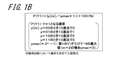
- 1 shows an example of an embodiment of a display data generation device of the present disclosure, and is an arithmetic expression that determines a probability in a probability circuit.
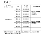
- 13 is a table illustrating another example of the display data generation device according to the present disclosure, and is a table illustrating that the dithering process is performed once every four frames.
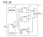
- It is a block circuit diagram of the stochastic circuit shown in FIG. 1A. It is a table explaining that the probability is variable by a plurality of lookup tables included in the probability circuit of FIG. 1A.
- the number of bits m of the first dithering data is 2
- the value ym in the decimal system is 0 to 3
- the maximum value ymax in the decimal system is 3, four lookups included in the probability circuit of FIG. 3A. It is a table explaining operation of one of the tables.
- FIG. 3 is a block circuit diagram of a basic configuration of an LCD having a configuration based on the liquid crystal display device of the present disclosure.
- the display data generation device and the display device of the present disclosure may include well-known constituent members such as a circuit board, wiring conductors, control IC, and LSI, which are not shown.
- FIG. 6 shows an example of the basic configuration of an active matrix type liquid crystal display device (Liquid Crystal Display: LCD) based on the liquid crystal display device of the present disclosure.
- the TFT array side substrate 20 on which a large number of pixel electrode portions P11, P12, P13 to Pmn including the TFT 21 are formed is arranged in the first direction (for example, the row).
- the first direction for example, the row.
- the gate signal lines GL1, GL2, GL3 to GLm and gate signal lines GL1, GL2, GL3 to GLm in a second direction (eg, column direction) intersecting the first direction.
- a common electrode for forming a lateral electric field (horizontal electric field) applied to the liquid crystal between the TFT 21, the pixel electrodes PE11, PE12, PE13 to PEmn and the pixel electrodes PE11, PE12, PE13 to PEmn.
- the configuration includes a pixel electrode portion and a common voltage line 22 that supplies a common voltage (Vcom) to the common electrode.
- Vcom common voltage
- This IPS type LCD can enhance viewing angle characteristics such as contrast, gray inversion, and color shift compared to an LCD that drives a Twisted Nematic (TN) liquid crystal by a vertical electric field. As a result, a wide viewing angle can be obtained, which is suitable for large-sized LCDs.
- TN Twisted Nematic
- the dithering method is a method that allows an image to be displayed with an apparently larger number of colors than the actual number of colors (the number of gradations).
- the dithering method is used, for example, when a single pixel portion is conspicuous more than necessary in a specific color tone, the periphery of the pixel portion is averaged as an intermediate color, and it is possible to suppress the conspicuousness more than necessary.
- the dithering method eliminates the boundary between the image areas. As a result, a natural gradation appears between the image areas, and color unevenness is eliminated.
- the display data generation device includes display data including dithering data in each unit pixel unit of a display device having a plurality of unit pixel units and driven by an active matrix method.
- a display data generating device for generating and supplying a binary high-order bit data consisting of a plurality of bits (n bits/n is an integer of 2 or more) and 2 consisting of 1 bit or more (m bits/m is a natural number).
- the first display data generation unit 1 that generates the first display data Din[n+m] having the binarized lower bit data and the binarized upper bit data as the second display data x are binarized.
- the probability circuit 4 having a probability varying unit and the third display data Dout[n] generated by adding the second dithering data Y[1] to the second display data x[n] are displayed on the display device 6 And a second display data generating unit 5 for supplying In the configuration of FIG.
- reference numeral 2 indicates a dithering portion
- reference numeral 3a indicates a storage portion of the second display data x in the data separating portion 3
- the second display data generation unit 5 is composed of an adder and the like.
- the probability circuit 4 that determines the second dithering data Y[n] to “1” or “0” with a probability has a probability varying unit, it is high in performing dithering of various images. Image quality becomes easy and the degree of freedom is improved. That is, it becomes easy to improve the image quality of various images. Further, since the third display data as the driving display data used for image display in each unit pixel portion of the display device can be generated and directly supplied to the display device, the display data such as the display memory is temporarily stored. No need for large memory. As a result, the display data transferred to the display device can be transferred at a high speed, the power consumption can be reduced, and the display device can be manufactured at low cost.
- the probability varying unit corresponds to a part including the selector 10, the lookup table (LUT) (0) 12, and the LUT (1) 13 to LUT (ymax) 14 shown in FIG. 3A.
- the display data generation device of the present embodiment basically relates to dithering processing executed in a unit pixel unit. Therefore, it is not related to the dithering process performed by referring to the display data of the unit pixel portion around the certain unit pixel portion.
- the display data of the peripheral unit pixel portion is intermittently and periodically added to the first display data Din[n+m]. By including it, it is possible to execute the dithering process with reference to the display data of the peripheral unit pixel portion.
- the display data generation device of the present embodiment may be a driving element such as an IC or LSI in which the dithering processing program is stored in ROM (Read Only Memory), RAM (Random Access Memory), etc. It may be a drive circuit device in which a peripheral circuit and electronic elements are mounted on a substrate. Further, the driving element and the driving circuit device may be arranged inside the display device, but may be arranged as an external component outside the display device.
- the binarized high-order bit data is about 2 to 12 bits. If it exceeds 12 bits, various circuits such as the drive circuit of the display device 6 tend to be complicated and the circuit scale tends to increase.
- the binarized lower bit data is, for example, about 1 bit to 4 bits. When the number of bits exceeds 4 bits, the dithering unit 2 becomes complicated and the small-capacity memory size such as LUT in the probability circuit 4 tends to increase.
- FIG. 1B is an arithmetic expression for determining the probability in the probability circuit 4.
- the stochastic circuit 4 of the present embodiment operates as follows.
- the probability circuit 4 sets the number of bits of the first dithering data y[m] to m (m is a natural number), the decimal value of the first dithering data y[m] to ym, and the first dithering.
- ymax is the maximum value of the data y[m] in the decimal system
- the second dithering data Y[1] is determined to be “1” with a probability of ⁇ ym/(ymax+1) ⁇ 100(%). ..
- the probability can be made variable by variously setting the bit number m of the first dithering data y[m], the decimal value ym, and the decimal maximum value ymax. Further, the maximum probability is ⁇ ymax/(ymax+1) ⁇ 100(%), which is not 100(%). Therefore, a small memory of a lookup table (LUT) corresponding to 100(%) can be omitted. , It can be disabled at all times. As a result, the number of small-capacity memories such as a look-up table (LUT) used in the probability circuit 4 can be suppressed, and power consumption can be suppressed.
- LUT lookup table
- FIG. 2 shows another example of the display data generation device according to the present embodiment, and is a table for explaining that the dithering process is performed once every four frames.
- the probability circuit 4 of the display data generating apparatus according to the present embodiment outputs the second dithering data Y[1] in ym frames of the selected (ymax+1) frames. It is better to decide "1". In this case, since the dithering process can be performed on the selected frame, the degree of freedom in improving the image quality of various images is improved.
- the second dithering data Y[1] is determined to be "1".
- the dithering data Y[1] of 2 is determined to be "1”.
- the dithering data Y[1] of 2 is determined to be "1".
- the dithering data Y[1] of 2 is determined to be "1".
- FIG. 2 shows a case where the first display data Din[8+2] has binarized high-order bit data of 8 bits and binarized low-order bit data of 2 bits.
- the binarized high-order bit data is data corresponding to the third display data Dout[n] for driving the display device.
- the binarized lower-order bit data corresponds to the second dithering data Y[1], and is added to the second display data x[n] to be finally reduced.
- the dithering process is executed in the third frame of the first to fourth frames. Further, the dithering process of adding “1” is executed in the fifth frame of the fifth to eighth frames.
- (ymax+1) frames may be consecutive (ymax+1) frames.
- all the frames can be the target of the dithering process, the image quality can be improved more effectively.
- the display data generation device includes a random number generation circuit 11 in the probability circuit 4, and the random number generation circuit 11 is the second of the (ymax+1) frames. It is preferable to select the frame that determines the dithering data Y[1] of “1”. In this case, it is possible to effectively suppress the occurrence of unnatural gradation and color unevenness in the display image. Further, the random number generation circuit 11 can also select a frame in which the second dithering data Y[1] is determined to be “1” from among the (ymax+1) frames with variable probability.
- any one of the output signals OUT1 and OUT2 to OUTymax+1 is input to one of the enable EN terminals of the LUT(0) and LUT(1) to LUT(ymax), and LUT(0) and LUT(1) to Any one of the LUTs (ymax) is activated (started) and operated.
- the output signal OUT1 is input to the enable terminal EN of the LUT(0) and activates the LUT(0).
- the output signal OUT2 is input to the enable terminal EN of the LUT(1) and activates the LUT(1).
- the output signal OUTymax+1 is input to the enable terminal EN of the LUT(ymax) and activates the LUT(ymax).
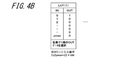
- a random selection signal is input from the random number generation circuit 11 to each of the input terminals IN of the LUT(0) and LUT(1) to LUT(ymax) together with any one of the output signals OUT1 and OUT2 to OUTymax+1 output from the selector 10. .. As shown in FIGS. 4A, 4B, and 4C, the random selection signal causes one of the LUT(0) and LUT(1) to LUT(ymax) to be activated and select one OUT data. ..
- the OUT data of the LUT(0) is all “0” as shown in FIG. 4A, so the OUT data is always “0”. That is, the LUT(0) has a probability of ⁇ 0/(ymax+1) ⁇ 100(%) as shown in the column of LUT(0) in FIG. 3B, and the second dithering data Y[1] is “ 1”.
- the LUT(1) When the LUT(1) is activated, as shown in FIG. 4B, only one OUT data of the LUT(1) is “1” and the rest is “0”, so the OUT data is ⁇ 1/( ymax+1) ⁇ 100(%) with a probability of “1”. That is, the LUT(1) has a probability of ⁇ 1/(ymax+1) ⁇ 100(%) as shown in the column of LUT(1) in FIG. 3B, and the second dithering data Y[1] is “ 1”.
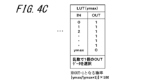
- the LUT(ymax) When the LUT(ymax) is activated, as shown in FIG. 4C, only one OUT data of the LUT(ymax) is “0” and the rest is “1”, so the OUT data is ⁇ ymax/( ymax+1) ⁇ 100(%) with a probability of “1”. That is, as shown in the LUT(ymax) column of FIG. 3B, the LUT(ymax) has the probability of ⁇ ymax/(ymax+1) ⁇ 100(%) and the second dithering data Y[1] is “ 1”.
- any one of the activated LUT(0) and LUT(1) to LUT(ymax) sets the second dithering data Y[1] to “1” with its unique probability. decide. In other words, in order to change the probability, any one of LUT(0) and LUT(1) to LUT(ymax) may be activated.
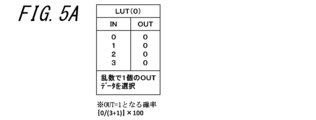
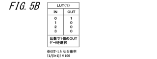
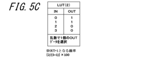
- 5A, 5B, 5C and 5D show that the bit number m of the first dithering data y[m] is 2, the decimal value ym is 0 to 3, and the decimal maximum value ymax is 3.
- 3B is a table for explaining the operation of each of the four LUT(0) to LUT(3) included in the probability circuit of FIG. 3A.
- the LUT(0) operates to determine the second dithering data Y[1] to be “1” with a probability of ⁇ 0/(3+1) ⁇ 100(%).
- the LUT(1) operates to determine the second dithering data Y[1] to be “1” with a probability of ⁇ 1/(3+1) ⁇ 100(%).
- the LUT(2) operates to determine the second dithering data Y[1] to be “1” with a probability of ⁇ 2/(3+1) ⁇ 100(%).
- the LUT(3) operates to determine the second dithering data Y[1] to be “1” with a probability of ⁇ 3/(3+1) ⁇ 100(%).
- the dithering data Y[1] of 2 can be determined to be "1". That is, the probability of determining the second dithering data Y[1] as “1” can be made variable to any of 0(%), 25(%), 50(%), and 75(%). it can.
- the display device of the present embodiment is a display device including the display data generation device of the present embodiment, and selects whether to take in the third display data Dout[n] generated by the display data generation device. It is the structure provided with the selection part. With this configuration, it is possible to select whether or not to execute the dithering process, and the degree of freedom of image processing for various images is further improved.
- the selection unit can be inserted and arranged in series in the transmission line between the third display data generation unit 5 and the display device 6, for example. It is possible to capture the third display data Dout[n] by setting the selection unit as a switch circuit and closing the switch circuit (ON state).
- the third display data Dout[n] can be prevented from being taken in. Further, when the third display data Dout[n] is not captured, the display data that has not been subjected to the dithering process may be input to the display device 6. Further, the third display data Dout[n] can be always taken in by setting the switch circuit to the normally closed state (on state).
- the display device of the present disclosure may be a display device having a plurality of unit pixel portions and driven by an active matrix method, and may be, for example, an LCD, an organic EL (Electro Luminescence) device, an inorganic EL device, a plasma display, an FED (Field). Emitting Display), SED (Surface-conduction Electron-emitter Display), GLV (Grating Light Valve) device, PDP (Plasma Display) device, DMD (Digital micro Mirror Device), piezoelectric ceramic display, micro LED display, etc. It may be.
- display data generation device and the display device of the present disclosure are not limited to the above-mentioned embodiment, and may include appropriate design changes and improvements.
- the present disclosure can have the following embodiments.
- a display data generation device of the present disclosure generates a display data including dithering data and supplies the display data including the dithering data to each of the unit pixel units of a display device having a plurality of unit pixel units and driven by an active matrix method.
- a first display data generation unit for generating first display data having binarized high-order bit data composed of a plurality of bits and binarized low-order bit data composed of 1 bit or more;
- a data separating unit that separates the binarized upper bit data into second display data and the binarized lower bit data as first dithering data, and a second dither that adds the binarized lower bit data to the second display data.
- the ring data is determined to be “1” with a probability based on the number of bits and the value of the first dithering data, and is determined to be “0” in other cases, and a probability variable unit that makes the probability variable is provided.
- a second display data generation unit that supplies third display data generated by adding the second dithering data to the second display data to the display device.
- the probability circuit is configured such that the number of bits of the first dithering data is m (m is a natural number), the decimal value of the first dithering data is ym, and the first dithering data is ym.
- ymax is the maximum value of the dithering data of 1 in the decimal system
- the second dithering data may be determined to be "1" with a probability of ⁇ ym/(ymax+1) ⁇ 100(%).
- the probability circuit may determine the second dithering data to be “1” in ym frames of the selected (ymax+1) frames.
- the probability circuit includes a random number generation unit, and the random number generation unit sets the second dithering data to “1” in the (ymax+1) frames.
- the frame to be determined may be selected.
- the (ymax+1) frames may be continuous (ymax+1) frames.
- a display device is a display device including the display data generation device according to the present disclosure, and includes a selection unit that selects whether to capture the third display data generated by the display data generation device. It has a structure.
- a display data generation device of the present disclosure generates a display data including dithering data and supplies the display data including the dithering data to each of the unit pixel units of a display device having a plurality of unit pixel units and driven by an active matrix method.
- a first display data generation unit for generating first display data having binarized high-order bit data composed of a plurality of bits and binarized low-order bit data composed of 1 bit or more;
- a data separating unit that separates the binarized upper bit data into second display data and the binarized lower bit data as first dithering data, and a second dither that adds the binarized lower bit data to the second display data.
- the ring data is determined to be “1” with a probability based on the number of bits and the value of the first dithering data, and is determined to be “0” in other cases, and a probability variable unit that makes the probability variable is provided.
- a second display data generation unit that supplies third display data generated by adding the second dithering data to the second display data to the display device. Therefore, the following effects are achieved. Since the probability circuit that determines the second dithering data to “1” or “0” with probability has the probability varying unit, it is easy to improve the image quality when performing dithering of various images. The degree of freedom increases as That is, it becomes easy to improve the image quality of various images.
- the display data transferred to the display device can be transferred at a high speed, the power consumption can be reduced, and the display device can be manufactured at low cost.
- the probability circuit is configured such that the number of bits of the first dithering data is m (m is a natural number), the decimal value of the first dithering data is ym, and When ymax is the maximum value of the dithering data of 1 in the decimal system, when the second dithering data is determined to be “1” with a probability of ⁇ ym/(ymax+1) ⁇ 100(%),
- the probability can be made variable by variously setting the bit number m of the dithering data, the decimal value ym, and the decimal maximum value ymax. Further, the maximum probability is ⁇ ymax/(ymax+1) ⁇ 100(%), which is not 100(%). Therefore, the number of small-capacity memories such as a lookup table (LUT) used in the probability circuit is Can be suppressed.
- LUT lookup table
- the display data generation device is selected when the probability circuit determines the second dithering data to be “1” in ym frames of the selected (ymax+1) frames.
- the dithering process can be performed on the selected frame. As a result, the degree of freedom in improving the image quality by the dithering process is improved.
- the probability circuit includes a random number generation unit, and the random number generation unit sets the second dithering data to “1” in the (ymax+1) frames.
- the (ymax+1) frames are continuous (ymax+1) frames, all the frames can be the target of the dithering process. As a result, more effective image quality can be achieved.
- a display device is a display device including the display data generation device according to the present disclosure, and includes a selection unit that selects whether to capture the third display data generated by the display data generation device. It has a structure. With this configuration, it is possible to select whether or not to execute the dithering process, and the degree of freedom of image processing for various images is further improved.
- the display data generation device and display device of the present disclosure can be applied to various electronic devices.
- the electronic devices include car route guidance system (car navigation system), ship route guidance system, aircraft route guidance system, smartphone terminal, mobile phone, tablet terminal, personal digital assistant (PDA), video camera, digital still camera, electronic device.
- ATM automatic teller machines
- HMD head mounted image display devices
Landscapes
- Engineering & Computer Science (AREA)
- Physics & Mathematics (AREA)
- Computer Hardware Design (AREA)
- General Physics & Mathematics (AREA)
- Theoretical Computer Science (AREA)
- Chemical & Material Sciences (AREA)
- Crystallography & Structural Chemistry (AREA)
- Multimedia (AREA)
- Signal Processing (AREA)
- Control Of Indicators Other Than Cathode Ray Tubes (AREA)
- Liquid Crystal Display Device Control (AREA)
- Transforming Electric Information Into Light Information (AREA)
Abstract
表示データ生成装置は、2値化上位ビットデータ(nビット)と2値化下位ビットデータ(mビット)とを有する第1の表示データDin[n+m]を生成する第1の表示データ生成部(1)と、2値化上位ビットデータを第2の表示データxとし、2値化下位ビットデータを第1のディザリングデータy(=y[m])として分離するデータ分離部(3)と、第2の表示データx(=x[n])に加算する第2のディザリングデータY[1]を、第1のディザリングデータy[m]のビット数mおよび値に基づく可変の確率で「1」に決定する確率回路(4)と、第2の表示データx[n]に第2のディザリングデータY[1]を加算して生成した第3の表示データDout[n]を、表示装置(6)に供給する第2の表示データ生成部(5)と、を備える。
Description
本開示は、アクティブマトリックス方式で駆動される表示装置の単位画素部のそれぞれにディザリングデータを含む表示データを生成し供給する表示データ生成装置および表示装置に関する。
従来のアクティブマトリクス型の液晶表示装置(Liquid Crystal Display:LCD)の基本構成の1例が、例えば特許文献1に記載されている。
本開示の表示データ生成装置は、複数の単位画素部を有しアクティブマトリックス方式で駆動される表示装置の前記単位画素部のそれぞれに、ディザリングデータを含む表示データを生成し供給する表示データ生成装置であって、複数ビットから成る2値化上位ビットデータと、1ビット以上から成る2値化下位ビットデータと、を有する第1の表示データを、生成する第1の表示データ生成部と、前記2値化上位ビットデータを第2の表示データとし、前記2値化下位ビットデータを第1のディザリングデータとして分離するデータ分離部と、前記第2の表示データに加算する第2のディザリングデータを、前記第1のディザリングデータのビット数および値に基づく確率で「1」に決定し、それ以外の場合は「0」に決定するとともに、前記確率を可変とする確率可変部を有する確率回路と、前記第2の表示データに前記第2のディザリングデータを加算して生成した第3の表示データを、前記表示装置に供給する第2の表示データ生成部と、を備える構成である。
本開示の表示装置は、上記本開示の表示データ生成装置を備える表示装置であって、前記表示データ生成装置で生成した前記第3の表示データを取り込むか否かを選択する選択部を備えている構成である。
本開示の目的、特色、および利点は、下記の詳細な説明と図面とからより明確になるであろう。
本開示の表示データ生成装置について実施の形態の1例を示すものであり、表示データ生成装置のブロック回路図である。
本開示の表示データ生成装置について実施の形態の1例を示すものであり、確率回路において確率を決定する演算式である。
本開示の表示データ生成装置について実施の形態の他例を示すものであり、4フレームに1回の割合でディザリング処理を行うことを説明する表である。
図1Aに示す確率回路のブロック回路図である。
図1Aの確率回路に含まれる複数のルックアップテーブルによって確率が可変とされることを説明する表である。
図3Aの確率回路に含まれる複数のルックアップテーブルのうちの1つの動作を説明する表である。
図3Aの確率回路に含まれる複数のルックアップテーブルのうちの1つの動作を説明する表である。
図3Aの確率回路に含まれる複数のルックアップテーブルのうちの1つの動作を説明する表である。
第1のディザリングデータのビット数mが2、10進法による値ymが0~3、10進法による最大値ymaxが3である場合に、図3Aの確率回路に含まれる4つのルックアップテーブルのうちの1つの動作を説明する表である。
第1のディザリングデータのビット数mが2、10進法による値ymが0~3、10進法による最大値ymaxが3である場合に、図3Aの確率回路に含まれる4つのルックアップテーブルのうちの1つの動作を説明する表である。
第1のディザリングデータのビット数mが2、10進法による値ymが0~3、10進法による最大値ymaxが3である場合に、図3Aの確率回路に含まれる4つのルックアップテーブルのうちの1つの動作を説明する表である。
第1のディザリングデータのビット数mが2、10進法による値ymが0~3、10進法による最大値ymaxが3である場合に、図3Aの確率回路に含まれる4つのルックアップテーブルのうちの1つの動作を説明する表である。
本開示の液晶表示装置が基礎とする構成のLCDの基本構成のブロック回路図である。
以下、本開示の表示データ生成装置および表示装置の実施の形態について、図面を参照しながら説明する。但し、以下で参照する各図は、本実施の形態の表示データ生成装置および表示装置の主要な構成部材等を示している。従って、本実施の形態の表示データ生成装置および表示装置は、図に示されていない回路基板、配線導体、制御IC,LSI等の周知の構成部材を備えていてもよい。
まず、図6を参照して、本開示の液晶表示装置が基礎とする構成の液晶表示装置について説明する。
本開示の液晶表示装置が基礎とする構成のアクティブマトリクス型の液晶表示装置(Liquid Crystal Display:LCD)の基本構成の1例を図6に示す。例えばIPS(In-Plane Switching)方式のLCDの場合、TFT21を含む画素電極部P11,P12,P13~Pmnが多数形成されたTFTアレイ側基板20は、その上の第1の方向(例えば、行方向)に形成された複数本のゲート信号線GL1,GL2,GL3~GLmと、第1の方向と交差する第2の方向(例えば、列方向)にゲート信号線GL1,GL2,GL3~GLmと交差させて形成された複数本の画像信号線(ソース信号線)SL1,SL2,SL3~SLnと、ゲート信号線GL1,GL2,GL3~GLmと画像信号線SL1,SL2,SL3~SLnの交差部に形成された、TFT21、画素電極PE11,PE12,PE13~PEmn及びその画素電極PE11,PE12,PE13~PEmnとの間で液晶に印加する横電界(水平電界)を形成するための共通電極を含む画素電極部と、共通電極に共通電圧(Vcom)を供給する共通電圧線22と、を有する構成である。なお、図6において、23はゲート信号線GL1,GL2,GL3~GLmに順次ゲート信号を入力するゲート信号線駆動回路、24は画像信号線SL1,SL2,SL3~SLnに順次画像信号を入力する画像信号線駆動回路である。このIPS方式のLCDは、垂直電界によってツイステッドネマチック(Twisted Nematic:TN)液晶を駆動するLCDと比較して、コントラスト、グレー反転、色ずれ等の視野角特性を高めることができる。その結果、広視野角を得ることができるので、大型のLCDに好適に用いられている。
また、このようなLCDは高解像度化、多諧調化が進んでおり、それらに対応して画質を向上させるために、疑似的に階調数を増やすディザリング法が用いられている。ディザリング法は、実際の色数(階調数)よりも見かけ上多くの色数で画像を表示できるようにする方法である。ディザリング法を用いると、例えば、単一の画素部が特定の色調で必要以上に目立つ場合、その画素部の周辺を中間色として平均化し、必要以上に目立つことを抑えることができる。また、複数の画素部から成る或る画像領域と、その周辺の画像領域との間の色調差が大きいために、画像領域間に境界線が見えるような不自然なグラデーション、色ムラが生じている場合、ディザリング法を用いると、画像領域間の境界線が解消される。その結果、画像領域間が自然なグラデーションに見え、色ムラも解消される。
本実施の形態の表示データ生成装置は、図1Aに示すように、複数の単位画素部を有しアクティブマトリックス方式で駆動される表示装置の単位画素部のそれぞれに、ディザリングデータを含む表示データを生成し供給する表示データ生成装置であって、複数ビット(nビット/nは2以上の整数)から成る2値化上位ビットデータと、1ビット以上(mビット/mは自然数)から成る2値化下位ビットデータと、を有する第1の表示データDin[n+m]を、生成する第1の表示データ生成部1と、2値化上位ビットデータを第2の表示データxとし、2値化下位ビットデータを第1のディザリングデータy(=y[m])として分離するデータ分離部3と、第2の表示データx(=x[n])に加算する第2のディザリングデータY[1]を、第1のディザリングデータy[m]のビット数mおよび値に基づく確率で「1」に決定し、それ以外の場合は「0」に決定するとともに、確率を可変とする確率可変部を有する確率回路4と、第2の表示データx[n]に第2のディザリングデータY[1]を加算して生成した第3の表示データDout[n]を、表示装置6に供給する第2の表示データ生成部5と、備える構成である。なお、図1Aの構成において、符号2はディザリング部を示し、符号3aはデータ分離部3における第2の表示データxの格納部を示し、符号3bは第1のディザリングデータy(=y[m])の格納部を示す。また、第2の表示データ生成部5は加算器等から成る。
上記の構成により、以下の効果を奏する。第2のディザリングデータY[n]を確率をもって「1」または「0」に決定する確率回路4が、確率可変部を有していることから、種々の画像のディザリングを実施するにあたって高画質化が容易になるとともにその自由度が向上する。すなわち、種々の画像の画質を向上させることが容易になる。また、表示装置の各単位画素部で画像表示に用いられる駆動用の表示データとしての第3の表示データを生成し表示装置に直接的に供給できるので、表示メモリ等の表示データを一旦記憶する大容量のメモリが不要となる。その結果、表示装置に転送する表示データの転送速度が速くなるとともに、消費電力が低減され、さらには低コストな表示装置となる、という効果も奏する。なお、確率可変部は、図3Aに示すセレクタ10、ルックアップテーブル(LUT)(0)12、LUT(1)13~LUT(ymax)14から構成される部位に相当する。
なお、本実施の形態の表示データ生成装置は、基本的には或る単位画素部において実行されるディザリング処理に関するものである。従って、或る単位画素部の周辺の単位画素部の表示データを参照して行うディザリング処理に関するものではない。しかしながら、第1の表示データDin[n+m]を生成する第1の表示データ生成部1において、第1の表示データDin[n+m]に、周辺の単位画素部の表示データを断続的、周期的に含ませることによって、周辺の単位画素部の表示データを参照してディザリング処理を実行させることも可能である。
本実施の形態の表示データ生成装置は、ディザリング処理プログラムがROM(Read Only Memory),RAM(Random Access Memory)等に格納されたIC,LSI等の駆動素子であってよく、またその駆動素子と周辺回路および電子素子を基板上に搭載した駆動回路装置であってもよい。また、駆動素子、駆動回路装置は、表示装置の内部に配置されていてもよいが、表示装置の外部に外付けの部品として配置されていてもよい。
nビット(nは2以上の整数)から成る2値化上位ビットデータと、mビット(mは自然数)から成る2値化下位ビットデータと、を有する第1の表示データDin[n+m]において、例えば2値化上位ビットデータは2ビット~12ビット程度である。12ビットを超えると、表示装置6の駆動回路等の各種回路が複雑化し、回路規模が大きくなる傾向がある。2値化下位ビットデータは、例えば1ビット~4ビット程度である。4ビットを超えると、ディザリング部2が複雑化するとともに確率回路4におけるLUT等の小容量のメモリサイズが大きくなっていく傾向がある。
図1Bは確率回路4において確率を決定する演算式である。この演算式に基づき、本実施の形態の確率回路4は以下のように動作する。確率回路4は、第1のディザリングデータy[m]のビット数をm(mは自然数)、第1のディザリングデータy[m]の10進法による値をym、第1のディザリングデータy[m]の10進法による最大値をymaxとしたとき、{ym/(ymax+1)}×100(%)の確率で第2のディザリングデータY[1]を「1」に決定する。
図1Bの演算式によると、例えば第1のディザリングデータy[m]のビット数mが2である場合、第1のディザリングデータy[m]が「00」の場合に10進法で「0」、y[m]が「01」の場合に10進法で「1」、y[m]が「10」の場合に10進法で「2」、y[m]が「11」の場合に10進法で「3」であることから、第2のディザリングデータY[1]が「1」となる確率P(Y1)は、0%,1/4(25%),2/4(50%),3/4(75%)のいずれかの確率となる。
従って、第1のディザリングデータy[m]のビット数mと10進法による値ymと10進法による最大値ymaxとを種々に設定することによって、確率を可変にすることができる。また、確率は最大でも{ymax/(ymax+1)}×100(%)となり、100(%)にはならないので、100(%)に相当するルックアップテーブル(LUT)の小容量のメモリを省いたり、常時動作させないようにすることができる。その結果、確率回路4の中に用いるルックアップテーブル(LUT)等の小容量のメモリの数を抑えたり、消費電力を抑えることができる。
図2は、本実施の形態の表示データ生成装置について実施の形態の他例を示すものであり、4フレームに1回の割合でディザリング処理を行うことを説明する表である。図2に示すように、本実施の形態の表示データ生成装置の確率回路4は、選択された(ymax+1)個のフレームのうちym個のフレームにおいて、第2のディザリングデータY[1]を「1」に決定することがよい。この場合、選択されたフレームにおいてディザリング処理を実施することができるので、種々の画像の高画質化に関してその自由度が向上する。なお、mが2でy[m]が「00」の場合には、10進法による値ymは0であるから、選択された(ymax+1)=4個のフレームのうちym=0個のフレームにおいて第2のディザリングデータY[1]を「1」に決定する。mが2でy[m]が「01」の場合には、10進法による値ymは1であるから、選択された(ymax+1)=4個のフレームのうちym=1個のフレームにおいて第2のディザリングデータY[1]を「1」に決定する。mが2でy[m]が「10」の場合には、10進法による値ymは2であるから、選択された(ymax+1)=4個のフレームのうちym=2個のフレームにおいて第2のディザリングデータY[1]を「1」に決定する。mが2でy[m]が「11」の場合には、10進法による値ymは3であるから、選択された(ymax+1)=4個のフレームのうちym=3個のフレームにおいて第2のディザリングデータY[1]を「1」に決定する。図2に示す構成は、mが2でy[m]が「01」の場合であり、10進法による値ymは1であるから、選択された(ymax+1)=4個のフレームのうちym=1個のフレームにおいて第2のディザリングデータY[1]を「1」に決定する場合に相当する。
図2は、第1の表示データDin[8+2]が、8ビットから成る2値化上位ビットデータと、2ビットから成る2値化下位ビットデータと、を有する場合を示す。なお、2値化上位ビットデータは、表示装置の駆動用の第3の表示データDout[n]に相当するデータである。2値化下位ビットデータは、第2のディザリングデータY[1]に相当し、第2の表示データx[n]に加算されることによって、最終的には削減されることとなる。
図2の例においては、第1フレーム~第4フレームのうち、第3フレームにおいてディザリング処理が実行されている。また、第5フレーム~第8フレームのうち、第5フレームにおいて「1」を加算するディザリング処理が実行されている。
また本実施の形態の表示データ生成装置は、図2に示すように、(ymax+1)個のフレーム(例えば、4個のフレーム)は、連続した(ymax+1)個のフレームであることがよい。この場合、すべてのフレームをディザリング処理の対象とすることができるので、より効果的に高画質化ができる。
また本実施の形態の表示データ生成装置は、図3Aに示すように、確率回路4は、乱数発生回路11を備えており、乱数発生回路11は、(ymax+1)個のフレームのうち、第2のディザリングデータY[1]を「1」に決定するフレームを選択することがよい。この場合、表示画像において不自然なグラデーション、色ムラが発生することを効果的に抑えることができる。また乱数発生回路11は、(ymax+1)個のフレームのうち、第2のディザリングデータY[1]を「1」に決定するフレームを、確率を可変として選択することもできる。
図3Aの確率回路4において、セレクタ10は、第1のディザリングデータy[m]のビット数mと値(2進法による値)によって、OUT1,OUT2~OUTymax+1のいずれかの出力信号を選択する。mが2でy[m]が「00」の場合、出力信号OUT1が選択される。mが2でy[m]が「01」の場合、出力信号OUT2が選択される。mが2でy[m]が「11」(=ymax:10進法で3)の場合、出力信号OUTymax+1が選択される。
そして、出力信号OUT1,OUT2~OUTymax+1のいずれかは、LUT(0),LUT(1)~LUT(ymax)のいずれかのイネーブルEN端子に入力されて、LUT(0),LUT(1)~LUT(ymax)のいずれか1つを活性化(起動)し動作させる。出力信号OUT1はLUT(0)のイネーブル端子ENに入力されてLUT(0)を活性化する。出力信号OUT2はLUT(1)のイネーブル端子ENに入力されてLUT(1)を活性化する。出力信号OUTymax+1はLUT(ymax)のイネーブル端子ENに入力されてLUT(ymax)を活性化する。
セレクタ10からの出力信号OUT1,OUT2~OUTymax+1のいずれかの出力とともに、乱数発生回路11からLUT(0),LUT(1)~LUT(ymax)の各入力端子INに、ランダム選択信号を入力する。ランダム選択信号は、図4A、図4Bおよび図4Cに示すように、LUT(0),LUT(1)~LUT(ymax)のうちの活性化した1つにおいて、1個のOUTデータを選択させる。
例えば、LUT(0)が活性化している場合、図4Aに示すように、LUT(0)のOUTデータは全て「0」であるので、OUTデータは必ず「0」になる。すなわち、LUT(0)は、図3BのLUT(0)の欄に示すように、{0/(ymax+1)}×100(%)の確率で、第2のディザリングデータY[1]を「1」に決定する。
LUT(1)が活性化している場合、図4Bに示すように、LUT(1)のOUTデータは1個だけ「1」で残りは全て「0」であるので、OUTデータは{1/(ymax+1)}×100(%)の確率で「1」となる。すなわち、LUT(1)は、図3BのLUT(1)の欄に示すように、{1/(ymax+1)}×100(%)の確率で、第2のディザリングデータY[1]を「1」に決定する。
LUT(ymax)が活性化している場合、図4Cに示すように、LUT(ymax)のOUTデータは1個だけ「0」で残りは全て「1」であるので、OUTデータは{ymax/(ymax+1)}×100(%)の確率で「1」となる。すなわち、LUT(ymax)は、図3BのLUT(ymax)の欄に示すように、{ymax/(ymax+1)}×100(%)の確率で、第2のディザリングデータY[1]を「1」に決定する。
このように、LUT(0),LUT(1)~LUT(ymax)のうちの活性化したいずれか1つが、その固有の確率でもって第2のディザリングデータY[1]を「1」に決定する。換言すれば、確率を変動させるためには、LUT(0),LUT(1)~LUT(ymax)のうちいずれか1つを活性化させればよいこととなる。
図5A、図5B、図5Cおよび図5Dは、第1のディザリングデータy[m]のビット数mが2、10進法による値ymが0~3、10進法による最大値ymaxが3である場合に、図3Aの確率回路に含まれる4つのLUT(0)~LUT(3)のそれぞれの動作を説明する表である。LUT(0)は、{0/(3+1)}×100(%)の確率で、第2のディザリングデータY[1]を「1」に決定するように動作する。LUT(1)は、{1/(3+1)}×100(%)の確率で、第2のディザリングデータY[1]を「1」に決定するように動作する。LUT(2)は、{2/(3+1)}×100(%)の確率で、第2のディザリングデータY[1]を「1」に決定するように動作する。LUT(3)は、{3/(3+1)}×100(%)の確率で、第2のディザリングデータY[1]を「1」に決定するように動作する。このように、LUT(0)~LUT(3)のいずれかを活性化させることにより、0(%),25(%),50(%),75(%)のいずれかの確率で、第2のディザリングデータY[1]を「1」に決定することができる。すなわち、第2のディザリングデータY[1]を「1」に決定する確率を、0(%),25(%),50(%),75(%)のいずれかに可変とすることができる。
本実施の形態の表示装置は、上記本実施の形態の表示データ生成装置を備える表示装置であって、表示データ生成装置で生成した第3の表示データDout[n]を取り込むか否かを選択する選択部を備えている構成である。この構成により、ディザリング処理を実行するか否かの選択が可能となり、種々の画像に対する画像処理の自由度がさらに向上する。選択部は、図1Aの構成において、例えば第3の表示データ生成部5と表示装置6との間の伝送線に直列に挿入配置することができる。選択部をスイッチ回路とし、スイッチ回路を閉状態(オン状態)とすることによって第3の表示データDout[n]を取り込むようにすることができる。スイッチ回路を開状態(オフ状態)とすることによって第3の表示データDout[n]を取り込まないようにすることができる。また、第3の表示データDout[n]を取り込まない場合、ディザリング処理をしていない表示データを表示装置6に入力してもよい。また、スイッチ回路を常時閉状態(オン状態)とすることによって第3の表示データDout[n]を常時取り込むようにすることができる。
本開示の表示装置は、複数の単位画素部を有しアクティブマトリックス方式で駆動される表示装置であればよく、例えばLCD,有機EL(Electro Luminescence)装置、無機EL装置、プラズマディスプレイ、FED(Field Emitting Display)、SED(Surface-conduction Electron-emitter Display)、GLV(Grating Light Valve)装置、PDP(Plasma Display)装置、DMD(Digital micro Mirror Device)、圧電セラミックディスプレイ、マイクロLEDディスプレイなどの表示装置であってもよい。
なお、本開示の表示データ生成装置および表示装置は、上記実施の形態に限定されるものではなく、適宜の設計的な変更、改良を含んでいてもよい。
本開示は、次の実施の形態が可能である。
本開示の表示データ生成装置は、複数の単位画素部を有しアクティブマトリックス方式で駆動される表示装置の前記単位画素部のそれぞれに、ディザリングデータを含む表示データを生成し供給する表示データ生成装置であって、複数ビットから成る2値化上位ビットデータと、1ビット以上から成る2値化下位ビットデータと、を有する第1の表示データを、生成する第1の表示データ生成部と、前記2値化上位ビットデータを第2の表示データとし、前記2値化下位ビットデータを第1のディザリングデータとして分離するデータ分離部と、前記第2の表示データに加算する第2のディザリングデータを、前記第1のディザリングデータのビット数および値に基づく確率で「1」に決定し、それ以外の場合は「0」に決定するとともに、前記確率を可変とする確率可変部を有する確率回路と、前記第2の表示データに前記第2のディザリングデータを加算して生成した第3の表示データを、前記表示装置に供給する第2の表示データ生成部と、を備える構成である。
本発明の表示データ生成装置は、前記確率回路は、前記第1のディザリングデータのビット数をm(mは自然数)、前記第1のディザリングデータの10進法による値をym、前記第1のディザリングデータの10進法による最大値をymaxとしたとき、{ym/(ymax+1)}×100(%)の確率で第2のディザリングデータを「1」に決定してもよい。
また本開示の表示データ生成装置は、前記確率回路は、選択された(ymax+1)個のフレームのうちym個のフレームにおいて、前記第2のディザリングデータを「1」に決定してもよい。
また本開示の表示データ生成装置は、前記確率回路は、乱数発生部を備えており、前記乱数発生部は、前記(ymax+1)個のフレームのうち、前記第2のディザリングデータを「1」に決定するフレームを選択してもよい。
また本開示の表示データ生成装置は、前記(ymax+1)個のフレームは、連続した(ymax+1)個のフレームであってもよい。
本開示の表示装置は、上記本開示の表示データ生成装置を備える表示装置であって、前記表示データ生成装置で生成した前記第3の表示データを取り込むか否かを選択する選択部を備えている構成である。
本開示の表示データ生成装置は、複数の単位画素部を有しアクティブマトリックス方式で駆動される表示装置の前記単位画素部のそれぞれに、ディザリングデータを含む表示データを生成し供給する表示データ生成装置であって、複数ビットから成る2値化上位ビットデータと、1ビット以上から成る2値化下位ビットデータと、を有する第1の表示データを、生成する第1の表示データ生成部と、前記2値化上位ビットデータを第2の表示データとし、前記2値化下位ビットデータを第1のディザリングデータとして分離するデータ分離部と、前記第2の表示データに加算する第2のディザリングデータを、前記第1のディザリングデータのビット数および値に基づく確率で「1」に決定し、それ以外の場合は「0」に決定するとともに、前記確率を可変とする確率可変部を有する確率回路と、前記第2の表示データに前記第2のディザリングデータを加算して生成した第3の表示データを、前記表示装置に供給する第2の表示データ生成部と、を備える構成であることから、以下の効果を奏する。第2のディザリングデータを確率をもって「1」または「0」に決定する確率回路が、確率可変部を有していることから、種々の画像のディザリングを実施するにあたって、高画質化が容易になるとともにその自由度が向上する。すなわち、種々の画像の画質を向上させることが容易になる。また、表示装置の各画素部で画像表示に用いられる駆動用の表示データとしての第3の表示データを生成し表示装置に直接的に供給できるので、表示メモリ等の表示データを一旦記憶する大容量のメモリが不要となる。その結果、表示装置に転送する表示データの転送速度が速くなるとともに、消費電力が低減され、さらには低コストな表示装置となる、という効果も奏する。
本開示の表示データ生成装置は、前記確率回路は、前記第1のディザリングデータのビット数をm(mは自然数)、前記第1のディザリングデータの10進法による値をym、前記第1のディザリングデータの10進法による最大値をymaxとしたとき、{ym/(ymax+1)}×100(%)の確率で第2のディザリングデータを「1」に決定する場合、第1のディザリングデータのビット数mと10進法による値ymと10進法による最大値ymaxとを種々に設定することによって、確率を可変にすることができる。また、確率は最大でも{ymax/(ymax+1)}×100(%)となり、100(%)にはならないので、確率回路の中に用いるルックアップテーブル(LUT)等の小容量のメモリの数を抑えることができる。
また本開示の表示データ生成装置は、前記確率回路は、選択された(ymax+1)個のフレームのうちym個のフレームにおいて、前記第2のディザリングデータを「1」に決定する場合、選択されたフレームにおいてディザリング処理を実施することができる。その結果、ディザリング処理による高画質化の自由度が向上する。
また本開示の表示データ生成装置は、前記確率回路は、乱数発生部を備えており、前記乱数発生部は、前記(ymax+1)個のフレームのうち、前記第2のディザリングデータを「1」に決定するフレームを選択する場合、不自然なグラデーション、色ムラが発生することを効果的に抑えることができる。
また本開示の表示データ生成装置は、前記(ymax+1)個のフレームは、連続した(ymax+1)個のフレームである場合、すべてのフレームをディザリング処理の対象とすることができる。その結果、より効果的な高画質化ができる。
本開示の表示装置は、上記本開示の表示データ生成装置を備える表示装置であって、前記表示データ生成装置で生成した前記第3の表示データを取り込むか否かを選択する選択部を備えている構成である。この構成により、ディザリング処理を実行するか否かの選択が可能となり、種々の画像に対する画像処理の自由度がさらに向上する。
本開示の表示データ生成装置および表示装置は各種の電子機器に適用できる。その電子機器としては、自動車経路誘導システム(カーナビゲーションシステム)、船舶経路誘導システム、航空機経路誘導システム、スマートフォン端末、携帯電話、タブレット端末、パーソナルデジタルアシスタント(PDA)、ビデオカメラ、デジタルスチルカメラ、電子手帳、電子書籍、電子辞書、パーソナルコンピュータ、複写機、ゲーム機器の端末装置、テレビジョン、商品表示タグ、価格表示タグ、産業用のプログラマブル表示装置、カーオーディオ、デジタルオーディオプレイヤー、ファクシミリ、プリンター、現金自動預け入れ払い機(ATM)、自動販売機、ヘッドアップディスプレイ装置、プロジェクタ装置、デジタル表示式腕時計、スマートウォッチ、頭部装着型画像表示装置(Head Mounted Display device :HMD)などがある。
本開示は、その精神または主要な特徴から逸脱することなく、他のいろいろな形態で実施できる。したがって、前述の実施形態はあらゆる点で単なる例示に過ぎず、本開示の範囲は特許請求の範囲に示すものであって、明細書本文には何ら拘束されない。さらに、特許請求の範囲に属する変形や変更は全て本開示の範囲内のものである。
1 第1の表示データ生成部
2 ディザリング部
3 データ分離部
4 確率回路
5 第2の表示データ生成部
6 表示装置
2 ディザリング部
3 データ分離部
4 確率回路
5 第2の表示データ生成部
6 表示装置
Claims (6)
- 複数の単位画素部を有しアクティブマトリックス方式で駆動される表示装置の前記単位画素部のそれぞれに、ディザリングデータを含む表示データを生成し供給する表示データ生成装置であって、
複数ビットから成る2値化上位ビットデータと、1ビット以上から成る2値化下位ビットデータと、を有する第1の表示データを、生成する第1の表示データ生成部と、
前記2値化上位ビットデータを第2の表示データとし、前記2値化下位ビットデータを第1のディザリングデータとして分離するデータ分離部と、
前記第2の表示データに加算する第2のディザリングデータを、前記第1のディザリングデータのビット数および値に基づく確率で「1」に決定し、それ以外の場合は「0」に決定するとともに、前記確率を可変とする確率可変部を有する確率回路と、
前記第2の表示データに前記第2のディザリングデータを加算して生成した第3の表示データを、前記表示装置に供給する第2の表示データ生成部と、を備える表示データ生成装置。 - 前記確率回路は、前記第1のディザリングデータのビット数をm(mは自然数)、前記第1のディザリングデータの10進法による値をym、前記第1のディザリングデータの10進法による最大値をymaxとしたとき、{ym/(ymax+1)}×100(%)の確率で第2のディザリングデータを「1」に決定する請求項1に記載の表示データ生成装置。
- 前記確率回路は、選択された(ymax+1)個のフレームのうちym個のフレームにおいて、前記第2のディザリングデータを「1」に決定する請求項2に記載の表示データ生成装置。
- 前記確率回路は、乱数発生部を備えており、
前記乱数発生部は、前記(ymax+1)個のフレームのうち、前記第2のディザリングデータを「1」に決定するフレームを選択する請求項3に記載の表示データ生成装置。 - 前記(ymax+1)個のフレームは、連続した(ymax+1)個のフレームである請求項3または4に記載の表示データ生成装置。
- 請求項1~5のいずれか1項に記載の表示データ生成装置を備える表示装置であって、
前記表示データ生成装置で生成した前記第3の表示データを取り込むか否かを選択する選択部を備えている表示装置。
Applications Claiming Priority (2)
| Application Number | Priority Date | Filing Date | Title |
|---|---|---|---|
| JP2019018079A JP2022046836A (ja) | 2019-02-04 | 2019-02-04 | 表示データ生成装置および表示装置 |
| JP2019-018079 | 2019-02-04 |
Publications (1)
| Publication Number | Publication Date |
|---|---|
| WO2020162017A1 true WO2020162017A1 (ja) | 2020-08-13 |
Family
ID=71948201
Family Applications (1)
| Application Number | Title | Priority Date | Filing Date |
|---|---|---|---|
| PCT/JP2019/047392 Ceased WO2020162017A1 (ja) | 2019-02-04 | 2019-12-04 | 表示データ生成装置および表示装置 |
Country Status (2)
| Country | Link |
|---|---|
| JP (1) | JP2022046836A (ja) |
| WO (1) | WO2020162017A1 (ja) |
Citations (2)
| Publication number | Priority date | Publication date | Assignee | Title |
|---|---|---|---|---|
| US20150279319A1 (en) * | 2014-03-26 | 2015-10-01 | Ati Technologies Ulc | Spatial dithering for a display panel |
| WO2018104993A1 (ja) * | 2016-12-05 | 2018-06-14 | Eizo株式会社 | 情報処理装置及びプログラム |
-
2019
- 2019-02-04 JP JP2019018079A patent/JP2022046836A/ja active Pending
- 2019-12-04 WO PCT/JP2019/047392 patent/WO2020162017A1/ja not_active Ceased
Patent Citations (2)
| Publication number | Priority date | Publication date | Assignee | Title |
|---|---|---|---|---|
| US20150279319A1 (en) * | 2014-03-26 | 2015-10-01 | Ati Technologies Ulc | Spatial dithering for a display panel |
| WO2018104993A1 (ja) * | 2016-12-05 | 2018-06-14 | Eizo株式会社 | 情報処理装置及びプログラム |
Also Published As
| Publication number | Publication date |
|---|---|
| JP2022046836A (ja) | 2022-03-24 |
Similar Documents
| Publication | Publication Date | Title |
|---|---|---|
| US7304624B2 (en) | Liquid crystal display apparatus and method for driving the same | |
| KR102255299B1 (ko) | 타이밍 컨트롤러, 표시장치 및 구동방법 | |
| JP4980508B2 (ja) | 液晶表示装置、モノクローム液晶表示装置、コントローラ、および画像変換方法 | |
| US8253677B2 (en) | Display device and method of driving the same | |
| US20070024557A1 (en) | Video signal processor, display device, and method of driving the same | |
| US20140247289A1 (en) | Display device and processing method of image signal | |
| CN107342034B (zh) | 显示面板驱动器、显示设备以及显示面板的驱动方法 | |
| KR20190073637A (ko) | 저계조 단색 영상 보상을 수행하는 표시 장치, 및 표시 장치의 구동 방법 | |
| JP6111588B2 (ja) | 液晶表示装置及びその駆動方法 | |
| US11132978B2 (en) | Gamma correction circuit, method for gamma correction, and display device including gamma correction circuit | |
| CN109326252B (zh) | 显示驱动器、显示控制器、电光装置和电子设备 | |
| KR101197055B1 (ko) | 표시 장치의 구동 장치 | |
| US10192509B2 (en) | Display apparatus and a method of operating the same | |
| CN101772800B (zh) | 液晶显示装置及其驱动方法、以及驱动电路 | |
| WO2018061917A1 (ja) | 表示装置 | |
| JP2018072653A (ja) | 電気光学装置、電子機器および駆動方法 | |
| WO2020162017A1 (ja) | 表示データ生成装置および表示装置 | |
| KR100848093B1 (ko) | 액정 표시 장치의 디더링 장치 및 디더링 방법 | |
| CN114512083A (zh) | 显示装置 | |
| KR102552303B1 (ko) | 표시 장치 및 그의 구동 방법 | |
| KR102509878B1 (ko) | 시간분할 구동 방법 및 이를 구현하는 장치 | |
| CN114974124A (zh) | 显示驱动电路、显示装置和显示驱动电路的操作方法 | |
| KR101217512B1 (ko) | 액정표시장치의 구동회로 및 이의 구동방법 | |
| JP2011137929A (ja) | 電気光学装置の駆動方法、電気光学装置の駆動装置、電気光学装置及び電子機器 | |
| JP2010085920A (ja) | 表示装置 |
Legal Events
| Date | Code | Title | Description |
|---|---|---|---|
| 121 | Ep: the epo has been informed by wipo that ep was designated in this application |
Ref document number: 19914450 Country of ref document: EP Kind code of ref document: A1 |
|
| NENP | Non-entry into the national phase |
Ref country code: DE |
|
| 122 | Ep: pct application non-entry in european phase |
Ref document number: 19914450 Country of ref document: EP Kind code of ref document: A1 |
|
| NENP | Non-entry into the national phase |
Ref country code: JP |