WO2020158944A1 - 電子部品搭載用パッケージ、電子装置及び電子部品搭載用パッケージの基体 - Google Patents
電子部品搭載用パッケージ、電子装置及び電子部品搭載用パッケージの基体 Download PDFInfo
- Publication number
- WO2020158944A1 WO2020158944A1 PCT/JP2020/003788 JP2020003788W WO2020158944A1 WO 2020158944 A1 WO2020158944 A1 WO 2020158944A1 JP 2020003788 W JP2020003788 W JP 2020003788W WO 2020158944 A1 WO2020158944 A1 WO 2020158944A1
- Authority
- WO
- WIPO (PCT)
- Prior art keywords
- electronic component
- component mounting
- bonding material
- protrusion
- mounting package
- Prior art date
- Legal status (The legal status is an assumption and is not a legal conclusion. Google has not performed a legal analysis and makes no representation as to the accuracy of the status listed.)
- Ceased
Links
Images



Classifications
-
- H—ELECTRICITY
- H10—SEMICONDUCTOR DEVICES; ELECTRIC SOLID-STATE DEVICES NOT OTHERWISE PROVIDED FOR
- H10W—GENERIC PACKAGES, INTERCONNECTIONS, CONNECTORS OR OTHER CONSTRUCTIONAL DETAILS OF DEVICES COVERED BY CLASS H10
- H10W70/00—Package substrates; Interposers; Redistribution layers [RDL]
- H10W70/60—Insulating or insulated package substrates; Interposers; Redistribution layers
Definitions
- the present disclosure relates to an electronic component mounting package, an electronic device, and a base of an electronic component mounting package.
- an electronic component mounting package that has a wiring board having a wiring pattern that is joined to an electronic component and a base body that is joined to the wiring substrate.
- the base has a base and a protrusion having a protrusion shape protruding in a direction perpendicular to the base, and the wiring substrate has a protrusion of the base. Located on the department. As a result, the positional relationship between the electronic component located on the wiring board and the base body becomes clear.
- a base having a first surface and a protrusion having a second surface protruding from the first surface and in contact with the first surface,
- the second surface includes a portion whose angle with respect to the first surface is less than 90 degrees. It is a package for mounting electronic components.
- a base having a first surface, A protrusion having a second surface protruding from the first surface and in contact with the first surface; Including The second surface includes a portion whose angle with respect to the first surface is less than 90 degrees. It is the base of a package for mounting electronic components.
- FIG. 3 is a cross-sectional view of the electronic component mounting package of the present embodiment on a plane including the signal line and perpendicular to the first plane. It is sectional drawing of the modification 1 of the package for electronic component mounting. It is sectional drawing of the modification 2 of an electronic component mounting package. It is sectional drawing of the modification 3 of the package for electronic component mounting. It is sectional drawing of the modification 4 of the package for electronic component mounting.
- FIG. 1 is an overall perspective view of the electronic device 1 of this embodiment.
- the electronic device 1 includes an electronic component mounting package 100 and an electronic component 200.
- the electronic component mounting package 100 includes a base 11, a signal line 12, a wiring board 14, a bonding material 15, a conductive bonding material 16, and the like.
- the base 11 is a conductive metal and functions as a ground plane.
- the substrate 11 one having a high thermal conductivity may be used. That is, the base 11 has a function as a heat sink that prevents the electronic component 200 from overheating due to heat being transferred from the electronic component 200 to the base 11.
- the base 11 has a base 111 and a protrusion 112.
- the base 111 may have a disc shape having a diameter of 3 to 10 mm and a thickness of 0.5 to 2.0 mm, for example, but is not limited thereto.
- the base 111 has a through hole 111a. The inside of the through hole 111a is occupied by the insulating member 113.
- the insulating member 113 may be, for example, a glass or ceramic material. The material of the insulating member 113 and the size of the through hole 111a may be determined according to desired characteristic impedance related to signal transmission by the signal line 12.
- the base 111 and the protrusion 112 may be integrated.
- the protrusion 112 projects from the first surface 111b of the base 111 including one end of the through hole 111a.
- the protrusion 112 has a second surface 112a that is in contact with the first surface 111b.
- the wiring substrate 14 is positioned on the surface of the second surface 112 a, that is, on the upper surface 1121 of the protrusion 112 in FIG. 1 via the bonding material 15.
- the protrusion 112 has a so-called semi-cylindrical shape in which a cylinder having an axis in the extending direction (X direction) of the signal line 12 described later is halved.
- the wiring board 14 includes a third surface 14a, a fourth surface 14b, and a fifth surface 14c, as shown in FIG.
- the third surface 14a has a wiring pattern 141.
- the fourth surface 14b is on the opposite side of the third surface 14a and has a ground pattern 142.
- the fifth surface 14c is in contact with the third surface 14a and the fourth surface 14b and faces the first surface 111b.
- the fifth surface 14c is also in contact with the first surface 111b.
- the wiring board 14 may be used, for example, as a high-frequency line board.
- the wiring board 14 is a flat insulating plate and may be made of resin, for example.
- the third surface 14a may be located on the side opposite to the second surface 112a and parallel to the fourth surface 14b.
- the thickness and material of the wiring board 14, particularly the relative permittivity may be appropriately determined according to desired characteristic impedance related to signal transmission by the wiring pattern 141.
- the wiring pattern 141 is located on the third surface 14a, electrically connected to the electronic component 200, and supplies electric power and a signal to the electronic component 200.
- the wiring pattern 141 may be a conductive metal film having a low resistance, here, a gold (Au) thin film.
- the wiring pattern 141 is bonded to the signal line 12 at two locations via the conductive bonding material 16.
- the shape, length, and position of the wiring pattern may be appropriately determined according to the size and terminal position of the electronic component 200 to be connected.
- the wiring pattern 141 is separated from the bonding material 15 by the wiring board 14. That is, on the wiring board 14, a signal is transmitted by the microstrip line.
- the ground pattern 142 is located on the fourth surface 14b and forms a ground surface for the wiring pattern 141.
- the ground pattern 142 may have various shapes according to the shape of the wiring pattern 141.
- the ground pattern 142 may be a solid electrode arranged so as to surround the area where the wiring pattern 141 is located when viewed from above the wiring pattern 141.
- the ground pattern 142 is, for example, a gold (Au) thin film.
- the bonding material 15 is a material whose thickness can be appropriately adjusted when bonding the wiring boards 14. Examples of such a material include those having an appropriate viscosity, for example, those having a viscosity of 30 to 250 [Pa ⁇ s ⁇ 1 ]. If the viscosity is lower than this, the bonding material 15 flows during bonding and it becomes difficult to maintain an appropriate shape. On the contrary, if the viscosity is too high, it becomes difficult to adjust the shape of the bonding material 15. Further, the bonding material 15 is bonded not only to the protrusion 112 which is a conductor but also to the wiring board 14 which is an insulating member. Further, here, the bonding material 15 may have a thermal conductivity higher than that of the base 11.
- the bonding material 15 may be a nanoparticle sintering type bonding material paste.
- the nano-particle sintering type bonding material paste contains nano-sized metal particles covered with a surface stabilizer, a resin, and an organic solvent. Examples of the metal particles include silver and copper.
- the organic solvent is volatilized after being fixed. That is, in the nanoparticle-sintering-type bonding material paste, the metal particles are activated and the metal particles react with each other to bond, and the metal particles also react with and adhere to the metal surface. A large thermal conductivity is obtained by the bonding of the metal particles.
- the signal line 12 is a rod-shaped conductor.
- the signal line 12 may protrude from the surface 111c of the base 111 opposite to the first surface 111b in the extending direction (X direction) of the signal line 12.
- the signal line 12 is electrically connected to an external wiring or the like and used as a lead electrode.
- the diameter of the signal line 12 is, for example, about 0.1 to 1.0 mm.
- At least one of the signal lines 12 is a ground terminal of the base 11, and is directly bonded to the base 111.
- the other signal line 12, here two signal lines 12 pass through substantially the center of the insulating member 113 in the through hole 111 a of the base 111. As a result, the two signal lines 12 are separated from the outer base 111 inside the insulating member 113. That is, the signal is transmitted through the coaxial line in the base 111.
- the tips of these signal lines 12 passing through the through holes 111a are exposed on the first surface 111b side.
- These signal lines 12 are electrically connected to the wiring pattern 141 via the conductive bonding material 16.
- the signal line 12 and the wiring pattern 141 may or may not be in direct contact with each other.
- the protruding length of the signal line 12 from the first surface 111b is appropriately determined.
- the protrusion length of the signal line 12 here is a dimension in the X direction of a portion of the signal line 12 protruding from the first surface 111b.
- the signal line 12 does not have to protrude from the first surface 111b.
- the conductive bonding material 16 electrically bonds the signal line 12 on the first surface 111b and the wiring pattern 141 on the third surface 14a.
- the conductive bonding material 16 is, for example, solder such as gold tin (AuSn).
- the conductive bonding material 16 may be of the same type as the bonding material 15 when the bonding material 15 has conductivity.
- the electronic component 200 shown by the broken line is located on the third surface 14a including the wiring pattern 141.
- the electronic component 200 is mounted on the third surface 14 a of the wiring board 14 by being directly and/or wire-bonded to the wiring pattern 141 to be electrically connected thereto.
- the electronic component 200 is, for example, a laser diode.
- various types such as a photodiode, an LED (Light Emitting Diode) or a Peltier element, and various sensor elements may be used.
- the heat generated by the operation of the electronic component 200 is discharged mainly through the bonding material 15 and the base 11.
- the protruding portion 112, the wiring board 14 having the wiring pattern 141, and the electronic component 200 may be covered with the cover member (not shown) as a lid body to be isolated from the outside.
- the cover member may have a window made of a material that transmits the wavelength of the emitted light.
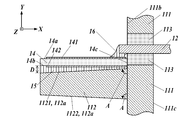
- FIG. 2 is a cross-sectional view of the electronic component mounting package 100 on a plane including the signal line 12 and perpendicular to the first surface 111b.
- the outer shape of the protrusion 112 in a side view as seen from the direction (Z direction) along the line in which the second surface 112a contacts the first surface 111b is the same as that of the protrusion 112 in the cross-sectional view of FIG. Corresponds to the outer shape. Therefore, in the present embodiment and other modifications described later, the shape of the protrusion 112 in the side view will be described with reference to the sectional view of FIG.
- the second surface 112a includes a portion that is inclined with respect to the first surface 111b in a side view when the second surface 112a is viewed from a direction along a line in contact with the first surface 111b.
- the second surface 112a includes a portion that is inclined with respect to the first surface 111b.
- the line where the second surface 112a contacts the first surface 111b can be said to be the root of the protrusion 112.
- the protrusion 112 has a surface 1121 located on the wiring board 14 side and a surface 1122 located on the opposite side of the surface 1121. It should be noted that each of the surfaces 1121 and 1122 is linear in a side view (cross-sectional view).
- the surface 1121 is a flat surface and the surface 1122 is a curved surface.
- the plane surface 1121 (second surface 112a) is entirely inclined with respect to the first surface 111b at the same angle, including the surface region bonded to the wiring board 14 via the bonding material 15. ing. That is, the rising angle A of the surface 1121 (second surface 112a) of the protrusion 112 from the first surface 111b is smaller than 90 degrees.
- the angle A mentioned here is, for example, an internal angle of the protrusion 112, that is, an angle formed by the second surface 112a with respect to the first surface 111b inside the base 11.
- the surface 1122 of the protrusion 112 opposite to the surface 1121 joined to the joining material 15 may also be inclined with respect to the first surface 111b. That is, both the surface 1121 and the surface 1122 of the protrusion 112 may be inclined with respect to the first surface 111b. In other words, the protrusion 112 may have a smaller thickness as the distance from the first surface 111b, that is, the root of the protrusion 112, increases.
- the angle A may be 60 degrees or more and less than 90 degrees.
- the inclination angle of the second surface 112a with respect to the direction perpendicular to the first surface 111b (X direction) may be greater than 0 degrees and 30 degrees or less.
- the surface 1121 of the protrusion 112 on the wiring substrate 14 side and the surface 1122 located on the opposite side of the wiring substrate 14 may also be inclined. That is, the surfaces 1121 and 1122 on both sides of the protrusion 112 may be the second surface 112a that is inclined with respect to the first surface 111b.
- the third surface 14a and the fourth surface 14b of the wiring board 14 are perpendicular to the first surface 111b. That is, in FIG. 2, the third surface 14a and the fourth surface 14b are located along a direction (X direction) perpendicular to the first surface 111b located along the Y direction. Therefore, the distance D between the protrusion 112 and the wiring board 14 increases as the second surface 112a, which is the root of the protrusion 112, moves away from the portion in contact with the first surface 111b. Accordingly, the thickness of the bonding material 15 increases as the distance from the root of the protrusion 112 increases.
- the distance D is, for example, the distance between the protrusion 112 and the wiring board 14 in the direction perpendicular to the fourth surface 14b, or the protrusion 112 in the direction perpendicular to the second surface 112a. It may be the distance between the wiring board 14 and the wiring board 14. Further, in the present embodiment, this distance D corresponds to the thickness of the bonding material 15.
- the bonding material 15 may have a thermal conductivity higher than that of the base 11.
- the heat generated by the operation of the electronic component 200 locally located on the wiring board 14 is transferred to the bonding material 15 via the wiring board 14 and then quickly diffuses in the bonding material 15.
- the thickness of the bonding material 15 is thick at a position close to the electronic component 200, that is, at a position away from the root of the projection 112, and thin at the root.
- the bonding material 15 has a large heat capacity in the portion close to the electronic component 200. Therefore, the heat transferred from the electronic component 200 and the wiring board 14 to the bonding material 15 is efficiently dispersed in the thickness direction, that is, downward in FIG. 2, and in the root direction, that is, rightward in FIG. It spreads over a wide area and is quickly released. As a result, the bonding material 15 is unlikely to be locally heated to a high temperature, and heat is efficiently exhausted from the electronic component 200.
- the uneven distribution of the temperature distribution in the bonding material 15 is small, the unevenness of the thermal expansion of the bonding material 15 depending on the temperature becomes smaller. As a result, it becomes difficult for an excessive force to be applied to the bonding material 15, the wiring board 14, and the base 11.
- such a shape and positional relationship is also effective when the wiring board 14 is bonded to the protrusion 112 via the bonding material 15.
- the bonding material 15 is hardened by being heated and bonded to the wiring board 14 and the protrusion 112.
- the bonding material 15 is heated, the protrusion 112 is heated, but since the contact area between the protrusion 112 and the bonding material 15 is larger than in the conventional case, heat is easily transferred to the entire bonding material 15.
- the exposed surface of the bonding material 15 that is, the part of the surface area of the bonding material 15 that is not in contact with the protrusion 112, the base 111, or the wiring board 14. Area increases.
- the organic solvent in the bonding material 15 easily volatilizes from the exposed surface, and the organic solvent is hardened more quickly and becomes a stable bonded state.
- the base 11 may be formed by driving a metal mold having a flat surface portion corresponding to the base portion 111 and a concave portion corresponding to the protrusion portion 112 into a metal base member.
- the metal base member is thinly rolled in the flat portion, while the metal base member is partially raised so as to fill the concave portion.
- the base 11 having the protrusion 112 joined to the base 111 is obtained.
- the concave portion is recessed perpendicular to the plane, a large force is likely to be applied to the corner located at the boundary between the concave portion and the plane portion, and wear of the mold or cutting tool is likely to occur.
- the concave part of the mold has a tapered shape corresponding to the above-mentioned protrusion 112, the force applied to this corner is dispersed to the periphery and wear of the mold, cutting tool, etc. Is reduced.
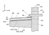
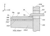
- FIG. 3A, 3B, 4A, and 4B are cross-sectional views of modified examples of the electronic component mounting package 100. More specifically, FIG. 3A, FIG. 3B, FIG. 4A, and FIG. 4B are cross-sectional views of the modified example corresponding to FIG. 2 of the electronic component mounting package 100.
- the thickness of the bonding material 15v1 may not be changed according to the distance from the first surface 111b. That is, in the electronic component mounting package 100 of Modification 1, the third surface 14a and the fourth surface 14b of the wiring board 14 may be inclined with respect to the first surface 111b. In the present modification, the third surface 14a and the fourth surface 14b of the wiring board 14 may be parallel to the surface 1121 of the protrusion 112.
- Such an electronic component mounting package 100 may be used when the mounting direction of the electronic component 200 does not need to be strictly determined.
- the second surface 112av2 of the protrusion 112v2 may have a curved shape instead of a flat surface, as in the electronic component mounting package 100 of the second modification shown in FIG. 3B.
- the second surface 112av2 is bent so that the protrusion 112v2 is convex outward. That is, as shown in FIG. 3B, the surfaces 1121 and 1122 (second surface 112av2) are curved lines in the side view (cross-sectional view).
- the second surface 112av2 is a curved surface whose inclination increases as it approaches the first surface 111b, and which is 90 degrees, that is, asymptotic to the direction perpendicular to the first surface 111b.
- the thickness of the bonding material 15v2 changes according to the distance from the first surface 111b so that the third surface 14a and the fourth surface 14b are perpendicular to the first surface 111b.
- the protrusion 112v3 may be provided.
- the second surface 112av3 that is inclined with respect to the first surface 111b is the surface 1122 on the side opposite to the wiring board 14. That is, in the protrusion 112, the surface 1121 on the wiring substrate 14 side may not be inclined with respect to the first surface 111b. That is, the surface 1121 of the protrusion 112 may be perpendicular to the first surface 111b.
- the bonding material 15v3 has the same thickness regardless of the distance from the first surface 111b, and the third surface 14a and the fourth surface 14b of the wiring board 14 are also formed on the first surface 111b. It is perpendicular to it.
- both the surface 1121 on the side of the wiring board 14 and the surface 1122 on the opposite side are the second surfaces 112a, 112av2 that are inclined with respect to the first surface 111b.
- only the surface 1121 on the wiring board 14 side may be inclined with respect to the first surface 111b, and the surface 1122 on the opposite side to the wiring board 14 may be perpendicular to the first surface 111b.
- the thickness of the wiring board 14 and the protruding portion 112 is changed according to the distance from the first surface 111b instead of the bonding material 15.
- Different plate members 15v4 may be located.
- the plate member 15v4 may have a thermal conductivity higher than that of the base 11, and is, for example, a copper plate, but is not limited to a conductor plate.
- the plate member 15v4 is joined to the wiring board 14 and the protrusion 112 using a joining member (not shown) or the like. In this case, the joining member may be sufficiently thin, and is not limited to the one satisfying the above conditions regarding viscosity and the like.
- the electronic component mounting package 100 of the present embodiment includes the base portion 111 having the first surface 111b and the protruding portion 112 having the second surface 112a protruding from the first surface 111b and in contact with the first surface.
- a base body 11 is included.
- the second surface 112a includes a portion in which the interior angle that is an angle formed with the first surface 111b is inclined less than 90 degrees.
- the protrusion 112 includes a portion whose thickness decreases as the distance from the first surface 111b increases in a side view seen from the direction along the line in which the second surface 112a contacts the first surface 111b.
- the protrusion 112 does not rise vertically from the base 111 but gradually rises, so that it is possible to reduce the load on a manufacturing tool or a tool related to the formation of the base 11, such as a mold or a cutting tool. .. Therefore, it is possible to prolong the life of a manufacturing tool such as a mold or a tool, and to mass-produce the electronic component mounting package 100 more efficiently.
- the entire second surface 112a is inclined at an angle of less than 90 degrees with respect to the first surface 111b, but the configuration of the second surface 112a is not limited to this.
- the second surface 112a may have at least a portion that is not in contact with the first surface 111b and has an angle of less than 90° with respect to the first surface 111b. Even with the protrusion 112 having such a shape, the above effect can be obtained.
- the electronic component mounting package 100 may further include the wiring board 14 on the second surface 112a. That is, in the protrusion 112, the surface to be joined to the wiring board 14 is formed to be inclined with respect to the first surface 111b, so that abrasion of a mold or the like during the formation is reduced and the accuracy is improved for a longer period of time.
- the second surface 112a can be obtained.
- the electronic component mounting package 100 further includes a bonding material 15 that is located between the wiring board 14 and the second surface 112a of the protrusion 112 and is bonded to the wiring board 14 and the second surface 112a.
- a bonding material 15 that is located between the wiring board 14 and the second surface 112a of the protrusion 112 and is bonded to the wiring board 14 and the second surface 112a.
- the electronic component mounting package 100 has a conductor surface in contact with the surface of the wiring board 14 on the side of the ground pattern 142, which is the surface on the opposite side of the wiring pattern 141, and the wiring for the base 11 including the protrusion 112.
- the distance from the wiring pattern 141 to the conductor surface can be appropriately determined regardless of the mounting angle of the substrate 14.
- the thickness of the bonding material 15 may be increased as the distance from the connecting portion (root) of the first surface 111b and the second surface 112a is increased. Accordingly, when the bonding material 15 is heated to bond the wiring board 14, the organic solvent in the bonding material 15 can be easily volatilized and diffused from the exposed portion. In addition, since the heat capacity increases near the tip of the wiring board 14, that is, at a position away from the first surface 111b, the heat generated by the electronic component located near the tip can be absorbed and the heat can be effectively dissipated. it can.
- the bonding material 15 may have a thermal conductivity higher than that of the base 11. Thereby, the heat generated by the electronic component 200 can be more efficiently released to the wide range of the base 11. As a result, it is possible to reduce the possibility that the electronic component 200 is overheated or the temperature of the electronic component mounting package 100 is locally increased.
- the bonding material 15 may be a nanoparticle sintering type bonding material paste.
- the nanoparticle-sintering-type bonding material paste here means the state after being fixed. Therefore, the joining material 15 can be suitably joined to both the conductor base 11 and the insulating wiring board 14. Moreover, since the bonding material 15 has an appropriate viscosity, the wiring board 14 can be fixed to the first surface 111b at an appropriate thickness and angle.
- the wiring board 14 may include a third surface 14a which is located on the side opposite to the second surface 112a and which is perpendicular to the first surface 111b. As described above, even in the form in which the protrusion 112 does not vertically project from the first surface 111b, the third surface 14a and the fourth surface 14b of the wiring board 14 are positioned perpendicular to the first surface 111b. By doing so, the orientation of the electronic component 200 can be easily determined based on the first surface 111b.
- the electronic device 1 of the present embodiment includes the electronic component mounting package 100 and the electronic component 200 described above.
- the electronic component 200 is mounted on the wiring board 14. Since the electronic device 1 can reduce abrasion of a mold, a cutting tool, and the like at the time of manufacturing more than before, it is possible to reduce the manufacturing cost while maintaining the accuracy of the shape.
- the base body 11 of the present embodiment includes the base portion 111 having the first surface 111b, and the protrusion portion 112 having the second surface 112a protruding from the first surface 111b. Then, the second surface 112a includes a portion whose angle formed with respect to the first surface 111b, that is, an inner angle is less than 90 degrees.
- the wiring board 14 is located on the protrusion 112.
- the above embodiment is an example, and various modifications can be made.
- the case where the protrusion 112 is formed using a mold has been described, but the present invention is not limited to this.
- the concave portion may be formed using a cutting tool or the like. Even in this case, it is possible to reduce the load on the cutting tool, etc. by forming a concave portion having an inclination such as a taper shape, rather than forming a vertical concave portion, and reduce the wear of the cutting tool and extend the life. Can be made.
- the second surface 112a is a flat surface or a curved surface in the above-described embodiment, the second surface 112a may have a bend at a position at a predetermined distance from the root of the protrusion 112. In this case, even in a shape in which the angle A is smaller than 90 degrees in a part of the second surface 112a, that is, in a shape including a part in which the thickness becomes smaller as the distance from the first surface 111b becomes larger in a part of the protrusion 112. Good.
- the second surface 112a may be a combination of a flat surface and a curved surface. That is, in the side view (cross-sectional view), the second surface 112a may be a combination of straight lines and curved lines.
- the bonding material 15 has been described as having a thermal conductivity higher than that of the base body 11.
- the bonding material 15 may have a thermal conductivity equal to or lower than that of the base body 11.
- the third surface 14a of the wiring substrate 14 including the wiring pattern 141 is perpendicular to the first surface 111b and the case where the third surface 14a is parallel to the second surface 112a. It is not limited to these.
- the third surface 14a including the wiring pattern 141 may be positioned at an appropriate angle with respect to the first surface 111b and the like depending on conditions such as the shape and orientation of the electronic component 200.
- the bonding material 15 is the nanoparticle sintering type bonding material paste
- the invention is not limited to this.
- the bonding material 15 when it is a thin film layer having a uniform thickness, it may simply be a conductive thin film layer.
- the bonding material 15 has high conductivity due to the bonding of the metals at the time of fixing, but the insulating bonding material is used to connect the wiring board 14 and the projection 112 via the ground pattern 142. And may be joined. Even in this case, as the bonding material, one having higher thermal conductivity than that of the protrusion 112 may be used. When the bonding material is not conductive, the ground pattern 142 may be electrically bonded to the base 111 of the base 11 that is a conductor.
- the number of protrusions, wiring boards, and electronic components in the electronic device of this embodiment is not limited to one each.
- the angle formed by the first surface and the second surface may be different for each protrusion.
- the electronic component mounting package 100 may be manufactured and traded separately from the electronic component 200.
- the specific details such as the structure, the material, and the positional relationship can be appropriately changed without departing from the spirit of the present invention.
- the present disclosure can be used for a base of an electronic component mounting package, an electronic device, and an electronic component mounting package.
Landscapes
- Cooling Or The Like Of Semiconductors Or Solid State Devices (AREA)
Abstract
本開示は、電子部品搭載用パッケージ、電子装置及び電子部品搭載用パッケージの基体を提供する。電子部品搭載用パッケージは、第1面を有する基部と、第1面から突出し第1面に接する第2面を有する突起部とを含む基体を備える。第2面は、第1面に対してなす角が90度未満に傾斜している部分を含む。
Description
本開示は、電子部品搭載用パッケージ、電子装置及び電子部品搭載用パッケージの基体に関する。
電子部品と接合される配線パターンを有する配線基板と、当該配線基板と接合している基体とを有する電子部品搭載用パッケージがある。このパッケージでは、特開2004-335584号公報などに示すように、基体は、基部と基部から垂直な方向に突出した突起形状を有する突起部とを有しており、配線基板は、基体の突起部上に位置する。これにより、配線基板上に位置する電子部品と基体との位置関係が明確になる。
本開示の一の態様は、
第1面を有する基部と、前記第1面から突出し前記第1面に接する第2面を有する突起部とを含む基体を備え、
前記第2面は、前記第1面に対してなす角が90度未満に傾斜している部分を含む、
電子部品搭載用パッケージである。
第1面を有する基部と、前記第1面から突出し前記第1面に接する第2面を有する突起部とを含む基体を備え、
前記第2面は、前記第1面に対してなす角が90度未満に傾斜している部分を含む、
電子部品搭載用パッケージである。
また、本開示の他の一の態様は、
上述の電子部品搭載用パッケージと、
電子部品と、
を備える電子装置である。
上述の電子部品搭載用パッケージと、
電子部品と、
を備える電子装置である。
また、本開示の他の一の態様は、
第1面を有する基部と、
前記第1面から突出し前記第1面と接する第2面を有する突起部と、
を含み、
前記第2面は、前記第1面に対してなす角が90度未満に傾斜している部分を含む、
電子部品搭載用パッケージの基体である。
第1面を有する基部と、
前記第1面から突出し前記第1面と接する第2面を有する突起部と、
を含み、
前記第2面は、前記第1面に対してなす角が90度未満に傾斜している部分を含む、
電子部品搭載用パッケージの基体である。
以下、実施の形態を図面に基づいて説明する。
図1は、本実施形態の電子装置1の全体斜視図である。
図1は、本実施形態の電子装置1の全体斜視図である。
電子装置1は、電子部品搭載用パッケージ100と、電子部品200とを備える。
電子部品搭載用パッケージ100は、基体11と、信号線12と、配線基板14と、接合材15と、導電性接合材16などを備える。
電子部品搭載用パッケージ100は、基体11と、信号線12と、配線基板14と、接合材15と、導電性接合材16などを備える。
基体11は、導電性の金属であり、接地面として機能する。基体11には、熱伝導率の高いものが用いられてよい。すなわち、基体11は、電子部品200から基体11に熱が伝わることで電子部品200の過熱を防ぐヒートシンクとしての機能を有する。基体11は、基部111と、突起部112とを有する。基部111は、ここでは、例えば、直径が3~10mm、厚さが0.5~2.0mmの円板状形状を有していてよいが、これには限られない。基部111は、貫通孔111aを有する。貫通孔111a内は、絶縁部材113により占められている。絶縁部材113は、例えば、ガラス又はセラミック材であってよい。絶縁部材113の材質及び貫通孔111aの大きさは、信号線12による信号伝送に係る所望の特性インピーダンスに応じて定められればよい。基部111と突起部112は一体的であってよい。
突起部112は、基部111において貫通孔111aの一端を含む第1面111bから突出している。突起部112は、第1面111bに接する第2面112aを有する。当該第2面112aの面上、すなわち、図1において突起部112の上側の面1121上には、配線基板14が接合材15を介して接合して位置している。なお、本実施形態においては、突起部112は、後述する信号線12の延在方向(X方向)に軸線を有する円柱を半分にした形状、いわゆる半円柱形状である。
配線基板14は、図2に示すように、第3面14a、第4面14b及び第5面14cを含む。第3面14aは、配線パターン141を有する。第4面14bは、第3面14aの反対側であって、接地パターン142を有する。第5面14cは、これら第3面14a及び第4面14bと接し、第1面111bと対向する。ここでは、第5面14cは、第1面111bと接してもいる。配線基板14は、例えば、高周波線路基板として用いられてもよい。配線基板14は、平板状の絶縁板であり、例えば、樹脂であってもよい。ここでは、第3面14aは、第2面112aとは反対側に位置し、第4面14bに平行であってもよい。配線基板14の厚さ及び材質、特に比誘電率は、配線パターン141による信号伝送に係る所望の特性インピーダンスに応じて適宜決定されればよい。
配線パターン141は、第3面14a上に位置し、電子部品200と電気的に接続されて、当該電子部品200に電力及び信号を供給する。配線パターン141は、抵抗の小さい導体金属膜、ここでは、金(Au)薄膜であってよい。配線パターン141は、ここでは2箇所が導電性接合材16を介して信号線12と接合している。配線パターンの形状、長さ及び位置は、接続される電子部品200のサイズ及び端子位置に応じて適宜定められてよい。配線パターン141は、配線基板14により接合材15と隔てられている。すなわち、配線基板14上では、マイクロストリップラインにより信号が伝送される。
図2に示すように、接地パターン142は、第4面14b上に位置し、配線パターン141に対する接地面をなす。接地パターン142は、配線パターン141の形状に応じた種々の形状を有するものであってもよい。例えば、接地パターン142は、配線パターン141の上方から見て配線パターン141が位置する範囲を囲うように配置されたベタ電極であってもよい。なお、接地パターン142は、例えば、金(Au)薄膜である。
接合材15は、配線基板14を接合する際に厚さを適切に調節可能な材質のものである。このような材質としては、適度な粘性を有するもの、例えば、粘度が30~250[Pa・s-1]であるものが挙げられる。これよりも粘度が低いと、接合時に接合材15が流動して適正な形状を保つのが難しくなる。反対に、粘度が高すぎても接合材15の形状の調節がしづらくなる。また、接合材15は、導体である突起部112だけではなく、絶縁部材である配線基板14とも接合する。また、ここでは、接合材15は、基体11よりも熱伝導率が大きくてもよい。例えば、接合材15は、ナノ粒子焼結型接合材ペーストであってもよい。ナノ粒子焼結型接合材ペーストは、表面安定剤に覆われたナノサイズの金属粒子と、樹脂と、有機溶剤とが混在している。金属粒子としては、例えば、銀又は銅などが挙げられる。ナノ粒子焼結型接合材ペーストは、固着した後には、有機溶剤が揮発している。すなわち、ナノ粒子焼結型接合材ペーストは、金属粒子が活性化して当該金属粒子同士が反応して結合するとともに、金属粒子が金属面とも反応して固着する。この金属粒子同士の結合により、大きな熱伝導率が得られる。
信号線12は棒状の導体である。信号線12は、当該信号線12の延在方向(X方向)について基部111の第1面111bとは反対の面111cから突出していてもよい。信号線12は、外部配線などと電気的に接続されて、リード電極として用いられる。信号線12の直径は、例えば、0.1~1.0mm程度である。信号線12のうち少なくとも1本は、基体11の接地端子であり、基部111に直接接合している。その他の信号線12、ここでは、2本の信号線12は、基部111の貫通孔111a内の絶縁部材113のほぼ中央を貫いている。これにより、この2本の信号線12は、絶縁部材113の内部では、外側の基部111と隔てられている。すなわち、信号は、基部111内を同軸線路により伝送される。
貫通孔111a内を通るこれらの信号線12の先端は、第1面111bの側で露出している。これらの信号線12は、導電性接合材16を介して配線パターン141と電気的につながっている。信号線12と配線パターン141とは、直接接触していてもよいし、直接接触していなくてもよい。信号線12の第1面111bからの突出長は、適宜定められる。ここでいう信号線12の突起長とは、信号線12の第1面111bから突出する部分のX方向における寸法である。なお、信号線12は、第1面111bから突出していなくてもよい。
導電性接合材16は、第1面111bの信号線12と第3面14a上の配線パターン141とを電気的に接合する。導電性接合材16は、例えば、金すず(AuSn)といった半田である。あるいは、導電性接合材16は、接合材15が導電性を有する場合には、接合材15と同一の種類のものであってもよい。
破線で示す電子部品200は、配線パターン141を含む第3面14a上に位置している。そして、電子部品200は、直接及び/又はワイヤボンディングなどにより配線パターン141と接合して電気的に接続されて、配線基板14の第3面14a上に搭載されている。電子部品200は、例えば、レーザーダイオードである。あるいは、電子部品200としては、フォトダイオード、LED(Light Emitting Diode)又はペルチェ素子、各種センサ素子など種々のものが用いられてよい。電子部品200の動作に伴って生じた熱は、主に接合材15及び基体11を介して排出される。
突起部112、配線パターン141を有する配線基板14、及び電子部品200は、図示略のカバー部材を蓋体として、当該蓋体によって覆われて外部と隔離されてもよい。電子部品200が外部に光を出射したりする場合には、カバー部材が当該出射光の波長を透過させる材質の窓部を有していてもよい。
次に、基体11の形状と配線基板14についてより詳しく説明する。
図2は、信号線12を含み第1面111bに垂直な面における、電子部品搭載用パッケージ100の断面図である。なお、本実施形態においては、第2面112aが第1面111bに接する線に沿った方向(Z方向)からみた側面視における突起部112の外形は、図2の断面図における突起部112の外形に対応する。よって、本実施形態及び後述する他の変形例では、前記側面視における突起部112の形状に関し、図2の断面図を用いて説明する。
図2は、信号線12を含み第1面111bに垂直な面における、電子部品搭載用パッケージ100の断面図である。なお、本実施形態においては、第2面112aが第1面111bに接する線に沿った方向(Z方向)からみた側面視における突起部112の外形は、図2の断面図における突起部112の外形に対応する。よって、本実施形態及び後述する他の変形例では、前記側面視における突起部112の形状に関し、図2の断面図を用いて説明する。
第2面112aは、第2面112aが第1面111bに接する線に沿った方向から見た側面視で、第1面111bに対して斜めに傾斜している部分を含む。言い換えれば、図2の断面視において、第2面112aは、第1面111bに対して斜めに傾斜している部分を含む。ここで、第2面112aが第1面111bに接する線とは、突起部112の根元であるともいえる。
より具体的には、突起部112は、配線基板14の側に位置する面1121と、該面1121とは反対側に位置する面1122と、を有している。なお、面1121、1122は、側面視(断面視)においては、いずれも直線状である。しかしながら、本実施形態の突起部112は、上述したように半円柱形状であるため、面1121は平面であり、面1122は曲面である。ここでは、平面状の面1121(第2面112a)は、接合材15を介して配線基板14と接合している面領域を含む全体が、同一の角度で第1面111bに対して傾斜している。すなわち、突起部112における面1121(第2面112a)の第1面111bからの立ち上がりの角度Aは、90度よりも小さい。ここでいう角度Aは、例えば、突起部112の内角であり、すなわち、基体11の内部であって第1面111bに対する第2面112aのなす角度である。なお、90度はここでいう「傾斜」に含まれない。
また、ここでは、突起部112の接合材15と接合している面1121とは反対側の面1122も、同じように第1面111bに対して傾斜していてよい。すなわち、突起部112の面1121及び面1122の両方が、第1面111bに対して傾斜していてよい。言い換えれば、突起部112は、第1面111b、すなわち突起部112の根元からの距離が大きくなるほど厚みが小さくなっていてもよい。このとき、角度Aが小さくなるほど後述の金型や切削工具などの磨耗が低減されるが、基部111及び突起部112の形状、大きさ、並びにこれらの位置関係などに応じて可能な範囲で角度Aが定められればよい。ここでは例えば、角度Aは、60度以上90度未満であってよい。言い換えると、第1面111bに対して垂直な方向(X方向)に対する第2面112aの傾斜角は、0度より大きく30度以下であってよい。なお、ここでは、上述したように、突起部112の配線基板14の側の面1121と、配線基板14とは反対側に位置する面1122も傾斜していてよい。すなわち、突起部112の両側の面1121、1122が第1面111bに対して傾斜している第2面112aであってよい。
より具体的には、突起部112は、配線基板14の側に位置する面1121と、該面1121とは反対側に位置する面1122と、を有している。なお、面1121、1122は、側面視(断面視)においては、いずれも直線状である。しかしながら、本実施形態の突起部112は、上述したように半円柱形状であるため、面1121は平面であり、面1122は曲面である。ここでは、平面状の面1121(第2面112a)は、接合材15を介して配線基板14と接合している面領域を含む全体が、同一の角度で第1面111bに対して傾斜している。すなわち、突起部112における面1121(第2面112a)の第1面111bからの立ち上がりの角度Aは、90度よりも小さい。ここでいう角度Aは、例えば、突起部112の内角であり、すなわち、基体11の内部であって第1面111bに対する第2面112aのなす角度である。なお、90度はここでいう「傾斜」に含まれない。
また、ここでは、突起部112の接合材15と接合している面1121とは反対側の面1122も、同じように第1面111bに対して傾斜していてよい。すなわち、突起部112の面1121及び面1122の両方が、第1面111bに対して傾斜していてよい。言い換えれば、突起部112は、第1面111b、すなわち突起部112の根元からの距離が大きくなるほど厚みが小さくなっていてもよい。このとき、角度Aが小さくなるほど後述の金型や切削工具などの磨耗が低減されるが、基部111及び突起部112の形状、大きさ、並びにこれらの位置関係などに応じて可能な範囲で角度Aが定められればよい。ここでは例えば、角度Aは、60度以上90度未満であってよい。言い換えると、第1面111bに対して垂直な方向(X方向)に対する第2面112aの傾斜角は、0度より大きく30度以下であってよい。なお、ここでは、上述したように、突起部112の配線基板14の側の面1121と、配線基板14とは反対側に位置する面1122も傾斜していてよい。すなわち、突起部112の両側の面1121、1122が第1面111bに対して傾斜している第2面112aであってよい。
これに対し、配線基板14の第3面14a及び第4面14bは、第1面111bに対して垂直である。すなわち、図2において、第3面14a及び第4面14bは、Y方向に沿って位置する第1面111bに対して垂直な方向(X方向)に沿って位置する。よって、突起部112と配線基板14との間の距離Dは、突起部112の根元である第2面112aが第1面111bに接する部分から離れるに従って大きくなっている。これに応じて、接合材15は、突起部112の根元からの距離が大きくなるに従って厚みが大きくなっている。ここで、距離Dとは、例えば、第4面14bに垂直な方向についての、突起部112と配線基板14との間の距離、又は、第2面112aに垂直な方向についての、突起部112と配線基板14との間の距離であってもよい。そして、本実施形態においては、この距離Dは、接合材15の厚みに対応している。
上述のように、接合材15は、基体11よりも熱伝導率が大きくてもよい。この場合、配線基板14上に局所的に位置する電子部品200の動作により生じた熱は、配線基板14を経て接合材15に伝わった後、当該接合材15内で速やかに拡散する。特にここでは、接合材15の厚みは、電子部品200に近い位置、すなわち、突起部112の根元から離れた位置で厚く、根元で薄くなっている。これにより、接合材15は、電子部品200に近い部分での熱容量が大きい。したがって、電子部品200及び配線基板14から接合材15に伝わった熱は、厚み方向、すなわち図2で下向き、及び根元方向、すなわち図2で右向きに効率よく分散して、基体11の突起部112の広い面積範囲に伝わって速やかに逃がされる。これにより、接合材15が局所的に高温になりにくく、電子部品200からの排熱が効率よく行われる。
また、接合材15内での温度分布の偏りが小さいことにより、接合材15では、温度に応じた熱膨張のむらがより小さくなる。これにより、接合材15、配線基板14及び基体11に無理な力がかかりにくくなる。
また、このような形状及び位置関係は、突起部112に対し、接合材15を介して配線基板14を接合する場合にも効果的である。上述のように、接合材15としてナノ粒子焼結型接合材ペーストが用いられる場合、この接合材15は、加熱されることにより硬化して、配線基板14及び突起部112と接合する。接合材15を加熱する際には、突起部112を加熱するが、突起部112と接合材15の接触面積が従来よりも大きいので、接合材15の全体に熱が伝わりやすい。また、根元から離れるに従って接合材15の厚みが大きくなることで、当該接合材15の露出面、すなわち、接合材15の表面積のうち突起部112、基部111又は配線基板14と接触していない部分の面積が増大する。これにより、接合材15内の有機溶剤が当該露出面から揮発しやすくなり、より速やかに硬化して安定した接合状態となる。
次に、基体11の製造方法の一例について説明する。基体11は、基部111に対応する平面部分と突起部112に対応する凹状部分とを有する金型を金属ベース部材に打ち込むことで形成されてもよい。金型を打ち込むと、金属ベース部材は、平面部分で薄く圧延される一方で、凹状部分を充填するように一部が盛り上がる。これにより、基部111に接合した突起部112を有する基体11が得られる。
このとき、凹状部分が平面に対して垂直にくぼんでいると、当該凹状部分と平面部分の境界に位置する角部に大きな力がかかりやすく、金型や切削工具などの磨耗が生じやすい。上述の突起部112に対応して、金型の凹状部分が傾斜を有したテーパー形状となっている場合には、この角部にかかる力が周囲に分散されて金型や切削工具などの磨耗が低減される。
図3A、図3B、図4A及び図4Bは、電子部品搭載用パッケージ100の変形例の断面図である。より具体的には、図3A、図3B、図4A及び図4Bは、電子部品搭載用パッケージ100の図2に対応する、前記変形例の断面図である。
図3Aに示す変形例1の電子部品搭載用パッケージ100のように、接合材15v1の厚さを第1面111bからの距離に応じて変化させていなくてもよい。すなわち、この変形例1の電子部品搭載用パッケージ100では、配線基板14の第3面14a及び第4面14bが第1面111bに対して傾斜していてもよい。本変形例においては、配線基板14の第3面14a及び第4面14bは、突起部112の面1121と平行であってもよい。電子部品200の取り付け方向が厳密に定められる必要がない場合などには、このような電子部品搭載用パッケージ100であってもよい。
図3Aに示す変形例1の電子部品搭載用パッケージ100のように、接合材15v1の厚さを第1面111bからの距離に応じて変化させていなくてもよい。すなわち、この変形例1の電子部品搭載用パッケージ100では、配線基板14の第3面14a及び第4面14bが第1面111bに対して傾斜していてもよい。本変形例においては、配線基板14の第3面14a及び第4面14bは、突起部112の面1121と平行であってもよい。電子部品200の取り付け方向が厳密に定められる必要がない場合などには、このような電子部品搭載用パッケージ100であってもよい。
図3Bに示す変形例2の電子部品搭載用パッケージ100のように、突起部112v2の第2面112av2が平面ではなく、曲面形状を有していてもよい。ここでは、前記側面視(断面視)において、突起部112v2が外側に凸となるように第2面112av2が曲がっている。すなわち、図3Bに示すように、前記側面視(断面視)において、面1121、1122(第2面112av2)は曲線である。このとき、例えば、第2面112av2は、第1面111bに近づくにつれて傾斜が大きくなり、90度、すなわち第1面111bに垂直な向きに漸近する曲面である。なお、接合材15v2は、第3面14a及び第4面14bが第1面111bに対して垂直となるように、第1面111bからの距離に応じて厚さが変化している。
図4Aに示す変形例3の電子部品搭載用パッケージ100のように、突起部112v3を有していてもよい。当該突起部112v3において、第1面111bに対して傾斜している第2面112av3は、配線基板14とは反対側の面1122である。すなわち、突起部112において配線基板14の側の面1121が第1面111bに対して傾斜していなくてもよい。つまり、突起部112の面1121は、第1面111bに垂直であってもよい。これに伴い、本変形例においては、接合材15v3は、第1面111bからの距離にかかわらず等しい厚さであり、配線基板14の第3面14a及び第4面14bも第1面111bに対して垂直である。なお、上記の突起部112、112v2などにおいて、配線基板14の側の面1121及びその反対側の面1122の両方が第1面111bに対して傾斜している第2面112a、112av2である代わりに、配線基板14の側の面1121のみが第1面111bに対して傾斜しており、配線基板14とは反対側の面1122が第1面111bに対して垂直であってもよい。
図4Bに示す変形例4の電子部品搭載用パッケージ100のように、配線基板14と突起部112との間には、接合材15の代わりに、第1面111bからの距離に応じて厚さが異なる板部材15v4が位置していてもよい。板部材15v4は、熱伝導率が基体11よりも高いものであってよく、例えば、銅板であるが、導体板には限られない。板部材15v4は、図示略の接合部材などを用いて配線基板14及び突起部112に接合される。この場合の接合部材は十分に薄くてよく、粘度などに係る上記の条件を満たすものに限られなくてよい。
以上のように、本実施形態の電子部品搭載用パッケージ100は、第1面111bを有する基部111と、第1面111bから突出し前記第1面に接する第2面112aを有する突起部112とを含む基体11を備える。第2面112aは、第1面111bに対してなす角である内角が90度未満に傾斜している部分を含む。言い換えると、突起部112は、第2面112aが第1面111bに接する線に沿った方向から見た側面視で、第1面111bから距離が大きくなるほど厚みが小さくなる部分を含む。
このように、突起部112が基部111から垂直に立ち上がらず、徐々に立ち上がることで、基体11の形成に係る製造用具や工具、例えば、金型や切削工具などへの負荷を低減させることができる。したがって、金型などの製造用具や工具の寿命を延長させて、より効率的に電子部品搭載用パッケージ100を量産することができる。
なお、本実施形態においては、第2面112aの全体が、第1面111bに対してなす角が90度未満に傾斜しているが、第2面112aの構成はこれに限らない。第2面112aは、少なくとも、第1面111bに接していない側において、第1面111bに対してなす角が90°未満に傾斜している部分を有していればよい。このような形状の突起部112であっても、上記効果を奏すことができる。
このように、突起部112が基部111から垂直に立ち上がらず、徐々に立ち上がることで、基体11の形成に係る製造用具や工具、例えば、金型や切削工具などへの負荷を低減させることができる。したがって、金型などの製造用具や工具の寿命を延長させて、より効率的に電子部品搭載用パッケージ100を量産することができる。
なお、本実施形態においては、第2面112aの全体が、第1面111bに対してなす角が90度未満に傾斜しているが、第2面112aの構成はこれに限らない。第2面112aは、少なくとも、第1面111bに接していない側において、第1面111bに対してなす角が90°未満に傾斜している部分を有していればよい。このような形状の突起部112であっても、上記効果を奏すことができる。
また、電子部品搭載用パッケージ100は、第2面112a上に配線基板14をさらに備えていてもよい。
すなわち、突起部112において、配線基板14と接合される面が第1面111bに対して傾斜して形成されるので、形成時における金型などの磨耗を低減し、より長期間精度のよい第2面112aを得ることができる。
すなわち、突起部112において、配線基板14と接合される面が第1面111bに対して傾斜して形成されるので、形成時における金型などの磨耗を低減し、より長期間精度のよい第2面112aを得ることができる。
また、電子部品搭載用パッケージ100は、配線基板14と突起部112の第2面112aとの間に位置しこれら配線基板14及び第2面112aに接合している接合材15をさらに備えていてもよい。すなわち、配線基板14と突起部112とは、接合材15を介して接合している。よって、電子部品搭載用パッケージ100は、配線基板14の配線パターン141とは反対側の面である接地パターン142の側の面に接して導体面を有し、突起部112を含む基体11に対する配線基板14の取り付け角度などによらずに適切に配線パターン141から導体面までの距離を定めることができる。
また、接合材15の厚みは、第1面111bと第2面112aのつながっている部分(根元)からの距離が大きいほど大きくてもよい。これにより、接合材15を加熱して配線基板14を接合する際に、接合材15内の有機溶剤を露出部分から揮発、発散させやすくすることができる。また、配線基板14の先端付近、すなわち、第1面111bから離れた位置における熱容量が増大するので、当該先端付近に位置する電子部品の発する熱を吸収して効果的に熱を発散することができる。
また、接合材15は、基体11よりも熱伝導率が大きくてもよい。これにより、電子部品200が発する熱をより効率的に基体11の広い範囲に逃がすことができる。その結果、電子部品200の過熱や電子部品搭載用パッケージ100の局所的な温度上昇が生じる可能性を低減することができる。
また、接合材15は、ナノ粒子焼結型接合材ペーストであってもよい。ここでいうナノ粒子焼結型接合材ペーストは、固着した後の状態のものを意味する。したがって、接合材15が、導体の基体11と絶縁性の配線基板14のいずれにも好適に接合することができる。また、接合材15が、適度な粘性を有することにより、配線基板14を第1面111bに対して適切な厚み及び角度で固定することができる。
また、配線基板14は、第2面112aとは反対側に位置し第1面111bに対して垂直な第3面14aを含んでもよい。このように、突起部112が第1面111bから垂直に突出していない形態であっても、配線基板14の第3面14a及び第4面14bが第1面111bに対して垂直に位置していることで、電子部品200の向きを容易に第1面111bを基準として定めることができる。
また、本実施形態の電子装置1は、上述の電子部品搭載用パッケージ100と、電子部品200と、を備える。この電子部品200は、配線基板14に搭載されている。
この電子装置1は、製造時の金型や切削工具などの磨耗を従来よりも低減することができるので、形状の精度を維持しながら製造コストを低減させることができる。
この電子装置1は、製造時の金型や切削工具などの磨耗を従来よりも低減することができるので、形状の精度を維持しながら製造コストを低減させることができる。
また、本実施形態の基体11は、第1面111bを有する基部111と、第1面111bから突出し第2面112aを有する突起部112と、を含む。そして、第2面112aは、第1面111bに対してなす角、すなわち内角が90度未満に傾斜している部分を含む。ここで、配線基板14は、突起部112上に位置する。
このように、突起部112が基部111から垂直に立ち上がっていない形状の基体11によれば、基体11の形成に係る製造用具、例えば、金型や切削工具などへの負荷を低減させることができる。したがって、金型や切削工具などの製造用具の寿命を延長させて、より効率的に製造することが可能になる。
このように、突起部112が基部111から垂直に立ち上がっていない形状の基体11によれば、基体11の形成に係る製造用具、例えば、金型や切削工具などへの負荷を低減させることができる。したがって、金型や切削工具などの製造用具の寿命を延長させて、より効率的に製造することが可能になる。
なお、上記実施の形態は例示であり、様々な変更が可能である。
例えば、上記実施の形態では、金型を用いて突起部112を形成するものとして説明したが、これに限られない。切削工具などを用いて凹状部分を形成してもよい。この場合でも、垂直な凹状部分を形成するよりも、テーパー形状など傾斜を有する凹状部分を形成するほうが切削工具などに対する負荷を低減させることができ、当該切削工具の消耗を低減させて寿命を延長させることができる。
例えば、上記実施の形態では、金型を用いて突起部112を形成するものとして説明したが、これに限られない。切削工具などを用いて凹状部分を形成してもよい。この場合でも、垂直な凹状部分を形成するよりも、テーパー形状など傾斜を有する凹状部分を形成するほうが切削工具などに対する負荷を低減させることができ、当該切削工具の消耗を低減させて寿命を延長させることができる。
また、上記実施の形態では、第2面112aが平面又は曲面であったが、第2面112aは、突起部112の根元から所定の距離の位置に折れ曲がりを有していてもよい。この場合、第2面112aの一部において角度Aが90度より小さい形状、すなわち、突起部112の一部において第1面111bから距離が大きくなるほど厚みが小さくなる部分を含む形状であってもよい。例えば、第2面112aが、平面と曲面との組み合わせであってもよい。すなわち、前記側面視(断面視)において、第2面112aは、直線及び曲線の組合せであってもよい。
また、上記実施の形態では、接合材15の熱伝導率が基体11よりも大きいものとして説明したが、基体11と同等又は基体11よりも熱伝導率が低いものであってもよい。
また、上記実施の形態では、配線基板14の配線パターン141を含む第3面14aが第1面111bに垂直な場合と、第2面112aに平行な場合とを例に挙げて説明したが、これらに限られない。電子部品200の形状及び向きなどの条件に応じて、配線パターン141を含む第3面14aが第1面111bなどに対して適宜な角度で位置していてもよい。
また、上記実施の形態では、接合材15がナノ粒子焼結型接合材ペーストである場合を例に挙げて説明したが、これに限られるものではない。例えば、接合材15が均一な厚みの薄膜層であればよい場合には、単純に導体薄膜層であってもよい。
また、上記実施の形態では、接合材15は、固着時の金属同士の結合により導電性の高いものであったが、絶縁性の接合材により接地パターン142を介して配線基板14と突起部112とが接合していてもよい。この場合でも接合材は、熱伝導性が突起部112よりも高いものが用いられてよい。接合材が導電性でない場合には、接地パターン142は、導体である基体11の基部111と電気的に接合されていてよい。
また、本実施形態の電子装置における突起部、配線基板及び電子部品は、それぞれ1つに限られない。複数の突起部が設けられる場合には、突起部ごとに第1面と第2面のなす角度が異なっていてもよい。
また、上記実施の形態及び各変形例で示した構造の一部ずつが任意に組み合わせられたものであってもよい。また、電子部品搭載用パッケージ100は、電子部品200とは別個に製造及び取引されてよい。
その他、上記の構造、材質及び位置関係などの具体的な細部は、本発明の趣旨を逸脱しない範囲で適宜変更可能である。
その他、上記の構造、材質及び位置関係などの具体的な細部は、本発明の趣旨を逸脱しない範囲で適宜変更可能である。
本開示は、電子部品搭載用パッケージ、電子装置及び電子部品搭載用パッケージの基体に利用することができる。
1 電子装置
11 基体
12 信号線
14 配線基板
14a 第3面
14b 第4面
14c 第5面
141 配線パターン
142 接地パターン
15、15v1~15v3 接合材
15v4 板部材
16 導電性接合材
100 電子部品搭載用パッケージ
111 基部
111a 貫通孔
111b 第1面
112、112v2、112v3 突起部
112a、112av2、112av3 第2面
113 絶縁部材
200 電子部品
11 基体
12 信号線
14 配線基板
14a 第3面
14b 第4面
14c 第5面
141 配線パターン
142 接地パターン
15、15v1~15v3 接合材
15v4 板部材
16 導電性接合材
100 電子部品搭載用パッケージ
111 基部
111a 貫通孔
111b 第1面
112、112v2、112v3 突起部
112a、112av2、112av3 第2面
113 絶縁部材
200 電子部品
Claims (11)
- 第1面を有する基部と、前記第1面から突出し前記第1面に接する第2面を有する突起部とを含む基体を備え、
前記第2面は、前記第1面に対してなす角が90度未満に傾斜している部分を含む、
電子部品搭載用パッケージ。 - 第1面を有する基部と、前記第1面から突出し前記第1面に接する第2面を有する突起部とを含む基体を備え、
前記突起部は、前記第2面が前記第1面に接する線に沿った方向から見た側面視で、前記第1面から距離が大きくなるほど厚みが小さくなる部分を含む、
電子部品搭載用パッケージ。 - 前記第2面上に位置する配線基板をさらに備える、請求項1又は2記載の電子部品搭載用パッケージ。
- 前記配線基板及び前記第2面の間に位置し前記配線基板及び前記第2面に接合している接合材をさらに備える、
請求項3記載の電子部品搭載用パッケージ。 - 前記接合材の厚みは、前記第2面が前記第1面に接している部分からの距離が大きいほど大きい、請求項4記載の電子部品搭載用パッケージ。
- 前記接合材は、前記基体よりも熱伝導率が大きい、請求項4又は5記載の電子部品搭載用パッケージ。
- 前記接合材は、ナノ粒子焼結型接合材ペーストである、請求項6記載の電子部品搭載用パッケージ。
- 前記配線基板は、前記第2面とは反対側に位置し前記第1面に対して垂直な第3面を有する、請求項3~7のいずれか一項に記載の電子部品搭載用パッケージ。
- 請求項1~8のいずれか一項に記載の電子部品搭載用パッケージと、
電子部品と、
を備える電子装置。 - 前記電子部品搭載用パッケージは、前記第2面上に位置する配線基板をさらに備え、
前記電子部品は、前記配線基板に搭載されている、
請求項9記載の電子装置。 - 第1面を有する基部と、
前記第1面から突出し前記第1面と接する第2面を有する突起部と、
を含み、
前記第2面は、前記第1面に対してなす角が90度未満に傾斜している部分を含む、
電子部品搭載用パッケージの基体。
Applications Claiming Priority (2)
| Application Number | Priority Date | Filing Date | Title |
|---|---|---|---|
| JP2019015166A JP2022053548A (ja) | 2019-01-31 | 2019-01-31 | 電子部品搭載用パッケージ、電子装置及び電子部品搭載用パッケージの基体 |
| JP2019-015166 | 2019-01-31 |
Publications (1)
| Publication Number | Publication Date |
|---|---|
| WO2020158944A1 true WO2020158944A1 (ja) | 2020-08-06 |
Family
ID=71841043
Family Applications (1)
| Application Number | Title | Priority Date | Filing Date |
|---|---|---|---|
| PCT/JP2020/003788 Ceased WO2020158944A1 (ja) | 2019-01-31 | 2020-01-31 | 電子部品搭載用パッケージ、電子装置及び電子部品搭載用パッケージの基体 |
Country Status (2)
| Country | Link |
|---|---|
| JP (1) | JP2022053548A (ja) |
| WO (1) | WO2020158944A1 (ja) |
Citations (3)
| Publication number | Priority date | Publication date | Assignee | Title |
|---|---|---|---|---|
| JP2005223083A (ja) * | 2004-02-04 | 2005-08-18 | Sony Corp | 半導体装置 |
| JP2015082609A (ja) * | 2013-10-23 | 2015-04-27 | 新光電気工業株式会社 | 半導体パッケージ用ステム及び半導体パッケージ |
| JP2016092394A (ja) * | 2014-10-30 | 2016-05-23 | 京セラ株式会社 | 電子部品搭載用パッケージおよびそれを用いた電子装置 |
-
2019
- 2019-01-31 JP JP2019015166A patent/JP2022053548A/ja active Pending
-
2020
- 2020-01-31 WO PCT/JP2020/003788 patent/WO2020158944A1/ja not_active Ceased
Patent Citations (3)
| Publication number | Priority date | Publication date | Assignee | Title |
|---|---|---|---|---|
| JP2005223083A (ja) * | 2004-02-04 | 2005-08-18 | Sony Corp | 半導体装置 |
| JP2015082609A (ja) * | 2013-10-23 | 2015-04-27 | 新光電気工業株式会社 | 半導体パッケージ用ステム及び半導体パッケージ |
| JP2016092394A (ja) * | 2014-10-30 | 2016-05-23 | 京セラ株式会社 | 電子部品搭載用パッケージおよびそれを用いた電子装置 |
Also Published As
| Publication number | Publication date |
|---|---|
| JP2022053548A (ja) | 2022-04-06 |
Similar Documents
| Publication | Publication Date | Title |
|---|---|---|
| WO2021020480A1 (ja) | 電子素子搭載用パッケージ及び電子装置 | |
| JP4009208B2 (ja) | 発光装置 | |
| JP2006313896A (ja) | 発光素子パッケージ | |
| CN105359632B (zh) | 布线基板以及电子装置 | |
| JP2011018800A (ja) | 半導体レーザ装置 | |
| JP6754769B2 (ja) | 半導体モジュールおよびその製造方法 | |
| JP7170832B2 (ja) | 電子素子搭載用パッケージ及び電子装置 | |
| JP4383059B2 (ja) | 発光素子収納用パッケージおよび発光装置 | |
| JP2015122487A (ja) | 発光装置、発光装置製造方法 | |
| CN101299450A (zh) | 光发射器件及其制造方法 | |
| TW202040773A (zh) | 半導體裝置用管座和半導體裝置 | |
| WO2020158944A1 (ja) | 電子部品搭載用パッケージ、電子装置及び電子部品搭載用パッケージの基体 | |
| JP2022116383A (ja) | 電子素子搭載用パッケージ及び電子装置 | |
| JP5214121B2 (ja) | 発光装置 | |
| WO2020175619A1 (ja) | 電子部品搭載用パッケージ、電子装置及び発光装置 | |
| US12396093B2 (en) | Power supply module and power device | |
| JP2005223083A (ja) | 半導体装置 | |
| US11955769B2 (en) | Optical element mounting package, electronic device, and electronic module | |
| JP2005223083A5 (ja) | ||
| JP4177874B2 (ja) | 発光装置 | |
| WO2021020530A1 (ja) | 電子素子搭載用パッケージ及び電子装置 | |
| WO2020158928A1 (ja) | 電子部品搭載用パッケージ及び電子装置 | |
| CN113169138B (zh) | 载体,具有载体的装置和用于制造载体的方法 | |
| CN114270641A (zh) | 光元件搭载用封装件、电子装置及电子模块 | |
| JP2020188115A (ja) | 電子部品搭載用パッケージ及び電子装置 |
Legal Events
| Date | Code | Title | Description |
|---|---|---|---|
| 121 | Ep: the epo has been informed by wipo that ep was designated in this application |
Ref document number: 20748126 Country of ref document: EP Kind code of ref document: A1 |
|
| NENP | Non-entry into the national phase |
Ref country code: DE |
|
| 122 | Ep: pct application non-entry in european phase |
Ref document number: 20748126 Country of ref document: EP Kind code of ref document: A1 |
|
| NENP | Non-entry into the national phase |
Ref country code: JP |