WO2020158080A1 - 高調波処理回路及び増幅器 - Google Patents
高調波処理回路及び増幅器 Download PDFInfo
- Publication number
- WO2020158080A1 WO2020158080A1 PCT/JP2019/042186 JP2019042186W WO2020158080A1 WO 2020158080 A1 WO2020158080 A1 WO 2020158080A1 JP 2019042186 W JP2019042186 W JP 2019042186W WO 2020158080 A1 WO2020158080 A1 WO 2020158080A1
- Authority
- WO
- WIPO (PCT)
- Prior art keywords
- line
- harmonic
- impedance
- harmonic processing
- fundamental wave
- Prior art date
- Legal status (The legal status is an assumption and is not a legal conclusion. Google has not performed a legal analysis and makes no representation as to the accuracy of the status listed.)
- Ceased
Links
Images








Classifications
-
- H—ELECTRICITY
- H03—ELECTRONIC CIRCUITRY
- H03F—AMPLIFIERS
- H03F1/00—Details of amplifiers with only discharge tubes, only semiconductor devices or only unspecified devices as amplifying elements
- H03F1/02—Modifications of amplifiers to raise the efficiency, e.g. gliding Class A stages, use of an auxiliary oscillation
- H03F1/04—Modifications of amplifiers to raise the efficiency, e.g. gliding Class A stages, use of an auxiliary oscillation in discharge-tube amplifiers
- H03F1/06—Modifications of amplifiers to raise the efficiency, e.g. gliding Class A stages, use of an auxiliary oscillation in discharge-tube amplifiers to raise the efficiency of amplifying modulated radio frequency waves; to raise the efficiency of amplifiers acting also as modulators
- H03F1/07—Doherty-type amplifiers
-
- H—ELECTRICITY
- H03—ELECTRONIC CIRCUITRY
- H03F—AMPLIFIERS
- H03F1/00—Details of amplifiers with only discharge tubes, only semiconductor devices or only unspecified devices as amplifying elements
- H03F1/02—Modifications of amplifiers to raise the efficiency, e.g. gliding Class A stages, use of an auxiliary oscillation
- H03F1/0205—Modifications of amplifiers to raise the efficiency, e.g. gliding Class A stages, use of an auxiliary oscillation in transistor amplifiers
- H03F1/0288—Modifications of amplifiers to raise the efficiency, e.g. gliding Class A stages, use of an auxiliary oscillation in transistor amplifiers using a main and one or several auxiliary peaking amplifiers whereby the load is connected to the main amplifier using an impedance inverter, e.g. Doherty amplifiers
-
- H—ELECTRICITY
- H03—ELECTRONIC CIRCUITRY
- H03F—AMPLIFIERS
- H03F1/00—Details of amplifiers with only discharge tubes, only semiconductor devices or only unspecified devices as amplifying elements
- H03F1/56—Modifications of input or output impedances, not otherwise provided for
- H03F1/565—Modifications of input or output impedances, not otherwise provided for using inductive elements
-
- H—ELECTRICITY
- H03—ELECTRONIC CIRCUITRY
- H03F—AMPLIFIERS
- H03F3/00—Amplifiers with only discharge tubes or only semiconductor devices as amplifying elements
- H03F3/60—Amplifiers in which coupling networks have distributed constants, e.g. with waveguide resonators
- H03F3/601—Amplifiers in which coupling networks have distributed constants, e.g. with waveguide resonators using FET's, e.g. GaAs FET's
Definitions
- the present disclosure relates to a harmonic processing circuit and an amplifier.
- This application claims the priority right based on Japanese application No. 2019-012992 filed on January 29, 2019, and incorporates all the contents described in the above Japanese application.
- a harmonic processing circuit is a power supply line for supplying power to an amplification element, and a harmonic processing that is connected to the power supply line and performs harmonic processing at a harmonic frequency of a signal output from the amplification element. And a feed line that is connected to the amplification element and is connected to a fundamental wave matching circuit that performs matching at the fundamental wave frequency of the signal.
- An amplifier is an amplification element, a power supply line for supplying power to the amplification element, and is connected to the power supply line, and performs harmonic processing at a harmonic frequency of a signal output from the amplification element.
- a harmonics processing unit, and the feed line is connected to a fundamental wave matching circuit that is connected to the amplification element and performs matching at a fundamental frequency of the signal.
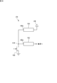
- FIG. 8 is a diagram showing a circuit in which a harmonic processing circuit is provided in the power supply line.
- a fundamental wave matching circuit 102 that performs impedance matching of a fundamental wave included in a signal output by the amplification element 100 is connected to a drain terminal of the amplification element 100.
- the power supply line 104 connects the drain terminal of the amplification element 100 and the DC power supply 106.
- a harmonic processing unit 108 that performs harmonic processing of the signal is connected to the power supply line 104.
- the load impedance of the harmonic frequency in the fundamental matching circuit 102 is not taken into consideration in the fundamental matching circuit 102, the load impedance of the harmonic frequency when the terminal 102 a of the fundamental matching circuit 102 is viewed from the connecting portion 110.
- the impedance may be near the short circuit.
- a harmonic processing circuit is connected to a power feeding line for feeding power to an amplification element, and performs harmonic processing at a harmonic frequency of a signal output from the amplification element.
- a harmonics processing unit, and the feed line is connected to a fundamental wave matching circuit that is connected to the amplification element and performs matching at a fundamental frequency of the signal.
- the power feeding line since the power feeding line is connected to the fundamental wave matching circuit, the power feeding line can be connected to any position within the line length of the fundamental wave matching circuit. Therefore, it is possible to adjust the impedance of the harmonic frequency when the fundamental wave matching circuit is viewed from the connecting portion to which the power feeding line is connected so as not to be short-circuited. As a result, the load impedance of the harmonic frequency when the load side is viewed from the amplification element can be adjusted by the impedance of the harmonic frequency set in the harmonic processing unit, and the harmonic processing can be appropriately performed. ..
- the fundamental wave matching circuit includes a signal line whose one end is connected to the amplification element, and the feed line has a line length from one end of the signal line that is a predetermined length. Preferably, it is connected to the salient position. In this case, by adjusting the position of the connection portion of the power supply line, it is possible to adjust so that the impedance of the harmonic frequency when the other end side portion of the signal line is viewed from the connection portion of the power supply line does not become a short circuit. ..
- the distributor 6 is connected to the subsequent stage of the input terminal 2 and distributes the RF signal supplied from the input terminal 2 to the carrier amplifier 4 and the peak amplifier 5.
- the output of the distributor 6 is given to the carrier amplifier 4 via the carrier side input matching circuit 8 and to the peak amplifier 5 via the peak side input matching circuit 9.
- the carrier side input matching circuit 8 performs impedance matching between the distributor 6 side and the carrier amplifier 4 side at the frequency of the fundamental wave included in the input of the carrier amplifier 4.
- the peak-side input matching circuit 9 performs impedance matching between the distributor 6 side and the peak amplifier 5 side at the frequency of the fundamental wave included in the input of the peak amplifier 5.
- the output of the carrier amplifier 4 is given to the combiner 7 via the carrier side output matching circuit 10.
- the output of the peak amplifier 5 is given to the combiner 7 via the peak side output matching circuit 11.
- the carrier-side output matching circuit 10 is a circuit for converting the impedance (load impedance) of the carrier amplifier 4 when looking at the load-side combiner 7 side into a desired impedance.
- the carrier-side output matching circuit 10 performs impedance matching for converting the load impedance into a desired impedance for the frequency of the fundamental wave of the signal output from the carrier amplifier 4.
- the Doherty amplifier 1 is connected to a first drain power source 30, a second drain power source 40, a first gate power source 60, and a second gate power source 70 provided outside the circuit board 25.
- the first drain power supply 30 is a DC power supply for supplying power to the drain terminal of the carrier amplifier 4, and is connected to the carrier-side output matching circuit 10 via the first power supply line 31.
- the second drain power supply 40 is a DC power supply for supplying power to the drain terminal of the peak amplifier 5, and is connected to the peak side output matching circuit 11 via the second power supply line 41.
- the first gate power supply 60 is a DC power supply for supplying power to the gate terminal of the carrier amplifier 4, and is connected to the gate terminal of the carrier amplifier 4 via the third power supply line 61.
- the second gate power supply 70 is a DC power supply for supplying power to the gate terminal of the peak amplifier 5, and is connected to the gate terminal of the peak amplifier 5 via the fourth power supply line 71.
- the first feeding line 31 and the first harmonic processing unit 32 connected to the first feeding line 31 configure a first harmonic processing circuit 33.
- the first harmonic processing circuit 33 is a circuit for converting the load impedance of the harmonic frequency when the combiner 7 side, which is the load side, is viewed from the carrier amplifier 4 into a desired impedance.
- the process of converting the load impedance of the harmonic frequency into a desired impedance is the harmonic process.
- the second power feeding line 41 and the second harmonic processing unit 42 connected to the second power feeding line 41 configure a second harmonic processing circuit 43.
- the second harmonic processing circuit 43 is also similar to the first harmonic processing circuit 33, and converts the load impedance of the harmonic frequency when the combiner 7 side, which is the load side, is viewed from the peak amplifier 5 into a desired impedance. It is a circuit for doing.
- the first feeder line 31 of the present embodiment is connected to the carrier side output matching circuit 10.
- the carrier side output matching circuit 10 is configured to include a first line 21 and a second line 22.
- One end 21 a of the first line 21 is connected to the carrier amplifier 4.
- the other end 21b of the first line 21 is connected to one end 22a of the second line 22.
- the other end of the second line 22 is connected to the combiner 7.
- the first feeding line 31 is connected to the connecting portion 23 that connects the first line 21 and the second line 22.
- the line length of the first line 21 is set in the range of ⁇ /16 or more and 3 ⁇ /16 or less, where ⁇ is the wavelength of the fundamental wave.
- ⁇ is the wavelength of the fundamental wave.
- the phase angle of the impedance of the carrier-side output matching circuit 10 with respect to the second harmonic can be changed within the range of about 90 degrees to about 270 degrees. Therefore, if the line length of the first line 21 is set within the above range, it is possible to surely perform adjustment so that the impedance of the harmonic frequency when the second line 22 is viewed from the connecting portion 23 does not become a short circuit. ..
- FIG. 3A shows the impedance when the harmonic processing circuit 33 is seen from the connection portion 23, and FIG. 3B shows the impedance when the one end 22 a of the second line 22 is seen from the connection portion 23.
- the impedance of the fundamental wave frequency f 0 is almost open as described above.
- the impedance of the second harmonic frequency 2f 0 is almost open.
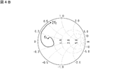
- FIG. 4A shows the impedance when the connection portion 23 is seen from the other end 21b of the first line 21, and FIG. 4B shows the impedance when the one end 21a of the carrier side output matching circuit 10 is seen from the carrier amplifier 4. Is shown. Comparing the impedance shown in FIG. 4A and the impedance shown in FIG. 3A, the two show different characteristics from each other. Further, when the impedance shown in FIG. 4A and the impedance shown in FIG. 3B are compared, the two show characteristics different from each other.
- the characteristics regarding the saturation power and efficiency of the amplification element used in the example were grasped by the load pull measurement, and based on the result, the target impedance to be converted by the fundamental wave matching circuit and the harmonic processing circuit was specified.
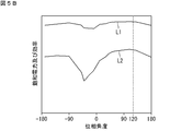
- FIG. 5B is a graph showing the measurement result of the characteristics regarding the saturation power and the efficiency with respect to the second harmonic in the amplification element.
- the horizontal axis represents the phase angle
- the vertical axis represents the saturation power and the efficiency.
- the line L1 shows the saturation power
- the line L2 shows the efficiency. From this graph, the phase angle at which the saturated power and the efficiency are the highest was specified and used as the target phase angle of the second harmonic frequency.
- the target phase angle of the second harmonic frequency is set to 120 degrees.
- FIG. 6B shows one end 225a of the fundamental wave matching circuit 210 seen from the amplification element when one end 225a of the fundamental wave matching circuit 210 shown in FIG. 6A is connected to the amplification element and a load of 50 ⁇ is connected to the other end 225b. It is a Smith chart which shows impedance at the time.
- the marker m1 indicates the impedance whose frequency is the fundamental wave frequency (3.8 GHz).
- the marker m2 indicates the impedance of the second harmonic frequency (7.6 GHz).
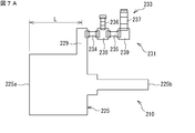
- the line 229 that connects the first inductance element 234 and the harmonic processing circuit 233 constitutes a part of the power feeding line 231, and connects the harmonic processing unit including each element and the harmonic processing circuit 233.
- the line 229 is connected to a position where the line length from the one end 225a of the signal line 225 is a predetermined length L.
- the predetermined length L in the embodiment is set to 5.2 mm. This predetermined length L corresponds to ⁇ /8, where ⁇ is the wavelength of the fundamental wave.
- FIG. 7B shows one end 225a of the fundamental wave matching circuit 210 shown in FIG. 7A when one end 225a of the fundamental wave matching circuit 210 is connected to an amplifying element and the other end 225b is connected to a load of 50 ⁇ . It is a Smith chart which shows impedance at the time.
- the marker m11 indicates the impedance whose frequency is the fundamental wave frequency (3.8 GHz).
- the marker m12 indicates the impedance of the second harmonic frequency (7.6 GHz).
- the fundamental wave matching circuit 210 and the harmonic processing circuit 233 are connected to the output terminal of the amplification element, even if it becomes difficult to adjust the load impedance of the harmonic frequency viewed from the amplification element, By connecting the harmonic processing circuit 233 to the fundamental wave matching circuit 210 as in the example, the load impedance at the harmonic frequency can be appropriately adjusted.
- the above-mentioned Doherty amplifier 1 is mounted in a wireless communication device such as a base station device in a mobile communication system and amplifies a transmission signal (RF signal) of a radio frequency. That is, the carrier amplifier 4 and the peak amplifier 5 included in the Doherty amplifier perform amplification of a radio frequency transmission modulation signal obtained by modulating a radio frequency carrier with transmission data. Therefore, the above description includes the features additionally described below.
- a feed line for feeding the amplification element A harmonic processing unit that is connected to the power supply line and performs a harmonic process at a harmonic frequency of a radio frequency transmission modulation signal output from the amplification element;
- the harmonic processing circuit wherein the power supply line is connected to the amplification element and is connected to a fundamental wave matching circuit that performs matching at the fundamental wave frequency of the transmission modulation signal.
Landscapes
- Engineering & Computer Science (AREA)
- Power Engineering (AREA)
- Amplifiers (AREA)
- Microwave Amplifiers (AREA)
Abstract
Description
本出願は、2019年1月29日出願の日本出願第2019-012992号に基づく優先権を主張し、前記日本出願に記載された全ての記載内容を援用するものである。
上記高調波処理回路に含まれるオープンスタブは、処理対象となる信号の波長に応じてその大きさが定まる。つまり、オープンスタブは、一定の大きさを確保する必要あるため、小型化が困難であるという問題を有している。
図8中、増幅素子100のドレイン端子には、増幅素子100が出力する信号に含まれる基本波のインピーダンス整合を行う基本波整合回路102が接続されている。
給電線路104は、増幅素子100のドレイン端子と、直流電源106とを接続している。給電線路104には、前記信号の高調波処理を行う高調波処理部108が接続されている。
基本波整合回路102は、増幅素子100の基本波周波数の負荷インピーダンスが最適となるように設定されるため、高調波周波数の負荷インピーダンスについては考慮されないことがある。
よって、高調波処理部108の端子108aにおける高調波周波数のインピーダンスは、基本波整合回路102の端子102aにおける高調波周波数のインピーダンスに応じて適切に設定される必要がある。
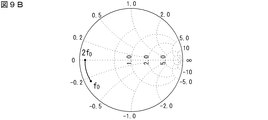
図9Aから図9Cには、信号の基本波周波数f0から2倍波周波数2f0まで変化させたときのインピーダンスを示している。
つまり、増幅素子100から見たときの負荷インピーダンスには、高調波処理部108による影響が及んでいないことが判る。
このため、適切に高調波処理を行うことができないおそれがあった。
本開示によれば、適切に高調波処理を行うことができる。
[実施形態の概要]
(1)一実施形態である高調波処理回路は、増幅素子に給電するための給電線路と、前記給電線路に接続され、前記増幅素子から出力される信号の高調波周波数における高調波処理を行う高調波処理部と、を備え、前記給電線路は、前記増幅素子に接続され前記信号の基本波周波数における整合を行う基本波整合回路に接続される。
よって、給電線路が接続される接続部から基本波整合回路を見たときの高調波周波数のインピーダンスがショートにならないように調整することができる。
この結果、増幅素子から負荷側を見たときの高調波周波数の負荷インピーダンスを、高調波処理部において設定される高調波周波数のインピーダンスによって調整が可能となり、適切に高調波処理を行うことができる。
この場合、第1線路の線路長を調整することで、接続部から第2線路を見たときの高調波周波数のインピーダンスがショートにならないように調整することができる。
この場合、接続部から第2線路を見たときの2次高調波におけるインピーダンスの位相角度を、基本波整合回路を増幅素子から見たときの2次高調波におけるインピーダンスに対して約90度から約270度まで変更することができる。
よって、第1線路の線路長を上記範囲内で設定すれば、接続部から第2線路を見たときの高調波周波数のインピーダンスがショートにならないような調整を確実に行うことができる。
この場合、給電線路の接続部の位置を調整することで、給電線路の接続部から信号線路の他端側部分を見たときの高調波周波数のインピーダンスがショートにならないように調整することができる。
この場合、例えば、給電線路の接続部から信号線路の他端側部分を見たときの2次高調波におけるインピーダンスの位相角度を、基本波整合回路を増幅素子から見たときの2次高調波におけるインピーダンスに対して約90度から約270度まで変更することができる。
よって、接続部から信号線路の他端側部分を見たときの高調波周波数のインピーダンスがショートにならないような調整を確実に行うことができる。
以下、好ましい実施形態について図面を参照しつつ説明する。
なお、以下に記載する各実施形態の少なくとも一部を任意に組み合わせてもよい。
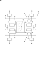
図1は、一実施形態に係るドハティ増幅器の構成を示すブロック図である。
このドハティ増幅器1は、移動体通信システムにおける基地局装置などの無線通信装置に搭載され、無線周波数の送信信号(RF信号)の増幅を行う。
ドハティ増幅器1は、入力端子2に与えられるRF信号(入力信号)を増幅し、出力端子3から出力する。
分配器6の出力は、キャリア側入力整合回路8を介してキャリアアンプ4へ与えられるとともに、ピーク側入力整合回路9を介してピークアンプ5へ与えられる。
キャリア側入力整合回路8は、分配器6側と、キャリアアンプ4側との間において、キャリアアンプ4の入力に含まれる基本波の周波数におけるインピーダンス整合を行う。また、ピーク側入力整合回路9は、分配器6側と、ピークアンプ5側との間において、ピークアンプ5の入力に含まれる基本波の周波数におけるインピーダンス整合を行う。
キャリアアンプ4、及びピークアンプ5は、一つの集積回路上に実装されており、一つのパッケージ12内に収容されている。
また、ピークアンプ5の出力は、ピーク側出力整合回路11を介して合成器7へ与えられる。
キャリア側出力整合回路10は、キャリアアンプ4から負荷側である合成器7側を見たときのインピーダンス(負荷インピーダンス)を所望のインピーダンスへ変換するための回路である。キャリア側出力整合回路10は、負荷インピーダンスを所望のインピーダンスへ変換するインピーダンス整合を、キャリアアンプ4が出力する信号の基本波の周波数について行う。
出力端子3は、合成器7から与えられた出力信号を出力する。
第1ドレイン電源30は、キャリアアンプ4のドレイン端子に給電するための直流電源であり、第1給電線路31を介してキャリア側出力整合回路10に接続されている。
第2ドレイン電源40は、ピークアンプ5のドレイン端子に給電するための直流電源であり、第2給電線路41を介してピーク側出力整合回路11に接続されている。
第2ゲート電源70は、ピークアンプ5のゲート端子に給電するための直流電源であり、第4給電線路71を介してピークアンプ5のゲート端子に接続されている。
また、第2給電線路41には、ピークアンプ5の出力に含まれる高調波の周波数における高調波処理を行うための機能を有する第2高調波処理部42が接続されている。
第1高調波処理回路33は、キャリアアンプ4から負荷側である合成器7側を見たときの高調波周波数の負荷インピーダンスを所望のインピーダンスへ変換するための回路である。高調波周波数の負荷インピーダンスを所望のインピーダンスへ変換する処理が、高調波処理である。
第2高調波処理回路43も、第1高調波処理回路33と同様であり、ピークアンプ5から負荷側である合成器7側を見たときの高調波周波数の負荷インピーダンスを所望のインピーダンスへ変換するための回路である。
図2に示すように、第1高調波処理回路33は、第1給電線路31と、第1高調波処理部32と、を含んで構成される。
上記各素子34,35,36,37は第1給電線路31に接続された集中定数素子であり、第1高調波処理部32は、集中定数回路を含んで構成されている。
第1容量素子36は、一端が第1インダクタンス素子34と第2インダクタンス素子35との間の接続点38に接続され、他端が接地されている。
第2容量素子37は、一端が第2インダクタンス素子35と第1ドレイン電源30との間の接続点39に接続され、他端が接地されている。
これにより、両アンプ4,5を有するドハティ増幅器1に高調波処理回路を設けたとしても、高調波処理回路の設置によって当該ドハティ増幅器1が大型化するのを抑制することができる。
この場合、第1高調波処理部32(第2高調波処理部42)が基本波に対して与える影響を抑制することができる。
これにより、給電線路の電源側へ高周波信号が漏洩するのを防止することができる。
このような関係を満たすように設定することで、第2容量素子37の容量や、その他の条件を満たしつつ、各素子の値を適切に設定することができる。
このため、第1インダクタンス素子34と、第2インダクタンス素子35との間に第1容量素子36を接続しない構成とすることができる場合がある。
キャリア側出力整合回路10は、第1線路21と、第2線路22とを含んで構成されている。
第1線路21の一端21aは、キャリアアンプ4に接続されている。第1線路21の他端21bは、第2線路22の一端22aに接続されている。
第2線路22の他端は合成器7に接続されている。
第1給電線路31は、第1線路21と第2線路22とを接続する接続部23に接続されている。
この場合、キャリア側出力整合回路10(の一端21a)を高調波処理回路33の接続部(キャリアアンプ4のドレイン端子)から見たときの2倍波周波数のインピーダンスがショート近傍であるとすると、第1高調波処理部32を調整し、第1高調波処理回路33が変換しようとする高調波周波数のインピーダンスを変更したとしても、キャリアアンプ4から見た負荷インピーダンスを所望の値に調整することが困難となる場合かあった。
よって、第1給電線路31(高調波処理回路33)が接続される接続部23からキャリア側出力整合回路10を見たときの高調波周波数のインピーダンスがショートにならないように調整することができる。
この結果、キャリアアンプ4から負荷側を見たときの高調波周波数の負荷インピーダンスを、第1高調波処理部32において設定される高調波周波数のインピーダンスによって調整が可能となる。
これにより、適切に高調波処理を行うことができる。
これにより、キャリア側出力整合回路10の2倍波に対するインピーダンスの位相角度を約90度から約270度の範囲で変更することができる。
よって、第1線路21の線路長を上記範囲内で設定すれば、接続部23から第2線路22を見たときの高調波周波数のインピーダンスがショートにならないような調整を確実に行うことができる。
図3Aにおいて、基本波周波数f0のインピーダンスは、上述したように、ほぼオープンとなっている。
図3Bにおいて、2倍波周波数2f0のインピーダンスは、ほぼオープンとなっている。
図4Aにて示すインピーダンスと、図3Aにて示すインピーダンスとを比較すると、両者は互いに異なる特性を示している。また、図4Aにて示すインピーダンスと、図3Bにて示すインピーダンスとを比較すると、両者は互いに異なる特性を示している。
このように、第1給電線路31をキャリア側出力整合回路10に接続することで、第1高調波処理回路33において設定される高調波周波数のインピーダンスによって、キャリアアンプ4から見た高調波周波数の負荷インピーダンスを調整することが可能となる。この結果、適切に高調波処理を行うことができる。
以下に、高調波処理回路の実施例について説明する。
実施例として、周波数3.8GHzのRF信号を増幅する増幅素子と、この増幅素子の出力端に接続された基本波整合回路と、高調波処理回路とを備えた増幅器を想定し、この増幅器について、基本波整合回路及び高調波処理回路のインピーダンスの設定例について説明する。
なお、図5Aで示す等値線は、イメージであり、各等値線が示す数値等については省略して示している。
ここでは、図5A中の矢印の地点を基本波周波数の目標インピーダンスとした。
図5A中の矢印の地点におけるインピーダンスの大きさ(Mag)は、0.77、位相角度(Ang)は、-155度であった。よって、基本波周波数の目標位相角度を-155度とした。
図5B中、横軸は位相角度を示しており、縦軸は飽和電力及び効率の大きさを示している。図5B中、線図L1は飽和電力、線図L2は効率を示している。
このグラフから、飽和電力及び効率が最も高くなる位相角度を特定し、2倍波周波数の目標位相角度とした。
ここでは、位相角度が120度において、飽和電力及び効率の両方が高いレベルとなっている。よって、2倍波周波数の目標位相角度を位相角度120度とした。
図6A中の基本波整合回路210は、一端225aが増幅素子に接続される信号線路225を含む。信号線路225は、線路幅が最も広い幅広部26と、線路幅が最も狭く負荷等が接続される他端225bを含む幅狭部228と、幅広部226と幅狭部228とを繋ぐ中間部227とを含んで構成されている。
マーカm2のインピーダンスは、Magが0.844、Angが178.186度であり、ほぼショートとなっている。
図7Aに示す高調波処理回路233は、図3にて示した第1高調波処理回路33と同様の構成であり、接続点239に接続される直流電源(図示せず)と基本波整合回路210とを接続する給電線路231と、高調波処理部を構成する各素子とを含む。
高調波処理部を構成する各素子には、第1インダクタンス素子234、第2インダクタンス素子235、第1容量素子236、第2容量素子237が含まれる。第1インダクタンス素子234と、第2インダクタンス素子235は、接続点238によって接続されている。
第1インダクタンス素子234、第2インダクタンス素子235、第1容量素子236、第2容量素子237、接続点238、及び接続点239は、図3に示した、第1インダクタンス素子34、第2インダクタンス素子35、第1容量素子36、第2容量素子37、接続点38、及び接続点39に相当する。
実施例における所定長さLは5.2mmに設定される。この所定長さLは、基本波の波長をλとすると、λ/8に相当する。
下記に実施例における各素子の値の設定例を示す。
第1インダクタンス素子:1.3nH
第2インダクタンス素子:3.0nH
第1容量素子 :0.2pF
第2容量素子 :5.1pF
マーカm12のインピーダンスは、Magが0.686、Angが122.231度であり、設計通り、Angがほぼ目標位相角度となっている。
このように設定することで、例えば、給電線路231の接続部から信号線路225の他端側部分を見たときの高調波周波数のインピーダンスの位相角度を、信号線路225を増幅素子から見たときの高調波周波数のインピーダンスに対して180度前後変更することができる。
よって、接続部から信号線路225の他端側部分を見たときの高調波周波数のインピーダンスがショートにならないような調整を確実に行うことができる。
なお、今回開示された実施の形態はすべての点で例示であって制限的なものではないと考えられるべきである。
例えば、第1線路21の線路長が、基本波の波長をλとすると、λ/16以上、3λ/16以下の範囲で設定される場合を例示したが、これに限定されるわけではなく、適切に高調波処理が可能であれば、上記数値範囲外でもよい。
また、実施例において所定長さLをλ/8に設定した場合を例示したが、第1線路21の線路長と同様、適切に高調波処理が可能であれば特に数値は限定されない。但し、所定長さLをλ/16以上、3λ/16以下の範囲で設定することで、線路229の接続部から信号線路225の他端225b側を見たときの高調波周波数のインピーダンスがショートにならないように適切に調整することができる。
よって、以上の説明は、以下に付記する特徴を含む。
増幅素子に給電するための給電線路と、
前記給電線路に接続され、前記増幅素子から出力される無線周波数の送信変調信号の高調波周波数における高調波処理を行う高調波処理部と、を備え、
前記給電線路は、前記増幅素子に接続され前記送信変調信号の基本波周波数における整合を行う基本波整合回路に接続される
高調波処理回路。
2 入力端子
3 出力端子
4 キャリアアンプ
5 ピークアンプ
6 分配器
7 合成器
8 キャリア側入力整合回路
9 ピーク側入力整合回路
10 キャリア側出力整合回路
11 ピーク側出力整合回路
12 パッケージ
21 第1線路
21a 一端
21b 他端
22 第2線路
22a 一端
23 接続部
25 回路基板
30 第1ドレイン電源
31 第1給電線路
32 第1高調波処理部
33 第1高調波処理回路
34 第1インダクタンス素子
35 第2インダクタンス素子
36 第1容量素子
37 第2容量素子
38 接続点
39 接続点
40 第2ドレイン電源
41 第2給電線路
42 第2高調波処理部
43 第2高調波処理回路
51 第1LC回路
52 第2LC回路
60 第1ゲート電源
61 第3給電線路
70 第2ゲート電源
71 第4給電線路
100 増幅素子
102 基本波整合回路
102a 端子
104 給電線路
106 直流電源
108 高調波処理部
108a 端子
110 接続部
210 基本波整合回路
225a 一端
225 信号線路
226 幅広部
227 中間部
228 幅狭部
225b 他端
229 線路
231 第1給電線路
233 第1高調波処理回路
234 第1インダクタンス素子
235 第2インダクタンス素子
236 第1容量素子
237 第2容量素子
238 接続点
239 接続点
Claims (6)
- 増幅素子に給電するための給電線路と、
前記給電線路に接続され、前記増幅素子から出力される信号の高調波周波数における高調波処理を行う高調波処理部と、を備え、
前記給電線路は、前記増幅素子に接続され前記信号の基本波周波数における整合を行う基本波整合回路に接続される
高調波処理回路。 - 前記基本波整合回路は、一端が前記増幅素子に接続された第1線路と、前記第1線路の他端に接続された第2線路と、を含み、
前記給電線路は、前記第1線路と前記第2線路とを接続する接続部に接続される
請求項1に記載の高調波処理回路。 - 前記第1線路の線路長は、前記信号の基本波の波長をλとすると、λ/16以上、3λ/16以下である
請求項2に記載の高調波処理回路。 - 前記基本波整合回路は、一端が前記増幅素子に接続された信号線路を含み、
前記給電線路は、前記信号線路の一端からの線路長が所定長さの位置に接続される
請求項1に記載の高調波処理回路。 - 前記所定長さは、前記信号の基本波の波長をλとすると、λ/16以上、3λ/16以下である
請求項4に記載の高調波処理回路。 - 増幅素子と、
前記増幅素子に給電するための給電線路と、
前記給電線路に接続され、前記増幅素子から出力される信号の高調波周波数における高調波処理を行う高調波処理部と、を備え、
前記給電線路は、前記増幅素子に接続され前記信号の基本波周波数における整合を行う基本波整合回路に接続される
増幅器。
Priority Applications (3)
| Application Number | Priority Date | Filing Date | Title |
|---|---|---|---|
| US17/423,171 US12206366B2 (en) | 2019-01-29 | 2019-10-28 | Harmonic processing circuit and amplifier |
| CN201980090199.2A CN113366760B (zh) | 2019-01-29 | 2019-10-28 | 谐波处理电路和放大器 |
| JP2020569376A JPWO2020158080A1 (ja) | 2019-01-29 | 2019-10-28 | 高調波処理回路及び増幅器 |
Applications Claiming Priority (2)
| Application Number | Priority Date | Filing Date | Title |
|---|---|---|---|
| JP2019012992 | 2019-01-29 | ||
| JP2019-012992 | 2019-01-29 |
Publications (1)
| Publication Number | Publication Date |
|---|---|
| WO2020158080A1 true WO2020158080A1 (ja) | 2020-08-06 |
Family
ID=71839961
Family Applications (1)
| Application Number | Title | Priority Date | Filing Date |
|---|---|---|---|
| PCT/JP2019/042186 Ceased WO2020158080A1 (ja) | 2019-01-29 | 2019-10-28 | 高調波処理回路及び増幅器 |
Country Status (4)
| Country | Link |
|---|---|
| US (1) | US12206366B2 (ja) |
| JP (1) | JPWO2020158080A1 (ja) |
| CN (1) | CN113366760B (ja) |
| WO (1) | WO2020158080A1 (ja) |
Families Citing this family (1)
| Publication number | Priority date | Publication date | Assignee | Title |
|---|---|---|---|---|
| WO2024247243A1 (ja) * | 2023-06-02 | 2024-12-05 | 三菱電機株式会社 | 高周波増幅器 |
Citations (6)
| Publication number | Priority date | Publication date | Assignee | Title |
|---|---|---|---|---|
| JPH03114307A (ja) * | 1989-09-28 | 1991-05-15 | Fujitsu Ltd | マイクロ波トランジスタのバイアス回路定数設定方法 |
| JPH05191176A (ja) * | 1992-01-16 | 1993-07-30 | Iwatsu Electric Co Ltd | 高周波電力増幅器 |
| JPH05191171A (ja) * | 1992-01-10 | 1993-07-30 | Mitsubishi Electric Corp | 半導体増幅器 |
| JP2004096379A (ja) * | 2002-08-30 | 2004-03-25 | Toshiba Corp | 高周波電力増幅器 |
| JP2016127565A (ja) * | 2015-01-08 | 2016-07-11 | 富士通株式会社 | 増幅装置及び無線通信装置 |
| WO2017122271A1 (ja) * | 2016-01-12 | 2017-07-20 | 三菱電機株式会社 | 高周波増幅器及び増幅器モジュール |
Family Cites Families (14)
| Publication number | Priority date | Publication date | Assignee | Title |
|---|---|---|---|---|
| JP5085179B2 (ja) * | 2007-04-12 | 2012-11-28 | 株式会社東芝 | F級増幅回路 |
| JP2009065637A (ja) * | 2007-08-09 | 2009-03-26 | Panasonic Corp | 高周波電力増幅器及び高周波加熱装置 |
| US7944305B2 (en) * | 2008-07-28 | 2011-05-17 | Coherent, Inc. | RF pre-amplifiers and power amplifiers |
| WO2011007529A1 (ja) * | 2009-07-14 | 2011-01-20 | パナソニック株式会社 | 高周波電力増幅器 |
| JP5549007B2 (ja) | 2009-09-18 | 2014-07-16 | 国立大学法人電気通信大学 | マイクロ波高調波処理回路 |
| JP5762690B2 (ja) * | 2009-10-02 | 2015-08-12 | 富士通株式会社 | フィルタ及び送受信装置 |
| JP2011176394A (ja) * | 2010-02-23 | 2011-09-08 | Hitachi Kokusai Electric Inc | 電力増幅器 |
| CN102906998A (zh) * | 2010-05-27 | 2013-01-30 | 京瓷株式会社 | 放大电路以及使用该放大电路的发送装置以及通信装置 |
| CN102355222B (zh) * | 2011-06-17 | 2014-09-17 | 上海华为技术有限公司 | 阻抗匹配系统和阻抗匹配装置 |
| JP6236934B2 (ja) * | 2013-07-02 | 2017-11-29 | 富士通株式会社 | 増幅装置 |
| US9391567B2 (en) * | 2014-06-16 | 2016-07-12 | Skyworks Solutions, Inc. | Apparatus and methods for power amplifier output matching |
| CN105978495B (zh) * | 2016-06-06 | 2019-02-15 | 杭州电子科技大学 | 一种高线性高效率功率放大器 |
| GB2573288A (en) * | 2018-04-27 | 2019-11-06 | Creo Medical Ltd | Microwave amplifier |
| JP7641492B2 (ja) * | 2020-12-17 | 2025-03-07 | 株式会社村田製作所 | 電力増幅装置及びrf回路モジュール |
-
2019
- 2019-10-28 CN CN201980090199.2A patent/CN113366760B/zh active Active
- 2019-10-28 WO PCT/JP2019/042186 patent/WO2020158080A1/ja not_active Ceased
- 2019-10-28 JP JP2020569376A patent/JPWO2020158080A1/ja active Pending
- 2019-10-28 US US17/423,171 patent/US12206366B2/en active Active
Patent Citations (6)
| Publication number | Priority date | Publication date | Assignee | Title |
|---|---|---|---|---|
| JPH03114307A (ja) * | 1989-09-28 | 1991-05-15 | Fujitsu Ltd | マイクロ波トランジスタのバイアス回路定数設定方法 |
| JPH05191171A (ja) * | 1992-01-10 | 1993-07-30 | Mitsubishi Electric Corp | 半導体増幅器 |
| JPH05191176A (ja) * | 1992-01-16 | 1993-07-30 | Iwatsu Electric Co Ltd | 高周波電力増幅器 |
| JP2004096379A (ja) * | 2002-08-30 | 2004-03-25 | Toshiba Corp | 高周波電力増幅器 |
| JP2016127565A (ja) * | 2015-01-08 | 2016-07-11 | 富士通株式会社 | 増幅装置及び無線通信装置 |
| WO2017122271A1 (ja) * | 2016-01-12 | 2017-07-20 | 三菱電機株式会社 | 高周波増幅器及び増幅器モジュール |
Also Published As
| Publication number | Publication date |
|---|---|
| JPWO2020158080A1 (ja) | 2021-12-02 |
| CN113366760B (zh) | 2025-04-25 |
| CN113366760A (zh) | 2021-09-07 |
| US12206366B2 (en) | 2025-01-21 |
| US20220131504A1 (en) | 2022-04-28 |
Similar Documents
| Publication | Publication Date | Title |
|---|---|---|
| CN113949347B (zh) | 负载调制放大器 | |
| US9531329B2 (en) | Power amplifier and transmission apparatus | |
| CN109155612B (zh) | 多尔蒂放大器 | |
| CN111313841B (zh) | 多尔蒂型放大器 | |
| EP3046253A1 (en) | Doherty amplifier and transmission apparatus | |
| US10862440B2 (en) | High-frequency amplifier | |
| EP3051695B1 (en) | High-frequency semiconductor amplifier | |
| WO2020158080A1 (ja) | 高調波処理回路及び増幅器 | |
| US11652447B2 (en) | Power amplifier | |
| US20180152154A1 (en) | Radio frequency power amplifier and wireless communications device | |
| US9054647B2 (en) | High frequency power amplifier | |
| US20250119103A1 (en) | Harmonic processing circuit and amplifier | |
| US20220045654A1 (en) | Power amplifier | |
| US12463598B2 (en) | Outphasing amplifier | |
| US20200336120A1 (en) | Harmonic processing circuit and amplification circuit | |
| JP5828431B2 (ja) | 増幅器及び増幅方法 | |
| US12620946B2 (en) | Outphasing amplifier and signal processor for outphasing amplifier | |
| US20230412128A1 (en) | Outphasing amplifier and signal processor for outphasing amplifier | |
| EP3051694B1 (en) | High-frequency semiconductor amplifier | |
| US20210288619A1 (en) | Power supply circuit and amplification circuit | |
| US20250192727A1 (en) | Amplifier and driver amplifier circuit | |
| US20240372514A1 (en) | Amplifier circuit | |
| JP2025088262A (ja) | ドハティ増幅回路 |
Legal Events
| Date | Code | Title | Description |
|---|---|---|---|
| 121 | Ep: the epo has been informed by wipo that ep was designated in this application |
Ref document number: 19912256 Country of ref document: EP Kind code of ref document: A1 |
|
| ENP | Entry into the national phase |
Ref document number: 2020569376 Country of ref document: JP Kind code of ref document: A |
|
| NENP | Non-entry into the national phase |
Ref country code: DE |
|
| 122 | Ep: pct application non-entry in european phase |
Ref document number: 19912256 Country of ref document: EP Kind code of ref document: A1 |
|
| WWG | Wipo information: grant in national office |
Ref document number: 201980090199.2 Country of ref document: CN |