EP3051695B1 - High-frequency semiconductor amplifier - Google Patents
High-frequency semiconductor amplifier Download PDFInfo
- Publication number
- EP3051695B1 EP3051695B1 EP16152920.1A EP16152920A EP3051695B1 EP 3051695 B1 EP3051695 B1 EP 3051695B1 EP 16152920 A EP16152920 A EP 16152920A EP 3051695 B1 EP3051695 B1 EP 3051695B1
- Authority
- EP
- European Patent Office
- Prior art keywords
- transmission line
- frequency
- impedance
- microstrip line
- load impedance
- Prior art date
- Legal status (The legal status is an assumption and is not a legal conclusion. Google has not performed a legal analysis and makes no representation as to the accuracy of the status listed.)
- Active
Links
- 239000004065 semiconductor Substances 0.000 title claims description 65
- 230000005540 biological transmission Effects 0.000 claims description 58
- 239000000758 substrate Substances 0.000 claims description 39
- 239000010754 BS 2869 Class F Substances 0.000 claims description 9
- 230000000052 comparative effect Effects 0.000 description 21
- 230000001939 inductive effect Effects 0.000 description 5
- 101001109993 Artemia salina 60S acidic ribosomal protein P2 Proteins 0.000 description 2
- 238000005259 measurement Methods 0.000 description 2
- 238000000034 method Methods 0.000 description 2
- 230000009466 transformation Effects 0.000 description 2
- 238000004891 communication Methods 0.000 description 1
- 230000001419 dependent effect Effects 0.000 description 1
- 230000000694 effects Effects 0.000 description 1
- 238000010295 mobile communication Methods 0.000 description 1
- 238000004088 simulation Methods 0.000 description 1
- 230000001131 transforming effect Effects 0.000 description 1
Images


Classifications
-
- H—ELECTRICITY
- H03—ELECTRONIC CIRCUITRY
- H03F—AMPLIFIERS
- H03F1/00—Details of amplifiers with only discharge tubes, only semiconductor devices or only unspecified devices as amplifying elements
- H03F1/02—Modifications of amplifiers to raise the efficiency, e.g. gliding Class A stages, use of an auxiliary oscillation
- H03F1/0205—Modifications of amplifiers to raise the efficiency, e.g. gliding Class A stages, use of an auxiliary oscillation in transistor amplifiers
-
- H—ELECTRICITY
- H01—ELECTRIC ELEMENTS
- H01P—WAVEGUIDES; RESONATORS, LINES, OR OTHER DEVICES OF THE WAVEGUIDE TYPE
- H01P5/00—Coupling devices of the waveguide type
- H01P5/02—Coupling devices of the waveguide type with invariable factor of coupling
- H01P5/022—Transitions between lines of the same kind and shape, but with different dimensions
- H01P5/028—Transitions between lines of the same kind and shape, but with different dimensions between strip lines
-
- H—ELECTRICITY
- H03—ELECTRONIC CIRCUITRY
- H03F—AMPLIFIERS
- H03F1/00—Details of amplifiers with only discharge tubes, only semiconductor devices or only unspecified devices as amplifying elements
- H03F1/56—Modifications of input or output impedances, not otherwise provided for
-
- H—ELECTRICITY
- H03—ELECTRONIC CIRCUITRY
- H03F—AMPLIFIERS
- H03F3/00—Amplifiers with only discharge tubes or only semiconductor devices as amplifying elements
- H03F3/189—High-frequency amplifiers, e.g. radio frequency amplifiers
- H03F3/19—High-frequency amplifiers, e.g. radio frequency amplifiers with semiconductor devices only
-
- H—ELECTRICITY
- H03—ELECTRONIC CIRCUITRY
- H03F—AMPLIFIERS
- H03F3/00—Amplifiers with only discharge tubes or only semiconductor devices as amplifying elements
- H03F3/20—Power amplifiers, e.g. Class B amplifiers, Class C amplifiers
- H03F3/21—Power amplifiers, e.g. Class B amplifiers, Class C amplifiers with semiconductor devices only
- H03F3/217—Class D power amplifiers; Switching amplifiers
-
- H—ELECTRICITY
- H01—ELECTRIC ELEMENTS
- H01L—SEMICONDUCTOR DEVICES NOT COVERED BY CLASS H10
- H01L2223/00—Details relating to semiconductor or other solid state devices covered by the group H01L23/00
- H01L2223/58—Structural electrical arrangements for semiconductor devices not otherwise provided for
- H01L2223/64—Impedance arrangements
- H01L2223/66—High-frequency adaptations
- H01L2223/6605—High-frequency electrical connections
- H01L2223/6611—Wire connections
-
- H—ELECTRICITY
- H01—ELECTRIC ELEMENTS
- H01L—SEMICONDUCTOR DEVICES NOT COVERED BY CLASS H10
- H01L2223/00—Details relating to semiconductor or other solid state devices covered by the group H01L23/00
- H01L2223/58—Structural electrical arrangements for semiconductor devices not otherwise provided for
- H01L2223/64—Impedance arrangements
- H01L2223/66—High-frequency adaptations
- H01L2223/6605—High-frequency electrical connections
- H01L2223/6627—Waveguides, e.g. microstrip line, strip line, coplanar line
-
- H—ELECTRICITY
- H01—ELECTRIC ELEMENTS
- H01L—SEMICONDUCTOR DEVICES NOT COVERED BY CLASS H10
- H01L2223/00—Details relating to semiconductor or other solid state devices covered by the group H01L23/00
- H01L2223/58—Structural electrical arrangements for semiconductor devices not otherwise provided for
- H01L2223/64—Impedance arrangements
- H01L2223/66—High-frequency adaptations
- H01L2223/6644—Packaging aspects of high-frequency amplifiers
- H01L2223/6655—Matching arrangements, e.g. arrangement of inductive and capacitive components
-
- H—ELECTRICITY
- H01—ELECTRIC ELEMENTS
- H01L—SEMICONDUCTOR DEVICES NOT COVERED BY CLASS H10
- H01L2224/00—Indexing scheme for arrangements for connecting or disconnecting semiconductor or solid-state bodies and methods related thereto as covered by H01L24/00
- H01L2224/01—Means for bonding being attached to, or being formed on, the surface to be connected, e.g. chip-to-package, die-attach, "first-level" interconnects; Manufacturing methods related thereto
- H01L2224/42—Wire connectors; Manufacturing methods related thereto
- H01L2224/47—Structure, shape, material or disposition of the wire connectors after the connecting process
- H01L2224/48—Structure, shape, material or disposition of the wire connectors after the connecting process of an individual wire connector
- H01L2224/4805—Shape
- H01L2224/4809—Loop shape
- H01L2224/48091—Arched
-
- H—ELECTRICITY
- H01—ELECTRIC ELEMENTS
- H01L—SEMICONDUCTOR DEVICES NOT COVERED BY CLASS H10
- H01L2224/00—Indexing scheme for arrangements for connecting or disconnecting semiconductor or solid-state bodies and methods related thereto as covered by H01L24/00
- H01L2224/01—Means for bonding being attached to, or being formed on, the surface to be connected, e.g. chip-to-package, die-attach, "first-level" interconnects; Manufacturing methods related thereto
- H01L2224/42—Wire connectors; Manufacturing methods related thereto
- H01L2224/47—Structure, shape, material or disposition of the wire connectors after the connecting process
- H01L2224/49—Structure, shape, material or disposition of the wire connectors after the connecting process of a plurality of wire connectors
- H01L2224/491—Disposition
- H01L2224/4911—Disposition the connectors being bonded to at least one common bonding area, e.g. daisy chain
- H01L2224/49111—Disposition the connectors being bonded to at least one common bonding area, e.g. daisy chain the connectors connecting two common bonding areas, e.g. Litz or braid wires
-
- H—ELECTRICITY
- H01—ELECTRIC ELEMENTS
- H01L—SEMICONDUCTOR DEVICES NOT COVERED BY CLASS H10
- H01L2224/00—Indexing scheme for arrangements for connecting or disconnecting semiconductor or solid-state bodies and methods related thereto as covered by H01L24/00
- H01L2224/01—Means for bonding being attached to, or being formed on, the surface to be connected, e.g. chip-to-package, die-attach, "first-level" interconnects; Manufacturing methods related thereto
- H01L2224/42—Wire connectors; Manufacturing methods related thereto
- H01L2224/47—Structure, shape, material or disposition of the wire connectors after the connecting process
- H01L2224/49—Structure, shape, material or disposition of the wire connectors after the connecting process of a plurality of wire connectors
- H01L2224/491—Disposition
- H01L2224/4912—Layout
- H01L2224/49175—Parallel arrangements
-
- H—ELECTRICITY
- H01—ELECTRIC ELEMENTS
- H01L—SEMICONDUCTOR DEVICES NOT COVERED BY CLASS H10
- H01L23/00—Details of semiconductor or other solid state devices
- H01L23/58—Structural electrical arrangements for semiconductor devices not otherwise provided for, e.g. in combination with batteries
- H01L23/64—Impedance arrangements
- H01L23/66—High-frequency adaptations
-
- H—ELECTRICITY
- H01—ELECTRIC ELEMENTS
- H01L—SEMICONDUCTOR DEVICES NOT COVERED BY CLASS H10
- H01L24/00—Arrangements for connecting or disconnecting semiconductor or solid-state bodies; Methods or apparatus related thereto
- H01L24/01—Means for bonding being attached to, or being formed on, the surface to be connected, e.g. chip-to-package, die-attach, "first-level" interconnects; Manufacturing methods related thereto
- H01L24/42—Wire connectors; Manufacturing methods related thereto
- H01L24/47—Structure, shape, material or disposition of the wire connectors after the connecting process
- H01L24/48—Structure, shape, material or disposition of the wire connectors after the connecting process of an individual wire connector
-
- H—ELECTRICITY
- H01—ELECTRIC ELEMENTS
- H01L—SEMICONDUCTOR DEVICES NOT COVERED BY CLASS H10
- H01L24/00—Arrangements for connecting or disconnecting semiconductor or solid-state bodies; Methods or apparatus related thereto
- H01L24/01—Means for bonding being attached to, or being formed on, the surface to be connected, e.g. chip-to-package, die-attach, "first-level" interconnects; Manufacturing methods related thereto
- H01L24/42—Wire connectors; Manufacturing methods related thereto
- H01L24/47—Structure, shape, material or disposition of the wire connectors after the connecting process
- H01L24/49—Structure, shape, material or disposition of the wire connectors after the connecting process of a plurality of wire connectors
-
- H—ELECTRICITY
- H01—ELECTRIC ELEMENTS
- H01L—SEMICONDUCTOR DEVICES NOT COVERED BY CLASS H10
- H01L2924/00—Indexing scheme for arrangements or methods for connecting or disconnecting semiconductor or solid-state bodies as covered by H01L24/00
- H01L2924/0001—Technical content checked by a classifier
- H01L2924/00014—Technical content checked by a classifier the subject-matter covered by the group, the symbol of which is combined with the symbol of this group, being disclosed without further technical details
-
- H—ELECTRICITY
- H01—ELECTRIC ELEMENTS
- H01L—SEMICONDUCTOR DEVICES NOT COVERED BY CLASS H10
- H01L2924/00—Indexing scheme for arrangements or methods for connecting or disconnecting semiconductor or solid-state bodies as covered by H01L24/00
- H01L2924/10—Details of semiconductor or other solid state devices to be connected
- H01L2924/11—Device type
- H01L2924/14—Integrated circuits
- H01L2924/141—Analog devices
- H01L2924/142—HF devices
-
- H—ELECTRICITY
- H01—ELECTRIC ELEMENTS
- H01P—WAVEGUIDES; RESONATORS, LINES, OR OTHER DEVICES OF THE WAVEGUIDE TYPE
- H01P1/00—Auxiliary devices
- H01P1/24—Terminating devices
-
- H—ELECTRICITY
- H01—ELECTRIC ELEMENTS
- H01P—WAVEGUIDES; RESONATORS, LINES, OR OTHER DEVICES OF THE WAVEGUIDE TYPE
- H01P1/00—Auxiliary devices
- H01P1/24—Terminating devices
- H01P1/28—Short-circuiting plungers
-
- H—ELECTRICITY
- H03—ELECTRONIC CIRCUITRY
- H03F—AMPLIFIERS
- H03F2200/00—Indexing scheme relating to amplifiers
- H03F2200/451—Indexing scheme relating to amplifiers the amplifier being a radio frequency amplifier
-
- H—ELECTRICITY
- H03—ELECTRONIC CIRCUITRY
- H03F—AMPLIFIERS
- H03F3/00—Amplifiers with only discharge tubes or only semiconductor devices as amplifying elements
- H03F3/60—Amplifiers in which coupling networks have distributed constants, e.g. with waveguide resonators
Definitions
- Embodiments described herein relate generally to a high-frequency semiconductor amplifier.
- An amplifier operating in the high-frequency band of 1 GHz or more has recently been under active development.
- Such an amplifier is used in e.g. radio communication equipment, mobile communication base stations, and radar devices. This amplifier is required to amplify and transmit signals in the high-frequency band at high power-added efficiency.
- class-F mode high efficiency operation called class-F mode can be achieved when the load impedance for the second harmonic seen from the output electrode end of the semiconductor amplifying element is made near-short, and the load impedance for the third harmonic is made near-open.
- an open-stub that is a tip-open transmission line of 1/8 wavelength of the fundamental is connected to the output electrode end of the semiconductor amplifying element so that the load impedance for the second harmonic seen from the output electrode end of the semiconductor amplifying element is made near-short.
- An open-stub that is a tip-open transmission line of 1/12 wavelength of the fundamental is connected to the output electrode end of the semiconductor amplifying element through a transmission line of 1/8 wavelength of the fundamental so that the load impedance for the third harmonic is made near-open.
- inverse class-F mode can be achieved when the load impedance for the second harmonic seen from the output electrode end of the semiconductor amplifying element is made near-open, and the load impedance for the third harmonic is made near-short.
- the impedance for the second harmonic is controlled without affecting the fundamental by a harmonic impedance adjustment line so that the load impedance for the second harmonic is made near-open.
- US 2014/218105 A1 describes an amplifier including: an amplifying device configured to amplify an input signal; and a matching circuit coupled to the amplifying device, and including an impedance transformer and a parallel resonance circuit coupled to a wiring which spans from the impedance transformer to the amplifying device, wherein a circuit length of the impedance transformer is longer than one fourth of wavelength of an electronic wave having a frequency which is substantially equal to a resonance frequency of the parallel resonance circuit.
- EP 2 637 302 A1 describes a microwave semiconductor amplifier including a semiconductor amplifier element, an input matching circuit and an output matching circuit.
- the semiconductor amplifying element includes an input electrode and an output electrode and has a capacitive output impedance.
- the input matching circuit is connected to the input electrode.
- the output matching circuit includes a bonding wire and a first transmission line.
- the bonding wire includes first and second end portions. The first end portion is connected to the output electrode. The second end portion is connected to one end portion of the first transmission line.
- a fundamental impedance and a second harmonic impedance seen toward the external load change toward the one end portion.
- the second harmonic impedance at the one end portion has an inductive reactance.
- the output matching circuit matches the capacitive output impedance of the semiconductor amplifying element to the fundamental impedance of the external load.
- US 2005/231286 discloses an inverse class F amplifier as a peaking amplifier in a Doherty configuration comprising a semiconductor amplifier and a corresponding harmonics tuning and impedance matching network.
- a high frequency semiconductor amplifier is defined by the features of claim 1.
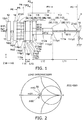
- FIG. 1 is a schematic view showing the configuration of a high-frequency semiconductor amplifier according to this embodiment.
- the high-frequency semiconductor amplifier 1 is composed of an input terminal 10 inputted a fundamental signal S1 including the first frequency band Bw1, an input matching circuit 12 connected to the input terminal 10, a high-frequency semiconductor amplifying element 14 connected to the input matching circuit 12, an output matching circuit 21 connected to the high-frequency semiconductor amplifying element 14, and an output terminal 18 connected to the output matching circuit 21.
- a high-frequency fundamental signal S1 having a first frequency band Bw1 is inputted to the input terminal 10.
- the input end 12p1 of the input matching circuit 12 is connected to the input terminal 10.
- the input end 14p1 of the high-frequency semiconductor amplifying element 14 is connected to the output end 12p2 of the input matching circuit 12.
- the output end 14p2 of the high-frequency semiconductor amplifying element 14 is connected to the input end 21p1 of the output matching circuit 21.
- the output terminal 18 is connected to the output end 21p2 of the output matching circuit 21.
- the input matching circuit 12 is a circuit for matching the power supply impedance with the input impedance of the high-frequency semiconductor amplifying element 14.
- the high-frequency semiconductor amplifying element 14 is an element for amplifying the high-frequency fundamental signal S1.
- An external load Zo is connected in parallel externally seen from the output terminal 18.
- the load impedance m0 of the external load Zo is e.g. 50 ⁇ .
- the DC circuit for supplying voltage to the high-frequency semiconductor amplifying element 14 is not shown.
- the output matching circuit 21 is formed from a microstrip line 111 (ML111), a microstrip line 112 (ML112), a microstrip line 113 (ML113), a microstrip line 114 (ML114), a microstrip line 115 (ML115), and a wire part 116.
- the microstrip line is one example of a transmission line.
- the wire part 116 is formed from e.g. six wires.
- the output matching circuit 21 is a circuit for transforming the load impedance m0 of the external load Zo seen from the output terminal 18 to a desired load impedance md provided to the high-frequency semiconductor amplifying element 14.
- the desired load impedance md is determined by e.g. the load-pull measurement.
- the desired load impedance md is e.g. (1+j1) ⁇ .
- an XYZ orthogonal coordinate system is adopted in this specification. More specifically, in FIG. 1 , the extending direction of the microstrip line 111 is referred to as "X-direction". A direction orthogonal thereto is referred to as "Y-direction". The direction opposite to the "X-direction” is referred to as "-X-direction”. The direction opposite to the "Y-direction” is referred to as "-Y-direction”. The plane including the X-direction and the Y-direction is referred to as X-Y plane. The upward direction perpendicular to this X-Y plane is referred to as "Z-direction".
- the fundamental signal S1 has a first frequency band Bw1.
- the center frequency in the first frequency band Bw1 is referred to as first center frequency f1 or "fundamental frequency f1".
- the wavelength corresponding to the "fundamental frequency f1" is referred to as “fundamental wavelength ⁇ 1".
- the frequency of twice the "fundamental frequency f1” is referred to as “second harmonic frequency f2”.
- the wavelength corresponding to the "second harmonic frequency f2" is referred to as “second harmonic wavelength ⁇ 2”.
- the frequency of three times the "fundamental frequency f1" is referred to as "third harmonic frequency f3".
- the wavelength corresponding to the "third harmonic frequency f3" is referred to as "third harmonic wavelength ⁇ 3".
- microstrip line 111, the microstrip line 112, the microstrip line 113, the microstrip line 114, and the microstrip line 115 schematically show the pattern of microstrip lines.
- the center line splitting the microstrip line 112 in the Y-direction, the center line splitting the microstrip line 113 in the Y-direction, the center line splitting the microstrip line 114 in the Y-direction, and the center line splitting the microstrip line 115 in the Y-direction overlap the center line C splitting the microstrip line 111 in the Y-direction.
- the reference plane P0 is a plane tangent to the X-direction end part of the microstrip line 111 and perpendicular to the X-direction.
- the reference plane P1 is a plane tangent to the X-direction end part of the microstrip line 112 and perpendicular to the X-direction.
- the reference plane P2 is a plane tangent to the X-direction end part of the microstrip line 113 and perpendicular to the X-direction.
- the reference plane P3 is a plane tangent to the X-direction end part of the microstrip line 114 and perpendicular to the X-direction.
- the reference plane P4 is a plane tangent to the X-direction end part of the microstrip line 115 and perpendicular to the X-direction.
- the reference plane P5 is a plane tangent to the -X-direction end part of the microstrip line 115 and perpendicular to the X-direction.
- TABLE 1 is a table illustrating the electrical characteristics and dimensions of the microstrip lines in the high-frequency semiconductor amplifier 1 according to this embodiment.
- the X-direction output end 111p2 of the microstrip line 111 (ML111) is connected to the output terminal 18 (the output end 21p2 of the output matching circuit 21) at the reference plane P0.
- the microstrip line 111 has a line width W11 of 0.310 mm along the Y-direction.
- the microstrip line 111 extends from the reference plane P0 by a line length L11 of 8.690 mm along the -X-direction.
- the input end 111p1 of the microstrip line 111 is connected to the output end 112p2 of the microstrip line 112 at the reference plane P1 to which the microstrip line 111 extends.
- the characteristic impedance Zc11 of the microstrip line 111 is 32.2 ⁇ .
- the relative permittivity ⁇ r11 of the microstrip line 111 is 10.
- the substrate thickness t11 of the microstrip line 111 along the Z-direction is 150 ⁇ m.
- the characteristic impedance Zc11 is lower than the load impedance m0 of the external load Zo.
- the electrical length EL11 of the microstrip line 111 is 85 degrees, being approximately 1/4 times the fundamental wavelength ⁇ 1.
- the electrical length EL11 may be 72 degrees or more and 108 degrees or less at the fundamental frequency f1.
- the microstrip line 112 (ML112) extends from the reference plane P1 by a line length L12 of 7.050 mm along the -X-direction with a line width W12 of 1.810 mm along the Y-direction.
- the input end 113p1 of the microstrip line 113 is connected to the output end 114p2 of the microstrip line 114 at the reference plane P3 to which the microstrip line 112 extends.
- the characteristic impedance Zc12 of the microstrip line 112 is 8.42 ⁇ .
- the relative permittivity ⁇ r12 of the microstrip line 112 is 10.
- the substrate thickness t12 of the microstrip line 112 is 150 ⁇ m.
- the characteristic impedance Zc12 of the microstrip line 112 is lower than the characteristic impedance Zc11.
- the electrical length EL12 of the microstrip line 112 is 75.5 degrees, being approximately 1/4 times the fundamental wavelength ⁇ 1.
- the electrical length EL12 may be 72 degrees or more and 108 degrees or less at the fundamental frequency f1.
- the microstrip line 113 extends from the reference plane P2 by a line length L13 of 0.610 mm along the -X-direction with a line width W13 of 5.010 mm along the Y-direction.
- the input end 113p1 of the microstrip line 113 is connected to the output end 114p2 of the microstrip line 114 at the reference plane P3 to which the microstrip line 113 extends.
- the characteristic impedance Zc13 of the microstrip line 113 is 1.34 ⁇ .
- the relative permittivity ⁇ r13 of the microstrip line 113 is 180.
- the substrate thickness t13 of the microstrip line 113 along the Z-direction is 270 ⁇ m.
- the characteristic impedance Zc13 of the microstrip line 113 is lower than the characteristic impedance Zc12.
- the electrical length EL13 of the microstrip line 113 is 28 degrees, being approximately 1/12 times the fundamental wavelength ⁇ 1.
- the electrical length EL13 may be 24 degrees or more and 36 degrees or less at the fundamental frequency f1.
- the microstrip line 114 (ML114) extends from the reference plane P3 by a line length L14 of 1.38 mm along the -X-direction with a line width W14 of 5.080 mm along the Y-direction.
- the input end 114p1 of the microstrip line 114 is connected to the output end 115p2 of the microstrip line 115 at the reference plane P4 to which the microstrip line 114 extends.
- the characteristic impedance Zc14 of the microstrip line 114 is 5.86 ⁇ .
- the relative permittivity ⁇ r14 of the microstrip line 114 is 10.
- the substrate thickness t14 of the microstrip line 114 along the Z-direction is 280 ⁇ m.
- the characteristic impedance Zc14 of the microstrip line 114 is lower than the characteristic impedance Zc11.
- the characteristic impedance Zc14 is higher than the resistance R of the desired load impedance md provided to the high-frequency semiconductor amplifying element 14.
- the line width W14 along the Y-direction is 0.8 times or more and 1.2 times or less of the line width W13 along the Y-direction.
- the electrical length EL13 of the microstrip line 113 is 15 degrees, being approximately 1/24 times the fundamental wavelength ⁇ 1.
- the electrical length EL14 may be 12 degrees or more and 18 degrees or less at the fundamental frequency f1.
- the microstrip line 115 extends from the reference plane P4 by a line length L15 of 0.49 mm along the -X-direction with a line width W15 of 5.05 mm along the Y-direction.
- the input end 115p1 of the microstrip line 115 is connected to the output end 116p2 of the wire part 116 at the reference plane P5 to which the microstrip line 115 extends.
- the characteristic impedance Zc15 of the microstrip line 115 is 1.38 ⁇ .
- the relative permittivity ⁇ r15 of the microstrip line 115 is 90.
- the substrate thickness t15 of the microstrip line 115 along the Z-direction is 190 ⁇ m.
- the characteristic impedance Zc15 is equal to the resistance R of the desired load impedance md provided to the high-frequency semiconductor amplifying element 14 at the fundamental frequency f1.
- the electrical length EL15 of the microstrip line 115 is 16 degrees, being approximately 1/24 times the fundamental wavelength ⁇ 1.
- the electrical length EL15 may be 12 degrees or more and 18 degrees or less at the fundamental frequency f1.
- the wire part 116 is provided between the microstrip line 115 and the high-frequency semiconductor amplifying element 14.
- the wire part 116 connects the microstrip line 115 and the high-frequency semiconductor amplifying element 14.
- the wire part 116 is formed from e.g. six wires.
- the input end 116p1 of the wire part 116 is connected to the input end 21p1 of the output matching circuit 21.
- the characteristic impedance Zc13 of the microstrip line 113 is 0.8 times or more and 1.2 times or less of the characteristic impedance Zc15 of the microstrip line 115.
- the characteristic impedance Zc14 of the microstrip line 114 is higher than the characteristic impedance Zc13 of the microstrip line 113.
- the relative permittivity ⁇ r13 of the substrate of the microstrip line 113 is 1.6 times or more and 2.4 times or less of the relative permittivity ⁇ r15 of the substrate of the microstrip line 115.
- the relative permittivity ⁇ r14 of the substrate of the microstrip line 114 is 0.08 times or more and 0.12 times or less of the relative permittivity ⁇ r15 of the substrate of the microstrip line 115.
- the relative permittivity ⁇ r14 of the substrate of the microstrip line 114 is equal to the relative permittivity ⁇ r12 of the substrate of the microstrip line 112.
- the relative permittivity ⁇ r12 of the substrate of the microstrip line 112 is 0.08 times or more and 0.12 times or less of the relative permittivity ⁇ r15 of the substrate of the microstrip line 115.
- the relative permittivity ⁇ r15 of the substrate of the microstrip line 115 is higher than the relative permittivity ⁇ r14 of the substrate of the microstrip line 114.
- the substrate thickness t14 along the Z-direction of the microstrip line 114 is 1.6 times or more and 2.4 times or less of the substrate thickness t12 along the Z-direction of the microstrip line 112.
- the substrate thickness t13 along the Z-direction of the microstrip line 113 is 0.8 times or more and 1.2 times or less of the substrate thickness t14 along the Z-direction of the microstrip line 114.
- the line width W14 along the Y-direction of the microstrip line 114 is 0.8 times or more and 1.2 times or less of the line width W15 along the Y-direction of the microstrip line 115.
- the line width W13 along the Y-direction of the microstrip line 113 is 0.8 times or more and 1.2 times or less of the line width W15 along the Y-direction of the microstrip line 115.
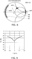
- FIG. 2 is an impedance chart (Smith chart) illustrating the load impedance seen from the reference plane P0 shown in FIG. 1 .
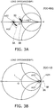
- FIGS. 3A and 3B are impedance charts illustrating the load impedance seen from the reference plane P1 shown in FIG. 1 .
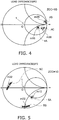
- FIG. 4 is an impedance chart illustrating the load impedance seen from the reference plane P2 shown in FIG. 1 .
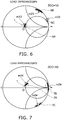
- FIG. 5 is an impedance chart illustrating the load impedance seen from the reference plane P3 shown in FIG. 1 .
- FIG. 6 is an impedance chart illustrating the load impedance seen from the reference plane P4 shown in FIG. 1 .
- FIG. 7 is an impedance chart illustrating the load impedance seen from the reference plane P5 shown in FIG. 1 .
- FIG. 8 is an impedance chart illustrating the load impedance seen from the reference plane P6 shown in FIG. 1 .
- the symbols m10-m15 represent the load impedance at the fundamental frequency f1.
- the symbols m20-m25 represent the load impedance at the second harmonic frequency f2.
- the symbols m30-m35 represent the load impedance at the third harmonic frequency f3.
- This example shows the case where the load impedance m15 at the fundamental frequency f1 seen from the reference plane P5 is transformed to approximately (1+j1) ⁇ .
- the side of the output terminal 18 connected with the external load Zo is seen from the reference plane P0. Then, the load impedance m10 at the fundamental frequency f1, the load impedance m20 at the second harmonic frequency f2, and the load impedance m30 at the third harmonic frequency f3 are located at the center point O near 50 ⁇ .
- the load impedance at the fundamental, second harmonic, and third harmonic frequencies can be determined by measurement and simulation, and indicated on the impedance chart.
- the electrical length of the microstrip line 111 at the fundamental frequency f1 is 85 degrees.
- the electrical length of 85 degrees corresponds to approximately a quarter wavelength.
- the microstrip line 111 operates like a quarter wavelength transformer.
- the characteristic impedance Zc11 of the microstrip line 111 is lower than 50 ⁇ , which is the load impedance m0 of the external load Zo.
- the load impedance m11 at the fundamental frequency f1 seen from the reference plane P1 is transformed to an impedance lower than 50 ⁇ , which is the load impedance m0 of the external load Zo.
- the load impedance in the first frequency band Bw1 is also transformed to a neighborhood portion including the load impedance m11. This portion is indicated as portion 3A in FIGS. 3A and 3B .
- the electrical length EL11 of the microstrip line 111 is approximately a three-quarter wavelength at the third harmonic frequency f3.
- the load impedance m31 at the third harmonic frequency f3 is transformed to the portion 3A.
- the signal having a frequency of three times that of the fundamental signal S1 is referred to as third harmonic signal S3.
- the load impedance for the third harmonic signal S3 having a frequency band is also transformed to the portion 3A having a low impedance.
- the electrical length EL11 of the microstrip line 111 is approximately a two-quarter wavelength at the second harmonic frequency f2.
- the load impedance m21 at the second harmonic frequency f2 remains near 50 ⁇ without substantial change.
- This portion near 50 ⁇ is indicated as portion 3B in FIGS. 3A and 3B .
- the load impedance m21 for the second harmonic is separated from the load impedance m11 for the fundamental and the load impedance m31 for the third harmonic.
- the electrical length of the microstrip line 112 at the fundamental frequency f1 is 75.5 degrees, corresponding to approximately a quarter wavelength.
- the microstrip line 112 operates like a quarter wavelength transformer.
- the characteristic impedance Zc12 of the microstrip line 112 is lower than the load impedance m11 at the fundamental frequency f1 seen from the reference plane P1.
- the load impedance m16 at the fundamental frequency f1 seen from the reference plane P2 is transformed to a lower value than the load impedance m11 at the fundamental frequency f1 seen from the reference plane P1.
- This portion of the transformed impedance is indicated as portion 4A in FIG. 4 .
- the microstrip line 112 corresponds to approximately a three-quarter wavelength at the third harmonic frequency f3.
- the load impedance m36 at the third harmonic frequency f3 is also transformed to a portion 4C having a low impedance.
- the microstrip line 112 corresponds to approximately a two-quarter wavelength at the second harmonic frequency f2.
- the load impedance m26 at the second harmonic frequency f2 remains near 50 ⁇ without substantial change. This portion near 50 ⁇ is indicated as portion 4B in FIG. 4 .
- the characteristic impedance Zc13 of the microstrip line 113 is lower than the characteristic impedance Zc11 of the microstrip line 111.
- the electrical length EL13 at the fundamental frequency f1 is as short as approximately 28 degrees.
- the load impedance m22 at the second harmonic frequency f2 is transformed to a portion 5B different from the portion 5A.
- the electrical length at the fundamental frequency f1 is as short as approximately 28 degrees.
- the electrical length EL13 is less than or equal to a three-quarter wavelength also at the third harmonic frequency f3.
- the load impedance m32 at the third harmonic frequency f3 is transformed to a portion 5C different from the portion 5A and the portion 5B. That is, the load impedances m12, m22, and m32 at the fundamental frequency f1, the second harmonic frequency f2, and the third harmonic frequency f3 are separated.
- the characteristic impedance Zc14 of the microstrip line 114 is higher than the characteristic impedance Zc13 of the microstrip line 113.
- the electrical length EL14 at the fundamental frequency f1 is approximately 15 degrees.
- the microstrip line 114 is added to the microstrip line 113.
- the load impedance m13 at the fundamental frequency f1 seen from the reference plane P4 is transformed to a portion 6A near 1 ⁇ .
- the load impedance m23 at the second harmonic frequency f2 is transformed to a portion 6B.
- the portion 6B is an inductive region near ⁇ ⁇ .
- the load impedance m33 at the third harmonic frequency f3 is transformed to a portion 6C.
- the portion 6C is inductive near ⁇ ⁇ and different from the portion 6B.
- an inductive impedance is indicated in the upper half region of the impedance chart.
- a capacitive impedance is indicated in the lower half region of the impedance chart.
- the characteristic impedance Zc15 of the microstrip line 115 is close to the load impedance m13 at the fundamental frequency f1 seen from the reference plane P4.
- the microstrip line 115 is added to the microstrip line 114.
- the load impedance m14 at the fundamental frequency f1 seen from the reference plane P5 remains near 1 ⁇ without substantial change.
- This portion near 1 ⁇ is indicated as portion 7A in FIG. 7 .
- the load impedance m24 at the second harmonic frequency f2 is transformed to a portion 7B.
- the portion 7B is an inductive region near ⁇ ⁇ .
- the load impedance m34 at the third harmonic frequency f3 is transformed to a portion 7C.
- the portion 7C is a capacitive region. At this stage, the load impedance m34 at the third harmonic frequency f3 is capacitive.
- the wire part 116 is added to the microstrip line 115.
- the load impedance m15 at the fundamental frequency f1 seen from the reference plane P6 is transformed to a portion 8A near (1+j1) ⁇ because of the added inductivity of the wire part 116.
- the load impedance m25 at the second harmonic frequency f2 remains near ⁇ ⁇ .
- This portion near ⁇ ⁇ is indicated as portion 8B in FIG. 8 .
- the load impedance m35 at the third harmonic frequency f3 is transformed to a portion 8C near 0 ⁇ due to resonance between the capacitivity in the aforementioned portion 7C and the inductivity of the wire part 116.
- the amount of capacitivity produced by the addition of the microstrip line 115 may be smaller than the amount of inductivity of the wire part 116.
- the load impedance m35 at the third harmonic frequency f3 is not transformed to approximately 0 ⁇ due to insufficient resonance between capacitivity and inductivity.
- the amount of capacitivity produced by the addition of the microstrip line 115 may be larger than the amount of inductivity of the wire part 116.
- the load impedance m35 at the third harmonic frequency f3 is not transformed to approximately 0 ⁇ due to insufficient resonance between capacitivity and inductivity.
- the electrical length EL15 of the microstrip line 115 needs to be selected so as to achieve resonance between the capacitivity produced by the addition of the microstrip line 115 and the inductivity of the wire part 116.
- the high-frequency semiconductor amplifier 1 has been described with reference to the example in which the load impedance at the fundamental frequency f1 seen from the reference plane P6 is transformed to approximately (1+j1) ⁇ .
- this embodiment is not limited thereto.
- the load impedance may be transformed to a different desired load impedance.
- High power-added efficiency is achieved in the high-frequency semiconductor amplifier by an output matching circuit connected to the output of the high-frequency semiconductor amplifying element.
- the load impedance at the fundamental frequency is matched with a desired impedance.
- the load impedance at even harmonics such as the second harmonic frequency is set to ⁇ ⁇ .
- the load impedance at odd harmonics such as the third harmonic frequency is set to 0 ⁇ .
- Such operation of the high-frequency semiconductor amplifier is referred to as inverse class-F operation.
- the inverse class-F operation of the high-frequency semiconductor amplifier eliminates the even harmonics of voltage and the odd harmonics of current. The voltage and the current both exist only at the fundamental frequency. This realizes high power-added efficiency.
- the load impedance m12 at the fundamental frequency f1 is transformed to the portion 5A shown in FIG. 5 .
- the load impedance m22 at the second harmonic frequency f2 is transformed to the portion 5B shown in FIG. 5 .
- the load impedance m32 at the third harmonic frequency f3 is transformed to the portion 5C shown in FIG. 5 .
- the portions 5A, 5B, and 5C are separate.
- the load impedance m15 at the fundamental frequency f1 seen from the reference plane P6 is easily transformed to the final target of approximately (1+j1) ⁇ .
- the load impedance m25 at the second harmonic frequency f2 is easily transformed to the final target of approximately ⁇ ⁇ .
- the load impedance m35 at the third harmonic frequency f3 is easily transformed to the final target of approximately 0 ⁇ .
- the load impedance m14 at the fundamental frequency f1 remains near 1 ⁇ .
- the load impedance m24 at the second harmonic frequency f2 is transformed to approximately ⁇ ⁇ .
- the load impedance m34 at the third harmonic frequency f3 is transformed to a capacitive region.
- the load impedance m15 at the fundamental frequency f1 is transformed to approximately (1+j1) ⁇ .
- the load impedance m25 at the second harmonic frequency f2 is transformed to approximately ⁇ ⁇ .
- the load impedance m35 at the third harmonic frequency f3 is resonated with the inductivity of the wire part 116 and transformed to approximately 0 ⁇ .
- high power-added efficiency can be achieved by the inverse class-F operation of the high-frequency semiconductor amplifier 1.
- the power-added efficiency can be improved by approximately 5-10%.
- FIG. 9 is a graph illustrating the return loss RL seen from the reference plane P5 shown in FIG. 1 .
- the horizontal axis represents frequency f (GHz).
- the vertical axis represents the return loss RL(dB) for the load impedance m15 provided to the high-frequency semiconductor amplifying element 14.
- the load impedance m15 is e.g. (1+j1) ⁇ .
- the return loss RL at the fundamental frequency f1 can be set to 20 dB or more at frequency f of approximately 2.7-3.1 GHz.
- a high-frequency semiconductor amplifier for performing only the transformation of the load impedance for the fundamental uses a plurality of impedance transformation lines to lower a high impedance to the load impedance provided to the high-frequency semiconductor amplifying element 14.
- the characteristic impedance of the line is made sequentially lower with the decrease of the transformed impedance.
- the line width is also made sequentially wider.
- the high-frequency semiconductor amplifier 1 of this invention controls the load impedance for the second and third harmonics.
- the characteristic impedance Zc14 of the microstrip line 114 needs to be higher than the characteristic impedance Zc13 of the microstrip line 113 and the characteristic impedance Zc15 of the microstrip line 115.
- the line width W13 can be made comparable to the line width W12 and the line width W14.
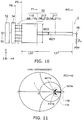
- FIG. 10 is a schematic view showing the configuration of a high-frequency semiconductor amplifier according to this comparative example.
- FIG. 11 is an impedance chart illustrating the load impedance seen from the reference plane P1 shown in FIG. 10 .
- FIG. 12 is an impedance chart illustrating the load impedance seen from the reference plane P2 shown in FIG. 10 .
- FIG. 13 is an impedance chart illustrating the load impedance seen from the reference plane P5 shown in FIG. 10 .
- TABLE 2 is a table illustrating the electrical characteristics and dimensions of the microstrip lines in the first comparative example according to this embodiment.
- the output matching circuit 22 in this comparative example is formed from a microstrip line 211 (ML211), a microstrip line 212 (ML212), and a wire part 115.
- the position of the reference plane P0 is similar to the position in the above first embodiment.
- the load impedance m10 at the fundamental frequency f1 is similar to that of the above first embodiment (see FIG. 2 ).
- the load impedance m20 at the second harmonic frequency f2 is also similar to that of the above first embodiment (see FIG. 2 ).
- the load impedance m30 at the third harmonic frequency f3 is also similar to that of the above first embodiment (see FIG. 2 ).
- the characteristic impedance Zc21 of the microstrip line 211 is 18.8 ⁇ .
- the electrical length EL21 at the fundamental frequency f1 is 90 degrees.
- the relative permittivity ⁇ r21 is 10.
- the substrate thickness t21 is 150 ⁇ m.
- the line width W21 is 0.68 mm.
- the line length L21 is 8.83 mm.
- the characteristic impedance Zc22 of the microstrip line 212 is 2.66 ⁇ .
- the electrical length EL22 at the fundamental frequency f1 is 90 degrees.
- the relative permittivity ⁇ r22 is 40.
- the substrate thickness t22 is 250 ⁇ m.
- the line width W22 is 5.06 mm.
- the line length L22 is 4.14 mm.
- the load impedance m11a at the fundamental frequency f1 and the load impedance m31a at the third harmonic frequency f3 are transformed to a portion 11A having an impedance higher than 1 ⁇ and lower than 50 ⁇ .
- the load impedance m21a at the second harmonic frequency f2 remains near 50 ⁇ . This portion near 50 ⁇ is indicated as portion 11B in FIG. 11 .
- the load impedance m12a at the fundamental frequency f1 and the load impedance m32a at the third harmonic frequency f3 are transformed to a portion 12A having an impedance of approximately 1 ⁇ .
- the load impedance m22a at the second harmonic frequency f2 remains near 50 ⁇ . This portion near 50 ⁇ is indicated as portion 12B in FIG. 12 .
- the load impedance m15a at the fundamental frequency f1 is transformed to a portion 13A near (1+j1) ⁇ because of the added inductivity of the wire part 115.
- the load impedance m25a at the second harmonic frequency f2 is transformed to a portion 13B near ⁇ ⁇ .
- the load impedance m35a at the third harmonic frequency f3 is transformed to a portion 13C.
- the load impedance m25a at the second harmonic frequency f2 is set to approximately ⁇ ⁇ , but the load impedance m35a at the third harmonic frequency f3 is not set to approximately 0 ⁇ .
- FIG. 14 is a schematic view showing the configuration of a high-frequency semiconductor amplifier according to the second comparative example of the first embodiment.
- FIG. 15 is an impedance chart illustrating the load impedance seen from the reference plane P3 shown in FIG. 14 .
- FIG. 16 is an impedance chart illustrating the load impedance seen from the reference plane P5 shown in FIG. 14 .
- TABLE 3 is a table illustrating the electrical characteristics and dimensions of the microstrip lines in the second comparative example according to this embodiment.
- the output matching circuit 23 in the second comparative example of this embodiment is different from the output matching circuit 22 in the above first comparative example in that the microstrip line 313 (ML313) is provided between the microstrip line 212 and the wire part 115.
- the load impedances m10, m11, and m12 at the fundamental frequency f1 are similar to those of the above first comparative example.
- the load impedances m20, m21, and m22 at the second harmonic frequency f2 are similar to those of the above first comparative example.
- the load impedances m30, m31, and m32 at the third harmonic frequency f3 are similar to those of the above first comparative example.
- the characteristic impedance Zc33 of the microstrip line 313 is 1.0 ⁇ .
- the electrical length EL33 at the fundamental frequency f1 is 90 degrees.
- the relative permittivity ⁇ r33 is 90.
- the substrate thickness t33 is 135 ⁇ m.
- the line width W33 is 5.05 mm.
- the line length L33 is 2.71 mm.
- the load impedance m13b at the fundamental frequency f1 remains near 1 ⁇ as in the case seen from the reference plane P2.
- the load impedance m33b at the third harmonic frequency f3 also remains near 1 ⁇ .
- This portion near 1 ⁇ is indicated as portion 15A.
- the phase can be adjusted by adding e.g. a strip line or wire.
- the load impedance m23b at the second harmonic frequency f2 is transformed to a portion 15B near ⁇ ⁇ .
- the impedance is not substantially changed even if the phase is adjusted by adding e.g. a strip line.
- the load impedance m15b at the fundamental frequency f1 is transformed to a portion 16A near (1+j1) ⁇ because of the added inductivity of the wire part 115.
- the load impedance m25b at the second harmonic frequency f2 remains near ⁇ ⁇ without substantial change. This portion near ⁇ ⁇ is indicated as portion 16B in FIG. 16 .
- the load impedance m35b at the third harmonic frequency f3 is transformed to a portion 16C because of the added inductivity of the wire part 115.
- the load impedance m35b at the third harmonic frequency f3 is not set to approximately 0 ⁇ . Thus, it is difficult to cause the high-frequency semiconductor amplifier 3 to perform the inverse class-F operation.
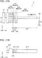
- FIGS. 17A and 17B are schematic views showing the configuration of a high-frequency semiconductor amplifier according to the third comparative example of the first embodiment.
- TABLE 4 is a table illustrating the electrical characteristics and dimensions of the microstrip lines in the third comparative example according to this embodiment.
- ML411 ML412 ML413 ML414 Zc41 ⁇ 44( ⁇ ) 15.90 1.13 4.67 1.00 EL41 ⁇ 44(°) 96.0 26.0 24.0 7.0 ⁇ r41 ⁇ 44 10 90 90 90 t41 ⁇ 44( ⁇ m) 150 135 135 135 W41 ⁇ 44(mm) 0.846 4.440 0.903 5.052 L41 ⁇ 44 (mm) 9.310 0.790 0.780 0.210
- the microstrip line 412 (ML412), the microstrip line 413 (ML413), and the microstrip line 414 (ML414) are formed on a substrate having the same permittivity and the same thickness.
- the line width W43 of the microstrip line 413 is smaller than the line width W42 of the microstrip line 412.
- the line width W43 of the microstrip line 413 is smaller than the line width W44 of the microstrip line 414.
- the line width of the microstrip line 412, the microstrip line 413, and the microstrip line 414 is not constant, but a depression occurs. Thus, unnecessary radio waves are emitted from the microstrip line 412, the microstrip line 413, and the microstrip line 414.
- the embodiment described above can provide a high-frequency semiconductor amplifier for amplifying high-frequency signals at high power-added efficiency.
Landscapes
- Engineering & Computer Science (AREA)
- Power Engineering (AREA)
- Microwave Amplifiers (AREA)
Description
- Embodiments described herein relate generally to a high-frequency semiconductor amplifier.
- An amplifier operating in the high-frequency band of 1 GHz or more has recently been under active development. Such an amplifier is used in e.g. radio communication equipment, mobile communication base stations, and radar devices. This amplifier is required to amplify and transmit signals in the high-frequency band at high power-added efficiency.
- In a microwave semiconductor amplifying element, high efficiency operation called class-F mode can be achieved when the load impedance for the second harmonic seen from the output electrode end of the semiconductor amplifying element is made near-short, and the load impedance for the third harmonic is made near-open. In a known technique, an open-stub that is a tip-open transmission line of 1/8 wavelength of the fundamental is connected to the output electrode end of the semiconductor amplifying element so that the load impedance for the second harmonic seen from the output electrode end of the semiconductor amplifying element is made near-short. An open-stub that is a tip-open transmission line of 1/12 wavelength of the fundamental is connected to the output electrode end of the semiconductor amplifying element through a transmission line of 1/8 wavelength of the fundamental so that the load impedance for the third harmonic is made near-open.
- Furthermore, in a microwave semiconductor amplifying element, high efficiency operation called inverse class-F mode can be achieved when the load impedance for the second harmonic seen from the output electrode end of the semiconductor amplifying element is made near-open, and the load impedance for the third harmonic is made near-short. In a known technique, the impedance for the second harmonic is controlled without affecting the fundamental by a harmonic impedance adjustment line so that the load impedance for the second harmonic is made near-open.
-
US 2014/218105 A1 describes an amplifier including: an amplifying device configured to amplify an input signal; and a matching circuit coupled to the amplifying device, and including an impedance transformer and a parallel resonance circuit coupled to a wiring which spans from the impedance transformer to the amplifying device, wherein a circuit length of the impedance transformer is longer than one fourth of wavelength of an electronic wave having a frequency which is substantially equal to a resonance frequency of the parallel resonance circuit. -
EP 2 637 302 A1 describes a microwave semiconductor amplifier including a semiconductor amplifier element, an input matching circuit and an output matching circuit. The semiconductor amplifying element includes an input electrode and an output electrode and has a capacitive output impedance. The input matching circuit is connected to the input electrode. The output matching circuit includes a bonding wire and a first transmission line. The bonding wire includes first and second end portions. The first end portion is connected to the output electrode. The second end portion is connected to one end portion of the first transmission line. A fundamental impedance and a second harmonic impedance seen toward the external load change toward the one end portion. The second harmonic impedance at the one end portion has an inductive reactance. The output matching circuit matches the capacitive output impedance of the semiconductor amplifying element to the fundamental impedance of the external load.US 2005/231286 discloses an inverse class F amplifier as a peaking amplifier in a Doherty configuration comprising a semiconductor amplifier and a corresponding harmonics tuning and impedance matching network. -
-
FIG. 1 is a schematic view showing the configuration of a high-frequency semiconductor amplifier according to a first embodiment; -
FIG. 2 is an impedance chart (Smith chart) illustrating the load impedance seen from the reference plane P0 shown inFIG. 1 ; -
FIGS. 3A and 3B are impedance charts illustrating the load impedance seen from the reference plane P1 shown inFIG. 1 ; -
FIG. 4 is an impedance chart illustrating the load impedance seen from the reference plane P2 shown inFIG. 1 ; -
FIG. 5 is an impedance chart illustrating the load impedance seen from the reference plane P3 shown inFIG. 1 ; -
FIG. 6 is an impedance chart illustrating the load impedance seen from the reference plane P4 shown inFIG. 1 ; -
FIG. 7 is an impedance chart illustrating the load impedance seen from the reference plane P5 shown inFIG. 1 ; -
FIG. 8 is an impedance chart illustrating the load impedance seen from the reference plane P6 shown inFIG. 1 ; -
FIG. 9 is a graph illustrating the return loss RL seen from the reference plane P6 shown inFIG. 1 ; -
FIG. 10 is a schematic view showing the configuration of a high-frequency semiconductor amplifier according to a first comparative example of the first embodiment; -
FIG. 11 is an impedance chart illustrating the load impedance seen from the reference plane P1 shown inFIG. 10 ; -
FIG. 12 is an impedance chart illustrating the load impedance seen from the reference plane P2 shown inFIG. 10 ; -
FIG. 13 is an impedance chart illustrating the load impedance seen from the reference plane P6 shown inFIG. 10 ; -
FIG. 14 is a schematic view showing the configuration of a high-frequency semiconductor amplifier according to a second comparative example of the first embodiment; -
FIG. 15 is an impedance chart illustrating the load impedance seen from the reference plane P3 shown inFIG. 14 ; -
FIG. 16 is an impedance chart illustrating the load impedance seen from the reference plane P5 shown inFIG. 14 ; and -
FIGS. 17A and 17B are schematic views showing the configuration of a high-frequency semiconductor amplifier according to a third comparative example of the first embodiment. - In accordance with the invention, a high frequency semiconductor amplifier is defined by the features of
claim 1. - Further embodiments are provided by the dependent claims.
- Embodiments of the invention will now be described with reference to the drawings.
- The drawings are schematic or conceptual. The relationship between the thickness and the width of each portion, and the size ratio between the portions, for instance, are not necessarily identical to those in reality. Furthermore, the same portion may be shown with different dimensions or ratios depending on the figures.
- In this specification and the drawings, components similar to those described previously with reference to earlier figures are labeled with like reference numerals, and the detailed description thereof is omitted appropriately.
-
FIG. 1 is a schematic view showing the configuration of a high-frequency semiconductor amplifier according to this embodiment. - First, the configuration of the high-frequency semiconductor amplifier according to this embodiment is described.
- As shown in
FIG. 1 , the high-frequency semiconductor amplifier 1 is composed of aninput terminal 10 inputted a fundamental signal S1 including the first frequency band Bw1, aninput matching circuit 12 connected to theinput terminal 10, a high-frequencysemiconductor amplifying element 14 connected to theinput matching circuit 12, anoutput matching circuit 21 connected to the high-frequencysemiconductor amplifying element 14, and anoutput terminal 18 connected to theoutput matching circuit 21. A high-frequency fundamental signal S1 having a first frequency band Bw1 is inputted to theinput terminal 10. The input end 12p1 of theinput matching circuit 12 is connected to theinput terminal 10. The input end 14p1 of the high-frequencysemiconductor amplifying element 14 is connected to the output end 12p2 of theinput matching circuit 12. The output end 14p2 of the high-frequencysemiconductor amplifying element 14 is connected to the input end 21p1 of theoutput matching circuit 21. Theoutput terminal 18 is connected to the output end 21p2 of theoutput matching circuit 21. - The
input matching circuit 12 is a circuit for matching the power supply impedance with the input impedance of the high-frequencysemiconductor amplifying element 14. The high-frequencysemiconductor amplifying element 14 is an element for amplifying the high-frequency fundamental signal S1. An external load Zo is connected in parallel externally seen from theoutput terminal 18. The load impedance m0 of the external load Zo is e.g. 50 Ω. - The DC circuit for supplying voltage to the high-frequency
semiconductor amplifying element 14 is not shown. - The
output matching circuit 21 is formed from a microstrip line 111 (ML111), a microstrip line 112 (ML112), a microstrip line 113 (ML113), a microstrip line 114 (ML114), a microstrip line 115 (ML115), and awire part 116. The microstrip line is one example of a transmission line. Thewire part 116 is formed from e.g. six wires. Theoutput matching circuit 21 is a circuit for transforming the load impedance m0 of the external load Zo seen from theoutput terminal 18 to a desired load impedance md provided to the high-frequencysemiconductor amplifying element 14. The desired load impedance md is determined by e.g. the load-pull measurement. The desired load impedance md is e.g. (1+j1) Ω. - In the following, for convenience of description, an XYZ orthogonal coordinate system is adopted in this specification. More specifically, in
FIG. 1 , the extending direction of themicrostrip line 111 is referred to as "X-direction". A direction orthogonal thereto is referred to as "Y-direction". The direction opposite to the "X-direction" is referred to as "-X-direction". The direction opposite to the "Y-direction" is referred to as "-Y-direction". The plane including the X-direction and the Y-direction is referred to as X-Y plane. The upward direction perpendicular to this X-Y plane is referred to as "Z-direction". - In this specification, the fundamental signal S1 has a first frequency band Bw1. The center frequency in the first frequency band Bw1 is referred to as first center frequency f1 or "fundamental frequency f1". The wavelength corresponding to the "fundamental frequency f1" is referred to as "fundamental wavelength λ1". The frequency of twice the "fundamental frequency f1" is referred to as "second harmonic frequency f2". The wavelength corresponding to the "second harmonic frequency f2" is referred to as "second harmonic wavelength λ2". The frequency of three times the "fundamental frequency f1" is referred to as "third harmonic frequency f3". The wavelength corresponding to the "third harmonic frequency f3" is referred to as "third harmonic wavelength λ3".
- The
microstrip line 111, themicrostrip line 112, themicrostrip line 113, themicrostrip line 114, and themicrostrip line 115 schematically show the pattern of microstrip lines. - The center line splitting the
microstrip line 112 in the Y-direction, the center line splitting themicrostrip line 113 in the Y-direction, the center line splitting themicrostrip line 114 in the Y-direction, and the center line splitting themicrostrip line 115 in the Y-direction overlap the center line C splitting themicrostrip line 111 in the Y-direction. - The reference plane P0 is a plane tangent to the X-direction end part of the
microstrip line 111 and perpendicular to the X-direction. The reference plane P1 is a plane tangent to the X-direction end part of themicrostrip line 112 and perpendicular to the X-direction. The reference plane P2 is a plane tangent to the X-direction end part of themicrostrip line 113 and perpendicular to the X-direction. The reference plane P3 is a plane tangent to the X-direction end part of themicrostrip line 114 and perpendicular to the X-direction. The reference plane P4 is a plane tangent to the X-direction end part of themicrostrip line 115 and perpendicular to the X-direction. The reference plane P5 is a plane tangent to the -X-direction end part of themicrostrip line 115 and perpendicular to the X-direction. - TABLE 1 is a table illustrating the electrical characteristics and dimensions of the microstrip lines in the high-
frequency semiconductor amplifier 1 according to this embodiment.[TABLE 1] ML111 ML112 ML113 ML114 ML115 Zc11-15(Ω) 32.20 8.42 1.34 5.86 1.38 EL11-15(°) 85.0 75.5 28.0 15.0 16.0 εr11-15 10 10 180 10 90 t11-15(µm) 150 150 270 280 190 W11-15(mm) 0.310 1.810 5.010 5.080 5.050 L11-15(mm) 8.690 7.050 0.610 1.380 0.490 - The X-direction output end 111p2 of the microstrip line 111 (ML111) is connected to the output terminal 18 (the output end 21p2 of the output matching circuit 21) at the reference plane P0. The
microstrip line 111 has a line width W11 of 0.310 mm along the Y-direction. Themicrostrip line 111 extends from the reference plane P0 by a line length L11 of 8.690 mm along the -X-direction. The input end 111p1 of themicrostrip line 111 is connected to the output end 112p2 of themicrostrip line 112 at the reference plane P1 to which themicrostrip line 111 extends. The characteristic impedance Zc11 of themicrostrip line 111 is 32.2 Ω. The relative permittivity εr11 of themicrostrip line 111 is 10. The substrate thickness t11 of themicrostrip line 111 along the Z-direction is 150 µm. The characteristic impedance Zc11 is lower than the load impedance m0 of the external load Zo. At the fundamental frequency (first center frequency) f1, the electrical length EL11 of themicrostrip line 111 is 85 degrees, being approximately 1/4 times the fundamental wavelength λ1. The electrical length EL11 may be 72 degrees or more and 108 degrees or less at the fundamental frequency f1. - The microstrip line 112 (ML112) extends from the reference plane P1 by a line length L12 of 7.050 mm along the -X-direction with a line width W12 of 1.810 mm along the Y-direction. The input end 113p1 of the
microstrip line 113 is connected to the output end 114p2 of themicrostrip line 114 at the reference plane P3 to which themicrostrip line 112 extends. The characteristic impedance Zc12 of themicrostrip line 112 is 8.42 Ω. The relative permittivity εr12 of themicrostrip line 112 is 10. The substrate thickness t12 of themicrostrip line 112 is 150 µm. The characteristic impedance Zc12 of themicrostrip line 112 is lower than the characteristic impedance Zc11. At the fundamental frequency f1, the electrical length EL12 of themicrostrip line 112 is 75.5 degrees, being approximately 1/4 times the fundamental wavelength λ1. The electrical length EL12 may be 72 degrees or more and 108 degrees or less at the fundamental frequency f1. - The microstrip line 113 (ML113) extends from the reference plane P2 by a line length L13 of 0.610 mm along the -X-direction with a line width W13 of 5.010 mm along the Y-direction. The input end 113p1 of the
microstrip line 113 is connected to the output end 114p2 of themicrostrip line 114 at the reference plane P3 to which themicrostrip line 113 extends. The characteristic impedance Zc13 of themicrostrip line 113 is 1.34 Ω. The relative permittivity εr13 of themicrostrip line 113 is 180. The substrate thickness t13 of themicrostrip line 113 along the Z-direction is 270 µm. The characteristic impedance Zc13 of themicrostrip line 113 is lower than the characteristic impedance Zc12. At the fundamental frequency f1, the electrical length EL13 of themicrostrip line 113 is 28 degrees, being approximately 1/12 times the fundamental wavelength λ1. The electrical length EL13 may be 24 degrees or more and 36 degrees or less at the fundamental frequency f1. - The microstrip line 114 (ML114) extends from the reference plane P3 by a line length L14 of 1.38 mm along the -X-direction with a line width W14 of 5.080 mm along the Y-direction. The input end 114p1 of the
microstrip line 114 is connected to the output end 115p2 of themicrostrip line 115 at the reference plane P4 to which themicrostrip line 114 extends. The characteristic impedance Zc14 of themicrostrip line 114 is 5.86 Ω. The relative permittivity εr14 of themicrostrip line 114 is 10. The substrate thickness t14 of themicrostrip line 114 along the Z-direction is 280 µm. The characteristic impedance Zc14 of themicrostrip line 114 is lower than the characteristic impedance Zc11. The characteristic impedance Zc14 is higher than the resistance R of the desired load impedance md provided to the high-frequencysemiconductor amplifying element 14. The line width W14 along the Y-direction is 0.8 times or more and 1.2 times or less of the line width W13 along the Y-direction. At the fundamental frequency f1, the electrical length EL13 of themicrostrip line 113 is 15 degrees, being approximately 1/24 times the fundamental wavelength λ1. The electrical length EL14 may be 12 degrees or more and 18 degrees or less at the fundamental frequency f1. - The microstrip line 115 (ML115) extends from the reference plane P4 by a line length L15 of 0.49 mm along the -X-direction with a line width W15 of 5.05 mm along the Y-direction. The input end 115p1 of the
microstrip line 115 is connected to the output end 116p2 of thewire part 116 at the reference plane P5 to which themicrostrip line 115 extends. The characteristic impedance Zc15 of themicrostrip line 115 is 1.38 Ω. The relative permittivity εr15 of themicrostrip line 115 is 90. The substrate thickness t15 of themicrostrip line 115 along the Z-direction is 190 µm. The characteristic impedance Zc15 is equal to the resistance R of the desired load impedance md provided to the high-frequencysemiconductor amplifying element 14 at the fundamental frequency f1. The electrical length EL15 of themicrostrip line 115 is 16 degrees, being approximately 1/24 times the fundamental wavelength λ1. The electrical length EL15 may be 12 degrees or more and 18 degrees or less at the fundamental frequency f1. - The
wire part 116 is provided between themicrostrip line 115 and the high-frequencysemiconductor amplifying element 14. Thewire part 116 connects themicrostrip line 115 and the high-frequencysemiconductor amplifying element 14. Thewire part 116 is formed from e.g. six wires. - The input end 116p1 of the
wire part 116 is connected to the input end 21p1 of theoutput matching circuit 21. - The characteristic impedance Zc13 of the
microstrip line 113 is 0.8 times or more and 1.2 times or less of the characteristic impedance Zc15 of themicrostrip line 115. The characteristic impedance Zc14 of themicrostrip line 114 is higher than the characteristic impedance Zc13 of themicrostrip line 113. - The relative permittivity εr13 of the substrate of the
microstrip line 113 is 1.6 times or more and 2.4 times or less of the relative permittivity εr15 of the substrate of themicrostrip line 115. The relative permittivity εr14 of the substrate of themicrostrip line 114 is 0.08 times or more and 0.12 times or less of the relative permittivity εr15 of the substrate of themicrostrip line 115. The relative permittivity εr14 of the substrate of themicrostrip line 114 is equal to the relative permittivity εr12 of the substrate of themicrostrip line 112. The relative permittivity εr12 of the substrate of themicrostrip line 112 is 0.08 times or more and 0.12 times or less of the relative permittivity εr15 of the substrate of themicrostrip line 115. The relative permittivity εr15 of the substrate of themicrostrip line 115 is higher than the relative permittivity εr14 of the substrate of themicrostrip line 114. - The substrate thickness t14 along the Z-direction of the
microstrip line 114 is 1.6 times or more and 2.4 times or less of the substrate thickness t12 along the Z-direction of themicrostrip line 112. The substrate thickness t13 along the Z-direction of themicrostrip line 113 is 0.8 times or more and 1.2 times or less of the substrate thickness t14 along the Z-direction of themicrostrip line 114. - The line width W14 along the Y-direction of the
microstrip line 114 is 0.8 times or more and 1.2 times or less of the line width W15 along the Y-direction of themicrostrip line 115. The line width W13 along the Y-direction of themicrostrip line 113 is 0.8 times or more and 1.2 times or less of the line width W15 along the Y-direction of themicrostrip line 115. - Next, the operation of the high-
frequency semiconductor amplifier 1 according to this embodiment is described. -
FIG. 2 is an impedance chart (Smith chart) illustrating the load impedance seen from the reference plane P0 shown inFIG. 1 . -
FIGS. 3A and 3B are impedance charts illustrating the load impedance seen from the reference plane P1 shown inFIG. 1 . -
FIG. 4 is an impedance chart illustrating the load impedance seen from the reference plane P2 shown inFIG. 1 . -
FIG. 5 is an impedance chart illustrating the load impedance seen from the reference plane P3 shown inFIG. 1 . -
FIG. 6 is an impedance chart illustrating the load impedance seen from the reference plane P4 shown inFIG. 1 . -
FIG. 7 is an impedance chart illustrating the load impedance seen from the reference plane P5 shown inFIG. 1 . -
FIG. 8 is an impedance chart illustrating the load impedance seen from the reference plane P6 shown inFIG. 1 . - The impedance chart of
FIG. 2 is normalized so that the center point O represents 50 Ω (characteristic impedance ZCC = 50 Ω). - The impedance chart of
FIG. 3A is normalized so that the center point O represents 50 Ω (ZCC = 50 Ω). The impedance chart ofFIG. 3B is normalized so that the center point O represents 1 Ω (ZCC = 1 Ω). - The impedance charts of
FIGS. 4 to 8 are normalized so that the center point O represents 1 Ω (ZCC = 1 Ω). - In
FIGS. 2 to 8 , the symbols m10-m15 represent the load impedance at the fundamental frequency f1. The symbols m20-m25 represent the load impedance at the second harmonic frequency f2. The symbols m30-m35 represent the load impedance at the third harmonic frequency f3. - This example shows the case where the load impedance m15 at the fundamental frequency f1 seen from the reference plane P5 is transformed to approximately (1+j1) Ω.
- As shown in
FIG. 2 , the side of theoutput terminal 18 connected with the external load Zo is seen from the reference plane P0. Then, the load impedance m10 at the fundamental frequency f1, the load impedance m20 at the second harmonic frequency f2, and the load impedance m30 at the third harmonic frequency f3 are located at the center point O near 50 Ω. - The load impedance at the fundamental, second harmonic, and third harmonic frequencies can be determined by measurement and simulation, and indicated on the impedance chart.
- As shown in TABLE 1, the electrical length of the
microstrip line 111 at the fundamental frequency f1 is 85 degrees. The electrical length of 85 degrees corresponds to approximately a quarter wavelength. Thus, themicrostrip line 111 operates like a quarter wavelength transformer. - The characteristic impedance Zc11 of the
microstrip line 111 is lower than 50 Ω, which is the load impedance m0 of the external load Zo. Thus, as shown inFIGS. 3A and 3B , the load impedance m11 at the fundamental frequency f1 seen from the reference plane P1 is transformed to an impedance lower than 50 Ω, which is the load impedance m0 of the external load Zo. The load impedance in the first frequency band Bw1 is also transformed to a neighborhood portion including the load impedance m11. This portion is indicated asportion 3A inFIGS. 3A and 3B . - The electrical length EL11 of the
microstrip line 111 is approximately a three-quarter wavelength at the third harmonic frequency f3. Thus, the load impedance m31 at the third harmonic frequency f3 is transformed to theportion 3A. The signal having a frequency of three times that of the fundamental signal S1 is referred to as third harmonic signal S3. The load impedance for the third harmonic signal S3 having a frequency band is also transformed to theportion 3A having a low impedance. - The electrical length EL11 of the
microstrip line 111 is approximately a two-quarter wavelength at the second harmonic frequency f2. Thus, the load impedance m21 at the second harmonic frequency f2 remains near 50 Ω without substantial change. This portion near 50 Ω is indicated asportion 3B inFIGS. 3A and 3B . At this stage, only the load impedance m21 for the second harmonic is separated from the load impedance m11 for the fundamental and the load impedance m31 for the third harmonic. - As shown in TABLE 1, the electrical length of the
microstrip line 112 at the fundamental frequency f1 is 75.5 degrees, corresponding to approximately a quarter wavelength. Thus, themicrostrip line 112 operates like a quarter wavelength transformer. - The characteristic impedance Zc12 of the
microstrip line 112 is lower than the load impedance m11 at the fundamental frequency f1 seen from the reference plane P1. Thus, as shown inFIG. 4 , the load impedance m16 at the fundamental frequency f1 seen from the reference plane P2 is transformed to a lower value than the load impedance m11 at the fundamental frequency f1 seen from the reference plane P1. This portion of the transformed impedance is indicated asportion 4A inFIG. 4 . Themicrostrip line 112 corresponds to approximately a three-quarter wavelength at the third harmonic frequency f3. Thus, the load impedance m36 at the third harmonic frequency f3 is also transformed to aportion 4C having a low impedance. Themicrostrip line 112 corresponds to approximately a two-quarter wavelength at the second harmonic frequency f2. The load impedance m26 at the second harmonic frequency f2 remains near 50 Ω without substantial change. This portion near 50 Ω is indicated asportion 4B inFIG. 4 . - The characteristic impedance Zc13 of the
microstrip line 113 is lower than the characteristic impedance Zc11 of themicrostrip line 111. The electrical length EL13 at the fundamental frequency f1 is as short as approximately 28 degrees. Thus, as shown inFIG. 5 , the load impedance m12 at the fundamental frequency f1 seen from the reference plane P3 is transformed to aportion 5A on the resistance of R = 1 Ω. The resistance of R = 1 Ω is the same value as the resistance component of the desired load impedance md provided to the high-frequencysemiconductor amplifying element 14. The load impedance m22 at the second harmonic frequency f2 is transformed to aportion 5B different from theportion 5A. The electrical length at the fundamental frequency f1 is as short as approximately 28 degrees. Thus, the electrical length EL13 is less than or equal to a three-quarter wavelength also at the third harmonic frequency f3. Accordingly, the load impedance m32 at the third harmonic frequency f3 is transformed to aportion 5C different from theportion 5A and theportion 5B. That is, the load impedances m12, m22, and m32 at the fundamental frequency f1, the second harmonic frequency f2, and the third harmonic frequency f3 are separated. - The characteristic impedance Zc14 of the
microstrip line 114 is higher than the characteristic impedance Zc13 of themicrostrip line 113. The electrical length EL14 at the fundamental frequency f1 is approximately 15 degrees. Themicrostrip line 114 is added to themicrostrip line 113. Thus, as shown inFIG. 6 , the load impedance m13 at the fundamental frequency f1 seen from the reference plane P4 is transformed to aportion 6A near 1 Ω. The load impedance m23 at the second harmonic frequency f2 is transformed to aportion 6B. Theportion 6B is an inductive region near ∞ Ω. The load impedance m33 at the third harmonic frequency f3 is transformed to aportion 6C. Theportion 6C is inductive near ∞ Ω and different from theportion 6B. - In the impedance chart of
FIG. 6 , an inductive impedance is indicated in the upper half region of the impedance chart. A capacitive impedance is indicated in the lower half region of the impedance chart. - The characteristic impedance Zc15 of the
microstrip line 115 is close to the load impedance m13 at the fundamental frequency f1 seen from the reference plane P4. Themicrostrip line 115 is added to themicrostrip line 114. Thus, as shown inFIG. 7 , the load impedance m14 at the fundamental frequency f1 seen from the reference plane P5 remains near 1 Ω without substantial change. This portion near 1 Ω is indicated asportion 7A inFIG. 7 . The load impedance m24 at the second harmonic frequency f2 is transformed to aportion 7B. Theportion 7B is an inductive region near ∞ Ω. The load impedance m34 at the third harmonic frequency f3 is transformed to aportion 7C. Theportion 7C is a capacitive region. At this stage, the load impedance m34 at the third harmonic frequency f3 is capacitive. - The
wire part 116 is added to themicrostrip line 115. Thus, as shown inFIG. 8 , the load impedance m15 at the fundamental frequency f1 seen from the reference plane P6 is transformed to aportion 8A near (1+j1) Ω because of the added inductivity of thewire part 116. The load impedance m25 at the second harmonic frequency f2 remains near ∞ Ω. This portion near ∞ Ω is indicated asportion 8B inFIG. 8 . The load impedance m35 at the third harmonic frequency f3 is transformed to aportion 8C near 0 Ω due to resonance between the capacitivity in theaforementioned portion 7C and the inductivity of thewire part 116. - The amount of capacitivity produced by the addition of the
microstrip line 115 may be smaller than the amount of inductivity of thewire part 116. In this case, the load impedance m35 at the third harmonic frequency f3 is not transformed to approximately 0 Ω due to insufficient resonance between capacitivity and inductivity. The amount of capacitivity produced by the addition of themicrostrip line 115 may be larger than the amount of inductivity of thewire part 116. Also in this case, the load impedance m35 at the third harmonic frequency f3 is not transformed to approximately 0 Ω due to insufficient resonance between capacitivity and inductivity. - Thus, the electrical length EL15 of the
microstrip line 115 needs to be selected so as to achieve resonance between the capacitivity produced by the addition of themicrostrip line 115 and the inductivity of thewire part 116. - The high-
frequency semiconductor amplifier 1 according to this embodiment has been described with reference to the example in which the load impedance at the fundamental frequency f1 seen from the reference plane P6 is transformed to approximately (1+j1) Ω. However, this embodiment is not limited thereto. The load impedance may be transformed to a different desired load impedance. - Next, the effect of the high-
frequency semiconductor amplifier 1 according to this embodiment is described. - High power-added efficiency is achieved in the high-frequency semiconductor amplifier by an output matching circuit connected to the output of the high-frequency semiconductor amplifying element. Thus, the load impedance at the fundamental frequency is matched with a desired impedance. The load impedance at even harmonics such as the second harmonic frequency is set to ∞ Ω. The load impedance at odd harmonics such as the third harmonic frequency is set to 0 Ω. Such operation of the high-frequency semiconductor amplifier is referred to as inverse class-F operation. The inverse class-F operation of the high-frequency semiconductor amplifier eliminates the even harmonics of voltage and the odd harmonics of current. The voltage and the current both exist only at the fundamental frequency. This realizes high power-added efficiency.
- In the high-
frequency semiconductor amplifier 1 according to this embodiment, by themicrostrip line 113, the load impedance m12 at the fundamental frequency f1 is transformed to theportion 5A shown inFIG. 5 . The load impedance m22 at the second harmonic frequency f2 is transformed to theportion 5B shown inFIG. 5 . The load impedance m32 at the third harmonic frequency f3 is transformed to theportion 5C shown inFIG. 5 . Theportions - By the
microstrip line 115, the load impedance m14 at the fundamental frequency f1 remains near 1 Ω. However, the load impedance m24 at the second harmonic frequency f2 is transformed to approximately ∞ Ω. The load impedance m34 at the third harmonic frequency f3 is transformed to a capacitive region. - By the
wire part 116, the load impedance m15 at the fundamental frequency f1 is transformed to approximately (1+j1) Ω. The load impedance m25 at the second harmonic frequency f2 is transformed to approximately ∞ Ω. The load impedance m35 at the third harmonic frequency f3 is resonated with the inductivity of thewire part 116 and transformed to approximately 0 Ω. As a result, high power-added efficiency can be achieved by the inverse class-F operation of the high-frequency semiconductor amplifier 1. The power-added efficiency can be improved by approximately 5-10%. -
FIG. 9 is a graph illustrating the return loss RL seen from the reference plane P5 shown inFIG. 1 . InFIG. 9 , the horizontal axis represents frequency f (GHz). The vertical axis represents the return loss RL(dB) for the load impedance m15 provided to the high-frequencysemiconductor amplifying element 14. The load impedance m15 is e.g. (1+j1) Ω. - As shown in
FIG. 9 , the return loss RL at the fundamental frequency f1 can be set to 20 dB or more at frequency f of approximately 2.7-3.1 GHz. - A high-frequency semiconductor amplifier for performing only the transformation of the load impedance for the fundamental uses a plurality of impedance transformation lines to lower a high impedance to the load impedance provided to the high-frequency
semiconductor amplifying element 14. Thus, the characteristic impedance of the line is made sequentially lower with the decrease of the transformed impedance. As a result, the line width is also made sequentially wider. However, the high-frequency semiconductor amplifier 1 of this invention controls the load impedance for the second and third harmonics. Thus, the characteristic impedance Zc14 of themicrostrip line 114 needs to be higher than the characteristic impedance Zc13 of themicrostrip line 113 and the characteristic impedance Zc15 of themicrostrip line 115. Accordingly, as in TABLE 4 shown in the third comparative example described later, if themicrostrip line 412, themicrostrip line 413, and themicrostrip line 414 are formed on a substrate having the same permittivity and the same thickness, then the line width is not made sequentially wider, but a depression occurs as shown inFIG. 17A . Thus, while the substrate thickness and the relative permittivity of the substrate of themicrostrip line 113 are selected from among commercially available ones, the substrate thickness is optimized. Accordingly, the line width W13 can be made comparable to the line width W12 and the line width W14. As a result, discontinuity in the pattern of microstrip lines is eliminated in themicrostrip lines - Next, a first comparative example of the first embodiment is described.
-
FIG. 10 is a schematic view showing the configuration of a high-frequency semiconductor amplifier according to this comparative example. -
FIG. 11 is an impedance chart illustrating the load impedance seen from the reference plane P1 shown inFIG. 10 . -
FIG. 12 is an impedance chart illustrating the load impedance seen from the reference plane P2 shown inFIG. 10 . -
FIG. 13 is an impedance chart illustrating the load impedance seen from the reference plane P5 shown inFIG. 10 . - The impedance charts of
FIGS. 11 to 13 are normalized so that the center point O represents 1 Ω (ZCC = 1 Ω). - TABLE 2 is a table illustrating the electrical characteristics and dimensions of the microstrip lines in the first comparative example according to this embodiment.
[TABLE 2] ML211 ML212 Zc21, 22(Ω) 18.80 2.66 EL21, 22(°) 90.0 90.0 ε r21, 22 10 40 t21, 22(µm) 150 250 W21, 22(mm) 0.680 5.060 L21, 22(mm) 8.830 4.140 - As shown in
FIG. 10 , theoutput matching circuit 22 in this comparative example is formed from a microstrip line 211 (ML211), a microstrip line 212 (ML212), and awire part 115. The position of the reference plane P0 is similar to the position in the above first embodiment. Thus, when theoutput terminal 18 side is seen from the reference plane P0, the load impedance m10 at the fundamental frequency f1 is similar to that of the above first embodiment (seeFIG. 2 ). The load impedance m20 at the second harmonic frequency f2 is also similar to that of the above first embodiment (seeFIG. 2 ). The load impedance m30 at the third harmonic frequency f3 is also similar to that of the above first embodiment (seeFIG. 2 ). - The characteristic impedance Zc21 of the
microstrip line 211 is 18.8 Ω. The electrical length EL21 at the fundamental frequency f1 is 90 degrees. The relative permittivity εr21 is 10. The substrate thickness t21 is 150 µm. The line width W21 is 0.68 mm. The line length L21 is 8.83 mm. The characteristic impedance Zc22 of themicrostrip line 212 is 2.66 Ω. The electrical length EL22 at the fundamental frequency f1 is 90 degrees. The relative permittivity εr22 is 40. The substrate thickness t22 is 250 µm. The line width W22 is 5.06 mm. The line length L22 is 4.14 mm. - As shown in
FIG. 11 , when theoutput terminal 18 side is seen from the reference plane P1, the load impedance m11a at the fundamental frequency f1 and the load impedance m31a at the third harmonic frequency f3 are transformed to aportion 11A having an impedance higher than 1 Ω and lower than 50 Ω. The load impedance m21a at the second harmonic frequency f2 remains near 50 Ω. This portion near 50 Ω is indicated asportion 11B inFIG. 11 . - As shown in
FIG. 12 , when theoutput terminal 18 side is seen from the reference plane P2, the load impedance m12a at the fundamental frequency f1 and the load impedance m32a at the third harmonic frequency f3 are transformed to aportion 12A having an impedance of approximately 1 Ω. The load impedance m22a at the second harmonic frequency f2 remains near 50 Ω. This portion near 50 Ω is indicated asportion 12B inFIG. 12 . - As shown in
FIG. 13 , when theoutput terminal 18 side is seen from the reference plane P5, the load impedance m15a at the fundamental frequency f1 is transformed to aportion 13A near (1+j1) Ω because of the added inductivity of thewire part 115. The load impedance m25a at the second harmonic frequency f2 is transformed to aportion 13B near ∞ Ω. The load impedance m35a at the third harmonic frequency f3 is transformed to aportion 13C. The load impedance m25a at the second harmonic frequency f2 is set to approximately ∞ Ω, but the load impedance m35a at the third harmonic frequency f3 is not set to approximately 0 Ω. Thus, it is difficult to cause the high-frequency semiconductor amplifier 2 to perform the inverse class-F operation. - Next, a second comparative example of the first embodiment is described.
-
FIG. 14 is a schematic view showing the configuration of a high-frequency semiconductor amplifier according to the second comparative example of the first embodiment. -
FIG. 15 is an impedance chart illustrating the load impedance seen from the reference plane P3 shown inFIG. 14 . -
FIG. 16 is an impedance chart illustrating the load impedance seen from the reference plane P5 shown inFIG. 14 . - The impedance charts of
FIGS. 15 and16 are normalized so that the center point O represents 1 Ω (ZCC = 1 Ω). - TABLE 3 is a table illustrating the electrical characteristics and dimensions of the microstrip lines in the second comparative example according to this embodiment.
[TABLE 3] ML211 ML212 ML313 Zc21, 22, 33(Ω) 18.80 2.66 1.00 EL21, 22, 33(°) 90.0 90.0 90.0 ε r21, 22, 33 10 40 90 t21, 22, 33(µm) 150 250 135 W21, 22, 33(mm) 0.680 5.060 5.050 L21, 22, 33(mm) 8.830 4.140 2.710 - As shown in
FIG. 14 , theoutput matching circuit 23 in the second comparative example of this embodiment is different from theoutput matching circuit 22 in the above first comparative example in that the microstrip line 313 (ML313) is provided between themicrostrip line 212 and thewire part 115. Thus, when theoutput terminal 18 side is seen from the reference planes P0, P1, and P2, the load impedances m10, m11, and m12 at the fundamental frequency f1 are similar to those of the above first comparative example. When theoutput terminal 18 side is seen from the reference planes P0, P1, and P2, the load impedances m20, m21, and m22 at the second harmonic frequency f2 are similar to those of the above first comparative example. When theoutput terminal 18 side is seen from the reference planes P0, P1, and P2, the load impedances m30, m31, and m32 at the third harmonic frequency f3 are similar to those of the above first comparative example. The characteristic impedance Zc33 of themicrostrip line 313 is 1.0 Ω. The electrical length EL33 at the fundamental frequency f1 is 90 degrees. The relative permittivity εr33 is 90. The substrate thickness t33 is 135 µm. The line width W33 is 5.05 mm. The line length L33 is 2.71 mm. - As shown in
FIG. 15 , when theoutput terminal 18 side is seen from the reference plane P3, the load impedance m13b at the fundamental frequency f1 remains near 1 Ω as in the case seen from the reference plane P2. The load impedance m33b at the third harmonic frequency f3 also remains near 1 Ω. This portion near 1 Ω is indicated asportion 15A. In the case where the load impedance is located in theportion 15A, the phase can be adjusted by adding e.g. a strip line or wire. The load impedance m23b at the second harmonic frequency f2 is transformed to aportion 15B near ∞ Ω. In the case where the load impedance is located near ∞ Ω, the impedance is not substantially changed even if the phase is adjusted by adding e.g. a strip line. - As shown in
FIG. 16 , when theoutput terminal 18 side is seen from the reference plane P5, the load impedance m15b at the fundamental frequency f1 is transformed to aportion 16A near (1+j1) Ω because of the added inductivity of thewire part 115. The load impedance m25b at the second harmonic frequency f2 remains near ∞ Ω without substantial change. This portion near ∞ Ω is indicated asportion 16B inFIG. 16 . The load impedance m35b at the third harmonic frequency f3 is transformed to aportion 16C because of the added inductivity of thewire part 115. As in the first comparative example, the load impedance m35b at the third harmonic frequency f3 is not set to approximately 0 Ω. Thus, it is difficult to cause the high-frequency semiconductor amplifier 3 to perform the inverse class-F operation. - Next, a third comparative example of the first embodiment is described.
-
FIGS. 17A and 17B are schematic views showing the configuration of a high-frequency semiconductor amplifier according to the third comparative example of the first embodiment. - TABLE 4 is a table illustrating the electrical characteristics and dimensions of the microstrip lines in the third comparative example according to this embodiment.
[TABLE 4] ML411 ML412 ML413 ML414 Zc41∼44(Ω) 15.90 1.13 4.67 1.00 EL41∼44(°) 96.0 26.0 24.0 7.0 ε r41∼44 10 90 90 90 t41∼44(µ m) 150 135 135 135 W41∼44(mm) 0.846 4.440 0.903 5.052 L41∼44 (mm) 9.310 0.790 0.780 0.210 - As shown in TABLE 4, in the high-
frequency semiconductor amplifier 4 according to this comparative example, the microstrip line 412 (ML412), the microstrip line 413 (ML413), and the microstrip line 414 (ML414) are formed on a substrate having the same permittivity and the same thickness. Then, as shown inFIG. 17A , the line width W43 of themicrostrip line 413 is smaller than the line width W42 of themicrostrip line 412. The line width W43 of themicrostrip line 413 is smaller than the line width W44 of themicrostrip line 414. The line width of themicrostrip line 412, themicrostrip line 413, and themicrostrip line 414 is not constant, but a depression occurs. Thus, unnecessary radio waves are emitted from themicrostrip line 412, themicrostrip line 413, and themicrostrip line 414. - The embodiment described above can provide a high-frequency semiconductor amplifier for amplifying high-frequency signals at high power-added efficiency.
- While certain embodiments have been described, these embodiments have been presented by way of example only, and are not intended to limit the scope of the inventions. Indeed, the novel embodiments described herein may be embodied in a variety of other forms;
Claims (10)
- A high-frequency semiconductor amplifier (1) being an inverse class F amplifier comprising:an input terminal (10) inputted with a fundamental signal having a first frequency band and a first center frequency in the first frequency band;an input matching circuit (12) including an input end and an output end, the input end of the input matching circuit (12) being connected to the input terminal (10);a high-frequency semiconductor amplifying element (14) including an input end and an output end, the input end of the high-frequency semiconductor amplifying element (14) being connected to the output end of the input matching circuit (12), and the high-frequency semiconductor amplifying element (14) being configured to amplify the fundamental signal;an output matching circuit (21) including an input end and an output end, the input end of the output matching circuit (21) being connected to the output end of the high-frequency semiconductor amplifying element (14); andan output terminal (18),the output matching circuit (21) including:a first transmission line (111) including an input end and an output end, the output end of the first transmission line (111) being connected to the output terminal (18), the first transmission line (111) having an electrical length of 72 degrees or more and 108 degrees or less at the first center frequency, and characteristic impedance of the first transmission line (111) being lower than 50 Ω, which is load impedance of an external load connected in parallel to the output terminal (18);a second transmission line (112) including an input end and an output end, the output end of the second transmission line (112) being connected to the input end of the first transmission line (111), the second transmission line (112) having an electrical length of 72 degrees or more and 108 degrees or less at the first center frequency, and characteristic impedance of the second transmission line (112) being lower than the characteristic impedance of the first transmission line (111);a third transmission line (113) including an input end and an output end, the output end of the third transmission line (113) being connected to the input end of the second transmission line (112), the third transmission line (113) having an electrical length of 24 degrees or more and 36 degrees or less at the first center frequency, and characteristic impedance of the third transmission line (113) being lower than the characteristic impedance of the second transmission line (112);a fourth transmission line (114) including an input end and an output end, the output end of the fourth transmission line (114) being connected to the input end of the third transmission line (113), the fourth transmission line (114) having an electrical length of 12 degrees or more and 18 degrees or less at the first center frequency, characteristic impedance of the fourth transmission line (114) being lower than the characteristic impedance of the first transmission line (111), the characteristic impedance of the fourth transmission line (114) being higher than the characteristic impedance of the third transmission line (113) and resistance of a desired load impedance provided to the high-frequency semiconductor amplifying element (14), and line width along a second direction of the fourth transmission line (114) being 0.8 times or more and 1.2 times or less of line width along the second direction of the third transmission line (113);a fifth transmission line (115) including an input end and an output end, the output end of the fifth transmission line (115) being connected to the input end of the fourth transmission line (114), the fifth transmission line (115) having an electrical length of 12 degrees or more and 18 degrees or less at the first center frequency, and characteristic impedance of the fifth transmission line (115) being equal to the resistance of the desired load impedance provided to the high-frequency semiconductor amplifying element (14); anda wire part (116) including an input end and an output end, the output end of the wire part (116) being connected to the input end of the fifth transmission line (115), and the input end of the wire part (116) being connected to the output end of the high frequency semiconductor amplifying element (14),wherein an inductance of the wire part is determined so as to provide the desired load impedance to the high frequency semiconductor amplifying element at fundamental frequency, to transform the load impedance at the second harmonic frequency to approximately infinity Ohm and to make the load impedance at the third harmonic frequency resonating with the inductivity of the wire part and to transform it to approximately 0 Ohm.
- The amplifier according to claim 1, wherein relative permittivity of a substrate of the third transmission line (113) is 1.6 times or more and 2.4 times or less of relative permittivity of a substrate of the fifth transmission line (115) .
- The amplifier according to one of claims 1 or 2, wherein relative permittivity of a substrate of the fourth transmission line (114) is 0.08 times or more and 0.12 times or less of relative permittivity of a substrate of the fifth transmission line (115).
- The amplifier according to one of claims 1-3, wherein the characteristic impedance of the third transmission line (113) is 0.8 times or more and 1.2 times or less of the characteristic impedance of the fifth transmission line (115) .
- The amplifier according to one of claims 1-4, wherein the line width along the second direction of the fourth transmission line (114) is 0.8 times or more and 1.2 times or less of line width along the second direction of the fifth transmission line (115).
- The amplifier according to one of claims 1-5, wherein substrate thickness along a third direction crossing the second direction of the fourth transmission line (114) is 1.6 times or more and 2.4 times or less of substrate thickness along the third direction of the second transmission line (112) .
- The amplifier according to one of claims 1-6, wherein relative permittivity of a substrate of the fourth transmission line (114) is equal to relative permittivity of a substrate of the second transmission line (112), and
the relative permittivity of the substrate of the second transmission line (112) is 0.08 times or more and 0.12 times or less of relative permittivity of a substrate of the fifth transmission line (115). - The amplifier according to one of claims 1-7, wherein substrate thickness along a third direction crossing the second direction of the third transmission line (113) is 0.8 times or more and 1.2 times or less of substrate thickness along the third direction of the fourth transmission line (114) .
- The amplifier according to one of claims 1-8, wherein relative permittivity of the fifth transmission line (115) is higher than relative permittivity of the fourth transmission line (114).
- The amplifier according to one of claims 1-9, wherein the line width along the second direction of the third transmission line (113) is 0.8 times or more and 1.2 times or less of line width along the second direction of the fifth transmission line (115).
Applications Claiming Priority (1)
| Application Number | Priority Date | Filing Date | Title |
|---|---|---|---|
| JP2015014034A JP6190399B2 (en) | 2015-01-28 | 2015-01-28 | High frequency semiconductor amplifier |
Publications (2)
| Publication Number | Publication Date |
|---|---|
| EP3051695A1 EP3051695A1 (en) | 2016-08-03 |
| EP3051695B1 true EP3051695B1 (en) | 2019-08-21 |
Family
ID=55236311
Family Applications (1)
| Application Number | Title | Priority Date | Filing Date |
|---|---|---|---|
| EP16152920.1A Active EP3051695B1 (en) | 2015-01-28 | 2016-01-27 | High-frequency semiconductor amplifier |
Country Status (3)
| Country | Link |
|---|---|
| US (1) | US9935581B2 (en) |
| EP (1) | EP3051695B1 (en) |
| JP (1) | JP6190399B2 (en) |
Families Citing this family (4)
| Publication number | Priority date | Publication date | Assignee | Title |
|---|---|---|---|---|
| JP6049673B2 (en) | 2014-10-31 | 2016-12-21 | 株式会社東芝 | Semiconductor amplifier |
| US9806159B2 (en) | 2015-10-08 | 2017-10-31 | Macom Technology Solutions Holdings, Inc. | Tuned semiconductor amplifier |
| US20170302245A1 (en) * | 2016-04-15 | 2017-10-19 | Macom Technology Solutions Holdings, Inc. | Ultra-broad bandwidth matching technique |
| US11158575B2 (en) | 2018-06-05 | 2021-10-26 | Macom Technology Solutions Holdings, Inc. | Parasitic capacitance reduction in GaN-on-silicon devices |
Citations (1)
| Publication number | Priority date | Publication date | Assignee | Title |
|---|---|---|---|---|
| US20050231286A1 (en) * | 2004-04-14 | 2005-10-20 | Mitsubishi Denki Kabushiki Kaisha | Power amplifier |
Family Cites Families (18)
| Publication number | Priority date | Publication date | Assignee | Title |
|---|---|---|---|---|
| JPH0738548B2 (en) | 1993-01-07 | 1995-04-26 | 日本電気株式会社 | Power matching circuit |
| JP2513146B2 (en) | 1993-09-20 | 1996-07-03 | 日本電気株式会社 | High efficiency amplifier circuit |
| JP2001111362A (en) | 1999-10-06 | 2001-04-20 | Nec Corp | Higher harmonic processing circuit and high power efficiency amplifier circuit using the same |
| US6577199B2 (en) * | 2000-12-07 | 2003-06-10 | Ericsson, Inc. | Harmonic matching network for a saturated amplifier |
| WO2008048226A2 (en) * | 2005-09-09 | 2008-04-24 | Idaho Research Foundation, Inc. | Integrated microstrip circulator and antenna assembly |
| US8183955B2 (en) * | 2006-07-07 | 2012-05-22 | Nxp B.V. | Circuit comprising transmission lines |
| JP5056480B2 (en) * | 2008-02-29 | 2012-10-24 | 三菱電機株式会社 | High frequency semiconductor amplifier |
| JP5083201B2 (en) | 2008-12-25 | 2012-11-28 | 三菱電機株式会社 | High frequency semiconductor amplifier |
| JP5603893B2 (en) * | 2012-03-08 | 2014-10-08 | 株式会社東芝 | High frequency semiconductor amplifier |
| US9035702B2 (en) | 2012-03-08 | 2015-05-19 | Kabushiki Kaisha Toshiba | Microwave semiconductor amplifier |
| JP5468095B2 (en) | 2012-03-08 | 2014-04-09 | 株式会社東芝 | High frequency semiconductor amplifier |
| JP5619055B2 (en) | 2012-03-08 | 2014-11-05 | 株式会社東芝 | High frequency semiconductor amplifier |
| JP2013187772A (en) | 2012-03-08 | 2013-09-19 | Sumitomo Electric Ind Ltd | Communication device and communication system |
| JP6098195B2 (en) * | 2013-02-01 | 2017-03-22 | 富士通株式会社 | amplifier |
| JP2015149627A (en) | 2014-02-06 | 2015-08-20 | 株式会社東芝 | High frequency semiconductor amplifier |
| JP2015149626A (en) | 2014-02-06 | 2015-08-20 | 株式会社東芝 | High frequency semiconductor amplifier |
| JP5812158B2 (en) * | 2014-06-02 | 2015-11-11 | 富士通株式会社 | Transmission line, impedance converter, integrated circuit mounting device and communication device module |
| US9641140B2 (en) * | 2014-06-27 | 2017-05-02 | Nxp Usa, Inc. | Method and apparatus for a multi-harmonic matching network |
-
2015
- 2015-01-28 JP JP2015014034A patent/JP6190399B2/en active Active
-
2016
- 2016-01-27 EP EP16152920.1A patent/EP3051695B1/en active Active
- 2016-01-27 US US15/008,112 patent/US9935581B2/en active Active
Patent Citations (1)
| Publication number | Priority date | Publication date | Assignee | Title |
|---|---|---|---|---|
| US20050231286A1 (en) * | 2004-04-14 | 2005-10-20 | Mitsubishi Denki Kabushiki Kaisha | Power amplifier |
Non-Patent Citations (1)
| Title |
|---|
| SHENG YI LI: "Mechanical engineering and green manufacturing: selected, peer reviewed papers from the International Conference on Mechanical Engineering and Green Manufacturing (MEGM) 2010 November 19-22, 2010, in Xiangtan, China", 18 March 2015 (2015-03-18), XP055565237, Retrieved from the Internet <URL:https://www.highfrequencyelectronics.com/May11/HFE0511_Grebennikov.pdf> [retrieved on 20190306] * |
Also Published As
| Publication number | Publication date |
|---|---|
| JP2016139951A (en) | 2016-08-04 |
| JP6190399B2 (en) | 2017-08-30 |
| EP3051695A1 (en) | 2016-08-03 |
| US9935581B2 (en) | 2018-04-03 |
| US20160218678A1 (en) | 2016-07-28 |
Similar Documents
| Publication | Publication Date | Title |
|---|---|---|
| EP3051695B1 (en) | High-frequency semiconductor amplifier | |
| US9531329B2 (en) | Power amplifier and transmission apparatus | |
| US9787253B2 (en) | Doherty amplifier and transmission apparatus | |
| US20140015721A1 (en) | Antenna apparatus | |
| JP2002335136A (en) | High-frequency semiconductor device | |
| JP5619055B2 (en) | High frequency semiconductor amplifier | |
| EP3051693B1 (en) | High-frequency semiconductor amplifier | |
| US20240154575A1 (en) | High frequency amplifier | |
| EP3051694B1 (en) | High-frequency semiconductor amplifier | |
| JPH08162812A (en) | High frequency coupler | |
| KR20180060982A (en) | Radio-frequency power amplifier and wireless communication device | |
| CN112448681A (en) | Amplifying circuit | |
| JP6431002B2 (en) | Power transmission communication unit and power transmission communication device | |
| JP2014165724A (en) | Radio transmitter, amplifier and amplification method | |
| JP2005341446A (en) | High frequency power amplifier | |
| WO2020004130A1 (en) | Antenna device and electronic apparatus | |
| US11190154B2 (en) | Power amplifier circuit | |
| KR102564085B1 (en) | doherty amplifier | |
| WO2021064892A1 (en) | Doherty amplifier | |
| JP4202833B2 (en) | amplifier | |
| CN118487568A (en) | Outphasing amplifier and method of manufacturing the same | |
| JP2020198579A (en) | High frequency circuit, high frequency circuit board, and amplification module | |
| CN113366760A (en) | Harmonic processing circuit and amplifier | |
| JP2002290150A (en) | Antenna device | |
| JP2001127567A (en) | High frequency power amplifier |
Legal Events
| Date | Code | Title | Description |
|---|---|---|---|
| PUAI | Public reference made under article 153(3) epc to a published international application that has entered the european phase |
Free format text: ORIGINAL CODE: 0009012 |
|
| 17P | Request for examination filed |
Effective date: 20160127 |
|
| AK | Designated contracting states |
Kind code of ref document: A1 Designated state(s): AL AT BE BG CH CY CZ DE DK EE ES FI FR GB GR HR HU IE IS IT LI LT LU LV MC MK MT NL NO PL PT RO RS SE SI SK SM TR |
|
| AX | Request for extension of the european patent |
Extension state: BA ME |
|
| STAA | Information on the status of an ep patent application or granted ep patent |
Free format text: STATUS: EXAMINATION IS IN PROGRESS |
|
| 17Q | First examination report despatched |
Effective date: 20170316 |
|
| REG | Reference to a national code |
Ref country code: DE Ref legal event code: R079 Ref document number: 602016018830 Country of ref document: DE Free format text: PREVIOUS MAIN CLASS: H03F0003217000 Ipc: H01L0023000000 |
|
| RIC1 | Information provided on ipc code assigned before grant |
Ipc: H01P 5/02 20060101ALI20190213BHEP Ipc: H03F 1/56 20060101ALI20190213BHEP Ipc: H03F 3/60 20060101ALI20190213BHEP Ipc: H03F 3/217 20060101ALI20190213BHEP Ipc: H01L 23/66 20060101ALI20190213BHEP Ipc: H01P 1/24 20060101ALI20190213BHEP Ipc: H03F 1/02 20060101ALI20190213BHEP Ipc: H01P 1/28 20060101ALI20190213BHEP Ipc: H03F 3/19 20060101ALI20190213BHEP Ipc: H01L 23/00 20060101AFI20190213BHEP |
|
| GRAP | Despatch of communication of intention to grant a patent |
Free format text: ORIGINAL CODE: EPIDOSNIGR1 |
|
| STAA | Information on the status of an ep patent application or granted ep patent |
Free format text: STATUS: GRANT OF PATENT IS INTENDED |
|
| INTG | Intention to grant announced |
Effective date: 20190329 |
|
| GRAS | Grant fee paid |
Free format text: ORIGINAL CODE: EPIDOSNIGR3 |
|
| GRAA | (expected) grant |
Free format text: ORIGINAL CODE: 0009210 |
|
| STAA | Information on the status of an ep patent application or granted ep patent |
Free format text: STATUS: THE PATENT HAS BEEN GRANTED |
|
| AK | Designated contracting states |
Kind code of ref document: B1 Designated state(s): AL AT BE BG CH CY CZ DE DK EE ES FI FR GB GR HR HU IE IS IT LI LT LU LV MC MK MT NL NO PL PT RO RS SE SI SK SM TR |
|
| REG | Reference to a national code |
Ref country code: GB Ref legal event code: FG4D |
|
| REG | Reference to a national code |
Ref country code: CH Ref legal event code: EP |
|
| REG | Reference to a national code |
Ref country code: DE Ref legal event code: R096 Ref document number: 602016018830 Country of ref document: DE |
|
| REG | Reference to a national code |
Ref country code: AT Ref legal event code: REF Ref document number: 1170723 Country of ref document: AT Kind code of ref document: T Effective date: 20190915 |
|
| REG | Reference to a national code |
Ref country code: IE Ref legal event code: FG4D |
|
| REG | Reference to a national code |
Ref country code: LT Ref legal event code: MG4D |
|
| REG | Reference to a national code |
Ref country code: NL Ref legal event code: MP Effective date: 20190821 |
|
| PG25 | Lapsed in a contracting state [announced via postgrant information from national office to epo] |
Ref country code: PT Free format text: LAPSE BECAUSE OF FAILURE TO SUBMIT A TRANSLATION OF THE DESCRIPTION OR TO PAY THE FEE WITHIN THE PRESCRIBED TIME-LIMIT Effective date: 20191223 Ref country code: LT Free format text: LAPSE BECAUSE OF FAILURE TO SUBMIT A TRANSLATION OF THE DESCRIPTION OR TO PAY THE FEE WITHIN THE PRESCRIBED TIME-LIMIT Effective date: 20190821 Ref country code: NL Free format text: LAPSE BECAUSE OF FAILURE TO SUBMIT A TRANSLATION OF THE DESCRIPTION OR TO PAY THE FEE WITHIN THE PRESCRIBED TIME-LIMIT Effective date: 20190821 Ref country code: BG Free format text: LAPSE BECAUSE OF FAILURE TO SUBMIT A TRANSLATION OF THE DESCRIPTION OR TO PAY THE FEE WITHIN THE PRESCRIBED TIME-LIMIT Effective date: 20191121 Ref country code: SE Free format text: LAPSE BECAUSE OF FAILURE TO SUBMIT A TRANSLATION OF THE DESCRIPTION OR TO PAY THE FEE WITHIN THE PRESCRIBED TIME-LIMIT Effective date: 20190821 Ref country code: NO Free format text: LAPSE BECAUSE OF FAILURE TO SUBMIT A TRANSLATION OF THE DESCRIPTION OR TO PAY THE FEE WITHIN THE PRESCRIBED TIME-LIMIT Effective date: 20191121 Ref country code: HR Free format text: LAPSE BECAUSE OF FAILURE TO SUBMIT A TRANSLATION OF THE DESCRIPTION OR TO PAY THE FEE WITHIN THE PRESCRIBED TIME-LIMIT Effective date: 20190821 Ref country code: FI Free format text: LAPSE BECAUSE OF FAILURE TO SUBMIT A TRANSLATION OF THE DESCRIPTION OR TO PAY THE FEE WITHIN THE PRESCRIBED TIME-LIMIT Effective date: 20190821 |
|
| PG25 | Lapsed in a contracting state [announced via postgrant information from national office to epo] |
Ref country code: IS Free format text: LAPSE BECAUSE OF FAILURE TO SUBMIT A TRANSLATION OF THE DESCRIPTION OR TO PAY THE FEE WITHIN THE PRESCRIBED TIME-LIMIT Effective date: 20191221 Ref country code: RS Free format text: LAPSE BECAUSE OF FAILURE TO SUBMIT A TRANSLATION OF THE DESCRIPTION OR TO PAY THE FEE WITHIN THE PRESCRIBED TIME-LIMIT Effective date: 20190821 Ref country code: ES Free format text: LAPSE BECAUSE OF FAILURE TO SUBMIT A TRANSLATION OF THE DESCRIPTION OR TO PAY THE FEE WITHIN THE PRESCRIBED TIME-LIMIT Effective date: 20190821 Ref country code: GR Free format text: LAPSE BECAUSE OF FAILURE TO SUBMIT A TRANSLATION OF THE DESCRIPTION OR TO PAY THE FEE WITHIN THE PRESCRIBED TIME-LIMIT Effective date: 20191122 Ref country code: AL Free format text: LAPSE BECAUSE OF FAILURE TO SUBMIT A TRANSLATION OF THE DESCRIPTION OR TO PAY THE FEE WITHIN THE PRESCRIBED TIME-LIMIT Effective date: 20190821 Ref country code: LV Free format text: LAPSE BECAUSE OF FAILURE TO SUBMIT A TRANSLATION OF THE DESCRIPTION OR TO PAY THE FEE WITHIN THE PRESCRIBED TIME-LIMIT Effective date: 20190821 |
|
| REG | Reference to a national code |
Ref country code: AT Ref legal event code: MK05 Ref document number: 1170723 Country of ref document: AT Kind code of ref document: T Effective date: 20190821 |
|
| PG25 | Lapsed in a contracting state [announced via postgrant information from national office to epo] |
Ref country code: TR Free format text: LAPSE BECAUSE OF FAILURE TO SUBMIT A TRANSLATION OF THE DESCRIPTION OR TO PAY THE FEE WITHIN THE PRESCRIBED TIME-LIMIT Effective date: 20190821 |
|
| PG25 | Lapsed in a contracting state [announced via postgrant information from national office to epo] |
Ref country code: RO Free format text: LAPSE BECAUSE OF FAILURE TO SUBMIT A TRANSLATION OF THE DESCRIPTION OR TO PAY THE FEE WITHIN THE PRESCRIBED TIME-LIMIT Effective date: 20190821 Ref country code: DK Free format text: LAPSE BECAUSE OF FAILURE TO SUBMIT A TRANSLATION OF THE DESCRIPTION OR TO PAY THE FEE WITHIN THE PRESCRIBED TIME-LIMIT Effective date: 20190821 Ref country code: IT Free format text: LAPSE BECAUSE OF FAILURE TO SUBMIT A TRANSLATION OF THE DESCRIPTION OR TO PAY THE FEE WITHIN THE PRESCRIBED TIME-LIMIT Effective date: 20190821 Ref country code: AT Free format text: LAPSE BECAUSE OF FAILURE TO SUBMIT A TRANSLATION OF THE DESCRIPTION OR TO PAY THE FEE WITHIN THE PRESCRIBED TIME-LIMIT Effective date: 20190821 Ref country code: EE Free format text: LAPSE BECAUSE OF FAILURE TO SUBMIT A TRANSLATION OF THE DESCRIPTION OR TO PAY THE FEE WITHIN THE PRESCRIBED TIME-LIMIT Effective date: 20190821 Ref country code: PL Free format text: LAPSE BECAUSE OF FAILURE TO SUBMIT A TRANSLATION OF THE DESCRIPTION OR TO PAY THE FEE WITHIN THE PRESCRIBED TIME-LIMIT Effective date: 20190821 |
|
| PG25 | Lapsed in a contracting state [announced via postgrant information from national office to epo] |
Ref country code: CZ Free format text: LAPSE BECAUSE OF FAILURE TO SUBMIT A TRANSLATION OF THE DESCRIPTION OR TO PAY THE FEE WITHIN THE PRESCRIBED TIME-LIMIT Effective date: 20190821 Ref country code: IS Free format text: LAPSE BECAUSE OF FAILURE TO SUBMIT A TRANSLATION OF THE DESCRIPTION OR TO PAY THE FEE WITHIN THE PRESCRIBED TIME-LIMIT Effective date: 20200224 Ref country code: SK Free format text: LAPSE BECAUSE OF FAILURE TO SUBMIT A TRANSLATION OF THE DESCRIPTION OR TO PAY THE FEE WITHIN THE PRESCRIBED TIME-LIMIT Effective date: 20190821 Ref country code: SM Free format text: LAPSE BECAUSE OF FAILURE TO SUBMIT A TRANSLATION OF THE DESCRIPTION OR TO PAY THE FEE WITHIN THE PRESCRIBED TIME-LIMIT Effective date: 20190821 |
|
| REG | Reference to a national code |
Ref country code: DE Ref legal event code: R097 Ref document number: 602016018830 Country of ref document: DE |
|
| PLBE | No opposition filed within time limit |
Free format text: ORIGINAL CODE: 0009261 |
|
| STAA | Information on the status of an ep patent application or granted ep patent |
Free format text: STATUS: NO OPPOSITION FILED WITHIN TIME LIMIT |
|
| PG2D | Information on lapse in contracting state deleted |
Ref country code: IS |
|
| 26N | No opposition filed |
Effective date: 20200603 |
|
| PG25 | Lapsed in a contracting state [announced via postgrant information from national office to epo] |
Ref country code: MC Free format text: LAPSE BECAUSE OF FAILURE TO SUBMIT A TRANSLATION OF THE DESCRIPTION OR TO PAY THE FEE WITHIN THE PRESCRIBED TIME-LIMIT Effective date: 20190821 Ref country code: SI Free format text: LAPSE BECAUSE OF FAILURE TO SUBMIT A TRANSLATION OF THE DESCRIPTION OR TO PAY THE FEE WITHIN THE PRESCRIBED TIME-LIMIT Effective date: 20190821 |
|
| REG | Reference to a national code |
Ref country code: CH Ref legal event code: PL |
|
| GBPC | Gb: european patent ceased through non-payment of renewal fee |
Effective date: 20200127 |
|
| REG | Reference to a national code |
Ref country code: BE Ref legal event code: MM Effective date: 20200131 |
|
| PG25 | Lapsed in a contracting state [announced via postgrant information from national office to epo] |
Ref country code: GB Free format text: LAPSE BECAUSE OF NON-PAYMENT OF DUE FEES Effective date: 20200127 Ref country code: LU Free format text: LAPSE BECAUSE OF NON-PAYMENT OF DUE FEES Effective date: 20200127 |
|
| PG25 | Lapsed in a contracting state [announced via postgrant information from national office to epo] |
Ref country code: LI Free format text: LAPSE BECAUSE OF NON-PAYMENT OF DUE FEES Effective date: 20200131 Ref country code: BE Free format text: LAPSE BECAUSE OF NON-PAYMENT OF DUE FEES Effective date: 20200131 Ref country code: CH Free format text: LAPSE BECAUSE OF NON-PAYMENT OF DUE FEES Effective date: 20200131 |
|
| PG25 | Lapsed in a contracting state [announced via postgrant information from national office to epo] |
Ref country code: IE Free format text: LAPSE BECAUSE OF NON-PAYMENT OF DUE FEES Effective date: 20200127 |
|
| PG25 | Lapsed in a contracting state [announced via postgrant information from national office to epo] |
Ref country code: MT Free format text: LAPSE BECAUSE OF FAILURE TO SUBMIT A TRANSLATION OF THE DESCRIPTION OR TO PAY THE FEE WITHIN THE PRESCRIBED TIME-LIMIT Effective date: 20190821 Ref country code: CY Free format text: LAPSE BECAUSE OF FAILURE TO SUBMIT A TRANSLATION OF THE DESCRIPTION OR TO PAY THE FEE WITHIN THE PRESCRIBED TIME-LIMIT Effective date: 20190821 |
|
| PG25 | Lapsed in a contracting state [announced via postgrant information from national office to epo] |
Ref country code: MK Free format text: LAPSE BECAUSE OF FAILURE TO SUBMIT A TRANSLATION OF THE DESCRIPTION OR TO PAY THE FEE WITHIN THE PRESCRIBED TIME-LIMIT Effective date: 20190821 |
|
| PGFP | Annual fee paid to national office [announced via postgrant information from national office to epo] |
Ref country code: FR Payment date: 20231212 Year of fee payment: 9 |
|
| PGFP | Annual fee paid to national office [announced via postgrant information from national office to epo] |
Ref country code: DE Payment date: 20231205 Year of fee payment: 9 |