WO2020157809A1 - 電子線応用装置 - Google Patents
電子線応用装置 Download PDFInfo
- Publication number
- WO2020157809A1 WO2020157809A1 PCT/JP2019/002803 JP2019002803W WO2020157809A1 WO 2020157809 A1 WO2020157809 A1 WO 2020157809A1 JP 2019002803 W JP2019002803 W JP 2019002803W WO 2020157809 A1 WO2020157809 A1 WO 2020157809A1
- Authority
- WO
- WIPO (PCT)
- Prior art keywords
- lens
- photocathode
- electron beam
- excitation light
- electron
- Prior art date
- Legal status (The legal status is an assumption and is not a legal conclusion. Google has not performed a legal analysis and makes no representation as to the accuracy of the status listed.)
- Ceased
Links
Images





Classifications
-
- H—ELECTRICITY
- H01—ELECTRIC ELEMENTS
- H01J—ELECTRIC DISCHARGE TUBES OR DISCHARGE LAMPS
- H01J37/00—Discharge tubes with provision for introducing objects or material to be exposed to the discharge, e.g. for the purpose of examination or processing thereof
- H01J37/02—Details
- H01J37/04—Arrangements of electrodes and associated parts for generating or controlling the discharge, e.g. electron-optical arrangement or ion-optical arrangement
- H01J37/06—Electron sources; Electron guns
- H01J37/073—Electron guns using field emission, photo emission, or secondary emission electron sources
-
- H—ELECTRICITY
- H01—ELECTRIC ELEMENTS
- H01J—ELECTRIC DISCHARGE TUBES OR DISCHARGE LAMPS
- H01J37/00—Discharge tubes with provision for introducing objects or material to be exposed to the discharge, e.g. for the purpose of examination or processing thereof
- H01J37/02—Details
- H01J37/04—Arrangements of electrodes and associated parts for generating or controlling the discharge, e.g. electron-optical arrangement or ion-optical arrangement
- H01J37/147—Arrangements for directing or deflecting the discharge along a desired path
- H01J37/1472—Deflecting along given lines
- H01J37/1474—Scanning means
-
- H—ELECTRICITY
- H01—ELECTRIC ELEMENTS
- H01J—ELECTRIC DISCHARGE TUBES OR DISCHARGE LAMPS
- H01J37/00—Discharge tubes with provision for introducing objects or material to be exposed to the discharge, e.g. for the purpose of examination or processing thereof
- H01J37/02—Details
- H01J37/22—Optical, image processing or photographic arrangements associated with the tube
-
- G—PHYSICS
- G02—OPTICS
- G02B—OPTICAL ELEMENTS, SYSTEMS OR APPARATUS
- G02B3/00—Simple or compound lenses
- G02B3/02—Simple or compound lenses with non-spherical faces
- G02B3/04—Simple or compound lenses with non-spherical faces with continuous faces that are rotationally symmetrical but deviate from a true sphere, e.g. so called "aspheric" lenses
-
- H—ELECTRICITY
- H01—ELECTRIC ELEMENTS
- H01J—ELECTRIC DISCHARGE TUBES OR DISCHARGE LAMPS
- H01J1/00—Details of electrodes, of magnetic control means, of screens, or of the mounting or spacing thereof, common to two or more basic types of discharge tubes or lamps
- H01J1/02—Main electrodes
- H01J1/34—Photo-emissive cathodes
-
- H—ELECTRICITY
- H01—ELECTRIC ELEMENTS
- H01J—ELECTRIC DISCHARGE TUBES OR DISCHARGE LAMPS
- H01J2237/00—Discharge tubes exposing object to beam, e.g. for analysis treatment, etching, imaging
- H01J2237/04—Means for controlling the discharge
- H01J2237/047—Changing particle velocity
- H01J2237/0473—Changing particle velocity accelerating
-
- H—ELECTRICITY
- H01—ELECTRIC ELEMENTS
- H01J—ELECTRIC DISCHARGE TUBES OR DISCHARGE LAMPS
- H01J2237/00—Discharge tubes exposing object to beam, e.g. for analysis treatment, etching, imaging
- H01J2237/06—Sources
- H01J2237/063—Electron sources
- H01J2237/06325—Cold-cathode sources
- H01J2237/06333—Photo emission
-
- H—ELECTRICITY
- H01—ELECTRIC ELEMENTS
- H01J—ELECTRIC DISCHARGE TUBES OR DISCHARGE LAMPS
- H01J37/00—Discharge tubes with provision for introducing objects or material to be exposed to the discharge, e.g. for the purpose of examination or processing thereof
- H01J37/26—Electron or ion microscopes; Electron or ion diffraction tubes
- H01J37/28—Electron or ion microscopes; Electron or ion diffraction tubes with scanning beams
Definitions
- the present invention relates to an electron beam application device such as an electron microscope.
- cold cathode field emission electron sources and Schottky electron sources have been used as high-brightness electron sources. These have a needle shape with a small tip, and the virtual light source size is several nm to several tens nm.
- the photoexcited electron source using the negative electron affinity is a planar electron source, and the focal point size of the excitation light that is the light source size is as large as about 1 ⁇ m. Since the emitted electrons from the photoexcited electron source have a good straight traveling property, it is expected that the brightness is increased by increasing the current density.
- Patent Document 1 discloses a photoexcitation electron source.
- a photocathode use a transparent substrate, specifically a glass with a photocathode film (photoelectric film) attached, and use a condenser lens placed close to the transparent substrate to focus the excitation light on the photoelectric film. Describes an electron gun structure that uses a small electron light source and uses an electron beam emitted from this into a vacuum.
- a photocathode suitable for high brightness a semiconductor photocathode in which a photocathode layer is formed on a semiconductor substrate by using a semiconductor crystal growth technique is being developed in recent years, as disclosed in Patent Document 2.
- some semiconductor photocathodes have characteristics similar to those of Schottky electron sources.
- Non-Patent Document 1 discloses a TEM (Transmission Electron Microscope) using a semiconductor photocathode as an electron source.
- TEM Transmission Electron Microscope
- the entire observation area of the sample is irradiated with the electron beam.
- the resolution of TEM is determined by the parallelism of the electron beam with which the sample is irradiated.
- Non-Patent Document 1 shows a spot shape of an electron beam on a sample in a TEM using a semiconductor photocathode as an electron source.
- the spot diameter is about 1 ⁇ m.
- the spot diameter of the electron beam on the sample needs to be narrowed down to nm order or less.
- An electron beam application apparatus includes a photocathode having a substrate having a refractive index of more than 1.7 and a photoelectric film, a condenser lens for condensing excitation light toward the photocathode, and a photocathode.
- the extraction electrode which is arranged so as to face the photocathode, is condensed by the condensing lens, is transmitted through the substrate of the photocathode and is incident, and accelerates the electron beam generated from the photoelectric film of the photocathode.
- An electron optical system including a deflector that two-dimensionally scans the electron beam accelerated by the electrode on the sample, and the spherical aberration of the condensing lens is such that the root mean square of the spherical aberration on the photoelectric film is that of the excitation light. It is 1/14 or less of the wavelength.
- FIG. 3 is a configuration diagram of an optically excited electron gun of Example 1. It is a block diagram of a lens holder. It is a block diagram of a lens stage.
- FIG. 3 is a configuration diagram of an optically excited electron gun of Example 1. It is a schematic diagram of a control mechanism of a lens stage. It is a figure which shows the condensing lens (aspherical lens) of Example 2.
- FIG. 6 is a diagram showing how the excitation light focused by the aspherical lens of Example 2 enters a GaP substrate.
- Fig. 1 shows a schematic diagram of an electron beam application device having an optically excited electron gun.
- the electron beam application device is an electron microscope
- the high-intensity electron beam 13 generated from the photoexcitation electron gun 15 is guided to the connected electron optical system housing 23, and components such as the electron lens 24 and the deflector 25. Acts as a microscope.
- the photoexcited electron gun of this embodiment is suitable as an electron source of SEM and STEM (Scanning Transmission Electron Microscope) that narrows down an electron beam and two-dimensionally scans the sample by the deflector 25.
- SEM and STEM Sccanning Transmission Electron Microscope
- the electron gun 15 introduces the excitation light 12 generated from the parallel light source 7 placed outside the vacuum container 9 into the vacuum container 9 through the window 6, and focuses the light on the photocathode 1 by the condenser lens 2.
- the photocathode 1 is mainly composed of a transparent substrate 11 and a photoelectric film 10. The excitation light is incident from the transparent substrate 11 side, and an electron beam is generated from the surface of the photoelectric film 10. The electron beam 13 is accelerated by an electric field between the photocathode 1 and the opposing extraction electrode 3, passes through the opening 14, and is incident on the electron optical system casing 23.
- the photocathode 1 is housed in the cathode holder 4 and is electrically connected to the acceleration power source 5 to define the acceleration energy of the generated electron beam.
- the photocathode 1 utilizes a phenomenon known as an electron source due to a negative electron affinity
- the photoelectric film 10 is a p-type semiconductor
- GaAs is typically used
- a work function is provided on the surface. Cs adsorption or the like is performed to lower the temperature.
- a GaP(100) single crystal having a thickness of 0.4 to 0.5 mm is used for epitaxially growing the crystal of the photoelectric film 10.
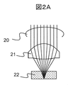
- FIG. 2A shows a state in which the glass substrate 22 is irradiated with the parallel light 20 (wavelength 780 nm) through the aspherical lens 21 for the optical disc.
- the glass substrate 22 is a glass substrate having a thickness of 1.2 mm and a refractive index of 1.5, and the aspherical lens 21 is optimized with respect to the glass substrate 22.
- 2C shows an encircled energy distribution centered on the center of the optical path on the photocathode when the parallel light 20 is focused by the aspherical lens 21.
- the spherical aberration that depends on the lens is the minimum, and only the diffraction aberration that depends on the wavelength of light is the diffraction limit that determines the focus shape.
- FIG. 2B shows a state in which parallel light 20 (wavelength 780 nm) is applied to the transparent substrate 11 through the same aspherical lens 21.
- the transparent substrate 11 is a semiconductor photocathode substrate and is a 0.4 mm thick GaP substrate.
- the GaP substrate has a refractive index of 3.2.
- the collimated light 20 is focused by the aspherical lens 21, and the energy distribution within a circle centered on the center of the optical path on the photocathode is a broken line 202 in FIG. 2C.
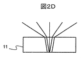
- FIG. 2D shows light rays incident on the GaP substrate 11.
- the emission of electrons from a wide area of the photoelectric film reduces the brightness of the electron source and increases the diameter of the electron source.
- the size of the electron source restricts the electron beam that can be narrowed down, and as a result, the spot diameter of the electron beam 13 on the sample becomes large, which lowers the resolution of the SEM. This is because the conditions of the refractive index and the thickness of the semiconductor photocathode do not match the design conditions of the aspherical lens 21.
- FIG. 3 shows an example of a photo-excited electron gun in which the condenser lens 2 is composed of a compound lens.
- NA Numerical Aperture
- As such an aspherical lens there is an aspherical lens formed by a glass molding method which is commercially available for optical disks.
- the condensing lens 2 is a compound lens in which the aspherical lens 21 and the correction lens 31 for minimizing the spherical aberration on the photocathode are combined to form a solid line 201 in FIG. 2C on the photocathode.
- the correction lens 31 is a convex lens, and can convert the spherical light on the focal point by correcting the light incident on the aspherical lens 21 from parallel light to convergent light.
- the root mean square (RMS) of the spherical aberration on the photoelectric film is set to ⁇ /14 or less.
- ⁇ is the wavelength of the excitation light, and corresponds to satisfying the Marechal criterion.
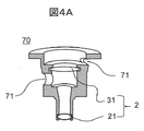
- a lens holder 70 as shown in FIG. 4A.
- the lens holder 70 coaxially fixes the aspherical lens 21 and the correction lens 31.
- the exhaust holes 71 are provided above and below the correction lens 31, respectively.
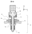
- the lens holder 70 is used by being fixed to the tip of the lens stage 72 shown in FIG. 4B.
- the movable portion 73 of the lens stage 72 is capable of integrally adjusting the position with respect to the photocathode 1 from the parallel light source 7 to the condenser lens 2 which is held by the lens holder 70 including the window 6 separating the vacuum and the atmosphere. It is said that.
- the vacuum flange 74 is fixed to the vacuum container 9.
- the movable portion 73 has the window 6 arranged at one end, the lens holder 70 arranged at the other end, and is connected to the vacuum flange 74 by a bellows 75.
- a cavity through which the excitation light passes is provided between the window 6 and the lens holder 70, and the space inside the cavity is kept in vacuum.
- the longitudinal direction of the cavity of the movable portion 73 is defined as the z axis
- the window 6 is defined as being arranged on a plane stretched by an x axis and ay axis perpendicular to the z axis.
- the movable portion 73 is adjusted in position on the xy plane by the lens stage xy adjusting screw 76 provided on the vacuum flange 74, and the z-axis (optical axis) is adjusted by the lens stage z adjusting screw 77 provided on the vacuum flange 74. Position adjustment on the axis) is performed.
- the condensing lens 2 is composed of two lenses, it is necessary to align the axis with the parallel excitation light. Therefore, the parallel light source 7 adjusts the xy position with respect to the lens stage 72. It is mounted by a four-axis optical path adjusting mechanism 78 for xy tilt adjustment. That is, the optical path adjusting mechanism 78 has two axes for adjusting the position on the zy plane and two axes for adjusting the inclination in the x-axis direction and the inclination in the y-axis direction with respect to the xy plane.
- the condenser lens 2 has the aspherical lens 21 and the correction lens 31 placed in a vacuum, but the excitation light may be incident on the aspherical lens 21 in a desired trajectory. Therefore, as shown in FIG. 5, the same effect can be obtained even when the correction lens 31 is in the atmosphere.
- the correction lens 31 having a focal length longer than that of the correction lens in the configuration of FIG. 3 is selected.
- the configuration of FIG. 5 by introducing a mechanism for adjusting the position and angle of the correction lens 31 placed in the atmosphere, it is possible to optimize the optical system more easily.
- the vacuum container 9 forming the electron gun needs to be kept in a high vacuum, it is an effective configuration that the correction lens 31 can be replaced and the orbit of excitation light by the correction lens 31 can be adjusted in the atmosphere. ..
- FIG. 6 shows the control mechanism of the lens stage 72.
- the excitation light source 43 is a laser diode or an optical fiber end.
- the divergent light from the light source 43 is converted into parallel excitation light 12 by the collimator lens 42.
- the parallel light source 7 shown in FIGS. 1 and 4B has a configuration corresponding to the light source 43 and the collimator lens 42.
- the excitation light 12 passes through the beam splitter 40, enters the vacuum container of the electron gun through the window 6, and is condensed on the photocathode 1 by the condenser lens 2.
- the reflected light 46 reflected from the photocathode becomes parallel light by the condenser lens 2, is laterally bent by the beam splitter 40, and is enlarged and projected on the image pickup element 41 by the imaging lens 44.
- the spatial distribution of the light intensity is measured by appropriately attenuating it with an ND (Neutral Density) filter 45.
- ND Neutral Density
- the focal length f of the condensing lens 2 is 4.2 mm
- the shape of the enlarged focus obtained by the image sensor 41 is monitored by a PC or the like, and the position of the lens stage 72 in the z-axis direction is adjusted so that the spot here is minimized. Optimize the excitation light focus on the cathode 1.
- the beam splitter 40 can be used as a polarization beam splitter to increase the transmittance, which is effective. Further, by inserting a quarter-wave plate directly below the beam splitter to rotate the plane of polarization of the reflected light 46 so that it does not return to the light source 43, the return light to the laser diode 43 can be minimized. Has the advantage that it can be stabilized.
- an aspherical lens for an optical disc as the aspherical lens 21
- the present invention is not limited to this, and the same effect can be obtained by properly using the correction lens 31 even if another lens is used.
- a collimator lens of a laser diode an aspherical lens that minimizes spherical aberration through a glass plate with a thickness of 0.25 mm, and an aspherical lens that minimizes spherical aberration in air or vacuum (without allowing glass to pass through). Lenses are commercially available. Even for such an aspherical lens, a high-performance electron gun using a semiconductor photocathode can be configured by adding a correction lens corresponding to the transparent substrate 11.
- the correction lens is one convex lens, but it is clear that it may be combined with other concave and convex lenses.
- the refractive index of a transparent single crystal substrate has wavelength dependence. For example, in the case of a GaP substrate, the refractive index is 3.2 when the wavelength of the excitation light is 780 nm, but it is 3.3 when the wavelength of the excitation light is 680 nm. Therefore, when the correction lens is composed of a plurality of lenses, it becomes easy to optimize the focus shape in accordance with the wavelength used.
- the present invention is also applicable to another semiconductor substrate such as a semiconductor photocathode formed on a single crystal substrate such as AlAs, GaAlAs, ZnSe, GaN, GaInN. It is possible.
- the refractive index of these substrates is 2.3 to 3.3.
- a transparent oxide may be used as the crystal growth substrate.
- a sapphire substrate can be used as a GaN-based or GaAs crystal growth substrate.
- the refractive index of the sapphire substrate is 1.75 to 1.8.
- the condenser lens 2 is configured as a compound lens, but instead of this, it may be configured as one aspherical lens.
- FIG. 7A shows an example of an aspherical lens 30 designed so that excitation light can be focused on the photocathode to the minimum diameter when passing through the transparent substrate 11 (GaP substrate) having a thickness of 0.4 mm (FIG. 7B). Show. In FIG. 7A, the aspherical lens 21 and the cross-sectional shape are shown in contrast.
- the spherical aberration of the aspherical lens 30 has a spherical aberration RMS of ⁇ /14 or less on the photoelectric film.
- ⁇ is the wavelength of the excitation light and corresponds to satisfying the Marechal condition.
- the shape of the aspherical lens 30 has a stronger converging action as it moves away from the center, as compared with the aspherical lens 21 for an optical disc. That is, by increasing the curvature as the distance from the center increases, the spherical aberration can be minimized and the excitation light can be focused to the minimum diameter on the photocathode as shown in FIG. 7B. As a result, the energy distribution within the circle by the aspherical lens 30 becomes a solid line 201 in FIG. 2C, and a diffraction-limited focus is obtained.
- the condenser lens 2 is configured as a compound lens, it is necessary to adjust the positional relationship between the aspherical lens that constitutes the compound lens and the correction lens with high accuracy.
- the condenser lens can be configured by one compound lens, the optical axis adjustment of the excitation light becomes easy. As a result, the optical path adjusting mechanism 78 can be eliminated in the lens stage shown in FIG. 4B.
- the aspherical lens 30 be optimized for the refractive index and thickness at the wavelength used.
- the photocathode 1 is an electron source using a negative electron affinity
- the electron emission surface is surface sensitive. Therefore, an activation chamber is provided adjacent to the electron gun 15, and a mechanism such as surface cleaning, Cs vapor deposition, oxygen introduction is provided so that the surface of the photoelectric film 10 that has been surface activated or deteriorated can be reactivated.
- a mechanism such as surface cleaning, Cs vapor deposition, oxygen introduction is provided so that the surface of the photoelectric film 10 that has been surface activated or deteriorated can be reactivated.
- the photocathode can be used for a long period of time. At this time, it is desirable to provide a transport mechanism for moving the photocathode 1 back and forth between the electron gun 15 and the activation chamber.
Landscapes
- Chemical & Material Sciences (AREA)
- Analytical Chemistry (AREA)
- Physics & Mathematics (AREA)
- General Physics & Mathematics (AREA)
- Optics & Photonics (AREA)
- Electron Sources, Ion Sources (AREA)
Abstract
試料上で電子ビームを2次元にスキャンさせる走査型電子線応用装置において、電子源として光励起電子源を用いる場合においても高分解能化を達成する。このため、屈折率が1.7 を超える基板(11)と光電膜(10)とを有するフォトカソード(1)と、励起光をフォトカソードに向けて集光する集光レンズ(2)と、フォトカソードに対向して配置され、励起光が集光レンズにより集光され、フォトカソードの基板を透過して入射されることにより、フォトカソードの光電膜から発生する電子ビームを加速させる引き出し電極(3)と、引き出し電極により加速された電子ビームを試料上で2次元に走査する偏向器(25)を含む電子光学系と、を有する電子線応用装置において、集光レンズの球面収差は、光電膜上で球面収差の二乗平均平方根が励起光の波長の1/14以下とする。
Description
本発明は電子顕微鏡などの電子線応用装置に関する。
高分解能の電子顕微鏡においては、従来、高輝度電子源として冷陰極電界放出電子源やショットキー電子源が使用されている。これらは、先端が小さな針形状で、仮想光源サイズは数nmから数十nmである。これに対して、負の電子親和力を利用した光励起電子源は平面状の電子源であり、光源サイズとなる励起光の焦点サイズは1μm程度と大きい。光励起電子源からの放出電子の直進性が良いために、電流密度を大きくすることで高輝度化が期待される。
特許文献1には光励起電子源が開示されている。フォトカソードとして透明基板、具体的にはガラス上にフォトカソード膜(光電膜)を貼り付けたものを用い、透明基板に近接して置いた集光レンズで励起光を光電膜上に収束することで小さな電子光源とし、ここから真空中に放出する電子線を利用する電子銃構造が示されている。高輝度化に適したフォトカソードとして、近年、特許文献2に示されるように、半導体の結晶成長技術を用いて半導体基板上にフォトカソード層を形成した半導体フォトカソードの開発が進められている。非特許文献1に示されるように、半導体フォトカソードにはショットキー電子源と同程度の特性を示すものも現れている。
Kuwahara他、「Coherence of a spin-polarized electron beam emitted from a semiconductor photocathode in a transmission electron microscope」Applied Physics Letters、Vol. 105、p.193101、2014年
非特許文献1においては、半導体フォトカソードを電子源としたTEM(Transmission Electron Microscope)が開示されている。TEMの電子光学系では、光学顕微鏡と同様に、試料の観察領域全面に電子線を照射する。TEMの分解能は試料に照射される電子線の平行度によって決定される。
これに対して、SEM(Scanning Electron Microscope)の電子光学系では電子線を小さなスポットに絞り込んで試料に照射し、電子線のスポットを試料上で2次元にスキャンすることにより像を形成する。SEMの分解能は基本的に試料に照射する電子線をどれだけ細く絞ることができるかによって決定される。例えば、非特許文献1には半導体フォトカソードを電子源としたTEMにおける試料上での電子線のスポット形状が示されているが、この例ではスポット径がおよそ1μmとなっている。これに対して、SEMの電子光学系では試料上での電子線のスポット径をnmオーダーあるいはそれ以下に絞り込む必要がある。
光励起電子源を利用する場合、集光レンズにより、フォトカソードの光電膜上に励起光の焦点を結ばせる必要がある。このとき、励起光はフォトカソードの透明基板を透過して光電膜上に焦点を結ぶことになる。特許文献1のように光電膜をガラス基板に貼り付けるフォトカソードでは、所定の厚さ、屈折率を有するガラス基板を透過させることを前提として最適に設計された集光レンズを用い、集光レンズに応じたガラス基板を用いてフォトカソードを形成することにより、低コストに電子銃を実現することができる。一方、近年の半導体フォトカソードでは結晶成長技術を用いることで、より高輝度なフォトカソードを実現している。しかしながら、特許文献1に示すような光励起電子源の光学系において従来のフォトカソードをそのまま半導体フォトカソードに置換しても、光励起電子源から射出される電子線をSEMの分解能に必要なスポット径まで絞りこむことができない。
本発明の一実施の態様である電子線応用装置は、屈折率が1.7を超える基板と光電膜とを有するフォトカソードと、励起光をフォトカソードに向けて集光する集光レンズと、フォトカソードに対向して配置され、励起光が集光レンズにより集光され、フォトカソードの基板を透過して入射されることにより、フォトカソードの光電膜から発生する電子ビームを加速させる引き出し電極と、引き出し電極により加速された電子ビームを試料上で2次元に走査する偏向器を含む電子光学系とを有し、集光レンズの球面収差は、光電膜上で球面収差の二乗平均平方根が励起光の波長の1/14以下である。
試料上で電子ビームを2次元にスキャンさせる走査型電子線応用装置において、電子源として光励起電子源を用いる場合においても高分解能化が達成される。
その他の課題と新規な特徴は、本明細書の記述および添付図面から明らかになるであろう。
以下、本発明の実施例を図面に基づいて説明する。
図1に光励起電子銃を有する電子線応用装置の概略図を示す。電子線応用装置が電子顕微鏡であるとすると、光励起電子銃15から発生した高輝度電子ビーム13は、接続された電子光学系筐体23に導かれ、電子レンズ24、偏向器25などの構成部品により顕微鏡として作用する。特に、本実施例の光励起電子銃は、電子線を絞り込んで偏向器25により試料上を2次元に走査させるSEM、STEM(Scanning Transmission Electron Microscope)の電子源として好適なものである。
電子銃15は真空容器9の外に置かれた平行光源7より発生した励起光12を窓6より真空容器9内に導入し、集光レンズ2によりフォトカソード1上に光を集束させる。フォトカソード1は、主として透明基板11と光電膜10からなり、透明基板11側から励起光を入射し、光電膜10の表面から電子ビームを発生する。電子ビーム13は、フォトカソード1と対向する引き出し電極3との間の電界により加速されて、開口部14を通過して電子光学系筐体23に入射される。フォトカソード1はカソードホルダ4に収められ、加速電源5と電気的に接続され、発生する電子ビームの加速エネルギーを規定する。フォトカソード1は負の電子親和力による電子源として知られている現象を利用するもので、光電膜10はp型の半導体であり、代表的なものとしてGaAsが用いられ、表面には仕事関数を低くするためのCs吸着などが施されている。透明基板11には光電膜10の結晶をエピタキシャル成長させるために、厚さ0.4~0.5mmのGaP(100)単結晶が使われている。
ここで、集光レンズ2は、平行光源7からの励起光12を光電膜10上の狭い範囲に集束させるために設けられている。集光レンズによる励起光の集束作用に対してフォトカソードの透明基板が与える影響について、図2A~Dを用いて説明する。図2Aは、光ディスク用の非球面レンズ21を通して平行光20(波長780nm)をガラス基板22に照射した様子を示している。ガラス基板22は厚さ1.2mm、屈折率1.5のガラス基板であり、非球面レンズ21は、ガラス基板22に対して最適化されている。このとき、平行光20が非球面レンズ21により焦点を結ぶときの光電面での光路の中心を軸とした円内エネルギー(encircled energy)分布が図2Cの実線201である。この場合、レンズに依存する球面収差は最少となり、光の波長に依存する回折収差のみが焦点形状を決定する回折限界となっている。
一方、図2Bは、同じ非球面レンズ21を通して平行光20(波長780nm)を透明基板11に照射した様子を示している。透明基板11は、半導体フォトカソードの基板であり、厚さ0.4mmのGaP基板とする。GaP基板の屈折率は3.2である。平行光20が非球面レンズ21により集束され、光電面での光路の中心を軸とした円内エネルギー分布が図2Cの破線202である。実線201の円内エネルギー分布が光路中心の狭い範囲に集中しているのに比べ、破線202の円内エネルギー分布は光路中心から広く分散していることが分かる。図2DにGaP基板11に入射する光線を示す。このように、レンズ21の中心部を通る光路が収束する光軸方向の位置とレンズ21の周辺部を通る光路が収束する光軸方向の位置がずれているために、光電面において平行光20を十分に集束させることができない。すなわち、大きな球面収差が生じている。光電膜の広い領域から電子が放出されることにより、電子源の輝度が低下するとともに、電子源の径が大きくなる。電子源の大きさが、絞り込み可能な電子ビームを制約し、その結果試料上における電子ビーム13のスポット径が大きくなり、SEMの解像度を低下させる。これは、半導体フォトカソードの屈折率と厚みの条件が、非球面レンズ21の設計条件とあっていないことが原因である。
実施例1として、図3に集光レンズ2を複合レンズで構成した光励起電子銃の例を示す。非球面レンズ21は、焦点距離f=4.2mm、NA(Numerical Aperture)は0.5であり、厚さ1.2mm、屈折率1.5のガラス板を通したときに最小径に集光できるように設計されている。このような非球面レンズとして、光ディスク用に市販されているガラスモールド法で形成した非球面レンズがある。実施例1では、集光レンズ2を、非球面レンズ21に光電面での球面収差を最小にするための補正レンズ31を組み合わせた複合レンズとすることで、光電面上に図2Cの実線201として示されるような最適焦点を得るものである。補正レンズ31は凸レンズであり、非球面レンズ21に入射する光を、平行光から収束光に変換することで、焦点上の球面収差を補正可能とできる。複合レンズによる球面収差は光電膜上で球面収差の二乗平均平方根(RMS:root mean square)がλ/14以下とする。ここで、λは励起光の波長であり、マレシャル条件(Marechal criterion)を満たすことに相当する。
例えば、透明基板11(GaP基板)の厚さが0.4mm、励起光波長780nmの場合、焦点距離f=60mmの補正レンズ31を、非球面レンズ21との距離を20mmから35mmの距離に固定して用いる。複合レンズの相互の位置関係の精度は、球面収差の補正の程度に大きく影響するため、図4Aに示すようなレンズホルダ70により、複合レンズを保持することが好ましい。レンズホルダ70は、非球面レンズ21と補正レンズ31とを同軸上に固定する。この場合、補正レンズ31の上下は電子銃の真空容器9内に置かれるので、排気孔71を補正レンズ31の上下それぞれに設ける。レンズホルダ70は、図4Bに示すレンズステージ72の先端に固定して用いる。レンズステージ72の可動部73は、平行光源7から、真空と大気とを隔てる窓6を含んでレンズホルダ70に保持される集光レンズ2までを一体として、フォトカソード1に対して位置調整可能とされている。図4Bの構成では、真空フランジ74が真空容器9に固定されている。可動部73は一方の端部に窓6が配置され、他方の端部にレンズホルダ70が配置され、ベローズ75で真空フランジ74に接続されている。また、窓6からレンズホルダ70との間に励起光が通過する空洞が設けられ、空洞内の空間は真空に保たれている。ここで、可動部73の空洞の長手方向をz軸とし、窓6は前記z軸と垂直なx軸とy軸とで張られる平面に配置されていると定義する。可動部73は、真空フランジ74に設けられたレンズステージx-y調節ネジ76によりx-y平面上の位置調整が、また真空フランジ74に設けられたレンズステージz調節ネジ77によりz軸(光軸)上の位置調整がなされる。
また、集光レンズ2は2枚のレンズで構成されているために、平行な励起光との軸あわせが必要となるため、平行光源7はレンズステージ72に対して、x-y位置調節とx-y傾き調節の4軸の光路調整機構78によりマウントされている。すなわち、光路調整機構78は、zy平面上の位置を調整する2軸と、xy平面に対するx軸方向の傾き及びy軸方向の傾きを調整する2軸とを有している。
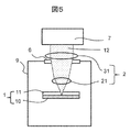
図3の例では、集光レンズ2として、非球面レンズ21と補正レンズ31とを真空中に置いた構成としたが、非球面レンズ21に対して励起光が所望の軌道で入射すればよいので、図5のように、補正レンズ31を大気中においても同様の効果が得られる。この場合の補正レンズ31は図3の構成における補正レンズよりも焦点距離の長いものが選ばれる。図5の構成の場合、大気中に置いた補正レンズ31の位置と角度を調節する機構を導入することにより、光学系の最適化がよりしやすくなるという効果がある。特に、電子銃を構成する真空容器9は高真空に保たれる必要があるため、補正レンズ31の交換や、補正レンズ31による励起光の軌道調整を大気中で行えるのは有効な構成である。
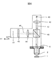
図6にレンズステージ72の制御機構を示す。励起光の光源43は、レーザーダイオードもしくは光ファイバー端である。光源43からの発散光はコリメータレンズ42で平行な励起光12にされる。図1や図4B等の平行光源7は、光源43及びコリメータレンズ42に相当する構成である。励起光12はビームスプリッタ40を通過して窓6から電子銃の真空容器内に入り、集光レンズ2によりフォトカソード1に集光される。光電面から反射された反射光46は集光レンズ2により平行光となり、ビームスプリッタ40により横に曲げられ、結像レンズ44により撮像素子41上に拡大投影される。反射光46の強度が撮像素子41にとって高すぎる場合は、ND(Neutral Density)フィルタ45により適宜減衰させて光強度の空間分布を測定する。ここで、集光レンズ2の焦点距離fが4.2mmである場合、結像レンズ44に焦点距離f=100mmのレンズを用いると、撮像素子41上に光電膜上の23.8倍の像が投影されるため、この出力をPCなどでモニターすることで、フォトカソード1の光電面に集束された励起光焦点の像を観察できる。焦点調整にあたっては撮像素子41で得られた拡大焦点の形状をPCなどによりモニターしながら、ここでのスポットが最小となるように、レンズステージ72のz軸方向の位置調整を行うことにより、フォトカソード1上の励起光焦点を最適化する。
なお、光源43からの励起光12が偏光している場合、ビームスプリッタ40を偏光ビームスプリッタとして透過率を大きくすることができ、効果的である。さらにビームスプリッタ直下に1/4波長板を入れることにより、反射光46の偏光面を回転させて光源43に戻らないようにすることで、レーザーダイオード43への戻り光を最小にできるので、動作を安定化できるという利点がある。
なお、非球面レンズ21として光ディスク用の非球面レンズを用いる例を説明したが、これに限られず、他のレンズを用いても補正レンズ31を適正に用いることで同様の効果が得られる。たとえば、レーザーダイオードのコリメータレンズ向けに、厚さ0.25mmのガラス板を通して球面収差を最小にする非球面レンズ、大気中あるいは真空中で(ガラス等を透過させないで)球面収差を最小にする非球面レンズが市販されている。このような非球面レンズに対しても、透明基板11に応じた補正レンズを追加することで、半導体フォトカソードをもちいた高性能の電子銃を構成可能である。
また、補正レンズは1枚の凸レンズとしたが、他の凹レンズ、凸レンズと組み合わせてもよいことは明らかである。一般に透明単結晶基板の屈折率には波長依存性がある。例えば、GaP基板の場合、励起光の波長が780nmの場合の屈折率は3.2であるが、励起光の波長が680nmの場合の屈折率は3.3である。このため、補正レンズが複数のレンズで構成されている場合には、使用する波長にあわせて焦点形状を最適化することも容易になる。
さらに、透明基板11としてGaP基板を用いる例を示したが、他の半導体基板として、例えばAlAs、GaAlAs、ZnSe、GaN、GaInNなどの単結晶基板上に形成された半導体フォトカソードに対しても適用可能である。これらの基板の屈折率は2.3から3.3である。また、結晶成長基板として透明な酸化物を用いてもよい。例えば、GaN系やGaAs等の結晶成長基板として、サファイヤ基板を使用することが可能である。サファイヤ基板の屈折率は1.75~1.8である。
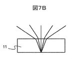
実施例1では、集光レンズ2を複合レンズとして構成したが、これに代えて1つの非球面レンズとして構成することも可能である。図7Aに、厚さが0.4mmの透明基板11(GaP基板)を通した場合に、励起光を光電面に最小径に集束できる(図7B)ように設計された非球面レンズ30の例を示す。図7Aでは、非球面レンズ21と断面形状を対比させて示している。具体的には、非球面レンズ30により集束された励起光の焦点形状を回折限界で決まるサイズにするために、非球面レンズ30の球面収差は光電膜上で球面収差のRMSがλ/14以下とする。ここで、λは励起光の波長であり、マレシャル条件を満たすことに相当する。
非球面レンズ30の形状は、光ディスク用の非球面レンズ21に比べて、中心から離れるにつれて収束作用を強くしている。すなわち、中心から離れるにつれて曲率をより大きくすることで、球面収差を最小化し、図7Bに示すように光電面にて最小径に励起光を集束させることができる。この結果、非球面レンズ30による円内エネルギー分布は図2Cの実線201となり、回折限界の焦点が得られる。
実施例1の場合、集光レンズ2を複合レンズとして構成しているため、複合レンズを構成する非球面レンズと補正レンズとの位置関係の調整を高精度に行う必要がある。これに対して、実施例2の場合は、集光レンズが1枚の複合レンズで構成できるため、励起光の光軸調整が容易になる。この結果、図4Bに示したレンズステージにおいて、光路調整機構78を不要とすることができる。
なお、上述のように透明単結晶基板の屈折率は波長依存性があるために、非球面レンズ30は、使用する波長での屈折率と厚さに最適化されていることが望ましい。
以上、本発明者によってなされた発明を実施の形態に基づき具体的に説明したが、本発明は実施の形態に限定されるものではなく、その要旨を逸脱しない範囲で種々変更可能である。例えば、フォトカソード1が負の電子親和力を利用した電子源の場合、電子放出面が表面敏感である。このため、電子銃15に隣接して活性化室を設け、表面清浄化や、Cs蒸着、酸素導入などの機構を備えて、表面活性化や劣化した光電膜10表面を再活性化できるようにすると、フォトカソードを長期間使用できるという利点がある。このとき、フォトカソード1を電子銃15と活性化室との間で行き来させる搬送機構を設けることが望ましい。
1:フォトカソード、2:集光レンズ、3:引き出し電極、4:カソードホルダ、5:加速電源、6:窓、7:平行光源、9:真空容器、10:光電膜、11:透明基板、12:励起光、13:電子ビーム、14:開口部、15:光励起電子銃、20:平行光、21:光ディスク用非球面レンズ、22:ガラス基板、23:電子光学系筐体、24:電子レンズ、25:偏向器、30:GaP基板用非球面レンズ、31:補正レンズ、40:ビームスプリッタ、41:撮像素子、42:コリメータレンズ、43:光源、44:結像レンズ、45:NDフィルタ、46:反射光、70:レンズホルダ、71:排気孔、72:レンズステージ、73:可動部、74:真空フランジ、75:ベローズ、76:レンズステージx-y調節ネジ、77:レンズステージz調節ネジ、78:光路調整機構。
Claims (8)
- 屈折率が1.7を超える基板と光電膜とを有するフォトカソードと、
励起光を前記フォトカソードに向けて集光する集光レンズと、
前記フォトカソードに対向して配置され、前記励起光が前記集光レンズにより集光され、前記フォトカソードの基板を透過して入射されることにより、前記フォトカソードの光電膜から発生する電子ビームを加速させる引き出し電極と、
前記引き出し電極により加速された前記電子ビームを試料上で2次元に走査する偏向器を含む電子光学系とを有し、
前記集光レンズの球面収差は、前記光電膜上で前記球面収差の二乗平均平方根が前記励起光の波長の1/14以下である電子線応用装置。 - 請求項1において、
前記フォトカソードの前記光電膜は、前記励起光に対して透明な単結晶基板上に結晶をエピタキシャル成長させて形成された電子線応用装置。 - 請求項1において、
前記集光レンズは、非球面レンズからなる電子線応用装置。 - 請求項1において、
前記集光レンズは、非球面レンズと少なくとも1枚の凸レンズとを含む複合レンズである電子線応用装置。 - 請求項4において、
前記引き出し電極及び前記フォトカソードが配置される真空容器と、
前記複合レンズを保持するレンズステージと、
前記レンズステージは、
前記真空容器に固定される真空フランジと、
前記真空フランジに対して可動に取り付けられ、一方の端部に前記励起光を入射させるための窓を有し、他方の端部に前記複合レンズを保持するレンズホルダを有し、前記窓と前記レンズホルダとの間に前記励起光を通過させるための空洞が設けられた可動部とを有する電子線応用装置。 - 請求項5において、
前記複合レンズの前記凸レンズは、前記レンズホルダにおいて前記非球面レンズよりも前記窓側で保持されており、前記レンズホルダは前記凸レンズの上下において前記真空容器と前記レンズホルダ内の空間とを導通させる排気孔を有する電子線応用装置。 - 請求項5において、
前記励起光を平行光として出射する光源とを有し、
前記光源は光路調整機構を介して前記レンズステージにマウントされ、
前記可動部の前記空洞の長手方向をz軸とし、前記窓が前記z軸と垂直なx軸とy軸とで張られる平面にあるとき、前記光路調整機構は、xy平面上の位置を調整する2軸と、xy平面に対するx軸方向の傾き及びy軸方向の傾きを調整する2軸とを有する電子線応用装置。 - 請求項4において、
前記引き出し電極及び前記フォトカソードが配置される真空容器を有し、
前記非球面レンズは前記真空容器内の真空中に配置され、前記凸レンズは大気中に配置される電子線応用装置。
Priority Applications (3)
| Application Number | Priority Date | Filing Date | Title |
|---|---|---|---|
| PCT/JP2019/002803 WO2020157809A1 (ja) | 2019-01-28 | 2019-01-28 | 電子線応用装置 |
| JP2020568899A JP7106685B2 (ja) | 2019-01-28 | 2019-01-28 | 電子線応用装置 |
| US17/425,872 US11784022B2 (en) | 2019-01-28 | 2019-01-28 | Electron beam apparatus |
Applications Claiming Priority (1)
| Application Number | Priority Date | Filing Date | Title |
|---|---|---|---|
| PCT/JP2019/002803 WO2020157809A1 (ja) | 2019-01-28 | 2019-01-28 | 電子線応用装置 |
Publications (1)
| Publication Number | Publication Date |
|---|---|
| WO2020157809A1 true WO2020157809A1 (ja) | 2020-08-06 |
Family
ID=71842111
Family Applications (1)
| Application Number | Title | Priority Date | Filing Date |
|---|---|---|---|
| PCT/JP2019/002803 Ceased WO2020157809A1 (ja) | 2019-01-28 | 2019-01-28 | 電子線応用装置 |
Country Status (3)
| Country | Link |
|---|---|
| US (1) | US11784022B2 (ja) |
| JP (1) | JP7106685B2 (ja) |
| WO (1) | WO2020157809A1 (ja) |
Cited By (1)
| Publication number | Priority date | Publication date | Assignee | Title |
|---|---|---|---|---|
| US20230048762A1 (en) * | 2021-07-28 | 2023-02-16 | The University Of Massachusetts | Facade system for thermally conditioning buildings |
Families Citing this family (1)
| Publication number | Priority date | Publication date | Assignee | Title |
|---|---|---|---|---|
| JP3470047B2 (ja) | 1998-09-08 | 2003-11-25 | 西川化成株式会社 | 自動車用空気調和装置 |
Citations (6)
| Publication number | Priority date | Publication date | Assignee | Title |
|---|---|---|---|---|
| JPH1020198A (ja) * | 1996-07-02 | 1998-01-23 | Olympus Optical Co Ltd | 近赤外線顕微鏡及びこれを用いた顕微鏡観察システム |
| JP2003303565A (ja) * | 2002-04-10 | 2003-10-24 | Hitachi High-Technologies Corp | 電子線検査装置 |
| JP2017054954A (ja) * | 2015-09-10 | 2017-03-16 | 株式会社東芝 | 発光装置 |
| WO2017168554A1 (ja) * | 2016-03-29 | 2017-10-05 | 株式会社日立ハイテクノロジーズ | 電子顕微鏡 |
| US20180337017A1 (en) * | 2017-05-16 | 2018-11-22 | International Business Machines Corporation | Measuring spherical and chromatic aberrations in cathode lens electrode microscopes |
| US20190013176A1 (en) * | 2017-07-05 | 2019-01-10 | ICT Integrated Circuit Testing Gesellschaft für Halbleiterprüftechnik mbH | Aberration-corrected multibeam source, charged particle beam device and method of imaging or illuminating a specimen with an array of primary charged particle beamlets |
Family Cites Families (18)
| Publication number | Priority date | Publication date | Assignee | Title |
|---|---|---|---|---|
| JP2530591B2 (ja) | 1984-10-12 | 1996-09-04 | 慶治 矢田 | 大電流密度の電子放出に適するパルス状レ−ザ−光励起による電子源装置 |
| US5932966A (en) | 1995-07-10 | 1999-08-03 | Intevac, Inc. | Electron sources utilizing patterned negative electron affinity photocathodes |
| US5684360A (en) | 1995-07-10 | 1997-11-04 | Intevac, Inc. | Electron sources utilizing negative electron affinity photocathodes with ultra-small emission areas |
| US5898269A (en) * | 1995-07-10 | 1999-04-27 | The Board Of Trustees Of The Leland Stanford Jr. University | Electron sources having shielded cathodes |
| US6005247A (en) | 1997-10-01 | 1999-12-21 | Intevac, Inc. | Electron beam microscope using electron beam patterns |
| JP2001143648A (ja) | 1999-11-17 | 2001-05-25 | Hitachi Ltd | 光励起電子線源および電子線応用装置 |
| JP2001176120A (ja) | 1999-12-17 | 2001-06-29 | Olympus Optical Co Ltd | 光ピックアップ装置 |
| US6828574B1 (en) | 2000-08-08 | 2004-12-07 | Applied Materials, Inc. | Modulator driven photocathode electron beam generator |
| JP3987276B2 (ja) | 2000-10-12 | 2007-10-03 | 株式会社日立製作所 | 試料像形成方法 |
| US20030048427A1 (en) * | 2001-01-31 | 2003-03-13 | Applied Materials, Inc. | Electron beam lithography system having improved electron gun |
| US7250618B2 (en) | 2005-02-02 | 2007-07-31 | Nikon Corporation | Radiantly heated cathode for an electron gun and heating assembly |
| US7573053B2 (en) | 2006-03-30 | 2009-08-11 | Uchicago Argonne, Llc | Polarized pulsed front-end beam source for electron microscope |
| JP2008294124A (ja) | 2007-05-23 | 2008-12-04 | Fujitsu Ltd | 光半導体素子 |
| WO2009119074A1 (ja) | 2008-03-25 | 2009-10-01 | 国立大学法人名古屋大学 | スピン偏極電子発生素子 |
| JP5354657B2 (ja) | 2009-03-17 | 2013-11-27 | 独立行政法人理化学研究所 | 偏極電子銃、偏極電子線の発生方法、電子銃の評価方法、及び逆光電子分光方法 |
| WO2011122171A1 (ja) | 2010-03-29 | 2011-10-06 | 国立大学法人名古屋大学 | 電子顕微鏡 |
| EP2622330B1 (en) | 2010-10-01 | 2014-12-17 | Attolight SA | Deconvolution of time-gated cathodoluminescence images |
| JP6496894B1 (ja) * | 2017-11-09 | 2019-04-10 | 株式会社 彩世 | 光学素子及びレーザ照射装置 |
-
2019
- 2019-01-28 WO PCT/JP2019/002803 patent/WO2020157809A1/ja not_active Ceased
- 2019-01-28 JP JP2020568899A patent/JP7106685B2/ja active Active
- 2019-01-28 US US17/425,872 patent/US11784022B2/en active Active
Patent Citations (6)
| Publication number | Priority date | Publication date | Assignee | Title |
|---|---|---|---|---|
| JPH1020198A (ja) * | 1996-07-02 | 1998-01-23 | Olympus Optical Co Ltd | 近赤外線顕微鏡及びこれを用いた顕微鏡観察システム |
| JP2003303565A (ja) * | 2002-04-10 | 2003-10-24 | Hitachi High-Technologies Corp | 電子線検査装置 |
| JP2017054954A (ja) * | 2015-09-10 | 2017-03-16 | 株式会社東芝 | 発光装置 |
| WO2017168554A1 (ja) * | 2016-03-29 | 2017-10-05 | 株式会社日立ハイテクノロジーズ | 電子顕微鏡 |
| US20180337017A1 (en) * | 2017-05-16 | 2018-11-22 | International Business Machines Corporation | Measuring spherical and chromatic aberrations in cathode lens electrode microscopes |
| US20190013176A1 (en) * | 2017-07-05 | 2019-01-10 | ICT Integrated Circuit Testing Gesellschaft für Halbleiterprüftechnik mbH | Aberration-corrected multibeam source, charged particle beam device and method of imaging or illuminating a specimen with an array of primary charged particle beamlets |
Non-Patent Citations (1)
| Title |
|---|
| IZUMITANI,TETSURO.: "High Precision Moulding of Aspherical Glass Lenses", JOURNAL OF THE JAPAN SOCIETY OF PRECISION ENGINEERING, vol. 55, no. 6, 5 June 1989 (1989-06-05), JP, pages 972 - 975, XP009522780, ISSN: 0912-0289, DOI: 10.2493/jjspe.55.972 * |
Cited By (2)
| Publication number | Priority date | Publication date | Assignee | Title |
|---|---|---|---|---|
| US20230048762A1 (en) * | 2021-07-28 | 2023-02-16 | The University Of Massachusetts | Facade system for thermally conditioning buildings |
| US12435889B2 (en) * | 2021-07-28 | 2025-10-07 | The University Of Massachusetts | Facade system for thermally conditioning buildings |
Also Published As
| Publication number | Publication date |
|---|---|
| JP7106685B2 (ja) | 2022-07-26 |
| JPWO2020157809A1 (ja) | 2021-11-25 |
| US11784022B2 (en) | 2023-10-10 |
| US20220165536A1 (en) | 2022-05-26 |
Similar Documents
| Publication | Publication Date | Title |
|---|---|---|
| US11251011B2 (en) | Electron microscope | |
| NZ245008A (en) | Image intensifier tube transmission mode photocathode with indium-gallium-arsenide active layer | |
| JP2001143648A (ja) | 光励起電子線源および電子線応用装置 | |
| JP7106685B2 (ja) | 電子線応用装置 | |
| WO2021192070A1 (ja) | 電子銃及び電子顕微鏡 | |
| JP2002313273A (ja) | 電子顕微鏡装置 | |
| US6759800B1 (en) | Diamond supported photocathodes for electron sources | |
| JP6945071B2 (ja) | 電子線応用装置 | |
| JP2000123716A (ja) | 微小電子源 | |
| US20190341217A1 (en) | Optically addressed, thermionic electron beam device | |
| CN111293586A (zh) | 一种用于激光照明的半导体激光偏振合束装置 | |
| US12165828B2 (en) | Electron gun and electron beam application apparatus | |
| TWI898362B (zh) | 電子發射器,使用該電子發射器的電子源及多電子束裝置 | |
| US20260039093A1 (en) | Laser module and laser processing machine | |
| WO2023248272A1 (ja) | 電子顕微鏡およびその画像撮影方法 | |
| US20240161997A1 (en) | Electron beam application device | |
| WO2023233657A1 (ja) | 電子線応用装置及び電子ビーム発生方法 | |
| KR20250016307A (ko) | 고휘도 x-선 소스 | |
| CN120836076A (zh) | 用于生成x射线束的光学设备 | |
| WO2025220072A1 (ja) | 電子顕微鏡 | |
| Mano et al. | Laser Focusing System for High Brightness Polarized Electron Source for SPLEEM | |
| JPH07161321A (ja) | 電子顕微鏡の電子銃 |
Legal Events
| Date | Code | Title | Description |
|---|---|---|---|
| 121 | Ep: the epo has been informed by wipo that ep was designated in this application |
Ref document number: 19912347 Country of ref document: EP Kind code of ref document: A1 |
|
| ENP | Entry into the national phase |
Ref document number: 2020568899 Country of ref document: JP Kind code of ref document: A |
|
| NENP | Non-entry into the national phase |
Ref country code: DE |
|
| 122 | Ep: pct application non-entry in european phase |
Ref document number: 19912347 Country of ref document: EP Kind code of ref document: A1 |