WO2020152523A1 - 半導体装置、半導体装置の作製方法、及び半導体装置の動作方法 - Google Patents
半導体装置、半導体装置の作製方法、及び半導体装置の動作方法 Download PDFInfo
- Publication number
- WO2020152523A1 WO2020152523A1 PCT/IB2019/059962 IB2019059962W WO2020152523A1 WO 2020152523 A1 WO2020152523 A1 WO 2020152523A1 IB 2019059962 W IB2019059962 W IB 2019059962W WO 2020152523 A1 WO2020152523 A1 WO 2020152523A1
- Authority
- WO
- WIPO (PCT)
- Prior art keywords
- insulator
- oxide
- conductor
- transistor
- semiconductor device
- Prior art date
- Legal status (The legal status is an assumption and is not a legal conclusion. Google has not performed a legal analysis and makes no representation as to the accuracy of the status listed.)
- Ceased
Links
Images


Classifications
-
- H—ELECTRICITY
- H10—SEMICONDUCTOR DEVICES; ELECTRIC SOLID-STATE DEVICES NOT OTHERWISE PROVIDED FOR
- H10B—ELECTRONIC MEMORY DEVICES
- H10B43/00—EEPROM devices comprising charge-trapping gate insulators
- H10B43/20—EEPROM devices comprising charge-trapping gate insulators characterised by three-dimensional [3D] arrangements, e.g. with cells on different height levels
- H10B43/23—EEPROM devices comprising charge-trapping gate insulators characterised by three-dimensional [3D] arrangements, e.g. with cells on different height levels with source and drain on different levels, e.g. with sloping channels
- H10B43/27—EEPROM devices comprising charge-trapping gate insulators characterised by three-dimensional [3D] arrangements, e.g. with cells on different height levels with source and drain on different levels, e.g. with sloping channels the channels comprising vertical portions, e.g. U-shaped channels
-
- G—PHYSICS
- G11—INFORMATION STORAGE
- G11C—STATIC STORES
- G11C16/00—Erasable programmable read-only memories
- G11C16/02—Erasable programmable read-only memories electrically programmable
- G11C16/04—Erasable programmable read-only memories electrically programmable using variable threshold transistors, e.g. FAMOS
- G11C16/0483—Erasable programmable read-only memories electrically programmable using variable threshold transistors, e.g. FAMOS comprising cells having several storage transistors connected in series
-
- G—PHYSICS
- G11—INFORMATION STORAGE
- G11C—STATIC STORES
- G11C16/00—Erasable programmable read-only memories
- G11C16/02—Erasable programmable read-only memories electrically programmable
- G11C16/04—Erasable programmable read-only memories electrically programmable using variable threshold transistors, e.g. FAMOS
- G11C16/0466—Erasable programmable read-only memories electrically programmable using variable threshold transistors, e.g. FAMOS comprising cells with charge storage in an insulating layer, e.g. metal-nitride-oxide-silicon [MNOS], silicon-oxide-nitride-oxide-silicon [SONOS]
-
- G—PHYSICS
- G11—INFORMATION STORAGE
- G11C—STATIC STORES
- G11C16/00—Erasable programmable read-only memories
- G11C16/02—Erasable programmable read-only memories electrically programmable
- G11C16/06—Auxiliary circuits, e.g. for writing into memory
- G11C16/10—Programming or data input circuits
- G11C16/14—Circuits for erasing electrically, e.g. erase voltage switching circuits
-
- G—PHYSICS
- G11—INFORMATION STORAGE
- G11C—STATIC STORES
- G11C16/00—Erasable programmable read-only memories
- G11C16/02—Erasable programmable read-only memories electrically programmable
- G11C16/06—Auxiliary circuits, e.g. for writing into memory
- G11C16/26—Sensing or reading circuits; Data output circuits
-
- G—PHYSICS
- G11—INFORMATION STORAGE
- G11C—STATIC STORES
- G11C16/00—Erasable programmable read-only memories
- G11C16/02—Erasable programmable read-only memories electrically programmable
- G11C16/06—Auxiliary circuits, e.g. for writing into memory
- G11C16/32—Timing circuits
-
- H—ELECTRICITY
- H10—SEMICONDUCTOR DEVICES; ELECTRIC SOLID-STATE DEVICES NOT OTHERWISE PROVIDED FOR
- H10B—ELECTRONIC MEMORY DEVICES
- H10B41/00—Electrically erasable-and-programmable ROM [EEPROM] devices comprising floating gates
- H10B41/20—Electrically erasable-and-programmable ROM [EEPROM] devices comprising floating gates characterised by three-dimensional [3D] arrangements, e.g. with cells on different height levels
- H10B41/23—Electrically erasable-and-programmable ROM [EEPROM] devices comprising floating gates characterised by three-dimensional [3D] arrangements, e.g. with cells on different height levels with source and drain on different levels, e.g. with sloping channels
- H10B41/27—Electrically erasable-and-programmable ROM [EEPROM] devices comprising floating gates characterised by three-dimensional [3D] arrangements, e.g. with cells on different height levels with source and drain on different levels, e.g. with sloping channels the channels comprising vertical portions, e.g. U-shaped channels
-
- H—ELECTRICITY
- H10—SEMICONDUCTOR DEVICES; ELECTRIC SOLID-STATE DEVICES NOT OTHERWISE PROVIDED FOR
- H10B—ELECTRONIC MEMORY DEVICES
- H10B43/00—EEPROM devices comprising charge-trapping gate insulators
- H10B43/40—EEPROM devices comprising charge-trapping gate insulators characterised by the peripheral circuit region
-
- H—ELECTRICITY
- H10—SEMICONDUCTOR DEVICES; ELECTRIC SOLID-STATE DEVICES NOT OTHERWISE PROVIDED FOR
- H10D—INORGANIC ELECTRIC SEMICONDUCTOR DEVICES
- H10D30/00—Field-effect transistors [FET]
- H10D30/60—Insulated-gate field-effect transistors [IGFET]
- H10D30/67—Thin-film transistors [TFT]
-
- H—ELECTRICITY
- H10—SEMICONDUCTOR DEVICES; ELECTRIC SOLID-STATE DEVICES NOT OTHERWISE PROVIDED FOR
- H10D—INORGANIC ELECTRIC SEMICONDUCTOR DEVICES
- H10D62/00—Semiconductor bodies, or regions thereof, of devices having potential barriers
- H10D62/80—Semiconductor bodies, or regions thereof, of devices having potential barriers characterised by the materials
-
- H—ELECTRICITY
- H10—SEMICONDUCTOR DEVICES; ELECTRIC SOLID-STATE DEVICES NOT OTHERWISE PROVIDED FOR
- H10D—INORGANIC ELECTRIC SEMICONDUCTOR DEVICES
- H10D84/00—Integrated devices formed in or on semiconductor substrates that comprise only semiconducting layers, e.g. on Si wafers or on GaAs-on-Si wafers
- H10D84/01—Manufacture or treatment
- H10D84/0123—Integrating together multiple components covered by H10D12/00 or H10D30/00, e.g. integrating multiple IGBTs
- H10D84/0126—Integrating together multiple components covered by H10D12/00 or H10D30/00, e.g. integrating multiple IGBTs the components including insulated gates, e.g. IGFETs
-
- H—ELECTRICITY
- H10—SEMICONDUCTOR DEVICES; ELECTRIC SOLID-STATE DEVICES NOT OTHERWISE PROVIDED FOR
- H10D—INORGANIC ELECTRIC SEMICONDUCTOR DEVICES
- H10D84/00—Integrated devices formed in or on semiconductor substrates that comprise only semiconducting layers, e.g. on Si wafers or on GaAs-on-Si wafers
- H10D84/01—Manufacture or treatment
- H10D84/02—Manufacture or treatment characterised by using material-based technologies
- H10D84/03—Manufacture or treatment characterised by using material-based technologies using Group IV technology, e.g. silicon technology or silicon-carbide [SiC] technology
- H10D84/038—Manufacture or treatment characterised by using material-based technologies using Group IV technology, e.g. silicon technology or silicon-carbide [SiC] technology using silicon technology, e.g. SiGe
-
- H—ELECTRICITY
- H10—SEMICONDUCTOR DEVICES; ELECTRIC SOLID-STATE DEVICES NOT OTHERWISE PROVIDED FOR
- H10P—GENERIC PROCESSES OR APPARATUS FOR THE MANUFACTURE OR TREATMENT OF DEVICES COVERED BY CLASS H10
- H10P14/00—Formation of materials, e.g. in the shape of layers or pillars
- H10P14/20—Formation of materials, e.g. in the shape of layers or pillars of semiconductor materials
- H10P14/34—Deposited materials, e.g. layers
- H10P14/3402—Deposited materials, e.g. layers characterised by the chemical composition
- H10P14/3434—Deposited materials, e.g. layers characterised by the chemical composition being oxide semiconductor materials
Definitions
- the present invention relates to a semiconductor device, for example.
- the present invention relates to a method for manufacturing a semiconductor device, for example.
- the present invention relates to a memory transistor included in a semiconductor device and a method for manufacturing the memory transistor, for example.
- the present invention relates to, for example, a method for operating a semiconductor device.
- the present invention relates to, for example, a storage device, a processor, and an electronic device.
- the present invention relates to a method for manufacturing a memory device, a processor, or an electronic device.
- the present invention relates to a method for operating a storage device, a processor, or an electronic device.
- one embodiment of the present invention is not limited to the above technical field.
- the technical field of one embodiment of the invention disclosed in this specification and the like relates to an object, a method, or a manufacturing method.
- one embodiment of the present invention relates to a process, a machine, a manufacture, or a composition (composition of matter).
- a semiconductor device refers to all devices that can function by utilizing semiconductor characteristics.
- a display device, a light-emitting device, a lighting device, an electro-optical device, a storage device, a semiconductor circuit, and an electronic device may include a semiconductor device.
- Patent Document 1 and Patent Document 2 a plurality of memory elements (also referred to as memory cells) are stacked, and a memory cell array (also referred to as a memory string) having a three-dimensional structure is formed by connecting these in series. ing.
- a memory cell array having a three-dimensional structure the larger the number of stacked memory elements, the higher the series resistance between the memory cells and the higher the resistance of the memory cell array. Due to the increased resistance of the memory cell array, there are problems such as loss of current flowing through the memory cell array and heat generation of the memory cell array.
- the semiconductor pattern provided in a column shape is in contact with the insulator having the charge storage layer.
- a semiconductor pattern provided in a columnar shape is in contact with an insulator functioning as a tunnel dielectric.
- a trap center may be formed at the interface between them.
- the trap center formed at the interface between the semiconductor and the insulator traps electrons and changes the threshold voltage of the transistor in the positive direction, so that the current driving force in the on state of the transistor, that is, the on-current and the electric field are increased. Effectiveness Mobility and reliability may be adversely affected.
- Another object of one embodiment of the present invention is to provide a module including the semiconductor device. Another object of one embodiment of the present invention is to provide an electronic device including the semiconductor device or the module. Another object of one embodiment of the present invention is to provide a novel semiconductor device. Another object of one embodiment of the present invention is to provide a novel module. Another object of one embodiment of the present invention is to provide a novel electronic device.
- One embodiment of the present invention includes a stack, the stack including a first insulator, a first conductor over the first insulator, and a second conductor over the first conductor.
- An insulator an oxide located inside a first opening provided in the first insulator, the first conductor, and the second insulator; and an oxide located outside the oxide in the first opening.
- a fourth insulating material located on the side surface of the first opening, a tunnel insulating layer located outside the oxide, and a gate insulating layer. And a charge storage layer located between the tunnel insulating layers.
- the stack has a third conductor which is positioned above the first insulator and a fifth conductor which is provided on the third conductor.
- a body, and the second opening is located in a region overlapping with the first opening.
- the oxide in the structure of (1) or (2), includes a first layer, a second layer provided in contact with the inside of the first layer, and a second layer.
- a third layer provided in contact with the inner side of the second layer, the energy gap of the second layer is narrower than the energy gap of the first layer, and the energy gap of the second layer is The semiconductor device is narrower than the energy gap of the third layer.
- one embodiment of the present invention is a semiconductor device in which in the above structure (3), the oxide contains at least indium.
- one embodiment of the present invention is a semiconductor device in which in the structure of (3) above, the oxide includes In, an element M (M is Al, Ga, Y, or Sn), and Zn. ..
- Another embodiment of the present invention is the semiconductor device according to any one of the above structures (1) to (7), including a control circuit, the control circuit being located below the stack.
- a first insulator is formed, a first conductor is formed over the first insulator, and a second insulator is formed over the first conductor. Then, the second insulator, the first conductor, and the first insulator are processed to form a first stacked body having a first opening, and the first insulator is formed in the first opening.
- a third insulator is formed so as to be in contact with the first conductor and the second insulator, an oxide is formed so as to be in contact with the third insulator, and a fourth insulator is formed so as to be in contact with the oxide.
- an insulator is formed and a second conductor is formed so as to be in contact with the fourth insulator.
- a third conductor is formed over the first insulator and a fifth insulator is formed over the third conductor. Then, the third conductor and the fifth insulator are processed to form a second stacked body in which the second opening is located in a region overlapping with the first opening, and in the second opening, A third insulator is formed so as to be in contact with the third conductor and the fifth insulator, an oxide is formed so as to be in contact with the third insulator, and a fourth insulator is formed so as to be in contact with the oxide. And a second conductor is formed so as to be in contact with the fourth insulator, which is a method for manufacturing a semiconductor device.
- the oxide is formed by forming the first layer so as to be in contact with the third insulator and inside the first layer. And a third layer is formed so as to contact the inside of the second layer, and the energy gap of the second layer is the energy gap of the first layer.
- the method for manufacturing a semiconductor device is narrower and the energy gap of the second layer is narrower than that of the third layer.
- Another embodiment of the present invention is the method for manufacturing a semiconductor device according to the above (11), in which the oxide contains at least indium.
- the oxide has In, an element M (M is Al, Ga, Y, or Sn), and Zn, and is a semiconductor device. Is the way.
- the element M is Ga
- the element M is Ga
- one embodiment of the present invention includes a first transistor having a back gate, a second transistor having a back gate and a charge storage layer, and a third transistor having a back gate,
- the channel formation regions of the first to third transistors each include a metal oxide, and one of a source and a drain of the first transistor is electrically connected to one of a source and a drain of the second transistor.
- a method of operating a semiconductor device, wherein the other of the source and the drain of the second transistor is electrically connected to one of the source and the drain of the third transistor, and a write operation and a read operation are performed.
- the writing operation includes an operation of applying the first potential to the back gates of the first to third transistors and a high level at which the first transistor is turned on to the gate of the first transistor.
- An operation of applying a potential an operation of applying a third potential to the gate of the second transistor to inject electrons into the charge storage layer, and a fourth potential to the other of the source and the drain of the first transistor.
- the first potential is a negative potential in the method for operating the semiconductor device.
- an erase operation is performed, and the erase operation is an operation of applying a first potential to each back gate of the first to third transistors.
- One embodiment of the present invention is the method for operating a semiconductor device in the method for operating (16) or (17), in which the metal oxide contains at least In.
- one embodiment of the present invention is the method for operating a semiconductor device in the method for operating (16) or (17), in which the metal oxide contains In and Zn.
- Another embodiment of the present invention is the method for operating a semiconductor device in the above-described method (19) in which the metal oxide has a higher proportion of In than Zn.
- the metal oxide contains In, an element M (M is Al, Ga, Y, or Sn), and Zn. A method of operating a semiconductor device.
- a semiconductor device with a large storage capacity per unit area can be provided.
- a semiconductor device having a novel structure in which memory cells (also referred to as memory transistors or cell transistors) are stacked can be provided.
- a semiconductor device with high productivity can be provided.
- a module including the semiconductor device can be provided. Further, according to one embodiment of the present invention, an electronic device including the semiconductor device or the module can be provided. Further, according to one embodiment of the present invention, a novel semiconductor device can be provided. Further, according to one embodiment of the present invention, a novel module can be provided. Alternatively, a new electronic device can be provided.
- a semiconductor device with reduced power consumption in circuit operation can be provided.
- a module including the semiconductor device with reduced power consumption in circuit operation can be provided.
- an electronic device including the semiconductor device or the module can be provided.
- a novel method for manufacturing a semiconductor device can be provided.
- a novel method for operating a semiconductor device can be provided.
- FIG. 1 is a cross-sectional view illustrating an example of a semiconductor device.
- 2A is a top view illustrating an example of a semiconductor device
- FIG. 2B is a cross-sectional view illustrating an example of a semiconductor device.
- 3A and 3B are cross-sectional views illustrating an example of a semiconductor device.
- FIG. 4 is a top view illustrating an example of a semiconductor device.
- FIG. 5 is a cross-sectional view illustrating an example of a semiconductor device.
- FIG. 6 is a cross-sectional view illustrating an example of a semiconductor device.
- 7A is a table showing the classification of the crystal structure of IGZO
- FIG. 7B is a diagram illustrating the XRD spectrum of quartz glass
- 7C is a diagram illustrating the XRD spectrum of crystalline IGZO.
- 8A and 8B are cross-sectional views illustrating an example of a manufacturing process of a semiconductor device.
- 9A, 9B, and 9C are cross-sectional views illustrating an example of a manufacturing process of a semiconductor device.
- 10A and 10B are cross-sectional views illustrating an example of a manufacturing process of a semiconductor device.
- 11A and 11B are cross-sectional views illustrating an example of a manufacturing process of a semiconductor device.
- 12A to 12C are diagrams illustrating an example of a manufacturing process of a semiconductor device.
- 13A is a top view illustrating an example of a manufacturing process of a semiconductor device, and FIGS.
- FIGS. 13B and 13C are cross-sectional views illustrating an example of a manufacturing process of a semiconductor device.
- 14A is a top view illustrating an example of a manufacturing process of a semiconductor device
- FIGS. 14B and 14C are cross-sectional views illustrating an example of a manufacturing process of a semiconductor device.
- 15A is a top view illustrating an example of a manufacturing process of a semiconductor device
- FIGS. 15B and 15C are cross-sectional views illustrating an example of a manufacturing process of a semiconductor device.
- 16A is a top view illustrating an example of a manufacturing process of a semiconductor device
- FIGS. 16B and 16C are cross-sectional views illustrating an example of a manufacturing process of a semiconductor device.
- FIGS. 17A is a top view illustrating an example of a manufacturing process of a semiconductor device
- FIGS. 17B and 17C are cross-sectional views illustrating an example of a manufacturing process of a semiconductor device.
- 18A is a top view illustrating an example of a manufacturing process of a semiconductor device
- FIGS. 18B and 18C are cross-sectional views illustrating an example of a manufacturing process of a semiconductor device.
- 19A is a top view illustrating an example of a manufacturing process of a semiconductor device
- FIGS. 19B and 19C are cross-sectional views illustrating an example of a manufacturing process of a semiconductor device.
- 20A is a top view illustrating an example of a manufacturing process of a semiconductor device, and FIGS.
- 20B and 20C are cross-sectional views illustrating an example of a manufacturing process of a semiconductor device.
- 21A is a top view illustrating an example of a manufacturing process of a semiconductor device
- FIGS. 21B and 21C are cross-sectional views illustrating an example of a manufacturing process of a semiconductor device.
- 22A is a top view illustrating an example of a manufacturing process of a semiconductor device
- FIGS. 22B, 22C, and 22D are cross-sectional views illustrating an example of a manufacturing process of a semiconductor device.
- 23A is a top view illustrating an example of a manufacturing process of a semiconductor device
- FIGS. 23B and 23C are cross-sectional views illustrating an example of a manufacturing process of a semiconductor device.
- FIGS. 24A is a top view illustrating an example of a manufacturing process of a semiconductor device
- FIGS. 24B and 24C are cross-sectional views illustrating an example of a manufacturing process of a semiconductor device.
- 25A is a top view illustrating an example of a manufacturing process of a semiconductor device
- FIGS. 25B and 25C are cross-sectional views illustrating an example of a manufacturing process of a semiconductor device.
- 26A is a top view illustrating an example of a manufacturing process of a semiconductor device
- FIGS. 26B and 26C are cross-sectional views illustrating an example of a manufacturing process of a semiconductor device.
- 27A is a top view illustrating an example of a manufacturing process of a semiconductor device, and FIGS.
- FIGS. 28B and 28C are cross-sectional views illustrating an example of a manufacturing process of a semiconductor device.
- 28A is a top view illustrating an example of a manufacturing process of a semiconductor device
- FIGS. 28B and 28C are cross-sectional views illustrating an example of a manufacturing process of a semiconductor device.
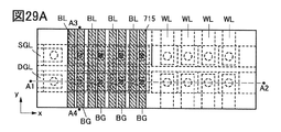
- 29A is a top view illustrating an example of a manufacturing process of a semiconductor device
- FIGS. 29B and 29C are cross-sectional views illustrating an example of a manufacturing process of a semiconductor device.
- 30A is a functional block diagram showing a configuration example of a memory device
- FIG. 30B is a circuit diagram showing a configuration example of a memory string.
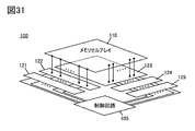
- FIG. 31 is a functional block diagram showing a configuration example of a storage device.
- FIG. 32 is a diagram showing a three-dimensional structural configuration example of a memory cell array.
- FIG. 33 is a diagram showing a three-dimensional structural configuration example of a memory cell array.
- FIG. 34 is a diagram showing a three-dimensional structural configuration example of a memory cell array.
- 35A, 35B, and 35C are circuit diagrams for describing an operation example of the memory device.
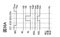
- 36A, 36B, and 36C are timing charts for explaining an operation example of the storage device.
- 37A is a perspective view showing an example of a semiconductor wafer
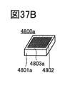
- FIG. 37B is a perspective view showing an example of a chip
- FIGS. 37C and 37D are perspective views showing examples of electronic components.
- 38A, 38B, 38C, 38D, and 38E are schematic diagrams of examples of the storage device.
- FIG. 39 is a block diagram showing a configuration example of an AI system.
- 40A and 40B are block diagrams illustrating application examples of the AI system.
- 41A is a diagram showing an example of an electronic device
- FIG. 41B is a block diagram showing a configuration example of the electronic device.
- 42A, 42B, 42C, 42D, 42E, and 42F are perspective views showing examples of electronic devices.
- the size, the layer thickness, or the region may be exaggerated for clarity. Therefore, it is not necessarily limited to that scale. It should be noted that the drawings schematically show ideal examples and are not limited to the shapes or values shown in the drawings. Further, in the drawings, the same reference numerals are commonly used in different drawings for the same portions or portions having similar functions, and repeated description thereof will be omitted. Further, when referring to the same function, the hatch patterns may be the same and may not be given a reference numeral in particular.
- the ordinal numbers given as the first, second, etc. are used for convenience, and do not indicate the order of steps or the order of stacking. Therefore, for example, the description can be made by appropriately replacing “first” with “second” or “third”.
- the ordinal numbers described in this specification and the like may be different from the ordinal numbers used to specify one embodiment of the present invention.
- the term “electrically connected” includes the case of being connected via “an object having some electrical action”.
- the “object having some kind of electrical action” is not particularly limited as long as it can transfer an electric signal between the connection targets.
- “things having some kind of electrical action” include electrodes and wirings, switching elements such as transistors, resistance elements, inductors, capacitors, and other elements having various functions.
- a nitride oxide refers to a compound in which the content of nitrogen is higher than that of oxygen.
- the oxynitride refers to a compound having a higher oxygen content than nitrogen.
- the content of each element can be measured using, for example, Rutherford backscattering spectroscopy (RBS).
- film and “layer” can be interchanged with each other.
- conductive layer to the term “conductive film”.
- insulating film to the term “insulating layer”.
- parallel means a state in which two straight lines are arranged at an angle of ⁇ 10° or more and 10° or less. Therefore, the case of -5° or more and 5° or less is also included.
- substantially parallel means a state in which two straight lines are arranged at an angle of ⁇ 30° or more and 30° or less.
- vertical means a state in which two straight lines are arranged at an angle of 80° or more and 100° or less. Therefore, the case of 85° or more and 95° or less is also included.
- substantially vertical means a state in which two straight lines are arranged at an angle of 60° or more and 120° or less.
- a crystal when a crystal is a trigonal crystal or a rhombohedral crystal, it is represented as a hexagonal system.
- a barrier film refers to a film having a function of suppressing permeation of impurities such as hydrogen and oxygen, and when the barrier film has conductivity, it is referred to as a conductive barrier film. There is.
- a metal oxide is a metal oxide in a broad sense. Metal oxides are classified into oxide insulators, oxide conductors (including transparent oxide conductors), oxide semiconductors (Oxide Semiconductor or simply OS), and the like. For example, when a metal oxide is used for the active layer of a transistor, the metal oxide may be referred to as an oxide semiconductor.
- FIG. 1 is a cross-sectional view of the memory cell array 700.
- FIG. 2A is a top view of the memory cell array 700. It should be noted that FIG. 2A is a top view of the plane indicated by the alternate long and short dash line of A5-A6 in FIG. 1, and some components are omitted. Further, FIG. 1 is a cross-sectional view of a portion indicated by a dashed-dotted line of A1-A2 in FIG. 2A. Further, FIG.
- FIG. 2B is a cross-sectional view of a portion indicated by an alternate long and short dash line of A3-A4 in FIG. 2A and is a cross-sectional view illustrating an example of the memory string.
- FIG. 3A is an enlarged cross-sectional view of the portion surrounded by the alternate long and short dash line 791 in FIG. 1, and is a diagram illustrating an example of the memory transistor MT functioning as a memory cell.
- FIG. 3B is an enlarged cross-sectional view of the portion surrounded by the alternate long and short dash line 792 in FIG. 1, and is a diagram illustrating an example of a transistor that functions as a selection transistor.
- FIG. 3A is an enlarged cross-sectional view of the portion surrounded by the alternate long and short dash line 791 in FIG. 1, and is a diagram illustrating an example of the memory transistor MT functioning as a memory cell.
- FIG. 3B is an enlarged cross-sectional view of the portion surrounded by the alternate long and short dash line
- a Cartesian coordinate system composed of x-axis, y-axis, and z-axis will be set and described for convenience.
- the x-axis and the y-axis are parallel to the upper surface of the base 720 on which the memory cell array 700 is provided, and the z-axis is vertical to the upper surface of the base 720.
- the memory cell array 700 includes an insulator 721 over a base 720, and a conductor 701 (conductors 701_1 to 701_m:m is a natural number of 2 or more) and an insulator 722 (insulator) on the insulator 721. 722_1 to insulator 722_m) are alternately laminated, a conductor 702 is provided on the laminate, and an insulator 724 is provided on the conductor 702 and the insulator 724.
- An insulator 703 (insulators 703_1 to 703_4) inside the opening formed so as to penetrate the conductor 702, the stacked body, and the insulator 721; and the inside of the insulator 703 is oxidized.
- Object 704 (oxide 704_1 to oxide 704_4), insulator 711 (insulator 711_1 to insulator 711_4) inside the oxide 704, and conductor 712 (conductor 712_1) inside the insulator 711.
- conductors 712_4 and the conductors 705 (conductors 705_1 through 705_4) electrically connected to the upper ends of the oxides 704_1 through 704_4, respectively.
- Conductors 706 (conductors 706_1 to 706_4) that are electrically connected to the lower ends, respectively, and conductors 707 (conductors 707_1 to 707_m) that are electrically connected to the conductors 701_1 to 701_m, respectively.
- a conductor 708 electrically connected to the conductors 707_1 to 707_m (conductors 708_1 to 708_m) and a conductor 709 electrically connected to the conductors 702.
- a conductor 710 electrically connected to the conductor 709, and an insulator 717 and an insulator 713 over the insulator 724, the conductor 705, the conductor 708, and the conductor 710.
- a conductor 714 (illustrated as a conductor 714_1 in FIG. 2B) and a conductor 715 (illustrated as a conductor 715_1 in FIG. 2B) are electrically connected to the conductors 712_1 to 712_4, respectively.
- the conductors 701 are displayed in four or more steps in order to represent the plurality of conductors 701; however, this embodiment is not limited to FIG. It is sufficient that the conductor 701 has two or more stages.
- the conductor 701 is provided so as to extend in the x-axis direction.
- the insulator 703 and the oxide 704 are provided so as to extend in the z-axis direction. That is, the conductor 701, the insulator 703, and the oxide 704 are preferably provided so as to cross each other at right angles.
- the conductor 707 is provided so as to extend in the z-axis direction.
- the conductor 708 may be provided so as to extend in the y-axis direction.
- a conductor functioning as the wiring BL connected to the conductor 705 may be provided by extending in the y-axis direction. Note that part of the conductor 705 may function as the wiring BL and the conductor may be provided so as to extend in the y-axis direction.
- the conductor 712 is formed in a columnar shape, and extends in the z-axis direction. Further, an insulator 711 is provided so as to surround the conductor 712, and an oxide 704 is provided so as to surround the insulator 711, each of which extends in the z-axis direction.
- the conductor 712 is provided like a core inside the columnar oxide 704 extending in the z-axis direction, and the insulator 711 is provided between the oxide 704 and the conductor 712.
- the insulator 703 is provided so as to surround the periphery of the columnar oxide 704.
- the conductor 707 is formed in a columnar shape and is provided so as to extend in the z-axis direction.
- the columnar oxide 704 is electrically connected to the conductor 706 at the lower end in the z-axis direction and is electrically connected to the conductor 705 at the upper end. Further, as shown in FIG. 2B, the conductor 706 is electrically connected to the lower ends of two adjacent columnar oxides 704, and the upper ends of the two columnar oxides 704 are electrically separated from each other. It is electrically connected to the conductor 705.
- a U-shaped memory string in which two columnar oxides 704 are electrically connected by a conductor 706 is described; however, the present invention is not limited to this.
- the conductor 706 may be one of the bit line BL and the source line SL, and the conductor 705 may be the other of the bit line BL and the source line SL.
- the conductor 706 may be electrically connected to the plurality of columnar oxides 704 or may be electrically connected to one columnar oxide 704.
- the conductor 705 may be electrically connected to the plurality of columnar oxides 704 or may be electrically connected to one columnar oxide 704.
- the select transistor is provided near the lower end of the columnar oxide 704 and near the upper end. Is preferably provided.
- the selection transistor SST and the conductor 705 and the memory transistor MT are provided between the conductor 706 and the memory transistor MT.
- a select transistor SDT is provided in between.
- a region where the conductor 701 intersects with the insulator 703 and the oxide 704 and the vicinity thereof function as the memory transistor MT.
- a region where the conductor 702 intersects with the insulator 703 and the oxide 704 and the vicinity thereof function as a selection transistor.
- the channel length directions of these memory transistor MT and select transistor are parallel to the z axis.
- the memory transistor MT and the selection transistor are electrically connected in series to form a memory string.
- FIG. 3A is an enlarged cross-sectional view of the portion surrounded by the alternate long and short dash line 791 in FIG. FIG.
- the memory transistor MT includes the conductor 701_k, the insulator 703 (the insulator 703a, the insulator 703b, and the insulator 703c), and the oxide 704 (the oxide 704a, the oxide 704b, and the oxide 704c). ..
- the memory transistor MT may include the conductor 712 and the insulator 711.
- the conductor 701_k functions as a gate of the memory transistor MT
- the insulator 703a functions as a gate insulating layer
- the insulator 703b functions as a charge storage layer
- the insulator 703c functions as a tunnel insulating layer.
- the oxide 704 includes an oxide 704a, an oxide 704b, and an oxide 704c.
- the oxide 704a has a relatively wide energy gap with respect to the oxide 704b, and thus the oxide 704a has a large energy gap.
- the object 704c has a relatively wide energy gap with respect to the oxide 704b. In other words, the oxide 704b has a relatively narrow energy gap with respect to the oxide 704a and the oxide 704c.
- the oxide 704 included in the k-th memory transistor MT functions as a channel formation region. Further, the oxide 704 between the kth stage memory transistor MT and the k ⁇ 1th stage memory transistor MT, and the oxide 704 between the kth stage memory transistor MT and the k+1th stage memory transistor MT are It is preferable to function as a low resistance region.
- the oxide 704 has a structure in which a channel formation region and a low resistance region are alternately formed, so that series resistance between memory cells can be reduced in a memory string in which memory cells are stacked or a memory cell array. it can.
- the conductor 701_k functions as a first gate and the conductor 712 functions as a second gate.
- the first gate may be simply referred to as a gate or a control gate
- the second gate may be referred to as a back gate.
- An insulator 711 is provided between the oxide 704 and the conductor 712 and functions as a second gate insulating layer.
- the insulator 703a functions as a first gate insulating layer.
- the power consumption of the memory transistor MT can be reduced by controlling the potential of the conductor 712 which functions as the second gate.
- FIG. 3B is an enlarged cross-sectional view of the portion surrounded by the alternate long and short dash line 792 in FIG. 1, showing a cross section of the select transistor (bit line side transistor: SDT and source line side transistor: SST).
- the selection transistor includes the conductor 702, the insulator 703, and the oxide 704 (the oxide 704a, the oxide 704b, and the oxide 704c). Further, the conductor 712 and the insulator 711 may be included.
- the conductor 702 functions as a gate of the selection transistor, and the insulator 703a functions as a gate insulating layer.
- the gate insulating layer may include at least the insulator 703a, and the insulator 703b and the insulator 703c may not be provided. Alternatively, after the insulator 703a, the insulator 703b, and the insulator 703c are provided, the insulator 703b and the insulator 703c may be partially removed.
- the oxide 704 includes the oxide 704a, the oxide 704b, and the oxide 704c.
- the oxide 704a has a relatively wide energy gap with respect to the oxide 704b
- the oxide 704c has the oxide 704b.
- the energy gap is relatively wide.
- the oxide 704b has a relatively narrow energy gap with respect to the oxide 704a and the oxide 704c.
- the conductor 702 functions as a first gate and the conductor 712 functions as a second gate.
- the first gate may be simply called a gate or a top gate, and the second gate may be called a back gate.
- An insulator 711 is provided between the oxide 704 and the conductor 712 and functions as a second gate insulating layer. At this time, the insulator 703a functions as a first gate insulating layer.
- the threshold value of the selection transistor can be controlled by the conductor 712 which functions as the second gate.
- the structure of the semiconductor device described in this embodiment is an example, and the present invention is not limited to the number and arrangement of circuit elements, wirings, and the like shown in the drawings and the like according to this embodiment. ..
- the number, arrangement, and the like of circuit elements and wirings included in the semiconductor device according to this embodiment can be set as appropriate in accordance with the circuit configuration and the driving method.
- the base 720 on which the memory cell array 700 is provided preferably has an insulating surface.
- a semiconductor substrate having an insulator formed on its surface an insulator substrate, a conductor substrate having an insulator formed on its surface, or the like may be used.
- the semiconductor substrate for example, a semiconductor substrate made of any one of silicon and germanium, or any one of silicon carbide, silicon germanium, gallium arsenide, indium phosphide, zinc oxide, gallium oxide, etc.
- a semiconductor substrate or the like may be used.
- a glass substrate for example, a glass substrate, a quartz substrate, a sapphire substrate, a stabilized zirconia substrate (yttria-stabilized zirconia substrate, etc.), a resin substrate, or the like may be used.
- a substrate having an insulator region in the semiconductor substrate described above for example, an SOI (Silicon On Insulator) substrate or the like may be used.
- a graphite substrate, a metal substrate, an alloy substrate, a conductive resin substrate, or the like may be used as the conductor substrate.
- the conductor 701 functions as the gate of the memory transistor MT and is electrically connected to the word line. That is, the conductor 701, the conductor 707, and the conductor 708 also function as part of the word line.
- the conductor 701 is provided in a step shape in which the conductor 701 in the lower layer extends toward the A2 side from the conductor 701 in the upper layer.
- a conductive material such as silicon to which impurities are added or metal can be used.
- silicon is used as the conductor 701
- amorphous silicon, microcrystalline silicon, polycrystalline silicon, single crystal silicon, or the like can be used.
- p-type impurities or n-type impurities may be added in order to give silicon conductivity.
- the conductive material containing silicon silicide containing titanium, cobalt, or nickel can be used as the conductor 701.
- a metal material aluminum, chromium, copper, silver, gold, platinum, tantalum, nickel, titanium, molybdenum, tungsten, hafnium, vanadium, niobium, manganese, magnesium, zirconium, beryllium, indium,
- a material containing one or more metal elements selected from ruthenium and the like can be used.
- the conductor 702 is provided on the conductor 701.
- the conductor 702 functions as a gate of a selection transistor (a selection transistor on the bit line side: SDT and a selection transistor on the source line side: SST) and is electrically connected to the wiring DGL or the wiring SGL. That is, the conductor 702, the conductor 709, and the conductor 710 also function as part of the wiring DGL or the wiring SGL.
- the conductor 702 can be formed using the same material as the conductor 701.
- the conductor 702 may be made of the same material as the conductor 701 or may be made of a different material.
- the conductor 701 and the conductor 702 may be determined in consideration of a work function or the like depending on applications.
- an insulating oxide, a nitride, an oxynitride, a nitride oxide, a metal oxide, a metal oxynitride, or a metal nitriding oxide is used as an insulating film provided in the upper and lower layers of the conductor 701 and the conductor 702.
- a thing etc. can be used.
- silicon oxide, silicon oxynitride, silicon nitride oxide, silicon nitride, fluorine-added silicon oxide, carbon-added silicon oxide, carbon-nitrogen-added silicon oxide, silicon oxide having pores, or resin is Since it has a low dielectric constant, it is suitable for use in the insulating film.
- the insulating film aluminum oxide, gallium oxide, hafnium oxide, zirconium oxide, an oxide containing aluminum and hafnium, an oxynitride containing aluminum and hafnium, an oxide containing silicon and hafnium, and an oxide containing silicon and hafnium It is possible to use a nitride or a nitride containing silicon and hafnium, but since these have a high relative dielectric constant, parasitic capacitance may occur between the conductors 701 or between the conductors 701 and 702. .
- the material used for the insulating film can be determined according to the device design and application.
- the insulator 703 has an insulator 703a, an insulator 703b, and an insulator 703c.
- the insulator 703a is provided on the conductor 701 side
- the insulator 703c is provided on the oxide 704 side
- the insulator 703b is provided between the insulator 703a and the insulator 703c.
- the insulator 703a functions as a gate insulating layer
- the insulator 703b functions as a charge storage layer
- the insulator 703c functions as a tunnel insulating layer.
- the selection transistor may have the same structure as the memory transistor MT.
- the charge storage layer and the tunnel insulating layer may not be provided in the selection transistor.
- the insulator 703b and the insulator 703c may be removed and only the insulator 703a may be provided as the insulator 703.
- the insulator 703b and the insulator 703c may not be provided and only the insulator 703a may be provided as the insulator 703.
- a conductor 712 may be provided as the second gate electrode.
- the conductor 702 functions as a first gate electrode
- the insulator 703a functions as a first gate insulating film
- the insulator 711 functions as a second gate insulating film.
- the conductor 712 can control the threshold value of the selection transistor.
- silicon oxide, silicon oxynitride, or the like it is preferable to use silicon oxide, silicon oxynitride, or the like as the insulator 703a.
- silicon oxide, silicon oxynitride, or the like aluminum oxide, hafnium oxide, zirconium oxide, or an oxide containing two or more selected from aluminum, hafnium, and zirconium may be used. Alternatively, these may be stacked to form the insulator 703a.
- the insulator 703b is preferably made of a material that functions as a charge storage layer, and is preferably made of silicon nitride or silicon nitride oxide. Further, it may have aluminum oxide, hafnium oxide, zirconium oxide, or an oxide containing two or more selected from aluminum, hafnium, and zirconium.
- silicon oxide or silicon oxynitride it is preferable to use silicon oxide or silicon oxynitride as the insulator 703c.
- silicon oxide or silicon oxynitride aluminum oxide, hafnium oxide, zirconium oxide, or an oxide containing two or more selected from aluminum, hafnium, and zirconium may be used. Alternatively, these may be stacked to form the insulator 703c.
- At least one of the insulator 703a, the insulator 703b, and the insulator 703c includes, for example, aluminum oxide, hafnium oxide, tantalum oxide, zirconium oxide, lead zirconate titanate (PZT), strontium titanate (SrTiO 3 ) or An insulator including a so-called high-k material such as (Ba,Sr)TiO 3 (BST) may be used in a single layer or a laminated layer.
- any one of the insulator 703a, the insulator 703b, and the insulator 703c has a stacked structure
- a three-layer stack in which zirconium oxide, aluminum oxide, and zirconium oxide are sequentially formed, or zirconium oxide A four-layer stack in which aluminum oxide, zirconium oxide, and aluminum oxide are sequentially formed may be used.
- a compound containing hafnium and zirconium may be used for at least one of the insulators 703a, 703b, and 703c.
- the insulator 703c functions as a tunnel insulating layer, so that the oxide 704 and the insulator 702b pass through the insulator 703c in the data writing operation or the data erasing operation to the memory transistor MT. In between, charge transfer occurs.
- the insulator 703c in order for the insulator 703c to function as a tunnel insulating layer, the insulator 703c preferably has a smaller thickness than the insulator 703a.
- the insulator 703 formed at the bottom of the opening is formed by dry etching or the like. It must be removed by isotropic etching. During the anisotropic etching, the insulator 703c is also exposed to plasma, radicals, gas, chemical solution, etc., even on the side surface. When the side surface of the insulator 703c is damaged by these, a trap center is generated in the insulator 703c, which might affect the electrical characteristics of the transistor.
- the side surface of the insulator 703c is required to have high resistance to damage due to etching.
- the insulator 703a, the insulator 703b, and the insulator 703c can be formed by an ALD method or a CVD method.
- ALD method atomic layer deposition method
- CVD method vapor deposition method
- exposure to an air atmosphere is performed in the same chamber or by using a multi-chamber deposition apparatus having a plurality of chambers. Instead, it is preferable to form the film continuously.
- oxide 704 it is preferable to use a metal oxide which functions as an oxide semiconductor (hereinafter also referred to as an oxide semiconductor).
- an In-M-Zn oxide (the element M is aluminum, gallium, yttrium, copper, vanadium, beryllium, boron, titanium, iron, nickel, germanium, zirconium, molybdenum, lanthanum, cerium, neodymium).
- the oxide 704 an In—Ga oxide, an In—Zn oxide, an In oxide, or the like may be used.
- the oxide 704 preferably includes an oxide 704a provided on the insulator 703c side, an oxide 704b provided inside the oxide 704a, and an oxide 704c provided inside the oxide 704b.
- the oxide 704a is preferably an oxide having a relatively wide energy gap with respect to the oxide 704b.
- the oxide 704c is preferably an oxide having a relatively wide energy gap with respect to the oxide 704b.
- an oxide having a wide energy gap may be referred to as an oxide having a wide gap and an oxide having a narrow energy gap may be referred to as an oxide having a narrow gap.
- the oxide 704 has a three-layer structure of the oxide 704a, the oxide 704b, and the oxide 704c in FIGS. 3A and 3B, the invention is not limited to this.
- the oxide 704 may have a two-layer structure of the oxide 704a and the oxide 704b, or may have a stacked structure of four or more layers.
- the energy of the bottom of the conduction band of the oxide 704a and the oxide 704c is higher than the energy of the bottom of the conduction band of the oxide 704b. It is preferable that In other words, it is preferable that the electron affinity of the oxide 704a and the oxide 704c be smaller than the electron affinity of the oxide 704b.
- the oxide 704a, the oxide 704b, and the oxide 704c are preferably combined in a different atomic ratio of each metal atom.
- the atomic number ratio of the element M in the constituent elements is the atom of the element M in the constituent element in the metal oxide used for the oxide 704b. It is preferably larger than the number ratio.
- the atomic ratio of the element M to In is preferably higher than the atomic ratio of the element M to In in the metal oxide used for the oxide 704b. ..
- the atomic ratio of In to the element M is preferably higher than the atomic ratio of In to the element M in the metal oxide used for the oxides 704a and 704c. ..
- a metal oxide having a composition of 1, a composition in the vicinity of any one of these, or the like can be used.
- a metal oxide having a composition of 3 to 4.1 and a composition in the vicinity thereof is preferable.
- the above composition indicates the atomic ratio in the oxide formed on the substrate or the atomic ratio in the sputtering target.
- increasing the In ratio as the composition of the oxide 704b is preferable because the on-state current, field-effect mobility, or the like of the transistor can be increased.
- increasing the In ratio of the oxide 704b often results in normally-on transistor characteristics.
- a method for operating a semiconductor device which has favorable normally-on transistor characteristics can be provided. Note that details of a method for operating the semiconductor device of one embodiment of the present invention will be described later.
- normally-on refers to a state in which a channel exists and a current flows through a transistor even when a voltage is not applied to the gate.
- normally-off means that when a potential is not applied to the gate or a ground potential is applied to the gate, the current per channel width of 1 ⁇ m flowing in the transistor is 1 ⁇ 10 ⁇ 20 A or less at room temperature and 85° C. It means 1 ⁇ 10 ⁇ 18 A or less, or 1 ⁇ 10 ⁇ 16 A or less at 125° C.
- CAAC-OS described later be used as the oxide 704a and the oxide 704c and CAC-OS be used as the oxide 704b.
- the c-axis is parallel to the xy plane illustrated in FIGS. 1 and 2, that is, perpendicular to the z-axis and is centered from the side surface of the opening. It is preferably oriented so as to face.
- the bottom of the conduction band changes gently at the junction between the oxide 704a and the oxide 704b and at the junction between the oxide 704c and the oxide 704b.
- the conduction band bottoms at the junction between the oxide 704a and the oxide 704b and the junction between the oxide 704c and the oxide 704b continuously change or continuously join.
- the density of defect states in the mixed layer formed at the interface between the oxide 704a and the oxide 704b and the interface between the oxide 704c and the oxide 704b be low.
- the oxide 704a, the oxide 704b, and the oxide 704c have a common element other than oxygen (as a main component), so that a mixed layer with low defect level density can be formed. it can.
- the oxide 704b is an In—Ga—Zn oxide
- In—Ga—Zn oxide, Ga—Zn oxide, gallium oxide, or the like may be used as the oxide 704a and the oxide 704c.
- the density of defect states in the interface between the oxide 704a and the oxide 704b and the interface between the oxide 704c and the oxide 704b can be reduced. Therefore, the influence of interface scattering on carrier conduction is reduced, and the memory transistor MT can obtain a high on-current.
- oxide 704 Note that a more detailed description of the metal oxide that can be used as the oxide 704 will be described later.
- FIG. 3A is an enlarged view of the memory transistor MT surrounded by the alternate long and short dash line 791 in FIG. As illustrated in FIG. 3A, the oxide 704b is provided so as to be sandwiched between the oxide 704a and the oxide 704c.
- the carrier having a narrow gap is mainly Flowing Therefore, in the case of using the above structure, by sandwiching the oxide 704b having a narrow gap with the oxide 704a having a wide gap and the oxide 704c, carriers flowing in the oxide 704 can be confined in the oxide 704b, In the ON state of the transistor, a high current driving force, that is, a large ON current and a high field effect mobility can be obtained.
- the oxide 704a between the oxide 704b and the insulator 703c the oxide 704b serving as a carrier path is not directly in contact with the insulator 703c, so that formation of a trap center is suppressed.
- the transistor and a semiconductor device including the transistor can have high reliability.
- the metal film, the oxide film containing a metal element, or the nitride film containing a metal element has a property of absorbing hydrogen
- hydrogen in the oxide 704 is It is absorbed into the membrane. Therefore, hydrogen which is an impurity in the oxide 704 can be reduced.
- the metal film, the oxide film containing a metal element, or the nitride film containing a metal element may be removed together with hydrogen absorbed from the oxide 704 in a later step. As a result, the oxide 704 is highly purified (reduction of impurities such as water and hydrogen) and has higher resistance.
- the metal film, the oxide film containing a metal element, or the nitride film containing a metal element does not necessarily have to be removed.
- a metal film, an oxide film containing a metal element, or a nitride film containing a metal element is oxidized by oxygen absorbed from the oxide 704 and becomes an insulator and has high resistance, it may be left. .. In that case, as in the case of the insulator 711, it may function as the second gate insulating layer.
- heat treatment is performed to oxidize the conductive region.
- the metal film, the oxide film containing a metal element, or the nitride film containing a metal element serves as an insulator and has high resistance.
- the heat treatment is preferably performed in an oxidizing atmosphere, for example.
- heat treatment is performed to perform the metal film, the oxide film containing the metal element, or the metal element.
- the nitride film having OH reacts with oxygen contained in the structure and is oxidized.
- the oxide film containing a metal element, or the nitride film containing a metal element can function as a second gate insulating layer similarly to the insulator 711.
- a metal film, an oxide film containing a metal element, or a nitride film containing a metal element is preferably provided with a thickness of 0.5 nm to 5 nm, preferably 1 nm to 2 nm.
- aluminum having a thickness of 0.5 nm to 5 nm is oxidized by heat treatment, aluminum oxide having a thickness of 0.7 nm to 8 nm may be obtained.
- the oxide 704 is in contact with the metal film, the oxide film containing a metal element, or the nitride film containing a metal element in an atmosphere containing nitrogen. It is preferable to perform the heat treatment once. By performing heat treatment once in an atmosphere containing nitrogen, oxygen in the oxide 704 easily diffuses into a metal film, an oxide film containing a metal element, or a nitride film containing a metal element.
- a memory transistor or a selection transistor including an oxide semiconductor when impurities and oxygen vacancies are present in a region where a channel is formed in the oxide semiconductor, electric characteristics are likely to vary and reliability is deteriorated. There is.
- oxygen deficiency when oxygen deficiency is included in a region where a channel is formed in the oxide semiconductor, the transistor is likely to have normally-on characteristics. Therefore, it is preferable that oxygen vacancies in the region where the channel is formed be reduced as much as possible.
- the memory transistor may be operated with normally-on characteristics depending on the specifications of the semiconductor device.
- the same material as the conductor 701 can be used as the conductor 712. Since the conductor 712 needs to be formed inside the opening having a large aspect ratio (in other words, the oxide 704 and the concave portion of the insulator 711), it is formed by a CVD method, an ALD method, or a plating method. It is preferable. At this time, the insulator 711 can be formed using the same material as the insulator 703.
- the insulator 711 is preferably a material that can supply oxygen to the oxide 704.
- oxygen can be supplied to the oxide 704 in some cases.
- the oxide 704 is highly purified.
- the memory transistor MT and the semiconductor device including the memory transistor MT can have high reliability.
- the insulator 711 may be a material capable of supplying impurities such as hydrogen and nitrogen.
- the insulator 711 for example, by using an oxide containing hydrogen or nitrogen, hydrogen or nitrogen can be supplied to the oxide 704 in some cases.
- the resistance value of the oxide 704 may be reduced.
- the memory transistor MT can be operated with a lower driving voltage. Further, in the ON state of the memory transistor MT, a high current drivability, that is, a large ON current and a high field effect mobility can be obtained.
- the opening formed in the stacked body in which the memory transistor MT is provided has an upper surface having a circular shape in FIG. 2A and the like; however, the opening is not limited to this.
- the upper surface may have an elliptical shape, a triangular shape, or a quadrangular shape. It may be a polygonal shape such as. Further, in the case of a polygonal shape, the corners may be rounded.
- the top shapes of the insulator 703 and the oxide 704 may change in accordance with the top shape of the opening. Further, the opening may have a shape in which the cross-sectional area of the opening on the lower side (conductor 706 side) is narrower than that of the opening on the upper side (conductor 705 side).
- the oxide transistor 704, the insulator 703, and the conductor 701 form a memory transistor MT.
- 1 and 2 show an example in which the memory transistors MT are stacked in m stages (m is a natural number of 2 or more). Note that in FIGS. 1 and 2, the conductor 701 is displayed in four or more steps to represent the plurality of conductors 701; however, this embodiment is not limited to FIG. 1 and at least the conductor 701 is illustrated. It suffices to have two or more stages.
- the conductor 705 is electrically connected to the oxide 704 and functions as part of the source line SL or the bit line BL.
- a conductive material containing a metal element is preferably used.
- a material having conductivity can be used among the materials that can be used for the above metal film, the oxide film containing a metal element, or the nitride film containing a metal element. In this case, part of the oxide 704 has low resistance.
- a metal compound layer containing a metal element of the conductor 705 and a component of the oxide 704 is preferably formed at the interface between the conductor 705 and the oxide 704.
- the formation of the metal compound layer is preferable because the contact resistance between the conductor 705 and the oxide 704 is reduced.
- the conductor 705 absorbs oxygen contained in the oxide 704, and the resistance of the oxide 704 near the interface between the conductor 705 and the oxide 704 is reduced, whereby the conductor 705 and the oxide 704 are The contact resistance of can be reduced.
- the conductor 706 is electrically connected to the oxide 704 electrically connected to the conductor 706 functioning as part of the bit line BL and the conductor 705 functioning as part of the source line SL.
- a memory string is formed by electrically connecting the oxide 704 and the oxide 704.
- the area surrounded by the dotted line in FIG. 2A represents a memory string. That is, FIG. 2A shows a memory cell array 700 having four memory strings.
- the same material as the conductor 705 can be used for the conductor 706.
- a material having conductivity can be used among the materials that can be used for the above metal film, the oxide film containing a metal element, or the nitride film containing a metal element. In this case, as described above, part of the oxide 704 has low resistance.
- the conductor 706 may be made of the same material as the conductor 705 or may be made of a different material.
- a metal compound layer containing a metal element of the conductor 706 and a component of the oxide 704 is formed at the interface between the conductor 706 and the oxide 704.
- the formation of the metal compound layer is preferable because the contact resistance between the conductor 706 and the oxide 704 is reduced.
- the conductor 706 absorbs oxygen contained in the oxide 704, and the resistance of the oxide 704 near the interface between the conductor 706 and the oxide 704 is reduced, whereby the conductor 706 and the oxide 704 are The contact resistance of can be reduced.
- a material which can be used for the conductor 701, the conductor 702, or the conductor 712 is used in the same manner. You can The respective conductors may use the same material or different materials.
- FIG. 4 is a top view illustrating a memory cell array 700A in which a plurality of memory cell arrays 700 having six stages of memory transistors MT are combined.
- some components are omitted for ease of explanation.
- the selection transistors bit line side transistor SDT and source line side transistor SST
- the conductor 701 and the conductor 702 that is a component thereof are omitted.
- the conductor 715 that functions as a part of the wiring BG that is electrically connected to the conductor 712 that functions as the second gate is shown by a solid line.
- each memory cell array 700 has four memory strings each having six stages of memory transistors MT.
- the end on the bit line side of the memory string is electrically connected to different bit lines BL (bit lines BL_1 to BL_4).
- bit lines BL_1 to BL_4 bit lines BL_1 to BL_4.
- the end of the memory string on the source line side is electrically connected to the source line SL and is supplied with a common potential.
- the source line SL may be grounded or may be given a constant potential. Further, the potential may be changed according to the operation of the circuit.
- the conductors 701_1 to 701_6 are electrically connected to different word lines WL.
- the conductors 701_1 to 701_6 on the bit line side are electrically connected to the word lines WLa_1 to WLa_6, respectively, and the conductors 701_1 to 701_6 on the source line side are connected to the word lines WLb_1 to WLb_6, respectively. It is electrically connected.
- the conductor 712 included in each memory string is electrically connected to the wiring BG.
- FIG. 4 illustrates an example in which the conductors 712 arranged in the column direction are electrically connected to the common wiring BG, the present invention is not limited to this.
- the conductors 712 arranged in the row direction may be electrically connected to the common wiring BG.
- a different potential may be applied to each wiring BG, or the same potential may be applied to a plurality of wirings BG.
- the plurality of wirings BG are electrically connected to each other.
- the plurality of wirings BG may refer to all the wirings BG included in the memory cell array 700A.
- the wiring BG may be referred to as a circuit which controls the potential of the wiring BG (eg, a BG driver or a BG driver circuit. Further, a driver or a driver). It may be referred to as a circuit)).
- the BG driver circuit may be provided for each wiring BG, or a plurality of wirings BG may be electrically connected to one BG driver circuit.
- the memory cell array 700A may include one BG driver circuit, and all the wirings BG included in the memory cell array 700A may be electrically connected to the BG driver circuit.
- bit line BL bit line BL_1 to bit line BL_4
- word line WLa_1 to word line WLa_6 and word line WLb_1 to word line WLb_6 an arbitrary memory transistor in the memory cell array 700 is selected.
- MT can be selected.
- writing, reading, erasing, and the like can be performed on the selected memory transistor MT.
- a selection transistor (not shown) is provided in each memory string, an arbitrary memory cell array 700 in the memory cell array 700A is selected, and an arbitrary memory transistor MT in the selected memory cell array 700 is selected. Then, writing, reading and erasing can be performed.
- FIG. 5 illustrates a configuration example of a memory device 750 in which the memory cell array 700A is stacked and provided over the circuit 300. As illustrated in FIG. 5, the memory cell array 700A is stacked and provided in a region where the circuit 300 including the transistor 301, the transistor 302, and the transistor 303 is formed. Note that the transistor 301 and the transistor 302 form a sense amplifier 304, and the transistor 303 functions as a column selection switch.
- bit line BL of the memory cell array 700A is electrically connected to one of a source and a drain of the transistor 301, and a gate of the transistor 301 is electrically connected to one of a source and a drain of the transistor 302, The gate of the transistor 302 is electrically connected to the other of the source and the drain of the transistor 301. Further, one of a source and a drain of the transistor 301 and the other of the source and the drain of the transistor 302 are electrically connected to one of a source and a drain of the transistor 303 which functions as a column selection switch. Accordingly, the layout area of the storage device 750 can be reduced. Note that FIG.
- FIG. 5 shows an example in which 10 stages of memory transistors MT are provided and 20 memory transistors MT are provided for each memory string.
- the number of stacked memory transistors MT is not limited to this. For example, 32 layers, 64 layers, 128 layers may be laminated, or 200 layers or more may be laminated.
- the bit line BL of the memory cell array 700A is electrically connected to the sense amplifier 304 and the transistor 303 functioning as a column selection switch through a conductor 752 formed so as to be embedded in an insulator 726, an insulator 722, or the like. Connected.
- the circuits and transistors included in the circuit 300 are examples, and one embodiment of the present invention is not limited to the circuit structure or the transistor structure.
- appropriate circuits and transistors such as a control circuit, a row decoder, a row driver, a source line driver, and an input/output circuit can be provided depending on the structure of the memory device 750 and its driving method.
- the transistor 301, the transistor 302, and the transistor 303 are provided over the substrate 311, and are a conductor 316, an insulator 315, a semiconductor region 313 which is part of the substrate 311, and a low-resistance region functioning as a source region or a drain region, respectively. 314a and a low resistance region 314b. Note that as illustrated in FIG. 5, one low-resistance region may be shared as one source region or drain region and the other source region or drain region of the transistors 301 and 302.
- a semiconductor region 313 (a part of the substrate 311) in which a channel is formed has a convex shape. Further, the side surface and the upper surface of the semiconductor region 313 are provided so as to cover the conductor 316 with the insulator 315 interposed therebetween. Note that the conductor 316 may be formed using a material whose work function is adjusted.
- Such a transistor 301, a transistor 302, and a transistor 303 use a convex portion of a semiconductor substrate, and thus are also called FIN transistors.
- an insulator which functions as a mask for forming the protrusion may be provided in contact with the top of the protrusion.
- the SOI substrate may be processed to form a semiconductor film having a convex shape.
- the transistor 301, the transistor 302, and the transistor 303 may each be a p-channel type or an n-channel type, but the transistor 301 and the transistor 302 are preferably transistors having different polarities.
- a region such as a region where a channel of the semiconductor region 313 is formed, a region in the vicinity thereof, a low resistance region 314a serving as a source region or a drain region, a low resistance region 314b, or the like preferably contains a semiconductor such as a silicon-based semiconductor. It preferably includes crystalline silicon. Alternatively, a material including Ge (germanium), SiGe (silicon germanium), GaAs (gallium arsenide), GaAlAs (gallium aluminum arsenide), or the like may be used. It is also possible to adopt a configuration using silicon in which the effective mass is controlled by applying stress to the crystal lattice and changing the lattice spacing. Alternatively, the transistors 301, 302, and 303 may be HEMTs (High Electron Mobility Transistors) by using GaAs and GaAlAs.
- HEMTs High Electron Mobility Transistors
- the low-resistance region 314a and the low-resistance region 314b impart an n-type conductivity imparting element such as arsenic or phosphorus or a p-type conductivity imparting boron, in addition to the semiconductor material applied to the semiconductor region 313. Including the element to do.
- the insulator 315 functions as a gate insulating film of the transistors 301, 302, and 303.
- the conductor 316 functioning as a gate electrode is a semiconductor material such as silicon, a metal material, or an alloy containing an element imparting n-type conductivity such as arsenic or phosphorus, or an element imparting p-type conductivity such as boron. Materials or conductive materials such as metal oxide materials can be used.
- the work function is determined by the material of the conductor, so the threshold voltage can be adjusted by changing the material of the conductor. Specifically, it is preferable to use a material such as titanium nitride or tantalum nitride for the conductor. Furthermore, in order to achieve both conductivity and embedding properties, it is preferable to use a metal material such as tungsten or aluminum as a laminate for the conductor, and it is particularly preferable to use tungsten in terms of heat resistance.
- an insulator 317 functioning as an etch stopper is provided above the conductor 316.
- an insulator 318 functioning as a spacer is preferably provided on a side surface of the insulator 315.
- the conductor 328 By forming the conductor 328 in the opening formed in this manner, a favorable contact with reduced contact resistance can be obtained between the low resistance region 314a and the low resistance region 314b and the conductor 328.
- the low resistance region 314a thus formed and the contact between the low resistance region 314b and the conductor 328 may be referred to as a self-aligned contact.
- An insulator 320, an insulator 322, an insulator 324, an insulator 326, and an insulator 327 are sequentially stacked to cover the transistor 301, the transistor 302, and the transistor 303.
- the insulator 320, the insulator 322, the insulator 324, the insulator 326, and the insulator 327 for example, silicon oxide, silicon oxynitride, silicon nitride oxide, silicon nitride, aluminum oxide, aluminum oxynitride, aluminum nitride oxide, or nitride is used. Aluminum or the like may be used.
- the insulator 322 may have a function as a flattening film for flattening a step caused by the transistor 301 and the like provided below the insulator 322.
- the upper surface of the insulator 322 may be planarized by a planarization treatment using a chemical mechanical polishing (CMP) method or the like in order to enhance planarity.
- CMP chemical mechanical polishing
- the insulator 324 it is preferable to use a film having a barrier property such that hydrogen and impurities do not diffuse from the substrate 311, the transistor 301, or the like to a region where the memory cell array 700A is provided.
- a film having a barrier property against hydrogen for example, silicon nitride formed by a CVD method can be used.
- silicon nitride formed by a CVD method when hydrogen is diffused into a semiconductor element including an oxide semiconductor, such as the memory transistor MT, characteristics of the semiconductor element may be deteriorated in some cases. Therefore, it is preferable to use a film which suppresses diffusion of hydrogen between the memory transistor MT and the transistor 301 and the like.
- the film that suppresses the diffusion of hydrogen is a film in which the amount of released hydrogen is small.
- the desorption amount of hydrogen can be analyzed by using, for example, a thermal desorption gas analysis method (TDS).
- TDS thermal desorption gas analysis method
- the desorption amount of hydrogen in the insulator 324 is calculated as the desorption amount converted into hydrogen atoms per area of the insulator 324 when the surface temperature of the film is in the range of 50 °C to 500 °C. Therefore, it may be 10 ⁇ 10 15 atoms/cm 2 or less, preferably 5 ⁇ 10 15 atoms/cm 2 or less.
- the insulators 326 and 327 preferably have a lower dielectric constant than the insulator 324.
- the relative permittivity of the insulator 326 and the insulator 327 is preferably less than 4, and more preferably less than 3.
- the relative permittivity of the insulator 326 and the insulator 327 is preferably 0.7 times or less, and more preferably 0.6 times or less that of the insulator 324.
- the insulator 317, the insulator 320, the insulator 322, the insulator 324, the insulator 326, and the insulator 327 include a conductor 328, a conductor 329, a conductor 330, and the like which are electrically connected to the memory cell array 700A. It is embedded. Note that the conductor 328, the conductor 329, and the conductor 330 have a function as a plug or a wiring. The conductor 329 is embedded in the openings of the insulator 317 and the insulator 322, for example, and the conductor 329 is electrically connected to the conductor 316.
- the conductor having a function as a plug or a wiring may have a plurality of structures collectively given the same reference numeral. Further, in this specification and the like, the wiring and the plug electrically connected to the wiring may be integrated. That is, part of the conductor may function as a wiring, and part of the conductor may function as a plug.
- a conductive material such as a metal material, an alloy material, a metal nitride material, or a metal oxide material is used in a single layer or It can be used by stacking. It is preferable to use a high melting point material such as tungsten or molybdenum that has both heat resistance and conductivity, and it is particularly preferable to use tungsten. Alternatively, it is preferably formed of a low resistance conductive material such as aluminum or copper. Wiring resistance can be reduced by using a low-resistance conductive material.
- a wiring layer may be provided on the insulator 327 and the conductor 330.
- an insulator 350, an insulator 352, and an insulator 354 are sequentially stacked and provided.
- a conductor 356 is formed over the insulator 350, the insulator 352, and the insulator 354.
- the conductor 356 has a function as a plug or a wiring. Note that the conductor 356 can be provided using a material similar to that of the conductor 328, the conductor 329, and the conductor 330.
- the insulator 350 is preferably an insulator having a barrier property against hydrogen, like the insulator 324.
- the conductor 356 preferably contains a conductor having a barrier property against hydrogen. That is, it is preferable that the conductor 356 having a barrier property against hydrogen be formed in the opening portion of the insulator 350 having a barrier property against hydrogen.
- tantalum nitride may be used as the conductor having a barrier property against hydrogen.
- tantalum nitride and tungsten having high conductivity diffusion of hydrogen from the transistor 301 or the like can be suppressed while maintaining conductivity as a wiring.
- the tantalum nitride layer having a hydrogen barrier property is in contact with the insulator 350 having a hydrogen barrier property.
- a wiring layer may be provided on the insulator 354 and the conductor 356.
- an insulator 360, an insulator 362, and an insulator 364 are sequentially stacked and provided.
- a conductor 366 is formed over the insulator 360, the insulator 362, and the insulator 364.
- the conductor 366 has a function as a plug or a wiring. Note that the conductor 366 can be provided using a material similar to that of the conductor 328, the conductor 329, and the conductor 330.
- the insulator 360 is preferably an insulator having a barrier property against hydrogen, like the insulator 324.
- the conductor 366 preferably contains a conductor having a barrier property against hydrogen. That is, it is preferable that the conductor 366 having a barrier property against hydrogen be formed in the opening portion of the insulator 360 having a barrier property against hydrogen.
- An insulator 722 is provided on the insulator 364 and the conductor 366, and a memory cell array 700A is provided above the insulator 722.
- a barrier film made of the same material as the insulator 324 may be provided between the insulator 364 and the insulator 722.
- FIG. 5 shows an example of a memory cell array 700A having a U-shaped memory string in which two columnar oxides 704 are electrically connected by a conductor 706, but the present invention is not limited to this.
- FIG. 6 shows a columnar oxide 704 having an eight-stage memory transistor MT and two selection transistors (SDT, SST), and the lower end of one columnar oxide 704 is a conductor 705B that functions as a bit line BL. In this example, the upper end is electrically connected to the conductor 705S that functions as the source line SL. That is, one columnar oxide 704 constitutes one memory string.
- the conductor 705B is electrically connected to the lower ends of the four columnar oxides, but the present invention is not limited to this.
- One conductor 705B may be electrically connected to one columnar oxide 704, or one conductor 705B may be electrically connected to two or more columnar oxides 704. Further, the conductor 705S is electrically connected to the upper ends of the two columnar oxides, but the present invention is not limited to this. One conductor 705S may be electrically connected to one columnar oxide 704, or one conductor 705S may be electrically connected to two or more columnar oxides 704.
- a selection transistor SDT is provided between the conductor 705B and the memory transistor MT, and a selection transistor SST is provided between the conductor 705S and the memory transistor MT. Since the conductor 705B functioning as the bit line BL is electrically connected to the circuit 300 provided therebelow, a wiring (routing wiring) or a plug for electrically connecting the memory cell array 700A and the circuit 300 can be formed. This is preferable because the number can be reduced and the layout area of the memory device 750 can be further reduced.
- the stacked memory transistors MT have eight stages in FIG. 6, the present invention is not limited to this. The number of stages may be 2 or more and 7 or less, or 9 or more. For example, 32 layers, 64 layers, 128 layers may be laminated, or 200 layers or more may be laminated.
- metal oxides applicable to the oxide 704 according to the present invention will be described.
- the metal oxide preferably contains at least indium or zinc. It is particularly preferable to contain indium and zinc. In addition to these, it is preferable that aluminum, gallium, yttrium, tin, or the like is contained. Further, one or more selected from boron, titanium, iron, nickel, germanium, zirconium, molybdenum, lanthanum, cerium, neodymium, hafnium, tantalum, tungsten, magnesium or the like may be contained.
- the metal oxide is an In-M-Zn oxide containing indium, the element M, and zinc.
- the element M is aluminum, gallium, yttrium, tin, or the like.
- Other elements applicable to the element M include boron, titanium, iron, nickel, germanium, zirconium, molybdenum, lanthanum, cerium, neodymium, hafnium, tantalum, tungsten and magnesium.
- the element M it may be acceptable to combine a plurality of the aforementioned elements.
- metal oxides containing nitrogen may be collectively referred to as metal oxides. Further, the metal oxide containing nitrogen may be referred to as a metal oxynitride.
- CAC-OS or CAC-metal oxide has a conductive function in a part of the material and an insulating function in a part of the material, and the whole material has a function as a semiconductor.
- the conductive function is a function of flowing electrons (or holes) serving as carriers
- the insulating function is carrier. It is a function that does not flow electrons.
- the CAC-OS or the CAC-metal oxide has a conductive area and an insulating area.
- the conductive region has the above-mentioned conductive function
- the insulating region has the above-mentioned insulating function.
- the conductive region and the insulating region may be separated at the nanoparticle level.
- the conductive region and the insulating region may be unevenly distributed in the material.
- the conductive region may be observed by blurring the periphery and connecting in a cloud shape.
- the conductive region and the insulating region are dispersed in the material in a size of 0.5 nm or more and 10 nm or less, preferably 0.5 nm or more and 3 nm or less. There is.
- CAC-OS or CAC-metal oxide is composed of components having different band gaps.
- CAC-OS or CAC-metal oxide is composed of a component having a wide gap due to the insulating region and a component having a narrow gap due to the conductive region.
- the carrier when the carrier flows, the carrier mainly flows in the component having the narrow gap.
- the component having the narrow gap acts complementarily to the component having the wide gap, and the carrier also flows in the component having the wide gap in conjunction with the component having the narrow gap. Therefore, when the CAC-OS or CAC-metal oxide is used in the channel formation region of the transistor, a high current driving force, that is, a high on-current and a high field-effect mobility can be obtained in the on state of the transistor.
- CAC-OS or CAC-metal oxide can also be referred to as a matrix composite material or a metal matrix composite material.
- the oxide semiconductor (metal oxide) is classified into a single crystal oxide semiconductor and a non-single crystal oxide semiconductor other than the single crystal oxide semiconductor.
- the non-single-crystal oxide semiconductor include a CAAC-OS (c-axis aligned crystal oxide semiconductor), a polycrystalline oxide semiconductor, a nc-OS (nanocrystal oxide semiconductor), and a pseudo-amorphous oxide semiconductor (a-like oxide).
- OS amorphous-like oxide semiconductor (OS) and amorphous oxide semiconductors.
- FIG. 7A is a diagram illustrating classification of crystal structures of oxide semiconductors, typically IGZO (a metal oxide containing In, Ga, and Zn).
- IGZO a metal oxide containing In, Ga, and Zn
- IGZO is roughly classified into Amorphous, Crystalline, and Crystal. Moreover, completeness amorphous is included in Amorphous.
- CAAC c-axis aligned crystalline
- nc nanocrystalline
- CAC Cloud-Aligned Composite
- single crystal and poly crystal are included in Crystal.
- the structure in the thick frame shown in FIG. 7A belongs to the New crystalline phase.
- the structure is in the boundary region between Amorphous and Crystal. That is, it can be said that the energy-unstable Amorphous and Crystalline are completely different structures.
- the crystal structure of the film or substrate can be evaluated using an X-ray diffraction (XRD: X-Ray Diffraction) image.
- XRD X-ray diffraction
- FIGS. 7B and 7C XRD spectra of quartz glass and IGZO (also referred to as crystalline IGZO) having a crystal structure classified into Crystalline are shown in FIGS. 7B and 7C.
- FIG. 7B is a quartz glass
- FIG. 7C is an XRD spectrum of crystalline IGZO.
- the crystalline IGZO shown in FIG. 7C has a thickness of 500 nm.
- the peak of the XRD spectrum of quartz glass is almost symmetrical.
- crystalline IGZO has an asymmetric peak in the XRD spectrum.
- the asymmetric peak in the XRD spectrum is evidence of the presence of crystals. In other words, unless the peak of the XRD spectrum is symmetrical, it cannot be said to be Amorphous.
- CAAC-OS has a crystal structure having c-axis orientation and a plurality of nanocrystals connected in the ab plane direction and having strain.
- the strain refers to a portion in which the orientation of the lattice arrangement is changed between a region where the lattice arrangement is uniform and another region where the lattice arrangement is uniform in the region where the plurality of nanocrystals are connected.
- Nanocrystals are basically hexagonal, but they are not limited to regular hexagons and may be non-regular hexagons.
- the strain may have a lattice arrangement such as a pentagon and a heptagon.
- a lattice arrangement such as a pentagon and a heptagon.
- the CAAC-OS is a layered crystal in which a layer containing indium and oxygen (hereinafter, an In layer) and a layer containing elements M, zinc, and oxygen (hereinafter, a (M,Zn) layer) are stacked. It tends to have a structure (also called a layered structure). Note that indium and the element M can be replaced with each other, and when the element M of the (M,Zn) layer is replaced with indium, it can be expressed as an (In,M,Zn) layer. When the indium in the In layer is replaced with the element M, it can be expressed as an (In,M) layer.
- CAAC-OS is a metal oxide with high crystallinity.
- CAAC-OS since it is difficult to confirm a clear crystal grain boundary, it can be said that a decrease in electron mobility due to the crystal grain boundary does not easily occur.
- CAAC-OS impurities and defects oxygen deficiency (V O: also referred to as oxygen vacancy), etc.) with little metal oxide It can be called a thing. Therefore, the metal oxide having CAAC-OS has stable physical properties. Therefore, the metal oxide containing CAAC-OS is highly heat resistant and highly reliable.
- Nc-OS has a periodic atomic arrangement in a minute region (for example, a region of 1 nm or more and 10 nm or less, particularly a region of 1 nm or more and 3 nm or less). Moreover, in the nc-OS, no regularity is found in the crystal orientation between different nanocrystals. Therefore, no orientation is seen in the entire film. Therefore, the nc-OS may be indistinguishable from the a-like OS or the amorphous oxide semiconductor depending on the analysis method.
- the a-like OS is a metal oxide having a structure between the nc-OS and the amorphous oxide semiconductor.
- the a-like OS has a void or a low density region. That is, the crystallinity of the a-like OS is lower than that of the nc-OS and the CAAC-OS.
- Oxide semiconductors have various structures, and each has different characteristics.
- the oxide semiconductor of one embodiment of the present invention may include two or more of an amorphous oxide semiconductor, a polycrystalline oxide semiconductor, an a-like OS, an nc-OS, and a CAAC-OS.
- ⁇ Electrical conduction in solids is hindered by a scattering source called scattering center.
- scattering center a scattering source
- lattice scattering and ionized impurity scattering are the main scattering centers.
- excess oxygen exists in a metal compound containing more oxygen than the stoichiometric composition.
- Excess oxygen existing in a free state in the metal compound becomes O ⁇ or O 2 ⁇ by receiving an electron.
- Excess oxygen that has become O ⁇ or O 2 ⁇ may become a scattering center.
- the carrier mobility is high when the metal oxide has an essential state containing oxygen satisfying the stoichiometric composition.
- Indium-gallium-zinc oxide which is a kind of metal oxide containing indium, gallium, and zinc, tends to have difficulty in crystal growth especially in the air, and thus has a large crystal structure. It may be structurally more stable to use a crystal (for example, the above-described nanocrystal) smaller than (here, a crystal of several mm or a crystal of several cm). It is considered that the strain energy is relaxed when the small crystals are connected to each other rather than when the large crystals are formed.
- IGZO Indium-gallium-zinc oxide
- defects may be formed in the region where small crystals are connected to each other in order to relax the strain energy in the region. Therefore, the mobility of carriers can be increased by relaxing strain energy without forming defects in the region.
- a metal oxide having a low carrier concentration is preferably used for the transistor.
- the impurity concentration in the metal oxide film may be lowered and the defect level density may be lowered.
- low impurity concentration and low defect level density are referred to as high-purity intrinsic or substantially high-purity intrinsic.
- the metal oxide preferably has a carrier concentration of less than 1 ⁇ 10 18 cm ⁇ 3 , more preferably less than 1 ⁇ 10 17 cm ⁇ 3, and less than 1 ⁇ 10 16 cm ⁇ 3. Is more preferable, less than 1 ⁇ 10 13 cm ⁇ 3 is more preferable, and less than 1 ⁇ 10 12 cm ⁇ 3 is further preferable.
- the lower limit of the carrier concentration of the metal oxide in the channel formation region is not particularly limited, but can be set to, for example, 1 ⁇ 10 ⁇ 9 cm ⁇ 3 .
- the trap level density may be low.
- the charge trapped in the trap level of the metal oxide takes a long time to disappear and may behave as if it were a fixed charge. Therefore, a transistor including a metal oxide having a high trap level density in a channel formation region may have unstable electrical characteristics.
- Impurities include hydrogen, nitrogen, alkali metals, alkaline earth metals, iron, nickel, silicon and the like.
- the concentration of silicon or carbon in the metal oxide and the concentration of silicon or carbon in the vicinity of the interface with the metal oxide are 2). It is not more than ⁇ 10 18 atoms/cm 3 , preferably not more than 2 ⁇ 10 17 atoms/cm 3 .
- the metal oxide contains an alkali metal or an alkaline earth metal
- a defect level may be formed and a carrier may be generated. Therefore, a transistor including a metal oxide containing an alkali metal or an alkaline earth metal in a channel formation region is likely to have normally-on characteristics. Therefore, it is preferable to reduce the concentration of alkali metal or alkaline earth metal in the metal oxide.
- the concentration of alkali metal or alkaline earth metal in the metal oxide obtained by SIMS is set to 1 ⁇ 10 18 atoms/cm 3 or less, preferably 2 ⁇ 10 16 atoms/cm 3 or less.
- the nitrogen in the channel formation region is preferably reduced as much as possible.
- the nitrogen concentration in the metal oxide is less than 5 ⁇ 10 19 atoms/cm 3 in SIMS, preferably 5 ⁇ 10 18 atoms/cm 3 or less, more preferably 1 ⁇ 10 18 atoms/cm 3 or less, and further It is preferably 5 ⁇ 10 17 atoms/cm 3 or less.
- the metal oxide reacts with oxygen bonded to a metal atom to be water, which might cause oxygen deficiency. When hydrogen enters the oxygen vacancies, electrons which are carriers may be generated. Further, part of hydrogen may be bonded to oxygen which is bonded to a metal atom to generate an electron which is a carrier. Therefore, a transistor including a metal oxide containing hydrogen is likely to have normally-on characteristics. Therefore, it is preferable that hydrogen in the metal oxide be reduced as much as possible.
- the hydrogen concentration obtained by SIMS is less than 1 ⁇ 10 20 atoms/cm 3 , preferably less than 1 ⁇ 10 19 atoms/cm 3 , and more preferably 5 ⁇ 10 18 atoms/cm 3. It is less than 3 , and more preferably less than 1 ⁇ 10 18 atoms/cm 3 .
- the off-state current of the transistor can be reduced and stable electrical characteristics can be imparted.
- FIGS. 8 to 12 are cross-sectional views showing a manufacturing process of the memory transistor MT.
- conductors 701 and insulators 722 are alternately laminated.
- the conductor 701 and the insulator 722 are processed to form an opening having a diameter of ⁇ 1 in the conductor 701 and the insulator 722.
- an insulator 703 and an oxide 704 are formed inside the opening having a diameter of ⁇ 1.
- the insulator 703 is formed by sequentially stacking an insulator 703a, an insulator 703b, and an insulator 703c.
- the oxide 704 is formed by sequentially stacking the oxide 704a, the oxide 704b, and the oxide 704c.
- the insulator 703 at the bottom of the opening is preferably removed before the oxide 704 is formed.
- the insulator 703a is formed with high coating property so as to be in contact with the side surface of the conductor 701 and the side surface of the insulator 722.
- the oxide 704 when the oxide 704 is formed inside the opening having the diameter of ⁇ 1, the oxide 704 may be formed thicker than the side surface of the opening on the conductor 706 at the bottom of the opening, as shown in FIG. 9B. is there.
- a reverse sputtering process may be used after forming the oxide 704.
- the reverse sputtering treatment refers to treatment for applying a voltage to the substrate side with use of an RF (Radio Frequency) power source to form plasma in the vicinity of the substrate to modify the surface.
- RF Radio Frequency
- the film 718 may be formed so as to be in contact with the oxide 704 as illustrated in FIG. 10A.
- a film having a property of absorbing hydrogen may be used as the film 718.
- a film having a property of supplying impurities such as hydrogen and nitrogen as the film 718 for example, a metal film, an oxide film containing a metal element, a nitride film containing a metal element, or the like
- heat treatment may be performed if necessary.
- the film 718 may be removed as illustrated in FIG. 10B.
- the heat treatment for example, after the insulator 721 and the insulator 726 are formed and before the insulator 717 is formed, the heat treatment can be performed so that impurities (typically, impurities) contained in the oxide 704 can be formed. Water or hydrogen) can be removed.
- the heat treatment may be performed after forming the insulator 721, the insulator 726, and the insulator 717, or both before and after forming the insulator 717, for example.
- the insulator 721, the insulator 726, and the insulator 717 preferably have a structure in which aluminum oxide and silicon nitride are combined.
- aluminum oxide has a function of capturing hydrogen or fixing hydrogen.
- silicon nitride has a function of having a high blocking property against hydrogen.
- hydrogen can be efficiently removed. Specifically, for example, when silicon nitride having a high blocking property against hydrogen is used as the insulator 703b included in the insulator 703, hydrogen contained in the oxide 704 diffuses into the insulator 703c and the insulator 711. , Reaches the insulator 717.
- the insulator 717 can capture or fix hydrogen diffused from the oxide 704 to the insulator 703c and the insulator 711. it can. Further, for example, in the case where the insulator 703 does not have a blocking property against hydrogen, hydrogen is efficiently extracted from the oxide 704 by using a structure in which the insulator 721 and the insulator 726 are combined with aluminum oxide and silicon nitride. be able to. Further, the insulator 721 preferably contains excess oxygen.
- hydrogen existing in the oxide 704 diffuses to another structure through the insulator 703c, the insulator 711, and the insulator 717 which are in contact with the oxide 704. Specifically, excess oxygen in the insulator 703c and the insulator 711 reacts with hydrogen of the oxide 704 to form an OH bond, and the hydrogen atom diffuses in the insulator 703c and the insulator 711.
- a material having a function of trapping or fixing hydrogen eg, aluminum oxide
- it reacts with an oxygen atom bonded to a metal atom in aluminum oxide to form an insulator 717. May be trapped or stuck inside.
- a hydrogen atom having an OH bond which is not captured or fixed in the insulator 717 may diffuse to the insulator 722, the insulator 724, or the like through the insulator 703.
- hydrogen permeates the insulator 722 and the insulator 724 and is captured or fixed to the insulator 726.
- the oxygen atom of the excess oxygen having an OH bond remains in the insulator 703c and the insulator 711 as excess oxygen. That is, in diffusion of the hydrogen, the excess oxygen in the insulator 703c and the insulator 711 is likely to play a bridging role.
- the heat treatment is preferably performed at a temperature of 350° C. or higher, preferably 400° C. or higher, in an atmosphere containing oxygen, an atmosphere containing nitrogen, or a mixed atmosphere of oxygen and nitrogen.
- the heat treatment time is 1 hour or longer, preferably 4 hours or longer, and more preferably 8 hours or longer.
- the film 718 does not necessarily have to be removed.
- the film 718 when the film 718 is an insulator or is oxidized by oxygen absorbed from the oxide 704 and becomes an insulator, the film 718 may be left. In that case, as in the case of the insulator 711, it may function as the second gate insulating layer.
- the film 718 has at least one of a function of supplying hydrogen to the oxide 704, a function of supplying nitrogen to the oxide 704, and a function of extracting oxygen from the oxide 704. Is preferred.
- the film 718 having such a function is in contact with the oxide 704, carriers are generated in the oxide 704.
- the oxygen deficiency occurs in the oxide 704 by extracting oxygen from the oxide 704.
- Carriers are generated by trapping hydrogen in the oxygen deficiency.
- nitrogen is trapped in the generated oxygen vacancies, oxygen and nitrogen which are bonded to two indium atoms are replaced.
- nitrogen is bonded to these two indium atoms, nitrogen has an unpaired electron and is considered to function as a carrier.
- silicon nitride containing hydrogen As a material having a function of supplying hydrogen to the oxide 704, silicon nitride containing hydrogen can be used. A material formed using a gas containing hydrogen can be used at the time of formation, and silicon, silicon oxide, silicon oxynitride, silicon nitride oxide, or the like formed using monosilane, disilane, ammonia, or the like can be used. You can As a material having a function of supplying nitrogen to the oxide 704, a nitride containing silicon or a metal element can be used. As such a material, silicon nitride, silicon nitride oxide, silicon oxynitride, or the like can be used.
- a nitride containing one or more of aluminum, tantalum, and titanium can be used.
- aluminum nitride, tantalum nitride, titanium nitride, a nitride containing aluminum and tantalum, a nitride containing aluminum and titanium, or the like can be used.
- the film 718 is preferably provided with a thickness of 0.5 nm to 5 nm, preferably 1 nm to 2 nm.
- aluminum having a thickness of 0.5 nm to 5 nm is oxidized by heat treatment, aluminum oxide having a thickness of 0.7 nm to 8 nm may be obtained.
- the oxide 704 is in contact with the metal film, the oxide film containing a metal element, or the nitride film containing a metal element in an atmosphere containing nitrogen. It is preferable to perform the heat treatment once. By performing heat treatment once in an atmosphere containing nitrogen, oxygen in the oxide 704 easily diffuses into a metal film, an oxide film containing a metal element, or a nitride film containing a metal element.
- heat treatment is preferably performed.
- extraction of oxygen, supply of hydrogen, or supply of nitrogen is promoted, so that the resistance of the oxide 704 can be efficiently reduced.
- an insulator 711 is formed inside the oxide 704, and a conductor 712 is formed inside the insulator 711 (see FIG. 11A). Note that when the film 718 is not removed in the previous step, the film 718 may be treated as the insulator 711, or the insulator 711 may be formed inside the film 718.
- 11B is an enlarged view of a portion surrounded by a dashed-dotted line in FIG.
- 11A including a conductor 701_k-1 at the k ⁇ 1th stage, an insulator 722_k ⁇ 1, a conductor 701_k at the kth stage, and A cross section of an insulator 722_k and a conductor 701_k+1 (k is an integer of 2 or more and m-1 or less) at the (k+1)th stage is illustrated.
- the region 734 of the oxide 704 functions as a channel formation region of the memory transistor MT located in the kth stage.
- the region 731a functions as one of the source and the drain of the memory transistor MT located in the kth stage, and the region 731b functions as the other of the source and the drain of the memory transistor MT located in the kth stage.
- the conductor 701_k functions as a first gate of the memory transistor MT located in the kth stage, the conductor 712 functions as a second gate, and the insulator 703a functions as a first gate insulating layer.
- the insulator 703b functions as a charge storage layer
- the insulator 703c functions as a tunnel insulating layer
- the insulator 711 functions as a second gate insulating layer.
- the source or drain of the memory transistor MT including the conductor 701_k as a gate might function as a drain or a source in a transistor positioned above and below.
- the region 731b may function as the drain of the transistor whose gate is the conductor 701_k+1.
- the region 732a and the region 732b may function as a channel formation region similarly to the region 734, or may function as a source or a drain similarly to the region 731a and the region 731b.
- the memory transistor MT that functions as a memory cell can be formed through the above steps.
- the memory cell array is manufactured by the above method, even if the number of layers of the memory transistor MT is increased, the number of steps of pattern formation and etching processing of the memory transistor MT does not increase.
- the steps of manufacturing the memory cell array can be shortened, a semiconductor device with high productivity can be provided.
- FIG. 12 is a diagram showing a different example of the conductor 701.
- the conductor 701 has a three-layer structure of a conductor 701a, a conductor 701b, and a conductor 701c. With such a shape, an electric field from the conductor 701 can be applied not only to the region 734 but also to the region 732, which is preferable because the on characteristics of the memory transistor MT are improved.
- FIGS. 13 to 29 A in each drawing is a top view seen from the z-axis direction, and B in each drawing is a cross-sectional view of a portion indicated by a dashed line A1-A2 in the corresponding A drawing. Is.
- C in each drawing is a cross-sectional view of a portion indicated by a chain line of A3-A4 in the corresponding A drawing.
- FIG. 22D is an enlarged cross-sectional view of the portion surrounded by the alternate long and short dash line in FIG. 22B.
- the conductor 706 is formed over the base 720 having an insulating surface, and the insulator 721 is formed so as to cover the conductor 706 (see FIGS. 13A to 13C).
- a conductive film is formed, and the conductive film is processed by a lithography method to form a conductor 706.
- the method for forming the conductor 706 and the insulator 721 is not limited to this.
- the insulator 721 may be formed over the base 720, and an unnecessary portion of the insulator 721 may be removed to form a groove or an opening, and the conductor 706 may be embedded in the groove or the opening. ..
- Such a method of forming a conductor may be called a damascene method (single damascene method, dual damascene method).
- the conductor 706 and the insulator 721 are formed by a sputtering method, a chemical vapor deposition (CVD) method, a molecular beam epitaxy (MBE) method, a pulsed laser deposition (PLD: Pulsed Laser Deposition) method. Method or ALD (Atomic Layer Deposition) method or the like.
- the CVD method can be classified into a plasma CVD method using plasma (PECVD: Plasma Enhanced CVD) method, a thermal CVD method using heat (TCVD: Thermal CVD) method, an optical CVD method using light (Photo CVD) method, and the like. .. Further, it can be divided into a metal CVD (MCVD: Metal CVD) method and a metal organic CVD (MOCVD: Metal Organic CVD) method depending on the raw material gas used.
- PECVD Plasma Enhanced CVD
- TCVD Thermal CVD
- Photo CVD optical CVD method using light
- MCVD Metal CVD
- MOCVD Metal Organic CVD
- the plasma CVD method can obtain a high quality film at a relatively low temperature.
- the thermal CVD method is a film forming method which can reduce plasma damage to an object to be processed because plasma is not used.
- a wiring, an electrode, an element (a transistor, a capacitor, or the like) included in a semiconductor device might be charged up by receiving electric charge from plasma. At this time, the accumulated charges may destroy wirings, electrodes, elements, and the like included in the semiconductor device.
- a thermal CVD method that does not use plasma, such plasma damage does not occur, so that the yield of semiconductor devices can be increased.
- the thermal CVD method since plasma damage does not occur during film formation, a film with few defects can be obtained.
- the ALD method is a film forming method that can reduce plasma damage to an object to be processed. Also in the ALD method, plasma damage does not occur during film formation, and thus a film with few defects can be obtained.
- the CVD method and the ALD method are film forming methods in which a film is formed by a reaction on the surface of an object to be processed, unlike the film forming method in which particles emitted from a target or the like are deposited. Therefore, the film forming method is not easily affected by the shape of the object to be processed and has a good step coverage.
- the ALD method since the ALD method has excellent step coverage and excellent thickness uniformity, it is suitable for coating the surface of the opening having a high aspect ratio.
- the ALD method has a relatively low film forming rate, it may be preferable to use it in combination with another film forming method such as a CVD method having a high film forming rate.
- the composition of the obtained film can be controlled by the flow rate ratio of the source gas.
- a film having an arbitrary composition can be formed depending on the flow rate ratio of the source gas.
- a film whose composition is continuously changed can be formed by changing the flow rate ratio of the source gas during film formation.
- the resist is exposed through a photomask.
- the exposed area is removed or left with a developing solution to form a resist mask.
- the conductor, the semiconductor, the insulator, or the like can be processed into a desired shape by etching through the resist mask.
- the resist mask may be formed by exposing the resist using KrF excimer laser light, ArF excimer laser light, EUV (Extreme Ultraviolet) light, or the like.
- an immersion technique may be used in which a liquid (for example, water) is filled between the substrate and the projection lens to perform exposure.
- an electron beam or an ion beam may be used instead of the above-mentioned light.
- the resist mask can be removed by dry etching treatment such as ashing, wet etching treatment, wet etching treatment after dry etching treatment, or dry etching treatment after wet etching treatment.
- a hard mask made of an insulator or a conductor may be used instead of the resist mask.
- a hard mask an insulating film or a conductive film to be a hard mask material is formed on a conductive film, a resist mask is formed thereon, and the hard mask material is etched to form a hard mask having a desired shape. be able to.
- the dry etching method and the wet etching method can be used for the processing. Processing by the dry etching method is suitable for fine processing.
- a capacitively coupled plasma (CCP) etching device having parallel plate electrodes can be used as a dry etching device.
- the capacitively coupled plasma etching apparatus having the parallel plate electrodes may have a configuration in which a high frequency power source is applied to one of the parallel plate electrodes.
- a plurality of different high frequency power supplies may be applied to one of the parallel plate electrodes.
- a high frequency power source having the same frequency may be applied to each of the parallel plate electrodes.
- a configuration may be adopted in which high frequency power supplies having different frequencies are applied to the parallel plate electrodes.
- a dry etching apparatus having a high density plasma source can be used.
- an inductively coupled plasma (ICP: Inductively Coupled Plasma) etching apparatus can be used as a dry etching apparatus having a high-density plasma source.
- the etching process may be performed after removing the resist mask used for forming the hard mask, or may be performed with the resist mask left. In the latter case, the resist mask may disappear during etching. After etching the conductive film, the hard mask may be removed by etching. On the other hand, if the material of the hard mask does not affect the post-process or can be used in the post-process, it is not always necessary to remove the hard mask.
- a conductive film containing a metal element is preferably formed by a sputtering method. Alternatively, it can be formed by a CVD method.
- the surface of the insulator 721 is preferably flattened as necessary.
- a chemical mechanical polishing (CMP) method or a reflow method can be used for the flattening treatment.
- the conductive film 701A and the insulating film 722A are alternately stacked over the conductor 706 and the insulator 721 (see FIGS. 14A to 14C).
- this embodiment mode shows an example in which the conductive film 701A is formed over the insulator 721 and the insulating film 722A is formed over the conductive film 701A, the order of formation is not limited to this.
- the insulating film 722A may be formed over the insulator 721 and the conductive film 701A may be formed over the insulating film 722A.
- a CVD method can be used for forming the conductive film 701A and the insulating film 722A.
- a sputtering method may be used.
- the number of stacked layers is not limited to this. Five or more layers may be formed for each, depending on the required performance of the semiconductor device.
- the conductive film 701A and the insulating film 722A may be formed in 32 layers, 64 layers, 128 layers, or 200 layers or more, respectively.
- a conductive film 702A is formed on the uppermost insulating film 722A.
- a mask 723 is formed over the conductive film 702A (see FIGS. 14A to 14C).
- the conductive film 702A can be formed using a method similar to that of the conductive film 701A and a similar material. Note that the conductive film 702A may be formed by the same method as the conductive film 701A or may be formed by a different method. The conductive film 702A may be the same material as the conductive film 701A or may be a different material.
- the conductive film 702A, the conductive film 701A, and the insulating film 722A are processed to form a step-like conductive film 701B, a conductive film 702B, and an insulating film 722B as shown in FIG. 15B.
- etching of the conductive film 702A, the conductive film 701A, and the insulating film 722A and slimming of the mask 723 are alternately performed, so that the step-shaped conductive film 701B, The conductive film 702B and the insulating film 722B can be formed.
- the mask 723 is reduced in both width and thickness to be a mask 723A (see FIGS. 15A to 15C).
- the insulator 724 can be formed by a CVD method.
- the insulator 724 is preferably planarized by a CMP method or a reflow method.
- a mask 725 is formed over the insulator 724. By forming the mask 725 over the planarized insulator 724, lithography accuracy is improved (see FIGS. 16A to 16C).
- the insulator 724, the conductive film 702B, the conductive film 701B, the insulating film 722B, and the insulator 721 are processed using the mask 725.
- a conductor 701 that functions as a gate of the memory transistor MT and is electrically connected to a word line and a conductor 702 that functions as a gate of a selection transistor are formed.
- the insulating film 722B becomes the insulator 722 by the processing (see FIGS. 17A to 17C).
- the mask 725 is removed.
- the insulator 726 is formed so as to fill the portions of the insulator 724, the conductive film 702B, the conductive film 701B, the insulating film 722B, and the insulator 721, which are removed by the above processing.
- the insulator 726 can be formed by a CVD method or an ALD method.
- a film having a uniform thickness can be formed even in a groove or an opening having a large aspect ratio, which is preferable.
- the insulator 726 may be formed by combining the ALD method and the CVD method.
- the insulator 726 is preferably planarized by a CMP method or a reflow method.
- the insulator 726 may be polished until the surface of the insulator 724 is exposed. Further, the insulator 724 and the insulator 726 may be polished together. In this case, the insulator 724 is thin.
- the insulator 724 is processed by a lithography method to form a first opening so that the conductor 701 and the conductor 702 are exposed.
- the first opening is formed in each of the conductors 701 formed in a step shape (see FIGS. 18A to 18C).
- a conductor 707 electrically connected to the conductor 701 and a conductor 709 electrically connected to the conductor 702 are formed so as to be embedded in the first opening (see FIGS. 19A to 19C). ..
- the conductor 707 and the conductor 709 can be formed by a CVD method or an ALD method.
- a film having a uniform thickness can be formed even in a groove or an opening having a large aspect ratio, which is preferable.
- the conductor 707 and the conductor 709 may be formed by combining the ALD method and the CVD method.
- the conductor 707 and the conductor 709 may have a stacked structure including a plurality of layers.
- a conductive film to be the conductor 707 and the conductor 709 is formed over the insulator 724 and inside the first opening, and an unnecessary conductive film is removed by CMP or the like. By doing so, it can be formed.
- a mask 729 is formed over the insulator 724 and the insulator 726, and the insulator 724, the conductor 702, the conductor 701, the insulator 722, and the insulator 721 are processed by a lithography method to form a conductive film.
- a second opening is formed so as to expose the body 706 (see FIGS. 20A to 20C).
- an insulating film 703A to be the insulator 703 is formed inside the second opening so as to cover the insulator 724, the insulator 726, and the mask 729 (see FIGS. 21A to 21C).
- the insulating film 703A may be formed by sequentially stacking an insulating film to be the insulator 703a, an insulating film to be the insulator 703b, and an insulating film to be the insulator 703c.
- the insulating film 703A can be formed by a CVD method or an ALD method.
- the insulating film 703A may be formed by combining the ALD method and the CVD method.
- the insulating film to be the insulator 703a, the insulating film to be the insulator 703b, and the insulating film to be the insulator 703c may be formed by the same film forming apparatus or different film forming apparatuses. Note that the insulating film to be the insulator 703c is preferably thinner than the insulating film to be the insulator 703a so that the insulator 703c is thinner than the insulator 703a.
- the insulating film 703A formed by the above method has good coverage, and the insulating film 703A can be formed so as to be in contact with each side surface of the conductor 701 and the conductor 702.
- the insulating film 703A formed on the bottom of the second opening is removed to obtain the insulator 703.
- Anisotropic etching is preferably used for removing the insulating film 703A.
- the insulating film 703A over the mask 729 is also removed, so that the insulator 703 is provided only on the sidewall of the second opening (see FIGS. 22A to 22D).
- the conductor 706 is exposed again by removing the insulating film 703A at the bottom of the second opening.
- FIG. 22D is an enlarged view of the portion surrounded by the alternate long and short dash line in FIG. 22B.
- a material 727 also referred to as a sacrifice layer
- etching or the like to a desired depth inside the second opening.
- the exposed insulator 703c and the insulator 703b are sequentially removed, so that the insulator 703 positioned in the horizontal direction (xy direction) of the conductor 702 can be the insulator 703a only. ..
- the gate insulating films of the selection transistor SST and the selection transistor SDT are composed of the insulator 703a.
- an oxide film 704A to be the oxide 704 is formed inside the second opening (see FIGS. 23A to 23C).
- the oxide film 704A is formed by sequentially forming an oxide film to be the oxide 704a, an oxide film to be the oxide 704b, and an oxide film to be the oxide 704c on the mask 729 and inside the second opening. can do.
- the oxide film 704A is formed along the side surfaces of the conductor 701 and the conductor 702 with the insulator 703 interposed therebetween. Part of the oxide film 704A is formed so as to be in contact with the conductor 706.
- the oxide film to be the oxide 704a, the oxide film to be the oxide 704b, and the oxide film to be the oxide 704c can be formed by a CVD method, an ALD method, a sputtering method, or the like.
- a film having a uniform thickness can be formed even in a groove or an opening having a large aspect ratio, which is preferable.
- the oxide film may be formed by combining the ALD method and the CVD method. Further, a different film forming method or film forming apparatus may be used for each oxide film.
- elements such as argon, hydrogen, boron, carbon, nitrogen, fluorine, phosphorus, sulfur, chlorine, titanium, helium, neon, krypton, and xenon are formed on the oxide film 704A, and aluminum.
- Ruthenium, titanium, tantalum, tungsten, chromium, indium, or the like may be added.
- plasma treatment, ion implantation treatment, ion doping treatment, reverse sputtering treatment, or the like can be used as a method for adding the above element.
- the plasma treatment can be performed using an etching apparatus or a CVD apparatus.
- the reverse sputtering process can be performed using a sputtering device (not shown).
- a film 718 having a property of absorbing hydrogen (eg, a metal film, an oxide film containing a metal element, a nitride film containing a metal element, or the like) may be formed on the oxide film 704A. It suffices (see FIGS. 24A to 24C). After that, the film 718 may be removed together with the absorbed hydrogen, or may be left as an insulator when the film 718 which absorbs hydrogen has high resistance.
- the oxide 704 will be described as being subjected to neither low resistance treatment nor high resistance treatment.
- an insulating film 711A is formed inside the oxide film 704A, and a conductive film 712A is formed inside the insulating film 711A.
- the insulating film 711A and the conductive film 712A can be formed by a CVD method or an ALD method.
- a film having a uniform thickness can be formed even in a groove or an opening having a large aspect ratio, which is preferable.
- the ALD method and the CVD method may be combined (see FIGS. 25A to 25C).
- a material which supplies oxygen to the oxide 704 or a material which supplies hydrogen can be used in accordance with characteristics required for the memory transistor MT or a semiconductor device including the memory transistor MT.
- the heat treatment is performed in an atmosphere containing nitrogen, preferably at 200 °C to 500 °C inclusive, more preferably at 300 °C to 400 °C inclusive.
- the atmosphere for heat treatment is not limited to the above, and an atmosphere containing at least one of nitrogen, oxygen, and argon may be used.
- the heat treatment may be performed in a reduced pressure atmosphere or an atmospheric pressure atmosphere.
- the resistance of the oxide film 704A may be lowered.
- a metal compound layer containing a metal element of the conductor 706 and a component of the oxide film 704A is formed at the interface between the conductor 706 and the oxide film 704A. There is. The formation of the metal compound is preferable because the contact resistance between the conductor 706 and the oxide film 704A is reduced.
- the conductor 706 may absorb oxygen contained in the oxide film 704A.
- the resistance of the oxide film 704A near the interface between the conductor 706 and the oxide film 704A is reduced, and the contact resistance between the conductor 706 and the oxide film 704A is reduced, which is preferable.
- the resistance of the oxide film 704A is further reduced and the contact resistance between the conductor 706 and the oxide film 704A is further reduced.
- the unnecessary conductive film 712A, the insulating film 711A, the oxide film 704A, the insulator 703, and the like above the mask 729 and the portion indicated by dotted lines in FIGS. 25B and 25C are removed by a CMP method or the like.
- the oxide 704, the insulator 711, and the conductor 712 are obtained (see FIGS. 26A to 26C). Note that the above heat treatment may be performed after the unnecessary conductive film 712A, the insulating film 711A, and the oxide film 704A are removed. If the mask 729 is removed after the first opening is formed and before the insulating film 703A is formed, it is not necessary to remove the mask 729 in this step.
- a conductor 705, a conductor 708, and a conductor 710 are formed.
- the conductor 705 is provided so as to be electrically connected to the oxide 704.
- the conductor 708 is provided so as to be electrically connected to the conductor 707.
- the conductor 705 is provided with an opening for exposing at least the conductor 712 to electrically separate the conductor 705 and the conductor 712. Is preferred. At this time, the opening may be provided so that the insulator 711 is exposed. Further, part of the oxide 704 may be exposed.
- the conductor 705 functions as part of the bit line BL or the source line SL
- the conductor 708 functions as part of the word line WL
- the conductor 710 functions as part of the select gate line. To do.
- an insulator 717 is formed so as to cover the conductor 705.
- the insulator 717 is provided with a part of the conductor 705 (a conductor 705 electrically connected to the oxide 704 on the bit line side) and an opening for exposing the conductor 712.
- the diameter of the opening may be larger than the diameter of the opening provided in the conductor 705. Since the conductor 705 is provided with the opening, the opening that exposes the conductor 712 is formed in a self-aligned manner and the diameter of the bottom portion of the opening is formed to have an unintended size, and the opening is not formed. This is preferable because a problem such as deviation from 712 can be suppressed.
- an insulator 713 is formed on the side surface of the opening provided in the insulator 717 and exposing the conductor 712.
- An insulating film to be the insulator 713 is formed over the insulator 717 by a CVD method or an ALD method, and anisotropic etching is performed, so that the insulating film formed at the bottom of the opening is removed.
- the insulating film over the insulator 717 is also removed and the insulator 713 is formed.
- the insulating film may be processed by a lithography method. At this time, the formed insulator 713 may also exist on the insulator 717.
- the bit line BL, the conductor 714 functioning as the wiring BG, and the conductor 715 are formed.
- the conductor 714 and the conductor 715 are illustrated as different layers in FIGS. 29A to 29C, the present invention is not limited thereto.
- the conductor 714 and the conductor 715 may be collectively formed as one conductor.
- a conductive film to be the conductor 714 is formed over the insulator 717 so as to fill the opening formed in the insulator 717 and the unnecessary conductive film is removed. Are removed by a CMP method or the like, whereby the conductor 714 can be formed. After that, the conductor 715 may be formed.
- the conductor 715 may be formed by a lithography method or a damascene method. At this time, since the insulator 713 is provided on the side surface of the opening formed in the insulator 717 and the conductor 705, the conductor 715 electrically connected to the conductor 712 is electrically connected to the conductor 705. There is no connection.
- a conductive film is formed over the insulator 717 and so as to fill the opening formed in the insulator 717 and processed by a lithography method to form a conductor.
- a conductor to be the conductor 714 and the conductor 715 can be formed.
- the memory cell array can be manufactured by the above process.
- the memory cell array includes four layers of memory transistors MT and four memory strings, but is not limited to this. It may include five or more layers of memory transistors MT, or may include five or more memory strings.
- a memory cell array having 32, 64, and 128 layers of the memory transistor MT can be manufactured.
- a memory cell array having 200 or more layers of memory transistors MT can be manufactured.
- the memory cell array By manufacturing the memory cell array as described above, it is possible to collectively manufacture the memory transistors MT of a plurality of layers without performing pattern formation for manufacturing the memory transistors MT for each layer. Further, when the memory cell array is manufactured by the above method, even if the number of layers of the memory transistor MT is increased, the number of steps of pattern formation and etching processing of the memory transistor MT does not increase. As described above, since the steps of manufacturing the memory cell array can be shortened, a semiconductor device with high productivity can be provided.
- FIG. 30A shows a configuration example of a NAND type nonvolatile memory device (3D NAND) having a three-dimensional structure.
- the memory device 100 illustrated in FIG. 30A includes a control circuit 105, a memory cell array 110, and peripheral circuits.
- the control circuit 105 centrally controls the entire storage device 100 to write data and read data.
- the control circuit 105 processes a command signal from the outside and generates a control signal for the peripheral circuit.
- a row decoder 121, a row driver 122, a sense amplifier 123, a source line driver 124, and an input/output circuit 125 are provided as peripheral circuits.
- the memory cell array 110 has a plurality of memory strings 112.
- FIG. 30B shows a circuit configuration example of the memory string 112.
- the selection transistor SST, the memory transistors MT1 to MT2k (k is an integer of 1 or more), and the selection transistor SDT are electrically connected in series between the bit line BL and the source line SL.
- memory transistors MT1 to MT2k are not distinguished, they are called memory transistors MT. The same applies to other elements.
- the selection transistor SST, the selection transistor SDT, and the memory transistors MT1 to MT2k are transistors each having a channel formed of a metal oxide, as described above.
- the memory transistor MT has a charge storage layer and constitutes a nonvolatile memory cell.
- the gates of the selection transistor SST and the selection transistor SDT are electrically connected to the selection gate line SGL and the selection gate line DGL, respectively.
- the gates of the memory transistors MT1 to MT2k are electrically connected to the word lines WL1 to WL2k, respectively.
- the bit line BL extends in the column direction, and the selection gate line SGL, the selection gate line DGL, and the word line WL (word lines WL1 to WL2k) extend in the row direction.
- the selection transistor SST, the selection transistor SDT, and the memory transistor MT may each have a second gate, as shown in FIG. 30B.
- the second gate is electrically connected to the wiring BG.
- the wiring BG electrically connected to the selection transistor SST and the second gates of the memory transistors MT1 to MTk, and the second gate of the selection transistor SDT and the memory transistors MTk+1 to MT2k are electrically connected to each other.
- the wiring BG that is electrically connected is shown. Different potentials may be applied to the wiring BG or they may be equipotential. In addition, the wirings BG may be electrically connected to each other.
- the wiring BG preferably extends in the column direction parallel to the bit line BL, but may be arranged so as to extend in the row direction.
- the wiring BG can control the threshold values of the selection transistor SST and the selection transistor SDT. Further, the potential of the wiring BG may be controlled in accordance with the circuit operation of the memory cell array.
- the input/output circuit 125 temporarily holds write data to the memory cell array 110, temporarily holds data read from the memory cell array 110, and the like.
- the source line driver 124 drives the source line SL.
- the bit line BL is electrically connected to the sense amplifier 123.
- the sense amplifier 123 detects and amplifies the voltage read from the memory string 112 to the bit line BL when reading data. In addition, when writing data, a voltage according to the write data is input to the bit line BL.
- the row decoder 121 decodes address data input from the outside and selects a row to be accessed.
- the row driver 122 inputs the voltages required for writing, reading, and erasing data to the selection signal line DGL, the selection signal line SGL, and the word line WL according to the decoding result of the row decoder 121.
- the memory cell array 110 may be provided in a layer different from the control circuit 105 and the peripheral circuits such as the sense amplifier 123. In particular, it is preferable that the memory cell array 110 be provided so as to be stacked so as to overlap with the sense amplifier 123 because wirings which are routed from each memory cell array 110 to the sense amplifier 123 can be simplified.
- 31A and 31B in the memory device 100 illustrated in FIG. 30A, the memory cell array 110 is provided over the control circuit 105, the row decoder 121, the row driver 122, the sense amplifier 123, the source line driver 124, and the input/output circuit 125.
- a storage device 100 having a three-dimensional structure, which is provided so as to overlap with, is shown in a block diagram.
- FIG. 32 to 34 show examples of the three-dimensional laminated structure of the memory cell array 110.
- FIG. 32 is a diagram schematically showing an example of a three-dimensional structure of the memory cell array 110 with a circuit diagram. Some circuits (memory strings) are omitted for ease of explanation.
- FIG. 33 is a perspective view showing a three-dimensional structure example of the memory cell array 110.
- FIG. 34 is a perspective view showing an example of a three-dimensional structure of the connection portion between the word line WL and the conductor 701.
- the memory cell array 110 is stacked and provided in a region where the sense amplifier 123 is formed. As a result, the layout area of the storage device 100 can be reduced.
- the conductor 701a on the bit line BL side is connected to the word line WLa
- the conductor 701b on the source line SL side is connected to the word line WLb.
- the wiring BG electrically connected to the conductor 712 is provided in the same layer as the bit line BL and extends in the column direction like the bit line BL, the present invention is not limited to this. .. An insulator may be provided over the bit line BL and the wiring BG may be provided over the insulator.
- the wiring BG may be provided not only in the column direction but also in the row direction.
- 32 to 34 show an example in which eight memory transistors MT1 to MT8 are provided for one memory string 112.
- 35A to 35C show an example in which the memory string 112 includes the memory transistors MT1 to MT8 as an example, but the number of the memory transistors MT is not limited to this.
- the operation of erasing data may be referred to as a reset operation.
- the erase operation is performed for each memory string 112 (also referred to as a block). For example, a block in which data is to be erased is selected, and a low potential (a potential at which the memory transistors MT1 to MT8 are non-conducting, for example, 0 V) is applied to the word lines WL1 to WL8 as illustrated in FIG. 35A.
- the source line SL and the bit line BL are applied with the erase potential VE, and the selection transistor SDT and the selection transistor SST are made conductive.
- the reset operation the electrons stored in the charge storage layers of the memory transistors MT1 to MT8 can be extracted. As a result, the memory transistors MT1 to MT8 are in a state of holding the data “1”.
- the erase operation can be executed by applying an erase potential to the wiring BG.
- An erase potential of 15 V, for example, is applied to the wiring BG, and a low potential (a potential at which the memory transistors MT1 to MT8 are non-conducting, for example, 0 V) is applied to the word lines WL1 to WL8 to select the selection transistor SDT and the selection transistor SDT. This can be performed by making the transistor SST conductive.
- the selection transistor SDT and the selection transistor SST are turned off, the oxide including the channel formation region of the memory transistor MT is floated, and positive charge (eg, 15 V) is applied to the wiring BG as an erase potential, whereby the memory Data in the transistor MT can be erased.
- the potentials of the bit line BL and the source line SL may be arbitrary.
- a low potential (a potential at which the memory transistors MT1 to MT8 are non-conducting, for example, 0 V) is applied to the word lines WL1 to WL8 in advance.
- the oxide including the channel formation region is in a floating state, the potential of the oxide is also increased as the potential of the wiring BG is increased, so that electrons accumulated in the charge storage layer can be extracted to the oxide side.
- a low potential (a potential at which the memory transistors MT1 to MT8 are non-conducting, for example, 0 V) is applied to the word lines WL1 to WL8.
- the selection transistor SDT and the selection transistor SST are turned on, and the potentials of the bit line BL and the source line SL are raised.
- the potentials of the bit line BL and the source line SL are set lower than the potential of the wiring BG.
- the potential of the bit line BL and the source line SL is 10V
- the potential of the wiring BG is 12V.
- the memory transistor MT is turned on by the potential of the wiring BG, and the oxide included in the memory transistor MT is also 10V. As a result, the electrons stored in the charge storage layer can be extracted to the oxide side.
- the wiring BG applies a positive potential, for example 2V, to the wiring BG. Accordingly, carriers are induced in the regions 731a, 731b, 732a, 732b, and 734 (see FIG. 11B), so that the oxide 704 has low resistance. Particularly, since the threshold voltage of the memory transistor MT is lowered, the memory transistor MT has a normally-on characteristic.
- a positive potential for example 2V
- the data write operation can be performed for each page described above.
- a write potential for example, 15 V
- a positive potential a potential at which the transistor is conductive, for example, 3 V
- the write potential is applied to the word line WL1 and the positive potential is applied to the word lines WL2 to WL8.
- the selection transistor SST is turned off and the selection transistor SDT is turned on. By doing so, data according to the potential of the bit line BL is written in the memory transistor MT1.
- the potential of the bit line BL is low (for example, 0 V)
- the potential difference from the write potential applied to the word line WL1 becomes large, so that electrons are injected into the charge storage layer of the memory transistor MT1.
- the potential of the bit line BL is a positive potential
- electrons are not injected into the charge storage layer of the memory transistor MT1 because the potential difference from the write potential applied to the word line WL1 becomes small. That is, when a low potential is applied to the bit line BL, the data “0” is written in the memory transistor MT1, and when a positive potential is applied, the data held by the memory transistor MT1 remains “1”. Becomes
- data can be written for each page by applying different potentials to the bit line BL for each memory string 112.
- multi-valued data can also be written in the memory transistor MT.
- the amount of charges injected into the charge storage layer of the memory transistor MT may be controlled by the potential of the bit line BL or the like and the time for which the potential is applied.
- the oxide 704 has low resistance. Therefore, the data reading speed may increase.
- the potential applied to the word line WL can be reduced and power consumption of the memory device can be reduced in some cases.
- the threshold voltage (Vth) of the memory transistor MT is negatively shifted, the memory transistor MT in which writing is not performed is adjusted to be normally on. As a result, erroneous reading can be prevented in the data reading operation.
- Data read operation can also be performed for each page.
- a low potential for example, 0 V
- a positive potential a potential at which a transistor is conductive, for example, 3 V
- a low potential is applied to the word line WL1
- a positive potential is applied to the word lines WL2 to WL8.
- the selection transistor SST and the selection transistor SST are rendered conductive.
- a read potential for example, 1 V
- a low potential for example, 0 V
- the memory transistor MT has the data “1”, a current flows through the memory string 112 and the potential of the bit line BL drops. If the data stored in the memory transistor MT1 is “0”, no current flows in the memory string 112 and the potential of the bit line BL does not change.
- the sense amplifier 123 detects and amplifies the potential of the bit line BL. As described above, the data in the memory string 112 can be read.
- the data By reading the data of each memory string 112 to the bit line BL, the data can be read in page units.
- 36A to 36C are timing charts showing an example of an erase operation, a write operation, and a read operation performed on the memory string 112, in which the wiring BG, the bit line BL, and the source line are shown.
- the changes in the potentials of SL, the selection gate line DGL, the selection gate line SGL, and the word lines WL1 to WL8 are shown. Note that high described in FIGS. 36A to 36C represents a high-level potential, and low represents a low-level potential. Further, in FIG. 36A, since the word lines WL1 to WL8 are provided with almost the same potential to any of the wirings, they are collectively shown. Further, in FIG.
- the word line WL1 and the word lines WL2 to WL8 are shown separately for writing data to the memory transistor MT1. Further, in FIG. 36C, in order to read data from the memory transistor MT1, the word line WL1 and the word lines WL2 to WL8 are shown separately.
- FIG. 36A shows an example of the data erasing operation performed from time ET1 to time ET4 and at times near it.
- the wiring BG is supplied with, for example, a ground potential. Note that in FIG. 36, the ground potential is shown as V GND . Further, the potential applied to the wiring BG may be a positive potential or a negative potential.
- the low-level potential VL (for example, 0V) that turns off the memory transistors MT1 to MT8 is applied to the word lines WL1 to WL8.
- a negative voltage V MS (eg, ⁇ 2 V) is applied to the wiring BG as a potential lower than the potential at the time ET1.
- V MS eg, ⁇ 2 V
- a low level potential (for example, 0V) is applied to each of the selection gate line DGL and the selection gate line SGL. Therefore, the selection transistor SDT and the selection transistor SST are turned off.
- the potentials of the bit line BL and the source line SL may be arbitrary potentials between the time ET1 and the time ET2. Note that in FIG. 36A, the potential of the source line SL is VS and the potential of the bit line BL is VB. The potential VS and the potential VB may be equal to each other or may be different from each other.
- the word line WL1 to the word line WL8 are supplied with the potential VL (for example, 0 V) such that the memory transistors MT1 to MT8 are turned off.
- VL for example, 0 V
- the high level potential is applied to the select gate line SGL and the erase potential VE (for example, 10 V or more) is applied to the wiring SL.
- the high-level potential applied to the selection gate line SGL is a potential (for example, 4 V or more) that turns on the selection transistor SST.
- the erase potential VE can be applied to the source terminal or drain terminal of the memory transistors M1 to MT8 electrically connected in series. As a result, the electrons stored in each charge storage layer can be extracted. As a result, the memory transistors MT1 to MT8 are in a state of holding the data “1”.
- the low-level potential is applied to the select gate line SGL and the potential VS is applied to the source line SL.
- the selection transistor SST is turned off.
- the wiring BG is supplied with a potential higher than V MS , for example, the ground potential V GND .
- the data erasing operation can be performed on the memory circuit 112 or the memory string 112 included in the semiconductor device by the operation at the time from the time ET1 to the time ET4 and the time in the vicinity thereof.
- the selection transistor SDT is always turned off; however, the operation method of the semiconductor device of one embodiment of the present invention is not limited to this.
- the selection transistor SDT is turned on from time ET2 to time ET3, the selection transistor SDT is turned off from time ET2 to time ET3, and the selection transistor SDT is turned on.
- the potential of the wiring BL may be VE.
- the data erasing operation can be performed faster than the above operation.
- the high-level potential is applied to the select gate line SGL after the potential V MS is applied to the wiring BG
- the operation method of the semiconductor device of one embodiment of the present invention is as follows. Not limited to.
- the application of the potential V MS to the wiring BG may be performed at substantially the same timing as the application of the high-level potential to the selection gate line SGL.
- FIG. 36B shows an example of a data write operation performed from time WT1 to time WT6 and at times in the vicinity thereof.
- the operation before the time WT1 and the operation between the time WT1 and the time WT2 can be the same as the operation before the time ET1 of the erase operation and the operation from the time ET1 to the time ET2. Therefore, regarding the operation before the time WT1 and the operation between the time WT1 and the time WT2, the description of the operation before the time ET1 of the erase operation and the operation from the time ET1 to the time ET2 is referred to.
- the high level potential is applied to the select gate line DGL and the potential VBD according to the write data is applied to the wiring BL.
- the potential VBD can be, for example, a potential lower than Vpgm and Vpass described later, a ground potential, or the like. Note that when the potential VB is sufficiently lower than the potentials Vpgm and Vpass, the potential VB may remain unchanged.
- the high-level potential applied to the selection gate line DGL is preferably a potential (for example, 4 V or higher) that turns on the selection transistor SDT.
- Vpgm (for example, 15 V or more) is applied as a selection potential for writing to the word line WL1 of the page where writing is performed, and the positive potential Vpass is applied to the word lines WL2 to WL8 of the page where writing is not performed. Is applied.
- Vpass applied to the word lines WL2 to WL8 is preferably a potential (eg, 5 V or higher and 7 V or lower) such that the memory transistors MT2 to MT8 are turned on.
- the potential VL is applied to the word lines WL1 to WL8 from the time WT4 to the time WT5. As a result, each of the memory transistors MT1 to MT8 is turned off.
- the low level potential is applied to the select gate line DGL and the potential VB is applied to the bit line BL.
- the selection transistor SDT is turned off.
- the wiring BG is supplied with a potential higher than V MS , for example, the ground potential V GND .
- the data writing operation can be performed on the memory circuit 112 or the memory string 112 included in the semiconductor device by the operation at the time from the time WT1 to the time WT6 and the time in the vicinity thereof.
- a high potential is applied to the select gate line DGL and then a predetermined potential is applied to each of the word lines WL1 to WL8.
- the operation method is not limited to this.
- the high level potential may be applied to the select gate line DGL at substantially the same timing as the application of a predetermined potential to each of the word lines WL1 to WL8.
- a high level potential may be applied to the select gate line DGL after applying a predetermined potential to each of the word lines WL1 to WL8.
- the application of the potential V MS to the wiring BG may be performed at substantially the same timing as the application of the high-level potential to the selection gate line DGL.
- FIG. 36C shows an example of a data read operation performed from time RT1 to time RT6 and at times in the vicinity thereof.
- the operation before the time RT1 and the operation from the time RT1 to the time RT2 can be the same as the operation before the time ET1 of the erase operation and the operation from the time ET1 to the time ET2. Therefore, regarding the operation before the time RT1 and the operation between the time RT1 and the time RT2, the description of the operation before the time ET1 of the erase operation and the operation from the time ET1 to the time ET2 is referred to.
- a high-level potential is applied to the selection gate line DGL, a high-level potential is applied to the selection gate line SGL, and VBR (for example, as a potential for reading operation) is applied to the wiring BL. 1V) is precharged, and VSR (eg, ground potential, 0V, etc.) is applied to the wiring SL as a potential lower than VBR.
- the high-level potential applied to the selection gate line DGL is preferably a potential (for example, 4 V or higher) that turns on the selection transistor SDT, and the high-level potential applied to the selection gate line SGL is The potential is preferably such that the selection transistor SST is turned on (for example, 4 V or higher).
- Vr for example, 3V
- Vread is applied to the word lines WL2 to WL8 of the page where reading is not performed. Is applied.
- Vread applied to the word lines WL2 to WL8 is preferably higher than Vr and has a potential (eg, 5 V to 7 V) in which the memory transistors MT2 to MT8 are turned on.
- the data held in the memory transistor MT1 can be read. Specifically, for example, when 1 V is applied to the bit line BL as VBR and 0 V is applied to the source line SL as VSR, if the memory transistor MT is data “1”, the memory string 112 (bit line BL and A current flows in (between the source line SL) and the potential of the bit line BL drops. If the data stored in the memory transistor MT1 is “0”, no current flows in the memory string 112 and the potential of the bit line BL does not change. The sense amplifier 123 detects and amplifies the potential of the bit line BL. Note that in FIG. 36C, a period in which the potential of the bit line BL may be changed by a reading operation is hatched.
- a low level potential is applied to the selection gate line DGL
- a low level potential is applied to the selection gate line SGL
- a potential VB is applied to the bit line BL
- a source line SL Is applied with a potential VS.
- the selection transistor SDT and the selection transistor SST are turned off.
- the wiring BG is supplied with a potential higher than V MS , for example, the ground potential V GND .
- the data read operation can be performed to the memory circuit 112 or the memory string 112 included in the semiconductor device by the operation at the time from the time RT1 to the time RT6 and the time in the vicinity thereof.
- a high level potential is applied to each of the selection gate line DGL and the selection gate line SGL, and then a predetermined potential is applied to each of the word lines WL1 to WL8.
- the method for operating the semiconductor device of one embodiment of the present invention is not limited to this.
- the high level potential may be applied to each of the selection gate line DGL and the selection gate line SGL at substantially the same timing as the application of a predetermined potential to each of the word lines WL1 to WL8.
- a high level potential may be applied to each of the selection gate line DGL and the selection gate line SGL.
- the application of the potential V MS to the wiring BG may be performed at substantially the same timing as the application of the high-level potential to each of the selection gate line DGL and the selection gate line SGL.
- the potential V MS be applied to the wiring BG at all times.
- the state in which electrons are injected into each charge storage layer of the memory transistors MT1 to MT8 is data “0”, and the state in which electrons are extracted from the charge storage layer is data “1”.
- writing, reading, and erasing of binary data have been described, one embodiment of the present invention is not limited to this.
- the data held in the charge storage layers of the memory transistors MT1 to MT8 of the memory string 112 may be multivalued or analog values.
- data “0” indicates that electrons are injected into the charge accumulation layers of the memory transistors MT1 to MT8 in the operation of the memory device or the semiconductor device, and electrons are subtracted from the charge accumulation layers.
- the extracted state is data “1”
- one embodiment of the present invention is not limited to this.
- the state in which electrons are injected into each charge storage layer of the memory transistors MT1 to MT8 may be data “1”
- the state in which electrons are extracted from the charge storage layer may be data “0”.
- Embodiment 2 shows an example of a semiconductor wafer in which the semiconductor device or the like described in the above embodiment is formed and an electronic component in which the semiconductor device is incorporated.
- a semiconductor wafer 4800 illustrated in FIG. 37A includes a wafer 4801 and a plurality of circuit portions 4802 provided on the top surface of the wafer 4801. A portion without the circuit portion 4802 on the upper surface of the wafer 4801 is a spacing 4803, which is a dicing area.
- the semiconductor wafer 4800 can be manufactured by forming a plurality of circuit portions 4802 on the surface of the wafer 4801 by a pre-process. After that, the surface of the wafer 4801 opposite to the surface on which the plurality of circuit portions 4802 are formed may be ground to thin the wafer 4801. Through this step, warpage of the wafer 4801 can be reduced and the size of the component can be reduced.
- the next step is the dicing process.
- the dicing is performed along the scribe line SCL1 and the scribe line SCL2 (which may be referred to as a dicing line or a cutting line) indicated by a chain line.
- the spacing 4803 is provided with a plurality of scribe lines SCL1 in parallel, a plurality of scribe lines SCL2 in parallel, and the scribe lines SCL1 and SCL2 are provided in parallel. Are preferably provided so that they are vertical.
- a chip 4800a as shown in FIG. 37B can be cut out from the semiconductor wafer 4800.
- the chip 4800a includes a wafer 4801a, a circuit portion 4802, and a spacing 4803a. Note that it is preferable that the spacing 4803a be as small as possible. To achieve this, the width of the spacing 4803 between the adjacent circuit portions 4802 may be substantially equal to the cut margin of the scribe line SCL1 or the cut margin of the scribe line SCL2.
- the shape of the element substrate of one embodiment of the present invention is not limited to the shape of the semiconductor wafer 4800 illustrated in FIG. 37A.
- it may be a semiconductor wafer having a rectangular shape.
- the shape of the element substrate can be changed as appropriate depending on a manufacturing process of the element and an apparatus for manufacturing the element.
- FIG. 37C shows a perspective view of electronic component 4700 and a substrate (mounting substrate 4704) on which electronic component 4700 is mounted.
- the electronic component 4700 shown in FIG. 37C has a chip 4800a in a mold 4711.
- the chip 4800a illustrated in FIG. 37C illustrates a structure in which the circuit portion 4802 is stacked.
- the semiconductor device described in any of the above embodiments can be applied to the circuit portion 4802.
- FIG. 37C omits some components to show the inside of the electronic component 4700.
- the electronic component 4700 has a land 4712 outside the mold 4711.
- the land 4712 is electrically connected to the electrode pad 4713, and the electrode pad 4713 is electrically connected to the chip 4800a and the wire 4714.
- the electronic component 4700 is mounted on the printed board 4702, for example. A plurality of such electronic components are combined and electrically connected to each other on the printed board 4702, whereby the mounting board 4704 is completed.
- FIG. 37D shows a perspective view of the electronic component 4730.
- the electronic component 4730 is an example of SiP (System in package) or MCM (Multi Chip Module).
- an interposer 4731 is provided on a package board 4732 (printed board), and a semiconductor device 4735 and a plurality of semiconductor devices 4710 are provided on the interposer 4731.
- the electronic component 4730 has a semiconductor device 4710.
- the semiconductor device 4710 for example, the semiconductor device described in the above embodiment, a wide band memory (HBM: High Bandwidth Memory), or the like can be used.
- HBM High Bandwidth Memory
- an integrated circuit semiconductor device such as a CPU, a GPU, an FPGA, or a memory device can be used.
- the package substrate 4732 a ceramic substrate, a plastic substrate, a glass epoxy substrate, or the like can be used.
- the interposer 4731 a silicon interposer, a resin interposer, or the like can be used.
- the interposer 4731 has a plurality of wirings and has a function of electrically connecting a plurality of integrated circuits having different terminal pitches.
- the plurality of wirings are provided in a single layer or a multilayer.
- the interposer 4731 has a function of electrically connecting an integrated circuit provided over the interposer 4731 to an electrode provided over the package substrate 4732.
- an interposer may be called a "redistribution board" or an "intermediate board.”
- a through electrode may be provided in the interposer 4731, and the integrated circuit and the package substrate 4732 may be electrically connected using the through electrode.
- TSV Three Silicon Via
- the interposer 4731 It is preferable to use a silicon interposer as the interposer 4731. Since the silicon interposer does not require an active element, it can be manufactured at a lower cost than an integrated circuit. Moreover, since the wiring of the silicon interposer can be formed by a semiconductor process, it is easy to form fine wiring, which is difficult with the resin interposer.
- the interposer on which the HBM is mounted is required to form fine and high-density wiring. Therefore, it is preferable to use the silicon interposer as the interposer for mounting the HBM.
- a heat sink may be provided so as to overlap with the electronic component 4730.
- the heat sink it is preferable that the heights of the integrated circuits provided on the interposer 4731 be uniform.
- the semiconductor device 4710 and the semiconductor device 4735 have the same height.
- An electrode 4733 may be provided on the bottom of the package substrate 4732 to mount the electronic component 4730 on another substrate.
- FIG. 37D shows an example in which the electrode 4733 is formed of a solder ball.
- BGA Ball Grid Array
- the electrode 4733 may be formed using a conductive pin.
- PGA Peripheral Component Interconnect
- the electronic component 4730 can be mounted on another board using various mounting methods other than BGA and PGA.
- SPGA Sttaggered Pin Grid Array
- LGA Land Grid Array
- QFP Quad Flat Package
- QFJ Quad Flat J-leaded package
- QFN Quad-on-adhesive method
- QFN Quad-on-Flade
- the semiconductor device described in the above embodiment is, for example, a storage device of various electronic devices (eg, information terminals, computers, smartphones, electronic book terminals, digital cameras (including video cameras), recording/playback devices, navigation systems, and the like).
- the computer includes a tablet computer, a notebook computer, a desktop computer, and a large computer such as a server system.
- the semiconductor device described in any of the above embodiments is applied to various removable storage devices such as a memory card (eg, an SD card), a USB memory, an SSD (solid state drive), and the like.
- 38A to 38E schematically show some configuration examples of the removable storage device.
- the semiconductor device described in any of the above embodiments is processed into a packaged memory chip and used for various storage devices and removable memories.
- the USB memory 1100 has a housing 1101, a cap 1102, a USB connector 1103, and a substrate 1104.
- the substrate 1104 is housed in the housing 1101.
- a memory chip 1105 and a controller chip 1106 are attached to the substrate 1104.
- the semiconductor device described in any of the above embodiments can be incorporated in the memory chip 1105 of the substrate 1104 or the like.
- FIG. 38B is a schematic diagram of the external appearance of the SD card
- FIG. 38C is a schematic diagram of the internal structure of the SD card.
- the SD card 1110 has a housing 1111, a connector 1112, and a board 1113.
- the substrate 1113 is housed in the housing 1111.
- the memory chip 1114 and the controller chip 1115 are attached to the substrate 1113.
- the capacity of the SD card 1110 can be increased.
- a wireless chip having a wireless communication function may be provided over the substrate 1113.
- the data in the memory chip 1114 can be read and written by wireless communication between the host device and the SD card 1110.
- the semiconductor device described in any of the above embodiments can be incorporated in the memory chip 1114 of the substrate 1113 or the like.
- FIG. 38D is a schematic diagram of the external appearance of the SSD
- FIG. 38E is a schematic diagram of the internal structure of the SSD.
- the SSD 1150 has a housing 1151, a connector 1152, and a board 1153.
- the substrate 1153 is housed in the housing 1151.
- the memory chip 1154, the memory chip 1155, and the controller chip 1156 are attached to the substrate 1153.
- the memory chip 1155 is a work memory of the controller chip 1156, and for example, a DRAM chip may be used.
- the capacity of the SSD 1150 can be increased.
- the semiconductor device described in any of the above embodiments can be incorporated in the memory chip 1154 of the substrate 1153 or the like.
- the AI system 4041 includes a calculation unit 4010, a control unit 4020, and an input/output unit 4030.
- the arithmetic unit 4010 includes an analog arithmetic circuit 4011, a DOSRAM 4012, a NOSRAM 4013, an FPGA 4014, and a 3D-NAND 4015.
- DOSRAM (registered trademark) is an abbreviation for "Dynamic Oxide Semiconductor RAM” and refers to a RAM having 1T (transistor) and 1C (capacity) type memory cells.
- NOSRAM Nonvolatile Oxide Semiconductor RAM
- DOSRAM Nonvolatile Oxide Semiconductor RAM
- NOSRAM volatile Oxide Semiconductor RAM
- the DOSRAM and the NOSRAM are memories that utilize low off-state current of a transistor including an oxide as a semiconductor (hereinafter referred to as an OS transistor).
- an OS transistor a memory device using an OS transistor such as NOSRAM may be referred to as an OS memory.
- the control unit 4020 includes a CPU (Central Processing Unit) 4021, a GPU (Graphics Processing Unit) 4022, a PLL (Phase Locked Loop) 4023, and an SRAM (Static Random Accessory Memory) 40 (RAM).
- the input/output unit 4030 includes an external storage control circuit 4031, an audio codec 4032, a video codec 4033, a general-purpose input/output module 4034, and a communication module 4035.
- the arithmetic unit 4010 can execute learning or inference using a neural network.
- the analog operation circuit 4011 has an A/D (analog/digital) conversion circuit, a D/A (digital/analog) conversion circuit, and a product-sum operation circuit.
- the analog arithmetic circuit 4011 is preferably formed using an OS transistor.
- the analog operation circuit 4011 including an OS transistor has an analog memory and can perform product-sum operation required for learning or inference with low power consumption.
- DOSRAM 4012 is a DRAM formed using OS transistors, and DOSRAM 4012 is a memory for temporarily storing digital data sent from CPU 4021.
- the DOSRAM 4012 has a memory cell including an OS transistor and a reading circuit portion including a Si transistor. Since the memory cell and the read circuit portion can be provided in different stacked layers, the DOSRAM 4012 can reduce the entire circuit area.
- Input data may exceed 1000 in calculations using neural networks.
- the circuit area of the SRAM is limited and the storage capacity is small. Therefore, the input data must be stored in small pieces.
- the DOSRAM 4012 can arrange memory cells in a highly integrated manner even with a limited circuit area, and has a larger storage capacity than an SRAM. Therefore, the DOSRAM 4012 can efficiently store the input data.
- NOSRAM 4013 is a non-volatile memory using OS transistors.
- the NOSRAM 4013 consumes less power when writing data than other nonvolatile memories such as a flash memory, a ReRAM (Resistive Random Access Memory), and an MRAM (Magnetoresistive Random Access Memory). Further, unlike flash memory and ReRAM, the element does not deteriorate when writing data, and the number of times data can be written is unlimited.
- the NOSRAM 4013 can store multi-valued data of 2 bits or more in addition to 1-bit binary data.
- the NOSRAM 4013 stores multi-valued data, so that the memory cell area per bit can be reduced.
- the NOSRAM 4013 can store analog data in addition to digital data. Therefore, the analog arithmetic circuit 4011 can also use the NOSRAM 4013 as an analog memory. Since the NOSRAM 4013 can store analog data as it is, the D/A conversion circuit and the A/D conversion circuit are unnecessary. Therefore, the NOSRAM 4013 can reduce the area of peripheral circuits.
- analog data refers to data having a resolution of 3 bits (8 values) or more. The multi-valued data described above may be included in the analog data.
- the data and parameters used for the calculation of the neural network can be temporarily stored in the NOSRAM 4013.
- the data and parameters may be stored in a memory provided outside the AI system 4041 via the CPU 4021.
- the NOSRAM 4013 provided inside is faster and consumes less power. Parameters can be stored. Further, since the NOSRAM 4013 can have a longer bit line than the DOSRAM 4012, the storage capacity can be increased.
- the FPGA 4014 is an FPGA that uses OS transistors.
- the AI system 4041 uses a deep neural network (DNN), a convolutional neural network (CNN), a recurrent neural network (RNN), a self-encoder, a deep Boltzmann machine (DBM), which will be described later in hardware.
- DNNs Deep belief networks
- DNNs Deep belief networks
- FPGA 4014 is an FPGA having an OS transistor (OS-FPGA).
- OS-FPGA can have a smaller memory area than the FPGA configured by SRAM. Therefore, even if the context switching function is added, the area does not increase much. Further, the OS-FPGA can transmit data and parameters at high speed by boosting.
- the 3D-NAND 4015 is a non-volatile memory using an oxide semiconductor.
- the 3D-NAND 4015 is a highly integrated memory and has a large storage capacity per unit area.
- the 3D-NAND 4015 can store multi-valued data of 2 bits or more in addition to 1-bit binary data. Since the 3D-NAND 4015 stores multi-valued data, the memory cell area per bit can be further reduced.
- the semiconductor device described in the above embodiment can be used.
- the occupied area of the memory cell can be reduced, and thus the 3D-NAND 4015 can be highly integrated. Therefore, the storage capacity per unit area of the 3D-NAND 4015 can be increased.
- the AI system 4041 can provide the analog arithmetic circuit 4011, DOSRAM 4012, NOSRAM 4013, and FPGA 4014 on one die (chip). Therefore, the AI system 4041 can execute the calculation of the neural network at high speed and with low power consumption. Further, the analog arithmetic circuit 4011, the DOSRAM 4012, the NOSRAM 4013, and the FPGA 4014 can be manufactured by the same manufacturing process. Therefore, the AI system 4041 can be manufactured at low cost.
- the arithmetic unit 4010 does not need to have all the DOSRAM 4012, the NOSRAM 4013, and the FPGA 4014.
- One or more of the DOSRAM 4012, the NOSRAM 4013, and the FPGA 4014 may be selected and provided depending on a problem to be solved by the AI system 4041.
- the AI system 4041 has a deep neural network (DNN), a convolutional neural network (CNN), a recurrent neural network (RNN), a self-encoder, a deep Boltzmann machine (DBM), a deep belief network (DNN) depending on a problem to be solved.
- DNN deep neural network
- a technique such as DBN
- PROM 4025 can store programs for performing at least one of these techniques. Further, part or all of the program may be stored in the NOSRAM 4013 or the 3D-NAND 4015.
- the 3D-NAND 4015 is a highly integrated memory and has a large storage capacity per unit area, and thus can store a large-capacity program.
- the AI system 4041 preferably has a GPU 4022.
- the AI system 4041 can execute a rate-determining product-sum operation among the product-sum operations used in learning and inference in the arithmetic unit 4010, and can execute other product-sum operations in the GPU 4022. By doing so, learning and inference can be performed at high speed.
- the power supply circuit 4027 not only generates a low power supply potential for a logic circuit, but also generates a potential for analog calculation.
- An OS memory may be used for the power supply circuit 4027.
- the power supply circuit 4027 can reduce power consumption by storing the reference potential in the OS memory.
- the PMU 4028 has a function of temporarily turning off the power supply of the AI system 4041.
- the CPU 4021 and GPU 4022 preferably have an OS memory as a register. Since the CPU 4021 and the GPU 4022 have an OS memory, data (logical value) can be kept held in the OS memory even when power supply is turned off. As a result, AI system 4041 can save power.
- the PLL4023 has a function of generating a clock.
- the AI system 4041 operates based on the clock generated by the PLL 4023.
- the PLL 4023 preferably has an OS memory. Since the PLL 4023 has an OS memory, it can hold an analog potential for controlling a clock oscillation cycle.
- the AI system 4041 may store data in an external memory such as DRAM. Therefore, the AI system 4041 preferably has a memory controller 4026 that functions as an interface with an external DRAM. In addition, the memory controller 4026 is preferably arranged near the CPU 4021 or the GPU 4022. By doing so, data can be exchanged at high speed.
- a part or all of the circuit shown in the control unit 4020 can be formed over the same die as the arithmetic unit 4010. By doing so, the AI system 4041 can execute the calculation of the neural network at high speed and with low power consumption.
- the AI system 4041 preferably has an external storage control circuit 4031 that functions as an interface with an external storage device.
- the AI system 4041 has a voice codec 4032 and a video codec 4033.
- the audio codec 4032 performs encoding (encoding) and decoding (decoding) of audio data
- the video codec 4033 performs encoding and decoding of video data.
- the AI system 4041 can perform learning or inference using data obtained from an external sensor. Therefore, the AI system 4041 has a general-purpose input/output module 4034.
- the general-purpose input/output module 4034 includes, for example, a USB (Universal Serial Bus) or an I2C (Inter-Integrated Circuit).
- AI system 4041 can perform learning or inference using data obtained via the Internet. Therefore, the AI system 4041 preferably has the communication module 4035.
- the analog arithmetic circuit 4011 may use a multi-value flash memory as an analog memory.
- the flash memory has a limited number of rewritable times.
- it is very difficult to form a multi-value flash memory in an embedded manner form the arithmetic circuit and the memory on the same die).
- the analog arithmetic circuit 4011 may use ReRAM as an analog memory.
- the ReRAM is limited in the number of rewritable times and has a problem in storage accuracy. Further, since the device has two terminals, the circuit design for dividing data writing and reading becomes complicated.
- the analog arithmetic circuit 4011 may use the MRAM as an analog memory.
- the MRAM has a low rate of resistance change and has a problem in storage accuracy.
- the analog arithmetic circuit 4011 preferably uses the OS memory as the analog memory.
- FIG. 40A shows an AI system 4041A in which the AI systems 4041 described in FIG. 39 are arranged in parallel and signals can be transmitted and received between the systems via a bus line.
- the AI system 4041A illustrated in FIG. 40A includes a plurality of AI systems 4041_1 to AI systems 4041_n (n is a natural number).
- the AI systems 4041_1 to AI systems 4041_n are connected to each other via a bus line 4098. Note that FIG. 40A illustrates the AI system 4041_1, the AI system 4041_2, and the AI system 4041_n, and omits the other AI systems.
- FIG. 40B is an AI system 4041B in which the AI systems 4041 described in FIG. 39 are arranged in parallel as in FIG. 40A and signals can be transmitted and received between the systems via a network.
- the AI system 4041B illustrated in FIG. 40B includes a plurality of AI systems 4041_1 to AI systems 4041_n.
- the AI systems 4041_1 to AI systems 4041_n are connected to each other via a network 4099. Note that FIG. 40B illustrates the AI system 4041_1, the AI system 4041_2, and the AI system 4041_n, and omits the other AI systems.
- the network 4099 may have a configuration in which a communication module is provided in each of the AI systems 4041_1 to 4041_n to perform wireless or wired communication.
- the communication module can perform communication via the antenna.
- the Internet intranet, extranet, PAN (Personal Area Network), LAN (Local Area Network), CAN (Campus AreaA network), MAN (MetroArea Network), MAN (Metroarea Network), which is the basis of the World Wide Web (WWW). It is possible to connect each electronic device to a computer network such as Network) or GAN (Global Area Network) to perform communication.
- LTE Long Term Evolution
- GSM Global System for Mobile Communication: registered trademark
- EDGE Enhanced Data Rates
- GSM Evolutionary Data Rate GSM EvolutionaryC
- W-CDMA registered trademark
- Wi-Fi registered trademark
- Bluetooth registered trademark
- ZigBee registered trademark
- FIG. 40A and FIG. 40B make it possible to process analog signals obtained by external sensors and the like with different AI systems.
- information such as electroencephalogram, pulse, blood pressure, body temperature, etc., such as biological information
- various sensors such as an electroencephalogram sensor, a pulse wave sensor, a blood pressure sensor, and a temperature sensor
- analog signals can be processed by different AI systems. it can.
- the amount of information processing per one AI system can be reduced by performing signal processing or learning in each of the different AI systems. Therefore, signal processing or learning can be performed with a smaller amount of calculation. As a result, the recognition accuracy can be improved. From the information obtained by each AI system, it can be expected that a complicated change in biological information can be instantaneously and comprehensively grasped.
- the semiconductor device according to one embodiment of the present invention can be used for various electronic devices.
- 41A, 41B, and 42A to 42F show specific examples of electronic devices each including the semiconductor device according to one embodiment of the present invention.
- the robot 2000 shown in FIG. 41A includes an arithmetic unit 2001, a sensor 2002, a light 2003, a lift 2004, a drive unit 2005, and a moving mechanism 2011, and can take a still image or a moving image while moving.
- a robot can be used as a security system or a monitoring system.
- the robot 2000 may further include a communication unit 2006, a speaker 2007, a microphone 2008, a display unit 2009, a light emitting unit 2010, and the like.
- the semiconductor device can be used for the arithmetic device 2001. Further, as the arithmetic device 2001, an IC in which the AI system according to one embodiment of the present invention is incorporated can be used.
- the sensor 2002 has a function as a camera that captures an image around the robot 2000.
- the light 2003 can be used as a light when the sensor 2002 photographs the surroundings of the robot 2000. Note that, when the sensor 2002 shoots a still image, the light 2003 preferably functions as a flash light.
- the sensor 2002 is connected to the robot body via a lift 2004.
- the height of the sensor 2002 can be adjusted by the lift 2004.
- the lift 2004 is preferably telescopic. Further, the lift 2004 may be a foldable type including a plurality of booms.
- the robot 2000 is provided with the driving unit 2005 and the moving mechanism 2011 connected to the driving unit 2005, the imaging range of the sensor 2002, that is, the monitoring range is widened, which is preferable.
- the communication unit 2006 can transmit the information captured by the sensor 2002 to the administrator or the server owned by the administrator.
- the information captured by the sensor 2002 is analyzed by the arithmetic unit 2001, and when it is determined that there is an emergency such as a crime, accident, or fire, a security company, police, fire department, medical institution, land or building owner You can contact us.
- the speaker 2007 can transmit information to the surroundings of the robot such as a warning to a criminal, an inquiry to an injured person or a sudden sick person, and evacuation guidance.
- the microphone 2008 can be used to acquire a voice around the robot 2000.
- the robot 2000 can have a function as a telephone by using together with the communication means 2006 and the speaker 2007. A person around the robot 2000 can talk with the administrator or any person.
- the display unit 2009 can display arbitrary information. In case of emergency, disaster information and evacuation route can be displayed. Further, the robot 2000 can have a function as a videophone by using the communication means 2006, the speaker 2007, and the microphone 2008 together. A person around the robot 2000 can have a conversation with the administrator or any person while looking at the display unit 2009.
- the light emitting unit 2010 can indicate the traveling direction or the stopped state of the robot 2000 by characters or lights. It may also indicate an emergency.
- FIG. 41B is a block diagram showing the configuration of the robot 2000.
- the arithmetic unit 2001 performs lighting and extinguishing of the light 2003 and adjustment of brightness based on information such as an image obtained by the sensor 2002. Further, the height of the lift 2004 is adjusted or the drive unit 2005 is controlled to align the robot 2000 and the sensor 2002. Further, the operation status of the driving unit 2005 can be shown using the light emitting unit 2010. Further, the communication means 2006 can be used to transmit information around the robot 2000 obtained from the sensor 2002 and the microphone 2008 to the administrator or a server owned by the administrator. Further, information can be transmitted to the surroundings of the robot 2000 by using the speaker 2007 and the display unit 2009 according to the judgment of the arithmetic unit 2001 and the administrator.
- the sensor 2002 is a sensor capable of capturing an image even in dark surroundings, the light 2003 may not be provided.
- an image sensor using selenium (Se) for the light receiving portion can be used.
- Such a robot 2000 can be used for security in commercial facilities and offices.
- Information obtained from the sensor 2002 and the microphone 2008 is stored in the arithmetic device 2001 and the server.
- the stored information is analyzed by the AI system, and it is determined whether or not there is an abnormality such as loss or damage of an article, intrusion of a suspicious person, or fire. Deep learning may be used to analyze the information.
- the robot 2000 contacts the administrator and transmits information to the surroundings, and records the surroundings.
- the robot 2000 may also be used to monitor the growth status of agricultural products.
- the robot 2000 installed in the rice field or field monitors the shape, size, and color of the leaves or fruits of the agricultural product by the sensor 2002, and determines whether or not they are sick or have no pests attached. Since the robot 2000 is provided with the moving mechanism 2011, it is possible to monitor the growth status of a wide range of agricultural products. In addition, since the robot 2000 is provided with the lift 2004, it is possible to monitor leaves and fruits of any height regardless of the type and growing condition of agricultural products.
- the monitoring result is sent to the producer using the communication means 2006, and the producer can determine the type, amount, and application time of fertilizers or pesticides necessary for the crop. In addition, the monitoring result may be analyzed by the AI system using the arithmetic unit 2001 to determine the type and amount of the fertilizer or pesticide and the spraying time required for the agricultural products, and notify the producer. Deep learning may be used to analyze the monitoring results.
- the robot 3001 includes a computing device 3002, a boom 3003, and an arm 3004.
- the robot 3001 may include a wired or wireless communication unit 3011.
- the sorting system 3000 also includes a housing 3008 having a sensor 3009.
- the housing 3008 has a communication unit 3010.
- the housing 3008 is provided on the sorting system 3000 or on the ceiling, walls, and beams (all not shown) of the sorting work area.
- the housing 3008 may be provided in the robot 3001. For example, it may be provided on the boom 3003 or the arm 3004.
- the information obtained by the sensor 3009 may be sent to the arithmetic device 3002 and processed without passing through the communication means 3010 and the communication means 3011.
- the boom 3003 is movable, and the arm 3004 can be arranged at a desired position. Further, the arm 3004 may be a telescopic type. The arm 3004 may be moved by the boom 3003 after the arm 3004 arranged on the desired article 3007 is extended, the desired article 3007 is grasped, and the arm 3004 is contracted.
- the sorting system 3000 can move the articles 3007 in the container 3005 to the container 3006.
- the container 3005 and the container 3006 may have the same shape or different shapes. Further, a plurality of articles 3007 contained in one container 3005 may be distributed to a plurality of containers 3006 and moved.
- a container, a cardboard box, a box for packing products, a case, a film or a bag, a bat for storing food, a lunch box, and the like are used.
- At least one of the container 3005 and the container 3006 may be a cooking utensil such as a pot or a frying pan.
- the semiconductor device according to one embodiment of the present invention can be used for the arithmetic device 3002. Further, as the arithmetic device 3002, an IC in which the AI system according to one embodiment of the present invention is incorporated can be used.
- the sensor 3009 reads the positions and the number of the containers 3005, the positions and the numbers of the containers 3006, the states of the containers 3005 and the articles 3007 in the containers 3005, and transmits information to the arithmetic device 3002 using the communication unit 3010.
- Information is transmitted wirelessly or by wire. Alternatively, the information may be transmitted by wire without using the communication unit 3010.
- the arithmetic device 3002 analyzes the transmitted information.
- the states of the articles 3007 refer to shapes, numbers, overlapping of the articles 3007, and the like.
- the arithmetic device 3002 performs analysis based on the information from the sensor 3009 and derives detailed information of the article 3007.
- the three-dimensional shape and hardness (softness) of the article 3007 are derived by comparing with data stored in a server that can communicate with the arithmetic device 3002 or the robot 3001. Further, the shape of the arm 3004 can be changed depending on the three-dimensional shape and hardness (softness) of the article 3007. Further, according to the shape or size of the article 3007, the place of arrangement in the container 3006 may be changed to perform the sorting, or the articles 3007 may be placed in different containers 3006 to perform the sorting.
- Analysis using the AI system can be used to derive detailed information of the article 3007.
- Deep learning may be used to analyze the information.
- FIG. 42B shows an arm in which the pair of plates 3021 can move in the horizontal direction and can pinch the article 3007.
- the article 3007 can be sandwiched by the pair of plates 3021 moving horizontally toward the center.
- Such an arm can catch the article 3007 in a plane and is suitable for gripping the article 3007 having a columnar shape such as a cube or a rectangular parallelepiped.
- FIG. 42C is an arm in which a plurality of bars 3022 move in the horizontal direction and can pinch an article 3007.
- the articles 3007 can be sandwiched by the plurality of bars 3022 moving horizontally toward the center.
- Such an arm can grasp the article 3007 at a point, and is suitable for grasping the article 3007 having a spherical shape or the article 3007 having a non-constant shape, that is, an irregular article 3007.
- the number of bars 3022 is four in FIG. 42C, but this embodiment is not limited to this.
- the number of bars 3022 may be three, or five or more.
- FIG. 42D shows an arm that can pinch an article 3007 by rotating a pair of plates 3023 so that they approach each other around a common axis.
- Such an arm can catch the article 3007 on a surface and is suitable for grasping the article 3007 having a thin film shape such as paper or film.
- FIG. 42E shows an arm that can pinch an article 3007 by rotating a pair of hook-shaped plates 3024 so that their tips approach each other around a common axis.
- Such an arm can catch the article 3007 as a dot or a line, and is suitable for grasping an article 3007 having a thin film shape such as paper or a film or an article 3007 having a smaller granular shape. ..
- a spatula 3025 may be attached to the tip of the arm to scoop an article 3007 having a smaller granular shape.
- FIGS. 42A to 42F are examples, and one embodiment of the present invention is not limited to these shapes.
- the description of the application of each arm is also an example, and one embodiment of the present invention is not limited to these descriptions.
- the robot 3001 moves the boom 3003 based on a signal from the arithmetic device 3002, and moves the arm 3004 onto the desired article 3007 in the container 3005.
- the arm 3004 is extended and the tip of the arm 3004 is lowered to the height of the article 3007.
- the tip of the arm is moved to grab the desired article 3007.
- the arm is retracted.
- the boom 3003 is moved again, and the arm 3004 is moved to a desired position of the container 3006.
- the arm 3004 may be rotated to adjust the angle of the article 3007 with respect to the container 3006.
- Arm 3004 is extended and article 3007 is placed in container 3006, and arm 3004 releases article 3007.
- the robot 3001 can move the article 3007 from the container 3005 to the container 3006.
- the article 3007 can be reliably moved regardless of the shape and hardness of the article 3007.
- the article 3007 are not only cubes, rectangular parallelepiped boxes, articles packed in boxes or cases of any shape, but also processed foods such as eggs, hamburgers and croquettes, potatoes, tomatoes, and the like. Examples include food products such as regular vegetables, machine parts such as screws and nuts, and thin films such as paper and film. Since the sorting system 3000 described in this embodiment can change the shape of the arm in consideration of the shape and hardness of the article 3007, the article 3007 illustrated above is not limited to the shape and the hardness of the article 3007. It can be moved from 3005 to container 3006.
- a memory device including the semiconductor device of one embodiment of the present invention can hold the above-described electronic device control information, a control program, or the like for a long time.
- a highly reliable electronic device can be realized.
- an IC in which the above AI system is incorporated can be used in the above-described arithmetic device of the electronic device. Accordingly, the electronic device described in this embodiment can perform an appropriate operation according to a situation with low power consumption by the AI system.
- This embodiment can be implemented in appropriate combination with the structures described in the other embodiments.
- 100 storage device
- 105 control circuit
- 110 memory cell array
- 112 memory string
- 121 row decoder
- 122 row driver
- 123 sense amplifier
- 124 source line driver
- 125 input/output circuit
- 300 circuit
- 302 transistor
- 304 sense amplifier
- 314a low resistance region
- 314b low resistance region
- 315 insulator
- 316 conductor, 317.
- Memory controller 4027: power supply circuit, 4028: PMU, 4030: input/output unit, 4031: external storage control circuit, 4032: audio codec, 4033: video codec, 4034: general-purpose input/output module, 4035: communication module, 4041: AI System, 4041A: AI system, 4041B: AI system, 4098: Bus line, 4099: Network, 4700: Electronic part, 4702: Printed board, 4704: Mounting board, 4710: Semiconductor device, 4730: Electronic part, 4731: Interposer, 4732: Package substrate, 4733: Electrode, 4735: Semiconductor device, 4800: Semiconductor wafer, 4800a: Chip, 4801: Wafer, 4801a: Wafer, 4802: Circuit part, 4803: Spacing, 4803a: Spacing
Landscapes
- Engineering & Computer Science (AREA)
- Microelectronics & Electronic Packaging (AREA)
- Thin Film Transistor (AREA)
- Semiconductor Memories (AREA)
- Non-Volatile Memory (AREA)
Priority Applications (2)
| Application Number | Priority Date | Filing Date | Title |
|---|---|---|---|
| US17/422,883 US11849584B2 (en) | 2019-01-25 | 2019-11-20 | Semiconductor device, manufacturing method of semiconductor device, and operation method of semiconductor device |
| JP2020567658A JP7525405B2 (ja) | 2019-01-25 | 2019-11-20 | 半導体装置 |
Applications Claiming Priority (4)
| Application Number | Priority Date | Filing Date | Title |
|---|---|---|---|
| JP2019011605 | 2019-01-25 | ||
| JP2019-011605 | 2019-01-25 | ||
| JP2019-013347 | 2019-01-29 | ||
| JP2019013347 | 2019-01-29 |
Publications (1)
| Publication Number | Publication Date |
|---|---|
| WO2020152523A1 true WO2020152523A1 (ja) | 2020-07-30 |
Family
ID=71736850
Family Applications (1)
| Application Number | Title | Priority Date | Filing Date |
|---|---|---|---|
| PCT/IB2019/059962 Ceased WO2020152523A1 (ja) | 2019-01-25 | 2019-11-20 | 半導体装置、半導体装置の作製方法、及び半導体装置の動作方法 |
Country Status (3)
| Country | Link |
|---|---|
| US (1) | US11849584B2 (https=) |
| JP (1) | JP7525405B2 (https=) |
| WO (1) | WO2020152523A1 (https=) |
Cited By (1)
| Publication number | Priority date | Publication date | Assignee | Title |
|---|---|---|---|---|
| TWI759212B (zh) * | 2020-10-26 | 2022-03-21 | 南韓商三星電子股份有限公司 | 半導體記憶體元件 |
Families Citing this family (7)
| Publication number | Priority date | Publication date | Assignee | Title |
|---|---|---|---|---|
| US12250819B2 (en) | 2019-07-05 | 2025-03-11 | Semiconductor Energy Laboratory Co., Ltd. | Semiconductor device and method for manufacturing semiconductor device |
| US12156410B2 (en) | 2019-08-09 | 2024-11-26 | Semiconductor Energy Laboratory Co., Ltd. | Memory device |
| KR102633039B1 (ko) * | 2019-08-26 | 2024-02-05 | 에스케이하이닉스 주식회사 | 반도체 메모리 장치 및 이의 제조 방법 |
| WO2021144648A1 (ja) | 2020-01-16 | 2021-07-22 | 株式会社半導体エネルギー研究所 | 記憶装置およびその作製方法 |
| KR20230074757A (ko) | 2020-10-02 | 2023-05-31 | 가부시키가이샤 한도오따이 에네루기 켄큐쇼 | 반도체 장치 |
| JP2023180895A (ja) * | 2022-06-10 | 2023-12-21 | キオクシア株式会社 | 半導体装置及び半導体記憶装置 |
| CN119300490B (zh) * | 2024-12-06 | 2025-03-21 | 电子科技大学 | 一种感存算一体的双面栅晶体管单管及其使用方法 |
Citations (4)
| Publication number | Priority date | Publication date | Assignee | Title |
|---|---|---|---|---|
| JP2012069932A (ja) * | 2010-08-27 | 2012-04-05 | Semiconductor Energy Lab Co Ltd | 記憶装置、半導体装置 |
| JP2014017477A (ja) * | 2012-06-15 | 2014-01-30 | Semiconductor Energy Lab Co Ltd | 半導体装置 |
| JP2016225614A (ja) * | 2015-05-26 | 2016-12-28 | 株式会社半導体エネルギー研究所 | 半導体装置 |
| JP2019012822A (ja) * | 2017-06-16 | 2019-01-24 | 株式会社半導体エネルギー研究所 | 半導体装置、および半導体装置の作製方法 |
Family Cites Families (6)
| Publication number | Priority date | Publication date | Assignee | Title |
|---|---|---|---|---|
| US7075829B2 (en) * | 2001-08-30 | 2006-07-11 | Micron Technology, Inc. | Programmable memory address and decode circuits with low tunnel barrier interpoly insulators |
| KR101698193B1 (ko) | 2009-09-15 | 2017-01-19 | 삼성전자주식회사 | 3차원 반도체 메모리 장치 및 그 제조 방법 |
| US9177872B2 (en) | 2011-09-16 | 2015-11-03 | Micron Technology, Inc. | Memory cells, semiconductor devices, systems including such cells, and methods of fabrication |
| US9634097B2 (en) | 2014-11-25 | 2017-04-25 | Sandisk Technologies Llc | 3D NAND with oxide semiconductor channel |
| US9887010B2 (en) | 2016-01-21 | 2018-02-06 | Semiconductor Energy Laboratory Co., Ltd. | Semiconductor device, memory device, and driving method thereof |
| US10665604B2 (en) | 2017-07-21 | 2020-05-26 | Semiconductor Energy Laboratory Co., Ltd. | Semiconductor device, semiconductor wafer, memory device, and electronic device |
-
2019
- 2019-11-20 US US17/422,883 patent/US11849584B2/en active Active
- 2019-11-20 WO PCT/IB2019/059962 patent/WO2020152523A1/ja not_active Ceased
- 2019-11-20 JP JP2020567658A patent/JP7525405B2/ja active Active
Patent Citations (4)
| Publication number | Priority date | Publication date | Assignee | Title |
|---|---|---|---|---|
| JP2012069932A (ja) * | 2010-08-27 | 2012-04-05 | Semiconductor Energy Lab Co Ltd | 記憶装置、半導体装置 |
| JP2014017477A (ja) * | 2012-06-15 | 2014-01-30 | Semiconductor Energy Lab Co Ltd | 半導体装置 |
| JP2016225614A (ja) * | 2015-05-26 | 2016-12-28 | 株式会社半導体エネルギー研究所 | 半導体装置 |
| JP2019012822A (ja) * | 2017-06-16 | 2019-01-24 | 株式会社半導体エネルギー研究所 | 半導体装置、および半導体装置の作製方法 |
Cited By (2)
| Publication number | Priority date | Publication date | Assignee | Title |
|---|---|---|---|---|
| TWI759212B (zh) * | 2020-10-26 | 2022-03-21 | 南韓商三星電子股份有限公司 | 半導體記憶體元件 |
| US11943925B2 (en) | 2020-10-26 | 2024-03-26 | Samsung Electronics Co., Ltd. | Semiconductor memory device having charge storage pattern |
Also Published As
| Publication number | Publication date |
|---|---|
| US20220068967A1 (en) | 2022-03-03 |
| JP7525405B2 (ja) | 2024-07-30 |
| US11849584B2 (en) | 2023-12-19 |
| JPWO2020152523A1 (https=) | 2020-07-30 |
Similar Documents
| Publication | Publication Date | Title |
|---|---|---|
| JP7094786B2 (ja) | 半導体装置 | |
| JP7525405B2 (ja) | 半導体装置 | |
| KR102625630B1 (ko) | 반도체 장치 및 반도체 장치의 제작 방법 | |
| JP7439196B2 (ja) | 半導体装置 | |
| US11133336B2 (en) | Semiconductor device and manufacturing method of semiconductor device | |
| JP2019033253A (ja) | 半導体装置、および半導体装置の作製方法 | |
| JPWO2019003047A1 (ja) | 半導体装置、および半導体装置の作製方法 | |
| WO2021005435A1 (ja) | 半導体装置、および半導体装置の作製方法 |
Legal Events
| Date | Code | Title | Description |
|---|---|---|---|
| 121 | Ep: the epo has been informed by wipo that ep was designated in this application |
Ref document number: 19911220 Country of ref document: EP Kind code of ref document: A1 |
|
| ENP | Entry into the national phase |
Ref document number: 2020567658 Country of ref document: JP Kind code of ref document: A |
|
| NENP | Non-entry into the national phase |
Ref country code: DE |
|
| 122 | Ep: pct application non-entry in european phase |
Ref document number: 19911220 Country of ref document: EP Kind code of ref document: A1 |