WO2020145233A1 - 電磁波検出装置及び電磁波検出システム - Google Patents
電磁波検出装置及び電磁波検出システム Download PDFInfo
- Publication number
- WO2020145233A1 WO2020145233A1 PCT/JP2020/000045 JP2020000045W WO2020145233A1 WO 2020145233 A1 WO2020145233 A1 WO 2020145233A1 JP 2020000045 W JP2020000045 W JP 2020000045W WO 2020145233 A1 WO2020145233 A1 WO 2020145233A1
- Authority
- WO
- WIPO (PCT)
- Prior art keywords
- electromagnetic wave
- pattern
- pad
- detection
- modification
- Prior art date
- Legal status (The legal status is an assumption and is not a legal conclusion. Google has not performed a legal analysis and makes no representation as to the accuracy of the status listed.)
- Ceased
Links
Images








Classifications
-
- G—PHYSICS
- G01—MEASURING; TESTING
- G01J—MEASUREMENT OF INTENSITY, VELOCITY, SPECTRAL CONTENT, POLARISATION, PHASE OR PULSE CHARACTERISTICS OF INFRARED, VISIBLE OR ULTRAVIOLET LIGHT; COLORIMETRY; RADIATION PYROMETRY
- G01J1/00—Photometry, e.g. photographic exposure meter
- G01J1/02—Details
-
- G—PHYSICS
- G01—MEASURING; TESTING
- G01N—INVESTIGATING OR ANALYSING MATERIALS BY DETERMINING THEIR CHEMICAL OR PHYSICAL PROPERTIES
- G01N21/00—Investigating or analysing materials by the use of optical means, i.e. using sub-millimetre waves, infrared, visible or ultraviolet light
- G01N21/17—Systems in which incident light is modified in accordance with the properties of the material investigated
- G01N21/25—Colour; Spectral properties, i.e. comparison of effect of material on the light at two or more different wavelengths or wavelength bands
- G01N21/31—Investigating relative effect of material at wavelengths characteristic of specific elements or molecules, e.g. atomic absorption spectrometry
- G01N21/35—Investigating relative effect of material at wavelengths characteristic of specific elements or molecules, e.g. atomic absorption spectrometry using infrared light
- G01N21/3581—Investigating relative effect of material at wavelengths characteristic of specific elements or molecules, e.g. atomic absorption spectrometry using infrared light using far infrared light; using Terahertz radiation
- G01N21/3586—Investigating relative effect of material at wavelengths characteristic of specific elements or molecules, e.g. atomic absorption spectrometry using infrared light using far infrared light; using Terahertz radiation by Terahertz time domain spectroscopy [THz-TDS]
Definitions
- the present invention relates to an electromagnetic wave detection device and an electromagnetic wave detection system.
- Non-Patent Document 1 discloses an imaging apparatus that obtains a two-dimensional image by irradiating a food conveyed on a belt conveyor with a terahertz wave having a beam width of about 90 mm and detecting the terahertz wave transmitted through the food with a detector. ing.
- This detector has a total of 50 detector chips using two Schottky barrier diodes (hereinafter referred to as SBDs) for detecting vertically polarized waves and horizontally polarized waves independently at a 2 mm pitch. It is arranged in an array.
- SBDs Schottky barrier diodes
- Non-Patent Document 2 is a document published by a part of the authors of Non-Patent Document 1 and discloses an imaging device that obtains a two-dimensional image by detecting a terahertz wave that has passed through food with a detector.
- the two SBDs forming the detector chip of Non-Patent Document 2 are arranged in a state of being oriented in directions orthogonal to each other.
- the above detector chip uses two SBDs (detection elements) to detect vertical polarization and horizontal polarization (polarization in two directions). From another point of view, the above-mentioned detector chip causes one additional polarization to be detected by one additional polarization of the two polarizations that cannot be detected by one detection element.
- SBDs detection elements
- the invention according to claim 1 is At least one detection element for detecting an electromagnetic wave of wavelength ⁇ ; A first wiring connected to one electrode of the at least one detection element; A second wiring connected to the other electrode of the at least one detection element; Equipped with At least one of the first wiring and the second wiring is connected to the one electrode or the other electrode, and extends from a first portion extending in a first direction and a first portion different from the first direction. Having a second portion extending in two directions, The length of the first portion is 90% or more and 110% or less of n times ⁇ /4 (n is a positive integer). It is an electromagnetic wave detection device.
- FIG. 8 is a partially enlarged view of a modification example (first modification example) of the first embodiment, in which one detection element included in a detection unit and a basic pattern connected to the one detection element are viewed from above in a device height direction.
- FIG. 6 is a partially enlarged view of one detection element included in a modification example (second modification example) of the first embodiment and a basic pattern connected to the one detection element as viewed from above in the device height direction. .. FIG.
- FIG. 6 is a partially enlarged view of a modification example (third modification example) of the first embodiment, in which one detection element included in a detection unit and a basic pattern connected to the one detection element are viewed from the upper side in the device height direction. .. It is the elements on larger scale which looked at one detection element which the detection part of 2nd Embodiment has, and the basic pattern connected to one detection element from the upper side of the device height direction.
- FIG. 13 is a partially enlarged view of a modification example (fourth modification example) of the second embodiment, in which one detection element included in a detection unit and a basic pattern connected to the one detection element are viewed from the upper side in the device height direction. .. FIG.
- FIG. 13 is a partially enlarged view of one detection element included in a modification example (fifth modification example) of the second embodiment and a basic pattern connected to the one detection element as viewed from above in the device height direction.
- FIG. 16 is a partially enlarged view of one detection element included in a modified example (sixth modified example) of the second embodiment and a basic pattern connected to the one detection element as viewed from above in the device height direction.
- Modification (seventh modification) of the second embodiment is a partially enlarged view of one detection element included in a detection unit and a basic pattern connected to the one detection element as viewed from above in the device height direction. ..
- FIG. 1 It is a figure which shows the state which is performing the inspection operation
- FIG. 1 is a diagram showing a state in which an inspection operation of an object MO is performed using the electromagnetic wave detection system 10 of the present embodiment, and is a schematic view seen from a side surface side.
- FIG. 2 is a diagram showing a state in which the inspection operation of the object MO is performed using the electromagnetic wave detection system 10 of the present embodiment, and is a schematic diagram seen from the front side.
- FIGS. 1 and 2 denote the lateral direction of the detection unit 32 and the conveyance direction of the object MO, the longitudinal direction of the detection unit 32, and the irradiation of the electromagnetic wave W included in the electromagnetic wave detection device 30 described below, respectively.
- Direction and the height direction of the electromagnetic wave detection system 10 (hereinafter referred to as the device height direction).
- the meanings of the directions of the symbols X, Y, and Z are the same in the drawings other than FIGS. 1 and 2.
- the electromagnetic wave detection system 10 of the present embodiment has, for example, a function of irradiating the object MO with the electromagnetic wave W, detecting the electromagnetic wave W transmitted by the object MO, and measuring the shape and the like of the object MO.
- the electromagnetic wave detection system 10 of the present exemplary embodiment includes an electromagnetic wave oscillation device 20, an electromagnetic wave detection device 30, a carrier device 40, and a control unit 50.
- the electromagnetic wave oscillation device 20 of the present embodiment has a function of irradiating the electromagnetic wave W having the wavelength ⁇ toward the lower side in the Z direction.
- the electromagnetic wave oscillating device 20 is elongated and is arranged with its longitudinal direction along the Y direction.
- the electromagnetic wave oscillator 20 includes an oscillator 22 and a power supply 24.
- the oscillator 22 is elongated and is arranged along the Y direction.
- the oscillating unit 22 is provided with a plurality of oscillating elements (not shown) which are arranged along the longitudinal direction thereof and each oscillate an electromagnetic wave W having a wavelength ⁇ .
- the electromagnetic wave W having a wavelength ⁇ oscillated by each oscillating element means an electromagnetic wave W in which the central wavelength of the electromagnetic wave W oscillated by each oscillating element is a wavelength ⁇ .
- the power supply 24 is configured to apply a bias voltage for each oscillation element to oscillate the electromagnetic wave W to each oscillation element.
- each oscillation element is connected to the power supply 24 by two wires (not shown).
- Each oscillating element is, for example, a resonance tunnel diode (hereinafter, referred to as RTD), and oscillates a terahertz wave as an example of the electromagnetic wave W.
- the terahertz wave is said to be an electromagnetic wave having a shorter wavelength than a millimeter wave and a longer wavelength than infrared.
- Terahertz waves are electromagnetic waves that have both the properties of light waves and radio waves. For example, they pass through (or easily pass through) cloth, paper, wood, plastic, ceramics, etc., and do not pass through metals, water, etc. (or It is difficult to penetrate).
- the frequency of the terahertz wave is also said to be an electromagnetic wave having a frequency of about 1 THz (corresponding to a wavelength of about 300 ⁇ m), but its range is not generally defined. Therefore, in this specification, the frequency range of the terahertz wave is defined as a range of 80 GHz or more and 10 THz or less.
- each oscillating element is assumed to be an RTD, but each oscillating element need not be an RTD as long as it is an element that oscillates a terahertz wave.
- the carrying device 40 of the present embodiment includes an endless carrying belt 42 and a drive source (not shown).
- the drive source has a function of rotating the conveyor belt 42 at a predetermined circulating speed.
- the conveyor belt 42 is arranged below the electromagnetic wave oscillating device 20 and above the electromagnetic wave detecting device 30 in the Z direction, and is driven by a drive source to move the arranged object MO in the X direction (direction of arrow in FIG. 1). ).
- the conveyor belt 42 of this embodiment is formed of a material (for example, plastic) that can transmit terahertz waves.
- the electromagnetic wave detection device 30 of the present embodiment has a function of detecting an electromagnetic wave W having a wavelength ⁇ that is oscillated and irradiated by each oscillation element of the electromagnetic wave oscillation device 20.
- the plurality of detection elements forming the electromagnetic wave detection device 30 are arranged in a state in which the arrangement direction is along the Y direction.
- the electromagnetic wave detection device 30 includes a detection unit 32 and a power supply unit 34.
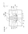
- FIG. 3 is a partially enlarged view of the detection unit 32 of the present embodiment as viewed from above in the device height direction.
- the detection unit 32 includes a plurality of detection elements 60, a wiring board 70, and a plurality of wires 80.
- the wiring board 70 (and the detection unit 32) is long and is arranged along the Y direction (see FIGS. 1 and 2 ).
- the plurality of detection elements 60 are linearly arranged on the wiring board 70 along the longitudinal direction of the wiring board 70, that is, the Y direction, with the detection elements 60 facing the same direction.
- Each detection element 60 of the present embodiment is, for example, an SBD.
- a basic pattern 100 is formed.
- Each basic pattern 100 is composed of a first pattern 110 (an example of a first wiring) and a second pattern 120 (an example of a second wiring).
- the arrangement interval of the basic patterns 100 is, for example, the same as the arrangement interval of the detection elements 60.
- the plurality of basic patterns 100 are arranged at positions offset in the X direction with respect to the plurality of detection elements 60.
- FIG. 4 is a partially enlarged view of an arbitrary one detection element 60 of the present embodiment and the basic pattern 100 connected to the one detection element 60 as seen from the upper side in the device height direction.
- the first pattern 110 and the second pattern 120 of the basic pattern 100 are line-symmetric with respect to a virtual straight line A (one-dot chain line in FIG. 4) passing through the center position of the detection element 60 in the Y direction and extending in the X direction. It is said to be a pattern.
- a portion on one end side of the first pattern 110 (a pad 112 described below) is connected to one electrode 62 of the detection element 60 by a wire 80, and a portion on one end side of the second pattern 120 (a pad 122 described below) is the detection element 60.
- the other electrode 64 is connected by a wire 80. That is, the first pattern 110 and the second pattern 120 are connected to the electrodes 62 and 64 of the detection element 60 by wire bonding, respectively.
- the part on the other end side of the first pattern 110 (the part on the side opposite to the pad 112 side) and the part on the other end side of the second pattern 120 (the part on the side opposite to the pad 122 side) are connected to the power supply unit 34.
- the power supply unit 34 includes, as an example, a power supply that applies a bias voltage for each detection element 60 to detect an electromagnetic wave W having a wavelength ⁇ , and a measurement unit that measures a detection signal detected by each detection element 60. And an amplifier that amplifies the detection signal measured by the measurement unit.
- the first pattern 110 has a pad 112 (an example of a first portion), a wiring portion 114 (an example of a second portion), and a wiring portion 116 (an example of a third portion). doing.
- the pad 112 extends in the X direction (an example of the first direction) and is connected to the one electrode 62 of the detection element 60 by the wire 80.
- the length of the pad 112 is 90% or more and 110% or less of n times ⁇ /4 (n is a positive integer).
- the wiring portion 114 extends in a direction different from the Y direction (an example of the second direction), that is, the X direction, and away from the pad 112 with respect to the virtual straight line A. .. That is, the direction in which the wiring portion 114 extends (Y direction in this embodiment) is in the range of 45° or more and 135° or less with respect to the direction in which the pad 112 extends (X direction in this embodiment). Cross at.
- the wiring portion 114 is connected to the end of the pad 112 on the side opposite to the detection element 60 side in the X direction.
- the width w2 of the wiring portion 114 is narrower than the width w1 of the pad 112, for example.
- the length of the wiring portion 114 is longer than the length of the pad 112, for example. That is, the length of the wiring portion 114 is different from the length of the pad 112.
- the wiring portion 116 extends in a direction different from the X direction (an example of the third direction), that is, the Y direction, and away from the wiring portion 114 with respect to the pad 112.
- the wiring portion 116 is connected to the end of the wiring portion 114 on the opposite side to the side connected to the pad 112. That is, the wiring portion 114 is connected to the pad 112 at one end in the Y direction and is connected to the wiring portion 116 at the other end.
- An end portion (not shown) of the wiring portion 116 opposite to the side connected to the wiring portion 114 is connected to the power supply unit 34.
- the second pattern 120 is a line-symmetrical pattern with respect to the first pattern 110 with respect to the virtual straight line A (dotted line in FIG. 4).
- the second pattern 120 has a pad 122 (an example of a first portion), a wiring portion 124 (an example of a second portion), and a wiring portion 126 (an example of a third portion).
- the pad 122, the wiring portion 124, and the wiring portion 126 are line-symmetrical portions with respect to the pad 112, the wiring portion 114, and the wiring portion 116 of the first pattern 110 with respect to the virtual straight line A, respectively.
- the pad 122 is connected to the other electrode 64 of the detection element 60 by the wire 80, as shown in FIG.
- the second pattern 120 has been briefly described. However, since the second pattern 120 is a pattern symmetrical to the first pattern 110 with respect to the virtual straight line A, other description of the second pattern 120 is made. For the above, refer to the description of the first pattern 110.
- the control unit 50 (see FIGS. 1 and 2) has a function of controlling the electromagnetic wave oscillation device 20, the electromagnetic wave detection device 30, and the carrier device 40 during the analysis operation of the object MO by the electromagnetic wave detection system 10 described later.
- the control unit 50 has a storage device 52, as shown in FIGS. 1 and 2.
- the storage device 52 stores a computer program CP for controlling the electromagnetic wave oscillation device 20, the electromagnetic wave detection device 30, and the carrier device 40. Specific functions of the control unit 50 including the contents of the computer program CP will be described in the description of the analysis operation of the object MO by the electromagnetic wave detection system 10 described later.
- the measurer turns on a switch (not shown) of the electromagnetic wave detection system 10 to bring the electromagnetic wave detection system 10 into a measurable state of the object MO.
- the measurer moves the conveyor belt 42 from a predetermined position (a position sandwiched between the electromagnetic wave oscillation device 20 and the electromagnetic wave detection device 30 on the conveyor belt 42 (hereinafter, referred to as an irradiation line of the electromagnetic wave W)).
- the object MO is arranged at a position on the upstream side in the circulation direction).
- the control unit 50 controls the electromagnetic wave oscillation device 20, the electromagnetic wave detection device 30, and the carrier device 40 according to the computer program CP stored in the storage device 52. Then, the analysis operation of the object MO is started.
- the control unit 50 causes the power supply 24 of the electromagnetic wave oscillation device 20 to apply a bias voltage for causing each oscillation element of the oscillation unit 22 to oscillate the electromagnetic wave W having the wavelength ⁇ .
- each oscillating element emits the electromagnetic wave W of wavelength ⁇ toward the lower side in the Z direction (see FIGS. 1 and 2 ).
- the control unit 50 applies a bias voltage to the power supply of the power supply unit 34 of the electromagnetic wave detection device 30 so that each detection element 60 of the detection unit 32 detects the electromagnetic wave W of the wavelength ⁇ emitted from the electromagnetic wave oscillation device 20.
- each detection element 60 (electromagnetic wave detection device 30) detects the electromagnetic wave W of wavelength ⁇ emitted from the electromagnetic wave oscillation device 20 (see FIGS. 1 and 2).
- the control unit 50 drives the drive source of the transfer device 40 to rotate the transfer belt 42 at a predetermined rotation speed.
- the object MO arranged on the conveyor belt 42 moves from the upstream side to the downstream side in the X direction and passes through the irradiation line of the electromagnetic wave W.
- each detection element 60 of the electromagnetic wave detection device 30 detects the electromagnetic wave W that has passed through the object MO and the conveyor belt 42.
- the detection signal detected by each detection element 60 is measured by the measurement unit of the power supply unit 34 via each basic pattern 100.
- the object MO is a paper envelope (not shown) that contains a plastic plate and a metal plate
- the electromagnetic wave W is reflected by the metal plate in the Z direction and detected immediately below the metal plate.
- the element 60 cannot be reached.
- the control unit 50 uses the detection signals detected by the respective detection elements 60 of the electromagnetic wave detection device 30 (that is, the detection signals measured by the measurement unit of the power supply unit 34 and amplified by the amplifier) to detect the object MO 2 Create three-dimensional image data.
- the created image data is displayed as a two-dimensional image on an external device (for example, a display device (not shown)) connected to the control unit 50, for example.
- the control unit 50 turns off the power supply 24 of the electromagnetic wave oscillation device 20 and the power supply unit 34 of the electromagnetic wave detection device 30 and stops the driving of the drive source of the carrier device 40, the target of the electromagnetic wave detection system 10 of the present embodiment.
- the analysis operation of the object MO ends.
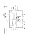
- FIG. 5 is a partially enlarged view of the detection unit 32A included in the electromagnetic wave detection device 30A (electromagnetic wave detection system 10A) of the comparative form as viewed from above.
- the comparative form differs from the present embodiment only in that the basic pattern 100A of the present embodiment (see FIGS. 3 and 4) is replaced with a basic pattern 100A.
- the basic pattern 100A is composed of a first pattern 110A and a second pattern 120A.
- the first pattern 110A has a pad 112A and a wiring portion 114A.
- the pad 112A extends along the Y direction, and its length is not 90% or more and 110% or less of n times ⁇ /4 (n is a positive integer).
- the wiring portion 114A extends from the pad 112A along the X direction and is connected to the power supply unit 34.
- the second pattern 120A is line-symmetrical to the first pattern 110A with respect to the virtual straight line A. That is, the pad 122A and the wiring portion 124A of the second pattern 120A are line-symmetrical portions with respect to the pad 112A and the wiring portion 114A of the first pattern 110A with respect to the virtual straight line A, respectively.
- the above is the description of the configuration of the comparative example.
- the detection signal is measured by the measuring unit of the power supply unit 34 via the basic pattern 100A.
- the electromagnetic wave W having the wavelength ⁇ is detected only by the antenna of each detection element 60. That is, in the comparative mode, only the polarized wave in one direction by the antenna of each detection element 60 can be detected.
- the imaging devices disclosed in Non-Patent Documents 1 and 2 can detect polarized waves in two directions.
- the detector chip for detecting polarized waves in two directions is composed of two SBDs.
- the first pattern 110 of the present embodiment has the pad 112 extending in the X direction and the wiring portion 114 extending from the pad 112 in the Y direction different from the X direction, and the length of the pad 112 is smaller than that of the pad 112. It is set to 90% or more and 110% or less of n times ⁇ /4 (n is a positive integer) (see FIG. 4 and the like).
- the second pattern 120 of the present embodiment has the pad 122 extending in the X direction and the wiring portion 124 extending from the pad 122 in the Y direction different from the X direction, and the length of the pad 122 is ⁇ /4. N times (n is a positive integer) 90% or more and 110% or less.
- the pad 112 of the first pattern 110 is different from the polarized wave detected by each detection element 60 by using the wiring board 70 (specifically, by using a part of the wiring board 70 as a ground plane). It functions as a monopole antenna that detects polarized waves in the direction. That is, the pad 112 of the present embodiment functions as an antenna that detects polarized waves in a direction that cannot be detected by the detection element 60, in addition to a function for electrical connection with the detection element 60.
- the pad 122 of the second pattern 120 also performs the two functions of the pad 112 of the first pattern 110.
- the electromagnetic wave detection device 30 of the present embodiment can detect polarized waves in two directions without adding detection elements. Further, the electromagnetic wave detection device 30 (electromagnetic wave detection system 10) of the present embodiment can detect polarized waves in two directions at low cost (with a simple configuration). In addition, in the case of the present embodiment, since the first pattern 110 and the second pattern 120 each have a configuration that exhibits two functions, only one of the first pattern 110 and the second pattern 120 has two functions. The detection sensitivity of the electromagnetic wave W having the wavelength ⁇ is higher than that in the case of having the configuration to exert the effect.
- the wiring portion 114 of the first pattern 110 extends in a direction different from that of the pad 112, and the width w2 of the wiring portion 114 is narrower than the width w1 of the pad 112. Therefore, it is easy for the pad 112 to function as a monopole antenna that detects the electromagnetic wave W having the wavelength ⁇ .
- This effect is an effect that is also exhibited in the case of the second pattern 120.
- the wiring portion 114 of the first pattern 110 extends 45° or more and 135° or less with respect to the pad 112, specifically, in a direction orthogonal to the pad 112.
- the wiring portion 114 of the first pattern 110 extends in a direction intersecting the pad 112 by 10° or less, a combination of a portion of the wiring portion 114 and the pad 112 serves as an antenna, and the wavelength ⁇
- the electromagnetic wave W may not be detected stably. Therefore, in the case of the present embodiment, the pad 112 easily exhibits the function as a monopole antenna that detects the electromagnetic wave W having the wavelength ⁇ . This effect is an effect that is also exhibited in the case of the second pattern 120.
- the electromagnetic wave detection device 30 of the present embodiment arranges a plurality of combinations for detecting polarized waves in two directions linearly by one detection element 60 and the basic pattern 100, and linearly irradiates the electromagnetic wave W having the wavelength ⁇ . It is detected (see FIGS. 1 to 3).
- the imaging devices disclosed in Non-Patent Documents 1 and 2 also detect polarized waves in two directions by using a plurality of detector chips arranged in a straight line. However, in the imaging device, the number of SBDs (corresponding to the detection element 60 of the present embodiment) is twice as large as that of the present embodiment.
- the electromagnetic wave detection device 30 of the present embodiment detects polarization in two directions by reducing the number of detection elements 60 by half (or about that) as compared with the imaging devices disclosed in Non-Patent Documents 1 and 2. can do. Accordingly, the electromagnetic wave detection device 30 of the present embodiment has a high degree of freedom in the layout of the detection elements 60 on the wiring board 70. Further, in the electromagnetic wave detection device 30 of this embodiment, the detection unit 32 can be downsized.
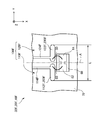
- FIG. 6A is a top view of one detection element 60 included in the detection unit 32B included in the electromagnetic wave detection device 30B (electromagnetic wave detection system 10B) of this modification and the basic pattern 100B connected to the one detection element 60.
- FIG. This modified example is different from the first embodiment only in that a basic pattern 100B is used instead of the basic pattern 100 (see FIG. 4) of the first embodiment.
- the basic pattern 100B is composed of a first pattern 110B and a second pattern 120B.
- the first pattern 110B has a pad 112B (an example of a first portion), a wiring portion 114B (an example of a second portion), and a wiring portion 116B (an example of a third portion).
- the first pattern 110B and the second pattern 120B are line-symmetric with respect to the virtual straight line A.
- the pad 112B extends along the X direction and has a length of 90% or more and 110% or less of n times ⁇ /4 (n is a positive integer).
- the wiring portion 114B extends from the pad 112B along the X direction.
- the wiring portion 116B extends in the X direction from the wiring portion 114B and is connected to the power supply unit 34.
- the pad 112B and the pad 122B of the second pattern 120B are arranged outside the detection element 60 in the Y direction.
- the wiring portions 114B and 124B extend from the pads 112B and 122B so as to approach the virtual straight line A, respectively.
- the pads 112B and 122B are detected by the respective detection elements 60 by using the wiring board 70 (specifically, by using a part of the wiring board 70 as a ground surface). It functions as a monopole antenna that detects polarized waves in a direction different from that of polarized waves.
- the effects of this modification are similar to those of the first embodiment.
- FIG. 6B is a top view of one detection element 60 included in the detection unit 32C included in the electromagnetic wave detection device 30C (electromagnetic wave detection system 10C) of the present modification and the basic pattern 100C connected to the one detection element 60.
- FIG. This modified example is different from the first embodiment only in that a basic pattern 100C is used instead of the basic pattern 100 (see FIG. 4) of the first embodiment.
- the basic pattern 100C is composed of a first pattern 110 and a second pattern 120C.
- the pad 122C of the second pattern 120C extends along the X direction and has a length of 90% or more and 110% or less of n times ⁇ /4 (n is a positive integer).
- the difference from the case of the first embodiment is that the length is not more than the length.
- the length of the pad 122C is shorter than the length of the pad 112. That is, in this modification, the first pattern 110 and the second pattern 120C are not line-symmetric with respect to the virtual straight line A.
- the pad 122C cannot function as a monopole antenna, but the pad 112 can function as a monopole antenna.
- the effects of this modification are similar to those of the first embodiment.
- FIG. 6C is a top view of one detection element 60 included in the detection unit 32D included in the electromagnetic wave detection device 30D (electromagnetic wave detection system 10D) of this modification and the basic pattern 100D connected to the one detection element 60.
- FIG. This modification is different from the first embodiment only in that the basic pattern 100D (see FIG. 4) of the first embodiment is replaced with a basic pattern 100D.
- the basic pattern 100D is composed of a first pattern 110D and a second pattern 120D.
- the wiring portion 114D of the first pattern 110D of the present modification extends in a direction inclined with respect to the Y direction (and the X direction), and the wiring portion 124D of the second pattern 120D includes the Y direction (and the X direction).
- the direction in which the wiring portion 124D extends is 45° with respect to the direction in which the pad 122 extends (the X direction in the present embodiment). It intersects in the range of not less than 135°.
- the first pattern 110D and the second pattern 120D are line-symmetrical with respect to the virtual straight line A.
- the pads 112 and 122 can be made to function as a monopole antenna.
- the effects of this modification are similar to those of the first embodiment.
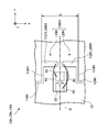
- FIG. 7 shows one detection element 60 included in the detection unit 32E included in the electromagnetic wave detection device 30E (electromagnetic wave detection system 10E) of the present embodiment, and the basic pattern 100E connected to the one detection element 60 in the device height. It is the elements on larger scale seen from the upper side of a direction.
- the present embodiment differs from the first embodiment only in that a basic pattern 100E is used instead of the basic pattern 100 (see FIG. 4) of the first embodiment.
- the basic pattern 100E is composed of a first pattern 110E and a second pattern 120E.
- the first pattern 110E has a pad 112E (an example of a first portion), a wiring portion 114E (an example of a second portion), and a wiring portion 116E (an example of a third portion).
- the pad 112E is arranged on one side in the Y direction with respect to the detection element 60, and extends in the X direction (an example of the first direction).
- the wiring portion 114E is connected to the end portion of the pad 112E and extends from one side in the Y direction (an example of the second direction) to the other side.
- the wiring portion 116E is connected to the end of the wiring portion 114E on the side opposite to the side to which the pad 112E is connected, extends in the X direction, and is connected to the power supply unit 34.
- the second pattern 120E and the first pattern 110E are point-symmetric with respect to the center O of the detection element 60.
- the pad 122E (an example of the first portion), the wiring portion 124E (an example of the second portion) and the wiring portion 126E (an example of the third portion) of the second pattern 120E are the pad 112E of the first pattern 110E, respectively.
- the wiring portion 114E and the wiring portion 116E are point-symmetrical portions. An end of the wiring portion 126E opposite to the side connected to the wiring portion 124E is connected to the power supply unit 34.
- the pad 112E of the first pattern 110E and the pad 122E of the second pattern 120E are arranged at least offset in the X direction to form a pair (hereinafter referred to as a connected It is called part 200).
- the length L from the one end to the other end of the connected portion 200 in the X direction is 90% or more and 110% or less of n times ⁇ /2 (n is a positive integer).
- the combination of the pad 112E and the pad 122E, that is, the connected portion 200 can be made to function as a dipole antenna that detects a polarization in a direction different from the polarization detected by each detection element 60.
- the effects of this modification are similar to those of the first embodiment.
- FIG. 8A is a top view of one detection element 60 included in the detection unit 32F included in the electromagnetic wave detection device 30F (electromagnetic wave detection system 10F) of this modification and the basic pattern 100F connected to the one detection element 60.
- FIG. This modified example is different from the second embodiment only in that the basic pattern 100E (see FIG. 7) of the second embodiment is replaced with a basic pattern 100F.
- the basic pattern 100F is composed of a first pattern 110F and a second pattern 120F.
- the first pattern 110F has a pad 112F (an example of a first portion) and a wiring portion 114F (an example of a second portion).
- the pad 112F extends along the Y direction (an example of the first direction) and has a length of 90% or more and 110% or less of n times ⁇ /4 (n is a positive integer).
- the wiring portion 114F extends from the pad 112F in the X direction (an example of the second direction) and is connected to the power supply unit 34.
- the second pattern 120F and the first pattern 110F are line-symmetric with respect to the virtual straight line A.
- the pad 122F (an example of the first portion) and the wiring portion 124F (an example of the second portion) of the second pattern 120F are connected to the pad 112F and the wiring portion 114F of the first pattern 110F and the virtual straight line A, respectively. It is considered to be a line-symmetrical part.
- the end of the wiring portion 124F on the side opposite to the side connected to the pad 122F is connected to the power supply unit 34.
- the pad 112F included in the first pattern 110F and the pad 122F included in the second pattern 120F are arranged at least displaced in the Y direction to form a pair (hereinafter, referred to as a connection target). Part 200F).
- the length L from the one end to the other end of the connected portion 200F in the Y direction is 90% or more and 110% or less of n times ⁇ /2 (n is a positive integer).
- the combination of the pad 112F and the pad 122F, that is, the connected portion 200F can be made to function as a dipole antenna that detects a polarization in a direction different from the polarization detected by each detection element 60.
- the effects of this modification are similar to those of the second embodiment.
- FIG. 8B is a top view of one detection element 60 included in the detection unit 32G included in the electromagnetic wave detection device 30G (electromagnetic wave detection system 10G) of the present modification and the basic pattern 100G connected to the one detection element 60.
- FIG. This modification is different from the second embodiment only in that the basic pattern 100E (see FIG. 7) of the second embodiment is replaced with a basic pattern 100G.
- the basic pattern 100G is composed of a first pattern 110G and a second pattern 120G.
- the first pattern 110G has a pad 112G (an example of a first portion) and a wiring portion 114G (an example of a second portion).
- the pad 112G extends along the Y direction (an example of the first direction) and has a length of 90% or more and 110% or less of n times ⁇ /4 (n is a positive integer).
- the wiring portion 114G extends from the pad 112G along the X direction (an example of the second direction) and is connected to the power supply unit 34.
- the second pattern 120G and the first pattern 110G are point-symmetric with respect to the center O of the detection element 60.
- the pad 122G (an example of the first portion) and the wiring portion 124G (an example of the second portion) of the second pattern 120G are pointed with respect to the pad 112G and the wiring portion 114G of the first pattern 110G and the center O, respectively. It is considered to be a symmetrical part.
- An end of the wiring portion 124G on the side opposite to the side connected to the pad 122G is connected to the power supply unit 34.
- the pad 112G included in the first pattern 110G and the pad 122G included in the second pattern 120G are arranged so as to be displaced at least in the Y direction to form a pair (hereinafter, to be connected).
- the length L from the one end to the other end of the connected portion 200G in the Y direction is 90% or more and 110% or less of n times ⁇ /2 (n is a positive integer).
- the combination of the pad 112G and the pad 122G, that is, the connected portion 200G can be made to function as a dipole antenna that detects a polarization in a direction different from the polarization detected by each detection element 60.
- the effects of this modification are similar to those of the second embodiment.
- FIG. 8C is a top view of one detection element 60 included in the detection unit 32H included in the electromagnetic wave detection device 30H (electromagnetic wave detection system 10H) of the present modification and the basic pattern 100H connected to the one detection element 60.
- FIG. This modification is different from the second embodiment only in that a basic pattern 100H (see FIG. 7) of the second embodiment is replaced with a basic pattern 100H.
- the basic pattern 100H is composed of a first pattern 110H and a second pattern 120H.
- the first pattern 110H has a pad 112H (an example of a first portion), a wiring portion 114H (an example of a second portion), and a wiring portion 116H (an example of a third portion).
- the pad 112H extends along the X direction (an example of the first direction) and has a length of 90% or more and 110% or less of n times ⁇ /4 (n is a positive integer).
- the wiring portion 114H extends from the pad 112H along the Y direction (an example of the second direction).
- the wiring portion 116H extends in the X direction from the end of the wiring portion 114H on the side opposite to the side to which the pad 112H is connected, and is further connected to the power supply unit 34.
- the second pattern 120H is line-symmetrical to the first pattern 110H with respect to the virtual straight line B (one-dot chain line in FIG. 8C) passing through the center position of the detection element 60 in the X direction and extending in the Y direction. It is said that.
- the pad 122H (an example of a first portion), the wiring portion 124H (an example of a second portion) and the wiring portion 126H (an example of a third portion) of the second pattern 120H are respectively the pad 112H of the first pattern 110H,
- the wiring portion 114H and the wiring portion 116H are symmetrical with respect to the virtual straight line B.
- An end of the wiring portion 124H on the side opposite to the side connected to the pad 122H is connected to the power supply unit 34.
- the pad 112H included in the first pattern 110H and the pad 122H included in the second pattern 120H are arranged at least offset in the X direction to form a pair (hereinafter, referred to as a connection target). Part 200H).
- the length L from the one end to the other end of the connected portion 200H in the Y direction is 90% or more and 110% or less of n times ⁇ /2 (n is a positive integer).
- the combination of the pad 112H and the pad 122H, that is, the connected portion 200H can be made to function as a dipole antenna that detects a polarization in a direction different from the polarization detected by each detection element 60.
- the effects of this modification are similar to those of the second embodiment.
- FIG. 8D is a top view of one detection element 60 included in the detection unit 32I included in the electromagnetic wave detection device 30I (electromagnetic wave detection system 10I) of the present modification and the basic pattern 100I connected to the one detection element 60 from above.
- FIG. This modification is different from the second embodiment only in that a basic pattern 100E (see FIG. 7) of the second embodiment is replaced with a basic pattern 100I.
- the basic pattern 100I is composed of a first pattern 110I and a second pattern 120I.
- the wiring portion 114I (an example of the second portion) of the first pattern 110I of the present modification extends in the direction inclined with respect to the Y direction (and the X direction)
- the wiring portion 124I of the second pattern 120I An example of the second portion extends in a direction inclined with respect to the Y direction (and the X direction).
- the first pattern 110I and the second pattern 120I are point-symmetric with respect to the center O of the detection element 60.
- the pad 112E of the first pattern 110I and the pad 122E of the second pattern 120I are arranged at least offset in the X direction to form a pair (the connected portion 200). ).
- the length L from the one end to the other end of the connected portion 200 in the Y direction is 90% or more and 110% or less of n times ⁇ /2 (n is a positive integer).
- the combination of the pad 112E and the pad 122E, that is, the connected portion 200 can be made to function as a dipole antenna that detects a polarization in a direction different from the polarization detected by each detection element 60.
- the effects of this modification are similar to those of the second embodiment.
- the present invention has been described by taking the first embodiment and its modifications (first to third modifications) and the second embodiment and its modifications (fourth to seventh modifications) as examples.
- the invention is not limited to these forms.
- the technical scope of the present invention further includes the following forms (modifications).
- the detection unit 32 and the like have been described as having a plurality of detection elements 60 (see FIG. 3 ).
- the number of detection elements 60 may be one.
- each embodiment and each modified example which are examples of the present invention have been described separately.
- a configuration in which one of the embodiments and each modification is combined with the components of each of the other embodiments and each modification also belongs to the technical scope of the present invention.
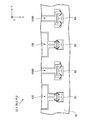
- a combination of one detection element 60 and the basic pattern 100 such as the detection unit 32J included in the electromagnetic wave detection device 30J (electromagnetic wave detection system 10J) of the eighth modification shown in FIG.
- a combination of one detection element 60 and the basic pattern 100B may be linearly arranged.
- the plurality of detection elements 60 of each embodiment and each modification are linearly arranged in the Y direction (see FIG. 3 ).
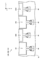
- the interpretation is "straight line", but it is not necessary to connect a plurality of detection elements 60 to form a straight line. That is, “straightly” means, for example, each detection element 60 along the Y direction, like the detection unit 32K included in the electromagnetic wave detection device 30K (electromagnetic wave detection system 10K) of the ninth modification shown in FIG. Are arranged in a staggered pattern, but it means that they may be linear as a whole.
- each basic pattern 100 of the first embodiment is arranged on the same side in the X direction with respect to each detection element 60 as an example (see FIG. 3).
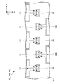
- the basic patterns 100 may be arranged in a staggered manner, for example, like the detection unit 32L included in the electromagnetic wave detection device 30L (electromagnetic wave detection system 10L) of the tenth modification shown in FIG.
- the arrangement interval of the plurality of detection elements 60 arranged along the Y direction can be made narrower than in the case of the present embodiment (see FIG. 3 ), for example.
- the electromagnetic wave detection system 10 of the present exemplary embodiment includes the electromagnetic wave oscillation device 20, the electromagnetic wave detection device 30, and the carrier device 40.
- the detection operation is performed. (See FIGS. 1 and 2).
- the carrier device 40 may be omitted.
- the configuration in which the electromagnetic wave oscillation device 20 and the electromagnetic wave detection device 30 are integrated may move with respect to the object MO.
- the movement of the object MO by the carrier device 40 may be the movement of the configuration in which the electromagnetic wave oscillation device 20 and the electromagnetic wave detection device 30 are integrated. Good.
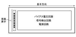
- the electromagnetic wave oscillating device 20 of the present embodiment has been described as being long and arranged with its longitudinal direction along the Y direction (see FIGS. 1 and 2). However, as in the case of the twelfth modified example of FIG. 13, the longitudinal direction thereof may be arranged along the X direction.
- the electromagnetic wave oscillation device belonging to the technical scope of the present invention may be a combination of a terahertz wave generation unit and a cylindrical lens as in the case of the thirteenth modified example of FIG.
- the combination is a unit that generates a terahertz wave of about 100 GHz, for example.
- the irradiation range of the electromagnetic wave in the Y direction can be expanded by the cylindrical lens.
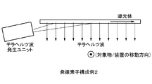
- the electromagnetic wave oscillation device within the technical scope of the present invention may be a combination of a terahertz wave generation unit and a light guide, as in the case of the fourteenth modified example of FIG.
- the terahertz wave emitted from the terahertz wave generating unit may be obliquely incident on the light guide.
- the electromagnetic wave detection device 30, 30B to 30L is described as one component of the electromagnetic wave detection system 10, 10B to 10L (see FIGS. 1 and 2).
- the electromagnetic wave detection device 30 and the like may be used as a single device instead of one component of the electromagnetic wave detection system 10 and the like.
- it may be used as a signal detection system device (reception device) or other device for automatic driving of an automobile.
Landscapes
- Physics & Mathematics (AREA)
- Spectroscopy & Molecular Physics (AREA)
- General Physics & Mathematics (AREA)
- Health & Medical Sciences (AREA)
- Chemical & Material Sciences (AREA)
- Life Sciences & Earth Sciences (AREA)
- Toxicology (AREA)
- Analytical Chemistry (AREA)
- Biochemistry (AREA)
- General Health & Medical Sciences (AREA)
- Immunology (AREA)
- Pathology (AREA)
- Investigating Or Analysing Materials By Optical Means (AREA)
Abstract
本発明の電磁波検出装置は、波長λの電磁波を検出する少なくとも1つの検出素子と、前記少なくとも1つの検出素子の一方の電極に接続されている第1配線と、前記少なくとも1つの検出素子の他方の電極に接続されている第2配線と、を備え、前記第1配線及び前記第2配線の少なくとも一方は、前記一方の電極又は前記他方の電極に接続され、第1方向に延在する第1部分及び前記第1部分から前記第1方向と異なる第2方向に延在する第2部分を有し、前記第1部分の長さは、λ/4のn倍(nは正の整数)の90%以上110%以下とされている。
Description
本発明は、電磁波検出装置及び電磁波検出システムに関する。
非特許文献1には、ベルトコンベアで搬送される食品にビーム幅約90mmのテラヘルツ波を照射し、食品を透過したテラヘルツ波を検出器で検出することで2次元画像を得るイメージング装置が開示されている。この検出器は、垂直偏波及び水平偏波を独立に検出するためにショットキーバリアダイオード(以下、SBDという。)を2個用いた検出器チップを、一次元に合計50個、2mmピッチで配列した構成とされている。
また、非特許文献2は、非特許文献1の一部の著者により発表され、食品を透過したテラヘルツ波を検出器で検出することで2次元画像を得るイメージング装置が開示された文献である。非特許文献2の検出器チップを構成する2個のSBDは、互いに直交する向きに向いた状態で配置されている。
また、非特許文献2は、非特許文献1の一部の著者により発表され、食品を透過したテラヘルツ波を検出器で検出することで2次元画像を得るイメージング装置が開示された文献である。非特許文献2の検出器チップを構成する2個のSBDは、互いに直交する向きに向いた状態で配置されている。
兪 熊斌、外3名、偏波独立型0.3THz高速テラヘルツイメージング、[online]、平成28年3月22日、応用物理学会春季学術講演会、[平成30年9月13日検索]、インターネット<URL:https://confit.atlas.jp/guide/event-img/jsap2016s/22a-H135-3/public/pdf?type=in>
ベイ ジョンソク、外2名、THzテラヘルツイメージング ~テラヘルツ波の高い透過性を利用~、[online]、[平成30年11月1日検索]、インターネット<URL:http://www.chinokyoten.pref.aichi.jp/project01-03/pdf/18.pdf>
上記の検出器チップは、垂直偏波及び水平偏波(2方向の偏波)を検出するために、2個のSBD(検出素子)を用いている。別の見方をすると、上記の検出器チップは、1個の検出素子では検出できない2方向の偏波のうちの1方向の偏波を、増設したもう1個の検出素子に検出させている。
本発明が解決しようとする課題としては、検出素子を増設することなく2方向の偏波の検出を可能にすることが一例として挙げられる。
請求項1に記載の発明は、
波長λの電磁波を検出する少なくとも1つの検出素子と、
前記少なくとも1つの検出素子の一方の電極に接続されている第1配線と、
前記少なくとも1つの検出素子の他方の電極に接続されている第2配線と、
を備え、
前記第1配線及び前記第2配線の少なくとも一方は、前記一方の電極又は前記他方の電極に接続され、第1方向に延在する第1部分及び前記第1部分から前記第1方向と異なる第2方向に延在する第2部分を有し、
前記第1部分の長さは、λ/4のn倍(nは正の整数)の90%以上110%以下とされている、
電磁波検出装置である。
波長λの電磁波を検出する少なくとも1つの検出素子と、
前記少なくとも1つの検出素子の一方の電極に接続されている第1配線と、
前記少なくとも1つの検出素子の他方の電極に接続されている第2配線と、
を備え、
前記第1配線及び前記第2配線の少なくとも一方は、前記一方の電極又は前記他方の電極に接続され、第1方向に延在する第1部分及び前記第1部分から前記第1方向と異なる第2方向に延在する第2部分を有し、
前記第1部分の長さは、λ/4のn倍(nは正の整数)の90%以上110%以下とされている、
電磁波検出装置である。
上述した目的、およびその他の目的、特徴および利点は、以下に述べる好適な実施の形態、およびそれに付随する以下の図面によってさらに明らかになる。
≪概要≫
以下、本発明の一例である第1実施形態及びその変形例(第1~第3変形例)並びに第2実施形態及びその変形例(第4~第7変形例)について図面を参照しながら説明する。次いで、その他の変形例(第8~第14変形例)について図面を参照しながら説明する。なお、参照するすべての図面では同様の機能を有する構成要素に同様の符号を付し、明細書では適宜説明を省略する。
以下、本発明の一例である第1実施形態及びその変形例(第1~第3変形例)並びに第2実施形態及びその変形例(第4~第7変形例)について図面を参照しながら説明する。次いで、その他の変形例(第8~第14変形例)について図面を参照しながら説明する。なお、参照するすべての図面では同様の機能を有する構成要素に同様の符号を付し、明細書では適宜説明を省略する。
≪第1実施形態≫
以下、第1実施形態について図面を参照しながら説明する。まず、本実施形態の電磁波検出システム10(図1及び図2参照)の機能及び構成について説明する。次いで、本実施形態の電磁波検出システム10による対象物MO(図1及び図2参照)の解析動作について説明する。次いで、本実施形態の効果について説明する。
以下、第1実施形態について図面を参照しながら説明する。まず、本実施形態の電磁波検出システム10(図1及び図2参照)の機能及び構成について説明する。次いで、本実施形態の電磁波検出システム10による対象物MO(図1及び図2参照)の解析動作について説明する。次いで、本実施形態の効果について説明する。
<第1実施形態の電磁波検出システムの機能及び構成>
図1は、本実施形態の電磁波検出システム10を用いて対象物MOの検査動作を行っている状態を示す図であって、側面側から見た概略図である。また、図2は、本実施形態の電磁波検出システム10を用いて対象物MOの検査動作を行っている状態を示す図であって、正面側から見た概略図である。図1及び図2における符号X、Y、Zは、それぞれ、後述する電磁波検出装置30が備える検出部32の短手方向及び対象物MOの搬送方向、検出部32の長手方向、電磁波Wの照射方向及び電磁波検出システム10の高さ方向(以下、装置高さ方向という。)を意味する。なお、符号X、Y、Zの方向の意味は、図1及び図2以外の図面の場合も同じとする。
図1は、本実施形態の電磁波検出システム10を用いて対象物MOの検査動作を行っている状態を示す図であって、側面側から見た概略図である。また、図2は、本実施形態の電磁波検出システム10を用いて対象物MOの検査動作を行っている状態を示す図であって、正面側から見た概略図である。図1及び図2における符号X、Y、Zは、それぞれ、後述する電磁波検出装置30が備える検出部32の短手方向及び対象物MOの搬送方向、検出部32の長手方向、電磁波Wの照射方向及び電磁波検出システム10の高さ方向(以下、装置高さ方向という。)を意味する。なお、符号X、Y、Zの方向の意味は、図1及び図2以外の図面の場合も同じとする。
本実施形態の電磁波検出システム10は、一例として、対象物MOに電磁波Wを照射し、対象物MOが透過した電磁波Wを検出して、対象物MOの形状等を測定する機能を有する。本実施形態の電磁波検出システム10は、図1及び図2に示されるように、電磁波発振装置20と、電磁波検出装置30と、搬送装置40と、制御部50とを備えている。
〔電磁波発振装置及び搬送装置〕
本実施形態の電磁波発振装置20は、図1及び図2に示されるように、Z方向の下側に向けて波長λの電磁波Wを照射する機能を有する。電磁波発振装置20は、長尺とされ、その長手方向をY方向に沿わせた状態で配置されている。電磁波発振装置20は、発振部22と、電源24とを有している。発振部22は、長尺とされ、Y方向に沿って配置されている。発振部22には、その長手方向に沿って並べられ、それぞれ波長λの電磁波Wを発振する複数の発振素子(図示省略)が実装されている。ここで、本明細書では、各発振素子が発振する波長λの電磁波Wとは、各発振素子が発振する電磁波Wの中心波長が波長λである電磁波Wを意味する。電源24は、各発振素子が電磁波Wを発振するためのバイアス電圧を各発振素子に印加するようになっている。なお、詳細な説明は省略するが、各発振素子は、それぞれ2本の配線(図示省略)により電源24に接続されている。
本実施形態の電磁波発振装置20は、図1及び図2に示されるように、Z方向の下側に向けて波長λの電磁波Wを照射する機能を有する。電磁波発振装置20は、長尺とされ、その長手方向をY方向に沿わせた状態で配置されている。電磁波発振装置20は、発振部22と、電源24とを有している。発振部22は、長尺とされ、Y方向に沿って配置されている。発振部22には、その長手方向に沿って並べられ、それぞれ波長λの電磁波Wを発振する複数の発振素子(図示省略)が実装されている。ここで、本明細書では、各発振素子が発振する波長λの電磁波Wとは、各発振素子が発振する電磁波Wの中心波長が波長λである電磁波Wを意味する。電源24は、各発振素子が電磁波Wを発振するためのバイアス電圧を各発振素子に印加するようになっている。なお、詳細な説明は省略するが、各発振素子は、それぞれ2本の配線(図示省略)により電源24に接続されている。
各発振素子は、一例として、共鳴トンネルダイオード(以下、RTDという。)とされており、電磁波Wの一例としてテラヘルツ波を発振するようになっている。
ここで、テラヘルツ波とは、ミリ波よりも短波長で赤外線よりも長波長の電磁波と言われている。テラヘルツ波は、光波及び電波の両方の性質を兼ね備えていた電磁波であり、例えば、布、紙、木、プラスチック、陶磁器等を透過し(又は透過し易く)、金属、水等は透過しない(又は透過し難い)という性質を有する。一般的に、テラヘルツ波の周波数は1THz前後(波長は300μm前後に相当)の電磁波とも言われているが、その範囲について一般的に明確な定義はない。そこで、本明細書では、テラヘルツ波の周波数の範囲を80GHz以上10THz以下の範囲と定義する。なお、前述の説明では、各発振素子はRTDとされているとしたが、テラヘルツ波を発振させる素子であれば各発振素子はRTDでなくてもよい。
ここで、テラヘルツ波とは、ミリ波よりも短波長で赤外線よりも長波長の電磁波と言われている。テラヘルツ波は、光波及び電波の両方の性質を兼ね備えていた電磁波であり、例えば、布、紙、木、プラスチック、陶磁器等を透過し(又は透過し易く)、金属、水等は透過しない(又は透過し難い)という性質を有する。一般的に、テラヘルツ波の周波数は1THz前後(波長は300μm前後に相当)の電磁波とも言われているが、その範囲について一般的に明確な定義はない。そこで、本明細書では、テラヘルツ波の周波数の範囲を80GHz以上10THz以下の範囲と定義する。なお、前述の説明では、各発振素子はRTDとされているとしたが、テラヘルツ波を発振させる素子であれば各発振素子はRTDでなくてもよい。
本実施形態の搬送装置40は、無端状の搬送ベルト42と、駆動源(図示所略)とを有している。駆動源は、搬送ベルト42を定められた周回速度で周回させる機能を有する。
搬送ベルト42は、Z方向において、電磁波発振装置20の下側かつ電磁波検出装置30の上側に配置され、駆動源に駆動されて、配置された対象物MOをX方向(図1の矢印の方向)に搬送するようになっている。なお、本実施形態の搬送ベルト42は、テラヘルツ波を透過可能な材料(例えば、プラスチック)で形成されている。
搬送ベルト42は、Z方向において、電磁波発振装置20の下側かつ電磁波検出装置30の上側に配置され、駆動源に駆動されて、配置された対象物MOをX方向(図1の矢印の方向)に搬送するようになっている。なお、本実施形態の搬送ベルト42は、テラヘルツ波を透過可能な材料(例えば、プラスチック)で形成されている。
〔電磁波検出装置〕
本実施形態の電磁波検出装置30は、図1及び図2に示されるように、電磁波発振装置20の各発振素子が発振して照射した波長λの電磁波Wを検出する機能を有する。電磁波検出装置30を構成する複数の検出素子は、その並び方向をY方向に沿わせた状態で配置されている。電磁波検出装置30は、検出部32と、電源ユニット34とを有している。
本実施形態の電磁波検出装置30は、図1及び図2に示されるように、電磁波発振装置20の各発振素子が発振して照射した波長λの電磁波Wを検出する機能を有する。電磁波検出装置30を構成する複数の検出素子は、その並び方向をY方向に沿わせた状態で配置されている。電磁波検出装置30は、検出部32と、電源ユニット34とを有している。
ここで、図3は、本実施形態の検出部32を装置高さ方向の上側から見た部分拡大図である。検出部32は、複数の検出素子60と、配線基板70と、複数のワイヤ80とを有している。配線基板70(及び検出部32)は、長尺とされ、Y方向に沿わせて配置されている(図1及び図2参照)。
〈複数の検出素子〉
複数の検出素子60は、図3に示されるように、それぞれ同じ向きを向いた状態で、配線基板70の長手方向、すなわち、Y方向に沿って配線基板70に直線状に並べられている。本実施形態の各検出素子60は、一例として、SBDとされている。
複数の検出素子60は、図3に示されるように、それぞれ同じ向きを向いた状態で、配線基板70の長手方向、すなわち、Y方向に沿って配線基板70に直線状に並べられている。本実施形態の各検出素子60は、一例として、SBDとされている。
〈複数の基本パターン〉
また、図3に示されるように、配線基板70の上面(装置高さ方向の上側の面)には、Y方向に沿って並べられている複数(複数の検出素子60と同じ個数の)の基本パターン100が形成されている。各基本パターン100は、第1パターン110(第1配線の一例)と、第2パターン120(第2配線の一例)とで構成されている。各基本パターン100の配置間隔は、一例として、各検出素子60の配置間隔と同じ配置間隔とされている。なお、本実施形態の検出部32では、複数の基本パターン100は、複数の検出素子60に対してX方向にオフセットした位置に配置されている。
また、図3に示されるように、配線基板70の上面(装置高さ方向の上側の面)には、Y方向に沿って並べられている複数(複数の検出素子60と同じ個数の)の基本パターン100が形成されている。各基本パターン100は、第1パターン110(第1配線の一例)と、第2パターン120(第2配線の一例)とで構成されている。各基本パターン100の配置間隔は、一例として、各検出素子60の配置間隔と同じ配置間隔とされている。なお、本実施形態の検出部32では、複数の基本パターン100は、複数の検出素子60に対してX方向にオフセットした位置に配置されている。
図4は、本実施形態の任意の1個の検出素子60及び1個の検出素子60に接続されている基本パターン100を装置高さ方向の上側から見た部分拡大図である。基本パターン100の第1パターン110と第2パターン120とは、一例として、検出素子60のY方向の中心位置を通りX方向に沿った仮想直線A(図4における一点鎖線)に対して線対称のパターンとされている。第1パターン110の一端側の部分(後述するパッド112)は検出素子60の一方の電極62にワイヤ80により接続され、第2パターン120の一端側の部分(後述するパッド122)は検出素子60の他方の電極64にワイヤ80により接続されている。すなわち、第1パターン110及び第2パターン120は、それぞれ、検出素子60の電極62、64にワイヤボンディングにより接続されている。なお、第1パターン110の他端側の部分(パッド112側と反対側の部分)及び第2パターン120の他端側の部分(パッド122側と反対側の部分)は、電源ユニット34に接続されている。電源ユニット34は、一例として、各検出素子60が波長λの電磁波Wを検出するためのバイアス電圧を各検出素子60に印加する電源と、各検出素子60が検出した検出信号を測定する測定部と、測定部が測定した検出信号を増幅するアンプとを有している。
(第1パターン)
第1パターン110は、図4に示されるように、パッド112(第1部分の一例)と、配線部分114(第2部分の一例)と、配線部分116(第3部分の一例)とを有している。
パッド112は、X方向(第1方向の一例)に延在し、検出素子60の一方の電極62にワイヤ80により接続されている。ここで、パッド112の長さ(X方向における長さ)は、λ/4のn倍(nは正の整数)の90%以上110%以下とされている。
配線部分114は、一例として、Y方向(第2方向の一例)、すなわち、X方向と異なる方向であって、パッド112から前述の仮想直線Aに対して離れる方向に向けて延在している。すなわち、配線部分114が延在する方向(本実施形態の場合はY方向)は、パッド112が延在する方向(本実施形態の場合はX方向)に対して45°以上135°以下の範囲で交差している。配線部分114は、パッド112におけるX方向の検出素子60側と反対側の端部に繋がっている。なお、配線部分114の幅w2は、一例として、パッド112の幅w1よりも狭い。また、配線部分114の長さは、一例として、パッド112の長さよりも長い。すなわち、配線部分114の長さは、パッド112の長さと異なる長さとされている。
配線部分116は、一例として、X方向(第3方向の一例)、すなわち、Y方向と異なる方向であって、配線部分114からパッド112に対して離れる方向に向けて延在している。配線部分116は、配線部分114におけるパッド112と繋がっている側と反対側の端部に繋がっている。すなわち、配線部分114は、Y方向における一端側の端部でパッド112に繋がり、他端側の端部で配線部分116に繋がっている。配線部分116における配線部分114に繋がっている側と反対側の端部(図示省略)は、電源ユニット34に接続されている。
第1パターン110は、図4に示されるように、パッド112(第1部分の一例)と、配線部分114(第2部分の一例)と、配線部分116(第3部分の一例)とを有している。
パッド112は、X方向(第1方向の一例)に延在し、検出素子60の一方の電極62にワイヤ80により接続されている。ここで、パッド112の長さ(X方向における長さ)は、λ/4のn倍(nは正の整数)の90%以上110%以下とされている。
配線部分114は、一例として、Y方向(第2方向の一例)、すなわち、X方向と異なる方向であって、パッド112から前述の仮想直線Aに対して離れる方向に向けて延在している。すなわち、配線部分114が延在する方向(本実施形態の場合はY方向)は、パッド112が延在する方向(本実施形態の場合はX方向)に対して45°以上135°以下の範囲で交差している。配線部分114は、パッド112におけるX方向の検出素子60側と反対側の端部に繋がっている。なお、配線部分114の幅w2は、一例として、パッド112の幅w1よりも狭い。また、配線部分114の長さは、一例として、パッド112の長さよりも長い。すなわち、配線部分114の長さは、パッド112の長さと異なる長さとされている。
配線部分116は、一例として、X方向(第3方向の一例)、すなわち、Y方向と異なる方向であって、配線部分114からパッド112に対して離れる方向に向けて延在している。配線部分116は、配線部分114におけるパッド112と繋がっている側と反対側の端部に繋がっている。すなわち、配線部分114は、Y方向における一端側の端部でパッド112に繋がり、他端側の端部で配線部分116に繋がっている。配線部分116における配線部分114に繋がっている側と反対側の端部(図示省略)は、電源ユニット34に接続されている。
(第2パターン)
前述のとおり、第2パターン120は、第1パターン110と、仮想直線A(図4における一点鎖線)に対して線対称のパターンとされている。第2パターン120は、図4に示されるように、パッド122(第1部分の一例)と、配線部分124(第2部分の一例)と、配線部分126(第3部分の一例)とを有している。
パッド122、配線部分124及び配線部分126は、それぞれ、第1パターン110のパッド112、配線部分114及び配線部分116と、仮想直線Aに対して線対称の部分とされている。
パッド122は、図4に示されるように、検出素子60の他方の電極64にワイヤ80により接続されている。また、配線部分126における配線部分124に繋がっている側と反対側の端部(図示省略)は、電源ユニット34に接続されている。
以上のとおり、第2パターン120について簡単に説明したが、第2パターン120は第1パターン110と仮想直線Aに対して線対称のパターンとされていることから、第2パターン120のその他の説明については第1パターン110の説明を援用されたい。
前述のとおり、第2パターン120は、第1パターン110と、仮想直線A(図4における一点鎖線)に対して線対称のパターンとされている。第2パターン120は、図4に示されるように、パッド122(第1部分の一例)と、配線部分124(第2部分の一例)と、配線部分126(第3部分の一例)とを有している。
パッド122、配線部分124及び配線部分126は、それぞれ、第1パターン110のパッド112、配線部分114及び配線部分116と、仮想直線Aに対して線対称の部分とされている。
パッド122は、図4に示されるように、検出素子60の他方の電極64にワイヤ80により接続されている。また、配線部分126における配線部分124に繋がっている側と反対側の端部(図示省略)は、電源ユニット34に接続されている。
以上のとおり、第2パターン120について簡単に説明したが、第2パターン120は第1パターン110と仮想直線Aに対して線対称のパターンとされていることから、第2パターン120のその他の説明については第1パターン110の説明を援用されたい。
〔制御部〕
制御部50(図1及び図2参照)は、後述する電磁波検出システム10による対象物MOの解析動作の際に、電磁波発振装置20、電磁波検出装置30及び搬送装置40を制御する機能を有する。制御部50は、図1及び図2に示されるように、記憶装置52を有している。記憶装置52には、電磁波発振装置20、電磁波検出装置30及び搬送装置40を制御するためのコンピュータ・プログラムCPが記憶されている。
コンピュータ・プログラムCPの内容を含む制御部50の具体的な機能については、後述する電磁波検出システム10による対象物MOの解析動作の説明の中で説明する。
制御部50(図1及び図2参照)は、後述する電磁波検出システム10による対象物MOの解析動作の際に、電磁波発振装置20、電磁波検出装置30及び搬送装置40を制御する機能を有する。制御部50は、図1及び図2に示されるように、記憶装置52を有している。記憶装置52には、電磁波発振装置20、電磁波検出装置30及び搬送装置40を制御するためのコンピュータ・プログラムCPが記憶されている。
コンピュータ・プログラムCPの内容を含む制御部50の具体的な機能については、後述する電磁波検出システム10による対象物MOの解析動作の説明の中で説明する。
以上が、本実施形態の電磁波検出システムの機能及び構成についての説明である。
<第1実施形態の電磁波検出システムによる対象物の解析動作>
次に、本実施形態の電磁波検出システム10による対象物MOの解析動作について図1~図3を参照しながら説明する。
まず、測定者は、電磁波検出システム10のスイッチ(図示省略)をオンにして、電磁波検出システム10を対象物MOの測定可能な状態にする。
次いで、測定者は、搬送ベルト42の所定の位置(搬送ベルト42における電磁波発振装置20と電磁波検出装置30とで挟まれた位置(以下、電磁波Wの照射ラインという。)よりも搬送ベルト42の周回方向の上流側の位置)に対象物MOを配置する。
次に、本実施形態の電磁波検出システム10による対象物MOの解析動作について図1~図3を参照しながら説明する。
まず、測定者は、電磁波検出システム10のスイッチ(図示省略)をオンにして、電磁波検出システム10を対象物MOの測定可能な状態にする。
次いで、測定者は、搬送ベルト42の所定の位置(搬送ベルト42における電磁波発振装置20と電磁波検出装置30とで挟まれた位置(以下、電磁波Wの照射ラインという。)よりも搬送ベルト42の周回方向の上流側の位置)に対象物MOを配置する。
そして、測定者が測定開始ボタン(図示省略)をオンにすると、制御部50は、記憶装置52に記憶されているコンピュータ・プログラムCPに従い電磁波発振装置20、電磁波検出装置30及び搬送装置40を制御して、対象物MOの解析動作を開始する。
具体的には、制御部50は、電磁波発振装置20の電源24に、発振部22の各発振素子が波長λの電磁波Wを発振するためのバイアス電圧を印加させる。これに伴い、各発振素子(電磁波発振装置20)は、Z方向の下側に向けて波長λの電磁波Wを照射する(図1及び図2参照)。
また、制御部50は、電磁波検出装置30の電源ユニット34の電源に、検出部32の各検出素子60が電磁波発振装置20から照射された波長λの電磁波Wを検出するためのバイアス電圧を印加させる。これに伴い、各検出素子60(電磁波検出装置30)は、電磁波発振装置20から照射された波長λの電磁波Wを検出する(図1及び図2参照)。
また、制御部50は、電磁波検出装置30の電源ユニット34の電源に、検出部32の各検出素子60が電磁波発振装置20から照射された波長λの電磁波Wを検出するためのバイアス電圧を印加させる。これに伴い、各検出素子60(電磁波検出装置30)は、電磁波発振装置20から照射された波長λの電磁波Wを検出する(図1及び図2参照)。
次いで、制御部50は、搬送装置40の駆動源を駆動させて、搬送ベルト42を定められた周回速度で周回させる。これに伴い、搬送ベルト42に配置された対象物MOは、X方向の上流側から下流側に向けて移動し、電磁波Wの照射ラインを通過する。その結果、電磁波検出装置30の各検出素子60は、対象物MO及び搬送ベルト42を通過した電磁波Wを検出する。各検出素子60が検出した検出信号は、各基本パターン100を経由して電源ユニット34の測定部により測定される。ここで、例えば、対象物MOがプラスチック板及び金属板を収容している紙製の封筒(図示省略)である場合、電磁波WはZ方向において当該金属板により反射され当該金属板の真下の検出素子60に到達することができない。
次いで、制御部50は、電磁波検出装置30の各検出素子60が検出した検出信号(すなわち、電源ユニット34の測定部が測定してアンプにより増幅された検出信号)を用いて対象物MOの2次元の画像データを作成する。作成された画像データは、例えば、制御部50に接続されている外部装置(例えば、ディスプレイ装置(図示省略))で2次元の画像として表示される。
その後、制御部50が、電磁波発振装置20の電源24及び電磁波検出装置30の電源ユニット34をオフにし、搬送装置40の駆動源の駆動を停止させると、本実施形態の電磁波検出システム10による対象物MOの解析動作が終了する。
その後、制御部50が、電磁波発振装置20の電源24及び電磁波検出装置30の電源ユニット34をオフにし、搬送装置40の駆動源の駆動を停止させると、本実施形態の電磁波検出システム10による対象物MOの解析動作が終了する。
以上が、本実施形態の電磁波検出システム10による対象物MOの解析動作についての説明である。
<本実施形態の効果>
次に、本実施形態の効果(第1~第4の効果)について図面を参照しながら説明する。なお、本実施形態の効果について比較形態(図5参照)を用いて説明する場合であって、比較形態の構成要素が本実施形態の構成要素と同じ場合、比較形態の構成要素の名称、符号等を本実施形態の構成要素の名称、符号等を用いることとする。
次に、本実施形態の効果(第1~第4の効果)について図面を参照しながら説明する。なお、本実施形態の効果について比較形態(図5参照)を用いて説明する場合であって、比較形態の構成要素が本実施形態の構成要素と同じ場合、比較形態の構成要素の名称、符号等を本実施形態の構成要素の名称、符号等を用いることとする。
〔第1の効果〕
本効果については、本実施形態を図5に示される比較形態等と比較して説明する。
本効果については、本実施形態を図5に示される比較形態等と比較して説明する。
図5は、比較形態の電磁波検出装置30A(電磁波検出システム10A)が備える検出部32Aを上側から見た部分拡大図である。比較形態は、本実施形態の基本パターン100(図3及び図4参照)に換えて基本パターン100Aとされている点のみ、本実施形態と異なる。
具体的には、基本パターン100Aは、第1パターン110Aと第2パターン120Aとで構成されている。第1パターン110Aは、パッド112Aと、配線部分114Aとを有している。パッド112AはY方向に沿って延在し、その長さがλ/4のn倍(nは正の整数)の90%以上110%以下ではない部分とされている。配線部分114Aはパッド112AからX方向に沿って延在し、電源ユニット34に接続されている。なお、第2パターン120Aは、第1パターン110Aと、仮想直線Aに対して線対称とされている。すなわち、第2パターン120Aのパッド122A及び配線部分124Aは、それぞれ、第1パターン110Aのパッド112A及び配線部分114Aと、仮想直線Aに対して線対称の部分とされている。
以上が、比較形態の構成についての説明である。
具体的には、基本パターン100Aは、第1パターン110Aと第2パターン120Aとで構成されている。第1パターン110Aは、パッド112Aと、配線部分114Aとを有している。パッド112AはY方向に沿って延在し、その長さがλ/4のn倍(nは正の整数)の90%以上110%以下ではない部分とされている。配線部分114Aはパッド112AからX方向に沿って延在し、電源ユニット34に接続されている。なお、第2パターン120Aは、第1パターン110Aと、仮想直線Aに対して線対称とされている。すなわち、第2パターン120Aのパッド122A及び配線部分124Aは、それぞれ、第1パターン110Aのパッド112A及び配線部分114Aと、仮想直線Aに対して線対称の部分とされている。
以上が、比較形態の構成についての説明である。
比較形態の場合、対象物MOの解析動作の際に各検出素子60が波長λの電磁波Wを検出すると、検出信号は基本パターン100Aを介して電源ユニット34の測定部で測定される。この場合、比較形態では、波長λの電磁波Wは各検出素子60のアンテナのみにより検出される。すなわち、比較形態は、各検出素子60のアンテナによる1方向の偏波しか検出することができない。
また、非特許文献1及び2に開示されているイメージング装置は、2方向の偏波を検出することが可能である。しかし、このイメージング装置は、前述のとおり、2方向の偏波を検出するための検出器チップを2個のSBDで構成している。
また、非特許文献1及び2に開示されているイメージング装置は、2方向の偏波を検出することが可能である。しかし、このイメージング装置は、前述のとおり、2方向の偏波を検出するための検出器チップを2個のSBDで構成している。
これに対して、本実施形態の第1パターン110は、X方向に延在するパッド112及びパッド112からX方向と異なるY方向に延在する配線部分114を有し、パッド112の長さがλ/4のn倍(nは正の整数)の90%以上110%以下とされている(図4等参照)。また、本実施形態の第2パターン120が、X方向に延在するパッド122及びパッド122からX方向と異なるY方向に延在する配線部分124を有し、パッド122の長さがλ/4のn倍(nは正の整数)の90%以上110%以下とされている。
そして、第1パターン110のパッド112は、配線基板70を利用して(具体的には、配線基板70の一部をグランド面として利用して)、各検出素子60が検出する偏波と異なる方向の偏波を検出するモノポールアンテナとして機能する。すなわち、本実施形態のパッド112は、検出素子60との電気的な接続のための機能の他に、検出素子60が検出できない方向の偏波を検出するアンテナとしても機能する。なお、第2パターン120のパッド122も、第1パターン110のパッド112の2つの機能を発揮する。
そして、第1パターン110のパッド112は、配線基板70を利用して(具体的には、配線基板70の一部をグランド面として利用して)、各検出素子60が検出する偏波と異なる方向の偏波を検出するモノポールアンテナとして機能する。すなわち、本実施形態のパッド112は、検出素子60との電気的な接続のための機能の他に、検出素子60が検出できない方向の偏波を検出するアンテナとしても機能する。なお、第2パターン120のパッド122も、第1パターン110のパッド112の2つの機能を発揮する。
したがって、本実施形態の電磁波検出装置30は、検出素子を増設することなく2方向の偏波の検出を可能にすることができる。また、本実施形態の電磁波検出装置30(電磁波検出システム10)は、低コストで(簡単な構成で)2方向の偏波の検出を可能にすることができる。
なお、本実施形態の場合、第1パターン110及び第2パターン120がそれぞれ2つの機能を発揮する構成を有しているため、第1パターン110及び第2パターン120の一方のみが2つの機能を発揮する構成を有している場合に比べて、波長λの電磁波Wの検出感度が高い。
なお、本実施形態の場合、第1パターン110及び第2パターン120がそれぞれ2つの機能を発揮する構成を有しているため、第1パターン110及び第2パターン120の一方のみが2つの機能を発揮する構成を有している場合に比べて、波長λの電磁波Wの検出感度が高い。
〔第2の効果〕
本実施形態では、第1パターン110の配線部分114がパッド112と異なる方向に延在しているうえで、配線部分114の幅w2がパッド112の幅w1よりも狭い。したがって、パッド112が波長λの電磁波Wを検出するモノポールアンテナとしての機能を発揮し易い。本効果は、第2パターン120の場合についても奏する効果である。
本実施形態では、第1パターン110の配線部分114がパッド112と異なる方向に延在しているうえで、配線部分114の幅w2がパッド112の幅w1よりも狭い。したがって、パッド112が波長λの電磁波Wを検出するモノポールアンテナとしての機能を発揮し易い。本効果は、第2パターン120の場合についても奏する効果である。
〔第3の効果〕
本実施形態では、第1パターン110の配線部分114がパッド112に対して45°以上135°以下、具体的には直交する方向に延在している。例えば、第1パターン110の配線部分114がパッド112に対して10°以下に交差する方向に延在している場合、配線部分114の一部とパッド112との組み合せがアンテナとなり、波長λの電磁波Wを安定して検出できない虞がある。したがって、本実施形態の場合、パッド112が波長λの電磁波Wを検出するモノポールアンテナとしての機能を発揮し易い。本効果は、第2パターン120の場合にも奏する効果である。
本実施形態では、第1パターン110の配線部分114がパッド112に対して45°以上135°以下、具体的には直交する方向に延在している。例えば、第1パターン110の配線部分114がパッド112に対して10°以下に交差する方向に延在している場合、配線部分114の一部とパッド112との組み合せがアンテナとなり、波長λの電磁波Wを安定して検出できない虞がある。したがって、本実施形態の場合、パッド112が波長λの電磁波Wを検出するモノポールアンテナとしての機能を発揮し易い。本効果は、第2パターン120の場合にも奏する効果である。
〔第4の効果〕
本実施形態の電磁波検出装置30は、1個の検出素子60と基本パターン100とにより2方向の偏波の検出する組み合せを直線状に複数並べて、直線状に照射される波長λの電磁波Wを検出する(図1~図3参照)。
また、非特許文献1及び2に開示されているイメージング装置も、直線状に並べられている複数の検出器チップにより2方向の偏波を検出する。
しかしながら、当該イメージング装置は、本実施形態の場合に比べて、SBD(本実施形態の検出素子60に相当)の数量が2倍の数量となる。
したがって、本実施形態の電磁波検出装置30は、非特許文献1及び2に開示されているイメージング装置に比べて、検出素子60の数量を半分(又はその程度)にして2方向の偏波の検出することができる。これに伴い、本実施形態の電磁波検出装置30は、配線基板70での検出素子60のレイアウトの自由度が高い。また、本実施形態の電磁波検出装置30は、検出部32を小型化することができる。
本実施形態の電磁波検出装置30は、1個の検出素子60と基本パターン100とにより2方向の偏波の検出する組み合せを直線状に複数並べて、直線状に照射される波長λの電磁波Wを検出する(図1~図3参照)。
また、非特許文献1及び2に開示されているイメージング装置も、直線状に並べられている複数の検出器チップにより2方向の偏波を検出する。
しかしながら、当該イメージング装置は、本実施形態の場合に比べて、SBD(本実施形態の検出素子60に相当)の数量が2倍の数量となる。
したがって、本実施形態の電磁波検出装置30は、非特許文献1及び2に開示されているイメージング装置に比べて、検出素子60の数量を半分(又はその程度)にして2方向の偏波の検出することができる。これに伴い、本実施形態の電磁波検出装置30は、配線基板70での検出素子60のレイアウトの自由度が高い。また、本実施形態の電磁波検出装置30は、検出部32を小型化することができる。
以上が、本実施形態の効果についての説明である。また、以上が、第1実施形態についての説明である。
≪第1実施形態の変形例≫
次に、第1実施形態の変形例(第1~第3変形例)について図6A~図6Cを参照しながら説明する。なお、各変形例について第1実施形態(図1~図4参照)を用いて説明する場合であって、各変形例の構成要素が第1実施形態の構成要素と同じ場合、各変形例の構成要素の名称、符号等を第1実施形態の構成要素の名称、符号等を用いることとする。
次に、第1実施形態の変形例(第1~第3変形例)について図6A~図6Cを参照しながら説明する。なお、各変形例について第1実施形態(図1~図4参照)を用いて説明する場合であって、各変形例の構成要素が第1実施形態の構成要素と同じ場合、各変形例の構成要素の名称、符号等を第1実施形態の構成要素の名称、符号等を用いることとする。
<第1変形例>
以下、第1変形例について図6Aを参照しながら説明する。図6Aは、本変形例の電磁波検出装置30B(電磁波検出システム10B)が備える検出部32Bが有する1個の検出素子60及び1個の検出素子60に接続されている基本パターン100Bを上側から見た部分拡大図である。本変形例は、第1実施形態の基本パターン100(図4参照)に換えて基本パターン100Bとされている点のみ、第1実施形態と異なる。
以下、第1変形例について図6Aを参照しながら説明する。図6Aは、本変形例の電磁波検出装置30B(電磁波検出システム10B)が備える検出部32Bが有する1個の検出素子60及び1個の検出素子60に接続されている基本パターン100Bを上側から見た部分拡大図である。本変形例は、第1実施形態の基本パターン100(図4参照)に換えて基本パターン100Bとされている点のみ、第1実施形態と異なる。
具体的には、基本パターン100Bは、第1パターン110Bと第2パターン120Bとで構成されている。第1パターン110Bは、パッド112B(第1部分の一例)と、配線部分114B(第2部分の一例)と、配線部分116B(第3部分の一例)とを有している。第1パターン110Bと第2パターン120Bとは、仮想直線Aに対して線対称とされている。パッド112BはX方向に沿って延在し、その長さがλ/4のn倍(nは正の整数)の90%以上110%以下の部分とされている。配線部分114Bはパッド112BからX方向に沿って延在している。配線部分116Bは、配線部分114BからX方向に延在し、電源ユニット34に接続されている。なお、パッド112Bと第2パターン120Bのパッド122Bとは、検出素子60に対し、Y方向の外側に配置されている。配線部分114B、124Bは、それぞれ、パッド112B、122Bから仮想直線Aに近づくように延在している。
そして、本変形例の場合、パッド112B、122Bは、それぞれ、配線基板70を利用して(具体的には、配線基板70の一部をグランド面として利用して)、各検出素子60が検出する偏波と異なる方向の偏波を検出するモノポールアンテナとして機能する。
本変形例の効果は、第1実施形態の効果に準じる。
本変形例の効果は、第1実施形態の効果に準じる。
以上が、第1変形例についての説明である。
<第2変形例>
次に、第2変形例について図6Bを参照しながら説明する。図6Bは、本変形例の電磁波検出装置30C(電磁波検出システム10C)が備える検出部32Cが有する1個の検出素子60及び1個の検出素子60に接続されている基本パターン100Cを上側から見た部分拡大図である。本変形例は、第1実施形態の基本パターン100(図4参照)に換えて基本パターン100Cとされている点のみ、第1実施形態と異なる。
次に、第2変形例について図6Bを参照しながら説明する。図6Bは、本変形例の電磁波検出装置30C(電磁波検出システム10C)が備える検出部32Cが有する1個の検出素子60及び1個の検出素子60に接続されている基本パターン100Cを上側から見た部分拡大図である。本変形例は、第1実施形態の基本パターン100(図4参照)に換えて基本パターン100Cとされている点のみ、第1実施形態と異なる。
具体的には、基本パターン100Cは、第1パターン110と第2パターン120Cとで構成されている。そして、本変形例は、第2パターン120Cのパッド122Cが、X方向に沿って延在し、その長さがλ/4のn倍(nは正の整数)の90%以上110%以下の長さ以下の部分とされている点のみ、第1実施形態の場合と異なる。具体的には、パッド122Cの長さは、パッド112の長さよりも短い。すなわち、本変形例では、第1パターン110と第2パターン120Cとは、仮想直線Aに対して線対称ではない。
そして、本変形例の場合、パッド122Cをモノポールアンテナとして機能させることができないが、パッド112をモノポールアンテナとして機能させることができる。
本変形例の効果は、第1実施形態の効果に準じる。
本変形例の効果は、第1実施形態の効果に準じる。
以上が、第2変形例についての説明である。
<第3変形例>
次に、第3変形例について図6Cを参照しながら説明する。図6Cは、本変形例の電磁波検出装置30D(電磁波検出システム10D)が備える検出部32Dが有する1個の検出素子60及び1個の検出素子60に接続されている基本パターン100Dを上側から見た部分拡大図である。本変形例は、第1実施形態の基本パターン100(図4参照)に換えて基本パターン100Dとされている点のみ、第1実施形態と異なる。
次に、第3変形例について図6Cを参照しながら説明する。図6Cは、本変形例の電磁波検出装置30D(電磁波検出システム10D)が備える検出部32Dが有する1個の検出素子60及び1個の検出素子60に接続されている基本パターン100Dを上側から見た部分拡大図である。本変形例は、第1実施形態の基本パターン100(図4参照)に換えて基本パターン100Dとされている点のみ、第1実施形態と異なる。
具体的には、基本パターン100Dは、第1パターン110Dと第2パターン120Dとで構成されている。そして、本変形例の第1パターン110Dの配線部分114Dは、Y方向(及びX方向)に対して傾斜する方向に延在し、第2パターン120Dの配線部分124Dは、Y方向(及びX方向)に対して傾斜する方向に延在している。すなわち、配線部分114Dが延在する方向(本変形例の場合はY方向に対して傾斜する方向)は、パッド112が延在する方向(本実施形態の場合はX方向)に対して45°以上135°以下の範囲で交差している。また、配線部分124Dが延在する方向(本変形例の場合はY方向に対して傾斜する方向)は、パッド122が延在する方向(本実施形態の場合はX方向)に対して45°以上135°以下の範囲で交差している。なお、第1パターン110Dと第2パターン120Dとは、仮想直線Aに対して線対称とされている。
そして、本変形例の場合、パッド112、122をモノポールアンテナとして機能させることができる。
本変形例の効果は、第1実施形態の効果に準じる。
本変形例の効果は、第1実施形態の効果に準じる。
以上が、第3変形例についての説明である。
≪第2実施形態≫
次に、第2実施形態について図7を参照しながら説明する。図7は、本実施形態の電磁波検出装置30E(電磁波検出システム10E)が備える検出部32Eが有する1個の検出素子60及び1個の検出素子60に接続されている基本パターン100Eを装置高さ方向の上側から見た部分拡大図である。本実施形態は、第1実施形態の基本パターン100(図4参照)に換えて基本パターン100Eとされている点のみ、第1実施形態と異なる。
次に、第2実施形態について図7を参照しながら説明する。図7は、本実施形態の電磁波検出装置30E(電磁波検出システム10E)が備える検出部32Eが有する1個の検出素子60及び1個の検出素子60に接続されている基本パターン100Eを装置高さ方向の上側から見た部分拡大図である。本実施形態は、第1実施形態の基本パターン100(図4参照)に換えて基本パターン100Eとされている点のみ、第1実施形態と異なる。
具体的には、基本パターン100Eは、第1パターン110Eと第2パターン120Eとで構成されている。第1パターン110Eは、パッド112E(第1部分の一例)と、配線部分114E(第2部分の一例)と、配線部分116E(第3部分の一例)とを有している。パッド112Eは、検出素子60に対してY方向の一方側に配置され、X方向(第1方向の一例)に延在している。配線部分114Eは、パッド112Eの端部に接続され、Y方向(第2方向の一例)の一方側から他方側に延在している。配線部分116Eは、配線部分114Eにおけるパッド112Eが接続されている側と反対側の端部に接続され、X方向に延在し、電源ユニット34に接続されている。
第2パターン120Eは、第1パターン110Eと、検出素子60の中心Oに対して点対称とされている。そして、第2パターン120Eのパッド122E(第1部分の一例)、配線部分124E(第2部分の一例)及び配線部分126E(第3部分の一例)は、それぞれ、第1パターン110Eのパッド112E、配線部分114E及び配線部分116Eと点対称の部分とされている。配線部分126Eにおける配線部分124Eに接続されている側と反対側の端部は、電源ユニット34に接続されている。
第2パターン120Eは、第1パターン110Eと、検出素子60の中心Oに対して点対称とされている。そして、第2パターン120Eのパッド122E(第1部分の一例)、配線部分124E(第2部分の一例)及び配線部分126E(第3部分の一例)は、それぞれ、第1パターン110Eのパッド112E、配線部分114E及び配線部分116Eと点対称の部分とされている。配線部分126Eにおける配線部分124Eに接続されている側と反対側の端部は、電源ユニット34に接続されている。
以上より、本実施形態の基本パターン100Eは、第1パターン110Eが有するパッド112Eと、第2パターン120Eが有するパッド122Eとが少なくともX方向にずれて配置されて対を成す部分(以下、被接続部分200という。)とされている。そして、X方向における、被接続部分200の一端から他端までの長さLは、λ/2のn倍(nは正の整数)の90%以上110%以下とされている。
以上が、本実施形態の構成についての説明である。
以上が、本実施形態の構成についての説明である。
本実施形態の場合、パッド112Eとパッド122Eとの組み合せ、すなわち、被接続部分200を、各検出素子60が検出する偏波と異なる方向の偏波を検出するダイポールアンテナとして機能させることができる。
本変形例の効果は、第1実施形態の効果に準じる。
本変形例の効果は、第1実施形態の効果に準じる。
以上が、第2実施形態についての説明である。
≪第2実施形態の変形例≫
次に、第2実施形態の変形例(第4~第7変形例)について図8A~図8D)を参照しながら説明する。なお、各変形例について第2実施形態(図7参照)を用いて説明する場合であって、各変形例の構成要素が第2実施形態の構成要素と同じ場合、各変形例の構成要素の名称、符号等を第2実施形態の構成要素の名称、符号等を用いることとする。
次に、第2実施形態の変形例(第4~第7変形例)について図8A~図8D)を参照しながら説明する。なお、各変形例について第2実施形態(図7参照)を用いて説明する場合であって、各変形例の構成要素が第2実施形態の構成要素と同じ場合、各変形例の構成要素の名称、符号等を第2実施形態の構成要素の名称、符号等を用いることとする。
<第4変形例>
以下、第4変形例について図8Aを参照しながら説明する。図8Aは、本変形例の電磁波検出装置30F(電磁波検出システム10F)が備える検出部32Fが有する1個の検出素子60及び1個の検出素子60に接続されている基本パターン100Fを上側から見た部分拡大図である。本変形例は、第2実施形態の基本パターン100E(図7参照)に換えて基本パターン100Fとされている点のみ、第2実施形態と異なる。
以下、第4変形例について図8Aを参照しながら説明する。図8Aは、本変形例の電磁波検出装置30F(電磁波検出システム10F)が備える検出部32Fが有する1個の検出素子60及び1個の検出素子60に接続されている基本パターン100Fを上側から見た部分拡大図である。本変形例は、第2実施形態の基本パターン100E(図7参照)に換えて基本パターン100Fとされている点のみ、第2実施形態と異なる。
具体的には、基本パターン100Fは、第1パターン110Fと第2パターン120Fとで構成されている。第1パターン110Fは、パッド112F(第1部分の一例)と、配線部分114F(第2部分の一例)とを有している。パッド112FはY方向(第1方向の一例)に沿って延在し、その長さがλ/4のn倍(nは正の整数)の90%以上110%以下の部分とされている。配線部分114Fはパッド112FからX方向(第2方向の一例)に沿って延在し、電源ユニット34に接続されている。なお、第2パターン120Fは、第1パターン110Fと、仮想直線Aに対して線対称とされている。すなわち、第2パターン120Fのパッド122F(第1部分の一例)及び配線部分124F(第2部分の一例)は、それぞれ、第1パターン110Fのパッド112F及び配線部分114Fと、仮想直線Aに対して線対称の部分とされている。配線部分124Fにおけるパッド122Fに接続されている側と反対側の端部は、電源ユニット34に接続されている。
以上より、本変形例の基本パターン100Fは、第1パターン110Fが有するパッド112Fと、第2パターン120Fが有するパッド122Fとが少なくともY方向にずれて配置されて対を成す部分(以下、被接続部分200Fという。)とされている。そして、Y方向における、被接続部分200Fの一端から他端までの長さLは、λ/2のn倍(nは正の整数)の90%以上110%以下とされている。
以上が、本変形例の構成についての説明である。
以上が、本変形例の構成についての説明である。
本変形例の場合、パッド112Fとパッド122Fとの組み合せ、すなわち、被接続部分200Fを、各検出素子60が検出する偏波と異なる方向の偏波を検出するダイポールアンテナとして機能させることができる。
本変形例の効果は、第2実施形態の効果に準じる。
本変形例の効果は、第2実施形態の効果に準じる。
以上が、第4変形例についての説明である。
<第5変形例>
以下、第5変形例について図8Bを参照しながら説明する。図8Bは、本変形例の電磁波検出装置30G(電磁波検出システム10G)が備える検出部32Gが有する1個の検出素子60及び1個の検出素子60に接続されている基本パターン100Gを上側から見た部分拡大図である。本変形例は、第2実施形態の基本パターン100E(図7参照)に換えて基本パターン100Gとされている点のみ、第2実施形態と異なる。
以下、第5変形例について図8Bを参照しながら説明する。図8Bは、本変形例の電磁波検出装置30G(電磁波検出システム10G)が備える検出部32Gが有する1個の検出素子60及び1個の検出素子60に接続されている基本パターン100Gを上側から見た部分拡大図である。本変形例は、第2実施形態の基本パターン100E(図7参照)に換えて基本パターン100Gとされている点のみ、第2実施形態と異なる。
具体的には、基本パターン100Gは、第1パターン110Gと第2パターン120Gとで構成されている。第1パターン110Gは、パッド112G(第1部分の一例)と、配線部分114G(第2部分の一例)とを有している。パッド112GはY方向(第1方向の一例)に沿って延在し、その長さがλ/4のn倍(nは正の整数)の90%以上110%以下の部分とされている。配線部分114Gはパッド112GからX方向(第2方向の一例)に沿って延在し、電源ユニット34に接続されている。なお、第2パターン120Gは、第1パターン110Gと、検出素子60の中心Oに対して点対称とされている。すなわち、第2パターン120Gのパッド122G(第1部分の一例)及び配線部分124G(第2部分の一例)は、それぞれ、第1パターン110Gのパッド112G及び配線部分114Gと、中心Oに対して点対称の部分とされている。配線部分124Gにおけるパッド122Gに接続されている側と反対側の端部は、電源ユニット34に接続されている。
以上より、本変形例の基本パターン100Gは、第1パターン110Gが有するパッド112Gと、第2パターン120Gが有するパッド122Gとが少なくともY方向にずれて配置されて対を成す部分(以下、被接続部分200Gという。)とされている。そして、Y方向における、被接続部分200Gの一端から他端までの長さLは、λ/2のn倍(nは正の整数)の90%以上110%以下とされている。
以上が、本変形例の構成についての説明である。
以上が、本変形例の構成についての説明である。
本変形例の場合、パッド112Gとパッド122Gとの組み合せ、すなわち、被接続部分200Gを、各検出素子60が検出する偏波と異なる方向の偏波を検出するダイポールアンテナとして機能させることができる。
本変形例の効果は、第2実施形態の効果に準じる。
本変形例の効果は、第2実施形態の効果に準じる。
以上が、第5変形例についての説明である。
<第6変形例>
以下、第6変形例について図8Cを参照しながら説明する。図8Cは、本変形例の電磁波検出装置30H(電磁波検出システム10H)が備える検出部32Hが有する1個の検出素子60及び1個の検出素子60に接続されている基本パターン100Hを上側から見た部分拡大図である。本変形例は、第2実施形態の基本パターン100E(図7参照)に換えて基本パターン100Hとされている点のみ、第2実施形態と異なる。
以下、第6変形例について図8Cを参照しながら説明する。図8Cは、本変形例の電磁波検出装置30H(電磁波検出システム10H)が備える検出部32Hが有する1個の検出素子60及び1個の検出素子60に接続されている基本パターン100Hを上側から見た部分拡大図である。本変形例は、第2実施形態の基本パターン100E(図7参照)に換えて基本パターン100Hとされている点のみ、第2実施形態と異なる。
具体的には、基本パターン100Hは、第1パターン110Hと第2パターン120Hとで構成されている。第1パターン110Hは、パッド112H(第1部分の一例)と、配線部分114H(第2部分の一例)と、配線部分116H(第3部分の一例)とを有している。パッド112HはX方向(第1方向の一例)に沿って延在し、その長さがλ/4のn倍(nは正の整数)の90%以上110%以下の部分とされている。配線部分114Hはパッド112HからY方向(第2方向の一例)に沿って延在している。配線部分116Hは、配線部分114Hにおけるパッド112Hが接続されている側と反対側の端部からX方向に延在し、さらに電源ユニット34に接続されている。なお、第2パターン120Hは、第1パターン110Hと、一例として、検出素子60のX方向の中心位置を通りY方向に沿った仮想直線B(図8Cにおける一点鎖線)に対して線対称のパターンとされている。すなわち、第2パターン120Hのパッド122H(第1部分の一例)、配線部分124H(第2部分の一例)及び配線部分126H(第3部分の一例)は、それぞれ、第1パターン110Hのパッド112H、配線部分114H及び配線部分116Hと、仮想直線Bに対して線対称の部分とされている。配線部分124Hにおけるパッド122Hに接続されている側と反対側の端部は、電源ユニット34に接続されている。
以上より、本変形例の基本パターン100Hは、第1パターン110Hが有するパッド112Hと、第2パターン120Hが有するパッド122Hとが少なくともX方向にずれて配置されて対を成す部分(以下、被接続部分200Hという。)とされている。そして、Y方向における、被接続部分200Hの一端から他端までの長さLは、λ/2のn倍(nは正の整数)の90%以上110%以下とされている。
以上が、本変形例の構成についての説明である。
以上が、本変形例の構成についての説明である。
本変形例の場合、パッド112Hとパッド122Hとの組み合せ、すなわち、被接続部分200Hを、各検出素子60が検出する偏波と異なる方向の偏波を検出するダイポールアンテナとして機能させることができる。
本変形例の効果は、第2実施形態の効果に準じる。
本変形例の効果は、第2実施形態の効果に準じる。
以上が、第6変形例についての説明である。
<第7変形例>
以下、第7変形例について図8Dを参照しながら説明する。図8Dは、本変形例の電磁波検出装置30I(電磁波検出システム10I)が備える検出部32Iが有する1個の検出素子60及び1個の検出素子60に接続されている基本パターン100Iを上側から見た部分拡大図である。本変形例は、第2実施形態の基本パターン100E(図7参照)に換えて基本パターン100Iとされている点のみ、第2実施形態と異なる。
以下、第7変形例について図8Dを参照しながら説明する。図8Dは、本変形例の電磁波検出装置30I(電磁波検出システム10I)が備える検出部32Iが有する1個の検出素子60及び1個の検出素子60に接続されている基本パターン100Iを上側から見た部分拡大図である。本変形例は、第2実施形態の基本パターン100E(図7参照)に換えて基本パターン100Iとされている点のみ、第2実施形態と異なる。
具体的には、基本パターン100Iは、第1パターン110Iと第2パターン120Iとで構成されている。そして、本変形例の第1パターン110Iの配線部分114I(第2部分の一例)は、Y方向(及びX方向)に対して傾斜する方向に延在し、第2パターン120Iの配線部分124I(第2部分の一例)は、Y方向(及びX方向)に対して傾斜する方向に延在している。なお、第1パターン110Iと第2パターン120Iとは、検出素子60の中心Oに対して点対称とされている。
以上より、本変形例の基本パターン100Iは、第1パターン110Iが有するパッド112Eと、第2パターン120Iが有するパッド122Eとが少なくともX方向にずれて配置されて対を成す部分(被接続部分200)とされている。そして、Y方向における、被接続部分200の一端から他端までの長さLは、λ/2のn倍(nは正の整数)の90%以上110%以下とされている。
以上が、本変形例の構成についての説明である。
以上が、本変形例の構成についての説明である。
本変形例の場合、パッド112Eとパッド122Eとの組み合せ、すなわち、被接続部分200を、各検出素子60が検出する偏波と異なる方向の偏波を検出するダイポールアンテナとして機能させることができる。
本変形例の効果は、第2実施形態の効果に準じる。
本変形例の効果は、第2実施形態の効果に準じる。
以上が、第7変形例についての説明である。
以上のとおり、本発明について第1実施形態及びその変形例(第1~第3変形例)並びに第2実施形態及びその変形例(第4~第7変形例)を例として説明したが、本発明はこれらの形態に限定されるものではない。本発明の技術的範囲には、さらに、下記のような形態(変形例)も含まれる。
各実施形態及び各変形例では、検出部32等は、複数個の検出素子60を有するとして説明した(図3参照)。しかしながら、検出素子60は1個でもよい。
また、本明細書では、本発明の一例である各実施形態及び各変形例について、それぞれ別個に説明した。しかしながら、各実施形態及び各変形例の1つに、他の各実施形態及び各変形例の構成要素等を組み合せた形態も本発明の技術的範囲に属する。例えば、図9に示される第8変形例の電磁波検出装置30J(電磁波検出システム10J)が備える検出部32Jのように、1個の検出素子60と基本パターン100と組み合せ(図4参照)と、1個の検出素子60と基本パターン100Bとの組み合せ(図6B参照)とを、直線状に並べた形態としてもよい。
また、本明細書では、各実施形態及び各変形例の複数の検出素子60が一例としてY方向に直線状に並べられているとして説明した(図3参照)。ここで、「直線状に」の解釈であるが、複数の検出素子60を繋ぐと直線になることを要しない。すなわち、「直線状に」とは、図10に示される第9変形例の電磁波検出装置30K(電磁波検出システム10K)が備える検出部32Kのように、例えば、Y方向に沿って各検出素子60が千鳥状に配置されているが全体として直線的であればよいことを意味する。
また、例えば、第1実施形態の各基本パターン100は、一例として各検出素子60に対してX方向の同じ側に配置されていた(図3参照)。しかしながら、例えば、図11に示される第10変形例の電磁波検出装置30L(電磁波検出システム10L)が備える検出部32Lのように、各基本パターン100が例えば千鳥状に配置されていてもよい。この変形例の場合、Y方向に沿って並べられている複数の検出素子60の配置間隔を例えば、本実施形態の場合(図3参照)よりも狭めることができる点で有効といえる。
また、本実施形態の電磁波検出システム10は、電磁波発振装置20と、電磁波検出装置30と、搬送装置40とを備え、搬送装置40により対象物MOが移動することで、検出動作が行われるとした(図1及び図2参照)。しかしながら、対象物MOと、電磁波発振装置20及び電磁波検出装置30の組み合せとが、相対移動する構成であれば、搬送装置40がなくてもよい。例えば、図12に示される第11変形例の場合のように、対象物MOに対して電磁波発振装置20及び電磁波検出装置30が一体化された構成が移動するようにしてもよい。この場合、本実施形態の電磁波検出システム10による対象物MOの解析動作では、搬送装置40による対象物MOの移動を、電磁波発振装置20及び電磁波検出装置30が一体化された構成の移動とすればよい。
また、本実施形態の電磁波発振装置20は、長尺とされ、その長手方向をY方向に沿わせた状態で配置されているとして説明した(図1及び図2参照)。しかしながら、図13の第12変形例の場合のように、その長手方向がX方向に沿って配置されていてもよい。
また、本発明の技術的範囲に属する電磁波発振装置を、例えば、図14の第13変形例の場合のように、テラヘルツ波発生ユニットとシリンドリカルレンズとの組み合せとしてもよい。これにより、当該組み合せは、例えば、100GHz程度のテラヘルツ波を発生するユニットとなる。また、シリンドリカルレンズによりY方向への電磁波の照射範囲を広げることができる。
また、本発明の技術的範囲に属する電磁波発振装置を、例えば、図15の第14変形例の場合のように、テラヘルツ波発生ユニットと導光体との組み合せとしてもよい。この変形例の場合、テラヘルツ波発生ユニットから照射するテラヘルツ波を導光体に斜めに入射させればよい。
また、各実施形態及び各変形例の説明では、電磁波検出装置30、30B~30Lが電磁波検出システム10、10B~10Lの一構成要素であるとして説明した(図1及び図2参照)。しかしながら、電磁波検出装置30等は、電磁波検出システム10等の一構成要素ではなく、単独の装置として利用してもよい。例えば、自動車の自動運転のための信号検出系の装置(受信装置)その他の装置として利用してもよい。
この出願は、2019年1月8日に出願された日本出願特願2019-001050号を基礎とする優先権を主張し、その開示の全てをここに取り込む。
10 電磁波検出システム
10B 電磁波検出システム
20 電磁波発振装置
22 発振部
24 電源
30 電磁波検出装置
30B 電磁波検出装置
32 検出部
34 電源ユニット
40 搬送装置
42 搬送ベルト
50 制御部
52 記憶装置
60 検出素子
62 一方の電極
64 他方の電極
70 配線基板
80 ワイヤ
100 基本パターン
110 第1パターン
112 パッド
120 第2パターン
122 パッド
200 被接続部分
CP コンピュータ・プログラム
MO 対象物
W 電磁波
10B 電磁波検出システム
20 電磁波発振装置
22 発振部
24 電源
30 電磁波検出装置
30B 電磁波検出装置
32 検出部
34 電源ユニット
40 搬送装置
42 搬送ベルト
50 制御部
52 記憶装置
60 検出素子
62 一方の電極
64 他方の電極
70 配線基板
80 ワイヤ
100 基本パターン
110 第1パターン
112 パッド
120 第2パターン
122 パッド
200 被接続部分
CP コンピュータ・プログラム
MO 対象物
W 電磁波
Claims (9)
- 波長λの電磁波を検出する少なくとも1つの検出素子と、
前記少なくとも1つの検出素子の一方の電極に接続されている第1配線と、
前記少なくとも1つの検出素子の他方の電極に接続されている第2配線と、
を備え、
前記第1配線及び前記第2配線の少なくとも一方は、前記一方の電極又は前記他方の電極に接続され、第1方向に延在する第1部分及び前記第1部分から前記第1方向と異なる第2方向に延在する第2部分を有し、
前記第1部分の長さは、λ/4のn倍(nは正の整数)の90%以上110%以下とされている、
電磁波検出装置。 - 前記第1配線及び前記第2配線は、それぞれ、前記第1部分及び前記第2部分を有する、
請求項1に記載の電磁波検出装置。 - 前記第1配線及び前記第2配線は、それぞれ、前記第2部分から前記第2方向と異なる第3方向に延在する第3部分を有する、
請求項2に記載の電磁波検出装置。 - 前記第1配線が有する前記第1部分と前記第2配線が有する前記第1部分とは、少なくとも前記第1方向にずれて配置されて対を成す被接続部分とされ、
前記第1方向における、前記被接続部分の一端から他端までの長さは、λ/2のn倍(nは正の整数)の90%以上110%以下とされている、
請求項2又は3に記載の電磁波検出装置。 - 前記第2方向は、前記第1方向に対して45°以上135°以下の範囲で交差する方向とされている、
請求項1~4のいずれか1項に記載の電磁波検出装置。 - 前記少なくとも1つの検出素子は、ショットキーバリアダイオードとされている、
請求項1~5のいずれか1項に記載の電磁波検出装置。 - 前記電磁波は、テラヘルツ波とされている、
請求項1~6のいずれか1項に記載の電磁波検出装置。 - 前記少なくとも1つの検出素子は、複数の検出素子とされ、
前記複数の検出素子は、直線状に並べられ、かつ、それぞれ互いに異なる前記第1配線及び前記第2配線に接続されている、
請求項1~7のいずれか1項に記載の電磁波検出装置。 - 請求項1~8のいずれか1項に記載の電磁波検出装置と、
前記少なくとも1つの検出素子に検出される電磁波を発振する電磁波発振装置と、
を備える電磁波検出システム。
Applications Claiming Priority (2)
| Application Number | Priority Date | Filing Date | Title |
|---|---|---|---|
| JP2019001050 | 2019-01-08 | ||
| JP2019-001050 | 2019-01-08 |
Publications (1)
| Publication Number | Publication Date |
|---|---|
| WO2020145233A1 true WO2020145233A1 (ja) | 2020-07-16 |
Family
ID=71520466
Family Applications (1)
| Application Number | Title | Priority Date | Filing Date |
|---|---|---|---|
| PCT/JP2020/000045 Ceased WO2020145233A1 (ja) | 2019-01-08 | 2020-01-06 | 電磁波検出装置及び電磁波検出システム |
Country Status (1)
| Country | Link |
|---|---|
| WO (1) | WO2020145233A1 (ja) |
Cited By (1)
| Publication number | Priority date | Publication date | Assignee | Title |
|---|---|---|---|---|
| WO2024247992A1 (ja) * | 2023-05-29 | 2024-12-05 | 国立研究開発法人理化学研究所 | 食品の品質監視装置および食品の品質監視方法 |
Citations (7)
| Publication number | Priority date | Publication date | Assignee | Title |
|---|---|---|---|---|
| JPH09162424A (ja) * | 1995-12-04 | 1997-06-20 | Yokogawa Electric Corp | アンテナ結合電界検出型光検出素子およびその製造方法 |
| JP2012507691A (ja) * | 2008-08-01 | 2012-03-29 | レイセオン カンパニー | 位相走査方式アレイを用いた赤外線コンフォーマルイメージング |
| JP2012156286A (ja) * | 2011-01-26 | 2012-08-16 | Tateyama Kagaku Kogyo Kk | 赤外線センサ |
| JP2013149714A (ja) * | 2012-01-18 | 2013-08-01 | Seiko Epson Corp | 光伝導アンテナ、テラヘルツ波発生装置、カメラ、イメージング装置および計測装置 |
| JP2014212301A (ja) * | 2013-04-03 | 2014-11-13 | パイオニア株式会社 | 光伝導基板、電磁波発生検出装置および光伝導基板の製造方法 |
| WO2016064652A1 (en) * | 2014-10-24 | 2016-04-28 | Motorola Solutions, Inc. | Portable radio device adapted to function as a wireless charger |
| JP2016142615A (ja) * | 2015-02-02 | 2016-08-08 | 学校法人北里研究所 | 電磁波検出装置、電磁波検出方法及び電磁波検出装置の製造方法 |
-
2020
- 2020-01-06 WO PCT/JP2020/000045 patent/WO2020145233A1/ja not_active Ceased
Patent Citations (7)
| Publication number | Priority date | Publication date | Assignee | Title |
|---|---|---|---|---|
| JPH09162424A (ja) * | 1995-12-04 | 1997-06-20 | Yokogawa Electric Corp | アンテナ結合電界検出型光検出素子およびその製造方法 |
| JP2012507691A (ja) * | 2008-08-01 | 2012-03-29 | レイセオン カンパニー | 位相走査方式アレイを用いた赤外線コンフォーマルイメージング |
| JP2012156286A (ja) * | 2011-01-26 | 2012-08-16 | Tateyama Kagaku Kogyo Kk | 赤外線センサ |
| JP2013149714A (ja) * | 2012-01-18 | 2013-08-01 | Seiko Epson Corp | 光伝導アンテナ、テラヘルツ波発生装置、カメラ、イメージング装置および計測装置 |
| JP2014212301A (ja) * | 2013-04-03 | 2014-11-13 | パイオニア株式会社 | 光伝導基板、電磁波発生検出装置および光伝導基板の製造方法 |
| WO2016064652A1 (en) * | 2014-10-24 | 2016-04-28 | Motorola Solutions, Inc. | Portable radio device adapted to function as a wireless charger |
| JP2016142615A (ja) * | 2015-02-02 | 2016-08-08 | 学校法人北里研究所 | 電磁波検出装置、電磁波検出方法及び電磁波検出装置の製造方法 |
Cited By (1)
| Publication number | Priority date | Publication date | Assignee | Title |
|---|---|---|---|---|
| WO2024247992A1 (ja) * | 2023-05-29 | 2024-12-05 | 国立研究開発法人理化学研究所 | 食品の品質監視装置および食品の品質監視方法 |
Similar Documents
| Publication | Publication Date | Title |
|---|---|---|
| CN107907499B (zh) | 多频太赫兹检测装置、系统及其方法 | |
| US8927382B2 (en) | Photo-semiconductor device and method of manufacturing the same | |
| JP3913253B2 (ja) | 光半導体装置およびその製造方法 | |
| US20080314152A1 (en) | Sensing Device | |
| US9269731B2 (en) | Integrated terahertz imaging systems | |
| JP2005017644A (ja) | 高周波電気信号制御装置及びセンシングシステム | |
| CN102762973A (zh) | 用于使用太赫频率范围的辐射来分析样品的设备 | |
| US9130118B2 (en) | Photoconductive antenna, terahertz wave generating device, camera, imaging device, and measuring device | |
| WO2013053168A1 (zh) | 基于太赫兹量子器件的透射成像装置及成像方法 | |
| CN107148568A (zh) | 使用THz频段的检查装置 | |
| Liu et al. | A Multichannel THz Detector Using Integrated Bow‐Tie Antennas | |
| JP2014158254A (ja) | 電磁波発生素子及び検出素子 | |
| CN1809760B (zh) | 高频电信号控制器和感测系统 | |
| But et al. | Compact terahertz devices based on silicon in CMOS and BiCMOS technologies | |
| JP4794878B2 (ja) | 光伝導素子 | |
| US11444218B2 (en) | Device for operating with THz and/or IR and/or MW radiation | |
| JP2011199241A (ja) | テラヘルツ波受信素子 | |
| EP3619520A1 (en) | Terahertz systems and methods for materials imaging and analysis | |
| JP2015159176A (ja) | 光伝導アンテナ、カメラ、イメージング装置、および計測装置 | |
| JP2009109194A (ja) | ドップラーセンサおよび同ドップラセンサを用いたヘッドスピード計測装置 | |
| CN110274889A (zh) | 基于表面等离子体共振天线的多通道太赫兹光谱探测单元 | |
| CN207798672U (zh) | 多频太赫兹检测装置和系统 | |
| CN1993869A (zh) | 光学半导体器件 | |
| US9810808B2 (en) | Oscillation device and measurement apparatus using the same | |
| JP2001052123A (ja) | データ読取装置 |
Legal Events
| Date | Code | Title | Description |
|---|---|---|---|
| 121 | Ep: the epo has been informed by wipo that ep was designated in this application |
Ref document number: 20738292 Country of ref document: EP Kind code of ref document: A1 |
|
| NENP | Non-entry into the national phase |
Ref country code: DE |
|
| 122 | Ep: pct application non-entry in european phase |
Ref document number: 20738292 Country of ref document: EP Kind code of ref document: A1 |
|
| NENP | Non-entry into the national phase |
Ref country code: JP |