WO2020145147A1 - 表示装置及び電子機器 - Google Patents
表示装置及び電子機器 Download PDFInfo
- Publication number
- WO2020145147A1 WO2020145147A1 PCT/JP2019/050835 JP2019050835W WO2020145147A1 WO 2020145147 A1 WO2020145147 A1 WO 2020145147A1 JP 2019050835 W JP2019050835 W JP 2019050835W WO 2020145147 A1 WO2020145147 A1 WO 2020145147A1
- Authority
- WO
- WIPO (PCT)
- Prior art keywords
- region
- wiring board
- flexible wiring
- area
- display device
- Prior art date
- Legal status (The legal status is an assumption and is not a legal conclusion. Google has not performed a legal analysis and makes no representation as to the accuracy of the status listed.)
- Ceased
Links
Images














Classifications
-
- H—ELECTRICITY
- H05—ELECTRIC TECHNIQUES NOT OTHERWISE PROVIDED FOR
- H05K—PRINTED CIRCUITS; CASINGS OR CONSTRUCTIONAL DETAILS OF ELECTRIC APPARATUS; MANUFACTURE OF ASSEMBLAGES OF ELECTRICAL COMPONENTS
- H05K1/00—Printed circuits
- H05K1/02—Details
- H05K1/14—Structural association of two or more printed circuits
-
- H—ELECTRICITY
- H05—ELECTRIC TECHNIQUES NOT OTHERWISE PROVIDED FOR
- H05K—PRINTED CIRCUITS; CASINGS OR CONSTRUCTIONAL DETAILS OF ELECTRIC APPARATUS; MANUFACTURE OF ASSEMBLAGES OF ELECTRICAL COMPONENTS
- H05K1/00—Printed circuits
- H05K1/02—Details
- H05K1/0277—Bendability or stretchability details
- H05K1/028—Bending or folding regions of flexible printed circuits
- H05K1/0281—Reinforcement details thereof
-
- G—PHYSICS
- G09—EDUCATION; CRYPTOGRAPHY; DISPLAY; ADVERTISING; SEALS
- G09F—DISPLAYING; ADVERTISING; SIGNS; LABELS OR NAME-PLATES; SEALS
- G09F9/00—Indicating arrangements for variable information in which the information is built-up on a support by selection or combination of individual elements
-
- G—PHYSICS
- G09—EDUCATION; CRYPTOGRAPHY; DISPLAY; ADVERTISING; SEALS
- G09F—DISPLAYING; ADVERTISING; SIGNS; LABELS OR NAME-PLATES; SEALS
- G09F9/00—Indicating arrangements for variable information in which the information is built-up on a support by selection or combination of individual elements
- G09F9/30—Indicating arrangements for variable information in which the information is built-up on a support by selection or combination of individual elements in which the desired character or characters are formed by combining individual elements
-
- H—ELECTRICITY
- H05—ELECTRIC TECHNIQUES NOT OTHERWISE PROVIDED FOR
- H05K—PRINTED CIRCUITS; CASINGS OR CONSTRUCTIONAL DETAILS OF ELECTRIC APPARATUS; MANUFACTURE OF ASSEMBLAGES OF ELECTRICAL COMPONENTS
- H05K1/00—Printed circuits
- H05K1/02—Details
- H05K1/0277—Bendability or stretchability details
- H05K1/028—Bending or folding regions of flexible printed circuits
-
- H—ELECTRICITY
- H05—ELECTRIC TECHNIQUES NOT OTHERWISE PROVIDED FOR
- H05K—PRINTED CIRCUITS; CASINGS OR CONSTRUCTIONAL DETAILS OF ELECTRIC APPARATUS; MANUFACTURE OF ASSEMBLAGES OF ELECTRICAL COMPONENTS
- H05K1/00—Printed circuits
- H05K1/02—Details
- H05K1/11—Printed elements for providing electric connections to or between printed circuits
- H05K1/118—Printed elements for providing electric connections to or between printed circuits specially for flexible printed circuits, e.g. using folded portions
-
- H—ELECTRICITY
- H10—SEMICONDUCTOR DEVICES; ELECTRIC SOLID-STATE DEVICES NOT OTHERWISE PROVIDED FOR
- H10K—ORGANIC ELECTRIC SOLID-STATE DEVICES
- H10K77/00—Constructional details of devices covered by this subclass and not covered by groups H10K10/80, H10K30/80, H10K50/80 or H10K59/80
- H10K77/10—Substrates, e.g. flexible substrates
- H10K77/111—Flexible substrates
-
- G—PHYSICS
- G02—OPTICS
- G02F—OPTICAL DEVICES OR ARRANGEMENTS FOR THE CONTROL OF LIGHT BY MODIFICATION OF THE OPTICAL PROPERTIES OF THE MEDIA OF THE ELEMENTS INVOLVED THEREIN; NON-LINEAR OPTICS; FREQUENCY-CHANGING OF LIGHT; OPTICAL LOGIC ELEMENTS; OPTICAL ANALOGUE/DIGITAL CONVERTERS
- G02F1/00—Devices or arrangements for the control of the intensity, colour, phase, polarisation or direction of light arriving from an independent light source, e.g. switching, gating or modulating; Non-linear optics
- G02F1/01—Devices or arrangements for the control of the intensity, colour, phase, polarisation or direction of light arriving from an independent light source, e.g. switching, gating or modulating; Non-linear optics for the control of the intensity, phase, polarisation or colour
- G02F1/13—Devices or arrangements for the control of the intensity, colour, phase, polarisation or direction of light arriving from an independent light source, e.g. switching, gating or modulating; Non-linear optics for the control of the intensity, phase, polarisation or colour based on liquid crystals, e.g. single liquid crystal display cells
- G02F1/133—Constructional arrangements; Operation of liquid crystal cells; Circuit arrangements
- G02F1/1333—Constructional arrangements; Manufacturing methods
- G02F1/1345—Conductors connecting electrodes to cell terminals
- G02F1/13452—Conductors connecting driver circuitry and terminals of panels
-
- H—ELECTRICITY
- H05—ELECTRIC TECHNIQUES NOT OTHERWISE PROVIDED FOR
- H05K—PRINTED CIRCUITS; CASINGS OR CONSTRUCTIONAL DETAILS OF ELECTRIC APPARATUS; MANUFACTURE OF ASSEMBLAGES OF ELECTRICAL COMPONENTS
- H05K1/00—Printed circuits
- H05K1/02—Details
- H05K1/14—Structural association of two or more printed circuits
- H05K1/147—Structural association of two or more printed circuits at least one of the printed circuits being bent or folded, e.g. by using a flexible printed circuit
-
- H—ELECTRICITY
- H05—ELECTRIC TECHNIQUES NOT OTHERWISE PROVIDED FOR
- H05K—PRINTED CIRCUITS; CASINGS OR CONSTRUCTIONAL DETAILS OF ELECTRIC APPARATUS; MANUFACTURE OF ASSEMBLAGES OF ELECTRICAL COMPONENTS
- H05K1/00—Printed circuits
- H05K1/18—Printed circuits structurally associated with non-printed electric components
- H05K1/189—Printed circuits structurally associated with non-printed electric components characterised by the use of flexible or folded printed circuits
-
- H—ELECTRICITY
- H05—ELECTRIC TECHNIQUES NOT OTHERWISE PROVIDED FOR
- H05K—PRINTED CIRCUITS; CASINGS OR CONSTRUCTIONAL DETAILS OF ELECTRIC APPARATUS; MANUFACTURE OF ASSEMBLAGES OF ELECTRICAL COMPONENTS
- H05K2201/00—Indexing scheme relating to printed circuits covered by H05K1/00
- H05K2201/05—Flexible printed circuits [FPCs]
- H05K2201/052—Branched
-
- H—ELECTRICITY
- H05—ELECTRIC TECHNIQUES NOT OTHERWISE PROVIDED FOR
- H05K—PRINTED CIRCUITS; CASINGS OR CONSTRUCTIONAL DETAILS OF ELECTRIC APPARATUS; MANUFACTURE OF ASSEMBLAGES OF ELECTRICAL COMPONENTS
- H05K2201/00—Indexing scheme relating to printed circuits covered by H05K1/00
- H05K2201/10—Details of components or other objects attached to or integrated in a printed circuit board
- H05K2201/10007—Types of components
- H05K2201/10128—Display
-
- H—ELECTRICITY
- H10—SEMICONDUCTOR DEVICES; ELECTRIC SOLID-STATE DEVICES NOT OTHERWISE PROVIDED FOR
- H10K—ORGANIC ELECTRIC SOLID-STATE DEVICES
- H10K2102/00—Constructional details relating to the organic devices covered by this subclass
- H10K2102/301—Details of OLEDs
- H10K2102/311—Flexible OLED
-
- H—ELECTRICITY
- H10—SEMICONDUCTOR DEVICES; ELECTRIC SOLID-STATE DEVICES NOT OTHERWISE PROVIDED FOR
- H10K—ORGANIC ELECTRIC SOLID-STATE DEVICES
- H10K59/00—Integrated devices, or assemblies of multiple devices, comprising at least one organic light-emitting element covered by group H10K50/00
- H10K59/10—OLED displays
- H10K59/12—Active-matrix OLED [AMOLED] displays
- H10K59/131—Interconnections, e.g. wiring lines or terminals
-
- Y—GENERAL TAGGING OF NEW TECHNOLOGICAL DEVELOPMENTS; GENERAL TAGGING OF CROSS-SECTIONAL TECHNOLOGIES SPANNING OVER SEVERAL SECTIONS OF THE IPC; TECHNICAL SUBJECTS COVERED BY FORMER USPC CROSS-REFERENCE ART COLLECTIONS [XRACs] AND DIGESTS
- Y02—TECHNOLOGIES OR APPLICATIONS FOR MITIGATION OR ADAPTATION AGAINST CLIMATE CHANGE
- Y02E—REDUCTION OF GREENHOUSE GAS [GHG] EMISSIONS, RELATED TO ENERGY GENERATION, TRANSMISSION OR DISTRIBUTION
- Y02E10/00—Energy generation through renewable energy sources
- Y02E10/50—Photovoltaic [PV] energy
- Y02E10/549—Organic PV cells
Definitions
- the present invention relates to a display device, and more particularly to a display device that can be used by bending a substrate.
- a self-luminous display device such as an organic EL display device or a micro LED device, or a display device such as a liquid crystal display device may be required to have a curved shape depending on its design and use. Further, not only the display device but also a curved shape may be required depending on the design of a device in which a sensor substrate such as a touch panel or an optical sensor is combined.
- the bending direction of the display device or the sensor substrate may be curved along the horizontal axis (hereinafter also referred to as x axis) or may be curved along the vertical axis (hereinafter also referred to as y axis).
- Patent Documents 1 and 2 describe a configuration in which a plurality of flexible wiring boards are arranged along the sides of the connected display device.
- Patent Document 3 describes a configuration in which a slit is formed in a flexible wiring board in order to reduce this.
- Patent Document 4 describes a configuration in which a connection terminal and a wiring are separately formed on the front side and the back side of a flexible wiring board.
- the flexible wiring board will be subjected to stress in complicated directions.
- the stress on the flexible wiring board means that the display device in the portion to which the flexible wiring board is connected is also stressed by the reaction.
- the stress can be reduced by connecting the flexible wiring board by dividing it into a plurality of parts, but depending on the radius of curvature of the curved part, there is a problem that it has to be divided into a large number of flexible wiring boards. Further, when forming the slits on the flexible wiring board, it is often not possible to obtain sufficient stress relaxation due to the relationship with the wiring layout formed in the flexible wiring board.
- An object of the present invention is to realize a configuration in which stress is not increased even when a flexible wiring board is connected to a curved side of a display device or a sensor board and the flexible wiring board is bent or folded back, and is used for various uses. It is to realize a display device that can deal with the method.
- the present invention overcomes the above-mentioned problems, and typical means are as follows.
- An electronic device provided with a flexible wiring board having an X shape in plan view.
- a display device comprising a flexible wiring board for connecting the display panel and the wiring board in a second direction which is a direction intersecting with the first direction,
- the flexible wiring board is connected to the display panel in a first area and a second area, and the first area and the second area are separated from each other in the first direction,
- the flexible wiring board is connected to a front wiring board in a third region and a fourth region, and the third region and the fourth region are separated from each other in the first direction
- the flexible wiring has two wiring groups extending in a direction diagonally intersecting the first direction or the second direction, A first wiring group, which is one of the two wiring groups, connects the first region and one of the third region or the fourth region, A second wiring group, which is one of the two wiring groups, connects the second region to the other of the fourth region and the third region,
- the flexible wiring board has a width w1 in the first direction between an outer end of
- a display device having. (3) a display panel having a first side extending in the first direction, A wiring board having a second side extending in the first direction; A display device comprising a first flexible wiring board and a second flexible wiring board for connecting the display panel and the wiring board in a second direction which is a direction intersecting with the first direction, The first flexible wiring board is connected to the display panel in a first area, and is connected to the wiring board in a third area, and the first area and the third area are formed into a first area. Connect by wiring group, The second flexible wiring board is connected to the display panel in a second area, and is connected to the wiring board in a fourth area, and the second area and the fourth area are formed into a second area.
- the first wiring group has a first V-shaped wiring shape having an apex in the first direction between the first region and the third region
- the second wiring group has a second V-shaped wiring shape having an apex on the opposite side to the first wiring group between the second region and the fourth region
- the first flexible wiring board and the second flexible wiring board overlap each other in the first V-shaped wiring and the second V-shaped wiring.
- the combination of the first flexible wiring board and the second flexible wiring board When viewed in a plane, the first region and the second region are separated from each other, and there is a gap between the first region and the second region, When viewed in a plane, the third region and the fourth region are separated from each other, and there is a gap between the third region and the fourth region, Between the outer edge of the first region and the outer edge of the second region has a width w1 in the first direction, Between the outer end of the third region and the outer end of the fourth region is a width w2 in the first direction, The display device, which has a width w3 in which the width in the first direction is the smallest in the overlapping portion when viewed in a plan view.
- a display panel having a first side extending in the first direction, A wiring board having a second side extending in the first direction;
- a display device comprising a first flexible wiring board and a second flexible wiring board for connecting the display panel and the wiring board in a second direction which is a direction intersecting with the first direction,
- the first flexible wiring board is connected to the display panel in a first area, and is connected to the wiring board in a fourth area, and the first area and the fourth area are formed into a first area.
- the second flexible wiring board is connected to the display panel in a second area, and is connected to the wiring board in a third area, and the second area and the third area are second areas.
- the first wiring group extends linearly in an oblique direction between the first region and the fourth region
- the second wiring group linearly extends in an oblique direction between the second region and the third region with an inclination opposite to that of the first wiring group
- the first flexible wiring board and the second flexible wiring board intersect each other between the first area and the fourth area and between the second area and the third area.
- the combination of the first flexible wiring board and the second flexible wiring board When viewed in a plane, the first region and the second region are separated from each other, and there is a gap between the first region and the second region, When viewed in a plane, the third region and the fourth region are separated from each other, and there is a gap between the third region and the fourth region, Between the outer end of the first region and the outer end of the second region is a width w1 in the first direction, Between the outer end of the third region and the outer end of the fourth region has a width w2 in the first direction, The display device, which has the smallest width w3 in the first direction in the overlapping portion when viewed in a plan view.
- FIG. 3 is a plan view of a display device according to the present invention.
- FIG. 11 is a plan view showing a displacement amount of a flexible wiring board when a display panel is curved in a comparative example.
- it is a plan view showing the amount of displacement of the flexible wiring board when the display panel is curved.
- it is a plan view showing the displacement amount of the flexible wiring board when the display panel is curved.
- it is a top view which shows the stress of a flexible wiring board when a display panel is curved.
- FIG. 11 is a sectional view taken along the line AA′ of FIG. 10.
- FIG. 11 is a sectional view taken along line BB′ of FIG. 10.
- FIG. 15 is a cross-sectional view taken along the line CC′ of FIG. 14.
- FIG. 20 is a cross-sectional view taken along the line DD′ of FIG. 19. It is a top view which shows the 7th example of the flexible wiring board by this invention.
- FIG. 22 is a cross-sectional view showing a state where the flexible wiring board in FIG. 21 is bent.
- FIG. 22 is a plan view showing an example in which a driver IC and wiring are shown in FIG. 21.
- FIG. 22 is a plan view showing another example in which a driver IC and wiring are shown in FIG. 21. It is a top view which shows the 7th example of the flexible wiring board by this invention. It is sectional drawing which shows the state which bent the flexible wiring board of FIG.
- FIG. 26 is a plan view showing an example in which a driver IC and wiring are described in FIG. 25.
- 1 is a plan view showing a general form of a flexible wiring board according to the present invention. It is a top view which shows the 9th example of the flexible wiring board by this invention. It is a top view which shows the 10th example of the flexible wiring board by this invention. It is a top view which shows the 11th example of the flexible wiring board by this invention.
- the present invention is applicable to various display devices including a display device including an electro-optical layer such as a liquid crystal display device and an electrophoretic display device, and a self-luminous display device such as an organic EL display device and a micro LED display device. You can Although not described in detail, the present invention can be applied to various sensor devices such as an external touch sensor and a fingerprint sensor.
- the display panel described below can be replaced with a sensor board of a sensor device and a board on which a flexible wiring board of an electronic device is mounted.
- FIG. 1 is a perspective view of a display device as a comparative example.
- the display panel 10 is curved with a radius of curvature R in the x-axis direction as indicated by arrow A.
- the display panel 10 may be a liquid crystal display panel or an organic EL display panel. Alternatively, it may be another thin display panel that can be bent.
- a flexible wiring board 20 that supplies power and signals to the display panel is connected to the curved side.
- a wiring board 30 is connected to the other end of the flexible wiring board 20.
- the wiring board 30 is, for example, a PCB board, has rigidity, and is a straight line in the x-axis direction as shown by an arrow B in FIG. However, the wiring board 30 may be curved so as to follow the curve of the display panel 10.
- the flexible wiring board 20 is twisted in a twisting direction.
- the flexible wiring board 20 is planned to be folded back in the direction indicated by arrow C in order to reduce the outer shape of the display device and the thickness of the display device.
- bending pressure is applied to the flexible wiring board 20 from two directions, and a complicated and large stress is applied. It is extremely difficult to bend the flexible wiring board 20 in the direction shown by the arrow C due to the bending and twisting stress of the flexible wiring board 20 caused by mounting on the curved display panel 10, and it is difficult to forcibly bend the flexible wiring board 20. It is assumed that 10 will be destroyed and that the flexible wiring board will be greatly deformed.
- the flexible wiring board 20 is a resin base material such as polyimide on which wiring such as copper is provided. Since the polyimide, which is the base material, has high mechanical strength, the risk of breaking the flexible wiring board 20 is small. On the other hand, when such a stress is applied to the flexible wiring board 20, the display panel 10 is also stressed by the reaction. When the substrate of the display panel 10 is made of glass, the glass is thinned to 0.2 mm or less in order to make it bendable. Therefore, there is a risk that the glass substrate 10 will be damaged. When the substrate of the display panel 10 is made of resin, the risk of breaking is small, but the curvature of the display panel 10 changes due to the reaction. Therefore, in the following description, the problem of stress applied to the flexible wiring board 20 can be translated into the problem of stress related to the display panel 10.
- the reaction of the stress on the flexible wiring board 20 is also applied to the wiring board 30, but since the wiring board 30 is formed of a resin substrate having high strength, the risk of breaking the wiring board 30 is very small. Also, the change in curvature does not matter. Therefore, hereinafter, the reaction will be described as a reaction occurring in the display panel 10.
- FIG. 1 shows a case in which the flexible wiring board 20 is divided into two rectangular flexible wiring boards 20 in order to reduce the stress applied to the flexible wiring board 20.
- the configuration shown in FIG. 1 does not provide sufficient stress relief.
- the flexible wiring board 20 is folded back as shown by the arrow C, there is a risk of damage when the substrate of the display panel 10 is a thin glass substrate.
- the flexible wiring board 20 is also curved along the curvature of the display panel 10, and it is extremely difficult to fold it back. When it is folded back as shown by the arrow C, the flexible wiring board may be greatly deformed. is assumed.
- FIG. 2 is a perspective view of a display device as a second comparative example which takes measures against this.
- the display panel 10 and the wiring board 30 are the same as those described in FIG.
- the flexible wiring board 20 is divided into two, but the shape of each flexible wiring board 20 is different from that of FIG. 1 and the plane is an hourglass shape. In the case where the flexible wiring board 20 has such a shape, when it is bent, it is easy to bend in the constricted portion at the center, and the stress is reduced. However, even the configuration of FIG. 2 does not provide sufficient stress relief.
- FIG. 3 is a perspective view of a display device according to the present invention.
- the display panel 10 and the wiring board 30 are the same as those described in FIG.
- the flexible wiring board 20 in FIG. 3 has an X-shaped plane. That is, when viewed in a plan view, there are substantially delta-shaped cuts 201 and 202 on the upper and lower sides (y direction) and the left and right (x direction) of the flexible wiring board 20.
- the part where the flexible wiring board 20 is connected to the display panel 10 has a smaller width as it goes to the tip. Therefore, when the display panel 10 is curved in the direction of arrow A in FIG. 3, the width of the tip that causes the largest displacement is small, so that the stress generated in the flexible wiring board 20 is small. Furthermore, since the width of the flexible wiring board 20 in the y direction is reduced due to the presence of the delta-shaped cut 201 at the center in the x direction, the flexible wiring board 20 is easily bent in the x axis direction, and the stress is further relieved. On the contrary, the reaction of the display panel 10 is small.
- the width in the x direction is reduced in the central portion of the flexible wiring board 20 due to the presence of the delta cut 202, so that bending stress Is alleviated.
- the stress generated in the flexible wiring board 20 can be alleviated regardless of the bending in the A direction and the bending in the C direction. That is, the stress on the display panel 10 caused by the reaction of the stress of the flexible wiring board 20 can be relieved.
- FIGS. 4 to 6 correspond to FIGS. 1 to 3 and are perspective views showing displacement amounts in the flexible wiring board 20 when the display panel 10 is curved by the radius of curvature R while keeping the wiring board 30 flat.
- the width w3 and the radius of curvature R of the flexible wiring board 20 in FIGS. 4 to 6 are the same.
- the radius of curvature R is such that the arrow height is 1.6 mm when the arc length w3 is 97.6 mm. 4 to 6, the width w1 of the flexible wiring board 20 is 36 mm, the gap w2 is 25.6, and the width w3 of the flexible wiring board 20 from end to end is 97.6 mm.
- the length h of the flexible wiring board 20 in the y direction is 24 mm, which is common to FIGS. 4 to 6.
- w1 is the width of each flexible wiring board 20
- w2 is the distance between the flexible wiring boards 20 and 20
- w3 is the outer edge to outer edge of the two flexible wiring boards 20. Is the distance to.
- the numbers corresponding to the contour lines drawn on the flexible wiring board 20 correspond to the distance in the z direction from the plane in contact with the flexible wiring board 20.
- the outer ends of the two flexible wiring boards 20 on the side connected to the display panel 10 have the largest displacement of 1.6 mm.
- the displacement is gradually reduced so as to approach zero at the inner end of the side where the flexible wiring board 20 is connected to the wiring board 30.
- FIG. 5 is a diagram showing the displacement of the flexible wiring board 20 when the plane of the flexible wiring board 20 has an hourglass shape.
- R, w1, w2, and w3 are the same as in FIG.
- the meaning of the contour lines described on the flexible wiring board 20 is the same as that described in FIG.
- the displacement of the flexible wiring board 20 in FIG. 5 is almost the same as that in the case of FIG. That is, the outer ends of the two flexible wiring boards 20 on the side connected to the display panel have the largest displacement of 1.6 mm. The displacement is gradually reduced so as to approach zero at the inner end of the side where the flexible wiring board 20 is connected to the wiring board 30.
- FIG. 6 is a diagram showing the displacement of the flexible wiring board 20 in the case of the flexible wiring board 20 according to the present invention.
- the radius of curvature R is the same as in FIGS. 4 and 5.
- the portion where the flexible wiring board 20 is connected to the display panel is divided into two portions by the delta cut 201, and the width of each connecting portion in the x direction is w1.
- the width of the cut in the x direction is w2.
- the width from the outer edge to the outer edge of the flexible wiring board, that is, the width in the x direction is w1.
- the meaning of the contour lines described on the flexible wiring board 20 is the same as that described in FIG.
- the displacement of the flexible wiring board 20 in FIG. 6 is very different from that in FIGS. 4 and 5.
- the outer ends of the flexible wiring board 20 on the side connected to the display panel 10 have the largest displacement, which is 1.6 mm.
- the displacement at the upper corner of the flexible wiring board 20 becomes smaller toward the root of the corner, and the displacement is almost zero at the central portion of the flexible wiring board 10.
- 7 to 9 show stress distributions in the flexible wiring board 20 corresponding to FIGS. 4 to 6.
- 7 to 9 are so-called von Mises stress distribution maps, which are stresses in which displacements in all the x-direction, y-direction, and z-direction are taken into consideration, and can be evaluated regardless of the stress direction. is there.
- FIG. 7 shows a stress distribution when the flexible wiring board 20 of the first comparative example is curved as shown in FIG.
- the numbers corresponding to the contour lines drawn on the flexible wiring board 20 in FIG. 7 indicate the magnitude of stress, and the unit is MPa.
- the stress of the flexible wiring board 20 is 24 at the outer end on the side connected to the display panel 10.
- the flexible wiring board 20 gradually decreases toward the inner end on the side where the flexible wiring board 20 is connected to the wiring board 30 side.
- the maximum stress in FIG. 7 is 41.8. This stress also occurs at the end of the display panel 10 as a reaction.
- FIG. 8 shows a stress distribution when the flexible wiring board 20 of the second comparative example is curved as shown in FIG.
- the numbers corresponding to the contour lines drawn on the flexible wiring board 20 in FIG. 8 are the same as those described in FIG. In FIG. 20, the maximum stress is 48.1, which occurs at the hourglass-shaped neck. Therefore, the maximum stress can be reduced by changing the shape of the constriction.
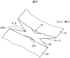
- FIG. 9 shows a stress distribution when the flexible wiring board 20 according to the present invention is curved as shown in FIG.
- the numbers corresponding to the contour lines drawn on the flexible wiring board 20 in FIG. 9 indicate the magnitude of stress, and the unit is MPa.
- the stress distribution in FIG. 9 is substantially different from the cases in FIGS. 7 and 8 and is almost zero. That is, there is no region where a stress larger than 3 MPa occurs.
- the flexible wiring board 20 of the present invention is hardly stressed due to the bending of the display panel 10. However, no complicated stress is generated, and it can be considered as if the flat flexible wiring board 20 is bent. As described above, the reason why the stress can be reduced in the flexible wiring board 20 of the present invention is as described in FIG. In other words, the existence of the delta cuts 201 and 202 has a great influence.
- FIG. 10 is a plan view of an ordinary flexible wiring board 20.
- a wiring 21 made of copper or the like is patterned on a base material 22 made of a resin such as polyimide.
- a protective film 23 is formed so as to cover the copper wiring 21.
- the protective film 23 may be what is called a solder resist or the like.
- the protective film 23 covers the copper wiring 21 other than the terminal portion connected to the display panel 10 or the wiring substrate 30.
- FIG. 11 is a sectional view taken along the line AA′ of FIG. 12 is a sectional view taken along line BB′ of FIG.
- Copper wirings 21 are formed at a predetermined pitch on a base material 22 such as polyimide.
- a protective film 23 is formed so as to cover the copper wiring 21.
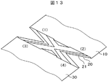
- FIG. 13 shows an example of the flexible wiring board 20 of the present invention.
- an X-shaped flexible wiring board 20 connects the display panel 10 and the wiring board 30.
- the wiring is V-shaped. That is, the wiring 21 connected in the terminal area (1) is curved in a V shape at the center of the flexible wiring board 20 and is connected to the wiring board 30 side in the terminal area (3).
- the wiring 21 connected in the terminal area (2) is curved in a V shape in the center of the flexible wiring board 20 and is connected to the wiring board 30 side in the terminal area (4).
- the terminal area (1) is the first mounting terminal group of the flexible wiring board 20
- the terminal area (2) is the second mounting terminal group of the flexible wiring board 20
- the terminal area (3) is the third mounting terminal of the flexible wiring board 20.
- the terminal group and the terminal area (4) may be restated as the fourth mounting terminal group of the flexible wiring board 20.
- the first to fourth mounting terminal groups of the flexible wiring board 20 are a plurality of terminal groups arranged at intervals in the X direction, and terminal groups corresponding to these mounting terminal groups are also formed on the display panel 10. Has been done.
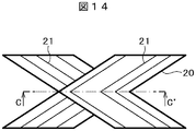
- FIG. 14 is a plan view of a case where the X-shaped flexible wiring board 20 is configured by two V-shaped flexible wiring boards 20 when seen in a plan view.
- a V-shaped wiring 21 is formed on each of the V-shaped flexible wiring boards 20.
- the two V-shaped flexible wiring boards 20 are overlapped with each other in a V-shaped bent portion to form an X-shape as a plane.
- FIG. 15 is a sectional view taken along line CC′ of FIG. Since a high-frequency clock signal and a video signal are supplied to each of the two flexible wiring boards 20, it is necessary to prevent them from interfering with each other. Therefore, in FIG. 15, the conductive films 24 are formed on the opposing surfaces of the flexible wiring boards 20 to prevent interference between the flexible wiring boards 20. In FIG. 15, there is a space between the two flexible wiring boards 20, but this illustrates that there are two flexible wiring boards 20. The space is not always necessary.
- FIG. 16 is a modification of FIGS. 14 and 15. That is, FIG. 16 is a plan view when the configuration of FIG. 13 is configured by two modified V-shaped flexible wiring boards 20.
- the difference between FIG. 16 and FIGS. 14 and 15 is that the two V-shaped flexible wiring boards 20 do not overlap each other in plan view and that the V-shaped flexible wiring boards 20 are bent. That is, the sides facing each other are linear. That is, two V-shaped flexible wiring boards 20 are used as a plane having a V-shaped notch in one of the first directions and a straight side in the other of the first directions.
- An X-shape is formed as a plane in which they are adjacent to each other. By having a straight side on the other side, the degree of freedom in the layout of the wiring 21 is increased.
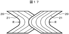
- FIG. 17 is a second modification of FIGS. 14 and 15.
- stress is likely to increase at the V-shaped apex.
- the wiring 21 is bent in a V shape
- the wiring 21 is easily broken at this portion.
- the vicinity of the apex of the V-shape is connected by an arc to relieve the stress in the bent portion.
- the X-shaped flexible wiring board 20 is configured when viewed in a plan view.
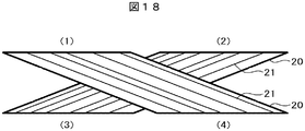
- FIG. 18 shows an example in which two flexible wiring boards 20 each having a parallelogram shape are stacked on top of each other so that the shape of the flexible wiring board 20 as viewed in a plane is X-shaped. In this configuration, since there is no bent portion in each flexible wiring board 20, the risk of disconnection of the wiring 21 is extremely small.
- the terminal area (1) of the display panel 10 and the terminal area (4) of the wiring board 30 are connected, and the terminal area (2) of the display panel 10 and the terminal area (3) of the wiring board 30 are connected.
- the cross-sectional view of the overlapping portion of the two flexible wiring boards 20 in FIG. 18 is the same as FIG.
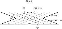
- FIG. 19 shows an example in which the flexible wiring board 20 shown in FIG. 18 is configured by one X-shaped flexible wiring board.
- the outer shape of the flexible wiring board 20 is X-shaped.
- the wiring 212 formed on the flexible wiring board 20 is formed on the back side of the base material 22 as shown by the dotted line in FIG. At the intersection of the wirings 212, one wiring is formed on the base material 22 via the through hole 25 to become the front wiring 211, and after the intersection, the wiring 212 is connected again to the back wiring 212 via the through hole 25. doing.
- FIG. 20 is a sectional view taken along the line DD′ of FIG. 19.
- the back wiring 212 is formed on the lower side of the base material 22.
- the through hole 25 is opened and the wiring 212 on the back side is connected to the wiring 211 on the front side.
- the front wiring 211 is again connected to the back wiring 212 via the through hole 25. Both the front wiring 211 and the back wiring 212 are covered with the protective film 23.
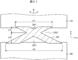
- FIG. 21 shows a modification of the X-shaped flexible wiring board 20.
- FIG. 21 shows that the intersection of X is closer to the display panel 10 than the wiring board 30. That is, y1 ⁇ y2. Also, x1 ⁇ x2.
- x1 ⁇ x2. When the display panel 10 is bent in the direction of the arrow A while the wiring board 30 is kept flat, stress is generated in the flexible wiring board 20, but on the display panel 10 side, this stress becomes smaller as x1 decreases. small.
- the structure of FIG. 21 is advantageous in that the display panel 10 is prevented from being stressed.
- the flexible wiring board 20 When the flexible wiring board 20 is bent and the wiring board 30 is arranged on the back surface of the display panel 10, the flexible wiring board 20 is bent at the intersection, that is, the position y1 from the upper portion of the flexible wiring board 20. Since y1 is smaller than y2, the flexible wiring board 20 is bent at a radius smaller than (y1+y2)/2, which is half the length in the y direction.
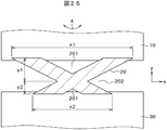
- FIG. 22 is a cross-sectional view when the flexible wiring board 20 is bent on the back surface of the display panel 10.
- the flexible wiring board 20 can be curved with a small radius, so that d1 in FIG. 22 can be reduced. That is, it is possible to reduce the outer shape of the display device, and in particular, it is possible to realize the narrow frame of the bent region of the flexible wiring board 20.
- FIG. 23 shows an example in which the driver IC 15 is arranged on the display panel 10 side. Since the width x1 on the upper side of the flexible wiring board 20 is small, only one driver IC 15 is covered in FIG.
- FIG. 24 is an example in which two driver ICs 15 are arranged on the display panel 10 corresponding to the terminal areas of the flexible wiring board 20. In the display panel 10, in particular, the wirings 11 are often densely packed on the side edges. Therefore, by arranging the driver ICs 15 as shown in FIG. 24, it is possible to prevent the wiring pitch from becoming extremely small especially in the diagonal wirings. Can be done.
- FIG. 25 shows another modification of the X-shaped flexible wiring board 20.
- the feature of FIG. 25 is that the X-shaped intersection is closer to the wiring substrate 30 than the display panel 10. That is, y1>y2. Also, x1>x2.
- the configuration of FIG. 25 is not suitable for a configuration in which the display panel is curved with a small radius of curvature.
- the flexible wiring board 20 When the wiring board 30 is bent to the rear surface of the display panel 10, the flexible wiring board 20 is bent at the intersection, that is, the position y1 from the upper portion of the flexible wiring board 20.
- y1 is larger than y2.
- the flexible wiring board 20 is bent at a radius larger than (y1+y2)/2, which is half the length in the y direction.
- FIG. 26 is a cross-sectional view when the flexible wiring board 20 is bent on the back surface of the display panel 10.
- the flexible wiring board 20 is curved with a relatively large radius. That is, d2 in FIG. 26 is larger than d1 in FIG. That is, the configuration of FIG. 25 is not suitable for making the outer shape of the display device small.
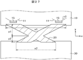
- FIG. 27 shows a case where the driver IC 15 is arranged on the display panel 10 side in the configuration of FIG.
- the driver IC 15 can be arranged further outside than in the case of FIG.
- the wirings 11 are often concentrated on the sides of the side. Therefore, by arranging the driver ICs 15 outside, as shown in FIG. 27, the wiring pitch is prevented from becoming extremely small. You can That is, in FIG. 27, the wiring angle ⁇ 2 can be made smaller than the wiring angle ⁇ 1 in FIG. Therefore, the pitch of the diagonal wiring 11 can be made larger, and the layout of the wiring 11 can be afforded.
- the driver IC 15 As the driver IC 15 described above, a configuration called COG (Chip On Glass) mounted on the display panel 10 was described.
- the relationship between the driver IC and the flexible wiring board is not limited to this structure, and may be a structure called COF (Chip On Film) in which the driver IC 15 is mounted on the X-shaped flexible wiring board 20 of the present invention.
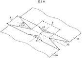
- FIG. 28 is a perspective view showing a general shape of the flexible wiring board 20 according to the present invention.
- the flexible wiring board 20 according to the present invention generally has an X shape, but the X shape does not necessarily have to have a configuration in which parallelograms are crossed.
- ⁇ 1 and ⁇ 2 do not necessarily have to have the same value. Both ⁇ 1 and ⁇ 2 can take values of 10 degrees to 80 degrees.
- ⁇ 1+ ⁇ 2 ⁇ 3 it is emphasized that the shape is horizontally long.
- ⁇ 1+ ⁇ 2 can be set in the range of 20° to 90°.
- ⁇ 3 is set to 180 degrees ⁇ 2 ⁇ 1 and ⁇ 4 is set to 180 degrees ⁇ 2 ⁇ 2.
- ⁇ 3 and ⁇ 4 are each set to 90 or more and smaller than 180 degrees.
- the dimension A is increased.
- the stress of the flexible wiring board 20 can be reduced, and the stress on the display panel 10 due to the reaction can be reduced.
- FIG. 29 is a plan view showing still another X shape of the flexible wiring board 20 according to the present invention.
- the feature of FIG. 29 is that the portions of the flexible wiring board 20 that are bent in a V shape in the cuts 201 and 202 are smoothed by the radius of curvature R1 or R2. As a result, it is possible to prevent a large local stress from being generated in the flexible wiring board 20. As a result, disconnection of the wiring 21 in the flexible wiring board 20 can be prevented.
- FIG. 30 is a plan view showing still another shape of the flexible wiring board 20 according to the present invention.
- the characteristic of FIG. 30 is that in the flexible wiring board 20, the notches 26 are formed in the notches 201 and 202 at locations where stress is likely to be applied, and a large local stress is prevented from occurring.
- Another feature of FIG. 30 is that the slit 27 is formed in the central portion of the flexible wiring board 20. The slit 27 relieves the stress when the flexible wiring board 20 is bent to the back surface. Therefore, the stress on the display panel 10 due to the reaction can be relieved.
- FIG. 31 is a plan view showing still another form of the flexible wiring board 20 according to the present invention.
- the feature of FIG. 31 is that the central protruding portion 28 extending in the y direction is present in the central portion of the flexible wiring substrate 20 in the x direction.
- the cut 201 is divided into cuts 203 and 204 by the presence of the central protrusion 28.
- Wiring is also formed on the central protrusion 28 and is connected to the display panel 10 and the wiring board 30. Therefore, the flexible wiring board 20 shown in FIG. 31 is connected to the display panel 10 and the wiring board 30 at three points respectively, so that the flexibility of the wiring 31 can be increased while relaxing the bending stress. Also in the configuration of FIG. 31, the flexibility of the flexible wiring board 20, the occurrence of stress, and the like can be adjusted by the dimension A and the dimension B, which is the same as the flexible wiring board 20 of the other form of the X shape. Is.
Landscapes
- Engineering & Computer Science (AREA)
- Microelectronics & Electronic Packaging (AREA)
- Physics & Mathematics (AREA)
- General Physics & Mathematics (AREA)
- Theoretical Computer Science (AREA)
- Devices For Indicating Variable Information By Combining Individual Elements (AREA)
- Combinations Of Printed Boards (AREA)
- Liquid Crystal (AREA)
- Structure Of Printed Boards (AREA)
- Electroluminescent Light Sources (AREA)
Abstract
表示パネルが第1の方向に湾曲し、表示パネルに接続したフレキシブル配線基板が表示パネルの背面に折り返される表示装置において、フレキシブル配線基板は、表示パネルと第1の領域及び第2の領域で接続し、且つ、配線基板と第3の領域及び第4の領域で接続し、第1の領域と第2の領域、及び、第3の領域と第4の領域とは第1の方向において離れており、フレキシブル配線基板は、第1の領域の外端と第2の領域の外端との間に、第1の方向に幅w1を有し、第3の領域の外端と第4の領域の外端との間に、第1の方向に幅w2を有し、第1の領域と第3の領域の間、及び、第2の領域と第4の領域の間において、第1の方向の幅が最も小さな幅w3を有し、フレキシブル配線基板の第1の配線群は、第1の領域と、第3または第4の領域を接続し、第2の配線群は、第2の領域と第3又は第4の領域を接続する。
Description
本発明は表示装置に係り、特に基板を湾曲して使用することができる表示装置に関する。
また、表示装置やセンサ基板を含め様々な電子機器に係り、特にフレキシブル配線基板を実装する電子機器に関する。
有機EL表示装置やマイクロLED装置などの自発光型表示装置、液晶表示装置などの表示装置は、そのデザイン性や用途により湾曲した形状が求められることがある。さらに表示装置に限らず、タッチパネルや光学センサ等のセンサ基板も組み合わせる機器のデザインに応じて湾曲した形状が求められることも有る。表示装置やセンサ基板の湾曲の方向は、横軸(以後x軸という場合もある)に沿って湾曲する場合と縦軸(以後y軸という場合もある)に沿って湾曲する場合がある。
表示装置やセンサ基板に電源や信号を供給するために、フレキシブル配線基板が使用されるが、表示装置やセンサ基板の外形を大きくしないために、フレキシブル配線基板は折り曲げて使用される場合が多い。このような場合、特許文献1及び2には、フレキシブル配線基板を接続される表示装置の辺に沿って複数配置する構成が記載されている。
また、表示装置を薄くするために、フレキシブル配線基板を折り返して使用される場合が多い。このような場合、フレキシブル配線基板が接続される表示装置の辺が湾曲していると、フレキシブル配線基板は、その折り返し方向に強い曲げストレスをうける。特許文献3には、これを軽減するために、フレキシブル配線基板にスリットを形成する構成が記載されている。
フレキシブル配線基板を折り返して使用するような場合、フレキシブル配線基板を接続するとき、他の基板における配線とのショート等の問題が生ずることがある。この対策として特許文献4には、フレキシブル配線基板の表側と裏側に接続端子と配線を分けて形成する構成が記載されている。
湾曲した辺に沿ってフレキシブル配線基板を接続し、かつ、このフレキシブル配線基板を折り曲げたり、折り返したりして使用すると、フレキシブル配線基板は複雑な方向のストレスをうける。フレキシブル配線基板がストレスを受けるということは、反作用によって、フレキシブル配線基板が接続されている部分の表示装置もストレスを受けるということである。
基板にガラスを使用した表示装置やセンサ基板では、湾曲可能とするには、ガラス基板を薄くする必要がある。このような場合、フレキシブル配線基板を湾曲した場合のストレスによって、ガラス基板が破損する危険がある。また、基板に樹脂を使用する場合は、フレキシブル配線基板を湾曲した場合のストレスによって、フレキシブル配線基板の接続部分において、表示装置やセンサ基板の曲率が変化してしまう危険がある。
フレキシブル配線基板を複数に分割して接続することによって、ストレスは軽減することが出来るが、湾曲した部分の曲率半径によっては、多数のフレキシブル配線基板に分割しなければならないという問題を生ずる。また、フレキシブル配線基板にスリットを形成する場合、フレキシブル配線基板内に形成される配線レイアウト等との関係で十分なストレス緩和を得られない場合が多い。
本発明の課題は、表示装置やセンサ基板の湾曲した辺にフレキシブル配線基板を接続し、このフレキシブル配線基板を折り曲げたり、折り返したりする場合にも、ストレスが大きくならない構成を実現し、色々な使用方法に対応することが出来る表示装置を実現することである。
本発明は上記課題を克服するものであり、代表的な手段は次のとおりである。
(1)平面視において、X形状を有するフレキシブル配線基板を備えた、電子機器。
(2)第1の方向に延在する第1の辺を有する表示パネルと、
第1の方向に延在する第2の辺を有する配線基板と、
前記表示パネルと前記配線基板を前記第1の方向と交差する方向である第2の方向に接続するフレキシブル配線基板を備えた表示装置であって、
前記フレキシブル配線基板は、前記表示パネルと第1の領域及び第2の領域で接続し、前記第1の領域と前記第2の領域は前記第1の方向において離れており、
前記フレキシブル配線基板は、前配線基板と第3の領域及び第4の領域で接続し、前記第3の領域と前記第4の領域は前記第1の方向において離れており、
前記フレキシブル配線は、前記第1の方向若しくは前記第2の方向に斜めに交差する方向に延出する2つの配線群を有し、
前記2つの配線群の一つである第1配線群は、前記第1の領域と前記第3の領域若しくは前記第4の領域の一方とを接続し、
前記2つの配線群のひとつである第2配線群は、前記第2領域と前記第4領域若しくは前記第3領域の他方とを接続し、
前記フレキシブル配線基板は、前記第1の領域の外端と前記第2の領域の外端との間に、前記第1の方向に幅w1を有しており、
前記フレキシブル配線基板は、前記第3の領域の外端と前記第4の領域の外端との間に、前記第1の方向に幅w2を有しており、
前記フレキシブル配線基板は、前記第1の領域と前記第3の領域の間、及び、前記第2の領域と前記第4の領域の間において、前記第1の方向の幅が最も小さな幅w3を有することを特徴とする表示装置。
(3)第1の方向に延在する第1の辺を有する表示パネルと、
第1の方向に延在する第2の辺を有する配線基板と、
前記表示パネルと前記配線基板を前記第1の方向と交差する方向である第2の方向に接続する第1のフレキシブル配線基板と第2のフレキシブル配線基板を備えた表示装置であって、
前記第1のフレキシブル配線基板は、前記表示パネルと第1の領域で接続し、かつ、前記配線基板と第3の領域で接続し、前記第1の領域と前記第3の領域は第1の配線群によって接続し、
前記第2のフレキシブル配線基板は、前記表示パネルと第2の領域で接続し、かつ、前記配線基板と第4の領域で接続し、前記第2の領域と前記第4の領域は第2の配線群によって接続し、
前記第1の配線群は、前記第1の領域と前記第3の領域の間において、前記第1の方向に頂点を有する第1のV字型の配線形状であり、
前記第2の配線群は、前記第2の領域と前記第4の領域の間において、前記第1の配線群と反対側に頂点を有する第2のV字型の配線形状であり、
前記第1のフレキシブル配線基板と前記第2のフレキシブル配線基板は、前記第1のV字型配線及び前記第2のV字型配線の部分においてオーバーラップしており、
前記第1のフレキシブル配線基板と前記第2のフレキシブル配線基板の組み合わせは、
平面で視て、前記第1の領域と前記第2の領域は離れており、かつ、前記第1の領域と前記第2の領域の間には隙間が存在し、
平面で視て、前記第3の領域と前記第4の領域は離れており、かつ、前記第3の領域と前記第4の領域の間には隙間が存在し、
前記第1の領域の外端と前記第2の領域の外端との間は、前記第1の方向に幅w1であり、
前記第3の領域の外端と前記第4の領域の外端との間は、前記第1の方向に幅w2であり、
平面で視て、前記オーバーラップした部分において、前記第1の方向の幅が最も小さくなっている幅w3を有することを特徴とする表示装置。
(4)第1の方向に延在する第1の辺を有する表示パネルと、
第1の方向に延在する第2の辺を有する配線基板と、
前記表示パネルと前記配線基板を前記第1の方向と交差する方向である第2の方向に接続する第1のフレキシブル配線基板と第2のフレキシブル配線基板を備えた表示装置であって、
前記第1のフレキシブル配線基板は、前記表示パネルと第1の領域で接続し、かつ、前記配線基板と第4の領域で接続し、前記第1の領域と前記第4の領域は第1の配線群によって接続し、
前記第2のフレキシブル配線基板は、前記表示パネルと第2の領域で接続し、かつ、前記配線基板と第3の領域で接続し、前記第2の領域と前記第3の領域は第2の配線群によって接続し、
前記第1の配線群は、前記第1の領域と前記第4の領域の間において、斜め方向に直線状に延在し、
前記第2の配線群は、前記第2の領域と前記第3の領域の間において、前記第1の配線群と逆の傾斜を持って斜め方向に直線状に延在し、
前記第1のフレキシブル配線基板と前記第2のフレキシブル配線基板は、前記第1の領域と前記第4の領域の間、及び、前記第2の領域と前記第3の領域の間において、交差するようにオーバーラップしており、
前記第1のフレキシブル配線基板と前記第2のフレキシブル配線基板の組み合わせは、
平面で視て、前記第1の領域と前記第2の領域は離れており、かつ、前記第1の領域と前記第2の領域の間には隙間が存在し、
平面で視て、前記第3の領域と前記第4の領域は離れており、かつ、前記第3の領域と前記第4の領域の間には隙間が存在し、
前記第1の領域の外端と前記第2の領域の外端との間は、前記第1の方向に幅w1であり、
前記第3の領域の外端と前記第4の領域の外端との間は、前記第1の方向に幅w2であり、
平面で視て、前記オーバーラップした部分において、前記第1の方向に最も小さい幅w3を有することを特徴とする表示装置。
第1の方向に延在する第2の辺を有する配線基板と、
前記表示パネルと前記配線基板を前記第1の方向と交差する方向である第2の方向に接続するフレキシブル配線基板を備えた表示装置であって、
前記フレキシブル配線基板は、前記表示パネルと第1の領域及び第2の領域で接続し、前記第1の領域と前記第2の領域は前記第1の方向において離れており、
前記フレキシブル配線基板は、前配線基板と第3の領域及び第4の領域で接続し、前記第3の領域と前記第4の領域は前記第1の方向において離れており、
前記フレキシブル配線は、前記第1の方向若しくは前記第2の方向に斜めに交差する方向に延出する2つの配線群を有し、
前記2つの配線群の一つである第1配線群は、前記第1の領域と前記第3の領域若しくは前記第4の領域の一方とを接続し、
前記2つの配線群のひとつである第2配線群は、前記第2領域と前記第4領域若しくは前記第3領域の他方とを接続し、
前記フレキシブル配線基板は、前記第1の領域の外端と前記第2の領域の外端との間に、前記第1の方向に幅w1を有しており、
前記フレキシブル配線基板は、前記第3の領域の外端と前記第4の領域の外端との間に、前記第1の方向に幅w2を有しており、
前記フレキシブル配線基板は、前記第1の領域と前記第3の領域の間、及び、前記第2の領域と前記第4の領域の間において、前記第1の方向の幅が最も小さな幅w3を有することを特徴とする表示装置。
(3)第1の方向に延在する第1の辺を有する表示パネルと、
第1の方向に延在する第2の辺を有する配線基板と、
前記表示パネルと前記配線基板を前記第1の方向と交差する方向である第2の方向に接続する第1のフレキシブル配線基板と第2のフレキシブル配線基板を備えた表示装置であって、
前記第1のフレキシブル配線基板は、前記表示パネルと第1の領域で接続し、かつ、前記配線基板と第3の領域で接続し、前記第1の領域と前記第3の領域は第1の配線群によって接続し、
前記第2のフレキシブル配線基板は、前記表示パネルと第2の領域で接続し、かつ、前記配線基板と第4の領域で接続し、前記第2の領域と前記第4の領域は第2の配線群によって接続し、
前記第1の配線群は、前記第1の領域と前記第3の領域の間において、前記第1の方向に頂点を有する第1のV字型の配線形状であり、
前記第2の配線群は、前記第2の領域と前記第4の領域の間において、前記第1の配線群と反対側に頂点を有する第2のV字型の配線形状であり、
前記第1のフレキシブル配線基板と前記第2のフレキシブル配線基板は、前記第1のV字型配線及び前記第2のV字型配線の部分においてオーバーラップしており、
前記第1のフレキシブル配線基板と前記第2のフレキシブル配線基板の組み合わせは、
平面で視て、前記第1の領域と前記第2の領域は離れており、かつ、前記第1の領域と前記第2の領域の間には隙間が存在し、
平面で視て、前記第3の領域と前記第4の領域は離れており、かつ、前記第3の領域と前記第4の領域の間には隙間が存在し、
前記第1の領域の外端と前記第2の領域の外端との間は、前記第1の方向に幅w1であり、
前記第3の領域の外端と前記第4の領域の外端との間は、前記第1の方向に幅w2であり、
平面で視て、前記オーバーラップした部分において、前記第1の方向の幅が最も小さくなっている幅w3を有することを特徴とする表示装置。
(4)第1の方向に延在する第1の辺を有する表示パネルと、
第1の方向に延在する第2の辺を有する配線基板と、
前記表示パネルと前記配線基板を前記第1の方向と交差する方向である第2の方向に接続する第1のフレキシブル配線基板と第2のフレキシブル配線基板を備えた表示装置であって、
前記第1のフレキシブル配線基板は、前記表示パネルと第1の領域で接続し、かつ、前記配線基板と第4の領域で接続し、前記第1の領域と前記第4の領域は第1の配線群によって接続し、
前記第2のフレキシブル配線基板は、前記表示パネルと第2の領域で接続し、かつ、前記配線基板と第3の領域で接続し、前記第2の領域と前記第3の領域は第2の配線群によって接続し、
前記第1の配線群は、前記第1の領域と前記第4の領域の間において、斜め方向に直線状に延在し、
前記第2の配線群は、前記第2の領域と前記第3の領域の間において、前記第1の配線群と逆の傾斜を持って斜め方向に直線状に延在し、
前記第1のフレキシブル配線基板と前記第2のフレキシブル配線基板は、前記第1の領域と前記第4の領域の間、及び、前記第2の領域と前記第3の領域の間において、交差するようにオーバーラップしており、
前記第1のフレキシブル配線基板と前記第2のフレキシブル配線基板の組み合わせは、
平面で視て、前記第1の領域と前記第2の領域は離れており、かつ、前記第1の領域と前記第2の領域の間には隙間が存在し、
平面で視て、前記第3の領域と前記第4の領域は離れており、かつ、前記第3の領域と前記第4の領域の間には隙間が存在し、
前記第1の領域の外端と前記第2の領域の外端との間は、前記第1の方向に幅w1であり、
前記第3の領域の外端と前記第4の領域の外端との間は、前記第1の方向に幅w2であり、
平面で視て、前記オーバーラップした部分において、前記第1の方向に最も小さい幅w3を有することを特徴とする表示装置。
以下に実施例を用いて本発明の内容を詳細に説明する。本発明は、液晶表示装置や電気泳動表示装置などの電気光学層を備えた表示装置、有機EL表示装置やマイクロLED表示装置などの自発光型の表示装置をはじめ、種々の表示装置に適応することが出来る。また、詳述はしないが、外付けのタッチセンサや指紋センサ等の各種センサ装置にも適用できる。
さらに、フレキシブル配線基板が実装される、表示装置やセンサ装置以外の他の電子機器にも当然適用できるものである。
以下説明する表示パネルは、センサ装置のセンサ基板、電子機器のフレキシブル配線基板が実装される基板、と置き換えることもできる。
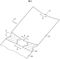
図1は比較例としての表示装置の斜視図である。図1において、表示パネル10は矢印Aのように、x軸方向に曲率半径Rで湾曲している。表示パネル10は液晶表示パネルの場合もあるし、有機EL表示パネルの場合もある。あるいは、湾曲可能なその他の薄型表示パネルであってもよい。湾曲している辺に表示パネルに電源や信号を供給するフレキシブル配線基板20が接続している。フレキシブル配線基板20の他方の端には、配線基板30が接続している。配線基板30は例えばPCB基板であり、剛性があり、かつ、図1の矢印Bで示すように、x軸方向に直線となっている。ただし、配線基板30は表示パネル10の湾曲に沿うように湾曲させたものであっても良い。
したがって、図1のままの状態でも、フレキシブル配線基板20に捩じれ方向のストレスがかかる。図1において、表示装置の外形を小さくし、かつ、表示装置の厚さを小さくするために、フレキシブル配線基板20は矢印Cで示す方向に折り返されることが予定されている。フレキシブル配線基板20が裏側に折り返されるとフレキシブル配線基板20には2方向から曲げ圧力が加わり、複雑で大きなストレスが加わることになる。これら湾曲した表示パネル10に実装されるために生じるフレキシブル配線基板20の湾曲、また捩じれによるストレスにより矢印Cで示す方向にフレキシブル配線基板20を折り曲げることは極めて困難であり、無理矢理折り曲げることは表示パネル10の破壊や、フレキシブル配線基板の多大な変形を引き起こすことが想定される。また、表示パネル10の湾曲した辺に実装されたフレキシブル配線基板20を折り曲げることが仮に出来たとしても、フレキシブル配線基板20にかかるストレスにより、表示パネル10とフレキシブル配線基板20との接続不良を引き起こす可能性も想定される。すなわちフレキシブル配線基板20にかかるストレスにより表示パネル10からフレキシブル配線基板20が剥がれてしまうことになる。
フレキシブル配線基板20は、ポリイミド等の樹脂基材に銅等の配線が施されたものである。基材であるポリイミドは、機械的な強度が大きいので、フレキシブル配線基板20が破壊する危険は小さい。一方、フレキシブル配線基板20にこのようなストレスが加わると、反作用によって、表示パネル10にもストレスがかかる。表示パネル10の基板がガラスで形成されている場合は、湾曲可能とするために、ガラスは0.2mmあるいは、それ以下に薄くなっている。したがって、ガラス基板10が破損する危険が生ずる。表示パネル10の基板が樹脂で形成されている場合は、破壊する危険は小さいが、反作用によって表示パネル10の曲率が変化する。したがって、以後の説明で、フレキシブル配線基板20にかかるストレスの問題は、表示パネル10に係るストレスの問題と言い換えることが出来る。
なお、フレキシブル配線基板20に係るストレスの反作用は、配線基板30にもかかるが、配線基板30は、強度の強い樹脂基板で形成されるので、配線基板30が破壊する危険は非常に小さい。また、曲率の変化が問題になることもない。したがって、以後、反作用という場合は、表示パネル10に発生する反作用であるとして説明する。
図1は、フレキシブル配線基板20にかかるストレスを緩和するために、フレキシブル配線基板20を2つの矩形のフレキシブル配線基板20に分割した場合である。しかし、図1のような構成は、十分なストレス緩和にはならない。特に、フレキシブル配線基板20を矢印Cのように折り返した場合は、表示パネル10の基板が薄いガラス基板の場合には破損の危険がある。さらにフレキシブル配線基板20も表示パネル10の湾曲に沿って、湾曲されており、折り返すことは極めて困難であり、矢印Cのように折り返した場合には、フレキシブル配線基板に多大な変形を引き起こすことが想定される。
図2はこれを対策した第2の比較例としての表示装置の斜視図である。図2において、表示パネル10、配線基板30は図1で説明したのと同様である。フレキシブル配線基板20は、2つに分割されているが、各々のフレキシブル配線基板20の形状は図1と異なり、平面が砂時計形状である。フレキシブル配線基板20がこのような形状の場合、折り曲げたとき、中央のくびれた部分において、曲げやすくなるので、ストレスは小さくなる。しかし、図2の構成でも、十分なストレス緩和にはならない。
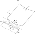
図3は、本発明による表示装置の斜視図である。図3において、表示パネル10、配線基板30は図1で説明したのと同様である。図3におけるフレキシブル配線基板20は、平面がX形状である。すなわち、平面で視て、フレキシブル配線基板20の上下(y方向)、及び左右(x方向)に概略デルタ状の切り込み201及び202が存在している。
フレキシブル配線基板20が表示パネル10と接続する部分は、先端に行くにいしたがって、幅が小さくなっている。したがって、図3の矢印A方向に表示パネル10を湾曲した場合、最も変位が大きくなる先端の幅が小さいために、フレキシブル配線基板20に生ずるストレスは小さい。さらに、x方向中央において、デルタ状の切り込み201の存在によって、フレキシブル配線基板20のy方向の幅が小さくなっているので、x軸方向に湾曲しやすくなっており、さらにストレスが緩和される。逆に表示パネル10に係る反作用も小さい。
また、フレキシブル配線基板20を図3に示すC方向に湾曲あるいは折り返す場合、デルタ状の切り込み202の存在によって、フレキシブル配線基板20の中央部分において、x方向の幅が小さくなっているので、曲げストレスは緩和される。
したがって、図3の構成によれば、A方向の湾曲に対しても、C方向の折り曲げに対しても、フレキシブル配線基板20に発生するストレスは緩和することが出来る。つまり、フレキシブル配線基板20のストレスの反作用によって生ずる表示パネル10へのストレスも緩和させることが出来る。
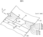
図4乃至図6は、図1乃至図3に対応し、配線基板30を平面に保ったまま、表示パネル10を曲率半径Rによって湾曲させた場合のフレキシブル配線基板20における変位量を示す斜視図である。図4乃至図6におけるフレキシブル配線基板20の幅w3及びの曲率半径Rは同一である。曲率半径Rは、円弧の長さw3が97.6mmとした場合に、矢高が1.6mmとなるような曲率半径Rとなっている。なお、図4乃至図6において、フレキシブル配線基板20の幅w1=36mm、隙間w2=25.6、フレキシブル配線基板20の端部から端部までの幅w3=97.6mmは共通である。また、フレキシブル配線基板20のy方向の長さhは24mmであり、図4乃至図6において共通である。
図4において、w1は各々のフレキシブル配線基板20の幅であり、w2はフレキシブル配線基板20とフレキシブル配線基板20の間隔であり、w3は2枚のフレキシブル配線基板20における外側端部から外側端部までの距離である。図4において、フレキシブル配線基板20に描かれた等高線に対応する数字は、フレキシブル配線基板20が接する平面からのz方向の距離に該当する。
図4に示すように、2枚のフレキシブル配線基板20の、表示パネル10と接続している側の外側端部が最も変位が大きく1.6mmである。そして、変位は、フレキシブル配線基板20が配線基板30と接続している側の内側端部においてゼロに近づくように徐々に小さくなっている。
図5はフレキシブル配線基板20の平面が砂時計形状の場合における、フレキシブル配線基板20の変位を示す図である。図5において、R、w1、w2、w3は図4と同じである。フレキシブル配線基板20に記載された等高線の意味も図4で説明したのと同様である。図5では、砂時計形状特有のくびれが存在しているが、このくびれの量w11は6mmである。
図5におけるフレキシブル配線基板20の変位は、図4の場合と殆ど同じである。すなわち、2枚のフレキシブル配線基板20の、表示パネルと接続している側の外側端部が最も変位が大きく1.6mmである。そして、変位は、フレキシブル配線基板20が配線基板30と接続している側の内側端部においてゼロに近づくように徐々に小さくなっている。
図6は本発明によるフレキシブル配線基板20の場合における、フレキシブル配線基板20の変位を示す図である。図6において、曲率半径Rは図4、図5と同じである。図6において、フレキシブル配線基板20が表示パネルと接続する部分は、デルタ形の切り込み201によって2箇所に分かれており、各々の接続部分のx方向の幅はw1である。また、切り込みのx方向の幅はw2である。そして、フレキシブル配線基板の外端から外端までの幅、すなわち、x方向の幅はw1である。図6において、フレキシブル配線基板20に記載された等高線の意味は図4で説明したのと同様である。
図6におけるフレキシブル配線基板20の変位は、図4及び図5とは大きく異なっている。フレキシブル配線基板20の、表示パネル10と接続している側の外側両端部が最も変位が大きく、1.6mmである。そして、フレキシブル配線基板20の上側の角部における変位は、角の根本に行くにしたがって、小さくなっており、フレキシブル配線基板10の中央部分では、変位はほとんどゼロになっている。
つまり、図6に示す本発明によるフレキシブル配線基板20の場合、フレキシブル配線基板20の中央付近では、曲げ応力はほとんどゼロとなっている。したがって、配線基板30を背面に折り返す場合も、平面のフレキシブル配線基板20を折り返すのと同様な、単純なストレスが発生するのみである。
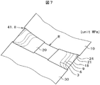
図7乃至図9は、図4乃至図6に対応する、フレキシブル配線基板20におけるストレス分布を示すものである。図7乃至図9は、いわゆるフォンミーゼス応力分布図であり、x方向、y方向、z方向全ての方向の変位を加味した応力であり、応力の方向に関係なく、評価できるようにしたものである。
図7は第1の比較例のフレキシブル配線基板20を図4に示すように湾曲させた場合のストレス分布である。図7におけるフレキシブル配線基板20に描かれた等高線に対応する数字は、ストレスの大きさであり、単位はMPaである。フレキシブル配線基板20のストレスは、表示パネル10と接続している側の外側端部が最も大きく24である。そして、フレキシブル配線基板20が配線基板30側と接続する側における内側端部に向かって徐々に小さくなっている。図7における最大ストレスは41.8である。このストレスは反作用として表示パネル10の端部にも発生している。
図8は第2の比較例のフレキシブル配線基板20を図5に示すように湾曲させた場合のストレス分布である。図8におけるフレキシブル配線基板20に描かれた等高線に対応する数字は、図4で説明したのと同様である。図20において、最大ストレスは48.1であり、これは、砂時計形状のくびれ部で生じている。したがって、このくびれ形状を変えることによって最大ストレスは軽減することが出来る。
図8において、フレキシブル配線基板20が表示パネル10と接続している部分における最大のストレスは9であり、図7の場合と比較して軽減されている。したがって、フレキシブル配線基板に発生するストレスの反作用として、表示パネルに生ずるストレスは図7の場合よりも軽減している。
図9は、本発明によるフレキシブル配線基板20を図6に示すように湾曲させた場合のストレス分布である。図9におけるフレキシブル配線基板20に描かれた等高線に対応する数字は、ストレスの大きさであり、単位はMPaである。図9におけるストレス分布は、図7及び図8の場合と大きく異なっており、殆どゼロである。つまり、3MPaよりも大きなストレスが生ずる領域は存在しない。
図9において、切り込み202の頂点において、局部的に5.8MPaの部分があるが、これは、鋭角になっている部分の特異点であり、この部分を滑らかな曲線でつなぐことによって、この最大ストレスは大幅に小さくなる。また、この最大ストレスは、フレキシブル配線基板20自体に生ずるものであり、表示パネル10に反作用としてストレスを生じさせるものではない。
図9に示すように、本発明のフレキシブル配線基板20によれば、フレキシブル配線基板20には、表示パネル10を湾曲させたことによるストレスは殆ど生じていないので、配線基板30を背面に折り曲げる場合にも、複雑なストレスは発生せず、平らなフレキシブル配線基板20を折り曲げるのと同様に考えることが出来る。このように、本発明のフレキシブル配線基板20において、ストレスを小さくすることが出来る理由は、図3において説明したとおりである。言い換えると、デルタ形の切り込み201、202の存在が大きく影響している。
図10は通常のフレキシブル配線基板20の平面図である。図10において、ポリイミド等の樹脂で形成された基材22の上に、銅等で形成された配線21がパターニングされている。銅配線21を覆って保護膜23が形成されている。保護膜23は、ソルダーレジストなどと呼ばれているものであってもよい。保護膜23は、銅配線21が表示パネル10あるいは配線基板30と接続する端子部分以外を覆っている。
図11は、図10のA-A´断面図である。図12は、図10のB-B´断面図である。ポリイミド等の基材22の上に、銅配線21が所定のピッチで形成されている。銅配線21を覆って保護膜23が形成されている。
図13は、本発明のフレキシブル配線基板20の例である。図13において、X形のフレキシブル配線基板20が表示パネル10と配線基板30を接続している。図13のフレキシブル配線基板20は単層配線になっているので、配線はV字型になっている。すなわち、端子領域(1)で接続した配線21はフレキシブル配線基板20の中央においてV字型に湾曲して端子領域(3)において配線基板30側と接続する。また、端子領域(2)で接続した配線21はフレキシブル配線基板20の中央においてV字型に湾曲して端子領域(4)において配線基板30側と接続する。
また、端子領域(1)をフレキシブル配線基板20の第1実装端子群、端子領域(2)をフレキシブル配線基板20の第2実装端子群、端子領域(3)をフレキシブル配線基板20の第3実装端子群、端子領域(4)をフレキシブル配線基板20の第4実装端子群、と言い換えても良い。フレキシブル配線基板20の第1乃至第4実装端子群は、それぞれX方向に間隔を置いて配置された複数の端子群であり、これら実装端子群にそれぞれ対応する端子群が表示パネル10にも形成されている。
図14は、平面で視てX形のフレキシブル配線基板20を2枚のV字型フレキシブル配線基板20で構成した場合の平面図である。図14において、V字型のフレキシブル配線基板20の各々には、V字型の配線21が形成されている。2枚のV字型のフレキシブル配線基板20は、V字型に屈曲している部分において、重なって、平面としてはX形を形成している。
図15は、図14のC-C´断面図である。2枚のフレキシブル配線基板20の各々には、高周波のクロック信号や映像信号が供給されるので、互いに干渉することを防止する必要がある。そこで、図15では、各々のフレキシブル配線基板20の対向する面に導電膜24を形成することによって、互いのフレキシブル配線基板20間での干渉を防止している。図15では、2枚のフレキシブル配線基板20の間に間隔が存在しているが、これは、2枚のフレキシブル配線基板20だということを描いたものである、間隔はかならずしも必要ではない。
図16は図14及び図15の変形例である。つまり、図16は、図13の構成を、2枚の変形V字型のフレキシブル配線基板20で構成した場合の平面図である。図16が図14、図15と異なる点は、2枚のV字型のフレキシブル配線基板20が平面視においてそれぞれ重なっていない点と、V字型のフレキシブル配線基板20の屈曲している部分において互いに向かい合う辺が直線状になっていることである。すなわち第1方向の一方にV字状の切欠きと、第1方向の他方に直線状の辺を有する平面としてはV字型状のフレキシブル配線基板20を2枚用い、2つのフレキシブル配線基板20同士を隣り合わせ平面としてはX型を形成している。直線状の辺を他方に有することで配線21の引き回しレイアウトの自由度が広がる。
図17は図14、図15の第2の変形例である。図14、図15におけるV字型のフレキシブル配線基板20は、V字型の頂点においてストレスが大きくなりやすい。特に配線21がV字型に屈曲すると、フレキシブル配線基板20を折り曲げた場合、この部分において、配線21が断線しやすい。図17では、V字の頂点付近を円弧で結んで屈曲部のストレスを緩和している。これによって、フレキシブル配線基板20が曲げストレスによって破損すること、あるいは、配線21が断線する危険を防止することが出来る。図17で示す形状であっても平面で視てX形のフレキシブル配線基板20を構成する。
図18は、2枚の平行四辺形の形状をしたフレキシブル配線基板20を互いに重ねあわせることによって、平面で視たフレキシブル配線基板20の形状を、X形に構成した例である。この構成は、各フレキシブル配線基板20において、屈曲部が存在しないので、配線21の断線の危険は非常に小さくなる。図18において、表示パネル10の端子領域(1)と配線基板30の端子領域(4)が接続し、表示パネル10の端子領域(2)と配線基板30の端子領域(3)が接続する。図18における2枚のフレキシブル配線基板20の重なった部分の断面図は図15と同様である。
図19は、図18のフレキシブル配線基板20の構成を1枚のX形フレキシブル配線基板で構成した例である。図19において、フレキシブル配線基板20の外形はX形をしている。フレキシブル配線基板20に形成された配線212は、図19の点線で示すように、基材22の裏側に形成されている。配線212が交差する部分においては、スルーホール25を介して一方の配線が基材22の上に形成されて表側配線211となり、交差後、再び、スルーホール25を介して裏側の配線212と接続している。
図20は、図19のD-D´断面図である。図20において、基材22の下側に裏配線212が形成されている。配線が交差する部分では、スルーホール25を解して、裏側の配線212が表側の配線211に接続している。そして、配線が交差した後、表配線211は、再びスルーホール25を介して裏配線212に接続する。表配線211、裏配線212とも保護膜23で覆われている。
図21はX形フレキシブル配線基板20の変形例である。図21はXの交差部が配線基板30よりも表示パネル10に近いことである。つまり、y1<y2である。また、x1<x2である。配線基板30を平面に保ったまま、表示パネル10を矢印Aの方向に湾曲させた場合、フレキシブル配線基板20にはストレスが発生するが、表示パネル10側では、このストレスは、x1が小さいほど小さい。表示パネル10にストレスがかかることを防止する意味では、図21の構成は有利である。
フレキシブル配線基板20を折り曲げて配線基板30を表示パネル10の背面に配置する場合、フレキシブル配線基板20は交差部、すなわち、フレキシブル配線基板20の上部からy1の位置で曲がることになる。ここでy1はy2よりも小さいので、フレキシブル配線基板20は、y方向の長さの半分である(y1+y2)/2よりも小さな半径で折れ曲がることになる。
図22は、フレキシブル配線基板20を表示パネル10の背面に折り曲げた場合の断面図である。図21の構成であれば、フレキシブル配線基板20は小さな半径で湾曲させることが出来るので、図22におけるd1を小さくすることが出来る。すなわち、表示装置の外形を小さくする、特にフレキシブル配線基板20の折り曲げ領域の狭額縁化を実現することが出来る。
図23は、表示パネル10側にドライバIC15を配置した例である。フレキシブル配線基板20の上側の幅x1が小さいので、図23では、1個のドライバIC15のみでカバーしている。図24は、フレキシブル配線基板20の端子領域に対応して表示パネル10に2個のドライバIC15を配置した例である。表示パネル10においては、特に、サイドの辺において配線11が密集する場合が多いので、図24のようにドライバIC15を配置することによって、特に斜め配線において配線ピッチが極端に小さくなるのを避けることが出来る。
図25はX形フレキシブル配線基板20の他の変形例である。図25の特徴はX形の交差部が表示パネル10よりも配線基板30に近いことである。つまり、y1>y2である。また、x1>x2である。配線基板30を平面に保ったまま、表示パネル10を矢印Aの方向に湾曲させた場合、フレキシブル配線基板20にはストレスが発生するが、表示パネル10側では、このストレスは、x1が大きいほど大きい。したがって、図25の構成は、小さな曲率半径で表示パネルを湾曲させる構成にはむいていない。
配線基板30を表示パネル10の背面に折り曲げる場合、フレキシブル配線基板20は交差部、すなわち、フレキシブル配線基板20の上部からy1の位置で曲がることになる。ここでy1はy2よりも大きい。フレキシブル配線基板20は、y方向の半分の長さである(y1+y2)/2よりも大きな半径で折れ曲がることになる。
図26は、フレキシブル配線基板20を表示パネル10の背面に折り曲げた場合の断面図である。図25の構成の場合、フレキシブル配線基板20は比較的大きな半径で湾曲させることになる。つまり、図26におけるd2は図22におけるd1よりも大きくなる。すなわち、図25の構成は、表示装置の外形を小さくしたい場合には向いていない。
図27は、図25の構成において、表示パネル10側にドライバIC15を配置した場合である。図27では、図24の場合に比較して、ドライバIC15をより外側に配置することが出来る。表示パネル10においては、特に、サイドの辺において配線11が密集する場合が多いので、図27に示すように、ドライバIC15をより外側に配置することによって、配線ピッチが極端に小さくなることを避けることが出来る。すなわち、図27において、配線角度η2を図24における配線角度η1よりも小さくできる。したがって、斜め配線11のピッチをより大きくとることが出来、配線11のレイアウトに余裕をとることが出来る。
上述のドライバIC15については表示パネル10に実装されたCOG(Chip On Glass)と言われる構成について説明を行った。しかしながらドライバICとフレキシブル配線基板との関係はこの構造に限らず、本発明のX形状のフレキシブル配線基板20にドライバIC15が実装されるCOF(Chip On Film)と言われる構成であっても良い。
図28は、本発明によるフレキシブル配線基板20の一般的な形状を示す斜視図である。本発明によるフレキシブル配線基板20は、一般的な形状はX形であるが、このX形は、かならずしも、平行四辺形がクロスした構成である必要はない。
図28において、θ1とθ2は必ずしも同じ値である必要はない。θ1もθ2も各々10度乃至80度の値をとることが出来る。ここで、θ1+θ2<θ3である場合は、横長形状であることが強調される。θ1+θ2は20度乃至90度の範囲で設定することが出来る。また、θ3は、180度-2×θ1、θ4は、180度-2×θ2で設定することが望ましい。θ3及びθ4は、各々、90以上で、180度よりも小さい範囲で設定される。
表示パネル10を図1乃至図3で説明したように湾曲させ、かつ、フレキシブル配線基板20を背面に折り曲げるようなとき、図28に示すようなフレキシブル配線基板20の形状の場合、寸法Aを大きく、寸法Bを小さくすることによって、フレキシブル配線基板20の応力を軽減でき、反作用による表示パネル10への応力を軽減することが出来る。
図29は、本発明によるフレキシブル配線基板20のさらに他のX形状を示す平面図である。図29の特徴は、フレキシブル配線基板20において、切り込み201及び202内においてV字型に屈曲している部分を曲率半径R1またはR2によって、滑らかにしたものである。これによって、フレキシブル配線基板20において局部的に大きなストレスが発生することを防止することが出来る。ひいては、フレキシブル配線基板20内での配線21の断線も防止することが出来る。
図30は、本発明によるフレキシブル配線基板20のさらに他の形状を示す平面図である。図30の特徴は、フレキシブル配線基板20において、切り込み201及び202内において、ストレスのかかりやすい場所にノッチ26を形成し、局部的に大きなストレスが発生することを防止した構成である。図30の他の特徴は、フレキシブル配線基板20の中央部において、スリット27を形成している点である。このスリット27は、フレキシブル配線基板20を背面に折り曲げたときのストレスを緩和するものである。したがって、反作用による表示パネル10へのストレスも緩和することが出来る。
図31は、本発明によるフレキシブル配線基板20のさらに他の形態を示す平面図である。図31の特徴は、フレキシブル配線基板20のx方向の中心部にy方向に延在する中央突起部28が存在することである。切り込み201は、中央突起部28の存在によって、切り込み203と204に分割されている。
中央突起部28にも配線は形成されており、表示パネル10及び配線基板30と接続している。したがって、図31のフレキシブル配線基板20は、表示パネル10及び配線基板30と各々3箇所で接続しており、曲げストレスを緩和しつつ、配線31の自由度を増すことが出来る。図31の構成においても、フレキシブル配線基板20の湾曲のし易さ、ストレスの発生等は、寸法A及び寸法Bによって調整可能であることは、X形の他の形態のフレキシブル配線基板20と同じである。
10…表示パネル、11…配線、 15…ドライバIC、 20…フレキシブル配線基板、 21…配線、 22…基材、 23…保護膜、 24…シールド用導電膜、 25…スルーホール、 26…ノッチ、 27…スリット、 28…中央突起部、 30…配線基板、 31…配線、 201…切り込み、 202…切り込み、 203…切り込み、 204…切り込み、 211…表配線、 212…裏配線
Claims (18)
- 平面視において、X形状を有するフレキシブル配線基板を備えた、電子機器。
- さらに、第1の方向に延在する第1の辺を有する第1基板と、を備え、
前記第1基板及び前記第1基板の前記第1の辺は前記第1の方向に沿って湾曲しており、
前記フレキシブル配線基板は、前記第1の方向に交差する第2の方向において、前記第2の方向の一方側に第1の実装端子群と第2の実装端子群と、前記第2の方向の他方側に第3の実装端子群と第4の実装端子群と、を有し、
前記第1の実装端子群及び前記第2の実装端子群は、前記第1基板の前記第1の辺に実装される、請求項1に記載の電子機器。 - さらに、第2基板を備え、
前記第3の実装端子群と、前記第4の実装端子群は、前記第2基板に実装される、請求項2に記載の電子機器。 - 第1の方向に延在する第1の辺を有する表示パネルと、
第1の方向に延在する第2の辺を有する配線基板と、
前記表示パネルと前記配線基板を前記第1の方向と交差する方向である第2の方向に接続するフレキシブル配線基板を備えた表示装置であって、
前記フレキシブル配線基板は、前記表示パネルと第1の領域及び第2の領域で接続し、前記第1の領域と前記第2の領域は前記第1の方向において離れており、
前記フレキシブル配線基板は、前配線基板と第3の領域及び第4の領域で接続し、前記第3の領域と前記第4の領域は前記第1の方向において離れており、
前記フレキシブル配線は、前記第1の方向若しくは前記第2の方向に斜めに交差する方向に延出する2つの配線群を有し、前記2つの配線群の一つである第1配線群は、前記第1の領域と前記第3の領域若しくは前記第4の領域の一方とを接続し、前記2つの配線群のひとつである第2配線群は、前記第2領域と前記第4領域若しくは前記第3領域の他方とを接続し、
前記フレキシブル配線基板は、前記第1の領域の外端と前記第2の領域の外端との間に、前記第1の方向に幅w1を有しており、
前記フレキシブル配線基板は、前記第3の領域の外端と前記第4の領域の外端との間に、前記第1の方向に幅w2を有しており、
前記フレキシブル配線基板は、前記第1の領域と前記第3の領域の間、及び、前記第2の領域と前記第4の領域の間において、前記第1の方向の幅が最も小さな幅w3を有することを特徴とする表示装置。 - 前記フレキシブル配線基板は前記第1の幅w1と前記第2の幅w2が等しいことを特徴とする請求項4に記載の表示装置。
- 前記フレキシブル配線基板が前記第1の方向に最も小さな幅w3を有する部分は、前記第2の方向において、前記第1の領域および前記第3の領域の間の中央部分、または、前記第2の領域および前記第4の領域の間の中央部分に存在することを特徴とする請求項4に記載の表示装置。
- 前記フレキシブル配線基板は前記第1の幅w1が前記第2の幅w2よりも小さいことを特徴とする請求項4に記載の表示装置。
- 前記フレキシブル配線基板が前記第1の方向に最も小さな幅w3を有する部分は、前記第2の方向において、前記配線基板よりも前記表示パネルに近い部分に存在することを特徴とする請求項4に記載の表示装置。
- 前記第1の配線群は、前記第1の領域と前記第3の領域とを接続し、前記第2の配線群は前記第2の領域と前記第4の領域とを接続し、
前記第1の配線群は、前記幅w3を有する部分において、略V字型に屈曲し、
前記第2の配線群は、前記幅w3を有する部分において、前記第1の配線群の屈曲する方向とは反対方向に略V字型に屈曲していることを特徴とする請求項4に記載の表示装置。 - 前記第1の配線群は、前記第1の領域と前記第4の領域を接続し、前記第2の配線群は前記第2の領域と前記第3の領域を接続し、
前記第1の配線群と前記第2の配線群が交差する部分において、前記第1の配線群と前記第2の配線群の間には絶縁膜が形成されていることを特徴とする請求項4に記載の表示装置。 - 前記絶縁膜は、前記フレキシブル配線基板の基材であることを特徴とする請求項10に記載の表示装置。
- 前記第1の領域と前記第2の領域の間の第5の領域において、前記フレキシブル配線基板は前記表示パネルと接続し、前記第5の領域と前記第1の領域及び前記第5の領域と前記第2の領域の間には間隔が存在し、
前記第3の領域と前記第4の領域の間の第6の領域において、前記フレキシブル配線基板は前記配線基板と接続し、前記第6の領域と前記第3の領域及び前記第6の領域と前記第4の領域の間には間隔が存在し、
前記第5の領域と前記第6の領域の間には、前記第2の方向に延在する部分を有することを特徴とする請求項4に記載の表示装置。 - 前記表示装置は前記第1の方向に沿って湾曲していることを特徴とする請求項4に記載の表示装置。
- 前記配線基板は、前記フレキシブル配線基板を介して前記表示パネルの背面に折り返されていることを特徴とする請求項13に記載の表示装置。
- 第1の方向に延在する第1の辺を有する表示パネルと、
第1の方向に延在する第2の辺を有する配線基板と、
前記表示パネルと前記配線基板を前記第1の方向と交差する方向である第2の方向に接続する第1のフレキシブル配線基板と第2のフレキシブル配線基板を備えた表示装置であって、
前記第1のフレキシブル配線基板は、前記表示パネルと第1の領域で接続し、かつ、前記配線基板と第3の領域で接続し、前記第1の領域と前記第3の領域は第1の配線群によって接続し、
前記第2のフレキシブル配線基板は、前記表示パネルと第2の領域で接続し、かつ、前記配線基板と第4の領域で接続し、前記第2の領域と前記第4の領域は第2の配線群によって接続し、
前記第1の配線群は、前記第1の領域と前記第3の領域の間において、前記第1の方向に頂点を有する第1のV字型の配線形状であり、
前記第2の配線群は、前記第2の領域と前記第4の領域の間において、前記第1の配線群と反対側に頂点を有する第2のV字型の配線形状であり、
前記第1のフレキシブル配線基板と前記第2のフレキシブル配線基板は、前記第1のV字型配線及び前記第2のV字型配線の部分においてオーバーラップしており、
前記第1のフレキシブル配線基板と前記第2のフレキシブル配線基板の組み合わせは、
平面で視て、前記第1の領域と前記第2の領域は離れており、かつ、前記第1の領域と前記第2の領域の間には隙間が存在し、
平面で視て、前記第3の領域と前記第4の領域は離れており、かつ、前記第3の領域と前記第4の領域の間には隙間が存在し、
前記第1の領域の外端と前記第2の領域の外端との間は、前記第1の方向に幅w1であり、
前記第3の領域の外端と前記第4の領域の外端との間は、前記第1の方向に幅w2であり、
平面で視て、前記オーバーラップした部分において、前記第1の方向の幅が最も小さくなっている幅w3を有することを特徴とする表示装置。 - 前記第1の配線群と前記第2の配線群の間には、導電膜が形成されていることを特徴とする請求項15に記載の表示装置。
- 第1の方向に延在する第1の辺を有する表示パネルと、
第1の方向に延在する第2の辺を有する配線基板と、
前記表示パネルと前記配線基板を前記第1の方向と交差する方向である第2の方向に接続する第1のフレキシブル配線基板と第2のフレキシブル配線基板を備えた表示装置であって、
前記第1のフレキシブル配線基板は、前記表示パネルと第1の領域で接続し、かつ、前記配線基板と第4の領域で接続し、前記第1の領域と前記第4の領域は第1の配線群によって接続し、
前記第2のフレキシブル配線基板は、前記表示パネルと第2の領域で接続し、かつ、前記配線基板と第3の領域で接続し、前記第2の領域と前記第3の領域は第2の配線群によって接続し、
前記第1の配線群は、前記第1の領域と前記第4の領域の間において、斜め方向に直線状に延在し、
前記第2の配線群は、前記第2の領域と前記第3の領域の間において、前記第1の配線群と逆の傾斜を持って斜め方向に直線状に延在し、
前記第1のフレキシブル配線基板と前記第2のフレキシブル配線基板は、前記第1の領域と前記第4の領域の間、及び、前記第2の領域と前記第3の領域の間において、交差するようにオーバーラップしており、
前記第1のフレキシブル配線基板と前記第2のフレキシブル配線基板の組み合わせは、 平面で視て、前記第1の領域と前記第2の領域は離れており、かつ、前記第1の領域と前記第2の領域の間には隙間が存在し、
平面で視て、前記第3の領域と前記第4の領域は離れており、かつ、前記第3の領域と前記第4の領域の間には隙間が存在し、
前記第1の領域の外端と前記第2の領域の外端との間は、前記第1の方向に幅w1であり、
前記第3の領域の外端と前記第4の領域の外端との間は、前記第1の方向に幅w2であり、
平面で視て、前記オーバーラップした部分において、前記第1の方向に最も小さい幅w3を有することを特徴とする表示装置。 - 前記第1の配線群と前記第2の配線群の間には、導電膜が形成されていることを特徴とする請求項17に記載の表示装置。
Priority Applications (6)
| Application Number | Priority Date | Filing Date | Title |
|---|---|---|---|
| JP2020565694A JP7212068B2 (ja) | 2019-01-07 | 2019-12-25 | 表示装置及び電子機器 |
| US17/366,238 US11765829B2 (en) | 2019-01-07 | 2021-07-02 | Display device and electronic device |
| JP2023002223A JP7408851B2 (ja) | 2019-01-07 | 2023-01-11 | 表示装置及び電子機器 |
| US18/364,543 US12010797B2 (en) | 2019-01-07 | 2023-08-03 | Display device and electronic device |
| US18/651,739 US12328818B2 (en) | 2019-01-07 | 2024-05-01 | Display device and electronic device |
| US19/204,861 US20250275060A1 (en) | 2019-01-07 | 2025-05-12 | DISPLAY DEVICE and ELECTRONIC DEVICE |
Applications Claiming Priority (2)
| Application Number | Priority Date | Filing Date | Title |
|---|---|---|---|
| JP2019000514 | 2019-01-07 | ||
| JP2019-000514 | 2019-01-07 |
Related Child Applications (1)
| Application Number | Title | Priority Date | Filing Date |
|---|---|---|---|
| US17/366,238 Continuation US11765829B2 (en) | 2019-01-07 | 2021-07-02 | Display device and electronic device |
Publications (1)
| Publication Number | Publication Date |
|---|---|
| WO2020145147A1 true WO2020145147A1 (ja) | 2020-07-16 |
Family
ID=71521170
Family Applications (1)
| Application Number | Title | Priority Date | Filing Date |
|---|---|---|---|
| PCT/JP2019/050835 Ceased WO2020145147A1 (ja) | 2019-01-07 | 2019-12-25 | 表示装置及び電子機器 |
Country Status (3)
| Country | Link |
|---|---|
| US (4) | US11765829B2 (ja) |
| JP (2) | JP7212068B2 (ja) |
| WO (1) | WO2020145147A1 (ja) |
Cited By (1)
| Publication number | Priority date | Publication date | Assignee | Title |
|---|---|---|---|---|
| CN113176688A (zh) * | 2021-04-26 | 2021-07-27 | Tcl华星光电技术有限公司 | 一种微型发光二极管背光驱动组件和显示面板 |
Families Citing this family (2)
| Publication number | Priority date | Publication date | Assignee | Title |
|---|---|---|---|---|
| TWI832765B (zh) | 2023-05-18 | 2024-02-11 | 頎邦科技股份有限公司 | 薄膜電路板 |
| CN118298725A (zh) * | 2024-03-29 | 2024-07-05 | 京东方科技集团股份有限公司 | 显示模组及显示装置 |
Citations (3)
| Publication number | Priority date | Publication date | Assignee | Title |
|---|---|---|---|---|
| KR20070116371A (ko) * | 2006-06-05 | 2007-12-10 | 삼성전자주식회사 | 연성인쇄회로 및 그 제조 방법, 이를 구비하는 표시 장치 |
| JP2009168904A (ja) * | 2008-01-11 | 2009-07-30 | Sharp Corp | 表示装置 |
| JP2019184755A (ja) * | 2018-04-06 | 2019-10-24 | シャープ株式会社 | 表示装置 |
Family Cites Families (8)
| Publication number | Priority date | Publication date | Assignee | Title |
|---|---|---|---|---|
| JP2820965B2 (ja) | 1989-08-04 | 1998-11-05 | 株式会社リコー | 曲面液晶表示装置 |
| JP2875076B2 (ja) * | 1990-11-29 | 1999-03-24 | 三井化学株式会社 | フレキシブル配線基板 |
| JP4306623B2 (ja) * | 2005-02-25 | 2009-08-05 | セイコーエプソン株式会社 | 表示パネル、表示装置、および移動体の表示モジュール |
| JP5567362B2 (ja) | 2010-02-16 | 2014-08-06 | セイコーインスツル株式会社 | 表示装置及び電子機器 |
| KR102173356B1 (ko) | 2013-12-31 | 2020-11-03 | 엘지디스플레이 주식회사 | 곡면표시장치 |
| KR102355256B1 (ko) * | 2015-01-22 | 2022-01-25 | 삼성디스플레이 주식회사 | 표시 장치 |
| KR20160095311A (ko) * | 2015-02-02 | 2016-08-11 | 삼성디스플레이 주식회사 | 유기 발광 표시 장치 |
| JP2018073705A (ja) | 2016-11-01 | 2018-05-10 | 三洋電機株式会社 | 電源装置及びこれを備える車両並びに電源装置の製造方法 |
-
2019
- 2019-12-25 WO PCT/JP2019/050835 patent/WO2020145147A1/ja not_active Ceased
- 2019-12-25 JP JP2020565694A patent/JP7212068B2/ja active Active
-
2021
- 2021-07-02 US US17/366,238 patent/US11765829B2/en active Active
-
2023
- 2023-01-11 JP JP2023002223A patent/JP7408851B2/ja active Active
- 2023-08-03 US US18/364,543 patent/US12010797B2/en active Active
-
2024
- 2024-05-01 US US18/651,739 patent/US12328818B2/en active Active
-
2025
- 2025-05-12 US US19/204,861 patent/US20250275060A1/en active Pending
Patent Citations (3)
| Publication number | Priority date | Publication date | Assignee | Title |
|---|---|---|---|---|
| KR20070116371A (ko) * | 2006-06-05 | 2007-12-10 | 삼성전자주식회사 | 연성인쇄회로 및 그 제조 방법, 이를 구비하는 표시 장치 |
| JP2009168904A (ja) * | 2008-01-11 | 2009-07-30 | Sharp Corp | 表示装置 |
| JP2019184755A (ja) * | 2018-04-06 | 2019-10-24 | シャープ株式会社 | 表示装置 |
Cited By (1)
| Publication number | Priority date | Publication date | Assignee | Title |
|---|---|---|---|---|
| CN113176688A (zh) * | 2021-04-26 | 2021-07-27 | Tcl华星光电技术有限公司 | 一种微型发光二极管背光驱动组件和显示面板 |
Also Published As
| Publication number | Publication date |
|---|---|
| US20210337667A1 (en) | 2021-10-28 |
| US12010797B2 (en) | 2024-06-11 |
| US11765829B2 (en) | 2023-09-19 |
| US12328818B2 (en) | 2025-06-10 |
| JP7212068B2 (ja) | 2023-01-24 |
| US20250275060A1 (en) | 2025-08-28 |
| JP7408851B2 (ja) | 2024-01-05 |
| JPWO2020145147A1 (ja) | 2021-11-04 |
| US20240284595A1 (en) | 2024-08-22 |
| JP2023052311A (ja) | 2023-04-11 |
| US20230380063A1 (en) | 2023-11-23 |
Similar Documents
| Publication | Publication Date | Title |
|---|---|---|
| JP7408851B2 (ja) | 表示装置及び電子機器 | |
| US9560761B2 (en) | Curved display | |
| EP3201964B1 (en) | Flexible display device with reduced bend stress wires | |
| CN106158817B (zh) | 薄膜覆晶封装结构及封装模块 | |
| CN120406011A (zh) | 显示面板和包括显示面板的显示设备 | |
| US11815955B2 (en) | Display device, flexible wiring board, and manufacturing method of display device | |
| US20220132667A1 (en) | Electronic device | |
| US9059162B2 (en) | Chip on film (COF) substrate, COF package and display device including the same | |
| CN112164316B (zh) | 可折叠显示装置 | |
| JP7607693B2 (ja) | フレキシブル回路基板 | |
| US7663062B1 (en) | Flexible circuit board | |
| US11563036B2 (en) | Array substrate and fabrication method thereof, display panel and display module | |
| WO2011070701A1 (ja) | 駆動装置、表示パネルモジュール、表示装置および駆動装置の製造方法 | |
| CN119451489A (zh) | 显示装置 | |
| JP2018066923A (ja) | 電気光学表示装置 | |
| CN107889342B (zh) | 一种柔性印刷电路板、显示面板和显示装置 | |
| CN110320716A (zh) | 柔性布线板及显示装置 | |
| CN112466216A (zh) | 柔性线路板、曲面显示模组和曲面显示装置 | |
| CN109935572A (zh) | 电子装置 | |
| CN107871758A (zh) | 显示装置 | |
| WO2018029857A1 (ja) | 表示パネル及び表示装置 | |
| CN120048190B (zh) | 显示面板及显示装置 | |
| CN117518546A (zh) | 液晶显示装置 | |
| WO2016171058A1 (ja) | センサシートモジュール | |
| CN116312253A (zh) | 显示装置及其制造方法 |
Legal Events
| Date | Code | Title | Description |
|---|---|---|---|
| 121 | Ep: the epo has been informed by wipo that ep was designated in this application |
Ref document number: 19908205 Country of ref document: EP Kind code of ref document: A1 |
|
| ENP | Entry into the national phase |
Ref document number: 2020565694 Country of ref document: JP Kind code of ref document: A |
|
| NENP | Non-entry into the national phase |
Ref country code: DE |
|
| 122 | Ep: pct application non-entry in european phase |
Ref document number: 19908205 Country of ref document: EP Kind code of ref document: A1 |