WO2020145044A1 - 露光装置 - Google Patents
露光装置 Download PDFInfo
- Publication number
- WO2020145044A1 WO2020145044A1 PCT/JP2019/049137 JP2019049137W WO2020145044A1 WO 2020145044 A1 WO2020145044 A1 WO 2020145044A1 JP 2019049137 W JP2019049137 W JP 2019049137W WO 2020145044 A1 WO2020145044 A1 WO 2020145044A1
- Authority
- WO
- WIPO (PCT)
- Prior art keywords
- exposure
- optical system
- substrate
- exposed
- exposure apparatus
- Prior art date
- Legal status (The legal status is an assumption and is not a legal conclusion. Google has not performed a legal analysis and makes no representation as to the accuracy of the status listed.)
- Ceased
Links
Images


Classifications
-
- G—PHYSICS
- G03—PHOTOGRAPHY; CINEMATOGRAPHY; ANALOGOUS TECHNIQUES USING WAVES OTHER THAN OPTICAL WAVES; ELECTROGRAPHY; HOLOGRAPHY
- G03F—PHOTOMECHANICAL PRODUCTION OF TEXTURED OR PATTERNED SURFACES, e.g. FOR PRINTING, FOR PROCESSING OF SEMICONDUCTOR DEVICES; MATERIALS THEREFOR; ORIGINALS THEREFOR; APPARATUS SPECIALLY ADAPTED THEREFOR
- G03F7/00—Photomechanical, e.g. photolithographic, production of textured or patterned surfaces, e.g. printing surfaces; Materials therefor, e.g. comprising photoresists; Apparatus specially adapted therefor
- G03F7/70—Microphotolithographic exposure; Apparatus therefor
- G03F7/70058—Mask illumination systems
- G03F7/70191—Optical correction elements, filters or phase plates for controlling intensity, wavelength, polarisation, phase or the like
-
- G—PHYSICS
- G03—PHOTOGRAPHY; CINEMATOGRAPHY; ANALOGOUS TECHNIQUES USING WAVES OTHER THAN OPTICAL WAVES; ELECTROGRAPHY; HOLOGRAPHY
- G03F—PHOTOMECHANICAL PRODUCTION OF TEXTURED OR PATTERNED SURFACES, e.g. FOR PRINTING, FOR PROCESSING OF SEMICONDUCTOR DEVICES; MATERIALS THEREFOR; ORIGINALS THEREFOR; APPARATUS SPECIALLY ADAPTED THEREFOR
- G03F7/00—Photomechanical, e.g. photolithographic, production of textured or patterned surfaces, e.g. printing surfaces; Materials therefor, e.g. comprising photoresists; Apparatus specially adapted therefor
- G03F7/20—Exposure; Apparatus therefor
-
- G—PHYSICS
- G03—PHOTOGRAPHY; CINEMATOGRAPHY; ANALOGOUS TECHNIQUES USING WAVES OTHER THAN OPTICAL WAVES; ELECTROGRAPHY; HOLOGRAPHY
- G03F—PHOTOMECHANICAL PRODUCTION OF TEXTURED OR PATTERNED SURFACES, e.g. FOR PRINTING, FOR PROCESSING OF SEMICONDUCTOR DEVICES; MATERIALS THEREFOR; ORIGINALS THEREFOR; APPARATUS SPECIALLY ADAPTED THEREFOR
- G03F7/00—Photomechanical, e.g. photolithographic, production of textured or patterned surfaces, e.g. printing surfaces; Materials therefor, e.g. comprising photoresists; Apparatus specially adapted therefor
- G03F7/70—Microphotolithographic exposure; Apparatus therefor
- G03F7/70058—Mask illumination systems
- G03F7/70075—Homogenization of illumination intensity in the mask plane by using an integrator, e.g. fly's eye lens, facet mirror or glass rod, by using a diffusing optical element or by beam deflection
-
- G—PHYSICS
- G03—PHOTOGRAPHY; CINEMATOGRAPHY; ANALOGOUS TECHNIQUES USING WAVES OTHER THAN OPTICAL WAVES; ELECTROGRAPHY; HOLOGRAPHY
- G03F—PHOTOMECHANICAL PRODUCTION OF TEXTURED OR PATTERNED SURFACES, e.g. FOR PRINTING, FOR PROCESSING OF SEMICONDUCTOR DEVICES; MATERIALS THEREFOR; ORIGINALS THEREFOR; APPARATUS SPECIALLY ADAPTED THEREFOR
- G03F7/00—Photomechanical, e.g. photolithographic, production of textured or patterned surfaces, e.g. printing surfaces; Materials therefor, e.g. comprising photoresists; Apparatus specially adapted therefor
- G03F7/70—Microphotolithographic exposure; Apparatus therefor
- G03F7/70216—Mask projection systems
- G03F7/70308—Optical correction elements, filters or phase plates for manipulating imaging light, e.g. intensity, wavelength, polarisation, phase or image shift
-
- G—PHYSICS
- G03—PHOTOGRAPHY; CINEMATOGRAPHY; ANALOGOUS TECHNIQUES USING WAVES OTHER THAN OPTICAL WAVES; ELECTROGRAPHY; HOLOGRAPHY
- G03F—PHOTOMECHANICAL PRODUCTION OF TEXTURED OR PATTERNED SURFACES, e.g. FOR PRINTING, FOR PROCESSING OF SEMICONDUCTOR DEVICES; MATERIALS THEREFOR; ORIGINALS THEREFOR; APPARATUS SPECIALLY ADAPTED THEREFOR
- G03F7/00—Photomechanical, e.g. photolithographic, production of textured or patterned surfaces, e.g. printing surfaces; Materials therefor, e.g. comprising photoresists; Apparatus specially adapted therefor
- G03F7/70—Microphotolithographic exposure; Apparatus therefor
- G03F7/70691—Handling of masks or workpieces
- G03F7/70716—Stages
- G03F7/70725—Stages control
Definitions
- the present invention relates to an exposure apparatus.
- a scan-type exposure apparatus which performs relative scanning of the mask and the substrate with respect to a projection optical system to perform exposure.
- the exposure field of view is expanded in the scan direction (scanning direction) by scan exposure, in order to further expand the exposure field of view in the direction intersecting the scanning direction (non-scanning direction), multiple scan exposures are performed.
- An exposure apparatus that overlaps regions in the non-scanning direction is also known.
- the exposure apparatus includes a projection optical system, an illumination optical system that supplies illumination light to the projection optical system, and a scanning stage that relatively scans the substrate to be exposed and the projection optical system in the scanning direction.
- the scanning stage relatively scans the exposed substrate with respect to the projection optical system so as to expose the exposed substrate by overlapping a plurality of scanning exposure fields of the projection optical system.
- the illumination optical system or the projection optical system is configured such that, in the exposure, the exposure amount of a non-overlap portion which is exposed on the exposed substrate without overlap is overexposed on the exposed substrate.
- the illuminance changing member is set to be smaller than the exposure amount of the lap portion.
- FIGS. 4(a1), 4(a2) and 4(a3) are views showing the field on the mask, the field stop in the projection optical system and the field on the substrate in the projection optical system 19c in FIG. 1, respectively.
- FIG. 4(b1), 4(b2) and 4(b3) are views showing the field on the mask, the field stop in the projection optical system and the field on the substrate in the projection optical system 19b in FIG. 1, respectively.
- FIG. 4 is a diagram showing an example of exposure energy irradiated on a substrate and an effective exposure amount of a photosensitive material when the exposure apparatus of the first embodiment scan-exposes the substrate.
- FIG. 5A is a diagram showing an exposure field on the substrate of each projection optical system
- FIG. 5B is a diagram showing an exposure region formed on the substrate 22
- FIG. 5C is a diagram showing irradiation on the substrate.
- FIG. 5D is a diagram showing an example of the integrated exposure amount
- FIG. 5D is a diagram showing an example of the effective exposure amount of the photosensitive material.
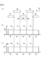
- FIG. 4 is a diagram showing an example of exposure energy irradiated on a substrate and an effective exposure amount of a photosensitive material when the exposure apparatus of the first embodiment scan-exposes the substrate.
- FIG. 7A is a diagram showing the exposure field on the substrate of each projection optical system
- FIG. 7B is a diagram showing an example of the integrated exposure amount irradiated on the substrate
- FIG. 7C is for the photosensitive material. The figure which shows an example of an effective exposure amount.
- FIG. 1 is a side view showing an exposure apparatus 100 of the first embodiment.
- the exposure apparatus 100 includes five projection optical systems 19a to 19e, but FIG. 1 shows only two of them, the projection optical systems 19a and 19b.
- the projection optical systems 19a to 19e are optical systems that form an erect image with a projection magnification (horizontal magnification) of +1.
- the pattern drawn on the mask 15 is a photosensitive material formed on the upper surface of the substrate 22. Exposure transfer.
- the substrate 22 is held by the substrate stage 27 via a substrate holder (not shown).
- the substrate stage 27 can be moved in the Y direction while scanning the substrate stage surface plate 28 in the X direction by a linear motor (not shown) or the like.
- the position of the substrate stage 27 in the X direction is measured by the laser interferometer 25 via the position of the movable mirror 24 attached to the substrate stage 27.
- the position of the substrate stage 27 in the Y direction is also measured by a laser interferometer (not shown).
- the position detection optical system 23 detects the position of an existing pattern such as an alignment mark formed on the substrate 22.
- the mask 15 is held by the mask stage 16.
- the mask stage 16 can be moved in the Y direction while scanning the mask stage surface plate 17 in the X direction by a linear motor or the like (not shown).
- the position of the mask stage 16 in the X direction is measured by the laser interferometer 14 via the position of the movable mirror 13 attached to the mask stage 16.
- the position of the mask stage 16 in the Y direction is also measured by a laser interferometer (not shown).
- a control system controls a linear motor (not shown) and the like based on the measurement values of the laser interferometers 14 and 25 to control the XY positions of the mask stage 16 and the substrate stage 27.
- the control system controls the mask 15 and the substrate 22 with respect to the projection optical systems 19a to 19e while maintaining the imaging relationship of the projection optical systems 19a to 19e.
- the scanning is relatively performed in the X direction at substantially the same speed.
- the direction in which the substrate 22 is scanned (X direction) during exposure is also referred to as “scanning direction” and “scanning direction”.
- a direction (Y direction) included in the plane of the substrate 22 and orthogonal to the X direction is also referred to as a “non-scanning direction” and a “non-scanning direction”.
- the Z direction is a direction orthogonal to the X direction and the Y direction.
- the direction indicated by the arrow is the + direction.
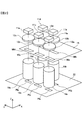
- FIG. 2 is a perspective view showing a portion from the downstream portion of the illumination optical systems ILa to ILe of the exposure apparatus 100 of the first embodiment to the substrate 22.
- first-row projection optical system 19F three projection optical systems 19a, 19c, and 19e (hereinafter, collectively or individually referred to as "first-row projection optical system 19F").
- first-row projection optical system 19F three projection optical systems 19a, 19c, and 19e
- second row projection optical system 19R are arranged side by side in the Y direction, and are arranged more than the first row projection optical system 19F. It is located on the +X side.
- the respective projection optical systems of the projection optical system 19F in the first row are arranged such that their optical axes are apart from each other in the Y direction at a predetermined interval.
- Each optical system of the projection optical system 19R in the second row is arranged similarly to the projection optical system 19F in the first row.
- the projection optical system 19b is arranged so that the position of the optical axis in the Y direction coincides with the approximate center of a straight line connecting the optical axes of the projection optical system 19a and the projection optical system 19c.
- the projection optical system 19d is also arranged in the same manner as the projection optical system 19b.
- the exposure apparatus 100 of the first embodiment includes a plurality of illumination optical systems ILa to ILe corresponding to the respective projection optical systems 19a to 19e.
- the illumination optical system ILa corresponding to the projection optical system 19a includes an input lens 8a, a fly-eye lens 11a, and a condenser lens 12a along the optical axis IXa.
- the other illumination optical systems ILb to ILe also include input lenses 8b to 8e, fly-eye lenses 11b to 11e, and condenser lenses 12b to 12e.
- FIG. 2 shows only the fly-eye lenses 11a to 11e and the condenser lenses 12a to 12e of the illumination optical systems ILa to ILe.
- the projection optical systems 19c to 19e are not shown in FIG. 1, which is a side view, because the projection optical systems 19a and 19b overlap in the X direction.
- the illumination optical systems ILc to ILe are not shown because their positions in the X direction overlap those of the illumination optical systems ILa or ILb.
- Illumination light supplied from a light source 1 such as a lamp passes through a light guide optical system such as an elliptical mirror 2, a bending mirror 3, a relay lens 4, a bending mirror 5, a relay lens 6 and an optical fiber 7, and each illumination optical system ILa.
- the optical fiber 7 splits the illumination light that has entered one incident side 71 into substantially equal parts and emits the branched illumination lights to the five exit sides 72a to 72e.
- the illumination light emitted from each of the five emission sides 72a to 72e of the optical fiber 7 enters the input lenses 8a to 8e in each of the illumination optical systems ILa to ILe. Then, the illumination light is further applied to the illumination areas MIa to MIe on the mask 15 via the fly-eye lenses 11a to 11e and the condenser lenses 12a to 12e.
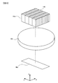
- FIG. 3 is an enlarged perspective view showing, as an example, a fly-eye lens 11c and a condenser lens 12c included in the illumination optical system ILc, and an illumination region MIc on the mask 15.
- the fly-eye lens 11c is formed by arranging a plurality of lens elements 110 similar to the illumination area MIc and having a rectangular cross-sectional shape (shape in the XY plane) long in the Y direction, arranged in the X direction and the Y direction. There is.
- the incident surface (upper surface in FIG. 3, that is, the +Z side surface) of each lens element 110 becomes a conjugate surface with respect to the illumination area MIc on the mask 15 by the optical system including each lens element 110 and the condenser lens 12c. ing.
- each lens element 110 is superimposed and applied to the illumination area MIc on the mask 15. As a result, the illuminance of the illumination light in the illumination area MIc is made substantially uniform.
- the configurations of the other illumination optical systems ILa to ILe except the illumination optical system ILc are the same as those shown in FIG.
- the fly-eye lenses 11a to 11e are an example of an optical integrator that irradiates the illumination areas MIa to MIe with illumination light in a superimposed manner.
- Each of the projection optical systems 19a to 19e is composed of, for example, a two-time imaging type optical system in order to form an erect image.
- a two-time imaging type optical system in order to form an erect image.
- the optical system that constitutes the upper half of each projection optical system 19a to 19e on the intermediate image plane 20 near the middle of the direction (Z direction) of the optical axes PXa to PXe of each projection optical system 19a to 19e, An intermediate image of the pattern of mask 15 is formed.
- the intermediate image is imaged again by the optical system that constitutes the lower half of each projection optical system 19a to 19e, and the image of the pattern of the mask 15 is formed on the substrate 22.
- the projection optical systems 19a to 19e on the substrate 22 are arranged by arranging the field stops 21a to 21e on the intermediate image plane 20 in each of the projection optical systems 19a to 19e.
- the exposure fields PIa to PIe can be defined by.
- FIG. 4 is a diagram showing the relationship among the illumination areas MIa to MIe on the mask 15, the field stops 21a to 21e, and the exposure fields PIa to PIe.
- FIG. 4A1 is a diagram showing an illumination area MIc on the mask 15 corresponding to the projection optical system 19c, and the illumination area MIc is a rectangle similar to the cross-sectional shape of the lens element 110 of the fly-eye lens 11c. There is.
- FIG. 4(a2) is a diagram showing the field stop 21c in the projection optical system 19c and the illumination light MIc2 with which the field stop 21c is irradiated.
- the field stop 21c is illuminated with the illumination light MIc2 shown by the broken line which is an intermediate image of the illumination region MIc on the mask 15.
- the illumination light applied to the light-shielding portion (the hatched portion) of the field stop 21c is shielded by the field stop 21c.
- the illumination light that has passed through the opening 21co of the field stop 21c forms an image again on the substrate 22 by the optical system that constitutes the lower half of the projection optical system 19c to form the exposure field PIc on the substrate 22.
- FIG. 4A3 is a diagram showing the exposure visual field PIc on the substrate 22.
- the illumination light MIC2 which is an intermediate image is an inverted normal image (both the X direction and the Y direction of the image are inverted and is not a mirror image) with respect to the illumination region MIc. ), and the exposure field PIc is an inverted normal image with respect to the field diaphragm 21c. Therefore, as shown in FIGS. 4(a2) and 4(a3), the shape of the opening 21co of the field stop 21c and the shape of the exposure field PIc are the same as those rotated by 180 degrees around the Z axis. ..
- the exposure field PIc is, for example, a trapezoid in which the short side of the two sides parallel to the Y direction is on the +X side and the long side is on the ⁇ X side.
- a rectangular region surrounded by all the short sides on the +X side and a part of the long sides on the ⁇ X side is called a central region PIcc.
- the end in the +Y direction that is not included in the central region PIcc is called a left end region PIcl
- the end in the ⁇ Y direction that is not included in the central region PIcc in the exposure field PIc is the right end region PIcr.
- the length (width) of the central region PIcc in the Y direction is called a width Ws, and the left end region PIcl and the right end region PIcr have the same length (width) in the Y direction, which is called a width Wo.
- FIGS. 4(b1) to 4(b3) are diagrams showing an illumination region MIb on the mask 15, a field stop 21b, and an exposure field PIb, which correspond to the projection optical system 19b, respectively.
- the shape of the opening 21bo of the field stop 21b is a shape obtained by inverting the shape of the opening 21co of the field stop 21c of the projection optical system 19c in the X direction.
- the shape of the exposure visual field PIb of the projection optical system 19b is a shape obtained by inverting the shape of the exposure visual field PIc of the projection optical system 19c in the X direction.
- a rectangular region surrounded by all of the short sides on the ⁇ X side and a part of the long side on the +X side of the exposure field PIb is called a central region PIbc.
- the end in the +Y direction that is not included in the central region PIbc is called a left end region PIbl
- the end in the ⁇ Y direction that is not included in the central region PIbc of the exposure field PIb is called a right end region PIcr. ..
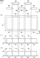
- FIG. 5A is a diagram showing the exposure fields PIa to PIe of the five projection optical systems 19a to 19e on the substrate 22.
- the exposure fields PIa and PIe of the projection optical systems 19a and 19e, which are the projection optical system 19F in the first row, are the short sides of the two sides parallel to the Y direction, like the exposure fields PIc of the projection optical system 19c described above. Is a trapezoid with the +X side and the long side on the -X side.
- the exposure field PId of the projection optical system 19d which is the second row of the projection optical system 19R, has the short side of the two sides parallel to the Y direction, which is the same as the exposure field PIb of the projection optical system 19b described above. It is a trapezoid with the long side on the +X side on the X side.
- the exposure fields PIa, PId, PIe of the projection optical systems 19a, 19d, 19e, the center areas PIac, PIdc, PIec, and the left end areas PIal, PIdl, PIel, and the right end area PIar are the same as the above-described exposure fields PIb, PIc. , PIdr, PIer can be defined.
- the exposure field PIa arranged at the end in the ⁇ Y direction blocks the illumination light by the field stop 21a so that the end in the ⁇ Y direction is parallel to the X direction, and thus the right end region PIar does not exist. ..
- the exposure visual field PIe arranged at the end in the +Y direction blocks the illumination light so that the end portion in the +Y direction is parallel to the X direction by the field diaphragm 21a, and thus the left end region PIal does not exist.
- the shapes of the field stops 21a and 21e may be different from the shape of the field stop 21c, or another member may be used to block the illumination light so that the right end area PIar does not exist in the exposure field PIa. You may do so.
- the lengths in the Y direction of the central regions PIac to PIec of the exposure fields PIa to PIe are all equal to the width Ws, and the lengths of the left end regions PIal to PIdl and the right end regions PIbr to PIer are equal to the width Wo.
- the positions of the left end regions PIal to PIdl and the right end regions PIbr to PIer adjacent to each other in the Y direction are the same.
- the shapes and positions of the exposure fields PIa to PIe are set by setting the positions of the projection optical systems 19a to 19e and the shapes and positions of the openings 21ao to 21eo of the field diaphragms 21a to 21e.
- FIG. 5B shows an exposure area formed on the substrate 22 when the substrate 22 is scanned in the X direction by the substrate stage and exposed by the exposure fields PIa to PIe shown in FIG. 5A. It is a figure.
- scanning exposure fields SIa to SIe are formed by scanning exposure fields PIa to PIe.
- the scanning exposure fields SIa, SIc, and SIe formed by the projection optical systems 19a, 19c, and 19e in the first row are indicated by chain double-dashed lines, and are formed by the projection optical systems 19b and 19d in the second row.
- the scanning exposure visual fields SIb and SId are indicated by a chain line.
- These scanning exposure fields SIa to SIe are the fields of view PIa to PIe extended in the X direction by scanning exposure in the X direction.
- the exposure area of the left end area PIal and the exposure area of the right end area PIbr match. The same applies to the other exposure areas, and thus the description thereof will be omitted.
- FIG. 5C is a graph showing an integrated exposure amount E exposed on the substrate 22 by scanning exposure in the X direction.
- the vertical axis of the graph is the integrated exposure amount
- the horizontal axis is the coordinate in the Y direction.
- the integrated values of the exposure fields PIa to PIe in the X direction are equal in each of the minute sections in the Y direction, and due to the action of the fly-eye lens 11 and the like, the exposure fields PIa to PIe within Since the illuminance is uniform, the integrated exposure amount E on the substrate 22 has a constant value E1.
- the integrated exposure dose E in the portions (hereinafter, also referred to as “non-overlap portions”) Sa to Se exposed by one of the scanning exposure visual fields SIa to SIe and the scanning exposure visual fields SIa to The integrated exposure dose E becomes equal to the integrated exposure dose E of the portions Oa to Od where the two Sie are overlapped and exposed (hereinafter, also referred to as “overlap portion”).
- an effective exposure amount (hereinafter, also referred to as “effective exposure amount”) is proportional to an integrated exposure amount. That is, as long as the integrated exposure amount is the same, the effective exposure of the photosensitive material can be achieved regardless of whether the exposure is performed continuously in time or divided into a plurality of portions in time. The amount does not change. Therefore, the effective exposure amount to the photosensitive material also becomes a constant value.
- the effective exposure of the photosensitive material is the same even if the cumulative exposure amount is the same.
- the photosensitivity changes. Specifically, when the exposure is divided into a plurality of pieces in terms of time, the effective exposure amount is lower than that in the case where the exposure is consecutively formed in terms of time.
- FIG. 5D shows an exposure field PIa to PIe shown in FIG. 5A in the X direction for such a part of the photosensitive material (hereinafter, also referred to as “non-additive photosensitive material”).
- 7 is a graph showing an effective exposure amount EE of a non-additive photosensitive material when scanning exposure is performed on the image.
- Overlapping portions Oa to Od where two scanning exposure fields SIa to SIe are overlapped and exposed are first exposed by the projection optical systems 19a, 19c and 19e in the first row, and then the projection optics in the second row. Since the exposure is performed by the systems 19b and 19d, the exposure is divided in time. In other words, the overlapping portions Oa to Od are exposed discretely in time.
- the effective exposure amount EE of the non-overlap portions Sa to Se exposed without being divided in time by one of the scanning exposure visual fields SIa to SIE is different from the effective exposure amount EE of the overlap portions Oa to Od. Is falling.
- the value of the effective exposure amount EE of the non-overlapping portions Sa to Se is EE1
- the value of the effective exposure amount EE of the overlapping portions Oa to Od is smaller than EE1.
- the effective exposure amount EE is different between the overlapping portions Oa to Od and the non-overlapping portions Sa to Se.
- the line width and thickness of the formed pattern will change.
- the positions on the incident surface side of the fly-eye lenses 11a to 11e of the illumination optical systems ILa to ILe that is, the positions between the input lenses 8a to 8e and the fly-eye lenses 11a to 11e.
- the light blocking members 10a to 10e are provided near the entrance surfaces of the fly-eye lenses 11a to 11e.
- the light blocking members 10a to 10e are movably held by the light blocking member holding portions 9a to 9e in the X direction, which is a direction substantially orthogonal to the optical axes Ixa to Ixe of the respective illumination optical systems ILa to ILe.
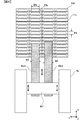
- FIG. 6 is a view of the fly-eye lens 11c, the light blocking member 10c, and the light blocking member holding portion 9c provided in the illumination optical system ILc as viewed from the input lens 8c side.
- the light blocking member 10c and the light blocking member holding portion 9c provided in the illumination optical system ILc will be described with reference to FIG. 6, but the light blocking members 10a to 10e provided in the other illumination optical systems ILa to ILe will be described. The same applies to 10e and the light shielding member holding portions 9a to 9e.
- each lens element 110 is a conjugate surface with respect to the exposure visual field PIc formed on the substrate 22, an area corresponding to the exposure visual field PIc in each lens element 110 (exposure visual field corresponding area) is shown in FIG. ) IPIc is indicated by a broken line.
- the width in the Y direction of the portion of the exposure visual field corresponding region IPIc corresponding to the central region PIcc of the exposure visual field PIc is the width IWs.
- the two light blocking members 10c1 and 10c2 forming the light blocking member 10c are the +Z of one or more lens elements 110 arranged on the ⁇ X direction side of two of the above lens blocks. It is located near the side.
- the widths W1 and W2 of the light shielding members 10c1 and 10c2 in the Y direction are substantially equal to the above-mentioned width IWs.
- the light blocking members 10c1 and 10c2 are held by a slider 9c1 which is a part of the light blocking member holding portion 9c, and the slider 9c1 is movable in the X direction with respect to the main body of the light blocking member holding portion 9c by a control system (not shown). ing.
- the relative positional relationship between the slider 9c1 and the main body of the light shielding member holding portion 9c is measured by an encoder or the like.
- the widths W1 and W2 of the light blocking members 10c1 and 10c2 in the Y direction are substantially equal to the above-described width IWs, the light blocking members 10c1 and 10c2 are exposed from some of the lens elements 110 to the exposure field PIc on the substrate 22. It is possible to block the light radiated to the central region PIcc. Further, by controlling the slider 9c1, it is possible to change the number of the lens elements 110 shielded by the light shielding members 10c1 and 10c2 and the ratio of the shielded portions within one lens element 110. As a result, the illuminance of the central region PIcc of the exposure visual field PIc can be variably and continuously reduced with respect to the illuminance of the left end region PIcl and the right end region PIcr.
- the light shielding member 10c can be interpreted as an illuminance changing member that reduces the integrated exposure amount to the non-overlap portion on the substrate 22 with respect to the integrated exposure amount to the overlap portion.
- the light blocking member 10c may be a thin metal plate or a light blocking film formed by a light blocking member on a transparent glass plate.
- the light blocking member 10c is not limited to a member that completely blocks the illumination light such as a filter, and may be a member that blocks and transmits only a part of the illumination light. That is, the light blocking member 10c may be any illuminance changing member for changing the illuminance.
- the light blocking members 10a to 10e and the light blocking member holding portions 9a to 9e included in the other illumination optical systems ILa to ILe have the same structures as the above-described light blocking member 10c and the light blocking member holding portion 9c.
- FIG. 7 is a diagram for explaining the result when the pattern is exposed and transferred using the non-additive photosensitive material in the exposure apparatus 100 of the first embodiment including the light shielding members 10a to 10e. Similar to FIG. 5A, FIG. 7A shows each exposure visual field PIa to PIe on the substrate 22. Similar to FIG. 5C, FIG. 7B is a graph showing an integrated exposure amount E exposed on the substrate 22 by scanning exposure in the X direction. In the case shown in FIG. 7B, the light blocking members 10a to 10e are inserted into the entrance surfaces of the fly-eye lenses 11a to 11e by the light blocking member holding portions 9a to 9e.
- the integrated exposure amount E2 of the non-overlap portions Sa to Se exposed by one of the scanning exposure visual fields SIa to SIE is equal to the overlapping portion exposed by overlapping two scanning exposure visual fields SIa to SIE. It is smaller than the integrated exposure amount E3 of Oa to Od.
- FIG. 7C is a graph showing the effective exposure amount EE generated in the non-additive photosensitive material by the integrated exposure amount shown in FIG. 7B.
- the edges in the XY directions of the light blocking member 10c are blurred on the incident surface of the fly-eye lens 11c. Projected.
- how much the light blocking member 10c should be arranged in the Z direction from the incident surface of the fly-eye lens 11c is a parameter that determines the amount of penumbra blur on the edge of the light blocking member 10c on the substrate 22. That is, it can be determined based on the lateral magnification between the incident surface of the fly-eye lens 11c and the substrate 22 and the numerical aperture of the illumination light on the incident surface of the fly-eye lens 11c.
- the widths of the overlapping portions Oa to Od on the substrate 22 in the Y direction can also be taken into consideration and determined.
- the light blocking member holding portions 9a to 9e can change the positions of the light blocking members 10a to 10e in the Z direction with respect to the incident surfaces of the fly eye lenses 11a to 11e, that is, the light blocking members 10a to 10e and the fly eye lenses 11a to 11e in the Z direction. You may have the structure which can change the distance with 11e.
- the widths of the overlapping portions Oa to Od in the Y direction are DW
- the lateral magnification of the substrate 22 with respect to the incident surface of the fly-eye lens 11c is ⁇
- the numerical aperture of illumination light on the incident surface of the fly-eye lens 11c is NA.
- the distance D in the Z direction from the incident surface of the fly-eye lens 11c of the light blocking member 10c is 0 ⁇ D ⁇ 1.2 x DW/( ⁇ NA) (1) It is good to When the distance D satisfies the formula (1), the influence of the exposure amount change (exposure amount unevenness) on the substrate 22 due to the edge of the light shielding member 10c can be further reduced, and the integrated exposure of the overlapping portions Oa to Od can be performed. It is possible to prevent the amount from decreasing more than necessary.
- the relationship between the effective exposure amount of the non-additive photosensitive material and the integrated exposure amount for time-divided exposure differs depending on each non-additive photosensitive material. Therefore, before actual exposure is performed on a specific non-additive photosensitive material, for example, test exposure is performed under a plurality of conditions in which the insertion amount (position in the X direction) of the light shielding member 10c is set to different stages, that is, light shielding is performed. It is advisable to change the number of lens elements 110 that are shielded by the member 10c, perform test exposure, and determine the optimum insertion amount from the results. Further, when determining the insertion amount of the light shielding member 10c, it is preferable to use the illuminance sensor 26 provided on the substrate stage 27 while measuring the illuminance of the central region PIcc in the exposure field PIc.
- each lens element 110 has the exposure visual field corresponding region IPIc corresponding to the exposure visual field PIc, but the exposure visual field corresponding region IPIc spreads over the entire surface of the lens element 110 in the X direction. is not. That is, both ends of the lens element 110 in the X direction are portions that do not correspond to the exposure visual field PIc on the substrate 22 and are projected onto the visual field stop 21c in the projection optical system 19c and shielded by the visual field stop 21c. ..
- the ends of the two light blocking members 10c1 and 10c2 in the +X direction are displaced by half the pitch PX of the arrangement of the lens elements 110 in the X direction.
- the other +X direction end of one of the two light blocking members 10c1 and 10c2 is a lens. It is arranged near the center of the element 110 in the X direction. Therefore, the integrated exposure amount on the substrate 22 can be constantly changed by moving the two light blocking members 10c1 and 10c2 together in the X direction.
- the two light blocking members 10c1 and 10c2 may have the same length in the X direction. In this case, it is preferable that the light shielding members 10c1 and 10c2 be independently movable in the X direction. As a result, the light blocking amount can be different for each lens element 110.
- the light blocking members 10c1 and 10c2 are not limited to the above two, but may be three or more, and each may be arranged in a different lens block. Also in this case, if the number of light-shielding members is m (m is a natural number of 2 or more), the end portions in the +X direction of each light-shielding member are set to be shifted by PX/m with respect to the pitch PX. Is preferred.
- the light blocking member 10c is arranged at a position separated from the incident surface of the fly-eye lens 11c in the Z direction by a predetermined distance, the invention is not limited to this.
- the light blocking member 10c may be provided at a position that is an incident surface of the fly-eye lens 11c, that is, a conjugate surface of the substrate.
- the light-shielding member 10c has a shape (width) in the Y direction that changes depending on the position in the X direction, or a filter whose transmittance changes depending on the location, such as illumination light depending on the position in the Y direction. It is preferable that the shading rate of No. 2 continuously changes. If the light blocking member 10c completely blocks the illumination light, the ratio of the cumulative exposure amount of the overlapping portions Oa to Od to the cumulative exposure amount of the non-overlapping portions Sa to Se changes discontinuously. There is a risk that it will happen and you can prevent it.
- the number of projection optical systems 19a to 19e is not limited to five, and any number such as three or eight may be used.
- the plurality of projection optical systems 19a to 19e are provided, and the plurality of exposure visual fields SIa to SIe formed by the respective projection optical systems are mutually made by one scanning in the X direction. It is said that they overlap in the Y direction.
- there is only one projection optical system and scanning exposure of the substrate 22 in the X direction is performed a plurality of times while moving the substrate 22 and the mask 15 in the Y direction, and a plurality of exposure fields formed by each scanning exposure are obtained. They may overlap each other in the Y direction.
- the illumination optical system corresponding to one projection optical system has the same configuration as the above-mentioned illumination optical systems ILa to ILe.
- An apparatus having a plurality of projection optical systems 19a to 19e as in the first embodiment described above can expose a larger area on the substrate 22 by one scanning exposure, and has excellent processing capability. There is.
- the plurality of projection optical systems 19a to 19e are assumed to be total refraction optical systems, but the present invention is not limited to this, and catadioptric optical systems or total reflection optical systems can be adopted.
- the shape of the exposure visual fields PIa to PIe is a trapezoid, but this is not limited to a trapezoid, and, for example, the shape of the portion corresponding to the central portion is
- the field of view may be a circular arc and includes a right end region and a left end region of a triangle at both ends of the arc.
- the optical axes PXa to PXe of the projection optical systems 19a to 19e and the optical axes IXa to IXe of the illumination optical systems ILa to ILe are basically set parallel to the Z direction. I am supposed to. However, when a bending mirror is used in any of the optical systems, the optical axis direction is not parallel to the Z direction. Further, when a bending mirror is used in any of the optical systems, the moving direction of the light blocking members 10a to 10e is also different from the scanning direction (X direction) of the substrate 22.
- the light blocking members 10a to 10e move in a direction optically corresponding to the scanning direction of the substrate 22 based on the conjugate relationship between the substrate 22 including the folding mirror and the fly-eye lenses 11a to 11e. It should be free.
- each of the projection optical systems 19a to 19e is provided with two optical systems, that is, the first optical system 19F and the second optical system 19R in the X direction.
- this is not limited to two rows, and three or more rows of optical systems may be arranged in the X direction.
- a rod integrator can be used instead of the fly-eye lens 11 described above.
- the conjugate surface with the substrate 22 and the mask 15 is on the emitting side of the rod integrator (the side of the mask 15), and therefore the light shielding member 10 is also arranged near the emitting side of the rod integrator. Then, the vicinity of one end on the X side of the exit surface of the rod integrator is partially shielded from light.
- the light shielding members 10a to 10e may be arranged near the intermediate image plane 20 of the projection optical systems 19a to 19e.
- the light blocking member is configured to block light in the vicinity of the intermediate image plane 20 in the portions corresponding to the central regions PIac to PIec of the exposure fields PIa to PIe.
- an intermediate image plane (a conjugate plane to the mask 15) is provided inside the illumination optical systems ILa to ILe, and an intermediate image plane in the illumination optical systems ILa to ILe is provided.
- a field diaphragm may be provided on the image plane to define the shapes of the exposure fields PIa to PIe on the substrate 22.
- the projection optical systems 19a to 19e and the illumination optical systems ILa to ILe are fixed, and the substrate 22 is moved by the substrate stage 27. Instead, the projection optical systems 19a to 19e and the illumination optical systems are used.
- the systems ILa to ILe may be provided on the scanning stage to scan the substrate 22.
- the mask 15 is not limited to a mask having a pattern formed on a glass substrate, but may be a variable shaping mask including a digital multi-mirror device or a liquid crystal device.
- the exposure apparatus of the first embodiment or the modified example includes projection optical systems 19a to 19e, illumination optical systems ILa to ILe that supply illumination light to the projection optical systems 19a to 19e, a substrate 22 to be exposed, and projection optics.
- a scanning stage (substrate stage) 27 that relatively scans the systems 19a to 19e in the scanning direction, and the plurality of scanning exposure fields SIa to SIe by the projection optical systems 19a to 19e are overlapped in the non-scanning direction.
- the illumination optical systems ILa to ILe or the projection optical systems 19a to 19e cause the integrated exposure of the non-overlapping portions Sa to Se which are exposed on the substrate 22 to be exposed without overlapping during exposure.
- the illuminance changing members 10a to 10e are set so that the amount thereof becomes smaller than the integrated exposure amount of the overlapping portions Oa to Od which are overlapped and exposed on the exposed substrate 22. With this configuration, when the exposure is divided into a plurality of pieces in terms of time, the effective exposure amount is lower than that in the case of consecutive exposure. Even when transfer is performed, the line width of the transferred pattern between the overlapping portions Oa to Od where the scanning exposure fields SIa to SIe overlap and the non-overlapping portions Sa to Se. It is possible to prevent changes in thickness and thickness.
- the illumination optical systems ILa to ILe include optical integrators 11a to 11e, and the illuminance changing members 10a to 10e are in the vicinity of the conjugate surface of the exposed substrate 22 of the optical integrators 11a to 11e and overlap the portion Oa to.
- Shielding members 10a to 10e provided at positions distant from each other in the IXa to IXe directions.
- the shielding members 10a to 10e are arranged in a scanning direction substantially orthogonal to the optical axes IXa to IXe of the illumination optical systems ILa to ILe. It has light-shielding member holding portions 9a to 9e, which are held so as to be movable in the optically corresponding first direction. With this configuration, by moving the light shielding members 10a to 10e in the first direction, the ratio of the integrated exposure amount of the overlapping portions Oa to Od to the integrated exposure amount of the non-overlap portions Sa to Se is made substantially continuous. Can be lowered while changing to.
- 100 exposure device, 1: light source, ILa to ILe: illumination optical system, 10a to 10e: light blocking member (illuminance changing member), 11a to 11e: fly-eye lens, 12a to 12e: condenser lens, 15: mask, MIa to MIe: illumination field, 19a to 19e: projection optical system, 21a to 21e: field diaphragm, 22: substrate, SIa to SIe: scanning exposure field, Sa to Se: non-overlap area, Oa to Od: overlap area
Landscapes
- Physics & Mathematics (AREA)
- General Physics & Mathematics (AREA)
- Exposure And Positioning Against Photoresist Photosensitive Materials (AREA)
Abstract
Description
さらに、複数の投影光学系を非スキャン方向に並列的に備え、複数の投影光学系が露光する露光視野の一部をオーバーラップさせつつ露光を行うことで、一回の走査により基板上に電子回路を露光転写する方法も知られている(例えば特許文献1)。
図1は、第1実施形態の露光装置100を示す側面図である。後述するように露光装置100は、5本の投影光学系19a~19eを備えているが、図1には、そのうちの2本である投影光学系19a、19bのみが示されている。
投影光学系19a~19eは、投影倍率(横倍率)が+1倍の正立正像を形成する光学系であり、マスク15に描画されているパターンを、基板22の上面に形成されている感光材料に露光転写する。
位置検出光学系23は、基板22上に形成されているアライメントマーク等の既存のパターンの位置を検出する。
本明細書では、露光に際して、基板22が走査される方向(X方向)を「走査方向」および「スキャン方向」とも呼ぶ。また、基板22の面内に含まれる方向であってX方向と直交する方向(Y方向)を「非走査方向」および「非スキャン方向」とも呼ぶ。Z方向は、X方向およびY方向と直交する方向である。
なお、図1および以下の各図に矢印で示したX方向、Y方向、およびZ方向は、その矢印の指し示す方向を+方向とする。
図2に示したとおり、5つの投影光学系19a~19eのうち、3つの投影光学系19a、19c、19e(以下、総称してまたは個々に「第1列の投影光学系19F」とも呼ぶ)は、Y方向に並んで配置されている。そして、2つの投影光学系19b、19d(以下、総称してまたは個々に「第2列の投影光学系19R」とも呼ぶ)は、Y方向に並んで、第1列の投影光学系19Fよりも+X側に配置されている。
第1列の投影光学系19Fの各投影光学系は、その光軸がY方向に所定の間隔で離れて配置される。第2列の投影光学系19Rの各光学系も第1列の投影光学系19Fと同様に配置される。また、投影光学系19bは、その光軸のY方向の位置が、投影光学系19aと投影光学系19cのそれぞれの光軸を結んだ直線の略中心と一致するように、配置される。また、投影光学系19dも、投影光学系19bと同様に、配置される。
なお、側面図である図1には、投影光学系19c~19eは、投影光学系19aまたは19bとX方向の位置が重なるため示していない。同様に、照明光学系ILc~ILeも、照明光学系ILaまたはILbとX方向の位置が重なるため示していない。
フライアイレンズ11cは、照明領域MIcと相似形の、Y方向に長い長方形の断面形状(XY面内の形状)を有するレンズエレメント110が、X方向およびY方向に複数個配列されて形成されている。各レンズエレメント110の入射面(図3中の上方の面、すなわち+Z側の面)は、各レンズエレメント110およびコンデンサーレンズ12cからなる光学系により、マスク15上の照明領域MIcに対する共役面となっている。従って、基板22上の露光視野PIcに対する共役面でもある。それぞれのレンズエレメント110の入射面に照射される照明光は、マスク15上の照明領域MIcに重畳して照射される。これにより、照明領域MIc内の照明光の照度が略均一化される。
フライアイレンズ11a~11eは、それぞれの照明領域MIa~照明領域MIeに照明光を重畳して照射するオプチカルインテグレーターの一例である。
図4(a1)は、投影光学系19cに対応するマスク15上の照明領域MIcを示す図であり、照明領域MIcは、フライアイレンズ11cのレンズエレメント110の断面形状と相似な長方形となっている。
一例として、投影光学系19c~19eが全屈折光学系から成るとき、中間像である照明光MIC2は照明領域MIcに対する倒立正像(像のX方向およびY方向が共に反転し、鏡像ではない像)であり、露光視野PIcは視野絞り21cに対する倒立正像となる。従って、図4(a2)および図4(a3)に示したとおり、視野絞り21cの開口部21coの形状と、露光視野PIcの形状は、相互にZ軸回りに180度回転したものと一致する。
中心領域PIccのY方向の長さ(幅)を幅Wsと呼び、左端領域PIclおよび右端領域PIcrのY方向の長さ(幅)は等しく、これを幅Woと呼ぶ。
各露光視野PIa~PIeのこのような形状および位置の設定は、投影光学系19a~19eの配置位置、および視野絞り21a~21eの開口部21ao~21eoの形状および位置を設定することにより行なう。
すなわち、Y方向のうち、各走査露光視野SIa~SIeの1つにより露光された部分(以下、「非オーバーラップ部」とも呼ぶ)Sa~Seにおける積算露光量Eと、各走査露光視野SIa~SIeの2つがオーバーラップして露光された部分(以下、「オーバーラップ部」とも呼ぶ)Oa~Odにおける積算露光量Eとは、共に積算露光量Eの値がE1となり等しくなる。
従って、感光材料への実効感光量も一定値となる。
各走査露光視野SIa~SIeの2つがオーバーラップして露光されたオーバーラップ部Oa~Odは、始めに第1列の投影光学系19a、19c、19eにより露光され、その後第2列の投影光学系19b、19dにより露光されるため、露光が時間的に分割されて行われている。換言すると、オーバーラップ部Oa~Odは、時間的に離散的に露光が行われる。従って、各走査露光視野SIa~SIeの1つにより時間的に分割されずに露光された非オーバーラップ部Sa~Seの実効感光量EEに対して、オーバーラップ部Oa~Odの実効感光量EEが低下している。具体的には、非オーバーラップ部Sa~Seの実効感光量EEの値がEE1に対して、オーバーラップ部Oa~Odの実効感光量EEの値はEE1よりも小さくなる。
遮光部材保持部9cが遮光部材10c1、10c2をX方向に移動させることにより、遮光部材10c1、10c2により一部のレンズエレメント110を遮光することができる。先述のとおり、遮光部材10c1、10c2のY方向の幅W1、W2は、上述の幅IWsと略等しいことから、遮光部材10c1、10c2は、一部のレンズエレメント110から基板22上の露光視野PIcのうちの中心領域PIccに照射される光を遮光することができる。さらに、スライダー9c1を制御することにより、遮光部材10c1、10c2により遮光されるレンズエレメント110の数、および1つのレンズエレメント110内の遮光された部分の比率を変更することができる。これにより、露光視野PIcのうち中心領域PIccの照度を、左端領域PIclおよび右端領域PIcrの照度に対して、略連続して可変に低下させることができる。
遮光部材10cは、金属製の薄板であっても良く、透明なガラス板上に遮光部材により形成された遮光膜であってもよい。遮光部材10cは、フィルタのように照明光を完全に遮光するものに限られず、一部の照明光のみを遮光、透過させる部材であっても良い。つまり遮光部材10cは、照度を変更するための照度変更部材であればよい。
他の照明光学系ILa~ILeが備える遮光部材10a~10e、および遮光部材保持部9a~9eについても、上述の遮光部材10cおよび遮光部材保持部9cの構造と、同様である。
図7(b)に示した場合においては、遮光部材保持部9a~9eにより遮光部材10a~10eがフライアイレンズ11a~11eの入射面内に挿入されている。従って、各走査露光視野SIa~SIeの1つにより露光された非オーバーラップ部Sa~Seの積算露光量E2は、各走査露光視野SIa~SIeの2つがオーバーラップして露光されたオーバーラップ部Oa~Odの積算露光量E3と比較して少ない。
これにより、非加算性感光材料を使用してパターンの露光転写を行った場合であっても、各走査露光視野SIa~SIeがオーバーラップするオーバーラップ部Oa~Odと、非オーバーラップ部Sa~Se部との間での、転写されたパターンの線幅や厚さの変化を防止することができる。
0 ≦ D ≦ 1.2×DW/(β・NA) ・・・(1)
とするのが良い。
距離Dが式(1)を満たす場合、遮光部材10cのエッジによる基板22上の露光量変化(露光量ムラ)の影響をさらに低減することができ、かつ、オーバーラップ部Oa~Odの積算露光量が必要以上に低下することを防止できる。
また、遮光部材10cの挿入量の決定に際しては、基板ステージ27上に設けた照度センサ26を使用して、露光視野PIc内の中心領域PIccの照度を計測しながら行うと良い。
そこで、第1実施形態においては、2本の遮光部材10c1、10c2のそれぞれの+X方向の端部を、レンズエレメント110のX方向の配列のピッチPXの半分だけずらしている。
以上の第1の実施形態においては、5つの投影光学系19a~19eを有するものとしたが、投影光学系の本数は5つに限られるわけではなく、3つや8つなど、いくつであってもよい。
また、以上の第1の実施形態においては、複数の投影光学系19a~19eを有し、1度のX方向の走査により、各投影光学系が形成する複数の露光視野SIa~SIeが相互にY方向にオーバーラップするとしている。
しかし、投影光学系は1つであり、基板22のX方向への走査露光を、基板22およびマスク15をY方向に移動させつつ複数回行い、各走査露光により形成される複数の露光視野を相互にY方向にオーバーラップさせてもよい。この場合にも、1つの投影光学系に対応する照明光学系は、上述の照明光学系ILa~ILeと同様の構成を備えることが望ましい。
なお、上述の第1実施形態のように複数の投影光学系19a~19eを有する装置は、一度の走査露光で基板22上の、より多くの面積を露光することができ、処理能力に優れている。
また、以上の第1の実施形態においては、露光視野PIa~PIeの形状は台形であるとしたが、これは台形に限られるものではなく、例えば、その上記中心部分に相当する部分の形状が円弧であり、円弧の両端に三角形の右端領域および左端領域を備える視野であってもよい。
また、いずれかの光学系の中に折り曲げミラーが採用されている場合には、遮光部材10a~10eの移動方向も基板22の走査方向(X方向)とは異なる方向になる。しかし、この場合であっても、遮光部材10a~10eは、折り曲げミラーを含めた基板22とフライアイレンズ11a~11eの共役関係に基づいて基板22の走査方向に光学的に対応する方向に移動自在とすれば良い。
また、マスク15は、ガラス基板上にパターンが形成されたマスクに限らず、デジタルマルチミラーデバイスや液晶デバイスからなる可変整形マスクであってもよい。
(1)第1実施形態または変形例の露光装置は、投影光学系19a~19eと、投影光学系19a~19eに照明光を供給する照明光学系ILa~ILeと、被露光基板22と投影光学系19a~19eとを走査方向に相対走査する走査ステージ(基板ステージ)27と、を備え、投影光学系19a~19eによる走査露光視野SIa~SIeを、非走査方向に複数個オーバーラップさせて前記被露光基板22を露光するとともに、照明光学系ILa~ILeまたは投影光学系19a~19eは、露光において、被露光基板22上でオーバーラップなしで露光される非オーバーラップ部Sa~Seの積算露光量が、被露光基板22上でオーバーラップされて露光されるオーバーラップ部Oa~Odの積算露光量に比べて小さくなるように設定する照度変更部材10a~10eを有している。
この構成により、露光が時間的に複数に分割して行われた場合に時間的に連続して行われた場合に比べて実効感光量が低下する非加算性感光材料を使用してパターンの露光転写を行った場合であっても、各走査露光視野SIa~SIeがオーバーラップするオーバーラップ部Oa~Odと、非オーバーラップ部Sa~Se部との間での、転写されたパターンの線幅や厚さの変化を防止することができる。
この構成により、遮光部材10a~10eを第1方向に移動させることにより、オーバーラップ部Oa~Odの積算露光量の、非オーバーラップ部Sa~Se部の積算露光量に対する比率を、ほぼ連続的に変化させつつ低下させることができる。
日本国特願2019-002235号(2019年1月9日出願)
Claims (10)
- 投影光学系と、
前記投影光学系に照明光を供給する照明光学系と、
被露光基板と前記投影光学系とを走査方向に相対走査する走査ステージと、
を備え、
前記走査ステージは、前記投影光学系による走査露光視野を複数個オーバーラップさせて前記被露光基板を露光するよう、前記被露光基板を前記投影光学系に対して相対走査させ、
前記照明光学系または前記投影光学系は、前記露光において、前記被露光基板上でオーバーラップなしで露光される非オーバーラップ部の露光量が、前記被露光基板上でオーバーラップされて露光されるオーバーラップ部の露光量に比べて小さくなるように設定する照度変更部材を有する、露光装置。 - 請求項1に記載の露光装置において、
前記照明光学系は、オプチカルインテグレーターを有し、
前記照度変更部材は、前記オプチカルインテグレーターの前記被露光基板の共役面の近傍に設けられ、
前記照度変更部材を、前記照明光学系の光軸と略直交する方向であって前記走査方向に光学的に対応する第1方向に移動させ露光量を制御可能に設けられる露光装置。 - 請求項2に記載の露光装置であって、
前記照度変更部材は、前記オーバーラップ部の前記走査方向と直交する非走査方向の幅、前記共役面と前記被露光基板との横倍率、および前記共役面における照明光の開口数に応じて定まる所定距離だけ、前記共役面から前記照明光学系の光軸方向に離れた位置に設けられる、露光装置。 - 請求項1に記載の露光装置において、
前記照明光学系は、フライアイレンズを有し、
前記照度変更部材は、前記被露光基板の共役面である前記フライアイレンズの入射側面または前記入射側面より光源側にある前記入射側面と共役な面の位置、またはその位置から所定距離だけ離れた位置に設けられている、露光装置。 - 請求項4に記載の露光装置において、
前記照度変更部材を、前記照明光学系の光軸と略直交する方向であって前記走査方向に光学的に対応する第1方向に移動させ露光量を制御可能に設けられる、露光装置。 - 請求項5に記載の露光装置であって、
前記照度変更部材は、前記オーバーラップ部の前記と直交する非走査方向の幅、前記共役面と前記被露光基板との横倍率、および前記共役面における照明光の開口数に応じて定まる所定距離だけ、前記共役面から前記照明光学系の光軸方向に離れた位置に設けられる、露光装置。 - 請求項6に記載の露光装置において、
前記フライアイレンズは、前記第1方向に配列されている複数のレンズエレメントを含むレンズブロックが、前記照明光学系の光軸および前記第1方向と直交する第2方向に複数配列されているとともに、
前記照度変更部材は、少なくとも1つの前記レンズブロックの中の前記第1方向の一方の側に配置されている1つ以上のレンズエレメントの、前記非オーバーラップ部と共役な部分の少なくとも一部を遮光する、露光装置。 - 請求項7に記載の露光装置において、
前記照度変更部材は、複数の前記レンズブロックのうちのm個(mは2以上の自然数)のレンズブロックのそれぞれに対応して、m個配置される、露光装置。 - 請求項8に記載の露光装置において、
前記m個の前記照度変更部材の前記第1方向の前記一方の側と反対側の他方の側の端部は、前記レンズブロック内の前記レンズエレメントの前記第1方向の配列の周期をPとして、前記第1方向にそれぞれP/mだけ異なる位置に設定されている、露光装置。 - 請求項1から請求項9までのいずれか一項に記載の露光装置において、
前記投影光学系および照明光学系を複数並列して備え、
一度の前記相対走査により複数の前記走査露光視野を非走査方向に複数個オーバーラップさせて前記被露光基板を露光する、露光装置。
Priority Applications (4)
| Application Number | Priority Date | Filing Date | Title |
|---|---|---|---|
| KR1020217023788A KR102856496B1 (ko) | 2019-01-09 | 2019-12-16 | 노광 장치 |
| JP2020565656A JPWO2020145044A1 (ja) | 2019-01-09 | 2019-12-16 | 露光装置 |
| CN201980088088.8A CN113272737B (zh) | 2019-01-09 | 2019-12-16 | 曝光装置 |
| JP2024112353A JP7747132B2 (ja) | 2019-01-09 | 2024-07-12 | 露光装置 |
Applications Claiming Priority (2)
| Application Number | Priority Date | Filing Date | Title |
|---|---|---|---|
| JP2019-002235 | 2019-01-09 | ||
| JP2019002235 | 2019-01-09 |
Publications (1)
| Publication Number | Publication Date |
|---|---|
| WO2020145044A1 true WO2020145044A1 (ja) | 2020-07-16 |
Family
ID=71521284
Family Applications (1)
| Application Number | Title | Priority Date | Filing Date |
|---|---|---|---|
| PCT/JP2019/049137 Ceased WO2020145044A1 (ja) | 2019-01-09 | 2019-12-16 | 露光装置 |
Country Status (5)
| Country | Link |
|---|---|
| JP (2) | JPWO2020145044A1 (ja) |
| KR (1) | KR102856496B1 (ja) |
| CN (1) | CN113272737B (ja) |
| TW (1) | TWI828831B (ja) |
| WO (1) | WO2020145044A1 (ja) |
Cited By (2)
| Publication number | Priority date | Publication date | Assignee | Title |
|---|---|---|---|---|
| KR20240017069A (ko) * | 2021-07-05 | 2024-02-06 | 가부시키가이샤 니콘 | 노광 장치, 노광 방법 및 플랫 패널 디스플레이의 제조 방법, 그리고 노광 데이터 작성 방법 |
| WO2026100397A1 (ja) * | 2024-11-07 | 2026-05-15 | 株式会社ニコン | 露光方法、露光装置、及びデバイス製造方法 |
Families Citing this family (1)
| Publication number | Priority date | Publication date | Assignee | Title |
|---|---|---|---|---|
| JP7600195B2 (ja) | 2022-09-22 | 2024-12-16 | キヤノン株式会社 | 決定方法、プログラム、情報処理装置、露光装置、および物品製造方法 |
Citations (5)
| Publication number | Priority date | Publication date | Assignee | Title |
|---|---|---|---|---|
| JP2001060546A (ja) * | 1999-08-20 | 2001-03-06 | Nikon Corp | 露光方法及び露光装置 |
| JP2001297975A (ja) * | 2000-04-17 | 2001-10-26 | Nikon Corp | 露光装置及び露光方法 |
| JP2002258489A (ja) * | 2000-04-20 | 2002-09-11 | Nikon Corp | 露光装置および露光方法 |
| JP2016024257A (ja) * | 2014-07-17 | 2016-02-08 | 株式会社ニコン | 露光方法及び装置、並びにデバイス製造方法 |
| JP2019028084A (ja) * | 2017-07-25 | 2019-02-21 | 凸版印刷株式会社 | 露光装置 |
Family Cites Families (11)
| Publication number | Priority date | Publication date | Assignee | Title |
|---|---|---|---|---|
| WO2000011706A1 (en) * | 1998-08-18 | 2000-03-02 | Nikon Corporation | Illuminator and projection exposure apparatus |
| TWI610342B (zh) * | 2003-09-29 | 2018-01-01 | 尼康股份有限公司 | 曝光裝置及曝光方法、以及元件製造方法 |
| AU2005272460B2 (en) * | 2004-08-12 | 2012-03-22 | Nikon Corporation | Substrate Processing System, Method Of Confirmation Of Its State Of Use, And Method Of Prevention Of Illicit Use |
| WO2007066700A1 (ja) * | 2005-12-09 | 2007-06-14 | Nikon Corporation | レーザ光源装置、並びに露光方法及び装置 |
| JP5326928B2 (ja) * | 2009-08-19 | 2013-10-30 | 株式会社ニコン | 照明光学系、露光装置、およびデバイス製造方法 |
| JP6089603B2 (ja) * | 2012-11-06 | 2017-03-08 | 岩崎電気株式会社 | 疑似太陽光照射装置 |
| JP2016054230A (ja) | 2014-09-04 | 2016-04-14 | キヤノン株式会社 | 投影露光装置及び露光方法 |
| KR102567319B1 (ko) * | 2016-04-28 | 2023-08-16 | 엘지디스플레이 주식회사 | 분할노광 장치 및 이를 이용한 액정표시장치의 제조방법 |
| KR20210144672A (ko) * | 2019-03-29 | 2021-11-30 | 가부시키가이샤 니콘 | 노광 장치, 조명 광학계 및 디바이스 제조 방법 |
| CN113439239B (zh) * | 2019-03-29 | 2024-03-26 | 株式会社尼康 | 曝光装置、照明光学系统以及元件制造方法 |
| KR20260014705A (ko) * | 2019-03-29 | 2026-01-30 | 가부시키가이샤 니콘 | 노광 장치, 조명 광학계, 및 디바이스 제조 방법 |
-
2019
- 2019-12-16 KR KR1020217023788A patent/KR102856496B1/ko active Active
- 2019-12-16 WO PCT/JP2019/049137 patent/WO2020145044A1/ja not_active Ceased
- 2019-12-16 CN CN201980088088.8A patent/CN113272737B/zh active Active
- 2019-12-16 JP JP2020565656A patent/JPWO2020145044A1/ja active Pending
- 2019-12-25 TW TW108147659A patent/TWI828831B/zh active
-
2024
- 2024-07-12 JP JP2024112353A patent/JP7747132B2/ja active Active
Patent Citations (5)
| Publication number | Priority date | Publication date | Assignee | Title |
|---|---|---|---|---|
| JP2001060546A (ja) * | 1999-08-20 | 2001-03-06 | Nikon Corp | 露光方法及び露光装置 |
| JP2001297975A (ja) * | 2000-04-17 | 2001-10-26 | Nikon Corp | 露光装置及び露光方法 |
| JP2002258489A (ja) * | 2000-04-20 | 2002-09-11 | Nikon Corp | 露光装置および露光方法 |
| JP2016024257A (ja) * | 2014-07-17 | 2016-02-08 | 株式会社ニコン | 露光方法及び装置、並びにデバイス製造方法 |
| JP2019028084A (ja) * | 2017-07-25 | 2019-02-21 | 凸版印刷株式会社 | 露光装置 |
Cited By (3)
| Publication number | Priority date | Publication date | Assignee | Title |
|---|---|---|---|---|
| KR20240017069A (ko) * | 2021-07-05 | 2024-02-06 | 가부시키가이샤 니콘 | 노광 장치, 노광 방법 및 플랫 패널 디스플레이의 제조 방법, 그리고 노광 데이터 작성 방법 |
| KR102953844B1 (ko) * | 2021-07-05 | 2026-04-16 | 가부시키가이샤 니콘 | 노광 장치, 노광 방법 및 플랫 패널 디스플레이의 제조 방법, 그리고 노광 데이터 작성 방법 |
| WO2026100397A1 (ja) * | 2024-11-07 | 2026-05-15 | 株式会社ニコン | 露光方法、露光装置、及びデバイス製造方法 |
Also Published As
| Publication number | Publication date |
|---|---|
| CN113272737B (zh) | 2024-03-15 |
| TW202032287A (zh) | 2020-09-01 |
| JP7747132B2 (ja) | 2025-10-01 |
| JP2024138485A (ja) | 2024-10-08 |
| TWI828831B (zh) | 2024-01-11 |
| CN113272737A (zh) | 2021-08-17 |
| KR20210111271A (ko) | 2021-09-10 |
| JPWO2020145044A1 (ja) | 2021-11-18 |
| KR102856496B1 (ko) | 2025-09-05 |
Similar Documents
| Publication | Publication Date | Title |
|---|---|---|
| JP7747132B2 (ja) | 露光装置 | |
| JP7582181B2 (ja) | 露光装置、照明光学系、およびデバイス製造方法 | |
| JP7663146B2 (ja) | 露光装置 | |
| KR101501303B1 (ko) | 조명 광학 장치, 노광 장치, 및 디바이스 제조 방법 | |
| KR101662882B1 (ko) | 노광 장치 및 물품의 제조 방법 | |
| TWI874373B (zh) | 曝光裝置、照明光學系統以及元件製造方法 | |
| JP2019028084A (ja) | 露光装置 | |
| JP2013021265A (ja) | 照明装置、露光装置、露光方法、およびデバイス製造方法 | |
| KR20250141777A (ko) | 필터 유닛, 조명 유닛, 노광 장치, 및 노광 방법 | |
| JP2000321784A (ja) | 露光方法および露光装置 |
Legal Events
| Date | Code | Title | Description |
|---|---|---|---|
| 121 | Ep: the epo has been informed by wipo that ep was designated in this application |
Ref document number: 19908734 Country of ref document: EP Kind code of ref document: A1 |
|
| ENP | Entry into the national phase |
Ref document number: 2020565656 Country of ref document: JP Kind code of ref document: A |
|
| NENP | Non-entry into the national phase |
Ref country code: DE |
|
| ENP | Entry into the national phase |
Ref document number: 20217023788 Country of ref document: KR Kind code of ref document: A |
|
| 122 | Ep: pct application non-entry in european phase |
Ref document number: 19908734 Country of ref document: EP Kind code of ref document: A1 |