WO2020145032A1 - 物理量測定装置 - Google Patents
物理量測定装置 Download PDFInfo
- Publication number
- WO2020145032A1 WO2020145032A1 PCT/JP2019/048882 JP2019048882W WO2020145032A1 WO 2020145032 A1 WO2020145032 A1 WO 2020145032A1 JP 2019048882 W JP2019048882 W JP 2019048882W WO 2020145032 A1 WO2020145032 A1 WO 2020145032A1
- Authority
- WO
- WIPO (PCT)
- Prior art keywords
- circuit board
- printed circuit
- physical quantity
- silicone adhesive
- measuring device
- Prior art date
- Legal status (The legal status is an assumption and is not a legal conclusion. Google has not performed a legal analysis and makes no representation as to the accuracy of the status listed.)
- Ceased
Links
Images


Classifications
-
- G—PHYSICS
- G01—MEASURING; TESTING
- G01F—MEASURING VOLUME, VOLUME FLOW, MASS FLOW OR LIQUID LEVEL; METERING BY VOLUME
- G01F1/00—Measuring the volume flow or mass flow of fluid or fluent solid material wherein the fluid passes through a meter in a continuous flow
- G01F1/68—Measuring the volume flow or mass flow of fluid or fluent solid material wherein the fluid passes through a meter in a continuous flow by using thermal effects
- G01F1/684—Structural arrangements; Mounting of elements, e.g. in relation to fluid flow
-
- H—ELECTRICITY
- H05—ELECTRIC TECHNIQUES NOT OTHERWISE PROVIDED FOR
- H05K—PRINTED CIRCUITS; CASINGS OR CONSTRUCTIONAL DETAILS OF ELECTRIC APPARATUS; MANUFACTURE OF ASSEMBLAGES OF ELECTRICAL COMPONENTS
- H05K3/00—Apparatus or processes for manufacturing printed circuits
- H05K3/22—Secondary treatment of printed circuits
- H05K3/28—Applying non-metallic protective coatings
-
- H—ELECTRICITY
- H05—ELECTRIC TECHNIQUES NOT OTHERWISE PROVIDED FOR
- H05K—PRINTED CIRCUITS; CASINGS OR CONSTRUCTIONAL DETAILS OF ELECTRIC APPARATUS; MANUFACTURE OF ASSEMBLAGES OF ELECTRICAL COMPONENTS
- H05K7/00—Constructional details common to different types of electric apparatus
- H05K7/14—Mounting supporting structure in casing or on frame or rack
Definitions
- the present invention relates to a sensor device for measuring physical quantities such as air flow rate and pressure, and more particularly to a multifunctional physical quantity measuring device for measuring intake air quantity, pressure, temperature, humidity and the like of an internal combustion engine.
- the physical quantity of the air flow rate is widely used as an important control parameter in various devices, and the sensor that measures these physical quantities is one of the important components that influence the performance of the device.
- the sensor that measures these physical quantities is one of the important components that influence the performance of the device.
- a sensor that measures the intake air amount which is a main parameter of the internal combustion engine, with high accuracy is required.
- Patent Document 1 is an example of the above-mentioned sensor device.
- Patent Document 2 As an example of a method of fixing a printed circuit board to a support.
- the on-vehicle physical quantity measuring device is arranged near the engine and is supported by a cantilever, so that a large vibration is applied to the printed circuit board. Therefore, the acceleration at the resonance point of the physical quantity measuring device may reach 1500 to 2000G.
- the physical quantity measuring device described above, especially the adhesion between the printed circuit board and the support, must be able to withstand the above acceleration including durability. Since the technique described in Patent Document 2 is not arranged in a cantilever manner, there is room for consideration regarding the above problem.
- An object of the present invention is to provide a highly reliable physical quantity measuring device in which a printed circuit board and a support are firmly fixed.
- the physical quantity measuring device in the present invention fixes a printed circuit board and a support with a silicone adhesive, removes a resist around the printed circuit board, and exposes a base material (epoxy resin) of the printed circuit board.
- the substrate and the silicone adhesive are in contact with each other.
- the printed circuit board and the support can be firmly fixed to each other as described above.
- FIG. 1 shows a plan view and a sectional view.
- FIG. 1 shows that the printed circuit board 5 is fixed to the support 3 by the silicone adhesive 2 on the support 3. Note that, in FIG. 1, the silicone adhesive 2 is shown as seen when it penetrates the printed circuit board 4.
- the physical quantity measuring device includes a printed circuit board 4 on which the air flow sensor 6 is mounted and a support 3 on which the printed circuit board 4 is mounted.
- the physical quantity measuring device 20 is provided with a flange 211 for attaching to the flow path through which the medium to be measured flows.
- the area under the neck of the flange 211 (on the leading end side) is inserted from an insertion hole provided in the main channel and is cantilevered to be fixed to the main channel.
- the support 3 and the printed circuit board 4 fixed to the support 3 are cantilevered.
- the printed circuit board 2 and the support 3 are bonded with a silicone adhesive 2.
- the surface of the printed circuit board 2 is covered with a resist 4 to protect the wiring.
- the printed circuit board 2 has a region that is not partially covered with the resist 4, in other words, a region where the base material (epoxy resin) 1 of the printed circuit board is exposed.
- a silicone adhesive 2 is arranged in the area where the base material 1 is exposed, and the printed board 2 and the support 3 are fixed.
- the flow rate sensor 6 is mounted on one surface side of the printed board 4, and the base material exposed portion is formed on the other surface side of the printed board 4. The other side of the printed board 4 and the support 3 are fixed by the silicone adhesive 2.
- the flow rate sensor 4 may be a bare chip (flow rate detection element), a resin package in which a lead frame and a flow rate detection element are sealed with resin, or a flow rate detection element on a support member formed of metal or resin.
- the structure may be mounted.
- An example of the support 3 is a metal plate formed of a metal material such as aluminum.
- the exposed portion of the base material can be formed by a method of removing the resist 4 by etching or the like after forming the resist 4 on the base material 1, or a method of preventing the resist 4 from adhering by masking.
- the resist around the printed circuit board is eliminated, and the base material of the printed circuit board is exposed and bonded to the silicone adhesive, so that the bonded part is destroyed and the base material is destroyed. Therefore, it can withstand the acceleration of 1500 to 2000G at the resonance of the physical quantity measuring device.
- the physical quantity measuring device having a high vibration force is shown in the examples, it goes without saying that this method is effective when the printed circuit board and the support are firmly bonded.
- the second embodiment will be described with reference to FIG. Description of the same configuration as that of the first embodiment is omitted. Note that, in FIG. 2, the silicone adhesive 2 is shown in a state of being visible when it penetrates the printed circuit board 4.
- the base material exposed portions are formed in a peripheral shape on the other surface of the printed board 4, whereas in the present embodiment, the printed board A base material exposed portion was formed on the outermost periphery of the other surface.
- the silicone adhesive 2 is in contact with a region where the base material formed on the other surface of the printed circuit board is exposed and a side surface (the base material is exposed) of the printed circuit board.
- the resist is removed to expose the base material. Further, since the base material is exposed on the side surface of the printed circuit board by cutting, by placing a silicone adhesive on both exposed surfaces of the base material, it is possible to achieve stronger adhesion than in the first embodiment. Becomes
- a third embodiment of the present invention will be described. Note that description of the same configuration as that of the first or second embodiment is omitted.
- aluminum is used for the support.
- the linear expansion coefficients of the printed circuit board and aluminum are 15E-6 and 24E-6/°C, respectively, and the difference is as large as 9E-6/°C.
- the printed circuit board is also deformed due to the deformation of aluminum, which is the support, due to the change in environmental temperature. Since the above-mentioned deformation can be suppressed by using a soft silicone adhesive to bond the aluminum and the printed circuit board, the present invention is particularly suitable when aluminum is used as the support. When aluminum is connected to the GND potential, it is particularly effective from the viewpoint of the electromagnetic shield effect.
- Example 4 of the present invention will be described with reference to FIG. Description of the same configurations as those of the first to third embodiments will be omitted.
- the printed circuit board wiring 10 is formed in a part of the exposed area that is bonded to the silicone adhesive 2.
- the destruction between the printed circuit board wiring and the silicone adhesive is an interface destruction, but since the bonding area between the wiring and the silicone adhesive is only a part of the entire bonding area, it has no great influence. Therefore, even if the wiring is present in a part of the silicone adhesion region, it is not a problem. As a matter of course, even if a through hole (not shown) in the printed circuit board is present in the area of the silicone adhesive material 2, there is no great influence and there is no problem.
- Example 5 of the present invention will be described with reference to FIG. The description of the same configurations as those of the first to fourth embodiments is omitted.
- the structure of this embodiment is almost the same as that of the first embodiment, but a part of the silicone-bonded 2 area of the first embodiment is excluded. From the viewpoint of adhesive strength, it is preferable to fix the periphery of the printed board with a silicone adhesive, but when the periphery of the printed board is surrounded with the silicone adhesive, the enclosed air is sealed. The sealed air may expand due to a change in the environmental temperature, and the printed circuit board may be deformed. Therefore, in this case, it is more preferable not to completely enclose with silicone adhesive 2 but to provide a gap for the purpose of venting air.
- the example in which the gap in the region where the silicone adhesive 4 is applied is one is shown, but naturally there may be a plurality of gaps, and the shape may be surrounded by a chain line. Further, as long as the strength can be ensured, the shape does not have to be the surrounding shape, and the structure may be such that bonding is performed at a plurality of points or at a single point.
Landscapes
- Engineering & Computer Science (AREA)
- Physics & Mathematics (AREA)
- Fluid Mechanics (AREA)
- General Physics & Mathematics (AREA)
- Microelectronics & Electronic Packaging (AREA)
- Manufacturing & Machinery (AREA)
- Measuring Volume Flow (AREA)
- Non-Metallic Protective Coatings For Printed Circuits (AREA)
- Mounting Of Printed Circuit Boards And The Like (AREA)
Abstract
プリント基板表面レジストとシリコーン接着材の相性は悪く強固な接着固定とはならない。本発明の目的は、プリント基板とシリコーン接着材を強固に接着固定する構造の提供である。 プリント基板と支持体をシリコーン接着材で固定する場合には、プリント基板のレジストを排除し、プリント基板の基材(エポキシ樹脂)を露出させて、これとシリコーン接着材を接するようにする。
Description
本発明は空気流量や圧力などの物理量を計測するセンサ装置に係り、特に、内燃機関の吸入空気量、圧力、温度、湿度などを計測する多機能の物理量測定装置に関する。
空気流量の物理量は、様々な機器において重要な制御パラメータとして広く使用されており、これらの物理量を計測するセンサは、機器の性能を左右する重要な構成部品のひとつである。例えば、内燃機関を搭載した車両では、省燃費の要望や排気ガス浄化の要望が非常に高い。これらの要望に応えるには、内燃機関の主要パラメータである吸入空気量を高い精度で計測するセンサが必要となる。
上記センサ装置の例として、特許文献1がある。
また、支持体にプリント基板を固定する方法の例として、特許文献2がある。
上記、圧力、湿度、温度を計測するセンサを実装する場合には、はんだ実装が可能なプリント基板を用いると容易に実装できるので好都合である。プリント基板を支持体に固定する場合にはシリコーン接着材を使用する。一方で、車載用の物理量測定装置は、エンジンに近傍に配置され、かつ片持ちで支持されるため、プリント基板に大きな振動が加わる。そのため、物理量測定装置の共振点での加速度は1500から2000Gにも達する場合もある。上記の物理量測定装置、特にプリント基板と支持体との接着は、耐久も含め上記加速度に耐えられるようにしなければならない。特許文献2に記載の技術は、片持ちで配置されるものではないため、上記の課題に対して検討の余地を残している。
本発明の目的は、プリント基板と支持体とを強固に固定した信頼性の高い物理量測定装置を提供することにある。
上記目的を達成するために、本発明における物理量測定装置は、プリント基板と支持体をシリコーン接着材で固定し、プリント基板周囲のレジストを排除し、プリント基板の基材(エポキシ樹脂)を露出させて、基材とシリコーン接着材を接するようにしている。
本発明によれば、上記のようにすることでプリント基板と支持体を強固に固定することができる。
以下、本発明の実施例について図を用いて説明する。
本発明の実施例1について、図1と図5を用いて説明する。図1は平面図、断面図を示している。図1は支持体3にプリント基板5がシリコーン接着材2で、支持体3に固定されている様子を示している。なお、図1においては、シリコーン接着剤2はプリント基板4を透過した場合に見える状態を示している。
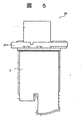
本実施例における物理量測定装置は、空気流量センサ6が実装されるプリント基板4と、プリント基板4が実装される支持体3とを備える。物理量測定装置20は、被測定媒体が流れる流路に取り付けるためのフランジ211を備る。フランジ211よりも首下(先端側)は、主流路に設けられた挿入穴から挿入されて片持ちで主流路に固定される。その結果、支持体3並びに支持体3に固定されるプリント基板4は、片持ちで固定される状態となっている。
プリント基板2と支持体3は、シリコーン接着剤2で接着されている。プリント基板2は、配線保護等のためにレジスト4でその表面が覆われている。そして、プリント基板2は、一部にレジスト4で覆われていない領域、言い換えるとプリント基板の基材(エポキシ樹脂)1が露出ざれている領域を有している。基材1が露出された領域にシリコーン接着2が配置され、プリント基板2と支持体3が固定されている。プリント基板4の一面側に流量センサ6が実装され、プリント基板4の他面側に基材露出部が形成されている。プリント基板4の他面側と支持体3が、シリコーン接着剤2により固定される。
流量センサ4は、ベアチップ(流量検出素子)であってもよいし、リードフレームと流量検出素子を樹脂で封止した樹脂パッケージでも良いし、金属や樹脂で形成される支持部材に流量検出素子を搭載した構造であってもよい。
支持体3の例として、アルミ等の金属材料で形成された金属プレートが挙げられる。基材露出部は、レジスト4を基材1に形成した後にエッチング等で除去する方法や、マスキングによりレジスト4が付着しないようにする方法で形成可能である。
次に本実施例の作用効果について説明する。プリント基板表面にレジストが付いた場合のシリコーン接着材と、プリント基板上にレジストを設けずに、基材(エポキシ樹脂)が露出された場合のシリコーン接着材の強度を評価した。その結果、基材が露出したものは、レジストがある場合に比べて約8倍の強度があることがわかった。また、レジストがある場合には、レジストとシリコーン接着材の界面から剥がれる界面破壊であるのに対して、基材にシリコーン接着材を接着した場合は、シリコーン接着材自体が破壊される母材破壊となることが分かった。一般的に接着強度は、界面破壊よりも母材破壊の方が強い。そのため、上記結果となる。
本実施例では、プリント基板の周囲のレジストを排除し、プリント基板の基材を露出させてシリコーン接着材と接着させたので、接着部の破壊は母材破壊となり強固な接着が可能となる。そのため、物理量測定装置の共振時の1500~2000Gの加速度にも耐えられる。
なお、実施例では加振力が高い物理量測定装置を示したが、プリント基板と支持体を強固に接着する場合に本方法は有効であることは言うまでもない。
なお、実施例では加振力が高い物理量測定装置を示したが、プリント基板と支持体を強固に接着する場合に本方法は有効であることは言うまでもない。
第2の実施例について図2を用いて説明する。実施例1と同様な構成については説明を省略する。なお、図2においては、シリコーン接着剤2はプリント基板4を透過した場合に見える状態を示している。
実施例1では、プリント基板4の他面の周縁に、囲うような形状で基材露出部(レジスト4のスリット、溝)が形成されているのに対して、本実施例では、プリント基板の他面の最外周に基材露出部を形成した。シリコーン接着剤2は、プリント基板の他面に形成された基材が露出された領域とプリント基板の側面(基材が露出)に接触している。
次に本実施例の作用効果について説明する。プリント基板4の端部はレジストを排除して基材が露出させている。さらに、プリント基板端部側面は切断により基材が露出されているので、この基材露出両面にシリコーン接着材を配置させることで、第一の実施例よりもより強固に接着をさせることが可能となる。
本発明の第3実施例について説明する。なお、実施例1若しくは2と同様の構成については説明を省略する。本実施例では、支持体にアルミを使用している。プリント基板とアルミの線膨張係数はそれぞれ、15E-6、24E-6/℃であり、その差は9E-6/℃となり大きい。
環境温度変化により、支持体であるアルミの変形につられてプリント基板も変形する。アルミとプリント基板の接着を柔らかいシリコーン接着材とすることで、上記変形を抑制できるので、支持体にアルミを使用した場合に特に本発明は好適である。アルミはGND電位に接続されていると、電磁シールド効果の観点から特に有効である。
環境温度変化により、支持体であるアルミの変形につられてプリント基板も変形する。アルミとプリント基板の接着を柔らかいシリコーン接着材とすることで、上記変形を抑制できるので、支持体にアルミを使用した場合に特に本発明は好適である。アルミはGND電位に接続されていると、電磁シールド効果の観点から特に有効である。
本発明の実施例4について図3を用いて説明する。実施例1から3の構成と同様の構成については説明を省略する。
本実施例では、シリコーン接着2と接着する露出領域の一部に、プリント基板配線10が形成されている。プリント基板配線とシリコーン接着材との破壊は界面破壊であるが、接着領域全体に比べ、配線とシリコーン接着材との接着領域はごく一部となるので、大きな影響はない。そのため、このようにシリコーン接着領域の一部に配線があっても差しつかえない。
当然ながらプリント基板中のスルーホール(図示しない)が、シリコーン接着材2の領域に存在しても大きな影響はないので問題ない。
当然ながらプリント基板中のスルーホール(図示しない)が、シリコーン接着材2の領域に存在しても大きな影響はないので問題ない。
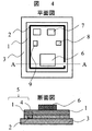
本発明の実施例5について図4を用いて説明する。実施例1から4と同様の構成については説明を省略する。
本実施例は、構成はほとんど第1の実施例と同じであるが、実施例1のシリコーン接着2領域の一部を排除した。接着強度の観点からは、プリント基板の周囲をシリコーン接着材で固定することが好ましいが、プリント基板周囲をシリコーン接着材で囲んだ場合には、囲まれた空気が密閉される。環境温度変化により、密閉された空気が膨張され、プリント基板の変形等が発生する場合がある。そのため、この場合には空気抜きを目的に、シリコーン接着2で完全に囲うのでななく、一部隙間を設けてることがより好ましい。本実施例では、シリコーン接着剤4が塗布される領域における隙間が一つの例を示したが、当然複数であってもよく、鎖線で囲うような形状であってもよい。また、強度が確保できるのであれば、囲う形状でなくともよく、複数点で接着する構造であっても、一点で接着する構造であってもよい。
1…プリント基板基材
2…シリコーン接着材
3…支持体
4…レジスト
5…プリント基板
6…空気流量センサ
7…圧力センサ
8…湿度センサ
9…温度センサ
10…配線
20…物理量測定装置
211…フランジ
2…シリコーン接着材
3…支持体
4…レジスト
5…プリント基板
6…空気流量センサ
7…圧力センサ
8…湿度センサ
9…温度センサ
10…配線
20…物理量測定装置
211…フランジ
Claims (9)
- プリント基板の基材に、シリコーン接着材が接することで、該プリント基板が支持体に固定される物理量測定装置。
- 前記シリコーン接着材は、少なくともプリント基板の周縁部で前記基材と接している請求項1に記載の物理量測定装置。
- 前記シリコーン接着剤は、プリント基板の最外周と、側面部で前記基材と接している請求項1に記載の物理量測定装置。
- 前記プリント基板は、基材表面上にレジストが形成されているレジスト形成部と、前記レジストが形成されずに前記基材が露出する露出部を備える請求項2または3に記載の物理量測定装置。
- 前記露出部は、囲うような形状である請求項4に記載の物理量測定装置。
- 前記シリコーン接着剤は、隙間を有しつつ、囲うように形成されている請求項4に記載の物理量測定装置。
- 前記支持体は、アルミベースである請求項3に記載の物理量測定装置。
- 前記プリント基板の一面に、流量センサ、圧力センサ、湿度センサ、温度センサの少なくとも1つが配置され、前記プリント基板の他面に前記露出部が形成されている請求項4に記載の物理量測定装置。
- 前記プリント基板を実装する支持体は、少なくとも1部が吸気管内に挿入される位置にある請求項8に記載の物理量測定装置
Applications Claiming Priority (2)
| Application Number | Priority Date | Filing Date | Title |
|---|---|---|---|
| JP2019001554A JP7218183B2 (ja) | 2019-01-09 | 2019-01-09 | 物理量測定装置 |
| JP2019-001554 | 2019-01-09 |
Publications (1)
| Publication Number | Publication Date |
|---|---|
| WO2020145032A1 true WO2020145032A1 (ja) | 2020-07-16 |
Family
ID=71521285
Family Applications (1)
| Application Number | Title | Priority Date | Filing Date |
|---|---|---|---|
| PCT/JP2019/048882 Ceased WO2020145032A1 (ja) | 2019-01-09 | 2019-12-13 | 物理量測定装置 |
Country Status (2)
| Country | Link |
|---|---|
| JP (1) | JP7218183B2 (ja) |
| WO (1) | WO2020145032A1 (ja) |
Citations (4)
| Publication number | Priority date | Publication date | Assignee | Title |
|---|---|---|---|---|
| JP2001257306A (ja) * | 2000-03-10 | 2001-09-21 | Denso Corp | 混成集積回路装置及びその製造方法 |
| JP2006303122A (ja) * | 2005-04-19 | 2006-11-02 | Citizen Electronics Co Ltd | チップ型led |
| JP2006310505A (ja) * | 2005-04-28 | 2006-11-09 | Citizen Electronics Co Ltd | 発光ダイオード |
| JP2008209243A (ja) * | 2007-02-27 | 2008-09-11 | Hitachi Ltd | 車載電子機器,車載物理量測定計および熱式空気流量計 |
Family Cites Families (2)
| Publication number | Priority date | Publication date | Assignee | Title |
|---|---|---|---|---|
| JPH04276686A (ja) * | 1991-03-04 | 1992-10-01 | Mitsubishi Cable Ind Ltd | 多層金属ベース基板 |
| JP5402107B2 (ja) * | 2009-03-10 | 2014-01-29 | 日本電気株式会社 | 半導体装置及びその製造方法 |
-
2019
- 2019-01-09 JP JP2019001554A patent/JP7218183B2/ja active Active
- 2019-12-13 WO PCT/JP2019/048882 patent/WO2020145032A1/ja not_active Ceased
Patent Citations (4)
| Publication number | Priority date | Publication date | Assignee | Title |
|---|---|---|---|---|
| JP2001257306A (ja) * | 2000-03-10 | 2001-09-21 | Denso Corp | 混成集積回路装置及びその製造方法 |
| JP2006303122A (ja) * | 2005-04-19 | 2006-11-02 | Citizen Electronics Co Ltd | チップ型led |
| JP2006310505A (ja) * | 2005-04-28 | 2006-11-09 | Citizen Electronics Co Ltd | 発光ダイオード |
| JP2008209243A (ja) * | 2007-02-27 | 2008-09-11 | Hitachi Ltd | 車載電子機器,車載物理量測定計および熱式空気流量計 |
Also Published As
| Publication number | Publication date |
|---|---|
| JP7218183B2 (ja) | 2023-02-06 |
| JP2020112379A (ja) | 2020-07-27 |
Similar Documents
| Publication | Publication Date | Title |
|---|---|---|
| US8643127B2 (en) | Sensor device packaging | |
| US8276460B2 (en) | Packaging for chip-on-board pressure sensor | |
| CN102401715B (zh) | 压力传感器 | |
| US7377177B1 (en) | Pressure sensor method and apparatus | |
| JP4281630B2 (ja) | センサ装置の製造方法 | |
| US8347707B2 (en) | Flow rate measuring apparatus | |
| CN111351612B (zh) | 压力传感器组件 | |
| JP3915605B2 (ja) | 圧力センサ装置 | |
| JP2018101684A (ja) | センサモジュールおよびその製造方法 | |
| US7320250B2 (en) | Pressure sensing element and sensor incorporating the same | |
| JP4968371B2 (ja) | センサデバイスの製造方法及びセンサデバイス | |
| JP7218183B2 (ja) | 物理量測定装置 | |
| JP4168813B2 (ja) | 圧力センサ装置 | |
| JP2008089421A (ja) | 圧力センサのパッケージ | |
| KR20110076539A (ko) | 압력 센서 및 그 제조 방법 | |
| US20200399118A1 (en) | Electronic device | |
| JP6507596B2 (ja) | 半導体センサ装置 | |
| JP4019966B2 (ja) | 圧力センサ装置 | |
| JP5920501B2 (ja) | センサデバイスの製造方法及びセンサデバイス | |
| JP5402863B2 (ja) | センサチップの実装構造およびその実装方法 | |
| JP6725852B2 (ja) | 半導体センサ装置 | |
| JP2014228295A (ja) | 半導体圧力センサ装置 | |
| JP6507595B2 (ja) | 半導体センサ装置 | |
| EP3225964B1 (en) | Semiconductor sensor device | |
| JP2012181198A (ja) | センサデバイスの製造方法及びセンサデバイス |
Legal Events
| Date | Code | Title | Description |
|---|---|---|---|
| 121 | Ep: the epo has been informed by wipo that ep was designated in this application |
Ref document number: 19909135 Country of ref document: EP Kind code of ref document: A1 |
|
| NENP | Non-entry into the national phase |
Ref country code: DE |
|
| 122 | Ep: pct application non-entry in european phase |
Ref document number: 19909135 Country of ref document: EP Kind code of ref document: A1 |