WO2020137663A1 - 撮像素子、撮像装置、撮像素子の作動方法、及びプログラム - Google Patents
撮像素子、撮像装置、撮像素子の作動方法、及びプログラム Download PDFInfo
- Publication number
- WO2020137663A1 WO2020137663A1 PCT/JP2019/049219 JP2019049219W WO2020137663A1 WO 2020137663 A1 WO2020137663 A1 WO 2020137663A1 JP 2019049219 W JP2019049219 W JP 2019049219W WO 2020137663 A1 WO2020137663 A1 WO 2020137663A1
- Authority
- WO
- WIPO (PCT)
- Prior art keywords
- image data
- output
- image
- frame rate
- processor
- Prior art date
- Legal status (The legal status is an assumption and is not a legal conclusion. Google has not performed a legal analysis and makes no representation as to the accuracy of the status listed.)
- Ceased
Links
Images














Classifications
-
- G—PHYSICS
- G02—OPTICS
- G02B—OPTICAL ELEMENTS, SYSTEMS OR APPARATUS
- G02B7/00—Mountings, adjusting means, or light-tight connections, for optical elements
- G02B7/02—Mountings, adjusting means, or light-tight connections, for optical elements for lenses
- G02B7/04—Mountings, adjusting means, or light-tight connections, for optical elements for lenses with mechanism for focusing or varying magnification
- G02B7/10—Mountings, adjusting means, or light-tight connections, for optical elements for lenses with mechanism for focusing or varying magnification by relative axial movement of several lenses, e.g. of varifocal objective lens
- G02B7/102—Mountings, adjusting means, or light-tight connections, for optical elements for lenses with mechanism for focusing or varying magnification by relative axial movement of several lenses, e.g. of varifocal objective lens controlled by a microcomputer
-
- G—PHYSICS
- G02—OPTICS
- G02B—OPTICAL ELEMENTS, SYSTEMS OR APPARATUS
- G02B7/00—Mountings, adjusting means, or light-tight connections, for optical elements
- G02B7/02—Mountings, adjusting means, or light-tight connections, for optical elements for lenses
- G02B7/14—Mountings, adjusting means, or light-tight connections, for optical elements for lenses adapted to interchange lenses
-
- G—PHYSICS
- G02—OPTICS
- G02B—OPTICAL ELEMENTS, SYSTEMS OR APPARATUS
- G02B7/00—Mountings, adjusting means, or light-tight connections, for optical elements
- G02B7/02—Mountings, adjusting means, or light-tight connections, for optical elements for lenses
- G02B7/04—Mountings, adjusting means, or light-tight connections, for optical elements for lenses with mechanism for focusing or varying magnification
- G02B7/08—Mountings, adjusting means, or light-tight connections, for optical elements for lenses with mechanism for focusing or varying magnification adapted to co-operate with a remote control mechanism
-
- G—PHYSICS
- G02—OPTICS
- G02B—OPTICAL ELEMENTS, SYSTEMS OR APPARATUS
- G02B7/00—Mountings, adjusting means, or light-tight connections, for optical elements
- G02B7/28—Systems for automatic generation of focusing signals
- G02B7/36—Systems for automatic generation of focusing signals using image sharpness techniques, e.g. image processing techniques for generating autofocus signals
- G02B7/38—Systems for automatic generation of focusing signals using image sharpness techniques, e.g. image processing techniques for generating autofocus signals measured at different points on the optical axis, e.g. focussing on two or more planes and comparing image data
-
- G—PHYSICS
- G03—PHOTOGRAPHY; CINEMATOGRAPHY; ANALOGOUS TECHNIQUES USING WAVES OTHER THAN OPTICAL WAVES; ELECTROGRAPHY; HOLOGRAPHY
- G03B—APPARATUS OR ARRANGEMENTS FOR TAKING PHOTOGRAPHS OR FOR PROJECTING OR VIEWING THEM; APPARATUS OR ARRANGEMENTS EMPLOYING ANALOGOUS TECHNIQUES USING WAVES OTHER THAN OPTICAL WAVES; ACCESSORIES THEREFOR
- G03B13/00—Viewfinders; Focusing aids for cameras; Means for focusing for cameras; Autofocus systems for cameras
- G03B13/02—Viewfinders
- G03B13/06—Viewfinders with lenses with or without reflectors
-
- H—ELECTRICITY
- H04—ELECTRIC COMMUNICATION TECHNIQUE
- H04N—PICTORIAL COMMUNICATION, e.g. TELEVISION
- H04N23/00—Cameras or camera modules comprising electronic image sensors; Control thereof
- H04N23/50—Constructional details
- H04N23/53—Constructional details of electronic viewfinders, e.g. rotatable or detachable
-
- H—ELECTRICITY
- H04—ELECTRIC COMMUNICATION TECHNIQUE
- H04N—PICTORIAL COMMUNICATION, e.g. TELEVISION
- H04N23/00—Cameras or camera modules comprising electronic image sensors; Control thereof
- H04N23/60—Control of cameras or camera modules
- H04N23/63—Control of cameras or camera modules by using electronic viewfinders
-
- H—ELECTRICITY
- H04—ELECTRIC COMMUNICATION TECHNIQUE
- H04N—PICTORIAL COMMUNICATION, e.g. TELEVISION
- H04N23/00—Cameras or camera modules comprising electronic image sensors; Control thereof
- H04N23/60—Control of cameras or camera modules
- H04N23/667—Camera operation mode switching, e.g. between still and video, sport and normal or high- and low-resolution modes
-
- H—ELECTRICITY
- H04—ELECTRIC COMMUNICATION TECHNIQUE
- H04N—PICTORIAL COMMUNICATION, e.g. TELEVISION
- H04N23/00—Cameras or camera modules comprising electronic image sensors; Control thereof
- H04N23/70—Circuitry for compensating brightness variation in the scene
- H04N23/73—Circuitry for compensating brightness variation in the scene by influencing the exposure time
-
- H—ELECTRICITY
- H04—ELECTRIC COMMUNICATION TECHNIQUE
- H04N—PICTORIAL COMMUNICATION, e.g. TELEVISION
- H04N23/00—Cameras or camera modules comprising electronic image sensors; Control thereof
- H04N23/80—Camera processing pipelines; Components thereof
-
- H—ELECTRICITY
- H04—ELECTRIC COMMUNICATION TECHNIQUE
- H04N—PICTORIAL COMMUNICATION, e.g. TELEVISION
- H04N23/00—Cameras or camera modules comprising electronic image sensors; Control thereof
- H04N23/95—Computational photography systems, e.g. light-field imaging systems
- H04N23/951—Computational photography systems, e.g. light-field imaging systems by using two or more images to influence resolution, frame rate or aspect ratio
-
- H—ELECTRICITY
- H04—ELECTRIC COMMUNICATION TECHNIQUE
- H04N—PICTORIAL COMMUNICATION, e.g. TELEVISION
- H04N25/00—Circuitry of solid-state image sensors [SSIS]; Control thereof
- H04N25/40—Extracting pixel data from image sensors by controlling scanning circuits, e.g. by modifying the number of pixels sampled or to be sampled
- H04N25/44—Extracting pixel data from image sensors by controlling scanning circuits, e.g. by modifying the number of pixels sampled or to be sampled by partially reading an SSIS array
-
- H—ELECTRICITY
- H04—ELECTRIC COMMUNICATION TECHNIQUE
- H04N—PICTORIAL COMMUNICATION, e.g. TELEVISION
- H04N25/00—Circuitry of solid-state image sensors [SSIS]; Control thereof
- H04N25/40—Extracting pixel data from image sensors by controlling scanning circuits, e.g. by modifying the number of pixels sampled or to be sampled
- H04N25/44—Extracting pixel data from image sensors by controlling scanning circuits, e.g. by modifying the number of pixels sampled or to be sampled by partially reading an SSIS array
- H04N25/441—Extracting pixel data from image sensors by controlling scanning circuits, e.g. by modifying the number of pixels sampled or to be sampled by partially reading an SSIS array by reading contiguous pixels from selected rows or columns of the array, e.g. interlaced scanning
-
- H—ELECTRICITY
- H04—ELECTRIC COMMUNICATION TECHNIQUE
- H04N—PICTORIAL COMMUNICATION, e.g. TELEVISION
- H04N25/00—Circuitry of solid-state image sensors [SSIS]; Control thereof
- H04N25/50—Control of the SSIS exposure
-
- G—PHYSICS
- G03—PHOTOGRAPHY; CINEMATOGRAPHY; ANALOGOUS TECHNIQUES USING WAVES OTHER THAN OPTICAL WAVES; ELECTROGRAPHY; HOLOGRAPHY
- G03B—APPARATUS OR ARRANGEMENTS FOR TAKING PHOTOGRAPHS OR FOR PROJECTING OR VIEWING THEM; APPARATUS OR ARRANGEMENTS EMPLOYING ANALOGOUS TECHNIQUES USING WAVES OTHER THAN OPTICAL WAVES; ACCESSORIES THEREFOR
- G03B17/00—Details of cameras or camera bodies; Accessories therefor
- G03B17/02—Bodies
- G03B17/12—Bodies with means for supporting objectives, supplementary lenses, filters, masks, or turrets
- G03B17/14—Bodies with means for supporting objectives, supplementary lenses, filters, masks, or turrets interchangeably
Definitions
- the technology of the present disclosure relates to an imaging device, an imaging device, an operation method of the imaging device, and a program.
- difference data between a first frame and a second frame is obtained, the difference data is output if no difference is detected, and the third data is output if a difference is detected.
- a technique for displaying an image corresponding to the imaged data of a frame on a display device is disclosed.
- Japanese Unexamined Patent Publication No. 2009-296353 discloses an image sensor module including a memory that stores captured image data as a digital signal, and a compression unit that compresses the captured image data read from the memory and outputs the compressed image data to the outside. ing.
- difference data between previously captured image data and current captured image data is used as compressed data.
- One embodiment according to the technology of the present disclosure is an imaging device and an imaging device capable of reducing the power consumption required to output image data, as compared with the case of outputting all image data obtained by being imaged.
- a method of operating an image sensor and a program are provided.
- An imaging device is an imaging device, stores image data obtained by imaging a subject at a first frame rate, and is built in the imaging device.
- the storage unit performs processing using the image data, and outputs the output image data based on the image data at the second frame rate based on the processing unit incorporated in the image sensor and the processing result of the processing unit.
- the processing unit includes an output unit built in the image pickup device, and the processing unit obtains first image data obtained as image data by being imaged and image data obtained before the first image data.
- the output unit outputs the output image data determined by the processing unit. As a result, it is possible to reduce the power consumption required to output the image data, as compared with the case of outputting all the image data obtained by being imaged.
- the processing unit performs thinning processing on the first image data and the second image data, and the first image data after the thinning processing and the first image data after the thinning processing are performed.
- the degree of difference from the two image data is derived.
- the processing unit detects the main subject image data indicating the image of the main subject from one of the first image data and the second image data, and calculates the first image data. From the other of the second image data and the second image data, the specific image data indicating the image identified from the position corresponding to the position of the image of the main subject in the image represented by the first image data is detected, and the degree of difference is determined by the processing unit. It is the degree of difference between the main subject image data detected by and the specific image data detected by the processing unit. As a result, it is possible to reduce the load on the processing unit as compared with the case where the difference between the entire first image data and the entire second image data is derived.
- the processing unit when the state in which the dissimilarity is less than the threshold value continues for a predetermined time, at least the first frame rate and the second frame rate. 1 Decrease the frame rate. As a result, it is possible to reduce the power consumption of the image sensor as compared with the case where imaging is performed without lowering the first frame rate during a period in which the subject is not noticeably moving.
- the processing unit detects the eye-closed image data indicating the image of the eye with the eyelids closed from the image data, and the output unit uses the processing unit to close the eye-closed image data.
- the image data in which the closed-eye image data is detected is not output. It is possible to reduce the power consumption required to output the image data, as compared with the case of outputting the output image data including the closed-eye image data.
- the output unit may include the first image data and the first image data if the closed eye image data is not detected by the processing unit when the difference is equal to or more than a threshold value. At least one of the two image data is determined as output image data. This makes it possible to provide the user with output image data that is expected to be highly necessary for the user.
- the processing unit derives an evaluation value indicating the degree of focusing on the image data, and the output unit sets the evaluation value derived by the processing unit to a predetermined value.
- the image data for which the evaluation value less than the default evaluation value is derived is not output.
- it is possible to reduce the power consumption required to output the image data, as compared with the case where the output image data corresponding to the focus evaluation value less than the predetermined evaluation threshold value is output.
- the processing unit when the dissimilarity is equal to or more than a threshold value, the first image data and the second image data on condition that the evaluation value is equal to or more than a predetermined evaluation value. At least one of the data is determined as output image data. This makes it possible to provide the user with output image data that is expected to be highly necessary for the user.
- the output unit outputs the first dummy data when the degree of difference is less than the threshold.
- the data toggle rate can be reduced as compared with the case where output image data is output when the difference is less than the threshold value.
- the output unit outputs the output image data when the output image data is the image data satisfying the specific condition even when the difference is equal to or more than the threshold value. No, the second dummy data is output. This makes it possible to reduce the data toggle rate as compared with the case where all the output image data is always output when the difference is equal to or more than the threshold value.
- the photoelectric conversion element and the storage unit are integrated into one chip.
- the portability of the image sensor can be improved as compared with the case where the photoelectric conversion element and the storage section are not integrated into one chip.
- the image sensor according to the twelfth aspect of the technology of the present disclosure is a stacked image sensor in which a storage unit is stacked on a photoelectric conversion element. As a result, it is possible to increase the transfer rate of data from the photoelectric conversion element to the storage section, as compared with a non-stacked image pickup element in which the storage section is not stacked on the photoelectric conversion element.
- An imaging device displays an image based on the image sensor according to any one of the first to twelfth aspects and output image data output by an output unit.
- a display control unit that controls the display of the unit.
- An imaging device stores an image sensor according to any one of the first to twelfth aspects, and output image data output by an output unit in a storage device. And a storage control unit for performing control. Thereby, power consumption can be reduced as compared with the case where all the image data obtained by capturing an image of a subject is stored in the storage device.
- a method of operating an image sensor performs a process using the storage unit that stores image data obtained by capturing an image of a subject at a first frame rate.
- Imaging including a processing unit and an output unit that outputs output image data based on the image data at a second frame rate based on a processing result in the processing unit, and includes a storage unit, a processing unit, and an output unit.
- the processing unit includes first image data obtained as image data by being imaged, and first image data obtained as image data before the first image data and stored in the storage unit.
- a program includes a storage unit that stores image data obtained by capturing an image of a subject at a first frame rate, a processing unit that performs processing using the image data, And an output unit that outputs output image data based on the image data at the second frame rate based on the processing result of the processing unit, and is included in the image sensor including the storage unit, the processing unit, and the output unit.
- the degree of difference with the second image data stored in the storage unit is derived, and when the derived degree of difference is equal to or more than a threshold value, at least one of the first image data and the second image data is used as output image data.
- the determining unit performs the determination process, and the output unit outputs the output image data determined by the processing unit. As a result, it is possible to reduce the power consumption required to output the image data, as compared with the case of outputting all the image data obtained by being imaged.
- An image sensor is an image sensor, stores image data obtained by capturing an image of a subject at a first frame rate, and is incorporated in the image sensor.
- a memory and a processor that performs processing using the image data, outputs output image data based on the image data at a second frame rate based on the processing result in the processing unit, and includes a processor incorporated in the image sensor.
- the processor includes the degree of difference between the first image data obtained as image data by being imaged and the second image data obtained as image data and stored in the memory before the first image data. If the derived degree of difference is equal to or greater than the threshold value, a process of determining at least one of the first image data and the second image data as output image data is performed, and the determined output image data is output.
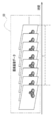
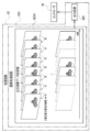
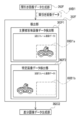
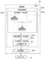
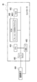
- FIG. 9 is a conceptual diagram for explaining an output frame rate of the image pickup apparatus according to the first to sixth embodiments. It is a block diagram showing an example of composition of a processing circuit contained in an image sensor of an imaging device concerning a 1st embodiment. It is a conceptual diagram with which the image data acquisition part shown in FIG. 8 is demonstrated. It is a conceptual diagram which shows an example of the output aspect of the captured image data output to the image data acquisition part from the memory shown in FIG.
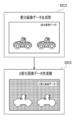
- FIG. 9 is a conceptual diagram for explaining the difference image data generation unit shown in FIG. 8.
- FIG. 9 is a conceptual diagram for explaining the difference image data generation unit and the binarized image data generation unit shown in FIG. 8.
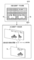
- FIG. 9 is a conceptual diagram for explaining a binarized image data generation unit and an output image data determination unit shown in FIG. 8.
- FIG. 14 is a conceptual diagram provided for detailed description of the output image data determination unit shown in FIGS. 8 and 13.
- 6 is a flowchart showing an example of the flow of an image pickup process according to the first embodiment.
- FIG. 9 is a conceptual diagram showing a modified example of image data output by an output circuit included in the processing circuit of the image pickup apparatus according to the first embodiment.
- 9 is a flowchart illustrating a modified example of the flow of the imaging process according to the first embodiment. It is a block diagram showing an example of composition of a processing circuit contained in an image sensor of an image pick-up device concerning a 2nd embodiment.
- FIG. 19 is a conceptual diagram for explaining the thinned-out image data generating unit and the difference image data generating unit shown in FIG. 18. It is a flow chart which shows an example of the flow of image pick-up processing concerning a 2nd embodiment. It is a block diagram showing an example of composition of a processing circuit contained in an image sensor of an image pick-up device concerning a 3rd embodiment.
- FIG. 23 is a conceptual diagram for explaining a thinned-out image data generation unit, a detection unit, and a difference image data generation unit illustrated in FIG. 22.
- FIG. 23 is a conceptual diagram provided for explaining the image processing circuit, the output circuit, and the controller shown in FIG. 22. It is a flow chart which shows an example of the flow of the imaging processing concerning a 3rd embodiment. It is a block diagram showing an example of composition of a processing circuit contained in an image sensor of an image pick-up device concerning a 4th embodiment. It is a block diagram showing an example of composition of a controller contained in an imaging device concerning a 4th embodiment. It is a functional block diagram which shows an example of the function of CPU of the controller contained in the imaging device which concerns on 4th Embodiment. It is a flow chart which shows an example of the flow of frame rate setting directions processing concerning a 4th embodiment.
- FIG. 33 is a conceptual diagram for explaining the output image data determination unit and the image data selection unit shown in FIG. 32.
- FIG. 34 is a conceptual diagram for explaining the image data selection unit shown in FIG. 33.
- FIG. 34 is a conceptual diagram provided for a detailed description of the image data selection unit shown in FIG. 33.
- FIG. 38 is a conceptual diagram for explaining the output image data determination unit and the image data selection unit shown in FIG. 37.
- FIG. 39 is a conceptual diagram provided for detailed description of the image data selection unit shown in FIG. 38. It is a conceptual diagram which shows an example of each data structure of the captured image data corresponding to a Bayer array, and thinned-out image data.
- the CPU refers to the abbreviation of "Central Processing Unit”.
- RAM refers to an abbreviation of “Random Access Memory”.
- ROM is an abbreviation for “Read Only Memory”.
- DRAM is an abbreviation of “Dynamic Random Access Memory”.
- SRAM refers to an abbreviation of “Static Random Access Memory”.
- the LSI is an abbreviation of “Large-Scale Integration”.
- ASIC is an abbreviation of “Application Specific Integrated Circuit”.
- PLD is an abbreviation for “Programmable Logic Device”.
- FPGA is an abbreviation for “Field-Programmable Gate Array”.
- SSD refers to the abbreviation of “Solid State Drive”.
- DVD-ROM is an abbreviation of "Digital Versatile Disc Read Only Memory”.
- USB is an abbreviation of “Universal Serial Bus”.
- HDD is an abbreviation for “Hard Disk Drive”.
- EEPROM is an abbreviation of “Electrically Erasable and Programmable Read Only Memory”.
- CCD is an abbreviation for “Charge Coupled Device”.
- CMOS is an abbreviation for “Complementary Metal Oxide Semiconductor”.
- EL means an abbreviation of "Electro-Luminescence”.
- A/D is an abbreviation for “Analog/Digital”.
- the FIFO means an abbreviation of “First in First out”.
- the I/F is an abbreviation of “Interface”.
- AF is an abbreviation for “Auto-Focus”.
- AE is an abbreviation for "Automatic Exposure”.
- the imaging device 10 is an interchangeable lens type camera.
- the imaging device 10 is a digital camera that includes an imaging device main body 12 and an interchangeable lens 14, and does not include a reflex mirror.
- a hybrid finder (registered trademark) 16 is provided in the imaging device body 12.
- the hybrid finder 16 referred to here is a finder in which, for example, an optical viewfinder (hereinafter referred to as “OVF”) and an electronic viewfinder (hereinafter referred to as “EVF”) are selectively used.
- OVF optical viewfinder
- EVF electronic viewfinder
- An image pickup element 44 is provided in the central portion of the image pickup apparatus main body 12 when viewed from the front.
- the image sensor 44 is, for example, a CMOS image sensor. Although described in detail later, the image sensor 44 is an example of a “multilayer image sensor” according to the technique of the present disclosure. Although a CMOS image sensor is illustrated as the image pickup element 44 here, the technique of the present disclosure is not limited to this, and for example, the technique of the present disclosure is established even when the image pickup element 44 is a CCD image sensor. ..
- the interchangeable lens 14 is replaceably attached to the imaging device body 12.
- An imaging lens 40 is provided on the lens barrel of the interchangeable lens 14.
- the optical axis L1 of the image pickup lens 40 is located at the center of the light receiving surface 44A of the image pickup element 44, and the subject light indicating the subject is received via the image pickup lens 40.
- An image is formed on the surface 44A.
- the interchangeable lens 14 is provided with a focus ring 13 used when the imaging device 10 is in the manual focus mode.
- the imaging lens 40 has a focus lens 40A, and the focus lens 40A moves in the optical axis direction in accordance with the manual rotation operation of the focus ring 13, and the focus lens 40A is moved to the light receiving surface 44A at a focus position according to the subject distance.
- the subject light is imaged.
- the "focus position" refers to the position on the optical axis L1 of the focus lens 40A in a focused state.
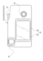
- a viewfinder switching lever 18 is provided on the front surface of the imaging device body 12.
- the optical image visible on the OVF and the live view image which is an electronic image visible on the EVF are switched by rotating the finder switching lever 18 in the arrow SW direction.
- the “live view image” referred to here is a moving image for display obtained by capturing an image of a subject by the image sensor 44.
- the live view image is also generally called a through image.
- a release button 20 and a dial 22 are provided on the upper surface of the imaging device body 12.
- the dial 22 is operated when setting the operation mode of the imaging system and the operation mode of the reproduction system.
- the release button 20 functions as an imaging preparation instruction unit and an imaging instruction unit, and can detect a two-step pressing operation of an imaging preparation instruction state and an imaging instruction state.
- the imaging preparation instruction state refers to, for example, a state of being pressed from the standby position to the intermediate position (half-pressed position), and the imaging instruction state is a state of being pressed to the final pressed position (full-pressed position) beyond the intermediate position. Refers to. In the following, the "state in which the standby position is pressed down to the half-pressed position" is referred to as the "half-pressed state", and the "state in which the standby position is pressed down to the fully-pressed position” is referred to as the "full-pressed state”.
- an image pickup mode and a reproduction mode are selectively set as operation modes according to a user's instruction.
- the imaging modes are roughly classified into a display moving image imaging mode and a recording imaging mode.
- an operation mode in which live view images for a plurality of consecutive frames obtained by continuous capturing are displayed on the first display 32 and/or the second display 86 (see FIG. 3) described later. is there.
- the recording image capturing mode is roughly classified into a still image capturing mode and a moving image capturing mode.
- the still image capturing mode is an operation mode in which a still image obtained by capturing an image of a subject by the image capturing apparatus 10 is recorded, and the moving image capturing mode is obtained by capturing an image of the subject in the image capturing apparatus 10. This is an operation mode for recording the captured moving image.
- the live view image is displayed on the first display 32 and/or the second display 86 described below, and the recording image data is recorded on the secondary storage device 80 (see FIG. 3) and/or the memory described below.
- the image data for recording is roughly classified into still image data and moving image data, the still image data is image data obtained in the still image capturing mode, and the moving image data is obtained in the moving image capturing mode. It is image data.
- the imaging device 10 When the imaging mode is set, the imaging device 10 first enters the display moving image imaging mode. In the display moving image capturing mode, when the release button 20 is pressed, the image capturing apparatus 10 shifts from the display moving image capturing mode to the recording capturing mode.
- manual focus mode and auto focus mode are selectively set according to the user's instruction.
- the release button 20 is half-pressed to adjust the imaging condition, and then, when the full-pressed state is continued, the exposure is performed. That is, when the release button 20 is half-pressed, the AE function works and the exposure state is set, then the AF function works and focus control is performed, and when the release button 20 is fully pressed, imaging is performed. ..
- a touch panel display 26, instruction keys 28, and a viewfinder eyepiece 30 are provided on the back surface of the imaging device body 12.
- the touch panel display 26 includes a first display 32 and a touch panel 34 (see also FIG. 3).
- the first display 32 may be a liquid crystal display or an organic EL display.
- the first display 32 displays images and character information.
- the first display 32 is used to display live view images obtained by continuous image capturing when the image capturing apparatus 10 is in the image capturing mode.
- the first display 32 is also used for displaying a still image obtained by being imaged when a still image imaging instruction is given. Further, the first display 32 is also used to display a reproduced image and a menu screen when the imaging device 10 is in the reproduction mode.
- the touch panel 34 is a transmissive touch panel, and is superimposed on the surface of the display area of the first display 32.
- the touch panel 34 detects, for example, contact with a finger or a pointer such as a stylus pen, and outputs the detection result to a predetermined output destination such as a CPU 46A (see FIG. 3) described later.
- the instruction key 28 receives various instructions such as selection of one or more menus, confirmation of selection, deletion of selection, zooming, and frame advance.
- the imaging device 10 includes mounts 36 and 38.
- the mount 36 is provided on the imaging device body 12.
- the mount 38 is provided at a position corresponding to the position of the mount 36 in the interchangeable lens 14.
- the interchangeable lens 14 is replaceably attached to the image pickup apparatus main body 12 by connecting the mount 38 to the mount 36.
- the interchangeable lens 14 has an imaging lens 40.
- the imaging lens 40 includes an objective lens 40B and a diaphragm 40C in addition to the focus lens 40A.
- the focus lens 40A, the objective lens 40B, and the diaphragm 40C are arranged in the order of the objective lens 40B, the focus lens 40A, and the diaphragm 40C along the optical axis L1 from the subject side to the imaging device body 12 side.
- the imaging lens 40 includes a slide mechanism 41 and motors 45 and 47.
- a motor 47 is connected to the diaphragm 40C, and the diaphragm 40C operates according to the power applied from the motor 47 to adjust the exposure.
- the slide mechanism 41 moves the focus lens 40A along the optical axis L1 by receiving power.
- the motor 45 and the focus ring 13 are connected to the slide mechanism 41, and the power from the motor 45 or the power obtained by operating the focus ring 13 is applied to the slide mechanism 41. That is, the slide mechanism 41 moves the focus lens 40A along the optical axis L1 according to the power from the motor 45 or the power obtained by operating the focus ring 13.
- the motors 45 and 47 are connected to the imaging device main body 12 via mounts 36 and 38, and the drive is controlled in accordance with a command from the imaging device main body 12.
- a stepping motor is applied as an example of the motor 45, 47. Therefore, the motors 45 and 47 operate in synchronization with the pulse power according to a command from the imaging device body 12.
- FIG. 3 an example in which the motors 45 and 47 are provided in the image pickup lens 40 is shown, but the present invention is not limited to this, and at least one of the motors 45 and 47 is the image pickup apparatus main body 12. May be provided.
- a rotary encoder 43 is provided in the imaging device body 12.
- the rotary encoder 43 is connected to the imaging device body 12 via mounts 36 and 38.
- the rotary encoder 43 detects the position of the focus ring 13 and outputs the detection result to the imaging device body 12.
- the image pickup apparatus main body 12 is provided with a mechanical shutter 42.
- the mechanical shutter 42 operates by receiving power from a drive source (not shown) such as a motor under the control of a CPU 46A described later.
- a drive source not shown
- the interchangeable lens 14 is attached to the imaging device main body 12 via the mounts 36 and 38, the subject light passes through the imaging lens 40 and is imaged on the light receiving surface 44A via the mechanical shutter 42.
- the image pickup apparatus main body 12 includes a controller 46 and a UI device 48.
- the controller 46 controls the entire imaging device 10.
- the UI device 48 is a device that presents information to the user and receives instructions from the user.
- a UI device 48 is connected to the controller 46 via a bus line 88, and the controller 46 acquires various information from the UI device 48 and controls the UI device 48.
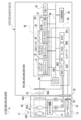
- the controller 46 includes a CPU 46A, a ROM 46B, a RAM 46C, a control I/F 46D, and an input I/F 46E.
- the CPU 46A, ROM 46B, RAM 46C, control I/F 46D, and input I/F 46E are connected to each other via a bus line 88.
- the CPU 46A reads various programs from the ROM 46B and expands the read various programs in the RAM 46C.
- the CPU 46A controls the entire imaging device 10 according to various programs loaded in the RAM 46C.
- the control I/F 46D is a device having an FPGA and is connected to the image pickup element 44.
- the CPU 46A controls the image sensor 44 via the control I/F 46D.
- the control I/F 46D is connected to the motors 45 and 47 via the mounts 36 and 38, and the CPU 46A controls the motors 45 and 47 via the control I/F 46D. Further, the control I/F 46D is connected to the rotary encoder 43 via the mounts 36 and 38, and the CPU 46A specifies the position of the focus ring 13 based on the detection result input from the rotary encoder 43.
- a secondary storage device 80 and an external I/F 82 are connected to the bus line 88.
- the secondary storage device 80 is a non-volatile memory such as a flash memory, SSD, HDD, or EEPROM.
- the CPU 46A reads/writes various information from/to the secondary storage device 80.
- the external I/F 82 is a device having an FPGA.
- An external device (not shown) such as a USB memory or a memory card is connected to the external I/F 82.
- the external I/F 82 controls the exchange of various information between the CPU 46A and the external device.
- the CPU 46A stores output image data 70 (see FIG. 6) described later in the secondary storage device 80 and/or the external device described above.
- the CPU 46A is an example of the “storage control unit” according to the technique of the present disclosure.
- the secondary storage device 80 and the external device are examples of the “storage device” according to the technology of the present disclosure.
- the UI device 48 includes the hybrid finder 16, the touch panel display 26, and the reception unit 84.
- the first display 32 and the touch panel 34 are connected to the bus line 88. Therefore, the CPU 46A causes the first display 32 to display various information and operates according to various instructions received by the touch panel 34.
- the reception unit 84 includes the touch panel 34 and the hard key unit 25.
- the hard key unit 25 is a plurality of hard keys, and has a release button 20, a dial 22, and an instruction key 28.
- the hard key unit 25 is connected to the bus line 88, and the CPU 46A operates according to various instructions received by the hard key unit 25.
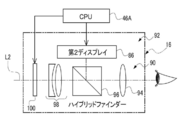
- the hybrid finder 16 has a second display 86.
- the CPU 46A causes the second display 86 to display various information.
- the hybrid finder 16 includes an OVF 90 and an EVF 92.
- the OVF 90 is an inverted Galileo finder and has an eyepiece lens 94, a prism 96, and an objective lens 98.
- the EVF 92 has a second display 86, a prism 96, and an eyepiece lens 94.
- a liquid crystal shutter 100 is disposed closer to the subject side than the objective lens 98 along the optical axis L2 of the objective lens 98, and when the EVF 92 is used, the liquid crystal shutter 100 does not cause an optical image to enter the objective lens 98. To block light.
- the prism 96 reflects the electronic image or various information displayed on the second display 86 and guides it to the eyepiece lens 94, and the optical image and the electronic image and/or various information displayed on the second display 86. To synthesize.
- a live view image is an example of the electronic image displayed on the second display 86.
- the CPU 46A controls the liquid crystal shutter 100 so that the liquid crystal shutter 100 is in a non-light-shielding state so that the optical image can be visually recognized from the eyepiece lens 94. Further, in the EVF mode, the CPU 46A controls the liquid crystal shutter 100 so that the liquid crystal shutter 100 is in a light-shielding state so that only the electronic image displayed on the second display 86 can be viewed from the eyepiece lens 94.
- the first display 32 (see FIG. 3) and the second display 86 will be referred to as “displays” without reference numerals unless it is necessary to describe them separately.
- the display is an example of a “display unit” according to the technology of the present disclosure.
- the CPU 46A is an example of the “display control unit” according to the technique of the present disclosure.
- the image sensor 44 includes a photoelectric conversion element 61, a processing circuit 62, and a memory 64.
- the processing circuit 62 and the memory 64 are stacked on the photoelectric conversion element 61.
- the image pickup element 44 is an image pickup element in which the photoelectric conversion element 61, the processing circuit 62, and the memory 64 are integrated into one chip. That is, the photoelectric conversion element 61, the processing circuit 62, and the memory 64 are packaged in one package.
- the photoelectric conversion element 61 and the processing circuit 62 are electrically connected to each other by conductive bumps (not shown) such as copper
- the processing circuit 62 and the memory 64 are also conductive such as copper. Are electrically connected to each other by bumps (not shown) having a.
- the memory 64 is an example of a “storage unit” according to the technique of the present disclosure.
- the processing circuit 62 is, for example, an LSI, and the memory 64 is, for example, a DRAM.
- the technique of the present disclosure is not limited to this, and SRAM may be adopted as the memory 64 instead of DRAM.
- the processing circuit 62 is realized by ASIC and FPGA, and exchanges various information with the controller 46.
- the processing circuit 62 may be realized by only an ASIC, PLD, or FPGA, or may be realized by a combination of ASIC and PLD or a combination of PLD and FPGA among ASIC, PLD, and FPGA.
- a computer including a CPU, a ROM, and a RAM may be adopted. The CPU may be singular or plural.
- the processing circuit 62 may be realized by a combination of hardware configuration and software configuration.
- the photoelectric conversion element 61 has a plurality of photodiodes arranged in a matrix.
- An example of the plurality of photodiodes is a photodiode for “4896 ⁇ 3265” pixels.
- the photoelectric conversion element 61 includes a color filter, and the color filter includes a G filter corresponding to G (green) that most contributes to obtain a luminance signal, an R filter corresponding to R (red), and a B (blue) filter. ) Corresponding to the B filter.
- the G filter, the R filter, and the B filter are arranged in the row direction (horizontal direction) and the column direction (vertical direction) with a predetermined periodicity for the plurality of photodiodes of the photoelectric conversion element 61. ing. Therefore, the imaging device 10 can perform processing in accordance with a repeating pattern when performing demosaicing processing of R, G, and B signals.
- the demosaic process refers to a process of calculating all color information for each pixel from a mosaic image corresponding to the color filter array of the single-plate color image sensor.
- the demosaic process means a process of calculating color information of all RGB for each pixel from a mosaic image of RGB.
- the image pickup element 44 has a so-called electronic shutter function, and by operating the electronic shutter function under the control of the controller 46, the charge storage time of each photodiode in the photoelectric conversion element 61 is controlled.
- the charge storage time refers to so-called shutter speed.
- the image capturing apparatus 10 uses a rolling shutter method to capture a still image and a moving image. Imaging for a still image is realized by activating the electronic shutter function and actuating the mechanical shutter 42 (see FIG. 3), and imaging for a live view image is performed without operating the mechanical shutter 42. It is realized by activating a function.
- the rolling shutter method is illustrated here, the technology of the present disclosure is not limited to this, and a global shutter method may be applied instead of the rolling shutter method.
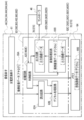
- the processing circuit 62 includes a reading circuit 62A, a digital processing circuit 62B, an image processing circuit 62C, an output circuit 62D, and a control circuit 62E.
- the readout circuit 62A, the digital processing circuit 62B, the image processing circuit 62C, and the control circuit 62E are realized by ASIC, and the output circuit 62D is realized by FPGA.
- the image processing circuit 62C is an example of the “processing unit” according to the technology of the present disclosure
- the output circuit 62D is an example of the “output unit” according to the technology of the present disclosure.
- the control circuit 62E is connected to the controller 46. Specifically, the control circuit 62E is connected to the control I/F 46D (see FIG. 3) of the controller 46, and controls the entire imaging element 44 according to the instruction of the CPU 46A (see FIG. 3).
- the read circuit 62A is connected to the photoelectric conversion element 61, the digital processing circuit 62B, and the control circuit 62E.
- the memory 64 is connected to the digital processing circuit 62B, the image processing circuit 62C, and the control circuit 62E.
- the image processing circuit 62C is connected to the output circuit 62D, the control circuit 62E, and the memory 64.
- the output circuit 62D is connected to the control circuit 62E and the controller 46. Specifically, the output circuit 62D is connected to the input I/F 46E (see FIG. 3) of the controller 46.
- the reading circuit 62A reads the analog captured image data 69A, which is the signal charge accumulated in the photoelectric conversion element 61, from the photoelectric conversion element 61. Specifically, the reading circuit 62A reads the picked-up image data 69A for each frame according to the vertical synchronization signal input from the control circuit 62E. Further, the reading circuit 62A reads the picked-up image data 69A row by row according to the horizontal synchronizing signal input from the control circuit 62E within the reading period of one frame.
- the digital processing circuit 62B digitally converts the analog captured image data 69A by performing signal processing of correlated double sampling on the analog captured image data 69A read by the readout circuit 62A and then performing A/D conversion. Turn into. Then, the digital processing circuit 62B stores the captured image data 69B obtained by digitizing the captured image data 69A in the memory 64. In the following description, the captured image data 69A and 69B will be referred to as "captured image data 69" unless it is necessary to distinguish between them.
- the memory 64 is a memory capable of storing captured image data 69B of multiple frames.
- the memory 64 has a storage area (not shown) for each pixel, and the captured image data 69B is stored in the corresponding storage area of the memory 64 for each pixel by the digital processing circuit 62B.
- the image processing circuit 62C performs processing using the captured image data 69B. Specifically, the image processing circuit 62C acquires the captured image data 69B from the memory 64, and performs various signal processes on the acquired captured image data 69B.
- the “various signal processing” mentioned here includes known signal processing such as color tone correction, white balance adjustment, sharpness adjustment, gamma correction, and gradation correction, and also includes signal processing according to the technology of the present disclosure. Be done.
- the signal processing according to the technique of the present disclosure includes, for example, the image data acquisition unit 62C1, the difference image data generation unit 62C2, the binarized image data generation unit 62C3, and the output image data determination illustrated in FIG. This indicates signal processing by the unit 62C4.
- the image processing circuit 62C generates output image data 70 by performing various kinds of signal processing on the captured image data 69A, and outputs the generated output image data 70 to the output circuit 62D.
- the output circuit 62D outputs the output image data 70 based on the captured image data 69B based on the result of various signal processings in the image processing circuit 62C. Specifically, the output circuit 62D outputs the output image data 70 input from the image processing circuit 62C to the controller 46.
- the image pickup element 44 picks up an image of a subject at the image pickup frame rate, and outputs the output image data 70 to the controller 46 at the output frame rate.
- the imaging frame rate is an example of the “first frame rate” according to the technology of the present disclosure
- the output frame rate is an example of the “second frame rate” according to the technology of the present disclosure.
- imaging refers to a process from the start of exposure of one frame in the photoelectric conversion element 61 to the storage of one frame of captured image data 69B in the memory 64.
- the imaging frame rate is a frame rate required for imaging performed by the photoelectric conversion element 61, the readout circuit 62A, the digital processing circuit 62B, the control circuit 62E, and the memory 64 in cooperation with each other.
- the output frame rate is the same as the frame rate used by the device in the subsequent stage of the image sensor 44.
- the imaging frame rate and the output frame rate need only have a relationship of “imaging frame rate ⁇ output frame rate”.
- the imaging frame rate is a frame rate at which imaging for 8 frames is performed within the period T
- the output frame rate is 3 frames within the period T as shown in FIG. 7B. It suffices as long as it is the frame rate at which
- 240 fps (frames per second) is adopted as the imaging frame rate and 60 fps is adopted as the output frame rate, but the technique of the present disclosure is not limited to this.
- 300 fps may be adopted as the imaging frame rate and 120 fps may be adopted as the output frame rate, or the imaging frame rate and the output frame rate may be the same.
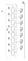
- the image processing circuit 62C includes an image data acquisition unit 62C1, a difference image data generation unit 62C2, a binarized image data generation unit 62C3, and an output image data determination unit 62C4.
- the image data acquisition unit 62C1 is connected to the memory 64.
- the difference image data generation unit 62C2 is connected to the image data acquisition unit 62C1.
- the binarized image data generation unit 62C3 is connected to the difference image data generation unit 62C2.
- the output image data determination unit 62C4 is connected to the binarized image data generation unit 62C3.
- the output circuit 62D is connected to the output image data determination unit 62C4.
- the image data acquisition unit 62C1 acquires the captured image data 69B from the memory 64.
- the latest frame image data and the past frame image data are acquired by the image data acquisition unit 62C1 as the captured image data 69B.
- the memory 64 inputs/outputs the captured image data 69B by the FIFO method, and the image data acquisition unit 62C1 sequentially acquires the captured image data 69B output from the memory 64.
- the image data acquisition unit 62C1 temporarily holds a pair of captured image data 69B sequentially acquired from the memory 64.
- the latest captured image data 69B acquired from the memory 64 is the latest frame image data described above.
- the captured image data 69B acquired from the memory 64 one frame before the latest frame image data is the above-mentioned past frame image data.
- the captured image data 69B is input/output to/from the memory 64 by the FIFO method, and the image data acquisition unit 62C1 stores the captured image data 69B in the memory 64 from the memory 64 each time.
- the output captured image data 69B is acquired.
- the image data acquisition unit 62C1 temporarily holds a pair of captured image data 69B acquired from the memory 64 and having adjacent timings.
- the image data acquisition unit 62C1 outputs the past frame image data when the new captured image data 69B is acquired from the memory 64. Further, when the image data acquisition unit 62C1 acquires new captured image data 69B from the memory 64, it holds the latest frame image data as a past frame image and holds the newly acquired captured image data 69B as the latest frame image data. .. As described above, every time the image data acquisition unit 62C1 acquires the captured image data 69B from the memory 64, the pair of captured image data 69B held by the image data acquisition unit 62C1 is updated.
- the captured image data 69B output from the image data acquisition unit 62C1 is input to the difference image data generation unit 62C2.
- the differential image data generation unit 62C2 acquires the captured image data 69B from the image data acquisition unit 62C1 and holds it as the latest frame image data and the past frame image data, like the image data acquisition unit 62C1. Further, when the difference image data generation unit 62C2 newly acquires the captured image data 69B from the image data acquisition unit 62C1, the difference image data generation unit 62C2 updates the latest frame image data and the past frame image data to be held, like the image data acquisition unit 62C1. The captured image data 69B held as the past frame image data is output to the binarized image data generation unit 62C3 (see FIGS. 8 and 12).
- the differential image data generation unit 62C2 uses the pair of captured image data 69B currently held, that is, the absolute value of the difference between the latest frame image data and the past frame image data (hereinafter, referred to as “difference absolute value”). Calculate and generate difference image data by the difference absolute value.
- difference absolute value the absolute value of the difference between the latest frame image data and the past frame image data
- the difference image data I diff (x, y) is expressed by the following equation (1). ).
- I diff (x, y)
- Differential image data generating unit 62C2 the difference image data I diff (x, y) when calculating the calculated difference image data I diff (x, y) output in the binary image data generation unit 62C3 (see FIG. 12) To do.
- the binarized image data generation unit 62C3 acquires the difference image data from the difference image data generation unit 62C2 and generates the binarized image data from the acquired difference image data.
- the binarized image data generation unit 62C3 binarizes the difference image data I diff (x, y).
- the difference image data I diff (x, y) is converted into the binarized image data I bin (x, y) according to the following equations (2) and (3).
- the captured image data 69B output from the difference image data generation unit 62C2 is input to the binarized image data generation unit 62C3.
- the binarized image data generation unit 62C3 acquires the captured image data 69B from the difference image data generation unit 62C2 and holds it as the latest frame image data and the past frame image data, like the image data acquisition unit 62C1. Further, when the binarized image data generation unit 62C3 newly acquires the captured image data 69B from the difference image data generation unit 62C2, like the image data acquisition unit 62C1, the latest frame image data and the past frame image data to be held are retained. Is updated and the captured image data 69B held as the past frame image data is output to the output image data determination unit 62C4 (see FIG. 8).
- the output image data determination unit 62C4 is used to generate the binarized image data including the binarized difference region S A and the binarized difference region S B when the calculated total area is equal to or larger than the predetermined area.
- the latest frame image data among the latest frame image data and the past frame image data is determined as the output image data 70.
- predetermined area is, for example, the area of the binarized difference region in the case where it is possible to visually recognize that the subject is moving while the imaging for two frames is performed. And/or the area obtained from the results of sensory tests using an actual machine. In the first embodiment, 20% of the area of the entire image represented by the binarized image data is adopted as the "predetermined area".
- the above “predetermined area” may be a variable value that can be changed according to an instruction received by the receiving unit 84 (see FIG. 3) or a fixed value.
- predetermined area is an example of “threshold value” according to the technology of the present disclosure
- total area of the binarized difference area S A and the binarized difference area S B is “difference” according to the technology of the present disclosure. Is an example of “degree”.
- the total area of the binarized difference region S A and the binarized difference region S B is also simply referred to as “the area of the binarized difference region”.
- the output image data determination unit 62C4 performs binarization corresponding to the input captured image data 69B each time the captured image data 69B is input from the binarized image data generation unit 62C3. The total area of the binary difference area of the image data is compared with the predetermined area. The output image data determination unit 62C4 determines whether to output the input captured image data 69B to the output circuit 62D based on the comparison result. Then, the output image data determination unit 62C4 sequentially outputs the output image data 70 determined as the captured image data 69B to be output to the output circuit 62D.
- the output circuit 62D outputs the image data at the output frame rate based on the processing result of the image processing circuit 62C. Specifically, the output circuit 62D outputs the output image data 70 based on the captured image data 69B at the output frame rate based on the processing result obtained by processing the captured image data 69B by the image processing circuit 62C.
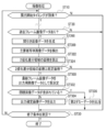
- step ST10 the readout circuit 62A determines whether or not the timing to start exposure of the photoelectric conversion element 61 (hereinafter, referred to as “exposure start timing”) has arrived. To do.
- the exposure start timing is a timing that is periodically defined by the above-described image pickup frame rate.
- step ST10 if the exposure start timing has not come, the determination is negative, and the imaging process moves to step ST30.
- step ST10 if the exposure start timing has come, the determination is affirmative and the imaging process moves to step ST12.
- step ST12 the readout circuit 62A causes the photoelectric conversion element 61 to perform exposure for one frame.
- the readout circuit 62A reads out one frame of captured image data 69A from the photoelectric conversion element 61.
- the digital processing circuit 62B performs signal processing of correlated double sampling on the captured image data 69A read in step ST14 and then performs A/D conversion to obtain the captured image data 69A. Digitize.
- the digital processing circuit 62B stores the captured image data 69B obtained by digitization in the memory 64.
- the captured image data 69B stored in the memory 64 is acquired by the image data acquisition unit 62C1.
- the image data acquisition unit 62C1 determines whether or not it has past frame image data. That is, the image data acquisition unit 62C1 determines whether or not a pair of captured image data 69B including the latest frame image data and the past frame image data is held. If the previous frame image data is not included in step ST20, the determination is negative, and the imaging process proceeds to step ST30. If the past frame image data is included in step ST20, the determination is affirmative, and the imaging process proceeds to step ST22.
- step ST22 first, the difference image data generation unit 62C2 calculates a difference absolute value between the latest frame image data acquired by the image data acquisition unit 62C1 and the past frame image data, and the above-mentioned difference is calculated from the calculated difference absolute value. Generate image data.
- the binarized image data generation unit 62C3 binarizes the difference image data to generate the binarized image data described above.
- the output image data determination unit 62C4 calculates the above-described binarized difference area from the binarized image data value generated by the binarized image data generation unit 62C3.
- the output image data determination unit 62C4 determines whether or not the area of the binarized difference region is equal to or larger than the above-mentioned predetermined area. When the area of the binarized difference region is not equal to or larger than the predetermined area in step ST24, the determination is negative and the imaging process proceeds to step ST30. If the area of the binarized difference region is equal to or larger than the predetermined area in step ST24, the determination is affirmative and the imaging process proceeds to step ST26.
- step ST26 the output image data determination unit 62C4 outputs the latest frame image data of the latest frame image data and the past frame image data used to generate the binarized image data including the binarized difference area as the output image data. It is determined as 70.
- the output circuit 62D outputs the output image data 70 determined in step ST26 to the controller 46.
- the controller 46 causes the output image data 70 input from the output circuit 62D to be displayed on the display as a live view image or a still image, or to be stored in the secondary storage device 80 and/or a memory card (not shown). ..
- step ST30 the control circuit 62E determines whether or not a condition for ending the imaging process (hereinafter, referred to as “imaging process end condition”) is satisfied.
- the image capturing process end condition include a condition that an instruction to end the image capturing process is received by the receiving unit 84.
- the determination is negative and the image capturing process proceeds to step ST10.
- the image capturing process end condition is satisfied, the image capturing process ends.
- the image sensor 44 includes the memory 64, the image processing circuit 62C, and the memory 64.
- the memory 64 stores captured image data 69B obtained by capturing an image of a subject at an image capturing frame rate.
- the image processing circuit 62C calculates the degree of difference between the latest frame image data, which is a pair of captured image data 69B, and the past frame image data.
- the dissimilarity refers to the area of the binarized difference region described above. Since the larger the area of the binarization difference area is, the larger the movement of the subject is. Therefore, the captured image data 69 obtained by capturing the image at this time can be displayed or stored by the user. It is expected to be worthy image data. On the other hand, the smaller the area of the binarized difference region, the smaller the motion of the subject. Therefore, the captured image data 69 obtained by being captured at this time is displayed or stored by the user. It is expected that the image data is unworthy of use.
- the image processing circuit 62C when the area of the binarized difference region is equal to or larger than the predetermined threshold value, the latest frame image data used for calculating the dissimilarity is determined as the output image data 70. Then, the output image data 70 is output to the controller 46 by the output circuit 62D. As a result, it is possible to reduce the power consumption required to output the image data, as compared with the case of outputting all the image data obtained by being imaged.
- the image pickup element 44 is an image pickup element in which the photoelectric conversion element 61, the processing circuit 62, and the memory 64 are integrated into one chip.
- the portability of the image pickup device 44 is higher than that of the image pickup device in which the photoelectric conversion element 61, the processing circuit 62, and the memory 64 are not integrated into one chip.
- the degree of freedom in design can be increased as compared with an image pickup device in which the photoelectric conversion element 61, the processing circuit 62, and the memory 64 are not integrated into one chip.
- the photoelectric conversion element 61, the processing circuit 62, and the memory 64 can contribute to downsizing of the image pickup apparatus main body 12 as compared with an image pickup element in which one chip is not formed.
- the image pickup element 44 a laminated type image pickup element in which a memory 64 is laminated on a photoelectric conversion element 61 is adopted.
- the transfer speed of the captured image data 69 from the photoelectric conversion element 61 to the memory 64 can be increased as compared with the case where the photoelectric conversion element 61 and the memory 64 are not stacked.
- the improvement of the transfer speed also contributes to the speeding up of the processing in the processing circuit 62 as a whole.
- the degree of freedom in design can be increased as compared with the case where the photoelectric conversion element 61 and the memory 64 are not stacked.
- a live view image or the like based on the output image data 70 is displayed on the second display 86.
- the user can visually recognize the image represented by the output image data 70.
- power consumption can be reduced as compared with the case where all the captured image data 69B obtained by capturing an image of a subject are displayed on the display. Further, it is possible to allow the user to visually recognize only the image that is expected to be highly necessary for the user.
- the output image data 70 is stored in the secondary storage device 80 and/or a memory card or the like. This makes the storage capacity of the secondary storage device 80 and/or the memory card last longer than in the case where all the captured image data 69B obtained by capturing an image of a subject is stored in the secondary storage device 80 or the like. be able to.
- the latest frame image data that has not been determined as the output image data 70 in step ST26 has been described with reference to an example in which the output circuit 62D does not output the latest frame image data to the controller 46.
- the latest frame image data and the past frame image used to generate the binarized image data including the binarized difference region may be output instead of the latest frame image data of the data. That is, the output circuit 62D may output the dummy data 70a to the controller 46 instead of the latest frame image data that has not been determined as the output image data 70 in step ST26 of the above-described imaging process.
- Examples of the dummy data 70a include image data having the same pixel value for all pixels.
- the image data having the same pixel value for all pixels refers to, for example, image data for which the pixel values for all pixels are “0”.
- the processing circuit 62 executes the imaging process shown in FIG. 17 as an example.
- the image capturing process proceeds to step ST32.
- the output circuit 62D outputs the dummy data 70a to the controller 46, and then the imaging process proceeds to step ST30.
- the dummy data 70a is output to the controller 46 by the output circuit 62D.
- the area of the binarized difference region is smaller than the predetermined area means that the captured image data 69 obtained by being imaged at this time is image data that is not worth displaying or storing to the user. Expected to be.
- the degree of change in the data between the image pickup element 44 and the controller 46 that is, the toggle rate of the data, is set, as compared with the case where no image data is simply output. Can be made smaller.
- the dummy data 70a is an example of “first dummy data” according to the technique of the present disclosure.
- the area of the binarized difference region is illustrated as an example of the “difference degree” according to the technology of the present disclosure, but the technology of the present disclosure is not limited to this.
- the absolute value of a simple difference between the latest frame image data and the past frame image data may be applied instead of the area of the binarized difference region.
- the difference absolute value is exemplified, but the present invention is not limited to this, and may be the ratio of the latest frame image data to the past frame image data.
- the ratio of the latest frame image data to the past frame image data refers to, for example, “I past (x, y)/I curr (x, y)”.
- the pair of captured image data 69A is stored in the memory 64
- the technique of the present disclosure is not limited to this.
- the latest frame image data to be compared with the past frame image data may be directly output from the digital processing circuit 62B to the image processing circuit 62C without being stored in the memory 64.
- the captured image data 69B is input to the memory 64 for each frame as past frame image data from the digital processing circuit 62B.
- the image processing circuit 62C calculates the degree of difference between the captured image data 69B input as the past frame image data from the memory 64 and the latest frame image data directly input from the digital processing circuit 62B.
- the past frame image data is the captured image data 69B one frame before the latest frame image data, but the technique of the present disclosure is not limited to this.
- the past frame image data may be the captured image data 69B two frames or more before the latest frame image data.
- the live view image and the like based on the output image data 70 is displayed on the second display 86, but the technique of the present disclosure is not limited to this.
- a live view image or the like based on the output image data 70 may be displayed on the first display 32, or may be displayed on both the first display 32 and the second display 86.
- the image pickup element 44 is an image pickup element in which the photoelectric conversion element 61, the processing circuit 62, and the memory 64 are integrated into one chip, but the technique of the present disclosure is not limited to this.
- the photoelectric conversion element 61 and the memory 64 among the photoelectric conversion element 61, the processing circuit 62, and the memory 64 may be integrated into one chip.
- an imaging device 200 has an imaging device main body 212 instead of the imaging device main body 12 as compared with the imaging device 10 described in the first embodiment. It has different points.
- the image pickup apparatus main body 212 is different from the image pickup apparatus main body 12 in that an image pickup element 244 is provided instead of the image pickup element 44.
- the image pickup element 244 differs from the image pickup element 44 in that the image pickup element 244 includes a processing circuit 262 instead of the processing circuit 62.
- the processing circuit 262 has an image processing circuit 262C in place of the image processing circuit 62C and an output circuit 262D in place of the output circuit 62D, as compared with the processing circuit 62. different.
- the image processing circuit 262C differs from the image processing circuit 62C in that the output image data 70 is generated based on the captured image data 69B instead of generating the output image data 70 based on the captured image data 69B.
- the output circuit 262D is different from the output circuit 62D in that it outputs the output image data 270 instead of the output image data 70.
- the image processing circuit 262C includes an image data acquisition unit 262C1, a thinned-out image data generation unit 262F, a difference image data generation unit 262C2, a binarized image data generation unit 262C3, and an output image data determination unit. 262C4.
- the image data acquisition unit 262C1 acquires the captured image data 69B from the memory 64, similarly to the image data acquisition unit 62C1 of the first embodiment. That is, the image data acquisition unit 262C1 acquires the latest frame image data and the past frame image data from the memory 64, similarly to the image data acquisition unit 62C1 of the first embodiment.
- the thinned-out image data generation unit 262F performs thinning-out processing on the captured image data 69B acquired by the image data acquisition unit 262C1. Specifically, the thinned-out image data generation unit 262F performs thinning-out processing on each of the latest frame image data and the past frame image data acquired by the image data acquisition unit 262C1.
- the thinning-out process is a process of compressing the captured image data 69B by thinning out pixels from the captured image data 69B.
- the difference image data generation unit 262C2 differs from the difference image data generation unit 62C2 described in the first embodiment in that difference image data is generated from the thinned image data 69B1 instead of the captured image data 69B.
- the binarized image data generation unit 262C3 is different from the binarized image data generation unit 62C3 described in the first embodiment, in place of the difference image data generated by the difference image data generation unit 62C2.
- the difference is that binarized image data is generated from the difference image data generated by the H.262C2.
- the output image data determination unit 262C4 compares the output image data 70 based on the binarized image data generated by the binarized image data generation unit 62C3, as compared with the output image data determination unit 62C4 described in the first embodiment. Instead of determining, the output image data 270 is generated based on the binarized image data generated by the binarized image data generation unit 262C3.
- the output image data determination unit 262C4 outputs the output image data 270 to the output circuit 262D.
- the output image data 270 is different from the output image data 70 in that it is not the latest frame image data of the captured image data 69B but the latest frame image data after thinning processing.
- the captured image data 69B is color image data having R pixels, G pixels, and B pixels.
- the captured image data 69B is image data in which a plurality of primary color pixels are arranged periodically. Specifically, in the captured image data 69B, R pixels, G pixels, and B pixels are arrayed in a periodicity corresponding to the X-Trance (registered trademark) array.
- the R pixels, the G pixels, and the B pixels are arranged in the row direction in the order of G pixels, B pixels, R pixels, G pixels, and R pixels in this order. ..
- the R pixels, the G pixels, and the B pixels are arranged in the row direction so as to circulate in the order of the R pixels, the G pixels, the G pixels, the B pixels, the G pixels, and the G pixels.
- the R pixels, the G pixels, and the B pixels are arranged in the row direction so as to circulate in the order of the B pixels, the G pixels, the G pixels, the R pixels, the G pixels, and the G pixels.
- the R pixels, the G pixels, and the B pixels are arranged in the row direction so as to circulate in the order of the G pixels, the R pixels, the B pixels, the G pixels, the B pixels, and the R pixels.
- the R pixels, the G pixels, and the B pixels are arranged in the row direction in the order of B pixels, G pixels, G pixels, R pixels, G pixels, and G pixels in this order.
- R pixels, G pixels, and B pixels are arranged in the row direction in the order of R pixels, G pixels, G pixels, B pixels, G pixels, and G pixels in this order.
- the arrangement pattern of the R pixels, G pixels, and B pixels in the first row to the sixth row is repeated in the column direction in units of 6 rows, whereby the entire R pixels, G pixels, and B pixels of the captured image data 69B.
- Array pattern is formed.
- the thinned-out image data 69B1 is image data obtained by subjecting the captured image data 69B to thinning processing in units of lines. Specifically, as shown in FIG. 19 as an example, the thinned-out image data 69B1 is a vertical 1/2 obtained by thinning out pixels of even-numbered lines in the column direction from the captured image represented by the captured image data 69B. It is image data showing a thinned image. That is, the pixels in each row of the vertical 1/2 thinned-out image are pixels corresponding to the pixels in the odd-numbered row of the captured image.
- the difference image data generation unit 262C2 acquires the thinned image data 69B1 from the thinned image data generation unit 262F.
- the thinned-out image data 69B1 is generated by the thinned-out image data generation unit 262F performing thinning processing on a line-by-line basis for each of the latest frame image data and the past frame image data. That is, the thinned-out image data 69B1 is the latest frame image data after the thinning-out process and the past frame image data after the thinning-out process.
- the latest frame image data after the thinning process is an example of the “first image data after the thinning process” according to the technique of the present disclosure
- the past frame image data after the thinning process is related to the technique of the present disclosure
- 2 is an example of “second image data after thinning processing”.
- the difference image data generation unit 262C2 generates difference image data from the latest frame image data after the thinning process and the past frame image data after the thinning process, similarly to the difference image data generation unit 62C2 described in the first embodiment. ..
- the imaging process shown in FIG. 21 is different from the imaging process shown in FIG. 15 in that step ST200 is included.
- the imaging process shown in FIG. 21 is different from the imaging process shown in FIG. 15 in that steps ST222 to ST228 are replaced with steps ST222 to ST228. Therefore, in the flowchart of the image capturing process shown in FIG. 21, the same step numbers are assigned to the same steps as the image capturing process shown in FIG. In the following, with regard to the image capturing process shown in FIG. 21, only the points different from the image capturing process shown in FIG. 15 will be described.
- step ST20 the imaging process moves to step ST200.
- the thinned-out image data generation unit 262F generates thinned-out image data 69B1 from the captured image data 69B as described above.
- step ST222 differs from the process of step ST22 shown in FIG. 15 in that the area of the binarized difference region is calculated based on the thinned-out image data 69B1 instead of the captured image data 69B.
- step ST224 is different from the area of the binarized difference region calculated based on the captured image data 69B, in place of the binary calculation calculated based on the thinned-out image data 69B1.
- the difference is that the area of the digitized difference region is compared with the predetermined area.
- step ST226 is different from the process of step ST26 shown in FIG. 15 in that the latest frame image data after the thinning process is output instead of the latest frame image data of the captured image data 69B.
- step ST228 is different from the process of step ST28 shown in FIG. 15 in that output image data 270 is output instead of output image data 70.
- the image processing circuit 262C generates difference image data and binarized image data based on the thinned image data 69B1 obtained by thinning the captured image data 69B, and outputs the output image data 270. Is determined. Since the thinned-out image data 69B1 has a smaller data amount than the captured image data 69B, the processing load of the image processing circuit 262C is reduced. Further, the output image data 270 has a smaller data amount than the output image data 70. Therefore, the power consumption required to output the image data can be reduced.
- the image data indicating the vertical 1/2 thinned-out image is exemplified as the thinned-out image data 69B1, but the technique of the present disclosure is not limited to this.
- image data indicating a vertical 1/n thinned image may be applied as the thinned image data.
- image data indicating a horizontally thinned image thinned out in columns may be applied as thinned image data, or image data indicating an image thinned in rows and columns may be applied as thinned image data.
- an imaging device 300 has an imaging device main body 312 instead of the imaging device main body 212 as compared with the imaging device 200 described in the second embodiment. It has different points.
- the image pickup apparatus main body 312 is different from the image pickup apparatus main body 212 in that an image pickup element 344 is provided instead of the image pickup element 244.
- the image sensor 344 is different from the image sensor 244 in that a processing circuit 362 is provided instead of the processing circuit 262.
- the processing circuit 362 has an image processing circuit 362C instead of the image processing circuit 262C and an output circuit 362D instead of the output circuit 262D as compared with the processing circuit 262. different.
- the image processing circuit 362C is different from the image processing circuit 262C described in the second embodiment in that it has a detection unit 362F.
- the image processing circuit 362C is different from the image processing circuit 262C described in the second embodiment in that the image processing circuit 362C includes a difference image data generation unit 362C2 instead of the difference image data generation unit 262C2.
- the image processing circuit 362C is different from the image processing circuit 262C described in the second embodiment in that it has a binarized image data generation unit 362C3 instead of the binarized image data generation unit 262C3.
- the image processing circuit 362C is different from the image processing circuit 262C described in the second embodiment in that an output image data determination unit 362C4 is provided instead of the output image data determination unit 262C4.
- the detection unit 362F acquires the thinned image data 69B1 from the thinned image data generation unit 262F.
- the thinned image data 69B1 is the latest frame image data after the thinning process and the past frame image data after the thinning process.
- the latest frame image data after the thinning process is simply referred to as “latest frame image data”
- the past frame image data after the thinning process is simply referred to as “past frame image data”.
- the detection unit 362F includes a main subject image data detection unit 362F1 and a specific image data detection unit 362F2.
- the main subject image data detection unit 362F1 detects main subject image data 69B1a indicating an image of the main subject from the past frame image data.
- the main subject image data detection unit 362F1 detects image data whose degree of coincidence with the reference image data is equal to or higher than a predetermined degree of coincidence from the past frame image data as main subject image data 69B1a. For example, image data that is 90% or more coincident with the reference image data is detected as the main subject image data 69B1a.
- image data registered in advance as image data corresponding to the main subject image data 69B1a is adopted.
- the specific image data detection unit 362F2 determines from the latest frame image data the specific image data indicating the image specified from the position corresponding to the position of the image indicated by the main subject image data 69B1a in the image indicated by the past frame image data. 69B1b is detected.
- the detection unit 362F outputs the main subject image data 69B1a and the specific image data 69B1b to the difference image data generation unit 362C2.
- the difference image data generation unit 362C2 calculates the difference absolute value between the main subject image data 69B1a and the specific image data 69B1b, and generates the difference image data based on the calculated difference absolute value.
- the binarized image data generation unit 362C3 generates binarized image data based on the difference image data generated by the difference image data generation unit 362C2.
- the output image data determination unit 362C4 uses the same method as the binarized image data generation unit 262C3 described in the second embodiment, based on the binarized image data generated by the binarized image data generation unit 362C3.
- the output image data 270 is determined. Then, the output image data determination unit 362C4 outputs the determined output image data 270 to the output circuit 262D.
- the imaging process shown in FIG. 25 differs from the imaging process shown in FIG. 21 in that step ST300 is included.
- the imaging process shown in FIG. 25 is different from the imaging process shown in FIG. 21 in that steps ST322 to ST324 are replaced with steps ST322 to ST324. Therefore, in the flowchart of the image capturing process shown in FIG. 25, the same step numbers are assigned to the same steps as the image capturing process shown in FIG. In the following, with regard to the image capturing process shown in FIG. 25, only the points different from the image capturing process shown in FIG. 21 will be described.
- step ST300 the imaging process shifts to step ST300.
- the main subject image data detection unit 362F1 detects the above-described main subject image data 69B1a from the past frame image data.
- the specific image data detection unit 362F2 detects the specific image data 69B1b described above from the latest frame image data.
- step ST322 uses main subject image data 69B1a and specific image data 69B1b instead of calculating the area of the binarized difference region based on the thinned image data 69B1.
- the difference is that the area of the binarized difference region is calculated based on this.
- the process of step ST324 is based on the main subject image data 69B1a and the specific image data 69B1b instead of the area of the binarized difference region calculated based on the thinned-out image data 69B1.
- the difference is that the area of the binarized difference region calculated by the above is compared with a predetermined area.
- the area of the binarized difference region calculated based on the main subject image data 69B1a and the specific image data 69B1b is an example of the “degree of difference” according to the technology of the present disclosure.
- the image processing circuit 362C detects the main subject image data 69B1a and the specific image data 69B1b from the thinned image data 69B1 obtained by thinning the captured image data 69B. Then, the area of the binarized difference region is calculated based on the main subject image data 69B1a and the specific image data 69B1b. Since the main subject image data 69B1a and the specific image data 69B1b have a smaller data amount than the captured image data 69B, the processing load of the image processing circuit 362C is reduced. Further, the output image data 270 has a smaller data amount than the output image data 70. Therefore, the power consumption required to output the image data can be reduced.
- a well-known face detection function may be used to detect face image data indicating a face image as main subject image data.
- an imaging device 400 according to the fourth embodiment has an imaging device body 412 instead of the imaging device body 312 as compared with the imaging device 300 described in the third embodiment. It has different points.
- the image pickup apparatus main body 412 is different from the image pickup apparatus main body 312 in that an image pickup element 444 is provided instead of the image pickup element 344.
- the image sensor 444 is different from the image sensor 344 in that a processing circuit 462 is provided instead of the processing circuit 362.
- the processing circuit 462 has an image processing circuit 462C instead of the image processing circuit 362C and a control circuit 462E instead of the control circuit 62E as compared with the processing circuit 362. different.
- the control circuit 462E is different from the control circuit 62E in that it has a frame rate setting unit 462E1.
- the frame rate setting unit 462E1 shows an example in which the frame rate setting unit 462E1 is built in the control circuit 462E, but the technique of the present disclosure is not limited to this, and the frame rate setting unit 462E1 includes the control circuit 462E. It may be separately incorporated in the processing circuit 462.
- the controller 46 selectively outputs the standard FR setting instruction signal 46FR1 and the low FR setting instruction signal 46FR2 to the frame rate setting unit 462E1 based on the output image data 270 input from the output circuit 262D.
- FR included in “standard FR” and “low FR” is an abbreviation for “Frame Rate”.
- the image capture frame rate (see FIG. 7A) described in the first embodiment is a frame rate that can be changed between the standard frame rate and the low frame rate.
- the low frame rate is a frame rate lower than the standard frame rate and higher than the output frame rate (see FIG. 7B).
- 240 fps is applied as an example of the standard frame rate
- 120 fps is applied as an example of the low frame rate.
- the standard FR setting instruction signal 46FR1 is a signal for instructing the setting of a standard frame rate as an imaging frame rate.
- the low FR setting instruction signal 46FR2 is a signal for instructing the setting of a low frame rate as an imaging frame rate.
- the frame rate setting unit 462E1 sets the standard frame rate as the imaging frame rate when the standard FR setting instruction signal 46FR1 is input from the controller 46. Further, the frame rate setting unit 462E1 sets a low frame rate as an imaging frame rate when the low FR setting instruction signal 46FR2 is input from the controller 46.
- a frame rate setting instruction program 46B1 is stored in the ROM 46B of the controller 46.
- the CPU 46A develops the frame rate setting instruction program 46B1 in the RAM 46C.
- the CPU 46A reads the frame rate setting instruction program 46B1 from the ROM 46B and loads it into the RAM 46C. Then, the CPU 46A executes the frame rate setting instruction program 46B1 loaded in the RAM 46C, and as an example, the image data receiving unit 46C1, the count-up instruction unit 46C2, the counter 46C3, the first signal output unit 46C4, and It operates as the second signal output unit 46C5.
- the counter 46C3 includes a count value reset unit 46C3a and a count up unit 46C3b.
- the image data receiving unit 46C1 receives the output image data 270 output from the output circuit 262D.
- the image data receiving unit 46C1 outputs to the counter 46C3 a reception signal indicating that the output image data 270 has been received.
- the image data receiving unit 46C1 counts up an unreceived signal indicating that the output image data 270 is not received when the output image data 270 is not received despite the arrival of the predetermined reception timing.
- the predetermined reception timing refers to a timing determined according to the output frame rate.
- the predetermined reception timing periodically arrives according to the output frame rate. For example, the predetermined reception timing arrives at a time interval of 1/60 seconds when the output frame rate is 60 fps.
- the count-up instruction unit 46C2 When the unreceived signal is received, the count-up instruction unit 46C2 outputs a count-up signal instructing the count-up to the counter 46C3.
- the count-up unit 46C3b counts up the count value whose initial value is "0". Specifically, in the counter 46C3, when the count-up signal is input from the count-up instruction unit 46C2, the count-up unit 46C3b adds 1 to the count value. When the count value reaches the threshold value, the count-up unit 46C3b outputs a threshold arrival signal indicating that the count value reaches the threshold value to the second signal output unit 46C5. In the example shown in FIG. 28, “2” is adopted as the threshold value.
- the threshold value may be a variable value that can be changed according to an instruction received by the receiving unit 84 (see FIG. 3) or a fixed value.
- the count value reset unit 46C3a resets the count value. Specifically, in the counter 46C3, when the reception signal is input from the image data receiving unit 46C1, the count value resetting unit 46C3a resets the count value to “0”. Then, when the count value reset unit 46C3a resets the count value to "0”, the count value reset unit 46C3a outputs a reset completion signal indicating that the reset is completed to the first signal output unit 46C4.
- the first signal output unit 46C4 When the reset completion signal is input from the count value reset unit 46C3a, the first signal output unit 46C4 outputs the standard FR setting instruction signal 46FR1 to the frame rate setting unit 462E1.
- the second signal output unit 46C5 When the threshold reaching signal is input from the count-up unit 46C3b, the second signal output unit 46C5 outputs the low FR setting instruction signal 46FR2 to the frame rate setting unit 462E1.
- step ST400 the image data receiving unit 46C1 determines whether or not the output image data 270 has been received.
- the determination is affirmative and the frame rate setting instruction process proceeds to step ST402.
- the determination is negative and the frame rate setting instruction process proceeds to step ST410.
- step ST402 the count value reset unit 46C3a determines whether or not the count value exceeds "0". If the count value exceeds “0” in step ST402, the determination is affirmative, and the frame rate setting instruction process proceeds to step ST408. When the count value is “0” in step ST402, the determination is negative and the frame rate setting instruction process proceeds to step ST420.
- step ST404 the count value reset unit 46C3a resets the count value to “0”, and then the frame rate setting instruction process proceeds to step ST406.
- step ST406 the first signal output unit 46C4 determines whether or not the image pickup frame rate of the image pickup element 444 at the present time is a low frame rate. In step ST406, when the image pickup frame rate of the image pickup element 444 at the present time is a low frame rate, the determination is affirmative, and the frame rate setting instruction process proceeds to step ST408. In step ST406, when the image pickup frame rate of the image pickup element 444 at the present time is not the low frame rate, that is, when the image pickup frame rate of the image pickup element 444 at the present time is the standard frame rate, the determination is negative and the frame rate is set. The instruction process moves to step ST420.
- step ST408 the first signal output unit 46C4 outputs the standard FR setting instruction signal 46FR1 to the frame rate setting unit 462E1, and then the frame rate setting instruction process proceeds to step ST420.
- step ST410 the image data receiving unit 46C1 determines whether or not the above-described predetermined reception timing has elapsed. In step ST410, when the above-described predetermined reception timing has not elapsed, the determination is negative, and the frame rate setting instruction process proceeds to step ST400. In step ST410, it is determined whether or not the above-described predetermined reception timing has elapsed. In step ST410, if the above-described predetermined reception timing has elapsed, the determination is affirmative, and the frame rate setting instruction process moves to step ST412.
- step ST412 the count-up instruction unit 46C2 outputs a count-up signal to the counter 46C3. Then, in the counter 46C3, when the count-up signal is input, the count-up unit 46C3b increments the count value by 1, and then the frame rate setting instruction process proceeds to step ST414.
- step ST414 the count-up unit 46C3b determines whether the count value has reached the threshold value. In step ST414, if the count value has reached the threshold value, the determination is affirmative, and the frame rate setting instruction process proceeds to step ST416. In step ST414, when the count value has not reached the threshold value, the determination is negative, and the frame rate setting instruction process proceeds to step ST420.
- step ST416 the second signal output unit 46C5 determines whether or not the current image pickup frame rate of the image pickup element 444 is the standard frame rate. In step ST416, if the image pickup frame rate of the image pickup element 444 at the present time is the standard frame rate, the determination is affirmative, and the frame rate setting instruction process proceeds to step ST418. In step ST416, if the current image pickup frame rate of the image pickup element 444 is not the standard frame rate, that is, if the current image pickup frame rate of the image pickup element 444 is a low frame rate, the determination is negative and the frame rate is set. The instruction process moves to step ST420.
- step ST418 the second signal output unit 46C5 outputs the low FR setting instruction signal 46FR2 to the frame rate setting unit 462E1, and then the frame rate setting instruction process proceeds to step ST420.
- step ST440 the frame rate setting unit 462E1 determines whether or not the standard FR setting instruction signal 46FR1 has been received.
- the determination is negative, and the standard frame rate setting process proceeds to step ST444.
- the determination is affirmative, and the standard frame rate setting process proceeds to step ST442.
- step ST442 the frame rate setting unit 462E1 sets the standard frame rate as the imaging frame rate, and then the standard frame rate setting process moves to step ST444.
- step ST444 the frame rate setting unit 462E1 determines whether or not the condition for ending the standard frame rate setting process (hereinafter, referred to as “standard frame rate setting process ending condition”) is satisfied.
- the standard frame rate setting process termination condition include a condition that an instruction to terminate the standard frame rate setting process is accepted by the acceptance unit 84 (see FIG. 3).
- step ST444 when the standard frame rate setting process termination condition is not satisfied, the determination is negative, and the standard frame rate setting process proceeds to step ST440.
- step ST444 when the standard frame rate setting process ending condition is satisfied, the standard frame rate setting process ends.
- step ST450 the frame rate setting unit 462E1 determines whether or not the low FR setting instruction signal 46FR2 has been received.
- the determination is negative, and the low frame rate setting process proceeds to step ST454.
- the determination is affirmative, and the low frame rate setting process proceeds to step ST452.
- step ST452 the frame rate setting unit 462E1 sets a low frame rate as an imaging frame rate, and then the low frame rate setting process moves to step ST454.
- step ST454 the frame rate setting unit 462E1 determines whether or not the condition for ending the low frame rate setting process (hereinafter, referred to as “low frame rate setting process end condition”) is satisfied.
- the low frame rate setting process ending condition include a condition that an instruction to end the low frame rate setting process is received by the receiving unit 84 (see FIG. 3 ).
- step ST454 when the low frame rate setting process termination condition is not satisfied, the determination is negative, and the low frame rate setting process proceeds to step ST450.
- step ST444 when the low frame rate setting process ending condition is satisfied, the low frame rate setting process ends.
- the count-up unit 46C3b counts up the period during which the output image data 270 is not continuously output from the output circuit 262D. Then, when the count value reaches the threshold value, the second signal output unit 46C5 outputs the low FR setting instruction signal 46FR2.
- the frame rate setting unit 462E1 sets the low frame rate as the imaging frame rate. That is, when the time during which the output image data 270 is not output from the output circuit 262D continues for a predetermined time, the imaging frame rate is reduced.
- the fact that the output image data 270 is not output from the output circuit 262D means that the area of the binarized difference region is less than the predetermined area. This means that the subject is not making noticeable movement. If the number of frames of the captured image data 69 obtained by capturing an image of the subject during a period in which the subject does not noticeably move is not so large, it does not cause any trouble to the user, and if the number of frames increases, the processing is performed. The power consumption of the circuit 462 also increases. In the image sensor 444 according to the fourth embodiment, when the time during which the output image data 270 is not output from the output circuit 262D continues for a predetermined time, the imaging frame rate is reduced, so that the subject moves noticeably. The power consumption of the image sensor 444 can be reduced as compared with the case where imaging is performed at the standard frame rate during the non-operating period.
- the imaging frame rate is reduced when the output image data 270 is not output from the output circuit 262D continues for a predetermined time. It is not limited to this.
- the imaging frame rate may be lowered when the time when the output image data 270 is not output from the output circuit 262D continues for a predetermined time.
- the frame rate setting unit 462E1 may reduce the output frame rate from 60 fps to 30 fps.
- an imaging apparatus 500 has an imaging apparatus main body 512 instead of the imaging apparatus main body 412 as compared with the imaging apparatus 400 described in the fourth embodiment. It has different points.
- the image pickup apparatus main body 512 is different from the image pickup apparatus main body 412 in that an image pickup element 544 is provided instead of the image pickup element 444.
- the image sensor 544 is different from the image sensor 444 in that a processing circuit 562 is provided instead of the processing circuit 462.
- the processing circuit 562 has an image processing circuit 562C instead of the image processing circuit 362C and an output circuit 562D instead of the output circuit 262D as compared with the processing circuit 462. different.
- the image processing circuit 562C is different from the image processing circuit 362C in that it has an image data selection unit 562C1.
- the image data selection unit 562C1 determines whether the output image data 270 determined by the output image data determination unit 362C4 is image data suitable for being output, and selects the output image data 270.
- the determination of the output image data 270 performed by the output image data determination unit 362C4 is also referred to as “tentative determination”.
- the image data selection unit 562C1 has a closed-eye subject detection unit 562C1a, and selects the output image data 270 based on the detection result of the closed-eye subject detection unit 562C1a.
- the image data selection unit 562C1 acquires the output image data 270 determined by the output image data determination unit 362C4. Then, the closed-eye subject detection unit 562C1a determines whether or not the output image data 270 includes face image data indicating a face image by using a known face detection function. The output image data 270 that does not include the face image data is selected by the image data selection unit 562C1 as the output confirmed image data 270A determined as the image data suitable for being output, and is output to the output circuit 562D.
- the eye-closed subject detection unit 562C1a detects the eye-closed image data indicating the image of the eye with the eyelid closed from the face image data.
- the face image data is opened by the closed-eye subject detection unit 562C1a and the eyelids are opened. It is categorized as open-eye image data.
- the image data selection unit 562C1 outputs the output image data 270 including the opened eye image data to the output circuit 562D as the output confirmed image data 270A, and the output including the closed eye image data.
- the image data 270 is set as the non-output confirmed image data 270B and is not output to the output circuit 562D.
- the output circuit 562D includes, in addition to the output confirmed image data 270A, the first dummy data 270C corresponding to the dummy data 70a described in the example shown in FIG. 16 and the non-output confirmed image data 270B.
- the second dummy data 270D is output as the substitute image data of Similarly to the first dummy data 270C, the second dummy data 270D is also image data in which the pixel values of all the pixels are “0”.
- step ST500 to step ST506 are replaced with step ST226 to step ST228. Therefore, in the flowchart of the image capturing process shown in FIG. 36, the same step numbers are assigned to the same steps as those in the image capturing process shown in FIG. In the following, with regard to the image capturing process shown in FIG. 36, only the points different from the image capturing process shown in FIG. 25 will be described.
- step ST500 the output image data determination unit 362C4 provisionally determines the latest frame image data as the output image data 270.
- step ST502 the closed-eye subject detection unit 562C1a determines whether the output image data 270 provisionally determined in step ST500 includes closed-eye image data. In step ST502, when the output image data 270 provisionally determined in step ST500 does not include the closed-eye image data, the determination is negative and the imaging process proceeds to step ST504. In step ST502, if the output image data 270 provisionally determined in step ST500 includes closed-eye image data, the determination is affirmative and the imaging process moves to step ST506.
- the output image data 270 tentatively determined in step ST500 is output to the output circuit 562D as the output confirmed image data 270A by the image data selection unit 562C1. Is output.
- step ST504 the output circuit 562D outputs the output confirmed image data 270A to the controller 46, and then the imaging process proceeds to step ST30.
- step ST506 the output circuit 562D outputs the second dummy data 270D to the controller 46, and then the imaging process moves to step ST30.
- the output image data 270 tentatively determined by the output image data determination unit 362C4 includes face image data and the closed-eye image data is detected from the face image data
- the temporarily determined output image data 270 is prevented from being output to the controller 46.
- the output image data 270 provisionally determined by the output image data determination unit 362C4 includes face image data, and when the eye-opened image data is detected from the face image data, the provisional determination is performed.
- the output image data 270 is output to the controller 46.
- the output image data 270 including the open-eye image data that is expected to be more necessary for the user than the output image data 270 including the closed-eye image data can be provided to the user.
- the second dummy data is detected. 270D is output to the controller 46.
- the degree of change in the data between the image sensor 544 and the controller 46 that is, the toggle of the data, as compared with the case where the image data is not simply output. The rate can be reduced.
- step ST506 may be omitted from the imaging process shown in FIG.
- an imaging device 600 has an imaging device main body 612 instead of the imaging device main body 512 as compared with the imaging device 500 described in the fifth embodiment. It has different points.
- the image pickup apparatus main body 612 is different from the image pickup apparatus main body 512 in that an image pickup element 644 is provided instead of the image pickup element 544.
- the image pickup element 644 differs from the image pickup element 544 in that a processing circuit 662 is provided instead of the processing circuit 562.
- the processing circuit 662 is different from the processing circuit 562 in that an image processing circuit 662C is provided instead of the image processing circuit 562C.
- the image processing circuit 662C is different from the image processing circuit 562C in that an image data selecting unit 662C1 is provided instead of the image data selecting unit 562C1.
- the image data selection unit 662C1 is different from the image data selection unit 562C1 in that it has a focus evaluation value calculation unit 662C1a instead of the closed-eye subject detection unit 562C1a.
- the focus evaluation value calculation unit 662C1a targets the output image data 270 provisionally determined by the output image data determination unit 362C4 and outputs the focus evaluation value indicating the degree of the focus state. calculate.
- the focus evaluation value include the contrast value of the image represented by the output image data 270.
- the photoelectric conversion element 61 includes a phase difference pixel
- the phase difference specified based on the pixel value of the phase difference pixel can also be used as the focus evaluation value.
- ⁇ 1 to ⁇ 8 are shown as the focus evaluation values for each frame.
- the image data selection unit 662C1 compares each of the focus evaluation values ⁇ 1 to ⁇ 8 with the threshold value TH and outputs the output image data 270 corresponding to the focus evaluation value less than the threshold value TH.
- the finalized image data 270A1 is output to the output circuit 562D.
- the image data selection unit 662C1 sets the output image data 270 corresponding to the focus evaluation value equal to or more than the threshold value TH as the non-output confirmed image data 270B1, and does not output the output circuit 562D.
- the output image data 270 corresponding to the focus evaluation value less than the threshold value TH refers to the output image data 270 for which the focus evaluation value is calculated.
- the threshold TH is an example of “default evaluation value” according to the technique of the present disclosure.
- the threshold TH may be a variable value that can be changed according to an instruction received by the receiving unit 84 (see FIG. 3) or a fixed value.
- the output circuit 562D outputs the output confirmed image data 270A1 to the controller 46, and outputs the second dummy data 270D1 as substitute image data for the non-output confirmed image data 270B1.
- the second dummy data 270D1 is the same image data as the second dummy data 270D described in the fifth embodiment.
- the provisionally determined output image data 270 is the controller 46. It is not output to. As a result, the power consumption required to output the image data can be reduced as compared with the case where the output image data 270 corresponding to the focus evaluation value less than the threshold value TH is output to the controller 46.
- the provisionally determined output image data 270 is output to the controller 46. I am trying. As a result, it is possible to provide the user with the output image data 270 expected to be more necessary for the user than the output image data 270 corresponding to the focus evaluation value less than the threshold value TH.
- the output image data 270 is output.
- the second dummy data 270D1 is output as the substitute image data, the technique of the present disclosure is not limited to this.
- the output image data 270 provisionally determined by the output image data determination unit 362C4 described in the fifth embodiment includes closed-eye image data and the focus evaluation value is less than the threshold value, The two dummy data 270D1 may be output.
- the output circuit 562D outputs the output image data 270.
- the second dummy data 270D1 may be output.
- the output image data 270 may be output in the display moving image capturing mode, and the output image data 70 having a larger data amount than the output image data 270 may be output in the recording capturing mode.
- the captured image data 69B in which the R pixels, the G pixels, and the B pixels are in the X-Trance array has been exemplified, but the technique of the present disclosure is not limited to this.
- the captured image data 700 may be used instead of the captured image data 69B.
- R pixels, G pixels, and B pixels are arrayed with a periodicity corresponding to the Bayer array.
- the R pixels and the G pixels are arranged in the row direction so as to circulate in the order of the R pixels and the G pixels.
- B pixels and G pixels are arranged in the row direction so as to circulate in the order of G pixels and B pixels. Then, the arrangement pattern of the R pixels and the G pixels in the first row is repeated every other row in the column direction, and the arrangement pattern of the B pixels and the G pixels in the second row is repeated every other row in the column direction.
- An array pattern of R pixels, G pixels, and B pixels of the entire image data 700 is formed.
- the thinned-out image data 702 shown in FIG. 40 is a vertical 1/2 thinned-out image obtained by thinning out every two lines from the image shown by the captured image data 700 for two lines adjacent in the column direction. It is the image data shown.
- “calculation” that means deriving a solution using an arithmetic expression has been illustrated, but the technology of the present disclosure is not limited to this.
- “derivation” using a lookup table may be applied, or an arithmetic expression and a lookup table may be used together.
- “Derivation” using a look-up table is, for example, a process of deriving a solution as an output value using a look-up table having an independent variable of an arithmetic expression as an input value and a dependent variable (solution) of the arithmetic expression as an output value. including.
- processing circuits 62, 262, 362, 462, 562, 662 have been described by taking an example in which they are realized by the ASIC.
- the technology is not limited to this.
- the above-described image pickup processing may be realized by a software configuration of a computer.
- an imaging process for causing a computer 852 incorporated in the imaging device 800 corresponding to the imaging devices 44, 244, 344, 444, 544 and 644 to execute the above-described imaging process.
- the program 902 is stored in the storage medium 900.
- the standard frame rate setting program 904 for executing the standard frame rate setting process described above is also stored in the storage medium 900.
- the above-described low frame rate setting program 906 is also stored in the storage medium 900.
- the computer 852 includes a CPU 852A, a ROM 852B, and a RAM 852C. Then, the image pickup processing program 902 of the storage medium 900 is installed in the computer 852, and the CPU 852A of the computer 852 executes the above-described image pickup processing according to the image pickup processing program 902. Further, the standard frame rate setting program 904 of the storage medium 900 is installed in the computer 852, and the CPU 852A of the computer 852 executes the standard frame rate setting process described above according to the standard frame rate setting program 904. Further, the low frame rate setting program 906 of the storage medium 900 is installed in the computer 852, and the CPU 852A of the computer 852 executes the above-described low frame rate setting process according to the low frame rate setting program 906.
- any portable storage medium such as SSD or USB memory can be cited.
- the imaging processing program 902, the standard frame rate setting program 904, and the low frame rate setting program 906 are stored in the storage medium 900, but the technology of the present disclosure is not limited to this.
- at least one program of the imaging processing program 902, the standard frame rate setting program 904, and the low frame rate setting program 906 is stored in the ROM 852B in advance, and the CPU 852A reads the program from the ROM 852B and expands it in the RAM 852C.
- the expanded program may be executed.
- the imaging processing program 902, the standard frame rate setting program 904, and the low frame rate setting program 906 are stored in a storage unit of another computer or a server device connected to the computer 852 via a communication network (not shown).
- the image pickup processing program 902, the standard frame rate setting program 904, and the low frame rate setting program 906 meet the request of the image pickup apparatus 10, 200, 300, 400, 500, 600 (hereinafter, simply referred to as “image pickup apparatus”). It may be downloaded to the computer 852 accordingly.
- the image pickup processing program 902, the standard frame rate setting program 904, and the low frame rate setting program 906 that have been downloaded are executed by the CPU 852A of the computer 852.
- the computer 852 may be provided outside the image pickup elements 44, 244, 344, 444, 544, 644. In this case, the computer 852 may control the processing circuit according to the imaging processing program 902, the standard frame rate setting program 904, and the low frame rate setting program 906.
- processors can be used as the hardware resources that execute the imaging processing described in the above embodiments.
- a CPU which is a general-purpose processor that functions as a hardware resource that executes an imaging process by executing software, that is, a program
- a dedicated electric circuit which is a processor having a circuit configuration specifically designed to execute a specific process such as FPGA, PLD, or ASIC, can be cited.
- the hardware resource that executes the imaging process may be configured by one of these various processors, or may be a combination of two or more processors of the same type or different types (for example, a combination of a plurality of FPGAs or a CPU). And a FPGA). Further, the hardware resource that executes various processes according to the technology of the present disclosure may be one processor.
- one processor is configured with a combination of one or more CPUs and software, and this processor is an image sensor.
- this processor is an image sensor.
- SoC System-on-a-chip
- a processor that realizes the functions of the entire system including a plurality of hardware resources for executing imaging processing by one IC chip is used.
- the processing in the image pickup device is realized by using one or more of the above various processors as a hardware resource.
- an interchangeable lens type camera has been illustrated as an imaging device, but the technology of the present disclosure is not limited to this.
- the technology of the present disclosure may be applied to the smart device 950 shown in FIG.
- the smart device 950 illustrated in FIG. 42 is an example of an imaging device according to the technique of the present disclosure.
- An image sensor 800 is mounted on the smart device 950. Even with the smart device 950 configured in this way, the same actions and effects as those of the image pickup apparatus described in the above embodiments can be obtained.
- the technology of the present disclosure can be applied to not only the smart device 950 but also a personal computer or a wearable terminal device.
- the first display 32 and the second display 86 are illustrated, but the technology of the present disclosure is not limited to this.
- a separate display attached to the imaging device body 12, 212, 312, 412, 512, 612 may be used as the “display unit” according to the technique of the present disclosure.
- the description content and the illustrated content shown above are detailed descriptions of portions related to the technology of the present disclosure, and are merely an example of the technology of the present disclosure.
- the above description regarding the configuration, function, action, and effect is an example regarding the configuration, function, action, and effect of the portion according to the technology of the present disclosure. Therefore, within the scope not departing from the gist of the technology of the present disclosure, unnecessary portions may be deleted, new elements may be added, or replacements may be added to the above described description content and the illustrated content. Needless to say.
- the above description and illustrated content require particular explanation to enable the implementation of the technology of the present disclosure. The explanation about common general knowledge is omitted.
- a and/or B is synonymous with “at least one of A and B”. That is, “A and/or B” means that only A may be used, only B may be used, or a combination of A and B may be used. Further, in the present specification, the same concept as “A and/or B” is also applied to the case where three or more matters are linked by “and/or”.
Landscapes
- Engineering & Computer Science (AREA)
- Physics & Mathematics (AREA)
- Multimedia (AREA)
- Signal Processing (AREA)
- General Physics & Mathematics (AREA)
- Optics & Photonics (AREA)
- Computing Systems (AREA)
- Theoretical Computer Science (AREA)
- General Engineering & Computer Science (AREA)
- Computer Vision & Pattern Recognition (AREA)
- Studio Devices (AREA)
- Transforming Light Signals Into Electric Signals (AREA)
Abstract
撮像素子は、メモリ及びプロセッサを内蔵している。メモリは、被写体が第1フレームレートで撮像されることで得られた画像データを記憶する。プロセッサは、撮像されることにより画像データとして得られた第1画像データと、第1画像データよりも前に画像データとして得られて記憶部に記憶された第2画像データとの相違度を導出し、導出した相違度が閾値以上の場合に、第1画像データ及び第2画像データのうちの少なくとも一方を出力画像データとして決定する処理を行う。プロセッサは、決定した前記出力画像データを第2フレームレートで出力する。
Description
本開示の技術は、撮像素子、撮像装置、撮像素子の作動方法、及びプログラムに関する。
特開2017-108368号公報には、第1のフレームと第2のフレームとの間の差分データを求め、差分が検出されない場合は差分データを出力し、差分が検出された場合は第3のフレームの撮像データに対応する画像を表示装置に表示させる技術が開示されている。
特開2009-296353号公報には、撮像画像データをデジタル信号で記憶するメモリと、メモリから読み出した撮像画像データを圧縮して外部に出力する圧縮手段と、を備えた撮像素子モジュールが開示されている。特許文献2に記載の撮像素子モジュールでは、前回の撮像画像データと今回の撮像画像データとの差分データが圧縮データとされている。
本開示の技術に係る一つの実施形態は、撮像されることで得られた全ての画像データを出力する場合に比べ、画像データの出力に要する消費電力を低減することができる撮像素子、撮像装置、撮像素子の作動方法、及びプログラムを提供する。
本開示の技術の第1の態様に係る撮像素子は、撮像素子であって、被写体が第1フレームレートで撮像されることで得られた画像データを記憶し、かつ、撮像素子に内蔵された記憶部と、画像データを用いた処理を行い、かつ、撮像素子に内蔵された処理部と、処理部での処理結果に基づいて、画像データに基づく出力画像データを第2フレームレートで出力し、かつ、撮像素子に内蔵された出力部と、を含み、処理部は、撮像されることにより画像データとして得られた第1画像データと、第1画像データよりも前に画像データとして得られて記憶部に記憶された第2画像データとの相違度を導出し、導出した相違度が閾値以上の場合に、第1画像データ及び第2画像データのうちの少なくとも一方を出力画像データとして決定する処理を行い、出力部は、処理部により決定された出力画像データを出力する。これにより、撮像されることで得られた全ての画像データを出力する場合に比べ、画像データの出力に要する消費電力を低減することができる。
本開示の技術の第2の態様に係る撮像素子において、処理部は、第1画像データ及び第2画像データに対して間引き処理を行い、間引き処理後の第1画像データと間引き処理後の第2画像データとの相違度を導出する。これにより、第1画像データ及び第2画像データに対して間引き処理を行わない場合に比べ、画像データの出力に要する消費電力を低減することができる。
本開示の技術の第3の態様に係る撮像素子において、処理部は、第1画像データ及び第2画像データの一方から、主要被写体の画像を示す主要被写体画像データを検出し、第1画像データ及び第2画像データの他方から、第1画像データにより示される画像内での主要被写体の画像の位置に相当する位置から特定される画像を示す特定画像データを検出し、相違度は、処理部により検出された主要被写体画像データと処理部により検出された特定画像データとの相違度である。これにより、第1画像データの全体と第2画像データの全体との相違度を導出する場合に比べ、処理部にかかる負荷を軽減することができる。
本開示の技術の第4の態様に係る撮像素子において、処理部は、相違度が閾値未満の状態が予め定められた時間継続した場合、第1フレームレート及び第2フレームレートのうちの少なくとも第1フレームレートを下げる。これにより、被写体に目立った動きをしていない期間に第1フレームレートを下げずに撮像が行われる場合に比べ、撮像素子の消費電力を低減することができる。
本開示の技術の第5の態様に係る撮像素子において、処理部は、画像データから瞼が閉じた状態の眼の画像を示す閉眼画像データを検出し、出力部は、処理部により閉眼画像データが検出された場合に、閉眼画像データが検出された画像データを出力しない。閉眼画像データが含まれる出力画像データを出力する場合に比べ、画像データの出力に要する消費電力を低減することができる。
本開示の技術の第6の態様に係る撮像素子において、出力部は、相違度が閾値以上の場合に、処理部により閉眼画像データが検出されなかったことを条件に、第1画像データ及び第2画像データのうちの少なくとも一方を出力画像データとして決定する。これにより、ユーザにとって必要性が高いと予想される出力画像データをユーザに提供することができる。
本開示の技術の第7の態様に係る撮像素子において、処理部は、画像データに対して合焦の度合いを示す評価値を導出し、出力部は、処理部により導出された評価値が既定評価値未満の場合に、既定評価値未満の評価値の導出対象とされた画像データを出力しない。これにより、既定評価閾値未満の合焦評価値に対応する出力画像データを出力する場合に比べ、画像データの出力に要する消費電力を低減することができる。
本開示の技術の第8の態様に係る撮像素子において、処理部は、相違度が閾値以上の場合に、評価値が既定評価値以上であることを条件に、第1画像データ及び第2画像データのうちの少なくとも一方を出力画像データとして決定する。これにより、ユーザにとって必要性が高いと予想される出力画像データをユーザに提供することができる。
本開示の技術の第9の態様に係る撮像素子において、出力部は、相違度が閾値未満の場合に、第1ダミーデータを出力する。これにより、相違度が閾値未満の場合に出力画像データを出力する場合に比べ、データのトグルレートを小さくすることができる。
本開示の技術の第10の態様に係る撮像素子において、出力部は、相違度が閾値以上の場合であっても、出力画像データが特定条件を満たす画像データの場合に、出力画像データを出力せずに第2ダミーデータを出力する。これにより、相違度が閾値以上の場合に常に出力画像データを全て出力する場合に比べ、データのトグルレートを小さくすることができる。
本開示の技術の第11の態様に係る撮像素子は、少なくとも光電変換素子と記憶部とが1チップ化された。これにより、光電変換素子と記憶部とが1チップ化されていない場合に比べ、撮像素子の可搬性を高めることができる。
本開示の技術の第12の態様に係る撮像素子は、光電変換素子に記憶部が積層された積層型撮像素子である。これにより、光電変換素子に記憶部が積層されていない非積層型の撮像素子に比べ、光電変換素子から記憶部へのデータの転送速度を高めることができる。
本開示の技術の第13の態様に係る撮像装置は、第1の態様から第12の態様の何れか1つの態様に係る撮像素子と、出力部により出力された出力画像データに基づく画像を表示部に対して表示させる制御を行う表示制御部と、を含む。これにより、被写体が撮像されることが得られた全ての画像データの各々により示される各画像が表示される場合に比べ、消費電力を低減することができる。
本開示の技術の第14の態様に係る撮像装置は、第1の態様から第12の態様の何れか1つの態様に係る撮像素子と、出力部により出力された出力画像データを記憶装置に記憶させる制御を行う記憶制御部と、を含む。これにより、被写体が撮像されることが得られた全ての画像データが記憶装置に記憶される場合に比べ、消費電力を低減することができる。
本開示の技術の第15の態様に係る撮像素子の作動方法は、被写体が第1フレームレートで撮像されることで得られた画像データを記憶する記憶部と、画像データを用いた処理を行う処理部と、処理部での処理結果に基づいて、画像データに基づく出力画像データを第2フレームレートで出力する出力部と、を含み、記憶部、処理部、及び出力部が内蔵された撮像素子の作動方法であって、処理部は、撮像されることにより画像データとして得られた第1画像データと、第1画像データよりも前に画像データとして得られて記憶部に記憶された第2画像データとの相違度を導出し、導出した相違度が閾値以上の場合に、第1画像データ及び第2画像データのうちの少なくとも一方を出力画像データとして決定する処理を行い、出力部は、処理部により決定された出力画像データを出力することを含む。これにより、撮像されることで得られた全ての画像データを出力する場合に比べ、画像データの出力に要する消費電力を低減することができる。
本開示の技術の第16の態様に係るプログラムは、被写体が第1フレームレートで撮像されることで得られた画像データを記憶する記憶部と、画像データを用いた処理を行う処理部と、処理部での処理結果に基づいて、画像データに基づく出力画像データを第2フレームレートで出力する出力部と、を含み、記憶部、処理部、及び出力部が内蔵された撮像素子に含まれる処理部及び出力部としてコンピュータを機能させるためのプログラムであって、処理部は、撮像されることにより画像データとして得られた第1画像データと、第1画像データよりも前に画像データとして得られて記憶部に記憶された第2画像データとの相違度を導出し、導出した相違度が閾値以上の場合に、第1画像データ及び第2画像データのうちの少なくとも一方を出力画像データとして決定する処理を行い、出力部は、処理部により決定された出力画像データを出力する。これにより、撮像されることで得られた全ての画像データを出力する場合に比べ、画像データの出力に要する消費電力を低減することができる。
本開示の技術の第17の態様に係る撮像素子は、撮像素子であって、被写体が第1フレームレートで撮像されることで得られた画像データを記憶し、かつ、撮像素子に内蔵されたメモリと、画像データを用いた処理を行い、処理部での処理結果に基づいて、画像データに基づく出力画像データを第2フレームレートで出力し、かつ、撮像素子に内蔵されたプロセッサと、を含み、プロセッサは、撮像されることにより画像データとして得られた第1画像データと、第1画像データよりも前に画像データとして得られてメモリに記憶された第2画像データとの相違度を導出し、導出した相違度が閾値以上の場合に、第1画像データ及び第2画像データのうちの少なくとも一方を出力画像データとして決定する処理を行い、決定した出力画像データを出力する。
以下、添付図面に従って本開示の技術に係る撮像装置の実施形態の一例について説明する。
先ず、以下の説明で使用される用語の意味について説明する。
また、以下の説明において、CPUとは、“Central Processing Unit”の略称を指す。また、以下の説明において、RAMとは、“Random Access Memory”の略称を指す。また、以下の説明において、ROMとは、“Read Only Memory”の略称を指す。また、以下の説明において、DRAMとは、“Dynamic Random Access Memory”の略称を指す。また、以下の説明において、SRAMとは、“Static Random Access Memory”の略称を指す。
また、以下の説明において、LSIとは、“Large-Scale Integration”の略称を指す。また、以下の説明において、ASICとは、“Application Specific Integrated Circuit”の略称を指す。また、以下の説明において、PLDとは、“Programmable Logic Device”の略称を指す。また、以下の説明において、FPGAとは、“Field-Programmable Gate Array”の略称を指す。
また、以下の説明において、SSDとは、“Solid State Drive”の略称を指す。また、以下の説明において、DVD-ROMとは、“Digital Versatile Disc Read Only Memory”の略称を指す。また、以下の説明において、USBとは、“Universal Serial Bus”の略称を指す。また、以下の説明において、HDDとは、“Hard Disk Drive”の略称を指す。また、以下の説明において、EEPROMとは、“Electrically Erasable and Programmable Read Only Memory”の略称を指す。
また、以下の説明において、CCDとは、“Charge Coupled Device”の略称を指す。また、以下の説明において、CMOSとは、“Complementary Metal Oxide Semiconductor”の略称を指す。また、以下の説明において、ELとは、“Electro-Luminescence”の略称を指す。また、以下の説明において、A/Dとは、“Analog/Digital”の略称を指す。また、以下の説明において、FIFOとは、“First in First out”の略称を指す。また、以下の説明において、I/Fとは、“Interface”の略称を指す。また、以下の説明において、AFとは、“Auto-Focus”の略称を指す。また、以下の説明において、AEとは、“Automatic Exposure”の略称を指す。
[第1実施形態]
一例として図1に示すように、撮像装置10は、レンズ交換式カメラである。撮像装置10は、撮像装置本体12と、交換レンズ14と、を含み、レフレックスミラーが省略されたデジタルカメラである。
一例として図1に示すように、撮像装置10は、レンズ交換式カメラである。撮像装置10は、撮像装置本体12と、交換レンズ14と、を含み、レフレックスミラーが省略されたデジタルカメラである。
撮像装置本体12には、ハイブリッドファインダー(登録商標)16が設けられている。ここで言うハイブリッドファインダー16とは、例えば光学ビューファインダー(以下、「OVF」という)及び電子ビューファインダー(以下、「EVF」という)が選択的に使用されるファインダーを指す。なお、OVFとは、“optical viewfinder”の略称を指す。また、EVFとは、“electronic viewfinder”の略称を指す。
撮像装置本体12の正面視中央部には撮像素子44が設けられている。撮像素子44は、例えば、CMOSイメージセンサである。詳しくは後述するが、撮像素子44は、本開示の技術に係る「積層型撮像素子」の一例である。なお、ここでは、撮像素子44としてCMOSイメージセンサを例示しているが、本開示の技術はこれに限定されず、例えば、撮像素子44がCCDイメージセンサであっても本開示の技術は成立する。
交換レンズ14は、撮像装置本体12に対して交換可能に装着される。交換レンズ14の鏡筒には、撮像レンズ40が設けられている。交換レンズ14が撮像装置本体12に装着されると、撮像レンズ40の光軸L1が撮像素子44の受光面44Aの中央部に位置し、被写体を示す被写体光は、撮像レンズ40を介して受光面44Aに結像される。
交換レンズ14には、撮像装置10がマニュアルフォーカスモードの場合に使用されるフォーカスリング13が設けられている。撮像レンズ40は、フォーカスレンズ40Aを有しており、フォーカスリング13の手動による回転操作に伴って、フォーカスレンズ40Aは光軸方向に移動し、被写体距離に応じた合焦位置で受光面44Aに被写体光が結像される。ここで「合焦位置」とは、ピントが合っている状態でのフォーカスレンズ40Aの光軸L1上での位置を指す。
撮像装置本体12の前面には、ファインダー切替レバー18が設けられている。OVFで視認可能な光学像とEVFで視認可能な電子像であるライブビュー画像とは、ファインダー切替レバー18を矢印SW方向に回動させることで切り換わる。ここで言う「ライブビュー画像」とは、撮像素子44によって被写体が撮像されることで得られた表示用の動画像を指す。ライブビュー画像は、一般的には、スルー画像とも称されている。
撮像装置本体12の上面には、レリーズボタン20及びダイヤル22が設けられている。ダイヤル22は、撮像系の動作モード及び再生系の動作モード等の設定の際に操作される。
レリーズボタン20は、撮像準備指示部及び撮像指示部として機能し、撮像準備指示状態と撮像指示状態との2段階の押圧操作が検出可能である。撮像準備指示状態とは、例えば待機位置から中間位置(半押し位置)まで押下される状態を指し、撮像指示状態とは、中間位置を超えた最終押下位置(全押し位置)まで押下される状態を指す。なお、以下では、「待機位置から半押し位置まで押下される状態」を「半押し状態」といい、「待機位置から全押し位置まで押下される状態」を「全押し状態」という。
撮像装置10では、動作モードとして撮像モードと再生モードとがユーザの指示に応じて選択的に設定される。撮像モードは、表示動画用撮像モードと記録用撮像モードとに大別される。
表示動画用撮像モードでは、連続的な撮像により得られた連続する複数フレーム分のライブビュー画像が後述の第1ディスプレイ32及び/又は第2ディスプレイ86(図3照)に表示される動作モードである。
記録用撮像モードは、静止画像用撮像モードと動画像用撮像モードとに大別される。静止画像用撮像モードは、撮像装置10により被写体が撮像されることで得られた静止画像を記録する動作モードであり、動画像用撮像モードは、撮像装置10により被写体が撮像されることで得られた動画像を記録する動作モードである。
記録用撮像モードでは、ライブビュー画像が後述の第1ディスプレイ32及び/又は第2ディスプレイ86に表示され、かつ、記録用画像データが後述の二次記憶装置80(図3参照)及び/又はメモリカード等に記録される動作モードである。記録用画像データは、静止画像データと動画像データとに大別され、静止画像データは、静止画像用撮像モードで得られる画像データであり、動画像データは、動画像用撮像モードで得られる画像データである。
撮像モードが設定されると、先ず、撮像装置10は、表示動画用撮像モードになる。表示動画用撮像モードでは、レリーズボタン20が押圧操作された場合に、撮像装置10は、表示動画用撮像モードから記録用撮像モードに移行する。
撮像モードでは、マニュアルフォーカスモードとオートフォーカスモードとがユーザの指示に応じて選択的に設定される。オートフォーカスモードでは、レリーズボタン20が半押し状態にされることにより撮像条件の調整が行われ、その後、引き続き全押し状態にすると露光が行われる。つまり、レリーズボタン20が半押し状態にされることによりAE機能が働いて露出状態が設定された後、AF機能が働いて合焦制御され、レリーズボタン20を全押し状態にすると撮像が行われる。
一例として図2に示すように、撮像装置本体12の背面には、タッチパネル・ディスプレイ26、指示キー28、及びファインダー接眼部30が設けられている。
タッチパネル・ディスプレイ26は、第1ディスプレイ32及びタッチパネル34(図3も参照)を備えている。第1ディスプレイ32としては、液晶ディスプレイ又は有機ELディスプレイが挙げられる。
第1ディスプレイ32は、画像及び文字情報等を表示する。第1ディスプレイ32は、撮像装置10が撮像モードの場合に連続的な撮像により得られたライブビュー画像の表示に用いられる。また、第1ディスプレイ32は、静止画像用撮像の指示が与えられた場合に撮像されることで得られた静止画像の表示にも用いられる。更に、第1ディスプレイ32は、撮像装置10が再生モードの場合の再生画像の表示及びメニュー画面等の表示にも用いられる。
タッチパネル34は、透過型のタッチパネルであり、第1ディスプレイ32の表示領域の表面に重ねられている。タッチパネル34は、例えば、指又はスタイラスペン等の指示体による接触を検知し、検知結果を後述のCPU46A(図3参照)等の既定の出力先に出力する。
指示キー28は、1つ又は複数のメニューの選択、選択内容の確定、選択内容の消去、ズーム、及びコマ送り等の各種の指示を受け付ける。
一例として図3に示すように、撮像装置10は、マウント36,38を備えている。マウント36は、撮像装置本体12に設けられている。マウント38は、交換レンズ14において、マウント36の位置に対応する位置に設けられている。交換レンズ14は、マウント36にマウント38が結合されることにより撮像装置本体12に交換可能に装着される。
一例として図3に示すように、交換レンズ14は、撮像レンズ40を有する。撮像レンズ40は、フォーカスレンズ40Aの他に、対物レンズ40B、及び絞り40Cを備えている。フォーカスレンズ40A、対物レンズ40B、及び絞り40Cは、被写体側から撮像装置本体12側にかけて、光軸L1に沿って、対物レンズ40B、フォーカスレンズ40A、及び絞り40Cの順に配置されている。
撮像レンズ40は、スライド機構41及びモータ45,47を含む。絞り40Cにはモータ47が接続されており、絞り40Cは、モータ47から付与された動力に応じて作動することで露出を調節する。
スライド機構41は、動力を受けることでフォーカスレンズ40Aを光軸L1に沿って移動させる。スライド機構41には、モータ45及びフォーカスリング13が接続されており、スライド機構41に対しては、モータ45からの動力又はフォーカスリング13が操作されることにより得られる動力が付与される。すなわち、スライド機構41は、モータ45からの動力又はフォーカスリング13が操作されることにより得られる動力に従ってフォーカスレンズ40Aを光軸L1に沿って移動させる。
モータ45,47は、マウント36,38を介して撮像装置本体12に接続されており、撮像装置本体12からの命令に従って駆動が制御される。なお、本実施形態では、モータ45,47の一例として、ステッピングモータを適用している。従って、モータ45,47は、撮像装置本体12からの命令によりパルス電力に同期して動作する。また、図3に示す例では、モータ45,47が撮像レンズ40に設けられている例が示されているが、これに限らず、モータ45,47のうちの少なくとも1つは撮像装置本体12に設けられていてもよい。
撮像装置本体12には、ロータリエンコーダ43が設けられている。ロータリエンコーダ43は、マウント36,38を介して撮像装置本体12に接続されている。ロータリエンコーダ43は、フォーカスリング13の位置を検出し、検出結果を撮像装置本体12に出力する。
撮像装置本体12は、メカニカルシャッタ42を備えている。メカニカルシャッタ42は、後述のCPU46Aの制御下で、モータ等の駆動源(図示省略)からの動力を受けることで作動する。交換レンズ14がマウント36,38を介して撮像装置本体12に装着された場合に、被写体光は、撮像レンズ40を透過し、メカニカルシャッタ42を介して受光面44Aに結像される。
撮像装置本体12は、コントローラ46及びUI系デバイス48を備えている。コントローラ46は、撮像装置10の全体を制御する。UI系デバイス48は、ユーザに対して情報を提示したり、ユーザからの指示を受け付けたりするデバイスである。コントローラ46には、バスライン88を介してUI系デバイス48が接続されており、コントローラ46は、UI系デバイス48からの各種情報の取得、及びUI系デバイス48の制御を行う。
コントローラ46は、CPU46A、ROM46B、RAM46C、制御I/F46D、及び入力I/F46Eを備えている。CPU46A、ROM46B、RAM46C、制御I/F46D、及び入力I/F46Eは、バスライン88を介して相互に接続されている。
ROM46Bには、各種プログラムが記憶されている。CPU46Aは、ROM46Bから各種プログラムを読み出し、読み出した各種プログラムをRAM46Cに展開する。CPU46Aは、RAM46Cに展開した各種プログラムに従って撮像装置10の全体を制御する。
制御I/F46Dは、FPGAを有するデバイスであり、撮像素子44に接続されている。CPU46Aは、制御I/F46Dを介して撮像素子44を制御する。また、制御I/F46Dは、マウント36,38を介してモータ45,47に接続されており、CPU46Aは、制御I/F46Dを介してモータ45,47を制御する。更に、制御I/F46Dは、マウント36,38を介してロータリエンコーダ43に接続されており、CPU46Aは、ロータリエンコーダ43から入力される検出結果に基づいてフォーカスリング13の位置を特定する。
バスライン88には、二次記憶装置80及び外部I/F82が接続されている。二次記憶装置80は、フラッシュメモリ、SSD、HDD、又はEEPROMなどの不揮発性のメモリである。CPU46Aは、二次記憶装置80に対して各種情報の読み書きを行う。
外部I/F82は、FPGAを有するデバイスである。外部I/F82には、USBメモリ及びメモリカード等の外部装置(図示省略)が接続される。外部I/F82は、CPU46Aと外部装置との間の各種情報の授受を司る。
CPU46Aは、後述の出力画像データ70(図6参照)を二次記憶装置80及び/又は上述の外部装置に記憶させる。なお、CPU46Aは、本開示の技術に係る「記憶制御部」の一例である。また、二次記憶装置80及び上記の外部装置は、本開示の技術に係る「記憶装置」の一例である。
UI系デバイス48は、ハイブリッドファインダー16、タッチパネル・ディスプレイ26、及び受付部84を備えている。第1ディスプレイ32及びタッチパネル34は、バスライン88に接続されている。従って、CPU46Aは、第1ディスプレイ32に対して各種情報を表示させ、タッチパネル34によって受け付けられた各種指示に従って動作する。
受付部84は、タッチパネル34及びハードキー部25を備えている。ハードキー部25は、複数のハードキーであり、レリーズボタン20、ダイヤル22、及び指示キー28を有する。ハードキー部25は、バスライン88に接続されており、CPU46Aは、ハードキー部25によって受け付けられた各種指示に従って動作する。
ハイブリッドファインダー16は、第2ディスプレイ86を備えている。CPU46Aは、第2ディスプレイ86に対して各種情報を表示させる。
一例として図4に示すように、ハイブリッドファインダー16は、OVF90及びEVF92を含む。OVF90は、逆ガリレオ式ファインダーであり、接眼レンズ94、プリズム96、及び対物レンズ98を有する。EVF92は、第2ディスプレイ86、プリズム96、及び接眼レンズ94を有する。
対物レンズ98の光軸L2に沿って対物レンズ98よりも被写体側には、液晶シャッタ100が配置されており、液晶シャッタ100は、EVF92を使用する際に、対物レンズ98に光学像が入射しないように遮光する。
プリズム96は、第2ディスプレイ86に表示される電子像又は各種の情報を反射させて接眼レンズ94に導き、且つ、光学像と第2ディスプレイ86に表示される電子像及び/又は各種情報とを合成する。第2ディスプレイ86に表示される電子像の一例としては、ライブビュー画像が挙げられる。
CPU46Aは、OVFモードの場合、液晶シャッタ100が非遮光状態になるように制御し、接眼レンズ94から光学像が視認できるようにする。また、CPU46Aは、EVFモードの場合、液晶シャッタ100が遮光状態になるように制御し、接眼レンズ94から第2ディスプレイ86に表示される電子像のみが視認できるようにする。
なお、以下では、説明の便宜上、第1ディスプレイ32(図3参照)及び第2ディスプレイ86を区別して説明する必要がない場合は、符号を付さずに「ディスプレイ」と称する。ディスプレイは、本開示の技術に係る「表示部」の一例である。また、CPU46Aは、本開示の技術に係る「表示制御部」の一例である。
一例として図5に示すように、撮像素子44には、光電変換素子61、処理回路62、及びメモリ64が内蔵されている。撮像素子44では、光電変換素子61に対して処理回路62及びメモリ64が積層されている。撮像素子44は、光電変換素子61、処理回路62、及びメモリ64が1チップ化された撮像素子である。すなわち、光電変換素子61、処理回路62、及びメモリ64は1パッケージ化されている。具体的には、光電変換素子61及び処理回路62は、銅等の導電性を有するバンプ(図示省略)によって互いに電気的に接続されており、処理回路62及びメモリ64も、銅等の導電性を有するバンプ(図示省略)によって互いに電気的に接続されている。なお、メモリ64は、本開示の技術に係る「記憶部」の一例である。
処理回路62は、例えば、LSIであり、メモリ64は、例えば、DRAMである。但し、本開示の技術はこれに限らず、メモリ64としてDRAMに代えてSRAMを採用してもよい。
処理回路62は、ASIC及びFPGAによって実現されており、コントローラ46との間で各種情報の授受を行う。なお、ここでは、処理回路62がASIC及びFPGAによって実現される例を挙げているが、本開示の技術はこれに限定されるものではない。例えば、処理回路62がASIC、PLD、又はFPGAのみで実現されてもよいし、ASIC、PLD、及びFPGAのうち、ASIC及びPLDの組み合わせ、又はPLD及びFPGAの組み合わせによって実現されてもよい。また、CPU、ROM、及びRAMを含むコンピュータが採用されてもよい。CPUは、単数であってもよいし、複数であってもよい。また、処理回路62は、ハードウェア構成及びソフトウェア構成の組み合わせによって実現されてもよい。
光電変換素子61は、マトリクス状に配置された複数のフォトダイオードを有している。複数のフォトダイオードの一例としては、“4896×3265”画素分のフォトダイオードが挙げられる。
光電変換素子61は、カラーフィルタを備えており、カラーフィルタは、輝度信号を得るために最も寄与するG(緑)に対応するGフィルタ、R(赤)に対応するRフィルタ、及びB(青)に対応するBフィルタを含む。本実施形態では、光電変換素子61の複数のフォトダイオードに対してGフィルタ、Rフィルタ、及びBフィルタが行方向(水平方向)及び列方向(垂直方向)の各々に既定の周期性で配置されている。そのため、撮像装置10は、R,G,B信号のデモザイク処理等を行う際に、繰り返しパターンに従って処理を行うことが可能となる。なお、デモザイク処理とは、単板式のカラー撮像素子のカラーフィルタ配列に対応したモザイク画像から画素毎に全ての色情報を算出する処理を指す。例えば、RGB3色のカラーフィルタからなる撮像素子の場合、デモザイク処理とは、RGBからなるモザイク画像から画素毎にRGB全ての色情報を算出する処理を意味する。
撮像素子44は、いわゆる電子シャッタ機能を有しており、コントローラ46の制御下で電子シャッタ機能を働かせることで、光電変換素子61内の各フォトダイオードの電荷蓄積時間を制御する。電荷蓄積時間とは、いわゆるシャッタスピードを指す。
撮像装置10では、ローリングシャッタ方式で、静止画像用の撮像と、動画像用の撮像とが行われる。静止画像用の撮像は、電子シャッタ機能を働かせ、かつ、メカニカルシャッタ42(図3参照)を作動させることで実現され、ライブビュー画像用の撮像は、メカニカルシャッタ42を作動させずに、電子シャッタ機能を働かせることで実現される。なお、ここでは、ローリングシャッタ方式が例示されているが、本開示の技術はこれに限らず、ローリングシャッタ方式に代えてグローバルシャッタ方式を適用してもよい。
一例として図6に示すように、処理回路62は、読出回路62A、デジタル処理回路62B、画像処理回路62C、出力回路62D、及び制御回路62Eを含む。読出回路62A、デジタル処理回路62B、画像処理回路62C、及び制御回路62Eは、ASICによって実現され、出力回路62Dは、FPGAによって実現される。なお、画像処理回路62Cは、本開示の技術に係る「処理部」の一例であり、出力回路62Dは、本開示の技術に係る「出力部」の一例である。
制御回路62Eは、コントローラ46に接続されている。具体的には、制御回路62Eは、コントローラ46の制御I/F46D(図3参照)に接続されており、CPU46A(図3参照)の指示に従って、撮像素子44の全体を制御する。
読出回路62Aは、光電変換素子61、デジタル処理回路62B、及び制御回路62Eに接続されている。メモリ64は、デジタル処理回路62B、画像処理回路62C、及び制御回路62Eに接続されている。画像処理回路62Cは、出力回路62D、制御回路62E、及びメモリ64に接続されている。
出力回路62Dは、制御回路62E及びコントローラ46に接続されている。具体的には、出力回路62Dは、コントローラ46の入力I/F46E(図3参照)に接続されている。
読出回路62Aは、制御回路62Eの制御下で、光電変換素子61から光電変換素子61に蓄積された信号電荷であるアナログの撮像画像データ69Aを読み出す。具体的には、読出回路62Aは、制御回路62Eから入力される垂直同期信号に従って、撮像画像データ69Aを1フレーム毎に読み出す。また、読出回路62Aは、1フレームの読出期間内において制御回路62Eから入力される水平同期信号に従って、撮像画像データ69Aを1行毎に読み出す。
デジタル処理回路62Bは、読出回路62Aにより読み出されたアナログの撮像画像データ69Aに対して相関二重サンプリングの信号処理を行ってからA/D変換を行うことでアナログの撮像画像データ69Aをデジタル化する。そして、デジタル処理回路62Bは、撮像画像データ69Aをデジタル化して得た撮像画像データ69Bをメモリ64に記憶する。なお、以下では、撮像画像データ69A,69Bを区別して説明する必要がない場合、「撮像画像データ69」と称する。
メモリ64は、複数フレームの撮像画像データ69Bを記憶可能なメモリである。メモリ64は、画素単位の記憶領域(図示省略)を有しており、撮像画像データ69Bがデジタル処理回路62Bによって、画素単位で、メモリ64のうちの対応する記憶領域に記憶される。
画像処理回路62Cは、撮像画像データ69Bを用いた処理を行う。具体的には、画像処理回路62Cは、メモリ64から撮像画像データ69Bを取得し、取得した撮像画像データ69Bに対して各種の信号処理を施す。ここで言う「各種の信号処理」には、色調補正、ホワイトバランス調整、シャープネス調整、ガンマ補正、及び階調補正などの公知の信号処理が含まれる他、本開示の技術に係る信号処理も含まれる。詳しくは後述するが、本開示の技術に係る信号処理とは、例えば、図8に示す画像データ取得部62C1、差分画像データ生成部62C2、2値化画像データ生成部62C3、及び出力画像データ決定部62C4による信号処理を指す。
画像処理回路62Cは、撮像画像データ69Aに対して各種の信号処理を施すことで出力画像データ70を生成し、生成した出力画像データ70を出力回路62Dに出力する。
出力回路62Dは、画像処理回路62Cでの各種の信号処理の結果に基づいて、撮像画像データ69Bに基づく出力画像データ70を出力する。具体的には、出力回路62Dは、画像処理回路62Cから入力された出力画像データ70をコントローラ46に出力する。
撮像素子44では、撮像フレームレートで被写体が撮像され、出力フレームレートで出力画像データ70がコントローラ46に出力される。撮像フレームレートは、本開示の技術に係る「第1フレームレート」一例であり、出力フレームレートは、本開示の技術に係る「第2フレームレート」の一例である。なお、ここで言う「撮像」とは、光電変換素子61での1フレーム分の露光が開始されてからメモリ64に1フレーム分の撮像画像データ69Bが記憶されるまでの処理を指す。
撮像フレームレートは、光電変換素子61、読出回路62A、デジタル処理回路62B、制御回路62E、及びメモリ64が協働して行う撮像に要するフレームレートである。これに対し、出力フレームレートは、撮像素子44の後段のデバイスで用いられるフレームレートと同一のフレームレートである。
撮像フレームレートと出力フレームレートは、“撮像フレームレート≧出力フレームレート”の関係性を有していればよい。例えば、撮像フレームレートが、図7Aに示すように、期間T内に8フレーム分の撮像が行われるフレームレートであり、出力フレームレートが、図7Bに示すように、期間T内に3フレーム分の出力が行われるフレームレートであればよい。
なお、本実施形態では、撮像フレームレートとして240fps(frames per second)が採用され、出力フレームレートとして60fpsが採用されているが、本開示の技術はこれに限定されない。例えば、撮像フレームレートとして300fpsが採用され、出力フレームレートとして120fpsが採用されてもよいし、撮像フレームレートと出力フレームレートとが同じであってもよい。
一例として図8に示すように、画像処理回路62Cは、画像データ取得部62C1、差分画像データ生成部62C2、2値化画像データ生成部62C3、及び出力画像データ決定部62C4を有する。画像データ取得部62C1は、メモリ64に接続されている。差分画像データ生成部62C2は、画像データ取得部62C1に接続されている。2値化画像データ生成部62C3は、差分画像データ生成部62C2に接続されている。出力画像データ決定部62C4は、2値化画像データ生成部62C3に接続されている。出力回路62Dは、出力画像データ決定部62C4に接続されている。
一例として図9に示すように、画像データ取得部62C1は、メモリ64から撮像画像データ69Bを取得する。図9に示す例では、撮像画像データ69Bとして、最新フレーム画像データと過去フレーム画像データとが画像データ取得部62C1によって取得された態様が示されている。
メモリ64は、FIFO方式で撮像画像データ69Bを入出力し、画像データ取得部62C1は、メモリ64から出力された撮像画像データ69Bを順次に取得する。画像データ取得部62C1は、メモリ64から順次に取得した一対の撮像画像データ69Bを一時的に保持する。画像データ取得部62C1によって保持されている一対の撮像画像データ69Bのうち、メモリ64から取得した最新の撮像画像データ69Bが上述の最新フレーム画像データである。また、画像データ取得部62C1によって保持されている一対の撮像画像データ69Bのうち、最新フレーム画像データよりも1フレーム前にメモリ64から取得した撮像画像データ69Bが上述の過去フレーム画像データである
つまり、一例として図10に示すように、メモリ64にはFIFO方式で撮像画像データ69Bが入出力され、画像データ取得部62C1は、メモリ64に撮像画像データ69Bが記憶される毎にメモリ64から出力される撮像画像データ69Bを取得する。画像データ取得部62C1は、メモリ64から取得したタイミングが隣接する一対の撮像画像データ69Bを一時的に保持する。
画像データ取得部62C1は、メモリ64から新たな撮像画像データ69Bが取得すると、過去フレーム画像データを出力する。また、画像データ取得部62C1は、メモリ64から新たな撮像画像データ69Bを取得すると、最新フレーム画像データを過去フレーム画像として保持し、新たに取得した撮像画像データ69Bを最新フレーム画像データとして保持する。このように、画像データ取得部62C1によってメモリ64から撮像画像データ69Bが取得される毎に、画像データ取得部62C1によって保持される一対の撮像画像データ69Bが更新される。
一例として図11に示すように、画像データ取得部62C1から出力された撮像画像データ69Bは、差分画像データ生成部62C2に入力される。差分画像データ生成部62C2は、画像データ取得部62C1から撮像画像データ69Bを取得し、画像データ取得部62C1と同様に、最新フレーム画像データと過去フレーム画像データとして保持する。更に、差分画像データ生成部62C2は、画像データ取得部62C1から新たに撮像画像データ69Bを取得すると、画像データ取得部62C1と同様に、保持対象の最新フレーム画像データ及び過去フレーム画像データを更新し、過去フレーム画像データとして保持していた撮像画像データ69Bを2値化画像データ生成部62C3(図8及び図12参照)に出力する。
差分画像データ生成部62C2は、現時点で保持している一対の撮像画像データ69B、すなわち、最新フレーム画像データと過去フレーム画像データとの差分の絶対値(以下、「差分絶対値」と称する)を算出し、差分絶対値による差分画像データを生成する。ここで、過去フレーム画像データをIpast(x,y)とし、最新フレーム画像データをIcurr(x,y)とした場合、差分画像データIdiff(x,y)は、次の式(1)に従って算出される。
Idiff(x,y)=|Icurr(x,y)-Ipast(x,y)|・・・・・(1)
差分画像データ生成部62C2は、差分画像データIdiff(x,y)を算出すると、算出した差分画像データIdiff(x,y)を2値化画像データ生成部62C3(図12参照)に出力する。
一例として図12に示すように、2値化画像データ生成部62C3は、差分画像データ生成部62C2から差分画像データを取得し、取得した差分画像データから2値化画像データを生成する。2値化画像データ生成部62C3は、差分画像データIdiff(x,y)を2値化する。例えば、以下の式(2)及び式(3)に従って差分画像データIdiff(x,y)が2値化画像データIbin(x,y)に変換される。
Ibin(x,y)=1(Idiff(x,y)>閾値T1)・・・・・・(2)
Ibin(x,y)=0(Idiff(x,y)≦閾値T1)・・・・・・(3)
なお、差分画像データ生成部62C2から出力された撮像画像データ69Bは、2値化画像データ生成部62C3に入力される。2値化画像データ生成部62C3は、差分画像データ生成部62C2から撮像画像データ69Bを取得し、画像データ取得部62C1と同様に、最新フレーム画像データと過去フレーム画像データとして保持する。更に、2値化画像データ生成部62C3は、差分画像データ生成部62C2から新たに撮像画像データ69Bを取得すると、画像データ取得部62C1と同様に、保持対象の最新フレーム画像データ及び過去フレーム画像データを更新し、過去フレーム画像データとして保持していた撮像画像データ69Bを出力画像データ決定部62C4(図8参照)に出力する。
図13に示す例では、2値化画像データ内に“Ibin(x,y)=1”の2値化差分領域SA,SBが含まれている。出力画像データ決定部62C4は、2値化差分領域SA及び2値化差分領域SBの総面積(=ΣIbin(x,y))を算出し、算出した総面積が既定面積以上であるか否かを判定する。ここで、出力画像データ決定部62C4は、算出した総面積が既定面積以上の場合に、2値化差分領域SA及び2値化差分領域SBが含まれる2値化画像データの生成に用いた最新フレーム画像データ及び過去フレーム画像データのうちの最新フレーム画像データを出力画像データ70として決定する。
なお、上記の「既定面積」は、例えば、2フレーム分の撮像が行われる間に被写体に動きがあると視覚的に認識することができる場合の2値化差分領域の面積としてコンピュータ・シミュレーション及び/又は実機を用いた官能試験等の結果から得られた面積である。本第1実施形態では、2値化画像データにより示される画像全体の面積のうちの2割の面積が上記の「既定面積」として採用されている。上記の「既定面積」は、受付部84(図3参照)によって受け付けられた指示に応じて変更可能な可変値であっても良いし、固定値であってもよい。上記の「既定面積」は、本開示の技術に係る「閾値」の一例であり、2値化差分領域SA及び2値化差分領域SBの総面積は、本開示の技術に係る「相違度」の一例である。以下では、説明の便宜上、2値化差分領域SA及び2値化差分領域SBの総面積を単に「2値化差分領域の面積」とも称する。
一例として図14に示すように、出力画像データ決定部62C4は、2値化画像データ生成部62C3から撮像画像データ69Bが入力される毎に、入力された撮像画像データ69Bに対応する2値化画像データの2値化差分領域の総面積と既定面積とを比較する。出力画像データ決定部62C4は、比較結果に基づいて、入力された撮像画像データ69Bを出力回路62Dに出力するか否かを判定する。そして、出力画像データ決定部62C4は、出力すべき撮像画像データ69Bとして決定した出力画像データ70を順次に出力回路62Dに出力する。
出力回路62Dは、画像処理回路62Cでの処理結果に基づいて画像データを出力フレームレートで出力する。具体的には、出力回路62Dは、画像処理回路62Cによって撮像画像データ69Bが処理されて得られた処理結果に基づいて、撮像画像データ69Bに基づく出力画像データ70を出力フレームレートで出力する。
次に、撮像装置10の作用について説明する。
先ず、撮像素子44の処理回路62によって実行される撮像処理の流れについて図15を参照しながら説明する。
図15に示す撮像処理では、先ず、ステップST10で、読出回路62Aは、光電変換素子61に対して露光を開始させるタイミング(以下、「露光開始タイミング」と称する)が到来したか否かを判定する。露光開始タイミングは、上述した撮像フレームレートによって周期的に規定されたタイミングである。ステップST10において、露光開始タイミングが到来していない場合は、判定が否定されて、撮像処理はステップST30へ移行する。ステップST10において、露光開始タイミングが到来した場合は、判定が肯定されて、撮像処理はステップST12へ移行する。
ステップST12で、読出回路62Aは、光電変換素子61に対して1フレーム分の露光を行わせる。
次のステップST14で、読出回路62Aは、光電変換素子61から1フレーム分の撮像画像データ69Aを読み出す。
次のステップST16で、デジタル処理回路62Bは、ステップST14で読み出された撮像画像データ69Aに対して相関二重サンプリングの信号処理を行ってからA/D変換を行うことで撮像画像データ69Aをデジタル化する。
次のステップST18で、デジタル処理回路62Bは、デジタル化して得た撮像画像データ69Bをメモリ64に記憶する。メモリ64に記憶された撮像画像データ69Bは、画像データ取得部62C1によって取得される。
次のステップST20で、画像データ取得部62C1は、過去フレーム画像データを有している否かを判定する。すなわち、画像データ取得部62C1は、最新フレーム画像データと過去フレーム画像データとの一対の撮像画像データ69Bを保持しているか否かを判定する。ステップST20において、過去フレーム画像データを有していない場合は、判定が否定されて、撮像処理はステップST30へ移行する。ステップST20において、過去フレーム画像データを有している場合は、判定が肯定されて、撮像処理はステップST22へ移行する。
ステップST22で、先ず、差分画像データ生成部62C2は、画像データ取得部62C1によって取得された最新フレーム画像データと過去フレーム画像データとの差分絶対値を算出し、算出した差分絶対値から上述の差分画像データを生成する。次に、2値化画像データ生成部62C3は、差分画像データを2値化することで上述した2値化画像データを生成する。そして、出力画像データ決定部62C4は、2値化画像データ生成部62C3によって生成された2値化画像データ値から上述の2値化差分領域を算出する。
次のステップST24で、出力画像データ決定部62C4は、2値化差分領域の面積が上述の既定面積以上であるか否かを判定する。ステップST24において、2値化差分領域の面積が既定面積以上でない場合は、判定が否定されて、撮像処理はステップST30へ移行する。ステップST24において、2値化差分領域の面積が既定面積以上の場合は、判定が肯定されて、撮像処理はステップST26へ移行する。
ステップST26で、出力画像データ決定部62C4は、2値化差分領域が含まれる2値化画像データの生成に用いた最新フレーム画像データ及び過去フレーム画像データのうちの最新フレーム画像データを出力画像データ70として決定する。
次のステップST28で、出力回路62Dは、ステップST26で決定された出力画像データ70をコントローラ46に出力する。
コントローラ46は、出力回路62Dから入力された出力画像データ70をディスプレイに対してライブビュー画像又は静止画像として表示させたり、二次記憶装置80及び/又はメモリカード(図示省略)に記憶させたりする。
ステップST30で、制御回路62Eは、撮像処理を終了する条件(以下、「撮像処理終了条件」と称する)を満足したか否かを判定する。撮像処理終了条件としては、例えば、撮像処理を終了させる指示が受付部84によって受け付けられた、との条件が挙げられる。ステップST30において、撮像処理終了条件を満足していない場合は、判定が否定されて、撮像処理はステップST10へ移行する。ステップST30において、撮像処理終了条件を満足した場合は、撮像処理が終了する。
以上説明したように、撮像素子44は、メモリ64、画像処理回路62C、及びメモリ64を備えている。メモリ64には、被写体が撮像フレームレートで撮像されることで得られた撮像画像データ69Bが記憶される。画像処理回路62Cでは、一対の撮像画像データ69Bである最新フレーム画像データと過去フレーム画像データとの相違度が算出される。
本第1実施形態において、相違度とは、上述の2値化差分領域の面積を指す。2値化差分領域の面積が大きい程、被写体の動きが大きいことを意味するので、このときに撮像されることで得られた撮像画像データ69は、ユーザにとって、表示したり記憶したりするに値する画像データであることが予想される。逆に、2値化差分領域の面積が小さい程、被写体の動きが小さいことを意味するので、このときに撮像されることで得られた撮像画像データ69は、ユーザにとって、表示したり記憶したりするに値しない画像データであることが予想される。
そこで、画像処理回路62Cでは、2値化差分領域の面積が既定閾値以上の場合に、相違度の算出に用いられた最新フレーム画像データが出力画像データ70として決定される。そして、出力回路62Dによってコントローラ46に出力画像データ70が出力される。これにより、撮像されることで得られた全ての画像データを出力する場合に比べ、画像データの出力に要する消費電力を低減することができる。
また、撮像素子44は、光電変換素子61、処理回路62、及びメモリ64が1チップ化された撮像素子である。これにより、光電変換素子61、処理回路62、及びメモリ64が1チップ化されていない撮像素子に比べ、撮像素子44の可搬性が高くなる。また、光電変換素子61、処理回路62、及びメモリ64が1チップ化されていない撮像素子に比べ、設計の自由度も高めることができる。更に、光電変換素子61、処理回路62、及びメモリ64が1チップ化されていない撮像素子に比べ、撮像装置本体12の小型化にも寄与することができる。
また、図5に示すように、撮像素子44として、光電変換素子61にメモリ64が積層された積層型撮像素子が採用されている。これにより、光電変換素子61とメモリ64とが積層されていない場合に比べ、光電変換素子61からメモリ64への撮像画像データ69の転送速度を高めることができる。転送速度の向上は、処理回路62全体での処理の高速化にも寄与する。また、光電変換素子61とメモリ64とが積層されていない場合に比べ、設計の自由度も高めることができる。更に、光電変換素子61とメモリ64とが積層されていない場合に比べ、撮像装置本体12の小型化にも寄与することができる。
また、撮像装置10では、出力画像データ70に基づくライブビュー画像等が第2ディスプレイ86に表示される。これにより、出力画像データ70により示される画像をユーザに視認させることができる。また、被写体が撮像されることで得られた全ての撮像画像データ69Bがディスプレイに表示される場合に比べ、消費電力を低減することができる。また、ユーザにとって必要性が高いと予想される画像のみをユーザに視認させることができる。
更に、撮像装置10では、出力画像データ70が二次記憶装置80及び/又はメモリカード等に記憶される。これにより、被写体が撮像されることで得られた全ての撮像画像データ69Bが二次記憶装置80等に記憶される場合に比べ、二次記憶装置80及び/又はメモリカードの記憶容量を長持ちさせることができる。
なお、上記第1実施形態では、ステップST26において出力画像データ70として決定されなかった最新フレーム画像データは出力回路62Dによってコントローラ46に出力されない形態例を挙げて説明したが、本開示の技術はこれに限定されない。例えば、2値化差分領域の面積が既定面積未満の場合に、図16に示すように、2値化差分領域が含まれる2値化画像データの生成に用いた最新フレーム画像データ及び過去フレーム画像データのうちの最新フレーム画像データの代わりにダミーデータ70aが出力されるようにしてもよい。すなわち、出力回路62Dは、上記の撮像処理のステップST26において出力画像データ70として決定されなかった最新フレーム画像データの代わりにダミーデータ70aをコントローラ46に出力するようにしてもよい。ダミーデータ70aとしては、例えば、全画素についての画素値が同一の画像データが挙げられる。全画素についての画素値が同一の画像データとは、例えば、全画素についての画素値が“0”の画像データを指す。
出力回路62Dがダミーデータ70aを出力する場合、一例として図17に示す撮像処理が処理回路62によって実行される。図17に示す例では、撮像処理のステップST24において判定が否定された場合に、撮像処理がステップST32へ移行する。そして、ステップST32で、出力回路62Dがダミーデータ70aをコントローラ46に出力し、その後、撮像処理はステップST30へ移行する。
このように2値化差分領域の面積が既定面積未満の場合に、ダミーデータ70aが出力回路62Dによってコントローラ46に出力される。2値化差分領域の面積が既定面積未満であるということは、このときに撮像されることで得られた撮像画像データ69は、ユーザにとって、表示したり記憶したりするに値しない画像データであることが予想される。この場合、ダミーデータ70aがコントローラ46に出力されることで、単に画像データを出力しない場合に比べ、撮像素子44とコントローラ46との間でのデータが変化する度合い、すなわち、データのトグルレートを小さくすることができる。この結果、2値化差分領域の面積が既定面積未満の場合に何らかの撮像画像データ69をコントローラ46に出力する場合に比べ、画像データの出力に要する消費電力を低減することができる。なお、ダミーデータ70aは、本開示の技術に係る「第1ダミーデータ」の一例である。
また、上記第1実施形態では、本開示の技術に係る「相違度」の一例として2値化差分領域の面積を例示したが、本開示の技術はこれに限定されない。例えば、2値化差分領域の面積に代えて、最新フレーム画像データと過去フレーム画像データとの単純な差分の絶対値を適用するようにしてもよい。
また、上記第1実施形態では、差分絶対値を例示したが、これに限らず、過去フレーム画像データに対する最新フレーム画像データの割合であってもよい。過去フレーム画像データに対する最新フレーム画像データの割合とは、例えば、“Ipast(x,y)/Icurr(x,y)”を指す。
また、上記第1実施形態では、一対の撮像画像データ69Aがメモリ64に記憶されている場合について説明したが、本開示の技術はこれに限定されない。例えば、過去フレーム画像データとの比較対象とされる最新フレーム画像データをメモリ64に記憶させずにデジタル処理回路62Bから画像処理回路62Cに直接出力するようにしてもよい。この場合、例えば、メモリ64には、1フレーム毎に過去フレーム画像データとして撮像画像データ69Bがデジタル処理回路62Bから入力される。そして、画像処理回路62Cでは、メモリ64から過去フレーム画像データとして入力された撮像画像データ69Bと、デジタル処理回路62Bから直接入力された最新フレーム画像データとの相違度が算出される。
また、上記第1実施形態では、2値化差分領域の面積が既定面積以上の場合に最新フレーム画像データのみが出力回路62Dによって出力される形態例を挙げて説明したが、本開示の技術はこれに限定されない。例えば、2値化差分領域の面積が既定面積以上の場合に最新フレーム画像データ及び過去フレーム画像データの双方が出力回路62Dによって出力されるようにしてもよい。
また、上記第1実施形態では、過去フレーム画像データが最新フレーム画像データよりも1フレーム前の撮像画像データ69Bであるが、本開示の技術はこれに限定されない。例えば、過去フレーム画像データは最新フレーム画像データより2フレーム以上前の撮像画像データ69Bであってもよい。
また、上第1実施形態では、出力画像データ70に基づくライブビュー画像等が第2ディスプレイ86に表示されているが、本開示の技術はこれに限定されるものではない。例えば、出力画像データ70に基づくライブビュー画像等が、第1ディスプレイ32に表示されるようにしてもよいし、第1ディスプレイ32及び第2ディスプレイ86の双方に表示されるようにしてもよい。
また、上記第1実施形態では、撮像素子44として、光電変換素子61、処理回路62、及びメモリ64が1チップ化された撮像素子を例示したが、本開示の技術はこれに限定されない。例えば、光電変換素子61、処理回路62、及びメモリ64のうち、少なくとも光電変換素子61及びメモリ64が1チップ化されていればよい。
[第2実施形態]
上記第1実施形態では、2フレーム分の撮像画像データ69Bの全画素を対象にして差分画像データが生成される形態例を挙げて説明したが、本第2実施形態では、撮像画像データ69Bの圧縮画像データから差分画像データが生成される場合について説明する。
上記第1実施形態では、2フレーム分の撮像画像データ69Bの全画素を対象にして差分画像データが生成される形態例を挙げて説明したが、本第2実施形態では、撮像画像データ69Bの圧縮画像データから差分画像データが生成される場合について説明する。
なお、本第2実施形態では、上記第1実施形態と同一の構成要素については同一の符号を付し、その説明を省略する。以下では、上記第1実施形態と異なる部分について説明する。
一例として図1~図3に示すように、本第2実施形態に係る撮像装置200は、上記第1実施形態で説明した撮像装置10に比べ、撮像装置本体12に代えて撮像装置本体212を有する点が異なる。一例として図3に示すように、撮像装置本体212は、撮像装置本体12に比べ、撮像素子44に代えて撮像素子244を有する点が異なる。一例として図5に示すように、撮像素子244は、撮像素子44に比べ、処理回路62に代えて処理回路262を有する点が異なる。
一例として図6に示すように、処理回路262は、処理回路62に比べ、画像処理回路62Cに代えて画像処理回路262Cを有する点、及び、出力回路62Dに代えて出力回路262Dを有する点が異なる。画像処理回路262Cは、画像処理回路62Cに比べ、撮像画像データ69Bに基づいて出力画像データ70を生成する点に代えて、撮像画像データ69Bに基づいて出力画像データ270を生成する点が異なる。出力回路262Dは、出力回路62Dに比べ、出力画像データ70に代えて出力画像データ270を出力する点が異なる。
一例として図18に示すように、画像処理回路262Cは、画像データ取得部262C1、間引き画像データ生成部262F、差分画像データ生成部262C2、2値化画像データ生成部262C3、及び出力画像データ決定部262C4を有する。
画像データ取得部262C1は、上記第1実施形態の画像データ取得部62C1と同様に、メモリ64から撮像画像データ69Bを取得する。すなわち、画像データ取得部262C1は、上記第1実施形態の画像データ取得部62C1と同様に、メモリ64から最新フレーム画像データ及び過去フレーム画像データを取得する。
間引き画像データ生成部262Fは、画像データ取得部262C1によって取得された撮像画像データ69Bに対して間引き処理を行う。具体的には、間引き画像データ生成部262Fは、画像データ取得部262C1によって取得された最新フレーム画像データ及び過去フレーム画像データの各々に対して間引き処理を行う。間引き処理は、撮像画像データ69Bから画素を間引くことによって撮像画像データ69Bを圧縮する処理である。
差分画像データ生成部262C2は、上記第1実施形態で説明した差分画像データ生成部62C2に比べ、撮像画像データ69Bに代えて間引き画像データ69B1から差分画像データを生成する点が異なる。
2値化画像データ生成部262C3は、上記第1実施形態で説明した2値化画像データ生成部62C3に比べ、差分画像データ生成部62C2によって生成された差分画像データに代えて差分画像データ生成部262C2によって生成された差分画像データから2値化画像データを生成する点が異なる。
出力画像データ決定部262C4は、上記第1実施形態で説明した出力画像データ決定部62C4に比べ、2値化画像データ生成部62C3によって生成された2値化画像データに基づいて出力画像データ70を決定することに代えて、2値化画像データ生成部262C3によって生成された2値化画像データに基づいて出力画像データ270を生成する点が異なる。出力画像データ決定部262C4は、出力画像データ270を出力回路262Dに出力する。出力画像データ270は、出力画像データ70に比べ、撮像画像データ69Bの最新フレーム画像データではなく、間引き処理後の最新フレーム画像データである点が異なる。
一例として図19に示すように、撮像画像データ69Bは、R画素、G画素、及びB画素を有するカラー画像データである。撮像画像データ69Bは、複数の原色画素が周期的に配列された画像データである。具体的には、撮像画像データ69Bでは、R画素、G画素、及びB画素がX-Trance(登録商標)配列に対応した周期性で配列されている。
図19に示す例では、1行目で、R画素、G画素、及びB画素が、行方向にG画素、B画素、R画素、G画素、及びR画素の順に循環して配列されている。また、2行目で、R画素、G画素、及びB画素が、行方向にR画素、G画素、G画素、B画素、G画素、及びG画素の順に循環して配列されている。また、3行目で、R画素、G画素、及びB画素が、行方向にB画素、G画素、G画素、R画素、G画素、及びG画素の順に循環して配列されている。また、4行目で、R画素、G画素、及びB画素が、行方向にG画素、R画素、B画素、G画素、B画素、及びR画素の順に循環して配列されている。また、5行目で、R画素、G画素、及びB画素が、行方向にB画素、G画素、G画素、R画素、G画素、及びG画素の順に循環して配列されている。更に、6行目で、R画素、G画素、及びB画素が、行方向にR画素、G画素、G画素、B画素、G画素、及びG画素の順に循環して配列されている。そして、1行目~6行目のR画素、G画素、及びB画素の配列パターンが6行単位で列方向に繰り返されることによって撮像画像データ69Bの全体のR画素、G画素、及びB画素の配列パターンが形成されている。
間引き画像データ69B1は、撮像画像データ69Bに対して行単位での間引き処理が行われることによって得られた画像データである。具体的には、一例として図19に示すように、間引き画像データ69B1は、撮像画像データ69Bにより示される撮像画像から列方向に偶数行のラインの画素を間引くことによって得られた垂直1/2間引き画像を示す画像データである。すなわち、垂直1/2間引き画像の各行の画素は、撮像画像の奇数行の画素に相当する画素である。
一例として図20に示すように、差分画像データ生成部262C2は、間引き画像データ生成部262Fから間引き画像データ69B1を取得する。間引き画像データ69B1は、間引き画像データ生成部262Fによって最新フレーム画像データ及び過去フレーム画像データの各々に対して行単位での間引き処理が行われることによって生成される。すなわち、間引き画像データ69B1は、間引き処理後の最新フレーム画像データと間引き処理後の過去フレーム画像データである。なお、間引き処理後の最新フレーム画像データは、本開示の技術に係る「間引き処理後の第1画像データ」の一例であり、間引き処理後の過去フレーム画像データは、本開示の技術に係る「間引き処理後の第2画像データ」の一例である。
差分画像データ生成部262C2は、上記第1実施形態で説明した差分画像データ生成部62C2と同様に、間引き処理後の最新フレーム画像データ及び間引き処理後の過去フレーム画像データから差分画像データを生成する。
次に、撮像装置200の作用について説明する。
先ず、撮像素子244の処理回路262によって実行される撮像処理の流れについて図21を参照しながら説明する。なお、図21に示す撮像処理は、図15に示す撮像処理に比べ、ステップST200を有する点が異なる。また、図21に示す撮像処理は、図15に示す撮像処理に比べ、ステップST22~ステップST28に代えてステップST222~ステップST228を有する点が異なる。そのため、図21に示す撮像処理のフローチャートには、図15に示す撮像処理と同一のステップについては同一のステップ番号が付されている。以下、図21に示す撮像処理については、図15に示す撮像処理と異なる点のみを説明する。
図21に示す撮像処理では、ステップST20において判定が肯定されると、撮像処理はステップST200へ移行する。ステップST200で、間引き画像データ生成部262Fは、上述したように撮像画像データ69Bから間引き画像データ69B1を生成する。
ステップST222の処理は、図15に示すステップST22の処理に比べ、撮像画像データ69Bに代えて間引き画像データ69B1に基づいて2値化差分領域の面積を算出する点が異なる。
ステップST224の処理は、図15に示すステップST24の処理に比べ、撮像画像データ69Bに基づいて算出された2値化差分領域の面積に代えて、間引き画像データ69B1に基づいて算出された2値化差分領域の面積を既定面積と比較する点が異なる。
ステップST226の処理は、図15に示すステップST26の処理に比べ、撮像画像データ69Bの最新フレーム画像データに代えて、間引き処理後の最新フレーム画像データを出力する点が異なる。
ステップST228の処理は、図15に示すステップST28の処理に比べ、出力画像データ70に代えて出力画像データ270を出力する点が異なる。
以上説明したように、画像処理回路262Cでは、撮像画像データ69Bが間引き処理されることで得られた間引き画像データ69B1に基づいて差分画像データ及び2値化画像データが生成され、出力画像データ270が決定される。間引き画像データ69B1は、撮像画像データ69Bよりもデータ量が少ないので、画像処理回路262Cでの処理にかかる負荷が軽減される。また、出力画像データ270は、出力画像データ70よりもデータ量が少ない。よって、画像データの出力に要する消費電力を低減することができる。
なお、上記第2実施形態では、間引き画像データ69B1として垂直1/2間引き画像を示す画像データを例示したが、本開示の技術はこれに限定されない。例えば、nを3以上の自然数とした場合、垂直1/n間引き画像を示す画像データを間引き画像データとして適用してもよい。また、列単位で間引いた水平間引き画像を示す画像データを間引き画像データとして適用してもよいし、行単位及び列単位で間引いた画像を示す画像データを間引き画像データとして適用してもよい。
[第3実施形態]
上記第2実施形態では、撮像画像データ69Bを行単位で間引くことでデータ量の削減を図る形態例を挙げて説明したが、本第3実施形態では、上記第2実施形態とは異なる方法でデータ量の削減を図る形態例について説明する。なお、本第3実施形態では、上記第2実施形態と同一の構成要素については同一の符号を付し、その説明を省略する。以下では、上記第2実施形態と異なる部分について説明する。
上記第2実施形態では、撮像画像データ69Bを行単位で間引くことでデータ量の削減を図る形態例を挙げて説明したが、本第3実施形態では、上記第2実施形態とは異なる方法でデータ量の削減を図る形態例について説明する。なお、本第3実施形態では、上記第2実施形態と同一の構成要素については同一の符号を付し、その説明を省略する。以下では、上記第2実施形態と異なる部分について説明する。
一例として図1~図3に示すように、本第3実施形態に係る撮像装置300は、上記第2実施形態で説明した撮像装置200に比べ、撮像装置本体212に代えて撮像装置本体312を有する点が異なる。一例として図3に示すように、撮像装置本体312は、撮像装置本体212に比べ、撮像素子244に代えて撮像素子344を有する点が異なる。一例として図5に示すように、撮像素子344は、撮像素子244に比べ、処理回路262に代えて処理回路362を有する点が異なる。
一例として図6に示すように、処理回路362は、処理回路262に比べ、画像処理回路262Cに代えて画像処理回路362Cを有する点、及び、出力回路262Dに代えて出力回路362Dを有する点が異なる。
一例として図22に示すように、画像処理回路362Cは、上記第2実施形態で説明した画像処理回路262Cに比べ、検出部362Fを有する点が異なる。また、画像処理回路362Cは、上記第2実施形態で説明した画像処理回路262Cに比べ、差分画像データ生成部262C2に代えて差分画像データ生成部362C2を有する点が異なる。また、画像処理回路362Cは、上記第2実施形態で説明した画像処理回路262Cに比べ、2値化画像データ生成部262C3に代えて2値化画像データ生成部362C3を有する点が異なる。また、画像処理回路362Cは、上記第2実施形態で説明した画像処理回路262Cに比べ、出力画像データ決定部262C4に代えて出力画像データ決定部362C4を有する点が異なる。
一例として図23に示すように、検出部362Fは、間引き画像データ生成部262Fから間引き画像データ69B1を取得する。上記第2実施形態でも説明したように、間引き画像データ69B1は、間引き処理後の最新フレーム画像データと間引き処理後の過去フレーム画像データである。本第3実施形態では、説明の便宜上、間引き処理後の最新フレーム画像データを単に「最新フレーム画像データ」と称し、間引き処理後の過去フレーム画像データを単に「過去フレーム画像データ」と称する。
検出部362Fは、主要被写体画像データ検出部362F1及び特定画像データ検出部362F2を備えている。主要被写体画像データ検出部362F1は、過去フレーム画像データから主要被写体の画像を示す主要被写体画像データ69B1aを検出する。
主要被写体画像データ検出部362F1は、過去フレーム画像データから、基準画像データとの一致度が既定の一致度以上の画像データを主要被写体画像データ69B1aとして検出する。例えば、基準画像データと90%以上が一致している画像データが主要被写体画像データ69B1aとして検出される。なお、本第3実施形態では、基準画像データの一例として、主要被写体画像データ69B1aに相当する画像データとして予め登録された画像データが採用されている。
特定画像データ検出部362F2は、最新フレーム画像データから、過去フレーム画像データにより示される画像内での主要被写体画像データ69B1aにより示される画像の位置に相当する位置から特定される画像を示す特定画像データ69B1bを検出する。
検出部362Fは、主要被写体画像データ69B1a及び特定画像データ69B1bを差分画像データ生成部362C2に出力する。
一例として図24に示すように、差分画像データ生成部362C2は、主要被写体画像データ69B1aと特定画像データ69B1bとの差分絶対値を算出し、算出した差分絶対値による差分画像データを生成する。
2値化画像データ生成部362C3は、差分画像データ生成部362C2によって生成された差分画像データに基づいて2値化画像データを生成する。
出力画像データ決定部362C4は、2値化画像データ生成部362C3によって生成された2値化画像データに基づいて、上記第2実施形態で説明した2値化画像データ生成部262C3と同様の方法で出力画像データ270を決定する。そして、出力画像データ決定部362C4は、決定した出力画像データ270を出力回路262Dに出力する。
次に、撮像装置300の作用について説明する。
先ず、撮像素子344の処理回路262によって実行される撮像処理の流れについて図25を参照しながら説明する。なお、図25に示す撮像処理は、図21に示す撮像処理に比べ、ステップST300を有する点が異なる。また、図25に示す撮像処理は、図21に示す撮像処理に比べ、ステップST222~ステップST224に代えてステップST322~ステップST324を有する点が異なる。そのため、図25に示す撮像処理のフローチャートには、図21に示す撮像処理と同一のステップについては同一のステップ番号が付されている。以下、図25に示す撮像処理については、図21に示す撮像処理と異なる点のみを説明する。
一例として図25に示すように、ステップST200の処理が実行された後、撮像処理はステップST300へ移行する。ステップST300で、主要被写体画像データ検出部362F1は、過去フレーム画像データから上述の主要被写体画像データ69B1aを検出する。また、特定画像データ検出部362F2は、最新フレーム画像データから上述の特定画像データ69B1bを検出する。
ステップST322の処理は、図21に示すステップST222の処理に比べ、間引き画像データ69B1に基づいて2値化差分領域の面積を算出する点に代えて、主要被写体画像データ69B1a及び特定画像データ69B1bに基づいて2値化差分領域の面積を算出する点が異なる。
ステップST324の処理は、図21に示すステップST224の処理に比べ、間引き画像データ69B1に基づいて算出された2値化差分領域の面積に代えて、主要被写体画像データ69B1a及び特定画像データ69B1bに基づいて算出された2値化差分領域の面積を既定面積と比較する点が異なる。なお、主要被写体画像データ69B1a及び特定画像データ69B1bに基づいて算出された2値化差分領域の面積は、本開示の技術に係る「相違度」の一例である。
以上説明したように、画像処理回路362Cでは、撮像画像データ69Bが間引き処理されることで得られた間引き画像データ69B1から主要被写体画像データ69B1a及び特定画像データ69B1bが検出される。そして、主要被写体画像データ69B1a及び特定画像データ69B1bに基づいて2値化差分領域の面積が算出される。主要被写体画像データ69B1a及び特定画像データ69B1bは、撮像画像データ69Bよりもデータ量が少ないので、画像処理回路362Cでの処理にかかる負荷は軽減される。また、出力画像データ270は、出力画像データ70よりもデータ量が少ない。よって、画像データの出力に要する消費電力を低減することができる。
なお、上記第3実施形態では、予め登録された基準画像データを用いて主要被写体画像データを検出する形態例を挙げて説明したが、本開示の技術はこれに限定されない。例えば、公知の顔検出機能を用いて、顔の画像を示す顔画像データが主要被写体画像データとして検出されるようにしてもよい。
[第4実施形態]
上記第3実施形態では、撮像フレームレートが一定の場合について説明したが、本第4実施形態では撮像フレームレートが可変の場合について説明する。なお、本第4実施形態では、上記第3実施形態と同一の構成要素については同一の符号を付し、その説明を省略する。以下では、上記第3実施形態と異なる部分について説明する。
上記第3実施形態では、撮像フレームレートが一定の場合について説明したが、本第4実施形態では撮像フレームレートが可変の場合について説明する。なお、本第4実施形態では、上記第3実施形態と同一の構成要素については同一の符号を付し、その説明を省略する。以下では、上記第3実施形態と異なる部分について説明する。
一例として図1~図3に示すように、本第4実施形態に係る撮像装置400は、上記第3実施形態で説明した撮像装置300に比べ、撮像装置本体312に代えて撮像装置本体412を有する点が異なる。一例として図3に示すように、撮像装置本体412は、撮像装置本体312に比べ、撮像素子344に代えて撮像素子444を有する点が異なる。一例として図5に示すように、撮像素子444は、撮像素子344に比べ、処理回路362に代えて処理回路462を有する点が異なる。
一例として図6に示すように、処理回路462は、処理回路362に比べ、画像処理回路362Cに代えて画像処理回路462Cを有する点、及び、制御回路62Eに代えて制御回路462Eを有する点が異なる。
一例として図26に示すように、制御回路462Eは、制御回路62Eに比べ、フレームレート設定部462E1を有する点が異なる。なお、ここでは、フレームレート設定部462E1は、制御回路462Eに内蔵されている形態例を示しているが、本開示の技術はこれに限定されず、フレームレート設定部462E1は、制御回路462Eと別個に処理回路462に組み込まれていてもよい。
コントローラ46は、出力回路262Dから入力される出力画像データ270に基づいて、標準FR設定指示信号46FR1及び低FR設定指示信号46FR2を選択的にフレームレート設定部462E1に出力する。なお、ここで、「標準FR」及び「低FR」に含まれる“FR”とは、“Frame Rate”の略称を指す。
上記第1実施形態で説明した撮像フレームレート(図7A参照)は、標準フレームレートと低フレームレートとに変更可能なフレームレートである。低フレームレートは、標準フレームレートよりも低く、かつ、出力フレームレート(図7B参照)よりも高いフレームレートである。ここでは、標準フレームレートの一例として、240fpsが適用され、低フレームレートの一例として120fpsが適用されている。
標準FR設定指示信号46FR1は、撮像フレームレートとして標準フレームレートの設定を指示する信号である。低FR設定指示信号46FR2は、撮像フレームレートとして低フレームレートの設定を指示する信号である。
フレームレート設定部462E1は、コントローラ46から標準FR設定指示信号46FR1が入力された場合に撮像フレームレートとして標準フレームレートを設定する。また、フレームレート設定部462E1は、コントローラ46から低FR設定指示信号46FR2が入力された場合に撮像フレームレートとして低フレームレートを設定する。
一例として図27に示すように、コントローラ46のROM46Bには、フレームレート設定指示プログラム46B1が記憶されている。CPU46Aは、フレームレート設定指示プログラム46B1をRAM46Cに展開する。CPU46Aは、ROM46Bからフレームレート設定指示プログラム46B1を読み出し、RAM46Cに展開する。そして、CPU46Aは、RAM46Cに展開したフレームレート設定指示プログラム46B1を実行することで、一例として図28に示す画像データ受信部46C1、カウントアップ指示部46C2、カウンタ46C3、第1信号出力部46C4、及び第2信号出力部46C5として動作する。カウンタ46C3は、カウント値リセット部46C3a及びカウントアップ部46C3bを有する。
一例として図28に示すように、画像データ受信部46C1は、出力回路262Dから出力された出力画像データ270を受信する。画像データ受信部46C1は、出力画像データ270を受信した場合に、出力画像データ270を受信したことを示す受信信号をカウンタ46C3に出力する。画像データ受信部46C1は、予め定められた受信タイミングが到来したにも拘らず出力画像データ270を受信していない場合に、出力画像データ270を受信していないことを示す未受信信号をカウントアップ指示部46C2に出力する。ここで、予め定められた受信タイミングとは、出力フレームレートに従って定められたタイミングを指す。予め定められた受信タイミングは、出力フレームレートに従って周期的に到来する。例えば、予め定められた受信タイミングは、出力フレームレートが60fpsの場合、1/60秒の時間間隔で到来する。
カウントアップ指示部46C2は、未受信信号を受信した場合に、カウントアップを指示するカウントアップ信号をカウンタ46C3に出力する。
カウントアップ部46C3bは、初期値が“0”のカウント値をカウントアップする。具体的には、カウンタ46C3では、カウントアップ指示部46C2からカウントアップ信号が入力されると、カウントアップ部46C3bがカウント値を1加算する。カウントアップ部46C3bは、カウント値が閾値に到達すると、カウント値が閾値にと到達したことを示す閾値到達信号を第2信号出力部46C5に出力する。なお、図28に示す例では、閾値として“2”が採用されている。閾値は、受付部84(図3参照)によって受け付けられた指示に応じて変更可能な可変値であっても良いし、固定値であってもよい。
カウント値リセット部46C3aは、カウント値をリセットする。具体的には、カウンタ46C3では、画像データ受信部46C1から受信信号が入力されると、カウント値リセット部46C3aがカウント値を“0”にリセットする。そして、カウント値リセット部46C3aは、カウント値を“0”にリセットすると、リセットが完了したことを示すリセット完了信号を第1信号出力部46C4に出力する。
第1信号出力部46C4は、カウント値リセット部46C3aからリセット完了信号が入力されると、標準FR設定指示信号46FR1をフレームレート設定部462E1に出力する。第2信号出力部46C5は、カウントアップ部46C3bから閾値到達信号が入力されると、低FR設定指示信号46FR2をフレームレート設定部462E1に出力する。
次に、撮像装置400の作用について説明する。なお、撮像装置400の作用の説明では、上記第3実施形態と異なる部分のみについて説明する。
先ず、フレームレート設定指示プログラム46B1に従ってCPU46Aによって実行されるフレームレート設定指示処理の流れについて図29を参照しながら説明する。
図29に示すフレームレート設定指示処理では、先ず、ステップST400で、画像データ受信部46C1は、出力画像データ270を受信したか否かを判定する。ステップST400において、出力画像データ270を受信した場合は、判定が肯定されて、フレームレート設定指示処理はステップST402へ移行する。ステップST400において、出力画像データ270を受信していない場合は、判定が否定されて、フレームレート設定指示処理はステップST410へ移行する。
ステップST402で、カウント値リセット部46C3aは、カウント値が“0”を超えているか否かを判定する。ステップST402において、カウント値が“0”を超えている場合は、判定が肯定されて、フレームレート設定指示処理はステップST408へ移行する。ステップST402において、カウント値が“0”の場合は、判定が否定されて、フレームレート設定指示処理はステップST420へ移行する。
ステップST404で、カウント値リセット部46C3aは、カウント値を“0”にリセットし、その後、フレームレート設定指示処理はステップST406へ移行する。
ステップST406で、第1信号出力部46C4は、現時点での撮像素子444の撮像フレームレートが低フレームレートか否かを判定する。ステップST406において、現時点での撮像素子444の撮像フレームレートが低フレームレートの場合は、判定が肯定されて、フレームレート設定指示処理はステップST408へ移行する。ステップST406において、現時点での撮像素子444の撮像フレームレートが低フレームレートでない場合、すなわち、現時点での撮像素子444の撮像フレームレートが標準フレームレートの場合は、判定が否定されて、フレームレート設定指示処理はステップST420へ移行する。
ステップST408で、第1信号出力部46C4は、標準FR設定指示信号46FR1をフレームレート設定部462E1に出力し、その後、フレームレート設定指示処理はステップST420へ移行する。
ステップST410で、画像データ受信部46C1は、上述の予め定められた受信タイミングが経過したか否かを判定する。ステップST410において、上述の予め定められた受信タイミングが経過していない場合は、判定が否定されて、フレームレート設定指示処理はステップST400へ移行する。ステップST410において、上述の予め定められた受信タイミングが経過したか否かを判定する。ステップST410において、上述の予め定められた受信タイミングが経過している場合は、判定が肯定されて、フレームレート設定指示処理はステップST412へ移行する。
ステップST412で、カウントアップ指示部46C2がカウントアップ信号をカウンタ46C3に出力する。そして、カウンタ46C3では、カウントアップ信号が入力されると、カウントアップ部46C3bがカウント値を1加算し、その後、フレームレート設定指示処理はステップST414へ移行する。
ステップST414で、カウントアップ部46C3bは、カウント値が閾値に到達したか否かを判定する。ステップST414において、カウント値が閾値に到達した場合は、判定が肯定されて、フレームレート設定指示処理はステップST416へ移行する。ステップST414において、カウント値が閾値に到達していない場合は、判定が否定されて、フレームレート設定指示処理はステップST420へ移行する。
ステップST416で、第2信号出力部46C5は、現時点での撮像素子444の撮像フレームレートが標準フレームレートか否かを判定する。ステップST416において、現時点での撮像素子444の撮像フレームレートが標準フレームレートの場合は、判定が肯定されて、フレームレート設定指示処理はステップST418へ移行する。ステップST416において、現時点での撮像素子444の撮像フレームレートが標準フレームレートでない場合、すなわち、現時点での撮像素子444の撮像フレームレートが低フレームレートの場合は、判定が否定されて、フレームレート設定指示処理はステップST420へ移行する。
ステップST418で、第2信号出力部46C5は、低FR設定指示信号46FR2をフレームレート設定部462E1に出力し、その後、フレームレート設定指示処理はステップST420へ移行する。
次に、撮像素子444の処理回路462によって実行される標準フレームレート設定処理の流れについて図30を参照しながら説明する。
図30に示す標準フレームレート設定処理では、先ず、ステップST440で、フレームレート設定部462E1は、標準FR設定指示信号46FR1を受信したか否かを判定する。ステップST440において、標準FR設定指示信号46FR1を受信していない場合は、判定が否定されて、標準フレームレート設定処理はステップST444へ移行する。ステップST440において、標準FR設定指示信号46FR1を受信した場合は、判定が肯定されて、標準フレームレート設定処理はステップST442へ移行する。
ステップST442で、フレームレート設定部462E1は、撮像フレームレートとして標準フレームレートを設定し、その後、標準フレームレート設定処理はステップST444へ移行する。
ステップST444で、フレームレート設定部462E1は、標準フレームレート設定処理を終了する条件(以下、「標準フレームレート設定処理終了条件」と称する)を満足したか否かを判定する。標準フレームレート設定処理終了条件としては、例えば、標準フレームレート設定処理を終了させる指示が受付部84(図3参照)によって受け付けられた、との条件が挙げられる。ステップST444において、標準フレームレート設定処理終了条件を満足していない場合は、判定が否定されて、標準フレームレート設定処理はステップST440へ移行する。ステップST444において、標準フレームレート設定処理終了条件を満足した場合は、標準フレームレート設定処理が終了する。
次に、撮像素子444の処理回路462によって実行される低フレームレート設定処理の流れについて図31を参照しながら説明する。
図31に示す低フレームレート設定処理では、先ず、ステップST450で、フレームレート設定部462E1は、低FR設定指示信号46FR2を受信したか否かを判定する。ステップST450において、低FR設定指示信号46FR2を受信していない場合は、判定が否定されて、低フレームレート設定処理はステップST454へ移行する。ステップST450において、低FR設定指示信号46FR2を受信した場合は、判定が肯定されて、低フレームレート設定処理はステップST452へ移行する。
ステップST452で、フレームレート設定部462E1は、撮像フレームレートとして低フレームレートを設定し、その後、低フレームレート設定処理はステップST454へ移行する。
ステップST454で、フレームレート設定部462E1は、低フレームレート設定処理を終了する条件(以下、「低フレームレート設定処理終了条件」と称する)を満足したか否かを判定する。低フレームレート設定処理終了条件としては、例えば、低フレームレート設定処理を終了させる指示が受付部84(図3参照)によって受け付けられた、との条件が挙げられる。ステップST454において、低フレームレート設定処理終了条件を満足していない場合は、判定が否定されて、低フレームレート設定処理はステップST450へ移行する。ステップST444において、低フレームレート設定処理終了条件を満足した場合は、低フレームレート設定処理が終了する。
以上説明したように、撮像素子444では、カウントアップ部46C3bによって出力画像データ270が出力回路262Dから継続して出力されなかった期間がカウント値としてカウントアップされる。そして、カウント値が閾値に到達した場合に、第2信号出力部46C5によって低FR設定指示信号46FR2が出力される。フレームレート設定部462E1では、低FR設定指示信号46FR2が入力されると、撮像フレームレートとして低フレームレートが設定される。つまり、出力画像データ270が出力回路262Dから出力されなかった時間が予め定められた時間継続した場合、撮像フレームレートが下げられる。
出力画像データ270が出力回路262Dから出力されないということは、2値化差分領域の面積が既定面積未満であるということである。これは、被写体が目立った動きをしていないことを意味している。被写体が目立った動きをしていない期間に被写体が撮像されることで得られる撮像画像データ69のフレーム数はそれ程多くなくてもユーザにとってはそれ程困ることではなく、また、フレーム数が増えると処理回路462での消費電力も増大する。本第4実施形態に係る撮像素子444では、出力画像データ270が出力回路262Dから出力されなかった時間が予め定められた時間継続した場合、撮像フレームレートが下げられるので、被写体が目立った動きをしていない期間に標準フレームレートで撮像が行われる場合に比べ、撮像素子444での消費電力を低減することができる。
なお、上記第4実施形態では、出力画像データ270が出力回路262Dから出力されなかった時間が予め定められた時間継続した場合に撮像フレームレートが下げられる形態例について説明したが本開示の技術はこれに限定されない。例えば、出力画像データ270が出力回路262Dから出力されなかった時間が予め定められた時間継続した場合に撮像フレームレートだけでなく、出力フレームレートも下げるようにしてもよい。例えば、フレームレート設定部462E1が、出力フレームレートを60fpsから30fpsに下げるようにしてもよい。
[第5実施形態]
上記第4実施形態では、出力画像データ決定部362C4によって決定された全ての出力画像データ270が出力されるが、本第5実施形態では、選別された出力画像データ270が出力される形態例について説明する。なお、本第5実施形態では、上記第4実施形態と同一の構成要素については同一の符号を付し、その説明を省略する。以下では、上記第4実施形態と異なる部分について説明する。
上記第4実施形態では、出力画像データ決定部362C4によって決定された全ての出力画像データ270が出力されるが、本第5実施形態では、選別された出力画像データ270が出力される形態例について説明する。なお、本第5実施形態では、上記第4実施形態と同一の構成要素については同一の符号を付し、その説明を省略する。以下では、上記第4実施形態と異なる部分について説明する。
一例として図1~図3に示すように、本第5実施形態に係る撮像装置500は、上記第4実施形態で説明した撮像装置400に比べ、撮像装置本体412に代えて撮像装置本体512を有する点が異なる。一例として図3に示すように、撮像装置本体512は、撮像装置本体412に比べ、撮像素子444に代えて撮像素子544を有する点が異なる。一例として図5に示すように、撮像素子544は、撮像素子444に比べ、処理回路462に代えて処理回路562を有する点が異なる。一例として図6に示すように、処理回路562は、処理回路462に比べ、画像処理回路362Cに代えて画像処理回路562Cを有する点、及び、出力回路262Dに代えて出力回路562Dを有する点が異なる。
一例として図32に示すように、画像処理回路562Cは、画像処理回路362Cに比べ、画像データ選別部562C1を有する点が異なる。画像データ選別部562C1は、出力画像データ決定部362C4によって決定された出力画像データ270が出力されるのに相応しい画像データであるか否かを判定し、出力画像データ270を選別する。なお、本第5実施形態では、出力画像データ決定部362C4によって行われる出力画像データ270の決定を「仮決定」とも称する。
画像データ選別部562C1は、閉眼被写体検出部562C1aを有しており、閉眼被写体検出部562C1aでの検出結果に基づいて出力画像データ270を選別する。
一例として図33に示すように、画像データ選別部562C1は、出力画像データ決定部362C4によって決定された出力画像データ270を取得する。そして、閉眼被写体検出部562C1aは、公知の顔検出機能を用いて、出力画像データ270に顔の画像を示す顔画像データが含まれているか否かを判定する。顔画像データが含まれていない出力画像データ270は、出力されるのに相応しい画像データとして確定した出力確定画像データ270Aとして画像データ選別部562C1によって選別され、出力回路562Dに出力される。
閉眼被写体検出部562C1aは、出力画像データ270に顔画像データが含まれている場合に、顔画像データから瞼が閉じた状態の眼の画像を示す閉眼画像データを検出する。これにより、出力画像データ270に顔画像データが含まれている場合であっても、一例として図34Aに示すように、顔画像データが閉眼被写体検出部562C1aによって閉眼画像データと瞼が開いている開眼画像データとに類別される。
一例として図34A及び図34Bに示すように、画像データ選別部562C1は、開眼画像データが含まれる出力画像データ270を出力確定画像データ270Aとして出力回路562Dに出力し、閉眼画像データが含まれる出力画像データ270を不出力確定画像データ270Bとし、出力回路562Dに出力しない。
一例として図35に示すように、出力回路562Dは、出力確定画像データ270Aの他に、図16に示す例で説明したダミーデータ70aに相当する第1ダミーデータ270Cと、不出力確定画像データ270Bの代替画像データとして第2ダミーデータ270Dを出力する。第2ダミーデータ270Dも、第1ダミーデータ270Cと同様に、全画素についての画素値が“0”の画像データである。
次に、撮像装置500の作用について説明する。
先ず、撮像素子544の処理回路562によって実行される撮像処理の流れについて図36を参照しながら説明する。なお、以下では、説明の便宜上、出力画像データ270に顔画像データが含まれていることを前提として説明する。また、以下では、説明の便宜上、図35に示す第1ダミーデータ270Cの出力方法については図16に示す例と同様なので省略する。
また、図36に示す撮像処理は、図25に示す撮像処理に比べ、ステップST226~ステップST228に代えてステップST500~ステップST506を有する点が異なる。そのため、図36に示す撮像処理のフローチャートには、図25に示す撮像処理と同一のステップについては同一のステップ番号が付されている。以下、図36に示す撮像処理については、図25に示す撮像処理と異なる点のみを説明する。
図36に示す撮像処理では、ステップST324において判定が肯定された場合、撮像処理はステップST500へ移行する。ステップST500で、出力画像データ決定部362C4は、最新フレーム画像データを出力画像データ270として仮決定する。
ステップST502で、閉眼被写体検出部562C1aは、ステップST500で仮決定された出力画像データ270に閉眼画像データが含まれているか否かを判定する。ステップST502において、ステップST500で仮決定された出力画像データ270に閉眼画像データが含まれていない場合は、判定が否定されて、撮像処理はステップST504へ移行する。ステップST502において、ステップST500で仮決定された出力画像データ270に閉眼画像データが含まれている場合は、判定が肯定されて、撮像処理はステップST506へ移行する。
ステップST500で仮決定された出力画像データ270に閉眼画像データが含まれていない場合、ステップST500で仮決定された出力画像データ270が画像データ選別部562C1によって出力確定画像データ270Aとして出力回路562Dに出力される。
ステップST504で、出力回路562Dは、出力確定画像データ270Aをコントローラ46に出力し、その後、撮像処理はステップST30へ移行する。
ステップST506で、出力回路562Dは、第2ダミーデータ270Dをコントローラ46に出力し、その後、撮像処理はステップST30へ移行する。
以上説明したように、撮像素子544では、出力画像データ決定部362C4によって仮決定された出力画像データ270に顔画像データが含まれており、顔画像データから閉眼画像データが検出された場合に、仮決定された出力画像データ270がコントローラ46に出力されないようにしている。これにより、閉眼画像データが含まれる出力画像データ270をコントローラ46に出力する場合に比べ、画像データの出力に要する消費電力を低減することができる。
また、撮像素子544では、出力画像データ決定部362C4によって仮決定された出力画像データ270に顔画像データが含まれており、顔画像データから開眼画像データが検出された場合に、仮決定された出力画像データ270がコントローラ46に出力されるようにしている。これにより、閉眼画像データを含む出力画像データ270よりもユーザにとって必要性が高いと予想される開眼画像データを含む出力画像データ270をユーザに提供することができる。
また、撮像素子544では、出力画像データ決定部362C4によって仮決定された出力画像データ270に顔画像データが含まれており、顔画像データから閉眼画像データが検出された場合に、第2ダミーデータ270Dがコントローラ46に出力される。この場合、第2ダミーデータ270Dがコントローラ46に出力されることで、単に画像データを出力しない場合に比べ、撮像素子544とコントローラ46との間でのデータが変化する度合い、すなわち、データのトグルレートを小さくすることができる。
なお、上記第5実施形態では、第2ダミーデータ270Dがコントローラ46に出力される形態例を挙げて説明したが、本開示の技術はこれに限定されず、第2ダミーデータ270Dがコントローラ46に出力されないようにしてもよい。この場合、図36に示す撮像処理からステップST506の処理を除けばよい。
[第6実施形態]
上記第5実施形態では、選別された出力画像データ270が出力される形態例について説明したが、本第6実施形態では、上記第5実施形態とは異なる方法で選別された出力画像データ270が出力される形態例について説明する。なお、本第6実施形態では、上記第5実施形態と同一の構成要素については同一の符号を付し、その説明を省略する。以下では、上記第5実施形態と異なる部分について説明する。
上記第5実施形態では、選別された出力画像データ270が出力される形態例について説明したが、本第6実施形態では、上記第5実施形態とは異なる方法で選別された出力画像データ270が出力される形態例について説明する。なお、本第6実施形態では、上記第5実施形態と同一の構成要素については同一の符号を付し、その説明を省略する。以下では、上記第5実施形態と異なる部分について説明する。
一例として図1~図3に示すように、本第6実施形態に係る撮像装置600は、上記第5実施形態で説明した撮像装置500に比べ、撮像装置本体512に代えて撮像装置本体612を有する点が異なる。一例として図3に示すように、撮像装置本体612は、撮像装置本体512に比べ、撮像素子544に代えて撮像素子644を有する点が異なる。一例として図5に示すように、撮像素子644は、撮像素子544に比べ、処理回路562に代えて処理回路662を有する点が異なる。一例として図6に示すように、処理回路662は、処理回路562に比べ、画像処理回路562Cに代えて画像処理回路662Cを有する点が異なる。
一例として図37に示すように、画像処理回路662Cは、画像処理回路562Cに比べ、画像データ選別部562C1に代えて画像データ選別部662C1を有する点が異なる。画像データ選別部662C1は、画像データ選別部562C1に比べ、閉眼被写体検出部562C1aに代えて合焦評価値算出部662C1aを有する点が異なる。
一例として図38に示すように、合焦評価値算出部662C1aは、出力画像データ決定部362C4によって仮決定された出力画像データ270を対象にして、合焦状態の度合いを示す合焦評価値を算出する。合焦評価値としては、出力画像データ270により示される画像のコントラスト値が挙げられる。また、例えば、光電変換素子61に位相差画素が含まれている場合、位相差画素での画素値に基づいて特定される位相差も合焦評価値として用いることが可能である。
図38に示す例では、フレーム毎の合焦評価値としてα1~α8が示されている。一例として図39に示すように、画像データ選別部662C1は、合焦評価値α1~α8の各々と閾値THとを比較し、閾値TH未満の合焦評価値に対応する出力画像データ270を出力確定画像データ270A1として出力回路562Dに出力する。また、画像データ選別部662C1は、閾値TH以上の合焦評価値に対応する出力画像データ270を不出力確定画像データ270B1とし、出力回路562Dに出力しない。
なお、閾値TH未満の合焦評価値に対応する出力画像データ270とは、合焦評価値の算出対象とされた出力画像データ270を指す。また、閾値THは、本開示の技術に係る「既定評価値」の一例である。閾値THは、受付部84(図3参照)によって受け付けられた指示に応じて変更可能な可変値であっても良いし、固定値であってもよい。
一例として図35に示すように、出力回路562Dは、出力確定画像データ270A1をコントローラ46に出力し、不出力確定画像データ270B1の代替画像データとして第2ダミーデータ270D1を出力する。第2ダミーデータ270D1は、上記第5実施形態で説明した第2ダミーデータ270Dと同一の画像データである。
以上説明したように、撮像素子644では、出力画像データ決定部362C4によって仮決定された出力画像データ270に関する合焦評価値が閾値TH未満の場合に、仮決定された出力画像データ270がコントローラ46に出力されないようにしている。これにより、閾値TH未満の合焦評価値に対応する出力画像データ270をコントローラ46に出力する場合に比べ、画像データの出力に要する消費電力を低減することができる。
また、撮像素子644では、出力画像データ決定部362C4によって仮決定された出力画像データ270に関する合焦評価値が閾値TH以上の場合に、仮決定された出力画像データ270がコントローラ46に出力されるようにしている。これにより、閾値TH未満の合焦評価値に対応する出力画像データ270よりもユーザにとって必要性が高いと予想される出力画像データ270をユーザに提供することができる。
なお、上記第6実施形態では、出力画像データ決定部362C4によって仮決定された出力画像データ270であっても、出力画像データ270に関する合焦評価値が閾値未満の場合に、出力画像データ270の代替画像データとして第2ダミーデータ270D1が出力されるようにしたが、本開示の技術はこれに限定されない。例えば、上記第5実施形態で説明した出力画像データ決定部362C4によって仮決定された出力画像データ270について、閉眼画像データが含まれており、かつ、合焦評価値が閾値未満の場合に、第2ダミーデータ270D1が出力されるようにしてもよい。このように、出力画像データ決定部362C4によって仮決定された出力画像データ270であっても、出力画像データ270が特定条件を満たす画像データの場合に、出力回路562Dは、出力画像データ270を出力せずに第2ダミーデータ270D1を出力するようにすればよい。
また、上記第2~第6実施形態では、出力画像データ270を出力する場合について説明したが、本開示の技術はこれに限定されない。例えば、表示動画用撮像モードでは、出力画像データ270が出力され、記録用撮像モードでは、出力画像データ270よりもデータ量の多い出力画像データ70が出力されるようにしてもよい。
また、上記第2実施形態では、R画素、G画素、及びB画素がX-Trance配列の撮像画像データ69Bを例示したが、本開示の技術はこれに限定されない。例えば、図40に示すように、撮像画像データ69Bに代えて撮像画像データ700を用いてもよい。撮像画像データ700では、R画素、G画素、及びB画素がベイヤ配列に対応した周期性で配列されている。
図40に示す例では、1行目で、R画素及びG画素が、行方向にR画素及びG画素の順に循環して配列されている。また、2行目で、B画素及びG画素が、行方向にG画素及びB画素の順に循環して配列されている。そして、1行目のR画素及びG画素の配列パターンが1行おきに列方向に繰り返され、2行目のB画素及びG画素の配列パターンが1行おきに列方向に繰り返されることによって撮像画像データ700の全体のR画素、G画素、及びB画素の配列パターンが形成されている。
この場合、撮像画像データ700に対して間引き処理が行われる。例えば、図40に示す間引き画像データ702は、撮像画像データ700により示される画像から、列方向に隣接する2行分のラインが2行置きに間引くことによって得られた垂直1/2間引き画像を示す画像データである。
また、上記各実施形態では、演算式を用いて解を導き出すことを意味する「算出」を例示したが、本開示の技術はこれに限定されない。例えば、「算出」に代えて、ルックアップテーブルを用いた「導出」を適用してもよいし、演算式及びルックアップテーブルを併用してもよい。ルックアップテーブルを用いた「導出」は、例えば、演算式の独立変数を入力値と演算式の従属変数(解)を出力値とを有するルックアップテーブルを用いて出力値としての解を導き出す処理を含む。
また、上記各実施形態では、処理回路62,262,362,462,562,662(以下、単に「処理回路」と称する)がASICによって実現される形態例を挙げて説明したが、本開示の技術はこれに限定されない。例えば、上述した撮像処理は、コンピュータによるソフトウェア構成により実現されるようにしてもよい。
この場合、例えば、図41に示すように、撮像素子44,244,344,444,544,644に相当する撮像素子800に内蔵されたコンピュータ852に、上述した撮像処理を実行させるための撮像処理プログラム902を記憶媒体900に記憶させておく。また、上述した標準フレームレート設定処理を実行させるための標準フレームレート設定プログラム904も記憶媒体900に記憶させておく。更に、上述した低フレームレート設定プログラム906も記憶媒体900に記憶させておく。
コンピュータ852は、CPU852A、ROM852B、及びRAM852Cを備えている。そして、記憶媒体900の撮像処理プログラム902がコンピュータ852にインストールされ、コンピュータ852のCPU852Aは、撮像処理プログラム902に従って、上述した撮像処理を実行する。また、記憶媒体900の標準フレームレート設定プログラム904がコンピュータ852にインストールされ、コンピュータ852のCPU852Aは、標準フレームレート設定プログラム904に従って、上述した標準フレームレート設定処理を実行する。更に、記憶媒体900の低フレームレート設定プログラム906がコンピュータ852にインストールされ、コンピュータ852のCPU852Aは、低フレームレート設定プログラム906に従って、上述した低フレームレート設定処理を実行する。
ここでは、CPU852Aとして、単数のCPUを例示しているが、本開示の技術はこれに限定されず、CPU852Aに代えて複数のCPUを採用してもよい。なお、記憶媒体900の一例としては、SSD又はUSBメモリなどの任意の可搬型の記憶媒体が挙げられる。
図41に示す例では、記憶媒体900に撮像処理プログラム902、標準フレームレート設定プログラム904、及び低フレームレート設定プログラム906が記憶されているが、本開示の技術はこれに限定されない。例えば、ROM852Bに撮像処理プログラム902、標準フレームレート設定プログラム904、及び低フレームレート設定プログラム906のうちの少なくとも1つのプログラムを予め記憶させておき、CPU852AがROM852Bからプログラムを読み出し、RAM852Cに展開し、展開したプログラムを実行するようにしてもよい。
また、通信網(図示省略)を介してコンピュータ852に接続される他のコンピュータ又はサーバ装置等の記憶部に撮像処理プログラム902、標準フレームレート設定プログラム904、及び低フレームレート設定プログラム906を記憶させておき、撮像処理プログラム902、標準フレームレート設定プログラム904、及び低フレームレート設定プログラム906が撮像装置10,200,300,400,500,600(以下、単に「撮像装置」と称する)の要求に応じてコンピュータ852にダウンロードされるようにしてもよい。この場合、ダウンロードされた撮像処理プログラム902、標準フレームレート設定プログラム904、及び低フレームレート設定プログラム906がコンピュータ852のCPU852Aによって実行される。
また、コンピュータ852は、撮像素子44,244,344,444,544,644の外部に設けられるようにしてもよい。この場合、コンピュータ852が撮像処理プログラム902、標準フレームレート設定プログラム904、及び低フレームレート設定プログラム906に従って処理回路を制御するようにすればよい。
上記各実施形態で説明した撮像処理を実行するハードウェア資源としては、次に示す各種のプロセッサを用いることができる。プロセッサとしては、例えば、上述したように、ソフトウェア、すなわち、プログラムを実行することで、撮像処理を実行するハードウェア資源として機能する汎用的なプロセッサであるCPUが挙げられる。また、プロセッサとしては、例えば、FPGA、PLD、又はASICなどの特定の処理を実行させるために専用に設計された回路構成を有するプロセッサである専用電気回路が挙げられる。
撮像処理を実行するハードウェア資源は、これらの各種のプロセッサのうちの1つで構成されてもよいし、同種または異種の2つ以上のプロセッサの組み合わせ(例えば、複数のFPGAの組み合わせ、又はCPUとFPGAとの組み合わせ)で構成されてもよい。また、本開示の技術に係る各種処理を実行するハードウェア資源は1つのプロセッサであってもよい。
1つのプロセッサで構成する例としては、第1に、クライアント及びサーバなどのコンピュータに代表されるように、1つ以上のCPUとソフトウェアの組み合わせで1つのプロセッサを構成し、このプロセッサが、撮像素子内処理を実行するハードウェア資源として機能する形態がある。第2に、SoC(System-on-a-chip)などに代表されるように、撮像処理を実行する複数のハードウェア資源を含むシステム全体の機能を1つのICチップで実現するプロセッサを使用する形態がある。このように、撮像素子内処理は、ハードウェア資源として、上記各種のプロセッサの1つ以上を用いて実現される。
更に、これらの各種のプロセッサのハードウェア的な構造としては、より具体的には、半導体素子などの回路素子を組み合わせた電気回路を用いることができる。
また、上記各実施形態では、撮像装置としてレンズ交換式カメラを例示したが、本開示の技術はこれに限定されない。例えば、図42に示すスマートデバイス950に対して本開示の技術を適用するようにしてもよい。一例として図42に示すスマートデバイス950は、本開示の技術に係る撮像装置の一例である。スマートデバイス950には、撮像素子800が搭載されている。このように構成されたスマートデバイス950であっても、上記各実施形態で説明した撮像装置と同様の作用及び効果が得られる。なお、スマートデバイス950に限らず、パーソナル・コンピュータ又はウェアラブル端末装置に対しても本開示の技術は適用可能である。
また、上記各実施形態では、第1ディスプレイ32及び第2ディスプレイ86を例示したが、本開示の技術はこれに限定されない。例えば、撮像装置本体12,212,312,412,512,612に対して後付けされた別体のディスプレイを、本開示の技術に係る「表示部」として用いるようにしてもよい。
また、上記の撮像処理、標準フレームレート設定処理、及び低フレームレート設定処理はあくまでも一例である。従って、主旨を逸脱しない範囲内において不要なステップを削除したり、新たなステップを追加したり、処理順序を入れ替えたりしてもよいことは言うまでもない。
以上に示した記載内容及び図示内容は、本開示の技術に係る部分についての詳細な説明であり、本開示の技術の一例に過ぎない。例えば、上記の構成、機能、作用、及び効果に関する説明は、本開示の技術に係る部分の構成、機能、作用、及び効果の一例に関する説明である。よって、本開示の技術の主旨を逸脱しない範囲内において、以上に示した記載内容及び図示内容に対して、不要な部分を削除したり、新たな要素を追加したり、置き換えたりしてもよいことは言うまでもない。また、錯綜を回避し、本開示の技術に係る部分の理解を容易にするために、以上に示した記載内容及び図示内容では、本開示の技術の実施を可能にする上で特に説明を要しない技術常識等に関する説明は省略されている。
本明細書において、「A及び/又はB」は、「A及びBのうちの少なくとも1つ」と同義である。つまり、「A及び/又はB」は、Aだけであってもよいし、Bだけであってもよいし、A及びBの組み合わせであってもよい、という意味である。また、本明細書において、3つ以上の事柄を「及び/又は」で結び付けて表現する場合も、「A及び/又はB」と同様の考え方が適用される。
本明細書に記載された全ての文献、特許出願及び技術規格は、個々の文献、特許出願及び技術規格が参照により取り込まれることが具体的かつ個々に記された場合と同程度に、本明細書中に参照により取り込まれる。
Claims (16)
- 撮像素子であって、
被写体が第1フレームレートで撮像されることで得られた画像データを記憶し、かつ、前記撮像素子に内蔵されたメモリと、
前記画像データを用いた処理を行い、処理結果に基づいて、前記画像データに基づく出力画像データを第2フレームレートで出力し、かつ、前記撮像素子に内蔵されたプロセッサと、を含み、
前記プロセッサは、
撮像されることにより前記画像データとして得られた第1画像データと、前記第1画像データよりも前に前記画像データとして得られて前記メモリに記憶された第2画像データとの相違度を導出し、
導出した前記相違度が閾値以上の場合に、前記第1画像データ及び前記第2画像データのうちの少なくとも一方を前記出力画像データとして決定する処理を行い、
決定した前記出力画像データを出力する
撮像素子。 - 前記プロセッサは、
前記第1画像データ及び前記第2画像データに対して間引き処理を行い、
前記間引き処理後の前記第1画像データと前記間引き処理後の前記第2画像データとの相違度を導出する請求項1に記載の撮像素子。 - 前記プロセッサは、
前記第1画像データ及び前記第2画像データの一方から、主要被写体の画像を示す主要被写体画像データを検出し、
前記第1画像データ及び前記第2画像データの他方から、前記第1画像データにより示される画像内での前記主要被写体の画像の位置に相当する位置から特定される画像を示す特定画像データを検出し、
前記相違度は、前記プロセッサによって検出された前記主要被写体画像データと前記プロセッサによって検出された前記特定画像データとの相違度である請求項1又は請求項2に記載の撮像素子。 - 前記プロセッサは、前記相違度が前記閾値未満の状態が予め定められた時間継続した場合、前記第1フレームレート及び前記第2フレームレートのうちの少なくとも前記第1フレームレートを下げる請求項1から請求項3の何れか一項に記載の撮像素子。
- 前記プロセッサは、
前記画像データから瞼が閉じた状態の眼の画像を示す閉眼画像データを検出し、
前記閉眼画像データを検出した場合に、前記閉眼画像データを検出した前記画像データを出力しない請求項1から請求項4の何れか一項に記載の撮像素子。 - 前記プロセッサは、
前記相違度が前記閾値以上の場合に、前記閉眼画像データを検出しなかったことを条件に、前記第1画像データ及び前記第2画像データのうちの少なくとも一方を前記出力画像データとして決定する請求項5に記載の撮像素子。 - 前記プロセッサは、
前記画像データに対して合焦の度合いを示す評価値を導出し、
導出した前記評価値が既定評価値未満の場合に、前記既定評価値未満の前記評価値の導出対象とされた前記画像データを出力しない請求項1から請求項4の何れか一項に記載の撮像素子。 - 前記プロセッサは、
前記相違度が前記閾値以上の場合に、前記評価値が前記既定評価値以上であることを条件に、前記第1画像データ及び前記第2画像データのうちの少なくとも一方を前記出力画像データとして決定する請求項7に記載の撮像素子。 - 前記プロセッサは、
前記相違度が前記閾値未満の場合に、第1ダミーデータを出力する請求項1から請求項8の何れか一項に記載の撮像素子。 - 前記プロセッサは、
前記相違度が前記閾値以上の場合であっても、前記出力画像データが特定条件を満たす画像データの場合に、前記出力画像データを出力せずに第2ダミーデータを出力する請求項1から請求項9の何れか一項に記載の撮像素子。 - 少なくとも光電変換素子と前記メモリとが1チップ化された請求項1から請求項10の何れか1項に記載の撮像素子。
- 前記撮像素子は、前記光電変換素子に前記メモリが積層された積層型撮像素子である請求項11に記載の撮像素子。
- 請求項1から請求項12の何れか一項に記載の撮像素子と、
前記プロセッサにより出力された前記出力画像データに基づく画像を表示部に対して表示させる制御を行う表示制御プロセッサと、
を含む撮像装置。 - 請求項1から請求項12の何れか一項に記載の撮像素子と、
前記プロセッサにより出力された前記出力画像データを記憶装置に記憶させる制御を行う記憶制御プロセッサと、
を含む撮像装置。 - 被写体が第1フレームレートで撮像されることで得られた画像データを記憶するメモリと、前記画像データを用いた処理を行い、処理結果に基づいて、前記画像データに基づく出力画像データを第2フレームレートで出力するプロセッサと、を含み、前記メモリ及び前記プロセッサが内蔵された撮像素子の作動方法であって、
撮像されることにより前記画像データとして得られた第1画像データと、前記第1画像データよりも前に前記画像データとして得られて前記メモリに記憶された第2画像データとの相違度を導出し、
導出した前記相違度が閾値以上の場合に、前記第1画像データ及び前記第2画像データのうちの少なくとも一方を前記出力画像データとして決定する処理を行い、
決定した前記出力画像データを出力することを含む
撮像素子の作動方法。 - 被写体が第1フレームレートで撮像されることで得られた画像データを記憶するメモリと、前記画像データを用いた処理を行い、処理結果に基づいて、前記画像データに基づく出力画像データを第2フレームレートで出力するプロセッサと、を含み、前記メモリ及び前記プロセッサが内蔵された撮像素子に適用されるコンピュータに、
撮像されることにより前記画像データとして得られた第1画像データと、前記第1画像データよりも前に前記画像データとして得られて前記メモリに記憶された第2画像データとの相違度を導出し、
導出した前記相違度が閾値以上の場合に、前記第1画像データ及び前記第2画像データのうちの少なくとも一方を前記出力画像データとして決定する処理を行い、
決定した前記出力画像データを出力することを含む処理を実行させるためのプログラム。
Priority Applications (3)
| Application Number | Priority Date | Filing Date | Title |
|---|---|---|---|
| JP2020563103A JP7004852B2 (ja) | 2018-12-26 | 2019-12-16 | 撮像素子、撮像装置、撮像素子の作動方法、及びプログラム |
| CN201980086363.2A CN113287295B (zh) | 2018-12-26 | 2019-12-16 | 摄像元件、摄像装置、摄像元件的工作方法及存储介质 |
| US17/348,779 US11438504B2 (en) | 2018-12-26 | 2021-06-16 | Imaging element, imaging apparatus, operation method of imaging element, and program |
Applications Claiming Priority (2)
| Application Number | Priority Date | Filing Date | Title |
|---|---|---|---|
| JP2018243663 | 2018-12-26 | ||
| JP2018-243663 | 2018-12-26 |
Related Child Applications (1)
| Application Number | Title | Priority Date | Filing Date |
|---|---|---|---|
| US17/348,779 Continuation US11438504B2 (en) | 2018-12-26 | 2021-06-16 | Imaging element, imaging apparatus, operation method of imaging element, and program |
Publications (1)
| Publication Number | Publication Date |
|---|---|
| WO2020137663A1 true WO2020137663A1 (ja) | 2020-07-02 |
Family
ID=71129817
Family Applications (1)
| Application Number | Title | Priority Date | Filing Date |
|---|---|---|---|
| PCT/JP2019/049219 Ceased WO2020137663A1 (ja) | 2018-12-26 | 2019-12-16 | 撮像素子、撮像装置、撮像素子の作動方法、及びプログラム |
Country Status (4)
| Country | Link |
|---|---|
| US (1) | US11438504B2 (ja) |
| JP (1) | JP7004852B2 (ja) |
| CN (1) | CN113287295B (ja) |
| WO (1) | WO2020137663A1 (ja) |
Cited By (1)
| Publication number | Priority date | Publication date | Assignee | Title |
|---|---|---|---|---|
| EP4319141A4 (en) * | 2021-03-31 | 2025-03-05 | Nikon Corporation | Imaging element and imaging device |
Families Citing this family (3)
| Publication number | Priority date | Publication date | Assignee | Title |
|---|---|---|---|---|
| JP2020136899A (ja) * | 2019-02-19 | 2020-08-31 | ソニーセミコンダクタソリューションズ株式会社 | 撮像装置、電子機器、および撮像方法 |
| CN113454977B (zh) * | 2019-02-20 | 2023-05-09 | 富士胶片株式会社 | 成像元件、摄像装置、成像元件的工作方法及计算机可读存储介质 |
| CN114258672B (zh) * | 2019-08-14 | 2024-05-14 | 富士胶片株式会社 | 摄像装置、摄像装置的工作方法及存储介质 |
Citations (3)
| Publication number | Priority date | Publication date | Assignee | Title |
|---|---|---|---|---|
| JP2001333429A (ja) * | 2000-05-24 | 2001-11-30 | Matsushita Electric Ind Co Ltd | 画像符号化装置および画像復号化装置 |
| JP2010088050A (ja) * | 2008-10-02 | 2010-04-15 | Nikon Corp | 撮像装置および画像記録方法 |
| JP2017188760A (ja) * | 2016-04-05 | 2017-10-12 | ソニー株式会社 | 画像処理装置、画像処理方法、コンピュータプログラム及び電子機器 |
Family Cites Families (7)
| Publication number | Priority date | Publication date | Assignee | Title |
|---|---|---|---|---|
| TW200828991A (en) * | 2006-10-24 | 2008-07-01 | Sony Corp | Imaging device and reproduction control device |
| JP5238365B2 (ja) | 2008-06-05 | 2013-07-17 | 富士フイルム株式会社 | 撮像装置 |
| CN101742319B (zh) * | 2010-01-15 | 2011-08-31 | 北京大学 | 基于背景建模的静态摄像机视频压缩方法与系统 |
| KR101640875B1 (ko) * | 2012-06-13 | 2016-07-19 | 파나소닉 아이피 매니지먼트 가부시키가이샤 | 물체 검출 장치 |
| JP6681780B2 (ja) | 2015-05-07 | 2020-04-15 | 株式会社半導体エネルギー研究所 | 表示システムおよび電子機器 |
| KR102641894B1 (ko) * | 2017-02-03 | 2024-02-29 | 삼성전자주식회사 | 이미지를 촬영하는 센서 및 그 제어 방법 |
| CN107102647A (zh) * | 2017-03-30 | 2017-08-29 | 中国人民解放军海军航空工程学院青岛校区 | 基于图像的无人机目标跟踪控制方法 |
-
2019
- 2019-12-16 WO PCT/JP2019/049219 patent/WO2020137663A1/ja not_active Ceased
- 2019-12-16 CN CN201980086363.2A patent/CN113287295B/zh active Active
- 2019-12-16 JP JP2020563103A patent/JP7004852B2/ja active Active
-
2021
- 2021-06-16 US US17/348,779 patent/US11438504B2/en active Active
Patent Citations (3)
| Publication number | Priority date | Publication date | Assignee | Title |
|---|---|---|---|---|
| JP2001333429A (ja) * | 2000-05-24 | 2001-11-30 | Matsushita Electric Ind Co Ltd | 画像符号化装置および画像復号化装置 |
| JP2010088050A (ja) * | 2008-10-02 | 2010-04-15 | Nikon Corp | 撮像装置および画像記録方法 |
| JP2017188760A (ja) * | 2016-04-05 | 2017-10-12 | ソニー株式会社 | 画像処理装置、画像処理方法、コンピュータプログラム及び電子機器 |
Cited By (1)
| Publication number | Priority date | Publication date | Assignee | Title |
|---|---|---|---|---|
| EP4319141A4 (en) * | 2021-03-31 | 2025-03-05 | Nikon Corporation | Imaging element and imaging device |
Also Published As
| Publication number | Publication date |
|---|---|
| CN113287295B (zh) | 2023-07-25 |
| JPWO2020137663A1 (ja) | 2021-10-28 |
| US11438504B2 (en) | 2022-09-06 |
| CN113287295A (zh) | 2021-08-20 |
| JP7004852B2 (ja) | 2022-01-21 |
| US20210314486A1 (en) | 2021-10-07 |
Similar Documents
| Publication | Publication Date | Title |
|---|---|---|
| JP7004852B2 (ja) | 撮像素子、撮像装置、撮像素子の作動方法、及びプログラム | |
| JP7662870B2 (ja) | 撮像素子、撮像素子の画像データ処理方法、及びプログラム | |
| CN113498604A (zh) | 成像元件、摄像装置、成像元件的工作方法及程序 | |
| JP7674422B2 (ja) | 撮像素子、撮像装置、画像データ処理方法、及びプログラム | |
| CN113491107A (zh) | 成像元件、摄像装置、成像元件的工作方法及程序 | |
| CN113454977B (zh) | 成像元件、摄像装置、成像元件的工作方法及计算机可读存储介质 | |
| CN113228609B (zh) | 成像元件、摄像装置、摄像方法及计算机可读存储介质 | |
| JP7004853B2 (ja) | 撮像素子、撮像装置、撮像素子の作動方法、及びプログラム | |
| JP7410088B2 (ja) | 撮像素子、撮像装置、画像データ出力方法、及びプログラム | |
| JP5550333B2 (ja) | 撮像装置、現像方法及びプログラム | |
| JP2005012403A (ja) | デジタルカメラ及び画像情報取得方法 |
Legal Events
| Date | Code | Title | Description |
|---|---|---|---|
| 121 | Ep: the epo has been informed by wipo that ep was designated in this application |
Ref document number: 19903719 Country of ref document: EP Kind code of ref document: A1 |
|
| ENP | Entry into the national phase |
Ref document number: 2020563103 Country of ref document: JP Kind code of ref document: A |
|
| NENP | Non-entry into the national phase |
Ref country code: DE |
|
| 122 | Ep: pct application non-entry in european phase |
Ref document number: 19903719 Country of ref document: EP Kind code of ref document: A1 |