WO2020137075A1 - 表示装置、照明装置、導光部材及び導光構造 - Google Patents
表示装置、照明装置、導光部材及び導光構造 Download PDFInfo
- Publication number
- WO2020137075A1 WO2020137075A1 PCT/JP2019/039399 JP2019039399W WO2020137075A1 WO 2020137075 A1 WO2020137075 A1 WO 2020137075A1 JP 2019039399 W JP2019039399 W JP 2019039399W WO 2020137075 A1 WO2020137075 A1 WO 2020137075A1
- Authority
- WO
- WIPO (PCT)
- Prior art keywords
- light
- light guide
- light source
- display panel
- surface side
- Prior art date
- Legal status (The legal status is an assumption and is not a legal conclusion. Google has not performed a legal analysis and makes no representation as to the accuracy of the status listed.)
- Ceased
Links
Images







Classifications
-
- G—PHYSICS
- G02—OPTICS
- G02B—OPTICAL ELEMENTS, SYSTEMS OR APPARATUS
- G02B6/00—Light guides; Structural details of arrangements comprising light guides and other optical elements, e.g. couplings
- G02B6/0001—Light guides; Structural details of arrangements comprising light guides and other optical elements, e.g. couplings specially adapted for lighting devices or systems
- G02B6/0011—Light guides; Structural details of arrangements comprising light guides and other optical elements, e.g. couplings specially adapted for lighting devices or systems the light guides being planar or of plate-like form
- G02B6/0033—Means for improving the coupling-out of light from the light guide
- G02B6/0035—Means for improving the coupling-out of light from the light guide provided on the surface of the light guide or in the bulk of it
- G02B6/0045—Means for improving the coupling-out of light from the light guide provided on the surface of the light guide or in the bulk of it by shaping at least a portion of the light guide
-
- G—PHYSICS
- G02—OPTICS
- G02B—OPTICAL ELEMENTS, SYSTEMS OR APPARATUS
- G02B6/00—Light guides; Structural details of arrangements comprising light guides and other optical elements, e.g. couplings
- G02B6/0001—Light guides; Structural details of arrangements comprising light guides and other optical elements, e.g. couplings specially adapted for lighting devices or systems
- G02B6/0011—Light guides; Structural details of arrangements comprising light guides and other optical elements, e.g. couplings specially adapted for lighting devices or systems the light guides being planar or of plate-like form
- G02B6/0013—Means for improving the coupling-in of light from the light source into the light guide
- G02B6/0015—Means for improving the coupling-in of light from the light source into the light guide provided on the surface of the light guide or in the bulk of it
- G02B6/002—Means for improving the coupling-in of light from the light source into the light guide provided on the surface of the light guide or in the bulk of it by shaping at least a portion of the light guide, e.g. with collimating, focussing or diverging surfaces
- G02B6/0021—Means for improving the coupling-in of light from the light source into the light guide provided on the surface of the light guide or in the bulk of it by shaping at least a portion of the light guide, e.g. with collimating, focussing or diverging surfaces for housing at least a part of the light source, e.g. by forming holes or recesses
-
- F—MECHANICAL ENGINEERING; LIGHTING; HEATING; WEAPONS; BLASTING
- F21—LIGHTING
- F21S—NON-PORTABLE LIGHTING DEVICES; SYSTEMS THEREOF; VEHICLE LIGHTING DEVICES SPECIALLY ADAPTED FOR VEHICLE EXTERIORS
- F21S2/00—Systems of lighting devices, not provided for in main groups F21S4/00 - F21S10/00 or F21S19/00, e.g. of modular construction
-
- G—PHYSICS
- G02—OPTICS
- G02B—OPTICAL ELEMENTS, SYSTEMS OR APPARATUS
- G02B6/00—Light guides; Structural details of arrangements comprising light guides and other optical elements, e.g. couplings
- G02B6/0001—Light guides; Structural details of arrangements comprising light guides and other optical elements, e.g. couplings specially adapted for lighting devices or systems
- G02B6/0011—Light guides; Structural details of arrangements comprising light guides and other optical elements, e.g. couplings specially adapted for lighting devices or systems the light guides being planar or of plate-like form
- G02B6/0066—Light guides; Structural details of arrangements comprising light guides and other optical elements, e.g. couplings specially adapted for lighting devices or systems the light guides being planar or of plate-like form characterised by the light source being coupled to the light guide
-
- G—PHYSICS
- G02—OPTICS
- G02B—OPTICAL ELEMENTS, SYSTEMS OR APPARATUS
- G02B6/00—Light guides; Structural details of arrangements comprising light guides and other optical elements, e.g. couplings
- G02B6/0001—Light guides; Structural details of arrangements comprising light guides and other optical elements, e.g. couplings specially adapted for lighting devices or systems
- G02B6/0011—Light guides; Structural details of arrangements comprising light guides and other optical elements, e.g. couplings specially adapted for lighting devices or systems the light guides being planar or of plate-like form
- G02B6/0066—Light guides; Structural details of arrangements comprising light guides and other optical elements, e.g. couplings specially adapted for lighting devices or systems the light guides being planar or of plate-like form characterised by the light source being coupled to the light guide
- G02B6/0073—Light emitting diode [LED]
-
- G—PHYSICS
- G02—OPTICS
- G02F—OPTICAL DEVICES OR ARRANGEMENTS FOR THE CONTROL OF LIGHT BY MODIFICATION OF THE OPTICAL PROPERTIES OF THE MEDIA OF THE ELEMENTS INVOLVED THEREIN; NON-LINEAR OPTICS; FREQUENCY-CHANGING OF LIGHT; OPTICAL LOGIC ELEMENTS; OPTICAL ANALOGUE/DIGITAL CONVERTERS
- G02F1/00—Devices or arrangements for the control of the intensity, colour, phase, polarisation or direction of light arriving from an independent light source, e.g. switching, gating or modulating; Non-linear optics
- G02F1/01—Devices or arrangements for the control of the intensity, colour, phase, polarisation or direction of light arriving from an independent light source, e.g. switching, gating or modulating; Non-linear optics for the control of the intensity, phase, polarisation or colour
- G02F1/13—Devices or arrangements for the control of the intensity, colour, phase, polarisation or direction of light arriving from an independent light source, e.g. switching, gating or modulating; Non-linear optics for the control of the intensity, phase, polarisation or colour based on liquid crystals, e.g. single liquid crystal display cells
- G02F1/133—Constructional arrangements; Operation of liquid crystal cells; Circuit arrangements
- G02F1/1333—Constructional arrangements; Manufacturing methods
- G02F1/1335—Structural association of cells with optical devices, e.g. polarisers or reflectors
- G02F1/1336—Illuminating devices
- G02F1/133602—Direct backlight
- G02F1/133603—Direct backlight with LEDs
Definitions
- the present invention relates to a display device, a lighting device, a light guide member, and a light guide structure.
- a configuration is known in which a plurality of point light sources are arranged at predetermined intervals and the display panel is illuminated from the back side (for example, Patent Document 1).
- the brightness of the location directly below the LED is relatively brightest and the brightness of the location corresponding to the interval between the LEDs is relatively dark. Become.
- the present invention has been made in view of the above problems, and an object of the present invention is to provide a display device, a lighting device, a light guide member, and a light guide structure that can reduce a decrease in brightness due to a distance from a light source.
- a display device includes a display panel that transmits a part or all of light from one surface side to the other surface side, and an illumination device provided on the one surface side of the display panel, wherein the illumination
- the device includes a light source that emits light, and a light guide member that has a light-transmitting property and that has an arrangement in a first direction that faces the display panel and that corresponds to the arrangement of the light source. It has a hole that is opened in one direction and in which the light source is arranged inside, and a light guide part that surrounds the periphery of the hole, and the first direction and the first direction are provided on one surface side of the light guide part.
- a first inclined surface that is inclined with respect to a plane that is orthogonal to.
- An illuminating device is an illuminating device provided on the one surface side of a display panel that transmits part or all of light from one surface side to the other surface side, and has a light source and a light-transmitting property. And a light guide member whose arrangement in the first direction facing the display panel corresponds to the arrangement of the light sources, and the light guide member is opened in the first direction and the light source is arranged inside. A hole and a light guide part surrounding the hole are provided, and a first inclined surface inclined to the first direction and a plane orthogonal to the first direction is provided on one surface side of the light guide part. Has been formed.
- a light guide member a light source included in a lighting device provided on the one surface side of a display panel that transmits part or all of light from one surface side to the other surface side is arranged, It has a hole opening in a first direction facing each other, and a light guide part that has a light-transmitting property and surrounds the periphery of the hole.
- One surface side of the light guide part has the first direction and the light guide part.
- a first inclined surface that is inclined with respect to a plane orthogonal to the first direction is formed.
- the light guide structure includes: A first inclined surface that is inclined with respect to a plane that is orthogonal to.
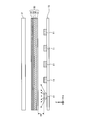
- FIG. 1 is a schematic layered structure diagram showing the main configuration of the display device of the embodiment.
- FIG. 2 is a schematic perspective view showing a case where the main configuration of the lighting device is viewed from the other surface side.
- FIG. 3 is an XY plan view showing the relationship between the light source and the light guide member.
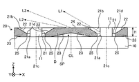
- FIG. 4 is a sectional view taken along line AA of FIG.
- FIG. 5 is an enlarged cross-sectional view showing the configuration within the range B of FIG.
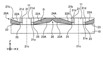
- FIG. 6 is an enlarged cross-sectional view showing a characteristic configuration of the first modification.
- FIG. 7 is an enlarged cross-sectional view showing a characteristic configuration of the second modification.
- FIG. 8 is an enlarged cross-sectional view showing a characteristic configuration of Modification 3.
- FIG. 1 is a schematic layered structure diagram showing the main configuration of the display device of the embodiment.
- FIG. 2 is a schematic perspective view showing a case where the main configuration of the lighting device is viewed from the other surface side.
- FIG. 9 is an enlarged cross-sectional view showing a characteristic configuration of Modification 4.
- FIG. 10 is an XY plan view showing the relationship between the light source and the light guide member of Modification 4.
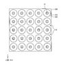
- FIG. 11 is an XY plan view showing the relationship between the light source and the light guide member of Modification 5.
- FIG. 12 is a diagram showing a configuration example in which mirror finishing is performed.
- FIG. 13 is a diagram showing a configuration example of the light guide member in which the second inclined surface 22 is omitted.
- FIG. 14 is a diagram showing a configuration example of a display device different from the present invention.
- FIG. 1 is a schematic layered structure diagram showing the main configuration of the display device 100 of the embodiment.
- the display device 100 includes a display panel P and a lighting device 1.
- the display panel P is a light transmissive type, and displays an image using light that is transmitted.
- the light L along the Z direction is schematically attached, but the light from the lighting device 1 is not limited to the light along the Z direction, as described later.
- the display panel P is illuminated from one surface (back surface P1) side and displays an image on the other surface (display surface P2) side.
- the display panel P is, for example, a transmissive liquid crystal display panel in which a plurality of pixels are arranged, but may be a semi-transmissive liquid crystal display panel or a transmissive display panel according to another method. Good.
- the illumination device 1 is provided on one surface side of the display panel P and illuminates the display panel P.
- the three directions orthogonal to each other are referred to as the X direction, the Y direction, and the Z direction.
- the lighting device 1 and the display panel P face each other in the Z direction.
- the display surface of the display panel P corresponds to the XY plane. It is also possible to adopt a configuration in which these three directions are not orthogonal to each other.
- FIG. 2 is a schematic perspective view showing a case where the main configuration of the lighting device 1 is viewed from the other surface side.
- FIG. 2 for the purpose of simply showing the positional relationship of the light guide member 20 with respect to other configurations such as the light source substrate 10 and the light source 11, a specific shape of the light guide member 20 described with reference to FIG. Is omitted.
- FIG. 2 for the purpose of more clearly showing the positional relationship between the light source 11 and the light guide member 20 when viewed from the other surface side, the configuration of the optical sheet 30 is illustrated with a part cut away.
- the lighting device 1 includes a light source substrate 10, a plurality of light sources 11, a light guide member 20, and an optical sheet 30.
- the light source substrate 10 is a substrate on which a plurality of light sources 11 are arranged, and has wirings connected to the light sources 11.
- the light source 11 is, for example, a light emitting element such as an LED, and emits light according to power supply.
- the power supply to the light source 11 is performed via the wiring of the light source substrate 10.
- An LED driving circuit (not shown) is connected to the light source substrate 10. More specifically, a terminal is formed on the bottom surface of the light source 11, and the terminal is connected to the wiring of the light source substrate 10.
- Each light source 11 can be individually turned on/off under the control of the drive circuit. In addition, the brightness when turned on can be adjusted individually.
- the plurality of light sources 11 are arranged in a matrix in the X and Y directions along the XY plane.
- FIG. 2 shows an example in which 5 ⁇ 5 light sources 11 arranged in the X direction and 5 arranged in the Y direction are arranged in a matrix, the number and arrangement of the light sources 11 are arbitrary.
- the arrangement of the plurality of light sources 11 is not limited to the matrix shape described above, and various arrangements are possible, including a staggered arrangement, a radial arrangement, and an arrangement in which these parts are partially omitted.
- the light from the light source 11 is emitted radially, as schematically shown by the arrow from the light source 11 in FIG. More specifically, the light from the light source 11 is emitted not only from the upper surface of the light source 11 but also from the side surface. That is, most of the light from the light source 11 has not only the Z-direction component but also the X-direction and Y-direction components. Therefore, the light from the light source 11 is not limited to the Z direction and includes light in the direction along the XY plane.
- the light guide member 20 has a plurality of holes (through holes) 21 at predetermined intervals and a light guide portion D surrounding the hole 21.
- Each light source 11 is housed in the hole 21 by arranging the light guide member 20 so as to overlap the light source substrate 10.
- the light guide member 20 is a member formed using a translucent synthetic resin or glass, but if it is a translucent member that reflects or transmits light depending on the angle of the surface with respect to the light, a specific member is used.
- the material can be changed appropriately. That is, the refractive index, reflectance and light diffusivity of the light guide member 20 itself can be changed as appropriate.
- the light guide member 20 guides the light from the light source 11 to the display panel P side. The specific influence of the light guide member 20 on the light from the light source 11 will be described later.
- the optical sheet 30 diffuses the light emitted from the light source 11.
- the optical sheet 30 shown in FIG. 2 has a configuration in which four optical sheets 31, 32, 33, and 34 having different optical characteristics are laminated, but the optical sheet 30 is not limited to this, and is a single-layer optical sheet. It may be an optical sheet having a laminated structure of two layers, three layers, or five or more layers.
- FIG. 3 is an XY plan view showing the relationship between the light source 11 and the light guide member 20.
- FIG. 4 is a sectional view taken along line AA of FIG.
- the light guide member 20 includes a plurality of holes 21 provided at predetermined intervals and a light guide portion D provided around the plurality of holes 21.
- the light guide section D has a second inclined surface 22, a first inclined surface 23, and a facing surface 24. Further, the second inclined surface 22 constitutes a part of the wall surface of the hole 21.
- the light guide member 20 is made of a light-transmissive plate material, the plane including the facing surface 24 may be referred to as an emission surface and the plane including the surface in contact with the light source substrate 10 may be referred to as a back surface.
- FIG. 5 is a cross-sectional view showing an enlarged configuration within a range B of FIG.
- the hole 21 is a hole penetrating from the surface (back surface) of the light guide member 20 on the light source substrate 10 side to the surface (emission surface) on the display panel P side.
- the light emitted from the light source 11 in the Z direction passes through the optical sheet 30 and illuminates the display panel P.
- the hole 21 has a first opening 21a on the back surface side and a second opening 21b on the emission surface side, and each of them has a rectangular XY plane shape.
- the light source 11 has a rectangular shape in the XY plane and a dimension in the X and Y directions of 1 [mm].
- the dimension of the first opening 21a in the X and Y directions is 1.6 [mm].
- the light source 11 is arranged in the center of the hole 21 from the XY plane viewpoint, but it is not essential that the center is exactly in the center.
- the light source 11 may be arranged inside the hole 21. Note that the above numerical values are examples and can be changed as appropriate.
- the light guide member 20 has a light guide structure that is provided with the hole 21 that is opened in the first direction (Z direction) and in which the light source 11 is arranged.
- the second inclined surface 22 is provided on the exit surface side of the light guide member 20.
- the second inclined surface 22 is inclined with respect to the Z direction and the XY plane.
- the second inclined surface 22 is a hole extending in a direction away from the center line 21c of the hole with the midway portion 21d of the hole 21 as a base end and continuously extending from the midway portion 21d toward the emission surface. It is the inner wall surface of 21. Due to the second inclined surface 22, a part of the light emitted from the light source 11 is emitted without being affected by at least one of reflection and refraction by the light guide member 20, that is, without passing through the light guide member 20.
- the midway portion 21d serving as the base end portion of the second inclined surface 22 is preferably provided on the back side with respect to the center of the light guide member 20 in the thickness direction. Further, the midway portion 21d is preferably on the back side of the emission surface of the light source 11 housed in the hole 21, and more preferably on the back side of half the height of the light source 11 from the light source substrate 10.
- the first inclined surface 23 is provided on the back surface side of the light guide member 20.
- the first inclined surface 23 is inclined with respect to the Z direction and the XY plane. Specifically, the first inclined surface 23 is spaced apart from the center line 21c of the hole 21 with the opening edge 25 of the first opening 21a of the hole 21 as a base end, and as it goes from the opening edge 25 toward the emission surface. Extend in the direction.
- the inclination of the first inclined surface 23 with the opening edge 25 as the base end is continuous from the light source 11 to the farthest end CL in any direction along the XY plane.
- the position of the terminal end CL is located on, for example, an intermediate line that is equidistant from the center lines 21c of the two adjacent holes 21.
- the light guide member 20 has a light guide structure in which the first inclined surface 23 that is inclined with respect to the Z direction and the XY plane is formed.
- the arrangement pitch of the light sources 11 in the X direction and the Y direction is 6 [mm].
- the pitch of the holes 21 of the light guide member 20 is also 6 mm. Therefore, the distance in the X direction (Y direction) from the center of a certain hole 21 to the terminal end CL is 3 [mm], but this is an example and can be changed as appropriate.
- the structure of the light guide member 20 is symmetrical between the two light sources 11 adjacent to each other with the terminal end CL interposed therebetween.
- the light L2, L3 that has entered the inner peripheral surface of the hole 21 along the XY plane, more specifically, the light emitted from the light source 11 is more than the Z-direction component.
- a part of the light having a large XY component or a component including a negative component in the Z direction is refracted from the second inclined surface 22 toward the inside of the light guide member 20, and is incident on the first inclined surface 23. Head to the side.
- the lights L2 and L3 are reflected toward the display panel P side by the first inclined surface 23, and travel toward the display panel P side at a position farther from the light source than the emission angle from the light source 11.
- the first inclined surface 23 and the second inclined surface 22 have different inclination angles with respect to the XY plane.
- the first inclined surface 23 has a steeper angle of inclination with respect to the XY plane than the second inclined surface 22.
- the inclination angle of the first inclined surface 23, the inclination angle of the second inclined surface 22, and the position of the starting point are set so that the light emitted from the light source 11 along the XY plane is closer to the display panel P side. It is desirable that it be adjusted so that it can be easily aimed at.
- the facing surface 24 is provided on the exit surface side of the light guide section D.
- the facing surface 24 faces the optical sheet along the XY plane.
- the facing surface 24 is a surface from which the light passing through the inside of the light guide portion D is emitted, as indicated by the lights L2 and L3 in FIG. Due to the refraction generated at the facing surface 24, the emission angles of the lights L2 and L3 are slightly increased.
- the surfaces of the light source 11 and the light guide member 20 facing the optical sheet 30 are located on the same plane along the XY plane.
- the thickness H of the light guide member 20 corresponds to the height of the light source 11 with respect to the light source substrate 10. It can also be said that the upper surface of the light source 11 and the emission surface of the light guide member 20 are coincident with each other. Therefore, the position of the facing surface 24 in the Z direction with respect to the light source substrate 10 is the same position as the upper surface of the light source 11 with the light source substrate 10 as the bottom. It is also possible to adopt a configuration in which the upper surface of the light source 11 and the emitting surface of the light guide member 20 are not on the same plane.
- the upper surface of the light source 11 is closer to the light source substrate 10 than the emission surface of the light guide member 20.
- the upper surface (crown) of the light source 11 is located inside the hole 21.
- the thickness H of the light guide member 20 is 0.8 [mm], but this is an example and can be changed as appropriate.
- the lights L2 and L3 are reflected by the first inclined surface 23 in the light guide portion D, so that the light source 11 emits light.
- Light can be more efficiently directed to the display panel P side.
- the lights L2 and L3 the light passes through the inside of the light guide member 20 rather than from the vicinity of the light source 11, thereby diffusing the light from the light source 11 to a position further away from the XY plane viewpoint. be able to. As a result, it is possible to reduce luminance unevenness in the XY plane viewpoint due to the distance from the light source 11.
- the light guide D is provided around the light source 11. As a result, the light guide member 20 is suppressed to a thickness H corresponding to the thickness of the light source 11. More specifically, the light guide portion D is not provided immediately above and around the light source 11, and the light from the light source 11 whose light component in the Z direction is larger than the light component in the X direction or the Y direction is guided. The light is emitted to the display panel P side without passing through the light section D. Therefore, the thickness H of the light guide member 20 is suppressed to about the thickness of the light source 11, and the thinner light source device 1 and thus the thinner display device 100 are provided.
- the light guide member 20 in order to diffuse the light from the light source 11, that is, to sufficiently reduce the brightness unevenness between the light sources, the light source 11 and the optical sheet 30 are used. It is necessary to provide a large gap ap for the diffusion of light (for example, a size equal to or larger than the height of the light source 11), and the gap ap makes it more difficult to reduce the thickness of the display device.
- the interval ap can be made smaller (for example, equal to or smaller than the height of the light source 11) as compared with the case where the light guide member 20 is not provided as shown in FIG. 1. Therefore, the thinner display device 100 can be provided.
- interval ap may be 0 or a value exceeding 0, but can be set to 1 [mm] or less in consideration of the pitch of the light source 11 of the embodiment.
- FIG. 6 is an enlarged cross-sectional view showing a characteristic configuration of the first modification.
- FIG. 6 and FIGS. 7 to 9 to be described later are enlarged cross-sectional views showing the configuration within the range B of FIG. 4 in the description of the embodiment.
- the inclined surface provided on the back side of the light guide member 20A includes a plurality of inclinations (inclination 23A, groove 26) having different positions with respect to the light source 11 and angles with respect to the XY plane.
- the light guide member 20A of Modification 1 is a groove provided at an intermediate position between the slope 23A provided in place of the first sloped surface 23 of the embodiment and the slopes 23A adjacent to each other in the direction in which the holes 21 are arranged. 26 and.
- the inclination 23A and the groove 26 have different inclination angles with respect to the XY plane.
- the groove 26 is provided behind the facing surface 24A at a larger angle with respect to the XY plane than the inclination 23A. As a result, more light can be emitted from the facing surface 24A.
- the inclination 23A shown in FIG. 6 and FIGS. 7 to 9 described later has a smaller inclination angle with respect to the XY plane than the first inclined surface 23, but this is an example and the present invention is not limited to this.
- the inclination angle of the inclination 23A with respect to the XY plane may be the same as that of the first inclined surface 23, or may be larger than that of the first inclined surface 23.
- an inclination 22A shown in FIG. 6 and FIGS. 7 to 9 described later is provided in place of the second inclined surface 22 of the embodiment.
- the inclination 22A has a smaller inclination angle with respect to the XY plane than the second inclined surface 22, but this is an example and the present invention is not limited to this.
- the inclination angle of the inclination 22A with respect to the XY plane may be the same as that of the second inclination surface 22, or may be larger than that of the second inclination surface 22.
- the width of the facing surface 24A shown in FIG. 6 and FIGS. 7 to 9 to be described later is smaller than the width of the facing surface 24 in the X direction, but this is an example and the present invention is not limited to this.
- the width of the facing surface 24A depends on the angle of inclination of the inclination 22A with respect to the XY plane.
- the groove 26 has a larger angle with the XY plane than the inclination 22A.
- FIG. 7 is an enlarged cross-sectional view showing a characteristic configuration of the second modification.
- Modification 2 Difference from the modified example 1 described with reference to FIG. 6 will be described, and the same components will be denoted by the same reference numerals and omitted.
- the emission surface side of the light guide member includes a plurality of inclinations having different positions with respect to the light source 11 and angles with respect to the XY plane.
- the light guide member 20B of Modification 2 has a groove 27 on the facing surface 24B in addition to the slope 22A.
- the groove 27 has an inclined surface that approaches the first inclined surface 23 from the facing surface 24B as it approaches the terminal end CL from the side closer to the hole 21.
- the inclination 22A and the groove 27 have different angles with respect to the XY plane.
- FIG. 8 is an enlarged cross-sectional view showing a characteristic configuration of Modification 3.
- 20 C of light guide members of the modification 3 have several groove
- the depth of each groove 28 is shallower than that of the groove 27, but may be the same or deeper. It is also possible to adopt a configuration in which the depth of each groove 28 becomes deeper from the outermost side toward the inner side.
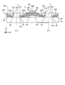
- FIG. 9 is an enlarged cross-sectional view showing a characteristic configuration of Modification 4.
- the light guide member 20D of Modification 4 has, in addition to the inclination 22A, a plurality of protrusions 29 that protrude from the facing surface 24D toward the display panel P side.
- FIG. 10 is an XY plan view showing the relationship between the light source 11 and the light guide member 20D of Modification 4.
- the protruding portion 29 is provided along the Y direction on the facing surface 24D between the plurality of light sources 11 arranged in the X direction. A plurality of such protrusions 29 are provided for each facing surface 24D.
- the plurality of protrusions 29 along the Y direction are arranged in the X direction.
- the protruding portion 29 is provided along the X direction on the facing surface 24D between the plurality of light sources 11 arranged in the Y direction.
- a plurality of such protrusions 29 are provided for each facing surface 24D.
- the plurality of protrusions 29 along the X direction are arranged in the Y direction.
- each protrusion 29 is an isosceles triangle with the display panel P side as the apex, as shown in FIG.
- the angle of the inclined surface of the protruding portion 29 with respect to the XY direction is larger than the inclinations 22A and 23A. Thereby, the emitted light from the facing surface 24D can be increased.
- a covering member 40 is provided at a position where the plurality of protrusions 29 along the X direction and the plurality of protrusions 29 along the Y direction intersect.
- the covering member 40 is adhesively fixed to the display panel P side of the light guide member 20D so as to cover the top of the protrusion 29 on the display panel P side.
- the covering member 40 is, for example, a cover made of a colorless resin having a light-transmitting property, but the cover member 40 is not limited to this, and a specific material can be appropriately changed.
- the optical sheet 30 is laminated on the display panel P side of the light guide member 20D provided with the covering member 40. As a result, it is possible to prevent the optical characteristics of the optical sheet 31 from being affected by the physical contact of the protrusions 29.
- the number of grooves 28 shown in FIG. 8 and the protrusion 29 shown in FIG. 9 is 6, which is formed between two adjacent light sources 11. However, this is only an example and the number is not limited to this. It is possible. Further, the angles, sizes, and numbers of the grooves 28 and the protrusions 29 can be changed appropriately.
- FIG. 11 is an XY plan view showing the relationship between the light source 11 and the light guide member 20E of the fifth modification.
- the first opening 21a and the second opening 21b of the hole 21 are each formed in a circular shape.
- each inclined surface is formed in a mortar shape.
- FIG. 12 is a diagram showing a configuration example in which mirror finishing is performed.
- the light source substrate 10 side of the first inclined surface 23 (or the inclination 23A and the groove 26) may be mirror-finished to more reliably reflect light to the display panel P side.
- the mirror-finished portion 23M is further provided on the side of the first inclined surface 23 of the configuration shown in FIG. 5 on the light source substrate 10 side.
- a configuration similar to that of the mirror-finished portion 23M may be provided.
- the mirror-finished portion 23M is formed by forming a thin film of a compound such as a metal, an alloy, or an oxide by a processing treatment such as vapor deposition so that the thin film functions as a mirror surface.
- the forming method is not limited to this, and can be appropriately changed.
- a mirror sheet may be attached.
- FIG. 13 is a diagram showing a configuration example of the light guide member 20 in which the second inclined surface 22 is omitted.
- the second inclined surface 22 described with reference to FIG. 5 and the like is not essential.
- a configuration in which the second inclined surface 22 is omitted from the light guide member 20 of FIG. 5 may be adopted.
Landscapes
- Physics & Mathematics (AREA)
- General Physics & Mathematics (AREA)
- Optics & Photonics (AREA)
- Nonlinear Science (AREA)
- Engineering & Computer Science (AREA)
- Microelectronics & Electronic Packaging (AREA)
- Mathematical Physics (AREA)
- Chemical & Material Sciences (AREA)
- Crystallography & Structural Chemistry (AREA)
- General Engineering & Computer Science (AREA)
- Planar Illumination Modules (AREA)
- Liquid Crystal (AREA)
Abstract
表示装置は、一面側からの光の一部又は全部を他面側に透過させる表示パネルと、表示パネルの一面側に設けられる照明装置と、を備え、照明装置は、光を発する光源と、透光性を有し、表示パネルと対向する第1方向の配置が光源の配置に対応する導光部材とを備え、導光部材は、第1方向に開口して光源が内側に配置される孔と、孔の周囲を囲う導光部とを有し、導光部の一面側には、第1方向及び第1方向に直交する平面に対して傾斜する第1傾斜面が形成されている。
Description
本発明は、表示装置、照明装置、導光部材及び導光構造に関する。
複数の点状光源を所定の間隔で配置して、表示パネルを背面側から照明する構成が知られている(例えば特許文献1)。
発光ダイオード(LED:light emitting diode)のような点状光源を採用すると、LEDが直下に位置する箇所の輝度が相対的に最も明るく、LED同士の間隔に対応する箇所の輝度が相対的に暗くなる。
本発明は、上記の課題に鑑みてなされたもので、光源からの距離による輝度低下を低減できる表示装置、照明装置、導光部材及び導光構造を提供することを目的とする。
本発明の一態様による表示装置は、一面側からの光の一部又は全部を他面側に透過させる表示パネルと、前記表示パネルの前記一面側に設けられる照明装置と、を備え、前記照明装置は、光を発する光源と、透光性を有し、前記表示パネルと対向する第1方向の配置が前記光源の配置に対応する導光部材とを備え、前記導光部材は、前記第1方向に開口して前記光源が内側に配置される孔と、前記孔の周囲を囲う導光部とを有し、前記導光部の一面側には、前記第1方向及び前記第1方向に直交する平面に対して傾斜する第1傾斜面が形成されている。
本発明の一態様による照明装置は、一面側からの光の一部又は全部を他面側に透過させる表示パネルの前記一面側に設けられる照明装置であって、光源と、透光性を有し、前記表示パネルと対向する第1方向の配置が前記光源の配置に対応する導光部材とを備え、前記導光部材は、前記第1方向に開口して前記光源が内側に配置される孔と、前記孔の周囲を囲う導光部とを有し、前記導光部の一面側には、前記第1方向及び前記第1方向に直交する平面に対して傾斜する第1傾斜面が形成されている。
本発明の一態様による導光部材は、一面側からの光の一部又は全部を他面側に透過させる表示パネルの前記一面側に設けられる照明装置が有する光源が配置され、前記表示パネルと対向する第1方向に開口している孔と、透光性を有し、前記孔の周囲を囲う導光部とを有し、前記導光部の一面側には、前記第1方向及び前記第1方向に直交する平面に対して傾斜する第1傾斜面が形成されている。
本発明の一態様による導光構造は、第1方向に開口して内側に光源が配置される孔の周囲を囲う透光性の導光部の一面側に前記第1方向及び前記第1方向に直交する平面に対して傾斜する第1傾斜面が形成されている。
以下に、本発明の各実施の形態について、図面を参照しつつ説明する。なお、開示はあくまで一例にすぎず、当業者において、発明の主旨を保っての適宜変更について容易に想到し得るものについては、当然に本発明の範囲に含有されるものである。また、図面は説明をより明確にするため、実際の態様に比べ、各部の幅、厚さ、形状等について模式的に表される場合があるが、あくまで一例であって、本発明の解釈を限定するものではない。また、本明細書と各図において、既出の図に関して前述したものと同様の要素には、同一の符号を付して、詳細な説明を適宜省略することがある。
図1は、実施形態の表示装置100が備える主要構成を示す模式的な積層構造図である。表示装置100は、表示パネルPと、照明装置1とを備える。表示パネルPは、光透過型であり、透過する光を用いて画像を表示する。図1では、模式的にZ方向に沿う光に符号Lを付しているが、後述するように、照明装置1からの光はZ方向に沿う光に限らない。
具体的には、表示パネルPは、一面(背面P1)側から照明されて他面(表示面P2)側に画像を表示する。表示パネルPは、例えば複数の画素が配置された透過型の液晶表示パネルであるが、半透過型の液晶表示パネルであってもよいし、他の方式による透過型の表示パネルであってもよい。照明装置1は、表示パネルPの一面側に設けられて表示パネルPを照明する。以下の説明では、互いに直交する3方向をX方向、Y方向及びZ方向とする。照明装置1と表示パネルPはZ方向で対向している。また、表示パネルPの表示面はX-Y平面に相当する。なお、これら3方向は互いに直交していない構成を採用することも可能である。
図2は、照明装置1の主要構成を他面側から見た場合を示す模式的な斜視図である。図2では、光源基板10、光源11等の他の構成に対する導光部材20の位置関係を簡便に示す目的で、後述する図3等を参照して説明する導光部材20の具体的な形状に関する描写を省略している。また、図2では、他面側から見た光源11と導光部材20との位置関係をより明確に示す目的で、光学シート30の構成を一部切り欠いた状態で図示している。
図1及び図2に示すように、照明装置1は、光源基板10と、複数の光源11と、導光部材20と、光学シート30とを備える。光源基板10は、複数の光源11が配置される基板であり、光源11に接続される配線等を有する。
光源11は、例えばLEDのような発光素子であり、電力供給に応じて光を発する。光源11に対する電力供給は、光源基板10の配線を介して行われる。光源基板10には図示しないLEDの駆動回路が接続される。より具体的には、光源11の底面に端子が形成され、当該端子が光源基板10の配線に接続されている。各光源11は、当該駆動回路の制御下で個別に点灯/消灯が可能となっている。また、点灯時の明るさも個別に調整可能となっている。
図2に示すように、複数の光源11は、X-Y平面に沿ってX方向及びY方向にマトリクス状に配置される。図2では、X方向に5つ並び、Y方向に5つ並ぶ5×5の光源11がマトリクス状に配置されている例を示しているが、光源11の数及び配置は任意である。なお、複数の光源11の配置は、上記マトリクス状に限らず、千鳥状配置や放射状配置、及びこれらを一部欠落させた配置を含め様々な配置が可能である。
なお、図1の光源11からの矢印で模式的に示すように、光源11からの光は、放射状に照射される。より具体的には、光源11からの光は、光源11の上面からのみならず、側面からも出射される。すなわち、光源11からの光の多くはZ方向の成分のみならず、X方向及びY方向の成分を有している。従って、光源11からの光は、Z方向に限らず、X-Y平面に沿う方向の光も含む。
導光部材20は、所定の間隔で複数の孔(貫通孔)21と、孔21の周囲を囲う導光部Dとを有する。導光部材20を光源基板10に重ねて配置することにより、各光源11が孔21に収容される。
導光部材20は、透光性を有する合成樹脂又はガラスを用いて形成された部材であるが、光に対する面の角度によって光を反射又は透過させる透光性の部材であれば、具体的な素材については適宜変更可能である。すなわち、導光部材20自体の屈折率、反射率や光拡散性は、適宜変更可能である。導光部材20は、光源11からの光を表示パネルP側に誘導する。導光部材20が光源11からの光に与える具体的な影響については後述する。
光学シート30は、光源11から発せられた光を拡散させる。図2に示す光学シート30は、それぞれ光学特性が異なる4つの光学シート31,32,33,34が積層された構成であるが、これに限られるものでなく、単層の光学シートであってもよいし、2層、3層又は5層以上の積層構造を有する光学シートであってもよい。
図3は、光源11と導光部材20との関係を示すX-Y平面図である。図4は、図3のA-A断面図である。導光部材20は、所定の間隔で設けられる複数の孔21と、これら複数の孔21の周囲に設けられる導光部Dとを備えている。導光部Dは、第2傾斜面22、第1傾斜面23、対向面24を有する。また、第2傾斜面22は孔21の壁面の一部を構成する。なお、導光部材20は透光性の板材からなるが、対向面24を含む平面を出射面、光源基板10と接触する面を含む平面を背面と称することがある。
図5は、図4の範囲B内の構成を拡大して示す断面図である。孔21は、導光部材20の光源基板10側の面(背面)から表示パネルP側の面(出射面)まで貫通する孔である。光源11からのZ方向に出射される光は、光学シート30を通過して表示パネルPを照明する。
より具体的には、孔21は、背面側の第1開口21a及び出射面側の第2開口21bを有し、いずれもX-Y平面の形状が矩形状である。また、実施形態では、光源11は、X-Y平面の形状が矩形状であってX方向及びY方向の寸法が1[mm]である。これに対し、第1開口21aのX方向及びY方向の寸法が1.6[mm]である。理想的には、光源11は、X-Y平面視点で孔21の中央に配置されるが、厳密に中央であることは必須でない。光源11は、孔21の内側に配置されていればよい。なお、上記数値は例示であって、適宜変更可能である。このように、導光部材20は、第1方向(Z方向)に開口して内側に光源11が配置される孔21が設けられた導光構造を有する。
第2傾斜面22は、導光部材20の出射面側に設けられる。第2傾斜面22は、Z方向及びX-Y平面に対して傾斜する。具体的には、第2傾斜面22は、孔21の中途部21dを基端として、当該中途部21dから連続して出射面に向かうにつれて孔の中心線21cから離間する方向に延在する孔21の内壁面である。第2傾斜面22によって、光源11から発せられる光の一部は、導光部材20による反射及び屈折の少なくとも一方の影響を受けることなく、即ち、導光部材20を介することなく出射される。これらの光はZ方向の成分が多く含まれており、導光部材20による誘導を必要とすることなく十分な輝度で表示パネルPに向けて出射される。なお、第2傾斜面22の基端部となる上記中途部21dは、導光部材20の厚さ方向中心よりも背面側に設けられることが好ましい。また、当該中途部21dは、孔21に収容された光源11の出射面よりも背面側が好ましく、光源11の光源基板10からの高さの半分よりも背面側に設けられることがより好ましい。
第1傾斜面23は、導光部材20の背面側に設けられる。第1傾斜面23は、Z方向及びX-Y平面に対して傾斜する。具体的には、第1傾斜面23は、孔21の第1開口21aの開口縁25を基端として、当該開口縁25から連続して出射面に向かうにつれて孔21の中心線21cから離間する方向に延在する。開口縁25を基端とした第1傾斜面23の傾斜は、X-Y平面に沿う任意の方向において光源11から最も遠い終端CLまで連続する。終端CLの位置は、例えば、隣り合う2つの孔21の中心線21cから等距離となる中間線上に位置する。隣り合う2つの孔21の間には、上記中間線を境に対称的に連続する2つの第1傾斜面23を屋根部とした空間SPが形成される。このように、導光部材20は、Z方向及びX-Y平面に対して傾斜する第1傾斜面23が形成された導光構造を有する。
なお、実施形態では、X方向及びY方向の光源11の配置ピッチは6[mm]である。導光部材20の孔21のピッチも6mmである。従って、ある孔21の中心から終端CLまでのX方向(Y方向)の距離は3[mm]であるが、これは一例であって適宜変更可能である。
図5に示すように、導光部材20の構造は、終端CLを挟んで隣り合う2つの光源11の間で対称である。
図5に示すように、孔21の内周面に対してX-Y平面に沿って進入した光L2、L3より具体的には、光源11から出射される光のうち、Z方向成分よりもX-Y成分が大きいもの、或いは、Z方向のマイナスの成分を含む光の一部は、第2傾斜面22から導光部材20の内部に向かって屈折して入射し、第1傾斜面23側に向かう。そしてこれら光L2、L3は、第1傾斜面23によって表示パネルP側に反射されることで、光源11からの出射角度に比して光源から遠方となる位置で表示パネルP側に向かう。なお、第1傾斜面23と第2傾斜面22は、X-Y平面に対する傾斜角度が異なる。第1傾斜面23は、第2傾斜面22よりもX-Y平面に対する傾斜角度が急角度である。
なお、第1傾斜面23の傾斜角度、第2傾斜面22の傾斜角度、起点の位置は、光源11から発せられる光のうちX-Y平面に沿って射出される光をより表示パネルP側に向けやすくなるよう調整されることが望ましい。
対向面24は、導光部Dの出射面側に設けられる。対向面24は、X-Y平面に沿い、光学シートと対向する。対向面24は、図5の光L2,L3が示すように、導光部D内部を通過する光が出射する面である。対向面24で生じる屈折によって光L2,L3の出射角度が若干大きくなる。
実施形態では、光源11と導光部材20は、光学シート30と対向する面がX-Y平面に沿う同一平面上に位置する。具体的には、図5に示すように、導光部材20の厚さHは、光源基板10に対する光源11の高さに対応する。また、光源11の上面と導光部材20の出射面とが一致しているともいえる。このため、光源基板10に対する対向面24のZ方向の位置は、光源基板10を底部とした光源11の上面と同じ位置である。なお、これら光源11の上面と導光部材20の出射面とが同一平面上にない構成も採用することができる。例えば、導光部材20の出射面よりも光源11の上面の方が光源基板10に近い位置である構成を採用することができる。この場合、当該光源11の上面(頭頂部)は孔21内に位置することになる。
なお、実施形態では、導光部材20の厚みHが0.8[mm]であるが、これは一例であって適宜変更可能である。
以上、実施形態によれば、図5を参照して説明した光L2,L3のように、導光部D内の第1傾斜面23でこれらの光L2,L3が反射することによって光源11からの光をより効率的に表示パネルP側に向かわせることができる。また、光L2,L3のように、光源11の近傍からではなく、導光部材20の内部を光が通過することで、光源11からX-Y平面視点でより離れた位置に光を拡散させることができる。これにより、光源11からの距離によるX-Y平面視点での輝度ムラを低減できる。
また、図5を参照して説明した光L1のように、第2傾斜面22によって、光路中に導光部Dが介在しないことによって、反射を伴わなくても表示パネルP側に向かう光をそのまま表示パネルP側に向かわせることができる。
また、導光部Dは光源11の周囲に設けられている。これによって導光部材20は光源11の厚さ相当の厚みHに抑えられている。より具体的には、光源11の直上及びその周囲には導光部Dが設けられず、光源11からの光のうち、Z方向の成分がX方向やY方向の成分よりも大きい光は導光部Dを介することなく表示パネルP側に出射される。このため、導光部材20の厚みHが光源11の厚み程度に抑えられ、より薄型の光源装置1、ひいてはより薄型の表示装置100が提供される。
仮に、導光部材20がない場合、図14に示すように、光源11からの光を拡散させるために、すなわち、光源間の輝度ムラを十分に低減するためには、光源11と光学シート30との間に光の拡散のための間隔apを大きく(例えば光源11の高さ以上となる大きさ)設ける必要があり、当該間隔apによって表示装置全体の厚みが増すことによって薄型化をより困難にする。これに対し、実施形態によれば、図1に示すように導光部材20がない場合に比して間隔apをより小さく(例えば光源11の高さと同じかそれ以下の大きさ)することができ、より薄型の表示装置100を提供できる。
なお、間隔apは、0であってもよいし、0を超える値であってもよいが、実施形態の光源11のピッチを考慮しても1[mm]以下にすることができる。
(変形例)
以下、図6から図11を参照して、実施形態の変形例について説明する。変形例の説明では、実施形態と同様の構成に同じ符号を付して説明を省略する。
以下、図6から図11を参照して、実施形態の変形例について説明する。変形例の説明では、実施形態と同様の構成に同じ符号を付して説明を省略する。
(変形例1)
図6は、変形例1が有する特徴的な構成を拡大して示す断面図である。図6及び後述する図7から図9は、実施形態の説明における図4の範囲B内の構成を拡大して示す断面図である。
図6は、変形例1が有する特徴的な構成を拡大して示す断面図である。図6及び後述する図7から図9は、実施形態の説明における図4の範囲B内の構成を拡大して示す断面図である。
変形例1において導光部材20Aの背面側に設けられる傾斜面は、光源11に対する位置及びX-Y平面に対する角度がそれぞれ異なる複数の傾斜(傾斜23A、溝26)を含む。具体的には、変形例1の導光部材20Aは、実施形態の第1傾斜面23に代えて設けられる傾斜23Aと、孔21が並ぶ方向に隣り合う傾斜23A同士の中間位置に設けられる溝26とを含む。傾斜23Aと溝26とは、X-Y平面に対する傾斜の角度が異なる。図6に示す例では、溝26は、傾斜23AよりもX-Y平面に対して大きい角度を有して対向面24Aの背後に設けられている。これによって、より多くの光を対向面24Aから出射することができる。
図6及び後述する図7から図9に示す傾斜23Aは、第1傾斜面23に比してX-Y平面に対する傾斜の角度が小さいが、これは一例であってこれに限られるものでない。傾斜23Aは、X-Y平面に対する傾斜の角度が第1傾斜面23と同様であってもよいし、第1傾斜面23よりも大きい角度であってもよい。
また、図6及び後述する図7から図9に示す傾斜22Aは、実施形態の第2傾斜面22に代えて設けられる。傾斜22Aは、第2傾斜面22に比してX-Y平面に対する傾斜の角度が小さいが、これは一例であってこれに限られるものでない。傾斜22Aは、X-Y平面に対する傾斜の角度が第2傾斜面22と同様であってもよいし、第2傾斜面22よりも大きい角度であってもよい。これに伴い、図6及び後述する図7から図9に示す対向面24Aは、X方向の幅が対向面24よりも小さくなっているが、これは一例であってこれに限られるものでない。対向面24Aの幅は、X-Y平面に対する傾斜22Aの傾斜の角度に応じる。なお、溝26は、傾斜22AよりもX-Y平面に対して大きい角度を有している。
(変形例2)
図7は、変形例2が有する特徴的な構成を拡大して示す断面図である。変形例2以降の変形例については、図6を参照して説明した変形例1との差異について説明し、同様の構成について同じ符号を付して省略する。
図7は、変形例2が有する特徴的な構成を拡大して示す断面図である。変形例2以降の変形例については、図6を参照して説明した変形例1との差異について説明し、同様の構成について同じ符号を付して省略する。
変形例2及び後述する変形例3,4では、導光部材の出射面側には、傾斜22Aに加えて、光源11に対する位置及びX-Y平面に対する角度が異なる複数の傾斜を含む。具体的には、変形例2の導光部材20Bは、傾斜22Aに加えて、対向面24Bに溝27を有する。
溝27は、孔21に近い側から終端CLに近づくに従って対向面24Bから第1傾斜面23に近づく傾斜面を有する。このように、傾斜22Aと溝27とは、X-Y平面に対する角度がそれぞれ異なる。
(変形例3)
図8は、変形例3が有する特徴的な構成を拡大して示す断面図である。変形例3の導光部材20Cは、傾斜22Aに加えて、対向面24Cに複数の溝28を有する。各溝28の深さは、溝27よりも浅いが、同じであってもよいし、より深くてもよい。また、各溝28の深さは、最外側から内側に向かうにしたがって深くなる構成を採用することも可能である。
図8は、変形例3が有する特徴的な構成を拡大して示す断面図である。変形例3の導光部材20Cは、傾斜22Aに加えて、対向面24Cに複数の溝28を有する。各溝28の深さは、溝27よりも浅いが、同じであってもよいし、より深くてもよい。また、各溝28の深さは、最外側から内側に向かうにしたがって深くなる構成を採用することも可能である。
(変形例4)
図9は、変形例4が有する特徴的な構成を拡大して示す断面図である。変形例4の導光部材20Dは、傾斜22Aに加えて、対向面24Dから表示パネルP側に突出する複数の突出部29を有する。
図9は、変形例4が有する特徴的な構成を拡大して示す断面図である。変形例4の導光部材20Dは、傾斜22Aに加えて、対向面24Dから表示パネルP側に突出する複数の突出部29を有する。
図10は、光源11と変形例4の導光部材20Dとの関係を示すX-Y平面図である。突出部29は、X方向に並ぶ複数の光源11間の対向面24DにおいてY方向に沿うよう設けられる。係る突出部29は、対向面24D毎に複数設けられる。Y方向に沿う複数の突出部29は、X方向に並ぶ。また、突出部29は、Y方向に並ぶ複数の光源11間の対向面24DにおいてX方向に沿うよう設けられる。係る突出部29は、対向面24D毎に複数設けられる。X方向に沿う複数の突出部29は、Y方向に並ぶ。
各突出部29の断面形状は、図9に示すように、表示パネルP側を頂点とする二等辺三角形状である。突出部29の傾斜面のX-Y方向に対する角度は、傾斜22A、23Aよりも大きい。これにより、対向面24Dからの出射光を増大させることができる。
また、X方向に沿う複数の突出部29とY方向に沿う複数の突出部29とが交差する位置には、被覆部材40が設けられる。被覆部材40は、突出部29の表示パネルP側の頭頂部を覆うよう、導光部材20Dの表示パネルP側に接着固定される。被覆部材40は、例えば、透光性を有する無色の樹脂製のカバーであるが、これに限られるものでなく、具体的な素材については適宜変更可能である。
変形例4では、光学シート30は、被覆部材40が設けられた導光部材20Dの表示パネルP側に積層される。これによって、突出部29の物理的接触によって光学シート31の光学特性が影響を受けることを抑制することができる。
図8に示す溝28及び図9に示す突出部29は、隣り合う2つの光源11間に形成される数が6であるが、これは一例であってこれに限られるものでなく、適宜変更可能である。また、これら溝28や突出部29の角度や大きさ、数は適宜変更可能である。
(変形例5)
図11は、光源11と変形例5の導光部材20Eとの関係を示すX-Y平面図である。本変形例では、孔21の第1開口21a及び第2開口21bがそれぞれ円状に形成されている。これに伴い、各傾斜面は、すり鉢状に形成される。
図11は、光源11と変形例5の導光部材20Eとの関係を示すX-Y平面図である。本変形例では、孔21の第1開口21a及び第2開口21bがそれぞれ円状に形成されている。これに伴い、各傾斜面は、すり鉢状に形成される。
図12は、鏡面加工が施された構成例を示す図である。第1傾斜面23(又は傾斜23A及び溝26)の光源基板10側には、表示パネルP側に光をより確実に反射する鏡面加工を施してもよい。図12では、図5に示す構成の第1傾斜面23の光源基板10側に鏡面加工部23Mをさらに設けているが、これに限られるものでなく、傾斜23A及び溝26の光源基板10側にも鏡面加工部23Mと同様の構成を設けてもよい。鏡面加工部23Mは、例えば蒸着等の加工処理によって金属、合金又は酸化物等の化合物による薄膜を形成して当該薄膜を鏡面として機能させるようにしたものであるが、鏡面加工部23Mの具体的な形成方法はこれに限られるものでなく適宜変更可能である。例えば、ミラーシートを貼り付けるようにしてもよい。
図13は、第2傾斜面22が省略された導光部材20の構成例を示す図である。図5等を参照して説明した第2傾斜面22は、必須でない。例えば図13に示すように、図5の導光部材20から第2傾斜面22を省略した構成を採用してもよい。
また、本実施形態において述べた態様によりもたらされる他の作用効果について本明細書記載から明らかなもの、又は当業者において適宜想到し得るものについては、当然に本発明によりもたらされるものと解される。
1 照明装置
10 光源基板
11 光源
20 導光部材
21 孔
22 第2傾斜面
23 第1傾斜面
24 対向面
25 底部
30,31,32,33,34 光学シート
40 被覆部材
100 表示装置
D 導光部
P 表示パネル
P1 背面
P2 表示面
10 光源基板
11 光源
20 導光部材
21 孔
22 第2傾斜面
23 第1傾斜面
24 対向面
25 底部
30,31,32,33,34 光学シート
40 被覆部材
100 表示装置
D 導光部
P 表示パネル
P1 背面
P2 表示面
Claims (10)
- 一面側からの光の一部又は全部を他面側に透過させる表示パネルと、
前記表示パネルの前記一面側に設けられる照明装置と、を備え、
前記照明装置は、
光を発する光源と、
透光性を有し、前記表示パネルと対向する第1方向の配置が前記光源の配置に対応する導光部材とを備え、
前記導光部材は、
前記第1方向に開口して前記光源が内側に配置される孔と、
前記孔の周囲を囲う導光部とを有し、
前記導光部の一面側には、前記第1方向及び前記第1方向に直交する平面に対して傾斜する第1傾斜面が形成されている
表示装置。 - 前記第1傾斜面は、前記光源に対する位置ならびに前記第1方向及び前記平面に対する角度がそれぞれ異なる複数の傾斜を含む
請求項1に記載の表示装置。 - 前記導光部の他面側には、前記第1方向及び前記平面に対して傾斜する第2傾斜面が形成されている
請求項1又は2に記載の表示装置。 - 前記第2傾斜面は、前記光源に対する位置ならびに前記第1方向及び前記平面に対する角度がそれぞれ異なる複数の傾斜を含む
請求項3に記載の表示装置。 - 前記第2傾斜面は、前記表示パネルと対向する前記光源の端部の位置に対して前記表示パネル側に突出する突出部を含む
請求項4に記載の表示装置。 - 前記突出部の前記表示パネル側に設けられる被覆部材を備える
請求項5に記載の表示装置。 - 前記光源と前記導光部は、前記表示パネルと対向する端部が前記平面に沿う同一平面上に位置する
請求項1から4のいずれか一項に記載の表示装置。 - 一面側からの光の一部又は全部を他面側に透過させる表示パネルの前記一面側に設けられる照明装置であって、
光源と、
透光性を有し、前記表示パネルと対向する第1方向の配置が前記光源の配置に対応する導光部材とを備え、
前記導光部材は、
前記第1方向に開口して前記光源が内側に配置される孔と、
前記孔の周囲を囲う導光部とを有し、
前記導光部の一面側には、前記第1方向及び前記第1方向に直交する平面に対して傾斜する第1傾斜面が形成されている
照明装置。 - 一面側からの光の一部又は全部を他面側に透過させる表示パネルの前記一面側に設けられる照明装置が有する光源が配置され、前記表示パネルと対向する第1方向に開口している孔と、
透光性を有し、前記孔の周囲を囲う導光部とを有し、
前記導光部の一面側には、前記第1方向及び前記第1方向に直交する平面に対して傾斜する第1傾斜面が形成されている
導光部材。 - 第1方向に開口して内側に光源が配置される孔の周囲を囲う透光性の導光部の一面側に前記第1方向及び前記第1方向に直交する平面に対して傾斜する第1傾斜面が形成されている
導光構造。
Priority Applications (3)
| Application Number | Priority Date | Filing Date | Title |
|---|---|---|---|
| CN201980086523.3A CN113260908B (zh) | 2018-12-27 | 2019-10-04 | 显示装置、照明装置、导光部件及导光构造 |
| US17/357,145 US11333818B2 (en) | 2018-12-27 | 2021-06-24 | Display device, illumination device, and light guiding member |
| US17/742,653 US11768325B2 (en) | 2018-12-27 | 2022-05-12 | Display device, illumination device, and light guiding member |
Applications Claiming Priority (2)
| Application Number | Priority Date | Filing Date | Title |
|---|---|---|---|
| JP2018245958A JP7197351B2 (ja) | 2018-12-27 | 2018-12-27 | 表示装置、照明装置、導光部材及び導光構造 |
| JP2018-245958 | 2018-12-27 |
Related Child Applications (1)
| Application Number | Title | Priority Date | Filing Date |
|---|---|---|---|
| US17/357,145 Continuation-In-Part US11333818B2 (en) | 2018-12-27 | 2021-06-24 | Display device, illumination device, and light guiding member |
Publications (1)
| Publication Number | Publication Date |
|---|---|
| WO2020137075A1 true WO2020137075A1 (ja) | 2020-07-02 |
Family
ID=71125754
Family Applications (1)
| Application Number | Title | Priority Date | Filing Date |
|---|---|---|---|
| PCT/JP2019/039399 Ceased WO2020137075A1 (ja) | 2018-12-27 | 2019-10-04 | 表示装置、照明装置、導光部材及び導光構造 |
Country Status (4)
| Country | Link |
|---|---|
| US (2) | US11333818B2 (ja) |
| JP (1) | JP7197351B2 (ja) |
| CN (1) | CN113260908B (ja) |
| WO (1) | WO2020137075A1 (ja) |
Cited By (1)
| Publication number | Priority date | Publication date | Assignee | Title |
|---|---|---|---|---|
| CN114879370A (zh) * | 2022-06-15 | 2022-08-09 | 业成科技(成都)有限公司 | 导光结构、图像生成单元及虚像显示装置 |
Families Citing this family (2)
| Publication number | Priority date | Publication date | Assignee | Title |
|---|---|---|---|---|
| JP7368750B2 (ja) * | 2021-07-29 | 2023-10-25 | 日亜化学工業株式会社 | 発光モジュールおよび面状光源 |
| JP2024040698A (ja) * | 2022-09-13 | 2024-03-26 | 日亜化学工業株式会社 | 発光モジュール |
Citations (4)
| Publication number | Priority date | Publication date | Assignee | Title |
|---|---|---|---|---|
| KR20060111997A (ko) * | 2005-04-26 | 2006-10-31 | 서울반도체 주식회사 | 백색 발광다이오드를 채택한 백라이트 패널 |
| JP2006302687A (ja) * | 2005-04-21 | 2006-11-02 | Fuji Photo Film Co Ltd | 導光板、これを備える面状照明装置および液晶表示装置 |
| JP2010080130A (ja) * | 2008-09-24 | 2010-04-08 | Toppan Printing Co Ltd | 面発光装置及び表示装置 |
| JP2016045995A (ja) * | 2014-08-20 | 2016-04-04 | 三菱電機株式会社 | 面光源装置および液晶表示装置 |
Family Cites Families (15)
| Publication number | Priority date | Publication date | Assignee | Title |
|---|---|---|---|---|
| US6811282B1 (en) * | 2003-04-18 | 2004-11-02 | Heng Huang Kuo | Straight down-type backlight module assembly structure |
| JP2005018997A (ja) * | 2003-06-23 | 2005-01-20 | Kawaguchiko Seimitsu Co Ltd | バックライト装置 |
| ES2367044T3 (es) * | 2005-08-24 | 2011-10-27 | Koninklijke Philips Electronics N.V. | Módulo de iluminación. |
| JP5033545B2 (ja) * | 2007-09-05 | 2012-09-26 | 株式会社日立製作所 | 映像表示装置 |
| JP2009081063A (ja) * | 2007-09-26 | 2009-04-16 | Toppan Printing Co Ltd | バックライトユニット及び液晶表示装置 |
| US20110037740A1 (en) * | 2008-12-15 | 2011-02-17 | Panasonic Corporation | Planar illumination device and liquid crystal display |
| KR101264323B1 (ko) * | 2011-05-30 | 2013-05-22 | 경북대학교 산학협력단 | 점광원을 이용한 면발광 백라이트 유닛 및 면발광 램프 |
| CN102829392A (zh) | 2012-07-26 | 2012-12-19 | 深圳市华星光电技术有限公司 | 背光模块及显示装置 |
| KR20150024959A (ko) * | 2013-08-27 | 2015-03-10 | 주식회사 루멘스 | 백라이트 유닛 |
| US10001592B2 (en) * | 2013-11-22 | 2018-06-19 | Lumens Co., Ltd. | Backlight unit, double cone-shaped reflector, double cone-shaped reflector strip, illumination apparatus, and method of manufacturing double cone-shaped reflector |
| DE102013226181B4 (de) * | 2013-12-17 | 2021-01-28 | Zumtobel Lighting Gmbh | Optisches Element, sowie Anordnung zur Lichtabgabe |
| JP6528503B2 (ja) | 2015-03-30 | 2019-06-12 | 大日本印刷株式会社 | Ledバックライト及びそれを用いたled表示装置 |
| CN105759500A (zh) * | 2016-03-16 | 2016-07-13 | 深圳Tcl新技术有限公司 | 量子点背光模组及液晶电视 |
| CN107505769B (zh) * | 2017-08-15 | 2021-02-26 | 京东方科技集团股份有限公司 | 背光结构和显示装置 |
| US11307455B2 (en) * | 2019-09-25 | 2022-04-19 | Nichia Corporation | Light-emitting module having array of light sources, some aligned and others offset with array of lense structures |
-
2018
- 2018-12-27 JP JP2018245958A patent/JP7197351B2/ja active Active
-
2019
- 2019-10-04 CN CN201980086523.3A patent/CN113260908B/zh active Active
- 2019-10-04 WO PCT/JP2019/039399 patent/WO2020137075A1/ja not_active Ceased
-
2021
- 2021-06-24 US US17/357,145 patent/US11333818B2/en active Active
-
2022
- 2022-05-12 US US17/742,653 patent/US11768325B2/en active Active
Patent Citations (4)
| Publication number | Priority date | Publication date | Assignee | Title |
|---|---|---|---|---|
| JP2006302687A (ja) * | 2005-04-21 | 2006-11-02 | Fuji Photo Film Co Ltd | 導光板、これを備える面状照明装置および液晶表示装置 |
| KR20060111997A (ko) * | 2005-04-26 | 2006-10-31 | 서울반도체 주식회사 | 백색 발광다이오드를 채택한 백라이트 패널 |
| JP2010080130A (ja) * | 2008-09-24 | 2010-04-08 | Toppan Printing Co Ltd | 面発光装置及び表示装置 |
| JP2016045995A (ja) * | 2014-08-20 | 2016-04-04 | 三菱電機株式会社 | 面光源装置および液晶表示装置 |
Cited By (2)
| Publication number | Priority date | Publication date | Assignee | Title |
|---|---|---|---|---|
| CN114879370A (zh) * | 2022-06-15 | 2022-08-09 | 业成科技(成都)有限公司 | 导光结构、图像生成单元及虚像显示装置 |
| CN114879370B (zh) * | 2022-06-15 | 2023-09-29 | 业成科技(成都)有限公司 | 导光结构、图像生成单元及虚像显示装置 |
Also Published As
| Publication number | Publication date |
|---|---|
| US11333818B2 (en) | 2022-05-17 |
| US11768325B2 (en) | 2023-09-26 |
| US20220268986A1 (en) | 2022-08-25 |
| JP7197351B2 (ja) | 2022-12-27 |
| CN113260908A (zh) | 2021-08-13 |
| US20210318483A1 (en) | 2021-10-14 |
| CN113260908B (zh) | 2024-10-01 |
| JP2020106690A (ja) | 2020-07-09 |
Similar Documents
| Publication | Publication Date | Title |
|---|---|---|
| KR101171546B1 (ko) | 측면 조광형 백라이트 장치 | |
| JP5085864B2 (ja) | バックライトシステム及びそれを採用した液晶表示装置 | |
| US9053650B2 (en) | Backlight unit and display apparatus thereof | |
| JP2009128647A (ja) | 液晶表示装置 | |
| KR20080091461A (ko) | 액정 표시 장치용 백 라이트 | |
| US11768325B2 (en) | Display device, illumination device, and light guiding member | |
| TWI470169B (zh) | 光源模組 | |
| KR20150117510A (ko) | 광학 부재, 및 이를 포함하는 백라이트 유닛 | |
| WO2017170017A1 (ja) | 照明装置及び表示装置 | |
| JP6490136B2 (ja) | 面状照明装置 | |
| JP6406220B2 (ja) | 面光源装置、表示装置及び、電子機器 | |
| CN108241236B (zh) | 背光单元及具有背光单元的显示装置 | |
| US20240231146A1 (en) | Light flux controlling member, light emitting device, surface light source device and display device | |
| KR20200133087A (ko) | 천공 반사부재를 갖는 백라이트 장치 | |
| CN102330925B (zh) | 背光模块 | |
| JP5078640B2 (ja) | 照明装置及びこれを用いた液晶表示装置 | |
| KR20090003758A (ko) | 도광판 및 이를 구비한 백라이트 유니트 및 이를 구비한액정 표시 장치 | |
| JP2017091931A (ja) | 面光源装置 | |
| KR102594391B1 (ko) | 백라이트 유닛 및 이를 포함하는 액정표시장치 | |
| KR20170078480A (ko) | 액정 표시 장치 | |
| JP2008258096A (ja) | 面光源装置 | |
| JP7360965B2 (ja) | カップホルダー | |
| JP2008103087A (ja) | 照明装置 | |
| KR20160049588A (ko) | 백라이트 장치 | |
| JP2025182904A (ja) | 光学シート、光学部材及び照明装置 |
Legal Events
| Date | Code | Title | Description |
|---|---|---|---|
| 121 | Ep: the epo has been informed by wipo that ep was designated in this application |
Ref document number: 19902586 Country of ref document: EP Kind code of ref document: A1 |
|
| NENP | Non-entry into the national phase |
Ref country code: DE |
|
| 122 | Ep: pct application non-entry in european phase |
Ref document number: 19902586 Country of ref document: EP Kind code of ref document: A1 |