WO2020130071A1 - プリント配線板の製造方法 - Google Patents
プリント配線板の製造方法 Download PDFInfo
- Publication number
- WO2020130071A1 WO2020130071A1 PCT/JP2019/049799 JP2019049799W WO2020130071A1 WO 2020130071 A1 WO2020130071 A1 WO 2020130071A1 JP 2019049799 W JP2019049799 W JP 2019049799W WO 2020130071 A1 WO2020130071 A1 WO 2020130071A1
- Authority
- WO
- WIPO (PCT)
- Prior art keywords
- layer
- copper plating
- copper
- plating layer
- forming
- Prior art date
- Legal status (The legal status is an assumption and is not a legal conclusion. Google has not performed a legal analysis and makes no representation as to the accuracy of the status listed.)
- Ceased
Links
Images

Classifications
-
- H—ELECTRICITY
- H05—ELECTRIC TECHNIQUES NOT OTHERWISE PROVIDED FOR
- H05K—PRINTED CIRCUITS; CASINGS OR CONSTRUCTIONAL DETAILS OF ELECTRIC APPARATUS; MANUFACTURE OF ASSEMBLAGES OF ELECTRICAL COMPONENTS
- H05K3/00—Apparatus or processes for manufacturing printed circuits
- H05K3/02—Apparatus or processes for manufacturing printed circuits in which the conductive material is applied to the surface of the insulating support and is thereafter removed from such areas of the surface which are not intended for current conducting or shielding
- H05K3/06—Apparatus or processes for manufacturing printed circuits in which the conductive material is applied to the surface of the insulating support and is thereafter removed from such areas of the surface which are not intended for current conducting or shielding the conductive material being removed chemically or electrolytically, e.g. by photo-etch process
-
- H—ELECTRICITY
- H05—ELECTRIC TECHNIQUES NOT OTHERWISE PROVIDED FOR
- H05K—PRINTED CIRCUITS; CASINGS OR CONSTRUCTIONAL DETAILS OF ELECTRIC APPARATUS; MANUFACTURE OF ASSEMBLAGES OF ELECTRICAL COMPONENTS
- H05K3/00—Apparatus or processes for manufacturing printed circuits
- H05K3/10—Apparatus or processes for manufacturing printed circuits in which conductive material is applied to the insulating support in such a manner as to form the desired conductive pattern
- H05K3/18—Apparatus or processes for manufacturing printed circuits in which conductive material is applied to the insulating support in such a manner as to form the desired conductive pattern using precipitation techniques to apply the conductive material
-
- H—ELECTRICITY
- H05—ELECTRIC TECHNIQUES NOT OTHERWISE PROVIDED FOR
- H05K—PRINTED CIRCUITS; CASINGS OR CONSTRUCTIONAL DETAILS OF ELECTRIC APPARATUS; MANUFACTURE OF ASSEMBLAGES OF ELECTRICAL COMPONENTS
- H05K3/00—Apparatus or processes for manufacturing printed circuits
- H05K3/22—Secondary treatment of printed circuits
- H05K3/26—Cleaning or polishing of the conductive pattern
Definitions
- the present invention relates to a method for manufacturing a printed wiring board.
- a copper clad laminate in which a copper foil is pasted on an insulating base material is used, and a resist pattern is formed on the copper foil, followed by chlorination.
- a circuit pattern is formed by a subtractive method of etching copper in a non-circuit portion with copper or iron chloride (for example, see Non-Patent Document 1).
- CCL copper clad laminate
- a printed wiring board can be suitably manufactured by patterning the formed conductive metal film by a subtractive method.
- the metal species of the metal particle layer and the metal plating layer are different, for example, when a copper plating layer is formed on the silver particle layer, portions other than the circuit pattern cannot be uniformly removed without residue by an etching solution, and the appearance There was a possibility of causing defects and deterioration of insulation reliability.
- the problem to be solved by the present invention is to form a silver particle layer as a plating underlayer specifically when a plating underlayer and a metal plating layer of different metal species are formed on an insulating substrate, It is an object of the present invention to provide a method for manufacturing a printed wiring board which is capable of uniformly removing a portion other than a circuit pattern without a residue even when a copper plating layer is formed on the layer, and which is excellent in appearance and insulation reliability.
- a silver particle layer is formed as a plating underlayer on an insulating substrate, and a copper plating layer is formed on the silver particle layer.
- a cleaning process with a specific chemical solution after the etching process by the subtractive method parts other than the circuit pattern can be removed uniformly without residue, and a printed wiring board with excellent appearance and insulation reliability can be manufactured. And completed the present invention.
- the present invention includes a step 1 of forming a silver particle layer (M1) containing silver particles on an insulating substrate (A), a copper plating layer formed on the silver particle layer (M1) by a plating method.
- the present invention provides a method for producing a printed wiring board, which comprises a step 3 of performing the above step and a step 4 of washing the laminate having the copper circuit pattern with a chemical solution.
- the present invention also includes a step 1′ of forming a silver particle layer (M1) containing silver particles after forming a primer layer (B) on an insulating substrate (A), the silver particle layer (M1). ), a step 2 of forming a copper plating layer (M2) by a plating method, a resist having a circuit pattern is formed on the copper plating layer (M2), and the copper plating layer (M2) in the non-circuit portion is removed by etching.
- the present invention provides a method for manufacturing a printed wiring board, comprising: a step 3 of producing a laminated body having a copper circuit pattern, and a step 4 of cleaning the laminated body having the copper circuit pattern with a chemical solution.
- the method for manufacturing a printed wiring board of the present invention By the method for manufacturing a printed wiring board of the present invention, a printed wiring board excellent in appearance and insulation reliability can be manufactured. Further, even if the base material has a smooth surface, sufficient adhesion can be secured, and a printed wiring board having a conductive metal layer having an arbitrary thickness can be manufactured. Furthermore, the method for producing a printed wiring board of the present invention is not limited to a flat base material, but can be applied to a three-dimensionally formed base material.
- the method for manufacturing a printed wiring board of the present invention can also be used for producing various electronic members having a patterned metal layer on the surface of a base material, such as a sensor, a connector, an electromagnetic wave shield, and an RFID. It can also be applied to the manufacture of antennas.
- the substrate having a metal pattern manufactured by the method for manufacturing a printed wiring board of the present invention is not only an electronic member but also a sliding member having a patterned metal layer on a substrate having various shapes and sizes. It can also be used as a functional part such as a part or as an article plated with decoration.
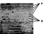
- FIG. 1 is a photograph showing the appearance of the printed wiring board prepared in Example 4 before cleaning.
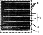
- FIG. 2 is a photograph showing the appearance of the printed wiring board prepared in Example 4 after being washed with a 5 mass% sodium thiosulfate aqueous solution.
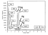
- FIG. 3 is a chart showing the results of elemental analysis of the non-cleaning region of the printed wiring board manufactured in Example 4.
- FIG. 4 is a chart showing elemental analysis results of a region in which the printed wiring board manufactured in Example 4 was washed with a 5 mass% sodium thiosulfate aqueous solution.
- the method for producing a printed wiring board of the present invention includes a step 1 of forming a silver particle layer (M1) containing silver particles, and a copper plating layer (M2) is formed on the silver particle layer (M1) by a plating method.
- Step 2 of forming a resist having a circuit pattern on the copper plating layer (M2), and removing the copper plating layer (M2) of the non-circuit portion by etching to produce a laminate having a copper circuit pattern; It has a step 4 of cleaning the laminate having the copper circuit pattern with a chemical solution.
- a more preferable aspect of the method for producing a printed wiring board of the present invention is that after forming the primer layer (B) on the insulating base material (A), the silver particle layer (M1) containing silver particles is formed.
- Step 1 ′ Step 2 of forming a copper plating layer (M 2) on the silver particle layer (M 1) by a plating method, Step 2 of forming a resist having a circuit pattern on the copper plating layer (M 2) Part of the copper plating layer (M2) is removed by etching to produce a laminate having a copper circuit pattern, and step 4 of cleaning the laminate having the copper circuit pattern with a chemical solution.
- Examples of the material of the insulating substrate (A) used in step 1 or step 1′ of the present invention include polyimide resin, polyamideimide resin, polyamide resin, polyethylene terephthalate resin, polybutylene terephthalate resin, polyethylene naphthalate resin, Polycarbonate resin, acrylonitrile-butadiene-styrene (ABS) resin, polyarylate resin, polyacetal resin, acrylic resin such as poly(meth)acrylate, polyvinylidene fluoride resin, polytetrafluoroethylene resin, polyvinyl chloride resin, polychlorination Vinylidene resin, vinyl chloride resin graft-copolymerized with acrylic resin, polyvinyl alcohol resin, polyethylene resin, polypropylene resin, urethane resin, cycloolefin resin, polystyrene, liquid crystal polymer (LCP), polyether ether ketone (PEEK) resin, polyphenylene Examples thereof include sulfide (PPS), poly
- thermosetting resin examples include epoxy resin, phenol resin, unsaturated imide resin, cyanate resin, isocyanate resin, benzoxazine resin, oxetane resin, amino resin, unsaturated polyester resin, allyl resin, dicyclopentadiene resin, Examples thereof include silicone resins, triazine resins, melamine resins and the like.
- examples of the inorganic filler include silica, alumina, talc, mica, aluminum hydroxide, magnesium hydroxide, calcium carbonate, aluminum borate, and borosilicate glass. These thermosetting resins and inorganic fillers may be used alone or in combination of two or more.
- the insulating base material (A) any of a flexible material, a rigid material and a rigid flexible material can be used. More specifically, a commercially available material formed into a film, a sheet or a plate may be used as the insulating base material (A), or may be selected from solutions, melts and dispersions of the various resins described above. You may use the material shape
- Step 1 of the method for producing a printed wiring board of the present invention is a step of forming a silver particle layer (M1) containing silver particles on the insulating base material (A).
- the silver particle layer (M1) serves as a plating underlayer when the copper plating layer (M2) is formed by a plating method in step 2 described later.
- Examples of the method of forming the silver particle layer (M1) include a method of coating a silver particle dispersion liquid on the insulating base material (A).
- the coating method of the silver particle dispersion is not particularly limited as long as the silver particle layer (M1) can be formed well, and various coating methods can be applied to the shape, size, and flexibility of the insulating base material (A) to be used. It may be appropriately selected depending on the degree.
- Specific coating methods include, for example, gravure method, offset method, flexographic method, pad printing method, gravure offset method, letterpress method, letterpress inversion method, screen method, microcontact method, reverse method, air doctor coater method, Blade coater method, air knife coater method, squeeze coater method, transfer roll coater method, kiss coater method, cast coater method, spray coater method, inkjet method, die coater method, spin coater method, bar coater method, dip coater method and the like can be mentioned. ..
- the method of applying the silver particle dispersion liquid on both surfaces of the film-shaped, sheet-shaped or plate-shaped insulating substrate (A) is not particularly limited as long as the silver particle layer (M1) can be well formed.
- the exemplified coating method may be appropriately selected.
- the silver particle layer (M1) may be simultaneously formed on both surfaces of the insulating base material (A), or may be formed on one surface of the insulating base material (A) and then on the other surface. You may.
- the coating method exemplified above may be appropriately selected according to the size and shape of the molded body, but a spray coater method, an inkjet method may be used. Method, dip coater method, etc. are suitable.
- the insulating base material (A) is coated with a silver particle dispersion liquid for the purpose of improving the coatability of the silver particle dispersion liquid and the adhesion of the copper plating layer (M2) formed in step 2 to the base material.
- Surface treatment may be performed before working.
- the surface treatment method for the insulating base material (A) is not particularly limited as long as the surface roughness becomes large and fine pitch pattern formability and signal transmission loss due to the rough surface do not pose a problem.
- the method may be appropriately selected. Examples of such a surface treatment method include UV treatment, vapor phase ozone treatment, liquid layer ozone treatment, corona treatment, and plasma treatment. These surface treatment methods can be carried out by one method or by combining two or more methods.
- the solvent contained in the silver particle dispersion liquid is volatilized by drying the coating film, and thus the insulating base material (A).
- the silver particles are fixed on top.
- the drying temperature and time may be appropriately selected according to the heat resistant temperature of the base material used, the selected step, the productivity, etc., and the temperature range is 20 to 350° C., and the time is about 1 to 200 minutes.
- the drying temperature is preferably in the range of 20 to 300° C. to enhance the electroless copper plating depositability. Therefore, the range of 20 to 250° C. is more preferable.
- the drying temperature is preferably in the range of 80 to 350°C, and preferably in the range of 100 to 300°C. More preferable.
- the insulating base material (A) having the silver particle layer (M1) formed thereon is subjected to a temperature range of 60 to 200° C. for 30 minutes to 2 weeks. Further, in the step 2 described later, when electrolytic copper plating is carried out, it is preferably carried out at a temperature range of 80 to 250° C. for 5 minutes to 1 hour.
- drying and aging or annealing may or may not be performed by blowing air. Further, the drying and aging or annealing may be performed in the atmosphere, under a substitution atmosphere of an inert gas such as nitrogen or argon, or under an air stream, or under vacuum.
- an inert gas such as nitrogen or argon
- the above-mentioned drying and aging or annealing are carried out by natural drying at the coating place. Alternatively, it can be performed in a dryer such as a blower or a constant temperature dryer.
- a dryer such as a blower or a constant temperature dryer.
- the insulating base material (A) is a roll film or a roll sheet, it is dried by continuously moving the roll material in the installed non-heating or heating space after the coating step. It can be performed.
- Examples of the heating method for drying at this time include a method using an oven, a hot air drying oven, an infrared drying oven, laser irradiation, microwaves, light irradiation (flash irradiation device), and the like. These heating methods may be used alone or in combination of two or more.
- the thickness of the silver particle layer (M1) is preferably in the range of 10 to 500 nm because it can be a more excellent plating underlayer in Step 2 described later.
- the thickness of the silver particle layer (M1) is preferably in the range of 10 to 500 nm, and in the range of 10 to 250 nm from the viewpoint of reducing the material cost. Is more preferable.
- the thickness of the silver particle layer (M1) is preferably in the range of 50 to 500 nm, and the conductivity for more efficiently performing electrolytic copper plating. From the viewpoints of securing the same and material cost, the range of 60 to 250 nm is more preferable.
- the silver particle layer (M1) preferably has high conductivity because the silver particles are in close contact with each other and joined when electrolytic copper plating is performed in step 2 described later. Further, the voids between the silver particles may be filled with plated copper by the plating method in step 2 described later. When the voids between the silver particles are filled with plated copper, the adhesion between the insulating base material (A) and the copper plating layer is improved.
- the silver particle dispersion liquid used for forming the silver particle layer (M1) is a dispersion of silver particles in a solvent.
- the shape of the silver particles is not particularly limited as long as it can form the silver particle layer (M1) well, and various shapes such as spherical shape, lens shape, polyhedral shape, flat plate shape, rod shape, and wire shape. Silver particles can be used. These silver particles may be used in one kind having a single shape, or may be used in combination of two or more kinds having different shapes.
- the average particle diameter is preferably in the range of 1 to 20,000 nm. Further, in the case of forming a fine metal pattern, since the homogeneity of the silver particle layer (M1) is further improved, the average particle diameter thereof is more preferably in the range of 1 to 200 nm, more preferably in the range of 1 to 50 nm. Are more preferred.
- the “average particle diameter” of the nanometer-sized particles is a volume average value measured by a dynamic light scattering method after diluting the silver particles with a good dispersion solvent. "Nanotrack UPA-150" manufactured by Microtrac can be used for this measurement.
- the minor axis thereof is preferably in the range of 1 to 200 nm, more preferably in the range of 2 to 100 nm, and further preferably 5 to 50 nm. Those in the range of are more preferable.
- the silver particle dispersion liquid used to form the silver particle layer (M1) is a dispersion of silver particles in various solvents, and the particle size distribution of the silver particles in the dispersion liquid is monodisperse. Alternatively, it may be a mixture of particles having an average particle diameter within the above range.
- An aqueous medium or an organic solvent can be used as a solvent for the dispersion liquid of the silver particles.
- the aqueous medium include distilled water, ion-exchanged water, pure water, and ultrapure water.
- the organic solvent include alcohol compounds, ether compounds, ester compounds and ketone compounds.
- Examples of the alcohol solvent or ether solvent include methanol, ethanol, n-propanol, isopropyl alcohol, n-butanol, isobutyl alcohol, sec-butanol, tert-butanol, heptanol, hexanol, octanol, nonanol, decanol, undecanol, dodecanol.
- Examples of the ketone solvent include acetone, cyclohexanone, methyl ethyl ketone and the like.
- Examples of the ester solvent include ethyl acetate, butyl acetate, 3-methoxybutyl acetate, 3-methoxy-3-methyl-butyl acetate and the like.
- a hydrocarbon solvent such as toluene, particularly a hydrocarbon solvent having 8 or more carbon atoms can be mentioned.
- hydrocarbon solvent having 8 or more carbon atoms examples include nonpolar solvents such as octane, nonane, decane, dodecane, tridecane, tetradecane, cyclooctane, xylene, mesitylene, ethylbenzene, dodecylbenzene, tetralin, and trimethylbenzenecyclohexane. And other solvents can be used in combination as required. Further, a mixed solvent such as mineral spirit and solvent naphtha may be used together.
- the solvent silver particles are stably dispersed, and the silver particle layer (on the insulating base material (A) or on the primer layer (B) formed on the insulating base material (A) described later, There is no particular limitation as long as M1) is well formed.
- the solvent may be used alone or in combination of two or more.
- the content of silver particles in the silver particle dispersion is adjusted so that the viscosity has optimum coating suitability according to the above-mentioned coating method, but a range of 0.5 to 90 mass% is preferable, The range of 1 to 60 mass% is more preferable, and the range of 2 to 10 mass% is further preferable.
- the silver particle dispersion liquid preferably maintains long-term dispersion stability without aggregation, fusion, or precipitation of the silver particles in the various solvent media, and the silver particles are dispersed in the various solvents. It is preferable to contain a dispersant for the purpose.
- a dispersant having a functional group that coordinates with silver particles is preferable, and examples thereof include a carboxyl group, an amino group, a cyano group, an acetoacetyl group, a phosphorus atom-containing group, a thiol group, a thiocyanato group, and glycinate.
- the dispersant include a functional group such as a group.
- the dispersant a commercially available or independently synthesized low molecular weight or high molecular weight dispersant can be used, and a solvent for dispersing silver particles or the insulating base material coated with a dispersion liquid of silver particles can be used.
- the type (A) or the like may be appropriately selected according to the purpose.
- a polycyclic hydrocarbon compound having a carboxyl group is preferably used.
- the adhesiveness between these two layers becomes good, so that the resin used for the primer layer (B) described below has It is preferable to use a compound having a reactive functional group [Y] capable of forming a bond with the reactive functional group [X].
- Examples of the compound having a reactive functional group [Y] include an amino group, an amide group, an alkylolamide group, a carboxyl group, an anhydrous carboxyl group, a carbonyl group, an acetoacetyl group, an epoxy group, an alicyclic epoxy group, an oxetane ring. , Compounds having a vinyl group, an allyl group, a (meth)acryloyl group, a (blocked) isocyanate group, a (alkoxy)silyl group and the like, a silsesquioxane compound and the like.
- the reactive functional group [Y] is preferably a basic nitrogen atom-containing group because the adhesion between the primer layer (B) and the silver particle layer (M1) can be further improved.
- the basic nitrogen atom-containing group include an imino group, a primary amino group, and a secondary amino group.
- the basic nitrogen atom-containing group may be present singly or plurally in one molecule of the dispersant. By containing a plurality of basic nitrogen atoms in the dispersant, some of the basic nitrogen atom-containing groups contribute to the dispersion stability of the silver particles by the interaction with the silver particles, and the remaining basic nitrogen atoms. The atom-containing group contributes to improving the adhesiveness with the insulating base material (A). Further, when a resin having a reactive functional group [X] is used for the primer layer (B) described below, the basic nitrogen atom-containing group in the dispersant may be present between the reactive functional group [X]. Is preferable, because the bond can be formed and the adhesion of the copper plating layer (M2) described later on the insulating base material (A) can be further improved.
- the dispersant is a dispersant from the viewpoint of stability of the dispersion liquid of silver particles, coatability, and forming a silver particle layer (M1) having good adhesion on the insulating base material (A).
- a polymer dispersant and as the polymer dispersant, polyalkyleneimine such as polyethyleneimine and polypropyleneimine, and a compound obtained by adding polyoxyalkylene to the polyalkyleneimine are preferable.
- the compound obtained by adding polyoxyalkylene to the polyalkyleneimine may be one in which polyethyleneimine and polyoxyalkylene are linearly bonded, and the side of the main chain composed of polyethyleneimine is It may be a chain grafted with polyoxyalkylene.
- Specific examples of the compound obtained by adding polyoxyalkylene to the polyalkyleneimine include, for example, a block copolymer of polyethyleneimine and polyoxyethylene, and ethylene oxide in a part of the imino group present in the main chain of polyethyleneimine. And a polyoxyethylene structure introduced into the polyoxyethylene structure, a polyalkyleneimine amino group, a polyoxyethylene glycol hydroxyl group, and an epoxy resin epoxy group are reacted.
- Examples of commercially available products of the polyalkyleneimine include “PAO2006W”, “PAO306”, “PAO318”, “PAO718” and the like of "Epomin (registered trademark) PAO series” manufactured by Nippon Shokubai Co., Ltd.
- the number average molecular weight of the polyalkyleneimine is preferably in the range of 3,000 to 30,000.
- the amount of the dispersant used to disperse the silver particles is preferably in the range of 0.01 to 50 parts by mass with respect to 100 parts by mass of the silver particles, and on the insulating base material (A).
- the silver particle layer (M1) exhibiting good adhesion can be formed on the primer layer (B) described below, the range of 0.1 to 10 parts by mass relative to 100 parts by mass of the silver particles is used.
- the range of 0.1 to 5 parts by mass is more preferable because the plating property and conductivity of the silver particle layer (M1) can be further improved.
- the method for producing the dispersion of silver particles is not particularly limited and may be produced by various methods.
- silver particles produced by a gas phase method such as evaporation in a low vacuum gas may be used as a solvent. You may disperse
- the solvent composition of the dispersion liquid at the time of production and the solvent composition of the dispersion liquid at the time of coating can be appropriately changed by solvent exchange or addition of a solvent, if necessary.
- the liquid phase method can be particularly preferably used because of the stability of the dispersion liquid and the ease of the manufacturing process.
- the liquid phase method can be produced, for example, by reducing metal ions in the presence of the polymer dispersant.
- the dispersion liquid of silver particles may further contain an organic compound such as a surfactant, a leveling agent, a viscosity adjusting agent, a film forming aid, an antifoaming agent and an antiseptic agent.
- an organic compound such as a surfactant, a leveling agent, a viscosity adjusting agent, a film forming aid, an antifoaming agent and an antiseptic agent.
- surfactant examples include nonionics such as polyoxyethylene nonylphenyl ether, polyoxyethylene lauryl ether, polyoxyethylene styryl phenyl ether, polyoxyethylene sorbitol tetraoleate, and polyoxyethylene/polyoxypropylene copolymer.
- fatty acid salts such as sodium oleate, alkyl sulfate ester salts, alkylbenzene sulfonates, alkylsulfosuccinates, naphthalene sulfonates, polyoxyethylene alkyl sulfates, sodium alkanesulfonate, sodium alkyldiphenyl ether sulfonate
- Anionic surfactants such as salts
- cationic surfactants such as alkylamine salts, alkyltrimethylammonium salts, and alkyldimethylbenzylammonium salts.
- leveling agent a general leveling agent can be used, and examples thereof include silicone compounds, acetylene diol compounds, and fluorine compounds.
- a general thickener can be used, for example, an acrylic polymer that can be thickened by adjusting to alkalinity, a synthetic rubber latex, and a thickening by the association of molecules.
- examples thereof include urethane resin, hydroxyethyl cellulose, carboxymethyl cellulose, methyl cellulose, polyvinyl alcohol, water-added castor oil, amide wax, polyethylene oxide, metal soap, dibenzylidene sorbitol and the like.
- a general film forming aid can be used, and examples thereof include anionic surfactants such as dioctyl sulfosuccinic acid ester soda salt, and hydrophobic nonionic surfactants such as sorbitan monooleate. , Polyether modified siloxane, silicone oil and the like.
- a general antifoaming agent can be used, and examples thereof include a silicone type antifoaming agent, a nonionic surfactant, a polyether, a higher alcohol, and a polymer type surfactant.
- preservative it is possible to use a general preservative, for example, isothiazoline preservatives, triazine preservatives, imidazole preservatives, pyridine preservatives, azole preservatives, pyrithione preservatives and the like. Are listed.
- the primer layer on the insulating base material (A) is formed before forming the silver particle layer (M1) containing silver particles on the insulating base material (A).
- the primer layer on the insulating base material (A) is formed before forming B.
- the primer layer there is a method of forming a silver particle layer (M1) containing silver particles on the layer (step 1′).
- the method of providing the primer layer (B) is preferable since the adhesion of the copper plating layer (M2) to the insulating base material (A) via the silver particle layer (M1) can be further improved.
- the primer layer (B) is obtained by applying a primer on a part or the whole surface of the insulating base material (A), and removing an aqueous medium, an organic solvent or the like contained in the primer. Can be formed.
- the primer is used for the purpose of improving the adhesion of the copper plating layer (M2) to the insulating base material (A), and various resins described below are dissolved or dispersed in a solvent. It is a liquid composition.
- the method for applying the primer to the insulating base material (A) is not particularly limited as long as the primer layer (B) can be well formed, and various applying methods can be used for the insulating base material (A).
- the shape may be appropriately selected depending on the shape, size, and degree of flexibility.
- Specific coating methods include, for example, gravure method, offset method, flexographic method, pad printing method, gravure offset method, letterpress method, letterpress inversion method, screen method, microcontact method, reverse method, air doctor coater method, Blade coater method, air knife coater method, squeeze coater method, transfer roll coater method, kiss coater method, cast coater method, spray coater method, inkjet method, die coater method, spin coater method, bar coater method, dip coater method and the like can be mentioned. ..
- the method of applying the primer to both surfaces of the film-, sheet-, or plate-shaped insulating base material (A) is not particularly limited as long as the primer layer (B) can be well formed, and the coating method illustrated above is used.
- the working method may be appropriately selected.
- the primer layer (B) may be simultaneously formed on both surfaces of the insulating base material (A), or may be formed on one surface of the insulating base material (A) and then on the other surface. May be.
- the coating method exemplified above may be appropriately selected according to the size and shape of the molded body, but a spray coater method, an inkjet method may be used. Method, dip coater method, etc. are suitable.
- the insulating base material (A) is surface-treated before the primer coating (step 1′) for the purpose of improving the coatability of the primer and the adhesion of the copper plating layer (M2) to the base material. You may go.
- the surface treatment method for the insulating base material (A) is the same as the surface treatment method for forming the silver particle layer (M1) containing silver particles on the insulating base material (A) described above. Can be formed.
- the method for forming the primer layer (B) by applying the primer on the surface of the insulating base material (A) and then removing the solvent contained in the applied layer for example, drying is performed using a dryer. Then, the method of volatilizing the solvent is generally used.
- the drying temperature may be set to a temperature within a range in which the solvent can be volatilized and does not adversely affect the insulating base material (A), and may be room temperature drying or heat drying.
- the specific drying temperature is preferably 20 to 350°C, more preferably 60 to 300°C.
- the drying time is preferably 1 to 200 minutes, more preferably 1 to 60 minutes.
- the above drying may be performed by blowing air or may not be performed in particular. Further, the drying may be performed in the air, in a substitution atmosphere of nitrogen, argon, or the like, or in an airflow, or may be performed in a vacuum.
- the insulating base material (A) is a sheet-shaped film, sheet, plate, or three-dimensional shaped body
- a dryer such as air blower or constant temperature dryer Can be done at.
- the insulating base material (A) is a roll film or a roll sheet, it is dried by continuously moving the roll material in the installed non-heating or heating space after the coating step. It can be performed.
- the film thickness of the primer layer (B) may be appropriately selected depending on the specifications and application of the molded product having a metal pattern produced by using the present invention, but the insulating base material (A) and the silver particle layer ( Since the adhesion with M1) can be further improved, the range of 10 nm to 30 ⁇ m is preferable, the range of 10 nm to 10 ⁇ m is more preferable, and the range of 10 nm to 5 ⁇ m is further preferable.
- the resin forming the primer layer (B) is a reactive functional group having reactivity with the reactive functional group [Y].
- a resin having [X] is preferable.
- the reactive functional group [X] include an amino group, an amide group, an alkylolamide group, a carboxyl group, an anhydrous carboxyl group, a carbonyl group, an acetoacetyl group, an epoxy group, an alicyclic epoxy group, an oxetane ring, and vinyl.
- a silsesquioxane compound can also be used as the compound forming the primer layer (B).
- the reactive functional group [Y] in the dispersant is a basic nitrogen atom-containing group
- the adhesion of the copper plating layer (M2) on the insulating base material (A) can be further improved.
- the resin forming the primer layer (B) has, as the reactive functional group [X], a carboxyl group, a carbonyl group, an acetoacetyl group, an epoxy group, an alicyclic epoxy group, an alkylolamide group, an isocyanate group, a vinyl group, Those having a (meth)acryloyl group and an allyl group are preferable.
- Examples of the resin forming the primer layer (B) include urethane resin, acrylic resin, core-shell type composite resin having urethane resin as a shell and acrylic resin as a core, epoxy resin, imide resin, amide resin, melamine resin. , A phenol resin, a urea-formaldehyde resin, a blocked isocyanate obtained by reacting a polyisocyanate with a blocking agent such as phenol, polyvinyl alcohol, polyvinyl pyrrolidone, and the like.
- the core-shell type composite resin having a urethane resin as a shell and an acrylic resin as a core can be obtained, for example, by polymerizing an acrylic monomer in the presence of the urethane resin. These resins may be used alone or in combination of two or more.
- a resin that produces a reducing compound by heating is preferable because the adhesion of the copper plating layer (M2) onto the insulating base material (A) can be further improved.
- the reducing compound include a phenol compound, an aromatic amine compound, a sulfur compound, a phosphoric acid compound, an aldehyde compound and the like.
- these reducing compounds a phenol compound and an aldehyde compound are preferable.
- a resin that produces a reducing compound by heating When a resin that produces a reducing compound by heating is used for the primer, it produces a reducing compound such as formaldehyde or phenol in the heating and drying process when forming the primer layer (B).
- the resin that produces a reducing compound by heating include, for example, a resin obtained by polymerizing a monomer containing N-alkylol(meth)acrylamide, and a urethane resin containing N-alkylol(meth)acrylamide as a shell.
- Core/shell type composite resin having a resin obtained by polymerizing monomers as a core, urea-formaldehyde-methanol condensate, urea-melamine-formaldehyde-methanol condensate, poly N-alkoxymethylol (meth)acrylamide, poly (meth)
- examples thereof include a formaldehyde adduct of acrylamide, a resin that forms formaldehyde by heating such as a melamine resin; and a resin that forms a phenol compound by heating such as a phenol resin and a phenol blocked isocyanate.
- a core-shell type composite resin having a urethane resin as a shell and a resin obtained by polymerizing a monomer containing N-alkylol (meth)acrylamide as a core, a melamine resin, and a phenol Blocked isocyanates are preferred.
- (meth)acrylamide means one or both of “methacrylamide” and “acrylamide”
- (meth)acrylic acid means “methacrylic acid” and “acrylic acid”. One or both.
- a resin that produces a reducing compound when heated is obtained by polymerizing a monomer having a functional group that produces a reducing compound when heated by a polymerization method such as radical polymerization, anionic polymerization, or cationic polymerization.
- Examples of the monomer having a functional group that produces a reducing compound upon heating include N-alkylol vinyl monomer, and specific examples thereof include N-methylol (meth)acrylamide and N-methoxymethyl ( (Meth)acrylamide, N-ethoxymethyl (meth)acrylamide, N-propoxymethyl (meth)acrylamide, N-isopropoxymethyl (meth)acrylamide, Nn-butoxymethyl (meth)acrylamide, N-isobutoxymethyl (meth ) Acrylamide, N-pentoxymethyl (meth)acrylamide, N-ethanol (meth)acrylamide, N-propanol (meth)acrylamide and the like.
- N-alkylol vinyl monomer examples thereof include N-methylol (meth)acrylamide and N-methoxymethyl ( (Meth)acrylamide, N-ethoxymethyl (meth)acrylamide, N-propoxymethyl (meth)acrylamide, N-isopropoxymethyl (meth)acrylamide, Nn-butoxy
- a uretdione bond is formed by self-reacting between isocyanate groups, or an isocyanate group and a functional group contained in another component are formed.
- the bond formed at this time may be formed before coating the silver particle dispersion liquid, or may not be formed before coating the silver particle dispersion liquid. It may be formed by heating after coating.
- blocked isocyanate those having a functional group formed by blocking an isocyanate group with a blocking agent can be mentioned.
- the blocked isocyanate preferably has the functional group in the range of 350 to 600 g/mol per 1 mol of the blocked isocyanate.
- the functional group preferably has 1 to 10 functional groups in one molecule of the blocked isocyanate, and more preferably has 2 to 5 functional groups.
- the number average molecular weight of the blocked isocyanate is preferably in the range of 1,500 to 5,000, more preferably in the range of 1,500 to 3,000, from the viewpoint of improving adhesion.
- the blocked isocyanate those having an aromatic ring are preferable from the viewpoint of further improving the adhesiveness.
- the aromatic ring include a phenyl group and a naphthyl group.
- the blocked isocyanate can be produced by reacting a part or all of the isocyanate groups of the isocyanate compound with a blocking agent.
- Examples of the isocyanate compound as a raw material of the blocked isocyanate include, for example, 4,4′-diphenylmethane diisocyanate, 2,4′-diphenylmethane diisocyanate, carbodiimide-modified diphenylmethane diisocyanate, crude diphenylmethane diisocyanate, phenylene diisocyanate, tolylene diisocyanate, and naphthalene diisocyanate.
- Polyisocyanate compound having an aromatic ring Aliphatic polyisocyanate compound such as hexamethylene diisocyanate, lysine diisocyanate, cyclohexane diisocyanate, isophorone diisocyanate, dicyclohexylmethane diisocyanate, xylylene diisocyanate, tetramethyl xylylene diisocyanate, or polyisocyanate having an alicyclic structure
- a compound etc. are mentioned.
- the burette body, the isocyanurate body, the adduct body, etc. of the above-mentioned polyisocyanate compound are also mentioned.
- examples of the above-mentioned isocyanate compound also include those obtained by reacting the polyisocyanate compound exemplified above with a compound having a hydroxyl group or an amino group.
- polyisocyanate compound having an aromatic ring When introducing an aromatic ring into the blocked isocyanate, it is preferable to use a polyisocyanate compound having an aromatic ring.
- polyisocyanate compounds having an aromatic ring 4,4'-diphenylmethane diisocyanate, tolylene diisocyanate, 4,4'-diphenylmethane diisocyanate isocyanurate, and tolylene diisocyanate isocyanurate are preferable.
- Examples of the blocking agent used for producing the blocked isocyanate include phenol compounds such as phenol and cresol; lactam compounds such as ⁇ -caprolactam, ⁇ -valerolactam and ⁇ -butyrolactam; formamide oxime, acetaldoxime, acetone oxime, Oxime compounds such as methyl ethyl ketoxime, methyl isobutyl ketoxime, cyclohexanone oxime; 2-hydroxypyridine, butyl cellosolve, propylene glycol monomethyl ether, benzyl alcohol, methanol, ethanol, n-butanol, isobutanol, dimethyl malonate, diethyl malonate, aceto Methyl acetate, ethyl acetoacetate, acetylacetone, butyl mercaptan, dodecyl mercaptan, acetanilide, acetic amide, succinimide, maleic imide, imid
- a blocking agent capable of generating an isocyanate group by dissociating by heating in the range of 70 to 200° C. is preferable, and a blocking agent capable of generating an isocyanate group dissociating by heating in the range of 110 to 180° C.
- Agents are more preferred.
- a phenol compound, a lactam compound, and an oxime compound are preferable, and a phenol compound is particularly preferable because it becomes a reducing compound when the blocking agent is eliminated by heating.
- Examples of the method for producing the blocked isocyanate include, for example, a method of mixing and reacting the previously produced isocyanate compound with the blocking agent, a method of mixing and reacting the blocking agent with raw materials used for producing the isocyanate compound, and the like. Are listed.
- the blocked isocyanate is produced by reacting the polyisocyanate compound with a compound having a hydroxyl group or an amino group to produce an isocyanate compound having an isocyanate group at a terminal, and then the isocyanate compound and the block. It can be produced by mixing and reacting with an agent.
- the content ratio of the blocked isocyanate obtained by the above method in the resin forming the primer layer (B) is preferably 50 to 100% by mass, more preferably 70 to 100% by mass.
- the melamine resin examples include mono- or polymethylol melamine obtained by adding 1 to 6 mol of formaldehyde to 1 mol of melamine; (poly)methylol melamine such as trimethoxymethylol melamine, tributoxymethylol melamine, and hexamethoxymethylol melamine. Ether compounds (the degree of etherification is arbitrary); urea-melamine-formaldehyde-methanol condensates and the like.
- a method of adding a reducing compound to a resin can also be mentioned.
- the reducing compound to be added include phenolic antioxidants, aromatic amine antioxidants, sulfur antioxidants, phosphoric acid antioxidants, vitamin C, vitamin E, ethylenediaminetetraacetic acid. Examples thereof include sodium, sulfite, hypophosphorous acid, hypophosphite, hydrazine, formaldehyde, sodium borohydride, dimethylamine borane and phenol.
- the method of adding a reducing compound to the resin is a resin that produces a reducing compound by heating, because the electrical properties may be reduced by the residual low molecular weight component or ionic compound in the end. Is more preferable.
- the primer used for forming the primer layer (B) preferably contains the resin in the range of 1 to 70% by mass from the viewpoint of coatability and film formability, and 1 to 20% by mass. What is contained in the range of% is more preferable.
- examples of the solvent usable for the primer include various organic solvents and aqueous media.
- examples of the organic solvent include toluene, ethyl acetate, methyl ethyl ketone, cyclohexanone, and the like
- examples of the aqueous medium include water, an organic solvent miscible with water, and a mixture thereof.
- water-miscible organic solvent examples include alcohol solvents such as methanol, ethanol, n-propanol, isopropanol, ethyl carbitol, ethyl cellosolve and butyl cellosolve; ketone solvents such as acetone and methyl ethyl ketone; ethylene glycol, diethylene glycol, propylene.
- alcohol solvents such as methanol, ethanol, n-propanol, isopropanol, ethyl carbitol, ethyl cellosolve and butyl cellosolve
- ketone solvents such as acetone and methyl ethyl ketone
- ethylene glycol diethylene glycol, propylene.
- alkylene glycol solvents such as glycols
- polyalkylene glycol solvents such as polyethylene glycol, polypropylene glycol and polytetramethylene glycol
- lactam solvents such as N-methyl-2
- the resin forming the primer layer (B) may have a functional group that contributes to the crosslinking reaction, such as an alkoxysilyl group, a silanol group, a hydroxyl group, an amino group, if necessary.
- the cross-linked structure formed by using these functional groups may have already formed the cross-linked structure before the step of forming the silver particle layer (M1) containing silver particles described later.
- a crosslinked structure may be formed after the step of forming the silver particle layer (M1) containing silver particles.
- the crosslinked structure is formed in the primer layer (B) before forming the copper plating layer (M2).
- a crosslinked structure may be formed in the primer layer (B) by, for example, aging after forming the copper plating layer (M2).
- a known agent such as a cross-linking agent, a pH adjusting agent, a film forming auxiliary agent, a leveling agent, a thickening agent, a water repellent, an antifoaming agent, etc. is appropriately added. You may use it.
- cross-linking agent examples include a metal chelate compound, a polyamine compound, an aziridine compound, a metal salt compound, and an isocyanate compound.
- a thermal cross-linking agent that reacts at a relatively low temperature of about 25 to 100° C. to form a cross-linking structure examples thereof include thermal crosslinking agents such as melamine-based compounds, epoxy-based compounds, oxazoline compounds, carbodiimide compounds, and blocked isocyanate compounds that react at a relatively high temperature of 100° C. or higher to form a crosslinked structure and various photocrosslinking agents.
- the amount of the cross-linking agent used varies depending on the type, but from the viewpoint of improving the adhesion of the copper plating layer (M2) onto the insulating base material (A), the total amount of the resin contained in the primer is 100 parts by mass.
- the range of 0.01 to 60 parts by mass is preferable, the range of 0.1 to 10 parts by mass is more preferable, and the range of 0.1 to 5 parts by mass is further preferable.
- a cross-linked structure may already be formed before the step of forming a silver particle layer (M1) containing silver particles in the subsequent step, and a silver particle layer containing silver particles.
- a crosslinked structure may be formed after the step of forming (M1).
- the crosslinked structure is formed in the primer layer (B) before forming the copper plating layer (M2).
- a crosslinked structure may be formed in the primer layer (B) by, for example, aging after forming the copper plating layer (M2).
- step 1′ of the present invention the method of forming the silver particle layer (M1) containing silver particles on the primer layer (B) is carried out by the method of forming silver particles containing silver particles on the insulating base material (A).
- the method is the same as the method for forming the particle layer (M1).
- the primer layer (B) improves the coatability of the silver particle dispersion liquid
- the copper plating layer (M2) is applied to the insulating base material (A) in the same manner as the insulating base material (A).
- surface treatment may be performed before coating the silver particle dispersion liquid.
- Examples of the plating method performed in step 2 include electrolytic copper plating, electroless copper plating, and a method combining electroless copper plating and electrolytic copper plating.
- electroless copper plating is performed as the plating method
- the silver particle layer (M1) is used as a catalyst seed.
- the copper plating layer (M2) may be formed as a thick film only by electroless copper plating, or electrolytic copper plating may be performed using the electroless copper plating layer formed by electroless copper plating as a conductive seed. By doing so, the copper plating layer (M2) may be thickened.
- the silver particle layer (M1) is used as a conductive seed.
- the copper plating layer (M2) may be formed by performing electrolytic copper plating after electroless copper plating. When electrolytic copper plating is used together, the plating deposition rate can be increased, which is advantageous because the production efficiency is increased.
- the thickness of the electroless copper plating layer may be appropriately selected as necessary.
- the range is preferably 0.1 ⁇ m to 2 ⁇ m, and from the viewpoint of improving productivity, the range is more preferably 0.15 ⁇ m to 1 ⁇ m. ..
- electrolytic copper plating may be carried out by using a known and commonly used method, but copper sulfate plating using a copper sulfate bath. Method is preferred.
- a pattern resist from which the resist in the non-circuit portion is removed is formed on the copper plating layer (M2).
- the method for forming the pattern resist is not particularly limited and may be a known method.
- a liquid photosensitive resist is applied onto the copper plating layer (M2) and dried, or a photosensitive dry film resist is used.
- the resist layer is formed by thermocompression bonding to the base material on which the copper plating layer (M2) is formed.
- the surface of the copper plating layer (M2) has a cleaning treatment with an acidic or alkaline chemical solution, a corona treatment, a plasma treatment, a UV treatment, a vapor phase ozone treatment, for the purpose of improving the adhesion to the resist layer.
- a cleaning treatment with an acidic or alkaline chemical solution, a corona treatment, a plasma treatment, a UV treatment, a vapor phase ozone treatment, for the purpose of improving the adhesion to the resist layer.
- Surface treatment such as liquid phase ozone treatment and treatment with a surface treatment agent may be performed. These surface treatments can be performed by one method or a combination of two or more methods.
- the treatment with the surface treatment agent for example, a treatment method using a rust preventive agent composed of a triazole compound, a silane coupling agent and an organic acid described in JP-A-7-258870, 2000-286546, a method of treating with an organic acid, a benzotriazole-based rust preventive and a silane coupling agent, and triazole, thiadiazole and the like described in JP-A-2002-363189.
- Japanese Patent Laid-Open No. 2005-214743 discloses a method of treating with a silane compound having a triazine ring and an amino group, and reacting a formylimidazole compound with an aminopropylsilane compound.
- Method using the imidazole silane compound thus obtained method using the azole silane compound described in JP-A-2016-134454, and one molecule described in JP-A-2017-203073
- a method of treating with a solution containing an aromatic compound having an amino group and an aromatic ring therein, a polybasic acid having two or more carboxyl groups, and a halide ion, and a triazole silane described in JP-A-2018-16865 A method of treating with a surface treatment agent containing a compound can be used.
- a photomask is passed through the resist layer formed on the copper plating layer (M2) or a circuit pattern is exposed with active light using a direct exposure machine.
- the exposure amount may be appropriately set as needed.
- the latent image formed on the resist layer by exposure is removed using a developing solution to form a patterned resist.
- the developer examples include aqueous solutions of sodium carbonate, potassium carbonate and the like.
- the exposed substrate is developed by immersing it in a developing solution or spraying the developing solution onto the resist by spraying or the like, and by this development, a pattern resist from which the circuit forming portion is removed can be formed. ..
- a descum treatment with plasma or a commercially available resist residue remover is used to create a footing at the boundary between the cured resist and the substrate or resist deposits remaining on the substrate surface.
- the resist residue such as may be removed.
- the resist used for forming the patterned resist in the present invention various commercially available resist materials can be used and may be appropriately selected depending on the desired pattern resolution, the type of exposure machine used, and the like.
- Examples of commercially available dry films include ALFO series manufactured by Nikko Materials Co., Sunfort series manufactured by Asahi Kasei Corporation, RD, RY, SL series, DL series manufactured by Hitachi Chemical Co., Ltd., and Liston manufactured by DuPont.
- a film, a PlateMaster series, or the like can be used.
- the copper plating layer (M2) in the non-circuit part is removed by etching.
- the copper plating layer (M2) can be removed using a known and commonly used etching solution generally used in the subtractive method, an etching solution containing cupric chloride or ferric chloride, or an alkaline etching solution. .. Among these, an etching solution containing cupric chloride or ferric chloride is preferable because it can suppress peeling of the resist pattern formed on the copper plating layer (M2) and form a circuit pattern as designed.
- a method of immersing a base material having a pattern resist formed on the copper plating layer (M2) in the etching solution examples thereof include a method in which an etching solution is sprayed on a base material having a pattern resist formed on the copper plating layer (M2).
- the temperature of the etching solution is preferably set in the temperature range of 40°C to 50°C. It is preferable to use a dedicated etching machine because the temperature of the etching solution can be easily set and the non-circuit portion can be efficiently removed by the effect of the shower pressure. In this way, a laminate having a circuit pattern can be obtained.
- the step 4 of the present invention is a step of cleaning the laminate having the circuit pattern obtained in the step 3 with a chemical solution for the purpose of removing the silver and silver compound residues remaining in the non-circuit part.
- a chemical solution that does not dissolve the copper plating layer (M2) of the circuit pattern portion is preferably used, and an aqueous solution containing a mixture of carboxylic acid and hydrogen peroxide can be preferably used. .. Regarding the mixing ratio of the mixture of the carboxylic acid and hydrogen peroxide, silver in the non-circuit portion can be preferentially dissolved, and the dissolution of the copper plating layer (M2) can be suppressed. Hydrogen peroxide is preferably in the range of 2 to 100 mol, and more preferably in the range of 2 to 50 mol.
- the mixture of carboxylic acid and hydrogen peroxide is preferably an aqueous solution diluted with water, and the content ratio of the mixture of carboxylic acid and hydrogen peroxide in the aqueous solution is preferably 2 to 65% by mass, The range of 2 to 30 mass% is more preferable.
- Step 3 when an etching solution containing cupric chloride or ferric chloride is used, a part of the silver particle layer (M1) may react with the etching solution to generate silver chloride. is there. In this case, the generated silver chloride remains as a residue in the non-circuit portion, which may cause a defective appearance of the printed wiring board and a decrease in insulation reliability between wirings.
- Step 4 is carried out.
- a chemical solution that dissolves silver chloride but does not dissolve the copper plating layer (M2) of the circuit pattern portion as the chemical solution used in the step 4.
- a chemical solution include an aqueous solution containing thiosulfate or tris(3-hydroxyalkyl)phosphine.
- Examples of the thiosulfate include ammonium thiosulfate, sodium thiosulfate, potassium thiosulfate and the like.
- Examples of the tris(3-hydroxyalkyl)phosphine include tris(3-hydroxymethyl)phosphine, tris(3-hydroxyethyl)phosphine, tris(3-hydroxypropyl)phosphine, and the like. These thiosulfates or tris(3-hydroxyalkyl)phosphines may be used alone or in combination of two or more.
- the cleaning with the chemical solution in the step 4 may be performed after the pattern formation by the etching treatment of the copper plating layer (M2) and the silver particle layer (M1) and before the resist is peeled off, or after the resist described below is peeled off. You can go.
- Examples of the cleaning method using the chemical solution in the step 4 include a method of immersing the laminate having the circuit pattern obtained in the step 3 in the chemical solution, and a method of spraying the chemical solution on the laminate with a spray or the like.
- the temperature of the chemical liquid can be used at room temperature (25° C.), but the temperature can be set to 30° C., for example, because the cleaning process can be stably performed without being affected by the outside air temperature.
- aqueous solution containing thiosulfate When used as the chemical liquid used in the step 4, its concentration may be appropriately set depending on the process time, the characteristics of the cleaning device used, etc., but is in the range of 0.1 to 40% by mass. Is preferable, and the range of 1 to 30% by mass is more preferable from the viewpoint of cleaning efficiency and stability of the chemical solution during continuous use.
- an aqueous solution containing the tris(3-hydroxyalkyl)phosphine is used as the chemical liquid used in the step 4, its concentration may be appropriately set depending on the process time, the characteristics of the cleaning apparatus used, etc.
- the range of 1 to 50% by mass is preferable, and the range of 1 to 40% by mass is more preferable from the viewpoint of cleaning efficiency and stability of the chemical solution during continuous use.
- the washing with the chemical solution in the step 4 may be performed by washing with an aqueous solution containing thiosulfate or tris(3-hydroxyalkyl)phosphine, and then washing with a mixture of the carboxylic acid and hydrogen peroxide. Good.
- step 4 it is preferable that after cleaning with a chemical solution, cleaning with water is performed to prevent the chemical solution used in step 4 and the components dissolved in the chemical solution from remaining on the printed wiring board to be manufactured.
- the water used for washing is not particularly limited, and tap water, distilled water, ion-exchanged water or the like may be used as necessary. Further, the washing may be performed not only once but a plurality of times. When performing a plurality of times, the types of water used for the first time and the second time and thereafter may be changed. As the water used in the first washing step, water having a pH adjusted by adding a trace amount of an acidic component or a basic component may be used.
- the removal of the resist of the circuit pattern formed in the above step 3 may be performed under the recommended conditions described in the catalog of the resist used, specifications, etc.
- As the resist stripping solution used for stripping the patterned resist a commercially available resist stripping solution or a 1.5 to 3 mass% aqueous solution of sodium hydroxide or potassium hydroxide set at 45 to 60° C. can be used. ..
- the resist can be peeled off by immersing the pattern-etched substrate in a peeling liquid or spraying the peeling liquid with a spray or the like.
- a printed wiring board excellent in appearance and insulation reliability can be manufactured. Further, even if the base material has a smooth surface, sufficient adhesion can be secured, and a printed wiring board having a conductive metal layer having an arbitrary thickness can be manufactured. Furthermore, the method for producing a printed wiring board of the present invention is not limited to a flat base material, but can be applied to a three-dimensionally formed base material.
- the method for producing a printed wiring board of the present invention can also be used for producing various electronic members having a patterned metal layer on the surface of a base material, such as a sensor, a connector, an electromagnetic wave shield, and an RFID. It can also be applied to the manufacture of antennas.
- the substrate having a metal pattern manufactured by the method for manufacturing a printed wiring board of the present invention is not only an electronic member but also a sliding member having a patterned metal layer on a substrate having various shapes and sizes. It can also be used as a functional part such as a part or as an article plated with decoration.
- Polyester polyol (polyester polyol obtained by reacting 1,4-cyclohexanedimethanol, neopentyl glycol, and adipic acid) in a nitrogen-substituted container equipped with a thermometer, a nitrogen gas introduction tube, and a stirrer 100 Parts by mass, 2,2-dimethylolpropionic acid 17.6 parts by mass, 1,4-cyclohexanedimethanol 21.7 parts by mass and dicyclohexylmethane-4,4'-diisocyanate 106.2 parts by mass, and methyl ethyl ketone 178 parts by mass.
- a urethane prepolymer solution having an isocyanate group at the terminal was obtained by reacting in a mixed solvent of.
- the chain dispersion of the urethane prepolymer was performed by adding 8.8 parts by mass of a 25% by mass aqueous ethylenediamine solution to the aqueous dispersion of the urethane prepolymer obtained above and stirring the mixture. Then, by aging and solvent removal, an aqueous dispersion of a urethane resin (nonvolatile content: 30% by mass) was obtained. The weight average molecular weight of the urethane resin was 53,000.
- a reaction vessel equipped with a stirrer, a reflux condenser, a nitrogen introduction tube, a thermometer, a dropping funnel for dropping the monomer mixture, and a dropping funnel for dropping the polymerization catalyst, 140 parts by mass of deionized water, and the urethane obtained above.
- 100 parts by mass of an aqueous resin dispersion was added, and the temperature was raised to 80° C. while blowing nitrogen.
- a monomer mixture consisting of 60 parts by weight of methyl methacrylate, 30 parts by weight of n-butyl acrylate and 10 parts by weight of Nn-butoxymethylacrylamide, and 20 parts by weight of 0.5% by weight aqueous ammonium persulfate solution. Parts and parts were added dropwise from separate dropping funnels over 120 minutes while maintaining the temperature inside the reaction container at 80°C.
- aqueous dispersion of a resin composition for a primer layer which is a core-shell type composite resin having a vinyl resin prepared from a raw material such as methyl methacrylate as a core layer. ..
- a vinyl monomer mixture consisting of 47.0 parts by mass of methyl methacrylate, 5.0 parts by mass of glycidyl methacrylate, 45.0 parts by mass of n-butyl acrylate, and 3.0 parts by mass of methacrylic acid in a reaction vessel under stirring.
- a surfactant (“Aqualon KH-1025” manufactured by Dai-ichi Kogyo Seiyaku Co., Ltd.: 25% by mass of active ingredient
- deionized water 5 parts by mass
- the remaining monomer pre-emulsion 114 parts by mass
- 30 parts by mass of an aqueous solution of potassium persulfate (1.0% by mass of the active ingredient) were separately added dropwise.
- a funnel was used to add dropwise over 180 minutes. After completion of dropping, the mixture was stirred at the same temperature for 60 minutes.
- Preparation Example 1 Preparation of silver particle dispersion liquid
- Silver particles and a dispersion are prepared by dispersing silver particles having an average particle size of 30 nm in a mixed solvent of 45 parts by mass of ethylene glycol and 55 parts by mass of ion-exchanged water using a compound of poly(ethylene)imine and polyoxyethylene added as a dispersant.
- a dispersion containing the agent was prepared.
- ion-exchanged water, ethanol and a surfactant were added to the obtained dispersion to prepare a 5% by mass silver particle dispersion liquid.
- Preparation Example 4 Preparation of chemical solution (4)
- 2.6 parts by mass of acetic acid was added to 47.4 parts by mass of water, and further 50 parts by mass of 35% by mass hydrogen peroxide solution was added to prepare a chemical solution (4).
- the chemical solution (4) had a molar ratio of hydrogen peroxide and carboxylic acid (hydrogen peroxide/carboxylic acid) of 13.6, and the content ratio of the mixture of hydrogen peroxide and carboxylic acid in the chemical solution (4) was 22. It was 0.4 mass %.
- Preparation Example 1 Preparation of polyphenylene sulfide (PPS) molded product
- the obtained polyphenylene sulfide resin composition was molded by an injection molding machine to prepare a PPS molded body having a size of 50 mm ⁇ 105 mm ⁇ 2 mm.
- Example 1 On the surface of a polyimide film (“Kapton 150EN-C” manufactured by Toray-Dupont Co., Ltd.; thickness: 38 ⁇ m), the silver particle dispersion liquid obtained in Preparation Example 1 was placed on a tabletop small coater (RK Print Coat Instrument Co., Ltd. K printing professor") was applied so that the average thickness after drying was 250 nm. Then, a silver particle layer was formed by drying and baking at 200° C. for 5 minutes using a hot air dryer.
- the silver particle layer formed above is immersed in an electroless copper plating solution ("OIC Copper” manufactured by Okuno Chemical Industries Co., Ltd., pH 12.5) at 45°C for 12 minutes to perform electroless copper plating, followed by electroless plating.
- An electroless copper plating solution ("OIC Copper” manufactured by Okuno Chemical Industries Co., Ltd., pH 12.5) at 45°C for 12 minutes to perform electroless copper plating, followed by electroless plating.
- a copper plating layer (film thickness 0.2 ⁇ m) was formed.
- the copper plating layer obtained by the electroless copper plating obtained above was set on the cathode side, the phosphorus-containing copper was set on the anode side, and the current density was 2.5 A/dm 2 using the electrolytic plating solution containing copper sulfate.
- the electrolytic plating solution 70 g/L of copper sulfate, 200 g/L of sulfuric acid, 50 mg/L of chloride ion, and 5 ml/L of additive (“Top Lucina SF-M” manufactured by Okuno Chemical Industries Co., Ltd.) were used.
- a combination of the copper plating layer formed by electroless copper plating and the copper plating layer formed by electrolytic copper plating formed thereon corresponds to the copper plating layer.
- the polyimide base material on which the pattern resist is formed on the copper plating layer is fixed to a polyethylene support plate with the base material facing upward, and is put into an etching device (small etching device ES-800 manufactured by Sun Hayato Co., Ltd.).
- the copper plating layer on the non-circuit part was removed by.
- a shower type etching was performed using a 38% by mass ferric chloride aqueous solution as the etching solution.
- the base material was discharged from the apparatus with the etching liquid remaining on the top. When the surface of the substrate was observed after washing with water and drying, a white residue was observed in the etched region.
- the above etched base material was dipped in the chemical solution (1) obtained in Preparation Example 10 for 10 seconds, further washed with water, and then the surface was observed. As a result, a white residue was removed.
- the film in which the copper plating layer of the non-circuit portion is etched is immersed in a 3% by mass aqueous solution of sodium hydroxide set at 50° C., and the pattern resist is peeled off to deposit copper on the polyimide film substrate.
- a printed wiring board on which a differential wiring pattern was formed was obtained.
- Example 1 A copper differential wiring pattern was formed on a polyimide film substrate in the same manner as in Example 1 except that cleaning with the chemical solution (1) was not performed. A white residue was observed in the etched non-circuit area, and elemental analysis of the surface confirmed that the white residue was silver chloride.
- Example 2 Similar to Example 1 except that the step of immersing in the chemical solution (1) for 10 seconds is performed not after the etching of the copper plating layer with the ferric chloride aqueous solution but after the pattern resist removing step using the sodium hydroxide aqueous solution. Then, a printed wiring board in which a copper differential wiring pattern was formed on a polyimide film substrate was obtained. Before the immersion in the chemical liquid (1) for 10 seconds, a white residue was observed in a part of the etching region, but after cleaning, no residue was observed.
- Example 2 A copper differential wiring pattern was formed on a polyimide film substrate in the same manner as in Example 2 except that cleaning with the chemical solution (1) was not performed. A white residue was observed in the etched non-circuit area, and elemental analysis of the surface confirmed that the white residue was silver chloride.
- Example 3 On the surface of a polyimide film (“Kapton 150EN-C” manufactured by Toray-DuPont Co., Ltd., thickness: 38 ⁇ m), the primer (B-1) obtained in Production Example 1 was placed on a small desk-top coater (RK Print Coat Instrument Co., Ltd.). "K printing professor” manufactured by Kogyo Co., Ltd.) was used for coating so that the thickness after drying would be 100 nm. Then, a primer layer was formed on the surface of the polyimide film by drying at 80° C. for 5 minutes using a hot air dryer.
- a primer layer was formed on the surface of the polyimide film by drying at 80° C. for 5 minutes using a hot air dryer.
- Example except that the base material coated with the silver particle dispersion liquid was changed from the polyimide film to the polyimide film coated with the primer (B-1), and the thickness of the silver particle layer was changed from 250 nm to 80 nm.
- a printed wiring board on which a copper differential wiring pattern was formed was obtained in the same manner as in 1.
- Example 4 A copper differential wiring pattern was formed in the same manner as in Example 2 except that the base material coated with the silver particle dispersion liquid was changed from the polyimide film to the polyimide film coated with the primer (B-1). The printed wiring board thus obtained was obtained.
- Example 5 A silver particle layer was formed in the same manner as in Example 1 except that the drying and baking time at 200° C. with a hot air dryer after coating the silver particle dispersion liquid was changed from 5 minutes to 30 minutes.
- the silver particle layer obtained above is set on the cathode side, phosphorus-containing copper is set on the anode side, and electrolytic plating is performed for 30 minutes at a current density of 2.5 A/dm 2 using an electrolytic plating solution containing copper sulfate.
- electrolytic plating is performed for 30 minutes at a current density of 2.5 A/dm 2 using an electrolytic plating solution containing copper sulfate.
- a copper plating layer film thickness 15 ⁇ m
- a silver nanoparticle layer and an electrolytic copper plating layer are formed on the polyimide film substrate.
- a laminated laminate was formed.
- Example 6 A silver particle layer was formed in the same manner as in Example 3 except that the drying and baking time at 200° C. with a hot air dryer after coating the silver particle dispersion liquid was changed from 5 minutes to 30 minutes. After forming the silver particle layer, a laminate in which a silver nanoparticle layer and an electrolytic copper plating layer were laminated on the polyimide film substrate was formed in the same manner as in Example 5.
- a printed wiring board in which a copper comb-teeth electrode pattern was formed on a polyimide film substrate was obtained in the same manner as in Example 2.
- a printed wiring board having a comb-teeth electrode pattern of copper formed on a polyimide film substrate was obtained in the same manner as in Example 4 except for the above.
- Example 8 A copper comb-teeth electrode pattern was formed on a polyimide film substrate in the same manner as in Example 7 except that the chemical solution used after pattern etching copper was changed to the chemical solution (2) or the chemical solution (3), respectively. I got a printed wiring board.
- a printed wiring board having a copper comb-teeth electrode pattern formed on a polyimide film substrate was obtained in the same manner as in Example 4 except that the change to (4) was performed.
- Example 3 A copper differential wiring pattern was formed on a polyimide film substrate in the same manner as in Example 10 except that cleaning with the chemical liquid (4) was not performed. Although no residue was visually observed in the etched non-circuit area, the presence of silver was confirmed by elemental analysis of the surface.
- Example 11 Using the PPS molded product obtained in Preparation Example 1 above, the primer (B-2) obtained in Production Example 2 was immersed for 10 seconds, the PPS molded product was lifted, and allowed to stand for 1 minute, and then dried with a hot air dryer. Was dried for 5 minutes at 200° C. to form a primer layer (thickness 130 nm) on the PPS molded product.
- the PPS molded product having the primer layer formed thereon was immersed in the silver particle dispersion liquid obtained in Preparation Example 1 for 10 seconds. After that, the PPS molded product was lifted up and allowed to stand for 1 minute, and then dried at 200° C. for 5 minutes using a hot air dryer to form a 100 nm thick silver particle layer on the primer layer. After forming a copper plating layer on the PPS substrate in the same manner as in Example 5, a dry film resist (“Liston FXR-20” manufactured by DuPont) was formed on the copper plating layer in the same manner as in Example 1. ]; resist film thickness 20 ⁇ m) was pressure-bonded at 100° C.
- Tables 1 and 2 summarize the evaluation results of the printed wiring boards obtained in Examples 1 to 13 and Comparative Examples 1 to 3.
- Circuit part Differential wiring pattern
- Non-circuit part b: Non-circuit part
- Cleaning area d: Non-cleaning area
Landscapes
- Engineering & Computer Science (AREA)
- Manufacturing & Machinery (AREA)
- Microelectronics & Electronic Packaging (AREA)
- Manufacturing Of Printed Wiring (AREA)
Abstract
本発明は、絶縁性基材(A)上に、銀粒子を含有する銀粒子層(M1)を形成する工程1、前記銀粒子層(M1)上に、めっき法によって、銅めっき層(M2)を形成する工程2、前記銅めっき層(M2)上に回路パターンのレジストを形成し、非回路部の銅めっき層(M2)をエッチング除去して銅回路パターンを有する積層体を作製する工程3、前記銅回路パターンを有する積層体を薬液で洗浄する工程4を有するプリント配線板の製造方法を提供する。当該製造方法は、絶縁性基材上に異なる金属種のめっき下地層と金属めっき層を形成した場合、具体的にはめっき下地層として銀粒子層を形成し、前記銀粒子層上に銅めっき層を形成した場合であっても、回路パターン以外の部分を残渣なく均一に除去でき、外観や絶縁信頼性に優れる。
Description
本発明は、プリント配線板の製造方法に関する。
従来、プリント配線板を製造する方法としては、絶縁性基材上に銅箔を貼り合わせた銅張積層板(Copper Clad Laminate;CCL)を用い、銅箔上にレジストパターンを形成した後、塩化銅、もしくは塩化鉄により、非回路部の銅のエッチングを行うサブトラクティブ工法によって回路パターン形成が行われている(例えば、非特許文献1を参照。)。近年、電子機器製品の小型化、軽量化に伴い、プリント配線板(フィルム)の薄型化及び、回路配線の高精細化が求められており、この要求に応えるためには薄い銅箔のCCLが必要となるが、貼り合わせる銅箔を薄くしてハンドリングすることは難しく、CCL基材上の銅箔をハーフエッチングして使用する方法、剥離性の有機キャリアフィルム上に形成した銅箔をハーフエッチングした後、基材に貼り合わせたCCLを使用する方法、剥離性キャリア銅箔上に形成した薄い銅箔を基材に貼り合わせたCCLを使用する方法等が採用されている。
しかしながら、ハーフエッチングを行う方法では、工程が増えて煩雑になることに加え、銅箔全面を均一にエッチングすることが困難であり、CCL表面の位置によって銅箔の厚さが異なる材料となってしまう可能性があり、後工程の回路パターン形成において、位置による必要エッチング量の違いから、パターンエッチング条件を決定することが難しくなることや、形成された回路の導電層厚さが、位置によって異なってしまうなどの課題があった。また、銅箔キャリア上に形成された薄銅箔を使用する場合には、薄銅箔が高価であること、回路形成に使用する以上の銅量をキャリア銅箔として廃棄しなければならないことから、コスト高となってしまう等の課題があった。
さらに、銅箔を貼り合わせたCCLを使用する場合には、基材と銅箔の密着性を確保するために、銅箔表面を粗化する必要があるが、導電層(銅箔)表面が粗化されていると、高周波領域で信号伝送特性の劣化することが知られており、平滑表面で充分な密着性を確保する技術が求められていた。
基材表面に薄い銅箔を形成し、かつ、平滑表面で充分な密着性を確保するという課題を解決するため、既に、本発明者らは、絶縁性基材上に金属粒子を含有する金属粒子層を形成し、この金属粒子層をめっき下地層として金属めっき層を形成することによって、粗化しない平滑基材表面上に、充分な密着力を有する、任意の厚さで導電性金属層を形成できる技術を開示している(例えば、特許文献1及び2を参照。)。
特許文献1又は2では、形成した導電性金属膜をサブトラクティブ工法によりパターン化することで、プリント配線板を好適に作製することができる。しかしながら、金属粒子層と金属めっき層との金属種が異なる場合、例えば、銀粒子層上に銅めっき層を形成した場合、回路パターン以外の部分をエッチング液により残渣なく均一に除去できず、外観不良や絶縁信頼性低下を起こす可能性があった。
「よくわかるプリント配線板のできるまで」高木清著、日刊工業新聞社、2003年6月10日発行、第82~87頁
本発明が解決しようとする課題は、絶縁性基材上に異なる金属種のめっき下地層と金属めっき層を形成した場合、具体的にはめっき下地層として銀粒子層を形成し、前記銀粒子層上に銅めっき層を形成した場合であっても、回路パターン以外の部分を残渣なく均一に除去でき、外観や絶縁信頼性に優れたプリント配線板の製造方法を提供することである。
本発明者らは、上記の課題を解決すべく鋭意研究した結果、絶縁性基材上にめっき下地層として銀粒子層を形成し、前記銀粒子層上に銅めっき層を形成した場合であっても、サブトラクティブ工法によるエッチング工程の後に、特定の薬液による洗浄工程を加えることで、回路パターン以外の部分を残渣なく均一に除去でき、外観や絶縁信頼性に優れたプリント配線板の製造できることを見出し、本発明を完成した。
すなわち、本発明は、絶縁性基材(A)上に、銀粒子を含有する銀粒子層(M1)を形成する工程1、前記銀粒子層(M1)上に、めっき法によって、銅めっき層(M2)を形成する工程2、前記銅めっき層(M2)上に回路パターンのレジストを形成し、非回路部の銅めっき層(M2)をエッチング除去して銅回路パターンを有する積層体を作製する工程3、前記銅回路パターンを有する積層体を薬液で洗浄する工程4を有することを特徴とするプリント配線板の製造方法を提供するものである。
また、本発明は、絶縁性基材(A)上に、プライマー層(B)を形成した後、銀粒子を含有する銀粒子層(M1)を形成する工程1’、前記銀粒子層(M1)上に、めっき法によって、銅めっき層(M2)を形成する工程2、前記銅めっき層(M2)上に回路パターンのレジストを形成し、非回路部の銅めっき層(M2)をエッチング除去して銅回路パターンを有する積層体を作製する工程3、前記銅回路パターンを有する積層体を薬液で洗浄する工程4を有することを特徴とするプリント配線板の製造方法を提供するものである。
本発明のプリント配線板の製造方法により、外観や絶縁信頼性に優れたプリント配線板を製造することができる。また、基材が平滑表面であっても充分な密着性を確保でき、任意の厚さの導電性金属層を形成したプリント配線板を製造することができる。さらに、本発明のプリント配線板の製造方法は、平面基材に限らず、立体成形された基材にも適用できる。
したがって、本発明のプリント配線板の製造方法を用いることで、表面粗化処理が難しい材料であったり、形状であったり、大きさであったりしても、基材上に高密度、高性能であるプリント配線板、立体配線を有する成形回路部品(MID; Molded Interconnect Device)等を、低コストで提供することができ、プリント配線の分野において産業上の利用性が非常に高い。また、本発明のプリント配線板の製造方法は、基材表面にパターン化された金属層を有する種々の電子部材の製造にも用いることができ、例えば、センサー、コネクター、電磁波シールド、RFID等のアンテナなどの製造にも応用できる。
さらに、本発明のプリント配線板の製造方法により製造された、金属パターンを有する基材は、電子部材のみならず、種々の形状、サイズの基材上にパターン化された金属層を有する摺動部品等の機能部品、装飾めっきされた物品としても用いることができる。
本発明のプリント配線板の製造方法は、銀粒子を含有する銀粒子層(M1)を形成する工程1、前記銀粒子層(M1)上に、めっき法によって、銅めっき層(M2)を形成する工程2、前記銅めっき層(M2)上に回路パターンのレジストを形成し、非回路部の銅めっき層(M2)をエッチング除去して銅回路パターンを有する積層体を作製する工程3、前記銅回路パターンを有する積層体を薬液で洗浄する工程4を有するものである。
また、本発明のプリント配線板の製造方法のより好ましい態様は、絶縁性基材(A)上に、プライマー層(B)を形成した後、銀粒子を含有する銀粒子層(M1)を形成する工程1’、前記銀粒子層(M1)上に、めっき法によって、銅めっき層(M2)を形成する工程2、前記銅めっき層(M2)上に回路パターンのレジストを形成し、非回路部の銅めっき層(M2)をエッチング除去して銅回路パターンを有する積層体を作製する工程3、前記銅回路パターンを有する積層体を薬液で洗浄する工程4を有するものである。
本発明の工程1又は工程1’で用いる前記絶縁性基材(A)の材料としては、例えば、ポリイミド樹脂、ポリアミドイミド樹脂、ポリアミド樹脂、ポリエチレンテレフタレート樹脂、ポリブチレンテレフタレート樹脂、ポリエチレンナフタレート樹脂、ポリカーボネート樹脂、アクリロニトリル-ブタジエン-スチレン(ABS)樹脂、ポリアリレート樹脂、ポリアセタール樹脂、ポリ(メタ)アクリル酸メチル等のアクリル樹脂、ポリフッ化ビニリデン樹脂、ポリテトラフルオロエチレン樹脂、ポリ塩化ビニル樹脂、ポリ塩化ビニリデン樹脂、アクリル樹脂をグラフト共重合化した塩化ビニル樹脂、ポリビニルアルコール樹脂、ポリエチレン樹脂、ポリプロピレン樹脂、ウレタン樹脂、シクロオレフィン樹脂、ポリスチレン、液晶ポリマー(LCP)、ポリエーテルエーテルケトン(PEEK)樹脂、ポリフェニレンスルフィド(PPS)、ポリフェニレンスルホン(PPSU)、セルロースナノファイバー、シリコン、シリコンカーバイド、窒化ガリウム、サファイア、セラミックス、ガラス、ダイヤモンドライクカーボン(DLC)、アルミナ等が挙げられる。
また、前記絶縁性基材(A)として、熱硬化性樹脂及び無機充填材を含有する樹脂基材を好適に用いることもできる。前記熱硬化性樹脂としては、例えば、エポキシ樹脂、フェノール樹脂、不飽和イミド樹脂、シアネート樹脂、イソシアネート樹脂、ベンゾオキサジン樹脂、オキセタン樹脂、アミノ樹脂、不飽和ポリエステル樹脂、アリル樹脂、ジシクロペンタジエン樹脂、シリコーン樹脂、トリアジン樹脂、メラミン樹脂等が挙げられる。一方、前記無機充填材としては、例えば、シリカ、アルミナ、タルク、マイカ、水酸化アルミニウム、水酸化マグネシウム、炭酸カルシウム、ホウ酸アルミニウム、ホウ珪酸ガラス等が挙げられる。これらの熱硬化性樹脂と無機充填剤は、それぞれ1種で用いることも2種以上併用することもできる。
前記絶縁性基材(A)の形態としては、フレキシブル材、リジッド材、リジッドフレキシブル材のいずれのものも用いることができる。より具体的には、前記絶縁性基材(A)にフィルム、シート、板状に成形された市販材料を用いてもよいし、上記した種々の樹脂の溶液、溶融液、分散液から、任意の立体形状に成形した材料を用いてもよい。また、前記絶縁性基材(A)は、金属等の導電性成形材料の上に、上記の種々の樹脂等の材料を形成した基材であってもよい。
本発明のプリント配線板の製造方法の工程1は、前記絶縁性基材(A)上に、銀粒子を含有する銀粒子層(M1)を形成する工程である。前記銀粒子層(M1)は、後述する工程2において、めっき法により銅めっき層(M2)を形成する際のめっき下地層となる。
前記銀粒子層(M1)を形成する方法としては、例えば、前記絶縁性基材(A)上に、銀粒子分散液を塗工する方法が挙げられる。前記銀粒子分散液の塗工方法は、銀粒子層(M1)が良好に形成できれば特に制限はなく、種々の塗工方法を、用いる絶縁性基材(A)の形状、サイズ、剛柔の度合いなどによって適宜選択すればよい。具体的な塗工方法としては、例えば、グラビア法、オフセット法、フレキソ法、パッド印刷法、グラビアオフセット法、凸版法、凸版反転法、スクリーン法、マイクロコンタクト法、リバース法、エアドクターコーター法、ブレードコーター法、エアナイフコーター法、スクイズコーター法、トランスファーロールコーター法、キスコーター法、キャストコーター法、スプレーコーター法、インクジェット法、ダイコーター法、スピンコーター法、バーコーター法、ディップコーター法等が挙げられる。
また、フィルム、シート、板状の前記絶縁性基材(A)の両面に、銀粒子分散液を塗工する方法は、銀粒子層(M1)が良好に形成できれば特に制限はなく、上記で例示した塗工方法を適宜選択すればよい。この際、銀粒子層(M1)は、前記絶縁性基材(A)の両面に同時形成してもよいし、前記絶縁性基材(A)の片面に形成した後、他方の面に形成してもよい。さらに、前記絶縁性基材(A)が立体形状の成形体の場合は、成形体のサイズ、形状に応じて、上記で例示した塗工方法を適宜選択すればよいが、スプレーコーター法、インクジェット法、ディップコーター法等が好適である。
前記絶縁性基材(A)は、銀粒子分散液の塗工性向上、工程2で形成する銅めっき層(M2)の基材への密着性を向上させる目的で、銀粒子分散液を塗工する前に、表面処理を行ってもよい。前記絶縁性基材(A)の表面処理方法としては、表面の粗度が大きくなって、ファインピッチパターン形成性や、粗面による信号伝送ロスが問題とならない限りは特に制限はなく、種々の方法を適宜選択すればよい。このような表面処理方法としては、例えば、UV処理、気相オゾン処理、液層オゾン処理、コロナ処理、プラズマ処理等が挙げられる。これらの表面処理方法は、1種の方法で行うことも2種以上の方法を併用することもできる。
前記銀粒子の分散液を前記絶縁性基材(A)上に塗工した後、塗工膜を乾燥することにより、銀粒子分散液に含まれる溶媒が揮発し、前記絶縁性基材(A)上に銀粒子が固定される。
前記乾燥の温度及び時間は、使用する基材の耐熱温度や、選択する工程、生産性等に応じて、適宜選択すればよく、20~350℃の温度範囲で、時間は1~200分程度行うことが好ましく、後述する前記工程3において、無電解めっき法を実施する場合には、前記乾燥の温度を20~300℃の範囲にすることが好ましく、無電解銅めっき析出性を高くすることができることから、20~250℃の範囲にすることがより好ましい。また、後述する前記工程3において、直接、電解銅めっき法を実施する場合には、前記乾燥の温度を80~350℃の範囲にすることが好ましく、100~300℃の範囲にすることが、より好ましい。
前記絶縁性基材(A)上に銀粒子分散液を塗工、乾燥した後に、必要に応じ、後述する銅めっき層(M2)との密着性を向上させる目的で、さらにエージングやアニーリングを行ってもよい。エージングもしくはアニーリングの温度と時間は、使用する前記絶縁性基材(A)の耐熱温度、必要とする工程、生産性等に応じて、適宜選択すればよく、後述する工程2において、無電解銅めっきを実施する場合には、前記銀粒子層(M1)を形成した前記絶縁性基材(A)を、60~200℃の温度範囲で30分~2週間行うことが好ましい。また、後述する工程2において、電解銅めっきを実施する場合には80~250℃の温度範囲で5分~1時間行うことが好ましい。
上記の乾燥、及びエージングもしくはアニーリングは、送風を行ってもよいし、特に送風を行わなくてもよい。また、乾燥、及びエージングもしくはアニーリングは、大気中で行ってもよいし、窒素、アルゴン等の不活性ガスの置換雰囲気下、もしくは気流下で行ってもよく、真空下で行ってもよい。
上記の乾燥、及びエージングもしくはアニーリングは、前記絶縁性基材(A)が、枚葉のフィルム、シート、板、もしくは三次元立体形状の成形体の場合には、塗工場所での自然乾燥の他、送風、定温乾燥器等の乾燥器内で行うことができる。また、前記絶縁性基材(A)がロールフィルムやロールシートの場合には、塗工工程に続けて、設置された非加熱又は加熱空間内でロール材を連続的に移動させることにより、乾燥を行うことができる。この際の乾燥の加熱方法としては、例えば、オーブン、熱風式乾燥炉、赤外線乾燥炉、レーザー照射、マイクロウェーブ、光照射(フラッシュ照射装置)等を用いる方法が挙げられる。これらの加熱方法は、1種で用いることも2種以上併用することもできる。
前記銀粒子層(M1)の厚さは、後述する工程2において、より優れためっき下地層とすることができることから、10~500nmの範囲が好ましい。また、後述する工程2において無電解銅めっきを実施する場合には、前記銀粒子層(M1)の厚さは、10~500nmの範囲が好ましく、材料コストを下げる観点から、10~250nmの範囲がより好ましい。また、後述する工程2において電解銅めっきを実施する場合には、前記銀粒子層(M1)の厚さを、50~500nmの範囲が好ましく、電解銅めっきをより効率よく実施するための導電性の確保、材料コストの観点から、60~250nmの範囲がより好ましい。
前記銀粒子層(M1)は、後述する工程2において、電解銅めっきを実施する場合には、銀粒子同士が密着、接合しており導電性が高いものが好ましい。また、銀粒子間の空隙が、後述する工程2のめっき法によって、めっき銅によって充填されているものであってもよい。銀粒子間の空隙がめっき銅によって充填されると、前記絶縁性基材(A)と銅めっき層の密着性が向上する。
前記銀粒子層(M1)を形成するために用いる銀粒子分散液は、銀粒子が溶媒中に分散したものである。前記銀粒子の形状としては、前記銀粒子層(M1)を良好に形成するものであれば特に制限はなく、球状、レンズ状、多面体状、平板状、ロッド状、ワイヤー状など、種々の形状の銀粒子を用いることができる。これらの銀粒子は、単一形状の1種で用いることも、形状が異なる2種以上を併用することもできる。
前記銀粒子の形状が球状や多面体状である場合には、その平均粒子径が1~20,000nmの範囲のものが好ましい。また、微細な金属パターンを形成する場合には、銀粒子層(M1)の均質性がより向上することから、その平均粒子径が1~200nmの範囲のものがより好ましく、1~50nmの範囲のものがさらに好ましい。なお、ナノメートルサイズの粒子に関する「平均粒子径」は、前記銀粒子を分散良溶媒で希釈し、動的光散乱法により測定した体積平均値である。この測定にはマイクロトラック社製「ナノトラックUPA-150」を用いることができる。
一方、銀粒子がレンズ状、ロッド状、ワイヤー状などの形状を有する場合には、その短径が1~200nmの範囲のものが好ましく、2~100nmの範囲のものがより好ましく、5~50nmの範囲のものがさらに好ましい。
前記銀粒子層(M1)を形成するために用いる銀粒子分散液は、銀粒子を各種溶媒中に分散したものであり、その分散液中の銀粒子の粒径分布は、単分散で揃っていてもよく、また、上記の平均粒子径の範囲である粒子の混合物であってもよい。
前記銀粒子の分散液に用いる溶媒としては、水性媒体や有機溶剤を使用することができる。前記水性媒体としては、例えば、蒸留水、イオン交換水、純水、超純水等が挙げられる。また、前記有機溶剤としては、アルコール化合物、エーテル化合物、エステル化合物、ケトン化合物等が挙げられる。
前記アルコール溶剤又はエーテル溶剤としては、例えば、メタノール、エタノール、n-プロパノール、イソプロピルアルコール、n-ブタノール、イソブチルアルコール、sec-ブタノール、tert-ブタノール、ヘプタノール、ヘキサノール、オクタノール、ノナノール、デカノール、ウンデカノール、ドデカノール、トリデカノール、テトラデカノール、ペンタデカノール、ステアリルアルコール、アリルアルコール、シクロヘキサノール、テルピネオール、ターピネオール、ジヒドロターピネオール、2-エチル-1,3-ヘキサンジオール、エチレングリコール、ジエチレングリコール、トリエチレングリコール、ポリエチレングリコール、プロピレングリコール、ジプロピレングリコール、1,2-ブタンジオール、1,3-ブタンジオール、1,4-ブタンジオール、2,3-ブタンジオール、グリセリン、エチレングリコールモノメチルエーテル、エチレングリコールモノエチルエーテル、エチレングリコールモノブチルエーテル、ジエチレングリコールモノエチルエーテル、ジエチレングリコールモノメチルエーテル、ジエチレングリコールモノブチルエーテル、テトラエチレングリコールモノブチルエーテル、プロピレングリコールモノメチルエーテル、ジプロピレングリコールモノメチルエーテル、トリプロピレングリコールモノメチルエーテル、プロピレングリコールモノプロピルエーテル、ジプロピレングリコールモノプロピルエーテル、プロピレングリコールモノブチルエーテル、ジプロピレングリコールモノブチルエーテル、トリプロピレングリコールモノブチルエーテル等が挙げられる。
前記ケトン溶剤としては、例えば、アセトン、シクロヘキサノン、メチルエチルケトン等が挙げられる。また、前記エステル溶剤としては、例えば、酢酸エチル、酢酸ブチル、3―メトキシブチルアセテート、3-メトキシ-3-メチル-ブチルアセテート等が挙げられる。さらに、その他の有機溶剤として、トルエン等の炭化水素溶剤、特に炭素原子数8以上の炭化水素溶剤が挙げられる。
前記炭素原子数8以上の炭化水素溶剤としては、例えば、オクタン、ノナン、デカン、ドデカン、トリデカン、テトラデカン、シクロオクタン、キシレン、メシチレン、エチルベンゼン、ドデシルベンゼン、テトラリン、トリメチルベンゼンシクロヘキサン等の非極性溶剤が挙げられ、他の溶媒と必要に応じて組み合わせて用いることができる。さらに、混合溶剤であるミネラルスピリット、ソルベントナフサ等の溶媒を併用することもできる。
前記溶媒は、銀粒子が安定に分散し、前記絶縁性基材(A)、もしくは、後述する前記絶縁性基材(A)上に形成されたプライマー層(B)上に、銀粒子層(M1)を良好に形成するものであれば特に制限はない。また、前記溶媒は、1種で用いることも2種以上併用することもできる。
前記銀粒子分散液中の銀粒子の含有率は、上記の塗工方法に応じて最適な塗工適性を有する粘度になるように調整するが、0.5~90質量%の範囲が好ましく、1~60質量%の範囲がより好ましく、2~10質量%の範囲がさらに好ましい。
前記銀粒子分散液は、前記銀粒子が、前記の各種溶媒媒中で凝集、融合、沈殿することなく、長期間の分散安定性を保つことが好ましく、銀粒子を前記の各種溶媒中に分散させるための分散剤を含有することが好ましい。このような分散剤としては、銀粒子に配位する官能基を有する分散剤が好ましく、例えば、カルボキシル基、アミノ基、シアノ基、アセトアセチル基、リン原子含有基、チオール基、チオシアナト基、グリシナト基等の官能基を有する分散剤が挙げられる。
前記銀粒子分散液は、前記銀粒子が、前記の各種溶媒媒中で凝集、融合、沈殿することなく、長期間の分散安定性を保つことが好ましく、銀粒子を前記の各種溶媒中に分散させるための分散剤を含有することが好ましい。このような分散剤としては、銀粒子に配位する官能基を有する分散剤が好ましく、例えば、カルボキシル基、アミノ基、シアノ基、アセトアセチル基、リン原子含有基、チオール基、チオシアナト基、グリシナト基等の官能基を有する分散剤が挙げられる。
前記分散剤としては、市販、もしくは独自に合成した低分子量、又は高分子量の分散剤を用いることができ、銀粒子を分散する溶媒や、銀粒子の分散液を塗工する前記絶縁性基材(A)の種類など、目的に応じて適宜選択すればよい。例えば、ドデカンチオール、1-オクタンチオール、トリフェニルホスフィン、ドデシルアミン、ポリエチレングリコール、ポリビニルピロリドン、ポリエチレンイミン、ポリビニルピロリドン;ミリスチン酸、オクタン酸、ステアリン酸等の脂肪酸;コール酸、グリシルジン酸、アビンチン酸等のカルボキシル基を有する多環式炭化水素化合物などが好適に用いられる。ここで、後述するプライマー層(B)上に前記銀粒子層(M1)を形成する場合は、これら2層の密着性が良好になることから、後述するプライマー層(B)に用いる樹脂が有する反応性官能基[X]と結合を形成しうる反応性官能基[Y]を有する化合物を用いることが好ましい。
反応性官能基[Y]を有する化合物としては、例えば、アミノ基、アミド基、アルキロールアミド基、カルボキシル基、無水カルボキシル基、カルボニル基、アセトアセチル基、エポキシ基、脂環エポキシ基、オキセタン環、ビニル基、アリル基、(メタ)アクリロイル基、(ブロック化)イソシアネート基、(アルコキシ)シリル基等を有する化合物、シルセスキオキサン化合物等が挙げられる。特に、プライマー層(B)と銀粒子層(M1)との密着性をより向上できることから、前記反応性官能基[Y]は塩基性窒素原子含有基が好ましい。前記塩基性窒素原子含有基としては、例えば、イミノ基、1級アミノ基、2級アミノ基等が挙げられる。
前記塩基性窒素原子含有基は、分散剤1分子中に単数、もしくは複数存在してもよい。分散剤中に複数の塩基性窒素原子を含有することで、塩基性窒素原子含有基の一部は、銀粒子との相互作用により、銀粒子の分散安定性に寄与し、残りの塩基性窒素原子含有基は、前記絶縁性基材(A)との密着性向上に寄与する。また、後述するプライマー層(B)に反応性官能基[X]を有する樹脂を用いた場合には、分散剤中の塩基性窒素原子含有基は、この反応性官能基[X]との間で結合が形成でき、前記絶縁性基材(A)上への後述する銅めっき層(M2)の密着性をより一層向上できるため好ましい。
前記分散剤は、銀粒子の分散液の安定性、塗工性、及び、前記絶縁性基材(A)上に良好な密着性を示す銀粒子層(M1)を形成する観点から、分散剤は、高分子分散剤が好ましく、この高分子分散剤としては、ポリエチレンイミン、ポリプロピレンイミン等のポリアルキレンイミン、前記ポリアルキレンイミンにポリオキシアルキレンが付加した化合物などが好ましい。
前記ポリアルキレンイミンにポリオキシアルキレンが付加した化合物としては、ポリエチレンイミンとポリオキシアルキレンとが、直鎖状で結合したものであってもよく、前記ポリエチレンイミンからなる主鎖に対して、その側鎖にポリオキシアルキレンがグラフトしたものであってもよい。
前記ポリアルキレンイミンにポリオキシアルキレンが付加した化合物の具体例としては、例えば、ポリエチレンイミンとポリオキシエチレンとのブロック共重合体、ポリエチレンイミンの主鎖中に存在するイミノ基の一部にエチレンオキサイドを付加反応させてポリオキシエチレン構造を導入したもの、ポリアルキレンイミンが有するアミノ基と、ポリオキシエチレングリコールが有する水酸基と、エポキシ樹脂が有するエポキシ基とを反応させたもの等が挙げられる。
前記ポリアルキレンイミンの市販品としては、株式会社日本触媒製の「エポミン(登録商標)PAOシリーズ」の「PAO2006W」、「PAO306」、「PAO318」、「PAO718」等が挙げられる。
前記ポリアルキレンイミンの数平均分子量は、3,000~30,000の範囲が好ましい。
前記銀粒子を分散させるために必要な前記分散剤の使用量は、前記銀粒子100質量部に対し、0.01~50質量部の範囲が好ましく、また、前記絶縁性基材(A)上、もしくは、後述するプライマー層(B)上に、良好な密着性を示す前記銀粒子層(M1)を形成できることから、前記銀粒子100質量部に対し、0.1~10質量部の範囲が好ましく、さらに前記銀粒子層(M1)のめっき性や導電性を向上できることから、0.1~5質量部の範囲がより好ましい。
前記銀粒子の分散液の製造方法としては、特に制限はなく、種々の方法を用いて製造できるが、例えば、低真空ガス中蒸発法などの気相法を用いて製造した銀粒子を、溶媒中に分散させてもよいし、液相で金属化合物を還元して直接銀粒子の分散液を調製してもよい。気相、液相法とも、適宜、必要に応じて、溶媒交換や溶媒添加により、製造時の分散液と塗工時の分散液の溶剤組成を変更することが可能である。気相、液相法のうち、分散液の安定性や製造工程の簡便さから、液相法を特に好適に用いることができる。液相法としては、例えば、前記高分子分散剤の存在下で金属イオンを還元することによって製造することができる。
前記銀粒子の分散液には、さらに必要に応じて、界面活性剤、レベリング剤、粘度調整剤、成膜助剤、消泡剤、防腐剤などの有機化合物を配合してもよい。
前記界面活性剤としては、例えば、ポリオキシエチレンノニルフェニルエーテル、ポリオキシエチレンラウリルエーテル、ポリオキシエチレンスチリルフェニルエーテル、ポリオキシエチレンソルビトールテトラオレエート、ポリオキシエチレン・ポリオキシプロピレン共重合体等のノニオン系界面活性剤;オレイン酸ナトリウム等の脂肪酸塩、アルキル硫酸エステル塩、アルキルベンゼンスルホン酸塩、アルキルスルホコハク酸塩、ナフタレンスルホン酸塩、ポリオキシエチレンアルキル硫酸塩、アルカンスルホネートナトリウム塩、アルキルジフェニルエーテルスルホン酸ナトリウム塩等のアニオン系界面活性剤;アルキルアミン塩、アルキルトリメチルアンモニウム塩、アルキルジメチルベンジルアンモニウム塩等のカチオン系界面活性剤などが挙げられる。
前記レベリング剤としては、一般的なレベリング剤を使用することができ、例えば、シリコーン系化合物、アセチレンジオール系化合物、フッ素系化合物等が挙げられる。
前記粘度調整剤としては、一般的な増粘剤を使用することができ、例えば、アルカリ性に調整することによって増粘可能なアクリル重合体、合成ゴムラテックス、分子が会合することによって増粘可能なウレタン樹脂、ヒドロキシエチルセルロース、カルボキシメチルセルロース、メチルセルロース、ポリビニルアルコール、水添加ヒマシ油、アマイドワックス、酸化ポリエチレン、金属石鹸、ジベンジリデンソルビトール等が挙げられる。
前記成膜助剤としては、一般的な成膜助剤を使用することができ、例えば、ジオクチルスルホコハク酸エステルソーダ塩等アニオン系界面活性剤、ソルビタンモノオレエート等の疎水性ノニオン系界面活性剤、ポリエーテル変性シロキサン、シリコーンオイルなどが挙げられる。
前記消泡剤としては、一般的な消泡剤を使用することができ、例えば、シリコーン系消泡剤、ノニオン系界面活性剤、ポリエーテル,高級アルコール、ポリマー系界面活性剤等が挙げられる。
前記防腐剤としては、一般的な防腐剤を使用することができ、例えば、イソチアゾリン系防腐剤、トリアジン系防腐剤、イミダゾール系防腐剤、ピリジン系防腐剤、アゾール系防腐剤、ピリチオン系防腐剤等が挙げられる。
また、本発明のより好ましい態様として、絶縁性基材(A)上に、銀粒子を含有する銀粒子層(M1)を形成する前に、絶縁性基材(A)上に、プライマー層(B)を形成した後、その層の上に銀粒子を含有する銀粒子層(M1)を形成する方法がある(工程1’)。このプライマー層(B)を設ける方法は、前記絶縁性基材(A)への銀粒子層(M1)を介した銅めっき層(M2)の密着性をより一層向上できることから好ましい。
前記プライマー層(B)は、前記絶縁性基材(A)の表面の一部、又は全面にプライマーを塗工し、前記プライマー中に含まれる水性媒体、有機溶剤等の溶媒を除去することによって形成できる。ここで、プライマーとは、絶縁性基材(A)への銅めっき層(M2)の密着性を向上させる目的で用いるものであり、後述する各種の樹脂を溶剤中に溶解、もしくは分散させた液状組成物である。
前記プライマーを前記絶縁性基材(A)に塗工する方法としては、プライマー層(B)が良好に形成できれば特に制限は無く、種々の塗工方法を、使用する絶縁性基材(A)の形状、サイズ、剛柔の度合いなどによって適宜選択すればよい。具体的な塗工方法としては、例えば、グラビア法、オフセット法、フレキソ法、パッド印刷法、グラビアオフセット法、凸版法、凸版反転法、スクリーン法、マイクロコンタクト法、リバース法、エアドクターコーター法、ブレードコーター法、エアナイフコーター法、スクイズコーター法、トランスファーロールコーター法、キスコーター法、キャストコーター法、スプレーコーター法、インクジェット法、ダイコーター法、スピンコーター法、バーコーター法、ディップコーター法等が挙げられる。
また、フィルム、シート、板状の前記絶縁性基材(A)の両面に、前記プライマーを塗工する方法は、プライマー層(B)が良好に形成できれば特に制限はなく、上記で例示した塗工方法を適宜選択すればよい。この際、前記プライマー層(B)は、前記絶縁性基材(A)の両面に同時形成してもよく、前記絶縁性基材(A)の片面に形成した後、他方の面に形成してもよい。さらに、前記絶縁性基材(A)が立体形状の成形体の場合は、成形体のサイズ、形状に応じて、上記で例示した塗工方法を適宜選択すればよいが、スプレーコーター法、インクジェット法、ディップコーター法等が好適である。
前記絶縁性基材(A)は、プライマーの塗工性向上や、銅めっき層(M2)の基材への密着性を向上させる目的で、プライマー塗工前(工程1’)に、表面処理を行ってもよい。絶縁性基材(A)の表面処理方法としては、上述した絶縁性基材(A)上に、銀粒子を含有する銀粒子層(M1)を形成する場合の表面処理方法と同様の方法により形成することができる。
前記プライマーを絶縁性基材(A)の表面に塗工した後、その塗工層に含まれる溶媒を除去してプライマー層(B)を形成する方法としては、例えば、乾燥機を用いて乾燥させ、前記溶媒を揮発させる方法が一般的である。乾燥温度としては、前記溶媒を揮発させることが可能で、かつ前記絶縁性基材(A)に悪影響を与えない範囲の温度に設定すればよく、室温乾燥でも加熱乾燥でもよい。具体的な乾燥温度は、20~350℃の範囲が好ましく、60~300℃の範囲がより好ましい。また、乾燥時間は、1~200分の範囲が好ましく、1~60分の範囲がより好ましい。
上記の乾燥は、送風を行ってもよいし、特に送風を行わなくてもよい。また、乾燥は、大気中で行ってもよいし、窒素、アルゴンなどの置換雰囲気、もしくは気流下で行ってもよく、真空下で行ってもよい。
前記絶縁性基材(A)が、枚葉のフィルム、シート、板、もしくは立体形状の成形体の場合には、塗工場所での自然乾燥の他、送風、定温乾燥器などの乾燥器内で行うことができる。また、前記絶縁性基材(A)がロールフィルムやロールシートの場合には、塗工工程に続けて、設置された非加熱又は加熱空間内でロール材を連続的に移動させることにより、乾燥を行うことができる。
前記プライマー層(B)の膜厚は、本発明を用いて製造する金属パターンを有する成形体の仕様、用途によって適宜選択すればよいが、前記絶縁性基材(A)と前記銀粒子層(M1)との密着性を、より向上できることから、10nm~30μmの範囲が好ましく、10nm~10μmの範囲がより好ましく、10nm~5μmの範囲がさらに好ましい。
プライマー層(B)を形成する樹脂は、前記銀粒子の分散剤に反応性官能基[Y]を有するものを用いる場合、反応性官能基[Y]に対して反応性を有する反応性官能基[X]を有する樹脂が好ましい。前記反応性官能基[X]としては、例えば、アミノ基、アミド基、アルキロールアミド基、カルボキシル基、無水カルボキシル基、カルボニル基、アセトアセチル基、エポキシ基、脂環エポキシ基、オキセタン環、ビニル基、アリル基、(メタ)アクリロイル基、(ブロック化)イソシアネート基、(アルコキシ)シリル基等が挙げられる。また、プライマー層(B)を形成する化合物として、シルセスキオキサン化合物を用いることもできる。
特に、前記分散剤中の反応性官能基[Y]が、塩基性窒素原子含有基の場合、前記絶縁性基材(A)上での銅めっき層(M2)の密着性をより向上できることから、プライマー層(B)を形成する樹脂は、反応性官能基[X]として、カルボキシル基、カルボニル基、アセトアセチル基、エポキシ基、脂環エポキシ基、アルキロールアミド基、イソシアネート基、ビニル基、(メタ)アクリロイル基、アリル基を有するものが好ましい。
前記プライマー層(B)を形成する樹脂としては、例えば、ウレタン樹脂、アクリル樹脂、ウレタン樹脂をシェルとしアクリル樹脂をコアとするコア・シェル型複合樹脂、エポキシ樹脂、イミド樹脂、アミド樹脂、メラミン樹脂、フェノール樹脂、尿素ホルムアルデヒド樹脂、ポリイソシアネートにフェノール等のブロック化剤を反応させて得られたブロックイソシアネートポリビニルアルコール、ポリビニルピロリドン等が挙げられる。なお、ウレタン樹脂をシェルとしアクリル樹脂をコアとするコア・シェル型複合樹脂は、例えば、ウレタン樹脂存在下でアクリル単量体を重合することにより得られる。また、これらの樹脂は、1種で用いることも2種以上併用することもできる。
上記のプライマー層(B)を形成する樹脂の中でも、絶縁性基材(A)上への銅めっき層(M2)の密着性をより向上できることから、加熱により還元性化合物を生成する樹脂が好ましい。前記還元性化合物としては、例えば、フェノール化合物、芳香族アミン化合物、硫黄化合物、リン酸化合物、アルデヒド化合物等が挙げられる。これらの還元性化合物の中でも、フェノール化合物、アルデヒド化合物が好ましい。
加熱により還元性化合物を生成する樹脂をプライマーに用いた場合、プライマー層(B)を形成する際の加熱乾燥工程でホルムアルデヒド、フェノール等の還元性化合物を生成する。加熱により還元性化合物を生成する樹脂の具体例としては、例えば、N-アルキロール(メタ)アクリルアミドを含む単量体を重合した樹脂、ウレタン樹脂をシェルとしN-アルキロール(メタ)アクリルアミドを含む単量体を重合した樹脂をコアとするコア・シェル型複合樹脂、尿素―ホルムアルデヒド-メタノール縮合物、尿素-メラミン-ホルムアルデヒド-メタノール縮合物、ポリN-アルコキシメチロール(メタ)アクリルアミド、ポリ(メタ)アクリルアミドのホルムアルデヒド付加物、メラミン樹脂等の加熱によりホルムアルデヒドを生成する樹脂;フェノール樹脂、フェノールブロックイソシアネート等の加熱によりフェノール化合物を生成する樹脂などが挙げられる。これらの樹脂の中でも、密着性向上の観点から、ウレタン樹脂をシェルとしN-アルキロール(メタ)アクリルアミドを含む単量体を重合した樹脂をコアとするコア・シェル型複合樹脂、メラミン樹脂、フェノールブロックイソシアネートが好ましい。
なお、本発明において、「(メタ)アクリルアミド」とは、「メタクリルアミド」及び「アクリルアミド」の一方又は両方をいい、「(メタ)アクリル酸」とは、「メタクリル酸」及び「アクリル酸」の一方又は両方をいう。
加熱により還元性化合物を生成する樹脂は、加熱により還元性化合物を生成する官能基を有する単量体をラジカル重合、アニオン重合、カチオン重合等の重合方法により重合することによって得られる。
加熱により還元性化合物を生成する官能基を有する単量体としては、例えば、N-アルキロールビニル単量体が挙げられ、具体的には、N-メチロール(メタ)アクリルアミド、N-メトキシメチル(メタ)アクリルアミド、N-エトキシメチル(メタ)アクリルアミド、N-プロポキシメチル(メタ)アクリルアミド、N-イソプロポキシメチル(メタ)アクリルアミド、N-n-ブトキシメチル(メタ)アクリルアミド、N-イソブトキシメチル(メタ)アクリルアミド、N-ペントキシメチル(メタ)アクリルアミド、N-エタノール(メタ)アクリルアミド、N-プロパノール(メタ)アクリルアミド等が挙げられる。
また、上記の加熱により還元性化合物を生成する樹脂を製造する際には、加熱により還元性化合物を生成する官能基を有する単量体等とともに、(メタ)アクリル酸アルキルエステルなどのその他の各種単量体を共重合することもできる。
前記ブロックイソシアネートを、前記プライマー層(B)を形成する樹脂として用いた場合は、イソシアネート基間で自己反応することでウレトジオン結合を形成し、又は、イソシアネート基と、他の成分が有する官能基とが結合を形成することによって、プライマー層(B)を形成する。この際形成される結合は、前記銀粒子分散液を塗工する前に形成されていてもよいし、前記銀粒子分散液を塗工する前には形成されておらず、前記銀粒子分散液を塗工した後に加熱によって形成されてもよい。
前記ブロックイソシアネートとしては、イソシアネート基がブロック剤によって封鎖され形成した官能基を有するものが挙げられる。
前記ブロックイソシアネートは、ブロックイソシアネート1モルあたり、前記官能基を350~600g/molの範囲で有するものが好ましい。
前記官能基は、密着性向上の観点から、前記ブロックイソシアネートの1分子中に1~10個有するものが好ましく、2~5個有するものがより好ましい。
また、前記ブロックイソシアネートの数平均分子量は、密着性向上の観点から、1,500~5,000の範囲が好ましく、1,500~3,000の範囲がより好ましい。
さらに、前記ブロックイソシアネートとしては、密着性をさらに向上する観点から、芳香環を有するものが好ましい。前記芳香環としては、フェニル基、ナフチル基等が挙げられる。
なお、前記ブロックイソシアネートは、イソシアネート化合物が有するイソシアネート基の一部又は全部と、ブロック剤とを反応させることによって製造することができる。
前記ブロックイソシアネートの原料となるイソシアネート化合物としては、例えば、4,4’-ジフェニルメタンジイソシアネート、2,4’-ジフェニルメタンジイソシアネート、カルボジイミド変性ジフェニルメタンジイソシアネート、クルードジフェニルメタンジイソシアネート、フェニレンジイソシアネート、トリレンジイソシアネート、ナフタレンジイソシアネート等の芳香環を有するポリイソシアネート化合物;ヘキサメチレンジイソシアネート、リジンジイソシアネート、シクロヘキサンジイソシアネート、イソホロンジイソシアネート、ジシクロヘキシルメタンジイソシアネート、キシリレンジイソシアネート、テトラメチルキシリレンジイソシアネート等の脂肪族ポリイソシアネート化合物又は脂環式構造を有するポリイソシアネート化合物などが挙げられる。また、前記したポリイソシアネート化合物のそれらのビュレット体、イソシアヌレート体、アダクト体等も挙げられる。
また、前記イソシアネート化合物としては、上記で例示したポリイソシアネート化合物と、水酸基又はアミノ基を有する化合物等とを反応させて得られるものも挙げられる。
前記ブロックイソシアネートに芳香環を導入する場合、芳香環を有するポリイソシアネート化合物を用いることが好ましい。また、芳香環を有するポリイソシアネート化合物の中でも、4,4’-ジフェニルメタンジイソシアネート、トリレンジイソシアネート、4,4’-ジフェニルメタンジイソシアネートのイソシアヌレート体、トリレンジイソシアネートのイソシアヌレート体が好ましい。
前記ブロックイソシアネートの製造に用いるブロック化剤としては、例えば、フェノール、クレゾール等のフェノール化合物;ε-カプロラクタム、δ-バレロラクタム、γ-ブチロラクタム等のラクタム化合物;ホルムアミドオキシム、アセトアルドオキシム、アセトンオキシム、メチルエチルケトオキシム、メチルイソブチルケトオキシム、シクロヘキサノンオキシム等のオキシム化合物;2-ヒドロキシピリジン、ブチルセロソルブ、プロピレングリコールモノメチルエーテル、ベンジルアルコール、メタノール、エタノール、n-ブタノール、イソブタノール、マロン酸ジメチル、マロン酸ジエチル、アセト酢酸メチル、アセト酢酸エチル、アセチルアセトン、ブチルメルカプタン、ドデシルメルカプタン、アセトアニリド、酢酸アミド、コハク酸イミド、マレイン酸イミド、イミダゾール、2-メチルイミダゾール、尿素、チオ尿素、エチレン尿素、ジフェニルアニリン、アニリン、カルバゾール、エチレンイミン、ポリエチレンイミン、1H-ピラゾール、3-メチルピラゾール、3,5-ジメチルピラゾール等が挙げられる。これらの中でも、70~200℃の範囲で加熱することによって解離してイソシアネート基を生成可能なブロック化剤が好ましく、110~180℃の範囲で加熱することによって解離するイソシアネート基を生成可能なブロック化剤がより好ましい。具体的には、フェノール化合物、ラクタム化合物、オキシム化合物が好ましく、特に、フェノール化合物は、ブロック化剤が加熱により脱離する際に還元性化合物となることからより好ましい。
前記ブロックイソシアネートの製造方法としては、例えば、予め製造した前記イソシアネート化合物と前記ブロック化剤とを混合し反応させる方法、前記イソシアネート化合物の製造に用いる原料とともに前記ブロック化剤を混合し反応させる方法等が挙げられる。
より具体的には、前記ブロックイソシアネートは、前記ポリイソシアネート化合物と、水酸基又はアミノ基を有する化合物とを反応させることによって末端にイソシアネート基を有するイソシアネート化合物を製造し、次いで、前記イソシアネート化合物と前記ブロック化剤とを混合し反応させることによって製造することができる。
上記の方法で得られたブロックイソシアネートの前記プライマー層(B)を形成する樹脂中の含有比率は、50~100質量%の範囲が好ましく、70~100質量%の範囲がより好ましい。
前記メラミン樹脂としては、例えば、メラミン1モルに対してホルムアルデヒドが1~6モル付加したモノ又はポリメチロールメラミン;トリメトキシメチロールメラミン、トリブトキシメチロールメラミン、ヘキサメトキシメチロールメラミン等の(ポリ)メチロールメラミンのエーテル化物(エーテル化度は任意);尿素-メラミン-ホルムアルデヒド-メタノール縮合物などが挙げられる。
た、上記のように加熱により還元性化合物を生成する樹脂を用いる方法の他に、樹脂に還元性化合物を添加する方法も挙げられる。この場合に、添加する還元性化合物としては、例えば、フェノール系酸化防止剤、芳香族アミン系酸化防止剤、硫黄系酸化防止剤、リン酸系酸化防止剤、ビタミンC、ビタミンE、エチレンジアミン四酢酸ナトリウム、亜硫酸塩、次亜燐酸、次亜燐酸塩、ヒドラジン、ホルムアルデヒド、水素化ホウ素ナトリウム、ジメチルアミンボラン、フェノール等が挙げられる。
本発明において、樹脂に還元性化合物を添加する方法は、最終的に低分子量成分やイオン性化合物が残留することで電気特性が低下する可能性があるため、加熱により還元性化合物を生成する樹脂を用いる方法がより好ましい。
前記プライマー層(B)を形成するために用いるプライマーは、塗工性、成膜性の観点から、プライマー中に前記樹脂を1~70質量%の範囲で含有するものが好ましく、1~20質量%の範囲で含有するものがより好ましい。
また、前記プライマーに使用可能な溶媒としては、各種有機溶剤、水性媒体が挙げられる。前記有機溶剤としては、例えば、トルエン、酢酸エチル、メチルエチルケトン、シクロヘキサノン等が挙げられ、前記水性媒体としては、水、水と混和する有機溶剤、及び、これらの混合物が挙げられる。
前記の水と混和する有機溶剤としては、例えば、メタノール、エタノール、n-プロパノール、イソプロパノール、エチルカルビトール、エチルセロソルブ、ブチルセロソルブ等のアルコール溶剤;アセトン、メチルエチルケトン等のケトン溶剤;エチレングリコール、ジエチレングリコール、プロピレングリコール等のアルキレングリコール溶剤;ポリエチレングリコール、ポリプロピレングリコール、ポリテトラメチレングリコール等のポリアルキレングリコール溶剤;N-メチル-2-ピロリドン等のラクタム溶剤などが挙げられる。
また、前記プライマー層(B)を形成する樹脂は、必要に応じて、例えば、アルコキシシリル基、シラノール基、水酸基、アミノ基等、架橋反応に寄与する官能基を有していてもよい。これらの官能基を利用して形成される架橋構造は、後述する銀粒子を含有する銀粒子層(M1)を形成する工程以前に、すでに架橋構造を形成していてもよく、また、後述の銀粒子を含有する銀粒子層(M1)を形成する工程以降で架橋構造を形成してもよい。銀粒子を含有する銀粒子層(M1)を形成する工程以降で架橋構造を形成する場合、前記銅めっき層(M2)を形成する前に、前記プライマー層(B)に架橋構造を形成しておいてもよく、前記銅めっき層(M2)を形成した後に、例えば、エージングすることによって、前記プライマー層(B)に架橋構造を形成してもよい。
前記プライマー層(B)には、必要に応じて、架橋剤をはじめ、pH調整剤、皮膜形成助剤、レベリング剤、増粘剤、撥水剤、消泡剤等の公知のものを適宜添加して使用してもよい。
前記架橋剤としては、例えば、金属キレート化合物、ポリアミン化合物、アジリジン化合物、金属塩化合物、イソシアネート化合物等が挙げられ、25~100℃程度の比較的低温で反応し架橋構造を形成する熱架橋剤、メラミン系化合物、エポキシ系化合物、オキサゾリン化合物、カルボジイミド化合物、ブロックイソシアネート化合物等の100℃以上の比較的高温で反応し架橋構造を形成する熱架橋剤や各種光架橋剤が挙げられる。
前記架橋剤の使用量は、種類によって異なるものの、前記絶縁性基材(A)上への銅めっき層(M2)の密着性向上の観点から、前記プライマーに含まれる樹脂の合計100質量部に対して、0.01~60質量部の範囲が好ましく、0.1~10質量部の範囲がより好ましく、0.1~5質量部の範囲がさらに好ましい。
前記架橋剤を用いた場合、後工程の銀粒子を含有する銀粒子層(M1)を形成する工程以前に、すでに架橋構造を形成していてもよく、また、銀粒子を含有する銀粒子層(M1)を形成する工程以降で架橋構造を形成してもよい。銀粒子を含有する銀粒子層(M1)を形成する工程以降で架橋構造を形成する場合、前記銅めっき層(M2)を形成する前に、前記プライマー層(B)に架橋構造を形成してもよく、前記銅めっき層(M2)を形成した後に、例えば、エージングすることによって、前記プライマー層(B)に架橋構造を形成してもよい。
本発明の工程1’において、前記プライマー層(B)上に、銀粒子を含有する銀粒子層(M1)を形成する方法は、絶縁性基材(A)上に、銀粒子を含有する銀粒子層(M1)を形成する方法と同様である。
また、前記プライマー層(B)は、前記絶縁性基材(A)と同様に、前記銀粒子分散液の塗工性向上や、銅めっき層(M2)の前記絶縁性基材(A)への密着性を向上する目的で、銀粒子分散液を塗工する前に、表面処理を行ってもよい。
工程2で実施するめっき法としては、例えば、電解銅めっき、無電解銅めっき、無電解銅めっきと電解銅めっきを組み合わせた方法等が挙げられる。前記めっき法として無電解銅めっきを実施する場合、前記銀粒子層(M1)は、触媒シードとして用いる。前記銅めっき層(M2)は、無電解銅めっきのみで厚膜化して形成してもよいし、無電解銅めっきにより形成した無電解銅めっき層を導電性シードとして、さらに電解銅めっきを実施することで、前記銅めっき層(M2)を厚膜化してもよい。さらに、無電解銅めっきを実施せずに、直接電解銅めっきを実施する場合、前記銀粒子層(M1)は、導電性シードとして用いる。また、無電解銅めっきの後に電解銅めっきを行うことで銅めっき層(M2)を形成してもよい。電解銅めっきを併用すると、めっき析出速度を大きくすることができるため、製造効率が高くなり有利である。
本発明の工程2において、無電解銅めっきと電解銅めっきを併用して銅めっき層(M2)を形成する場合、無電解銅めっき層の厚さは、必要に応じて適宜選択すればよいが、電解銅めっきを適切に行うための導電性を確保するため0.1μm~2μmの範囲であることが望ましく、生産性を向上させる観点から、0.15μm~1μmの範囲であることがより好ましい。
本発明の工程2において、電解銅めっきにより、直接前記銅めっき層(M2)を形成する場合、電解銅めっきは、公知慣用の方法を用いて行えばよいが、硫酸銅浴を用いる硫酸銅めっき法が好ましい。
本発明の工程3においては、前記銅めっき層(M2)上に非回路部のレジストが除去されたパターンレジストを形成する。パターンレジストの形成方法としては、特に制限はなく、公知の方法で行うことができ、前記銅めっき層(M2)上に液体の感光性レジストを塗工、乾燥するか、感光性ドライフィルムレジストを、ラミネーターを用いて、前記銅めっき層(M2)が形成された基材に加熱圧着することによって、レジスト層を形成する。前記銅めっき層(M2)の表面は、レジスト形成前に、レジスト層との密着性向上を目的として、酸性又はアルカリ性の薬液による洗浄処理、コロナ処理、プラズマ処理、UV処理、気相オゾン処理、液相オゾン処理、表面処理剤による処理等の表面処理を行ってもよい。これらの表面処理は、1種の方法で行うことも2種以上の方法を併用することもできる。
前記の表面処理剤による処理としては、例えば、特開平7-258870号公報に記載されている、トリアゾール系化合物、シランカップリング剤および有機酸からなる防錆剤を用いて処理する方法、特開2000-286546号公報に記載されている、有機酸、ベンゾトリアゾール系防錆剤およびシランカップリング剤を用いて処理する方法、特開2002-363189号公報に記載されている、トリアゾールやチアジアゾール等の含窒素複素環と、トリメトキシシリル基やトリエトキシシリル基等のシリル基が、チオエーテル(スルフィド)結合等を有する有機基を介して結合された構造の物質を用いて処理する方法、WO2013/186941号公報に記載されている、トリアジン環とアミノ基を有するシラン化合物を用いて処理する方法、特開2015-214743号公報に記載されている、ホルミルイミダゾール化合物と、アミノプロピルシラン化合物とを反応させて得られるイミダゾールシラン化合物を用いて処理する方法、特開2016-134454号公報に記載されているアゾールシラン化合物を用いて処理する方法、特開2017-203073号公報に記載されている、一分子中にアミノ基および芳香環を有する芳香族化合物と2以上のカルボキシル基を有する多塩基酸、ならびにハロゲン化物イオンを含む溶液で処理する方法、特開2018-16865号公報に記載されているトリアゾールシラン化合物を含有する表面処理剤で処理する方法、などを用いることができる。
次に、前記銅めっき層(M2)上に形成されたレジスト層にフォトマスクを通すか、ダイレクト露光機を用いて、活性光で回路パターンを露光する。露光量は、必要に応じて適宜設定すればよい。露光によりレジスト層に形成された潜像を、現像液を用いて除去することによって、パターンレジストを形成する。
前記現像液としては、炭酸ナトリウム、炭酸カリウム等の水溶液が挙げられる。また、上記で露光した基材を、現像液に浸漬するか、現像液をスプレー等でレジスト上に噴霧することにより現像を行ない、この現像によって、回路形成部が除去されたパターンレジストを形成できる。
パターンレジストを形成する際には、さらに、プラズマによるデスカム処理や、市販のレジスト残渣除去剤を用いて、硬化レジストと基板との境界部分に生じた裾引き部分や基板表面に残存したレジスト付着物などのレジスト残渣を除去してもよい。
本発明でパターンレジストを形成するために用いるレジストとしては、市販の種々のレジスト材料を用いることができ、目的とするパターンの解像度、使用する露光機の種類等によって適宜選択すればよい。市販のドライフィルムとしては、例えば、ニッコーマテリアルズ株式会社製のALFOシリーズ、旭化成株式会社製のサンフォート シリーズ、日立化成株式会社製のRD、RY、SLシリーズ、DLシリーズ、デュポン社製のリストンフィルム、PlateMasterシリーズ等を用いることができる。
次いで、非回路部の銅めっき層(M2)をエッチング除去する。銅めっき層(M2)は、一般にサブトラクティブ工法で用いられている公知慣用のエッチング液、塩化第二銅又は塩化第二鉄を含有するエッチング液、もしくはアルカリエッチング液を用いて除去することができる。これらの中でも、前記銅めっき層(M2)上に形成したレジストパターンの剥離を抑制し、設計通りの回路パターンを形成できることから、塩化第二銅又は塩化第二鉄を含有するエッチング液が好ましい。
本発明の工程3において、非回路部の銅めっき層(M2)をエッチング除去する方法としては、前記銅めっき層(M2)上にパターンレジストを形成した基材を前記エッチング液に浸漬する方法、前記銅めっき層(M2)上にパターンレジストを形成した基材上にエッチング液をスプレー等で噴霧する方法などが挙げられる。前記エッチング液の温度は40℃~50℃の温度範囲に設定することが好ましい。専用のエッチングマシンを用いると、前記エッチング液の温度設定が容易であり、シャワー圧の効果で、非回路部を効率良く除去できるので好ましい。このようにして、回路パターンを有する積層体を得ることができる。
本発明の工程4は、非回路部に残った銀および銀化合物の残渣を除去する目的で、前記工程3で得られた回路パターンを有する積層体を薬液で洗浄する工程である。
前記工程4で用いる薬液としては、回路パターン部の前記銅めっき層(M2)を溶解しない薬液を用いることが好ましく、カルボン酸と過酸化水素との混合物を含有する水溶液を好適に用いることができる。前記カルボン酸と過酸化水素との混合物の混合割合としては、非回路部の銀を優先的に溶解し、前記銅めっき層(M2)の溶解を抑制できることから、カルボン酸1モルに対して、過酸化水素を2~100モルの範囲が好ましく、過酸化水素2~50モルの範囲がより好ましい。
カルボン酸と過酸化水素との混合物は、水で希釈された水溶液が好ましく、また、水溶液中の前記カルボン酸と過酸化水素との混合物の含有比率は、2~65質量%の範囲が好ましく、2~30質量%の範囲がより好ましい。
また、前記工程3において、塩化第二銅又は塩化第二鉄を含有するエッチング液を用いた場合、銀粒子層(M1)の一部がエッチング液と反応し、塩化銀が生成する可能性がある。この場合、生成した塩化銀が非回路部に残渣となって残り、プリント配線板の外観不良や配線間の絶縁信頼性低下を引き起こす可能性があるため、前記塩化銀等の残渣を除去する目的で工程4を実施する。
この目的で、前記工程4で用いる薬液としては、塩化銀を溶解するが、回路パターン部の前記銅めっき層(M2)を溶解しない薬液を用いることが好ましい。このような薬液としては、例えば、チオ硫酸塩又はトリス(3-ヒドロキシアルキル)ホスフィンを含有する水溶液等が挙げられる。
前記チオ硫酸塩としては、例えば、チオ硫酸アンモニウム、チオ硫酸ナトリウム、チオ硫酸カリウム等が挙げられる。また、前記トリス(3-ヒドロキシアルキル)ホスフィンとしては、例えば、トリス(3-ヒドロキシメチル)ホスフィン、トリス(3-ヒドロキシエチル)ホスフィン、トリス(3-ヒドロキシプロピル)ホスフィン等が挙げられる。これらのチオ硫酸塩又はトリス(3-ヒドロキシアルキル)ホスフィンは、それぞれ1種で用いることも2種以上併用することもできる。
前記工程4の薬液による洗浄は、前記銅めっき層(M2)及び前記銀粒子層(M1)のエッチング処理によるパターン形成後、レジストを剥離する前に行ってもよく、後述するレジストを剥離した後に行ってもよい。
前記工程4の薬液による洗浄方法は、前記工程3で得られた回路パターンを有する積層体を前記薬液に浸漬する方法、前記積層体上にスプレー等で薬液を噴霧する方法などが挙げられる。薬液の温度は、室温(25℃)で用いることができるが、外気温に影響を受けずに安定的に洗浄処理を行えることから、例えば、30℃に温度設定して用いてもよい。
前記工程4で用いる薬液として、チオ硫酸塩を含有する水溶液を用いる場合、その濃度としては、工程時間、用いる洗浄装置の特性等によって適宜設定すればよいが、0.1~40質量%の範囲が好ましく、洗浄効率や連続使用時の薬液の安定性の観点から、1~30質量%の範囲がより好ましい。
また、前記工程4で用いる薬液として、前記トリス(3-ヒドロキシアルキル)ホスフィンを含有する水溶液を用いる場合、その濃度としては、工程時間、用いる洗浄装置の特性等によって適宜設定すればよいが、0.1~50質量%の範囲が好ましく、洗浄効率や連続使用時の薬液の安定性の観点から、1~40質量%の範囲がより好ましい。
前記工程4における薬液による洗浄は、チオ硫酸塩又はトリス(3-ヒドロキシアルキル)ホスフィンを含有する水溶液で洗浄した後、さらに、前記カルボン酸と過酸化水素との混合物を用いた洗浄を行ってもよい。
前記工程4において、薬液による洗浄を行った後、工程4で用いた薬液や薬液に溶解した成分が、製造するプリント配線板に残留するのを防ぐために、水による洗浄を行うことが好ましい。洗浄に用いる水としては、特に制限は無く、必要に応じて、水道水、蒸留水、イオン交換水などを用いれば良い。また、洗浄は、1回だけでなく、複数回行ってもよい。複数回行う場合は、1回目と2回目以降に使用する水の種類を変更してもよい。また、1回目の洗浄工程で使用する水は、微量の酸性成分又は塩基性成分を加えて、pHを調整した水を用いてもよい。
前記工程3で形成した回路パターンのレジストの剥離は、使用するレジストのカタログ、仕様書等に記載されている推奨条件で行えばよい。また、パターンレジストの剥離の際に用いるレジスト剥離液としては、市販のレジスト剥離液、45~60℃に設定した水酸化ナトリウム又は水酸化カリウムの1.5~3質量%水溶液を用いることができる。レジストの剥離は、前記パターンエッチング処理した基材を、剥離液に浸漬するか、剥離液をスプレー等で噴霧することによって行うことができる。
上記の本発明のプリント配線板の製造方法により、外観や絶縁信頼性に優れたプリント配線板の製造することができる。また、基材が平滑表面であっても充分な密着性を確保でき、任意の厚さの導電性金属層を形成したプリント配線板を製造することができる。さらに、本発明のプリント配線板の製造方法は、平面基材に限らず、立体成形された基材にも適用できる。
したがって、本発明の技術を用いることで、表面粗化処理が難しい材料であったり、形状であったり、大きさであったりしても、基材上に高密度、高性能のプリント配線板、立体配線を有する成形回路部品(MID; Molded Interconnect Device)等を、低コストで提供することができ、プリント配線の分野において産業上の利用性が非常に高い。また、本発明のプリント配線板の製造方法は、基材表面にパターン化された金属層を有する種々の電子部材の製造にも用いることができ、例えば、センサー、コネクター、電磁波シールド、RFID等のアンテナなどの製造にも応用できる。
さらに、本発明のプリント配線板の製造方法により製造された、金属パターンを有する基材は、電子部材のみならず、種々の形状、サイズの基材上にパターン化された金属層を有する摺動部品等の機能部品、装飾めっきされた物品としても用いることができる。
以下、実施例により本発明を詳細に説明する。
[製造例1:プライマー(B-1)の製造]
温度計、窒素ガス導入管、攪拌器を備えた窒素置換された容器中で、ポリエステルポリオール(1,4-シクロヘキサンジメタノールとネオペンチルグリコールとアジピン酸とを反応させて得られたポリエステルポリオール)100質量部、2,2―ジメチロールプロピオン酸17.6質量部、1,4-シクロヘキサンジメタノール21.7質量部及びジシクロヘキシルメタン-4,4’-ジイソシアネート106.2質量部を、メチルエチルケトン178質量部の混合溶剤中で反応させることによって、末端にイソシアネート基を有するウレタンプレポリマー溶液を得た。
温度計、窒素ガス導入管、攪拌器を備えた窒素置換された容器中で、ポリエステルポリオール(1,4-シクロヘキサンジメタノールとネオペンチルグリコールとアジピン酸とを反応させて得られたポリエステルポリオール)100質量部、2,2―ジメチロールプロピオン酸17.6質量部、1,4-シクロヘキサンジメタノール21.7質量部及びジシクロヘキシルメタン-4,4’-ジイソシアネート106.2質量部を、メチルエチルケトン178質量部の混合溶剤中で反応させることによって、末端にイソシアネート基を有するウレタンプレポリマー溶液を得た。
次いで、前記ウレタンプレポリマー溶液にトリエチルアミン13.3質量部を加えて、前記ウレタンプレポリマーが有するカルボキシル基を中和し、さらに水380質量部を加えて十分に攪拌することにより、ウレタンプレポリマーの水性分散液を得た。
上記で得られたウレタンプレポリマーの水性分散液に、25質量%エチレンジアミン水溶液8.8質量部を加え、攪拌することによって、ウレタンプレポリマーを鎖伸長した。次いでエージング・脱溶剤することによって、ウレタン樹脂の水性分散液(不揮発分30質量%)を得た。前記ウレタン樹脂の重量平均分子量は53,000であった。
次に、攪拌機、還流冷却管、窒素導入管、温度計、単量体混合物滴下用滴下漏斗、重合触媒滴下用滴下漏斗を備えた反応容器に脱イオン水140質量部、上記で得られたウレタン樹脂の水分散液100質量部を入れ、窒素を吹き込みながら80℃まで昇温した。その後、攪拌しながら、メタクリル酸メチル60質量部、アクリル酸n-ブチル30質量部及びN-n-ブトキシメチルアクリルアミド10質量部からなる単量体混合物と、0.5質量%過硫酸アンモニウム水溶液20質量部とを別々の滴下漏斗から、反応容器内温度を80℃に保ちながら120分間かけて滴下した。
滴下終了後、さらに同温度にて60分間攪拌した後、反応容器内の温度を40℃に冷却して、不揮発分が20質量%になるように脱イオン水で希釈した後、200メッシュ濾布で濾過することによって、前記ウレタン樹脂をシェル層とし、メタクリル酸メチル等を原料とするビニル樹脂をコア層とするコア・シェル型複合樹脂であるプライマー層用樹脂組成物の水分散液を得た。次に、イソプロパノールと水の質量割合が7/3、不揮発分が2質量%となる様に、この水分散液にイソプピルアルコールと脱イオン水を加えて混合し、プライマー(B-1)を得た。
[製造例2:プライマー(B-2)の製造]
撹拌機、還流冷却管、窒素導入管、温度計、滴下漏斗を備えた反応容器に脱イオン水350質量部、界面活性剤(花王株式会社製「ラテムルE-118B」:有効成分25質量%)4質量部を入れ、窒素を吹き込みながら70℃まで昇温した。
撹拌機、還流冷却管、窒素導入管、温度計、滴下漏斗を備えた反応容器に脱イオン水350質量部、界面活性剤(花王株式会社製「ラテムルE-118B」:有効成分25質量%)4質量部を入れ、窒素を吹き込みながら70℃まで昇温した。
撹拌下、反応容器中にメタクリル酸メチル47.0質量部、メタクリル酸グリシジル5.0質量部、アクリル酸n-ブチル45.0質量部、メタクリル酸3.0質量部からなるビニル単量体混合物と界面活性剤(第一工業製薬株式会社製「アクアロンKH-1025」:有効成分25質量%)4質量部と脱イオン水15質量部とを混合して得られたモノマープレエマルジョンの一部(5質量部)を添加し、続いて過硫酸カリウム0.1質量部を添加し、反応容器内温度を70℃に保ちながら60分間で重合させた。
次いで、反応容器内の温度を70℃に保ちながら、残りのモノマープレエマルジョン(114質量部)と、過硫酸カリウムの水溶液(有効成分1.0質量%)30質量部とを、各々別の滴下漏斗を使用して、180分間かけて滴下した。滴下終了後、同温度にて60分間撹拌した。
前記反応容器内の温度を40℃に冷却し、ついで、不揮発分が10.0質量%になるように脱イオン水を使用した後、200メッシュ濾布で濾過することによって、本発明で使用するプライマー層用樹脂組成物を得た。次に、この樹脂組成物に水を加えて希釈混合することで、不揮発分5質量%のプライマー(B-2)を得た。
[調製例1:銀粒子分散液の調製]
エチレングリコール45質量部及びイオン交換水55質量部の混合溶媒に、分散剤としてポリエチレンイミンにポリオキシエチレンが付加した化合物を用いて平均粒径30nmの銀粒子を分散させることによって、銀粒子及び分散剤を含有する分散体を調製した。次いで、得られた分散体に、イオン交換水、エタノール及び界面活性剤を添加して、5質量%の銀粒子分散液を調製した。
エチレングリコール45質量部及びイオン交換水55質量部の混合溶媒に、分散剤としてポリエチレンイミンにポリオキシエチレンが付加した化合物を用いて平均粒径30nmの銀粒子を分散させることによって、銀粒子及び分散剤を含有する分散体を調製した。次いで、得られた分散体に、イオン交換水、エタノール及び界面活性剤を添加して、5質量%の銀粒子分散液を調製した。
[調製例2:薬液(1)の調製]
水に、チオ硫酸ナトリウムを加えて5質量%の水溶液を調製し、薬液(1)を得た。
水に、チオ硫酸ナトリウムを加えて5質量%の水溶液を調製し、薬液(1)を得た。
[調製例3:薬液(2)の調製]
水に、チオ硫酸カリウムを加えて5質量%の水溶液を調製し、薬液(2)を得た。
水に、チオ硫酸カリウムを加えて5質量%の水溶液を調製し、薬液(2)を得た。
[調製例3:薬液(3)の調製]
水に、トリス(3-ヒドロキシプロピルホスフィン)を加えて6質量%の水溶液を調製し、薬液(3)を得た。
水に、トリス(3-ヒドロキシプロピルホスフィン)を加えて6質量%の水溶液を調製し、薬液(3)を得た。
[調製例4:薬液(4)の調製]
水47.4質量部に、酢酸2.6質量部を加え、さらに、35質量%過酸化水素水50質量部を加えて、薬液(4)を調製した。この薬液(4)の過酸化水素とカルボン酸とのモル比(過酸化水素/カルボン酸)は13.6であり、薬液(4)中の過酸化水素及びカルボン酸の混合物の含有比率は22.4質量%であった。
水47.4質量部に、酢酸2.6質量部を加え、さらに、35質量%過酸化水素水50質量部を加えて、薬液(4)を調製した。この薬液(4)の過酸化水素とカルボン酸とのモル比(過酸化水素/カルボン酸)は13.6であり、薬液(4)中の過酸化水素及びカルボン酸の混合物の含有比率は22.4質量%であった。
[作製例1:ポリフェニレンスルフィド(PPS)成形体の作製]
リニア型ポリフェニレンスルフィド(ASTM D1238-86によるMFR:600g/10分)100質量部、チョップドガラス繊維(旭ファイバーグラス株式会社製「FT562」、繊維状無機充填剤)58.8質量部、エチレン-メタクリル酸共重合体亜鉛イオンタイプ(三井デュポンケミカル株式会社製「ハイミラン1855」)、8.4質量部及びモンタン酸複合エステルワックス(クラリアントジャパン株式会社製「リコルブWE40」)0.8質量部を均一に混合した後、35mmφの2軸押出機を用いて290~330℃で溶融混錬し、ポリフェニレンスルフィド樹脂組成物を得た。得られたポリフェニレンスルフィド樹脂組成物を射出成形機で成形することにより、50mm×105mm×2mmのサイズのPPS成形体を作製した。
リニア型ポリフェニレンスルフィド(ASTM D1238-86によるMFR:600g/10分)100質量部、チョップドガラス繊維(旭ファイバーグラス株式会社製「FT562」、繊維状無機充填剤)58.8質量部、エチレン-メタクリル酸共重合体亜鉛イオンタイプ(三井デュポンケミカル株式会社製「ハイミラン1855」)、8.4質量部及びモンタン酸複合エステルワックス(クラリアントジャパン株式会社製「リコルブWE40」)0.8質量部を均一に混合した後、35mmφの2軸押出機を用いて290~330℃で溶融混錬し、ポリフェニレンスルフィド樹脂組成物を得た。得られたポリフェニレンスルフィド樹脂組成物を射出成形機で成形することにより、50mm×105mm×2mmのサイズのPPS成形体を作製した。
(実施例1)
ポリイミドフィルム(東レ・デュポン株式会社製「カプトン 150EN-C」;厚さ38μm)の表面に、調製例1で得られた銀粒子分散液を、卓上型小型コーター(RKプリントコートインストルメント社製「Kプリンティングプローファー」)を用いて、乾燥後の平均厚さが250nmとなるように塗工した。次いで、熱風乾燥機を用いて200℃で5分間乾燥、焼成することによって、銀粒子層を形成した。
ポリイミドフィルム(東レ・デュポン株式会社製「カプトン 150EN-C」;厚さ38μm)の表面に、調製例1で得られた銀粒子分散液を、卓上型小型コーター(RKプリントコートインストルメント社製「Kプリンティングプローファー」)を用いて、乾燥後の平均厚さが250nmとなるように塗工した。次いで、熱風乾燥機を用いて200℃で5分間乾燥、焼成することによって、銀粒子層を形成した。
上記で形成した銀粒子層を無電解銅めっき液(奥野製薬工業株式会社製「OICカッパー」、pH12.5)中に45℃で12分間浸漬し、無電解銅めっきを行い、無電解めっきによる銅めっき層(膜厚0.2μm)を形成した。
上記で得られた無電解銅めっきによる銅めっき層をカソード側に設定し、含リン銅をアノード側に設定して、硫酸銅を含有する電解めっき液を用いて電流密度2.5A/dm2で30分間電解めっきを行うことによって、無電解銅めっきによる銅めっき層の表面に、電解銅めっきによる銅めっき層(膜厚15μm)を形成し、ポリイミドフィルム基材上に、銀ナノ粒子層、無電解銅めっき層、電解銅めっき層が積層された積層体を形成した。
前記電解めっき液としては、硫酸銅70g/L、硫酸200g/L、塩素イオン50mg/L、添加剤(奥野製薬工業(株)製「トップルチナSF-M」)5ml/Lを用いた。なお、無電解銅めっきによる銅めっき層及びその上に形成した電解銅めっきによる銅めっき層を合わせたものが、前記銅めっき層に相当する。
前記銅めっき層の上に、ドライフィルムレジスト(デュポン社製「リストン FXR-20」;レジスト膜厚20μm)を、ロールラミネーターを用いて100℃で圧着した後、ダイレクト露光デジタルイメージング装置(オルボッテク社製「Nuvogo1000R」)を用いて、レジスト上にL/S=100/30μmの差動配線が7mmの間隔で並んだパターンを露光した。次いで、1質量%炭酸ナトリウム水溶液を用いて現像を行うことによって、非回路部が除去されたパターンレジストを形成した。
前記、銅めっき層上にパターンレジストを形成したポリイミド基材を、ポリエチレン製の支持板に基材を上向きにして固定し、エッチング装置(サンハヤト社製、小型エッチング装置 ES-800)に投入することによって、非回路部の銅めっき層を除去した。エッチング液には、38質量%の塩化第二鉄水溶液を用い、シャワー方式のエッチングを行った。基材は、上部にエッチング液が滞留した状態で装置から排出された。水洗、乾燥後、基材表面を観察すると、エッチングされた領域に白色の残渣が観察された。
前記エッチング処理した基材を、調製例2で得られた薬液(1)に10秒間浸漬し、さらに水洗を行った後、表面を観察すると、白色の残渣は除去された。
次いで、前記非回路部の銅めっき層がエッチングされたフィルムを、50℃に設定した3質量%の水酸化ナトリウム水溶液に浸漬し、パターンレジストを剥離することによって、ポリイミドフィルム基材上に銅の差動配線パターンが形成されたプリント配線板を得た。
(比較例1)
薬液(1)による洗浄を行なわない以外は、実施例1と同様にして、ポリイミドフィルム基材上に銅の差動配線パターンを形成した。エッチングされた非回路部領域に白色の残渣が観察され、表面の元素分析により、白色の残渣は、塩化銀であることを確認した。
薬液(1)による洗浄を行なわない以外は、実施例1と同様にして、ポリイミドフィルム基材上に銅の差動配線パターンを形成した。エッチングされた非回路部領域に白色の残渣が観察され、表面の元素分析により、白色の残渣は、塩化銀であることを確認した。
(実施例2)
薬液(1)に10秒間浸漬する工程を、塩化第二鉄水溶液による銅めっき層のエッチング後でなく、水酸化ナトリウム水溶液を用いたパターンレジスト除去工程の後に行うこと以外は、実施例1と同様にして、ポリイミドフィルム基材上に銅の差動配線パターンが形成されたプリント配線板を得た。薬液(1)に10秒間浸漬する前は、エッチング領域の一部に白色の残渣が認められたが、洗浄後は、残渣が認められなかった。
薬液(1)に10秒間浸漬する工程を、塩化第二鉄水溶液による銅めっき層のエッチング後でなく、水酸化ナトリウム水溶液を用いたパターンレジスト除去工程の後に行うこと以外は、実施例1と同様にして、ポリイミドフィルム基材上に銅の差動配線パターンが形成されたプリント配線板を得た。薬液(1)に10秒間浸漬する前は、エッチング領域の一部に白色の残渣が認められたが、洗浄後は、残渣が認められなかった。
(比較例2)
薬液(1)による洗浄を行なわない以外は、実施例2と同様にして、ポリイミドフィルム基材上に銅の差動配線パターンを形成した。エッチングされた非回路部領域に白色の残渣が観察され、表面の元素分析により、白色の残渣は、塩化銀であることを確認した。
薬液(1)による洗浄を行なわない以外は、実施例2と同様にして、ポリイミドフィルム基材上に銅の差動配線パターンを形成した。エッチングされた非回路部領域に白色の残渣が観察され、表面の元素分析により、白色の残渣は、塩化銀であることを確認した。
(実施例3)
ポリイミドフィルム(東レ・デュポン株式会社製「カプトン 150EN-C」、厚さ38μm)の表面に、製造例1で得られたプライマー(B-1)を、卓上型小型コーター(RKプリントコートインストルメント社製「Kプリンティングプローファー」)を用いて、乾燥後の厚さが100nmとなるように塗工した。次いで、熱風乾燥機を用いて80℃で5分間乾燥することによって、ポリイミドフィルムの表面にプライマー層を形成した。
ポリイミドフィルム(東レ・デュポン株式会社製「カプトン 150EN-C」、厚さ38μm)の表面に、製造例1で得られたプライマー(B-1)を、卓上型小型コーター(RKプリントコートインストルメント社製「Kプリンティングプローファー」)を用いて、乾燥後の厚さが100nmとなるように塗工した。次いで、熱風乾燥機を用いて80℃で5分間乾燥することによって、ポリイミドフィルムの表面にプライマー層を形成した。
銀粒子分散液を塗工する基材をポリイミドフィルムから、前記プライマー(B-1)を塗工したポリイミドフィルムに変更し、銀粒子層の厚さを250nmから80nmに変更した以外は、実施例1と同様にして、銅の差動配線パターンが形成されたプリント配線板を得た。
実施例1と同様に、非回路部の銅めっき層をエッチング除去した後、基材表面を観察すると、エッチングされた領域に白色の残渣が観察され、薬液(1)に10秒間浸漬し、さらに水洗を行った後、表面を観察すると、白色の残渣は除去された。
(実施例4)
銀粒子分散液を塗工する基材をポリイミドフィルムから、前記プライマー(B-1)を塗工したポリイミドフィルムに変更した以外は、実施例2と同様にして、銅の差動配線パターンが形成されたプリント配線板を得た。
銀粒子分散液を塗工する基材をポリイミドフィルムから、前記プライマー(B-1)を塗工したポリイミドフィルムに変更した以外は、実施例2と同様にして、銅の差動配線パターンが形成されたプリント配線板を得た。
実施例2と同様に、5質量%のチオ硫酸ナトリウムに10秒間浸漬する前は、非回路部であるエッチング領域に白色の残渣が認められたが(図1)、洗浄後は、残渣が認められなかった(図2)。この様にして得られたプリント配線板表面の元素分析により、薬液(1)に浸漬しない白色の残渣からは、塩素と銀が検出され、塩化銀の存在が確認されたが(図3)、薬液(1)に浸漬して白色の残渣が除去された領域では、塩素も銀も確認されなかったことから(図4)、薬液(1)による洗浄によって、塩化銀の残渣が除去されたことを確認した。
(実施例5)
銀粒子分散液塗工後の熱風乾燥機による200℃での乾燥、焼成時間を5分間から30分間に変更する以外は、実施例1と同様にして、銀粒子層を形成した。
銀粒子分散液塗工後の熱風乾燥機による200℃での乾燥、焼成時間を5分間から30分間に変更する以外は、実施例1と同様にして、銀粒子層を形成した。
上記で得られた銀粒子層をカソード側に設定し、含リン銅をアノード側に設定して、硫酸銅を含有する電解めっき液を用いて電流密度2.5A/dm2で30分間電解めっきを行うことによって、無電解銅めっきによる銅めっき層の表面に、電解銅めっきによる銅めっき層(膜厚15μm)を形成し、ポリイミドフィルム基材上に、銀ナノ粒子層、電解銅めっき層が積層された積層体を形成した。
めっき層を形成した後は、形成するパターンをL/S=100/30μmの差動配線パターンから、L/S=30/30μmの櫛歯パターンに変更した以外は、実施例1と同様にして、ポリイミドフィルム基材上に銅の櫛歯電極パターンが形成されたプリント配線板を得た。
(実施例6)
銀粒子分散液塗工後の熱風乾燥機による200℃での乾燥、焼成時間を5分間から30分間に変更する以外は、実施例3と同様にして、銀粒子層を形成した。銀粒子層形成後は、実施例5と同様にして、ポリイミドフィルム基材上に、銀ナノ粒子層、電解銅めっき層が積層された積層体を形成した。
銀粒子分散液塗工後の熱風乾燥機による200℃での乾燥、焼成時間を5分間から30分間に変更する以外は、実施例3と同様にして、銀粒子層を形成した。銀粒子層形成後は、実施例5と同様にして、ポリイミドフィルム基材上に、銀ナノ粒子層、電解銅めっき層が積層された積層体を形成した。
めっき層を形成した後は、実施例2と同様にして、ポリイミドフィルム基材上に銅の櫛歯電極パターンが形成されたプリント配線板を得た。
(実施例7)
形成するパターンをL/S=100/30μmの差動配線パターンから、L/S=30/30μmの櫛歯パターンに変更し、銅のエッチング液を塩化第二鉄から、塩化第二銅に変更した以外は、実施例4と同様にして、ポリイミドフィルム基材上に銅の櫛歯電極パターンが形成されたプリント配線板を得た。
形成するパターンをL/S=100/30μmの差動配線パターンから、L/S=30/30μmの櫛歯パターンに変更し、銅のエッチング液を塩化第二鉄から、塩化第二銅に変更した以外は、実施例4と同様にして、ポリイミドフィルム基材上に銅の櫛歯電極パターンが形成されたプリント配線板を得た。
(実施例8、9)
銅をパターンエッチングした後に使用する薬液を、それぞれ、薬液(2)又は薬液(3)に変更した以外は、実施例7と同様にしてポリイミドフィルム基材上に銅の櫛歯電極パターンが形成されたプリント配線板を得た。
銅をパターンエッチングした後に使用する薬液を、それぞれ、薬液(2)又は薬液(3)に変更した以外は、実施例7と同様にしてポリイミドフィルム基材上に銅の櫛歯電極パターンが形成されたプリント配線板を得た。
(実施例10)
形成するパターンをL/S=100/30μmの差動配線パターンから、L/S=150/150μmの櫛歯パターンに変更し、銅をパターンエッチングした後に使用する薬液を薬液(1)から、薬液(4)に変更した以外は、実施例4と同様にして、ポリイミドフィルム基材上に銅の櫛歯電極パターンが形成されたプリント配線板を得た。
形成するパターンをL/S=100/30μmの差動配線パターンから、L/S=150/150μmの櫛歯パターンに変更し、銅をパターンエッチングした後に使用する薬液を薬液(1)から、薬液(4)に変更した以外は、実施例4と同様にして、ポリイミドフィルム基材上に銅の櫛歯電極パターンが形成されたプリント配線板を得た。
(比較例3)
薬液(4)による洗浄を行なわない以外は、実施例10と同様にして、ポリイミドフィルム基材上に銅の差動配線パターンを形成した。エッチングされた非回路部領域は、目視では残渣が観察されなかったが、表面の元素分析により、銀の存在を確認した。
薬液(4)による洗浄を行なわない以外は、実施例10と同様にして、ポリイミドフィルム基材上に銅の差動配線パターンを形成した。エッチングされた非回路部領域は、目視では残渣が観察されなかったが、表面の元素分析により、銀の存在を確認した。
(実施例11)
上記作製例1で得られたPPS成形体を用い、製造例2で得られたプライマー(B-2)に10秒間浸漬した後、PPS成形体を引き揚げ、1分間静置した後、熱風乾燥機を用いて200℃で5分間乾燥して、PPS成形体上にプライマー層(厚さ130nm)を形成した。
上記作製例1で得られたPPS成形体を用い、製造例2で得られたプライマー(B-2)に10秒間浸漬した後、PPS成形体を引き揚げ、1分間静置した後、熱風乾燥機を用いて200℃で5分間乾燥して、PPS成形体上にプライマー層(厚さ130nm)を形成した。
次いで、このプライマー層を形成したPPS成形体を、調製例1で得られた銀粒子分散液に10秒間浸漬した。その後、PPS成形体を引き揚げ、1分間静置した後、熱風乾燥機を用いて200℃で5分間乾燥して、プライマー層上に100nm厚の銀粒子層を形成した。実施例5と同様にして、PPS基材上に銅のめっき層を形成した後、前記銅めっき層の上に、実施例1と同様にして、ドライフィルムレジスト(デュポン社製「リストン FXR-20」;レジスト膜厚20μm)を、ロールラミネーターを用いて100℃で圧着した後、ダイレクト露光デジタルイメージング装置(オルボッテク社製「Nuvogo1000R」)を用いて、L/S=30/30μmの櫛歯電極パターンレジストを形成した。実施例1と同様にして、銅めっき層の非回路部を塩化第二鉄水溶液を用いてエッチングした後、PPS基板を、薬液(1)を用いて洗浄し、さらに薬液(4)を用いて洗浄することによってL/S=30/30μmの櫛歯電極パターンが形成されたプリント配線板を得た。
(実施例12)
形成する櫛歯電極パターンを、L/S=30/30μmから、L/S=80/80μmに変更し、薬液を薬液(1)のみに変更した以外は、実施例11と同様にして、銅の櫛歯電極パターンが形成されたプリント配線板を得た。
形成する櫛歯電極パターンを、L/S=30/30μmから、L/S=80/80μmに変更し、薬液を薬液(1)のみに変更した以外は、実施例11と同様にして、銅の櫛歯電極パターンが形成されたプリント配線板を得た。
(実施例13)
形成する櫛歯電極パターンを、L/S=80/80μmから、L/S=100/100μmに変更し、薬液を薬液(4)のみに変更した以外は、実施例11と同様にして、銅の櫛歯電極パターンが形成されたプリント配線板を得た。
形成する櫛歯電極パターンを、L/S=80/80μmから、L/S=100/100μmに変更し、薬液を薬液(4)のみに変更した以外は、実施例11と同様にして、銅の櫛歯電極パターンが形成されたプリント配線板を得た。
実施例1~13及び比較例1~3で得られたプリント配線板の評価結果をまとめたものを、表1及び2に示す。

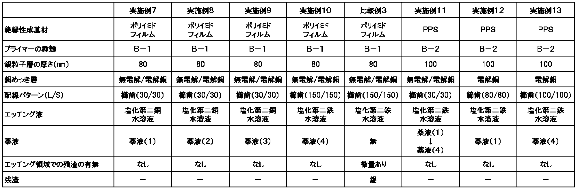
[エッチング領域(非回路)表面のエッチング残渣有無の確認]
上記で得られたプリント配線板のエッチング領域(非回路部)表面のエッチング残渣有無は、目視での白化部分有無確認の後、走査型電子顕微鏡(日本電子株式会社製「JSM-IT500」)、及び、付属のエネルギー分散形X線分析装置(EDS)で、観察と残渣種の分析を行った。
上記で得られたプリント配線板のエッチング領域(非回路部)表面のエッチング残渣有無は、目視での白化部分有無確認の後、走査型電子顕微鏡(日本電子株式会社製「JSM-IT500」)、及び、付属のエネルギー分散形X線分析装置(EDS)で、観察と残渣種の分析を行った。
a:回路部(差動配線パターン)
b:非回路部
c:洗浄領域
d:非洗浄領域
b:非回路部
c:洗浄領域
d:非洗浄領域
Claims (6)
- 絶縁性基材(A)上に、銀粒子を含有する銀粒子層(M1)を形成する工程1、
前記銀粒子層(M1)上に、めっき法によって、銅めっき層(M2)を形成する工程2、
前記銅めっき層(M2)上に回路パターンのレジストを形成し、非回路部の銅めっき層(M2)をエッチング除去して銅回路パターンを有する積層体を作製する工程3、
前記銅回路パターンを有する積層体を薬液で洗浄する工程4を有することを特徴とするプリント配線板の製造方法。 - 絶縁性基材(A)上に、プライマー層(B)を形成した後、銀粒子を含有する銀粒子層(M1)を形成する工程1’、
前記銀粒子層(M1)上に、めっき法によって、銅めっき層(M2)を形成する工程2、
前記銅めっき層(M2)上に回路パターンのレジストを形成し、非回路部の銅めっき層(M2)をエッチング除去して銅回路パターンを有する積層体を作製する工程3、
前記銅回路パターンを有する積層体を薬液で洗浄する工程4を有することを特徴とするプリント配線板の製造方法。 - 前記工程3におけるエッチング除去を、塩化第二鉄又は塩化第二銅を含有するエッチング液を用いて行う請求項1又は2記載のプリント配線板の製造方法。
- 前記工程4において用いる薬液が、カルボン酸及び過酸化水素を含有する水溶液である請求項1~3のいずれか1項記載のプリント配線板の製造方法。
- 前記工程4において用いる薬液が、チオ硫酸塩又はトリス(3-ヒドロキシアルキル)ホスフィンを含有する水溶液である請求項1~3のいずれか1項記載のプリント配線板の製造方法。
- 前記工程4が、チオ硫酸塩又はトリス(3-ヒドロキシアルキル)ホスフィンを含有する水溶液で洗浄した後、さらに、カルボン酸及び過酸化水素を含有する水溶液で洗浄する工程である請求項1~3のいずれか1項記載のプリント配線板の製造方法。
Applications Claiming Priority (2)
| Application Number | Priority Date | Filing Date | Title |
|---|---|---|---|
| JP2018239598 | 2018-12-21 | ||
| JP2018-239598 | 2018-12-21 |
Publications (1)
| Publication Number | Publication Date |
|---|---|
| WO2020130071A1 true WO2020130071A1 (ja) | 2020-06-25 |
Family
ID=71100876
Family Applications (1)
| Application Number | Title | Priority Date | Filing Date |
|---|---|---|---|
| PCT/JP2019/049799 Ceased WO2020130071A1 (ja) | 2018-12-21 | 2019-12-19 | プリント配線板の製造方法 |
Country Status (2)
| Country | Link |
|---|---|
| TW (1) | TW202035793A (ja) |
| WO (1) | WO2020130071A1 (ja) |
Cited By (3)
| Publication number | Priority date | Publication date | Assignee | Title |
|---|---|---|---|---|
| CN116438331A (zh) * | 2020-11-05 | 2023-07-14 | Dic株式会社 | 金属皮膜形成方法 |
| CN117769145A (zh) * | 2024-02-22 | 2024-03-26 | 深圳市盛鸿运科技有限公司 | 一种线路板蚀刻方法及线路板 |
| CN119815702A (zh) * | 2024-12-26 | 2025-04-11 | 黑龙江汇芯半导体有限公司 | 一种智能功率模块铝基覆铜板加工方法 |
Families Citing this family (1)
| Publication number | Priority date | Publication date | Assignee | Title |
|---|---|---|---|---|
| TWI841294B (zh) * | 2023-03-15 | 2024-05-01 | 國立中興大學 | 軟性電路板與其製作方法 |
Citations (5)
| Publication number | Priority date | Publication date | Assignee | Title |
|---|---|---|---|---|
| JPH10251878A (ja) * | 1997-03-14 | 1998-09-22 | Asahi Denka Kogyo Kk | 塩化銀除去剤 |
| WO2014045972A1 (ja) * | 2012-09-20 | 2014-03-27 | Dic株式会社 | 導電性材料及びその製造方法 |
| JP2014196556A (ja) * | 2013-03-07 | 2014-10-16 | Dic株式会社 | 導電性材料の製造方法及び導電性材料 |
| WO2015029478A1 (ja) * | 2013-08-29 | 2015-03-05 | 日立金属株式会社 | セラミックス回路基板の製造方法 |
| JP2017218664A (ja) * | 2016-06-10 | 2017-12-14 | 株式会社C−Ink | めっき下地用の組成物及びそれによるめっき下地 |
-
2019
- 2019-12-17 TW TW108146119A patent/TW202035793A/zh unknown
- 2019-12-19 WO PCT/JP2019/049799 patent/WO2020130071A1/ja not_active Ceased
Patent Citations (5)
| Publication number | Priority date | Publication date | Assignee | Title |
|---|---|---|---|---|
| JPH10251878A (ja) * | 1997-03-14 | 1998-09-22 | Asahi Denka Kogyo Kk | 塩化銀除去剤 |
| WO2014045972A1 (ja) * | 2012-09-20 | 2014-03-27 | Dic株式会社 | 導電性材料及びその製造方法 |
| JP2014196556A (ja) * | 2013-03-07 | 2014-10-16 | Dic株式会社 | 導電性材料の製造方法及び導電性材料 |
| WO2015029478A1 (ja) * | 2013-08-29 | 2015-03-05 | 日立金属株式会社 | セラミックス回路基板の製造方法 |
| JP2017218664A (ja) * | 2016-06-10 | 2017-12-14 | 株式会社C−Ink | めっき下地用の組成物及びそれによるめっき下地 |
Cited By (4)
| Publication number | Priority date | Publication date | Assignee | Title |
|---|---|---|---|---|
| CN116438331A (zh) * | 2020-11-05 | 2023-07-14 | Dic株式会社 | 金属皮膜形成方法 |
| CN117769145A (zh) * | 2024-02-22 | 2024-03-26 | 深圳市盛鸿运科技有限公司 | 一种线路板蚀刻方法及线路板 |
| CN117769145B (zh) * | 2024-02-22 | 2024-04-19 | 深圳市盛鸿运科技有限公司 | 一种线路板蚀刻方法及线路板 |
| CN119815702A (zh) * | 2024-12-26 | 2025-04-11 | 黑龙江汇芯半导体有限公司 | 一种智能功率模块铝基覆铜板加工方法 |
Also Published As
| Publication number | Publication date |
|---|---|
| TW202035793A (zh) | 2020-10-01 |
Similar Documents
| Publication | Publication Date | Title |
|---|---|---|
| JP6750766B2 (ja) | プリント配線板の製造方法 | |
| JP6766983B2 (ja) | プリント配線板の製造方法 | |
| JP6886629B2 (ja) | 金属パターンを有する成形体の製造方法 | |
| JP6667119B1 (ja) | プリント配線板用積層体及びそれを用いたプリント配線板 | |
| WO2020130071A1 (ja) | プリント配線板の製造方法 | |
| JP7260065B2 (ja) | セミアディティブ工法用積層体及びそれを用いたプリント配線板 | |
| JP7201130B2 (ja) | セミアディティブ工法用積層体及びそれを用いたプリント配線板 | |
| JPWO2020003881A1 (ja) | 金属パターンを有する成形体の製造方法 | |
| WO2022097484A1 (ja) | セミアディティブ工法用積層体及びそれを用いたプリント配線板 | |
| JP7371778B2 (ja) | セミアディティブ工法用積層体及びそれを用いたプリント配線板 | |
| JP7288230B2 (ja) | セミアディティブ工法用積層体及びそれを用いたプリント配線板 | |
| JP7332049B2 (ja) | セミアディティブ工法用積層体及びそれを用いたプリント配線板 | |
| TWI914436B (zh) | 半加成工法用積層體及其製造方法、以及使用該半加成工法用積層體之印刷配線板及其製造方法 | |
| WO2022097488A1 (ja) | セミアディティブ工法用積層体及びそれを用いたプリント配線板 | |
| WO2022097481A1 (ja) | セミアディティブ工法用積層体及びそれを用いたプリント配線板 |
Legal Events
| Date | Code | Title | Description |
|---|---|---|---|
| 121 | Ep: the epo has been informed by wipo that ep was designated in this application |
Ref document number: 19897651 Country of ref document: EP Kind code of ref document: A1 |
|
| NENP | Non-entry into the national phase |
Ref country code: DE |
|
| 122 | Ep: pct application non-entry in european phase |
Ref document number: 19897651 Country of ref document: EP Kind code of ref document: A1 |
|
| NENP | Non-entry into the national phase |
Ref country code: JP |