WO2020129526A1 - 電子デバイスの製造方法及びガラス基板 - Google Patents
電子デバイスの製造方法及びガラス基板 Download PDFInfo
- Publication number
- WO2020129526A1 WO2020129526A1 PCT/JP2019/045458 JP2019045458W WO2020129526A1 WO 2020129526 A1 WO2020129526 A1 WO 2020129526A1 JP 2019045458 W JP2019045458 W JP 2019045458W WO 2020129526 A1 WO2020129526 A1 WO 2020129526A1
- Authority
- WO
- WIPO (PCT)
- Prior art keywords
- glass substrate
- glass
- protective film
- film
- electronic device
- Prior art date
- Legal status (The legal status is an assumption and is not a legal conclusion. Google has not performed a legal analysis and makes no representation as to the accuracy of the status listed.)
- Ceased
Links
Images






Classifications
-
- C—CHEMISTRY; METALLURGY
- C03—GLASS; MINERAL OR SLAG WOOL
- C03C—CHEMICAL COMPOSITION OF GLASSES, GLAZES OR VITREOUS ENAMELS; SURFACE TREATMENT OF GLASS; SURFACE TREATMENT OF FIBRES OR FILAMENTS MADE FROM GLASS, MINERALS OR SLAGS; JOINING GLASS TO GLASS OR OTHER MATERIALS
- C03C17/00—Surface treatment of glass, not in the form of fibres or filaments, by coating
- C03C17/22—Surface treatment of glass, not in the form of fibres or filaments, by coating with other inorganic material
- C03C17/23—Oxides
- C03C17/25—Oxides by deposition from the liquid phase
-
- C—CHEMISTRY; METALLURGY
- C03—GLASS; MINERAL OR SLAG WOOL
- C03C—CHEMICAL COMPOSITION OF GLASSES, GLAZES OR VITREOUS ENAMELS; SURFACE TREATMENT OF GLASS; SURFACE TREATMENT OF FIBRES OR FILAMENTS MADE FROM GLASS, MINERALS OR SLAGS; JOINING GLASS TO GLASS OR OTHER MATERIALS
- C03C17/00—Surface treatment of glass, not in the form of fibres or filaments, by coating
- C03C17/28—Surface treatment of glass, not in the form of fibres or filaments, by coating with organic material
-
- G—PHYSICS
- G02—OPTICS
- G02F—OPTICAL DEVICES OR ARRANGEMENTS FOR THE CONTROL OF LIGHT BY MODIFICATION OF THE OPTICAL PROPERTIES OF THE MEDIA OF THE ELEMENTS INVOLVED THEREIN; NON-LINEAR OPTICS; FREQUENCY-CHANGING OF LIGHT; OPTICAL LOGIC ELEMENTS; OPTICAL ANALOGUE/DIGITAL CONVERTERS
- G02F1/00—Devices or arrangements for the control of the intensity, colour, phase, polarisation or direction of light arriving from an independent light source, e.g. switching, gating or modulating; Non-linear optics
- G02F1/01—Devices or arrangements for the control of the intensity, colour, phase, polarisation or direction of light arriving from an independent light source, e.g. switching, gating or modulating; Non-linear optics for the control of the intensity, phase, polarisation or colour
- G02F1/13—Devices or arrangements for the control of the intensity, colour, phase, polarisation or direction of light arriving from an independent light source, e.g. switching, gating or modulating; Non-linear optics for the control of the intensity, phase, polarisation or colour based on liquid crystals, e.g. single liquid crystal display cells
-
- G—PHYSICS
- G02—OPTICS
- G02F—OPTICAL DEVICES OR ARRANGEMENTS FOR THE CONTROL OF LIGHT BY MODIFICATION OF THE OPTICAL PROPERTIES OF THE MEDIA OF THE ELEMENTS INVOLVED THEREIN; NON-LINEAR OPTICS; FREQUENCY-CHANGING OF LIGHT; OPTICAL LOGIC ELEMENTS; OPTICAL ANALOGUE/DIGITAL CONVERTERS
- G02F1/00—Devices or arrangements for the control of the intensity, colour, phase, polarisation or direction of light arriving from an independent light source, e.g. switching, gating or modulating; Non-linear optics
- G02F1/01—Devices or arrangements for the control of the intensity, colour, phase, polarisation or direction of light arriving from an independent light source, e.g. switching, gating or modulating; Non-linear optics for the control of the intensity, phase, polarisation or colour
- G02F1/13—Devices or arrangements for the control of the intensity, colour, phase, polarisation or direction of light arriving from an independent light source, e.g. switching, gating or modulating; Non-linear optics for the control of the intensity, phase, polarisation or colour based on liquid crystals, e.g. single liquid crystal display cells
- G02F1/133—Constructional arrangements; Operation of liquid crystal cells; Circuit arrangements
- G02F1/1333—Constructional arrangements; Manufacturing methods
-
- G—PHYSICS
- G09—EDUCATION; CRYPTOGRAPHY; DISPLAY; ADVERTISING; SEALS
- G09F—DISPLAYING; ADVERTISING; SIGNS; LABELS OR NAME-PLATES; SEALS
- G09F9/00—Indicating arrangements for variable information in which the information is built-up on a support by selection or combination of individual elements
-
- G—PHYSICS
- G09—EDUCATION; CRYPTOGRAPHY; DISPLAY; ADVERTISING; SEALS
- G09F—DISPLAYING; ADVERTISING; SIGNS; LABELS OR NAME-PLATES; SEALS
- G09F9/00—Indicating arrangements for variable information in which the information is built-up on a support by selection or combination of individual elements
- G09F9/30—Indicating arrangements for variable information in which the information is built-up on a support by selection or combination of individual elements in which the desired character or characters are formed by combining individual elements
Definitions
- the present invention relates to a method for manufacturing an electronic device and a glass substrate, and more particularly to a technique for preventing a decrease in strength of the glass substrate during manufacturing.
- the strength of the glass substrate is significantly reduced, and the electronic device is damaged by the bending load caused by the impact or the pressure caused by the drop and the glass substrate as a starting point. There is a problem that the fear increases.
- Patent Document 1 discloses a method of manufacturing a liquid crystal display panel provided with a reinforcing structure. This manufacturing method is performed in the following procedure. First, in a state where a predetermined laminated structure is formed on one surface of each of the two glass substrates facing each other, the two glass substrates are bonded together, and a liquid crystal is applied between the bonded two glass substrates. The encapsulation forms a liquid crystal display panel. After that, by forming a hard coat layer made of a silicon-based material on the other surface of each glass substrate that faces the outside of the liquid crystal display panel, a liquid crystal display panel having a reinforcing structure on the outside is manufactured. ..
- a glass substrate of this type has a lower surface of a lower surface by a predetermined carrying device toward a process for manufacturing a liquid crystal panel after finishing the processing of the glass substrate itself. At least a part of the sheet is transported while being supported. Further, in a process of manufacturing a liquid crystal display panel using the glass substrate such as a process of bonding the glass substrate, the glass substrates are bonded with the lower surface being supported.
- the technical issue to be solved is to prevent or suppress the situation where the surface of the glass substrate is scratched during the manufacturing of the electronic device and secure the strength of the electronic device.
- this manufacturing method is a method for manufacturing an electronic device including a preparatory step of preparing a glass substrate and a manufacturing step of manufacturing an electronic device using the glass substrate. Is characterized in that a glass substrate on which a protective film for protecting the surface of is protected is prepared, and an electronic device is manufactured by supporting a side of the glass substrate on which the protective film is formed in a manufacturing process.
- a glass substrate with a protective film in which a protective film for protecting one surface is formed on one surface of the glass substrate in advance is prepared, and An electronic device was manufactured by supporting the side of the glass substrate on which the protective film was formed.
- the protective film may be a low friction film having a static friction coefficient lower than that of the glass substrate.
- the protective film By thus forming the protective film as a low-friction film exhibiting a coefficient of static friction lower than that of the glass substrate, the glass substrate can be made more slippery during transportation or panel production. Therefore, it is possible to more effectively prevent the glass substrate from being scratched.
- the low-friction film may have a coefficient of static friction of 0.42 or less in the method for manufacturing an electronic device according to the present invention.
- the above-mentioned static friction coefficient is a value obtained by measuring the static friction coefficient between the protective film formed on the glass substrate and the wrapping film LWFS-30#4000 manufactured by Sankyo Rikagaku Co., Ltd. according to JIS K 7125:1999. Shall be pointed out.
- this glass substrate is a glass substrate for electronic devices, and is characterized in that a protective film for protecting the non-guaranteed surface is formed on the non-guaranteed surface.
- a protective film for protecting the non-guaranteed surface is formed on the non-guaranteed surface.
- each process such as transportation and processing of the glass substrate is performed with the surface (guarantee surface) for which the required quality is to be guaranteed as far as possible.
- the non-guaranteed surface located on the back side of the guarantee surface becomes the contacted surface during each process such as transportation or processing.
- the protective film can prevent or suppress scratches on the glass substrate surface. Therefore, it becomes possible to secure the strength of the electronic device having this glass substrate.
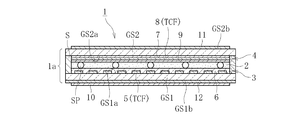
- FIG. 1 is a cross-sectional view of a liquid crystal display panel according to an exemplary embodiment of the present invention.
- 3 is a flowchart showing a procedure of a method for manufacturing the liquid crystal display panel shown in FIG. 1.
- 3 is a flowchart showing the procedure of the preparation process shown in FIG. 2.
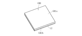
- It is a perspective view of the 1st mother glass prepared for the preparation process shown in FIG.
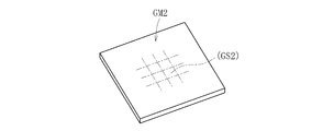
- FIG. 3 is a perspective view of a second mother glass prepared in the preparation process shown in FIG. 2.
- 3 is a flowchart showing the procedure of the manufacturing process shown in FIG. 2.
- It is a perspective view of the 1st laminated body containing the 1st mother glass prepared for the assembly process shown in FIG.
- FIG. 1 shows a liquid crystal display panel 1 as an example of an electronic device to which the present invention is applied.
- This liquid crystal display panel 1 includes a first glass substrate GS1, a second glass substrate GS2, a spacer SP, a liquid crystal layer 2 arranged between the first glass substrate GS1 and the second glass substrate GS2, A first laminated portion 3 arranged between the one glass substrate GS1 and the liquid crystal layer 2 and a second laminated portion 4 arranged between the second glass substrate GS2 and the liquid crystal layer 2.
- the shapes of the first glass substrate GS1 and the second glass substrate GS2 are rectangular in the present embodiment, but of course, are not limited to this shape.
- silicate glass and silica glass are used, preferably borosilicate glass, soda lime glass, aluminosilicate glass, and chemically strengthened glass are used, and most preferably alkali-free glass. Is used.
- non-alkali glass is a glass that does not substantially contain an alkali component (alkali metal oxide), and specifically, a glass in which the weight ratio of the alkali components is 3000 ppm or less. is there.
- the weight ratio of the alkaline component in the present invention is preferably 1000 ppm or less, more preferably 500 ppm or less, and most preferably 300 ppm or less.
- Each of the glass substrates GS1 and GS2 can be formed by a known float method, roll-out method, slot down draw method, redraw method, or the like, but it is preferably formed by the overflow down draw method.
- each glass substrate GS1, GS2 is set to 1000 ⁇ m or less, preferably 10 ⁇ m or more and 700 ⁇ m or less, more preferably 20 ⁇ m or more and 500 ⁇ m or less, and most preferably 200 ⁇ m or more and 500 ⁇ m or less.
- the first laminated portion 3 is formed on the inner surface GS1a of the first glass substrate GS1 (the inner side here means the inner side of the liquid crystal display panel 1), and is made of, for example, a transparent conductive film TCF.
- the first alignment layer 6 is formed on the first electrode layer 5 and the first electrode layer 5 (pixel electrode).
- the material of the first electrode layer 5 is not particularly limited as long as it has translucency and conductivity.
- the first electrode layer 5 is formed of, for example, indium-doped tin oxide (ITO), fluorine-doped tin oxide (FTO), indium zinc oxide (IZO), aluminum-doped zinc oxide (AZO), or the like.
- the first alignment film 6 is a transparent film formed of, for example, a polyimide film or other material in which minute grooves are formed by rubbing.
- the liquid crystal molecules contained in the liquid crystal layer 2 can be aligned at a pretilt angle by the action of the first alignment film 6.
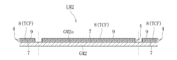
- the second laminated portion 4 is formed on the inner surface GS2a of the second glass substrate GS2, and includes, for example, a color filter layer 7, a second electrode layer 8 (counter electrode) formed of a transparent conductive film TCF, and It is composed of two alignment films 9.
- the color filter layer 7 is formed of a black matrix and a plurality of colored pixels.
- the material, thickness and sheet resistance of the second electrode layer 8 are the same as those of the first electrode layer 5.
- the configuration, material and thickness of the second alignment film 9 are the same as those of the first alignment film 6.
- the seal portion S is a frame-shaped seal member that surrounds the liquid crystal layer 2.
- the seal portion S is formed of a seal material such as a UV curable resin or a thermosetting resin, but is not limited to any of these materials.
- the spacer SP has, for example, a spherical shape and is made of resin or silica.
- the liquid crystal layer 2 is made of nematic liquid crystal or the like.
- the liquid crystal layer 2 is formed in a space defined by the first glass substrate GS1, the second glass substrate GS2, and the seal portion S.
- the first polarizing plate 10 is arranged on the outermost side of the first glass substrate GS1, and the second polarizing plate 11 is arranged on the outermost side of the second glass substrate GS2.
- a retardation plate may be provided in addition to these polarizing plates 10 and 11.
- the protective film 12 that protects the outer surface GS1b is formed on the surface of the first glass substrate GS1 opposite to the side on which the first electrode layer 5 is formed (that is, the outer surface GS1b). Has been done. In this case, the protective film 12 is arranged between the first glass substrate GS1 and the first polarizing plate 10.
- the protective film 12 is configured to have a lower friction coefficient (static friction coefficient, dynamic friction coefficient) than the first glass substrate GS1 (low friction film). Specifically, it is formed of a material having a coefficient of friction lower than that of glass.
- the static friction coefficient of the protective film 12 should be 0.42 or less, and 0.35 or less. It is preferable to show, and it is more preferable to show 0.30 or less.
- a fluorine-based material can be exemplified.
- the protective film 12 when the protective film 12 having the above configuration is selected in terms of characteristics and performance, for example, the protective film 12 may be a functional film.
- the functional film referred to here is, for example, an antireflection function (AR), a fingerprint antifouling function (AF), a glare prevention (antiglare) with respect to the glass substrate GS1 on which the protective film 12 is formed.
- Function (AG), infrared ray cutting function (IR), conductivity imparting function, cold mirror function, ultraviolet ray cutting function (UV), and the like are included in the thin film.
- a thin film (antifouling film) having a stain prevention function capable of forming a film by spraying is preferable.
- the protective film 12 when the protective film 12 having the above structure is selected in terms of material, the protective film 12 may be a thin film (organic film) formed of an organic material, or SiO 2 , Nb 2 O 5 , SiNx, It may be a thin film (inorganic film) formed of an inorganic material such as ITO.
- the manufacturing method of the liquid crystal display panel 1 includes a preparation step S1 of preparing a predetermined glass substrate and a manufacturing step of manufacturing the liquid crystal display panel 1 using the predetermined glass substrate. And S2.
- the preparation step S1 includes an acquisition step S3 for acquiring the first and second mother glasses GM1 and GM2 and at least one of the acquired mother glasses GM1 and GM2 (this embodiment. Then, there is a protective film forming step S4 of forming the protective film 12 on the first mother glass GM1).
- both the first and second mother glasses GM1 and GM2 are glass substrates to be the first and second glass substrates GS1 and GS2 shown in FIG.
- the first and second glass substrates GS1 and GS2 shown in FIG. 1 are cut out from the first and second mother glasses GM1 and GM2 by so-called multiple cutting after being bonded (after the assembling step S6 described later). Glass substrate (see the area surrounded by the alternate long and short dash line in FIGS. 4A and 4B).
- each mother glass GM1, GM2 are basically the same as the thickness dimension, material, and molding means of the glass substrates GS1, GS2 described above.
- the first and second laminated portions 3 and 4 are respectively formed on one surface GM1a and GM2a of each mother glass GM1 and GM2, and the protective film 12 is formed on the other surface GM1b of the first mother glass GM1.
- the dashed-dotted line in FIGS. 4A and 4B is a planned cutting line in the cutting step S7 described later.
- the alternate long and short dash line in FIGS. 7A to 9B is also the same planned cutting line.
- one surface GM1a of the first mother glass GM1 on which the first laminated portion 3 (see FIG. 1) is formed is formed on the surface (the other surface GM1b) opposite to the surface GM1a.
- the protective film 12 is formed.
- the means for forming the protective film 12 is arbitrary, and a known film forming means can be appropriately selected according to the type of the protective film 12.
- the protective film 12 is formed of an antifouling film such as an AF coat
- the protective film 12 is formed on the entire surface of the other surface GM1b by means such as spraying. Thereby, as shown in FIG.
- the first mother glass GM1 (glass substrate with a protective film) in which the protective film 12 is formed on the other surface GM1b is obtained.
- the other surface GM1b of the first mother glass GM1 is the outer surface GS1b of the first glass substrate GS1 to be cut out (the outer side here means the outer side of the liquid crystal display panel 1).
- the outer surface GS1b is also a non-guaranteed surface.
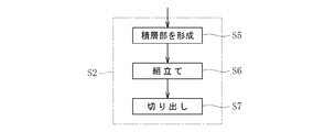
- the manufacturing step S2 of the liquid crystal display panel 1 includes a laminated portion forming step S5, an assembling step S6, and a cutting step S7, which are manufacturing-related processing steps (see FIG. 6).
- the first laminated portion 3 is formed on the one surface GM1a side of the first mother glass GM1 on which the protective film 12 is formed, and the one surface GM2a of the second mother glass GM2 is formed.
- the second laminated portion 4 is formed on the substrate (see FIGS. 7A and 7B).
- the first laminated portion 3 the first electrode layer 5 formed of the transparent conductive film TCF and the first alignment film 6 are formed on the one surface GM1a of the first mother glass GM1.
- a color filter layer 7, a second electrode layer 8 formed of a transparent conductive film TCF, and a second alignment film 9 are formed on one surface GM2a of the second mother glass GM2. To be done.
- the transparent conductive film TCF is formed on the one surface GM1a of the first mother glass GM1 on which the protective film 12 is formed. ..
- a photoresist photosensitive resin
- the resist layer is covered with a photomask and irradiated with light such as ultraviolet rays to form a photomask.
- the formed pattern having the predetermined shape is transferred to the resist layer.
- the first mother glass GM1 formed on the GM1a is obtained (see FIGS. 7A and 8A).
- the first mother glass GM1 in this state is also referred to as the first stacked body LM1.
- the procedure for forming the second laminated portion 4 on the second mother glass GM2 will be described. First, for example, a black matrix is formed on one surface GM2a of the second mother glass GM2, and then a color resist coating step, an exposure step, and a development step are performed.
- the color filter layer 7 corresponding to a plurality of colors (RGB) is formed by repeating the baking process. Then, after forming the transparent conductive film TCF on the surface of the color filter layer 7, the second electrode having a predetermined electrode pattern by the transparent conductive film TCF is formed by performing the same patterning process as that of the first mother glass GM1 if necessary.
- the layer 8 is formed (the extending direction of each electrode is orthogonal to the first electrode layer 5 and the second electrode layer 8).
- the second laminated portion 4 formed by covering the second electrode layer 8 with the second alignment film 9 has one surface.
- the second mother glass GM2 in a state of being formed on the GM2a is obtained (see FIGS. 7B and 8B).
- the second mother glass GM2 in this state is also referred to as the second stacked body LM2.
- the first electrode layer 5 has a source electrode, a gate electrode, a drain electrode, an insulating layer, a switching element (TFT, etc.). It is formed by photolithography or another method.
- the transparent conductive film TCF can be formed by any means, and can be formed by a known film forming method such as a sputtering method, a vapor deposition method, a CVD method or the like. Further, the type of the transparent conductive film TCF that can be formed is arbitrary, and an example thereof is an ITO film.
- the means for forming the first and second alignment films 6 and 9 is also arbitrary, and can be formed by a known means such as spin coating. Further, rubbing treatment may be applied to each of the alignment films 6 and 9. By this rubbing treatment, although not shown, innumerable minute groove portions are formed on the surfaces of the alignment films 6 and 9.
- (S6) Assembly Step the assembly 13 of the liquid crystal display panel 1 is assembled.
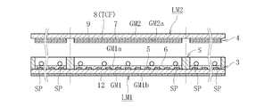
- the first laminated body LM1 and the second laminated body LM2 are opposed to each other, and a sealing material forming a seal portion S and a spacer SP are supplied between the laminated bodies LM1 and LM2.
- the seal material forming the seal portion S is applied in advance on the first alignment film 6 of the first stacked body LM1 so that the seal portion S has a lattice shape in a plan view (see FIG. 9A).
- a plurality of regions surrounded by the seal portion S that is, a plurality of regions serving as spaces (see FIG.
- the first stacked body LM1 is arranged below the second stacked body LM2, and the first stacked body LM1 and the second stacked body LM2 are arranged so that the first alignment film 6 and the second alignment film 9 face each other.
- the protective film 12 is placed on the lowermost side of the first stacked body LM1.
- the sealing material S may not be applied on the cut line.
- the sealing material S may have a divided structure in the width direction (left and right direction of the paper surface of FIG. 9A), and a space may be provided between the divided sealing materials S.
- the spacer SP is sandwiched between both stacked bodies LM1 and LM2, and is applied in advance on the first stacked body LM1.
- the seal material of the seal portion S that has been set is brought into contact with the second stacked body LM2 (see FIG. 9B).
- the sealing portion S is formed between the stacked bodies LM1 and LM2, and The laminated bodies LM1 and LM2 that come into contact with the sealing material are adhesively fixed to the sealing portion S.
- the first stacked body LM1 and the second stacked body LM2 are bonded to each other via the seal portion S.
- the sealing material so that the seal portion S has a lattice shape in a plan view, in the state where the first stacked body LM1 and the second stacked body LM2 are attached to each other, A plurality of liquid crystal layers 2 are formed in a region surrounded by the one stacked body LM1, the second stacked body LM2, and the seal portion S (see FIG. 9B).
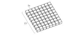
- the assembly 13 of the liquid crystal display panel 1 including the plurality of liquid crystal layers 2 formed between the first stacked body LM1 and the second stacked body LM2 is assembled (see FIG. 10).
- the first stacked body LM1 is fed from below by, for example, a roller of a transporting device for loading and unloading the first stacked body LM1 and an elevating member for raising the first stacked body LM1. Supported.
- (S7) Cutting Step After that, the assembly 13 is cut along a predetermined planned cutting line (for example, a planned cutting line indicated by a chain line in FIGS. 7 to 9) to attach the pair of glass substrates GS1 and GS2 to each other.
- the substrates 1a of the plurality of liquid crystal display panels 1 that are combined are cut out (see FIG. 11).
- the polarizing plates 10 and 11 are fixed on both surfaces of the base body 1a, and necessary electronic parts and the like are mounted, so that the liquid crystal display panel 1 shown in FIG. 1 is manufactured.
- the glass substrate with the protective film (the first mother glass GM1 on which the protective film 12 is formed) is prepared before the production step S2.
- the liquid crystal display panel 1 is manufactured with the side of the glass substrate on which the protective film 12 is formed being supported.
- the assembly 13 of the liquid crystal display panel 1 is scheduled to be cut.
- the protective film 12 prevents or suppresses the surface of the first mother glass GM1 from being scratched. can do. Therefore, it becomes possible to secure the strength of the liquid crystal display panel 1 having the first glass substrate GS1 obtained by cutting out the first mother glass GM1.
- first laminated body LM1 first mother glass GM1
- first mother glass GM1 first mother glass GM1
- the friction between the rollers and the first mother glass GM1 side is formed.
- the protective film 12 on the support side (the other surface GM1b side) of the first mother glass GM1
- the first mother glass GM1 is rubbed by rubbing when positioning is stopped. It is possible to prevent or suppress scratching.
- the method for manufacturing an electronic device and the glass substrate according to the present invention are not limited to the above-described embodiments.
- the manufacturing method and the glass substrate can take various forms within the scope of the present invention.
- the protective film 12 is formed on the entire surface of the other surface GM1b of the first mother glass GM1 is illustrated, but the present invention is not limited to this.
- the rollers and the lifting members in the assembling step S6 the supporting form of the members that support the first mother glass GM1 in the laminated portion forming step S5, and the members that support the first mother glass GM1 during transportation between these steps. It is also possible to form the protective film 12 on a predetermined part of the other surface GM1b depending on the support form and the like.
- the elevating member as the supporting member is raised to bring the first stacked body LM1 closer to the second stacked body LM2 is illustrated, but the first stacked body LM1 in a state of being supported from below, for example.
- the second stacked body LM2 may be lowered from above to sandwich the spacer SP.
- the movement form is arbitrary as long as the spacer SP can be sandwiched by the relative movement of the first stacked body LM1 and the second stacked body LM2.
- the protective film 12 is formed only on the first mother glass GM1 in the preparation step S1 is illustrated, but of course, the protective film 12 may be formed on both mother glasses GM1 and GM2.
- the protective film 12 is formed on one mother glass GM1, and the first and second laminated portions 3 and 4 are formed on both mother glasses GM1 and GM2 to form the first and second laminated bodies.
- the procedure for obtaining the liquid crystal display panel 1 after forming the assembly 13 of the liquid crystal display panel 1 by forming the LM1 and LM2 and adhering the produced laminated bodies LM1 and LM2 to each other is illustrated, but of course, It is also possible to take steps other than.
- the protective film 12 may be formed before or after cutting.
- the case where the protective film 12 is formed on the mother glass in the preparation step S1 and the protective film 12 is not formed again in the preparation step S2 has been described as an example, but the protection film 12 may be formed in the preparation step S2 if necessary. A step of forming again may be provided.
- a rectangular single-wafer glass substrate is illustrated as each of the mother glasses GM1 and GM2, but it is of course possible to form the protective film 12 on the mother glasses GM1 and GM2 having other forms.
- a glass substrate (glass film) that is thin enough to be wound may be used as the mother glass, and the protective film 12 may be formed on this glass film.
- the step of forming the protective film 12 on the glass film can be performed by continuously performing a film forming process on one surface of the glass film supplied by a so-called roll-to-roll method. After the protective film 12 is continuously formed, the protective film 12 may be cut and the laminated portion forming step S5 and the assembling step S6 may be sequentially performed.
- the present invention can be applied to the case of manufacturing other electronic devices.
- the present invention can be applied to the case of manufacturing an organic EL lighting (element) or a touch panel as an electronic device.
- OA-11 manufactured by Nippon Electric Glass Co., Ltd. was prepared as a glass substrate, and as a material for the protective film, an AF coating agent manufactured by Daikin Industries, Ltd. OPTOOL UF503 and 3M Japan Co., Ltd. A mixture with Novec 72DE was used. After the glass substrate is washed, the mixed solution is spray-coated on the glass substrate, wiped off, dried at room temperature, and then heat-treated at 150° C. for 30 minutes to perform AF as a protective film on the surface of the glass substrate. A glass substrate with a coat formed was obtained.
- the static friction coefficient between this glass substrate and the wrapping film LWFS-30#4000 manufactured by Sankyo Rikagaku Co., Ltd. was measured according to JIS K 7125:1999, and it was 0.26.
- a scratch test was performed on a glass substrate with a protective film (Example) and a glass substrate without a protective film (Comparative Example) for the purpose of reproducing scratches produced during manufacturing.
- the scratch test was performed by rubbing a wrapping film LWFS-30#4000 manufactured by Sankyo Rikagaku Co., Ltd. on the surface of each glass substrate.
- a scratch test was conducted by rubbing the lapping film on the side on which the protective film was formed. The conditions at this time were a surface load of 500 g, a moving speed of 3 m/min, and a rubbing frequency of 10 reciprocations.
- the glass substrate with a protective film after scratching was set as Example 1.
- a glass substrate without a protective film after scratching was used as Comparative Example 1.
- the breaking load in the ring-on-ring test was measured for the above-mentioned three types of glass substrates (examples and comparative examples).
- the conditions at this time were that the diameter of the piston side ring was 12.5 mm, the diameter of the support side ring was 25 mm, and the descending speed of the piston side ring was 0.5 mm/s.
- the above-mentioned scratch test and ring-on-ring test were carried out 30 times for each glass substrate, and the median value of the measured breaking load [N] was taken as the evaluation value.
Landscapes
- Physics & Mathematics (AREA)
- Chemical & Material Sciences (AREA)
- General Physics & Mathematics (AREA)
- Engineering & Computer Science (AREA)
- Nonlinear Science (AREA)
- Geochemistry & Mineralogy (AREA)
- Crystallography & Structural Chemistry (AREA)
- Optics & Photonics (AREA)
- Life Sciences & Earth Sciences (AREA)
- Chemical Kinetics & Catalysis (AREA)
- General Chemical & Material Sciences (AREA)
- Theoretical Computer Science (AREA)
- Materials Engineering (AREA)
- Organic Chemistry (AREA)
- Liquid Crystal (AREA)
- Mathematical Physics (AREA)
- Devices For Indicating Variable Information By Combining Individual Elements (AREA)
- Surface Treatment Of Glass (AREA)
Abstract
ガラス基板GS1,GS2を有する電子デバイス1の製造方法は、ガラス基板GS1の一方の表面GS1bに、一方の表面GS1bを保護する保護膜12が形成されたガラス基板GS1を準備する準備工程S1と、ガラス基板GS1を用いて電子デバイス1を作製する作製工程S2とを備える。作製工程S2では、ガラス基板GS1の保護膜12が形成された側を支持して電子デバイス1を作製する。
Description
本発明は、電子デバイスの製造方法及びガラス基板に関し、特に製造時におけるガラス基板の強度低下を防止するための技術に関する。
近年、省スペース化の観点から、液晶ディスプレイ、有機ELディスプレイ等のフラットパネルディスプレイや薄膜電池、タッチパネル、有機EL照明といった各種電子デバイスが普及している。これらの電子デバイスでは、さらなる薄型化が要請される。この薄型化を推進するためには、電子デバイスに使用されるガラス基板を一層薄型化する必要がある。
ところが、上述のように電子デバイスを構成するガラス基板を薄くした場合、ガラス基板の強度が大幅に低下するため、落下による衝撃や押圧による曲げ荷重でガラス基板が起点となって電子デバイスが破損するおそれが高まるといった問題がある。
そこで、例えば特許文献1には、補強構造を設けた液晶ディスプレイパネルの製造方法が開示されている。この製造方法は、以下の手順で行われる。まず、二枚のガラス基板の互いに対向する一方の表面にそれぞれ所定の積層構造を形成した状態で、当該二枚のガラス基板を貼り合わせると共に、貼り合わせた二枚のガラス基板の間に液晶を封入することで、液晶ディスプレイパネルを形成する。然る後、液晶ディスプレイパネルの外側を指向する各ガラス基板の他方の表面に、シリコン系材料で形成されるハードコート層を形成することで、外側に補強構造を設けた液晶ディスプレイパネルを製造する。
ここで、実際に電子デバイスの製造工程におけるガラス基板の強度低下の原因を調査したところ、ガラス基板の薄肉化だけでなく、その製造過程におけるガラス基板の取扱いに問題があることが判明した。液晶ディスプレイパネルの製造工程を例にとると、この種のガラス基板は、ガラス基板自体の加工を終えた後、液晶パネルを作製するための工程に向けて所定の搬送装置により下側の表面の少なくとも一部を支持された状態で搬送される。また、ガラス基板の貼り合わせ工程など当該ガラス基板を用いて液晶ディスプレイパネルを作製する工程においては、下側の表面を支持された状態でガラス基板の貼り合わせが行われる。そのため、搬送時又はパネル作製時に、ガラス基板の被支持面(下側の表面)とガラス基板を支持する部材等との間に擦れが生じ、この擦れに起因して被支持面に傷が付くことが判明した。これでは、たとえ特許文献1に記載の製造方法を適用したとしても、補強構造を設ける前にガラス基板の表面に傷が付くことが避けられないため、新たな対策が必要となる。
以上の事情に鑑み、電子デバイスの製造時にガラス基板の表面に傷が付く事態を防止又は抑制して、電子デバイスの強度を確保することを、解決すべき技術課題とする。
前記課題の解決は、本発明に係る電子デバイスの製造方法により達成される。すなわち、この製造方法は、ガラス基板を準備する準備工程と、ガラス基板を用いて電子デバイスを作製する作製工程とを備えた電子デバイスの製造方法であって、準備工程で、ガラス基板として、一方の表面を保護する保護膜が形成されたガラス基板を準備し、作製工程で、ガラス基板の保護膜が形成された側を支持して電子デバイスを作製する点をもって特徴付けられる。
このように、本発明に係る電子デバイスの製造方法では、予めガラス基板の一方の表面に、一方の表面を保護する保護膜が形成された保護膜付きガラス基板を準備すると共に、この保護膜付きガラス基板の保護膜が形成された側を支持して電子デバイスを作製するようにした。このようにすれば、ガラス基板の搬送時、又はガラス基板を用いた電子デバイスの作製工程時にガラス基板と支持部材との間に擦れが生じた場合であっても、保護膜によりガラス基板表面に傷が付くのを防止又は抑制することができる。よって、このガラス基板を有する電子デバイスの強度(例えば曲げ強度)を確保することが可能となる。
また、本発明に係る電子デバイスの製造方法において、保護膜は、ガラス基板よりも低い静摩擦係数を示す低摩擦膜であってもよい。
このように、保護膜を、ガラス基板よりも低い静摩擦係数を示す低摩擦膜とすることによって、搬送時又はパネル作製時にガラス基板をより滑り易くすることができる。よって、ガラス基板に傷が付くのをより効果的に抑制することが可能となる。
また、保護膜が低摩擦膜である場合、本発明に係る電子デバイスの製造方法において、低摩擦膜の静摩擦係数が、0.42以下であってもよい。
具体的に、静摩擦係数が0.42以下の保護膜(低摩擦膜)を用いることによって、ガラス基板表面と相手面との十分な滑りを確保することができるので、ガラス基板の表面に傷が付くのを十分に抑制して電子デバイスに必要な強度を確保することが可能となる。なお、前述の静摩擦係数は、ガラス基板に成膜した保護膜と、三共理化学株式会社製ラッピングフィルムLWFS-30#4000との間の静摩擦係数を、JIS K 7125:1999に準拠して測定した値を指すものとする。
また、前記課題の解決は、本発明に係るガラス基板によっても達成される。すなわち、このガラス基板は、電子デバイス用のガラス基板であって、非保証面に、非保証面を保護する保護膜が形成されている点をもって特徴付けられる。
このように、本発明に係るガラス基板では、その非保証面に、非保証面を保護する保護膜を形成した。通常、この種のガラス基板においては、所要の品質を保証すべき面(保証面)をなるべく非接触状態としてガラス基板の搬送、加工等の各工程が行われる。この場合、保証面の裏側に位置する非保証面が搬送時又は加工等の各工程時における被接触面となる。よって、この非保証面を保護膜で保護したガラス基板であれば、ガラス基板の搬送時、又は電子デバイスの作製工程時にガラス基板の非保証面とこの非保証面に接触する部材との間に擦れが生じた場合であっても、保護膜によりガラス基板表面に傷が付くのを防止又は抑制することができる。よって、このガラス基板を有する電子デバイスの強度を確保することが可能となる。
以上に述べたように、本発明に係る電子デバイスの製造方法及びガラス基板によれば、電子デバイスの製造時にガラス基板の表面に傷が付く事態を防止又は抑制して、電子デバイスの強度を確保することが可能となる。
以下、本発明の一実施形態を説明する。
図1は、本発明の適用対象となる電子デバイスの一例としての液晶ディスプレイパネル1を示している。この液晶ディスプレイパネル1は、第一ガラス基板GS1と、第二ガラス基板GS2と、スペーサSPと、第一ガラス基板GS1と第二ガラス基板GS2との間に配設される液晶層2と、第一ガラス基板GS1と液晶層2との間に配設される第一積層部3と、第二ガラス基板GS2と液晶層2との間に配設される第二積層部4とを備える。
第一ガラス基板GS1及び第二ガラス基板GS2の形状は、本実施形態では矩形状であるが、もちろんこの形状には限定されない。各ガラス基板GS1,GS2の材質としては、ケイ酸塩ガラス、シリカガラスが用いられ、好ましくはホウ珪酸ガラス、ソーダライムガラス、アルミノ珪酸塩ガラス、化学強化ガラスが用いられ、最も好ましくは無アルカリガラスが用いられる。各ガラス基板GS1,GS2として無アルカリガラスを使用することで、化学的に安定なガラスとすることができる。ここで、無アルカリガラスとは、アルカリ成分(アルカリ金属酸化物)が実質的に含まれていないガラスのことであって、具体的には、アルカリ成分の重量比が3000ppm以下のガラスのことである。本発明におけるアルカリ成分の重量比は、好ましくは1000ppm以下であり、より好ましくは500ppm以下であり、最も好ましくは300ppm以下である。
各ガラス基板GS1,GS2は、公知のフロート法、ロールアウト法、スロットダウンドロー法、リドロー法等により成形できるが、オーバーフローダウンドロー法によって成形されていることが好ましい。
各ガラス基板GS1,GS2の厚みは、1000μm以下とされ、好ましくは10μm以上でかつ700μm以下であり、より好ましくは20μm以上でかつ500μm以下であり、最も好ましくは200μm以上でかつ500μm以下である。
第一積層部3は、第一ガラス基板GS1の内側表面GS1a(ここでいう内側とは、液晶ディスプレイパネル1の内側を意味する。)に形成されるもので、例えば透明導電膜TCFにより構成される第一電極層5(画素電極)と、第一電極層5上に積層される第一配向膜6とで構成される。
第一電極層5(透明導電膜TCF)の材質としては、透光性及び導電性を有するものであれば、特に限定されない。第一電極層5は、例えば、インジウムドープスズ酸化物(ITO)、フッ素ドープスズ酸化物(FTO)、インジウム亜鉛酸化物(IZO)、アルミニウムドープ亜鉛酸化物(AZO)等で形成される。
第一配向膜6は、例えばラビング処理で微小な溝部が形成されたポリイミド膜その他の材料により形成される透明膜である。液晶層2に含まれる液晶分子は、第一配向膜6の作用によりプレチルト角で配向され得る。
第二積層部4は、第二ガラス基板GS2の内側表面GS2aに形成されるもので、例えばカラーフィルタ層7と、透明導電膜TCFにより構成される第二電極層8(対向電極)と、第二配向膜9とで構成される。カラーフィルタ層7は、ブラックマトリクス及び複数の着色画素により形成される。第二電極層8の材質、厚み及びシート抵抗は、第一電極層5と同様である。第二配向膜9の構成、材質及び厚みは、第一配向膜6と同様である。
シール部Sは、液晶層2の周囲を取り囲むように枠形状に形成されるシール部材である。ここでシール部Sは、UV硬化樹脂や熱硬化性樹脂などのシール材により形成されるが、もちろんこれら何れかの材質には限定されない。また、スペーサSPは、例えば球状であり、樹脂もしくはシリカからなる。このスペーサSPが、液晶層2に分散するように配置されることにより、第一ガラス基板GS1と第二ガラス基板GS2の間隔が一定に維持される。
液晶層2は、ネマティック液晶等により構成される。液晶層2は、第一ガラス基板GS1、第二ガラス基板GS2、及びシール部Sにより区画される空間に形成される。
第一ガラス基板GS1の最も外側には、第一偏光板10が配設されると共に、第二ガラス基板GS2の最も外側には、第二偏光板11が配設される。なお、図示は省略するが、これら偏光板10,11に加え、位相差板が配設されてもよい。
また、本実施形態では、第一ガラス基板GS1の、第一電極層5が形成される側とは反対側の表面(すなわち外側表面GS1b)に、この外側表面GS1bを保護する保護膜12が形成されている。この場合、保護膜12は第一ガラス基板GS1と第一偏光板10との間に配設される。
ここで保護膜12は、第一ガラス基板GS1よりも低い摩擦係数(静摩擦係数、動摩擦係数)を示すように構成されている(低摩擦膜)。具体的にはガラスよりも低摩擦係数の材料で形成される。
ここで、上記構成の保護膜12(特に低摩擦膜の場合)を摩擦係数の面から選定する場合、例えば保護膜12の静摩擦係数が0.42以下を示すのがよく、0.35以下を示すことが好ましく、0.30以下を示すことがさらに好ましい。このような摩擦係数を示す材料として、フッ素系材料を例示することができる。
一方、上記構成の保護膜12を特性、性能の面から選定する場合、例えば保護膜12は、機能性膜であってもよい。ここでいう、機能性膜には、保護膜12を形成してなるガラス基板GS1に対して、例えば反射防止機能(AR)や、指紋等の汚れ防止機能(AF)、ぎらつき防止(防眩)機能(AG)、赤外線カット機能(IR)、導電性付与機能、コールドミラー機能、紫外線カット機能(UV)など、種々の性能を付与する薄膜が含まれる。このうち、例えば成膜効率の観点からは、スプレーによる成膜が可能な汚れ防止機能を有する薄膜(防汚膜)が好適である。
あるいは、上記構成の保護膜12を材質の面から選定する場合、保護膜12は、有機材で形成された薄膜(有機膜)であってもよいし、SiO2、Nb2O5、SiNx、ITOなどの無機材で形成された薄膜(無機膜)であってもよい。
以下、上記構成の液晶ディスプレイパネル1を製造する方法について説明する。図2に示すように、本実施形態に係る液晶ディスプレイパネル1の製造方法は、所定のガラス基板を準備する準備工程S1と、上記所定のガラス基板を用いて液晶ディスプレイパネル1を作製する作製工程S2とを備える。
(S1)準備工程
準備工程S1は、図3に示すように、第一及び第二マザーガラスGM1,GM2を取得する取得工程S3と、取得した各マザーガラスGM1,GM2の少なくとも一方(本実施形態では第一マザーガラスGM1)に保護膜12を形成する保護膜形成工程S4とを有する。
準備工程S1は、図3に示すように、第一及び第二マザーガラスGM1,GM2を取得する取得工程S3と、取得した各マザーガラスGM1,GM2の少なくとも一方(本実施形態では第一マザーガラスGM1)に保護膜12を形成する保護膜形成工程S4とを有する。
(S3)マザーガラス取得工程
この工程では、所定形状並びに所定サイズの第一マザーガラスGM1(図4Aを参照)及び第二マザーガラスGM2(図4Bを参照)を取得する。ここで、第一及び第二マザーガラスGM1,GM2はともに、図1に示す第一及び第二ガラス基板GS1,GS2となるガラス基板である。言い換えると、図1に示す第一及び第二ガラス基板GS1,GS2は、貼り合された後(後述する組立て工程S6後)に、いわゆる多面取りによって第一及び第二マザーガラスGM1,GM2から切り出されたガラス基板である(図4A、図4B中の一点鎖線で囲まれた領域を参照)。よって、各マザーガラスGM1,GM2の厚み寸法、材質(組成)、及び成形手段は、上述したガラス基板GS1,GS2の厚み寸法、材質、及び成形手段と基本的に同じになる。この場合、各マザーガラスGM1,GM2の一方の表面GM1a,GM2aに、第一及び第二積層部3,4がそれぞれ形成され、第一マザーガラスGM1の他方の表面GM1bに、保護膜12が形成される。なお、図4A、図4B中の一点鎖線は、後述する切り出し工程S7における切断予定線である。図7A~図9B中の一点鎖線も同じ切断予定線である。
この工程では、所定形状並びに所定サイズの第一マザーガラスGM1(図4Aを参照)及び第二マザーガラスGM2(図4Bを参照)を取得する。ここで、第一及び第二マザーガラスGM1,GM2はともに、図1に示す第一及び第二ガラス基板GS1,GS2となるガラス基板である。言い換えると、図1に示す第一及び第二ガラス基板GS1,GS2は、貼り合された後(後述する組立て工程S6後)に、いわゆる多面取りによって第一及び第二マザーガラスGM1,GM2から切り出されたガラス基板である(図4A、図4B中の一点鎖線で囲まれた領域を参照)。よって、各マザーガラスGM1,GM2の厚み寸法、材質(組成)、及び成形手段は、上述したガラス基板GS1,GS2の厚み寸法、材質、及び成形手段と基本的に同じになる。この場合、各マザーガラスGM1,GM2の一方の表面GM1a,GM2aに、第一及び第二積層部3,4がそれぞれ形成され、第一マザーガラスGM1の他方の表面GM1bに、保護膜12が形成される。なお、図4A、図4B中の一点鎖線は、後述する切り出し工程S7における切断予定線である。図7A~図9B中の一点鎖線も同じ切断予定線である。
(S4)保護膜形成工程
この工程では、第一積層部3(図1を参照)が形成される第一マザーガラスGM1の一方の表面GM1aとは反対側の表面(他方の表面GM1b)に、保護膜12を形成する。ここで、保護膜12の形成手段は任意であり、保護膜12の種類に応じて公知の成膜手段が適宜選択され得る。例えば保護膜12を、AFコートなどの防汚膜で構成する場合、スプレー等の手段により他方の表面GM1bの全面に保護膜12を成膜する。これにより、図5に示すように、他方の表面GM1bに保護膜12が形成された状態の第一マザーガラスGM1(保護膜付きガラス基板)が得られる。ここで、第一マザーガラスGM1の他方の表面GM1bは、切り出し先となる第一ガラス基板GS1の外側表面GS1b(ここでいう外側とは、液晶ディスプレイパネル1の外側を意味する。)である。また、この外側表面GS1bは、非保証面でもある。
この工程では、第一積層部3(図1を参照)が形成される第一マザーガラスGM1の一方の表面GM1aとは反対側の表面(他方の表面GM1b)に、保護膜12を形成する。ここで、保護膜12の形成手段は任意であり、保護膜12の種類に応じて公知の成膜手段が適宜選択され得る。例えば保護膜12を、AFコートなどの防汚膜で構成する場合、スプレー等の手段により他方の表面GM1bの全面に保護膜12を成膜する。これにより、図5に示すように、他方の表面GM1bに保護膜12が形成された状態の第一マザーガラスGM1(保護膜付きガラス基板)が得られる。ここで、第一マザーガラスGM1の他方の表面GM1bは、切り出し先となる第一ガラス基板GS1の外側表面GS1b(ここでいう外側とは、液晶ディスプレイパネル1の外側を意味する。)である。また、この外側表面GS1bは、非保証面でもある。
(S2)作製工程
液晶ディスプレイパネル1の作製工程S2は、何れも製造関連処理工程としての積層部形成工程S5、組立て工程S6、及び切り出し工程S7を備える(図6を参照)。
液晶ディスプレイパネル1の作製工程S2は、何れも製造関連処理工程としての積層部形成工程S5、組立て工程S6、及び切り出し工程S7を備える(図6を参照)。
(S5)積層部形成工程
この工程では、保護膜12が形成された第一マザーガラスGM1の一方の表面GM1a側に第一積層部3を形成すると共に、第二マザーガラスGM2の一方の表面GM2aに第二積層部4を形成する(図7A及び図7Bを参照)。本実施形態では、第一積層部3として、透明導電膜TCFで構成される第一電極層5と、第一配向膜6とが第一マザーガラスGM1の一方の表面GM1a上に形成される。また、第二積層部4として、カラーフィルタ層7と、透明導電膜TCFで構成される第二電極層8と、第二配向膜9とが第二マザーガラスGM2の一方の表面GM2a上に形成される。
この工程では、保護膜12が形成された第一マザーガラスGM1の一方の表面GM1a側に第一積層部3を形成すると共に、第二マザーガラスGM2の一方の表面GM2aに第二積層部4を形成する(図7A及び図7Bを参照)。本実施形態では、第一積層部3として、透明導電膜TCFで構成される第一電極層5と、第一配向膜6とが第一マザーガラスGM1の一方の表面GM1a上に形成される。また、第二積層部4として、カラーフィルタ層7と、透明導電膜TCFで構成される第二電極層8と、第二配向膜9とが第二マザーガラスGM2の一方の表面GM2a上に形成される。
ここで、第一マザーガラスGM1に対する第一積層部3の具体的な形成手順を述べると、まず保護膜12が形成された第一マザーガラスGM1の一方の表面GM1aに透明導電膜TCFを形成する。次に、透明導電膜TCF上にフォトレジスト(光感光性樹脂)を塗布してレジスト層を形成した後、レジスト層にフォトマスクを被せて紫外線などの光を照射することで、フォトマスクに形成された所定形状のパターンをレジスト層に転写する。然る後、例えばポジ型フォトレジストを用いた場合は、レジスト現像液を供給してレジスト層の露光部分を除去すると共に、エッチング処理を施すことにより、レジスト層及び透明導電膜TCFの不要部分を除去して、透明導電膜TCFにフォトマスクに対応したパターンを形成する。そして、透明導電膜TCF上に残存していたレジスト層を除去することにより、透明導電膜TCFによる所定の電極パターンを有する第一電極層5が形成される(図8Aを参照)。この後、第一電極層5を被覆するように、第一配向膜6を形成することにより、第一電極層5が第一配向膜6で被覆されてなる第一積層部3が一方の表面GM1a上に形成された状態の第一マザーガラスGM1が得られる(図7A及び図8Aを参照)。以後、この状態の第一マザーガラスGM1を第一積層体LM1とも称する。
また、第二マザーガラスGM2に対する第二積層部4の形成手順について述べると、まず第二マザーガラスGM2の一方の表面GM2aに、例えばブラックマトリクスを形成した後、カラーレジスト塗布工程、露光工程、現像・ベーキング工程を繰り返すことにより、複数色(RGB)に対応するカラーフィルタ層7を形成する。そしてカラーフィルタ層7の表面に透明導電膜TCFを形成した後、必要に応じて第一マザーガラスGM1と同様のパターニング処理を施すことにより、透明導電膜TCFによる所定の電極パターンを有する第2電極層8を形成する(各電極の延伸方向は第一電極層5と第二電極層8とで直交している)。この後、第二電極層8を被覆するように、第二配向膜9を形成することにより、第二電極層8が第二配向膜9で被覆されてなる第二積層部4が一方の表面GM2a上に形成された状態の第二マザーガラスGM2が得られる(図7B及び図8Bを参照)。以後、この状態の第二マザーガラスGM2を第二積層体LM2とも称する。
なお、液晶ディスプレイパネル1が単純マトリクス駆動型でなく、アクティブマトリクス駆動型である場合には、第一電極層5に、ソース電極、ゲート電極、ドレイン電極、絶縁層、スイッチング素子(TFT等)がフォトリソグラフィその他の方法により形成される。
また、透明導電膜TCFの形成手段は任意であり、例えばスパッタリング法、蒸着法、CVD法等の公知の成膜法により形成することが可能である。また、形成可能な透明導電膜TCFの種類も任意であり、その一例としてITO膜を挙げることができる。
また、第一及び第二配向膜6,9の形成手段も任意であり、例えばスピンコート法等の公知の手段により形成することが可能である。また、各配向膜6,9に対してラビング処理を施してもよい。このラビング処理により、図示は省略するが、各配向膜6,9の表面に無数の微小な溝部が形成される。
(S6)組立て工程
この工程では、液晶ディスプレイパネル1の集合体13を組立てる。まず図9Aに示すように、第一積層体LM1と第二積層体LM2とを対向させると共に、これら積層体LM1,LM2の間に、シール部Sを形成するシール材とスペーサSPを供給する。本実施形態では、平面視した状態でシール部Sが格子状をなすように、シール部Sを形成するシール材を予め第一積層体LM1の第一配向膜6上に塗布しておく(図9Aを参照)。シール部Sで囲まれる複数の領域、すなわち液晶層2が形成される空間(図1を参照)となる複数の領域に液晶を充填すると共にスペーサSPを分散させておく。この際、第一積層体LM1を第二積層体LM2よりも下方に配置すると共に、第一配向膜6と第二配向膜9とが対向するように第一積層体LM1と第二積層体LM2を配置する。これにより、第一積層体LM1の最も下側には保護膜12が配置された状態となる。なお、シール材Sは、切断予定線の箇所に塗布しない態様となってもよい。換言すると、シール材Sを幅方向(図9Aの紙面の左右方向)で分割構造とし、分割されたシール材S同士の間を空間とすればよい。
この工程では、液晶ディスプレイパネル1の集合体13を組立てる。まず図9Aに示すように、第一積層体LM1と第二積層体LM2とを対向させると共に、これら積層体LM1,LM2の間に、シール部Sを形成するシール材とスペーサSPを供給する。本実施形態では、平面視した状態でシール部Sが格子状をなすように、シール部Sを形成するシール材を予め第一積層体LM1の第一配向膜6上に塗布しておく(図9Aを参照)。シール部Sで囲まれる複数の領域、すなわち液晶層2が形成される空間(図1を参照)となる複数の領域に液晶を充填すると共にスペーサSPを分散させておく。この際、第一積層体LM1を第二積層体LM2よりも下方に配置すると共に、第一配向膜6と第二配向膜9とが対向するように第一積層体LM1と第二積層体LM2を配置する。これにより、第一積層体LM1の最も下側には保護膜12が配置された状態となる。なお、シール材Sは、切断予定線の箇所に塗布しない態様となってもよい。換言すると、シール材Sを幅方向(図9Aの紙面の左右方向)で分割構造とし、分割されたシール材S同士の間を空間とすればよい。
この状態から、例えば、第一積層体LM1を上昇させて第二積層体LM2に接近させることによって、スペーサSPを双方の積層体LM1,LM2で挟持すると共に、予め第一積層体LM1上に塗布しておいたシール部Sのシール材を第二積層体LM2に接触させる(図9Bを参照)。ここで、シール材を固化させることで(例えばシール材にUV硬化樹脂を用いる場合、紫外線を照射して硬化させることで)各積層体LM1,LM2の間にシール部Sが形成されると共に、シール材と接触する各積層体LM1,LM2がシール部Sに接着固定される。これにより、シール部Sを介して第一積層体LM1と第二積層体LM2とが相互に貼り合された状態となる。
また、平面視した状態でシール部Sが格子状をなすように、シール材を塗布しておくことにより、第一積層体LM1と第二積層体LM2とを相互に貼り合わせた状態では、第一積層体LM1と第二積層体LM2、及びシール部Sとで囲まれた領域に、複数の液晶層2が形成される(図9Bを参照)。このようにして、第一積層体LM1と第二積層体LM2との間に複数の液晶層2を形成してなる液晶ディスプレイパネル1の集合体13が組立てられる(図10を参照)。
このような組立て工程S6では、第一積層体LM1は、例えば、第一積層体LM1の搬入及び搬出を行う搬送装置のローラや、第一積層体LM1を上昇させるための昇降部材等によって下方から支持される。
(S7)切り出し工程
その後、集合体13を所定の切断予定線(例えば図7~図9の一点鎖線で示す切断予定線)に沿って切断することにより、一対のガラス基板GS1,GS2を互いに貼り合わせてなる複数の液晶ディスプレイパネル1の基体1aが切り出される(図11を参照)。然る後、基体1aの両面に偏光板10,11を固定し、必要な電子部品等を装着することにより、図1に示す液晶ディスプレイパネル1が作製される。
その後、集合体13を所定の切断予定線(例えば図7~図9の一点鎖線で示す切断予定線)に沿って切断することにより、一対のガラス基板GS1,GS2を互いに貼り合わせてなる複数の液晶ディスプレイパネル1の基体1aが切り出される(図11を参照)。然る後、基体1aの両面に偏光板10,11を固定し、必要な電子部品等を装着することにより、図1に示す液晶ディスプレイパネル1が作製される。
以上の説明から分かるように、本発明に係る電子デバイスの製造方法では、作製工程S2の実施時以前に、保護膜付きガラス基板(保護膜12が形成された第一マザーガラスGM1)を準備しておき、このガラス基板の保護膜12が形成された側を支持された状態で、液晶ディスプレイパネル1を作製する。これにより、例えば、第一マザーガラスGM1に積層部を形成する工程や、第一マザーガラスGM1を用いた液晶ディスプレイパネル1の組立て工程S6時、液晶ディスプレイパネル1の集合体13を切断予定戦に沿って切断する時に、第一マザーガラスGM1側と各種支持部材との間に擦れが生じた場合であっても、保護膜12により第一マザーガラスGM1の表面に傷が付くのを防止又は抑制することができる。よって、この第一マザーガラスGM1を切り出してなる第一ガラス基板GS1を有する液晶ディスプレイパネル1の強度を確保することが可能となる。
また、本実施形態のように、第一積層体LM1(第一マザーガラスGM1)が搬送装置のローラで支持されて搬送される場合においては、ローラと第一マザーガラスGM1側との間の摩擦は避けられないが、上述のように、第一マザーガラスGM1の支持側(他方の表面GM1b側)に保護膜12を形成しておくことで、位置決め停止時の擦れにより第一マザーガラスGM1に傷が付くのを防止又は抑制することが可能となる。
以上、本発明の一実施形態を説明したが、本発明に係る電子デバイスの製造方法及びガラス基板は上記例示の形態には限定されない。当該製造方法及びガラス基板は、本発明の範囲内で種々の形態をとることが可能である。
例えば上記実施形態では、保護膜12を第一マザーガラスGM1の他方の表面GM1bの全面に形成した場合を例示したが、もちろんこれには限られない。組立て工程S6でのローラや昇降部材、積層部形成工程S5での第一マザーガラスGM1を支持する部材の支持形態、それらの工程の間を搬送する際に第一マザーガラスGM1を支持する部材の支持形態等に応じて、他方の表面GM1bの所定の一部に保護膜12を形成することも可能である。
また、上記実施形態では、支持部材としての昇降部材を上昇させて第一積層体LM1を第二積層体LM2に接近させる場合を例示したが、例えば下方から支持された状態の第一積層体LM1に対して上方から第二積層体LM2を下降させてスペーサSPを挟持してもかまわない。要は、第一積層体LM1と第二積層体LM2の相対移動によりスペーサSPを挟持可能な限りにおいて、その移動形態は任意である。
また、上記実施形態では、準備工程S1で第一マザーガラスGM1のみに保護膜12を形成した場合を例示したが、もちろん双方のマザーガラスGM1,GM2に保護膜12を形成してもよい。
また、上記実施形態では、一方のマザーガラスGM1に保護膜12を形成すると共に、双方のマザーガラスGM1,GM2に第一及び第二積層部3,4を形成して第一及び第二積層体LM1,LM2を形成し、作製した積層体LM1,LM2同士を貼り合わせて液晶ディスプレイパネル1の集合体13を作製した後、切り出しを行って液晶ディスプレイパネル1を得る手順を例示したが、もちろんこれ以外の手順を踏むことも可能である。例えば図示は省略するが、最初に各マザーガラスGM1,GM2を各ガラス基板GS1,GS2に切り出した後、各ガラス基板GS1,GS2に対して積層部形成工程S5と組立て工程S6を実施してもよい。この場合、切り出しの前後何れの段階で保護膜12を形成してもかまわない。
また、上記実施形態では、準備工程S1でマザーガラスに保護膜12を形成し、作製工程S2で保護膜12を再度形成しない場合を例示したが、必要に応じ、作製工程S2に保護膜12を再度形成する工程を設けてもよい。
また、上記実施形態では、各マザーガラスGM1,GM2として矩形状をなす枚葉状のガラス基板を例示したが、もちろんこれ以外の形態をなすマザーガラスGM1,GM2に保護膜12を形成することも可能である。例えば図示は省略するが、巻取り可能な程度に薄肉のガラス基板(ガラスフィルム)をマザーガラスとして、このガラスフィルムに保護膜12を形成してもよい。この場合、ガラスフィルムに対する保護膜12の形成工程は、いわゆるロール・ツー・ロール方式で供給されるガラスフィルムの一方の表面に対して連続的に成膜処理を施すことにより行うことができる。保護膜12を連続的に形成した後は、切断して、積層部形成工程S5、組立て工程S6を順に実施すればよい。
また、以上の説明では、電子デバイスとして液晶ディスプレイパネル1を作製する場合を例示したが、もちろん他の電子デバイスを製造する場合にも本発明を適用することは可能である。例えば図示は省略するが、電子デバイスとして有機EL照明(素子)やタッチパネルを作製する場合に本発明を適用することも可能である。
以下、本発明の有用性を立証するための実験内容について説明する。
本実施例では、ガラス基板として、日本電気硝子株式会社製OA-11 0.5tを用意し、保護膜用の材料として、AFコート剤であるダイキン工業株式会社製オプツールUF503とスリーエムジャパン株式会社製Novec72DEとの混合液を使用した。上記ガラス基板を洗浄した後、上記混合液をガラス基板にスプレー塗布し、ふき取った後、常温乾燥、次いで150℃で30分の熱処理を実施することで、ガラス基板の表面に保護膜としてのAFコートを形成した状態のガラス基板を得た。このガラス基板と、三共理化学株式会社製ラッピングフィルムLWFS-30#4000の間の静摩擦係数を、JIS K 7125:1999に準拠して測定したところ、0.26であった。
これに対して、上記ガラス基板に何らの保護膜を形成しないもの(上記ガラス基板)を用意した。このガラス基板の静摩擦係数を、上述の方法で測定したところ、0.59であった。
保護膜付きのガラス基板(実施例)と、保護膜無しのガラス基板(比較例)に対して、製造時に生じる傷を再現する目的で、加傷試験を行った。加傷試験は、三共理化学株式会社製ラッピングフィルムLWFS-30#4000を各ガラス基板の表面に擦り付けることで行った。保護膜付きのガラス基板については、保護膜が形成された側に上記ラッピングフィルムを擦り付けることで加傷試験を行った。この際の条件は、面荷重500g、移動速度3m/min、擦り回数10往復とした。加傷後の保護膜付きガラス基板を実施例1とした。また、加傷後の保護膜無しのガラス基板を比較例1とした。
上述した三種類のガラス基板(実施例、比較例)に対して、リングオンリング試験における破壊荷重を測定した。この際の条件は、ピストン側リングの径寸法12.5mm、支持側リングの径寸法25mm、ピストン側リングの下降速度0.5mm/sとした。上記加傷試験及びリングオンリング試験を各ガラス基板につき30枚ずつ実施し、測定した破壊荷重[N]の中央値を評価値とした。
試験結果を表1に示す。比較例の結果から、ガラス基板の表面に傷を付けると、破壊荷重は大幅に低下することが分かる。これに対して、実施例である保護膜付きのガラス基板の場合、加傷後のリングオンリング試験においても相対的に優れた破壊強度(破壊荷重)を示した。このことから、保護膜により製造時の傷が付きにくくなっており、これにより破壊強度の低下が抑制されるものと考えられる。

Claims (4)
- ガラス基板を準備する準備工程と、前記ガラス基板を用いて電子デバイスを作製する作製工程とを備えた電子デバイスの製造方法であって、
前記準備工程で、前記ガラス基板として、一方の表面を保護する保護膜が形成されたガラス基板を準備し、
前記作製工程で、前記ガラス基板の前記保護膜が形成された側を支持して前記電子デバイスを作製する、電子デバイスの製造方法。 - 前記保護膜は、前記ガラス基板よりも低い静摩擦係数を示す低摩擦膜である請求項1に記載の電子デバイスの製造方法。
- 前記低摩擦膜の静摩擦係数が、0.42以下である請求項2に記載の電子デバイスの製造方法。
- 電子デバイス用のガラス基板であって、
非保証面に、前記非保証面を保護する保護膜が形成されているガラス基板。
Applications Claiming Priority (2)
| Application Number | Priority Date | Filing Date | Title |
|---|---|---|---|
| JP2018-238443 | 2018-12-20 | ||
| JP2018238443A JP2020101616A (ja) | 2018-12-20 | 2018-12-20 | 電子デバイスの製造方法及びガラス基板 |
Publications (1)
| Publication Number | Publication Date |
|---|---|
| WO2020129526A1 true WO2020129526A1 (ja) | 2020-06-25 |
Family
ID=71101264
Family Applications (1)
| Application Number | Title | Priority Date | Filing Date |
|---|---|---|---|
| PCT/JP2019/045458 Ceased WO2020129526A1 (ja) | 2018-12-20 | 2019-11-20 | 電子デバイスの製造方法及びガラス基板 |
Country Status (3)
| Country | Link |
|---|---|
| JP (1) | JP2020101616A (ja) |
| TW (1) | TW202035330A (ja) |
| WO (1) | WO2020129526A1 (ja) |
Cited By (1)
| Publication number | Priority date | Publication date | Assignee | Title |
|---|---|---|---|---|
| JP2022032666A (ja) * | 2020-08-13 | 2022-02-25 | タイコエレクトロニクスジャパン合同会社 | 回路基板 |
Citations (6)
| Publication number | Priority date | Publication date | Assignee | Title |
|---|---|---|---|---|
| JP2002156921A (ja) * | 2000-11-21 | 2002-05-31 | Casio Comput Co Ltd | 表示パネル及びその製造方法 |
| JP2005134542A (ja) * | 2003-10-29 | 2005-05-26 | Seiko Epson Corp | 電気光学装置用基板及びその製造方法並びに電気光学装置 |
| US20120263936A1 (en) * | 2009-10-23 | 2012-10-18 | Marta Krzyak | Device having reduced friction properties |
| JP2015206861A (ja) * | 2014-04-18 | 2015-11-19 | 株式会社ジャパンディスプレイ | 表示装置用基板及び表示装置の製造方法 |
| JP2017524644A (ja) * | 2014-08-12 | 2017-08-31 | コーニング インコーポレイテッド | ディスプレイ用ガラスの静電放電を抑制するための有機表面処理 |
| JP2018167524A (ja) * | 2017-03-30 | 2018-11-01 | 大日本印刷株式会社 | 太陽電池モジュール用のガラス基板保護フィルム、及び、それを用いてなる薄膜型の太陽電池モジュール |
-
2018
- 2018-12-20 JP JP2018238443A patent/JP2020101616A/ja active Pending
-
2019
- 2019-11-20 WO PCT/JP2019/045458 patent/WO2020129526A1/ja not_active Ceased
- 2019-12-02 TW TW108143989A patent/TW202035330A/zh unknown
Patent Citations (6)
| Publication number | Priority date | Publication date | Assignee | Title |
|---|---|---|---|---|
| JP2002156921A (ja) * | 2000-11-21 | 2002-05-31 | Casio Comput Co Ltd | 表示パネル及びその製造方法 |
| JP2005134542A (ja) * | 2003-10-29 | 2005-05-26 | Seiko Epson Corp | 電気光学装置用基板及びその製造方法並びに電気光学装置 |
| US20120263936A1 (en) * | 2009-10-23 | 2012-10-18 | Marta Krzyak | Device having reduced friction properties |
| JP2015206861A (ja) * | 2014-04-18 | 2015-11-19 | 株式会社ジャパンディスプレイ | 表示装置用基板及び表示装置の製造方法 |
| JP2017524644A (ja) * | 2014-08-12 | 2017-08-31 | コーニング インコーポレイテッド | ディスプレイ用ガラスの静電放電を抑制するための有機表面処理 |
| JP2018167524A (ja) * | 2017-03-30 | 2018-11-01 | 大日本印刷株式会社 | 太陽電池モジュール用のガラス基板保護フィルム、及び、それを用いてなる薄膜型の太陽電池モジュール |
Cited By (1)
| Publication number | Priority date | Publication date | Assignee | Title |
|---|---|---|---|---|
| JP2022032666A (ja) * | 2020-08-13 | 2022-02-25 | タイコエレクトロニクスジャパン合同会社 | 回路基板 |
Also Published As
| Publication number | Publication date |
|---|---|
| TW202035330A (zh) | 2020-10-01 |
| JP2020101616A (ja) | 2020-07-02 |
Similar Documents
| Publication | Publication Date | Title |
|---|---|---|
| US8907871B2 (en) | Touch screen assemblies for electronic devices | |
| JP2013190808A (ja) | 表示素子 | |
| US20190243184A1 (en) | Liquid crystal panel and method for manufacturing the same | |
| AU2011302924A1 (en) | Method for fabrication of curved-surface display panel | |
| WO2019047461A1 (zh) | 液晶面板及其制作方法 | |
| WO2010026683A1 (ja) | 液晶表示パネル | |
| US20080079874A1 (en) | Image display device and manufacturing method of the same | |
| US20140078452A1 (en) | Transreflective color filter and method for manufacturing the same and method for manufacturing the same and liquid crystal display device | |
| CN104297978A (zh) | 一种显示基板及其制备方法、显示装置及其制备方法 | |
| CN103995390B (zh) | 显示面板、显示装置及显示面板的制造方法 | |
| US10048534B2 (en) | Display device | |
| CN102621736A (zh) | 一种对触控面板中的黑矩阵进行图案化的方法 | |
| CN110320701A (zh) | 液晶显示装置及液晶显示装置的制造方法 | |
| WO2016119404A1 (zh) | 显示装置及其制造方法 | |
| KR101840356B1 (ko) | 액정표시장치 및 그 제조방법 | |
| JP2020101616A (ja) | 電子デバイスの製造方法及びガラス基板 | |
| US20120104441A1 (en) | Method of manufacturing color filter substrate, semi-transmissive liquid crystal display using the same, and manufacturing method thereof | |
| US20160170281A1 (en) | Reflective display device | |
| CN106066731A (zh) | 一种触控显示面板及其制作方法、触控显示装置 | |
| US20160159685A1 (en) | Method for handling ultra-thin glass for display panel | |
| CN101963720A (zh) | 一种液晶面板的彩色滤光片结构 | |
| CN108828827B (zh) | 一种液晶面板及显示器 | |
| CN114253024B (zh) | 彩膜基板的制备方法及液晶显示面板的制备方法 | |
| KR20080058519A (ko) | 편광접합유리 및 이를 포함하는 액정표시장치 | |
| KR102068171B1 (ko) | 액정 디스플레이 장치 이의 제조 방법 |
Legal Events
| Date | Code | Title | Description |
|---|---|---|---|
| 121 | Ep: the epo has been informed by wipo that ep was designated in this application |
Ref document number: 19897956 Country of ref document: EP Kind code of ref document: A1 |
|
| NENP | Non-entry into the national phase |
Ref country code: DE |
|
| 122 | Ep: pct application non-entry in european phase |
Ref document number: 19897956 Country of ref document: EP Kind code of ref document: A1 |