WO2020129352A1 - 電子機器 - Google Patents
電子機器 Download PDFInfo
- Publication number
- WO2020129352A1 WO2020129352A1 PCT/JP2019/038660 JP2019038660W WO2020129352A1 WO 2020129352 A1 WO2020129352 A1 WO 2020129352A1 JP 2019038660 W JP2019038660 W JP 2019038660W WO 2020129352 A1 WO2020129352 A1 WO 2020129352A1
- Authority
- WO
- WIPO (PCT)
- Prior art keywords
- antenna wiring
- wiring board
- antenna
- main body
- signal
- Prior art date
- Legal status (The legal status is an assumption and is not a legal conclusion. Google has not performed a legal analysis and makes no representation as to the accuracy of the status listed.)
- Ceased
Links
Images









Classifications
-
- H—ELECTRICITY
- H01—ELECTRIC ELEMENTS
- H01Q—ANTENNAS, i.e. RADIO AERIALS
- H01Q1/00—Details of, or arrangements associated with, antennas
- H01Q1/27—Adaptation for use in or on movable bodies
- H01Q1/273—Adaptation for carrying or wearing by persons or animals
-
- G—PHYSICS
- G04—HOROLOGY
- G04G—ELECTRONIC TIME-PIECES
- G04G17/00—Structural details; Housings
-
- G—PHYSICS
- G04—HOROLOGY
- G04G—ELECTRONIC TIME-PIECES
- G04G17/00—Structural details; Housings
- G04G17/02—Component assemblies
- G04G17/04—Mounting of electronic components
-
- G—PHYSICS
- G04—HOROLOGY
- G04G—ELECTRONIC TIME-PIECES
- G04G17/00—Structural details; Housings
- G04G17/02—Component assemblies
- G04G17/06—Electric connectors, e.g. conductive elastomers
-
- G—PHYSICS
- G04—HOROLOGY
- G04G—ELECTRONIC TIME-PIECES
- G04G21/00—Input or output devices integrated in time-pieces
- G04G21/04—Input or output devices integrated in time-pieces using radio waves
-
- G—PHYSICS
- G04—HOROLOGY
- G04R—RADIO-CONTROLLED TIME-PIECES
- G04R60/00—Constructional details
- G04R60/06—Antennas attached to or integrated in clock or watch bodies
- G04R60/10—Antennas attached to or integrated in clock or watch bodies inside cases
-
- H—ELECTRICITY
- H01—ELECTRIC ELEMENTS
- H01Q—ANTENNAS, i.e. RADIO AERIALS
- H01Q1/00—Details of, or arrangements associated with, antennas
- H01Q1/36—Structural form of radiating elements, e.g. cone, spiral, umbrella; Particular materials used therewith
-
- H—ELECTRICITY
- H01—ELECTRIC ELEMENTS
- H01Q—ANTENNAS, i.e. RADIO AERIALS
- H01Q1/00—Details of, or arrangements associated with, antennas
- H01Q1/36—Structural form of radiating elements, e.g. cone, spiral, umbrella; Particular materials used therewith
- H01Q1/38—Structural form of radiating elements, e.g. cone, spiral, umbrella; Particular materials used therewith formed by a conductive layer on an insulating support
-
- H—ELECTRICITY
- H01—ELECTRIC ELEMENTS
- H01Q—ANTENNAS, i.e. RADIO AERIALS
- H01Q1/00—Details of, or arrangements associated with, antennas
- H01Q1/52—Means for reducing coupling between antennas; Means for reducing coupling between an antenna and another structure
- H01Q1/526—Electromagnetic shields
-
- H—ELECTRICITY
- H01—ELECTRIC ELEMENTS
- H01Q—ANTENNAS, i.e. RADIO AERIALS
- H01Q7/00—Loop antennas with a substantially uniform current distribution around the loop and having a directional radiation pattern in a plane perpendicular to the plane of the loop
-
- H—ELECTRICITY
- H04—ELECTRIC COMMUNICATION TECHNIQUE
- H04B—TRANSMISSION
- H04B1/00—Details of transmission systems, not covered by a single one of groups H04B3/00 - H04B13/00; Details of transmission systems not characterised by the medium used for transmission
- H04B1/38—Transceivers, i.e. devices in which transmitter and receiver form a structural unit and in which at least one part is used for functions of transmitting and receiving
- H04B1/3827—Portable transceivers
-
- H—ELECTRICITY
- H05—ELECTRIC TECHNIQUES NOT OTHERWISE PROVIDED FOR
- H05K—PRINTED CIRCUITS; CASINGS OR CONSTRUCTIONAL DETAILS OF ELECTRIC APPARATUS; MANUFACTURE OF ASSEMBLAGES OF ELECTRICAL COMPONENTS
- H05K1/00—Printed circuits
- H05K1/02—Details
Definitions
- the embodiment of the present invention relates to an electronic device having an antenna wiring board.
- An object of the embodiments of the present invention is to provide an electronic device capable of reducing noise interference with an antenna and other electronic components.
- An electronic device is provided with a display panel, an antenna wiring board that is disposed so as to overlap with the display panel, and has an antenna wiring that forms an antenna, and that is provided on the antenna wiring board and that supplies a drive signal to the display panel. Signal wiring to perform.
- FIG. 1 is a perspective view schematically showing a wearable device according to a first embodiment.
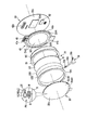
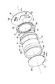
- FIG. 2 is an exploded perspective view showing components arranged in the housing of the wearable device.
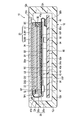
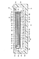
- FIG. 3 is a cross-sectional view of the wearable device taken along the line AA of FIG.
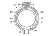
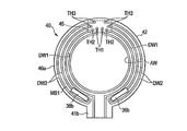
- FIG. 4 is a plan view showing the wiring side of the antenna wiring board (electronic device).
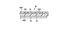
- 5 is a cross-sectional view of the antenna wiring board taken along line BB of FIG.
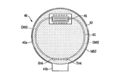
- FIG. 6 is a plan view showing the back side of the antenna wiring board.
- FIG. 7 is a plan view of the antenna wiring board according to the first modification.
- FIG. 8 is a plan view of an antenna wiring board according to a second modification.
- FIG. 9 is an exploded perspective view showing components of the wearable device according to the second embodiment.
- FIG. 10 is sectional drawing of the wearable device which concerns on 2nd Embodiment.
- FIG. 11 is a plan view of the wiring side of the antenna wiring board.
- FIG. 12 is a plan view showing the back side of the antenna wiring board.
- FIG. 13 is a plan view showing the wiring side of the antenna wiring board according to the third modification.
- FIG. 14 is a plan view showing the back side of the antenna wiring board according to the third modification.
- FIG. 15 is an exploded perspective view showing components of the wearable device according to the third embodiment.
- FIG. 16 is a cross-sectional view of the wearable device according to the third embodiment.
- FIG. 17 is a plan view showing the wiring side of the antenna wiring board according to the fourth modification.
- FIG. 18 is a cross-sectional view of the antenna wiring board taken along the line CC of FIG.
- FIG. 1 is a perspective view schematically showing a wristwatch-type wearable device according to an embodiment.
- the first embodiment shows a wearable device 10 applied to a wristwatch type.
- the wearable device 10 includes a flat circular, elliptical, or polygonal housing 12.
- a control circuit board, an antenna wiring board, a backlight device, a display panel 20 and the like, which will be described later, are housed in the housing 12 in a stacked state.
- a band 14 is attached to the housing 12.
- FIG. 2 is an exploded perspective view showing components arranged in the housing 12, and FIG. 3 is a sectional view of the wearable device 10 taken along the line AA of FIG.
- the wearable device 10 includes a display panel 20, a backlight device 30, an antenna wiring board 40, and a control circuit board 60, and these components correspond to the shape of the housing 12, It is formed in a substantially circular shape, an elliptical shape, or a polygonal shape.
- a liquid crystal display panel is used as the display panel 20.
- the display panel 20 includes a polygonal first substrate SUB1, a polygonal second substrate SUB2 arranged to face the first substrate SUB1, a first substrate SUB1 and a second substrate.
- the peripheral portion of the second substrate SUB2 is attached to the first substrate SUB1 with the sealing material SE.
- a polarizing plate (not shown) is attached to the surface of the second substrate SUB2 to form the display surface 20a of the display panel 20.
- a polarizing plate is attached to the surface of the first substrate SUB1 (the back surface of the display panel 20).
- flexible substrates formed of glass or synthetic resin sheets are used as the first substrate SUB1 and the second substrate SUB2.
- the display panel 20 includes a plurality of pixels PX arranged in a matrix in a display area.
- the first substrate SUB1 includes a source line (data bus line) S provided in the display region and extending in a first direction, and a gate line (gate bus line) G extending in a second direction orthogonal to the first direction.
- Each pixel PX includes a memory circuit (for example, SRAM) M electrically connected to the gate line G and the source line S, a voltage supply circuit VC, a pixel electrode PE connected to the voltage supply circuit VC, and the like.
- the common electrode CE having the common potential is provided on the first substrate SUB1 or the second substrate SUB2 and faces the plurality of pixel electrodes PE.
- the display panel 20 is configured as a reflective type having a reflective display function of displaying an image by selectively reflecting light from the display surface side such as external light or auxiliary light.
- each pixel electrode constitutes a reflective surface capable of reflecting external light.
- the display panel 20 has a transmissive display function of displaying an image by selectively transmitting light from a backlight device described later. At least a portion of each pixel electrode constitutes a transmissive portion that can transmit light.
- the display panel 20 may be a touch-input display panel including a touch sensor (not shown).
- the display panel 20 is not limited to the liquid crystal display panel, and an organic EL display panel can be used.
- the cover panel 24 is attached so as to overlap the display surface 20a.
- the display panel 20 is arranged in the housing 12 by supporting the peripheral portion of the cover panel 24 on the housing 12.
- the backlight device 30 as a whole is formed in a polygonal shape having substantially the same size as the display panel 20, and faces the back surface of the display panel 20 (the surface of the first substrate SUB1). Will be placed.
- the backlight device 30 includes, for example, an annular frame (bezel) 32 formed of resin, a polygonal reflection sheet RE attached to the back surface of the frame 32, and a plurality of optical members arranged in the frame 32. And a light source unit 36 that supplies light incident on the optical member.
- the optical member includes a light guide plate LG arranged on the reflection sheet RE in the frame 32, and a plurality of sheets, for example, a first optical sheet OS1 and a second optical sheet OS2 arranged on the light guide plate LG in an overlapping manner.
- the light guide plate LG is formed, for example, in a circular shape, and has a first main surface (emission surface) S1 facing the display panel 20, and a second main surface (opposite the first main surface) facing the reflection sheet RE ( It has a reflection surface) S2 and an outer peripheral surface (incident surface) EF connected to the first main surface S1a and the second main surface S2.
- the light source unit 36 includes a wiring board 36a made of a flexible printed circuit board (FPC), and two light emitting elements mounted on the wiring board 36a, for example, a light emitting diode (LED) 36b.
- the wiring board 36a is attached to the frame 32, and the LED 36b faces the incident surface EF of the light guide plate LG.
- the frame 32 of the backlight device 30 is attached to the back surface of the display panel 20 with an annular double-sided tape TP1. As a result, the backlight device 30 is arranged so as to face the back surface of the display panel 20.
- the control circuit board 60 is, for example, a circular printed circuit board 60a, a plurality of electronic components 62 such as a drive IC 62a and a connector 62b mounted on one surface of the printed circuit board 60a, and the printed circuit board 60a. And a plurality of electronic components 64 including a drive IC 64a and the like mounted on the other surface.
- the control circuit board 60 is placed on the bottom wall 12 a of the housing 12 and faces the display panel 20 and the backlight device 30. At this time, the control circuit board 60 is arranged such that the connector 62b is located on the backlight device 30 side.
- the antenna wiring board 40 which is an example of an electronic device, is arranged between the backlight device 30 and the control circuit board 60 and faces the reflection sheet RE.
- 4 is a plan view showing the first main surface side (wiring side) of the antenna wiring board 40
- FIG. 5 is a sectional view of the antenna wiring board taken along the line BB in FIG. 4, and
- FIG. It is a top view which shows the 2nd main surface side (back surface side) of a board
- the antenna wiring board 40 is composed of, for example, a flexible printed circuit board (FPC), and has a circular main body 40a, a strip-shaped first extending portion 41a extending in one direction from the peripheral edge of the main body 40a, and the peripheral edge of the main body 40a. From the first extending portion, the belt-like second extending portion 41b extending in the opposite direction is integrally provided.
- FPC flexible printed circuit board
- an antenna wiring board 40 which is an example of an electronic device, has a base layer 42 formed of an insulating material such as polyimide and a conductive layer formed on the base layer 42, such as a copper foil, patterned.
- the antenna wiring AW, the signal wiring DW1, and the second signal wiring DW2 thus formed are provided, and the protective layer 44 formed on the base layer 42 so as to overlap the conductive layer.
- the antenna wiring board 40 has a first main surface MS1 on which wiring is provided and a second main surface MS2 located opposite to the first main surface MS1.
- the antenna wiring board 40 includes the first connector 45 mounted on the first extending portion 41a on the first major surface MS1 side and the shield layer laminated on the back surface (second major surface MS2) of the base layer 42.
- the shield layer 43 is provided on the second main surface MS2 of the main body 40a and functions as a noise shield.
- the antenna wiring AW extends in a loop shape on the main body 40a, and the pair of wiring end portions extends on the first extending portion 41a and is electrically connected to the first connector 45.
- the antenna wiring AW forms a near field communication (NFC) antenna.
- the plurality of signal wirings DW1 extend from the first extension part 41a to the extension end of the second extension part 42b passing over the main body 40a.
- the signal line DW1 is arranged on the outer side and one side in the radial direction of the antenna wiring AW, and extends along the outer peripheral edge of the main body 40a.
- One ends of the plurality of signal wirings DW1 are electrically connected to the first connector 45 at the first extending portion 41a.
- the signal wiring DW1 constitutes a signal wiring for the display panel that supplies the driving signal and the driving voltage to the display panel 20. Although only two signal wirings DW1 are shown, the number of signal wirings DW1 is not limited to this and may be one or many. Further, the signal wiring DW1 is not limited to one side of the antenna wiring AW, but may be arranged on both sides of the antenna wiring. Although the antenna wiring AW is a wiring forming a near field communication (NFC) antenna, the antenna wiring AW is not limited to this and can be applied to various antennas, such as a GPS antenna GA or a Bluetooth (registered trademark) antenna. It is also possible to apply.
- NFC near field communication
- the plurality of second signal wirings DW2 extend from the first extending portion 41a to the vicinity of the second extending portion 42b passing over the main body 40a.
- the second signal line DW2 is arranged on the outer side in the radial direction of the antenna wiring AW and on the one side opposite to the signal wiring DW1 and extends along the outer peripheral edge of the main body 40a.
- One end of the second signal wiring DW2 is electrically connected to the first connector 45, respectively.
- the second connector 47 is mounted on the second main surface MS2 of the main body 40a in the vicinity of the second extending portion 41b.
- the other end of the second signal wiring DW2 is electrically connected to the second connector 47 via a conductive portion formed through the base layer 42, for example, a plated through hole TH3 or a connection terminal.
- the second connector 47 is formed so that the wiring board 36a of the light source unit 36 described above can be connected thereto.
- the antenna wiring AW side (first main surface MS1) faces the backlight device 30, and the shield layer 43 side faces the control circuit board. It is arranged so as to face 60.
- the first extending portion 41a is folded back toward the control circuit board 90 side, and the first connector 45 is electrically and mechanically joined to the connector 62b of the control circuit board 60.
- the first connector 45 is a connector that is inserted, but the present invention is not limited to this, and various connectors can be applied, for example, a ZIF type connector can also be used.
- the second extending portion 41b is joined to an end portion of the first substrate SUB1 of the display panel 20, and the signal wiring DW1 is electrically connected to the wiring of the display panel 20.
- the connection end of the wiring board 36 a of the light source unit 36 is connected to the antenna wiring board 40 via the second connector 47.
- the second connector 47 is electrically connected to the first connector 45 via the signal wiring DW3 provided on the antenna wiring board 40.
- the display panel 20 and the light source unit 36 are electrically connected to the control circuit board 60 via the signal wirings DW1 and DW2 and the first and second connectors 45 and 47 provided on the antenna wiring board 40.
- another antenna such as a GPS antenna GA or a Bluetooth antenna may be embedded and arranged in the side wall 12b of the housing 12.
- the antenna wiring board is provided by providing the antenna wiring and the signal wiring for the display panel or the light source device on the antenna wiring board.
- the display panel 20 and the light source unit 36 can be connected to the control circuit board 60. Since an independent wiring board (FPC) for connecting the display panel and an independent wiring board (FPC) for connecting the light source unit 36 are not required, the number of parts can be reduced, the manufacturing cost can be reduced, and the assemblability can be improved. Is possible.
- FPC independent wiring board
- FIG. 7 is a plan view of an antenna wiring board according to the first modification.
- the light emitting element (LED) 36b is mounted on the main body 40a of the antenna wiring board 40 in the vicinity of the second extending portion 41b.
- the antenna wiring AW, the signal wiring DW1 for the display panel, and the second signal wiring DW2 for supplying a drive signal to the LED 36b are provided on the antenna wiring board 40.
- the plurality of signal wirings DW1 extend from the first extending portion 41a to the extending end of the second extending portion 42b, passing over the main body 40a.
- the signal line DW1 is arranged on the outer side and one side in the radial direction of the antenna wiring AW, and extends along the outer peripheral edge of the main body 40a.
- the plurality of signal wirings DW1 are electrically connected to the first connector 45 at the first extending portion 41a.
- the plurality of second signal wirings DW2 extend from the first extending portion 41a to the LED 36b, passing over the main body 40a.
- the second signal line DW2 is arranged on the outer side in the radial direction of the antenna wiring AW and on the side opposite to the signal wiring DW1, and extends along the outer peripheral edge of the main body 40a.
- One ends of the second signal lines W2 are electrically connected to the LEDs 36b, respectively.
- the other end of the second signal wiring DW2 is electrically connected to the first connector 45 at the first extension 41a.
- the light source element 36b of the light source unit and the signal wiring DW2 are integrated on the antenna wiring board 40, so that the independent light source unit (wiring board and light emitting element) 36 can be omitted. .. Further, by omitting an independent wiring board (unshielded FPC) for the light source unit, it is possible to further reduce the adverse effect of noise coupling with the antenna wiring board 40.
- FIG. 8 is a plan view of an antenna wiring board according to the second modification.
- two light emitting elements (LEDs) 36b are mounted on the main body 40a of the antenna wiring board 40 in the vicinity of the second extending portion 41b.
- the antenna wiring AW, the signal wiring DW1 for the display panel, and the second signal wiring DW2 for supplying a drive signal to the LED 36b are provided.
- the plurality of signal wirings DW1 extend from the first extending portion 41a to the extending end of the second extending portion 42b passing over the main body 40a.
- the signal line DW1 is routed radially outside and on both sides of the antenna wiring AW.
- the plurality of signal wirings DW1 are electrically connected to the first connector 45 at the first extending portion 41a.
- the two second signal wirings DW2 extend from the first extending portion 41a to the one LED 36b passing over the main body 40a.
- the second signal line DW2 is arranged on the radially outer side and one side of the signal wiring DW1 and extends along the outer peripheral edge of the main body 40a.
- One ends of the second signal lines W2 are electrically connected to the LEDs 36b, respectively.
- the other end of the second signal wiring DW2 is electrically connected to the first connector 45 at the first extending portion 41a.
- the other two second signal wirings DW2 extend from the first extending portion 41a to the other LED 36b passing over the main body 40a.
- the second signal line DW2 is arranged on the outer side in the radial direction of the signal wiring DW1 and on the other side, and extends along the outer peripheral edge of the main body 40a.
- One end of the second signal line W2 is electrically connected to the other LED 36b.
- the other end of the second signal wiring DW2 is electrically connected to the first connector 45 at the first extending portion 41a. Also in the antenna wiring board according to the second modification, it is possible to obtain the same effects as those of the antenna wiring board according to the first modification described above.
- FIG. 9 is an exploded perspective view showing components of the wearable device according to the second embodiment
- FIG. 10 is a cross-sectional view of the wearable device according to the second embodiment
- FIG. 11 is wiring of an antenna wiring board.
- FIG. 12 is a plan view showing the rear side of the antenna wiring board.
- the antenna wiring board 40 is disposed between the backlight device 30 and the control circuit board 60, and the surface of the antenna wiring board 40 on the wiring side. Faces the backlight device 30, and the surface on the shield layer side faces the control circuit board 60.
- the antenna wiring board 40 integrally includes a substantially circular main body 40a and a strip-shaped second extending portion 41b extending in one direction from the outer peripheral edge of the main body 40a. There is.
- the first extending portion is not provided.
- Two light emitting elements (LEDs) 36b are mounted on the main body 40a of the antenna wiring board 40 in the vicinity of the second extending portion 41b.
- the antenna wiring AW, the signal wiring DW1 for the display panel, and the second signal wiring DW2 for supplying a drive signal to the LED 36b are provided on the antenna wiring board 40.
- the first connector 45 is mounted on the back surface (second main surface S2) of the antenna wiring board 40. Further, the shield layer 43 is laminated on the entire back surface of the main body 40a except the first connector 45.
- the antenna wiring AW extends in a loop shape on the main body 40a, and a pair of end portions of the antenna wiring AW are arranged at one end portion of the main body 40a, here, at an end portion opposite to the second extending portion 41b. ing. These end portions are electrically connected to the rear-side first connector 45 through a conductive portion provided through the base layer 42, for example, a plated through hole TH1 or a connection terminal.
- Each of the plurality of signal wirings DW1 extends from the one end of the main body 40a to the extending end of the second extending portion 42b.
- the signal line DW1 is routed radially outside and on both sides of the antenna wiring AW.
- One end of each signal wiring DW1 is electrically connected to the first connector 45 via a conductive portion provided through the base layer 42, for example, a plated through hole TH2 or a connection terminal.
- the two second signal wirings DW2 extend from the one end of the main body 40a to the LED 36b on the main body 40a.
- the second signal line DW2 is arranged on the radially outer side and one side of the signal wiring DW1 and extends along the outer peripheral edge of the main body 40a.
- the extended ends of the second signal lines W2 are electrically connected to the LEDs 36b, respectively.
- one end of the second signal wiring DW2 is electrically connected to the first connector 45 on the back surface side through the plated through hole TH3 or the connection terminal.
- the other two second signal wirings DW2 extend from the one end of the main body 40a to the other LED 36b passing over the main body 40a.
- the second signal line DW2 is arranged on the outer side in the radial direction of the signal wiring DW1 and on the other side, and extends along the outer peripheral edge of the main body 40a.
- the extended ends of the second signal lines W2 are electrically connected to the other LEDs 36b.
- the second signal wiring DW2 is electrically connected to the first connector 45 via the plated through hole TH3 or the connection terminal.
- the antenna wiring board 40 is arranged such that the wiring side surface faces the reflection sheet RE.
- the first connector 45 of the antenna wiring board 40 is fitted to the second connector 62b of the control circuit board 60.
- the first connector 45 and the second connector 62b are stacking connectors that can be fitted to each other, or so-called BtoB connectors.
- the antenna wiring AW, the signal wiring DW1, and the second signal wiring DW2 of the antenna wiring board 40 are electrically connected to the control circuit board 60 via the first connector 45 and the second connector 62b.
- the second extending portion 41b of the antenna wiring board 40 is joined to the end portion of the first substrate SUB1 of the display panel 20.
- the signal wiring DW1 is electrically connected to the wiring of the first substrate SUB1.
- the LED 36b mounted on the antenna wiring board 40 is positioned adjacent to and facing the entrance surface EF of the light guide plate LG.
- the display panel 20 and the LEDs 36b can be connected to the control circuit board 60 via the antenna wiring board. Since an independent wiring board (FPC) for connecting the display panel and an independent wiring board (FPC) for connecting the light source unit 36 are not required, the number of parts can be reduced, the manufacturing cost can be reduced, and the assemblability can be improved. Is possible.
- FPC independent wiring board
- the FPC even when the FPC is arranged in a small housing, it is not necessary to stack another FPC on the antenna wiring board 40 (stacking in a direction orthogonal to the board surface), and the cross between the antenna wiring AW and the FPC is not necessary. Generation of noise due to talk and adverse effects on other antennas can be significantly reduced and suppressed. Further, by mounting the light emitting element (LED) 36b on the antenna wiring board 40, an independent light source device (wiring board and light emitting element) is not required, and the number of parts and the size of the device can be reduced.
- LED light emitting element
- the stacking connector provided on the back surface of the main body 40a is used as the first connector of the antenna wiring board 40, so that the first extension portion 41a of the antenna wiring board 40 is omitted and the antenna wiring board It is possible to reduce the size of 40. At the same time, the antenna wiring board 40 and the control circuit board 60 can be easily connected. From the above, according to the second embodiment, an electronic device capable of reducing noise interference with the antenna and other electronic components can be obtained.
- FIG. 13 is a plan view showing the wiring side of the antenna wiring board according to the third modified example
- FIG. 14 is a plan view showing the back side of the antenna wiring board.
- two light emitting elements (LEDs) 36b are mounted on the main body 40a of the antenna wiring board 40 in the vicinity of the second extending portion 41b.
- a second signal wiring DW2 for supplying a drive signal to the LED 36b is provided on the antenna wiring board 40.
- Each of the two second signal wirings DW2 extends from one end of the main body 40a to the one LED 36b passing over the main body 40a and electrically connected to the LED 36b.
- One end of the second signal wiring DW2 is electrically connected to the rear-side first connector 45 via a plated through hole TH3 or a connection terminal.
- the other end of the second signal wiring DW2 extends from the LED 36b and is exposed on the back surface of the antenna wiring board 40 through the plated through hole TH4 or the connection terminal, and further on the back surface side of the antenna wiring board 40. It extends through the (connector mounting surface) to the first connector 45 and is electrically connected to the first connector 45.
- Other configurations of the antenna wiring board are the same as those of the antenna wiring board in the second embodiment described above.
- FIG. 15 is an exploded perspective view showing components of the wearable device according to the third embodiment
- FIG. 16 is a sectional view of the wearable device according to the third embodiment.
- the antenna wiring board 40 is arranged between the backlight device 30 and the control circuit board 60, and the surface of the antenna wiring board 40 on the wiring side. Faces the backlight device 30, and the surface on the shield layer side faces the control circuit board 60.
- the antenna wiring board 40 has a white cover layer RE formed on the entire surface of the main body 40a except the LEDs 36b.
- the white cover layer RE functions as a reflection sheet of the backlight device 30.
- the white cover layer RE is located adjacent to and opposed to the back surface S2 of the light guide plate LG, and reflects the light emitted from the light guide plate LG toward the light guide plate LG.
- the reflection sheet of the backlight device 30 is omitted, and the reflection sheet is integrated with the antenna wiring board 40.
- Other configurations of the wearable device 10 are the same as those of the wearable device according to the second embodiment described above.
- the third embodiment by providing the antenna wiring board 40 with the function of the reflection sheet, various functions can be integrated in the antenna wiring board 40, and the number of constituent parts of the wearable device can be reduced. It is possible to plan.
- FIG. 17 is a plan view showing the antenna wiring board of the wearable device according to the fourth embodiment
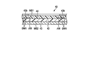
- FIG. 18 is a sectional view of the antenna wiring board taken along the line CC in FIG.
- the antenna wiring board 40 is provided on the wiring side surface of the main body 40a in addition to the shield layer 43 formed on the back surface of the main body 40a.
- the second shield layer 43b is provided.
- the second shield layer 43b is formed in an annular shape and has an outer diameter substantially equal to that of the main body 40a and an inner diameter slightly larger than the diameter of the antenna wiring AW.
- the second shield layer 43b covers the signal wiring DW1 except for the antenna wiring AW and the LED 36b.
- the other configurations of the antenna wiring board 40 and the wearable device are the same as those of the antenna wiring board according to the second embodiment described above.
- the fourth embodiment by providing the second shield layer 43b on the antenna wiring board 40, noise due to crosstalk between the signal wiring DW1 and other electronic components and adverse effects on other antennas are prevented. It can be further reduced and suppressed.
- the fourth embodiment it is possible to obtain the same operational effects as those of the above-described first and second embodiments.
- the antenna wiring board is not limited to a circular shape, and can have any shape according to the shape of the housing or the installation place.
- the number of signal wirings is not limited to the embodiment and can be increased or decreased as necessary.
- the number of light sources installed is not limited to one or two, and may be increased as necessary.
- the wearable device is not limited to the wristwatch type, and can be applied to various other wearable devices.
- the display panel is not limited to the liquid crystal display panel with a built-in memory, and other liquid crystal display panel or organic EL display panel may be used.
Landscapes
- Physics & Mathematics (AREA)
- General Physics & Mathematics (AREA)
- Engineering & Computer Science (AREA)
- Microelectronics & Electronic Packaging (AREA)
- Signal Processing (AREA)
- Computer Networks & Wireless Communication (AREA)
- Electromagnetism (AREA)
- Support Of Aerials (AREA)
- Structure Of Printed Boards (AREA)
- Electric Clocks (AREA)
- Shielding Devices Or Components To Electric Or Magnetic Fields (AREA)
- Details Of Aerials (AREA)
- Transceivers (AREA)
Abstract
実施形態に係る電子機器は、表示パネルと、表示パネルに重ねて配置され、アンテナを形成したアンテナ配線AWを有するアンテナ配線基板40と、アンテナ配線基板に形成され表示パネルに駆動信号を供給する信号配線DWと、を備えている。
Description
本発明の実施形態は、アンテナ配線基板を有する電子機器に関する。
近年、スマートフォン等のモバイル電子機器、身体に装着可能なウエラブル電子機器が多数提供されている。これらのモバイル電子機器、ウエラブル電子機器は、通常、無線通信可能な無線アンテナ、表示パネル(液晶表示パネル、有機EL表示パネル)、プリント回路基板等を備えて構成されている。
電子回路や電子部品には、長波長帯域のノイズを発生するものが多く、標準電波を受信する際に隣接する配線や電子部品からのノイズが混入しやすい。また、例えば、腕時計のような小型のウエラブル電子機器では、筐体あるいはケース内に、無線アンテナ、表示パネルの配線、バックライト装置の配線、他の電子部品が密に配置されている。そのため、ノイズ混入に係る問題が顕著となる。例えば、配線間のカップリングに起因するノイズの発生、および電子部品から配線へのノイズの混入が発生しやすい。
電子回路や電子部品には、長波長帯域のノイズを発生するものが多く、標準電波を受信する際に隣接する配線や電子部品からのノイズが混入しやすい。また、例えば、腕時計のような小型のウエラブル電子機器では、筐体あるいはケース内に、無線アンテナ、表示パネルの配線、バックライト装置の配線、他の電子部品が密に配置されている。そのため、ノイズ混入に係る問題が顕著となる。例えば、配線間のカップリングに起因するノイズの発生、および電子部品から配線へのノイズの混入が発生しやすい。
この発明の実施形態の課題は、アンテナおよび他の電子部品とのノイズ干渉を低減することが可能な電子機器を提供することにある。
実施形態に係る電子機器は、表示パネルと、前記表示パネルと重ねて配置され、アンテナを形成するアンテナ配線を有するアンテナ配線基板と、前記アンテナ配線基板に設けられ、前記表示パネルに駆動信号を供給する信号配線と、を備えている。
以下、図面を参照しながら、この発明の実施形態について詳細に説明する。
なお、開示はあくまで一例にすぎず、当業者において、発明の主旨を保っての適宜変更であって容易に想到し得るものについては、当然に本発明の範囲に含有されるものである。また、図面は説明をより明確にするため、実際の態様に比べ、各部の幅、厚さ、形状等について模式的に表される場合があるが、あくまで一例であって、本発明の解釈を限定するものではない。また、本明細書と各図において、既出の図に関して前述したものと同様の要素には、同一の符号を付して、詳細な説明を適宜省略することがある。
なお、開示はあくまで一例にすぎず、当業者において、発明の主旨を保っての適宜変更であって容易に想到し得るものについては、当然に本発明の範囲に含有されるものである。また、図面は説明をより明確にするため、実際の態様に比べ、各部の幅、厚さ、形状等について模式的に表される場合があるが、あくまで一例であって、本発明の解釈を限定するものではない。また、本明細書と各図において、既出の図に関して前述したものと同様の要素には、同一の符号を付して、詳細な説明を適宜省略することがある。
(第1の実施形態)
図1は、実施形態に係る腕時計型のウエラブルデバイスを概略的に示す斜視図である。第1の実施形態は、腕時計型に適用したウエラブルデバイス10を示している。図示のように、ウエラブルデバイス10は、偏平な円形、楕円形、あるいは、多角形状の筐体12を備えている。筐体12内には、後述する制御回路基板、アンテナ配線基板、バックライト装置、表示パネル20等が積層状態で収納されている。また、筐体12にはバンド14が取り付けられている。
図1は、実施形態に係る腕時計型のウエラブルデバイスを概略的に示す斜視図である。第1の実施形態は、腕時計型に適用したウエラブルデバイス10を示している。図示のように、ウエラブルデバイス10は、偏平な円形、楕円形、あるいは、多角形状の筐体12を備えている。筐体12内には、後述する制御回路基板、アンテナ配線基板、バックライト装置、表示パネル20等が積層状態で収納されている。また、筐体12にはバンド14が取り付けられている。
図2は、筐体12内に配置される構成要素を示す分解斜視図、図3は、図1の線A-Aに沿ったウエラブルデバイス10の断面図である。
図2に示すように、ウエラブルデバイス10は、表示パネル20、バックライト装置30、アンテナ配線基板40、および制御回路基板60を備え、これらの構成要素は、筐体12の形状に合わせて、ほぼ円形、楕円形、あるいは多角形状に形成されている。
一例では、表示パネル20として液晶表示パネルを用いている。図2および図3に示すように、表示パネル20は、多角形状の第1基板SUB1と、第1基板SUB1に対向配置された多角形の第2基板SUB2と、第1基板SUB1と第2基板SUB2との間に封止された液晶層LCと、を備えている。第2基板SUB2の周縁部は、シール材SEにより第1基板SUB1に貼り合わされている。第2基板SUB2の表面に図示しない偏光板が貼付され、表示パネル20の表示面20aを形成している。第1基板SUB1の表面(表示パネル20の背面)に偏光板が貼付されている。第1基板SUB1および第2基板SUB2は、それぞれガラスあるいは合成樹脂シートで形成された可撓性基板を用いている。
図2に示すように、ウエラブルデバイス10は、表示パネル20、バックライト装置30、アンテナ配線基板40、および制御回路基板60を備え、これらの構成要素は、筐体12の形状に合わせて、ほぼ円形、楕円形、あるいは多角形状に形成されている。
一例では、表示パネル20として液晶表示パネルを用いている。図2および図3に示すように、表示パネル20は、多角形状の第1基板SUB1と、第1基板SUB1に対向配置された多角形の第2基板SUB2と、第1基板SUB1と第2基板SUB2との間に封止された液晶層LCと、を備えている。第2基板SUB2の周縁部は、シール材SEにより第1基板SUB1に貼り合わされている。第2基板SUB2の表面に図示しない偏光板が貼付され、表示パネル20の表示面20aを形成している。第1基板SUB1の表面(表示パネル20の背面)に偏光板が貼付されている。第1基板SUB1および第2基板SUB2は、それぞれガラスあるいは合成樹脂シートで形成された可撓性基板を用いている。
図2に模式的に示すように、表示パネル20は、表示領域にマトリクス状に配列された複数の画素PXを備えている。第1基板SUB1は、表示領域に設けられ第1方向に延出するソース線(データバスライン)Sと、第1方向と直交する第2方向に延出するゲート線(ゲートバスライン)Gとを有している。各画素PXは、ゲート線Gおよびソース線Sと電気的に接続されたメモリ回路(例えば、SRAM)Mおよび電圧供給回路VC、電圧供給回路VCに接続された画素電極PEなどを備えている。コモン電位の共通電極CEは、第1基板SUB1または第2基板SUB2に備えられ、複数の画素電極PEと対向している。
表示パネル20は、外光や補助光といった表示面側からの光を選択的に反射させることで画像を表示する反射表示機能を備えた反射型として構成されている。一例では、各画素電極の少なくとも一部は、外光を反射可能な反射面を構成している。また、本実施形態において、表示パネル20は、後述するバックライト装置からの光を選択的に透過させることで画像を表示する透過表示機能を備えている。各画素電極の少なくとも一部は、光を透過可能な透過部を構成している。表示パネル20は、図示しないタッチセンサを備えたタッチ入力可能な表示パネルとしてもよい。表示パネル20は、液晶表示パネルに限らず、有機EL表示パネルを用いることも可能である。
本実施形態では、表示面20aに重ねてカバーパネル24が貼付されている。表示パネル20は、カバーパネル24の周縁部を筐体12に支持することにより、筐体12内に配置されている。
本実施形態では、表示面20aに重ねてカバーパネル24が貼付されている。表示パネル20は、カバーパネル24の周縁部を筐体12に支持することにより、筐体12内に配置されている。
図2および図3に示したように、バックライト装置30は、全体として、表示パネル20とほぼ等しい大きさの多角形状に構成され、表示パネル20の背面(第1基板SUB1の表面)に対向して配置される。バックライト装置30は、例えば樹脂で形成された環状のフレーム(ベゼル)32と、フレーム32の背面に貼付された多角形の反射シートREと、フレーム32内に配置された複数の光学部材と、光学部材に入射する光を供給する光源ユニット36と、を備えている。
光学部材は、フレーム32内で反射シートRE上に配置された導光板LG、および導光板LG上に重ねて配置された複数枚、例えば、第1光学シートOS1、第2光学シートOS2を有している。導光板LGは、例えば、円形に形成され、表示パネル20に対向する第1主面(出射面)S1、この第1主面と反対側に位置し反射シートREに対向する第2主面(反射面)S2、および、第1主面S1aと第2主面S2とに繋がる外周面(入射面)EFを有している。
光学部材は、フレーム32内で反射シートRE上に配置された導光板LG、および導光板LG上に重ねて配置された複数枚、例えば、第1光学シートOS1、第2光学シートOS2を有している。導光板LGは、例えば、円形に形成され、表示パネル20に対向する第1主面(出射面)S1、この第1主面と反対側に位置し反射シートREに対向する第2主面(反射面)S2、および、第1主面S1aと第2主面S2とに繋がる外周面(入射面)EFを有している。
光源ユニット36は、フレキシブルプリント回路基板(FPC)からなる配線基板36aと、配線基板36a上に実装された2つの発光素子、例えば、発光ダイオード(LED)36bと、を有している。配線基板36aはフレーム32に取付けられ、LED36bは導光板LGの入射面EFに対向している。
バックライト装置30のフレーム32は、環状の両面テープTP1により表示パネル20の背面に貼付される。これにより、バックライト装置30は、表示パネル20の背面に対向した状態に配置されている。
バックライト装置30のフレーム32は、環状の両面テープTP1により表示パネル20の背面に貼付される。これにより、バックライト装置30は、表示パネル20の背面に対向した状態に配置されている。
制御回路基板60は、一例では円形に形成されたプリント回路基板60aと、プリント回路基板60aの一方の表面に実装された駆動IC62a、コネクタ62b等の複数の電子部品62と、プリント回路基板60aの他方の表面に実装された駆動IC64a等を含む複数の電子部品64と、を有している。制御回路基板60は、筐体12の底壁12a上に載置され、表示パネル20およびバックライト装置30と対向している。この際、制御回路基板60は、コネクタ62bがバックライト装置30側に位置するように配置される。
電子機器の一例であるアンテナ配線基板40は、バックライト装置30と制御回路基板60との間に配置され、反射シートREに対向している。図4は、アンテナ配線基板40の第1主面側(配線側)を示す平面図、図5は、図4の線B-Bに沿ったアンテナ配線基板の断面図、図6は、アンテナ配線基板の第2主面側(背面側)を示す平面図である。
アンテナ配線基板40は、例えば、フレキシブルプリント回路基板(FPC)で構成され、円形の本体40aと、本体40aの周縁から一方向に延出した帯状の第1延出部41aと、本体40aの周縁から第1延出部と反対の方向に延出した帯状の第2延出部41bとを一体に有している。
アンテナ配線基板40は、例えば、フレキシブルプリント回路基板(FPC)で構成され、円形の本体40aと、本体40aの周縁から一方向に延出した帯状の第1延出部41aと、本体40aの周縁から第1延出部と反対の方向に延出した帯状の第2延出部41bとを一体に有している。
図示のように、電子機器の一例であるアンテナ配線基板40は、ポリイミド等の絶縁材料で形成されたベース層42と、ベース層42上に形成された導電層、例えば、銅箔、をパターニングすることにより形成されたアンテナ配線AW、信号配線DW1、および第2信号配線DW2と、導電層に重ねてベース層42上に形成された保護層44と、を有している。アンテナ配線基板40は、配線が設けられている第1主面MS1と、第1主面MS1の反対側に対向して位置する第2主面MS2と、を有している。また、アンテナ配線基板40は、第1主面MS1側で第1延出部41a上に実装された第1コネクタ45と、ベース層42の背面(第2主面MS2)に積層されたシールド層43とを有している。本実施形態において、シールド層43は、本体40aの第2主面MS2に設けられ、ノイズシールドとして機能する。
アンテナ配線AWは、本体40a上にループ状に延在し、一対の配線端部は第1延出部41a上に延在し第1コネクタ45に電気的に接続されている。アンテナ配線AWは、近距離無線通信(NFC)アンテナを形成している。
一例では、複数の信号配線DW1は、第1延出部41aから本体40a上を通り第2延出部42bの延出端まで延在している。本体40a上において、信号線DW1は、アンテナ配線AWの径方向外側、かつ、片側に配置され、本体40aの外周縁に沿って延在している。複数の信号配線DW1の一端部は、第1延出部41aにおいて第1コネクタ45に電気的に接続されている。第1の実施形態において、信号配線DW1は、表示パネル20へ駆動信号および駆動電圧を供給する表示パネル用の信号配線を構成している。信号配線DW1は2本のみ図示しているが、これに限らず、一本あるいは3本以上の多数本としてもよい。また、信号配線DW1は、アンテナ配線AWの片側に限らず、アンテナ配線の両側にそれぞれ配置する構成としてもよい。
なお、アンテナ配線AWは、近距離無線通信(NFC)アンテナを形成する配線としているが、これに限らず、種々のアンテナに適用可能であり、GPSアンテナGAあるいはブルートゥース(登録商標)用アンテナ等に適用することも可能である。
一例では、複数の信号配線DW1は、第1延出部41aから本体40a上を通り第2延出部42bの延出端まで延在している。本体40a上において、信号線DW1は、アンテナ配線AWの径方向外側、かつ、片側に配置され、本体40aの外周縁に沿って延在している。複数の信号配線DW1の一端部は、第1延出部41aにおいて第1コネクタ45に電気的に接続されている。第1の実施形態において、信号配線DW1は、表示パネル20へ駆動信号および駆動電圧を供給する表示パネル用の信号配線を構成している。信号配線DW1は2本のみ図示しているが、これに限らず、一本あるいは3本以上の多数本としてもよい。また、信号配線DW1は、アンテナ配線AWの片側に限らず、アンテナ配線の両側にそれぞれ配置する構成としてもよい。
なお、アンテナ配線AWは、近距離無線通信(NFC)アンテナを形成する配線としているが、これに限らず、種々のアンテナに適用可能であり、GPSアンテナGAあるいはブルートゥース(登録商標)用アンテナ等に適用することも可能である。
複数の第2信号配線DW2は、第1延出部41aから本体40a上を通り第2延出部42bの近傍まで延在している。本体40a上において、第2信号線DW2は、アンテナ配線AWの径方向外側、かつ、信号配線DW1と反対の片側に配置され、本体40aの外周縁に沿って延在している。第2信号配線DW2の一端部はそれぞれ第1コネクタ45に電気的に接続されている。また、第2延出部41bの近傍で、本体40aの第2主面MS2に第2コネクタ47が実装されている。第2信号配線DW2の他端部は、ベース層42に貫通形成された導電部、例えば、メッキスルーホールTH3あるいは接続端子を介して、第2コネクタ47に電気的に接続されている。なお、第2コネクタ47は、前述した光源ユニット36の配線基板36aを接続可能に形成されている。
図2および図3に示すように、上記のように構成されたアンテナ配線基板40は、アンテナ配線AW側(第1主面MS1)がバックライト装置30に対向し、シールド層43側が制御回路基板60と対向した状態で配置されている。第1延出部41aは、制御回路基板90側に折り返され、第1コネクタ45は制御回路基板60のコネクタ62bに電気的、かつ、機械的に接合されている。本実施形態において、第1コネクタ45は、差し込み方のコネクタを用いているが、これに限らず、種々のコネクタを適用可能であり、例えば、ZIFタイプのコネクタを使用することも可能である。
第2延出部41bは、表示パネル20の第1基板SUB1の端部に接合され、信号配線DW1は、表示パネル20の配線に電気的に接続されている。光源ユニット36の配線基板36aの接続端部は、第2コネクタ47を介してアンテナ配線基板40に接続されている。第2コネクタ47は、アンテナ配線基板40に設けられた信号配線DW3を介して第1コネクタ45に電気的に接続されている。
以上のように、表示パネル20および光源ユニット36は、アンテナ配線基板40に設けられた信号配線DW1、DW2および第1および第2コネクタ45、47を介して、制御回路基板60に電気的に接続されている。
なお、図3に示すように、筐体12の側壁12bにGPSアンテナGAあるいはブルートゥース用アンテナ等の他のアンテナを埋め込んで配置してもよい。
第2延出部41bは、表示パネル20の第1基板SUB1の端部に接合され、信号配線DW1は、表示パネル20の配線に電気的に接続されている。光源ユニット36の配線基板36aの接続端部は、第2コネクタ47を介してアンテナ配線基板40に接続されている。第2コネクタ47は、アンテナ配線基板40に設けられた信号配線DW3を介して第1コネクタ45に電気的に接続されている。
以上のように、表示パネル20および光源ユニット36は、アンテナ配線基板40に設けられた信号配線DW1、DW2および第1および第2コネクタ45、47を介して、制御回路基板60に電気的に接続されている。
なお、図3に示すように、筐体12の側壁12bにGPSアンテナGAあるいはブルートゥース用アンテナ等の他のアンテナを埋め込んで配置してもよい。
以上のように構成された第1の実施形態に係るウエラブルデバイス10によれば、アンテナ配線基板上にアンテナ配線および表示パネル用あるいは光源装置用の信号配線を設けることにより、このアンテナ配線基板を介して、表示パネル20および光源ユニット36を制御回路基板60に接続することが可能となる。表示パネル接続用の独立した配線基板(FPC)、および、光源ユニット36接続用の独立した配線基板(FPC)が不要となり、部品点数の削減、製造コストの低減、組立性の向上、を図ることが可能となる。同時に、小型の筐体内に配置した場合でも、他のFPCをアンテナ配線基板40に重ねて(基板表面と直交する方向に重ねて)配置する必要がなく、アンテナ配線AWとFPCとの間のクロストークによるノイズの発生および他のアンテナへの悪影響を大幅に低減、抑制することができる。更に、部品点数を削減することにより、ウエラブルデバイスの構成要素を小型の筐体内に容易に設置することが可能となり、あるいは、筐体の一層の小型化を図ることが可能となる。以上のことから、第1の実施形態によれば、アンテナおよび他の電子部品とのノイズ干渉を低減することが可能な電子機器が得られる。
次に、変形例に係るアンテナ配線基板および他の実施形態係るウエラブルデバイスについて説明する。以下に説明する変形例および他の実施形態において、前述した第1の実施形態と同一の部分には、同一の参照符号を付してその詳細な説明を省略あるいは簡略化し、第1の実施形態と異なる部分を中心に詳しく説明する。
(第1変形例)
図7は、第1変形例に係るアンテナ配線基板の平面図である。
図7に示すように、第1変形例では、アンテナ配線基板40の本体40a上で第2延出部41bの近傍に、発光素子(LED)36bが実装されている。アンテナ配線基板40上に、アンテナ配線AW、表示パネル用の信号配線DW1、更に、LED36bに駆動信号を供給するための第2信号配線DW2が設けられている。
複数の信号配線DW1は、第1延出部41aから本体40a上を通り第2延出部42bの延出端まで延在している。本体40a上において、信号線DW1は、アンテナ配線AWの径方向外側、かつ、片側に配置され、本体40aの外周縁に沿って延在している。複数の信号配線DW1は、第1延出部41aにおいて第1コネクタ45に電気的に接続されている。
図7は、第1変形例に係るアンテナ配線基板の平面図である。
図7に示すように、第1変形例では、アンテナ配線基板40の本体40a上で第2延出部41bの近傍に、発光素子(LED)36bが実装されている。アンテナ配線基板40上に、アンテナ配線AW、表示パネル用の信号配線DW1、更に、LED36bに駆動信号を供給するための第2信号配線DW2が設けられている。
複数の信号配線DW1は、第1延出部41aから本体40a上を通り第2延出部42bの延出端まで延在している。本体40a上において、信号線DW1は、アンテナ配線AWの径方向外側、かつ、片側に配置され、本体40aの外周縁に沿って延在している。複数の信号配線DW1は、第1延出部41aにおいて第1コネクタ45に電気的に接続されている。
複数の第2信号配線DW2は、第1延出部41aから本体40a上を通りLED36bまで延在している。本体40a上において、第2信号線DW2は、アンテナ配線AWの径方向外側、かつ、信号配線DW1と反対側に配置され、本体40aの外周縁に沿って延在している。第2信号線W2の一端部は、それぞれLED36bに電気的に接続されている。また、第2信号配線DW2の他端部は、第1延出部41aにおいて第1コネクタ45に電気的に接続されている。
上記第1変形例によれば、アンテナ配線基板40上に、光源ユニットの発光素子36bおよび信号配線DW2を集約することにより、独立した光源ユニット(配線基板および発光素子)36を省略することができる。また、光源ユニット用の独立した配線基板(シールドされていないFPC)を省略することにより、アンテナ配線基板40とのノイズカップリングによる悪影響を一層低減することが可能となる。
(第2変形例)
図8は、第2変形例に係るアンテナ配線基板の平面図である。
図8に示すように、第2変形例では、アンテナ配線基板40の本体40a上で第2延出部41bの近傍に、2つの発光素子(LED)36bが実装されている。アンテナ配線基板40上に、アンテナ配線AW、表示パネル用の信号配線DW1、更に、LED36bに駆動信号を供給するための第2信号配線DW2が設けられている。
第2変形例において、複数の信号配線DW1は、第1延出部41aから本体40a上を通り第2延出部42bの延出端まで延在している。本体40a上において、信号線DW1は、アンテナ配線AWの径方向外側、かつ、両側に引き回されている。複数の信号配線DW1は、第1延出部41aにおいて第1コネクタ45に電気的に接続されている。
図8は、第2変形例に係るアンテナ配線基板の平面図である。
図8に示すように、第2変形例では、アンテナ配線基板40の本体40a上で第2延出部41bの近傍に、2つの発光素子(LED)36bが実装されている。アンテナ配線基板40上に、アンテナ配線AW、表示パネル用の信号配線DW1、更に、LED36bに駆動信号を供給するための第2信号配線DW2が設けられている。
第2変形例において、複数の信号配線DW1は、第1延出部41aから本体40a上を通り第2延出部42bの延出端まで延在している。本体40a上において、信号線DW1は、アンテナ配線AWの径方向外側、かつ、両側に引き回されている。複数の信号配線DW1は、第1延出部41aにおいて第1コネクタ45に電気的に接続されている。
2本の第2信号配線DW2は、第1延出部41aから本体40a上を通り一方のLED36bまで延在している。本体40a上において、第2信号線DW2は、信号配線DW1の径方向外側、かつ、片側に配置され、本体40aの外周縁に沿って延在している。第2信号線W2の一端部は、それぞれLED36bに電気的に接続されている。また、第2信号配線DW2の他端部は、第1延出部41aにおいて第1コネクタ45に電気的に接続されている。
他の2本の第2信号配線DW2は、第1延出部41aから本体40a上を通り他方のLED36bまで延在している。本体40a上において、第2信号線DW2は、信号配線DW1の径方向外側、かつ、他方の片側に配置され、本体40aの外周縁に沿って延在している。第2信号線W2の一端部は、それぞれ他方のLED36bに電気的に接続されている。また、第2信号配線DW2の他端部は、第1延出部41aにおいて第1コネクタ45に電気的に接続されている。
第2変形例に係るアンテナ配線基板においても、上述した第1変形例に係るアンテナ配線基板と同様の作用効果を得ることができる。
他の2本の第2信号配線DW2は、第1延出部41aから本体40a上を通り他方のLED36bまで延在している。本体40a上において、第2信号線DW2は、信号配線DW1の径方向外側、かつ、他方の片側に配置され、本体40aの外周縁に沿って延在している。第2信号線W2の一端部は、それぞれ他方のLED36bに電気的に接続されている。また、第2信号配線DW2の他端部は、第1延出部41aにおいて第1コネクタ45に電気的に接続されている。
第2変形例に係るアンテナ配線基板においても、上述した第1変形例に係るアンテナ配線基板と同様の作用効果を得ることができる。
(第2の実施形態)
図9は、第2の実施形態に係るウエラブルデバイスの構成要素を示す分解斜視図、図10は、第2の実施形態に係るウエラブルデバイスの断面図、図11は、アンテナ配線基板の配線側を示す平面図、図12は、前記アンテナ配線基板の背面側を示す平面図である。
第2の実施形態によれば、図9および図10に示すように、アンテナ配線基板40は、バックライト装置30と制御回路基板60との間に配置され、アンテナ配線基板40の配線側の面がバックライト装置30に対向し、シールド層側の面が制御回路基板60に対向している。
図9は、第2の実施形態に係るウエラブルデバイスの構成要素を示す分解斜視図、図10は、第2の実施形態に係るウエラブルデバイスの断面図、図11は、アンテナ配線基板の配線側を示す平面図、図12は、前記アンテナ配線基板の背面側を示す平面図である。
第2の実施形態によれば、図9および図10に示すように、アンテナ配線基板40は、バックライト装置30と制御回路基板60との間に配置され、アンテナ配線基板40の配線側の面がバックライト装置30に対向し、シールド層側の面が制御回路基板60に対向している。
図11および図12に示すように、アンテナ配線基板40は、ほぼ円形の本体40aと、本体40aの外周縁から一方向に延出した帯状の第2延出部41bとを一体に有している。第1延出部は設けられていない。アンテナ配線基板40の本体40a上で第2延出部41bの近傍に、2つの発光素子(LED)36bが実装されている。アンテナ配線基板40上に、アンテナ配線AW、表示パネル用の信号配線DW1、更に、LED36bに駆動信号を供給するための第2信号配線DW2が設けられている。アンテナ配線基板40の背面(第2主面S2)に第1コネクタ45が実装されている。更に、第1コネクタ45を除く本体40aの背面全体にシールド層43が積層されている。
アンテナ配線AWは、本体40a上にループ状に延在し、アンテナ配線AWの一対の端部は、本体40aの一端部、ここでは、第2延出部41bと反対側の端部に配置されている。これらの端部は、ベース層42を貫通して設けられた導電部、例えば、メッキスルーホールTH1あるいは接続端子を介して、背面側の第1コネクタ45に電気的に接続されている。
複数の信号配線DW1は、それぞれ本体40aの上記一端部から第2延出部42bの延出端まで延在している。本体40a上において、信号線DW1は、アンテナ配線AWの径方向外側、かつ、両側に引き回されている。各信号配線DW1の一端部は、ベース層42を貫通して設けられた導電部、例えば、メッキスルーホールTH2あるいは接続端子を介して、第1コネクタ45に電気的に接続されている。
複数の信号配線DW1は、それぞれ本体40aの上記一端部から第2延出部42bの延出端まで延在している。本体40a上において、信号線DW1は、アンテナ配線AWの径方向外側、かつ、両側に引き回されている。各信号配線DW1の一端部は、ベース層42を貫通して設けられた導電部、例えば、メッキスルーホールTH2あるいは接続端子を介して、第1コネクタ45に電気的に接続されている。
2本の第2信号配線DW2は、それぞれ本体40aの上記一端部から本体40a上を通り一方のLED36bまで延在している。本体40a上において、第2信号線DW2は、信号配線DW1の径方向外側、かつ、片側に配置され、本体40aの外周縁に沿って延在している。第2信号線W2の延出端は、それぞれLED36bに電気的に接続されている。また、第2信号配線DW2の一端は、メッキスルーホールTH3あるいは接続端子を介して、背面側の第1コネクタ45に電気的に接続されている。
他の2本の第2信号配線DW2は、それぞれ本体40aの上記一端部から本体40a上を通り他方のLED36bまで延在している。本体40a上において、第2信号線DW2は、信号配線DW1の径方向外側、かつ、他方の片側に配置され、本体40aの外周縁に沿って延在している。第2信号線W2の延出端は、それぞれ他方のLED36bに電気的に接続されている。また、第2信号配線DW2は、メッキスルーホールTH3あるいは接続端子を介して、第1コネクタ45に電気的に接続されている。
他の2本の第2信号配線DW2は、それぞれ本体40aの上記一端部から本体40a上を通り他方のLED36bまで延在している。本体40a上において、第2信号線DW2は、信号配線DW1の径方向外側、かつ、他方の片側に配置され、本体40aの外周縁に沿って延在している。第2信号線W2の延出端は、それぞれ他方のLED36bに電気的に接続されている。また、第2信号配線DW2は、メッキスルーホールTH3あるいは接続端子を介して、第1コネクタ45に電気的に接続されている。
図10に示すように、アンテナ配線基板40は、配線側の面が反射シートREに対向して配置されている。アンテナ配線基板40の第1コネクタ45は、制御回路基板60の第2コネクタ62bに嵌合している。第1コネクタ45および第2コネクタ62bは、互いに嵌合可能なスタッキングコネクタあるいは、いわゆるBtoBコネクタで構成されている。これにより、アンテナ配線基板40のアンテナ配線AW、信号配線DW1、および第2信号配線DW2は、第1コネクタ45および第2コネクタ62bを介して、制御回路基板60に電気的に接続されている。
また、アンテナ配線基板40の第2延出部41bは、表示パネル20の第1基板SUB1の端部に接合されている。これにより、信号配線DW1は、第1基板SUB1の配線に電気的に接続されている。更に、アンテナ配線基板40上に実装されたLED36bは、導光板LGの入射面EFに隣接対向して位置している。
また、アンテナ配線基板40の第2延出部41bは、表示パネル20の第1基板SUB1の端部に接合されている。これにより、信号配線DW1は、第1基板SUB1の配線に電気的に接続されている。更に、アンテナ配線基板40上に実装されたLED36bは、導光板LGの入射面EFに隣接対向して位置している。
以上のように構成された第2の実施形態によれば、アンテナ配線基板40上に、表示パネル用の信号配線WD1およびLED駆動用の第2信号配線WD2を設けることにより、
このアンテナ配線基板を介して、表示パネル20およびLED36bを制御回路基板60に接続することが可能となる。表示パネル接続用の独立した配線基板(FPC)、および、光源ユニット36接続用の独立した配線基板(FPC)が不要となり、部品点数の削減、製造コストの低減、組立性の向上、を図ることが可能となる。同時に、小型の筐体内に配置した場合でも、他のFPCをアンテナ配線基板40に重ねて(基板表面と直交する方向に重ねて)配置する必要がなく、アンテナ配線AWとFPCとの間のクロストークによるノイズの発生および他のアンテナへの悪影響を大幅に低減、抑制することができる。
また、アンテナ配線基板40上に発光素子(LED)36bを実装することにより、独立した光源装置(配線基板および発光素子)が不要となり、部品点数の削減およびデバイスの小型化を図ることができる。更に、本実施形態では、アンテナ配線基板40の第1コネクタとして、本体40aの背面に設けられたスタッキングコネクタを用いることにより、アンテナ配線基板40の第1延出部41aを省略し、アンテナ配線基板40の小型化を図ることが可能となる。同時に、アンテナ配線基板40と制御回路基板60とを容易に接続可能となる。
以上のことから、第2の実施形態によれば、アンテナおよび他の電子部品とのノイズ干渉を低減することが可能な電子機器が得られる。
このアンテナ配線基板を介して、表示パネル20およびLED36bを制御回路基板60に接続することが可能となる。表示パネル接続用の独立した配線基板(FPC)、および、光源ユニット36接続用の独立した配線基板(FPC)が不要となり、部品点数の削減、製造コストの低減、組立性の向上、を図ることが可能となる。同時に、小型の筐体内に配置した場合でも、他のFPCをアンテナ配線基板40に重ねて(基板表面と直交する方向に重ねて)配置する必要がなく、アンテナ配線AWとFPCとの間のクロストークによるノイズの発生および他のアンテナへの悪影響を大幅に低減、抑制することができる。
また、アンテナ配線基板40上に発光素子(LED)36bを実装することにより、独立した光源装置(配線基板および発光素子)が不要となり、部品点数の削減およびデバイスの小型化を図ることができる。更に、本実施形態では、アンテナ配線基板40の第1コネクタとして、本体40aの背面に設けられたスタッキングコネクタを用いることにより、アンテナ配線基板40の第1延出部41aを省略し、アンテナ配線基板40の小型化を図ることが可能となる。同時に、アンテナ配線基板40と制御回路基板60とを容易に接続可能となる。
以上のことから、第2の実施形態によれば、アンテナおよび他の電子部品とのノイズ干渉を低減することが可能な電子機器が得られる。
(第3変形例)
図13は、第3変形例に係るアンテナ配線基板の配線側を示す平面図、図14は、上記アンテナ配線基板の背面側を示す平面図である。
図13および図14に示すように、第3変形例では、アンテナ配線基板40の本体40a上で第2延出部41bの近傍に、2つの発光素子(LED)36bが実装されている。アンテナ配線基板40上にLED36bに駆動信号を供給するための第2信号配線DW2が設けられている。2本の第2信号配線DW2は、それぞれ本体40aの一端部から本体40a上を通り一方のLED36bまで延在し、LED36bに電気的に接続されている。第2信号配線DW2の一端は、メッキスルーホールTH3あるいは接続端子を介して、背面側の第1コネクタ45に電気的に接続されている。本変形例において、第2信号配線DW2の他端は、LED36bから延出し、メッキスルーホールTH4あるいは接続端子を介して、アンテナ配線基板40の背面に露出し、更に、アンテナ配線基板40の背面側(コネクタ実装面)を通って第1コネクタ45まで延び、第1コネクタ45に電気的に接続される。これにより、アンテナ配線AWの設置領域を拡大させる事が可能となる。
アンテナ配線基板の他の構成は、前述した第2の実施形態におけるアンテナ配線基板と同様である。
図13は、第3変形例に係るアンテナ配線基板の配線側を示す平面図、図14は、上記アンテナ配線基板の背面側を示す平面図である。
図13および図14に示すように、第3変形例では、アンテナ配線基板40の本体40a上で第2延出部41bの近傍に、2つの発光素子(LED)36bが実装されている。アンテナ配線基板40上にLED36bに駆動信号を供給するための第2信号配線DW2が設けられている。2本の第2信号配線DW2は、それぞれ本体40aの一端部から本体40a上を通り一方のLED36bまで延在し、LED36bに電気的に接続されている。第2信号配線DW2の一端は、メッキスルーホールTH3あるいは接続端子を介して、背面側の第1コネクタ45に電気的に接続されている。本変形例において、第2信号配線DW2の他端は、LED36bから延出し、メッキスルーホールTH4あるいは接続端子を介して、アンテナ配線基板40の背面に露出し、更に、アンテナ配線基板40の背面側(コネクタ実装面)を通って第1コネクタ45まで延び、第1コネクタ45に電気的に接続される。これにより、アンテナ配線AWの設置領域を拡大させる事が可能となる。
アンテナ配線基板の他の構成は、前述した第2の実施形態におけるアンテナ配線基板と同様である。
(第3の実施形態)
図15は、第3の実施形態に係るウエラブルデバイスの構成要素を示す分解斜視図、図16は、第3の実施形態に係るウエラブルデバイスの断面図である。
第3の実施形態によれば、図15および図16に示すように、アンテナ配線基板40は、バックライト装置30と制御回路基板60との間に配置され、アンテナ配線基板40の配線側の面がバックライト装置30に対向し、シールド層側の面が制御回路基板60に対向している。アンテナ配線基板40は、LED36bを除く、本体40aの表面全体に形成された白色カバー層REを有している。この白色カバー層REは、バックライト装置30の反射シートとして機能する。すなわち、白色カバー層REは、導光板LGの背面S2に隣接対向して位置し、導光板LGから出た光を導光板LG側に反射する。バックライト装置30の反射シートを省略し、アンテナ配線基板40に反射シートを一体化している。
ウエラブルデバイス10の他の構成は、前述した第2の実施形態に係るウエラブルデバイスと同様である。
上記第3の実施形態によれば、アンテナ配線基板40に反射シートの機能を持たせることにより、アンテナ配線基板40に種々の機能を集約することができ、ウエラブルデバイスの構成部品点数の削減を図ることが可能となる。その他、第3の実施形態においても、前述した第1および第2の実施形態と同様の作用効果を得ることができる。
図15は、第3の実施形態に係るウエラブルデバイスの構成要素を示す分解斜視図、図16は、第3の実施形態に係るウエラブルデバイスの断面図である。
第3の実施形態によれば、図15および図16に示すように、アンテナ配線基板40は、バックライト装置30と制御回路基板60との間に配置され、アンテナ配線基板40の配線側の面がバックライト装置30に対向し、シールド層側の面が制御回路基板60に対向している。アンテナ配線基板40は、LED36bを除く、本体40aの表面全体に形成された白色カバー層REを有している。この白色カバー層REは、バックライト装置30の反射シートとして機能する。すなわち、白色カバー層REは、導光板LGの背面S2に隣接対向して位置し、導光板LGから出た光を導光板LG側に反射する。バックライト装置30の反射シートを省略し、アンテナ配線基板40に反射シートを一体化している。
ウエラブルデバイス10の他の構成は、前述した第2の実施形態に係るウエラブルデバイスと同様である。
上記第3の実施形態によれば、アンテナ配線基板40に反射シートの機能を持たせることにより、アンテナ配線基板40に種々の機能を集約することができ、ウエラブルデバイスの構成部品点数の削減を図ることが可能となる。その他、第3の実施形態においても、前述した第1および第2の実施形態と同様の作用効果を得ることができる。
(第4の実施形態)
図17は、第4の実施形態に係るウエラブルデバイスのアンテナ配線基板を示す平面図、図18は、図17の線C-Cに沿ったアンテナ配線基板の断面図である。
第4の実施形態によれば、図17および図18に示すように、アンテナ配線基板40は、本体40aの背面に形成されたシールド層43に加えて、本体40aの配線側の表面上に設けられた第2シールド層43bを有している。第2シールド層43bは、円環状に形成され、本体40aとほぼ等しい外径およびアンテナ配線AWの径よりも僅かに大きい内径を有している。第2シールド層43bは、アンテナ配線AWおよびLED36bを除いて、信号配線DW1を覆っている。
第4の実施形態において、アンテナ配線基板40およびウエラブルデバイスの他の構成は、前述した第2の実施形態に係るアンテナ配線基板と同様である。
第4の実施形態によれば、アンテナ配線基板40に第2シールド層43bを設けることにより、信号配線DW1と他の電子部品との間のクロストークによるノイズの発生および他のアンテナへの悪影響を一層低減および抑制することができる。その他、第4の実施形態においても、前述した第1および第2の実施形態と同様の作用効果を得ることができる。
図17は、第4の実施形態に係るウエラブルデバイスのアンテナ配線基板を示す平面図、図18は、図17の線C-Cに沿ったアンテナ配線基板の断面図である。
第4の実施形態によれば、図17および図18に示すように、アンテナ配線基板40は、本体40aの背面に形成されたシールド層43に加えて、本体40aの配線側の表面上に設けられた第2シールド層43bを有している。第2シールド層43bは、円環状に形成され、本体40aとほぼ等しい外径およびアンテナ配線AWの径よりも僅かに大きい内径を有している。第2シールド層43bは、アンテナ配線AWおよびLED36bを除いて、信号配線DW1を覆っている。
第4の実施形態において、アンテナ配線基板40およびウエラブルデバイスの他の構成は、前述した第2の実施形態に係るアンテナ配線基板と同様である。
第4の実施形態によれば、アンテナ配線基板40に第2シールド層43bを設けることにより、信号配線DW1と他の電子部品との間のクロストークによるノイズの発生および他のアンテナへの悪影響を一層低減および抑制することができる。その他、第4の実施形態においても、前述した第1および第2の実施形態と同様の作用効果を得ることができる。
本発明の実施形態および複数の変形例を説明したが、これらの実施形態および変形例は、例として提示したものであり、発明の範囲を限定することは意図していない。新規な実施形態は、その他の様々な形態で実施されることが可能であり、発明の要旨を逸脱しない範囲で、種々の省略、置き換え、変更を行うことができる。実施形態やその変形例は、発明の範囲や要旨に含まれるとともに、特許請求の範囲に記載された発明とその均等の範囲に含まれる。上述した実施形態あるいは変形例によりもたらされる他の作用効果について本明細書の記載から明らかなもの、又は当業者において適宜想到し得るものついては、当然に本発明によりもたらされるものと解される。
本発明の実施形態として上述した各構成を基にして、当業者が適宜設計変更して実施し得る全ての構成も、本発明の要旨を包含する限り、本発明の範囲に属する。例えば、アンテナ配線基板は円形に限定されることなく、筐体あるいは設置場所の形状に合わせて任意の形状とすることが可能である。信号配線の配線数は、実施形態に限定されることなく、必要に応じて増減可能である。また、光源の設置数は、1つあるいは2つに限らず、必要に応じて増加してもよい。ウエラブルデバイスは、腕時計型に限定されるものではなく、他の種々のウエラブルデバイスに適用可能である。更に、表示パネルは、メモリ内臓の液晶表示パネルに限らず、他の液晶表示パネルあるいは有機EL表示パネル等を用いてもよい。
Claims (9)
- 表示パネルと、
前記表示パネルと重ねて配置され、アンテナを形成するアンテナ配線を有するアンテナ配線基板と、
前記アンテナ配線基板に設けられ、前記表示パネルに駆動信号を供給する信号配線と、
を備える電子機器。 - 前記アンテナ配線基板は、本体と本体の一側から延出した帯状の延出部とを一体に有し、前記アンテナ配線は前記本体の上にループ状に延在し、前記信号配線は、前記本体の一端部から前記アンテナ配線のループの外側を通り前記延出部の延出端まで延在している請求項1に記載の電子機器。
- 前記アンテナ配線基板は、前記アンテナ配線および信号配線が設けられた第1主面と、前記第1主面と反対側に位置する第2主面と、を有し、
前記本体の第2主面に積層されたシールド層を更に備えている請求項2に記載の電子機器。 - 前記本体の第1主面に積層された第2シールド層を更に備え、
前記第2シールド層は、前記アンテナ配線のループの外側に設けられ前記信号配線を覆っている請求項3に記載の電子機器。 - 前記アンテナ配線基板の前記第1主面に実装された第1コネクタを更に備え、
前記アンテナ配線の一対の端部および前記信号配線の一端部は前記第1コネクタに電気的に接続されている請求項3に記載の電子機器。 - 前記延出部の近傍で前記本体に実装された発光素子と、前記本体に設けられた第2信号配線とを更に備え、前記第2信号配線は、前記発光素子に電気的に接続された一端部と前記第1コネクタに電気的に接続された他端部とを有している請求項5に記載の電子機器。
- 前記アンテナ配線基板に実装された発光素子と、前記アンテナ配線基板の上に設けられ前記発光素子に電気的に接続された第2信号配線と、を更に備えている請求項1に記載の電子機器。
- 前記アンテナ配線基板に実装された発光素子と、前記アンテナ配線基板の上に設けられ前記発光素子に電気的に接続された第2信号配線と、を更に備えている請求項2に記載の電子機器。
- 前記アンテナ配線基板の前記第2主面に実装された第1コネクタを更に備え、
前記アンテナ配線の一対の端部および前記信号配線の一端部は、前記アンテナ配線基板に貫通形成された導電部を介して前記第1コネクタに電気的に接続されている請求項3に記載の電子機器。
Priority Applications (2)
| Application Number | Priority Date | Filing Date | Title |
|---|---|---|---|
| CN201980083587.8A CN113196674B (zh) | 2018-12-19 | 2019-09-30 | 电子设备 |
| US17/304,330 US12040536B2 (en) | 2018-12-19 | 2021-06-18 | Electronic device |
Applications Claiming Priority (2)
| Application Number | Priority Date | Filing Date | Title |
|---|---|---|---|
| JP2018-237597 | 2018-12-19 | ||
| JP2018237597A JP7271162B2 (ja) | 2018-12-19 | 2018-12-19 | 電子機器 |
Related Child Applications (1)
| Application Number | Title | Priority Date | Filing Date |
|---|---|---|---|
| US17/304,330 Continuation US12040536B2 (en) | 2018-12-19 | 2021-06-18 | Electronic device |
Publications (1)
| Publication Number | Publication Date |
|---|---|
| WO2020129352A1 true WO2020129352A1 (ja) | 2020-06-25 |
Family
ID=71102764
Family Applications (1)
| Application Number | Title | Priority Date | Filing Date |
|---|---|---|---|
| PCT/JP2019/038660 Ceased WO2020129352A1 (ja) | 2018-12-19 | 2019-09-30 | 電子機器 |
Country Status (4)
| Country | Link |
|---|---|
| US (1) | US12040536B2 (ja) |
| JP (1) | JP7271162B2 (ja) |
| CN (1) | CN113196674B (ja) |
| WO (1) | WO2020129352A1 (ja) |
Cited By (2)
| Publication number | Priority date | Publication date | Assignee | Title |
|---|---|---|---|---|
| CN114142214A (zh) * | 2020-09-04 | 2022-03-04 | 斯沃奇集团研究和开发有限公司 | 钟表用天线装置 |
| EP3968102A1 (fr) * | 2020-09-09 | 2022-03-16 | The Swatch Group Research and Development Ltd | Dispositif d'antenne |
Families Citing this family (4)
| Publication number | Priority date | Publication date | Assignee | Title |
|---|---|---|---|---|
| US12174660B2 (en) | 2020-06-11 | 2024-12-24 | Apple Inc. | Electronic device |
| US11592870B2 (en) | 2020-06-11 | 2023-02-28 | Apple Inc. | Electronic device architecture and components |
| JP7782494B2 (ja) * | 2023-03-14 | 2025-12-09 | カシオ計算機株式会社 | 機器及び時計 |
| KR20250058841A (ko) * | 2023-10-23 | 2025-05-02 | 삼성디스플레이 주식회사 | 전자 장치 |
Citations (3)
| Publication number | Priority date | Publication date | Assignee | Title |
|---|---|---|---|---|
| JP2005348136A (ja) * | 2004-06-03 | 2005-12-15 | Seiko Instruments Inc | 携帯型電子機器 |
| JP2017020925A (ja) * | 2015-07-13 | 2017-01-26 | カシオ計算機株式会社 | 通信装置および電子時計 |
| JP2017083229A (ja) * | 2015-10-26 | 2017-05-18 | シチズン時計株式会社 | 電波腕時計 |
Family Cites Families (19)
| Publication number | Priority date | Publication date | Assignee | Title |
|---|---|---|---|---|
| ZA89872B (en) | 1988-02-04 | 1990-10-31 | Uniscan Ltd | Concentrator |
| JP2002098777A (ja) | 2000-09-25 | 2002-04-05 | Casio Comput Co Ltd | リスト装置 |
| JP2002215330A (ja) * | 2001-01-16 | 2002-08-02 | Digital Electronics Corp | ユーザインターフェース装置、タッチパネル、メンブレンスイッチ、および、ユーザインターフェース装置の製造方法 |
| JP2003143030A (ja) * | 2001-11-05 | 2003-05-16 | Citizen Watch Co Ltd | 携帯型情報端末 |
| JP2003152582A (ja) * | 2001-11-13 | 2003-05-23 | Seiko Epson Corp | 腕装着型の無線機能付き電子機器 |
| JP4241147B2 (ja) * | 2003-04-10 | 2009-03-18 | ソニー株式会社 | Icカードの製造方法 |
| JP2006114954A (ja) * | 2004-09-14 | 2006-04-27 | Seiko Epson Corp | 電気光学装置及び電子機器 |
| JPWO2009041119A1 (ja) * | 2007-09-27 | 2011-01-20 | シャープ株式会社 | アンテナ装置、表示装置基板、液晶表示ユニット、表示システム、アンテナ装置の製造方法、ならびに表示装置基板の製造方法 |
| TWM336556U (en) * | 2008-01-24 | 2008-07-11 | quan-neng Lin | Antenna device of satellite transceiver module |
| US20100321325A1 (en) * | 2009-06-17 | 2010-12-23 | Springer Gregory A | Touch and display panel antennas |
| JP5998795B2 (ja) * | 2012-09-24 | 2016-09-28 | セイコーエプソン株式会社 | アンテナ内蔵式電子時計 |
| US9276642B2 (en) * | 2014-06-26 | 2016-03-01 | Google Technology Holdings LLC | Computing device having multiple co-located antennas |
| JP2016040884A (ja) * | 2014-08-13 | 2016-03-24 | セイコーエプソン株式会社 | 電子機器 |
| JP6052272B2 (ja) | 2014-12-25 | 2016-12-27 | カシオ計算機株式会社 | 電子機器 |
| US10333200B2 (en) * | 2015-02-17 | 2019-06-25 | Samsung Electronics Co., Ltd. | Portable device and near field communication chip |
| KR20160135493A (ko) * | 2015-05-18 | 2016-11-28 | 주식회사 기가레인 | 웨어러블 디바이스 |
| CN204720553U (zh) * | 2015-06-03 | 2015-10-21 | 常州柯特瓦电子有限公司 | 一种具有防雷功能的平面套筒天线 |
| KR102406686B1 (ko) * | 2015-11-10 | 2022-06-08 | 삼성전자주식회사 | 안테나 장치 및 그를 구비하는 전자 장치 |
| KR102666192B1 (ko) * | 2016-07-28 | 2024-05-14 | 삼성디스플레이 주식회사 | 표시 장치 |
-
2018
- 2018-12-19 JP JP2018237597A patent/JP7271162B2/ja active Active
-
2019
- 2019-09-30 WO PCT/JP2019/038660 patent/WO2020129352A1/ja not_active Ceased
- 2019-09-30 CN CN201980083587.8A patent/CN113196674B/zh active Active
-
2021
- 2021-06-18 US US17/304,330 patent/US12040536B2/en active Active
Patent Citations (3)
| Publication number | Priority date | Publication date | Assignee | Title |
|---|---|---|---|---|
| JP2005348136A (ja) * | 2004-06-03 | 2005-12-15 | Seiko Instruments Inc | 携帯型電子機器 |
| JP2017020925A (ja) * | 2015-07-13 | 2017-01-26 | カシオ計算機株式会社 | 通信装置および電子時計 |
| JP2017083229A (ja) * | 2015-10-26 | 2017-05-18 | シチズン時計株式会社 | 電波腕時計 |
Cited By (9)
| Publication number | Priority date | Publication date | Assignee | Title |
|---|---|---|---|---|
| CN114142214A (zh) * | 2020-09-04 | 2022-03-04 | 斯沃奇集团研究和开发有限公司 | 钟表用天线装置 |
| EP3964898A1 (fr) * | 2020-09-04 | 2022-03-09 | The Swatch Group Research and Development Ltd | Dispositif d'antenne pour piece d'horlogerie |
| JP2022043984A (ja) * | 2020-09-04 | 2022-03-16 | ザ・スウォッチ・グループ・リサーチ・アンド・ディベロップメント・リミテッド | 計時器のためのアンテナ・デバイス |
| JP7108085B2 (ja) | 2020-09-04 | 2022-07-27 | ザ・スウォッチ・グループ・リサーチ・アンド・ディベロップメント・リミテッド | 計時器のためのアンテナ・デバイス |
| US11695196B2 (en) | 2020-09-04 | 2023-07-04 | The Swatch Group Research And Development Ltd | Antenna device for timepiece |
| EP3968102A1 (fr) * | 2020-09-09 | 2022-03-16 | The Swatch Group Research and Development Ltd | Dispositif d'antenne |
| JP2022045892A (ja) * | 2020-09-09 | 2022-03-22 | ザ・スウォッチ・グループ・リサーチ・アンド・ディベロップメント・リミテッド | アンテナデバイス |
| JP7160999B2 (ja) | 2020-09-09 | 2022-10-25 | ザ・スウォッチ・グループ・リサーチ・アンド・ディベロップメント・リミテッド | アンテナデバイス |
| US11705621B2 (en) | 2020-09-09 | 2023-07-18 | The Swatch Group Research And Development Ltd | Antenna device |
Also Published As
| Publication number | Publication date |
|---|---|
| CN113196674A (zh) | 2021-07-30 |
| US20210313670A1 (en) | 2021-10-07 |
| JP2020102661A (ja) | 2020-07-02 |
| JP7271162B2 (ja) | 2023-05-11 |
| CN113196674B (zh) | 2023-02-17 |
| US12040536B2 (en) | 2024-07-16 |
Similar Documents
| Publication | Publication Date | Title |
|---|---|---|
| JP7271162B2 (ja) | 電子機器 | |
| CN107111048B (zh) | 照明装置及显示装置 | |
| US10281766B2 (en) | Lighting device and display device | |
| US10578917B2 (en) | Backlight unit and liquid crystal display device comprising the same | |
| US9170365B2 (en) | Illumination apparatus, display apparatus, and electronic device | |
| KR20160054132A (ko) | 연성인쇄회로기판 및 표시 장치 | |
| WO2018135362A1 (ja) | 表示装置 | |
| CN108027116A (zh) | 照明装置和显示装置 | |
| KR20190135535A (ko) | 표시 장치 | |
| KR102034058B1 (ko) | 표시장치 | |
| US20210223622A1 (en) | Display device | |
| EP3312503B1 (en) | Liquid crystal display device | |
| US9690039B2 (en) | Light source device and display device | |
| US10725232B2 (en) | Backlight device and liquid crystal display device comprising the same | |
| CN111025709A (zh) | 显示面板和显示装置 | |
| US20140063415A1 (en) | Liquid crystal display device | |
| KR20170117701A (ko) | 액정표시장치 | |
| US20180011241A1 (en) | Backlight device and liquid crystal display device with the same | |
| KR101401256B1 (ko) | 발광다이오드 모듈과 이를 포함하는 백라이트 유닛 및 디스플레이 장치 | |
| KR101950841B1 (ko) | 액정 표시장치 및 그 조립방법 | |
| JP7102296B2 (ja) | 表示装置 | |
| CN119730529A (zh) | 显示面板及拼接显示器件 | |
| JP2010040341A (ja) | 面状ライトユニット及び表示装置 | |
| KR20140048753A (ko) | 액정 표시장치 및 그 제조방법 |
Legal Events
| Date | Code | Title | Description |
|---|---|---|---|
| 121 | Ep: the epo has been informed by wipo that ep was designated in this application |
Ref document number: 19898299 Country of ref document: EP Kind code of ref document: A1 |
|
| NENP | Non-entry into the national phase |
Ref country code: DE |
|
| 122 | Ep: pct application non-entry in european phase |
Ref document number: 19898299 Country of ref document: EP Kind code of ref document: A1 |