WO2020121815A1 - 高周波モジュール - Google Patents
高周波モジュール Download PDFInfo
- Publication number
- WO2020121815A1 WO2020121815A1 PCT/JP2019/046371 JP2019046371W WO2020121815A1 WO 2020121815 A1 WO2020121815 A1 WO 2020121815A1 JP 2019046371 W JP2019046371 W JP 2019046371W WO 2020121815 A1 WO2020121815 A1 WO 2020121815A1
- Authority
- WO
- WIPO (PCT)
- Prior art keywords
- frequency module
- frequency
- waveguide
- electromagnetic wave
- waveguide structures
- Prior art date
- Legal status (The legal status is an assumption and is not a legal conclusion. Google has not performed a legal analysis and makes no representation as to the accuracy of the status listed.)
- Ceased
Links
Images






Classifications
-
- H—ELECTRICITY
- H01—ELECTRIC ELEMENTS
- H01P—WAVEGUIDES; RESONATORS, LINES, OR OTHER DEVICES OF THE WAVEGUIDE TYPE
- H01P1/00—Auxiliary devices
- H01P1/20—Frequency-selective devices, e.g. filters
- H01P1/207—Hollow waveguide filters
-
- H—ELECTRICITY
- H01—ELECTRIC ELEMENTS
- H01P—WAVEGUIDES; RESONATORS, LINES, OR OTHER DEVICES OF THE WAVEGUIDE TYPE
- H01P1/00—Auxiliary devices
- H01P1/20—Frequency-selective devices, e.g. filters
- H01P1/207—Hollow waveguide filters
- H01P1/211—Waffle-iron filters; Corrugated structures
-
- H—ELECTRICITY
- H01—ELECTRIC ELEMENTS
- H01P—WAVEGUIDES; RESONATORS, LINES, OR OTHER DEVICES OF THE WAVEGUIDE TYPE
- H01P3/00—Waveguides; Transmission lines of the waveguide type
- H01P3/12—Hollow waveguides
- H01P3/123—Hollow waveguides with a complex or stepped cross-section, e.g. ridged or grooved waveguides
-
- H—ELECTRICITY
- H01—ELECTRIC ELEMENTS
- H01P—WAVEGUIDES; RESONATORS, LINES, OR OTHER DEVICES OF THE WAVEGUIDE TYPE
- H01P7/00—Resonators of the waveguide type
- H01P7/06—Cavity resonators
-
- H—ELECTRICITY
- H03—ELECTRONIC CIRCUITRY
- H03F—AMPLIFIERS
- H03F3/00—Amplifiers with only discharge tubes or only semiconductor devices as amplifying elements
- H03F3/60—Amplifiers in which coupling networks have distributed constants, e.g. with waveguide resonators
-
- H—ELECTRICITY
- H05—ELECTRIC TECHNIQUES NOT OTHERWISE PROVIDED FOR
- H05K—PRINTED CIRCUITS; CASINGS OR CONSTRUCTIONAL DETAILS OF ELECTRIC APPARATUS; MANUFACTURE OF ASSEMBLAGES OF ELECTRICAL COMPONENTS
- H05K9/00—Screening of apparatus or components against electric or magnetic fields
Definitions
- the present invention relates to a high-frequency module configuration technology related to the configuration of a high-frequency module that houses a high-frequency circuit inside a metal case.
- a metal case consisting of a hollow rectangular box is usually used for a high-frequency module that houses a high-frequency circuit such as an electronic circuit for optical communication and an electronic circuit for millimeter-wave band wireless communication.
- a high-frequency circuit such as an electronic circuit for optical communication and an electronic circuit for millimeter-wave band wireless communication.
- unnecessary propagation of electromagnetic waves inside the metal case often causes problems.
- Unwanted electromagnetic wave propagation is often due to radiation from the circuit. That is, the electromagnetic waves propagating in the high frequency circuit are radiated from the high frequency circuit and are coupled to the mode propagating in the space. This is because the wavelength is short in the high frequency band, and therefore the size is approximately the same as the wavelength of the high frequency signal in the circuit parts such as the input/output pad section of the high frequency signal and the wide transmission line. Because it will function as.
- connection loss at the connection part between the coaxial line or the waveguide, which is the interface of the metal case, and the high frequency circuit is radiated into the space, which is a typical example of the radiation generated by impedance mismatch.
- Electromagnetic waves emitted from the circuit in the metal case propagate between the metal pattern on the surface of the high-frequency circuit and the upper surface of the metal case (the surface facing the surface of the high-frequency circuit). Since the side surface of the metal case acts as a reflection wall for this propagation mode, a resonator is formed in the metal case. Therefore, resonance determined by the physical size of the metal case occurs, which causes a problem such as generation of unnecessary ripples in the frequency characteristics of the high frequency module.
- the circuit component mounted on the high frequency module is an amplification element such as an amplifier, unnecessary ripple may be emphasized by the amplification function of the amplifier.
- the input/output terminals of the amplifier may be coupled by the radiated electromagnetic waves, and the amplifier may oscillate.
- Non-Patent Document 1 a technique of using a radio wave absorber has been proposed to block the propagation of unnecessary electromagnetic waves propagating in a metal case (for example, see Non-Patent Document 1).
- a doped low resistance silicon substrate is used as the radio wave absorber.
- the present invention is intended to solve such a problem, and an object thereof is to provide a high-frequency module configuration technology capable of blocking unnecessary electromagnetic waves propagating inside a metal case without using a radio wave absorber.
- a high-frequency module is formed of a hollow rectangular box body, and a metal case for housing a high-frequency circuit in an inner space and the high-frequency circuit of the metal case are mounted.
- a plurality of waveguide structures loaded on the upper surface facing the bottom surface are provided, and the height of each of the plurality of waveguide structures is 1/4 of a cutoff frequency indicating a frequency band of a target electromagnetic wave to be blocked.
- the waveguide structure has a size corresponding to the wavelength, and the width and the length of each of the plurality of waveguide structures are such that only the high-frequency TE10 mode can be propagated in the frequency band.
- one configuration example of the high-frequency module according to the present invention is arranged in a row along the second direction orthogonal to the first direction in which the target electromagnetic wave propagates in the upper surface at intervals smaller than the quarter wavelength. Is loaded into.
- the plurality of waveguide structures may have a first direction in the upper surface in which the target electromagnetic wave propagates and a second direction orthogonal to the first direction. Arrays are loaded along the direction at intervals smaller than the quarter wavelength.
- each of the plurality of waveguide structures is arranged along the second direction, and each waveguide structure has a cut-off frequency of 1/4. It has a height corresponding to the wavelength.
- the electromagnetic waves propagating between the ports cancel each other out with the electromagnetic waves propagating in the respective waveguide structures. Therefore, it is possible to block unnecessary electromagnetic waves propagating inside without using a radio wave absorber. Therefore, it is possible to suppress an increase in work load and work cost in manufacturing the high frequency module.
- FIG. 1 is an explanatory diagram showing a calculation model of the unnecessary mode.
- FIG. 2 is a graph showing the propagation characteristics of the unnecessary mode of FIG.
- FIG. 3 is an explanatory diagram showing a structural example of a high-frequency module loaded with a 1/4 wavelength waveguide.
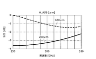
- FIG. 4 shows the passage characteristics of electromagnetic waves between the ports of FIG.
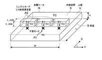
- FIG. 5 is an explanatory diagram showing a structural example of a module loaded with a plurality of single mode 1 ⁇ 4 wavelength waveguides.
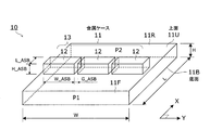
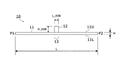
- FIG. 6 is a perspective view of the high frequency module according to the first embodiment.
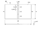
- FIG. 7 is a top view of the high frequency module according to the first embodiment.
- FIG. 8 is a side view of the high frequency module according to the first embodiment.
- FIG. 1 is an explanatory diagram showing a calculation model of the unnecessary mode.
- FIG. 2 is a graph showing the propagation characteristics of the unnecessary mode of FIG.
- FIG. 3 is an explanatory diagram showing a structural example of a high-frequency
- FIG. 9 is a graph showing pass characteristics of the high frequency module according to the first embodiment.
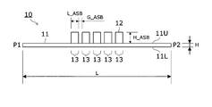
- FIG. 10 is a top view of the high frequency module according to the second embodiment.
- FIG. 11 is a side view of the high frequency module according to the second embodiment.
- FIG. 12 is a graph showing pass characteristics of the high frequency module according to the second embodiment.
- FIG. 13 is a side view of the high frequency module according to the third embodiment.
- FIG. 14 is a graph showing pass characteristics of the high frequency module according to the third embodiment.
- FIG. 1 is an explanatory diagram showing a calculation model of the unnecessary mode.
- a high-frequency module (not shown) is mounted on the bottom surface B of the metal case M, and the outside of the metal case M is entirely surrounded by a conductor.
- the wall surface of the metal case M is not a perfect conductor, and therefore the calculation model has severe conditions in which the leakage mode is more likely to propagate than in practical use. Therefore, it is practically sufficient if the leakage mode can be cut off by this calculation model.
- FIG. 2 is a graph showing the propagation characteristics of the unnecessary mode of FIG.
- the propagation characteristics of the modes propagating from the port P1 located on a pair of opposing side surfaces in the internal space S of FIG. 1 to the port P2 are almost the same for all modes TE10, TE20, and TE30. Pass without loss. It is considered that not only these three modes actually propagate but also more modes determined by the wavelength of the electromagnetic wave and the internal structure of the metal case M propagate.
- FIG. 3 is an explanatory diagram showing a structural example of a high-frequency module loaded with a 1/4 wavelength waveguide.
- a quarter wavelength waveguide A made of a stub waveguide is loaded on the upper surface U of the metal case M.
- This structure is a choke structure to which a method used for blocking the leakage of electromagnetic waves at the connection between waveguide flanges is applied.
- the electromagnetic wave WS propagating to the 1 ⁇ 4 wavelength waveguide A side, reflected and returned has a phase difference of 180 degrees from the electromagnetic wave WP propagating from the port P1 to the port P2. Therefore, it is considered that the electromagnetic wave WS and the electromagnetic wave WP cancel each other out in the portion marked with X in FIG. 3, and as a result, the effect of blocking the electromagnetic wave WP propagating from the port P1 to the port P2 is obtained.
- FIG. 4 shows the passage characteristics of electromagnetic waves between the ports of FIG.
- FIG. 4 shows the passage characteristic of the electromagnetic wave from the port P1 to the port P2 (the input to the port P1 is TE10 mode only).
- the blocking effect (amount of decrease in S21)
- the blocking effect it can be seen that when compared with FIG. 2, only about 4 dB is obtained at the maximum.
- signals cancel each other out at a frequency where the phase difference of electromagnetic waves becomes 180 degrees, so ideally the leakage should be completely blocked. You can see that it is small.
- the propagation constants of the respective modes generally have different values, so that the quarter-wave waveguide A is set to have a length of quarter wavelength with respect to the TE10 mode, for example. However, it does not become a quarter wavelength for other modes. For such a mode, the effect of canceling electromagnetic waves in the portion marked with X in FIG. 3 cannot be expected. Therefore, the structure of FIG. 3 cannot obtain a large blocking effect.
- the quarter wavelength waveguide A of FIG. 3 is divided into small quarter wavelength waveguides AS, and each of these quarter wavelength waveguides AS has only a single mode (TE10 mode).
- TE10 mode a single mode
- FIG. 5 is an explanatory diagram showing a structural example of a module loaded with a plurality of single mode 1 ⁇ 4 wavelength waveguides.
- a waveguide can limit the number of modes it propagates by limiting its size.
- a single mode is achieved by limiting the width and length of the quarter wavelength waveguide AS.
- the width and length of each quarter wavelength waveguide AS are set to be a quarter wavelength in the TE10 mode.
- each 1/4 wavelength waveguide AS has a dimension corresponding to 1/4 wavelength of the cutoff frequency indicating the frequency band of the target electromagnetic wave to be shielded, and each 1/4 wavelength
- the width and the length of the waveguide AS have such dimensions that only TE10 mode high frequencies can be propagated in the frequency band of the target electromagnetic wave.
- FIG. 6 is a perspective view of the high frequency module according to the first embodiment.
- FIG. 7 is a top view of the high frequency module according to the first embodiment.
- FIG. 8 is a side view of the high frequency module according to the first embodiment.
- the high frequency module 10 is a module that houses a high frequency circuit inside a metal case. In this embodiment, a specific example of the structure described in the principle of the invention will be described.
- the high frequency module 10 is formed of a hollow rectangular box body, and has a metal case 11 for housing the high frequency circuit in the inner space, and a high frequency circuit of the metal case 11.
- the height H_ABS of each of the waveguide structures 12 has a dimension corresponding to 1 ⁇ 4 wavelength of the cutoff frequency fo indicating the frequency band of the target electromagnetic wave to be shielded. Further, the width W_ABS and the length L_ABS of each of the waveguide structures 12 have dimensions such that only high-frequency TE10 mode can be propagated in the frequency band of the target electromagnetic wave. Further, these waveguide structures 12 are arranged in the second direction Y orthogonal to the first direction X in which the pair of ports P1 and P2 located on the pair of side surfaces 11F and 11R of the side surfaces of the metal case 11 face each other. Along the line, they are arranged in a row at intervals smaller than a quarter wavelength of the cutoff frequency fo.
- a structure in which a plurality of waveguide structures 12 are arranged in a line along the second direction Y is referred to as a blocking structure 13.
- 6 to 8 show an example in which the blocking structure 13 is composed of three waveguide structures 12, but the number of the waveguide structures 12 is not limited to three, and the number of arrangements is not limited to three. Should be 2 or more. The actual number of arrangements is determined based on the width W of the high frequency module 10 along the second direction Y and the size and spacing of the waveguide structure 12.
- G_ABS has a value smaller than a quarter wavelength of the cutoff frequency fo so as not to cause resonance at intervals between the waveguide structures 12. Therefore, for G_ABS, the minimum size (generally about 50 to 100 ⁇ m) of processing accuracy when processing the metal case 11 may be selected.
- G_ABS 50 um.
- FIG. 9 is a graph showing the pass characteristics of the high-frequency module according to the first embodiment, showing the pass characteristics of electromagnetic waves propagating from the port P1 to the port P2. It can be seen that when the height H_ABS of the waveguide structure 12 is 600 ⁇ m, a very large blocking effect of a blocking amount of 35 dB at 302 GHz is obtained. It can also be seen that by adjusting the length L_ABS of the waveguide structure 12, the frequency band in which a large blocking effect is obtained can be changed. Compared with the case of using the general choke structure of FIG. 4 described above, a very large amount of attenuation is obtained, so the effectiveness of this embodiment can be confirmed.
- the present invention does not require an electromagnetic wave absorber, and the waveguide structure 12 can be loaded only by processing the wall surface of the metal case 11 to change the shape. Therefore, it is possible to suppress an increase in work load and work cost in manufacturing the high frequency module.
- FIG. 10 is a top view of the high frequency module according to the second embodiment.
- FIG. 11 is a side view of the high frequency module according to the second embodiment.
- the blocking structure 13 described in the first embodiment is arranged in multiple stages in the first direction X.
- the waveguide structure 12 makes it possible to superimpose electromagnetic waves with a phase difference of 180 degrees, so ideally an infinite amount of attenuation can be obtained.
- G_ABS gap of finite length
- a part of the electromagnetic wave propagating from the port P1 to the port P2 is not coupled to the 1/4 wavelength and becomes a leakage signal as it is. I will end up. Therefore, infinite attenuation cannot be obtained.
- the frequency that becomes a quarter wavelength is only one frequency, so that a large amount of attenuation cannot be obtained at frequencies deviating from that frequency, and the structures of FIGS. 6 to 8 are as shown in FIG. Only a narrow band attenuation characteristic was obtained.
- the present embodiment proposes a structure in which the blocking structure 13 shown in FIGS. 6 to 8 is arranged in multiple stages in the electromagnetic wave propagation direction, that is, the first direction X to obtain a larger attenuation amount and a larger attenuation band.
- the multistage structure of the blocking structure 13 Due to the multistage structure of the blocking structure 13, a characteristic obtained by multiplying the attenuation characteristic of FIG. 9 by multiple stages is obtained, and the attenuation amount is increased. Further, in the vicinity of the attenuation peak in FIG. 9, the attenuation amount becomes large due to the characteristics being multiplied by the multi-stages, and as a result, the band in which the large attenuation amount is obtained becomes wider.
- the high-frequency module 10 is formed of a hollow rectangular box body, and includes a metal case 11 for housing a high-frequency circuit in an inner space, and a side surface of the metal case 11.
- a pair of high-frequency input/output ports P1 and P2 provided on each of the side surfaces 11F and 11R facing each other along the first direction X, and a bottom surface 11B of the metal case 11 on which a high-frequency circuit is mounted.
- the height H_ABS of each of these waveguide structures 12 has a dimension corresponding to a quarter wavelength of the cutoff frequency fo indicating the frequency band of the target electromagnetic wave to be blocked. doing. Further, the width W_ABS and the length L_ABS of each of the waveguide structures 12 have dimensions such that only high-frequency TE10 mode can be propagated in the frequency band of the target electromagnetic wave. In addition, each waveguide structure 12 is loaded in an array along the first direction X and the second direction Y at intervals smaller than a quarter wavelength of the high frequency wave in the TE10 mode.
- the blocking structure 13 is composed of three waveguide structures 12, but the number of the waveguide structures 12 arranged along the second direction Y is limited to three. However, the number of arrangements may be two or more. The actual number of arrangements is determined based on the width W of the high frequency module 10 along the second direction Y and the size and spacing of the waveguide structure 12. Further, the number of steps of the blocking structure 13 along the first direction X is determined by the number of overlapping electromagnetic waves.
- each waveguide structure 12 is the same as that in FIGS. 6 to 8.
- FIG. 12 is a graph showing pass characteristics of the high frequency module according to the second embodiment, showing pass characteristics of electromagnetic waves propagating from the port P1 to the port P2. It can be seen that a very large attenuation amount of 65 dB or more is obtained at 300 GHz. Further, a large attenuation amount of 40 dB is obtained even at 285 GHz, and the attenuation amount increasing effect and the band increasing effect of this embodiment can be seen.
- the total length of this structure (5 steps in the propagation direction) is as small as 2350 um.
- the electromagnetic wave absorber can obtain an attenuation of 40 dB, it is necessary to use an object having an attenuation of 20 dB/mm or more. It is difficult to obtain such a large attenuation amount with a general electromagnetic wave absorber such as doped Si, so that it is understood that the electromagnetic wave shielding effect of the present invention is very large.
- FIG. 13 is a side view of the high frequency module according to the third embodiment. In this embodiment, a method of widening the stop band will be described.
- the blocking structures 13 are arranged and loaded on the upper surface 11U of the metal case 11 along the first direction X. It is a configuration.
- the center frequency of the same cutoff band is set to fk.
- the center frequency fk of the stop band is determined by the height H_ABS of each waveguide structure 12 forming the stop structure 13, as described above. That is, the height of the waveguide structure 12 has a height corresponding to a quarter wavelength of the individual cutoff frequency fo for each of the waveguide structures 12 arranged along the second direction Y. There is. Note that the width W_ABS and the length L_ABS of each of the waveguide structures 12 are set such that only the high frequency wave in the TE10 mode can be propagated in the frequency band of the target electromagnetic wave, as in the first and second embodiments. Have
- FIG. 14 is a graph showing the pass characteristics of the high-frequency module according to the third embodiment, showing the pass characteristics of electromagnetic waves propagating from the port P1 to the port P2.
- the cut-off band having the center frequencies f1, f2,..., FN is formed for the electromagnetic wave propagating from the port P1 to the port P2. Therefore, as a whole, the configuration of FIG. 13 shows a wideband cutoff characteristic STx in which cutoff characteristics of the center frequencies f1, f2,..., FN are superimposed.
- the present embodiment can obtain a wider band cutoff characteristic than the first and second embodiments, it is applied to a high frequency module for mounting a wide band amplifier such as a distributed amplifier, and the bandwidth of the amplifier. It becomes possible to cut off leaked electromagnetic waves due to external oscillation, and it is possible to realize a very versatile electromagnetic wave blocking structure.
Landscapes
- Engineering & Computer Science (AREA)
- Power Engineering (AREA)
- Microelectronics & Electronic Packaging (AREA)
- Shielding Devices Or Components To Electric Or Magnetic Fields (AREA)
- Control Of Motors That Do Not Use Commutators (AREA)
- Microwave Amplifiers (AREA)
Abstract
金属ケース11のうち高周波回路が実装される底面11Bと対向する上面11Uに装荷された複数の導波管構造12を備え、これら導波管構造12のそれぞれの高さは、遮断対象とする対象電磁波の周波数帯域を示すカットオフ周波数foの1/4波長に相当する寸法を有し、これら導波管構造12の幅および長さは、対象電磁波の周波数帯域でTE10モードの高周波のみを伝搬可能とする寸法を有している。これにより、電波吸収体を用いることなく、金属ケース内部を伝搬する不要な電磁波を遮断する。
Description
本発明は、金属ケースの内側に高周波回路を収納する高周波モジュールの構成に関する高周波モジュール構成技術に関する。
光通信用電子回路やミリ波帯無線通信用電子回路などの高周波回路を収納する高周波モジュールは、通常、中空の矩形箱体からなる金属ケースが用いられる。このとき、金属ケース内部での電磁波の不要な伝搬がしばしば問題を引き起こす。不要な電磁波の伝搬は、回路からの放射に起因する場合が多い。すなわち、高周波回路を伝搬する電磁波が、高周波回路から放射され、空間を伝搬するモードへと結合するのである。これは、高周波帯では波長が短いため、高周波信号の入出力パッド部や幅の広い伝送線路などの回路部において、そのサイズが高周波信号の波長と同程度となるため、これら伝送媒体が放射体としての機能してしまうからである。また、回路およびモジュールのインピーダンス不連続部分における放射も存在する。金属ケースのインターフェースである同軸線路あるいは導波管と高周波回路との接続部分における接続損失の一部が空間へと放射するが、これはインピーダンス不整合により発生する放射の典型例である。
金属ケース内において回路から放射された電磁波は、高周波回路表面の金属パターンと金属ケース上面(高周波回路表面と対向する面)との間を伝搬する。この伝搬モードに対して金属ケースの側面は反射壁として作用するため、金属ケース内には共振器が形成される。このため、金属ケースの物理的なサイズで決定される共振が生じ、高周波モジュールの周波数特性に不要なリップルが発生する等の不具合を生じる。特に、高周波モジュールに実装される回路部品がアンプなどの増幅素子の場合、アンプの増幅機能により不要なリップルが強調されることがある。また、アンプの入出力端子が放射された電磁波によって結合し、アンプが発振することもある。
従来、金属ケース内を伝搬する不要な電磁波の伝搬を遮断するために、電波吸収体を用いる技術が提案されている(例えば、非特許文献1など参照)。この際、電波吸収体としては、例えば、ドープされた低抵抗シリコン基板などが用いられている。電波吸収体を金属ケースの上面や側面に配置することで、伝搬する不要モードが吸収され、上記のような不具合の発生が抑制されることになる。
Toshihiko KOSUGI et al., "120-GHz Tx/Rx Waveguide Modules for 10-Gbit/s Wireless Link System", Compound Semiconductor Integrated Circuit Symposium, 2006. CSIC 2006. IEEE, IEEE, December 2006
しかしながら、このような従来技術では、金属ケース上面や側面への電波吸収体の配置が必要となる。このためには、金属ケース内部の構造に合わせた電波吸収体の加工や、狭隘な金属ケース内部への電波吸収体の実装といった工程が必要となる。結果として、高周波モジュールの製造における、作業負担や作業コストが増大するという問題点があった。
本発明はこのような課題を解決するためのものであり、電波吸収体を用いることなく、金属ケース内部を伝搬する不要な電磁波を遮断できる高周波モジュール構成技術を提供することを目的としている。
このような目的を達成するために、本発明にかかる高周波モジュールは、中空の矩形箱体からなり、内側空間に高周波回路を収納する金属ケースと、前記金属ケースのうち前記高周波回路が実装される底面と対向する上面に装荷された複数の導波管構造を備え、前記複数の導波管構造のそれぞれの高さは、遮断対象とする対象電磁波の周波数帯域を示すカットオフ周波数の1/4波長に相当する寸法を有し、前記複数の導波管構造のそれぞれの幅および長さは、前記周波数帯域でTE10モードの高周波のみを伝搬可能とする寸法を有している。
また、本発明にかかる上記高周波モジュールの一構成例は、前記上面のうち前記対象電磁波が伝搬する第1の方向と直交する第2の方向に沿って、前記1/4波長より小さな間隔で一列に装荷されている。
また、本発明にかかる上記高周波モジュールの一構成例は、前記複数の導波管構造が、前記上面のうち前記対象電磁波が伝搬する第1の方向および前記第1の方向と直交する第2の方向に沿って、前記1/4波長より小さな間隔でアレイ状に装荷されている。
また、本発明にかかる上記高周波モジュールの一構成例は、前記複数の導波管構造が、前記第2の方向に沿って並ぶ導波管構造ごとに、それぞれ個別のカットオフ周波数の1/4波長に相当する高さを有している。
本発明によれば、ポート間を伝搬する電磁波が各導波管構造を伝搬する電磁波と打ち消しあうことになる。このため、電波吸収体を用いることなく、内部を伝搬する不要な電磁波を遮断することが可能となる。したがって、高周波モジュールの製造における、作業負担や作業コストの増大を抑制することが可能となる。
[発明の原理]
まず、本発明の原理を説明する。図1は、不要モードの計算モデルを示す説明図である。高周波モジュールの金属ケースM内での漏洩モードの伝搬を説明するために、図1に示すような、不要モード(主要伝送モード)の計算モデルとして金属ケースMの内部空間Sを考える。この内部空間Sには、金属ケースMの底面Bに高周波モジュール(図示せず)が実装され、金属ケースMの外側はすべて完全導体で囲われているものとする。なお、実際の高周波モジュールにおいては、金属ケースMの壁面は完全導体ではないため、本計算モデルでは、実用よりも漏洩モードが伝搬しやすい厳しい条件になっている。したがって、本計算モデルで漏洩モードが遮断できれば実用上十分である。
まず、本発明の原理を説明する。図1は、不要モードの計算モデルを示す説明図である。高周波モジュールの金属ケースM内での漏洩モードの伝搬を説明するために、図1に示すような、不要モード(主要伝送モード)の計算モデルとして金属ケースMの内部空間Sを考える。この内部空間Sには、金属ケースMの底面Bに高周波モジュール(図示せず)が実装され、金属ケースMの外側はすべて完全導体で囲われているものとする。なお、実際の高周波モジュールにおいては、金属ケースMの壁面は完全導体ではないため、本計算モデルでは、実用よりも漏洩モードが伝搬しやすい厳しい条件になっている。したがって、本計算モデルで漏洩モードが遮断できれば実用上十分である。
図2は、図1の不要モードの伝搬特性を示すグラフである。図1の内部空間Sのうち対向する一対の側面に位置するポートP1からポートP2へ伝搬するモードの伝搬特性は、図2に示すように、TE10,TE20,TE30のいずれのモードについても、ほとんど損失なく通過する。実際に伝搬するモードは、これら3つだけではなく、電磁波の波長と金属ケースMの内部構造で決定される、より多くのモードが伝搬すると考えられる。なお、内部空間Sの大きさは、幅W=2000um,長さL=4000um,高さH=150umとした。
図3は、1/4波長導波管を装荷した高周波モジュールの構造例を示す説明図である。図2に示した漏洩モードを遮断するような金属ケースMの内部構造を考える。図3の構造例は、金属ケースMの上面Uにスタブ導波管からなる1/4波長導波管Aを装荷したものである。この構造は、チョーク構造として、導波管フランジ同士の接続部における電磁波の漏洩を遮断する手法に用いられる手法を応用したものである。
図3のように、1/4波長導波管A側に伝搬し、反射して戻ってきた電磁波WSは、ポートP1からポートP2へと伝搬する電磁波WPとの位相差が180度になる。このため、図3の×印の部分では電磁波WSと電磁波WPとが打ち消しあい、結果として、ポートP1からポートP2へと伝搬する電磁波WPを遮断する効果が得られると考えられる。
図3のように、1/4波長導波管A側に伝搬し、反射して戻ってきた電磁波WSは、ポートP1からポートP2へと伝搬する電磁波WPとの位相差が180度になる。このため、図3の×印の部分では電磁波WSと電磁波WPとが打ち消しあい、結果として、ポートP1からポートP2へと伝搬する電磁波WPを遮断する効果が得られると考えられる。
しかしながら、チョークフランジ等で一般に用いられるこのような手法では、良好な遮断効果を得ることができない。図4は、図3のポート間における電磁波の通過特性である。図4には、ポートP1からポートP2への電磁波(ポートP1への入力はTE10モードのみとした)の通過特性が示されている。遮断効果(S21の減少量)としては、図2と比較すると、最大でも4dB程度しか得られていないことがわかる。通常の1/4波長線路による遮断では、電磁波の位相差が180度になる周波数で信号が打ち消しあうため、理想的には完全に漏洩が遮断されるはずであるから、図3の遮断効果が小さいことがわかる。
また、図4からは、遮断用の1/4波長導波管Aの長さH_ABSを200umまたは600umと大きく変化させても、通過特性には明瞭な遮断ピークは現れていないことがわかる。これらは、図3の1/4波長導波管Aがシングルモード導波管ではないことに起因する。
このことについてより詳細に説明する。ポートP1への入力がTE10モードのみであっても、1/4波長導波管Aと接続部とのインピーダンス不連続において、TE20,TE30,…等のマルチモードが励振される。ここで、各モードの伝搬定数は、一般には異なる値をとることに留意すれば、1/4波長導波管Aが、例えばTE10モードに対して1/4波長の長さに設定されていたとしても、他のモードに対しては1/4波長とならない。そのようなモードに対しては、図3の×印の部分における電磁波の打ち消し効果を期待できない。したがって、図3の構造では、大きな遮断効果を得ることができないのである。
このことについてより詳細に説明する。ポートP1への入力がTE10モードのみであっても、1/4波長導波管Aと接続部とのインピーダンス不連続において、TE20,TE30,…等のマルチモードが励振される。ここで、各モードの伝搬定数は、一般には異なる値をとることに留意すれば、1/4波長導波管Aが、例えばTE10モードに対して1/4波長の長さに設定されていたとしても、他のモードに対しては1/4波長とならない。そのようなモードに対しては、図3の×印の部分における電磁波の打ち消し効果を期待できない。したがって、図3の構造では、大きな遮断効果を得ることができないのである。
そこで、本発明では、図3の1/4波長導波管Aを小さい1/4波長導波管ASに分割し、これら1/4波長導波管ASのそれぞれはシングルモード(TE10モード)しか伝搬できないような構成とする構造を提案する。図5は、複数のシングルモード1/4波長導波管を装荷したモジュールの構造例を示す説明図である。
一般に、導波管は、そのサイズを制限することによって、伝搬するモード数を制限することができる。図5の例では、1/4波長導波管ASの幅および長さを制限することによって、シングルモード化を図っている。各1/4波長導波管ASの幅および長さは、TE10モードにおいて1/4波長となるように設定されている。
一般に、導波管は、そのサイズを制限することによって、伝搬するモード数を制限することができる。図5の例では、1/4波長導波管ASの幅および長さを制限することによって、シングルモード化を図っている。各1/4波長導波管ASの幅および長さは、TE10モードにおいて1/4波長となるように設定されている。
すなわち、各1/4波長導波管ASの高さは、遮断対象となる対象電磁波の周波数帯域を示すカットオフ周波数の1/4波長に相当する寸法を有しており、各1/4波長導波管ASの幅および長さは、対象電磁波の周波数帯域でTE10モードの高周波のみを伝搬可能とする寸法を有している。
このような構造をとることによって、ポートP1からポートP2へと伝搬する電磁波は、各1/4波長導波管ASを伝搬する電磁波と、図5の×印部分で完全に打ち消しあうことになり、大きな遮断効果を得ることができる。
このような構造をとることによって、ポートP1からポートP2へと伝搬する電磁波は、各1/4波長導波管ASを伝搬する電磁波と、図5の×印部分で完全に打ち消しあうことになり、大きな遮断効果を得ることができる。
次に、本発明の実施の形態について図面を参照して説明する。
[第1の実施の形態]
まず、図6~図8を参照して、本発明の第1の実施の形態にかかる高周波モジュール10について説明する。図6は、第1の実施の形態にかかる高周波モジュールの斜視図である。図7は、第1の実施の形態にかかる高周波モジュールの上面図である。図8は、第1の実施の形態にかかる高周波モジュールの側面図である。
この高周波モジュール10は、金属ケースの内側に高周波回路を収納するモジュールである。本実施の形態では、発明の原理で説明した構造の具体例について説明する。
[第1の実施の形態]
まず、図6~図8を参照して、本発明の第1の実施の形態にかかる高周波モジュール10について説明する。図6は、第1の実施の形態にかかる高周波モジュールの斜視図である。図7は、第1の実施の形態にかかる高周波モジュールの上面図である。図8は、第1の実施の形態にかかる高周波モジュールの側面図である。
この高周波モジュール10は、金属ケースの内側に高周波回路を収納するモジュールである。本実施の形態では、発明の原理で説明した構造の具体例について説明する。
図6~図8に示すように、本実施の形態にかかる高周波モジュール10は、中空の矩形箱体からなり、内側空間に高周波回路を収納する金属ケース11と、金属ケース11のうち高周波回路が実装される底面11B(高周波回路の金属パターンが形成された高周波回路表面)と対向する上面11Uに装荷された、図5の1/4波長導波管ASからなる複数の導波管構造12とを備えている。
本実施の形態において、これら導波管構造12のそれぞれの高さH_ABSは、遮断対象とする対象電磁波の周波数帯域を示すカットオフ周波数foの1/4波長に相当する寸法を有している。また、これら導波管構造12のそれぞれの幅W_ABSおよび長さL_ABSは、対象電磁波の周波数帯域でTE10モードの高周波のみを伝搬可能とする寸法を有している。
また、これら導波管構造12は、金属ケース11の側面のうち、一対の側面11F,11Rに位置する一対のポートP1,P2が対向する第1の方向Xと直交する第2の方向Yに沿って、カットオフ周波数foの1/4波長より小さな間隔で一列に配置されている。
また、これら導波管構造12は、金属ケース11の側面のうち、一対の側面11F,11Rに位置する一対のポートP1,P2が対向する第1の方向Xと直交する第2の方向Yに沿って、カットオフ周波数foの1/4波長より小さな間隔で一列に配置されている。
以下では、複数の導波管構造12が第2の方向Yに沿って一列に配置された構造を遮断構造13という。図6~図8には、遮断構造13が3つの導波管構造12からなる例が示されているが、導波管構造12の配置数は3つに限定されるものではなく、配置数は2以上であればよい。実際の配置数は、高周波モジュール10の第2の方向Yに沿った幅Wと導波管構造12のサイズや間隔に基づいて決定される。
導波管構造12の高さH_ABSは、前述のように、カットオフ周波数foの1/4波長になるように設定される。これにより、導波管構造12はシングルモード1/4波長導波管となる。また、導波管構造12の第2の方向Yに沿った幅W_ABSと、第1の方向Xに沿った長さL_ABSは、カットオフ周波数foを決定するパラメータとなる。例えば、300GHz帯の漏洩電磁波を遮断したい場合には、300GHz帯で、導波管構造12がTE10モードのみを伝搬するようにW_ABSおよびL_ABSを定めればよい。ここでは、このようなパラメータの一例として、W_ABS=630um,L_ABS=430umを選択した。カットオフ周波数foの1/4波長とW_ABSおよびL_ABSとの関係については、一般的な公知の計算手法に基づき特定すればよい。
導波管構造12同士の第2の方向Yに沿った間隔G_ABSについては、小さければ小さいほど、ポートP1からポートP2へと伝搬する対象電磁波を取りこぼしなく導波管構造12へと結合させることができるため、大きな遮断効果を得ることができる。この際、導波管構造12間の間隔での共振を生じさせないように、G_ABSはカットオフ周波数foの1/4波長よりも小さい値であることが望ましい。そのため、G_ABSは、金属ケース11を加工する際の、加工精度の最小寸法(一般には50-100um程度)を選択すればよい。ここでは、G_ABS=50umとした。
図9は、第1の実施の形態にかかる高周波モジュールの通過特性を示すグラフであり、ポートP1からポートP2へと伝搬する電磁波の通過特性が示されている。導波管構造12の高さH_ABS=600umのときに、302GHzにおいて遮断量35dBという、非常に大きな遮断効果が得られていることがわかる。また、導波管構造12の長さL_ABSを調節することによって、大きな遮断効果の得られる周波数帯を変更することができることもわかる。前述した図4の一般的なチョーク構造を用いる場合と比較して、非常に大きな減衰量が得られていることから、本実施の形態の有効性が確認できる。
また、発明の原理で述べたように、本発明では電波吸収体を必要とせず、金属ケース11の壁面を加工して形状を変更するだけで、導波管構造12を装荷することができる。したがって、高周波モジュールの製造における、作業負担や作業コストの増大を抑制することが可能となる。
[第2の実施の形態]
次に、図10および図11を参照して、本発明の第2の実施の形態にかかる高周波モジュール10について説明する。図10は、第2の実施の形態にかかる高周波モジュールの上面図である。図11は、第2の実施の形態にかかる高周波モジュールの側面図である。
本実施の形態では、第1の実施の形態で述べた遮断構造13を、第1の方向Xに多段配置した構成について説明する。
次に、図10および図11を参照して、本発明の第2の実施の形態にかかる高周波モジュール10について説明する。図10は、第2の実施の形態にかかる高周波モジュールの上面図である。図11は、第2の実施の形態にかかる高周波モジュールの側面図である。
本実施の形態では、第1の実施の形態で述べた遮断構造13を、第1の方向Xに多段配置した構成について説明する。
導波管構造12を用いれば180度の位相差をもって電磁波を重ね合わせることができるため、理想的には無限大の減衰量を得ることが可能となる。しかし、第1の実施の形態で述べた通り、有限長の間隔G_ABSの隙間により、ポートP1からポートP2へ伝搬する電磁波の一部は1/4波長に結合せず、そのまま漏洩信号となってしまう。そのため、無限大の減衰量を得ることはできていない。また、1/4波長となる周波数は厳密には一周波数のみであるから、その周波数から外れた周波数では、あまり大きな減衰量は得られず、図6-図8の構造では図9に示すように狭帯域な減衰特性しか得られなかった。
そこで、本実施の形態では、図6-図8の遮断構造13を、電磁波伝搬方向すなわち第1の方向Xに対して多段配置することで、より大きな減衰量と大きな減衰帯域を得る構造を提案する。
このような遮断構造13の多段化によって、図9の減衰特性を多段回数掛け合わせたような特性が得られ、減衰量が大きくなる。また、図9の減衰ピーク周辺の、中程度の減衰量の箇所も、多段化で特性が掛け合わされることによって、その減衰量は大きくなり、結果として大きな減衰量が得られる帯域も広くなる。
このような遮断構造13の多段化によって、図9の減衰特性を多段回数掛け合わせたような特性が得られ、減衰量が大きくなる。また、図9の減衰ピーク周辺の、中程度の減衰量の箇所も、多段化で特性が掛け合わされることによって、その減衰量は大きくなり、結果として大きな減衰量が得られる帯域も広くなる。
図10および図11に示すように、本実施の形態にかかる高周波モジュール10は、中空の矩形箱体からなり、内側空間に高周波回路を収納する金属ケース11と、金属ケース11の側面のうち、第1の方向Xに沿って対向する側面11F,11Rのそれぞれに設けられた、高周波入出力用の1対のポートP1,P2と、金属ケース11のうち高周波回路が実装される底面11Bと対向する上面11Uに装荷された、スタブ導波管からなる複数の導波管構造12とを備えている。
第1の実施の形態と同様に、これら導波管構造12のそれぞれの高さH_ABSは、遮断対象とする対象電磁波の周波数帯域を示すカットオフ周波数foの1/4波長に相当する寸法を有している。また、これら導波管構造12のそれぞれの幅W_ABSおよび長さL_ABSは、対象電磁波の周波数帯域でTE10モードの高周波のみを伝搬可能とする寸法を有している。これに加えて、各導波管構造12は、第1の方向Xおよび第2の方向Yに沿って、TE10モードの高周波の1/4波長より小さな間隔でアレイ状に装荷されている。
図10および図11には、遮断構造13が3つの導波管構造12からなる例が示されているが、第2の方向Yに沿った導波管構造12の配置数は3つに限定されるものではなく、配置数は2以上であればよい。実際の配置数は、高周波モジュール10の第2の方向Yに沿った幅Wと導波管構造12のサイズや間隔に基づいて決定される。また、第1の方向Xに沿った遮断構造13の段数は、重ね合わせる電磁波の数で決定される。
図10および図11では、各々の導波管構造12のサイズは図6-図8と同じものを採用した。各導波管構造12の高さH_ABSについては、300GHz付近で大きな減衰量の得られる600umを共通で選択した。また、多段化する際の導波管同士の間隔G-ABSは、第1の実施の形態と同じ理由で、できるだけ小さい方が良い。そこで、第1の実施の形態同様に、金属ケース加工の最小寸法(一般には50-100um程度)を選択すればよい。ここでは、G_ABS=50umとした。また、段数は5段とした。
図12は、第2の実施の形態にかかる高周波モジュールの通過特性を示すグラフであり、ポートP1からポートP2へと伝搬する電磁波の通過特性が示されている。300GHzにおいて65dB以上もの非常に大きな減衰量が得られていることがわかる。また、285GHzにおいても40dBという大きな減衰量が得られており、本実施の形態の、減衰量増大効果、帯域増大効果が見て取れる。
このように非常に大きな減衰量が得られるにもかかわらず、本構造のトータル長(伝搬方向の5段分の長さ)は2350umと小型である。仮に、40dBの減衰量を電波吸収体で得ようと考えると、20dB/mm以上の減衰量を持つような物体を用いる必要がある。ドープトSiなどの一般の電波吸収体ではここまでの大きな減衰量を得ることは難しいため、本発明の電磁波遮断効果が非常に大きいことがわかる。
[第3の実施の形態]
次に、図13を参照して、本発明の第3の実施の形態にかかる高周波モジュール10について説明する。図13は、第3の実施の形態にかかる高周波モジュールの側面図である。
本実施の形態では、遮断帯域を広帯域化する手法について述べる。
次に、図13を参照して、本発明の第3の実施の形態にかかる高周波モジュール10について説明する。図13は、第3の実施の形態にかかる高周波モジュールの側面図である。
本実施の形態では、遮断帯域を広帯域化する手法について述べる。
図13に示すように、本実施の形態にかかる高周波モジュール10は、第2の実施の形態と同様に、金属ケース11の上面11Uに、第1の方向Xに沿って遮断構造13を並べて装荷した構成である。図13において、遮断構造体STk(k=1,2,…,n)は、第1または第2の実施の形態に係る遮断構造13が1つまたは複数段まとまったものであり、同一遮断構造体STkに属する遮断構造13については、同一の遮断帯域の中心周波数がfkに設定されている。
遮断帯域の中心周波数fkは、前述したように、遮断構造13を構成する各導波管構造12の高さH_ABSで決定される。すなわち、導波管構造12の高さが、第2の方向Yに沿って並ぶ導波管構造12ごとに、それぞれ個別のカットオフ周波数foの1/4波長に相当する高さを有している。なお、これら導波管構造12のそれぞれの幅W_ABSおよび長さL_ABSは、第1および第2の実施の形態と同様に、対象電磁波の周波数帯域でTE10モードの高周波のみを伝搬可能とする寸法を有している。
図14は、第3の実施の形態にかかる高周波モジュールの通過特性を示すグラフであり、ポートP1からポートP2へと伝搬する電磁波の通過特性が示されている。このような構成をとることにより、ポートP1からポートP2に伝搬する電磁波に対して、中心周波数f1,f2,…,fNの遮断帯域が形成される。したがって、図13の構成は、全体として、図14に示すように、中心周波数f1,f2,…,fNの遮断特性が重ね合わされたような広帯域の遮断特性STxを示す。
本実施の形態によって、第1および第2の実施の形態よりも広帯域な遮断特性が得られるため、例えば、分布増幅器のような広帯域増幅器を実装するための高周波モジュールへの応用や、増幅器の帯域外発振による漏洩電磁波の遮断を行うことができるようになり、非常に汎用性の高い電磁波遮断構造が実現できる。
[実施の形態の拡張]
以上、実施形態を参照して本発明を説明したが、本発明は上記実施形態に限定されるものではない。本発明の構成や詳細には、本発明のスコープ内で当業者が理解しうる様々な変更をすることができる。また、各実施形態については、矛盾しない範囲で任意に組み合わせて実施することができる。
以上、実施形態を参照して本発明を説明したが、本発明は上記実施形態に限定されるものではない。本発明の構成や詳細には、本発明のスコープ内で当業者が理解しうる様々な変更をすることができる。また、各実施形態については、矛盾しない範囲で任意に組み合わせて実施することができる。
10…高周波モジュール、11…金属ケース、11F,11R…側面、11B…底面、11U…上面、12…導波管構造、13…遮断構造、STk…遮断構造体、P1,P2…ポート。
Claims (4)
- 中空の矩形箱体からなり、内側空間に高周波回路を収納する金属ケースと、
前記金属ケースのうち前記高周波回路が実装される底面と対向する上面に装荷された複数の導波管構造を備え、
前記複数の導波管構造のそれぞれの高さは、遮断対象とする対象電磁波の周波数帯域を示すカットオフ周波数の1/4波長に相当する寸法を有し、
前記複数の導波管構造のそれぞれの幅および長さは、前記周波数帯域でTE10モードの高周波のみを伝搬可能とする寸法を有する
ことを特徴とする高周波モジュール。 - 請求項1に記載の高周波モジュールにおいて、
前記複数の導波管構造は、前記上面のうち前記対象電磁波が伝搬する第1の方向と直交する第2の方向に沿って、前記1/4波長より小さな間隔で一列に装荷されていることを特徴とする高周波モジュール。 - 請求項1に記載の高周波モジュールにおいて、
前記複数の導波管構造は、前記上面のうち前記対象電磁波が伝搬する第1の方向および前記第1の方向と直交する第2の方向に沿って、前記1/4波長より小さな間隔でアレイ状に装荷されていることを特徴とする高周波モジュール。 - 請求項3に記載の高周波モジュールにおいて、
前記複数の導波管構造は、前記第2の方向に沿って並ぶ導波管構造ごとに、それぞれ個別のカットオフ周波数の1/4波長に相当する高さを有していることを特徴とする高周波モジュール。
Priority Applications (1)
| Application Number | Priority Date | Filing Date | Title |
|---|---|---|---|
| US17/312,046 US11749873B2 (en) | 2018-12-11 | 2019-11-27 | High-frequency module |
Applications Claiming Priority (2)
| Application Number | Priority Date | Filing Date | Title |
|---|---|---|---|
| JP2018231609A JP7095582B2 (ja) | 2018-12-11 | 2018-12-11 | 高周波モジュール |
| JP2018-231609 | 2018-12-11 |
Publications (1)
| Publication Number | Publication Date |
|---|---|
| WO2020121815A1 true WO2020121815A1 (ja) | 2020-06-18 |
Family
ID=71076945
Family Applications (1)
| Application Number | Title | Priority Date | Filing Date |
|---|---|---|---|
| PCT/JP2019/046371 Ceased WO2020121815A1 (ja) | 2018-12-11 | 2019-11-27 | 高周波モジュール |
Country Status (3)
| Country | Link |
|---|---|
| US (1) | US11749873B2 (ja) |
| JP (1) | JP7095582B2 (ja) |
| WO (1) | WO2020121815A1 (ja) |
Families Citing this family (1)
| Publication number | Priority date | Publication date | Assignee | Title |
|---|---|---|---|---|
| KR20220121104A (ko) * | 2021-02-24 | 2022-08-31 | 삼성전자주식회사 | 멀티 모드 공진기 및 이를 포함하는 양자 컴퓨팅 소자 |
Citations (3)
| Publication number | Priority date | Publication date | Assignee | Title |
|---|---|---|---|---|
| JP2003258504A (ja) * | 2002-02-26 | 2003-09-12 | Murata Mfg Co Ltd | 高周波回路装置および送受信装置 |
| JP2010252182A (ja) * | 2009-04-17 | 2010-11-04 | Furuno Electric Co Ltd | 高調波遮断フィルタ及びレーダ装置 |
| US20140132153A1 (en) * | 2012-11-12 | 2014-05-15 | Lg Electronics Inc. | Lighting apparatus |
Family Cites Families (6)
| Publication number | Priority date | Publication date | Assignee | Title |
|---|---|---|---|---|
| US3058072A (en) * | 1956-11-15 | 1962-10-09 | Raytheon Co | Microwave filters |
| DE1566027A1 (de) * | 1967-10-06 | 1970-07-23 | Rafena Werke Radeberg Veb | Tiefpassfilter fuer Hohlleiterwellen |
| JPH02190001A (ja) * | 1989-01-18 | 1990-07-26 | Nec Corp | コルゲート型ろ波器 |
| JP3739230B2 (ja) | 1999-04-26 | 2006-01-25 | 株式会社日立製作所 | 高周波通信装置 |
| WO2001067837A1 (fr) | 2000-03-06 | 2001-09-13 | Fujitsu Limited | Plaque metallique blindee et dispositif a circuit utilisant cette plaque metallique blindee |
| JP2003008313A (ja) | 2001-06-20 | 2003-01-10 | Hitachi Kokusai Electric Inc | マイクロストリップ導波管変換回路 |
-
2018
- 2018-12-11 JP JP2018231609A patent/JP7095582B2/ja active Active
-
2019
- 2019-11-27 US US17/312,046 patent/US11749873B2/en active Active
- 2019-11-27 WO PCT/JP2019/046371 patent/WO2020121815A1/ja not_active Ceased
Patent Citations (3)
| Publication number | Priority date | Publication date | Assignee | Title |
|---|---|---|---|---|
| JP2003258504A (ja) * | 2002-02-26 | 2003-09-12 | Murata Mfg Co Ltd | 高周波回路装置および送受信装置 |
| JP2010252182A (ja) * | 2009-04-17 | 2010-11-04 | Furuno Electric Co Ltd | 高調波遮断フィルタ及びレーダ装置 |
| US20140132153A1 (en) * | 2012-11-12 | 2014-05-15 | Lg Electronics Inc. | Lighting apparatus |
Also Published As
| Publication number | Publication date |
|---|---|
| JP2020096030A (ja) | 2020-06-18 |
| JP7095582B2 (ja) | 2022-07-05 |
| US20220029259A1 (en) | 2022-01-27 |
| US11749873B2 (en) | 2023-09-05 |
Similar Documents
| Publication | Publication Date | Title |
|---|---|---|
| JP4016900B2 (ja) | 導波管装置 | |
| US8072288B2 (en) | Directional coupler | |
| JP4257225B2 (ja) | マイクロストリップと導波路の間のトランジッション及びこのトランジッションを組み込んだ外部送受信ユニット | |
| JP5755546B2 (ja) | 電力合成分配器、電力増幅回路および無線装置 | |
| US6741142B1 (en) | High-frequency circuit element having means for interrupting higher order modes | |
| US11394095B2 (en) | Dielectric filter, array antenna device | |
| CN117136473A (zh) | 复合谐振器以及集合体 | |
| CN113381701A (zh) | 微波固态功率放大器 | |
| US11749873B2 (en) | High-frequency module | |
| US4648128A (en) | Microwave integrated circuit immune to adverse shielding effects | |
| KR100852377B1 (ko) | 소형 nrd 가이드벤드 | |
| JP2009296306A (ja) | 配線基板 | |
| JP4262192B2 (ja) | 非導波管線路−導波管変換器 | |
| JP2003008309A (ja) | マイクロ波帯干渉防止パッケージ | |
| US7408430B2 (en) | High-frequency circuit device and transmitting and receiving apparatus | |
| JP5981466B2 (ja) | 平面伝送線路導波管変換器 | |
| JP2006191428A (ja) | マイクロストリップ線路導波管変換器 | |
| KR102549082B1 (ko) | 고차모드를 억제하는 광대역 셉텀 편파기 | |
| WO2014132657A1 (ja) | 有極型帯域通過フィルタ | |
| US20220045412A1 (en) | Polarized waveguide filter and antenna feeding circuit | |
| US7978022B2 (en) | Cable to waveguide transition apparatus having signal accumulation form of backshort and active phase shifting using the same | |
| JP6144456B2 (ja) | 高周波モジュール | |
| Morimoto et al. | Suppression of cavity resonant coupling by L-shaped metal plate on microwave module lid | |
| JP4238177B2 (ja) | 受信帯域雑音抑圧フィルタ内蔵送信機 | |
| JP2010252182A (ja) | 高調波遮断フィルタ及びレーダ装置 |
Legal Events
| Date | Code | Title | Description |
|---|---|---|---|
| 121 | Ep: the epo has been informed by wipo that ep was designated in this application |
Ref document number: 19897198 Country of ref document: EP Kind code of ref document: A1 |
|
| NENP | Non-entry into the national phase |
Ref country code: DE |
|
| 122 | Ep: pct application non-entry in european phase |
Ref document number: 19897198 Country of ref document: EP Kind code of ref document: A1 |