WO2020121097A1 - Dispositif électroluminescent, appareil électroluminescent, dispositif électronique et dispositif d'éclairage - Google Patents
Dispositif électroluminescent, appareil électroluminescent, dispositif électronique et dispositif d'éclairage Download PDFInfo
- Publication number
- WO2020121097A1 WO2020121097A1 PCT/IB2019/060207 IB2019060207W WO2020121097A1 WO 2020121097 A1 WO2020121097 A1 WO 2020121097A1 IB 2019060207 W IB2019060207 W IB 2019060207W WO 2020121097 A1 WO2020121097 A1 WO 2020121097A1
- Authority
- WO
- WIPO (PCT)
- Prior art keywords
- light
- electrode
- emitting device
- light emitting
- abbreviation
- Prior art date
Links
- 239000010410 layer Substances 0.000 claims description 278
- 239000000463 material Substances 0.000 claims description 119
- 239000000126 substance Substances 0.000 claims description 81
- 125000001997 phenyl group Chemical group [H]C1=C([H])C([H])=C(*)C([H])=C1[H] 0.000 claims description 31
- 125000002524 organometallic group Chemical group 0.000 claims description 24
- 125000004432 carbon atom Chemical group C* 0.000 claims description 19
- 239000010949 copper Substances 0.000 claims description 18
- 239000010931 gold Substances 0.000 claims description 14
- 125000000217 alkyl group Chemical group 0.000 claims description 13
- 239000003446 ligand Substances 0.000 claims description 12
- RYGMFSIKBFXOCR-UHFFFAOYSA-N Copper Chemical compound [Cu] RYGMFSIKBFXOCR-UHFFFAOYSA-N 0.000 claims description 9
- BQCADISMDOOEFD-UHFFFAOYSA-N Silver Chemical compound [Ag] BQCADISMDOOEFD-UHFFFAOYSA-N 0.000 claims description 9
- 229910052802 copper Inorganic materials 0.000 claims description 9
- 229910052709 silver Inorganic materials 0.000 claims description 9
- 239000004332 silver Substances 0.000 claims description 9
- PCHJSUWPFVWCPO-UHFFFAOYSA-N gold Chemical compound [Au] PCHJSUWPFVWCPO-UHFFFAOYSA-N 0.000 claims description 7
- 229910052737 gold Inorganic materials 0.000 claims description 7
- 125000001624 naphthyl group Chemical group 0.000 claims description 6
- 239000012044 organic layer Substances 0.000 claims description 6
- 239000001257 hydrogen Substances 0.000 claims description 5
- 229910052739 hydrogen Inorganic materials 0.000 claims description 5
- UFHFLCQGNIYNRP-UHFFFAOYSA-N Hydrogen Chemical compound [H][H] UFHFLCQGNIYNRP-UHFFFAOYSA-N 0.000 claims description 4
- 239000000758 substrate Substances 0.000 description 91
- 230000006870 function Effects 0.000 description 47
- 150000002894 organic compounds Chemical class 0.000 description 46
- -1 (Yb) Chemical class 0.000 description 45
- 238000002347 injection Methods 0.000 description 43
- 239000007924 injection Substances 0.000 description 43
- 238000000034 method Methods 0.000 description 36
- 150000001875 compounds Chemical class 0.000 description 29
- MILUBEOXRNEUHS-UHFFFAOYSA-N iridium(3+) Chemical compound [Ir+3] MILUBEOXRNEUHS-UHFFFAOYSA-N 0.000 description 28
- 229910052741 iridium Inorganic materials 0.000 description 27
- GKOZUEZYRPOHIO-UHFFFAOYSA-N iridium atom Chemical compound [Ir] GKOZUEZYRPOHIO-UHFFFAOYSA-N 0.000 description 26
- 238000000295 emission spectrum Methods 0.000 description 24
- 239000007983 Tris buffer Substances 0.000 description 21
- CUJRVFIICFDLGR-UHFFFAOYSA-N acetylacetonate Chemical compound CC(=O)[CH-]C(C)=O CUJRVFIICFDLGR-UHFFFAOYSA-N 0.000 description 21
- 229910052757 nitrogen Inorganic materials 0.000 description 20
- 238000007740 vapor deposition Methods 0.000 description 19
- 238000010586 diagram Methods 0.000 description 18
- 230000032258 transport Effects 0.000 description 18
- 230000005525 hole transport Effects 0.000 description 16
- 239000004065 semiconductor Substances 0.000 description 16
- 230000005284 excitation Effects 0.000 description 14
- 125000005595 acetylacetonate group Chemical group 0.000 description 13
- 229910052799 carbon Inorganic materials 0.000 description 13
- 230000005281 excited state Effects 0.000 description 13
- 238000007789 sealing Methods 0.000 description 13
- OKKJLVBELUTLKV-UHFFFAOYSA-N Methanol Chemical compound OC OKKJLVBELUTLKV-UHFFFAOYSA-N 0.000 description 12
- 239000011159 matrix material Substances 0.000 description 12
- 239000000203 mixture Substances 0.000 description 12
- ODHXBMXNKOYIBV-UHFFFAOYSA-N triphenylamine Chemical compound C1=CC=CC=C1N(C=1C=CC=CC=1)C1=CC=CC=C1 ODHXBMXNKOYIBV-UHFFFAOYSA-N 0.000 description 12
- 229910052751 metal Inorganic materials 0.000 description 11
- YLQBMQCUIZJEEH-UHFFFAOYSA-N tetrahydrofuran Natural products C=1C=COC=1 YLQBMQCUIZJEEH-UHFFFAOYSA-N 0.000 description 11
- 238000004519 manufacturing process Methods 0.000 description 10
- 239000002184 metal Substances 0.000 description 10
- 230000003287 optical effect Effects 0.000 description 10
- 238000004088 simulation Methods 0.000 description 10
- UHOVQNZJYSORNB-UHFFFAOYSA-N Benzene Chemical compound C1=CC=CC=C1 UHOVQNZJYSORNB-UHFFFAOYSA-N 0.000 description 9
- YMWUJEATGCHHMB-UHFFFAOYSA-N Dichloromethane Chemical compound ClCCl YMWUJEATGCHHMB-UHFFFAOYSA-N 0.000 description 9
- KDLHZDBZIXYQEI-UHFFFAOYSA-N Palladium Chemical compound [Pd] KDLHZDBZIXYQEI-UHFFFAOYSA-N 0.000 description 9
- 238000004891 communication Methods 0.000 description 9
- 238000000605 extraction Methods 0.000 description 9
- 239000011521 glass Substances 0.000 description 9
- 229910052760 oxygen Inorganic materials 0.000 description 9
- 239000007787 solid Substances 0.000 description 9
- XKRFYHLGVUSROY-UHFFFAOYSA-N Argon Chemical compound [Ar] XKRFYHLGVUSROY-UHFFFAOYSA-N 0.000 description 8
- YTPLMLYBLZKORZ-UHFFFAOYSA-N Divinylene sulfide Natural products C=1C=CSC=1 YTPLMLYBLZKORZ-UHFFFAOYSA-N 0.000 description 8
- 150000004696 coordination complex Chemical class 0.000 description 8
- 230000000694 effects Effects 0.000 description 8
- 238000001704 evaporation Methods 0.000 description 8
- BASFCYQUMIYNBI-UHFFFAOYSA-N platinum Chemical compound [Pt] BASFCYQUMIYNBI-UHFFFAOYSA-N 0.000 description 8
- 239000000565 sealant Substances 0.000 description 8
- 230000015572 biosynthetic process Effects 0.000 description 7
- 239000003086 colorant Substances 0.000 description 7
- AZFHXIBNMPIGOD-UHFFFAOYSA-N 4-hydroxypent-3-en-2-one iridium Chemical compound [Ir].CC(O)=CC(C)=O.CC(O)=CC(C)=O.CC(O)=CC(C)=O AZFHXIBNMPIGOD-UHFFFAOYSA-N 0.000 description 6
- IJGRMHOSHXDMSA-UHFFFAOYSA-N Atomic nitrogen Chemical compound N#N IJGRMHOSHXDMSA-UHFFFAOYSA-N 0.000 description 6
- 229910008449 SnF 2 Inorganic materials 0.000 description 6
- 125000003118 aryl group Chemical group 0.000 description 6
- XEZPQQXHOCEWLB-UHFFFAOYSA-N furo[2,3-b]pyrazine Chemical compound C1=CN=C2OC=CC2=N1 XEZPQQXHOCEWLB-UHFFFAOYSA-N 0.000 description 6
- 125000001072 heteroaryl group Chemical group 0.000 description 6
- AMWRITDGCCNYAT-UHFFFAOYSA-L hydroxy(oxo)manganese;manganese Chemical compound [Mn].O[Mn]=O.O[Mn]=O AMWRITDGCCNYAT-UHFFFAOYSA-L 0.000 description 6
- 239000011777 magnesium Substances 0.000 description 6
- 229910000476 molybdenum oxide Inorganic materials 0.000 description 6
- 239000002096 quantum dot Substances 0.000 description 6
- VYPSYNLAJGMNEJ-UHFFFAOYSA-N silicon dioxide Inorganic materials O=[Si]=O VYPSYNLAJGMNEJ-UHFFFAOYSA-N 0.000 description 6
- PXHVJJICTQNCMI-UHFFFAOYSA-N Nickel Chemical compound [Ni] PXHVJJICTQNCMI-UHFFFAOYSA-N 0.000 description 5
- 229910045601 alloy Inorganic materials 0.000 description 5
- 239000000956 alloy Substances 0.000 description 5
- ATBAMAFKBVZNFJ-UHFFFAOYSA-N beryllium atom Chemical compound [Be] ATBAMAFKBVZNFJ-UHFFFAOYSA-N 0.000 description 5
- 230000002950 deficient Effects 0.000 description 5
- 239000007772 electrode material Substances 0.000 description 5
- 230000008020 evaporation Effects 0.000 description 5
- 238000005286 illumination Methods 0.000 description 5
- 239000012212 insulator Substances 0.000 description 5
- 239000002346 layers by function Substances 0.000 description 5
- PQQKPALAQIIWST-UHFFFAOYSA-N oxomolybdenum Chemical compound [Mo]=O PQQKPALAQIIWST-UHFFFAOYSA-N 0.000 description 5
- 229920000642 polymer Polymers 0.000 description 5
- 238000007639 printing Methods 0.000 description 5
- 229910052761 rare earth metal Inorganic materials 0.000 description 5
- 150000002910 rare earth metals Chemical class 0.000 description 5
- 239000003566 sealing material Substances 0.000 description 5
- 238000004544 sputter deposition Methods 0.000 description 5
- 229930192474 thiophene Natural products 0.000 description 5
- IYZMXHQDXZKNCY-UHFFFAOYSA-N 1-n,1-n-diphenyl-4-n,4-n-bis[4-(n-phenylanilino)phenyl]benzene-1,4-diamine Chemical compound C1=CC=CC=C1N(C=1C=CC(=CC=1)N(C=1C=CC(=CC=1)N(C=1C=CC=CC=1)C=1C=CC=CC=1)C=1C=CC(=CC=1)N(C=1C=CC=CC=1)C=1C=CC=CC=1)C1=CC=CC=C1 IYZMXHQDXZKNCY-UHFFFAOYSA-N 0.000 description 4
- 238000005160 1H NMR spectroscopy Methods 0.000 description 4
- OKTJSMMVPCPJKN-UHFFFAOYSA-N Carbon Chemical compound [C] OKTJSMMVPCPJKN-UHFFFAOYSA-N 0.000 description 4
- WHXSMMKQMYFTQS-UHFFFAOYSA-N Lithium Chemical compound [Li] WHXSMMKQMYFTQS-UHFFFAOYSA-N 0.000 description 4
- 238000005481 NMR spectroscopy Methods 0.000 description 4
- JUJWROOIHBZHMG-UHFFFAOYSA-N Pyridine Chemical compound C1=CC=NC=C1 JUJWROOIHBZHMG-UHFFFAOYSA-N 0.000 description 4
- 229910052782 aluminium Inorganic materials 0.000 description 4
- XAGFODPZIPBFFR-UHFFFAOYSA-N aluminium Chemical compound [Al] XAGFODPZIPBFFR-UHFFFAOYSA-N 0.000 description 4
- 229910052786 argon Inorganic materials 0.000 description 4
- 125000006268 biphenyl-3-yl group Chemical group [H]C1=C([H])C([H])=C(C([H])=C1[H])C1=C([H])C(*)=C([H])C([H])=C1[H] 0.000 description 4
- XJHCXCQVJFPJIK-UHFFFAOYSA-M caesium fluoride Chemical compound [F-].[Cs+] XJHCXCQVJFPJIK-UHFFFAOYSA-M 0.000 description 4
- 239000011575 calcium Substances 0.000 description 4
- 239000013522 chelant Substances 0.000 description 4
- 230000003111 delayed effect Effects 0.000 description 4
- ZUOUZKKEUPVFJK-UHFFFAOYSA-N diphenyl Chemical compound C1=CC=CC=C1C1=CC=CC=C1 ZUOUZKKEUPVFJK-UHFFFAOYSA-N 0.000 description 4
- 150000002390 heteroarenes Chemical class 0.000 description 4
- 229910052738 indium Inorganic materials 0.000 description 4
- APFVFJFRJDLVQX-UHFFFAOYSA-N indium atom Chemical compound [In] APFVFJFRJDLVQX-UHFFFAOYSA-N 0.000 description 4
- 229910052744 lithium Inorganic materials 0.000 description 4
- 238000005259 measurement Methods 0.000 description 4
- 230000000737 periodic effect Effects 0.000 description 4
- 229920003227 poly(N-vinyl carbazole) Polymers 0.000 description 4
- 229920000728 polyester Polymers 0.000 description 4
- 230000008569 process Effects 0.000 description 4
- 150000003220 pyrenes Chemical class 0.000 description 4
- 239000011347 resin Substances 0.000 description 4
- 229920005989 resin Polymers 0.000 description 4
- 125000001424 substituent group Chemical group 0.000 description 4
- 238000003786 synthesis reaction Methods 0.000 description 4
- 238000012360 testing method Methods 0.000 description 4
- WFKWXMTUELFFGS-UHFFFAOYSA-N tungsten Chemical compound [W] WFKWXMTUELFFGS-UHFFFAOYSA-N 0.000 description 4
- 229910052721 tungsten Inorganic materials 0.000 description 4
- 239000010937 tungsten Substances 0.000 description 4
- 239000011701 zinc Substances 0.000 description 4
- SPDPTFAJSFKAMT-UHFFFAOYSA-N 1-n-[4-[4-(n-[4-(3-methyl-n-(3-methylphenyl)anilino)phenyl]anilino)phenyl]phenyl]-4-n,4-n-bis(3-methylphenyl)-1-n-phenylbenzene-1,4-diamine Chemical compound CC1=CC=CC(N(C=2C=CC(=CC=2)N(C=2C=CC=CC=2)C=2C=CC(=CC=2)C=2C=CC(=CC=2)N(C=2C=CC=CC=2)C=2C=CC(=CC=2)N(C=2C=C(C)C=CC=2)C=2C=C(C)C=CC=2)C=2C=C(C)C=CC=2)=C1 SPDPTFAJSFKAMT-UHFFFAOYSA-N 0.000 description 3
- XESMNQMWRSEIET-UHFFFAOYSA-N 2,9-dinaphthalen-2-yl-4,7-diphenyl-1,10-phenanthroline Chemical compound C1=CC=CC=C1C1=CC(C=2C=C3C=CC=CC3=CC=2)=NC2=C1C=CC1=C(C=3C=CC=CC=3)C=C(C=3C=C4C=CC=CC4=CC=3)N=C21 XESMNQMWRSEIET-UHFFFAOYSA-N 0.000 description 3
- 239000004925 Acrylic resin Substances 0.000 description 3
- 229920000178 Acrylic resin Polymers 0.000 description 3
- FYYHWMGAXLPEAU-UHFFFAOYSA-N Magnesium Chemical compound [Mg] FYYHWMGAXLPEAU-UHFFFAOYSA-N 0.000 description 3
- YNPNZTXNASCQKK-UHFFFAOYSA-N Phenanthrene Natural products C1=CC=C2C3=CC=CC=C3C=CC2=C1 YNPNZTXNASCQKK-UHFFFAOYSA-N 0.000 description 3
- XUIMIQQOPSSXEZ-UHFFFAOYSA-N Silicon Chemical compound [Si] XUIMIQQOPSSXEZ-UHFFFAOYSA-N 0.000 description 3
- YXFVVABEGXRONW-UHFFFAOYSA-N Toluene Chemical compound CC1=CC=CC=C1 YXFVVABEGXRONW-UHFFFAOYSA-N 0.000 description 3
- DGEZNRSVGBDHLK-UHFFFAOYSA-N [1,10]phenanthroline Chemical compound C1=CN=C2C3=NC=CC=C3C=CC2=C1 DGEZNRSVGBDHLK-UHFFFAOYSA-N 0.000 description 3
- XHCLAFWTIXFWPH-UHFFFAOYSA-N [O-2].[O-2].[O-2].[O-2].[O-2].[V+5].[V+5] Chemical compound [O-2].[O-2].[O-2].[O-2].[O-2].[V+5].[V+5] XHCLAFWTIXFWPH-UHFFFAOYSA-N 0.000 description 3
- WZJYKHNJTSNBHV-UHFFFAOYSA-N benzo[h]quinoline Chemical group C1=CN=C2C3=CC=CC=C3C=CC2=C1 WZJYKHNJTSNBHV-UHFFFAOYSA-N 0.000 description 3
- 239000004305 biphenyl Substances 0.000 description 3
- 229910052792 caesium Inorganic materials 0.000 description 3
- TVFDJXOCXUVLDH-UHFFFAOYSA-N caesium atom Chemical compound [Cs] TVFDJXOCXUVLDH-UHFFFAOYSA-N 0.000 description 3
- 239000003795 chemical substances by application Substances 0.000 description 3
- 238000010549 co-Evaporation Methods 0.000 description 3
- DKHNGUNXLDCATP-UHFFFAOYSA-N dipyrazino[2,3-f:2',3'-h]quinoxaline-2,3,6,7,10,11-hexacarbonitrile Chemical group C12=NC(C#N)=C(C#N)N=C2C2=NC(C#N)=C(C#N)N=C2C2=C1N=C(C#N)C(C#N)=N2 DKHNGUNXLDCATP-UHFFFAOYSA-N 0.000 description 3
- 125000005843 halogen group Chemical group 0.000 description 3
- 229910052749 magnesium Inorganic materials 0.000 description 3
- QGLKJKCYBOYXKC-UHFFFAOYSA-N nonaoxidotritungsten Chemical compound O=[W]1(=O)O[W](=O)(=O)O[W](=O)(=O)O1 QGLKJKCYBOYXKC-UHFFFAOYSA-N 0.000 description 3
- 229910052763 palladium Inorganic materials 0.000 description 3
- 229920003023 plastic Polymers 0.000 description 3
- 239000004033 plastic Substances 0.000 description 3
- 229910052697 platinum Inorganic materials 0.000 description 3
- 229920001721 polyimide Polymers 0.000 description 3
- 229920002620 polyvinyl fluoride Polymers 0.000 description 3
- 125000002924 primary amino group Chemical group [H]N([H])* 0.000 description 3
- 239000010453 quartz Substances 0.000 description 3
- 150000003252 quinoxalines Chemical class 0.000 description 3
- 230000005855 radiation Effects 0.000 description 3
- 238000010992 reflux Methods 0.000 description 3
- 229910052710 silicon Inorganic materials 0.000 description 3
- 239000010703 silicon Substances 0.000 description 3
- 229910052814 silicon oxide Inorganic materials 0.000 description 3
- 239000002904 solvent Substances 0.000 description 3
- 238000000859 sublimation Methods 0.000 description 3
- 230000008022 sublimation Effects 0.000 description 3
- UGNWTBMOAKPKBL-UHFFFAOYSA-N tetrachloro-1,4-benzoquinone Chemical class ClC1=C(Cl)C(=O)C(Cl)=C(Cl)C1=O UGNWTBMOAKPKBL-UHFFFAOYSA-N 0.000 description 3
- 125000005259 triarylamine group Chemical group 0.000 description 3
- 229910001930 tungsten oxide Inorganic materials 0.000 description 3
- 229910001935 vanadium oxide Inorganic materials 0.000 description 3
- 239000003981 vehicle Substances 0.000 description 3
- XLYOFNOQVPJJNP-UHFFFAOYSA-N water Substances O XLYOFNOQVPJJNP-UHFFFAOYSA-N 0.000 description 3
- HDMYKJVSQIHZLM-UHFFFAOYSA-N 1-[3,5-di(pyren-1-yl)phenyl]pyrene Chemical compound C1=CC(C=2C=C(C=C(C=2)C=2C3=CC=C4C=CC=C5C=CC(C3=C54)=CC=2)C=2C3=CC=C4C=CC=C5C=CC(C3=C54)=CC=2)=C2C=CC3=CC=CC4=CC=C1C2=C43 HDMYKJVSQIHZLM-UHFFFAOYSA-N 0.000 description 2
- XOYZGLGJSAZOAG-UHFFFAOYSA-N 1-n,1-n,4-n-triphenyl-4-n-[4-[4-(n-[4-(n-phenylanilino)phenyl]anilino)phenyl]phenyl]benzene-1,4-diamine Chemical group C1=CC=CC=C1N(C=1C=CC(=CC=1)N(C=1C=CC=CC=1)C=1C=CC(=CC=1)C=1C=CC(=CC=1)N(C=1C=CC=CC=1)C=1C=CC(=CC=1)N(C=1C=CC=CC=1)C=1C=CC=CC=1)C1=CC=CC=C1 XOYZGLGJSAZOAG-UHFFFAOYSA-N 0.000 description 2
- 125000001637 1-naphthyl group Chemical group [H]C1=C([H])C([H])=C2C(*)=C([H])C([H])=C([H])C2=C1[H] 0.000 description 2
- ZABORCXHTNWZRV-UHFFFAOYSA-N 10-[4-(4,6-diphenyl-1,3,5-triazin-2-yl)phenyl]phenoxazine Chemical compound O1C2=CC=CC=C2N(C2=CC=C(C=C2)C2=NC(=NC(=N2)C2=CC=CC=C2)C2=CC=CC=C2)C2=C1C=CC=C2 ZABORCXHTNWZRV-UHFFFAOYSA-N 0.000 description 2
- ASXSTQHYXCIZRV-UHFFFAOYSA-N 10-phenylspiro[acridine-9,10'-anthracene]-9'-one Chemical compound C12=CC=CC=C2C(=O)C2=CC=CC=C2C1(C1=CC=CC=C11)C2=CC=CC=C2N1C1=CC=CC=C1 ASXSTQHYXCIZRV-UHFFFAOYSA-N 0.000 description 2
- GEQBRULPNIVQPP-UHFFFAOYSA-N 2-[3,5-bis(1-phenylbenzimidazol-2-yl)phenyl]-1-phenylbenzimidazole Chemical compound C1=CC=CC=C1N1C2=CC=CC=C2N=C1C1=CC(C=2N(C3=CC=CC=C3N=2)C=2C=CC=CC=2)=CC(C=2N(C3=CC=CC=C3N=2)C=2C=CC=CC=2)=C1 GEQBRULPNIVQPP-UHFFFAOYSA-N 0.000 description 2
- IXHWGNYCZPISET-UHFFFAOYSA-N 2-[4-(dicyanomethylidene)-2,3,5,6-tetrafluorocyclohexa-2,5-dien-1-ylidene]propanedinitrile Chemical compound FC1=C(F)C(=C(C#N)C#N)C(F)=C(F)C1=C(C#N)C#N IXHWGNYCZPISET-UHFFFAOYSA-N 0.000 description 2
- ZNQVEEAIQZEUHB-UHFFFAOYSA-N 2-ethoxyethanol Chemical compound CCOCCO ZNQVEEAIQZEUHB-UHFFFAOYSA-N 0.000 description 2
- 229940093475 2-ethoxyethanol Drugs 0.000 description 2
- ZVFQEOPUXVPSLB-UHFFFAOYSA-N 3-(4-tert-butylphenyl)-4-phenyl-5-(4-phenylphenyl)-1,2,4-triazole Chemical compound C1=CC(C(C)(C)C)=CC=C1C(N1C=2C=CC=CC=2)=NN=C1C1=CC=C(C=2C=CC=CC=2)C=C1 ZVFQEOPUXVPSLB-UHFFFAOYSA-N 0.000 description 2
- QVSJCRDHNCCXFC-UHFFFAOYSA-N 3-[9-[4-(4,6-diphenyl-1,3,5-triazin-2-yl)phenyl]carbazol-3-yl]-9-phenylcarbazole Chemical compound C1=CC=CC=C1C1=NC(C=2C=CC=CC=2)=NC(C=2C=CC(=CC=2)N2C3=CC=C(C=C3C3=CC=CC=C32)C=2C=C3C4=CC=CC=C4N(C=4C=CC=CC=4)C3=CC=2)=N1 QVSJCRDHNCCXFC-UHFFFAOYSA-N 0.000 description 2
- DHDHJYNTEFLIHY-UHFFFAOYSA-N 4,7-diphenyl-1,10-phenanthroline Chemical compound C1=CC=CC=C1C1=CC=NC2=C1C=CC1=C(C=3C=CC=CC=3)C=CN=C21 DHDHJYNTEFLIHY-UHFFFAOYSA-N 0.000 description 2
- SMAJQIMJGFHCCR-UHFFFAOYSA-N 4-[3,5-di(dibenzothiophen-4-yl)phenyl]dibenzothiophene Chemical compound C12=CC=CC=C2SC2=C1C=CC=C2C1=CC(C=2C=3SC4=CC=CC=C4C=3C=CC=2)=CC(C2=C3SC=4C(C3=CC=C2)=CC=CC=4)=C1 SMAJQIMJGFHCCR-UHFFFAOYSA-N 0.000 description 2
- AWXGSYPUMWKTBR-UHFFFAOYSA-N 4-carbazol-9-yl-n,n-bis(4-carbazol-9-ylphenyl)aniline Chemical compound C12=CC=CC=C2C2=CC=CC=C2N1C1=CC=C(N(C=2C=CC(=CC=2)N2C3=CC=CC=C3C3=CC=CC=C32)C=2C=CC(=CC=2)N2C3=CC=CC=C3C3=CC=CC=C32)C=C1 AWXGSYPUMWKTBR-UHFFFAOYSA-N 0.000 description 2
- VDHOGVHFPFGPIP-UHFFFAOYSA-N 9-[3-[5-(3-carbazol-9-ylphenyl)pyridin-3-yl]phenyl]carbazole Chemical compound C12=CC=CC=C2C2=CC=CC=C2N1C1=CC(C=2C=NC=C(C=2)C=2C=CC=C(C=2)N2C3=CC=CC=C3C3=CC=CC=C32)=CC=C1 VDHOGVHFPFGPIP-UHFFFAOYSA-N 0.000 description 2
- UQVFZEYHQJJGPD-UHFFFAOYSA-N 9-[4-(10-phenylanthracen-9-yl)phenyl]carbazole Chemical compound C1=CC=CC=C1C(C1=CC=CC=C11)=C(C=CC=C2)C2=C1C1=CC=C(N2C3=CC=CC=C3C3=CC=CC=C32)C=C1 UQVFZEYHQJJGPD-UHFFFAOYSA-N 0.000 description 2
- VFUDMQLBKNMONU-UHFFFAOYSA-N 9-[4-(4-carbazol-9-ylphenyl)phenyl]carbazole Chemical group C12=CC=CC=C2C2=CC=CC=C2N1C1=CC=C(C=2C=CC(=CC=2)N2C3=CC=CC=C3C3=CC=CC=C32)C=C1 VFUDMQLBKNMONU-UHFFFAOYSA-N 0.000 description 2
- ZKHISQHQYQCSJE-UHFFFAOYSA-N C1=CC=CC=C1N(C=1C=CC(=CC=1)N(C=1C=CC=CC=1)C=1C=C(C=C(C=1)N(C=1C=CC=CC=1)C=1C=CC(=CC=1)N(C=1C=CC=CC=1)C=1C=CC=CC=1)N(C=1C=CC=CC=1)C=1C=CC(=CC=1)N(C=1C=CC=CC=1)C=1C=CC=CC=1)C1=CC=CC=C1 Chemical compound C1=CC=CC=C1N(C=1C=CC(=CC=1)N(C=1C=CC=CC=1)C=1C=C(C=C(C=1)N(C=1C=CC=CC=1)C=1C=CC(=CC=1)N(C=1C=CC=CC=1)C=1C=CC=CC=1)N(C=1C=CC=CC=1)C=1C=CC(=CC=1)N(C=1C=CC=CC=1)C=1C=CC=CC=1)C1=CC=CC=C1 ZKHISQHQYQCSJE-UHFFFAOYSA-N 0.000 description 2
- OYPRJOBELJOOCE-UHFFFAOYSA-N Calcium Chemical compound [Ca] OYPRJOBELJOOCE-UHFFFAOYSA-N 0.000 description 2
- UJOBWOGCFQCDNV-UHFFFAOYSA-N Carbazole Natural products C1=CC=C2C3=CC=CC=C3NC2=C1 UJOBWOGCFQCDNV-UHFFFAOYSA-N 0.000 description 2
- LFQSCWFLJHTTHZ-UHFFFAOYSA-N Ethanol Chemical compound CCO LFQSCWFLJHTTHZ-UHFFFAOYSA-N 0.000 description 2
- 229920002430 Fibre-reinforced plastic Polymers 0.000 description 2
- 229920001609 Poly(3,4-ethylenedioxythiophene) Polymers 0.000 description 2
- 239000004642 Polyimide Substances 0.000 description 2
- KYQCOXFCLRTKLS-UHFFFAOYSA-N Pyrazine Chemical compound C1=CN=CC=N1 KYQCOXFCLRTKLS-UHFFFAOYSA-N 0.000 description 2
- SMWDFEZZVXVKRB-UHFFFAOYSA-N Quinoline Chemical compound N1=CC=CC2=CC=CC=C21 SMWDFEZZVXVKRB-UHFFFAOYSA-N 0.000 description 2
- CDBYLPFSWZWCQE-UHFFFAOYSA-L Sodium Carbonate Chemical compound [Na+].[Na+].[O-]C([O-])=O CDBYLPFSWZWCQE-UHFFFAOYSA-L 0.000 description 2
- FZWLAAWBMGSTSO-UHFFFAOYSA-N Thiazole Chemical group C1=CSC=N1 FZWLAAWBMGSTSO-UHFFFAOYSA-N 0.000 description 2
- ATJFFYVFTNAWJD-UHFFFAOYSA-N Tin Chemical compound [Sn] ATJFFYVFTNAWJD-UHFFFAOYSA-N 0.000 description 2
- WGLPBDUCMAPZCE-UHFFFAOYSA-N Trioxochromium Chemical compound O=[Cr](=O)=O WGLPBDUCMAPZCE-UHFFFAOYSA-N 0.000 description 2
- 229910052769 Ytterbium Inorganic materials 0.000 description 2
- 230000001133 acceleration Effects 0.000 description 2
- 229910052783 alkali metal Inorganic materials 0.000 description 2
- 150000001340 alkali metals Chemical class 0.000 description 2
- 229910052784 alkaline earth metal Inorganic materials 0.000 description 2
- 150000001342 alkaline earth metals Chemical class 0.000 description 2
- REDXJYDRNCIFBQ-UHFFFAOYSA-N aluminium(3+) Chemical compound [Al+3] REDXJYDRNCIFBQ-UHFFFAOYSA-N 0.000 description 2
- 238000004458 analytical method Methods 0.000 description 2
- 150000001454 anthracenes Chemical class 0.000 description 2
- 239000004760 aramid Substances 0.000 description 2
- 229920003235 aromatic polyamide Polymers 0.000 description 2
- QVGXLLKOCUKJST-UHFFFAOYSA-N atomic oxygen Chemical compound [O] QVGXLLKOCUKJST-UHFFFAOYSA-N 0.000 description 2
- 230000004888 barrier function Effects 0.000 description 2
- 239000002585 base Substances 0.000 description 2
- 150000001555 benzenes Chemical group 0.000 description 2
- 125000005605 benzo group Chemical group 0.000 description 2
- 235000010290 biphenyl Nutrition 0.000 description 2
- FJDQFPXHSGXQBY-UHFFFAOYSA-L caesium carbonate Chemical compound [Cs+].[Cs+].[O-]C([O-])=O FJDQFPXHSGXQBY-UHFFFAOYSA-L 0.000 description 2
- 229910000024 caesium carbonate Inorganic materials 0.000 description 2
- 229910052791 calcium Inorganic materials 0.000 description 2
- 125000000609 carbazolyl group Chemical group C1(=CC=CC=2C3=CC=CC=C3NC12)* 0.000 description 2
- 230000008859 change Effects 0.000 description 2
- 238000005229 chemical vapour deposition Methods 0.000 description 2
- 239000011651 chromium Substances 0.000 description 2
- 229910000423 chromium oxide Inorganic materials 0.000 description 2
- 238000000576 coating method Methods 0.000 description 2
- 239000002131 composite material Substances 0.000 description 2
- 239000013078 crystal Substances 0.000 description 2
- 239000000412 dendrimer Substances 0.000 description 2
- 229920000736 dendritic polymer Polymers 0.000 description 2
- 239000002274 desiccant Substances 0.000 description 2
- 230000006866 deterioration Effects 0.000 description 2
- TXCDCPKCNAJMEE-UHFFFAOYSA-N dibenzofuran Chemical compound C1=CC=C2C3=CC=CC=C3OC2=C1 TXCDCPKCNAJMEE-UHFFFAOYSA-N 0.000 description 2
- 238000006073 displacement reaction Methods 0.000 description 2
- 230000005684 electric field Effects 0.000 description 2
- 125000006575 electron-withdrawing group Chemical group 0.000 description 2
- 239000003822 epoxy resin Substances 0.000 description 2
- 230000001747 exhibiting effect Effects 0.000 description 2
- 239000000284 extract Substances 0.000 description 2
- 239000000835 fiber Substances 0.000 description 2
- 239000011151 fibre-reinforced plastic Substances 0.000 description 2
- 230000004907 flux Effects 0.000 description 2
- 239000011888 foil Substances 0.000 description 2
- 230000005283 ground state Effects 0.000 description 2
- 125000001188 haloalkyl group Chemical group 0.000 description 2
- 238000010438 heat treatment Methods 0.000 description 2
- 150000002460 imidazoles Chemical class 0.000 description 2
- 150000002484 inorganic compounds Chemical class 0.000 description 2
- 229910010272 inorganic material Inorganic materials 0.000 description 2
- 125000001449 isopropyl group Chemical group [H]C([H])([H])C([H])(*)C([H])([H])[H] 0.000 description 2
- 239000007788 liquid Substances 0.000 description 2
- PQXKHYXIUOZZFA-UHFFFAOYSA-M lithium fluoride Chemical compound [Li+].[F-] PQXKHYXIUOZZFA-UHFFFAOYSA-M 0.000 description 2
- FUJCRWPEOMXPAD-UHFFFAOYSA-N lithium oxide Chemical compound [Li+].[Li+].[O-2] FUJCRWPEOMXPAD-UHFFFAOYSA-N 0.000 description 2
- 229910001947 lithium oxide Inorganic materials 0.000 description 2
- 238000004768 lowest unoccupied molecular orbital Methods 0.000 description 2
- 125000000040 m-tolyl group Chemical group [H]C1=C([H])C(*)=C([H])C(=C1[H])C([H])([H])[H] 0.000 description 2
- 230000005389 magnetism Effects 0.000 description 2
- 239000011572 manganese Substances 0.000 description 2
- 150000002739 metals Chemical class 0.000 description 2
- FQPSGWSUVKBHSU-UHFFFAOYSA-N methacrylamide Chemical compound CC(=C)C(N)=O FQPSGWSUVKBHSU-UHFFFAOYSA-N 0.000 description 2
- WOYDRSOIBHFMGB-UHFFFAOYSA-N n,9-diphenyl-n-(9-phenylcarbazol-3-yl)carbazol-3-amine Chemical compound C1=CC=CC=C1N(C=1C=C2C3=CC=CC=C3N(C=3C=CC=CC=3)C2=CC=1)C1=CC=C(N(C=2C=CC=CC=2)C=2C3=CC=CC=2)C3=C1 WOYDRSOIBHFMGB-UHFFFAOYSA-N 0.000 description 2
- IBHBKWKFFTZAHE-UHFFFAOYSA-N n-[4-[4-(n-naphthalen-1-ylanilino)phenyl]phenyl]-n-phenylnaphthalen-1-amine Chemical group C1=CC=CC=C1N(C=1C2=CC=CC=C2C=CC=1)C1=CC=C(C=2C=CC(=CC=2)N(C=2C=CC=CC=2)C=2C3=CC=CC=C3C=CC=2)C=C1 IBHBKWKFFTZAHE-UHFFFAOYSA-N 0.000 description 2
- 229910052759 nickel Inorganic materials 0.000 description 2
- 229910000484 niobium oxide Inorganic materials 0.000 description 2
- URLJKFSTXLNXLG-UHFFFAOYSA-N niobium(5+);oxygen(2-) Chemical compound [O-2].[O-2].[O-2].[O-2].[O-2].[Nb+5].[Nb+5] URLJKFSTXLNXLG-UHFFFAOYSA-N 0.000 description 2
- 239000012299 nitrogen atmosphere Substances 0.000 description 2
- QJGQUHMNIGDVPM-UHFFFAOYSA-N nitrogen group Chemical group [N] QJGQUHMNIGDVPM-UHFFFAOYSA-N 0.000 description 2
- 230000001151 other effect Effects 0.000 description 2
- 150000004866 oxadiazoles Chemical class 0.000 description 2
- 125000002971 oxazolyl group Chemical group 0.000 description 2
- DYIZHKNUQPHNJY-UHFFFAOYSA-N oxorhenium Chemical compound [Re]=O DYIZHKNUQPHNJY-UHFFFAOYSA-N 0.000 description 2
- 239000001301 oxygen Substances 0.000 description 2
- BPUBBGLMJRNUCC-UHFFFAOYSA-N oxygen(2-);tantalum(5+) Chemical compound [O-2].[O-2].[O-2].[O-2].[O-2].[Ta+5].[Ta+5] BPUBBGLMJRNUCC-UHFFFAOYSA-N 0.000 description 2
- 150000002987 phenanthrenes Chemical class 0.000 description 2
- 150000005041 phenanthrolines Chemical class 0.000 description 2
- IEQIEDJGQAUEQZ-UHFFFAOYSA-N phthalocyanine Chemical compound N1C(N=C2C3=CC=CC=C3C(N=C3C4=CC=CC=C4C(=N4)N3)=N2)=C(C=CC=C2)C2=C1N=C1C2=CC=CC=C2C4=N1 IEQIEDJGQAUEQZ-UHFFFAOYSA-N 0.000 description 2
- 238000005240 physical vapour deposition Methods 0.000 description 2
- SIOXPEMLGUPBBT-UHFFFAOYSA-M picolinate Chemical compound [O-]C(=O)C1=CC=CC=N1 SIOXPEMLGUPBBT-UHFFFAOYSA-M 0.000 description 2
- 229920000078 poly(4-vinyltriphenylamine) Polymers 0.000 description 2
- 229920000172 poly(styrenesulfonic acid) Polymers 0.000 description 2
- 229920000647 polyepoxide Polymers 0.000 description 2
- 229920000139 polyethylene terephthalate Polymers 0.000 description 2
- 239000005020 polyethylene terephthalate Substances 0.000 description 2
- 150000004032 porphyrins Chemical class 0.000 description 2
- 238000012545 processing Methods 0.000 description 2
- 238000000746 purification Methods 0.000 description 2
- 125000003373 pyrazinyl group Chemical group 0.000 description 2
- 229940083082 pyrimidine derivative acting on arteriolar smooth muscle Drugs 0.000 description 2
- 150000003230 pyrimidines Chemical class 0.000 description 2
- 238000006862 quantum yield reaction Methods 0.000 description 2
- 125000002943 quinolinyl group Chemical group N1=C(C=CC2=CC=CC=C12)* 0.000 description 2
- 230000009467 reduction Effects 0.000 description 2
- 229910003449 rhenium oxide Inorganic materials 0.000 description 2
- 238000010898 silica gel chromatography Methods 0.000 description 2
- 239000002356 single layer Substances 0.000 description 2
- 239000000243 solution Substances 0.000 description 2
- 238000001228 spectrum Methods 0.000 description 2
- 238000004528 spin coating Methods 0.000 description 2
- 239000010935 stainless steel Substances 0.000 description 2
- 229910001220 stainless steel Inorganic materials 0.000 description 2
- 229910001936 tantalum oxide Inorganic materials 0.000 description 2
- JBQYATWDVHIOAR-UHFFFAOYSA-N tellanylidenegermanium Chemical compound [Te]=[Ge] JBQYATWDVHIOAR-UHFFFAOYSA-N 0.000 description 2
- 125000000999 tert-butyl group Chemical group [H]C([H])([H])C(*)(C([H])([H])[H])C([H])([H])[H] 0.000 description 2
- 239000010936 titanium Substances 0.000 description 2
- 238000012546 transfer Methods 0.000 description 2
- 150000003852 triazoles Chemical group 0.000 description 2
- 238000001771 vacuum deposition Methods 0.000 description 2
- NAWDYIZEMPQZHO-UHFFFAOYSA-N ytterbium Chemical compound [Yb] NAWDYIZEMPQZHO-UHFFFAOYSA-N 0.000 description 2
- IWZZBBJTIUYDPZ-DVACKJPTSA-N (z)-4-hydroxypent-3-en-2-one;iridium;2-phenylpyridine Chemical compound [Ir].C\C(O)=C\C(C)=O.[C-]1=CC=CC=C1C1=CC=CC=N1.[C-]1=CC=CC=C1C1=CC=CC=N1 IWZZBBJTIUYDPZ-DVACKJPTSA-N 0.000 description 1
- XGCDBGRZEKYHNV-UHFFFAOYSA-N 1,1-bis(diphenylphosphino)methane Chemical compound C=1C=CC=CC=1P(C=1C=CC=CC=1)CP(C=1C=CC=CC=1)C1=CC=CC=C1 XGCDBGRZEKYHNV-UHFFFAOYSA-N 0.000 description 1
- FIDRAVVQGKNYQK-UHFFFAOYSA-N 1,2,3,4-tetrahydrotriazine Chemical compound C1NNNC=C1 FIDRAVVQGKNYQK-UHFFFAOYSA-N 0.000 description 1
- UPWZWQGQRNPKTE-UHFFFAOYSA-N 1,2,3-trimethylidenecyclopropane Chemical class C=C1C(=C)C1=C UPWZWQGQRNPKTE-UHFFFAOYSA-N 0.000 description 1
- RTSZQXSYCGBHMO-UHFFFAOYSA-N 1,2,4-trichloro-3-prop-1-ynoxybenzene Chemical compound CC#COC1=C(Cl)C=CC(Cl)=C1Cl RTSZQXSYCGBHMO-UHFFFAOYSA-N 0.000 description 1
- 125000005918 1,2-dimethylbutyl group Chemical group 0.000 description 1
- JLZDWBALQVFROE-UHFFFAOYSA-N 1,3-dimethyl-9H-fluorene-2,7-diamine Chemical compound CC=1C(=C(C=2CC3=CC(=CC=C3C=2C=1)N)C)N JLZDWBALQVFROE-UHFFFAOYSA-N 0.000 description 1
- VRHPTNPRFKGMEH-UHFFFAOYSA-N 1-N,3-N,5-N-triphenyl-1-N,3-N,5-N-tris(9-phenylcarbazol-3-yl)benzene-1,3,5-triamine Chemical compound C1=CC=CC=C1N(C=1C=C2C3=CC=CC=C3N(C=3C=CC=CC=3)C2=CC=1)C1=CC(N(C=2C=CC=CC=2)C=2C=C3C4=CC=CC=C4N(C=4C=CC=CC=4)C3=CC=2)=CC(N(C=2C=CC=CC=2)C=2C=C3C4=CC=CC=C4N(C=4C=CC=CC=4)C3=CC=2)=C1 VRHPTNPRFKGMEH-UHFFFAOYSA-N 0.000 description 1
- IPNLBJDLLBQZDZ-UHFFFAOYSA-N 1-N,6-N-diphenyl-1-N,6-N-bis[4-(9-phenylfluoren-9-yl)phenyl]pyrene-1,6-diamine Chemical compound C1=CC=CC=C1N(C=1C2=CC=C3C=CC(=C4C=CC(C2=C43)=CC=1)N(C=1C=CC=CC=1)C=1C=CC(=CC=1)C1(C2=CC=CC=C2C2=CC=CC=C21)C=1C=CC=CC=1)C1=CC=C(C2(C3=CC=CC=C3C3=CC=CC=C32)C=2C=CC=CC=2)C=C1 IPNLBJDLLBQZDZ-UHFFFAOYSA-N 0.000 description 1
- NXVCHTPHKWNQBW-UHFFFAOYSA-N 1-n,1-n,4-n-triphenyl-4-n-(9,9'-spirobi[fluorene]-2-yl)benzene-1,4-diamine Chemical compound C1=CC=CC=C1N(C=1C=CC(=CC=1)N(C=1C=CC=CC=1)C=1C=C2C3(C4=CC=CC=C4C4=CC=CC=C43)C3=CC=CC=C3C2=CC=1)C1=CC=CC=C1 NXVCHTPHKWNQBW-UHFFFAOYSA-N 0.000 description 1
- QXPAPGDQRWESTP-UHFFFAOYSA-N 1-n,1-n,4-n-triphenyl-4-n-(9-phenylcarbazol-3-yl)benzene-1,4-diamine Chemical compound C1=CC=CC=C1N(C=1C=CC(=CC=1)N(C=1C=CC=CC=1)C=1C=C2C3=CC=CC=C3N(C=3C=CC=CC=3)C2=CC=1)C1=CC=CC=C1 QXPAPGDQRWESTP-UHFFFAOYSA-N 0.000 description 1
- JYLIWIHHHFIIJG-UHFFFAOYSA-N 1-n,3-n-diphenyl-1-n,3-n-bis(9-phenylcarbazol-3-yl)benzene-1,3-diamine Chemical compound C1=CC=CC=C1N(C=1C=C2C3=CC=CC=C3N(C=3C=CC=CC=3)C2=CC=1)C1=CC=CC(N(C=2C=CC=CC=2)C=2C=C3C4=CC=CC=C4N(C=4C=CC=CC=4)C3=CC=2)=C1 JYLIWIHHHFIIJG-UHFFFAOYSA-N 0.000 description 1
- FQNVFRPAQRVHKO-UHFFFAOYSA-N 1-n,4-n-bis(4-methylphenyl)-1-n,4-n-diphenylbenzene-1,4-diamine Chemical compound C1=CC(C)=CC=C1N(C=1C=CC(=CC=1)N(C=1C=CC=CC=1)C=1C=CC(C)=CC=1)C1=CC=CC=C1 FQNVFRPAQRVHKO-UHFFFAOYSA-N 0.000 description 1
- JMOPQSRRTXUCQF-UHFFFAOYSA-N 1-n,6-n-di(dibenzofuran-2-yl)-1-n,6-n-diphenylpyrene-1,6-diamine Chemical compound C1=CC=CC=C1N(C=1C2=CC=C3C=CC(=C4C=CC(C2=C43)=CC=1)N(C=1C=CC=CC=1)C=1C=C2C3=CC=CC=C3OC2=CC=1)C1=CC=C(OC=2C3=CC=CC=2)C3=C1 JMOPQSRRTXUCQF-UHFFFAOYSA-N 0.000 description 1
- LFDCLPOBNOSPME-UHFFFAOYSA-N 1-n,6-n-di(dibenzothiophen-2-yl)-1-n,6-n-diphenylpyrene-1,6-diamine Chemical compound C1=CC=CC=C1N(C=1C2=CC=C3C=CC(=C4C=CC(C2=C43)=CC=1)N(C=1C=CC=CC=1)C=1C=C2C3=CC=CC=C3SC2=CC=1)C1=CC=C(SC=2C3=CC=CC=2)C3=C1 LFDCLPOBNOSPME-UHFFFAOYSA-N 0.000 description 1
- NYPMWIHVZGWERR-UHFFFAOYSA-N 10-(3-dibenzothiophen-4-ylphenyl)phenanthro[9,10-b]pyrazine Chemical compound C1=C2C3=CC=CC=C3C3=NC=CN=C3C2=CC=C1C1=CC(C2=C3SC=4C(C3=CC=C2)=CC=CC=4)=CC=C1 NYPMWIHVZGWERR-UHFFFAOYSA-N 0.000 description 1
- CYPVTICNYNXTQP-UHFFFAOYSA-N 10-[4-[4-(9,9-dimethylacridin-10-yl)phenyl]sulfonylphenyl]-9,9-dimethylacridine Chemical compound C12=CC=CC=C2C(C)(C)C2=CC=CC=C2N1C1=CC=C(S(=O)(=O)C=2C=CC(=CC=2)N2C3=CC=CC=C3C(C)(C)C3=CC=CC=C32)C=C1 CYPVTICNYNXTQP-UHFFFAOYSA-N 0.000 description 1
- WAZCYXLGIFUKPS-UHFFFAOYSA-N 11-phenyl-12-[4-(11-phenylindolo[2,3-a]carbazol-12-yl)-6-(4-phenylphenyl)-1,3,5-triazin-2-yl]indolo[2,3-a]carbazole Chemical compound C1=CC=CC=C1C1=CC=C(C=2N=C(N=C(N=2)N2C3=C4N(C=5C=CC=CC=5)C5=CC=CC=C5C4=CC=C3C3=CC=CC=C32)N2C3=C4N(C=5C=CC=CC=5)C5=CC=CC=C5C4=CC=C3C3=CC=CC=C32)C=C1 WAZCYXLGIFUKPS-UHFFFAOYSA-N 0.000 description 1
- MSBVBOUOMVTWKE-UHFFFAOYSA-N 2,2'-binaphthalene Natural products C1=CC=CC2=CC(C3=CC4=CC=CC=C4C=C3)=CC=C21 MSBVBOUOMVTWKE-UHFFFAOYSA-N 0.000 description 1
- YRAJNWYBUCUFBD-UHFFFAOYSA-N 2,2,6,6-tetramethylheptane-3,5-dione Chemical compound CC(C)(C)C(=O)CC(=O)C(C)(C)C YRAJNWYBUCUFBD-UHFFFAOYSA-N 0.000 description 1
- HQYLCTWBSBBHPN-UHFFFAOYSA-N 2,3-bis[4-(10-phenylanthracen-9-yl)phenyl]-6-pyridin-2-ylpyridine Chemical compound C1=CC=CC=C1C(C1=CC=CC=C11)=C(C=CC=C2)C2=C1C1=CC=C(C=2C(=NC(=CC=2)C=2N=CC=CC=2)C=2C=CC(=CC=2)C=2C3=CC=CC=C3C(C=3C=CC=CC=3)=C3C=CC=CC3=2)C=C1 HQYLCTWBSBBHPN-UHFFFAOYSA-N 0.000 description 1
- BFTIPCRZWILUIY-UHFFFAOYSA-N 2,5,8,11-tetratert-butylperylene Chemical group CC(C)(C)C1=CC(C2=CC(C(C)(C)C)=CC=3C2=C2C=C(C=3)C(C)(C)C)=C3C2=CC(C(C)(C)C)=CC3=C1 BFTIPCRZWILUIY-UHFFFAOYSA-N 0.000 description 1
- CNSRBJWFPJMRFB-UHFFFAOYSA-N 2,8-diphenyl-4-[4-(9-phenylfluoren-9-yl)phenyl]dibenzothiophene Chemical compound C1=CC=CC=C1C1=CC=C(SC=2C3=CC(=CC=2C=2C=CC(=CC=2)C2(C4=CC=CC=C4C4=CC=CC=C42)C=2C=CC=CC=2)C=2C=CC=CC=2)C3=C1 CNSRBJWFPJMRFB-UHFFFAOYSA-N 0.000 description 1
- STTGYIUESPWXOW-UHFFFAOYSA-N 2,9-dimethyl-4,7-diphenyl-1,10-phenanthroline Chemical compound C=12C=CC3=C(C=4C=CC=CC=4)C=C(C)N=C3C2=NC(C)=CC=1C1=CC=CC=C1 STTGYIUESPWXOW-UHFFFAOYSA-N 0.000 description 1
- XANIFASCQKHXRC-UHFFFAOYSA-N 2-(1,3-benzothiazol-2-yl)phenol zinc Chemical compound [Zn].Oc1ccccc1-c1nc2ccccc2s1.Oc1ccccc1-c1nc2ccccc2s1 XANIFASCQKHXRC-UHFFFAOYSA-N 0.000 description 1
- UOCMXZLNHQBBOS-UHFFFAOYSA-N 2-(1,3-benzoxazol-2-yl)phenol zinc Chemical compound [Zn].Oc1ccccc1-c1nc2ccccc2o1.Oc1ccccc1-c1nc2ccccc2o1 UOCMXZLNHQBBOS-UHFFFAOYSA-N 0.000 description 1
- YDNOJUAQBFXZCR-UHFFFAOYSA-N 2-(2,3,4,5,6-pentafluorophenyl)acetonitrile Chemical compound FC1=C(F)C(F)=C(CC#N)C(F)=C1F YDNOJUAQBFXZCR-UHFFFAOYSA-N 0.000 description 1
- IZJOTDOLRQTPHC-UHFFFAOYSA-N 2-(4-carbazol-9-ylphenyl)-5-phenyl-1,3,4-oxadiazole Chemical compound C1=CC=CC=C1C1=NN=C(C=2C=CC(=CC=2)N2C3=CC=CC=C3C3=CC=CC=C32)O1 IZJOTDOLRQTPHC-UHFFFAOYSA-N 0.000 description 1
- FQJQNLKWTRGIEB-UHFFFAOYSA-N 2-(4-tert-butylphenyl)-5-[3-[5-(4-tert-butylphenyl)-1,3,4-oxadiazol-2-yl]phenyl]-1,3,4-oxadiazole Chemical compound C1=CC(C(C)(C)C)=CC=C1C1=NN=C(C=2C=C(C=CC=2)C=2OC(=NN=2)C=2C=CC(=CC=2)C(C)(C)C)O1 FQJQNLKWTRGIEB-UHFFFAOYSA-N 0.000 description 1
- PJEQASXKXVZLEK-UHFFFAOYSA-N 2-N',7-N'-diphenyl-2-N',7-N'-bis[4-(N-phenylanilino)phenyl]-9,9'-spirobi[fluorene]-2',7'-diamine Chemical compound C1=CC=CC=C1N(C=1C=CC(=CC=1)N(C=1C=CC=CC=1)C=1C=C2C3(C4=CC=CC=C4C4=CC=CC=C43)C3=CC(=CC=C3C2=CC=1)N(C=1C=CC=CC=1)C=1C=CC(=CC=1)N(C=1C=CC=CC=1)C=1C=CC=CC=1)C1=CC=CC=C1 PJEQASXKXVZLEK-UHFFFAOYSA-N 0.000 description 1
- 125000006176 2-ethylbutyl group Chemical group [H]C([H])([H])C([H])([H])C([H])(C([H])([H])*)C([H])([H])C([H])([H])[H] 0.000 description 1
- 125000005916 2-methylpentyl group Chemical group 0.000 description 1
- HONWGFNQCPRRFM-UHFFFAOYSA-N 2-n-(3-methylphenyl)-1-n,1-n,2-n-triphenylbenzene-1,2-diamine Chemical compound CC1=CC=CC(N(C=2C=CC=CC=2)C=2C(=CC=CC=2)N(C=2C=CC=CC=2)C=2C=CC=CC=2)=C1 HONWGFNQCPRRFM-UHFFFAOYSA-N 0.000 description 1
- VQGHOUODWALEFC-UHFFFAOYSA-N 2-phenylpyridine Chemical compound C1=CC=CC=C1C1=CC=CC=N1 VQGHOUODWALEFC-UHFFFAOYSA-N 0.000 description 1
- OBAJPWYDYFEBTF-UHFFFAOYSA-N 2-tert-butyl-9,10-dinaphthalen-2-ylanthracene Chemical compound C1=CC=CC2=CC(C3=C4C=CC=CC4=C(C=4C=C5C=CC=CC5=CC=4)C4=CC=C(C=C43)C(C)(C)C)=CC=C21 OBAJPWYDYFEBTF-UHFFFAOYSA-N 0.000 description 1
- DMEVMYSQZPJFOK-UHFFFAOYSA-N 3,4,5,6,9,10-hexazatetracyclo[12.4.0.02,7.08,13]octadeca-1(18),2(7),3,5,8(13),9,11,14,16-nonaene Chemical group N1=NN=C2C3=CC=CC=C3C3=CC=NN=C3C2=N1 DMEVMYSQZPJFOK-UHFFFAOYSA-N 0.000 description 1
- GWHSOUPRKHXZPK-UHFFFAOYSA-N 3,6-bis(3,5-diphenylphenyl)-9-phenylcarbazole Chemical compound C1=CC=CC=C1C1=CC(C=2C=CC=CC=2)=CC(C=2C=C3C4=CC(=CC=C4N(C=4C=CC=CC=4)C3=CC=2)C=2C=C(C=C(C=2)C=2C=CC=CC=2)C=2C=CC=CC=2)=C1 GWHSOUPRKHXZPK-UHFFFAOYSA-N 0.000 description 1
- DDCBCMPRTJJARO-UHFFFAOYSA-N 3,6-bis(dicyanomethylidene)-2,5-difluorocyclohexa-1,4-diene-1,4-dicarbonitrile Chemical compound FC1=C(C#N)C(=C(C#N)C#N)C(F)=C(C#N)C1=C(C#N)C#N DDCBCMPRTJJARO-UHFFFAOYSA-N 0.000 description 1
- MKAQNAJLIITRHR-UHFFFAOYSA-N 3-(3-dibenzothiophen-4-ylphenyl)phenanthro[9,10-b]pyrazine Chemical compound C1=CC=C2C3=NC(C=4C=CC=C(C=4)C4=C5SC=6C(C5=CC=C4)=CC=CC=6)=CN=C3C3=CC=CC=C3C2=C1 MKAQNAJLIITRHR-UHFFFAOYSA-N 0.000 description 1
- WAJDLGKOJABKAN-UHFFFAOYSA-N 3-(4-naphthalen-1-ylphenyl)-9-phenylcarbazole Chemical compound C1=CC=CC=C1N1C2=CC=C(C=3C=CC(=CC=3)C=3C4=CC=CC=C4C=CC=3)C=C2C2=CC=CC=C21 WAJDLGKOJABKAN-UHFFFAOYSA-N 0.000 description 1
- WQRYZOAFWABMBD-UHFFFAOYSA-N 3-(4-phenanthren-9-ylphenyl)-9-phenylcarbazole Chemical compound C1=CC=CC=C1N1C2=CC=C(C=3C=CC(=CC=3)C=3C4=CC=CC=C4C4=CC=CC=C4C=3)C=C2C2=CC=CC=C21 WQRYZOAFWABMBD-UHFFFAOYSA-N 0.000 description 1
- PZLZJGZGJHZQAU-UHFFFAOYSA-N 3-(4-tert-butylphenyl)-4-(4-ethylphenyl)-5-(4-phenylphenyl)-1,2,4-triazole Chemical compound C1=CC(CC)=CC=C1N1C(C=2C=CC(=CC=2)C(C)(C)C)=NN=C1C1=CC=C(C=2C=CC=CC=2)C=C1 PZLZJGZGJHZQAU-UHFFFAOYSA-N 0.000 description 1
- FTZXDZQJFKXEGW-UHFFFAOYSA-N 3-(9,9-dimethylacridin-10-yl)xanthen-9-one Chemical compound C12=CC=CC=C2C(C)(C)C2=CC=CC=C2N1C1=CC=C2C(=O)C3=CC=CC=C3OC2=C1 FTZXDZQJFKXEGW-UHFFFAOYSA-N 0.000 description 1
- PUMOFXXLEABBTC-UHFFFAOYSA-N 3-(9h-carbazol-3-yl)-9h-carbazole Chemical class C1=CC=C2C3=CC(C4=CC=C5NC=6C(C5=C4)=CC=CC=6)=CC=C3NC2=C1 PUMOFXXLEABBTC-UHFFFAOYSA-N 0.000 description 1
- TVMBOHMLKCZFFW-UHFFFAOYSA-N 3-N,6-N,9-triphenyl-3-N,6-N-bis(9-phenylcarbazol-3-yl)carbazole-3,6-diamine Chemical compound C1=CC=CC=C1N(C=1C=C2C3=CC(=CC=C3N(C=3C=CC=CC=3)C2=CC=1)N(C=1C=CC=CC=1)C=1C=C2C3=CC=CC=C3N(C=3C=CC=CC=3)C2=CC=1)C1=CC=C(N(C=2C=CC=CC=2)C=2C3=CC=CC=2)C3=C1 TVMBOHMLKCZFFW-UHFFFAOYSA-N 0.000 description 1
- QIEWTACDLJLBTE-UHFFFAOYSA-N 3-N,6-N,9-triphenyl-3-N,6-N-bis[4-(N-phenylanilino)phenyl]carbazole-3,6-diamine Chemical compound C1=CC=CC=C1N(C=1C=CC(=CC=1)N(C=1C=CC=CC=1)C=1C=C2C3=CC(=CC=C3N(C=3C=CC=CC=3)C2=CC=1)N(C=1C=CC=CC=1)C=1C=CC(=CC=1)N(C=1C=CC=CC=1)C=1C=CC=CC=1)C1=CC=CC=C1 QIEWTACDLJLBTE-UHFFFAOYSA-N 0.000 description 1
- DPECCMXOGAHFKQ-UHFFFAOYSA-N 3-N,6-N-dinaphthalen-1-yl-9-phenyl-3-N,6-N-bis[4-(N-phenylanilino)phenyl]carbazole-3,6-diamine Chemical compound C1=CC=CC=C1N(C=1C=CC(=CC=1)N(C=1C=C2C3=CC(=CC=C3N(C=3C=CC=CC=3)C2=CC=1)N(C=1C=CC(=CC=1)N(C=1C=CC=CC=1)C=1C=CC=CC=1)C=1C2=CC=CC=C2C=CC=1)C=1C2=CC=CC=C2C=CC=1)C1=CC=CC=C1 DPECCMXOGAHFKQ-UHFFFAOYSA-N 0.000 description 1
- LLDZJTIZVZFNCM-UHFFFAOYSA-J 3-[18-(2-carboxyethyl)-8,13-diethyl-3,7,12,17-tetramethylporphyrin-21,24-diid-2-yl]propanoic acid;dichlorotin(2+) Chemical compound [H+].[H+].[Cl-].[Cl-].[Sn+4].[N-]1C(C=C2C(=C(C)C(=CC=3C(=C(C)C(=C4)N=3)CC)[N-]2)CCC([O-])=O)=C(CCC([O-])=O)C(C)=C1C=C1C(C)=C(CC)C4=N1 LLDZJTIZVZFNCM-UHFFFAOYSA-J 0.000 description 1
- PCUTZMWETFJZDZ-UHFFFAOYSA-N 3-[3-(3-carbazol-9-ylphenyl)phenyl]phenanthro[9,10-b]pyrazine Chemical compound C12=CC=CC=C2C2=CC=CC=C2N1C1=CC(C=2C=CC=C(C=2)C=2N=C3C4=CC=CC=C4C4=CC=CC=C4C3=NC=2)=CC=C1 PCUTZMWETFJZDZ-UHFFFAOYSA-N 0.000 description 1
- MFWOWURWNZHYLA-UHFFFAOYSA-N 3-[3-(3-dibenzothiophen-4-ylphenyl)phenyl]phenanthro[9,10-b]pyrazine Chemical compound C1=CC=C2C3=NC(C=4C=CC=C(C=4)C=4C=CC=C(C=4)C4=C5SC=6C(C5=CC=C4)=CC=CC=6)=CN=C3C3=CC=CC=C3C2=C1 MFWOWURWNZHYLA-UHFFFAOYSA-N 0.000 description 1
- CINYXYWQPZSTOT-UHFFFAOYSA-N 3-[3-[3,5-bis(3-pyridin-3-ylphenyl)phenyl]phenyl]pyridine Chemical compound C1=CN=CC(C=2C=C(C=CC=2)C=2C=C(C=C(C=2)C=2C=C(C=CC=2)C=2C=NC=CC=2)C=2C=C(C=CC=2)C=2C=NC=CC=2)=C1 CINYXYWQPZSTOT-UHFFFAOYSA-N 0.000 description 1
- IHPRFEGMZFFUMH-UHFFFAOYSA-N 3-[4-(3,6-diphenylcarbazol-9-yl)phenyl]phenanthro[9,10-b]pyrazine Chemical compound C1=CC=CC=C1C1=CC=C(N(C=2C=CC(=CC=2)C=2N=C3C4=CC=CC=C4C4=CC=CC=C4C3=NC=2)C=2C3=CC(=CC=2)C=2C=CC=CC=2)C3=C1 IHPRFEGMZFFUMH-UHFFFAOYSA-N 0.000 description 1
- MYTPBXDNSPHTLI-UHFFFAOYSA-N 3-[9-[3-(4,6-diphenyl-1,3,5-triazin-2-yl)phenyl]carbazol-2-yl]-9-phenylcarbazole Chemical compound C1=CC=CC=C1C1=NC(C=2C=CC=CC=2)=NC(C=2C=C(C=CC=2)N2C3=CC(=CC=C3C3=CC=CC=C32)C=2C=C3C4=CC=CC=C4N(C=4C=CC=CC=4)C3=CC=2)=N1 MYTPBXDNSPHTLI-UHFFFAOYSA-N 0.000 description 1
- 125000005917 3-methylpentyl group Chemical group 0.000 description 1
- ALEAISKRDWWJRK-UHFFFAOYSA-N 4,6-bis(3-dibenzothiophen-4-ylphenyl)pyrimidine Chemical compound C12=CC=CC=C2SC2=C1C=CC=C2C1=CC(C=2C=C(N=CN=2)C=2C=CC=C(C=2)C2=C3SC=4C(C3=CC=C2)=CC=CC=4)=CC=C1 ALEAISKRDWWJRK-UHFFFAOYSA-N 0.000 description 1
- DGVHCUNJUVMAKG-UHFFFAOYSA-N 4,6-bis(3-phenanthren-9-ylphenyl)pyrimidine Chemical compound C1=CC=C2C(C=3C=CC=C(C=3)C=3C=C(N=CN=3)C=3C=CC=C(C=3)C=3C4=CC=CC=C4C4=CC=CC=C4C=3)=CC3=CC=CC=C3C2=C1 DGVHCUNJUVMAKG-UHFFFAOYSA-N 0.000 description 1
- UTKXUMCKRYEWMJ-UHFFFAOYSA-N 4,8-bis(3-dibenzothiophen-4-ylphenyl)-[1]benzofuro[3,2-d]pyrimidine Chemical compound C1=CC=C(C=2SC3=C(C=21)C=CC=C3)C=1C=C(C=CC=1)C=1C2=C(N=CN=1)C1=C(O2)C=CC(=C1)C1=CC(=CC=C1)C1=CC=CC2=C1SC1=C2C=CC=C1 UTKXUMCKRYEWMJ-UHFFFAOYSA-N 0.000 description 1
- WCLJYPCISBEIQN-UHFFFAOYSA-N 4-(3-dibenzothiophen-4-ylphenyl)-8-(4-phenylphenyl)-[1]benzofuro[3,2-d]pyrimidine Chemical compound C1(=CC=C(C=C1)C=1C=CC2=C(C=1)C=1N=CN=C(C=1O2)C1=CC(=CC=C1)C1=CC=CC2=C1SC1=C2C=CC=C1)C1=CC=CC=C1 WCLJYPCISBEIQN-UHFFFAOYSA-N 0.000 description 1
- UKRBUIZTFUNHPY-UHFFFAOYSA-N 4-(3-dibenzothiophen-4-ylphenyl)-8-naphthalen-2-yl-[1]benzofuro[3,2-d]pyrimidine Chemical compound C1=CC2=CC=C(C3=CC=C4OC5=C(C4=C3)N=CN=C5C3=CC(C4=C5SC6=C(C=CC=C6)C5=CC=C4)=CC=C3)C=C2C=C1 UKRBUIZTFUNHPY-UHFFFAOYSA-N 0.000 description 1
- RVTNHUBWDWSZKX-UHFFFAOYSA-N 4-[3-[3-(9-phenylfluoren-9-yl)phenyl]phenyl]dibenzofuran Chemical compound C1=CC=CC=C1C1(C=2C=C(C=CC=2)C=2C=C(C=CC=2)C=2C=3OC4=CC=CC=C4C=3C=CC=2)C2=CC=CC=C2C2=CC=CC=C21 RVTNHUBWDWSZKX-UHFFFAOYSA-N 0.000 description 1
- LGDCSNDMFFFSHY-UHFFFAOYSA-N 4-butyl-n,n-diphenylaniline Polymers C1=CC(CCCC)=CC=C1N(C=1C=CC=CC=1)C1=CC=CC=C1 LGDCSNDMFFFSHY-UHFFFAOYSA-N 0.000 description 1
- DIVZFUBWFAOMCW-UHFFFAOYSA-N 4-n-(3-methylphenyl)-1-n,1-n-bis[4-(n-(3-methylphenyl)anilino)phenyl]-4-n-phenylbenzene-1,4-diamine Chemical compound CC1=CC=CC(N(C=2C=CC=CC=2)C=2C=CC(=CC=2)N(C=2C=CC(=CC=2)N(C=2C=CC=CC=2)C=2C=C(C)C=CC=2)C=2C=CC(=CC=2)N(C=2C=CC=CC=2)C=2C=C(C)C=CC=2)=C1 DIVZFUBWFAOMCW-UHFFFAOYSA-N 0.000 description 1
- IJVFZXJHZBXCJC-UHFFFAOYSA-N 4-n-[4-(9,10-diphenylanthracen-2-yl)phenyl]-1-n,1-n,4-n-triphenylbenzene-1,4-diamine Chemical compound C1=CC=CC=C1N(C=1C=CC(=CC=1)N(C=1C=CC=CC=1)C=1C=CC(=CC=1)C=1C=C2C(C=3C=CC=CC=3)=C3C=CC=CC3=C(C=3C=CC=CC=3)C2=CC=1)C1=CC=CC=C1 IJVFZXJHZBXCJC-UHFFFAOYSA-N 0.000 description 1
- CRHRWHRNQKPUPO-UHFFFAOYSA-N 4-n-naphthalen-1-yl-1-n,1-n-bis[4-(n-naphthalen-1-ylanilino)phenyl]-4-n-phenylbenzene-1,4-diamine Chemical compound C1=CC=CC=C1N(C=1C2=CC=CC=C2C=CC=1)C1=CC=C(N(C=2C=CC(=CC=2)N(C=2C=CC=CC=2)C=2C3=CC=CC=C3C=CC=2)C=2C=CC(=CC=2)N(C=2C=CC=CC=2)C=2C3=CC=CC=C3C=CC=2)C=C1 CRHRWHRNQKPUPO-UHFFFAOYSA-N 0.000 description 1
- AEJARLYXNFRVLK-UHFFFAOYSA-N 4H-1,2,3-triazole Chemical compound C1C=NN=N1 AEJARLYXNFRVLK-UHFFFAOYSA-N 0.000 description 1
- FADIAMGIKWXGRY-UHFFFAOYSA-N 5,12-bis(2-phenylphenyl)tetracene Chemical compound C1=CC=CC=C1C1=CC=CC=C1C(C1=CC2=CC=CC=C2C=C11)=C(C=CC=C2)C2=C1C1=CC=CC=C1C1=CC=CC=C1 FADIAMGIKWXGRY-UHFFFAOYSA-N 0.000 description 1
- DWSKWYAKBATHET-UHFFFAOYSA-N 5,12-diphenyltetracene Chemical compound C1=CC=CC=C1C(C1=CC2=CC=CC=C2C=C11)=C(C=CC=C2)C2=C1C1=CC=CC=C1 DWSKWYAKBATHET-UHFFFAOYSA-N 0.000 description 1
- RGTWCCOQVAMEIV-UHFFFAOYSA-N 5-[3-(4,6-diphenyl-1,3,5-triazin-2-yl)phenyl]-7,7-dimethylindeno[2,1-b]carbazole Chemical compound C1=C2C(C)(C)C3=CC=CC=C3C2=CC(C2=CC=CC=C22)=C1N2C(C=1)=CC=CC=1C(N=1)=NC(C=2C=CC=CC=2)=NC=1C1=CC=CC=C1 RGTWCCOQVAMEIV-UHFFFAOYSA-N 0.000 description 1
- MWQDBYKWEGXSJW-UHFFFAOYSA-N 6,12-dimethoxy-5,11-diphenylchrysene Chemical compound C12=C3C=CC=CC3=C(OC)C(C=3C=CC=CC=3)=C2C2=CC=CC=C2C(OC)=C1C1=CC=CC=C1 MWQDBYKWEGXSJW-UHFFFAOYSA-N 0.000 description 1
- WTHBTUVMXUWUNO-UHFFFAOYSA-N 6-[3-(9,10-diphenylanthracen-2-yl)phenyl]naphtho[2,1-b][1]benzofuran Chemical compound C1=CC=CC=C1C(C1=CC=C(C=C11)C=2C=C(C=CC=2)C=2C=3OC4=CC=CC=C4C=3C3=CC=CC=C3C=2)=C(C=CC=C2)C2=C1C1=CC=CC=C1 WTHBTUVMXUWUNO-UHFFFAOYSA-N 0.000 description 1
- BHHMPZQRVWVAAR-UHFFFAOYSA-N 7-bromo-8-methylpyrido[2,3-b]pyrazine Chemical compound C1=CN=C2C(C)=C(Br)C=NC2=N1 BHHMPZQRVWVAAR-UHFFFAOYSA-N 0.000 description 1
- VIZUPBYFLORCRA-UHFFFAOYSA-N 9,10-dinaphthalen-2-ylanthracene Chemical compound C12=CC=CC=C2C(C2=CC3=CC=CC=C3C=C2)=C(C=CC=C2)C2=C1C1=CC=C(C=CC=C2)C2=C1 VIZUPBYFLORCRA-UHFFFAOYSA-N 0.000 description 1
- FCNCGHJSNVOIKE-UHFFFAOYSA-N 9,10-diphenylanthracene Chemical compound C1=CC=CC=C1C(C1=CC=CC=C11)=C(C=CC=C2)C2=C1C1=CC=CC=C1 FCNCGHJSNVOIKE-UHFFFAOYSA-N 0.000 description 1
- OAXLYKRMEWDQGS-UHFFFAOYSA-N 9,9-dimethyl-2-n,2-n,7-n,7-n-tetraphenylfluorene-2,7-diamine Chemical compound C1=C2C(C)(C)C3=CC(N(C=4C=CC=CC=4)C=4C=CC=CC=4)=CC=C3C2=CC=C1N(C=1C=CC=CC=1)C1=CC=CC=C1 OAXLYKRMEWDQGS-UHFFFAOYSA-N 0.000 description 1
- WRYWWJSNCZVTTR-UHFFFAOYSA-N 9,9-dimethyl-n-(4-naphthalen-1-ylphenyl)-n-[4-(9-phenylcarbazol-3-yl)phenyl]fluoren-2-amine Chemical compound C1=C2C(C)(C)C3=CC=CC=C3C2=CC=C1N(C=1C=CC(=CC=1)C=1C2=CC=CC=C2C=CC=1)C(C=C1)=CC=C1C(C=C1C2=CC=CC=C22)=CC=C1N2C1=CC=CC=C1 WRYWWJSNCZVTTR-UHFFFAOYSA-N 0.000 description 1
- GJWBRYKOJMOBHH-UHFFFAOYSA-N 9,9-dimethyl-n-[4-(9-phenylcarbazol-3-yl)phenyl]-n-(4-phenylphenyl)fluoren-2-amine Chemical compound C1=C2C(C)(C)C3=CC=CC=C3C2=CC=C1N(C=1C=CC(=CC=1)C=1C=C2C3=CC=CC=C3N(C=3C=CC=CC=3)C2=CC=1)C(C=C1)=CC=C1C1=CC=CC=C1 GJWBRYKOJMOBHH-UHFFFAOYSA-N 0.000 description 1
- QUSBGJQBCNEPES-UHFFFAOYSA-N 9,9-dimethyl-n-phenyl-n-[4-(9-phenylcarbazol-3-yl)phenyl]fluoren-2-amine Chemical compound C1=C2C(C)(C)C3=CC=CC=C3C2=CC=C1N(C=1C=CC(=CC=1)C=1C=C2C3=CC=CC=C3N(C=3C=CC=CC=3)C2=CC=1)C1=CC=CC=C1 QUSBGJQBCNEPES-UHFFFAOYSA-N 0.000 description 1
- MZYDBGLUVPLRKR-UHFFFAOYSA-N 9-(3-carbazol-9-ylphenyl)carbazole Chemical compound C12=CC=CC=C2C2=CC=CC=C2N1C1=CC(N2C3=CC=CC=C3C3=CC=CC=C32)=CC=C1 MZYDBGLUVPLRKR-UHFFFAOYSA-N 0.000 description 1
- ZAYDYNVXBIQORO-UHFFFAOYSA-N 9-(3-phenylphenyl)-3-[9-(4-phenylphenyl)carbazol-3-yl]carbazole Chemical compound C1=CC=CC=C1C1=CC=C(C=C1)N1C2=C(C3=CC(=CC=C13)C1=CC=C3N(C4=CC=CC=C4C3=C1)C1=CC=CC(C3=CC=CC=C3)=C1)C=CC=C2 ZAYDYNVXBIQORO-UHFFFAOYSA-N 0.000 description 1
- DTGCMKMICLCAQU-UHFFFAOYSA-N 9-[3-[2-(3-phenanthren-9-ylphenyl)ethenyl]phenyl]phenanthrene Chemical compound C1=CC=C2C(C=3C=CC=C(C=3)C=CC=3C=C(C=CC=3)C=3C4=CC=CC=C4C4=CC=CC=C4C=3)=CC3=CC=CC=C3C2=C1 DTGCMKMICLCAQU-UHFFFAOYSA-N 0.000 description 1
- LNNMKLNCLINVKV-UHFFFAOYSA-N 9-[3-[6-(3-carbazol-9-ylphenyl)pyrimidin-4-yl]phenyl]carbazole Chemical compound C12=CC=CC=C2C2=CC=CC=C2N1C1=CC(C=2C=C(N=CN=2)C=2C=CC=C(C=2)N2C3=CC=CC=C3C3=CC=CC=C32)=CC=C1 LNNMKLNCLINVKV-UHFFFAOYSA-N 0.000 description 1
- SXGIRTCIFPJUEQ-UHFFFAOYSA-N 9-anthracen-9-ylanthracene Chemical group C1=CC=CC2=CC3=CC=CC=C3C(C=3C4=CC=CC=C4C=C4C=CC=CC4=3)=C21 SXGIRTCIFPJUEQ-UHFFFAOYSA-N 0.000 description 1
- BHMSJRYEKYBHTN-UHFFFAOYSA-N 9-phenyl-10-[4-[4-(9-phenylfluoren-9-yl)phenyl]phenyl]anthracene Chemical compound C1=CC=CC=C1C(C1=CC=CC=C11)=C(C=CC=C2)C2=C1C1=CC=C(C=2C=CC(=CC=2)C2(C3=CC=CC=C3C3=CC=CC=C32)C=2C=CC=CC=2)C=C1 BHMSJRYEKYBHTN-UHFFFAOYSA-N 0.000 description 1
- DDCOSPFEMPUOFY-UHFFFAOYSA-N 9-phenyl-3-[4-(10-phenylanthracen-9-yl)phenyl]carbazole Chemical compound C1=CC=CC=C1C(C1=CC=CC=C11)=C(C=CC=C2)C2=C1C1=CC=C(C=2C=C3C4=CC=CC=C4N(C=4C=CC=CC=4)C3=CC=2)C=C1 DDCOSPFEMPUOFY-UHFFFAOYSA-N 0.000 description 1
- VIJYEGDOKCKUOL-UHFFFAOYSA-N 9-phenylcarbazole Chemical compound C1=CC=CC=C1N1C2=CC=CC=C2C2=CC=CC=C21 VIJYEGDOKCKUOL-UHFFFAOYSA-N 0.000 description 1
- QTBSBXVTEAMEQO-UHFFFAOYSA-M Acetate Chemical compound CC([O-])=O QTBSBXVTEAMEQO-UHFFFAOYSA-M 0.000 description 1
- JBRZTFJDHDCESZ-UHFFFAOYSA-N AsGa Chemical compound [As]#[Ga] JBRZTFJDHDCESZ-UHFFFAOYSA-N 0.000 description 1
- 102100025982 BMP/retinoic acid-inducible neural-specific protein 1 Human genes 0.000 description 1
- ROFVEXUMMXZLPA-UHFFFAOYSA-N Bipyridyl Chemical class N1=CC=CC=C1C1=CC=CC=N1 ROFVEXUMMXZLPA-UHFFFAOYSA-N 0.000 description 1
- GNXWFQYLNQXWOK-UHFFFAOYSA-N C1(=CC(=CC=C1)C1=CC=CC=2C3=C(SC=21)C(=CC=C3)C=1C=C(C=CC=1)C1=CC(=CC=C1)C1=CN=C2C(=N1)OC1=C2C=2C=CC=CC=2C=C1)C1=CC=CC=C1 Chemical compound C1(=CC(=CC=C1)C1=CC=CC=2C3=C(SC=21)C(=CC=C3)C=1C=C(C=CC=1)C1=CC(=CC=C1)C1=CN=C2C(=N1)OC1=C2C=2C=CC=CC=2C=C1)C1=CC=CC=C1 GNXWFQYLNQXWOK-UHFFFAOYSA-N 0.000 description 1
- QMYJWNRNQFBDNV-UHFFFAOYSA-N C1(=CC=C(C=C1)C1=CC=CC=2C3=C(SC=21)C(=CC=C3)C=1C=C(C=CC=1)C1=CC(=CC=C1)C1=CN=C2C(=N1)OC1=C2C=2C=CC=CC=2C=C1)C1=CC=CC=C1 Chemical compound C1(=CC=C(C=C1)C1=CC=CC=2C3=C(SC=21)C(=CC=C3)C=1C=C(C=CC=1)C1=CC(=CC=C1)C1=CN=C2C(=N1)OC1=C2C=2C=CC=CC=2C=C1)C1=CC=CC=C1 QMYJWNRNQFBDNV-UHFFFAOYSA-N 0.000 description 1
- CDECKQHWAMSVST-UHFFFAOYSA-N C1(=CC=CC=C1)C1=CC=CC=2C3=C(SC=21)C(=CC=C3)C=1C=C(C=CC=1)C1=CC(=CC=C1)C1=CN=C2C(=N1)OC=1C2=C2C=CC=CC2=C2C=CC=CC2=1 Chemical compound C1(=CC=CC=C1)C1=CC=CC=2C3=C(SC=21)C(=CC=C3)C=1C=C(C=CC=1)C1=CC(=CC=C1)C1=CN=C2C(=N1)OC=1C2=C2C=CC=CC2=C2C=CC=CC2=1 CDECKQHWAMSVST-UHFFFAOYSA-N 0.000 description 1
- RFRUYKTVBYTMMK-UHFFFAOYSA-N C1(=CC=CC=C1)N1C2=CC=CC=C2C=2C=C(C=CC1=2)C1=CC=2N(C3=CC=CC=C3C=2C=C1)C1=CC=C(C=C1)C1=CN=C2C(=N1)OC1=C2C=2C=CC=CC=2C=C1 Chemical compound C1(=CC=CC=C1)N1C2=CC=CC=C2C=2C=C(C=CC1=2)C1=CC=2N(C3=CC=CC=C3C=2C=C1)C1=CC=C(C=C1)C1=CN=C2C(=N1)OC1=C2C=2C=CC=CC=2C=C1 RFRUYKTVBYTMMK-UHFFFAOYSA-N 0.000 description 1
- OFOOCDQVGISDKV-UHFFFAOYSA-N C1(=CC=CC=C1)N1C2=CC=CC=C2C=2C=C(C=CC1=2)C=1C=CC=2N(C3=CC=CC=C3C=2C=1)C1=CC=C(C=C1)C=1N=C2C(=NC=1)OC1=C2C=2C=CC=CC=2C=C1 Chemical compound C1(=CC=CC=C1)N1C2=CC=CC=C2C=2C=C(C=CC1=2)C=1C=CC=2N(C3=CC=CC=C3C=2C=1)C1=CC=C(C=C1)C=1N=C2C(=NC=1)OC1=C2C=2C=CC=CC=2C=C1 OFOOCDQVGISDKV-UHFFFAOYSA-N 0.000 description 1
- ROGJSVFTGZBNQA-UHFFFAOYSA-N C1(=CC=CC=C1)N1C2=CC=CC=C2C=2C=C(C=CC1=2)C=1C=CC=2N(C3=CC=CC=C3C=2C=1)C1=CN=C2C(=N1)OC1=C2C=2C=CC=CC=2C=C1 Chemical compound C1(=CC=CC=C1)N1C2=CC=CC=C2C=2C=C(C=CC1=2)C=1C=CC=2N(C3=CC=CC=C3C=2C=1)C1=CN=C2C(=N1)OC1=C2C=2C=CC=CC=2C=C1 ROGJSVFTGZBNQA-UHFFFAOYSA-N 0.000 description 1
- SPBFKDSBJXLVEB-UHFFFAOYSA-N C1=CC=C(C=2SC3=C(C=21)C=CC=C3)C=1C=C(C=CC=1)C1=CC(=CC=C1)C1=C2C(=NC=N1)C1=C(O2)C=CC=2C=CC=CC=21 Chemical compound C1=CC=C(C=2SC3=C(C=21)C=CC=C3)C=1C=C(C=CC=1)C1=CC(=CC=C1)C1=C2C(=NC=N1)C1=C(O2)C=CC=2C=CC=CC=21 SPBFKDSBJXLVEB-UHFFFAOYSA-N 0.000 description 1
- IHDSUIBHMRZZQJ-UHFFFAOYSA-N C1=CC=C(C=2SC3=C(C=21)C=CC=C3)C=1C=C(C=CC=1)C1=CC(=CC=C1)C1=CN=C2C(=N1)OC1=C2C=2C=CC=CC=2C=C1 Chemical compound C1=CC=C(C=2SC3=C(C=21)C=CC=C3)C=1C=C(C=CC=1)C1=CC(=CC=C1)C1=CN=C2C(=N1)OC1=C2C=2C=CC=CC=2C=C1 IHDSUIBHMRZZQJ-UHFFFAOYSA-N 0.000 description 1
- ZMVGDFMKFOIJOB-UHFFFAOYSA-N C1=CC=C(C=2SC3=C(C=21)C=CC=C3)C=1C=C(C=CC=1)C1=CC(=CC=C1)C=1N=C2C(=NC=1)OC1=C2C=2C=CC=CC=2C=C1 Chemical compound C1=CC=C(C=2SC3=C(C=21)C=CC=C3)C=1C=C(C=CC=1)C1=CC(=CC=C1)C=1N=C2C(=NC=1)OC1=C2C=2C=CC=CC=2C=C1 ZMVGDFMKFOIJOB-UHFFFAOYSA-N 0.000 description 1
- KAPHMQLNVRYSAJ-UHFFFAOYSA-N C1=CC=C(C=2SC3=C(C=21)C=CC=C3)C=1C=C(C=CC=1)C1=CC(=CC=C1)C=1N=C2C(=NC=1)OC=1C2=C2C=CC=CC2=C2C=CC=CC2=1 Chemical compound C1=CC=C(C=2SC3=C(C=21)C=CC=C3)C=1C=C(C=CC=1)C1=CC(=CC=C1)C=1N=C2C(=NC=1)OC=1C2=C2C=CC=CC2=C2C=CC=CC2=1 KAPHMQLNVRYSAJ-UHFFFAOYSA-N 0.000 description 1
- FUQDNKOZJDKCSL-UHFFFAOYSA-N C1=CC=C(C=2SC3=C(C=21)C=CC=C3)C=1C=C(C=CC=1)C1=CN=C2C(=N1)OC1=C2C=C(C=C1)C1=CC(=CC=C1)C1=CC=CC2=C1SC1=C2C=CC=C1 Chemical compound C1=CC=C(C=2SC3=C(C=21)C=CC=C3)C=1C=C(C=CC=1)C1=CN=C2C(=N1)OC1=C2C=C(C=C1)C1=CC(=CC=C1)C1=CC=CC2=C1SC1=C2C=CC=C1 FUQDNKOZJDKCSL-UHFFFAOYSA-N 0.000 description 1
- ZYNFGMXIAPFYDQ-UHFFFAOYSA-N C1=CC=C(C=C1)N1C(=NN=C1C1=CC=C(C=C1)N1C2=CC=CC=C2N(C2=CC=CC=C2)C2=CC=CC=C12)C1=CC=CC=C1 Chemical compound C1=CC=C(C=C1)N1C(=NN=C1C1=CC=C(C=C1)N1C2=CC=CC=C2N(C2=CC=CC=C2)C2=CC=CC=C12)C1=CC=CC=C1 ZYNFGMXIAPFYDQ-UHFFFAOYSA-N 0.000 description 1
- QBXDIOPDXKYDRJ-UHFFFAOYSA-N C1=CC=CC=2C=CC3=C(C=4C(=NC(=CN=4)C=4C=C(C=CC=4)N(C4=CC=CC=C4)C4=CC=CC=C4)O3)C1=2 Chemical compound C1=CC=CC=2C=CC3=C(C=4C(=NC(=CN=4)C=4C=C(C=CC=4)N(C4=CC=CC=C4)C4=CC=CC=C4)O3)C1=2 QBXDIOPDXKYDRJ-UHFFFAOYSA-N 0.000 description 1
- QFKDHTHAQXLCRM-UHFFFAOYSA-N C1=CC=CC=2C=CC3=C(C=4C(=NC(=CN=4)C=4C=C(C=CC=4)N4C5=CC=CC=C5C5=CC=C6C(=C45)N(C=4C=CC=CC=46)C4=CC=CC=C4)O3)C1=2 Chemical compound C1=CC=CC=2C=CC3=C(C=4C(=NC(=CN=4)C=4C=C(C=CC=4)N4C5=CC=CC=C5C5=CC=C6C(=C45)N(C=4C=CC=CC=46)C4=CC=CC=C4)O3)C1=2 QFKDHTHAQXLCRM-UHFFFAOYSA-N 0.000 description 1
- VZETYOOZOOPOPR-UHFFFAOYSA-N C1=CC=CC=2C=CC=3N(C=4C=CC5=C(C=4C=3C=21)C=CC=C5)C=1C=C(C=CC=1)C1=CN=C2C(=N1)OC1=C2C=2C=CC=CC=2C=C1 Chemical compound C1=CC=CC=2C=CC=3N(C=4C=CC5=C(C=4C=3C=21)C=CC=C5)C=1C=C(C=CC=1)C1=CN=C2C(=N1)OC1=C2C=2C=CC=CC=2C=C1 VZETYOOZOOPOPR-UHFFFAOYSA-N 0.000 description 1
- SZLZVPNMBKWFIT-UHFFFAOYSA-N C1=CC=CC=C1C(C1=CC=CC=C11)=C(C=CC=C2)C2=C1C1=CC=C(C=2C=CC(=CC=2)C=2C(=NC(=CC=2)C=2N=CC=CC=2)C=2C=CC(=CC=2)C=2C=CC(=CC=2)C=2C3=CC=CC=C3C(C=3C=CC=CC=3)=C3C=CC=CC3=2)C=C1 Chemical compound C1=CC=CC=C1C(C1=CC=CC=C11)=C(C=CC=C2)C2=C1C1=CC=C(C=2C=CC(=CC=2)C=2C(=NC(=CC=2)C=2N=CC=CC=2)C=2C=CC(=CC=2)C=2C=CC(=CC=2)C=2C3=CC=CC=C3C(C=3C=CC=CC=3)=C3C=CC=CC3=2)C=C1 SZLZVPNMBKWFIT-UHFFFAOYSA-N 0.000 description 1
- XMWRBQBLMFGWIX-UHFFFAOYSA-N C60 fullerene Chemical compound C12=C3C(C4=C56)=C7C8=C5C5=C9C%10=C6C6=C4C1=C1C4=C6C6=C%10C%10=C9C9=C%11C5=C8C5=C8C7=C3C3=C7C2=C1C1=C2C4=C6C4=C%10C6=C9C9=C%11C5=C5C8=C3C3=C7C1=C1C2=C4C6=C2C9=C5C3=C12 XMWRBQBLMFGWIX-UHFFFAOYSA-N 0.000 description 1
- HCCUKIHJTRBKOK-UHFFFAOYSA-N CC1(C2=CC=CC=C2C=2C=CC(=CC1=2)C1=CC=CC=2C3=C(SC=21)C(=CC=C3)C=1C=C(C=CC=1)C1=CN=C2C(=N1)OC1=C2C=2C=CC=CC=2C=C1)C Chemical compound CC1(C2=CC=CC=C2C=2C=CC(=CC1=2)C1=CC=CC=2C3=C(SC=21)C(=CC=C3)C=1C=C(C=CC=1)C1=CN=C2C(=N1)OC1=C2C=2C=CC=CC=2C=C1)C HCCUKIHJTRBKOK-UHFFFAOYSA-N 0.000 description 1
- 244000025254 Cannabis sativa Species 0.000 description 1
- 235000012766 Cannabis sativa ssp. sativa var. sativa Nutrition 0.000 description 1
- 235000012765 Cannabis sativa ssp. sativa var. spontanea Nutrition 0.000 description 1
- BVKZGUZCCUSVTD-UHFFFAOYSA-L Carbonate Chemical compound [O-]C([O-])=O BVKZGUZCCUSVTD-UHFFFAOYSA-L 0.000 description 1
- 229920000298 Cellophane Polymers 0.000 description 1
- VYZAMTAEIAYCRO-UHFFFAOYSA-N Chromium Chemical compound [Cr] VYZAMTAEIAYCRO-UHFFFAOYSA-N 0.000 description 1
- 229920000742 Cotton Polymers 0.000 description 1
- 229910052693 Europium Inorganic materials 0.000 description 1
- GYHNNYVSQQEPJS-UHFFFAOYSA-N Gallium Chemical compound [Ga] GYHNNYVSQQEPJS-UHFFFAOYSA-N 0.000 description 1
- 229910001218 Gallium arsenide Inorganic materials 0.000 description 1
- 102000001554 Hemoglobins Human genes 0.000 description 1
- 108010054147 Hemoglobins Proteins 0.000 description 1
- 101000933342 Homo sapiens BMP/retinoic acid-inducible neural-specific protein 1 Proteins 0.000 description 1
- 101000715194 Homo sapiens Cell cycle and apoptosis regulator protein 2 Proteins 0.000 description 1
- 101000837344 Homo sapiens T-cell leukemia translocation-altered gene protein Proteins 0.000 description 1
- XEEYBQQBJWHFJM-UHFFFAOYSA-N Iron Chemical compound [Fe] XEEYBQQBJWHFJM-UHFFFAOYSA-N 0.000 description 1
- 229910012294 LiPP Inorganic materials 0.000 description 1
- PWHULOQIROXLJO-UHFFFAOYSA-N Manganese Chemical compound [Mn] PWHULOQIROXLJO-UHFFFAOYSA-N 0.000 description 1
- ZOKXTWBITQBERF-UHFFFAOYSA-N Molybdenum Chemical compound [Mo] ZOKXTWBITQBERF-UHFFFAOYSA-N 0.000 description 1
- VUMVABVDHWICAZ-UHFFFAOYSA-N N-phenyl-N-[4-[4-[N-(9,9'-spirobi[fluorene]-2-yl)anilino]phenyl]phenyl]-9,9'-spirobi[fluorene]-2-amine Chemical group C1=CC=CC=C1N(C=1C=C2C3(C4=CC=CC=C4C4=CC=CC=C43)C3=CC=CC=C3C2=CC=1)C1=CC=C(C=2C=CC(=CC=2)N(C=2C=CC=CC=2)C=2C=C3C4(C5=CC=CC=C5C5=CC=CC=C54)C4=CC=CC=C4C3=CC=2)C=C1 VUMVABVDHWICAZ-UHFFFAOYSA-N 0.000 description 1
- UFWIBTONFRDIAS-UHFFFAOYSA-N Naphthalene Chemical compound C1=CC=CC2=CC=CC=C21 UFWIBTONFRDIAS-UHFFFAOYSA-N 0.000 description 1
- 229910052779 Neodymium Inorganic materials 0.000 description 1
- 239000004677 Nylon Substances 0.000 description 1
- CBENFWSGALASAD-UHFFFAOYSA-N Ozone Chemical compound [O-][O+]=O CBENFWSGALASAD-UHFFFAOYSA-N 0.000 description 1
- 229910002668 Pd-Cu Inorganic materials 0.000 description 1
- PCNDJXKNXGMECE-UHFFFAOYSA-N Phenazine Natural products C1=CC=CC2=NC3=CC=CC=C3N=C21 PCNDJXKNXGMECE-UHFFFAOYSA-N 0.000 description 1
- OAICVXFJPJFONN-UHFFFAOYSA-N Phosphorus Chemical compound [P] OAICVXFJPJFONN-UHFFFAOYSA-N 0.000 description 1
- 229920012266 Poly(ether sulfone) PES Polymers 0.000 description 1
- 239000004952 Polyamide Substances 0.000 description 1
- 239000004743 Polypropylene Substances 0.000 description 1
- WDVSHHCDHLJJJR-UHFFFAOYSA-N Proflavine Chemical compound C1=CC(N)=CC2=NC3=CC(N)=CC=C3C=C21 WDVSHHCDHLJJJR-UHFFFAOYSA-N 0.000 description 1
- 229920000297 Rayon Polymers 0.000 description 1
- 229910008355 Si-Sn Inorganic materials 0.000 description 1
- 229910052581 Si3N4 Inorganic materials 0.000 description 1
- 229910006453 Si—Sn Inorganic materials 0.000 description 1
- 235000002597 Solanum melongena Nutrition 0.000 description 1
- 102100028692 T-cell leukemia translocation-altered gene protein Human genes 0.000 description 1
- 229910052771 Terbium Inorganic materials 0.000 description 1
- RTAQQCXQSZGOHL-UHFFFAOYSA-N Titanium Chemical compound [Ti] RTAQQCXQSZGOHL-UHFFFAOYSA-N 0.000 description 1
- 235000005811 Viola adunca Nutrition 0.000 description 1
- 235000013487 Viola odorata Nutrition 0.000 description 1
- 240000009038 Viola odorata Species 0.000 description 1
- 235000002254 Viola papilionacea Nutrition 0.000 description 1
- HCHKCACWOHOZIP-UHFFFAOYSA-N Zinc Chemical compound [Zn] HCHKCACWOHOZIP-UHFFFAOYSA-N 0.000 description 1
- PTFCDOFLOPIGGS-UHFFFAOYSA-N Zinc dication Chemical compound [Zn+2] PTFCDOFLOPIGGS-UHFFFAOYSA-N 0.000 description 1
- ODSSEMUGTRVRIK-UHFFFAOYSA-N [1]benzothiolo[3,2-c]pyridazine Chemical group C1=NN=C2C3=CC=CC=C3SC2=C1 ODSSEMUGTRVRIK-UHFFFAOYSA-N 0.000 description 1
- GBKYFASVJPZWLI-UHFFFAOYSA-N [Pt+2].N1C(C=C2C(=C(CC)C(C=C3C(=C(CC)C(=C4)N3)CC)=N2)CC)=C(CC)C(CC)=C1C=C1C(CC)=C(CC)C4=N1 Chemical compound [Pt+2].N1C(C=C2C(=C(CC)C(C=C3C(=C(CC)C(=C4)N3)CC)=N2)CC)=C(CC)C(CC)=C1C=C1C(CC)=C(CC)C4=N1 GBKYFASVJPZWLI-UHFFFAOYSA-N 0.000 description 1
- OEEBMHFZRDUQFW-UHFFFAOYSA-L [Pt](Cl)Cl.C(C)C1=C(C=2C=C3C(=C(C(=CC=4C(=C(C(=CC5=C(C(=C(N5)C=C1N2)CC)CC)N4)CC)CC)N3)CC)CC)CC Chemical compound [Pt](Cl)Cl.C(C)C1=C(C=2C=C3C(=C(C(=CC=4C(=C(C(=CC5=C(C(=C(N5)C=C1N2)CC)CC)N4)CC)CC)N3)CC)CC)CC OEEBMHFZRDUQFW-UHFFFAOYSA-L 0.000 description 1
- FYNZMQVSXQQRNQ-UHFFFAOYSA-J [Sn](F)(F)(F)F.C(C)C1=C(C=2C=C3C(=C(C(=CC=4C(=C(C(=CC5=C(C(=C(N5)C=C1N2)CC)CC)N4)CC)CC)N3)CC)CC)CC Chemical compound [Sn](F)(F)(F)F.C(C)C1=C(C=2C=C3C(=C(C(=CC=4C(=C(C(=CC5=C(C(=C(N5)C=C1N2)CC)CC)N4)CC)CC)N3)CC)CC)CC FYNZMQVSXQQRNQ-UHFFFAOYSA-J 0.000 description 1
- SORGEQQSQGNZFI-UHFFFAOYSA-N [azido(phenoxy)phosphoryl]oxybenzene Chemical compound C=1C=CC=CC=1OP(=O)(N=[N+]=[N-])OC1=CC=CC=C1 SORGEQQSQGNZFI-UHFFFAOYSA-N 0.000 description 1
- 238000010521 absorption reaction Methods 0.000 description 1
- 125000000218 acetic acid group Chemical group C(C)(=O)* 0.000 description 1
- 239000002253 acid Substances 0.000 description 1
- 150000001251 acridines Chemical class 0.000 description 1
- 125000003545 alkoxy group Chemical group 0.000 description 1
- 125000004414 alkyl thio group Chemical group 0.000 description 1
- 239000005407 aluminoborosilicate glass Substances 0.000 description 1
- MWPLVEDNUUSJAV-LSMJWXKXSA-N anthracene Chemical compound [13CH]1=[13CH][13CH]=[13CH][13C]2=CC3=CC=CC=C3C=[13C]21 MWPLVEDNUUSJAV-LSMJWXKXSA-N 0.000 description 1
- MWPLVEDNUUSJAV-UHFFFAOYSA-N anthracene Natural products C1=CC=CC2=CC3=CC=CC=C3C=C21 MWPLVEDNUUSJAV-UHFFFAOYSA-N 0.000 description 1
- 229940058303 antinematodal benzimidazole derivative Drugs 0.000 description 1
- 229940027998 antiseptic and disinfectant acridine derivative Drugs 0.000 description 1
- 229940027991 antiseptic and disinfectant quinoline derivative Drugs 0.000 description 1
- 150000004982 aromatic amines Chemical group 0.000 description 1
- 239000012298 atmosphere Substances 0.000 description 1
- 238000007611 bar coating method Methods 0.000 description 1
- 229910052788 barium Inorganic materials 0.000 description 1
- DSAJWYNOEDNPEQ-UHFFFAOYSA-N barium atom Chemical compound [Ba] DSAJWYNOEDNPEQ-UHFFFAOYSA-N 0.000 description 1
- 238000005452 bending Methods 0.000 description 1
- HFACYLZERDEVSX-UHFFFAOYSA-N benzidine Chemical compound C1=CC(N)=CC=C1C1=CC=C(N)C=C1 HFACYLZERDEVSX-UHFFFAOYSA-N 0.000 description 1
- 229910052790 beryllium Inorganic materials 0.000 description 1
- 230000005540 biological transmission Effects 0.000 description 1
- UFVXQDWNSAGPHN-UHFFFAOYSA-K bis[(2-methylquinolin-8-yl)oxy]-(4-phenylphenoxy)alumane Chemical compound [Al+3].C1=CC=C([O-])C2=NC(C)=CC=C21.C1=CC=C([O-])C2=NC(C)=CC=C21.C1=CC([O-])=CC=C1C1=CC=CC=C1 UFVXQDWNSAGPHN-UHFFFAOYSA-K 0.000 description 1
- 239000008280 blood Substances 0.000 description 1
- 210000004369 blood Anatomy 0.000 description 1
- 239000005388 borosilicate glass Substances 0.000 description 1
- 125000000484 butyl group Chemical group [H]C([*])([H])C([H])([H])C([H])([H])C([H])([H])[H] 0.000 description 1
- XZCJVWCMJYNSQO-UHFFFAOYSA-N butyl pbd Chemical compound C1=CC(C(C)(C)C)=CC=C1C1=NN=C(C=2C=CC(=CC=2)C=2C=CC=CC=2)O1 XZCJVWCMJYNSQO-UHFFFAOYSA-N 0.000 description 1
- 229910052793 cadmium Inorganic materials 0.000 description 1
- BDOSMKKIYDKNTQ-UHFFFAOYSA-N cadmium atom Chemical compound [Cd] BDOSMKKIYDKNTQ-UHFFFAOYSA-N 0.000 description 1
- WUKWITHWXAAZEY-UHFFFAOYSA-L calcium difluoride Chemical compound [F-].[F-].[Ca+2] WUKWITHWXAAZEY-UHFFFAOYSA-L 0.000 description 1
- 235000009120 camo Nutrition 0.000 description 1
- 150000001716 carbazoles Chemical class 0.000 description 1
- 229910052800 carbon group element Inorganic materials 0.000 description 1
- 125000003178 carboxy group Chemical group [H]OC(*)=O 0.000 description 1
- 235000005607 chanvre indien Nutrition 0.000 description 1
- 238000006243 chemical reaction Methods 0.000 description 1
- 229910052804 chromium Inorganic materials 0.000 description 1
- 150000001846 chrysenes Chemical class 0.000 description 1
- 229910017052 cobalt Inorganic materials 0.000 description 1
- 239000010941 cobalt Substances 0.000 description 1
- GUTLYIVDDKVIGB-UHFFFAOYSA-N cobalt atom Chemical compound [Co] GUTLYIVDDKVIGB-UHFFFAOYSA-N 0.000 description 1
- 230000000295 complement effect Effects 0.000 description 1
- 125000004093 cyano group Chemical group *C#N 0.000 description 1
- 230000003247 decreasing effect Effects 0.000 description 1
- GQDKQZAEQBGVBS-UHFFFAOYSA-N dibenzo[g,p]chrysene Chemical class C1=CC=CC2=C3C4=CC=CC=C4C4=CC=CC=C4C3=C(C=CC=C3)C3=C21 GQDKQZAEQBGVBS-UHFFFAOYSA-N 0.000 description 1
- 150000004826 dibenzofurans Chemical class 0.000 description 1
- IYYZUPMFVPLQIF-ALWQSETLSA-N dibenzothiophene Chemical class C1=CC=CC=2[34S]C3=C(C=21)C=CC=C3 IYYZUPMFVPLQIF-ALWQSETLSA-N 0.000 description 1
- 238000007607 die coating method Methods 0.000 description 1
- 238000003618 dip coating Methods 0.000 description 1
- DMBHHRLKUKUOEG-UHFFFAOYSA-N diphenylamine Chemical compound C=1C=CC=CC=1NC1=CC=CC=C1 DMBHHRLKUKUOEG-UHFFFAOYSA-N 0.000 description 1
- 238000009826 distribution Methods 0.000 description 1
- 229920001971 elastomer Polymers 0.000 description 1
- 238000001194 electroluminescence spectrum Methods 0.000 description 1
- YQGOJNYOYNNSMM-UHFFFAOYSA-N eosin Chemical compound [Na+].OC(=O)C1=CC=CC=C1C1=C2C=C(Br)C(=O)C(Br)=C2OC2=C(Br)C(O)=C(Br)C=C21 YQGOJNYOYNNSMM-UHFFFAOYSA-N 0.000 description 1
- 125000001495 ethyl group Chemical group [H]C([H])([H])C([H])([H])* 0.000 description 1
- OGPBJKLSAFTDLK-UHFFFAOYSA-N europium atom Chemical compound [Eu] OGPBJKLSAFTDLK-UHFFFAOYSA-N 0.000 description 1
- LNBHUCHAFZUEGJ-UHFFFAOYSA-N europium(3+) Chemical compound [Eu+3] LNBHUCHAFZUEGJ-UHFFFAOYSA-N 0.000 description 1
- ADHNFLCTOCFIFV-UHFFFAOYSA-N europium(3+) 1,10-phenanthroline Chemical compound [Eu+3].c1cnc2c(c1)ccc1cccnc21 ADHNFLCTOCFIFV-UHFFFAOYSA-N 0.000 description 1
- 239000004744 fabric Substances 0.000 description 1
- 230000002349 favourable effect Effects 0.000 description 1
- 239000002657 fibrous material Substances 0.000 description 1
- 150000002220 fluorenes Chemical class 0.000 description 1
- 229910003472 fullerene Inorganic materials 0.000 description 1
- 229910052733 gallium Inorganic materials 0.000 description 1
- 239000007789 gas Substances 0.000 description 1
- 229910021389 graphene Inorganic materials 0.000 description 1
- 230000020169 heat generation Effects 0.000 description 1
- RBTKNAXYKSUFRK-UHFFFAOYSA-N heliogen blue Chemical compound [Cu].[N-]1C2=C(C=CC=C3)C3=C1N=C([N-]1)C3=CC=CC=C3C1=NC([N-]1)=C(C=CC=C3)C3=C1N=C([N-]1)C3=CC=CC=C3C1=N2 RBTKNAXYKSUFRK-UHFFFAOYSA-N 0.000 description 1
- 239000011487 hemp Substances 0.000 description 1
- 150000002391 heterocyclic compounds Chemical class 0.000 description 1
- 125000004051 hexyl group Chemical group [H]C([H])([H])C([H])([H])C([H])([H])C([H])([H])C([H])([H])C([H])([H])* 0.000 description 1
- 238000004770 highest occupied molecular orbital Methods 0.000 description 1
- 150000002431 hydrogen Chemical group 0.000 description 1
- 125000002887 hydroxy group Chemical group [H]O* 0.000 description 1
- 125000002883 imidazolyl group Chemical group 0.000 description 1
- 230000006872 improvement Effects 0.000 description 1
- AMGQUBHHOARCQH-UHFFFAOYSA-N indium;oxotin Chemical compound [In].[Sn]=O AMGQUBHHOARCQH-UHFFFAOYSA-N 0.000 description 1
- 239000011261 inert gas Substances 0.000 description 1
- 229940079865 intestinal antiinfectives imidazole derivative Drugs 0.000 description 1
- 238000007733 ion plating Methods 0.000 description 1
- 238000010884 ion-beam technique Methods 0.000 description 1
- CECAIMUJVYQLKA-UHFFFAOYSA-N iridium 1-phenylisoquinoline Chemical compound [Ir].C1=CC=CC=C1C1=NC=CC2=CC=CC=C12.C1=CC=CC=C1C1=NC=CC2=CC=CC=C12.C1=CC=CC=C1C1=NC=CC2=CC=CC=C12 CECAIMUJVYQLKA-UHFFFAOYSA-N 0.000 description 1
- 230000001678 irradiating effect Effects 0.000 description 1
- 125000000959 isobutyl group Chemical group [H]C([H])([H])C([H])(C([H])([H])[H])C([H])([H])* 0.000 description 1
- 125000004491 isohexyl group Chemical group C(CCC(C)C)* 0.000 description 1
- 125000001972 isopentyl group Chemical group [H]C([H])([H])C([H])(C([H])([H])[H])C([H])([H])C([H])([H])* 0.000 description 1
- 239000010985 leather Substances 0.000 description 1
- 230000031700 light absorption Effects 0.000 description 1
- 238000004020 luminiscence type Methods 0.000 description 1
- 238000012423 maintenance Methods 0.000 description 1
- 229910052748 manganese Inorganic materials 0.000 description 1
- 125000002496 methyl group Chemical group [H]C([H])([H])* 0.000 description 1
- 239000012046 mixed solvent Substances 0.000 description 1
- 238000002156 mixing Methods 0.000 description 1
- 229910052750 molybdenum Inorganic materials 0.000 description 1
- 239000011733 molybdenum Substances 0.000 description 1
- CMLCVSPDRZVSRT-UHFFFAOYSA-N n,9-diphenyl-n-(9,9'-spirobi[fluorene]-2-yl)carbazol-3-amine Chemical compound C1=CC=CC=C1N(C=1C=C2C3=CC=CC=C3N(C=3C=CC=CC=3)C2=CC=1)C1=CC=C(C=2C(=CC=CC=2)C23C4=CC=CC=C4C4=CC=CC=C43)C2=C1 CMLCVSPDRZVSRT-UHFFFAOYSA-N 0.000 description 1
- BBNZOXKLBAWRSH-UHFFFAOYSA-N n,9-diphenyl-n-[4-(10-phenylanthracen-9-yl)phenyl]carbazol-3-amine Chemical compound C1=CC=CC=C1N(C=1C=C2C3=CC=CC=C3N(C=3C=CC=CC=3)C2=CC=1)C1=CC=C(C=2C3=CC=CC=C3C(C=3C=CC=CC=3)=C3C=CC=CC3=2)C=C1 BBNZOXKLBAWRSH-UHFFFAOYSA-N 0.000 description 1
- LNFOMBWFZZDRKO-UHFFFAOYSA-N n,9-diphenyl-n-[4-[4-(10-phenylanthracen-9-yl)phenyl]phenyl]carbazol-3-amine Chemical compound C1=CC=CC=C1N(C=1C=C2C3=CC=CC=C3N(C=3C=CC=CC=3)C2=CC=1)C1=CC=C(C=2C=CC(=CC=2)C=2C3=CC=CC=C3C(C=3C=CC=CC=3)=C3C=CC=CC3=2)C=C1 LNFOMBWFZZDRKO-UHFFFAOYSA-N 0.000 description 1
- FERQQMSWHMDPNT-UHFFFAOYSA-N n,n,4,9-tetraphenylcarbazol-3-amine Chemical compound C1=CC=CC=C1N(C=1C(=C2C3=CC=CC=C3N(C=3C=CC=CC=3)C2=CC=1)C=1C=CC=CC=1)C1=CC=CC=C1 FERQQMSWHMDPNT-UHFFFAOYSA-N 0.000 description 1
- MUMVIYLVHVCYGI-UHFFFAOYSA-N n,n,n',n',n",n"-hexamethylmethanetriamine Chemical compound CN(C)C(N(C)C)N(C)C MUMVIYLVHVCYGI-UHFFFAOYSA-N 0.000 description 1
- XAWQWMLNBYNXJX-UHFFFAOYSA-N n,n-diphenyl-9-[4-(10-phenylanthracen-9-yl)phenyl]carbazol-3-amine Chemical compound C1=CC=CC=C1N(C=1C=C2C3=CC=CC=C3N(C=3C=CC(=CC=3)C=3C4=CC=CC=C4C(C=4C=CC=CC=4)=C4C=CC=CC4=3)C2=CC=1)C1=CC=CC=C1 XAWQWMLNBYNXJX-UHFFFAOYSA-N 0.000 description 1
- CRWAGLGPZJUQQK-UHFFFAOYSA-N n-(4-carbazol-9-ylphenyl)-4-[2-[4-(n-(4-carbazol-9-ylphenyl)anilino)phenyl]ethenyl]-n-phenylaniline Chemical compound C=1C=C(N(C=2C=CC=CC=2)C=2C=CC(=CC=2)N2C3=CC=CC=C3C3=CC=CC=C32)C=CC=1C=CC(C=C1)=CC=C1N(C=1C=CC(=CC=1)N1C2=CC=CC=C2C2=CC=CC=C21)C1=CC=CC=C1 CRWAGLGPZJUQQK-UHFFFAOYSA-N 0.000 description 1
- KJTIVHBWABAUOK-UHFFFAOYSA-N n-(4-naphthalen-1-ylphenyl)-n-[4-(9-phenylcarbazol-3-yl)phenyl]-9,9'-spirobi[fluorene]-2-amine Chemical compound C1=CC=CC=C1N1C2=CC=C(C=3C=CC(=CC=3)N(C=3C=CC(=CC=3)C=3C4=CC=CC=C4C=CC=3)C=3C=C4C5(C6=CC=CC=C6C6=CC=CC=C65)C5=CC=CC=C5C4=CC=3)C=C2C2=CC=CC=C21 KJTIVHBWABAUOK-UHFFFAOYSA-N 0.000 description 1
- AJNJGJDDJIBTBP-UHFFFAOYSA-N n-(9,10-diphenylanthracen-2-yl)-n,9-diphenylcarbazol-3-amine Chemical compound C1=CC=CC=C1N(C=1C=C2C(C=3C=CC=CC=3)=C3C=CC=CC3=C(C=3C=CC=CC=3)C2=CC=1)C1=CC=C(N(C=2C=CC=CC=2)C=2C3=CC=CC=2)C3=C1 AJNJGJDDJIBTBP-UHFFFAOYSA-N 0.000 description 1
- RVHDEFQSXAYURV-UHFFFAOYSA-N n-[4-(9,10-diphenylanthracen-2-yl)phenyl]-n,9-diphenylcarbazol-3-amine Chemical compound C1=CC=CC=C1N(C=1C=C2C3=CC=CC=C3N(C=3C=CC=CC=3)C2=CC=1)C1=CC=C(C=2C=C3C(C=4C=CC=CC=4)=C4C=CC=CC4=C(C=4C=CC=CC=4)C3=CC=2)C=C1 RVHDEFQSXAYURV-UHFFFAOYSA-N 0.000 description 1
- COVCYOMDZRYBNM-UHFFFAOYSA-N n-naphthalen-1-yl-9-phenyl-n-(9-phenylcarbazol-3-yl)carbazol-3-amine Chemical compound C1=CC=CC=C1N1C2=CC=C(N(C=3C=C4C5=CC=CC=C5N(C=5C=CC=CC=5)C4=CC=3)C=3C4=CC=CC=C4C=CC=3)C=C2C2=CC=CC=C21 COVCYOMDZRYBNM-UHFFFAOYSA-N 0.000 description 1
- MSCLVLGBAGCXEC-UHFFFAOYSA-N n-phenyl-n-[4-(9-phenylcarbazol-3-yl)phenyl]-9,9'-spirobi[fluorene]-2-amine Chemical compound C1=CC=CC=C1N(C=1C=C2C3(C4=CC=CC=C4C4=CC=CC=C43)C3=CC=CC=C3C2=CC=1)C1=CC=C(C=2C=C3C4=CC=CC=C4N(C=4C=CC=CC=4)C3=CC=2)C=C1 MSCLVLGBAGCXEC-UHFFFAOYSA-N 0.000 description 1
- XTBLDMQMUSHDEN-UHFFFAOYSA-N naphthalene-2,3-diamine Chemical compound C1=CC=C2C=C(N)C(N)=CC2=C1 XTBLDMQMUSHDEN-UHFFFAOYSA-N 0.000 description 1
- 150000002790 naphthalenes Chemical class 0.000 description 1
- QEFYFXOXNSNQGX-UHFFFAOYSA-N neodymium atom Chemical compound [Nd] QEFYFXOXNSNQGX-UHFFFAOYSA-N 0.000 description 1
- 125000001971 neopentyl group Chemical group [H]C([*])([H])C(C([H])([H])[H])(C([H])([H])[H])C([H])([H])[H] 0.000 description 1
- 229920001778 nylon Polymers 0.000 description 1
- 239000011368 organic material Substances 0.000 description 1
- 150000007978 oxazole derivatives Chemical class 0.000 description 1
- NRNFFDZCBYOZJY-UHFFFAOYSA-N p-quinodimethane Chemical class C=C1C=CC(=C)C=C1 NRNFFDZCBYOZJY-UHFFFAOYSA-N 0.000 description 1
- AZQWKYJCGOJGHM-UHFFFAOYSA-N para-benzoquinone Natural products O=C1C=CC(=O)C=C1 AZQWKYJCGOJGHM-UHFFFAOYSA-N 0.000 description 1
- 125000001147 pentyl group Chemical group C(CCCC)* 0.000 description 1
- 125000002080 perylenyl group Chemical group C1(=CC=C2C=CC=C3C4=CC=CC5=CC=CC(C1=C23)=C45)* 0.000 description 1
- CSHWQDPOILHKBI-UHFFFAOYSA-N peryrene Natural products C1=CC(C2=CC=CC=3C2=C2C=CC=3)=C3C2=CC=CC3=C1 CSHWQDPOILHKBI-UHFFFAOYSA-N 0.000 description 1
- KBBSSGXNXGXONI-UHFFFAOYSA-N phenanthro[9,10-b]pyrazine Chemical compound C1=CN=C2C3=CC=CC=C3C3=CC=CC=C3C2=N1 KBBSSGXNXGXONI-UHFFFAOYSA-N 0.000 description 1
- ISWSIDIOOBJBQZ-UHFFFAOYSA-N phenol group Chemical group C1(=CC=CC=C1)O ISWSIDIOOBJBQZ-UHFFFAOYSA-N 0.000 description 1
- 150000005359 phenylpyridines Chemical class 0.000 description 1
- 229910052698 phosphorus Inorganic materials 0.000 description 1
- 239000011574 phosphorus Substances 0.000 description 1
- 150000003057 platinum Chemical class 0.000 description 1
- 229920002647 polyamide Polymers 0.000 description 1
- 229920000767 polyaniline Polymers 0.000 description 1
- 239000011112 polyethylene naphthalate Substances 0.000 description 1
- 239000002861 polymer material Substances 0.000 description 1
- 229920001155 polypropylene Polymers 0.000 description 1
- 229920002635 polyurethane Polymers 0.000 description 1
- 239000004814 polyurethane Substances 0.000 description 1
- 239000004800 polyvinyl chloride Substances 0.000 description 1
- 229920000915 polyvinyl chloride Polymers 0.000 description 1
- 238000002360 preparation method Methods 0.000 description 1
- 229960000286 proflavine Drugs 0.000 description 1
- 125000001436 propyl group Chemical group [H]C([*])([H])C([H])([H])C([H])([H])[H] 0.000 description 1
- UMJSCPRVCHMLSP-UHFFFAOYSA-N pyridine Natural products COC1=CC=CN=C1 UMJSCPRVCHMLSP-UHFFFAOYSA-N 0.000 description 1
- 150000003222 pyridines Chemical class 0.000 description 1
- 125000000714 pyrimidinyl group Chemical group 0.000 description 1
- 150000003248 quinolines Chemical class 0.000 description 1
- 150000002909 rare earth metal compounds Chemical class 0.000 description 1
- 239000002964 rayon Substances 0.000 description 1
- 238000002310 reflectometry Methods 0.000 description 1
- 230000004044 response Effects 0.000 description 1
- 230000002441 reversible effect Effects 0.000 description 1
- 239000005060 rubber Substances 0.000 description 1
- 229910001925 ruthenium oxide Inorganic materials 0.000 description 1
- WOCIAKWEIIZHES-UHFFFAOYSA-N ruthenium(iv) oxide Chemical compound O=[Ru]=O WOCIAKWEIIZHES-UHFFFAOYSA-N 0.000 description 1
- 229920006395 saturated elastomer Polymers 0.000 description 1
- 125000002914 sec-butyl group Chemical group [H]C([H])([H])C([H])([H])C([H])(*)C([H])([H])[H] 0.000 description 1
- 125000003548 sec-pentyl group Chemical group [H]C([H])([H])C([H])([H])C([H])([H])C([H])(*)C([H])([H])[H] 0.000 description 1
- 238000000926 separation method Methods 0.000 description 1
- HQVNEWCFYHHQES-UHFFFAOYSA-N silicon nitride Chemical compound N12[Si]34N5[Si]62N3[Si]51N64 HQVNEWCFYHHQES-UHFFFAOYSA-N 0.000 description 1
- 150000003384 small molecules Chemical class 0.000 description 1
- 239000005361 soda-lime glass Substances 0.000 description 1
- 229910000029 sodium carbonate Inorganic materials 0.000 description 1
- 230000003595 spectral effect Effects 0.000 description 1
- 238000005507 spraying Methods 0.000 description 1
- 229910052712 strontium Inorganic materials 0.000 description 1
- CIOAGBVUUVVLOB-UHFFFAOYSA-N strontium atom Chemical compound [Sr] CIOAGBVUUVVLOB-UHFFFAOYSA-N 0.000 description 1
- 238000005092 sublimation method Methods 0.000 description 1
- 150000003457 sulfones Chemical class 0.000 description 1
- 229920002994 synthetic fiber Polymers 0.000 description 1
- 239000012209 synthetic fiber Substances 0.000 description 1
- 229920003002 synthetic resin Polymers 0.000 description 1
- 239000000057 synthetic resin Substances 0.000 description 1
- 229940042055 systemic antimycotics triazole derivative Drugs 0.000 description 1
- 229910052715 tantalum Inorganic materials 0.000 description 1
- GUVRBAGPIYLISA-UHFFFAOYSA-N tantalum atom Chemical compound [Ta] GUVRBAGPIYLISA-UHFFFAOYSA-N 0.000 description 1
- DKWSBNMUWZBREO-UHFFFAOYSA-N terbium Chemical compound [Tb][Tb][Tb][Tb][Tb][Tb][Tb][Tb][Tb][Tb][Tb][Tb][Tb][Tb][Tb][Tb][Tb][Tb][Tb][Tb][Tb][Tb][Tb][Tb][Tb][Tb][Tb][Tb][Tb][Tb][Tb][Tb][Tb][Tb][Tb][Tb][Tb][Tb][Tb][Tb][Tb][Tb][Tb][Tb][Tb][Tb][Tb][Tb][Tb][Tb][Tb][Tb][Tb] DKWSBNMUWZBREO-UHFFFAOYSA-N 0.000 description 1
- 125000001973 tert-pentyl group Chemical group [H]C([H])([H])C([H])([H])C(*)(C([H])([H])[H])C([H])([H])[H] 0.000 description 1
- 150000003518 tetracenes Chemical class 0.000 description 1
- 125000003698 tetramethyl group Chemical group [H]C([H])([H])* 0.000 description 1
- JIIYLLUYRFRKMG-UHFFFAOYSA-N tetrathianaphthacene Chemical compound C1=CC=CC2=C3SSC(C4=CC=CC=C44)=C3C3=C4SSC3=C21 JIIYLLUYRFRKMG-UHFFFAOYSA-N 0.000 description 1
- 150000007979 thiazole derivatives Chemical class 0.000 description 1
- 229910052719 titanium Inorganic materials 0.000 description 1
- 125000003944 tolyl group Chemical group 0.000 description 1
- 229910000314 transition metal oxide Inorganic materials 0.000 description 1
- TVIVIEFSHFOWTE-UHFFFAOYSA-K tri(quinolin-8-yloxy)alumane Chemical compound [Al+3].C1=CN=C2C([O-])=CC=CC2=C1.C1=CN=C2C([O-])=CC=CC2=C1.C1=CN=C2C([O-])=CC=CC2=C1 TVIVIEFSHFOWTE-UHFFFAOYSA-K 0.000 description 1
- 150000003918 triazines Chemical class 0.000 description 1
- MJRFDVWKTFJAPF-UHFFFAOYSA-K trichloroiridium;hydrate Chemical compound O.Cl[Ir](Cl)Cl MJRFDVWKTFJAPF-UHFFFAOYSA-K 0.000 description 1
- QGJSAGBHFTXOTM-UHFFFAOYSA-K trifluoroerbium Chemical compound F[Er](F)F QGJSAGBHFTXOTM-UHFFFAOYSA-K 0.000 description 1
- 125000005580 triphenylene group Chemical group 0.000 description 1
- 238000007738 vacuum evaporation Methods 0.000 description 1
- 210000003462 vein Anatomy 0.000 description 1
- 125000000391 vinyl group Chemical group [H]C([*])=C([H])[H] 0.000 description 1
- 239000013585 weight reducing agent Substances 0.000 description 1
- 229910052727 yttrium Inorganic materials 0.000 description 1
- VWQVUPCCIRVNHF-UHFFFAOYSA-N yttrium atom Chemical compound [Y] VWQVUPCCIRVNHF-UHFFFAOYSA-N 0.000 description 1
- 229910052725 zinc Inorganic materials 0.000 description 1
- HTPBWAPZAJWXKY-UHFFFAOYSA-L zinc;quinolin-8-olate Chemical compound [Zn+2].C1=CN=C2C([O-])=CC=CC2=C1.C1=CN=C2C([O-])=CC=CC2=C1 HTPBWAPZAJWXKY-UHFFFAOYSA-L 0.000 description 1
Images


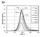


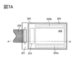


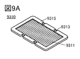


Classifications
-
- H—ELECTRICITY
- H10—SEMICONDUCTOR DEVICES; ELECTRIC SOLID-STATE DEVICES NOT OTHERWISE PROVIDED FOR
- H10K—ORGANIC ELECTRIC SOLID-STATE DEVICES
- H10K50/00—Organic light-emitting devices
- H10K50/80—Constructional details
- H10K50/85—Arrangements for extracting light from the devices
- H10K50/852—Arrangements for extracting light from the devices comprising a resonant cavity structure, e.g. Bragg reflector pair
-
- H—ELECTRICITY
- H10—SEMICONDUCTOR DEVICES; ELECTRIC SOLID-STATE DEVICES NOT OTHERWISE PROVIDED FOR
- H10K—ORGANIC ELECTRIC SOLID-STATE DEVICES
- H10K50/00—Organic light-emitting devices
- H10K50/10—OLEDs or polymer light-emitting diodes [PLED]
- H10K50/11—OLEDs or polymer light-emitting diodes [PLED] characterised by the electroluminescent [EL] layers
-
- C—CHEMISTRY; METALLURGY
- C09—DYES; PAINTS; POLISHES; NATURAL RESINS; ADHESIVES; COMPOSITIONS NOT OTHERWISE PROVIDED FOR; APPLICATIONS OF MATERIALS NOT OTHERWISE PROVIDED FOR
- C09K—MATERIALS FOR MISCELLANEOUS APPLICATIONS, NOT PROVIDED FOR ELSEWHERE
- C09K11/00—Luminescent, e.g. electroluminescent, chemiluminescent materials
- C09K11/06—Luminescent, e.g. electroluminescent, chemiluminescent materials containing organic luminescent materials
-
- G—PHYSICS
- G09—EDUCATION; CRYPTOGRAPHY; DISPLAY; ADVERTISING; SEALS
- G09F—DISPLAYING; ADVERTISING; SIGNS; LABELS OR NAME-PLATES; SEALS
- G09F9/00—Indicating arrangements for variable information in which the information is built-up on a support by selection or combination of individual elements
- G09F9/30—Indicating arrangements for variable information in which the information is built-up on a support by selection or combination of individual elements in which the desired character or characters are formed by combining individual elements
-
- H—ELECTRICITY
- H05—ELECTRIC TECHNIQUES NOT OTHERWISE PROVIDED FOR
- H05B—ELECTRIC HEATING; ELECTRIC LIGHT SOURCES NOT OTHERWISE PROVIDED FOR; CIRCUIT ARRANGEMENTS FOR ELECTRIC LIGHT SOURCES, IN GENERAL
- H05B33/00—Electroluminescent light sources
- H05B33/02—Details
-
- H—ELECTRICITY
- H05—ELECTRIC TECHNIQUES NOT OTHERWISE PROVIDED FOR
- H05B—ELECTRIC HEATING; ELECTRIC LIGHT SOURCES NOT OTHERWISE PROVIDED FOR; CIRCUIT ARRANGEMENTS FOR ELECTRIC LIGHT SOURCES, IN GENERAL
- H05B33/00—Electroluminescent light sources
- H05B33/12—Light sources with substantially two-dimensional radiating surfaces
- H05B33/22—Light sources with substantially two-dimensional radiating surfaces characterised by the chemical or physical composition or the arrangement of auxiliary dielectric or reflective layers
- H05B33/24—Light sources with substantially two-dimensional radiating surfaces characterised by the chemical or physical composition or the arrangement of auxiliary dielectric or reflective layers of metallic reflective layers
-
- H—ELECTRICITY
- H05—ELECTRIC TECHNIQUES NOT OTHERWISE PROVIDED FOR
- H05B—ELECTRIC HEATING; ELECTRIC LIGHT SOURCES NOT OTHERWISE PROVIDED FOR; CIRCUIT ARRANGEMENTS FOR ELECTRIC LIGHT SOURCES, IN GENERAL
- H05B33/00—Electroluminescent light sources
- H05B33/12—Light sources with substantially two-dimensional radiating surfaces
- H05B33/26—Light sources with substantially two-dimensional radiating surfaces characterised by the composition or arrangement of the conductive material used as an electrode
- H05B33/28—Light sources with substantially two-dimensional radiating surfaces characterised by the composition or arrangement of the conductive material used as an electrode of translucent electrodes
-
- H—ELECTRICITY
- H10—SEMICONDUCTOR DEVICES; ELECTRIC SOLID-STATE DEVICES NOT OTHERWISE PROVIDED FOR
- H10K—ORGANIC ELECTRIC SOLID-STATE DEVICES
- H10K50/00—Organic light-emitting devices
- H10K50/80—Constructional details
- H10K50/805—Electrodes
- H10K50/81—Anodes
- H10K50/818—Reflective anodes, e.g. ITO combined with thick metallic layers
-
- H—ELECTRICITY
- H10—SEMICONDUCTOR DEVICES; ELECTRIC SOLID-STATE DEVICES NOT OTHERWISE PROVIDED FOR
- H10K—ORGANIC ELECTRIC SOLID-STATE DEVICES
- H10K50/00—Organic light-emitting devices
- H10K50/80—Constructional details
- H10K50/805—Electrodes
- H10K50/82—Cathodes
- H10K50/828—Transparent cathodes, e.g. comprising thin metal layers
-
- H—ELECTRICITY
- H10—SEMICONDUCTOR DEVICES; ELECTRIC SOLID-STATE DEVICES NOT OTHERWISE PROVIDED FOR
- H10K—ORGANIC ELECTRIC SOLID-STATE DEVICES
- H10K50/00—Organic light-emitting devices
- H10K50/80—Constructional details
- H10K50/85—Arrangements for extracting light from the devices
- H10K50/858—Arrangements for extracting light from the devices comprising refractive means, e.g. lenses
-
- H—ELECTRICITY
- H10—SEMICONDUCTOR DEVICES; ELECTRIC SOLID-STATE DEVICES NOT OTHERWISE PROVIDED FOR
- H10K—ORGANIC ELECTRIC SOLID-STATE DEVICES
- H10K85/00—Organic materials used in the body or electrodes of devices covered by this subclass
- H10K85/30—Coordination compounds
- H10K85/341—Transition metal complexes, e.g. Ru(II)polypyridine complexes
- H10K85/342—Transition metal complexes, e.g. Ru(II)polypyridine complexes comprising iridium
-
- C—CHEMISTRY; METALLURGY
- C09—DYES; PAINTS; POLISHES; NATURAL RESINS; ADHESIVES; COMPOSITIONS NOT OTHERWISE PROVIDED FOR; APPLICATIONS OF MATERIALS NOT OTHERWISE PROVIDED FOR
- C09K—MATERIALS FOR MISCELLANEOUS APPLICATIONS, NOT PROVIDED FOR ELSEWHERE
- C09K2211/00—Chemical nature of organic luminescent or tenebrescent compounds
- C09K2211/10—Non-macromolecular compounds
- C09K2211/1018—Heterocyclic compounds
- C09K2211/1025—Heterocyclic compounds characterised by ligands
- C09K2211/1044—Heterocyclic compounds characterised by ligands containing two nitrogen atoms as heteroatoms
-
- C—CHEMISTRY; METALLURGY
- C09—DYES; PAINTS; POLISHES; NATURAL RESINS; ADHESIVES; COMPOSITIONS NOT OTHERWISE PROVIDED FOR; APPLICATIONS OF MATERIALS NOT OTHERWISE PROVIDED FOR
- C09K—MATERIALS FOR MISCELLANEOUS APPLICATIONS, NOT PROVIDED FOR ELSEWHERE
- C09K2211/00—Chemical nature of organic luminescent or tenebrescent compounds
- C09K2211/18—Metal complexes
- C09K2211/185—Metal complexes of the platinum group, i.e. Os, Ir, Pt, Ru, Rh or Pd
-
- H—ELECTRICITY
- H10—SEMICONDUCTOR DEVICES; ELECTRIC SOLID-STATE DEVICES NOT OTHERWISE PROVIDED FOR
- H10K—ORGANIC ELECTRIC SOLID-STATE DEVICES
- H10K2101/00—Properties of the organic materials covered by group H10K85/00
- H10K2101/10—Triplet emission
-
- H—ELECTRICITY
- H10—SEMICONDUCTOR DEVICES; ELECTRIC SOLID-STATE DEVICES NOT OTHERWISE PROVIDED FOR
- H10K—ORGANIC ELECTRIC SOLID-STATE DEVICES
- H10K2102/00—Constructional details relating to the organic devices covered by this subclass
- H10K2102/301—Details of OLEDs
- H10K2102/302—Details of OLEDs of OLED structures
- H10K2102/3023—Direction of light emission
- H10K2102/3026—Top emission
-
- H—ELECTRICITY
- H10—SEMICONDUCTOR DEVICES; ELECTRIC SOLID-STATE DEVICES NOT OTHERWISE PROVIDED FOR
- H10K—ORGANIC ELECTRIC SOLID-STATE DEVICES
- H10K2102/00—Constructional details relating to the organic devices covered by this subclass
- H10K2102/301—Details of OLEDs
- H10K2102/351—Thickness
-
- H—ELECTRICITY
- H10—SEMICONDUCTOR DEVICES; ELECTRIC SOLID-STATE DEVICES NOT OTHERWISE PROVIDED FOR
- H10K—ORGANIC ELECTRIC SOLID-STATE DEVICES
- H10K50/00—Organic light-emitting devices
- H10K50/80—Constructional details
- H10K50/805—Electrodes
- H10K50/82—Cathodes
-
- H—ELECTRICITY
- H10—SEMICONDUCTOR DEVICES; ELECTRIC SOLID-STATE DEVICES NOT OTHERWISE PROVIDED FOR
- H10K—ORGANIC ELECTRIC SOLID-STATE DEVICES
- H10K85/00—Organic materials used in the body or electrodes of devices covered by this subclass
- H10K85/60—Organic compounds having low molecular weight
- H10K85/615—Polycyclic condensed aromatic hydrocarbons, e.g. anthracene
- H10K85/626—Polycyclic condensed aromatic hydrocarbons, e.g. anthracene containing more than one polycyclic condensed aromatic rings, e.g. bis-anthracene
-
- H—ELECTRICITY
- H10—SEMICONDUCTOR DEVICES; ELECTRIC SOLID-STATE DEVICES NOT OTHERWISE PROVIDED FOR
- H10K—ORGANIC ELECTRIC SOLID-STATE DEVICES
- H10K85/00—Organic materials used in the body or electrodes of devices covered by this subclass
- H10K85/60—Organic compounds having low molecular weight
- H10K85/631—Amine compounds having at least two aryl rest on at least one amine-nitrogen atom, e.g. triphenylamine
- H10K85/633—Amine compounds having at least two aryl rest on at least one amine-nitrogen atom, e.g. triphenylamine comprising polycyclic condensed aromatic hydrocarbons as substituents on the nitrogen atom
-
- H—ELECTRICITY
- H10—SEMICONDUCTOR DEVICES; ELECTRIC SOLID-STATE DEVICES NOT OTHERWISE PROVIDED FOR
- H10K—ORGANIC ELECTRIC SOLID-STATE DEVICES
- H10K85/00—Organic materials used in the body or electrodes of devices covered by this subclass
- H10K85/60—Organic compounds having low molecular weight
- H10K85/631—Amine compounds having at least two aryl rest on at least one amine-nitrogen atom, e.g. triphenylamine
- H10K85/636—Amine compounds having at least two aryl rest on at least one amine-nitrogen atom, e.g. triphenylamine comprising heteroaromatic hydrocarbons as substituents on the nitrogen atom
-
- H—ELECTRICITY
- H10—SEMICONDUCTOR DEVICES; ELECTRIC SOLID-STATE DEVICES NOT OTHERWISE PROVIDED FOR
- H10K—ORGANIC ELECTRIC SOLID-STATE DEVICES
- H10K85/00—Organic materials used in the body or electrodes of devices covered by this subclass
- H10K85/60—Organic compounds having low molecular weight
- H10K85/649—Aromatic compounds comprising a hetero atom
- H10K85/657—Polycyclic condensed heteroaromatic hydrocarbons
- H10K85/6572—Polycyclic condensed heteroaromatic hydrocarbons comprising only nitrogen in the heteroaromatic polycondensed ring system, e.g. phenanthroline or carbazole
-
- H—ELECTRICITY
- H10—SEMICONDUCTOR DEVICES; ELECTRIC SOLID-STATE DEVICES NOT OTHERWISE PROVIDED FOR
- H10K—ORGANIC ELECTRIC SOLID-STATE DEVICES
- H10K85/00—Organic materials used in the body or electrodes of devices covered by this subclass
- H10K85/60—Organic compounds having low molecular weight
- H10K85/649—Aromatic compounds comprising a hetero atom
- H10K85/657—Polycyclic condensed heteroaromatic hydrocarbons
- H10K85/6576—Polycyclic condensed heteroaromatic hydrocarbons comprising only sulfur in the heteroaromatic polycondensed ring system, e.g. benzothiophene
Definitions
- One embodiment of the present invention relates to a light emitting device, a light emitting device, an electronic device, and a lighting device.
- one embodiment of the present invention is not limited thereto. That is, one embodiment of the present invention relates to an object, a method, a manufacturing method, or a driving method. Alternatively, one embodiment of the present invention relates to a process, a machine, a manufacture, or a composition (composition of matter).
- a light-emitting device in which an EL layer is sandwiched between a pair of electrodes has characteristics such as thin and lightweight, high-speed response to an input signal, and low power consumption.
- the applied display is drawing attention as a next-generation flat panel display.
- a light emitting device when a voltage is applied between a pair of electrodes, electrons and holes injected from each electrode are recombined in an EL layer, and a light emitting substance (organic compound) contained in the EL layer is excited, Light is emitted when the excited state returns to the ground state.
- the emission spectrum obtained from a light-emitting substance is unique to the light-emitting substance, and by using different kinds of organic compounds as the light-emitting substance, light-emitting devices with various emission colors can be obtained.
- the light emitting device having a microcavity structure it is preferable to use an electrode material having a high reflectance for the reflective electrode and the semitransparent semireflective electrode.
- materials with high reflectance are used to increase the film thickness in order to further increase the reflectance. If the thickness is increased, a part of light is absorbed by the semi-transmissive-semi-reflective electrode, resulting in a large loss, which causes a problem that luminous efficiency is reduced. Therefore, in a light emitting device that emits light in the normal visible light region, the efficiency has been improved by making the film thickness of the semi-transmissive semi-reflective electrode thinner.
- a light-emitting device having a microcavity structure which is capable of further improving light-emission efficiency. Further, in a light emitting device having a microcavity structure, a novel light emitting device capable of improving the reliability of the element is provided.
- a light emitting device having a microcavity structure when the light emitted from the EL layer is in the near infrared region (around 750 nm to 1000 nm), gold (Au), silver (Ag), copper (Cu ) Is used for the light in the near-infrared region, which is higher than the light in the visible region, in the specific film thickness range where the film thickness of the semi-transmissive/semi-reflective electrode is increased.
- the reflective electrode has a reflectance of 40% or more and 100% or less for visible light (light having a wavelength of 400 nm or more and less than 750 nm) or near infrared light (light having a wavelength of 750 nm or more and 1000 nm or less).
- the semi-transmissive/semi-reflective electrode has a reflectance for visible light or near infrared light of 20% or more and 80% or less, preferably 40% or more and 70% or less. ..
- a material having high reflectance is used for the reflective electrode of the light emitting device or both the reflective electrode and the semi-transmissive semi-reflective electrode.
- the thickness of the electrode in the above range as compared with the conventional one, it is possible to form an electrode having high reflectance while suppressing the absorption of light. Since the resistance can be reduced, a light emitting device with high emission efficiency and reduced driving voltage can be obtained.
- One embodiment of the present invention has an EL layer between a first electrode and a second electrode, the first electrode is a reflective electrode, and the second electrode is light (especially near-infrared region (750 nm). It is a semi-transmissive semi-reflective electrode having both functions of transmitting and reflecting (light of 1000 nm or less)), which emits light in the near infrared region from the EL layer, and one or both of the first electrode and the second electrode. Is a light emitting device that exhibits a higher reflectance for light in the near infrared region (for example, 850 nm light) than light in the visible light region (400 nm or more and less than 750 nm) (for example, light with a wavelength of 500 nm).
- Another embodiment of the present invention has an EL layer between a first electrode and a second electrode, the first electrode is a reflective electrode, and the second electrode is light (especially near-red light).
- a semi-transmissive semi-reflective electrode having both functions of transmitting and reflecting an outer region (light of 750 nm or more and 1000 nm or less), which emits light in the near infrared region from the EL layer, and emits light in the near infrared region of the first electrode and the second electrode.
- the electrode is a light emitting device having a film thickness of 20 nm or more and 60 nm or less, preferably 30 nm or more and 60 nm or less, more preferably 40 nm or more and 50 nm or less.
- an organic layer is preferably in contact with the second electrode, and the organic layer preferably has a refractive index of 1.7 or more.
- the thickness of the organic layer is 80 nm or more and 160 nm or less, more preferably 80 nm or more and 120 nm or less.
- Another embodiment of the present invention has an EL layer between a first electrode and a second electrode, the first electrode is a reflective electrode, and the second electrode is a semi-transmissive semi-reflective electrode.
- the EL layer has a light emitting substance that exhibits a light emission peak in the near infrared region (a wavelength range of 750 nm to 1000 nm), and the light emitted by the EL layer has a wavelength longer than that of the light emitting substance. Is a device.
- the first electrode or the second electrode preferably contains at least one of gold (Au), silver (Ag), and copper (Cu).
- the first electrode have a reflectance of 90% or more with respect to light having a wavelength of 850 nm.
- the second electrode preferably exhibits a reflectance of 90% or more with respect to light having a wavelength of 850 nm.
- the light-emitting substance is preferably a phosphorescent light-emitting substance.
- the light-emitting substance is preferably an organometallic complex represented by the general formula (G1).
- R 1 to R 11 each independently represent hydrogen or an alkyl group having 1 to 6 carbon atoms, and at least two of R 1 to R 4 have 1 to 6 carbon atoms.
- one embodiment of the present invention is not only a light-emitting device including the above-described light-emitting device, but also a light-emitting device or an electronic device to which the light-emitting device is applied (specifically, the light-emitting device or the light-emitting device, a connection terminal, or an operation key.
- the electronic device having a) and the lighting device are also included in the category. Therefore, the light-emitting device in this specification refers to an image display device or a light source (including a lighting device).
- a connector such as an FPC (Flexible Printed Circuit) or TCP (Tape Carrier Package) is attached to the light emitting device, a module in which a printed wiring board is provided in front of the TCP, or a COG (Chip On Glass) to the light emitting device. All modules in which an IC (Integrated Circuit) is directly mounted by the method are included in the light emitting device.
- FPC Flexible Printed Circuit
- TCP Transmission Carrier Package
- a novel light-emitting device capable of improving light-emission efficiency as compared with conventional light-emitting devices can be provided. Further, according to one embodiment of the present invention, in a light-emitting device having a microcavity structure, a novel light-emitting device that can improve element reliability can be provided.
- FIG. 1A and 1B are views for explaining the structure of a light emitting device.
- FIG. 2 is a diagram for explaining the structure of the light emitting device.
- FIG. 3 is a diagram showing a simulation result of the reflectance of the electrode material.
- FIG. 4 is a diagram showing simulation results of EL emission spectra emitted in the front direction.
- FIG. 5 is a diagram showing a simulation result of the light extraction efficiency of the EL emission spectrum emitted in the front direction.
- FIG. 6 is a diagram showing a simulation result of the peak intensity of the EL emission spectrum emitted in the front direction.
- 7A and 7B are diagrams illustrating a light emitting device.
- 8A, 8B, 8C, 8D, 8E, 8F, and 8G are diagrams illustrating electronic devices.
- FIG. 9A, 9B, and 9C are diagrams illustrating electronic devices. 10A and 10B are diagrams for explaining an automobile. 11A and 11B are diagrams illustrating a lighting device.
- FIG. 12 is a diagram illustrating a light emitting device.
- FIG. 13 is a diagram showing current density-radiation emittance characteristics of the light emitting device 1 and the light emitting device 2.
- FIG. 14 is a diagram showing voltage-current density characteristics of the light emitting device 1 and the light emitting device 2.
- FIG. 15 is a diagram showing current density-external quantum efficiency characteristics of the light emitting device 1 and the light emitting device 2.
- FIG. 16 is a diagram showing voltage-radiation emittance characteristics of the light emitting device 1 and the light emitting device 2.
- FIG. 17 is a diagram showing the spectral radiance of the light emitting device 1 and the light emitting device 2.
- FIG. 18 is an emission spectrum of [Ir(dmdpbq) 2 (dpm)], which is an organometallic complex.
- FIG. 19 is a diagram showing the viewing angle dependence of the light emitting device 1 and the light emitting device 2.
- FIG. 20 is a diagram showing a reliability test of the light emitting device 1 and the light emitting device 2.
- FIG. 1 shows an example of a light emitting device having an EL layer including a light emitting layer between a pair of electrodes.
- the EL layer 103 is sandwiched between the first electrode 101 and the second electrode 102.
- the EL layer 103 includes, for example, a hole (hole) injection layer 111, a hole (hole) transport layer 112, a light emitting layer 113, an electron transport layer 114, and an electron injection layer when the first electrode 101 serves as an anode.
- the functional layer 115 has a structure in which layers are sequentially stacked.
- the light-emitting device which is one embodiment of the present invention has a micro-optical resonator (microcavity) structure, and one of a pair of electrodes is a reflective electrode and the other is a semi-transmissive/semi-reflective electrode. It has a structure capable of amplifying light having a wavelength corresponding to the distance between electrodes (also referred to as cavity length or optical path length) by repeating reflection.
- the cavity length can be changed by adjusting the thickness of the EL layer and the electrode.
- a transparent electrode such as ITO can be used.
- the optical path length can be controlled by adjusting the thickness of the carrier transport layer or the carrier injection layer.
- the light emitting direction of the light emitting device may be a top emission structure or a bottom emission structure.
- the first electrode 101 has a reflective property and the second electrode 102 has a semi-transmissive property having both a light-transmitting property and a light-reflecting function. Has semi-reflectivity.
- the first electrode 101 is a reflective electrode, and the reflectance of the electrode with respect to visible light or near infrared light is 40% to 100% inclusive, preferably 70% to 100% inclusive.
- the second electrode 102 is a semi-transmissive/semi-reflective electrode, and the reflectance of the electrode with respect to visible light or near infrared light is 20% or more and 80% or less, preferably 40% or more and 70% or less. Moreover, it is preferable that the resistivity of each of these electrodes is 1 ⁇ 10 ⁇ 2 ⁇ cm or less. Therefore, light is emitted from the interface (reflection area) of the first electrode 101 with the EL layer 103 to the light emitting layer 113 (light emission area) and the interface (reflection area) of the second electrode 102 with the EL layer 103.
- the intensity of desired light (wavelength) emitted from the light emitting layer 113 can be increased by adjusting the optical distance to the layer 113 (light emitting region).
- an organic compound layer having a molecular weight of 300 or more and 1200 or less is formed on a surface of the second electrode 102 (semi-transmissive/semi-reflective electrode) opposite to the surface facing the reflective electrode ( It is preferable that the organic cap layer 105) is formed.
- the organic cap layer 105 is preferably an organic compound layer having a molecular weight of 300 or more and 1200 or less.
- an organic material having conductivity is preferable.
- the second electrode 102 is a semi-transmissive/semi-reflective electrode, it is necessary to reduce the film thickness in order to maintain translucency to some extent, which may deteriorate the conductivity.
- the organic cap layer 105 by using a material having conductivity for the organic cap layer 105, it is possible to secure conductivity while improving the light extraction efficiency and improve the yield of manufacturing the light emitting element. It should be noted that an organic compound that has little absorption in a desired wavelength region of light can be preferably used.
- the organic compound used for the EL layer 103 can also be used for the organic cap layer 105. In this case, since the organic cap layer 105 can be formed in the film forming apparatus or the film forming chamber in which the EL layer 103 is formed, the organic cap layer 105 can be easily formed.
- the optical distance from the interface (reflection area) of the first electrode 101 to the EL layer 103 to the light emitting layer 113 (light emission area) is the light emission from the interface (reflection area) of the first electrode 101 to the EL layer 103. It is represented by the product of the distance to the layer 113 (light emitting region) and the refractive index.
- the optical distance from the interface (reflection area) of the second electrode 102 to the EL layer 103 to the light emitting layer 113 (light emission area) is the light emission from the interface (reflection area) of the second electrode 102 to the EL layer 103. It is represented by the product of the distance to the layer 113 (light emitting region) and the refractive index.
- the film thickness of the first electrode 101 is adjusted to
- the desired light emitted from the light-emitting layer 113 ((m is a natural number, ⁇ is the wavelength of the desired light, respectively) is adjusted by adjusting the optical distance from the second electrode 102 to around m ⁇ /2 (where m is a natural number and ⁇ is the wavelength of the desired light, respectively). Wavelength) can be increased.
- any one or more of the hole injection layer 111, the hole transport layer 112, the electron transport layer 114, and the electron injection layer 115 can be obtained.
- the intensity of light (wavelength) can be increased.
- a light emitting device having a bottom emission structure may be used in which the first electrode 101 is a semi-transmissive/semi-reflective electrode and the second electrode 102 is a reflective electrode.
- the light-emitting device which is one embodiment of the present invention has a structure in which one of the first electrode 101 and the second electrode 102 is a semi-transmissive/semi-reflective electrode and the other is a reflective electrode. Is preferable for obtaining high luminous efficiency.
- the following materials can be appropriately combined and used.
- a metal, an alloy, an electrically conductive compound, a mixture thereof, or the like can be used as appropriate.
- In-Sn oxide also referred to as ITO
- In-Si-Sn oxide also referred to as ITSO
- In-Zn oxide and In-W-Zn oxide can be given.
- elements belonging to Group 1 or Group 2 of the Periodic Table of Elements for example, lithium (Li), cesium (Cs), calcium (Ca), strontium (Sr)), europium (Eu), ytterbium
- Yb ytterbium
- Yb rare earth metal
- an alloy containing a proper combination thereof, or other graphene can be used.
- materials having high reflectance such as gold (Au), silver (Ag), copper (Cu), and aluminum (Al), have different reflectance with respect to the wavelength of light.
- a simulation was performed to show the behavior. The result is shown in FIG.
- the reflectance of silver (Ag) is high with almost no effect on the light of different wavelengths, but the light in the visible light region (near 400 nm to 750 nm) is less than 750 nm. It was found that a higher reflectance was exhibited for light in the near-infrared region of 750 nm or more (near 750 nm to 1000 nm) as compared with.
- gold (Au) and copper (Cu) show low reflectance with respect to light in the visible light region (near 400 nm to 750 nm) of less than 750 nm, but near infrared region of 750 nm or more (750 nm to It was found that a high reflectance is exhibited for light of around 1000 nm).
- Aluminum (Al) which is often used as a material for a reflective electrode of a light emitting device, has a high reflectance for light in the visible light region, but has a long wavelength of 750 nm or more, that is, light in the near infrared region. As a result, the reflectance was decreased.
- the wavelength of light emitted from the light emitting layer 113 of the light emitting device is long wavelength light of 750 nm or more
- gold (Au), silver (Ag) is used as the electrode material of the reflective electrode or the semi-transmissive/semi-reflective electrode.
- copper (Cu) or copper (Cu) are preferable because they show higher reflectance for light having a wavelength of 850 nm than light having a wavelength of 500 nm.
- these electrode materials are preferable because they show a reflectance of 90% or more at a wavelength of 850 nm.
- the light emitting device 0 having the top emission structure shown in FIG. 2, as a model, the change in the EL emission spectrum emitted in the front direction with the change in the film thickness of the second electrode 102 which is a semi-transmissive/semi-reflective electrode. , A simulation was performed. The results are shown in Fig. 4.
- the element structure of the light emitting device 0 is shown in Table 1 below. Since the light emitting layer 113 of the light emitting device 0 has an organic metal complex [Ir(dmdpbq) 2 (dpm)] as a light emitting substance, the light obtained from the light emitting layer 113 is [Ir(dmdpbq) 2 (dpm)].
- the hole injecting layer 111 and the electron injecting layer are formed so that the emission intensity near the wavelength of 800 nm becomes maximum.
- the film thicknesses of 115 and the organic cap layer 105 are appropriately adjusted.
- FIG. 5 shows the relationship between the area of the EL emission spectrum in the front direction and the film thickness of the second electrode 102 in the wavelength range of the simulation shown in FIG.
- the thickness of the second electrode 102 is preferably 20 nm or more and 60 nm or less, more preferably 30 nm or more and 60 nm or less, and further preferably 30 nm or more and 50 nm or less.
- the thickness of the organic cap layer 105 is preferably 80 nm or more and 160 nm or less, and more preferably 80 nm or more and 120 nm or less. Do you get it.
- a sputtering method or a vacuum evaporation method can be used for manufacturing these electrodes.
- the hole-injection layer 111 is a layer for injecting holes from the first electrode 101 which is an anode into the EL layer 103, and is a layer containing an organic acceptor material or a material having a high hole-injection property.
- the organic acceptor material is a material capable of generating holes in the organic compound by performing charge separation between the LUMO level value and another organic compound having a close HOMO level value. is there. Therefore, as the organic acceptor material, a compound having an electron withdrawing group (halogen group or cyano group) such as a quinodimethane derivative, a chloranil derivative, or a hexaazatriphenylene derivative can be used.
- an electron withdrawing group halogen group or cyano group
- HAT-CN is particularly preferable because it has a high acceptor property and its film quality is stable against heat.
- the [3]radialene derivative is preferable because it has a very high electron-accepting property, and specifically, ⁇ , ⁇ ′, ⁇ ′′-1,2,3-cyclopropanetriylidenetris[4-cyano- 2,3,5,6-Tetrafluorobenzeneacetonitrile], ⁇ , ⁇ ′, ⁇ ′′-1,2,3-cyclopropanetriylidene tris[2,6-dichloro-3,5-difluoro-4-( Trifluoromethyl)benzeneacetonitrile], ⁇ , ⁇ ′, ⁇ ′′-1,2,3-cyclopropanetriylidenetris[2,3,4,5,6-pentafluorobenzeneacetonitrile] and the like can be used. ..
- Examples of the material having a high hole injecting property include transition metal oxides such as molybdenum oxide, vanadium oxide, ruthenium oxide, tungsten oxide, and manganese oxide.
- a phthalocyanine-based compound such as phthalocyanine (abbreviation: H 2 Pc) or copper phthalocyanine (abbreviation: CuPC) can be used.
- low molecular weight compounds such as 4,4′,4′′-tris(N,N-diphenylamino)triphenylamine (abbreviation: TDATA), 4,4′,4′′-tris [N-(3-methylphenyl)-N-phenylamino]triphenylamine (abbreviation: MTDATA), 4,4′-bis[N-(4-diphenylaminophenyl)-N-phenylamino]biphenyl (abbreviation: DPAB), 4,4'-bis(N- ⁇ 4-[N'-(3-methylphenyl)-N'-phenylamino]phenyl ⁇ -N-phenylamino)biphenyl (abbreviation: DNTPD), 1,3 ,5-Tris[N-(4-diphenylaminophenyl)-N-phenylamino]benzene (abbreviation: DPA3B), 3-[N-(9-phen
- high molecular compounds oligomers, dendrimers, polymers, etc.
- poly(N-vinylcarbazole) abbreviation: PVK
- poly(4-vinyltriphenylamine) abbreviation: PVTPA
- poly[N-(4 - ⁇ N'-[4-(4-diphenylamino)phenyl]phenyl-N'-phenylamino ⁇ phenyl)methacrylamide] abbreviation: PTPDMA
- poly[N,N'-bis(4-butylphenyl)- [N,N′-bis(phenyl)benzidine] abbreviation: Poly-TPD) or the like can be used.
- PEDOT/PSS poly(3,4-ethylenedioxythiophene)/poly(styrenesulfonic acid)
- PAni/PSS polyaniline/poly(styrenesulfonic acid)
- a composite material containing a hole transporting material and an acceptor material can also be used.
- electrons are extracted from the hole-transporting material by the acceptor material, holes are generated in the hole-injection layer 111, and holes are injected into the light-emitting layer 113 through the hole-transport layer 112.
- the hole-injection layer 111 may be formed as a single layer formed of a composite material containing a hole-transporting material and an acceptor material (electron-accepting material), but the hole-transporting material and the acceptor material ( Electron-accepting material) may be laminated in different layers.
- the hole-transporting material a substance having a hole mobility of 1 ⁇ 10 ⁇ 6 cm 2 /Vs or higher is preferable. Note that any substance other than the above substances can be used as long as it has a property of transporting more holes than electrons.
- a material having a high hole transporting property such as a ⁇ -electron excess type heteroaromatic compound is preferable.
- a ⁇ -electron excess heteroaromatic compound an aromatic amine skeleton, an aromatic amine compound (having a triarylamine skeleton), a carbazole compound having a carbazole skeleton (without a triarylamine skeleton), Examples thereof include a thiophene compound (compound having a thiophene skeleton), a furan compound (compound having a furan skeleton), and the like.
- aromatic amine compound 4,4′-bis[N-(1-naphthyl)-N-phenylamino]biphenyl (abbreviation: NPB or ⁇ -NPD), N,N′-bis(3-) Methylphenyl)-N,N′-diphenyl-[1,1′-biphenyl]-4′4′-diamine (abbreviation: TPD), 4,4′-bis[N-(spiro-9,9′-bifluorene 2-yl)-N-phenylamino]biphenyl (abbreviation: BSPB), 4-phenyl-4′-(9-phenylfluoren-9-yl)triphenylamine (abbreviation: BPAFLP), 4-phenyl-3′ -(9-Phenylfluoren-9-yl)triphenylamine (abbreviation: mBPAFLP), N-(9,9-dimethyl-9H
- aromatic amine compound having a carbazolyl group 4-phenyl-4′-(9-phenyl-9H-carbazol-3-yl)triphenylamine (abbreviation: PCBA1BP), N-(4-biphenyl)- N-(9,9-dimethyl-9H-fluoren-2-yl)-9-phenyl-9H-carbazol-3-amine (abbreviation: PCBiF), N-(1,1'-biphenyl-4-yl)- N-[4-(9-phenyl-9H-carbazol-3-yl)phenyl]-9,9-dimethyl-9H-fluoren-2-amine (abbreviation: PCBBiF), 4,4'-diphenyl-4'' -(9-Phenyl-9H-carbazol-3-yl)triphenylamine (abbreviation: PCBBi1BP), 4-(1-naphthyl)-4'-(9-phenyl-9H,
- PCBFF N-[4-(9-phenyl-9H-carbazole -3-yl)phenyl]-N-[4-(1-naphthyl)phenyl]-9,9'-spirobi(9H-fluorene)-2-amine
- PCBNBF N-[4-(9- Phenyl-9H-carbazol-3-yl)phenyl]-9,9-dimethyl-N-[4-(1-naphthyl)phenyl]-9H-fluoren-2-amine
- PCBNBF N-phenyl-N -[4-(9-phenyl-9H-carbazol-3-yl)phenyl]spiro-9,9'-bifluoren-2-
- PCzPCA2 3-[N-(1-naphthyl)-N-(9-phenylcarbazol-3-yl)amino]-9-phenylcarbazole
- PCzPCN1 3-[N-(4-diphenylaminophenyl)-N-phenylamino]-9-phenylcarbazole
- PCzDPA1 3,6-bis[N-(4-diphenylaminophenyl) -N-phenylamino]-9-phenylcarbazole
- PCzDPA2 3,6-bis[N-(4-diphenylaminophenyl)-N-(1-naphthyl)amino]-9-phenylcarbazole
- PCzTPN2 2-[N-(9
- examples of the carbazole compound include 3-[4-(9-phenanthryl)-phenyl]-9-phenyl-9H-carbazole (abbreviation: PCPPn) and 3-[4-.
- PCPN 1,3-bis(N-carbazolyl)benzene
- CBP 4,4′-di(N-carbazolyl) Biphenyl
- CzTP 3,6-bis(3,5-diphenylphenyl)-9-phenylcarbazole
- TCPB 1,3,5-tris[4-(N-carbazolyl)phenyl]benzene
- TCPB 9-[4-(10-phenyl-9-anthracenyl)phenyl]-9H-carbazole
- CzPA 9-[4-(10-phenyl-9-anthracenyl)phenyl]-9H-carbazole
- PCCP 3,3′-bis(9-phenyl-9H-carbazole)
- PCCP which is a bicarbazole derivative (eg, 3,3′-bicarbazole derivative), 9-(1,1′-biphenyl -3-yl)-9'-(1,1'-biphenyl-4-yl)-9H,9'H-3,3'-bicarbazole (abbreviation: mBPCCBP), 9-(2-naphthyl)-9 Examples thereof include'-phenyl-9H,9'H-3,3'-bicarbazole (abbreviation: ⁇ NCCP).
- thiophene compound compound having a thiophene skeleton
- 1,3,5-tri(dibenzothiophen-4-yl)benzene abbreviation: DBT3P-II
- 2,8-diphenyl-4-[4- (9-Phenyl-9H-fluoren-9-yl)phenyl]dibenzothiophene abbreviation: DBTFLP-III
- furan compound compound having a furan skeleton
- 4,4′,4′′-(benzene-1,3,5-triyl)tri(dibenzofuran) abbreviation: DBF3P-II
- 4- ⁇ 3-[3-(9-phenyl-9H-fluoren-9-yl)phenyl]phenyl ⁇ dibenzofuran abbreviation: mmDBFFLBi-II
- poly(N-vinylcarbazole) (abbreviation: PVK), poly(4-vinyltriphenylamine) (abbreviation: PVTPA), poly[N-(4- ⁇ N'-[4-(4-diphenyl) Amino)phenyl]phenyl-N′-phenylamino ⁇ phenyl)methacrylamide] (abbreviation: PTPDMA), poly[N,N′-bis(4-butylphenyl)-N,N′-bis(phenyl)benzidine]( A polymer compound such as abbreviation: Poly-TPD) can be used as the hole transporting material.
- PVK poly(N-vinylcarbazole)
- PVTPA poly(4-vinyltriphenylamine)
- PTPDMA poly[N-(4- ⁇ N'-[4-(4-diphenyl) Amino)phenyl]phenyl-N′-phenylamino ⁇ phenyl)
- the hole-transporting material is not limited to the above, and various known materials may be used alone or in combination of two or more as a hole-transporting material.
- an oxide of a metal belonging to Groups 4 to 8 in the periodic table can be used.
- Specific examples include molybdenum oxide, vanadium oxide, niobium oxide, tantalum oxide, chromium oxide, tungsten oxide, manganese oxide, and rhenium oxide.
- molybdenum oxide is particularly preferable because it is stable in the air, has low hygroscopicity, and is easy to handle.
- the organic acceptor mentioned above can also be used.
- the hole injection layer 111 can be formed by using various known film formation methods, for example, a vacuum evaporation method.
- the hole transport layer 112 is a layer that transports the holes injected from the first electrode 101 to the light emitting layer 113 by the hole injection layer 111.
- the hole-transporting layer 112 is a layer containing a hole-transporting material. Therefore, the hole-transporting layer 112 can use a hole-transporting material that can be used for the hole-injecting layer 111.
- the same organic compound as the hole-transporting layer 112 is preferably used for the light-emitting layer 113.
- the same organic compound for the hole transport layer 112 and the light emitting layer 113 holes can be efficiently transported from the hole transport layer 112 to the light emitting layer 113.
- the light emitting layer 113 is a layer containing a light emitting substance (organic compound).
- a light-emitting substance that can be used for the light-emitting layer 113, such as a light-emitting substance that converts singlet excitation energy into light emission in a visible light region (eg, a fluorescent light-emitting substance) or triplet excitation energy that is visible light.
- a light-emitting substance eg, a phosphorescent light-emitting substance or a TADF material which is converted into light emission in a region can be used.
- the emission layer when light having an emission peak in a wavelength range of 750 nm to 1000 nm is emitted from the EL layer, the emission layer emits light in a wavelength range of 750 nm to 1000 nm.
- an organic compound having a peak such as an organometallic complex.
- a phthalocyanine compound central metal: aluminum, zinc, etc.
- a naphthalocyanine compound central metal: nickel
- a quinone compound a diimonium compound, an azo compound, etc.
- organometallic complex having an emission peak in a wavelength range of 750 nm to 1000 nm an organometallic complex represented by the following general formula can be given.
- R 1 to R 11 each independently represent hydrogen or an alkyl group having 1 to 6 carbon atoms, and at least two of R 1 to R 4 have 1 to 6 carbon atoms. At least two of R 5 to R 9 represent an alkyl group having 1 to 6 carbon atoms, X represents a substituted or unsubstituted benzene ring or naphthalene ring, and n is 2 or 3 and L represents a monoanionic ligand.
- the alkyl group having 1 to 6 carbon atoms as the alkyl group having 1 to 6 carbon atoms, a methyl group, an ethyl group, a propyl group, an isopropyl group, a butyl group, a sec-butyl group, an isobutyl group, a tert-butyl group, a pentyl group, Isopentyl group, sec-pentyl group, tert-pentyl group, neopentyl group, hexyl group, isohexyl group, 3-methylpentyl group, 2-methylpentyl group, 2-ethylbutyl group, 1,2-dimethylbutyl group, 2,3 A dimethylbutyl group and the like.
- the substituent is an alkyl group having 1 to 6 carbon atoms.
- the above description can be applied to the alkyl group having 1 to 6 carbon atoms.
- Examples of the monoanionic ligand include a monoanionic bidentate chelate ligand having a ⁇ -diketone structure, a monoanionic bidentate chelate ligand having a carboxyl group, and a monoanionic bidentate having a phenolic hydroxyl group.
- Bidentate chelate ligands, monoanionic bidentate chelate ligands in which the two coordinating elements are both nitrogen, bidentate ligands that form a metal-carbon bond with iridium by cyclometallation, etc. Can be mentioned.
- the monoanionic ligand is preferably any one of formulas (L1) to (L8).
- R 51 to R 89 are each independently hydrogen or a substituted or unsubstituted alkyl group having 1 to 6 carbon atoms, a halogeno group, a vinyl group, a substituted or unsubstituted carbon group.
- a 1 to A 13 each independently represent sp 2 hybrid carbon bonded to nitrogen or hydrogen, or sp 2 hybrid carbon having a substituent, and the substituent is an alkyl group having 1 to 6 carbon atoms.
- organometallic complex represented by the general formula (G1) include organometallic complexes represented by structural formulas (100) to (107). However, the present invention is not limited to these.
- the light-emitting layer 113 a substance other than the above, which emits a light-emitting color such as blue, purple, blue-violet, green, yellow-green, yellow, orange, or red can be used as appropriate.
- the light-emitting layer 113 includes a light-emitting substance (guest material) and one or more kinds of organic compounds (host material or the like). However, it is preferable to use a substance having an energy gap larger than that of the light-emitting substance (guest material) for the organic compound (host material or the like) used here.
- a hole transporting material that can be used in the hole transporting layer 112 described above and an electron transporting property that can be used in the electron transporting layer 114 described below. Examples include organic compounds such as materials.
- the light-emitting layer 113 has a structure including a first organic compound, a second organic compound, and a light-emitting substance
- an electron-transporting material is used as the first organic compound and a positive organic compound is used as the second organic compound.
- a hole-transporting material can be used, and a phosphorescent material, a fluorescent material, a TADF material, or the like can be used as a light-emitting material.
- the first organic compound and the second organic compound are a combination that forms an exciplex.
- the light emitting layer 113 may have a plurality of light emitting layers containing different light emitting substances so that different light emitting colors are exhibited (for example, white light emission obtained by combining light emitting colors having complementary colors). good.
- one light emitting layer may have a plurality of different light emitting substances.
- examples of the light-emitting substance that can be used for the light-emitting layer 113 include the following.
- examples of the light-emitting substance that converts singlet excitation energy into light emission include substances that emit fluorescence (fluorescent light-emitting substances).
- pyrimidine derivatives, phenanthrene derivatives, naphthalene derivatives and the like include derivatives, pyrimidine derivatives, phenanthrene derivatives, naphthalene derivatives and the like.
- the pyrene derivative is preferable because it has a high emission quantum yield.
- pyrene derivative examples include N,N'-bis(3-methylphenyl)-N,N'-bis[3-(9-phenyl-9H-fluoren-9-yl)phenyl]pyrene-1,6. -Diamine (abbreviation: 1,6mMemFLPAPrn), N,N'-diphenyl-N,N'-bis[4-(9-phenyl-9H-fluoren-9-yl)phenyl]pyrene-1,6-diamine (abbreviation) : 1,6FLPAPrn), N,N'-bis(dibenzofuran-2-yl)-N,N'-diphenylpyrene-1,6-diamine (abbreviation: 1,6FrAPrn), N,N'-bis(dibenzothiophene -2-yl)-N,N'-diphenylpyrene-1,6-diamine (abbreviation: 1,6ThAPrn
- the light-emitting substance (fluorescent light-emitting substance) that can be used for the light-emitting layer 113 and that converts singlet excitation energy into light emission is not limited to the above-described fluorescent light-emitting substance that emits an emission color (emission peak) in the visible light region. It is also possible to use a fluorescent light-emitting substance that exhibits an emission color (emission peak) in a part of the near-infrared light region (for example, a material that emits red light and has a wavelength of 800 nm or more and 950 nm or less).
- a luminescent substance that converts triplet excitation energy into luminescence for example, a substance that emits phosphorescence (phosphorescent luminescent substance) or a thermally activated delayed fluorescence (TADF) material that exhibits thermally activated delayed fluorescence is used.
- phosphorescence phosphorescent luminescent substance
- TADF thermally activated delayed fluorescence
- examples of the phosphorescent light-emitting substance that is a light-emitting substance that converts triplet excitation energy into light emission include an organometallic complex, a metal complex (platinum complex), and a rare earth metal complex. These show different emission colors (emission peaks) depending on the substances, and are appropriately selected and used as necessary.
- examples of the material exhibiting a luminescent color (emission peak) in the visible light region include the following materials.
- a phosphorescent substance that exhibits blue or green and has a peak wavelength of an emission spectrum of 450 nm to 570 nm e.g., 450 nm to 495 nm in the case of blue, and 495 nm to 570 nm in the case of green
- 450 nm to 495 nm in the case of blue, and 495 nm to 570 nm in the case of green is preferable.
- the following substances may be mentioned.
- Examples of the phosphorescent substance that exhibits green, yellowish green, or yellow and has a peak wavelength of an emission spectrum of 495 nm to 590 nm inclusive include the following substances. (For example, in the case of green, 495 nm or more and 570 nm or less, in the case of yellow-green, 530 nm or more and 570 nm or less, and in the case of yellow, 570 nm or more and 590 nm or less are preferable.)
- tris(4-methyl-6-phenylpyrimidinato)iridium(III) (abbreviation: [Ir(mppm) 3 ]), tris(4-t-butyl-6-phenylpyrimidinato)iridium(III) (Abbreviation: [Ir(tBuppm) 3 ]), (acetylacetonato)bis(6-methyl-4-phenylpyrimidinato)iridium(III) (abbreviation: [Ir(mppm) 2 (acac)]), Acetylacetonato)bis(6-tert-butyl-4-phenylpyrimidinato)iridium(III) (abbreviation: [Ir(tBuppm) 2 (acac)]), (acetylacetonato)bis[6-(2- Norbornyl)-4-phenylpyrimidinato]iridium (III) (abbreviation: [Ir(nbppm) 2
- Iridium (III) acetylacetonate (abbreviation: [Ir(bzq) 2 (acac)]), tris(benzo[h]quinolinato) iridium (III) (abbreviation: [I r (bzq) 3]), tris (2-phenylquinolinato -N, C 2 ') iridium (III) (abbreviation: [Ir (pq) 3] ), bis (2-phenylquinolinato--N, C 2 ′ ) Iridium(III) acetylacetonate (abbreviation: [Ir(pq) 2 (acac)]), bis[2-(2-pyridinyl- ⁇ N)phenyl- ⁇ C][2-(4-phenyl-2-pyridinyl) - ⁇ N)phenyl- ⁇ C]iridium(III) (abbreviation: [Ir(ppy) 2 (4dppy)]), bis[2-(2-pyridinyl
- Examples of the phosphorescent substance that exhibits yellow, orange, or red and has a peak wavelength of an emission spectrum of 570 nm or more and 750 nm or less include the following substances. (For example, preferably 570 nm or more and 590 nm or less for yellow, 590 nm or more and 620 nm or less for orange, and 600 nm or more and 750 nm or less for red.)
- a TADF material that is a light-emitting substance that converts triplet excitation energy into light emission
- the following materials can be used.
- a TADF material is a material that can up-convert the triplet excited state into a singlet excited state (reverse intersystem crossing) with a small amount of thermal energy and efficiently exhibit light emission (fluorescence) from the singlet excited state. That is.
- the energy difference between the triplet excitation level and the singlet excitation level is 0 eV or more and 0.2 eV or less, preferably 0 eV or more and 0.1 eV or less.
- the delayed fluorescence in the TADF material refers to light emission that has a spectrum similar to that of normal fluorescence but has a significantly long lifetime. Its life is 1 ⁇ 10 ⁇ 6 seconds or more, preferably 1 ⁇ 10 ⁇ 3 seconds or more.
- the TADF material include fullerene and its derivatives, acridine derivatives such as proflavin, and eosin.
- a metal-containing porphyrin containing magnesium (Mg), zinc (Zn), cadmium (Cd), tin (Sn), platinum (Pt), indium (In), palladium (Pd), or the like can be given.
- the metal-containing porphyrin for example, protoporphyrin-tin fluoride complex (abbreviation: SnF 2 (Proto IX)), mesoporphyrin-tin fluoride complex (abbreviation: SnF 2 (Meso IX)), hematoporphyrin-tin fluoride.
- SnF 2 Hemato IX
- SnF 2 coproporphyrin tetramethyl ester-tin fluoride complex
- SnF 2 Copro III-4Me
- SnF 2 octaethylporphyrin-tin fluoride complex
- SnF 2 (OEP) Ethioporphyrin-tin fluoride complex
- PtCl 2 OEP octaethylporphyrin-platinum chloride complex
- a substance in which the ⁇ -electron excess heteroaromatic ring and the ⁇ -electron deficient heteroaromatic ring are directly bound to each other has both a donor property of the ⁇ -electron excess heteroaromatic ring and an acceptor property of the ⁇ -electron deficient heteroaromatic ring. It is particularly preferable because the energy difference between the singlet excited state and the triplet excited state becomes small.
- a light-emitting substance as described above a light-emitting substance that changes singlet excitation energy into light emission in the visible light region (for example, a fluorescent light-emitting substance)) or a light-emitting substance that changes triplet excitation energy into light emission in the visible light region (for example, in the case of using a phosphorescent light emitting material, a TADF material, etc.), in addition to these light emitting materials (organic compounds), it is preferable to combine with Is preferably used.
- an organic compound such as a condensed polycyclic aromatic compound such as an anthracene derivative, a tetracene derivative, a phenanthrene derivative, a pyrene derivative, a chrysene derivative, or a dibenzo[g,p]chrysene derivative is combined. It is preferable to use.
- PCzPA 9-phenyl-3-[4-(10-phenyl-9-anthryl)phenyl]-9H-carbazole
- PCzPA 3,6-diphenyl-9-[4-(10-phenyl.
- DPCzPA 3-[4-(1-naphthyl)-phenyl]-9-phenyl-9H-carbazole
- PCPN 9,10-diphenylanthracene
- CzA1PA N,N-diphenyl-9-[4-(10-phenyl-9-anthryl)phenyl]-9H-carbazol-3-amine
- CzA1PA 4-(10-phenyl-9).
- DPhPA -Anthryl)triphenylamine
- YGAPA YGAPA
- PCAPA N,9-diphenyl-N- ⁇ 4-[4-(10-phenyl-9-anthryl)phenyl]phenyl ⁇ -9H-carbazole-3- Amine
- PCAPBA N-(9,10-diphenyl-2-anthryl)-N,9-diphenyl-9H-carbazol-3-amine
- 2PCAPA 6,12-dimethoxy-5,11- Diphenylchrysene, N,N,N',N',N",N",N'",N'"-octaphenyldibenzo[g,p]chrysene-2,7,10,15-tetraamine
- DBC1 9-[4-(10-phenyl-9-anthracenyl)phenyl]-9H-carbazole
- cgDBCzPA 6-[3-(9,10-diphenyl-2-anthryl)phenyl]-benzo[b]naphtho[1,2-d]furan
- 2mBnfPPA 6-[3-(9,10-diphenyl-2-anthryl)phenyl]-benzo[b]naphtho[1,2-d]furan
- FLPPA 9-phenyl-10- ⁇ 4-(9-phenyl-9H-fluoren-9-yl)-biphenyl-4′-yl ⁇ -anthracene
- FLPPA 9,10-bis(3,5-).
- Diphenylphenyl)anthracene (abbreviation: DPPA), 9,10-di(2-naphthyl)anthracene (abbreviation: DNA), 2-tert-butyl-9,10-di(2-naphthyl)anthracene (abbreviation: t-BuDNA) ), 9,9′-bianthryl (abbreviation: BANT), 9,9′-(stilbene-3,3′-diyl)diphenanthrene (abbreviation: DPNS), 9,9′-(stilbene-4,4′-) Diyl) diphenanthrene (abbreviation: DPNS2), 1, 3, 5-tri(1-pyrenyl)benzene (abbreviation: TPB3), 5,12-diphenyltetracene, 5,12-bis(biphenyl-2-yl)tetracene, and the like can be given.
- DPPA 9,10-di(2-na
- a phosphorescent substance When a phosphorescent substance is used as the light emitting substance, it is preferable to combine it with an organic compound having a triplet excitation energy larger than the triplet excitation energy (energy difference between the ground state and the triplet excited state) of the light emitting substance.
- an organic compound having a high hole transporting property (second organic compound) and an organic compound having a high electron transporting property (first organic compound) may be used in combination. Is also good.
- a plurality of organic compounds capable of forming an exciplex for example, a first organic compound and a second organic compound, a first host material and a second host material
- a host material, an assist material, etc. may be used.
- the efficiency can be improved by combining a compound that easily accepts holes (hole transporting material) and a compound that easily accepts electrons (electron transporting material). It is preferable because an exciplex can be formed well.
- the phosphorescent material and the exciplex are included in the light emitting layer, the energy transfer from the exciplex to the light emitting material, ExTET (Exciplex-Triplet Energy Transfer), can be efficiently performed, so that the luminous efficiency can be improved. Can be increased.
- the fluorescent light-emitting substance and the exciplex may be included in the light-emitting layer.
- the above materials may be used in combination with a low molecular weight material or a high molecular weight material.
- the polymer material include poly(2,5-pyridinediyl) (abbreviation: PPy), poly[(9,9-dihexylfluorene-2,7-diyl)-co-(pyridine-3, 5-diyl)] (abbreviation: PF-Py), poly[(9,9-dioctylfluorene-2,7-diyl)-co-(2,2'-bipyridine-6,6'-diyl)] (abbreviation) : PF-BPy) and the like.
- a known method vacuum vapor deposition method, coating method, printing method, etc.
- the electron transport layer 114 is a layer that transports electrons injected from the second electrode 102 by the electron injection layer 115 described later to the light emitting layer 113.
- the electron-transporting layer 114 is a layer containing an electron-transporting material.
- the electron-transporting material used for the electron-transporting layer 114 is preferably a substance having an electron mobility of 1 ⁇ 10 ⁇ 6 cm 2 /Vs or higher. Note that substances other than these substances can be used as long as they are substances having a property of transporting electrons rather than holes.
- the electron transport layer (114, 114a, 114b) also functions as a single layer, but a device structure can be improved by forming a laminated structure of two or more layers as needed.
- a material having a high electron transport property such as a ⁇ -electron deficient heteroaromatic compound is preferable.
- a ⁇ -electron-deficient heteroaromatic compound a compound having a benzoflodiazine skeleton, in which a furan ring of a phlodiazine skeleton is condensed with a benzene ring, and a furan ring of a phlodiazine skeleton is condensed with a naphthyl ring as an aromatic ring
- a metal complex having a quinoline skeleton a metal complex having a benzoquinoline skeleton, a metal complex having an oxazole skeleton, a metal complex having a thiazole skeleton, an oxadiazole derivative, a triazole derivative, an imidazole derivative, an oxazole derivative, Examples thereof include thiazole derivatives, phenanthroline derivatives, quinoline derivatives having a quinoline ligand, benzoquinoline derivatives, quinoxaline derivatives, dibenzoquinoxaline derivatives, pyridine derivatives, bipyridine derivatives, pyrimidine derivatives, and other nitrogen-containing heteroaromatic compounds.
- the electron-transporting material is 9-[(3′-dibenzothiophen-4-yl)biphenyl-3-yl]naphtho[1′,2′:4,5]furo[2,3-b]pyrazine.
- Furo[2,3-b]pyrazine (abbreviation: 9mPCCzPNfpr-02), 10-[(3'-dibenzothiophen-4-yl)biphenyl-3-yl]naphtho[1',2':4,5]
- Furo[2,3-b]pyrazine (abbreviation: 10mDBtBPNfpr), 10-(9'-phenyl-3,3'-bi-9H-carbazol-9-yl)naphtho[1',2':4,5].
- Furo[2,3-b]pyrazine (abbreviation: 10PCCzNfpr), 12-[(3′-dibenzothiophen-4-yl)biphenyl-3-yl]phenanthro[9′,10′:4,5]furo[2 , 3-b] Pyrazine (abbreviation: 12mDBtBPPnfpr), 9-[4-(9'-phenyl-3,3'-bi-9H-carbazol-9-yl)phenyl]naphtho[1',2':4.
- Furo[2,3-b]pyrazine (abbreviation: 9pPCCzPNfpr), 9-[4-(9′-phenyl-2,3′-bi-9H-carbazol-9-yl)phenyl]naphtho[1′, 2':4,5]Furo[2,3-b]pyrazine (abbreviation: 9pPCCzPNfpr-02), 9-[3'-(6-phenylbenzo[b]naphtho[1,2-d]furan-8- Il)biphenyl-3-yl]naphtho[1′,2′:4,5]furo[2,3-b]pyrazine (abbreviation: 9mBnfBPNfpr), 9-[3′-(6-phenyldibenzothiophene-4- Il)biphenyl-3-yl]naphtho[1′,2′:4,5]furo[2,3-b]
- Furo[2,3-b]pyrazine (abbreviation: 10pPCCzPNfpr), 9-[3-(7H-dibenzo[c,g]carbazol-7-yl)phenyl]naphtho[1′,2′:4,5]furo [2,3-b]Pyrazine (abbreviation: 9mcgDBCzPNfpr), 9- ⁇ 3′-[6-(biphenyl-3-yl)dibenzothiophen-4-yl]biphenyl-3-yl ⁇ naphtho[1′,2′ :4,5]Furo[2,3-b]pyrazine (abbreviation: 9mDBtBPNfpr-03), 9- ⁇ 3'-[6-(biphenyl-4-yl)dibenzothiophen-4-yl]biphenyl-3-yl ⁇ Naphtho[1',2':4,5]furo[2,3
- tris(8-quinolinolato)aluminum (III) (abbreviation: Alq 3 )
- tris(4-methyl-8-quinolinolato)aluminum (III) (abbreviation: Almq 3 )
- Beryllium (II) (abbreviation: BeBq 2 )
- bis(2-methyl-8-quinolinolato)(4-phenylphenolato)aluminum (III) (abbreviation: BAlq)
- a high molecular compound such as PPy, PF-Py or PF-BPy can also be used.
- the electron injection layer 115 is a layer for increasing the efficiency of electron injection from the cathode 102, and the work function value of the material of the cathode 102 and the LUMO level value of the material used for the electron injection layer 115 were compared. At this time, it is preferable to use a material having a small difference (0.5 eV or less).
- ErF 3 erbium fluoride
- a structure in which a plurality of EL layers are stacked between a pair of electrodes by providing a charge generation layer 104 between two EL layers (103a and 103b) (tandem structure) Also referred to as). Note that each of the hole-injection layer (111), the hole-transport layer (112), the light-emitting layer (113), the electron-transport layer (114), and the electron-injection layer (115) described in this embodiment with reference to FIG. 8A.
- the charge generation layer 104 in the light-emitting device in FIG. 1B injects electrons into the EL layer 103a when voltage is applied between the first electrode (anode) 101 and the second electrode (cathode) 102. , And has a function of injecting holes into the EL layer 103b.
- the charge generation layer 104 may have a structure in which an electron acceptor (acceptor) is added to the hole transporting material or a structure in which an electron donor (donor) is added to the electron transporting material. Good. Also, both of these configurations may be laminated. Note that by forming the charge generation layer 104 using any of the above materials, an increase in driving voltage when the EL layers are stacked can be suppressed.
- the material described in this embodiment can be used as the hole-transporting material.
- the electron acceptor include 7,7,8,8-tetracyano-2,3,5,6-tetrafluoroquinodimethane (abbreviation: F 4 -TCNQ) and chloranil.
- oxides of metals belonging to Groups 4 to 8 in the periodic table can be given. Specific examples thereof include vanadium oxide, niobium oxide, tantalum oxide, chromium oxide, molybdenum oxide, tungsten oxide, manganese oxide, and rhenium oxide.
- the material described in this embodiment can be used as the electron-transporting material.
- the electron donor an alkali metal, an alkaline earth metal, a rare earth metal, a metal belonging to Groups 2 and 13 of the periodic table, or an oxide or carbonate thereof can be used.
- an organic compound such as tetrathianaphthacene may be used as an electron donor.
- FIG. 1B illustrates a structure in which two EL layers 103 are stacked
- a stacked structure of three or more EL layers may be formed by providing a charge generation layer between different EL layers.
- the light-emitting layer 113 (113a, 113b) included in the EL layer (103, 103a, 103b) has a light-emitting substance or a plurality of substances in appropriate combination, and emits fluorescence or phosphorescence exhibiting a desired emission color. It can be configured to obtain light emission.
- the light emitting layers may have different emission colors.
- the light emitting layer 113a can be blue, and the light emitting layer 113b can be red, green, or yellow, but the light emitting layer 113a can be red and the light emitting layer 113b can be blue, green, or yellow. ..
- the light emitting layer (113a) of the first EL layer is blue
- the light emitting layer (113b) of the second EL layer is red
- the light emitting layer of the third EL layer can be blue
- the light emitting layer (113a) of the first EL layer can be red or the light emitting layer of the second EL layer (yellow).
- 113b) can be blue, green, or yellow
- the light emitting layer of the third EL layer can be red. Note that other emission color combinations can be appropriately used in consideration of the brightness and characteristics of a plurality of emission colors.
- the light-emitting device described in this embodiment can be formed over a variety of substrates.
- the type of substrate is not limited to a particular type.
- the substrate include a semiconductor substrate (for example, a single crystal substrate or a silicon substrate), an SOI substrate, a glass substrate, a quartz substrate, a plastic substrate, a metal substrate, a stainless steel substrate, a substrate having a stainless steel foil, a tungsten substrate, Examples thereof include a substrate having a tungsten foil, a flexible substrate, a laminated film, paper containing a fibrous material, or a base film.
- examples of the glass substrate include barium borosilicate glass, aluminoborosilicate glass, soda lime glass, and the like.
- examples of flexible substrates, laminated films, base films, and the like include plastics represented by polyethylene terephthalate (PET), polyethylene naphthalate (PEN), polyether sulfone (PES), acrylic resins, and the like.
- plastics represented by polyethylene terephthalate (PET), polyethylene naphthalate (PEN), polyether sulfone (PES), acrylic resins, and the like.
- examples thereof include synthetic resin, polypropylene, polyester, polyvinyl fluoride, polyvinyl chloride, polyamide, polyimide, aramid resin, epoxy resin, inorganic vapor deposition film, and papers.
- a vacuum process such as an evaporation method or a solution process such as a spin coating method or an inkjet method can be used.
- a physical vapor deposition method PVD method
- a sputtering method such as a sputtering method, an ion plating method, an ion beam vapor deposition method, a molecular beam vapor deposition method, a vacuum vapor deposition method, or a chemical vapor deposition method (CVD method) is used.
- PVD method physical vapor deposition method
- CVD method chemical vapor deposition method
- functional layers hole injection layer (111, 111a, 111b), hole transport layer (112, 112a, 112b), light emitting layer (113, 113a, 113b), electron transport layer (included in the EL layer of the light emitting device).
- vapor deposition method vacuum vapor deposition method, etc.
- coating method dip coating method, die coating
- bar coating method spin coating method
- spray coating method etc.
- printing method inkjet method, screen (stencil printing) method, offset (lithographic printing) method, flexo (topographic printing) method, gravure method, microcontact method, It can be formed by a method such as a nanoimprint method).
- a functional layer included in the EL layer of the above-described light-emitting device is formed using the composition for a light-emitting device which is one embodiment of the present invention
- three kinds of materials a light emitting substance, a first organic compound, and a second organic compound
- the same number as the material to be vapor-deposited in this case, three
- the first organic compound 401, the second organic compound 402, and the light-emitting substance 403 are provided for each evaporation source, and co-evaporation is performed, so that three kinds of evaporation materials can be formed on the surface of the substrate 400.
- a light emitting layer (113, 113a, 113b) which is a mixed film is formed, and a composition for a light emitting device, which is a mixture of a first organic compound and a second organic compound among the above three kinds of materials, is used.
- a composition for a light emitting device which is a mixture of a first organic compound and a second organic compound among the above three kinds of materials.
- two kinds of evaporation sources are used, and each of the evaporation sources is provided with the composition for light emitting device 404 and the optical substance 405.
- the composition for a light emitting device is obtained by mixing a compound having a specific molecular structure as shown in Embodiment 1, a plurality of unspecified compounds are mixed to form one vapor deposition source. Even if it is prepared and vapor-deposited, it is difficult to obtain the same film quality as in the case where co-evaporation is performed in preparation for a vapor deposition source different for each compound. For example, there is a problem that the composition changes due to a part of the mixed material being vapor-deposited first, or the film quality (composition, film thickness, etc.) of the film to be formed cannot be obtained in a desired state. In addition, in the mass production process, there arises inconvenience that the specifications of the device become complicated and maintenance work is increased.
- the use of the composition for a light-emitting device which is one embodiment of the present invention in part of the EL layer or in the light-emitting layer makes it possible to obtain a light-emitting device with high productivity while maintaining device characteristics and reliability of the light-emitting device. It can be said that it is preferable because it can be produced.
- each functional layer (hole injection layer (111, 111a, 111b), hole transport layer (112, 112a, 112b) included in the EL layer (103, 103a, 103b) of the light-emitting device described in this embodiment.
- the light emitting layer (113, 113a, 113b, 113c), the electron transport layer (114, 114a, 114b), the electron injection layer (115, 115a, 115b) and the charge generation layer (104, 104a, 104b)) are described above.
- the material is not limited, and other materials can be used in combination as long as they can fulfill the function of each layer.
- a high molecular compound oligomer, dendrimer, polymer, etc.
- a medium molecular compound compound in the intermediate region between a low molecule and a polymer: molecular weight 400 to 4000
- an inorganic compound quantum dot material, etc.
- quantum dot material colloidal quantum dot material, alloy type quantum dot material, core/shell type quantum dot material, core type quantum dot material and the like can be used.
- an active matrix light-emitting device or a passive matrix light-emitting device can be manufactured.
- the active matrix light-emitting device has a structure in which a light-emitting device and a transistor (FET) are combined. Therefore, both a passive matrix light-emitting device and an active matrix light-emitting device are included in one embodiment of the present invention.
- the light-emitting device described in this embodiment can be a light-emitting device described in any of the other embodiments.
- an active matrix light-emitting device is described with reference to FIGS.
- FIG. 7A is a top view showing the light emitting device
- FIG. 7B is a cross-sectional view taken along the chain line A-A′ in FIG. 7A.
- the active matrix light-emitting device includes a pixel portion 302, a driver circuit portion (source line driver circuit) 303, and a driver circuit portion (gate line driver circuit) (304a and 304b) provided over a first substrate 301. ..
- the pixel portion 302 and the driver circuit portions (303, 304a, 304b) are sealed between the first substrate 301 and the second substrate 306 with a sealant 305.
- a lead wiring 307 is provided on the first substrate 301.
- the lead wiring 307 is electrically connected to the FPC 308 which is an external input terminal.
- the FPC 308 transmits a signal (eg, a video signal, a clock signal, a start signal, a reset signal, or the like) or a potential from the outside to the driver circuit portion (303, 304a, 304b).
- a printed wiring board (PWB) may be attached to the FPC 308. The state in which the FPC or PWB is attached is included in the light emitting device.
- FIG. 7B shows a sectional structure.
- the pixel portion 302 is formed by a plurality of pixels each having an FET (switching FET) 311, an FET (current control FET) 312, and a first electrode 313 electrically connected to the FET 312. Note that the number of FETs included in each pixel is not particularly limited and can be appropriately provided as needed.
- the FETs 309, 310, 311, and 312 are not particularly limited, and for example, a staggered transistor or an inverted staggered transistor can be applied. Further, a transistor structure such as a top gate type or a bottom gate type may be used.
- crystallinity of a semiconductor that can be used for these FETs 309, 310, 311, 312, and an amorphous semiconductor, a semiconductor having crystallinity (microcrystalline semiconductor, polycrystalline semiconductor, single crystal semiconductor, Or a semiconductor partially having a crystalline region). Note that it is preferable to use a semiconductor having crystallinity because deterioration of transistor characteristics can be suppressed.
- a Group 14 element for example, a compound semiconductor, an oxide semiconductor, an organic semiconductor, or the like can be used.
- a semiconductor containing silicon, a semiconductor containing gallium arsenide, an oxide semiconductor containing indium, or the like can be used.
- the driving circuit portion 303 has a FET 309 and a FET 310.
- the FET 309 and the FET 310 may be formed using a circuit including a unipolar (only one of N-type and P-type) transistors or a CMOS circuit including an N-type transistor and a P-type transistor. May be. Further, a structure in which a drive circuit is provided outside may be used.
- the end portion of the first electrode 313 is covered with an insulator 314.
- an organic compound such as a negative photosensitive resin or a positive photosensitive resin (acrylic resin) or an inorganic compound such as silicon oxide, silicon oxynitride, or silicon nitride can be used. .. It is preferable that an upper end portion or a lower end portion of the insulator 314 have a curved surface with a curvature. Accordingly, the coverage with the film formed over the insulator 314 can be favorable.
- the EL layer 315 and a second electrode 316 are stacked over the first electrode 313.
- the EL layer 315 includes a light emitting layer, a hole injection layer, a hole transport layer, an electron transport layer, an electron injection layer, a charge generation layer, and the like.
- the second electrode 316 is electrically connected to the FPC 308 which is an external input terminal.
- light-emitting devices 317 Although only one light emitting device 317 is illustrated in the cross-sectional view illustrated in FIG. 7B, it is assumed that a plurality of light emitting devices are arranged in a matrix in the pixel portion 302.
- the pixel portion 302 light-emitting devices that can emit light of three types (R, G, and B) can be selectively formed, so that a light-emitting device capable of full-color display can be formed.
- a light emitting device that can emit three types (R, G, and B) of light emission for example, light emission that can emit light of white (W), yellow (Y), magenta (M), cyan (C), and the like.
- the device may be formed.
- a light emitting device capable of full color display may be formed by combining with a color filter.
- a color filter red (R), green (G), blue (B), cyan (C), magenta (M), yellow (Y) or the like can be used.
- the second substrate 306 and the first substrate 301 are attached to each other by the sealing material 305, so that the first substrate
- the structure is provided in a space 318 surrounded by 301, the second substrate 306, and the sealant 305.
- the space 318 may be filled with an inert gas (nitrogen, argon, or the like) or an organic substance (including the sealant 305).
- Epoxy resin or glass frit can be used for the sealant 305. Note that it is preferable to use a material that does not transmit moisture or oxygen as much as possible for the sealant 305. Further, as the second substrate 306, those which can be used for the first substrate 301 can be used similarly. Therefore, the various substrates described in other embodiments can be used as appropriate. As the substrate, in addition to a glass substrate or a quartz substrate, a plastic substrate made of FRP (Fiber-Reinforced Plastics), PVF (polyvinyl fluoride), polyester, acrylic resin or the like can be used. When glass frit is used as the sealing material, the first substrate 301 and the second substrate 306 are preferably glass substrates from the viewpoint of adhesiveness.
- FRP Fiber-Reinforced Plastics
- PVF polyvinyl fluoride
- polyester acrylic resin or the like
- an active matrix light emitting device can be obtained.
- the FET and the light emitting device may be directly formed on the flexible substrate, but the FET and the light emitting device may be formed on another substrate having a peeling layer. After forming, the FET and the light emitting device may be peeled off by a peeling layer by applying heat, force, laser irradiation, or the like, and further transferred to a flexible substrate to be manufactured.
- a peeling layer for example, a stack of inorganic films of a tungsten film and a silicon oxide film, an organic resin film of polyimide, or the like can be used.
- the flexible substrate in addition to a substrate capable of forming a transistor, a paper substrate, a cellophane substrate, an aramid film substrate, a polyimide film substrate, a cloth substrate (natural fiber (silk, cotton, hemp), synthetic fiber ( Nylon, polyurethane, polyester) or recycled fibers (including acetate, cupra, rayon, recycled polyester), leather substrate, rubber substrate, etc.
- a substrate capable of forming a transistor a paper substrate, a cellophane substrate, an aramid film substrate, a polyimide film substrate, a cloth substrate (natural fiber (silk, cotton, hemp), synthetic fiber ( Nylon, polyurethane, polyester) or recycled fibers (including acetate, cupra, rayon, recycled polyester), leather substrate, rubber substrate, etc.
- the light emitting device included in the active matrix light emitting device may be driven by causing the light emitting device to emit light in a pulse shape (for example, using a frequency of kHz, MHz, or the like) and used for display.
- a light-emitting device formed using the above organic compound has excellent frequency characteristics, so that the time for driving the light-emitting device can be shortened and power consumption can be reduced. Further, since heat generation is suppressed as the driving time is shortened, it is possible to reduce deterioration of the light emitting device.
- the electronic devices illustrated in FIGS. 8A to 8E include a housing 7000, a display portion 7001, a speaker 7003, an LED lamp 7004, operation keys 7005 (including a power switch or an operation switch), a connection terminal 7006, a sensor 7007 (force, displacement). , Position, velocity, acceleration, angular velocity, rotation speed, distance, light, liquid, magnetism, temperature, chemical substance, voice, time, hardness, electric field, current, voltage, electric power, radiation, flow rate, humidity, gradient, vibration, odor , Or a function including a function of measuring infrared rays), a microphone 7008, and the like.
- FIG. 8A shows a mobile computer, which can include a switch 7009, an infrared port 7010, and the like in addition to the above components.
- FIG. 8B shows a portable image reproducing device (for example, a DVD reproducing device) provided with a recording medium, which can include a second display portion 7002, a recording medium reading portion 7011, and the like in addition to the above components.
- a portable image reproducing device for example, a DVD reproducing device
- a recording medium which can include a second display portion 7002, a recording medium reading portion 7011, and the like in addition to the above components.
- FIG. 8C illustrates a digital camera with a television receiving function, which can include an antenna 7014, a shutter button 7015, an image receiving portion 7016, and the like in addition to the above components.
- FIG. 8D shows a personal digital assistant.
- the mobile information terminal has a function of displaying information on three or more surfaces of the display portion 7001.
- the information 7052, the information 7053, and the information 7054 are displayed on different surfaces is shown.
- the user can check the information 7053 displayed at a position where it can be observed from above the mobile information terminal while the mobile information terminal is stored in the chest pocket of the clothes. The user can confirm the display without taking out the portable information terminal from the pocket, and can judge whether or not to receive the call, for example.
- FIG. 8E illustrates a personal digital assistant (including a smartphone), which can include a display portion 7001, operation keys 7005, and the like in a housing 7000.
- the portable information terminal may be provided with the speaker 9003, the connection terminal 7006, the sensor 9007, and the like.
- the mobile information terminal can display characters and image information on its multiple surfaces.
- an example in which three icons 7050 are displayed is shown.
- the information 7051 indicated by a dashed rectangle can be displayed on another surface of the display portion 7001.
- Examples of the information 7051 include notification of an incoming call such as an electronic mail, SNS, and telephone, title of an electronic mail, SNS, etc., sender name, date and time, time, battery level, antenna reception strength, and the like.
- the icon 7050 or the like may be displayed at the position where the information 7051 is displayed.
- FIG. 8F illustrates a large television device (also referred to as a television or a television receiver), which can include a housing 7000, a display portion 7001, and the like. Further, here, a structure is shown in which the housing 7000 is supported by the stand 7018. Further, the television device can be operated by a remote controller 7111 which is a separate body. Note that the display portion 7001 may be provided with a touch sensor and may be operated by touching the display portion 7001 with a finger or the like. The remote controller 7111 may have a display portion for displaying information output from the remote controller 7111. A channel and a volume can be operated by an operation key or a touch panel included in the remote controller 7111 and an image displayed on the display portion 7001 can be operated.
- the electronic devices illustrated in FIGS. 8A to 8F can have various functions. For example, a function of displaying various information (still images, moving images, text images, etc.) on the display unit, a touch panel function, a function of displaying a calendar, date or time, a function of controlling processing by various software (programs). , A wireless communication function, a function of connecting to various computer networks using the wireless communication function, a function of transmitting or receiving various data using the wireless communication function, reading a program or data recorded in a recording medium, It can have a function of displaying on the display portion and the like.
- one display unit mainly displays image information and another display unit mainly displays character information, or a plurality of display units considers parallax. It is possible to have a function of displaying a stereoscopic image by displaying the displayed image. Further, in an electronic device having an image receiving unit, a function of capturing a still image, a function of capturing a moving image, a function of automatically or manually correcting a captured image, a captured image as a recording medium (external or built in a camera) It can have a function of saving, a function of displaying a captured image on a display portion, and the like. Note that the functions that the electronic devices illustrated in FIGS. 8A to 8F can have are not limited to these and can have various functions.
- FIG. 8G shows a wristwatch type portable information terminal, which can be used as, for example, a smart watch.
- This wristwatch type portable information terminal includes a housing 7000, a display portion 7001, operation buttons 7022 and 7023, a connection terminal 7024, a band 7025, a microphone 7026, a sensor 7029, a speaker 7030, and the like.
- the display surface of the display portion 7001 is curved, and display can be performed along the curved display surface.
- this mobile information terminal is capable of hands-free communication by, for example, mutual communication with a headset capable of wireless communication.
- the connection terminal 7024 can also perform data transmission with another information terminal or charge.
- the charging operation can also be performed by wireless power feeding.
- the display portion 7001 mounted in the housing 7000 which also serves as a bezel portion has a non-rectangular display area.
- the display portion 7001 can display an icon 7027 indicating time, other icons 7028, and the like.
- the display unit 7001 may be a touch panel (input/output device) equipped with a touch sensor (input device).
- the smartwatch illustrated in FIG. 8G can have various functions. For example, a function of displaying various information (still images, moving images, text images, etc.) on the display unit, a touch panel function, a function of displaying a calendar, date or time, a function of controlling processing by various software (programs).
- a wireless communication function a function of connecting to various computer networks using the wireless communication function, a function of transmitting or receiving various data using the wireless communication function, reading a program or data recorded in a recording medium, It can have a function of displaying on the display portion and the like.
- a speaker In addition, a speaker, a sensor (force, displacement, position, velocity, acceleration, angular velocity, rotation speed, distance, light, liquid, magnetism, temperature, chemical substance, voice, time, hardness, electric field, current, etc. are provided inside the housing 7000. , Voltage, power, radiation, flow rate, humidity, gradient, vibration, odor or infrared radiation), microphone, etc.
- the light-emitting device which is one embodiment of the present invention can be used for each display portion of the electronic devices described in this embodiment, and an electronic device with long life can be realized.
- FIGS. 9A to 9C show the portable information terminal 9310 in the expanded state.
- FIG. 9B illustrates the portable information terminal 9310 in a state where it is in the process of changing from one of the expanded state and the folded state to the other.
- FIG. 9C shows the portable information terminal 9310 in a folded state.
- the portable information terminal 9310 has excellent portability in a folded state and excellent displayability in a folded state due to a wide display area without a seam.
- the display portion 9311 is supported by three housings 9315 connected by a hinge 9313.
- the display portion 9311 may be a touch panel (input/output device) provided with a touch sensor (input device).
- the display portion 9311 can reversibly transform the portable information terminal 9310 from the unfolded state to the folded state by bending between the two housings 9315 via the hinge 9313.
- the light-emitting device of one embodiment of the present invention can be used for the display portion 9311. Further, it is possible to realize a long-life electronic device.
- a display area 9312 in the display portion 9311 is a display area located on the side surface of the portable information terminal 9310 in a folded state. In the display area 9312, information icons and shortcuts of frequently used applications and programs can be displayed, so that information can be confirmed and applications can be started smoothly.
- the light emitting device can be provided integrally with the automobile. Specifically, it can be applied to a light 5101 (including a rear portion of a vehicle body) on the outside of a vehicle, a wheel 5102 of a tire, a part or the whole of a door 5103 shown in FIG. 10A. Further, the invention can be applied to the display portion 5104, the steering wheel 5105, the shift lever 5106, the seat 5107, the inner rear view mirror 5108, the windshield 5109, and the like inside the automobile shown in FIG. 10B. It may be applied to a part of other glass windows.
- an electronic device or an automobile to which the light-emitting device which is one embodiment of the present invention is applied can be obtained.
- a long-life electronic device can be realized.
- applicable electronic devices and automobiles are not limited to those shown in this embodiment mode, and can be applied in various fields.
- FIG. 11A and 11B show an example of a cross-sectional view of a lighting device. Note that FIG. 11A shows a bottom emission type illumination device that extracts light to the substrate side, and FIG. 11B shows a top emission type illumination device that extracts light to the sealing substrate side.
- a lighting device 4000 illustrated in FIG. 11A includes a light emitting device 4002 on a substrate 4001.
- a substrate 4003 having unevenness is provided outside the substrate 4001.
- the light emitting device 4002 has a first electrode 4004, an EL layer 4005, and a second electrode 4006.
- the first electrode 4004 is electrically connected to the electrode 4007 and the second electrode 4006 is electrically connected to the electrode 4008.
- an auxiliary wiring 4009 which is electrically connected to the first electrode 4004 may be provided.
- An insulating layer 4010 is formed over the auxiliary wiring 4009.
- the substrate 4001 and the sealing substrate 4011 are attached to each other with a sealant 4012.
- a desiccant 4013 is preferably provided between the sealing substrate 4011 and the light emitting device 4002. Note that since the substrate 4003 has unevenness as illustrated in FIG. 11A, the extraction efficiency of light generated in the light emitting device 4002 can be improved.
- the lighting device 4200 of FIG. 11B has a light emitting device 4202 on a substrate 4201.
- the light-emitting device 4202 has a first electrode 4204, an EL layer 4205, and a second electrode 4206.
- the first electrode 4204 is electrically connected to the electrode 4207 and the second electrode 4206 is electrically connected to the electrode 4208.
- an auxiliary wiring 4209 that is electrically connected to the second electrode 4206 may be provided.
- An insulating layer 4210 may be provided below the auxiliary wiring 4209.
- the substrate 4201 and the uneven sealing substrate 4211 are attached to each other with a sealant 4212. Further, a barrier film 4213 and a planarization film 4214 may be provided between the sealing substrate 4211 and the light emitting device 4202. Note that since the sealing substrate 4211 has unevenness as shown in FIG. 11B, the extraction efficiency of light generated in the light emitting device 4202 can be improved.
- Ceiling lights include a ceiling-mounted type and a ceiling-embedded type. Note that such a lighting device is configured by combining a light emitting device with a housing or a cover.
- foot lights etc.
- It can be applied to foot lights, etc., which can illuminate the floor surface with light to enhance the safety of the feet. It is effective to use the foot lamp in a bedroom, stairs, aisle, or the like. In that case, the size and shape can be appropriately changed according to the size and structure of the room. Further, it is also possible to provide a stationary lighting device configured by combining a light emitting device and a support.
- sheet illumination can be applied as a sheet illumination device (sheet illumination). Since the sheet-like lighting is used by being attached to the wall surface, it can be used for a wide range of purposes without taking up space. It is easy to increase the area. It can also be used for a wall surface having a curved surface or a housing.
- a light-emitting device which is one embodiment of the present invention or a light-emitting device which is a part of the furniture is provided in part of furniture provided in a room to provide a lighting device having a function as furniture. You can As described above, various lighting devices to which the light-emitting device of one embodiment of the present invention is applied can be obtained.
- a light source for a face authentication sensor a light source for fingerprint authentication
- a human presence sensor in a dark place A light source for a vein sensor of a human body, a light source for a sensor for measuring a saturated blood oxygen concentration of a living body, a light source for a sensor for measuring a concentration of oxygenated hemoglobin, and the like.
- application examples utilizing the characteristics of the light-emitting device which is one embodiment of the present invention or the light-emitting device which is a part thereof are included in one embodiment of the present invention.
- a light-emitting device which is one embodiment of the present invention is manufactured and the obtained element characteristics are shown.
- the light-emitting device 1 manufactured in this example is a light-emitting device having a microcavity structure that is adjusted so that light emission having a maximum peak wavelength of the emission spectrum near 800 nm can be obtained, and the light-emitting device 2 is an emission spectrum. Is a light emitting device having a microcavity structure adjusted so as to obtain light emission having a maximum peak wavelength of about 855 nm.
- the electron injection layer 915 is sequentially stacked, and the second electrode 903 is stacked on the electron injection layer 915.
- the first electrode 901 was formed over the substrate 900.
- the electrode area was 4 mm 2 (2 mm ⁇ 2 mm).
- a glass substrate was used as the substrate 900.
- the first electrode 901 has a thickness of 100 nm as a reflective electrode, which is formed by sputtering an alloy film of silver (Ag), palladium (Pd), and copper (Cu) (Ag-Pd-Cu (APC) film) by a sputtering method.
- a transparent electrode was formed by forming indium tin oxide containing silicon oxide (ITSO) in a film thickness of 10 nm by a sputtering method.
- ITSO indium tin oxide containing silicon oxide
- the surface of the substrate was washed with water, baked at 200° C. for 1 hour, and then subjected to UV ozone treatment for 370 seconds. After that, the substrate was introduced into a vacuum vapor deposition apparatus whose internal pressure was reduced to about 1 ⁇ 10 ⁇ 4 Pa, and vacuum baking was performed at 170° C. for 30 minutes in a heating chamber in the vacuum vapor deposition apparatus, and then the substrate was kept for 30 minutes. Allowed to cool.
- the hole injection layer 911 was formed over the first electrode 901.
- the hole-injection layer 911 was depressurized to 1 ⁇ 10 ⁇ 4 Pa in the vacuum evaporation apparatus, and then 1,3,5-tri(dibenzothiophen-4-yl)benzene (abbreviation: DBT3P-II) and molybdenum oxide were used.
- DBT3P-II 1,3,5-tri(dibenzothiophen-4-yl)benzene
- molybdenum oxide molybdenum oxide
- Is DBT3P-II:molybdenum oxide 2:1 (mass ratio)
- the light emitting device 1 has a film thickness of 25 nm
- the light emitting device 2 has a film thickness of 30 nm. It was formed by vapor deposition.
- the hole transport layer 912 was formed over the hole injection layer 911.
- the hole transport layer 912 is N-(1,1′-biphenyl-4-yl)-N-[4-(9-phenyl-9H-carbazol-3-yl)phenyl]-9,9-dimethyl-9H.
- -Fluoren-2-amine abbreviation: PCBBiF was used to form a film having a thickness of 20 nm by vapor deposition.
- the light emitting layer 913 was formed over the hole transporting layer 912.
- the light-emitting layer 913 includes a guest material (phosphorescence emission) in addition to 2-[3′-(dibenzothiophen-4-yl)biphenyl-3-yl]dibenzo[f,h]quinoxaline (abbreviation: 2mDBTBPDBq-II) and PCBBiF.
- the electron transporting layer 914 was formed over the light emitting layer 913.
- the electron-transporting layer 914 is formed by evaporating 2mDBTBPDBq-II, which is an electron-transporting material, to have a thickness of 20 nm, and then forming 2,9-bis(naphthalen-2-yl)- which is an electron-transporting material.
- 4,7-diphenyl-1,10-phenanthroline (abbreviation: NBPhen) was used to form a film with a thickness of 75 nm for the light emitting device 1 and a film thickness of 85 nm for the light emitting device 2, respectively. ..
- the electron injection layer 915 was formed over the electron transport layer 914.
- the electron-injection layer 915 was formed using lithium fluoride (LiF) by vapor deposition so as to have a thickness of 1 nm.
- the second electrode 903 was formed over the electron-injection layer 915.
- the second electrode 903 was formed by vapor deposition so that the volume ratio of silver (Ag) to magnesium (Mg) was 1:0.1 and the film thickness was 30 nm.
- the second electrode 903 is a semi-transmissive semi-reflective electrode that functions as a cathode and that has a function of reflecting light and a function of transmitting light.
- the light emitting device shown in this embodiment is a top emission type light emitting device for extracting light from the second electrode 903.
- an organic cap layer 904 is formed on the second electrode 903 to improve the extraction efficiency.
- the organic cap layer 904 is preferably made of a material having a refractive index of 1.7 or more, and here, DBT3P-II was deposited by 100 nm to be formed.
- a light-emitting device in which an EL layer is sandwiched between a pair of electrodes was formed over the substrate 900.
- the hole-injection layer 911, the hole-transport layer 912, the light-emitting layer 913, the electron-transport layer 914, and the electron-injection layer 915 described in the above steps are functional layers included in the EL layer of one embodiment of the present invention.
- the vapor deposition step in the above-described manufacturing method the vapor deposition method by the resistance heating method was used.
- the light emitting device manufactured as described above is sealed with another substrate (not shown).
- another substrate (not shown) coated with a sealing agent that is solidified by ultraviolet light is placed on the substrate 900 in a glove box in a nitrogen atmosphere. After fixing, the substrates were adhered to each other so that the sealant was attached to the periphery of the light emitting device formed on the substrate 900.
- the sealing agent was stabilized by irradiating it with ultraviolet light of 365 nm at 6 J/cm 2 to solidify the sealing agent and heat-treating at 80° C. for 1 hour.
- FIG. 13 shows the current density-radiation emittance characteristic of each light emitting device, the voltage-current density characteristic of FIG. 14, the current density-external quantum efficiency characteristic of FIG. 15, and the voltage-radiant emittance characteristic of FIG.
- Table 3 shows main initial characteristic values of each light emitting device when the current density is around 10 mA/cm 2 .
- the radiant emittance, radiant flux, and external quantum efficiency were calculated using radiance, assuming that the light distribution characteristics of the device were Lambertian type.
- FIG. 17 shows an EL emission spectrum of the light-emitting device in which a current was applied at a current density of 10 mA/cm 2 .
- a near-infrared spectroradiometer (SR-NIR manufactured by Topcon) was used to measure the emission spectrum.
- each light-emitting device is derived from light emission of [Ir(dmdpbq) 2 (dpm)], which is an organometallic complex having a light-emission peak wavelength near 800 nm, which is included in the light-emitting layer 913.
- the light emitting device 1 has an emission peak near 800 nm and the light emitting device 2 has an emission peak near 855 nm, and each light emitting device exhibits an EL emission spectrum narrowed by the microcavity effect. ing.
- the emission spectrum of the organometallic complex [Ir(dmdpbq) 2 (dpm)] is shown in FIG. 18.
- an absolute PL quantum yield measuring device C11347-01 manufactured by Hamamatsu Photonics Co., Ltd.
- a dichloromethane deoxygenated solution 0.010 mmol/L
- each light emitting device is driven at a low voltage. Further, it can be seen from FIG. 15 that each light-emitting device emits light with high efficiency.
- the light emitting device 1 exhibits light emission having a strong peak intensity, and exhibits particularly high light emission efficiency.
- a light-emitting device having a strong peak intensity and high emission efficiency can be obtained.
- the light-emitting device 2 exhibits an EL emission spectrum whose peak wavelength is longer than the emission peak wavelength of the organometallic complex [Ir(dmdpbq) 2 (dpm)] contained in the light-emitting layer 913.
- a light-emitting device having an emission EL spectrum with a peak wavelength longer than that of a light-emitting substance can be obtained.
- FIG. 19 shows the viewing angle dependence of the EL emission spectrum when a current is applied to each light-emitting device at a current density of 2.5 mA/cm 3 .
- PMA-12 manufactured by Hamamatsu Photonics KK was used for measuring the EL emission spectrum.
- the light emitting device 1 shows the strongest emission peak intensity when measured from the front (0°), and the emission peak intensity becomes weaker as the angle spreads from the front (0°) to the side face (90°). It was confirmed that there was a tendency. On the other hand, it was confirmed that the light emitting device 2 tends to have the maximum emission peak intensity in the measurement from the angle of 40° in the lateral direction rather than from the front (0°).
- the ratio of the number of photons to Lambertian was calculated from the EL emission spectrum shown in FIG. 19, it was 39.3% in the light emitting device 1 and 108.4% in the light emitting device 2.
- the value of the accurate external quantum efficiency considering the viewing angle is 3.9% in the light emitting device 1, In device 2, 6.1% was obtained. Therefore, from the relationship between the external quantum efficiency under the Lambertian assumption and the external quantum efficiency in consideration of the viewing angle, it is found that the light emitting device 1 has a higher light emission intensity in the front and the light emitting device 2 has a higher light emission intensity in the total luminous flux. ..
- the refractive index of DBT3P-II used for the organic cap layer 904 is set to J. A. It was measured at room temperature with a rotation compensator type multi-incident angle high-speed spectroscopic ellipsometer (M-2000U) manufactured by Woolam. As a result, the ordinary refractive index (Ordinary) of DBT3P-II at a wavelength of 633 nm was 1.80 and the extraordinary refractive index (extraordinary) was 1.73.
- the reliability test of the light emitting devices 1 and 2 was performed.
- the measurement result is shown in FIG. 20, the vertical axis represents the normalized intensity (%) when the initial emission intensity is 100%, and the horizontal axis represents the driving time (h) of the element. Note that the reliability test was performed by setting the current density to 75 mA/cm 2 and driving the light emitting device.
- the light emitting devices 1 and 2 each have high reliability. This is due to the effect of using [Ir(dmdpbq) 2 (dpm)], which is an organometallic complex that emits light in the near infrared region and has a stable excited state, in the light emitting layer of a light emitting device.
- Step 1 Synthesis of 2,3-bis-(3,5-dimethylphenyl)-2-benzo[g]quinoxaline (abbreviation: Hdmdpbq)>
- Hdmdpbq was synthesized. 3.20 g of 3,3′,5,5′-tetramethylbenzyl, 1.97 g of 2,3-diaminonaphthalene, and 60 mL of ethanol were placed in a three-necked flask equipped with a reflux tube, and the inside was replaced with nitrogen, and then 90° C. The mixture was stirred for 7 hours and a half. After a lapse of a predetermined time, the solvent was distilled off. Then, the product was purified by silica gel column chromatography using toluene as a developing solvent to obtain the desired product (yellow solid, yield 3.73 g, yield 79%).
- the synthetic scheme of Step 1 is shown in (a-1).
- the obtained residue was suction filtered with methanol and then washed with water and methanol.
- the obtained solid was purified by silica gel column chromatography using dichloromethane as a developing solvent, and then recrystallized with a mixed solvent of dichloromethane and methanol to obtain the desired product (dark green solid, yield 0.42 g, Yield 21%).
- 0.41 g of the obtained dark green solid was purified by sublimation by a train sublimation method.
- the sublimation purification conditions were such that the dark green solid was heated at 300° C. under a pressure of 2.7 Pa and an argon gas flow at a flow rate of 10.5 mL/min. After purification by sublimation, a dark green solid was obtained with a yield of 78%.
- the synthetic scheme of Step 3 is shown in (a-3).
- 101 first electrode, 102: second electrode, 103: EL layer, 103a, 103b: EL layer, 104: charge generation layer, 105: organic cap layer, 111, 111a, 111b: hole injection layer, 112 , 112a, 112b: hole transport layer, 113, 113a, 113b: light emitting layer, 114, 114a, 114b: electron transport layer, 115, 115a, 115b: electron injection layer, 200R, 200G, 200B: optical distance, 201: First substrate, 202: Transistor (FET), 203R, 203G, 203B, 203W: Light emitting device, 204: EL layer, 205: Second substrate, 206R, 206G, 206B: Color filter, 206R', 206G', 206B′: color filter, 207: first electrode, 208: second electrode, 209: black layer (black matrix), 210R, 210G: conductive layer, 301: first substrate,
Landscapes
- Chemical & Material Sciences (AREA)
- Physics & Mathematics (AREA)
- Optics & Photonics (AREA)
- Engineering & Computer Science (AREA)
- Materials Engineering (AREA)
- Organic Chemistry (AREA)
- General Physics & Mathematics (AREA)
- Theoretical Computer Science (AREA)
- Crystallography & Structural Chemistry (AREA)
- Inorganic Chemistry (AREA)
- Electroluminescent Light Sources (AREA)
Abstract
Priority Applications (5)
| Application Number | Priority Date | Filing Date | Title |
|---|---|---|---|
| JP2020559050A JP7503499B2 (ja) | 2018-12-10 | 2019-11-27 | 発光デバイス |
| CN201980078463.0A CN113166640A (zh) | 2018-12-10 | 2019-11-27 | 发光器件、发光装置、电子设备及照明装置 |
| KR1020217020038A KR20210100128A (ko) | 2018-12-10 | 2019-11-27 | 발광 디바이스, 발광 장치, 전자 기기, 및 조명 장치 |
| US17/299,386 US11950447B2 (en) | 2018-12-10 | 2019-11-27 | Light-emitting device, light-emitting apparatus, electronic device, and lighting device |
| JP2024043403A JP2024072873A (ja) | 2018-12-10 | 2024-03-19 | 発光デバイス |
Applications Claiming Priority (2)
| Application Number | Priority Date | Filing Date | Title |
|---|---|---|---|
| JP2018230585 | 2018-12-10 | ||
| JP2018-230585 | 2018-12-10 |
Publications (1)
| Publication Number | Publication Date |
|---|---|
| WO2020121097A1 true WO2020121097A1 (fr) | 2020-06-18 |
Family
ID=71075440
Family Applications (1)
| Application Number | Title | Priority Date | Filing Date |
|---|---|---|---|
| PCT/IB2019/060207 WO2020121097A1 (fr) | 2018-12-10 | 2019-11-27 | Dispositif électroluminescent, appareil électroluminescent, dispositif électronique et dispositif d'éclairage |
Country Status (5)
| Country | Link |
|---|---|
| US (1) | US11950447B2 (fr) |
| JP (2) | JP7503499B2 (fr) |
| KR (1) | KR20210100128A (fr) |
| CN (1) | CN113166640A (fr) |
| WO (1) | WO2020121097A1 (fr) |
Families Citing this family (2)
| Publication number | Priority date | Publication date | Assignee | Title |
|---|---|---|---|---|
| CN112689914A (zh) * | 2018-09-27 | 2021-04-20 | 株式会社半导体能源研究所 | 发光器件、发光装置、发光模块、电子设备、照明装置、有机金属配合物、发光材料、有机化合物及双核配合物 |
| US11903232B2 (en) | 2019-03-07 | 2024-02-13 | Semiconductor Energy Laboratory Co., Ltd. | Light-emitting device comprising charge-generation layer between light-emitting units |
Citations (4)
| Publication number | Priority date | Publication date | Assignee | Title |
|---|---|---|---|---|
| JP2006156390A (ja) * | 2004-11-26 | 2006-06-15 | Samsung Sdi Co Ltd | 有機電界発光素子及びその製造方法 |
| WO2013038627A1 (fr) * | 2011-09-12 | 2013-03-21 | 保土谷化学工業株式会社 | Élément à électroluminescence organique |
| JP2015038859A (ja) * | 2013-07-17 | 2015-02-26 | セイコーエプソン株式会社 | 発光装置、発光装置の製造方法、受発光装置、電子機器 |
| JP2018147877A (ja) * | 2017-03-08 | 2018-09-20 | 三星ディスプレイ株式會社Samsung Display Co.,Ltd. | 発光表示装置 |
Family Cites Families (6)
| Publication number | Priority date | Publication date | Assignee | Title |
|---|---|---|---|---|
| KR101894898B1 (ko) | 2011-02-11 | 2018-09-04 | 가부시키가이샤 한도오따이 에네루기 켄큐쇼 | 발광 장치 및 발광 장치를 사용한 전자 기기 |
| DE102013208844A1 (de) * | 2012-06-01 | 2013-12-05 | Semiconductor Energy Laboratory Co., Ltd. | Lichtemittierendes Element, lichtemittierende Vorrichtung, Anzeigevorrichtung, elektronisches Gerät und Beleuchtungsvorrichtung |
| TWI654775B (zh) * | 2013-10-16 | 2019-03-21 | 日商半導體能源研究所股份有限公司 | 發光元件、發光裝置、電子裝置及照明裝置 |
| JP2016115862A (ja) * | 2014-12-17 | 2016-06-23 | セイコーエプソン株式会社 | 画像取得装置、生体情報取得装置、電子機器 |
| KR20210132141A (ko) | 2019-03-07 | 2021-11-03 | 가부시키가이샤 한도오따이 에네루기 켄큐쇼 | 발광 디바이스 |
| US11903232B2 (en) | 2019-03-07 | 2024-02-13 | Semiconductor Energy Laboratory Co., Ltd. | Light-emitting device comprising charge-generation layer between light-emitting units |
-
2019
- 2019-11-27 KR KR1020217020038A patent/KR20210100128A/ko unknown
- 2019-11-27 WO PCT/IB2019/060207 patent/WO2020121097A1/fr active Application Filing
- 2019-11-27 CN CN201980078463.0A patent/CN113166640A/zh active Pending
- 2019-11-27 JP JP2020559050A patent/JP7503499B2/ja active Active
- 2019-11-27 US US17/299,386 patent/US11950447B2/en active Active
-
2024
- 2024-03-19 JP JP2024043403A patent/JP2024072873A/ja active Pending
Patent Citations (4)
| Publication number | Priority date | Publication date | Assignee | Title |
|---|---|---|---|---|
| JP2006156390A (ja) * | 2004-11-26 | 2006-06-15 | Samsung Sdi Co Ltd | 有機電界発光素子及びその製造方法 |
| WO2013038627A1 (fr) * | 2011-09-12 | 2013-03-21 | 保土谷化学工業株式会社 | Élément à électroluminescence organique |
| JP2015038859A (ja) * | 2013-07-17 | 2015-02-26 | セイコーエプソン株式会社 | 発光装置、発光装置の製造方法、受発光装置、電子機器 |
| JP2018147877A (ja) * | 2017-03-08 | 2018-09-20 | 三星ディスプレイ株式會社Samsung Display Co.,Ltd. | 発光表示装置 |
Also Published As
| Publication number | Publication date |
|---|---|
| US20220029134A1 (en) | 2022-01-27 |
| KR20210100128A (ko) | 2021-08-13 |
| JP2024072873A (ja) | 2024-05-28 |
| TW202035433A (zh) | 2020-10-01 |
| JPWO2020121097A1 (ja) | 2021-12-16 |
| JP7503499B2 (ja) | 2024-06-20 |
| US11950447B2 (en) | 2024-04-02 |
| CN113166640A (zh) | 2021-07-23 |
Similar Documents
| Publication | Publication Date | Title |
|---|---|---|
| JP7458452B2 (ja) | 発光素子 | |
| JP7143310B2 (ja) | 有機化合物、発光素子、発光装置、電子機器、および照明装置 | |
| WO2019229584A1 (fr) | Composé organique, élément électroluminescent, dispositif électroluminescent, équipement électronique, et dispositif d'éclairage | |
| JP7170930B1 (ja) | 発光デバイス、発光装置、電子機器、および照明装置 | |
| JP2018052929A (ja) | 有機金属錯体、発光素子、発光装置、電子機器、および照明装置 | |
| JP2024072873A (ja) | 発光デバイス | |
| JP2019189540A (ja) | 有機化合物、発光素子、発光装置、電子機器、および照明装置 | |
| JP2024102133A (ja) | 発光素子 | |
| JP2023179530A (ja) | 蒸着用組成物 | |
| JP2021024863A (ja) | 有機化合物、発光デバイス、発光装置、電子機器、および照明装置 | |
| TWI849012B (zh) | 發光器件、發光裝置、電子機器及照明裝置 | |
| JP7498113B2 (ja) | 有機化合物、発光デバイス、発光装置、電子機器、および照明装置 | |
| JP7287953B2 (ja) | 有機金属錯体、発光デバイス、発光装置、電子機器、および照明装置 | |
| JP7275042B2 (ja) | 有機金属錯体、発光素子、発光装置、電子機器および照明装置 | |
| WO2021191720A1 (fr) | Composition de dispositif électroluminescent, dispositif électroluminescent, appareil électroluminescent, dispositif électronique et appareil d'éclairage | |
| WO2018189623A1 (fr) | Complexe organométallique, élément électroluminescent, dispositif électroluminescent, dispositif électronique et dispositif d'éclairage | |
| JPWO2019097361A6 (ja) | 有機化合物、発光素子、発光装置、電子機器、および照明装置 |
Legal Events
| Date | Code | Title | Description |
|---|---|---|---|
| 121 | Ep: the epo has been informed by wipo that ep was designated in this application |
Ref document number: 19896650 Country of ref document: EP Kind code of ref document: A1 |
|
| ENP | Entry into the national phase |
Ref document number: 2020559050 Country of ref document: JP Kind code of ref document: A |
|
| NENP | Non-entry into the national phase |
Ref country code: DE |
|
| ENP | Entry into the national phase |
Ref document number: 20217020038 Country of ref document: KR Kind code of ref document: A |
|
| 122 | Ep: pct application non-entry in european phase |
Ref document number: 19896650 Country of ref document: EP Kind code of ref document: A1 |