WO2020116259A1 - プラズマ処理装置及びプラズマ処理方法 - Google Patents
プラズマ処理装置及びプラズマ処理方法 Download PDFInfo
- Publication number
- WO2020116259A1 WO2020116259A1 PCT/JP2019/046238 JP2019046238W WO2020116259A1 WO 2020116259 A1 WO2020116259 A1 WO 2020116259A1 JP 2019046238 W JP2019046238 W JP 2019046238W WO 2020116259 A1 WO2020116259 A1 WO 2020116259A1
- Authority
- WO
- WIPO (PCT)
- Prior art keywords
- stage
- plasma processing
- waveguide
- space
- conductive layer
- Prior art date
- Legal status (The legal status is an assumption and is not a legal conclusion. Google has not performed a legal analysis and makes no representation as to the accuracy of the status listed.)
- Ceased
Links
Images




Classifications
-
- H—ELECTRICITY
- H05—ELECTRIC TECHNIQUES NOT OTHERWISE PROVIDED FOR
- H05H—PLASMA TECHNIQUE; PRODUCTION OF ACCELERATED ELECTRICALLY-CHARGED PARTICLES OR OF NEUTRONS; PRODUCTION OR ACCELERATION OF NEUTRAL MOLECULAR OR ATOMIC BEAMS
- H05H1/00—Generating plasma; Handling plasma
- H05H1/24—Generating plasma
- H05H1/46—Generating plasma using applied electromagnetic fields, e.g. high frequency or microwave energy
-
- H—ELECTRICITY
- H10—SEMICONDUCTOR DEVICES; ELECTRIC SOLID-STATE DEVICES NOT OTHERWISE PROVIDED FOR
- H10P—GENERIC PROCESSES OR APPARATUS FOR THE MANUFACTURE OR TREATMENT OF DEVICES COVERED BY CLASS H10
- H10P14/00—Formation of materials, e.g. in the shape of layers or pillars
- H10P14/60—Formation of materials, e.g. in the shape of layers or pillars of insulating materials
-
- H—ELECTRICITY
- H10—SEMICONDUCTOR DEVICES; ELECTRIC SOLID-STATE DEVICES NOT OTHERWISE PROVIDED FOR
- H10P—GENERIC PROCESSES OR APPARATUS FOR THE MANUFACTURE OR TREATMENT OF DEVICES COVERED BY CLASS H10
- H10P50/00—Etching of wafers, substrates or parts of devices
- H10P50/20—Dry etching; Plasma etching; Reactive-ion etching
- H10P50/24—Dry etching; Plasma etching; Reactive-ion etching of semiconductor materials
- H10P50/242—Dry etching; Plasma etching; Reactive-ion etching of semiconductor materials of Group IV materials
-
- H—ELECTRICITY
- H10—SEMICONDUCTOR DEVICES; ELECTRIC SOLID-STATE DEVICES NOT OTHERWISE PROVIDED FOR
- H10P—GENERIC PROCESSES OR APPARATUS FOR THE MANUFACTURE OR TREATMENT OF DEVICES COVERED BY CLASS H10
- H10P72/00—Handling or holding of wafers, substrates or devices during manufacture or treatment thereof
- H10P72/70—Handling or holding of wafers, substrates or devices during manufacture or treatment thereof for supporting or gripping
Definitions
- the exemplary embodiment of the present disclosure relates to a plasma processing apparatus and a plasma processing method.
- Plasma processing equipment is used in the manufacture of electronic devices.
- a kind of plasma processing apparatus is described in Patent Document 1.
- a plasma processing apparatus a capacitively coupled plasma processing apparatus is known.
- a plasma processing apparatus that uses a high frequency having a very high frequency (VHF) band for plasma generation is drawing attention.
- the VHF band is a frequency band in the range of 30 MHz to 300 MHz.
- a high frequency electric field may be generated between the central portion and the outer peripheral portion of the stage. It is required to suppress the generation of such a high frequency electric field.
- a plasma processing apparatus in one exemplary embodiment, includes a processing container, a stage, an upper electrode, and an introduction part.
- the stage is provided in the processing container.
- the upper electrode is provided above the stage via a space inside the processing container.
- the introduction part is a high frequency introduction part which is a VHF wave.
- the introduction portion is provided at a lateral end portion of the space inside the processing container.
- the stage includes a body and a conductive layer.
- the main body is formed of an insulator.
- the conductive layer is provided in the main body.
- the conductive layer has the shortest distance from the top surface of the stage among the one or more conductive layers provided in the stage.
- the conductive layer is any one of an electrode for generating electrostatic attraction between the substrate placed on the stage and the stage, an electrode to which a high frequency is supplied, and an electrode to be grounded.
- the conductive layer is formed in a ring shape.
- the plasma processing apparatus of one exemplary embodiment it is possible to suppress the high frequency electric field between the central portion and the outer peripheral portion of the stage.
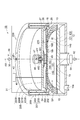
- FIG. 3 is a diagram schematically illustrating a plasma processing apparatus according to an exemplary embodiment.
- FIG. 6 is a perspective view illustrating an upper electrode according to an exemplary embodiment.
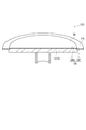
- FIG. 6 is a cutaway perspective view showing a stage according to one exemplary embodiment. It is a figure which shows schematically the plasma processing apparatus which concerns on another exemplary embodiment. It is a figure which shows schematically the plasma processing apparatus which concerns on another example embodiment.
- FIG. 6 is a cutaway perspective view showing a stage according to another exemplary embodiment.
- FIG. 8 is a cutaway perspective view showing a stage according to still another exemplary embodiment.
- a plasma processing apparatus in one exemplary embodiment, includes a processing container, a stage, an upper electrode, and an introduction part.
- the stage is provided in the processing container.
- the upper electrode is provided above the stage via a space inside the processing container.
- the introduction part is a high frequency introduction part which is a VHF wave.
- the introduction portion is provided at a lateral end portion of the space inside the processing container.
- the stage includes a body and a conductive layer.
- the main body is formed of an insulator.
- the conductive layer is provided in the main body.
- the conductive layer has the shortest distance from the top surface of the stage among the one or more conductive layers provided in the stage.
- the conductive layer is any one of an electrode for generating electrostatic attraction between the substrate placed on the stage and the stage, an electrode to which a high frequency is supplied, and an electrode to be grounded.
- the conductive layer is formed in a ring shape.
- the conductive layer is formed in a ring shape, the radial width of the conductive layer is small, and the potential difference generated between the central portion and the outer peripheral portion of the stage is suppressed. It As a result, the high frequency electric field generated between the central portion and the outer peripheral portion of the stage is suppressed.
- the conductive layer may have an outer diameter smaller than the diameter of the substrate mounted on the stage.
- the conductive layer may be formed in a mesh shape.
- the stage may have the conductive layer as a single electrode for generating an electrostatic attractive force between the substrate mounted on the stage and the stage.
- a plasma processing apparatus in another exemplary embodiment, includes a processing container, a stage, an upper electrode, and an introduction part.
- the stage is provided in the processing container and is made of metal.
- the upper electrode is provided above the stage via a space inside the processing container.
- the introduction part is a high frequency introduction part which is a VHF wave.
- the introduction portion is provided at a lateral end portion of the space inside the processing container.
- the upper surface of the stage has a substrate mounting area and a focus ring mounting area.
- the mounting area has a diameter that is smaller than the diameter of the substrate mounted thereon.
- the focus ring mounting region extends radially outside the substrate mounting region.
- the focus ring having an insulating property is mounted on the focus ring mounting area such that the upper surface of the inner edge faces the lower surface of the edge of the substrate mounted on the substrate mounting area. According to this embodiment, the high-frequency electric field generated between the central portion and the outer peripheral portion of the stage is suppressed by the focus ring.
- a plasma processing method for performing plasma processing on a substrate using a plasma processing apparatus includes the step of supplying a gas to the space inside the processing container of the plasma processing apparatus.
- the plasma processing method further includes the step of introducing a high frequency into the space in order to perform the plasma processing on the substrate placed on the stage in the processing container.
- the plasma processing apparatus is any of the plasma processing apparatuses according to the various exemplary embodiments described above.
- the high frequency electric field generated between the central portion and the outer peripheral portion of the stage is suppressed during plasma processing of the substrate.
- FIG. 1 is a diagram schematically showing a plasma processing apparatus according to one exemplary embodiment.
- the plasma processing apparatus 1 shown in FIG. 1 includes a processing container 10, a stage 12, an upper electrode 14, and an introduction section 16.
- the processing container 10 has a substantially cylindrical shape.
- the processing container 10 extends along the vertical direction.
- the central axis of the processing container 10 is an axis AX extending in the vertical direction.
- the processing container 10 is formed of a conductor such as aluminum or an aluminum alloy.
- a film having corrosion resistance is formed on the surface of the processing container 10.
- the film having corrosion resistance may be a yttrium oxide film, a yttrium oxide fluoride film, a yttrium fluoride film, or a ceramic film containing yttrium oxide, yttrium fluoride, or the like.
- the processing container 10 is grounded.
- the stage 12 is provided in the processing container 10.
- the stage 12 is configured to support the substrate W placed on the upper surface thereof substantially horizontally.
- the stage 12 has a substantially disc shape.
- the central axis of the stage 12 may substantially match the axis AX. That is, the center of the stage 12 may be located on the axis AX. Details of the stage 12 will be described later.
- the plasma processing apparatus 1 may further include the baffle member 13.
- the baffle member 13 extends between the stage 12 and the side wall of the processing container 10.
- the baffle member 13 is a substantially annular plate material.
- the baffle member 13 is made of, for example, an insulator such as aluminum oxide.
- a plurality of through holes are formed in the baffle member 13. The plurality of through holes penetrate the baffle member 13 in the plate thickness direction.
- An exhaust port 10e is formed in the processing container 10 below the stage 12.
- An exhaust device is connected to the exhaust port 10e.
- the evacuation device includes a pressure control valve and a vacuum pump such as a turbo molecular pump and/or a dry pump.
- the upper electrode 14 is provided above the stage 12 via the space SP in the processing container 10.
- the upper electrode 14 is formed of a conductor such as aluminum or aluminum alloy.
- the upper electrode 14 has a substantially disc shape.
- the central axis of the upper electrode 14 substantially coincides with the axis AX.
- the plasma processing apparatus 1 is configured to generate plasma in the space SP between the stage 12 and the upper electrode 14. Details of the upper electrode 14 will be described later.
- the plasma processing apparatus 1 may further include the dielectric plate 18.
- the dielectric plate 18 is provided immediately below the upper electrode 14.
- the dielectric plate 18 faces the upper surface of the stage 12 via the space SP.
- the space SP is a space between the dielectric plate 18 and the stage 12.
- the dielectric plate 18 is formed of a dielectric material containing aluminum nitride, aluminum oxide, yttrium oxide, aluminum nitride, aluminum oxide, yttrium oxide, or the like.
- a film having corrosion resistance may be formed on at least the lower surface of the surface of the dielectric plate 18.
- the film having corrosion resistance may be a yttrium oxide film, a yttrium oxide fluoride film, a yttrium fluoride film, or a ceramic film containing yttrium oxide, yttrium fluoride, or the like.
- the dielectric plate 18 has a substantially disc shape. The central axis of the dielectric plate 18 substantially coincides with the axis AX. In one embodiment, the dielectric plate 18 is provided with a plurality of gas discharge holes 18h in order to uniformly supply the gas to the entire surface of the substrate W placed on the stage 12. That is, the dielectric plate 18 may be a shower plate configured to discharge gas.
- the distance in the vertical direction between the lower surface of the dielectric plate 18 and the upper surface of the stage 12 is, for example, 5 cm or more and 30 cm or less.
- the area of the inner wall surface of the processing container 10 extending above the baffle member 13 is substantially equal to the surface area of the dielectric plate 18 on the space SP side. That is, of the surfaces defining the space SP, the area of the surface set to the ground potential (ground surface) is substantially the same as the area of the surface defining the space SP provided by the dielectric plate 18. is there.
- plasma is generated with a uniform density in the region immediately below the dielectric plate and the region around the ground plane. As a result, the in-plane uniformity of the plasma treatment of the substrate W is improved.
- the thickness of the peripheral edge of the dielectric plate 18 is larger than the thickness of the central portion of the dielectric plate 18.
- the central portion of the dielectric plate 18 is a portion that extends inside with respect to the peripheral portion of the dielectric plate 18.
- the peripheral portion of the dielectric plate 18 constitutes the introduction portion 16. That is, the introduction part 16 has a ring shape.
- the introduction unit 16 is a portion that introduces a high frequency into the space SP.
- the high frequency is a VHF wave.
- the introduction part 16 is provided at the lateral end of the space SP.
- the plasma processing apparatus 1 further includes a waveguide section 20 for supplying a high frequency to the introduction section 16.
- the waveguide 20 includes the resonator 200.
- the resonator 200 can be a cavity resonator.
- the resonator 200 provides a waveguide 201.
- the waveguide 201 extends in the direction in which the axis AX extends, and extends in the circumferential direction around the axis AX.
- the waveguide 201 is connected to the introduction unit 16.
- the waveguide 201 has a cylindrical shape extending along the vertical direction.
- the central axis of the waveguide 201 substantially coincides with the axis AX.
- the waveguide 201 includes one end 202 and the other end 203.
- the width of the waveguide 201 between the one end 202 and the other end 203 is set so that the resonator 200 is in a resonance state. That is, the width of the waveguide 201 is set so that the wavelength of the electromagnetic wave propagating in the circumferential direction along the waveguide 201 becomes substantially infinite.
- the width of the waveguide 201 is about 1 ⁇ 2 of the wavelength of the high frequency used (free space wavelength).
- the width of the waveguide 201 can be set to a value obtained by dividing 1/2 of the free space wavelength by the square root of the effective dielectric constant in the waveguide 201. .
- the waveguide 201 includes an inner waveguide 204 and an outer waveguide 205.
- Each of the inner waveguide 204 and the outer waveguide 205 is a tubular waveguide extending along the vertical direction.
- the inner waveguide 204 extends radially inward of the outer waveguide 205.
- the lower end of the outer waveguide 205 constitutes one end 202 of the waveguide 201.
- the upper end of the outer waveguide 205 and the upper end of the inner waveguide 204 are continuous with each other. That is, the waveguide 201 is folded back in the direction in which the axis AX extends.
- the above-mentioned width of the waveguide 201 is the width of the folded waveguide 201 between the one end 202 and the other end 203.
- the lower end of the inner waveguide 204 constitutes the other end 203 of the waveguide 201.
- the other end 203 of the waveguide 201 is connected to the introduction part 16.
- the waveguide unit 20 further includes a first coaxial waveguide 211 and a plurality of second coaxial waveguides 212.
- the first coaxial waveguide 211 extends along the vertical direction so that its central axis line substantially coincides with the axis line AX. That is, the first coaxial waveguide 211 extends on the axis AX.
- the first coaxial waveguide 211 has an inner conductor 213.
- the high frequency power supply 30 is electrically connected to the inner conductor 213 via a matching unit 32.
- the high frequency power supply 30 is a power supply that generates the above-described high frequency.
- the matching device 32 includes a matching circuit for matching the load impedance of the high frequency power supply 30 with the output impedance of the high frequency power supply 30.
- each of the plurality of second coaxial waveguides 212 is connected to the first coaxial waveguide 211.
- Each of the plurality of second coaxial waveguides 212 extends from one end thereof along the radial direction with respect to the axis AX, and is connected to the waveguide 201 of the resonator 200. That is, the plurality of coaxial lines provided by the plurality of second coaxial waveguides 212 are connected to the waveguide 201 of the resonator 200.
- the plurality of second coaxial waveguides 212 are arranged at equal intervals in the circumferential direction with respect to the axis AX, that is, at angular intervals of about 360°/N. Note that “N” is the number of the second coaxial waveguides 212. “N” is, but not limited to, 3 or 4, for example.
- the waveguide 201 of the resonator 200 is provided by the main portion 22 and the cylindrical member 24.
- the main portion 22 is formed of a conductor such as aluminum or aluminum alloy.
- the main portion 22 includes an upper wall portion 221, a central portion 222, and an outer cylindrical portion 223.
- the upper wall portion 221 has a substantially circular shape and a thin plate shape.
- the upper wall portion 221 extends substantially horizontally.
- the central portion 222 has a substantially columnar shape.
- the central portion 222 extends downward from the upper wall portion 221.
- the lower surface of the central portion 222 defines a space 225 inside the peripheral portion of the central portion 222.
- the introduction portion 16, that is, the peripheral edge portion of the dielectric plate 18 is elastically held between the peripheral edge portion of the central portion 222 and the upper end of the processing container 10.
- the sealing member 25 is interposed between the upper end of the processing container 10 and the lower surface of the introduction part 16.
- the sealing member 26 is interposed between the peripheral portion of the central portion 222 and the upper surface of the introduction portion 16.
- Each of the sealing member 25 and the sealing member 26 has elasticity.
- Each of the sealing member 25 and the sealing member 26 extends in the circumferential direction around the axis line AX.
- Each of the sealing member 25 and the sealing member 26 is, for example, an O-ring.
- the peripheral portion of the upper electrode 14 is sandwiched between the peripheral portion of the central portion 222 and the introduction portion 16 on the radially inner side of the sealing member 26.
- a conductive elastic member 27, such as a spiral ring, is provided between the peripheral edge of the upper electrode 14 and the peripheral edge of the central portion 222.
- the material of the conductive elastic member 27 is, for example, a metal such as stainless steel, Inconel, nickel, tungsten, tantalum, a copper alloy, or molybdenum.
- the conductive elastic member 27 may be covered with a protective film of nickel, aluminum, stainless steel, gold, or the like. The conductive elastic member 27 stably maintains the electrical connection between the upper electrode 14 and the central portion 222.
- the outer cylindrical portion 223 has a substantially cylindrical shape.
- the central axis of the outer cylindrical portion 223 substantially coincides with the axis AX.
- the outer cylindrical portion 223 extends radially outward from the central portion 222 and extends downward from the upper wall portion 221.
- the lower end of the outer cylindrical portion 223 is connected to the upper end of the processing container 10. Therefore, the main portion 22 is grounded.
- the cylindrical member 24 is made of a conductor such as aluminum or aluminum alloy.
- the cylindrical member 24 has a substantially cylindrical shape.
- the central axis of the cylindrical member 24 substantially coincides with the axis AX.
- the cylindrical member 24 extends in the vertical direction between the central portion 222 and the outer cylindrical portion 223.
- the lower end of the cylindrical member 24 is connected to the upper end of the processing container 10. Therefore, the cylindrical member 24 is grounded.
- the upper end of the cylindrical member 24 is separated from the upper wall portion 221.
- the outer waveguide 205 extends between the outer cylindrical portion 223 and the cylindrical member 24.
- the outer waveguide 205 terminates at the upper end of the processing container 10.
- the outer waveguide 205 and the inner waveguide 204 are connected between the upper end of the cylindrical member 24 and the upper wall portion 221.
- the inner waveguide 204 extends between the cylindrical member 24 and the central portion 222.
- the central portion 222 of the main portion 22 provides the outer conductor 214 of the first coaxial waveguide 211 and the outer conductor 216 of the plurality of second coaxial waveguides 212. Specifically, the central portion 222 is formed with a hole 217 extending along the axis AX. A portion of the central portion 222 that defines the hole 217 is the outer conductor 214. The inner conductor 213 of the first coaxial waveguide 211 extends along the center line of the hole 217, that is, the axis line AX.
- a plurality of holes 218 extending in the radial direction with respect to the axis AX are formed in the central portion 222.
- the plurality of holes 218 are arranged at an angular interval of about 360°/N in the circumferential direction with respect to the axis AX.
- N is the number of the second coaxial waveguides 212.
- a portion of the central portion 222 that defines the plurality of holes 218 is the outer conductor 216. Inside the plurality of holes 218, the plurality of inner conductors 215, that is, the inner conductors of the plurality of second coaxial waveguides 212, respectively extend.
- Each end of the plurality of inner conductors 215 is connected to the upper end of the cylindrical member 24 by a screw 28.
- the screw 28 extends from the outer cylindrical portion 223 to the end of the corresponding inner conductor 215 among the plurality of inner conductors 215, and is screwed to the corresponding inner conductor 215.
- the head of the screw 28 is in contact with the outer cylindrical portion 223.
- the screw 28 is made of an insulating material.
- the screw 28 is made of, for example, polytetrafluoroethylene.
- a plurality of spacers 29 are provided between the cylindrical member 24 and the outer cylindrical portion 223. Each of the plurality of spacers 29 surrounds a corresponding screw 28 between the cylindrical member 24 and the outer cylindrical portion 223.
- Each of the plurality of spacers 29 is formed of an insulator.
- Each of the plurality of spacers 29 is made of, for example, polytetrafluoroethylene.
- the top electrode 14 includes a first portion 141 and a second portion 142.
- the first portion 141 constitutes the central portion of the upper electrode 14.
- the first portion 141 includes an upper wall 143 and a tubular wall 144.
- the upper wall 143 has a substantially disc shape.
- the upper wall 143 extends substantially horizontally.
- the cylindrical wall 144 has a substantially cylindrical shape.
- the tubular wall 144 extends downward from the peripheral portion of the upper wall 143.
- the thickness of the tubular wall 144 is smaller than the thickness of the upper wall 143 and the thickness of the second portion 142.
- the second portion 142 has a substantially annular and plate shape.
- the second portion 142 extends in the radial direction from the lower end of the tubular wall 144.
- the peripheral portion of the second portion 142 is the peripheral portion of the upper electrode 14.
- the lower surface of the upper electrode 14 defines a gap 145 between the lower surface and the dielectric plate 18 and inside the peripheral portion of the upper electrode 14.
- a plurality of first slits 147 and a plurality of second slits 148 are formed on the upper electrode 14.
- the plurality of first slits 147 and the plurality of second slits 148 penetrate the upper electrode 14.
- Each of the plurality of first slits 147 extends in the radial direction from the cylindrical wall 144 to the peripheral edge of the upper electrode 14.
- the plurality of first slits 147 are arranged, for example, at an angular interval of 360°/M in the circumferential direction. Note that “M” is the number of the plurality of first slits 147.
- Each of the plurality of second slits 148 extends in the radial direction from the position between the cylindrical wall 144 and the peripheral edge of the upper electrode 14 to the peripheral edge of the upper electrode 14.
- the plurality of second slits 148 are arranged alternately with the plurality of first slits 147 in the circumferential direction.
- the pipe 40 extends into the space 225 through the waveguide of the waveguide section 20. As described above, all the waveguides provided by the waveguide unit 20 are configured by grounded conductors. Therefore, the gas is suppressed from being excited in the pipe 40.
- the space 225 is connected to the above-mentioned gap 145 via a plurality of first slits 147 and a plurality of second slits 148.
- the gas from the gas supply unit 42 is supplied to the space 225 via the pipe 40.
- the gas supplied to the space 225 is supplied to the gap 145 through the plurality of first slits 147 and the plurality of second slits 148.
- the gas supplied to the gap 145 is discharged into the space SP via the plurality of gas discharge holes 18h of the dielectric plate 18.
- a high frequency is supplied from the high frequency power supply 30 to the introduction section 16 via the waveguide of the waveguide section 20.
- the resonator 200 of the waveguide section 20 provides a waveguide 201 extending in the direction in which the axis AX extends and extending circumferentially around the axis AX.
- the waveguide 201 extends circumferentially. It is connected to the existing introduction part 16.
- the high frequency wave is introduced into the space SP from the introduction section 16 toward the axis AX. Since the resonator 200 provides the waveguide 201 having the above-described width, the in-tube wavelength along the longitudinal direction of the waveguide 201 (the circumferential direction of the axis AX) becomes infinite.
- the introduction part 16 introduces a high frequency into the space SP with a uniform power in the circumferential direction.
- the high frequency wave is introduced into the space SP, the gas is excited in the space SP and plasma is generated from the gas. Therefore, the plasma is generated in the space SP with a uniform density distribution in the circumferential direction.
- the substrate W on the stage 12 is treated with chemical species from the plasma.
- the substrate is placed on the stage 12.
- gas is supplied to the space SP in the processing container 10.
- the gas is supplied to the space SP from the gas supply unit 42.
- a high frequency is introduced into the space SP.
- the high frequency wave is introduced from the waveguide section 20 into the space SP via the introduction section 16.
- the high frequency wave introduced into the space SP excites the gas in the space SP to generate plasma from the gas.
- the substrate is processed by the generated plasma.
- the high-frequency electric field generated between the central portion and the outer peripheral portion of the stage 12 is suppressed during plasma processing of the substrate. It should be noted that this plasma processing method can be similarly executed by using plasma processing apparatuses of various embodiments described later.
- the above-mentioned gap 145 includes a partial space defined by the first portion 141 and a partial space defined by the second portion 142.
- the vertical length of the partial space defined by the first portion 141 is larger than the vertical length of the partial space defined by the second portion 142. Therefore, the radial non-uniformity of the strength of the electric field formed by the high frequency is reduced.
- the cavity 226 is formed in the central portion 222 of the waveguide 20.
- the actuator 46 is housed in the cavity 226.
- a drive shaft 47 extends downward from the actuator 46 along the axis AX through the central portion 222.
- a sealing member 48 such as an O-ring is provided between the drive shaft 47 and the central portion 222.
- the drive shaft 47 is connected to the upper wall 143 of the first portion 141 of the upper electrode 14.
- the actuator 46 generates power for moving the upper wall 143 up and down. When the upper wall 143 is moved upward by the actuator 46, the length of the gap 145 in the vertical direction increases according to the length of the distance from the axis AX.
- the length of the gap 145 in the vertical direction can be adjusted according to the distance from the axis AX. Therefore, the non-uniformity in the radial direction of the strength of the electric field formed by the high frequency can be eliminated.
- the thickness of the cylindrical wall 144 of the upper electrode 14 is thin. Therefore, the upper electrode 14 is easily bent. Further, the plurality of first slits 147 and the plurality of second slits 148 described above are formed in the upper electrode 14. Therefore, the upper electrode 14 is more easily bent.
- the conductive layer 122 is formed of a conductive material such as tungsten or molybdenum.
- the conductive layer 122 is provided inside the main body 121.
- the stage 12 may have one or more conductive layers. In this case, the conductive layer 122 has the shortest distance from the upper surface of the stage 12 among the one or more conductive layers provided in the stage 12.
- the conductive layer 122 is formed in an annular shape around the axis AX.
- the inner diameter (diameter) of the conductive layer 122 is, for example, 1/6 of the diameter of the substrate W, that is, 50 mm or more.
- the outer diameter of the conductive layer 122 is smaller than the diameter of the substrate W.
- the conductive layer 122 may be formed in a mesh shape.
- the conductive layer 122 is an electrode for electrostatic attraction.
- the DC power supply 50 is electrically connected to the conductive layer 122.
- an electrostatic attractive force is generated between the stage 12 and the substrate W.
- the substrate W is attracted to and held by the stage 12 by the generated electrostatic attraction.
- the conductive layer 122 may be a high frequency electrode.
- a high frequency power source is electrically connected to the conductive layer 122 via a matching unit.
- the conductive layer 122 may be a grounded electrode.
- the conductive layer 122 is formed in a ring shape. Therefore, generation of a potential difference due to high frequency between the central portion and the outer peripheral portion of the stage 12 is suppressed. As a result, the high frequency electric field generated between the central portion and the outer peripheral portion of the stage 12 is suppressed.
- the plasma processing apparatus 1B includes a dielectric plate 18B instead of the dielectric plate 18.
- the dielectric plate 18B is made of a dielectric material containing aluminum nitride, aluminum oxide, yttrium oxide, aluminum nitride, aluminum oxide, yttrium oxide, or the like.
- a film having corrosion resistance may be formed on at least the lower surface of the surface of the dielectric plate 18B.
- the film having corrosion resistance may be a yttrium oxide film, a yttrium oxide fluoride film, a yttrium fluoride film, or a ceramic film containing yttrium oxide, yttrium fluoride, or the like.
- the dielectric plate 18B is formed with a plurality of gas discharge holes 18h, similar to the dielectric plate 18. That is, the dielectric plate 18B may be a shower plate configured to discharge gas.
- the dielectric plate 18B has a substantially disc shape.
- the area of the inner wall surface of the processing container 10 extending above the baffle member 13 is substantially equal to the surface area of the dielectric plate 18B on the space SP side. That is, of the surfaces defining the space SP, the area of the surface (ground surface) set to the ground potential is substantially the same as the area of the surface defining the space SP provided by the dielectric plate 18B. is there.
- the introduction part 16 is separate from the dielectric plate 18B.
- the introduction part 16 is a ring-shaped member.
- the introduction part 16 is formed of a dielectric material such as aluminum nitride or aluminum oxide.
- the waveguide section 20B constitutes the resonator 200.
- the inner waveguide 204 of the resonator 200 extends between the inner cylindrical portion 224B and the cylindrical member 24.
- the outer waveguide 205 of the resonator 200 extends between the outer cylindrical portion 223B and the cylindrical member 24.
- the outer waveguide 205 and the inner waveguide 204 are connected via a gap between the upper end of the cylindrical member 24 and the upper wall portion 221B.
- the inner waveguide 204 is connected to the introduction part 16.
- the introduction portion 16 is sandwiched between the peripheral edge of the central portion 222B and the upper end of the processing container 10 via the sealing member 25 and the sealing member 26.
- the central portion 222B has a substantially disc shape.
- the central portion 222B extends radially inward from the lower end of the inner cylindrical portion 224B.
- the high frequency power supply 30 is electrically connected to the cylindrical member 24.
- the high frequency power supply 30 is electrically connected to the upper portion of the cylindrical member 24 via the coaxial cable 31.
- a variable capacitor 56 is connected between the cylindrical member 24 and the main portion 22B. The capacitance of the variable capacitor 56 is adjusted so as to cause high frequency resonance in the resonator 200. Since the variable capacitor 56 is used in the plasma processing apparatus 1B, the high frequency power supply 30 may be electrically connected to the cylindrical member 24 without a matching device.
- the plasma processing apparatus 1B may further include a dielectric member 49.
- the dielectric member 49 is provided in the space so as to fill the space surrounded by the upper wall 143 and the cylindrical wall 144 of the first portion 141 of the upper electrode 14.
- the dielectric member 49 suppresses electric discharge from occurring in the space.
- the drive shaft 47 has a flange 47f.
- the flange 47f is provided between the upper end and the lower end of the drive shaft 47.
- a bellows 481 is provided between the flange 47f and the central portion 222B. Bellows 481 may be formed of, for example, aluminum, aluminum alloy, or stainless steel.
- a sealing member 482 such as an O-ring is provided between the bellows 481 and the central portion 222B.
- the conductive layer 122 of the stage 12 is a high frequency electrode.
- a high frequency power supply 52 is electrically connected to the conductive layer 122 via a matching unit 54.
- the matching device 54 includes a matching circuit for matching the load impedance of the high frequency power supply 52 with the output impedance of the high frequency power supply 52.
- FIG. 5 is a diagram schematically showing a plasma processing apparatus according to still another exemplary embodiment.
- the configuration of the plasma processing apparatus 1C different from the configuration of the plasma processing apparatus 1 will be described.
- the plasma processing apparatus 1C includes an upper electrode 14C instead of the upper electrode 14.
- the upper electrode 14C has a substantially disc shape.
- the lower surface of the upper electrode 14C includes a region 14r inside the peripheral portion of the upper electrode 14C.
- the vertical position of the region 14r decreases as the distance from the axis AX increases.
- the region 14r is, for example, a concave surface and a curved surface.
- the upper electrode 14C has a protrusion 14p.
- the protrusion 14p has, for example, a rod shape.
- the protrusion 14p extends downward from the center of the region 14r along the axis AX.
- a cavity 14a is provided above the protrusion 14p and inside the upper electrode 14C. Therefore, the portion of the upper electrode 14C between the region 14r and the cavity 14a is thin and easily bends.
- a hole 14b is formed in the upper electrode 14C. The hole 14b connects the cavity 14a and a waveguide 206 (that is, atmospheric pressure space) described later.
- the plasma processing apparatus 1C includes a dielectric plate 18C instead of the dielectric plate 18.
- the dielectric plate 18C has a main body 181 and a conductive film 182.
- the main body 181 is formed of aluminum nitride, aluminum oxide, yttrium oxide, or a dielectric material containing aluminum nitride, aluminum oxide, yttrium oxide, or the like.
- a film having corrosion resistance may be formed on at least the lower surface of the surface of the dielectric plate 18C.
- the film having corrosion resistance may be a yttrium oxide film, a yttrium oxide fluoride film, a yttrium fluoride film, or a ceramic film containing yttrium oxide, yttrium fluoride, or the like.
- the main body 181 has a substantially disc shape.
- the central axis of the main body 181 is substantially coincident with the axis AX.
- the conductive film 182 is formed on the upper surface of the main body 181.
- the conductive film 182 is formed of a material having conductivity.
- the conductive film 182 is formed of, for example, aluminum, nickel, stainless steel, tungsten, molybdenum, copper, or gold.
- the conductive film 182 is, for example, a metal sprayed film.
- the lower end of the protruding portion 14p of the upper electrode 14C is in contact with the conductive film 182.
- the peripheral edge of the dielectric plate 18C is provided between the peripheral edge of the upper electrode 14C and the upper end of the processing container 10.
- a conductive elastic member 271 is provided between the peripheral edge of the dielectric plate 18C and the peripheral edge of the upper electrode 14C.
- the conductive elastic member 271 is, for example, a spiral ring.
- the material of the conductive elastic member 271 is, for example, a metal such as stainless steel, Inconel, nickel, tungsten, tantalum, a copper alloy, or molybdenum.
- the conductive elastic member 271 may be covered with a protective film such as nickel, aluminum, stainless steel, or gold. The conductive elastic member 271 stably maintains the electrical connection between the upper electrode 14C and the conductive film 182.
- the area of the inner wall surface of the processing container 10 extending above the baffle member 13 is substantially equal to the surface area of the dielectric plate 18C on the space SP side. That is, of the surfaces defining the space SP, the area of the surface set to the ground potential (ground surface) is substantially the same as the area of the surface defining the space SP provided by the dielectric plate 18C. is there.
- the peripheral edge of the dielectric plate 18C is sandwiched between the peripheral edge of the upper electrode 14C and the upper end of the processing container 10 via a conductive elastic member 271 and an elastic member 272.
- the elastic member 272 is, for example, an O-ring.
- a support ring 17 may be provided between the peripheral edge of the dielectric plate 18C and the upper end of the processing container 10.
- the support ring 17 is made of a dielectric material such as aluminum nitride or aluminum oxide.
- the elastic member 272 may be interposed between the support ring 17 and the upper end of the processing container 10.
- the introduction part 16 is separate from the dielectric plate 18C.
- the introduction part 16 is a ring-shaped member.
- the introduction part 16 is formed of a dielectric material such as aluminum nitride or aluminum oxide.
- the introduction portion 16 extends in the circumferential direction outside the peripheral edge of the dielectric plate 18C and the support ring 17.
- the introduction portion 16 is sandwiched between the peripheral portion of the upper electrode 14C and the upper end of the processing container 10 via the sealing member 25 and the sealing member 26.
- the dielectric plate 18C has a thickness distribution.
- the dielectric plate 18C has a thickness that decreases as the distance from the axis AX increases.
- the lower surface of the dielectric plate 18C is substantially flat.
- the upper surface of the dielectric plate 18C includes a region 18r that extends inside with respect to the peripheral portion of the dielectric plate 18C. The vertical position of the region 18r becomes lower as the distance from the axis AX increases.
- the region 18r is, for example, a convex surface and a curved surface. Since the dielectric plate 18C has such a thickness distribution, in the plasma processing apparatus 1C, the non-uniformity in the radial direction of the intensity of the electric field formed by the high frequency is reduced.
- the dielectric plate 18C is formed with a plurality of gas discharge holes 18h similarly to the dielectric plate 18. That is, the dielectric plate 18C may be a shower plate configured to discharge gas.
- the plurality of gas discharge holes 18h penetrate the dielectric plate 18C from the region 18r to the lower surface of the dielectric plate 18C.
- Each of the plurality of gas discharge holes 18h includes a small diameter portion and a large diameter portion. In each of the plurality of gas discharge holes 18h, the small-diameter portion extends below the large-diameter portion and is continuous with the large-diameter portion. The lengths of the small-diameter portions of the plurality of gas discharge holes 18h are substantially the same.
- the lengths of the large-diameter portions of the plurality of gas discharge holes 18h are adjusted so that the conductances (gas flow conductances) of the plurality of gas discharge holes 18h are substantially equal to each other.
- the plurality of gas discharge holes 18h have large-diameter portions whose lengths are adjusted according to the thickness of the dielectric plate 18C where they are formed.
- the region 18r of the dielectric plate 18C faces the region 14r of the upper electrode 14C.
- the region 18r and the region 14r are separated from each other.
- a space 14d is provided between the region 18r and the region 14r.
- a pipe 40 is connected to the space 14d.
- a gas supply unit 42 is connected to the pipe 40.
- the gas from the gas supply unit 42 is supplied to the space 14d via the pipe 40.
- the gas supplied to the space 14d is discharged into the space SP through the plurality of gas discharge holes 18h.
- the pressure in the space 14d is lower than atmospheric pressure. Therefore, the protrusion 14p of the upper electrode 14C is biased against the conductive film 182. Therefore, a heat radiation path from the dielectric plate 18C to the upper electrode 14C is stably secured.
- the plasma processing apparatus 1C has a waveguide section 20C instead of the waveguide section 20.
- 20 C of waveguide parts are comprised from 22 C of cylindrical members, and 14 C of upper electrodes.
- the cylindrical member 22C includes an upper wall portion 221C and a cylindrical portion 223C.
- the upper wall portion 221C has a substantially disc shape, and extends horizontally above the upper electrode 14C.
- the upper wall portion 221C is separated from the upper surface of the upper electrode 14C.
- the cylindrical portion 223C has a substantially cylindrical shape.
- the central axis of the cylindrical portion 223C substantially coincides with the axis AX.
- the cylindrical portion 223C extends downward from the peripheral portion of the upper wall portion 221C.
- the lower end of the cylindrical portion 223C is connected to the upper end of the processing container 10. Therefore, the cylindrical member 22C is grounded.
- the cylindrical portion 223C is provided outside the upper electrode 14C in the radial direction so as to surround the upper electrode 14C.
- the cylindrical portion 223C is separated from the upper electrode 14C.
- the waveguide 20C provides a waveguide 206 between the upper wall 221C and the upper surface of the upper electrode 14C.
- the waveguide section 20C provides a cylindrical waveguide 207 between the cylindrical section 223C and the outer peripheral surface of the upper electrode 14C.
- the waveguide 206 is connected to the upper end of the waveguide 207.
- the lower end of the waveguide 207 is connected to the introduction part 16.
- the high frequency power supply 30 is electrically connected to the upper electrode 14C via the matching unit 32.
- the high frequency power from the high frequency power source 30 is supplied to the introduction unit 16 via the waveguide 206 and the waveguide 207.
- the high frequency is supplied to the space SP via the introduction unit 16.
- the high frequency is supplied to the space SP, the gas in the space SP is excited and plasma is formed from the gas.
- the substrate W is treated with chemical species from the plasma.
- the pipe 40 extends to the space 14d through the waveguide 206.
- the upper electrode 14C that defines the waveguide 206 is not grounded.
- the pipe 40 is surrounded by the member 401 in the waveguide 206.
- the member 401 is made of an insulating material. Further, in order to increase the length of the member 401, the upper wall portion 221C is formed so as to project upward around the member 401.
- the plasma processing apparatus 1C includes a stage 12C instead of the stage 12.
- FIG. 6 will be referred to together with FIG.
- FIG. 6 is a cutaway perspective view showing a stage according to another exemplary embodiment.
- the stage 12C has a main body 121 and a conductive layer 122 similarly to the stage 12.
- the conductive layer 122 of the stage 12C is an electrode for electrostatic attraction.
- the DC power supply 50 is electrically connected to the conductive layer 122.
- the stage 12C further includes a conductive layer 123.
- the distance between the conductive layer 123 and the upper surface of the stage 12C is larger than the distance between the conductive layer 122 and the upper surface of the stage 12C. That is, the conductive layer 122 has the shortest distance from the upper surface of the stage 12C among the plurality of conductive layers of the stage 12C.
- the conductive layer 123 is a heater (resistive heating element). In this embodiment, the conductive layer 123 is electrically connected to the heater power supply 58 via the common mode filter 59.
- the conductive layer 123 is formed in an annular region inside the main body 121. The central axis of this annular region substantially coincides with the axis AX.
- the inner diameter of this annular region is, for example, 1/6 of the diameter of the substrate W, that is, 50 mm or more.
- the outer diameter of this annular region is smaller than the diameter of the substrate W.
- the conductive layer 123 may be formed in a mesh shape.
- FIG. 7 is a cutaway perspective view showing a stage according to yet another exemplary embodiment.
- the stage 12D shown in FIG. 7 can be used as a stage of the plasma processing apparatus 1, the plasma processing apparatus 1B, and the plasma processing apparatus 1C.
- the stage 12D has a main body 121D.
- the main body 121D is formed of a metal such as aluminum or an aluminum alloy.
- the main body 121D has a substantially disc shape.
- the central axis line of the main body 121D substantially coincides with the axis line AX.
- the upper surface 12t of the main body 121D includes a substrate mounting area 12w and a focus ring mounting area 12f.
- the substrate mounting area 12w is a substantially circular area.
- the substrate W is placed on the substrate placement area 12w.
- the diameter of the substrate mounting area 12w is smaller than the diameter of the substrate W.
- the focus ring mounting area 12f extends radially and circumferentially outside the substrate mounting area 12w.
- the vertical position of the focus ring mounting area 12f is lower than the vertical position of the substrate mounting area 12w.
- the focus ring FR is mounted on the focus ring mounting area 12f.
- the focus ring FR has a substantially ring shape and a plate shape.
- the focus ring FR is made of aluminum oxide or quartz.
- the focus ring FR is mounted on the focus ring mounting area 12f so that the upper surface of the inner edge thereof faces the lower surface of the edge of the substrate W.
- the focus ring FR suppresses the generation of the high frequency electric field between the central portion and the outer peripheral portion of the stage 12D.
- Plasma processing device 10... Processing container, 12... Stage, 14... Upper electrode, 16... Introduction part, 121... Main body, 122... Conductive layer.
Landscapes
- Physics & Mathematics (AREA)
- Engineering & Computer Science (AREA)
- Plasma & Fusion (AREA)
- Electromagnetism (AREA)
- Spectroscopy & Molecular Physics (AREA)
- Plasma Technology (AREA)
- Drying Of Semiconductors (AREA)
- Container, Conveyance, Adherence, Positioning, Of Wafer (AREA)
Abstract
一つの例示的実施形態に係るプラズマ処理装置は、処理容器、ステージ、上部電極、及び導入部を備える。ステージは、処理容器内に設けられている。上部電極は、ステージの上方に処理容器内の空間を介して設けられている。導入部は、VHF波である高周波の導入部であり、処理容器内の空間の横方向端部に設けられている。ステージは、本体及び導電層を含む。本体は、絶縁体から形成されている。導電層は、本体内に設けられている。導電層は、ステージ内に設けられた一つ以上の導電層のうちステージの上面から最短の距離を有する。導電層は、環状に形成されている。
Description
本開示の例示的実施形態は、プラズマ処理装置及びプラズマ処理方法に関するものである。
電子デバイスの製造においてはプラズマ処理装置が用いられている。一種のプラズマ処理装置は、特許文献1に記載されている。プラズマ処理装置としては、容量結合型のプラズマ処理装置が知られている。容量結合型のプラズマ処理装置として、超短波(VHF)帯の周波数を有する高周波をプラズマの生成に用いるプラズマ処理装置が注目されている。なお、VHF帯とは、30MHz~300MHz程度の範囲の周波数帯である。
VHF帯の周波数を有する高周波をプラズマの生成に用いるプラズマ処理装置においては、ステージの中央部と外周部との間で高周波電界が発生することがある。このような高周波電界の発生を抑制することが求められている。
一つの例示的実施形態において、プラズマ処理装置が提供される。プラズマ処理装置は、処理容器、ステージ、上部電極、及び導入部を備える。ステージは、処理容器内に設けられている。上部電極は、ステージの上方に処理容器内の空間を介して設けられている。導入部は、VHF波である高周波の導入部である。導入部は、処理容器内の空間の横方向端部に設けられている。ステージは、本体及び導電層を含む。本体は、絶縁体から形成されている。導電層は、本体内に設けられている。導電層は、ステージ内に設けられた一つ以上の導電層のうちステージの上面から最短の距離を有する。導電層は、ステージ上に載置される基板とステージとの間で静電引力を発生させるための電極、高周波が供給される電極、及び接地される電極のうち何れかである。導電層は、環状に形成されている。
一つの例示的実施形態に係るプラズマ処理装置によれば、ステージの中央部と外周部との間の高周波電界を抑制することが可能となる。
以下、種々の例示的実施形態について説明する。
一つの例示的実施形態において、プラズマ処理装置が提供される。プラズマ処理装置は、処理容器、ステージ、上部電極、及び導入部を備える。ステージは、処理容器内に設けられている。上部電極は、ステージの上方に処理容器内の空間を介して設けられている。導入部は、VHF波である高周波の導入部である。導入部は、処理容器内の空間の横方向端部に設けられている。ステージは、本体及び導電層を含む。本体は、絶縁体から形成されている。導電層は、本体内に設けられている。導電層は、ステージ内に設けられた一つ以上の導電層のうちステージの上面から最短の距離を有する。導電層は、ステージ上に載置される基板とステージとの間で静電引力を発生させるための電極、高周波が供給される電極、及び接地される電極のうち何れかである。導電層は、環状に形成されている。
上記例示的実施形態に係るプラズマ処理装置では、導電層が環状に形成されているので、導電層の径方向の幅が小さく、ステージの中央部と外周部との間に発生する電位差が抑制される。その結果、ステージの中央部と外周部との間で発生する高周波電界が抑制される。
一つの例示的実施形態において、導電層は、前記ステージ上に載置される基板の直径よりも小さい外径を有していてもよい。
一つの例示的実施形態において、導電層は、メッシュ状に形成されていてもよい。
一つの例示的実施形態において、ステージは、ステージ上に載置される基板とステージとの間で静電引力を発生させるための単一の電極として、前記導電層を有していてもよい。
別の一つの例示的実施形態において、プラズマ処理装置が提供される。プラズマ処理装置は、処理容器、ステージ、上部電極、及び導入部を備える。ステージは、処理容器内に設けられており、金属から形成されている。上部電極は、ステージの上方に処理容器内の空間を介して設けられている。導入部は、VHF波である高周波の導入部である。導入部は、処理容器内の空間の横方向端部に設けられている。ステージの上面は、基板載置領域及びフォーカスリング搭載領域を有する。載置領域は、その上に載置される基板の直径よりも小さい直径を有する。フォーカスリング搭載領域は、基板載置領域よりも径方向外側で延在している。絶縁性を有するフォーカスリングが、その内縁の上面が基板載置領域上に搭載される基板のエッジの下面に対面するように、フォーカスリング搭載領域上に搭載される。この実施形態によれば、フォーカスリングによってステージの中央部と外周部との間で発生する高周波電界が抑制される。
別の例示的実施形態においては、プラズマ処理装置を用いて基板にプラズマ処理を行うプラズマ処理方法が提供される。プラズマ処理方法は、プラズマ処理装置の処理容器内の空間にガスを供給する工程を含む。プラズマ処理方法は、処理容器内でステージ上に載置された基板に対してプラズマ処理を行うために、空間に高周波を導入する工程を更に含む。プラズマ処理装置は、上述した種々の例示的実施形態に係るプラズマ処理装置のうち何れかである。
上記例示的実施形態に係るプラズマ処理方法では、基板に対するプラズマ処理時に、ステージの中央部と外周部との間で発生する高周波電界が抑制される。
以下、図面を参照して種々の例示的実施形態について詳細に説明する。なお、各図面において同一又は相当の部分に対しては同一の符号を附すこととする。
図1は、一つの例示的実施形態に係るプラズマ処理装置を概略的に示す図である。図1に示すプラズマ処理装置1は、処理容器10、ステージ12、上部電極14、及び導入部16を備えている。
処理容器10は、略円筒形状を有する。処理容器10は、鉛直方向に沿って延在している。処理容器10の中心軸線は、鉛直方向に延びる軸線AXである。処理容器10は、アルミニウム又はアルミニウム合金といった導体から形成されている。処理容器10の表面上には、耐腐食性を有する膜が形成されている。耐腐食性を有する膜は、酸化イットリウム膜、酸化フッ化イットリウム膜、フッ化イットリウム膜、又は酸化イットリウム、フッ化イットリウム等を含むセラミック膜であり得る。処理容器10は、接地されている。
ステージ12は、処理容器10内に設けられている。ステージ12は、その上面の上に載置された基板Wを略水平に支持するように構成されている。ステージ12は、略円盤形状を有している。ステージ12の中心軸線は、軸線AXに略一致していてもよい。即ち、ステージ12の中心は、軸線AX上に位置していてもよい。ステージ12の詳細については後述する。
一実施形態において、プラズマ処理装置1は、バッフル部材13を更に備えていてもよい。バッフル部材13は、ステージ12と処理容器10の側壁との間で延在している。バッフル部材13は、略環状の板材である。バッフル部材13は、例えば、酸化アルミニウムといった絶縁体から形成されている。バッフル部材13には、複数の貫通孔が形成されている。複数の貫通孔は、バッフル部材13をその板厚方向に貫通している。ステージ12の下方において処理容器10には、排気口10eが形成されている。排気口10eには、排気装置が接続されている。排気装置は、圧力制御弁並びにターボ分子ポンプ及び/又はドライポンプといった真空ポンプを含んでいる。
上部電極14は、処理容器10内の空間SPを介してステージ12の上方に設けられている。上部電極14は、アルミニウム又はアルミニウム合金といった導体から形成されている。一実施形態において、上部電極14は、略円盤形状を有している。上部電極14の中心軸線は、軸線AXに略一致している。プラズマ処理装置1は、ステージ12と上部電極14との間の空間SPにおいてプラズマを生成するように構成されている。上部電極14の詳細については後述する。
一実施形態において、プラズマ処理装置1は、誘電体板18を更に備えていてもよい。誘電体板18は、上部電極14の直下に設けられている。誘電体板18は、空間SPを介してステージ12の上面に対面している。空間SPは、誘電体板18とステージ12との間の空間である。誘電体板18は、窒化アルミニウム、酸化アルミニウム、酸化イットリウム、又は窒化アルミニウム、酸化アルミニウム、酸化イットリウム等を含む誘電体から形成されている。誘電体板18の表面のうち少なくとも下面には、耐腐食性を有する膜が形成されていてもよい。耐腐食性を有する膜は、酸化イットリウム膜、酸化フッ化イットリウム膜、フッ化イットリウム膜、又は酸化イットリウム、フッ化イットリウム等を含むセラミック膜であり得る。誘電体板18は、略円盤形状を有している。誘電体板18の中心軸線は、軸線AXに略一致している。一実施形態において、誘電体板18には、ステージ12上に載置された基板Wの全面に均等にガスを供給するために、複数のガス吐出孔18hが形成されている。即ち、誘電体板18は、ガスを吐出するように構成されたシャワープレートであってもよい。誘電体板18の下面とステージ12の上面との間の鉛直方向における距離は、例えば5cm以上、30cm以下である。
プラズマ処理装置1では、バッフル部材13の上側で延在する処理容器10の内壁面の面積は、空間SP側の誘電体板18の表面積に略等しい。即ち、空間SPを画成する面のうちグランド電位に設定された面(グランド面)の面積は、空間SPを画成する面のうち誘電体板18によって提供される面の面積と略同一である。かかる構成により、プラズマが、誘電体板の直下の領域及びグランド面の周囲の領域で均一な密度で生成される。その結果、基板Wのプラズマ処理の面内均一性が向上される。
誘電体板18の周縁部の厚みは、誘電体板18の中央部分の厚みよりも大きい。誘電体板18の中央部分は、誘電体板18の周縁部に対して内側で延在する部分である。誘電体板18の周縁部は、導入部16を構成している。即ち、導入部16は、環形状を有している。導入部16は、高周波を空間SPに導入する部分である。高周波は、VHF波である。導入部16は、空間SPの横方向端部に設けられている。プラズマ処理装置1は、導入部16に高周波を供給するために、導波部20を更に備えている。
一実施形態において、導波部20は、共振器200を含んでいる。一実施形態において、共振器200は、空洞共振器であり得る。共振器200は、導波路201を提供している。導波路201は、軸線AXが延在する方向に延び、軸線AXの周りで周方向に延びている。導波路201は、導入部16に接続されている。導波路201は、鉛直方向に沿って延びる筒形状を有している。導波路201の中心軸線は、軸線AXに略一致している。
導波路201は、一端202及び他端203を含んでいる。一端202と他端203との間の導波路201の幅は、共振器200が共振状態となるように設定される。即ち、導波路201の当該幅は、導波路201に沿って周方向に伝搬する電磁波の波長が略無限大になるように設定される。本実施形態においては導波路201の内部が中空であるので、導波路201の幅は、使用される高周波の波長(自由空間波長)の約1/2である。導波路201の内部に誘電体が設けられている場合には、導波路201の幅は、自由空間波長の1/2を導波路201内の実効誘電率の平方根で割った値に設定され得る。
一実施形態において、導波路201は、内側導波路204及び外側導波路205を含んでいる。内側導波路204及び外側導波路205の各々は、鉛直方向に沿って延びる筒状の導波路である。内側導波路204は、外側導波路205に対して径方向内側で延在している。外側導波路205の下端は、導波路201の一端202を構成している。外側導波路205の上端及び内側導波路204の上端は互いに連続している。即ち、導波路201は、軸線AXが延在する方向において折り返されている。なお、導波路201の上述の幅は、一端202と他端203との間の折り返された導波路201の幅である。内側導波路204の下端は、導波路201の他端203を構成している。導波路201の他端203は、導入部16に接続されている。
一実施形態において、導波部20は、第1の同軸導波管211及び複数の第2の同軸導波管212を更に含んでいる。第1の同軸導波管211は、その中心軸線が軸線AXに略一致するように、鉛直方向に沿って延在している。即ち、第1の同軸導波管211は、軸線AX上で延在している。第1の同軸導波管211は、内側導体213を有する。内側導体213には、高周波電源30が、整合器32を介して電気的に接続されている。高周波電源30は、上述した高周波を発生する電源である。整合器32は、高周波電源30の負荷のインピーダンスを高周波電源30の出力インピーダンスに整合させるための整合回路を含んでいる。
複数の第2の同軸導波管212の各々の一端は、第1の同軸導波管211に接続されている。複数の第2の同軸導波管212の各々は、その一端から軸線AXに対して径方向に沿って延在しており、共振器200の導波路201に接続されている。即ち、複数の第2の同軸導波管212によって提供される複数の同軸線路が、共振器200の導波路201に接続されている。複数の第2の同軸導波管212は、軸線AXに対して周方向において、等間隔に、即ち約360°/Nの角度間隔で配列されている。なお、「N」は、第2の同軸導波管212の個数である。「N」は、限定されるものではないが、例えば3又は4である。
一実施形態において、共振器200の導波路201は、主部22及び円筒部材24によって提供されている。主部22は、アルミニウム又はアルミニウム合金といった導体から形成されている。主部22は、上壁部221、中央部222、及び外側円筒部223を含んでいる。上壁部221は、略円形且つ薄板状をなしている。上壁部221は、略水平に延在している。中央部222は、略円柱形状を有している。中央部222は、上壁部221から下方に延びている。中央部222の下面は、中央部222の周縁部の内側に、空間225を画成している。
導入部16、即ち誘電体板18の周縁部は、中央部222の周縁部と処理容器10の上端との間で弾性的に保持されている。具体的に、処理容器10の上端と導入部16の下面との間には、封止部材25が介在している。中央部222の周縁部と導入部16の上面との間には、封止部材26が介在している。封止部材25及び封止部材26の各々は、弾性を有する。封止部材25及び封止部材26の各々は、軸線AXの周りで周方向に延在している。封止部材25及び封止部材26の各々は、例えばOリングである。
上部電極14の周縁部は、封止部材26に対して径方向内側において、中央部222の周縁部と導入部16との間で挟持されている。上部電極14の周縁部と中央部222の周縁部との間には、導電性弾性部材27、例えばスパイラルリングが設けられている。導電性弾性部材27の材料は、例えば、ステンレス鋼、インコネル、ニッケル、タングステン、タンタル、銅合金又はモリブデン等の金属である。導電性弾性部材27は、ニッケル、アルミニウム、ステンレス、又は金等の保護膜により被覆されていてもよい。導電性弾性部材27は、上部電極14と中央部222との間の電気的接続を安定的に維持する。
外側円筒部223は、略円筒形状を有している。外側円筒部223の中心軸線は、軸線AXに略一致している。外側円筒部223は、中央部222に対して径方向外側で、上壁部221から下方に延びている。外側円筒部223の下端は、処理容器10の上端に接続している。したがって、主部22は、接地されている。
円筒部材24は、アルミニウム又はアルミニウム合金といった導体から形成されている。円筒部材24は、略円筒形状を有している。円筒部材24の中心軸線は、軸線AXに略一致している。円筒部材24は、中央部222と外側円筒部223との間で、鉛直方向に延在している。円筒部材24の下端は、処理容器10の上端に接続している。したがって、円筒部材24は、接地されている。円筒部材24の上端は、上壁部221から離れている。
外側導波路205は、外側円筒部223と円筒部材24との間で延在している。外側導波路205は、処理容器10の上端で終端している。外側導波路205と内側導波路204は、円筒部材24の上端と上壁部221との間で接続している。内側導波路204は、円筒部材24と中央部222との間で延在している。
主部22の中央部222は、第1の同軸導波管211の外側導体214及び複数の第2の同軸導波管212の外側導体216を提供している。具体的に、中央部222には、軸線AXに沿って延在する孔217が形成されている。中央部222において孔217を画成する部分は、外側導体214である。第1の同軸導波管211の内側導体213は、孔217の中心線、即ち軸線AXに沿って延在している。
中央部222には、軸線AXに対して径方向に延びる複数の孔218が形成されている。複数の孔218は、軸線AXに対して周方向において、約360°/Nの角度間隔で配列されている。上述したように、「N」は、第2の同軸導波管212の個数である。中央部222において複数の孔218を画成する部分は、外側導体216である。複数の孔218の中では、複数の内側導体215、即ち複数の第2の同軸導波管212の内側導体がそれぞれ延在している。複数の内側導体215は、内側導体213から分岐して、軸線AXに対して径方向に延びている。複数の内側導体215の各々の端部は、円筒部材24の上端に接続されている。したがって、内側導体213及び複数の内側導体215は接地されている。故に、導波部20が提供する導波路は、接地された導体、即ち接地された導波部20の金属壁によって構成されている。
複数の内側導体215の各々の端部は、ねじ28によって円筒部材24の上端に接続されている。ねじ28は、外側円筒部223から複数の内側導体215のうち対応の内側導体215の端部まで延びて、この対応の内側導体215に螺合されている。ねじ28の頭部は、外側円筒部223に当接している。ねじ28は絶縁体から形成されている。ねじ28は、例えばポリテトラフルオロエチレンから形成されている。円筒部材24と外側円筒部223との間には、複数のスペーサ29が設けられている。複数のスペーサ29の各々は、円筒部材24と外側円筒部223との間で対応のねじ28を囲んでいる。複数のスペーサ29の各々は、絶縁体から形成されている。複数のスペーサ29の各々は、例えばポリテトラフルオロエチレンから形成されている。
以下、図1と共に図2を参照する。図2は、一つの例示的実施形態に係る上部電極を示す斜視図である。一実施形態において、上部電極14は、第1部分141及び第2部分142を含んでいる。第1部分141は、上部電極14の中央部分を構成している。第1部分141は、上壁143及び筒状壁144を含んでいる。上壁143は、略円盤形状を有している。上壁143は、略水平に延在している。筒状壁144は、略円筒形状を有している。筒状壁144は、上壁143の周縁部から下方に延在している。なお、筒状壁144の厚み(径方向における厚み)は、上壁143の厚み及び第2部分142の厚みよりも小さい。
第2部分142は、略環状且つ板状をなしている。第2部分142は、筒状壁144の下端から径方向に延在している。第2部分142の周縁部は、上部電極14の周縁部である。上部電極14の下面は、当該下面と誘電体板18との間、且つ、上部電極14の周縁部の内側に間隙145を画成している。
上部電極14には、複数の第1のスリット147及び複数の第2のスリット148が形成されている。複数の第1のスリット147及び複数の第2のスリット148は、上部電極14を貫通している。複数の第1のスリット147の各々は、筒状壁144から上部電極14の周縁まで、径方向に沿って延びている。複数の第1のスリット147は、例えば、周方向において360°/Mの角度間隔で配列されている。なお、「M」は、複数の第1のスリット147の個数である。
複数の第2のスリット148の各々は、筒状壁144と上部電極14の周縁との間の位置から上部電極14の周縁まで、径方向に沿って延びている。複数の第2のスリット148は、周方向において、複数の第1のスリット147と交互に配列されている。
上述の空間225には、配管40が接続されている。配管40には、ガス供給部42が接続されている。ガス供給部42は、基板Wの処理のために用いられる一つ以上のガス源を含む。また、ガス供給部42は、一つ以上のガス源からのガスの流量をそれぞれ制御するための一つ以上の流量制御器を含む。
配管40は、導波部20の導波路を通って空間225に延びている。上述したように導波部20が提供する全ての導波路は、接地された導体によって構成されている。したがって、配管40内でガスが励起されることが抑制される。
空間225は、上述の間隙145に、複数の第1のスリット147及び複数の第2のスリット148を介して接続されている。ガス供給部42からのガスは、配管40を介して空間225に供給される。空間225に供給されたガスは、複数の第1のスリット147及び複数の第2のスリット148を介して、間隙145に供給される。間隙145に供給されたガスは、誘電体板18の複数のガス吐出孔18hを介して、空間SPに吐出される。
プラズマ処理装置1では、高周波電源30から導波部20の導波路を介して導入部16に高周波が供給される。導波部20の共振器200は、軸線AXが延在する方向に延び、且つ、軸線AXの周りで周方向に延びる導波路201を提供している、この導波路201は、周方向に延在する導入部16に接続されている。高周波は、この導入部16から軸線AXに向けて空間SP内に導入される。共振器200は上述した幅の導波路201を提供しているので、導波路201の長手方向(軸線AXの周方向)に沿った管内波長が無限大となる。その結果、導入部16には周方向に均一な強度及び位相の電界が印加される。したがって、導入部16からは、周方向において均一なパワーで高周波が空間SP内に導入される。高周波が空間SPに導入されると、ガスが空間SP内で励起されて、当該ガスからプラズマが生成される。したがって、プラズマは、空間SP内で周方向において均一な密度分布で生成される。ステージ12上の基板Wは、プラズマからの化学種によって処理される。
以下、プラズマ処理装置1を用いて基板にプラズマ処理を行うプラズマ処理方法について説明する。プラズマ処理方法では、ステージ12上に基板が載置される。次いで、プラズマ処理方法では、処理容器10内の空間SPにガスが供給される。ガスは、ガス供給部42から空間SPに供給される。次いで、プラズマ処理方法では、空間SPに高周波が導入される。高周波は、導波部20から導入部16を介して空間SPに導入される。空間SP内に導入された高周波は、空間SP内でガスを励起させて、当該ガスからプラズマを生成する。生成されたプラズマによって、基板が処理される。このプラズマ処理方法では、基板に対するプラズマ処理時に、ステージ12の中央部と外周部との間で発生する高周波電界が抑制される。なお、このプラズマ処理方法は、後述する種々の実施形態のプラズマ処理装置を用いて同様に実行され得る。
上述した間隙145は、第1部分141によって画成されている部分空間と第2部分142によって画成されている部分空間を含む。第1部分141によって画成されている部分空間の鉛直方向における長さは、第2部分142によって画成されている部分空間の鉛直方向における長さよりも大きい。したがって、高周波によって形成される電界の強度の径方向における不均一性が低減される。
一実施形態において、空洞226が導波部20の中央部222内に形成されている。空洞226の中には、アクチュエータ46が収容されている。アクチュエータ46からは、駆動軸47が、中央部222を貫いて軸線AXに沿って下方に延びている。駆動軸47と中央部222との間には、Oリングといった封止部材48が設けられている。駆動軸47は、上部電極14の第1部分141の上壁143に接続されている。アクチュエータ46は、上壁143を上下に移動させる動力を発生する。アクチュエータ46によって、上壁143が上方に移動されると、間隙145の鉛直方向における長さは、軸線AXからの距離の長さに応じて増加する。即ち、アクチュエータ46によって上壁143の鉛直方向における位置を調整することにより、間隙145の鉛直方向における長さを軸線AXからの距離に応じて調整することができる。したがって、高周波によって形成される電界の強度の径方向における不均一性が解消され得る。
上述したように、上部電極14の筒状壁144の厚みは、薄くなっている。したがって、上部電極14は、撓み易くなっている。さらに、上部電極14には、上述した複数の第1のスリット147及び複数の第2のスリット148が形成されている。したがって、上部電極14は、更に撓み易くなっている。
以下、図1と共に図3を参照する。図3は、一つの例示的実施形態に係るステージを示す破断斜視図である。ステージ12は、本体121及び導電層122を有している。本体121は、窒化アルミニウムといった絶縁体から形成されている。本体121は、略円盤形状を有している。本体121の中心軸線は、軸線AXと略一致している。
導電層122は、導電性を有する材料、例えばタングステン、モリブデン等から形成されている。導電層122は、本体121内に設けられている。ステージ12は、一つ以上の導電層を有していてもよい。この場合に、導電層122は、ステージ12内に設けられた一つ以上の導電層のうちステージ12の上面から最短の距離を有する。
導電層122は、軸線AXの周りで環状に形成されている。導電層122の内径(直径)は、例えば基板Wの直径の1/6、即ち50mm以上である。導電層122の外径は、基板Wの直径よりも小さい。一実施形態において、導電層122は、メッシュ状に形成されていてもよい。
一実施形態において、導電層122は、静電吸着用の電極である。この実施形態において、導電層122には、直流電源50が電気的に接続される。直流電源50からの直流電圧が導電層122に印加されると、ステージ12と基板Wとの間で静電引力が発生する。発生した静電引力により、基板Wは、ステージ12に引き付けられ、ステージ12によって保持される。別の実施形態において、導電層122は、高周波電極であってもよい。この場合には、導電層122には、高周波電源が整合器を介して電気的に接続される。更に別の実施形態において、導電層122は、接地される電極であってもよい。
以上説明したプラズマ処理装置1では、導電層122が環状に形成されている。したがって、ステージ12の中央部と外周部との間での高周波に起因する電位差の発生が抑制される。その結果、ステージ12の中央部と外周部との間で発生する高周波電界が抑制される。
以下、図4を参照して、別の例示的実施形態に係るプラズマ処理装置1Bについて説明する。図4は、別の例示的実施形態に係るプラズマ処理装置を概略的に示す図である。以下、プラズマ処理装置1の構成と異なるプラズマ処理装置1Bの構成について説明する。
プラズマ処理装置1Bは、誘電体板18に代えて、誘電体板18Bを備えている。誘電体板18Bは、窒化アルミニウム、酸化アルミニウム、酸化イットリウム、又は窒化アルミニウム、酸化アルミニウム、酸化イットリウム等を含む誘電体から形成されている。誘電体板18Bの表面のうち少なくとも下面には、耐腐食性を有する膜が形成されていてもよい。耐腐食性を有する膜は、酸化イットリウム膜、酸化フッ化イットリウム膜、フッ化イットリウム膜、又は酸化イットリウム、フッ化イットリウム等を含むセラミック膜であり得る。一実施形態において、誘電体板18Bには、誘電体板18と同様に、複数のガス吐出孔18hが形成されている。即ち、誘電体板18Bは、ガスを吐出するように構成されたシャワープレートであってもよい。誘電体板18Bは、略円盤形状を有する。
プラズマ処理装置1Bにおいても、バッフル部材13の上側で延在する処理容器10の内壁面の面積は、空間SP側の誘電体板18Bの表面積に略等しい。即ち、空間SPを画成する面のうちグランド電位に設定された面(グランド面)の面積は、空間SPを画成する面のうち誘電体板18Bによって提供される面の面積と略同一である。
プラズマ処理装置1Bでは、導入部16は、誘電体板18Bとは別体である。プラズマ処理装置1Bにおいて、導入部16は、リング状の部材である。導入部16は、窒化アルミニウム又は酸化アルミニウムといった誘電体から形成されている。
プラズマ処理装置1Bは、導波部20に代えて、導波部20Bを備えている。導波部20Bは、主部22B及び円筒部材24を有する。主部22Bは、アルミニウム又はアルミニウム合金といった導体から形成されている。主部22Bは、上壁部221B、中央部222B、外側円筒部223B、及び内側円筒部224Bを含んでいる。
上壁部221Bは、略環形状を有しており、板状をなしている。上壁部221Bの中心軸線は、軸線AXに略一致している。外側円筒部223B及び内側円筒部224Bは、略円筒形状を有している。外側円筒部223B及び内側円筒部224Bの各々の中心軸線は、軸線AXに略一致している。内側円筒部224Bは、外側円筒部223Bに対して径方向内側に設けられている。内側円筒部224Bは、上壁部221Bの内縁から下方に延びている。外側円筒部223Bは、上壁部221Bの外縁から下方に延びている。円筒部材24は、外側円筒部223Bと内側円筒部224Bとの間で延在している。円筒部材24の上端は、上壁部221Bから離間している。
導波部20Bは、共振器200を構成している。共振器200の内側導波路204は、内側円筒部224Bと円筒部材24との間で延在している。共振器200の外側導波路205は、外側円筒部223Bと円筒部材24との間で延在している。外側導波路205と内側導波路204は、円筒部材24の上端と上壁部221Bとの間の間隙を介して接続されている。内側導波路204は、導入部16に接続されている。導入部16は、中央部222Bの周縁部と処理容器10の上端との間で、封止部材25及び封止部材26を介して挟持されている。中央部222Bは、略円盤形状を有している。中央部222Bは、内側円筒部224Bの下端から径方向内側に延在している。
プラズマ処理装置1Bでは、高周波電源30は、円筒部材24に電気的に接続されている。一実施形態では、高周波電源30は、同軸ケーブル31を介して円筒部材24の上部に電気的に接続されている。円筒部材24と主部22Bとの間には、可変コンデンサ56が接続されている。可変コンデンサ56の静電容量は、共振器200内で高周波の共振を生じさせるように、調整される。プラズマ処理装置1Bでは、かかる可変コンデンサ56が用いられるので、高周波電源30は、整合器を介することなく、円筒部材24に電気的に接続されてもよい。
プラズマ処理装置1Bは、誘電体部材49を更に備えていてもよい。誘電体部材49は、上部電極14の第1部分141の上壁143及び筒状壁144によって囲まれた空間を埋めるように当該空間内に設けられている。誘電体部材49は、当該空間において放電が生じることを抑制する。
プラズマ処理装置1Bでは、駆動軸47は、フランジ47fを有している。フランジ47fは、駆動軸47の上端と下端との間に設けられている。フランジ47fと中央部222Bとの間には、ベローズ481が設けられている。ベローズ481は、例えばアルミニウム、アルミニウム合金、又はステンレス鋼から形成され得る。ベローズ481と中央部222Bとの間には、Oリングといった封止部材482が設けられている。
プラズマ処理装置1Bでは、ステージ12の導電層122は、高周波電極である。導電層122には、高周波電源52が整合器54を介して電気的に接続されている。整合器54は、高周波電源52の負荷のインピーダンスを高周波電源52の出力インピーダンスに整合させるための整合回路を含んでいる。
以下、図5を参照して、更に別の例示的実施形態に係るプラズマ処理装置1Cについて説明する。図5は、更に別の例示的実施形態に係るプラズマ処理装置を概略的に示す図である。以下、プラズマ処理装置1の構成とは異なるプラズマ処理装置1Cの構成について、説明する。
プラズマ処理装置1Cは、上部電極14に代えて、上部電極14Cを備えている。上部電極14Cは、略円盤形状を有している。上部電極14Cの下面は、上部電極14Cの周縁部の内側に、領域14rを含んでいる。領域14rの鉛直方向の位置は、軸線AXからの距離の増加に応じて低くなっている。領域14rは、例えば凹面であり曲面である。
上部電極14Cは、突出部14pを有する。突出部14pは、例えば棒形状を有している。突出部14pは、領域14rの中心から軸線AXに沿って下方に延びている。突出部14pの上方、且つ、上部電極14C内には、空洞14aが設けられている。したがって、領域14rと空洞14aとの間の上部電極14Cの部位は、薄くなっており、撓み易くなっている。上部電極14Cには、孔14bが形成されている。孔14bは、空洞14aと後述する導波路206(即ち、大気圧空間)とを接続している。
プラズマ処理装置1Cは、誘電体板18に代えて、誘電体板18Cを備えている。誘電体板18Cは、本体181と導電膜182を有している。本体181は、窒化アルミニウム、酸化アルミニウム、酸化イットリウム、又は窒化アルミニウム、酸化アルミニウム、酸化イットリウム等を含む誘電体から形成されている。誘電体板18Cの表面のうち少なくとも下面には、耐腐食性を有する膜が形成されていてもよい。耐腐食性を有する膜は、酸化イットリウム膜、酸化フッ化イットリウム膜、フッ化イットリウム膜、又は酸化イットリウム、フッ化イットリウム等を含むセラミック膜であり得る。本体181は、略円盤形状を有している。本体181の中心軸線は軸線AXに略一致している。導電膜182は、本体181の上面の上に形成されている。導電膜182は、導電性を有する材料から形成されている。導電膜182は、例えば、アルミニウム、ニッケル、ステンレス鋼、タングステン、モリブデン、銅、又は金から形成されている。導電膜182は、例えば金属の溶射膜である。導電膜182には、上部電極14Cの突出部14pの下端が当接している。
誘電体板18Cの周縁部は、上部電極14Cの周縁部と処理容器10の上端との間に設けられている。誘電体板18Cの周縁部と上部電極14Cの周縁部との間には、導電性弾性部材271が設けられている。導電性弾性部材271は、例えばスパイラルリングである。導電性弾性部材271の材料は、例えば、ステンレス鋼、インコネル、ニッケル、タングステン、タンタル、銅合金又はモリブデン等の金属である。導電性弾性部材271は、ニッケル、アルミニウム、ステンレス、又は金等の保護膜により被覆されていてもよい。導電性弾性部材271は、上部電極14Cと導電膜182との間の電気的接続を安定的に維持する。
プラズマ処理装置1Cにおいても、バッフル部材13の上側で延在する処理容器10の内壁面の面積は、空間SP側の誘電体板18Cの表面積に略等しい。即ち、空間SPを画成する面のうちグランド電位に設定された面(グランド面)の面積は、空間SPを画成する面のうち誘電体板18Cによって提供される面の面積と略同一である。
誘電体板18Cの周縁部は、上部電極14Cの周縁部と処理容器10の上端との間で導電性弾性部材271及び弾性部材272を介して挟持されている。弾性部材272は、例えばOリングである。誘電体板18Cの周縁部と処理容器10の上端との間には、サポートリング17が設けられていてもよい。サポートリング17は、窒化アルミニウムまたは酸化アルミニウムといった誘電体から形成されている。弾性部材272は、サポートリング17と処理容器10の上端との間に介在していてもよい。
プラズマ処理装置1Cでは、導入部16は、誘電体板18Cとは別体である。プラズマ処理装置1Cにおいて、導入部16は、リング状の部材である。導入部16は、窒化アルミニウム又は酸化アルミニウムといった誘電体から形成されている。導入部16は、誘電体板18Cの周縁部及びサポートリング17の外側で周方向に延在している。導入部16は、上部電極14Cの周縁部と処理容器10の上端との間で、封止部材25及び封止部材26を介して挟持されている。
誘電体板18Cは厚みの分布を有する。一実施形態において、誘電体板18Cの厚みは、軸線AXからの距離の増加に応じて薄くなっている。誘電体板18Cの下面は、略平坦である。誘電体板18Cの上面は、誘電体板18Cの周縁部に対して内側で延在する領域18rを含んでいる。領域18rの鉛直方向の位置は、軸線AXからの距離の増加に応じて、低くなっている。領域18rは、例えば凸面であり曲面である。誘電体板18Cがかかる厚みの分布を有するので、プラズマ処理装置1Cでは、高周波によって形成される電界の強度の径方向における不均一性が低減される。
一実施形態において、誘電体板18Cには、誘電体板18と同様に複数のガス吐出孔18hが形成されている。即ち、誘電体板18Cは、ガスを吐出するように構成されたシャワープレートであってもよい。複数のガス吐出孔18hは、領域18rから誘電体板18Cの下面まで、誘電体板18Cを貫通している。複数のガス吐出孔18hの各々は、小径の部位と大径の部位を含んでいる。複数のガス吐出孔18hの各々において、小径の部位は、大径の部位の下方で延在しており、大径の部位に連続している。複数のガス吐出孔18hの小径の部位の長さは、互いに略同一である。複数のガス吐出孔18hの大径の部位の長さは、複数のガス吐出孔18hのコンダクタンス(ガスフローコンダクタンス)を互いに略等しくするように、調整されている。具体的には、複数のガス吐出孔18hは、それらが形成されている箇所の誘電体板18Cの厚みの大きさに応じて長さが大きくなるように調整された大径の部位を有する。
誘電体板18Cの領域18rは、上部電極14Cの領域14rに対面している。領域18rと領域14rは、互いに離間している。領域18rと領域14rとの間には、空間14dが設けられている。空間14dには、配管40が接続されている。配管40には、ガス供給部42が接続されている。
ガス供給部42からのガスは、配管40を介して空間14dに供給される。空間14dに供給されたガスは、複数のガス吐出孔18hを介して空間SPに吐出される。空間14d内の圧力は、大気圧よりも低い。したがって、上部電極14Cの突出部14pは導電膜182に対して付勢されている。故に、誘電体板18Cから上部電極14Cへの放熱パスが安定的に確保される。
プラズマ処理装置1Cは、導波部20に代えて、導波部20Cを有している。導波部20Cは、円筒部材22C及び上部電極14Cから構成されている。円筒部材22Cは、上壁部221C及び円筒部223Cを含んでいる。上壁部221Cは、略円盤形状を有しており、上部電極14Cの上方で水平に延在している。上壁部221Cは、上部電極14Cの上面から離間している。円筒部223Cは、略円筒形状を有している。円筒部223Cの中心軸線は、軸線AXと略一致している。円筒部223Cは、上壁部221Cの周縁部から下方に延在している。円筒部223Cの下端は、処理容器10の上端に接続している。したがって、円筒部材22Cは接地されている。円筒部223Cは、上部電極14Cを囲むように、上部電極14Cの径方向外側に設けられている。円筒部223Cは、上部電極14Cから離間している。
導波部20Cは、上壁部221Cと上部電極14Cの上面との間に、導波路206を提供している。導波部20Cは、円筒部223Cと上部電極14Cの外周面との間に、筒状の導波路207を提供している。導波路206は導波路207の上端に接続している。導波路207の下端は、導入部16に接続している。
プラズマ処理装置1Cでは、高周波電源30は、整合器32を介して上部電極14Cに電気的に接続されている。高周波電源30からの高周波は、導波路206及び導波路207を介して導入部16に供給される。高周波は、導入部16を介して空間SPに供給される。高周波が空間SPに供給されると、空間SP内のガスが励起されて、当該ガスからプラズマが形成される。基板Wは、プラズマからの化学種によって処理される。
プラズマ処理装置1Cでは、配管40は導波路206を通って空間14dまで延びている。導波路206を画成する上部電極14Cは、接地されていない。配管40の中でガスが励起されることを防止するために、配管40は、導波路206の中では部材401によって囲まれている。部材401は、絶縁性を有する材料から形成されている。また、部材401の長さを長くするために、上壁部221Cは、部材401の周囲で上方へ突出するように形成されている。
プラズマ処理装置1Cは、ステージ12に代えて、ステージ12Cを備えている。以下、図5と共に図6を参照する。図6は、別の例示的実施形態に係るステージを示す破断斜視図である。ステージ12Cは、ステージ12と同様に本体121及び導電層122を有している。ステージ12Cの導電層122は、静電吸着用の電極である。導電層122には、直流電源50が電気的に接続されている。
ステージ12Cは、導電層123を更に備えている。導電層123とステージ12Cの上面との間の距離は、導電層122とステージ12Cの上面との間の距離よりも大きい。即ち、導電層122は、ステージ12Cの複数の導電層のうち、ステージ12Cの上面から最短の距離を有する。
一実施形態において、導電層123は、ヒータ(抵抗加熱素子)である。この実施形態では、導電層123は、ヒータ電源58にコモンモードフィルタ59を介して電気的に接続されている。導電層123は、本体121内の環状の領域内に形成されている。この環状の領域の中心軸線は、軸線AXに略一致する。この環状の領域の内径は、例えば基板Wの直径の1/6、即ち50mm以上である。この環状の領域の外径は、基板Wの直径よりも小さい。導電層123は、メッシュ状に形成されていてもよい。
以下、図7を参照して、更に別の例示的実施形態に係るステージ12Dについて説明する。図7は、更に別の例示的実施形態に係るステージを示す破断斜視図である。図7に示すステージ12Dは、プラズマ処理装置1、プラズマ処理装置1B、及びプラズマ処理装置1Cのステージとして利用され得る。
ステージ12Dは、本体121Dを有する。本体121Dは、アルミニウム又はアルミニウム合金といった金属から形成されている。本体121Dは、略円盤形状を有する。本体121Dの中心軸線は、軸線AXに略一致している。
本体121Dの上面12tは、基板載置領域12w及びフォーカスリング搭載領域12fを含んでいる。基板載置領域12wは、略円形の領域である。基板Wは、基板載置領域12w上に載置される。基板載置領域12wの直径は、基板Wの直径よりも小さい。フォーカスリング搭載領域12fは、基板載置領域12wの外側で径方向及び周方向に延在している。フォーカスリング搭載領域12fの鉛直方向の位置は、基板載置領域12wの鉛直方向の位置のよりも低い。
フォーカスリング搭載領域12f上には、フォーカスリングFRが搭載される。フォーカスリングFRは、略環形状を有しており、板状をなしている。フォーカスリングFRは、酸化アルミニウム又は石英から形成されている。フォーカスリングFRは、その内縁の上面が基板Wのエッジの下面に面するように、フォーカスリング搭載領域12f上に搭載される。
このステージ12Dによれば、ステージ12Dの中央部と外周部との間での高周波電界の発生がフォーカスリングFRによって抑制される。
以上、種々の例示的実施形態について説明してきたが、上述した例示的実施形態に限定されることなく、様々な省略、置換、及び変更がなされてもよい。また、異なる実施形態における要素を組み合わせて他の実施形態を形成することが可能である。
以上の説明から、本開示の種々の実施形態は、説明の目的で本明細書で説明されており、本開示の範囲及び主旨から逸脱することなく種々の変更をなし得ることが、理解されるであろう。したがって、本明細書に開示した種々の実施形態は限定することを意図しておらず、真の範囲と主旨は、添付の特許請求の範囲によって示される。
1…プラズマ処理装置、10…処理容器、12…ステージ、14…上部電極、16…導入部、121…本体、122…導電層。
Claims (4)
- 処理容器と、
前記処理容器内に設けられたステージと、
前記ステージの上方に前記処理容器内の空間を介して設けられた上部電極と、
VHF波である高周波の導入部であって、前記空間の横方向端部に設けられた、該導入部と、
を備え、
前記ステージは、
絶縁体から形成された本体と、
前記本体内に設けられた導電層と、
を含み、
前記導電層は、前記ステージ内に設けられた一つ以上の導電層のうち前記ステージの上面から最短の距離を有し、前記ステージ上に載置される基板と該ステージとの間で静電引力を発生させるための電極、高周波が供給される電極、及び接地される電極のうち何れかかであり、環状に形成されている、
プラズマ処理装置。 - 前記導電層は、前記ステージ上に載置される基板の直径よりも小さい外径を有する、
請求項1に記載のプラズマ処理装置。 - 前記導電層は、メッシュ状に形成されている、請求項1又は2に記載のプラズマ処理装置。
- プラズマ処理装置を用いて基板にプラズマ処理を行うプラズマ処理方法であって、
前記プラズマ処理装置の処理容器内の空間にガスを供給する工程と、
前記処理容器内でステージ上に載置された基板に対してプラズマ処理を行うために、前記空間に高周波を導入する工程と、
を含み、
前記プラズマ処理装置は、
前記処理容器と、
前記処理容器内に設けられた前記ステージと、
前記ステージの上方に前記処理容器内の前記空間を介して設けられた上部電極と、
VHF波である高周波の導入部であって、前記空間の横方向端部に設けられた、該導入部と、
を備え、
前記ステージは、
絶縁体から形成された本体と、
前記本体内に設けられた導電層と、
を含み、
前記導電層は、前記ステージ内に設けられた一つ以上の導電層のうち前記ステージの上面から最短の距離を有し、前記ステージ上に載置される基板と該ステージとの間で静電引力を発生させるための電極、高周波が供給される電極、及び接地される電極のうち何れかかであり、環状に形成されている、
プラズマ処理方法。
Applications Claiming Priority (2)
| Application Number | Priority Date | Filing Date | Title |
|---|---|---|---|
| JP2018-229244 | 2018-12-06 | ||
| JP2018229244A JP2020092195A (ja) | 2018-12-06 | 2018-12-06 | プラズマ処理装置及びプラズマ処理方法 |
Publications (1)
| Publication Number | Publication Date |
|---|---|
| WO2020116259A1 true WO2020116259A1 (ja) | 2020-06-11 |
Family
ID=70973773
Family Applications (1)
| Application Number | Title | Priority Date | Filing Date |
|---|---|---|---|
| PCT/JP2019/046238 Ceased WO2020116259A1 (ja) | 2018-12-06 | 2019-11-26 | プラズマ処理装置及びプラズマ処理方法 |
Country Status (2)
| Country | Link |
|---|---|
| JP (1) | JP2020092195A (ja) |
| WO (1) | WO2020116259A1 (ja) |
Families Citing this family (1)
| Publication number | Priority date | Publication date | Assignee | Title |
|---|---|---|---|---|
| JP7716347B2 (ja) * | 2022-01-25 | 2025-07-31 | 東京エレクトロン株式会社 | プラズマ処理装置 |
Citations (7)
| Publication number | Priority date | Publication date | Assignee | Title |
|---|---|---|---|---|
| JP2000012292A (ja) * | 1998-06-19 | 2000-01-14 | Sumitomo Metal Ind Ltd | プラズマ処理装置 |
| JP2003077699A (ja) * | 2001-09-04 | 2003-03-14 | Canon Inc | プラズマ処理方法及び装置 |
| JP2008042140A (ja) * | 2006-08-10 | 2008-02-21 | Tokyo Electron Ltd | 静電チャック装置 |
| JP2010232532A (ja) * | 2009-03-27 | 2010-10-14 | Sumitomo Electric Ind Ltd | 高周波電極の接続方法を改善したウエハ保持体及びそれを搭載した半導体製造装置 |
| JP2011165891A (ja) * | 2010-02-09 | 2011-08-25 | Tokyo Electron Ltd | 載置台構造及び処理装置 |
| US20130098873A1 (en) * | 2011-10-20 | 2013-04-25 | Applied Materials, Inc. | Overhead electron beam source for plasma ion generation in a workpiece processing region |
| JP2018510470A (ja) * | 2015-03-17 | 2018-04-12 | アプライド マテリアルズ インコーポレイテッドApplied Materials,Incorporated | イオン−イオンプラズマ原子層エッチングプロセス及びリアクタ |
-
2018
- 2018-12-06 JP JP2018229244A patent/JP2020092195A/ja active Pending
-
2019
- 2019-11-26 WO PCT/JP2019/046238 patent/WO2020116259A1/ja not_active Ceased
Patent Citations (7)
| Publication number | Priority date | Publication date | Assignee | Title |
|---|---|---|---|---|
| JP2000012292A (ja) * | 1998-06-19 | 2000-01-14 | Sumitomo Metal Ind Ltd | プラズマ処理装置 |
| JP2003077699A (ja) * | 2001-09-04 | 2003-03-14 | Canon Inc | プラズマ処理方法及び装置 |
| JP2008042140A (ja) * | 2006-08-10 | 2008-02-21 | Tokyo Electron Ltd | 静電チャック装置 |
| JP2010232532A (ja) * | 2009-03-27 | 2010-10-14 | Sumitomo Electric Ind Ltd | 高周波電極の接続方法を改善したウエハ保持体及びそれを搭載した半導体製造装置 |
| JP2011165891A (ja) * | 2010-02-09 | 2011-08-25 | Tokyo Electron Ltd | 載置台構造及び処理装置 |
| US20130098873A1 (en) * | 2011-10-20 | 2013-04-25 | Applied Materials, Inc. | Overhead electron beam source for plasma ion generation in a workpiece processing region |
| JP2018510470A (ja) * | 2015-03-17 | 2018-04-12 | アプライド マテリアルズ インコーポレイテッドApplied Materials,Incorporated | イオン−イオンプラズマ原子層エッチングプロセス及びリアクタ |
Also Published As
| Publication number | Publication date |
|---|---|
| JP2020092195A (ja) | 2020-06-11 |
Similar Documents
| Publication | Publication Date | Title |
|---|---|---|
| US12488964B2 (en) | Plasma processing apparatus and plasma processing method | |
| KR101124811B1 (ko) | 플라즈마 처리 장치 | |
| US11923170B2 (en) | Plasma processing apparatus and plasma processing method | |
| JP2015162266A (ja) | プラズマ処理装置 | |
| US11854772B2 (en) | Plasma processing apparatus and plasma processing method | |
| JPWO2020116246A1 (ja) | シャワープレート、プラズマ処理装置及びプラズマ処理方法 | |
| US20160372306A1 (en) | Method for Controlling Plasma Uniformity in Plasma Processing Systems | |
| JP6785377B2 (ja) | プラズマ処理装置 | |
| TW202441572A (zh) | 具有阻抗匹配射頻(rf)桿的加熱基座 | |
| KR102229990B1 (ko) | 플라즈마 처리 장치용 부재 및 플라즈마 처리 장치 | |
| WO2020116259A1 (ja) | プラズマ処理装置及びプラズマ処理方法 | |
| WO2020116243A1 (ja) | プラズマ処理装置 | |
| KR100864111B1 (ko) | 유도 결합 플라즈마 반응기 | |
| JP2017059579A (ja) | プラズマ処理装置 | |
| JP2024123672A (ja) | 分配器およびプラズマ処理装置 | |
| JP7117734B2 (ja) | プラズマ処理装置及びプラズマ処理方法 | |
| JP7716347B2 (ja) | プラズマ処理装置 | |
| US12620563B2 (en) | Plasma processing apparatus and plasma processing method | |
| KR100753869B1 (ko) | 복합형 플라즈마 반응기 | |
| KR102513417B1 (ko) | 반도체 소자의 제조장치 | |
| US20220020574A1 (en) | Plasma processing apparatus and plasma processing method | |
| JP2022078684A (ja) | プラズマ処理装置とその製造方法、及びプラズマ処理方法 |
Legal Events
| Date | Code | Title | Description |
|---|---|---|---|
| 121 | Ep: the epo has been informed by wipo that ep was designated in this application |
Ref document number: 19892826 Country of ref document: EP Kind code of ref document: A1 |
|
| NENP | Non-entry into the national phase |
Ref country code: DE |
|
| 122 | Ep: pct application non-entry in european phase |
Ref document number: 19892826 Country of ref document: EP Kind code of ref document: A1 |