WO2020105472A1 - 波長チェッカー - Google Patents
波長チェッカーInfo
- Publication number
- WO2020105472A1 WO2020105472A1 PCT/JP2019/043838 JP2019043838W WO2020105472A1 WO 2020105472 A1 WO2020105472 A1 WO 2020105472A1 JP 2019043838 W JP2019043838 W JP 2019043838W WO 2020105472 A1 WO2020105472 A1 WO 2020105472A1
- Authority
- WO
- WIPO (PCT)
- Prior art keywords
- optical waveguide
- waveguide
- chip
- waveguide chip
- wavelength
- Prior art date
- Legal status (The legal status is an assumption and is not a legal conclusion. Google has not performed a legal analysis and makes no representation as to the accuracy of the status listed.)
- Ceased
Links
Images













Classifications
-
- G—PHYSICS
- G02—OPTICS
- G02B—OPTICAL ELEMENTS, SYSTEMS OR APPARATUS
- G02B6/00—Light guides; Structural details of arrangements comprising light guides and other optical elements, e.g. couplings
- G02B6/10—Light guides; Structural details of arrangements comprising light guides and other optical elements, e.g. couplings of the optical waveguide type
- G02B6/12—Light guides; Structural details of arrangements comprising light guides and other optical elements, e.g. couplings of the optical waveguide type of the integrated circuit kind
- G02B6/12007—Light guides; Structural details of arrangements comprising light guides and other optical elements, e.g. couplings of the optical waveguide type of the integrated circuit kind forming wavelength selective elements, e.g. multiplexer, demultiplexer
-
- G—PHYSICS
- G02—OPTICS
- G02B—OPTICAL ELEMENTS, SYSTEMS OR APPARATUS
- G02B6/00—Light guides; Structural details of arrangements comprising light guides and other optical elements, e.g. couplings
- G02B6/10—Light guides; Structural details of arrangements comprising light guides and other optical elements, e.g. couplings of the optical waveguide type
- G02B6/12—Light guides; Structural details of arrangements comprising light guides and other optical elements, e.g. couplings of the optical waveguide type of the integrated circuit kind
- G02B6/12007—Light guides; Structural details of arrangements comprising light guides and other optical elements, e.g. couplings of the optical waveguide type of the integrated circuit kind forming wavelength selective elements, e.g. multiplexer, demultiplexer
- G02B6/12009—Light guides; Structural details of arrangements comprising light guides and other optical elements, e.g. couplings of the optical waveguide type of the integrated circuit kind forming wavelength selective elements, e.g. multiplexer, demultiplexer comprising arrayed waveguide grating [AWG] devices, i.e. with a phased array of waveguides
- G02B6/12016—Light guides; Structural details of arrangements comprising light guides and other optical elements, e.g. couplings of the optical waveguide type of the integrated circuit kind forming wavelength selective elements, e.g. multiplexer, demultiplexer comprising arrayed waveguide grating [AWG] devices, i.e. with a phased array of waveguides characterised by the input or output waveguides, e.g. tapered waveguide ends, coupled together pairs of output waveguides
-
- G—PHYSICS
- G01—MEASURING; TESTING
- G01J—MEASUREMENT OF INTENSITY, VELOCITY, SPECTRAL CONTENT, POLARISATION, PHASE OR PULSE CHARACTERISTICS OF INFRARED, VISIBLE OR ULTRAVIOLET LIGHT; COLORIMETRY; RADIATION PYROMETRY
- G01J1/00—Photometry, e.g. photographic exposure meter
- G01J1/58—Photometry, e.g. photographic exposure meter using luminescence generated by light
-
- G—PHYSICS
- G02—OPTICS
- G02B—OPTICAL ELEMENTS, SYSTEMS OR APPARATUS
- G02B6/00—Light guides; Structural details of arrangements comprising light guides and other optical elements, e.g. couplings
- G02B6/10—Light guides; Structural details of arrangements comprising light guides and other optical elements, e.g. couplings of the optical waveguide type
- G02B6/12—Light guides; Structural details of arrangements comprising light guides and other optical elements, e.g. couplings of the optical waveguide type of the integrated circuit kind
- G02B6/12007—Light guides; Structural details of arrangements comprising light guides and other optical elements, e.g. couplings of the optical waveguide type of the integrated circuit kind forming wavelength selective elements, e.g. multiplexer, demultiplexer
- G02B6/12009—Light guides; Structural details of arrangements comprising light guides and other optical elements, e.g. couplings of the optical waveguide type of the integrated circuit kind forming wavelength selective elements, e.g. multiplexer, demultiplexer comprising arrayed waveguide grating [AWG] devices, i.e. with a phased array of waveguides
- G02B6/12014—Light guides; Structural details of arrangements comprising light guides and other optical elements, e.g. couplings of the optical waveguide type of the integrated circuit kind forming wavelength selective elements, e.g. multiplexer, demultiplexer comprising arrayed waveguide grating [AWG] devices, i.e. with a phased array of waveguides characterised by the wavefront splitting or combining section, e.g. grooves or optical elements in a slab waveguide
-
- G—PHYSICS
- G02—OPTICS
- G02B—OPTICAL ELEMENTS, SYSTEMS OR APPARATUS
- G02B6/00—Light guides; Structural details of arrangements comprising light guides and other optical elements, e.g. couplings
- G02B6/24—Coupling light guides
- G02B6/42—Coupling light guides with opto-electronic elements
- G02B6/4201—Packages, e.g. shape, construction, internal or external details
- G02B6/4204—Packages, e.g. shape, construction, internal or external details the coupling comprising intermediate optical elements, e.g. lenses, holograms
-
- G—PHYSICS
- G02—OPTICS
- G02B—OPTICAL ELEMENTS, SYSTEMS OR APPARATUS
- G02B6/00—Light guides; Structural details of arrangements comprising light guides and other optical elements, e.g. couplings
- G02B6/24—Coupling light guides
- G02B6/42—Coupling light guides with opto-electronic elements
- G02B6/4201—Packages, e.g. shape, construction, internal or external details
- G02B6/4219—Mechanical fixtures for holding or positioning the elements relative to each other in the couplings; Alignment methods for the elements, e.g. measuring or observing methods especially used therefor
- G02B6/4236—Fixing or mounting methods of the aligned elements
-
- H—ELECTRICITY
- H04—ELECTRIC COMMUNICATION TECHNIQUE
- H04B—TRANSMISSION
- H04B10/00—Transmission systems employing electromagnetic waves other than radio-waves, e.g. infrared, visible or ultraviolet light, or employing corpuscular radiation, e.g. quantum communication
- H04B10/07—Arrangements for monitoring or testing transmission systems; Arrangements for fault measurement of transmission systems
-
- G—PHYSICS
- G02—OPTICS
- G02B—OPTICAL ELEMENTS, SYSTEMS OR APPARATUS
- G02B6/00—Light guides; Structural details of arrangements comprising light guides and other optical elements, e.g. couplings
- G02B6/10—Light guides; Structural details of arrangements comprising light guides and other optical elements, e.g. couplings of the optical waveguide type
- G02B6/12—Light guides; Structural details of arrangements comprising light guides and other optical elements, e.g. couplings of the optical waveguide type of the integrated circuit kind
- G02B2006/12035—Materials
- G02B2006/12038—Glass (SiO2 based materials)
Definitions
- the present invention relates to a wavelength checker, and more specifically to a wavelength checker for confirming signal light in a PON system opening / failure isolation investigation.
- a plurality of lights with relatively distant wavelengths such as a wavelength of 1.3 ⁇ m and a wavelength of 1.5 to 1.6 ⁇ m may be used at the same time.
- Non-Patent Document 1 in the GE-PON (G-PON) system that has already been introduced, a signal from a user to a station (uplink signal) is 1260 nm to 1360 nm (only regular band is described in G-PON). Wavelengths are used. Further, in the G-PON system, a wavelength of 1480 nm to 1500 nm is used as a signal (downstream signal) from a station to a user, and a wavelength of 1550 nm to 1560 nm is used as a downstream video signal.
- the 10G-EPON (XG-PON) system that will be introduced in the future will also use wavelengths of 1.3 ⁇ m and 1.5 to 1.6 ⁇ m.
- the NG-PON2 system which has recently been standardized, wavelengths of 1524 nm to 1544 nm (wide band) for upstream signals, 1596 nm to 1603 nm for downstream signals, and wavelengths of 1550 nm to 1560 nm for downstream video signals are used.
- the description of the optional PtPWDM (Point To Point Wavelength Division Multiplex) overlay is omitted.
- wavelength multiplexing is performed. The arrangement of these wavelengths is shown in FIG.
- the optical spectrum analyzer As a means to measure the wavelength.
- the optical spectrum analyzer has a movable part for detecting diffracted light obtained by moving a diffraction grating with a detector, the device is large and heavy, and thus portability is difficult.
- a 100 V power source is generally required.
- conventionally there has been a problem that it is not possible to easily confirm whether or not the signal light is coming in the opening / failure isolation investigation of the PON system.
- the present invention has been made in order to solve the above problems, and an object of the present invention is to make it possible to easily perform the confirmation of the presence or absence of signal light in the opening of a PON system, the failure isolation, and the like. To do.
- a wavelength checker is a wavelength checker that includes an optical waveguide chip and a light conversion unit configured of a conversion material that converts near-infrared light into visible light, and an optical waveguide chip on the side connected to an optical fiber is an array. It includes a waveguide diffraction grating and is mounted on a main substrate, and a supporting portion is fixed on the main substrate, and the supporting portion is a light emitting end face of an optical waveguide chip on the side that outputs light to an external space.
- the light conversion portion is provided on the side surface of the support portion facing the light emitting end face at the facing position.
- the optical waveguide chip is laminated in two layers, the optical waveguide chip is composed of a substrate and a core and a clad on the substrate or a substrate and a clad on the substrate, and the clad side is the surface of the optical waveguide chip.
- a plurality of spacer members are fitted into each of the first grooves so that a part thereof protrudes from the parent optical waveguide chip, and each of the second grooves of the child optical waveguide chip protrudes from any of the plurality of spacer members.
- the child optical waveguide chip on the side that is fitted to the part and connected to the optical fiber includes an arrayed waveguide diffraction grating, and the other child optical waveguide chip includes at least one of a linear waveguide group or an arrayed waveguide diffraction grating.
- the parent optical waveguide chip is fixed on the main substrate.
- the spacer member is composed of an optical fiber.
- the substrate of the optical waveguide chip is a Si substrate, and the core and the clad are made of silica glass.
- the end surface of the child optical waveguide chip on the side of the light conversion section is located at the same position as the end surface of the parent optical waveguide chip on the side of the light conversion section, or the parent optical waveguide chip. Is arranged closer to the light conversion section than the end surface on the light conversion section side.
- the sub-optical waveguide chips are arranged in a row along the light input direction.
- the arrayed waveguide diffraction grating in the arrayed waveguide diffraction grating included in the child optical waveguide chip connected to the optical fiber, is an input waveguide, an input side slab waveguide, and a plurality of arrays. It is composed of a waveguide, an output side slab waveguide, and a plurality of output side waveguides.
- the input side slab waveguide, the plurality of array waveguides, and the output side slab waveguide have a plan view shape that is the same as the input side slab waveguide.
- the input waveguide is formed so as to be line-symmetrical about a straight line that passes through the midpoint of the line segment that connects the center of the output side slab waveguide and is perpendicular to this line segment, and the input waveguide is the main input waveguide and the sub-input waveguide.
- the connection interval of the part where the plurality of output waveguides are connected to the output side slab waveguide is ⁇ x out
- the connection interval between the part where the main input waveguide and the sub input waveguide are connected to the input side slab waveguide is ⁇ x out / 2.
- the conversion material is phosphor.
- a plurality of light conversion parts made of a conversion material for converting infrared light into visible light are provided on the output side of the plurality of first output waveguides of the optical waveguide chip. Since the emitted light emitted from the first output waveguide is arranged so as to be able to receive the light, it is possible to obtain an excellent effect that it is possible to easily perform the confirmation of the presence or absence of the signal light in the opening of the PON system, the failure isolation, and the like.
- FIG. 1 is a plan view showing the configuration of the wavelength checker according to the first embodiment of the present invention.
- FIG. 2A is a sectional view showing a partial configuration of the wavelength checker according to the first embodiment of the present invention.
- FIG. 2B is a sectional view showing a partial configuration of the wavelength checker according to the first embodiment of the present invention.
- FIG. 2C is a sectional view showing a partial configuration of the wavelength checker according to the first embodiment of the present invention.
- FIG. 3 is a plan view showing the configuration of the arrayed waveguide diffraction grating.
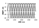
- FIG. 4 is a characteristic diagram showing the calculation result of the transmission spectrum of the arrayed waveguide diffraction grating in the optical waveguide chip 101.
- FIG. 4 is a characteristic diagram showing the calculation result of the transmission spectrum of the arrayed waveguide diffraction grating in the optical waveguide chip 101.
- FIG. 5A is a perspective view showing the configuration of the wavelength checker according to the second embodiment of the present invention.
- FIG. 5B is a side view showing a partial configuration of the wavelength checker according to the second embodiment of the present invention.
- FIG. 5C is a plan view showing a partial configuration of the wavelength checker according to the second embodiment of the present invention.
- FIG. 6A is a perspective view showing a partial configuration of the wavelength checker according to the second embodiment of the present invention.
- FIG. 6B is a sectional view showing a partial configuration of the wavelength checker according to the second embodiment of the present invention.
- FIG. 7A is a sectional view for explaining the manufacturing method for the optical sub-waveguide chip constituting the wavelength checker according to the second embodiment of the present invention.
- FIG. 7B is a sectional view for explaining the manufacturing method for the sub-optical waveguide chip forming the wavelength checker according to the second embodiment of the present invention.
- FIG. 7C is a sectional view for explaining the method for manufacturing the optical sub-waveguide chip constituting the wavelength checker according to the second embodiment of the present invention.
- FIG. 7D is a sectional view for explaining the manufacturing method for the optical sub-waveguide chip constituting the wavelength checker according to the second embodiment of the present invention.
- FIG. 7E is a sectional view for explaining the manufacturing method for the optical sub-waveguide chip constituting the wavelength checker according to the second embodiment of the present invention.
- FIG. 8 is a cross-sectional view showing the configuration in the vicinity of the light conversion section of the wavelength checker according to the second embodiment of the present invention.
- FIG. 9 is a characteristic diagram in which the equation (7) is plotted.
- FIG. 10 is a plan view showing a partial configuration of another wavelength checker according to the second embodiment of the present invention.
- FIG. 11 is a plan view showing a partial configuration of another wavelength checker according to the second embodiment of the present invention.
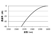
- FIG. 12 is a characteristic diagram showing the calculation result of the transmission spectrum of the arrayed waveguide diffraction grating in the child optical waveguide chip 121a.
- FIG. 13 is a characteristic diagram showing the calculation result of the transmission spectrum of the arrayed waveguide diffraction grating of the optical waveguide chip 101.
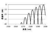
- FIG. 14 is a characteristic diagram showing a spectrum obtained by combining the spectrum shown in FIG. 12 and the spectrum shown in FIG. FIG.
- FIG. 15 is a plan view showing a partial configuration of the wavelength checker according to the third embodiment of the present invention.
- FIG. 16A is a plan view showing a partial configuration of the wavelength checker according to the third embodiment of the present invention.
- FIG. 16B is a plan view showing a partial configuration of the wavelength checker according to the third embodiment of the present invention.
- FIG. 17A is a characteristic diagram showing a calculation result of a spectrum which is input from the main input waveguide 106a of the optical waveguide chip 101a and is transmitted through the arrayed waveguide diffraction grating.
- FIG. 17B is a characteristic diagram showing a calculation result of a spectrum which is input from the sub-input waveguide 106b of the optical waveguide chip 101a and is transmitted through the arrayed waveguide diffraction grating.
- FIG. 18 is a characteristic diagram showing a spectrum obtained by combining the spectrum shown in FIG. 17A and the spectrum shown in FIG. 17B.
- FIG. 19 is a plan view showing a partial configuration of the wavelength checker according to the fourth embodiment of the present invention.
- FIG. 20 is a characteristic diagram showing the calculation result of the transmission spectrum of the optical waveguide chip 101a + the child optical waveguide chip 121a.
- FIG. 21 is a characteristic diagram showing the calculation result of the transmission spectrum of the port 7 of the optical waveguide chip 101a.
- FIG. 22 shows the optical waveguide chip 101a and the secondary optical waveguide chip 121a transparent when the second input waveguide 128 of the secondary optical waveguide chip 121a is connected to the port 7 of the output waveguide 107 of the optical waveguide chip 101a.
- FIG. 23 is a characteristic diagram showing the calculation result of the transmission spectrum of the port 6 of the optical waveguide chip 101a.
- FIG. 24 shows that the arrayed-waveguide diffraction grating of the optical waveguide chip 101a receives light from the sub-input waveguide 106b, the output waveguide 107 of the optical waveguide chip 101a is provided with the port 6, and the sub-optical waveguide chip 121a with the first optical waveguide chip 121a.
- FIG. 25 is a characteristic diagram showing a spectrum obtained by synthesizing the spectrum of FIG. 20, the spectrum of FIG. 22, and the spectrum of FIG.
- FIG. 26 is a plan view showing a partial configuration of the wavelength checker according to the fifth embodiment of the present invention.
- FIG. 27 is an explanatory diagram for explaining the relationship of wavelength arrangement of NG-PON 2, 10G-EPON (XG-PON), and GE-PON (G-PON).
- the wavelength checker according to the embodiment of the present invention will be described below.
- This wavelength checker includes an optical waveguide chip 101.
- a known arrayed waveguide diffraction grating is formed on the optical waveguide chip 101 (see Patent Document 1).
- This arrayed waveguide diffraction grating includes a first arrayed waveguide 103, a first input-side slab waveguide 104, a first output-side slab waveguide 105, a first input waveguide 106, and a first output waveguide 107.
- Reference numeral 151 is a main substrate
- reference numeral 109 is a support portion
- reference numeral 102 is a light conversion portion made of a conversion material that converts near-infrared light into visible light.
- Reference numeral 161 is a fiber block
- reference numeral 162 is an optical fiber
- reference numeral 163 is a connector.
- the first arrayed waveguide 103 is composed of a plurality of waveguides having a constant optical path length difference. In the first arrayed waveguide 103, the optical path length difference between two adjacent waveguides is constant.
- the first input-side slab waveguide 104 is connected to the light input end of the first arrayed waveguide 103.
- the first output-side slab waveguide 105 is connected to the optical output end of the first arrayed waveguide 103.
- the first input waveguide 106 is connected to the input side of the first input-side slab waveguide 104.
- a plurality of first output waveguides 107 are provided and are connected to the output side of the first output side slab waveguide 105.
- the wavelength checker also includes a light conversion unit 102 made of a conversion material that converts infrared light into visible light.
- the light conversion unit 102 is arranged on the output side of the plurality of output waveguides 107 of the optical waveguide chip 101 so as to be able to receive the emitted light emitted from the plurality of output waveguides 107.
- the light conversion section 102 is formed to extend in the direction in which the plurality of output waveguides 107 are arranged.
- the light conversion unit 102 extends, for example, from one end side to the other end side of the array of the plurality of output waveguides 107.
- the conversion material is, for example, a phosphor or a phosphor that converts near-infrared light into visible light.
- the conversion material can be mixed with a thermosetting silicone resin and heated to be cured to form the light conversion section 102.
- a thermosetting silicone resin for example, Phosphor manufactured by "Lumitek International" can be used.
- some conversion materials have a sensitivity between 700 nm and 1700 nm.
- the near-infrared light demultiplexed for each wavelength by the arrayed waveguide diffraction grating, guided through the first output waveguide 107, and emitted from the output end 108 is a light conversion unit.
- visible light is generated.
- the generated visible light is not limited to the incident direction of the near-infrared light emitted from the output end 108, but isotropically spreads and can be viewed from various directions.
- the first output waveguide 107 from which the near-infrared light is emitted can be specified from the place where the visible light is generated. Since the wavelength of the near-infrared light demultiplexed and guided to each of the first output waveguides 107 is known, the wavelength can be confirmed by confirming the location where visible light is generated (visually observed). It will be possible.
- the first input-side slab waveguide 104 includes a lower clad layer 112 formed on a Si substrate 111 made of, for example, Si, and a core formed on the lower clad layer 112. It is composed of a portion 104a and an upper clad layer 113 formed on the core portion 104a.
- FIG. 2A shows a cross section taken along the line aa ′ in FIG. 1. 2A, the main substrate 151 below the Si substrate 111 is omitted.
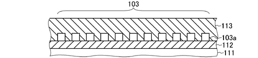
- the first arrayed waveguide 103 includes a lower clad layer 112 formed on the Si substrate 111, a plurality of core portions 103a formed on the lower clad layer 112, and a plurality of core portions 103a. And an upper clad layer 113 formed on the core portion 103a.
- FIG. 2B shows a cross section taken along the line bb 'of FIG.
- the Si substrate 111 is a silicon substrate
- each clad layer is made of silica glass
- the core portions 103a and 104a are made of silica glass.
- the main substrate 151 below the Si substrate 111 is omitted.
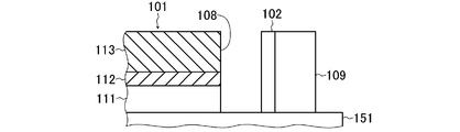
- the light conversion section 102 is formed on the side surface of the support section 109 facing the output end surface 108 of the optical waveguide chip 101.
- the support 109 is fixed to the main board 151.
- FIG. 2C shows a cross section taken along line cc ′ of FIG.
- the arrayed waveguide diffraction grating will be described in more detail.
- the case where the first arrayed waveguide 103 is composed of eight waveguides and includes eight first output waveguides 107 will be described as an example (in FIG. 1, it is composed of eleven waveguides). However, in reality there are many more).
- the multiplexed light of eight wavelengths input to the first input waveguide 106 is branched into eight outputs.
- the multiplexed light input to the first input waveguide 106 is diffracted and spread in the first input side slab waveguide 104, and each of these is coupled to each waveguide of the first array waveguide 103 and guided.
- the first arrayed waveguide 103 has a long optical path length on the upper side (outer side) of the paper surface of FIG. 1, and has a shorter optical path length at the same distance as it goes to the lower side (inner side) of the paper surface of FIG.
- At the end of the first arrayed waveguide 103 there is a phase difference from the outer side to the inner side of the first arrayed waveguide 103.
- the inclination of the fan-shaped equiphase surface caused by the shape of the slab waveguide changes depending on the wavelength, and the corresponding first output waveguide 107 for each wavelength. Will be focused (optically coupled) to.
- the arrayed-waveguide diffraction grating it is possible to split (demultiplex) the wavelength-multiplexed light for each wavelength.
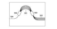
- the arrayed waveguide 501 is bent at one place like an arc in a plan view.
- reference numeral 502 is an input side slab waveguide
- reference numeral 503 is an output side slab waveguide
- reference numeral 504 is an input waveguide
- reference numeral 505 is an output waveguide.
- the first arrayed waveguide 103 is bent at a plurality of points in a plan view and has a shape like a seagull wing in a plan view. This point will be described later.
- the optical path lengths of the respective waveguides forming the first arrayed waveguide 103 of the arrayed waveguide diffraction grating in the embodiment will be described in detail.
- the center wavelength ⁇ 0 of the arrayed waveguide diffraction grating is expressed by the following equation (1).
- the center wavelength ⁇ 0 is usually the transmission center wavelength of the center port of the output ports of the arrayed waveguide grating.
- n c represents the effective refractive index of the arrayed waveguide
- m represents the diffraction order.
- the output end of the uppermost first output waveguide 107 is port 1
- the output end of the second output first output waveguide 107 is port 2
- the output end of the output waveguide 107 is the port 3
- the output end of the first output waveguide 107 of the fourth stage is the port 4
- the output end of the first output waveguide 107 of the fifth stage is the port 5 and the output end of the sixth stage.
- the output end of the first output waveguide 107 is port 6, the output end of the first output waveguide 107 at the seventh stage is port 7, and the output end of the first output waveguide 107 at the eighth stage is port 8.
- the free spectral range (FSR) of the arrayed waveguide diffraction grating is expressed by the following equation (2).
- Non-Patent Document 2 and Non-Patent Document 3 for Formula (1) and Formula (2).
- the free spectral range (FSR) of the arrayed waveguide diffraction grating is set to 400 nm or more of wavelengths from 1250 nm to 1650 nm
- the center wavelength ⁇ 0 is designed to be 1450 nm
- the wavelength interval is 50 nm
- the first output waveguide 107 is designed to be eight.
- the entire wavelength range of the access PON system can be covered.
- the center wavelength of FSR is 1450 nm, it is sufficient to set the diffraction order m to any one of 1 to 3 from the equation (2).
- the optical path length difference ⁇ L becomes a minute length on the order of ⁇ m, which cannot be realized in the arc structure in which the first arrayed waveguide 103 is bent at only one place. Therefore, in the embodiment, the first arrayed waveguide 103 has a structure in which the first arrayed waveguide 103 is bent at a plurality of points in the central portion and the portions on both sides (both sides) in plan view. In this way, by providing a plurality of bent portions, the change in the optical path length from the upper side (outer side) of the paper surface of FIG. 1 to the side (inner side) of the paper surface of FIG. 1 at different bent portions of the first arrayed waveguide 103. Can be reversed.
- the first arrayed waveguide 103 is bent so as to be convex outward in plan view at the central portion, and is bent inward so as to be convex in plan view at both sides sandwiching the central portion.
- the optical path length becomes longer toward the outside (upper side of the paper in FIG. 1), but at both side portions, the optical path length becomes shorter toward the outside. ..
- the optical path length difference between adjacent waveguides in the central portion of the first arrayed waveguide 103 and the adjacent optical path length difference in both side portions are set to different values, and the optical path length changes between the central portion and both side portions to some extent. By canceling each other, it becomes possible to set a small optical path length difference in the entire first arrayed waveguide 103.
- the detailed design of the above-mentioned optical path length difference is described in Patent Document 1.
- the transmission spectrum function of the arrayed waveguide diffraction grating (optical waveguide chip 101) is expressed by a Gaussian function.
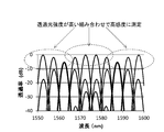
- An example of the calculation result is shown in FIG.
- the transmission center wavelength of the output port 1 is 1275 nm.
- the transmission center wavelength of the output port 2 is 1325 nm.
- the transmission center wavelength of the output port 3 is 1375 nm.
- the transmission center wavelength of the output port 4 is 1425 nm.
- the transmission center wavelength of the output port 5 is 1475 nm.
- the transmission center wavelength of the output port 6 is 1525 nm.
- the transmission center wavelength of the output port 7 is 1575 nm.
- the transmission center wavelength of the output port 8 is 1625 nm.
- ⁇ f is the deviation from the transmission center frequency
- ⁇ x is the distance between the center positions of the first output waveguides 107 connected to the first output-side slab waveguide 105
- ⁇ f is the center between adjacent channels.
- the frequency interval, ⁇ 0, is the spot size.
- Equation (3) represented in the frequency domain is represented in the wavelength domain by equation (5).
- FIG. 4 shows the result of calculating the transmission spectrum of each channel of the arrayed waveguide diffraction grating by using the equation (5).
- the parameter ⁇ x / ⁇ 0 representing the steepness of the Gaussian function can be adjusted when designing the arrayed waveguide diffraction grating, and this parameter ⁇ x / ⁇ 0 is set to 4.5 in the embodiment.
- the wavelength range is as wide as 1250 nm to 1650 nm, there is a loss around 1380 nm in the arrayed waveguide diffraction grating of this design due to the absorption of OH groups in the silica glass forming the waveguide.
- this wavelength band is not used for transmission, it does not affect the operating characteristics of the arrayed waveguide diffraction grating.
- the calculation result shown in FIG. 4 does not consider the calculation regarding the absorption of the OH group in the silica glass forming the waveguide.
- the above-mentioned arrayed-waveguide diffraction grating has a channel interval of 50 nm, but the temperature dependence of the demultiplexing wavelength of the interference type filter using the silica-based waveguide is 0.01 nm / ° C. Even if the indoor / outdoor use environment temperature changes from -5 ° C to 35 ° C at 40 ° C, the wavelength variation corresponds to about 0.4 nm due to the above temperature dependency, which is 1/100 or less of the interval between adjacent channels. , The demultiplexing characteristic is not affected. Therefore, when actually using the above-mentioned arrayed-waveguide diffraction grating, it is not necessary to control the temperature by using a Peltier element or the like.
- This wavelength checker includes an optical waveguide chip 101.
- the optical waveguide chip 101 is similar to that of the first embodiment described above.
- the wavelength checker includes an optical waveguide chip 121 that is arranged side by side with the optical waveguide chip 101 and that includes an optical waveguide that guides outgoing light.
- the optical waveguide chip 121 is formed with a plurality of linear optical waveguides. For example, eight linear optical waveguides are formed on the optical waveguide chip 121 corresponding to the eight output waveguides of the optical waveguide chip 101. Further, eight linear optical waveguides are arranged at the same 1 mm intervals as the intervals between the output ends of the eight output waveguides of the optical waveguide chip 101.
- the surface of the light conversion unit 102 that is irradiated with the emitted light is arranged to face the output end of the optical waveguide chip 121 that outputs the emitted light to the outside.
- the light conversion unit 102 is similar to that of the first embodiment described above.
- the optical waveguide chip 121 is arranged in series in the optical waveguide chip 101 in the waveguide direction.
- the optical waveguide chip 101 and the optical waveguide chip 121 are mounted on the optical waveguide chip 141. That is, they are laminated in two layers.
- the lower optical waveguide chip is defined as a parent optical waveguide chip
- the upper optical waveguide chip is defined as a child optical waveguide chip. Therefore, in the following, they are referred to as the child optical waveguide chip 101, the child optical waveguide chip 121, and the parent optical waveguide chip 141.
- the parent optical waveguide chip 141 may have a planar lightwave circuit or may have no optical circuit (only the clad glass is on the Si substrate).
- the surface on which each optical waveguide (planar lightwave circuit) is formed (the surface on which the clad glass is present) ) Is mounted on the parent optical waveguide chip 141 via a spacer (not shown).
- the optical waveguide chip that tries to transmit light is a child optical waveguide chip.
- the surface with the clad glass is taken as the front surface, the back surface with the Si substrate is visible when viewed from above the child waveguide chip. That is, in the sub-optical waveguide chip, the portion of the optical circuit composed of the core and the clad comes to the lower side.
- the parent optical waveguide chip 141 is mounted on the main board 151.
- the parent optical waveguide chip 141 is adhered and fixed on the main substrate 151 with an adhesive.
- the child optical waveguide chip 101 and the child optical waveguide chip 121 are arranged side by side in a column along the light input direction.
- the light conversion section 102 is supported by a support section 109 fixed on the main substrate 151.
- the light conversion section 102 can be formed by applying a conversion material that converts infrared light into visible light on the side surface of the support section 109 facing the output end surface of the child optical waveguide chip 121.
- a fiber block 161 is connected to the input waveguide end of the child optical waveguide chip 101.
- An optical fiber 162 provided with a connector 163 for inputting an optical signal to be confirmed is connected to the fiber block 161.
- An optical fiber with a connector (not shown) is separately used for aligning the fiber block 161 and the input waveguide of the sub optical waveguide chip 101.
- the child optical waveguide chip 101 is fixed to the parent optical waveguide chip 141 by an adhesive agent via a spacer (not shown).
- the child optical waveguide chip 121 is attachable to and detachable from the parent optical waveguide chip 141 in a semi-fixed state.
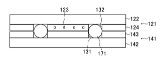
- each of the plurality of first grooves 131 has a plurality of spacer members 171 fitted therein such that a part thereof protrudes from the parent optical waveguide chip 141.
- each of the second groove 132 of the child optical waveguide chip 101 and the second groove 132 of the child optical waveguide chip 121 is also fitted to the protruding portion of any one of the plurality of spacer members 171.
- the position of the second groove 132 is arranged so as to avoid the waveguide portion (core) portion of the child optical waveguide chip 101 and the child optical waveguide chip 121.
- the number of grooves is usually 3 or more.
- the first groove 131 is formed in the clad layer 143 of the parent optical waveguide chip 141.
- the first groove 131 penetrates the clad layer 143, reaches the substrate 142, and is formed.
- the second groove 132 is formed in the clad layer 124 including the core 123 of the child optical waveguide chip 121.
- the second groove 132 penetrates the clad layer 124, reaches the substrate 122, and is formed.
- the first groove 131 and the second groove 132 can be formed by known photolithography technology and etching technology (reactive ion etching, etc.).
- the first groove 131 is formed by etching the clad layer 143 using the substrate 142 as an etching stop layer using the mask pattern formed by the photolithography technique as a mask.
- the second groove 132 is formed by etching the clad layer 124 using the substrate 122 as an etching stop layer using the mask pattern formed by the photolithography technique as a mask.
- the positional accuracy (deviation amount) in the surface direction with respect to the design of the first groove 131 and the second groove 132 formed in this way is determined by the positional accuracy of the mask pattern and the positional deviation amount during etching.
- the positional accuracy of a mask pattern is submicron or less, and the positional deviation in reactive ion etching is also submicron or less. Therefore, the position in the surface direction where the first groove 131 and the second groove 132 are formed is 1 ⁇ m or less with respect to the design.
- the depth of the first groove 131 is determined by the thickness of the clad layer 143, and the depth of the second groove 132 is determined by the thickness of the clad layer 124.
- the accuracy of the thickness of the clad layer 143 and the accuracy of the thickness of the clad layer 124 are determined in the submicron order, for example, by a well-known glass deposition technique. The same applies to the position in the thickness direction of the core 123 embedded in the clad layer 124.
- the spacer member 171 can be formed, for example, by cutting an optical fiber into a predetermined length, and the accuracy of the diameter of each spacer member 171 can be determined in the submicron order. Therefore, the positional accuracy of the child optical waveguide chip 121 in the thickness direction is also determined within 1 ⁇ m.
- the child optical waveguide chip 101 and the child optical waveguide chip 121 mounted on the parent optical waveguide chip 141 can accurately match the positions of the core centers of the corresponding optical waveguides. it can.
- the alignment between a plurality of child chips mounted on the above-described optical parent chip is performed under the condition that no warpage occurs in each chip.
- Patent Document 2 Non-Patent Document 4, and Non-Patent Document 5.
- This optical mounting form is called a PPCP (Pluggable Photonic Circuit Platform).
- the sub-optical waveguide chip 121 mounted by PPCP is characterized in that it is removable. Therefore, the sub-optical waveguide chips 121 having various functions can be replaced and used, and various functions can be flexibly provided. It can be said that PPCP has the characteristics of an optical circuit (optical chip) version of an electronic block.
- a substrate 122 made of Si is prepared.
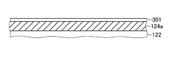
- the lower clad layer 124a is formed on the substrate 122, and the core forming layer 301 is formed on the lower clad layer 124a.
- the lower clad layer 124a and the core forming layer 301 can be formed by the flame deposition (FHD) method.
- a raw material gas main component: silicon tetrachloride
- heated and hydrolyzed glass fine particles are deposited on the substrate 122 to form a first fine particle layer to be the lower cladding layer 124a. ..
- glass particles having different compositions are deposited on the first particle layer to form the second particle layer to be the core forming layer 301. ..
- the first fine particle layer and the second fine particle layer are heated using an electric furnace or the like to form a transparent glass composition film, thereby forming the lower clad layer 124a and the core forming layer. It is 301. Note that these layers can also be formed by a chemical vapor deposition method.
- the core 123 is formed by patterning the core forming layer 301 by a known lithography technique and etching technique used for manufacturing a semiconductor device. For example, a resist pattern is formed on the core forming layer 301 on the portion to be the core 123 by photolithography. Next, using the formed resist pattern as a mask, the core forming layer 301 is etched by reactive ion etching (RIE), and the other core forming layers are removed leaving a portion to be the core 123. After that, if the resist pattern is removed, the core 123 can be formed.
- RIE reactive ion etching
- the upper clad layer 124b is formed on the core 123. Similar to the lower clad layer 124a described above, the upper clad layer 124b can be formed by the FHD method.
- the upper clad layer 124b and the lower clad layer 124a are penetrated to reach the substrate 122 as shown in FIG. 7E.
- the second groove 132 is formed.
- a photolithography technique is used to form a resist pattern having an opening at the location where the second groove 132 is to be formed, on the upper cladding layer 124b.
- the upper clad layer 124b and the lower clad layer 124a are etched by RIE to remove the portion to be the second groove 132. After that, if the resist pattern is removed, the second groove 132 can be formed.
- FIG. 8 shows an enlarged cross section of the emission part of the sub optical waveguide chip 121.
- MFD mode field diameter
- spot size 3 ⁇ m the mode field diameter
- the mode field diameter is, for example, approximately 4.5 ⁇ m ⁇ 4.5 ⁇ m (rectangle) of the cross section of the core, and the mode field diameter realized by an optical waveguide having a relative refractive index difference of 1.5% between the core and the clad is approximately.
- the spot size is half of the MFD.
- the beam spread is calculated by approximating the electric field distribution in the optical waveguide as a Gaussian distribution.
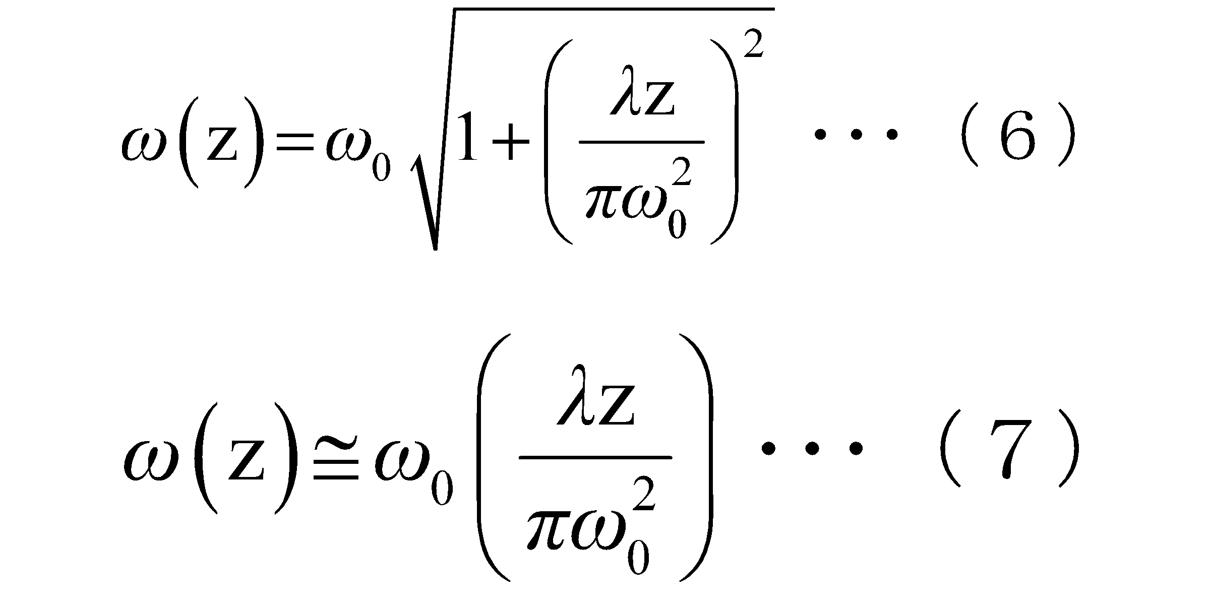
- the spot size at the exit end is ⁇ 0
- the beam diameter after propagating a distance z from the exit end face is expressed by equation (6). This is described in detail in Non-Patent Document 6.
- ⁇ is the wavelength.
- the expression (6) can be approximated by the expression (7) under the condition that the square term in ⁇ of the expression (6) is sufficiently larger than 1 (in this case, z> 100 ⁇ m).
- the end surface of the child optical waveguide chip 121 on the emitting side is
- the parent optical waveguide chip 141 is farther from the optical conversion unit 102 than the end surface on the optical conversion unit 102 side
- the emitted light of the child optical waveguide chip 121 causes the parent optical waveguide chip 141 to emit light from the cladding layer 143 and the substrate 142.
- the light enters the portion and is refracted, and the shape of the beam applied to the light conversion unit 102 is deformed, making it difficult to recognize.
- the refractive index of air is 1
- the refractive index of silica glass that controls the cladding is 1.4-1.5
- the refractive index of Si that composes the substrate is 3.5, which is a large difference. The corners are even bigger.
- the end surface of the child optical waveguide chip 121 on the emission side (the side of the light conversion section 102) is located at the same position as the end surface of the parent optical waveguide chip 141 on the side of the light conversion section 102 and on the side of the light conversion section 102. It is important that the parent optical waveguide chip 141 is arranged closer to the light conversion section 102 than the end surface of the parent optical waveguide chip 141 on the light conversion section 102 side.
- the transmission spectrum of the child optical waveguide chip 121 is similar to that of the first embodiment, and is shown in FIG. A spectrum is obtained.
- the sub optical waveguide chip 121a includes an arrayed waveguide diffraction grating having a narrow wavelength separation.
- reference numeral 125 is the second array waveguide
- reference numeral 126 is the second input slab waveguide
- reference numeral 127 is the second output slab waveguide
- reference numeral 128 is the second input waveguide
- reference numeral 129 Indicate the second output waveguides, respectively.
- This is a normal arrayed waveguide diffraction grating in which the second arrayed waveguide 125 has an arc shape in a plan view.
- a part of the second output waveguide 129 is omitted.
- FIG. 11 shows a connection state between the child optical waveguide chip 101 and the child optical waveguide chip 121a.
- FIG. 11 shows a connection state between the child optical waveguide chip 101 and the child optical waveguide chip 121a.
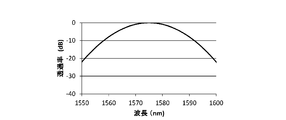
- FIG. 12 shows a transmission wavelength spectrum of the arrayed-waveguide diffraction grating (with a narrow demultiplexing wavelength interval) of the sub-optical waveguide chip 121 in this case. This spectrum is the result of calculation using equation (5).
- the transmission spectrum of the arrayed waveguide diffraction grating of the child optical waveguide chip 101 becomes a broad spectrum as shown in FIG.
- the transmission spectrum in the configuration in which the sub-optical waveguide chip 101 and the sub-optical waveguide chip 121a are connected is a combination of the spectrum shown in FIG. 12 and the spectrum shown in FIG. 13, so that the spectrum shown in FIG. 14 is obtained.
- the transmission spectrum when the sub optical waveguide chip 101 is combined with the sub optical waveguide chip 121 composed of a linear optical waveguide is shown in FIG. 4, and the wavelength resolution is 50 nm.
- the wavelength resolution is 5 nm, and the wavelength can be confirmed with higher precision. ..
- the subordinate range is a wide band of 400 nm from 1250 nm to 1650 nm.
- the band becomes narrow as shown in FIG.
- the sub-optical waveguide chip 121 and the sub-optical waveguide chip 121a interchangeable by implementing the PPCP, it becomes possible to flexibly change the wavelength resolution and measurement range of the wavelength checker.
- the wavelength in the wavelength region of wavelengths from 1550 nm to 1600 nm, the wavelength is confirmed more finely by using the arrayed waveguide diffraction grating with a narrow wavelength interval. If an arrayed waveguide diffraction grating with 5 nm intervals and 10 ports corresponding to the wavelength range output from this is prepared and connected to another output port of the grating, the wavelength can be confirmed with a wavelength resolution of 5 nm in other wavelength ranges. Recognize.
- a device having a free spectral range (FSR) equal to the channel interval ⁇ the number of channels is called a cyclic array waveguide diffraction grating (circular array waveguide diffraction grating). If the above-mentioned circular array waveguide diffraction grating is used for the array waveguide diffraction grating with a narrow wavelength interval, the optical chip connected to the sub optical waveguide chip 101 can be shared by the same circular array waveguide diffraction grating. ..
- wavelengths are demultiplexed for each wavelength by an arrayed waveguide diffraction grating, and a material (wavelength conversion material) that converts near-infrared light into visible light is irradiated and shines.
- An inspection method for visually confirming the wavelength from the port can also be proposed.
- the broad interpretation of the arrayed waveguide diffraction grating is the diffraction grating (grating).
- the wavelength is divided into wavelengths by the diffraction grating (grating), the wavelength conversion material is irradiated, and the wavelength is visually checked from the illuminated position.
- An inspection method to confirm can also be proposed. These inspection methods have a feature that the wavelength inspection can be easily performed without using a power source or the like.
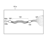
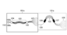
- the child optical waveguide chip 101a shown in FIG. 15 is used instead of the child optical waveguide chip 101.
- the main first input waveguide 106a and the sub first input waveguide 106b are connected to the input side of the first input side slab waveguide 104.
- Other configurations are similar to those of the sub optical waveguide chip 101.
- the first input-side slab waveguide 104 of the main first input waveguide 106a is ⁇ x out .
- the waveguide interval between the connection portion with and the connection portion with the first input side slab waveguide 104 of the sub-first input waveguide 106b is ⁇ x out / 2.
- the first input side slab waveguide 104, the first array waveguide 103, and the first output side slab waveguide 105 have a shape in plan view that is the first input side slab waveguide 104.
- the first input-side slab waveguide 104 has an arc having the same curvature on the side in contact with the input waveguide and the side in contact with the array waveguide. Therefore, the center of the input-side slab waveguide is the intersection of the straight lines that make up the outer shape of the slab waveguide and the straight line that connects the four points where the arcs intersect. The same applies to the first output-side slab waveguide 105.
- the wavelength-multiplexed light input to the sub-first input waveguide 106b is supplied to each of the first output waveguides 107.
- the transmission center wavelength is branched into ⁇ 2, ⁇ 3, ⁇ 4, ... ⁇ 9 at equal intervals. This is because the sub-first input waveguide 106b is displaced by one, so the wavefront when reaching the first arrayed waveguide 103 is tilted, and as a result, the wavefront when reaching the first output waveguide 107 is tilted, This is because the same wavelength is focused on the first output waveguide 107 which is shifted by one.
- the spectrum (calculated value) input from the main first input waveguide 106a and transmitted through the arrayed waveguide diffraction grating is: As shown in FIG. 17A, the spectrum is the same as the transmission spectrum of the child optical waveguide chip 101. That is, the transmission center wavelength of each of the first output waveguides 107 is 1275 nm, 1325 nm, 1375 nm, 1425 nm, 1475 nm, 1525 nm, 1575 nm, 1625 nm.
- the spectrum (calculated value) that is input from the sub first input waveguide 106b and transmitted through the arrayed waveguide diffraction grating is shifted by half the wavelength interval, and is 1300 nm, 1350 nm, 1400 nm, and 1450 nm. 1500 nm, 1550 nm, 1600 nm, and 1650 nm. That is, the transmission spectrum from the main first input waveguide 106a and the spectrum from the sub first input waveguide 106b are staggered.
- the effects of the main first input waveguide 106a and the sub first input waveguide 106b are as follows.
- the number of the input waveguides is one, when the light having the wavelength between the transmission spectra of the adjacent first output waveguides 107 is input, the transmittance is low, so that the near infrared light is changed to the visible light.
- the converted light is also weak, and light emission in the light conversion unit 102 may not be recognized.
- the transmitted light intensity at port 1 and port 2 at the wavelength of 1300 nm in FIG. 17A is degraded by 20 dB as compared with the most transmitted wavelength (wavelength of 1275 nm or 1325 nm).
- the main first input waveguide 106a and the sub first input waveguide 106b are used, by inputting the signal light also to the sub first input waveguide 106b, the transmitted light intensity of the port 1 at the wavelength of 1300 nm is , The wavelength that is most transmitted.
- the main first input waveguide 106a and the sub first input waveguide 106b as shown in FIG. 18 where FIG. 17A and FIG. It can be seen that the deterioration is 5 dB (excluding around the wavelength of 1250 nm).
- the main first input waveguide 106a and the sub-first input waveguide 106b are used for both.
- a wavelength checker according to the fourth embodiment of the present invention will be described with reference to FIG.
- a child optical waveguide chip 101a shown in FIG. instead of the optical waveguide chip 121, a child optical waveguide chip 121a including an arrayed waveguide diffraction grating having a narrow demultiplexing wavelength interval is used.
- the arrayed-waveguide diffraction grating of the sub-optical waveguide chip 121a is an arrayed-waveguide diffraction grating having a demultiplexing wavelength of 1550 nm to 1600 nm and a demultiplexing wavelength interval of 5 nm and 10 ports.
- the first output waveguide 107 of the child optical waveguide chip 101a is considered.
- the second input waveguide 128 of the child optical waveguide chip 121a is connected to the port 7.
- the transmission wavelength spectrum of the arrayed waveguide diffraction grating of the sub optical waveguide chip 121a is as shown in FIG. 12, and the transmission spectrum of the sub optical waveguide chip 101a + the sub optical waveguide chip 121a is the spectrum as shown in FIG. 20, as in the above description. become.
- the port 7 is provided in the first output waveguide 107 of the child optical waveguide chip 101a.
- the transmission spectrum of the port 7 of the secondary optical waveguide chip 101a is as shown in FIG. It can be seen from the transmission spectrum (FIG. 13) in the case where light is input from the main first input waveguide 106a, the spectrum shown in FIG. 21 is shifted to a long wave by a half wavelength interval (25 nm).
- the transmission spectrum of the child optical waveguide chip 121a is shown in FIG. 12, the spectrum transmitted through the child optical waveguide chip 101a and the child optical waveguide chip 121a is shown in FIG.
- the port 6 is provided in the first output waveguide 107 of the sub optical waveguide chip 101a.
- the transmission spectrum of the port 6 of the sub optical waveguide chip 101a is expressed as shown in FIG.
- the spectrum shown in FIG. 23 is shifted to a shorter wave by the wavelength interval than the spectrum shown in FIG.
- the transmission spectrum of the child optical waveguide chip 121a is shown in FIG. 12
- the spectrum transmitted through the child optical waveguide chip 101a and the child optical waveguide chip 121a is shown in FIG.
- the transmission spectra using the main first input waveguide 106a and the sub first input waveguide 106b of the child optical waveguide chip 101a are the spectra of FIG. 20, the spectra of FIG. 22, and the spectra of FIG. The spectrum shown in FIG.
- the transmission spectrum of the child optical waveguide chip 101 + the child optical waveguide chip 121a is as shown in FIG. 14, and shows a high transmittance at wavelengths of 1570 nm to 1580 nm, but the transmittance is low near 1550 and 1600 nm, and the signal light is recognized. It may not be possible.
- the synthetic transmission spectrum is as shown in FIG. 25, and the transmittance is increased even in the vicinity of 1550 nm and 1600 nm so that the wavelength range in which the signal light can be recognized can be widened. become.
- the sub-optical waveguide chip 101a including the two main first input waveguides 106a and the sub-first input waveguide 106b is used to widen the wavelength region having high transmittance. Also in the arrayed waveguide diffraction grating of No. 2, it is possible to further widen the wavelength region having high transmittance by using two input waveguides.
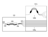
- a wavelength checker according to the fifth embodiment of the present invention will be described with reference to FIG.
- an optical waveguide portion 120a composed of a linear optical waveguide and an arrayed waveguide diffraction grating 120b having a narrow demultiplexed wavelength interval are provided.
- the optical sub-waveguide chip 121b provided with is used.
- An additional groove for fitting with the child optical waveguide chip 121b is provided in the parent optical chip on which the child optical waveguide chip 101 and the child optical waveguide chip 121b are mounted, so that the child optical waveguide chip 121b is perpendicular to the optical waveguide direction. It can be moved in any direction. By doing so, the child optical waveguide chip 121b is slid on the parent optical chip, and the child optical waveguide chip 121b is moved to connect the child optical waveguide chip 101 and the optical waveguide section 120a, and The connection between the waveguide chip 101 and the arrayed waveguide diffraction grating 120b can be switched.
- one child optical waveguide chip 121b may be prepared. It has the effect of reducing the number of parts.
- the arrayed waveguide diffraction grating of the child optical waveguide chip 121a it is necessary to prepare a separate arrayed waveguide diffraction grating when the wavelength bands are different, but according to the fifth embodiment, for example, the inspection resolution is increased.
- the arrayed-waveguide diffraction grating required for the wavelength region may be inserted in the sub-optical waveguide chip 121b within a range allowed by the chip space.
- the light conversion part formed of the conversion material that converts infrared light into visible light is placed on the output side of the plurality of first output waveguides of the optical waveguide chip. Since the emitted light emitted from the plurality of first output waveguides is arranged so as to be able to receive the light, it is possible to easily confirm the presence or absence of the signal light when the PON system is opened and when the failure is isolated.
Landscapes
- Physics & Mathematics (AREA)
- General Physics & Mathematics (AREA)
- Optics & Photonics (AREA)
- Engineering & Computer Science (AREA)
- Microelectronics & Electronic Packaging (AREA)
- Electromagnetism (AREA)
- Spectroscopy & Molecular Physics (AREA)
- Computer Networks & Wireless Communication (AREA)
- Signal Processing (AREA)
- Optical Integrated Circuits (AREA)
- Photometry And Measurement Of Optical Pulse Characteristics (AREA)
- Mechanical Coupling Of Light Guides (AREA)
- Optical Couplings Of Light Guides (AREA)
- Optical Communication System (AREA)
Abstract
この波長チェッカーは、光導波路チップ(101)を備える。光導波路チップ(101)には、公知のアレイ導波路回折格子が形成されている。また、この波長チェッカーは、赤外光を可視光に変換する変換材料から構成された光変換部(102)を備える。光変換部(102)は、光導波路チップ(101)の複数の第1出力導波路(107)の出力側に、複数の第1出力導波路(107)より出射される出射光を受光可能に配置されている。光変換部(102)は、支持部(109)において光導波路チップ(101)の出力端面(108)に向かい合った側面に形成されている。なお、支持部(109)は主基板(151)に固定されている。
Description
本発明は、波長チェッカーに関し、より具体的には、PONシステムの開通・故障切り分け調査における信号光の確認など行う波長チェッカーに関する。
光通信システムのアクセス系PON(Passive Optical Network)システムでは、波長1.3μmと波長1.5~1.6μmとなど、波長が比較的離れた複数の光を同時に用いることがある。
非特許文献1によると、すでに導入されているGE-PON(G-PON)システムでは、ユーザから局舎への信号(上り信号)として、1260nm~1360nm(G-PONにおいてはRegular帯域のみ記載)の波長が用いられている。また、G-PONシステムでは、局舎からユーザへの信号(下り信号)として、1480nm~1500nmの波長が用いられ、下りの映像信号としては、1550nm~1560nmの波長が用いられている。
今後、導入される予定の10G-EPON(XG-PON)システムも同様に、波長1.3μmと波長1.5~1.6μmの波長が用いられる。最近標準化が完了したNG-PON2システムでは、上り信号が1524nm~1544nm(Wide帯域)、下り信号が1596nm~1603nm、下りの映像信号が1550nm~1560nmの波長が用いられている。なお、オプションのPtPWDM(Point To Point Wavelength Division Multiplex)オーバーレイは、説明を省略する。このシステムでは、GE-PON(G-PON)、10G-EPON(XG-PON)と異なり、波長多重が行われる。これらの波長配置を、図27に示す。
ところで、GE-PONなどのPONシステムでは、開通試験において、光パワーを確認している。今後、GE-PONから10G-EPONへの移行時には、より多くの様々な波長が用いられるようになる。このような状況における試験では、波長が確認できれば信号の種類が判別でき、故障の切り分けが容易となり、作業効率を上げられる可能性がある。
胡間 遼 他、「PONシステムのさらなる高速化に関する標準化動向」、NTT技術ジャーナル、2017年8月号、51-53頁。
高橋 浩 他、「WDM用アレイ導波路回折格子」、NTT R&D、 vol. 46、no. 7、685-692頁、1997年。
H. Takahashi et al., "Transmission Characteristics of Arrayed Waveguide N×N Wavelength Multiplexer", Journal of Lightwave Technology, vol. 13, no. 3, pp. 447-455, 1995.
H. Ishikawa et al., "Pluggable Photonic Circuit Platform Using a Novel Passive Alignment Method", The Japan Society of Applied Physics, 22nd Microoptics Conference, D-6, pp. 84-85, 2017.
K. Shikama et al., "Pluggable photonic circuit platform for single-mode waveguide connections using novel passive alignment method", Japanese Journal of Applied Physics, vol. 57, 08PC03, 2018.
河野健治 著、「光デバイスのための光結合系の基礎と応用」、現代工学社、初版、1991年。
H. Takahashi et al., "Wavelength Multiplexer Based on SiO2-Ta2O5 Arrayed-Waveguide Grating", IEEE Journal of Lightwave Technology, vol. 12, no. 6, pp. 989-005, 1994.
ところで、波長を測定する手段としては、光スペクトラムアナライザがある。しかしながら、光スペクトラムアナライザは、回折格子を動かして得られる回折光を検出器で検知するための可動部分があるため、装置が大きく、重量が大きいため、可搬性に難があった。また、一般に100Vの電源が必要であるといった欠点もあった。このように、従来では、PONシステムの開通・故障切り分け調査において信号光が来ているかどうかの確認などが、容易に実施できないという問題があった。
本発明は、以上のような問題点を解消するためになされたものであり、PONシステムの開通、故障切り分けなどにおける信号光の有無の確認などが、容易に実施できるようにすることを目的とする。
本発明に係る波長チェッカーは、光導波路チップと近赤外光を可視光に変換する変換材料から構成された光変換部を備える波長チェッカーにおいて、光ファイバーと接続している側の光導波路チップがアレイ導波路回折格子を含み、かつ主基板の上に搭載されており、主基板上に支持部が固定されており、支持部は外部空間に光を出力する側の光導波路チップの光出射端面と対向する位置にあり、光変換部は光出射端面に面している支持部の側面に備えられる。
上記波長チェッカーの一構成例において、光導波路チップは2層に積層され、光導波路チップが基板及び基板上のコアとクラッドもしくは基板及び基板上のクラッドから構成され、クラッド側を光導波路チップの表面と定義すると、積層されている上下層の光導波路チップの表面を対向させ、下層側の光導波路チップを親光導波路チップ、上層側の光導波路チップを子光導波路チップと定義すると、親光導波路チップが1個あり、子光導波路チップが複数あり、親光導波路チップのクラッド部分に複数の第1溝が形成され、子光導波路チップのクラッド部分に複数の第2溝が形成され、数の第1溝の各々は、一部が親光導波路チップから突出した形で複数のスペーサ部材が嵌合し、子光導波路チップの第2溝の各々は、いずれかの複数のスペーサ部材の突出した部分と嵌合し、光ファイバーと接続している側の子光導波路チップは、アレイ導波路回折格子を含み、他の子光導波路チップは直線導波路群もしくはアレイ導波路回折格子の少なくとも一方を含み、親光導波路チップは主基板上に固定されている。
上記波長チェッカーの一構成例において、スペーサ部材は、光ファイバーから構成されている。
上記波長チェッカーの一構成例において、光導波路チップの基板がSi基板であり、コアとクラッドが石英系ガラスで構成されている。
上記波長チェッカーの一構成例において、子光導波路チップの光変換部の側の端面は、親光導波路チップの光変換部の側の端面と同一の位置とされている、または、親光導波路チップの光変換部の側の端面より光変換部の側に配置されている。
上記波長チェッカーの一構成例において、子光導波路チップは、光の入力方向に沿って縦列に並んで配置されている。
上記波長チェッカーの一構成例において、光ファイバーに接続している側の子光導波路チップに含まれるアレイ導波路回折格子において、アレイ導波路回折格子が入力導波路、入力側スラブ導波路、複数のアレイ導波路、出力側スラブ導波路、複数の出力側導波路から構成され、入力側スラブ導波路と複数のアレイ導波路と出力側スラブ導波路は、平面視の形状が、入力側スラブ導波路と出力側スラブ導波路の中心とを結ぶ線分の中点を通りこの線分に垂直な直線を中心に線対称となるように形成され、入力導波路が、主入力導波路と副入力導波路からなり、出力側スラブ導波路に複数の出力導波路が接続する部分の接続間隔をΔxoutとすると、主入力導波路と副入力導波路が入力側スラブ導波路に接続する部分の接続間隔がΔxout/2である。
上記波長チェッカーの一構成例において、変換材料はフォスファーである。
以上説明したように、本発明によれば、赤外光を可視光に変換する変換材料から構成された光変換部を、光導波路チップの複数の第1出力導波路の出力側に、複数の第1出力導波路より出射される出射光を受光可能に配置したので、PONシステムの開通、故障切り分けなどにおける信号光の有無の確認などが、容易に実施できるという優れた効果が得られる。
以下、本発明の実施の形態に係る波長チェッカーについて説明する。
[実施の形態1]
はじめに、本発明の実施の形態1に係る波長チェッカーについて、図1を参照して説明する。
はじめに、本発明の実施の形態1に係る波長チェッカーについて、図1を参照して説明する。
この波長チェッカーは、光導波路チップ101を備える。光導波路チップ101には、公知のアレイ導波路回折格子が形成されている(特許文献1参照)。このアレイ導波路回折格子は、第1アレイ導波路103、第1入力側スラブ導波路104、第1出力側スラブ導波路105、第1入力導波路106、および第1出力導波路107を備える。図1では、波長チェッカーの平面を示している。なお、符号151は、主基板、符号109は支持部、符号102は近赤外光を可視光に変換する変換材料から構成された光変換部である。また、符号161はファイバーブロック、符号162は光ファイバー、符号163はコネクターである。
第1アレイ導波路103は、一定の光路長差を有する複数の導波路から構成されている。第1アレイ導波路103は、隣り合う2つの導波路の光路長差が一定とされている。第1入力側スラブ導波路104は、第1アレイ導波路103の光入力端に接続されている。第1出力側スラブ導波路105は、第1アレイ導波路103の光出力端に接続されている。第1入力導波路106は、第1入力側スラブ導波路104の入力側に接続されている。第1出力導波路107は、複数設けられ、第1出力側スラブ導波路105の出力側に接続されている。
また、この波長チェッカーは、赤外光を可視光に変換する変換材料から構成された光変換部102を備える。光変換部102は、光導波路チップ101の複数の出力導波路107の出力側に、複数の出力導波路107より出射される出射光を受光可能に配置されている。光変換部102は、複数の出力導波路107が配列されている方向に延在して形成されている。光変換部102は、例えば、複数の出力導波路107の配列の一端側から他端側にかけて延在している。
変換材料は、例えば、近赤外光を可視光に変換するりん光体または蛍光体である。変換材料を、例えば、熱硬化型のシリコーン樹脂に混合し、加熱して硬化させることで光変換部102とすることができる。例えば、「Lumitek International」社製のフォスファー(Phosphor)を用いることができる。例えば、変換材料には、感度が700nm~1700nmにあるものもある。
実施の形態1における波長チェッカーによれば、アレイ導波路回折格子により波長毎に分波され、第1出力導波路107を導波して出力端108より出射した近赤外光が、光変換部102に到達すると、可視光が発生する。発生した可視光は、出力端108より出射した近赤外光の入射方向に限らず、等方的に広がり、様々な方向から目視可能である。また、可視光は、出射した近赤外光が到達した箇所より発生するため、可視光が発生した箇所より、近赤外光が出射した第1出力導波路107が特定可能である。各々の第1出力導波路107に、分波されて導波する近赤外光の波長は既知であるので、可視光が発生した(目視された)箇所を確認することで、波長の確認が可能となる。
ここで、図2Aに示すように、第1入力側スラブ導波路104は、例えばSiからなるSi基板111の上に形成された下部クラッド層112と、下部クラッド層112の上に形成されたコア部104aと、コア部104aの上に形成された上部クラッド層113とから構成されている。なお、図2Aは、図1のaa’線における断面を示している。また、図2Aでは、Si基板111の下にある主基板151は省略している。
また、図2Bに示すように、第1アレイ導波路103は、Si基板111の上に形成された下部クラッド層112と、下部クラッド層112の上に形成された複数のコア部103aと、複数のコア部103aの上に形成された上部クラッド層113とから構成されている。なお、図2Bは、図1のbb’線における断面を示している。例えば、Si基板111は、シリコン基板であり、各クラッド層は、石英系ガラスから構成され、コア部103a、コア部104aは、石英系ガラスから構成されている。なお、図2Bでは、Si基板111の下にある主基板151は省略している。
また、図2Cに示すように、光変換部102は、支持部109において光導波路チップ101の出力端面108に向かい合った側面に形成されている。なお、支持部109は主基板151に固定されている。図2Cは、図1のcc'線における断面を示している。
ここで、アレイ導波路回折格子についてより詳細に説明する。以下では、第1アレイ導波路103が、8本の導波路から構成され、8本の第1出力導波路107を備える場合を例に説明する(図1では11本の導波路から構成されるように記載しているが、実際はもっと多い)。このアレイ導波路回折格子は、第1入力導波路106に入力された多重された8波長の光が、8出力に分岐される。
まず、第1入力導波路106に入力された多重光は、第1入力側スラブ導波路104で回折して広がり、これらの各々が、第1アレイ導波路103の各導波路に結合して導波する。第1アレイ導波路103は、図1の紙面上側(外側)では光路長が長く、図1の紙面下側(内側)にいくに従い、等距離で光路長が短くなっている。第1アレイ導波路103の終端では、第1アレイ導波路103の外側から内側の導波路に沿って位相差がつく。したがって、第1出力側スラブ導波路105に入射した際には、スラブ導波路の形状により生じた扇型の等位相面の傾きが波長によって変わり、波長ごとに、対応する第1出力導波路107に集光(光学的に結合)するようになる。これらの結果、アレイ導波路回折格子によれば、波長が多重した光を、波長毎に分岐(分波)することができる。
なお、一般に用いられているアレイ導波路回折格子は、図3に示すように、アレイ導波路501が、平面視で円弧のように1カ所で屈曲している。なお、図3において、符号502は、入力側スラブ導波路、符号503は、出力側スラブ導波路、符号504は、入力導波路、符号505は、出力導波路をそれぞれ示している。これに対し、実施の形態におけるアレイ導波路回折格子では、第1アレイ導波路103が、平面視で複数の箇所で屈曲し、平面視でカモメの翼のような形状としている。この点については、後述する。
以下、実施の形態におけるアレイ導波路回折格子の、第1アレイ導波路103を構成する各導波路の光路長について詳細に説明する。第1アレイ導波路103における隣り合う導波路の光路長差をΔLとすると、アレイ導波路回折格子の中心波長λ0は、以下の式(1)で表される。中心波長λ0は、通常アレイ導波路回折格子の出力ポートの中央のポートの透過中心波長である。なお、式(1)において、ncはアレイ導波路の実効屈折率、mは回折次数を表す。
この例では、図1の紙面上側より、最も上段の第1出力導波路107の出力端をポート1、2段目の第1出力導波路107の出力端をポート2、3段目の第1出力導波路107の出力端をポート3、4段目の第1出力導波路107の出力端をポート4、5段目の第1出力導波路107の出力端をポート5、6段目の第1出力導波路107の出力端をポート6、7段目の第1出力導波路107の出力端をポート7、8段目の第1出力導波路107の出力端をポート8とする。

また、アレイ導波路回折格子のフリースペクトラルレンジ(FSR)は、以下の式(2)で表される。

なお、式(1)、式(2)に関しては、非特許文献2、非特許文献3を参照されたい。
例えば、アレイ導波路回折格子のフリースペクトラルレンジ(FSR)を波長1250nm~1650nmの400nm以上にとり、中心波長λ0を1450nm、波長間隔を50nm、第1出力導波路107を8本に設計すると、前述したアクセス系PONシステムの全波長領域がカバーできることになる。この場合、FSRの中心波長は1450nmであるから、式(2)から、回折次数mを1~3のいずれかに設定すればよいことになる。
ここで、(1)式より、光路長差ΔLは、μmオーダの微小な長さになり、第1アレイ導波路103が、1カ所のみで屈曲する円弧構造では実現できなくなる。このため、実施の形態では、第1アレイ導波路103を、平面視で中央部とこの両脇の部分(両脇部)との複数の箇所で屈曲する構造としている。このように、屈曲箇所を複数設けることで、第1アレイ導波路103の異なる屈曲箇所で、図1の紙面上側(外側)から図1の紙面した側(内側)へかけての光路長の変化を逆転させることができる。
例えば、第1アレイ導波路103を、中央部では、平面視で外側に凸となるように屈曲させ、中央部を挾む両脇部では、平面視で内側に凸となるように屈曲させる。この構成とすることで、第1アレイ導波路103の中央部では、外側(図1の紙面上側)へ行くほど光路長が長くなるが、両脇部は、外側へ行くほど光路長が短くなる。第1アレイ導波路103の中央部における隣り合う導波路間の光路長差と、両脇部における隣り合う光路長差とを異なる値とし、中央部と両脇部とで光路長の変化をある程度相殺させることで、第1アレイ導波路103の全体における微小な長さの光路長差が設定できるようになる。上述した光路長差の詳しい設計は、特許文献1に記載されている。
アレイ導波路回折格子(光導波路チップ101)の透過スペクトルの関数は、ガウス関数で表される。計算の結果例について、図4に示す。出力ポート1の透過中心波長は、1275nmである。出力ポート2の透過中心波長は、1325nmである。出力ポート3の透過中心波長は、1375nmである。出力ポート4の透過中心波長は、1425nmである。出力ポート5の透過中心波長は、1475nmである。出力ポート6の透過中心波長は、1525nmである。出力ポート7の透過中心波長は、1575nmである。出力ポート8の透過中心波長は、1625nmである。
透過スペクトルの関数について説明する。アレイ導波路回折格子の透過関数は、損失を無視すれば、式(3)で表すことができる(非特許文献3参照)。
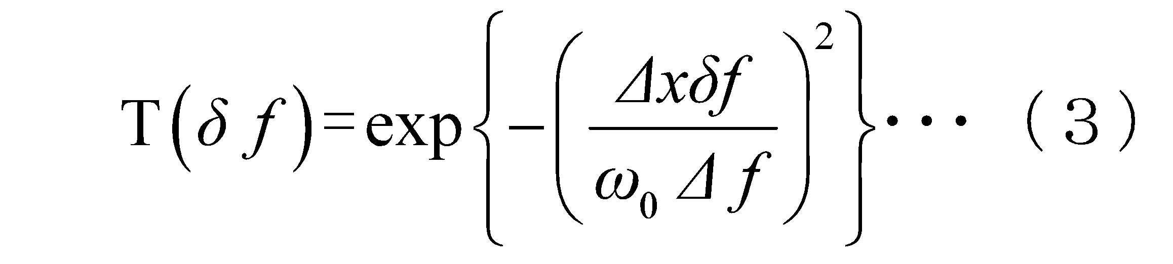
式(3)において、δfは透過中心周波数からの偏差、Δxは第1出力側スラブ導波路105に接続している第1出力導波路107の中心位置の間隔、Δfは隣り合うチャンネル間の中心周波数の間隔、ω0はスポットサイズである。
ここで、δλを透過中心波長からの偏差、Δλを隣り合うチャンネル間の中心波長の間隔とすると以下の(4)式が成り立ち、式(4)を式(3)に代入すると、式(5)が得られる。周波数領域で表されている式(3)が、式(5)により波長領域で表される。
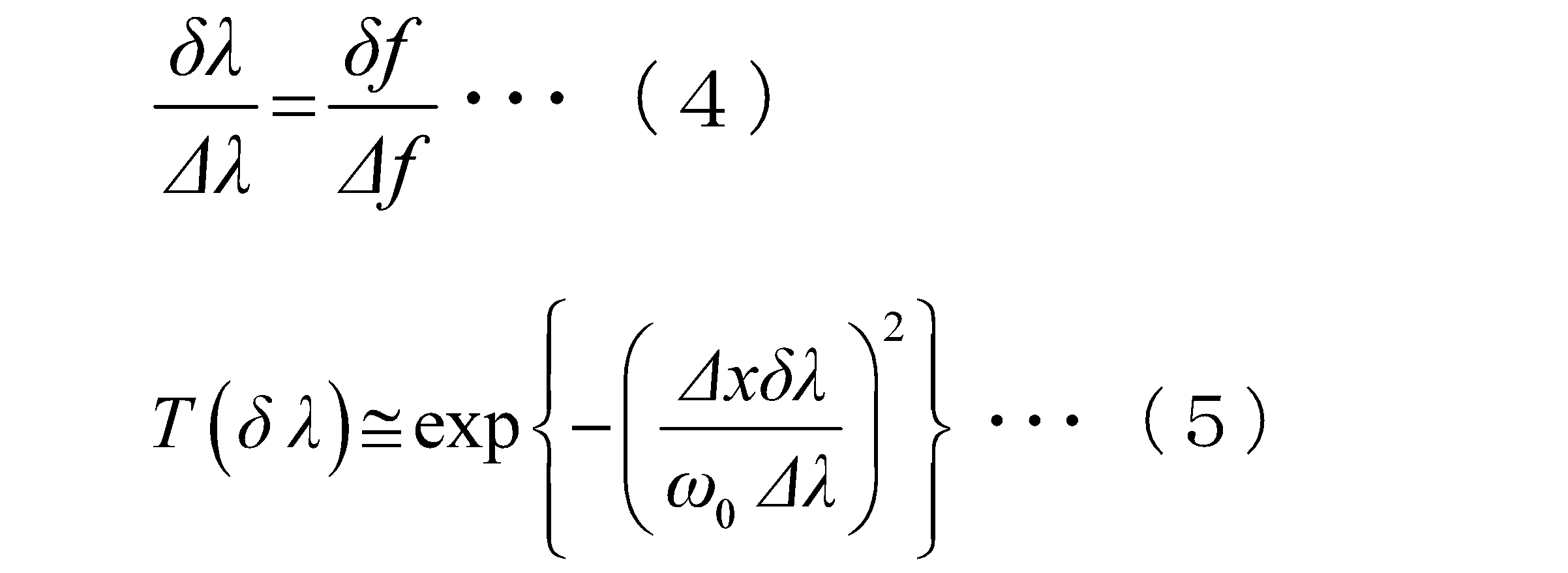
図4は、アレイ導波路回折格子の各チャンネルの透過スペクトルを、式(5)を用いて計算した結果を示している。なお、ガウス関数の急峻さを表すパラメータΔx/ω0は、アレイ導波路回折格子の設計時に調整することができ、このパラメータΔx/ω0は、実施の形態では4.5としている。
ところで、1250nm~1650nmと波長領域が広いので、導波路を構成する石英ガラス中のOH基の吸収により、1380nm近傍の損失などがこの設計のアレイ導波路回折格子にはある。しかしながら、この波長帯は伝送に用いていないので、このアレイ導波路回折格子の動作特性に影響はない。図4に示す計算結果は、導波路を構成する石英ガラス中のOH基の吸収に関する計算を考慮していない。
また、上述したアレイ導波路回折格子は、チャンネル間隔が50nmあるが、石英系導波路を用いた干渉型のフィルタの分波波長の温度依存性は、0.01nm/℃である。屋内・屋外での使用環境温度変化が-5℃から35℃の40℃としても、上述した温度依存性より波長変動は約0.4nmに相当し、隣り合うチャンネル間隔の1/100以下であり、分波特性に影響はない。したがって、上述したアレイ導波路回折格子を実際に使用する際には、ペルチェ素子などを用いて温調をかける必要はない。
また、石英系導波路では、透過スペクトルのTE/TM偏波依存性が0.1~0.2nm程度あるが、本アレイ導波路回折格子は、隣り合うチャンネル間隔=分解能が50nmと大きいので、偏波依存性は無視できる。
[実施の形態2]
次に、本発明の実施の形態2に係る波長チェッカーについて、図5A,図5B,図5Cを参照して説明する。
次に、本発明の実施の形態2に係る波長チェッカーについて、図5A,図5B,図5Cを参照して説明する。
この波長チェッカーは、光導波路チップ101を備える。光導波路チップ101は、前述した実施の形態1と同様である。また、この波長チェッカーは、光導波路チップ101に並んで配置され、出射光を導波する光導波路を備える光導波路チップ121を備える。光導波路チップ121には、複数の直線光導波路が形成されている。例えば、光導波路チップ101の8本の出力導波路に対応し、光導波路チップ121には、8本の直線光導波路が形成されている。また、光導波路チップ101の8本の出力導波路の出力端の間隔と同じ1mm間隔で、8本の直線光導波路が配列されている。
実施の形態2において、光変換部102の出射光が照射される面は、出射光が外部に出力される光導波路チップ121の出力端に向かい合って配置されている。光変換部102は、前述した実施の形態1と同様である。また、光導波路チップ121は、導波方向に光導波路チップ101に直列に並んで配置されている。
また、実施の形態2では、光導波路チップ101、光導波路チップ121は、光導波路チップ141の上に搭載されている。つまり、2層に積層されている。下の光導波路チップを親光導波路チップ、上の光導波路チップを子光導波路チップと定義する。従って、以下では、子光導波路チップ101、子光導波路チップ121、親光導波路チップ141と呼んでいく。親光導波路チップ141は、平面光波回路が形成されていても、光回路が何もなくても(Si基板の上はクラッドガラスのみである)よい。子光導波路チップ101、光導波路チップ121は、各々の光導波路(平面光波回路)が形成されている面(クラッドガラスのある方の面)を、親光導波路チップ141(のクラッドガラスのある面)に向け、図示しないスペーサを介して親光導波路チップ141の上に搭載されている。ここで、光を通そうとする光導波路チップは子光導波路チップである。クラッドガラスのある面を表面とすると、子導波路チップは上から目視するとSi基板のある裏面が見えていることになる。つまり、子光導波路チップにおいて、コアとクラッドで構成される光回路の部分が下側に来るようになっている。また、親光導波路チップ141は、主基板151の上に搭載されている。例えば、親光導波路チップ141は、主基板151の上に接着剤で接着されて固定されている。また、子光導波路チップ101、子光導波路チップ121は、光の入力方向に沿って縦列に並んで配置されている。
また、光変換部102は、主基板151の上に固定された支持部109に支持されている。例えば、子光導波路チップ121の出力端の面に向かい合う支持部109の側面に、赤外光を可視光に変換する変換材料を塗布することで、光変換部102が形成できる。
なお、子光導波路チップ101の入力導波路端には、ファイバーブロック161が接続されている。ファイバーブロック161には、確認対象の光信号を入力するためのコネクター163が設けられた光ファイバー162が接続している。なお、ファイバーブロック161と子光導波路チップ101の入力導波路との調芯には、別途、コネクター付光ファイバー(不図示)が用いられる。また、子光導波路チップ101は、図示しないスペーサを介して親光導波路チップ141に接着剤で接着されて固定されている。一方、子光導波路チップ121は、半固定の状態で、親光導波路チップ141から着脱可能とされ、入れ替え可能とされている。
ここで、親光導波路チップ141の上における子光導波路チップ101、子光導波路チップ121の位置決めについて、図6A,図6Bを参照して説明する。まず、親光導波路チップ141には、複数の第1溝131が形成され、子光導波路チップ101および子光導波路チップ121の各々は、第2溝132が形成されている。また、複数の第1溝131の各々は、一部が親光導波路チップ141から突出した形で複数のスペーサ部材171が嵌合している。また、子光導波路チップ101の第2溝132および子光導波路チップ121の第2溝132の各々も、いずれかの複数のスペーサ部材171の突出した部分と嵌合している。なお、第2溝132の位置は、子光導波路チップ101および子光導波路チップ121の導波路部分(コア)部分を避けて配置されている。溝の数は通常、3個以上あればよい。
第1溝131は、親光導波路チップ141のクラッド層143に形成される。第1溝131は、クラッド層143を貫通し、基板142に到達して形成される。同様に、第2溝132は、子光導波路チップ121のコア123を備えるクラッド層124に形成される。第2溝132は、クラッド層124を貫通し、基板122に到達して形成される。
第1溝131および第2溝132は、公知フォトリソグラフィ技術およびエッチング技術(反応性イオンエッチングなど)により形成できる。フォトリソグラフィ技術で形成したマスクパターンをマスクとし、基板142をエッチング停止層としてクラッド層143をエッチングすることで、第1溝131を形成する。同様に、フォトリソグラフィ技術で形成したマスクパターンをマスクとし、基板122をエッチング停止層としてクラッド層124をエッチングすることで、第2溝132を形成する。
このように形成される、第1溝131および第2溝132の設計に対する面方向の位置の精度(ずれ量)は、マスクパターンの位置精度、およびエッチング時の位置のずれ量で決定される。よく知られているように、マスクパターンの位置精度は、サブミクロン以下であり、反応性イオンエッチングにおける位置ずれもサブミクロン以下である。したがって、第1溝131および第2溝132が形成される面方向の位置は、設計に対して1μm以下となる。
また、第1溝131の深さは、クラッド層143の厚さで決定され、第2溝132の深さは、クラッド層124の厚さで決定される。クラッド層143の厚さの精度、クラッド層124の厚さの精度は、例えば、よく知られたガラス堆積技術により、サブミクロンオーダで定まる。また、クラッド層124に埋め込まれるコア123の厚さ方向の位置も同様である。
ここで、スペーサ部材171は、例えば、光ファイバーを所定の長さに切断することで形成可能であり、各々のスペーサ部材171の直径の精度は、サブミクロンオーダで決定することができる。したがって、子光導波路チップ121の厚さ方向の位置精度も、1μm以内で定まる。
以上のことより、親光導波路チップ141の上に搭載されている子光導波路チップ101と、子光導波路チップ121とは、対応する光導波路のコア中心同士の位置を、正確に一致させることができる。なお、一般に、上述したような親光チップの上に搭載する複数の子チップ間の位置合わせは、各チップに反りが生じていない条件で行っている。なお、より詳しい説明は、特許文献2、非特許文献4、非特許文献5を参照されたい。この光学実装形態は、PPCP(Pluggable Photonic Circuit Platform)と呼ばれている。PPCPにより実装される子光導波路チップ121は、着脱可能であるという特徴がある。このため、様々な機能の子光導波路チップ121を入れ替えて用いることができ、柔軟に様々な機能を持たせることができる。いわば、PPCPは、電子ブロックの光回路(光チップ)版のような特徴を持つとも言える。
次に、子光導波路チップ121の製造について、図7A~図7Eを参照して説明する。
まず、図7Aに示すように、Siからなる基板122を用意する。次に、図7Bに示すように、基板122の上に、下部クラッド層124aを形成し、下部クラッド層124aの上に、コア形成層301を形成する。
例えば、火炎堆積(FHD)法により、下部クラッド層124a,コア形成層301が形成できる。まず、酸水素炎中に、原料ガス(主成分:四塩化シリコン)を通し、加熱加水分解したガラス微粒子を基板122の上に堆積させ、下部クラッド層124aとなる第1の微粒子層を形成する。引き続き、原料ガスの組成を変更する(GeO2ドーパント濃度を変える)ことで組成の異なるガラス微粒子を第1の微粒子層の上に堆積させ、コア形成層301となる第2の微粒子層を形成する。この後、例えば、電気炉などを用いて、第1の微粒子層および第2の微粒子層を加熱することで、各々を透明なガラス組成の膜とすることで、下部クラッド層124a,コア形成層301とする。なお、これらの層は、化学的気相成長法により形成することもできる。
次に、半導体装置の製造に用いられる公知のリソグラフィー技術およびエッチング技術によりコア形成層301をパターニングすることで、図7Cに示すように、コア123を形成する。例えば、フォトリソグラフィ技術により、コア123とする部分の上にレジストパターンをコア形成層301の上に形成する。次に、形成したレジストパターンをマスクとし、反応性イオンエッチング(RIE)によりコア形成層301をエッチングし、コア123となる部分を残して他のコア形成層を除去する。この後、レジストパターンを除去すれば、コア123が形成できる。
次に、図7Dに示すように、コア123の上に上部クラッド層124bを形成する。前述した下部クラッド層124aと同様に、FHD法により、上部クラッド層124bが形成できる。
次に、公知のリソグラフィー技術およびエッチング技術により上部クラッド層124bおよび下部クラッド層124aをパターニングすることで、図7Eに示すように、上部クラッド層124bおよび下部クラッド層124aを貫通して基板122に到達する第2溝132を形成する。例えば、フォトリソグラフィ技術により、第2溝132を形成する箇所に開口を有するレジストパターンを、上部クラッド層124bの上に形成する。次に、形成したレジストパターンをマスクとし、RIEにより上部クラッド層124bおよび下部クラッド層124aをエッチングし、第2溝132となる部分を除去する。この後、レジストパターンを除去すれば、第2溝132が形成できる。
図8に、子光導波路チップ121の出射部を拡大した断面を示す。例えば、光導波路中をモードフィールド径(MFD:Mode Field Diameter)6μm(=スポットサイズ3μm)で光が導波しているとする。このモードフィールド径は、例えばコアの断面の寸法4.5μm×4.5μm(矩形)、コアとクラッドとの間の比屈折率差1.5%の光導波路で実現されるモードフィールド径がおおよそ対応する。なお、スポットサイズはMFDの半分である。
MFD6μmの光が端面から出射されるとビームは回折により広がる。以下、光導波路中の電界分布をガウス分布であると近似してビームの広がりを計算する。出射端のスポットサイズをω0とすると、出射端面から距離zだけ伝搬した先でのビーム径は式(6)で表される。これは非特許文献6に詳しく述べられている。式(6)において、λは波長である。式(6)の√の中の2乗項が1より十分大きくなる条件(この場合z>100μm程度)で、式(6)は式(7)で近似できる。
式(7)をプロットしたものが図9である。z=1mmぐらいからが考察する領域であり、正確な値が得られることがわかる。図9から、距離3.5mm程度伝搬するとスポットサイズが500mμmになり、MFDは1mmと光導波路ピッチと同じになる(スポットサイズは、MFDの半分である)。この距離より光変換部102(支持部109)を、子光導波路チップ121の出射端から離すと、隣接チャンネルからの出射光(の可視光変換光)と区別がつけられづらくなることがわかる。
ここで、子光導波路チップ121の上部クラッド層124bが薄い(30μm以下)ことと、親光導波路チップ141のクラッド層143が薄い(~50μm)ことから、子光導波路チップ121の出射側の端面が、親光導波路チップ141の光変換部102側の端面より光変換部102から離れていると、子光導波路チップ121の出射光が、親光導波路チップ141の、クラッド層143や基板142の部分に入り屈折するこし、光変換部102に照射されるビームの形状が変形して認識しづらくなる。空気の屈折率が1に対し、クラッドを億制する石英系ガラスの屈折率は1.4~1.5であり、基板を構成するSiの屈折率は3.5と差がさらに大きいので屈折角もさらに大きくなる。
このため,子光導波路チップ121の出射側(光変換部102の側)の端面は、親光導波路チップ141の光変換部102側の端面と光変換部102の側に同一の位置とされている、または、親光導波路チップ141の光変換部102の側の端面より光変換部102の側に配置されていることが重要となる。
なお、図5A,図5B,図5Cを用いて説明した実施の形態2に係る波長チェッカーにおいても、子光導波路チップ121の透過スペクトルは、実施の形態1と同様であり、図4に示されるスペクトルが得られる。
ところで、図10に示すように、アレイ導波路回折格子を備える子光導波路チップ121aを子光導波路チップ121と入れ替えて用いることも可能である。子光導波路チップ121aは、分波波長間隔が狭いアレイ導波路回折格子を備える。図10において、符号125は、第2アレイ導波路、符号126は、第2入力側スラブ導波路、符号127は、第2出力側スラブ導波路、符号128は、第2入力導波路、符号129は、第2出力導波路をそれぞれ示している。これは、第2アレイ導波路125が、平面視で円弧の形をしている通常のアレイ導波路回折格子である。分波波長が1550nmから1600nm、分波波長間隔が5nm間隔、10ポートのアレイ導波路回折格子である。なお、図10では、一部の第2出力導波路129を省略して示している。
図11に、子光導波路チップ101と子光導波路チップ121aとの接続状態を示す。図11に示すように、子光導波路チップ101の第1出力導波路107のポート7に、子光導波路チップ121aの第2入力導波路128を光学的に接続する場合を検討する。この場合における、子光導波路チップ121の(分波波長間隔が狭い)アレイ導波路回折格子の透過波長スペクトルを図12に示す。このスペクトルは、式(5)を用いて計算した結果である。一方、子光導波路チップ101のアレイ導波路回折格子の透過スペクトルは、図13に示すようなブロードなスペクトルになる。子光導波路チップ101と子光導波路チップ121aとを接続した構成における透過スペクトルは図12に示すスペクトルと図13に示すスペクトルの合成となるので、図14に示すようなスペクトルになる。
子光導波路チップ101に、直線光導波路から構成した子光導波路チップ121を組み合わせた場合の透過スペクトルは図4に示すものとなり、波長分解能が50nmである。これに対し、子光導波路チップ101に、アレイ導波路回折格子から構成した子光導波路チップ121aを組み合わせた場合の透過スペクトルでは、波長分解能は5nmになり、より高精細に波長を確認できることがわかる。
また、子光導波路チップ101に子光導波路チップ121を組み合わせた構成では、図4に示すように属艇レンジが1250nm~1650nmの400nmと広帯域となる。これに対し、子光導波路チップ101に子光導波路チップ121aを組み合わせた構成では、図14に示すように狭帯域となる。
これらのように、PPCP実装により子光導波路チップ121と子光導波路チップ121aとを交換可能にすることで、波長チェッカーの波長分解能・測定レンジを柔軟に変更することができるようになる。
なお、上述した説明では、波長1550nmから1600nmの波長領域に関して、狭い波長間隔のアレイ導波路回折格子を用いてより高精細に波長を確認しているが、子光導波路チップ101のアレイ導波路回折格子の別の出力ポートに、ここより出力される波長範囲対応した5nm間隔10ポートのアレイ導波路回折格子を用意して接続すれば、他の波長範囲でも5nmの波長分解能で波長を確認できることがわかる。
ここで、分波波長間隔が狭いアレイ導波路回折格子について説明を追加する。フリースペクトラルレンジ(FSR)が、チャンネル間隔×チャンネル数に等しいものをサイクリックアレイ導波路回折格子(周回性アレイ導波路回折格子)と呼ぶ。狭い波長間隔のアレイ導波路回折格子に、上記の周回性アレイ導波路回折格子を用いれば、子光導波路チップ101に接続する光チップを、同じ周回性アレイ導波路回折格子で共用することができる。ただし、1500nm帯と1300nm帯といったようなあまりに波長が離れているチャンネルでは、屈折率分散の影響で、屈折率差が大きくなってくるので、アレイ導波路回折格子の共用はできない。
上述では、波長チェッカーのデバイス構造について説明したが、ここで、波長検査方法の観点から若干補足する。アクセス系PONシステムの波長検査方法としても、波長をアレイ導波路回折格子で波長ごとに分波して、近赤外光を可視光に変換する材料(波長変換材料)に照射して、光ったポートから波長を目視で確認する検査方法も提案することができる。アレイ導波路回折格子の広義の解釈は、回折格子(グレーティング)であるので、波長を回折格子(グレーティング)で波長ごとに分光して波長変換材料に照射して、光った位置から波長を目視で確認する検査方法も提案することができる。これ等の検査方法は、電源等を用いずに簡易に波長検査ができるという特徴を有している。
[実施の形態3]
次に、本発明の実施の形態3に係る波長チェッカーについて、図15を参照して説明する。実施の形態3では、図5A,図5B,図5Cを用いて説明した波長チェッカーにおいて、子光導波路チップ101の代わりに、図15に示す子光導波路チップ101aを用いる。子光導波路チップ101aは、主第1入力導波路106a,副第1入力導波路106bが、第1入力側スラブ導波路104の入力側に接続されている。他の構成は、子光導波路チップ101と同様である。
次に、本発明の実施の形態3に係る波長チェッカーについて、図15を参照して説明する。実施の形態3では、図5A,図5B,図5Cを用いて説明した波長チェッカーにおいて、子光導波路チップ101の代わりに、図15に示す子光導波路チップ101aを用いる。子光導波路チップ101aは、主第1入力導波路106a,副第1入力導波路106bが、第1入力側スラブ導波路104の入力側に接続されている。他の構成は、子光導波路チップ101と同様である。
ここで、複数の第1出力導波路107の第1出力側スラブ導波路105との接続部分における導波路間隔をΔxoutとすると、主第1入力導波路106aの第1入力側スラブ導波路104との接続部分と、副第1入力導波路106bの第1入力側スラブ導波路104との接続部分との間の導波路間隔は,Δxout/2とされている。また、子光導波路チップ101aにおいて、第1入力側スラブ導波路104と第1アレイ導波路103と第1出力側スラブ導波路105とは、平面視の形状が、第1入力側スラブ導波路104の中心と第1出力側スラブ導波路105の中心とを結ぶ線分の中点を通り線分に垂直な直線を中心に線対称とされている。第1入力側スラブ導波路104は、入力導波路に接している側とアレイ導波路に接している側とは同じ曲率の円弧になっている。従って、入力側スラブ導波路の中心はスラブ導波路の外形を構成している直線と円弧が交わる4つの点を対角に結んだ直線の交点となる。第1出力側スラブ導波路105においても同様である。
以下、より詳細に説明する。
主第1入力導波路106aを第1入力側スラブ導波路104の中心に接続する。また第1出力側スラブ導波路105の中心に対し、各々の第1出力導波路107を導波路間隔Δxoutで接続し、第1出力導波路107の各々に対して透過中心波長がλ1、λ2、λ3、・・・λ8と等波長間隔で分岐されているものとする。また、副第1入力導波路106bは、主第1入力導波路106aに対して導波路間隔Δx=Δxoutで第1入力側スラブ導波路104に接続する(図16A,図16B参照)。
前述したように、第1入力側スラブ導波路104、第1アレイ導波路103、第1出力側スラブ導波路105の平面視の形状が線対称とされていれば(非特許文献2参照)、以下のことが成立する。
主第1入力導波路106aに対して副第1入力導波路106bをずらして接続すると、副第1入力導波路106bに入力される波長多重光は、第1出力導波路107の各々に対し、透過中心波長が、λ2、λ3、λ4、・・・λ9と、等間隔に分岐される。これは、副第1入力導波路106bが1個分ずれたので、第1アレイ導波路103に達するときの波面が傾き、この結果、第1出力導波路107に到達した際の波面が傾き、同じ波長は、1個分だけずれた第1出力導波路107に集光されることになるからである。
主第1入力導波路106aと副第1入力導波路106bとの導波路間隔Δx=Δxout/2とすると、隣り合うチャンネル間の中心波長間隔をΔλとして、透過中心波長がλ1+Δλ/2、λ2+Δλ/2、λ3+Δλ/2、・・・λ8+Δλ/2となる。なお、Δλ=λ2-λ1=λ3-λ2=・・・=λ9-λ8である。
子光導波路チップ101aにおけるアレイ導波路回折格子の設計を子光導波路チップ101と同様にすると、主第1入力導波路106aから入力されてアレイ導波路回折格子を透過するスペクトル(計算値)は,図17Aに示すように、子光導波路チップ101の透過スペクトルと同じスペクトルになる。つまり、第1出力導波路107の各々の透過中心波長は、1275nm、1325nm、1375nm、1425nm、1475nm、1525nm、1575nm、1625nmとなる。
一方、副第1入力導波路106bから入力されてアレイ導波路回折格子を透過するスペクトル(計算値)は、図17Bに示すように、波長間隔の半分だけずれて、1300nm、1350nm、1400nm、1450nm、1500nm、1550nm、1600nm、1650nmとなる。つまり、主第1入力導波路106aからの透過スペクトルと、副第1入力導波路106bからのスペクトルとは互い違いになる。
アレイ導波路回折格子への入力導波路が1本ある場合に比べて、主第1入力導波路106a,副第1入力導波路106bがある効果は、以下の通りである。入力導波路が1本の場合、隣り合う第1出力導波路107の透過スペクトル間の波長の光が入力された場合に、透過率が低くなっているために、近赤外光から可視光に変換された光も弱くなっており、光変換部102における発光が認識できない場合がある。
例えば、図17Aの波長1300nmにおけるポート1、ポート2における透過光強度は、最も透過する波長(波長1275nmや1325nm)に比較して20dBも劣化してしまう。
これに対し、主第1入力導波路106a,副第1入力導波路106bを用いる場合、副第1入力導波路106bにも信号光を入力することにより、波長1300nmにおけるポート1の透過光強度は、最も透過する波長となる。この結果、主第1入力導波路106a,副第1入力導波路106bを用いることにより、図17Aと図17Bを重ね合わせた図18に示すように、最も透過しない波長でも最大透過波長に比較して5dB劣化で済むことがわかる(波長1250nm周辺を除く)。
したがって、入力導波路を1本として信号光を入れても、信号光に対する透過光強度が弱いため波長がわからない場合も、主第1入力導波路106a,副第1入力導波路106bを用いて両者に信号光を入れることで、光変換部102におけるより強い発光が得られ、より確実な波長の認識が可能となる。
[実施の形態4]
次に、本発明の実施の形態4に係る波長チェッカにーついて、図19を参照して説明する。実施の形態4では、図5A,図5B,図5Cを用いて説明した波長チェッカーにおいて、子光導波路チップ101の代わりに、図15に示す子光導波路チップ101aを用い、直線光導波路からなる子光導波路チップ121の代わりに、分波波長間隔が狭いアレイ導波路回折格子を備える子光導波路チップ121aを用いる。子光導波路チップ121aのアレイ導波路回折格子は、分波波長が1550nmから1600nm、分波波長間隔が5nm間隔、10ポートのアレイ導波路回折格子である。
次に、本発明の実施の形態4に係る波長チェッカにーついて、図19を参照して説明する。実施の形態4では、図5A,図5B,図5Cを用いて説明した波長チェッカーにおいて、子光導波路チップ101の代わりに、図15に示す子光導波路チップ101aを用い、直線光導波路からなる子光導波路チップ121の代わりに、分波波長間隔が狭いアレイ導波路回折格子を備える子光導波路チップ121aを用いる。子光導波路チップ121aのアレイ導波路回折格子は、分波波長が1550nmから1600nm、分波波長間隔が5nm間隔、10ポートのアレイ導波路回折格子である。
まず、図19に示すように、子光導波路チップ101aのアレイ導波路回折格子には、主第1入力導波路106aから光を入れることを考え、子光導波路チップ101aの第1出力導波路107のなかでポート7に、子光導波路チップ121aの第2入力導波路128が接続している構成を考える。子光導波路チップ121aのアレイ導波路回折格子の透過波長スペクトルは図12に示すものとなり、前述の説明と同様に、子光導波路チップ101a+子光導波路チップ121aの透過スペクトルは図20のようなスペクトルになる。
次に、子光導波路チップ101aのアレイ導波路回折格子には、副第1入力導波路106bから光を入れることを考え、子光導波路チップ101aの第1出力導波路107のなかでポート7に、子光導波路チップ121aの第2入力導波路128が接続している構成を考える。子光導波路チップ101aのポート7の透過スペクトルは図21のようになる。図21に示すスペクトルは、主第1入力導波路106aから光を入れた場合の透過スペクトル(図13)より、半波長間隔(25nm)ほど長波にシフトしていることがわかる。一方、子光導波路チップ121aの透過スペクトルは、図12で表されるので、子光導波路チップ101aと子光導波路チップ121aとを透過するスペクトルは図22のように表される。
次に、子光導波路チップ101aのアレイ導波路回折格子には、副第1入力導波路106bから光を入れることを考え、子光導波路チップ101aの第1出力導波路107のなかでポート6に、子光導波路チップ121aの第2入力導波路128が接続している構成を考える。子光導波路チップ101aのポート6の透過スペクトルは図23のように表される。図23に示すスペクトルは、図13に示すスペクトルより波長間隔分短波にシフトしている。一方、子光導波路チップ121aの透過スペクトルは、図12で表されるので、子光導波路チップ101aと子光導波路チップ121aとを透過するスペクトルは図24のように表される。
以上に説明したことより、子光導波路チップ101aの主第1入力導波路106aと副第1入力導波路106bとを用いた透過スペクトルは、図20のスペクトル、図22のスペクトル、図24のスペクトルを合成した図25に示すスペクトルとなる。
子光導波路チップ101+子光導波路チップ121aの透過スペクトルは、図14に示すものとなり、波長1570nm~1580nmでは、高い透過率を示すが、1550、1600nm近傍は透過率が低くなり、信号光が認識できない可能性がある。これに対し、子光導波路チップ101a+子光導波路チップ121a場合、合成透過スペクトルは図25のようになり、1550nm、1600nm近傍でも透過率は高まり、信号光を認識できる波長範囲を広げることができるようになる。
なお、上述では、2つの主第1入力導波路106a,副第1入力導波路106bを備える子光導波路チップ101aを用いることで、透過率が高い波長領域を広げたが、子光導波路チップ121aのアレイ導波路回折格子においても、入力導波路を2つにすることで、透過率が高い波長領域をさらに広げることが可能である。
[実施の形態5]
次に、本発明の実施の形態5に係る波長チェッカーについて、図26を参照して説明する。図11を用いて説明した波長チェッカーの子光導波路チップ121aの代わりに、図26に示すように、直線光導波路からなる光導波路部120aと、分波波長間隔が狭いアレイ導波路回折格子120bとを備える子光導波路チップ121bを用いる。
次に、本発明の実施の形態5に係る波長チェッカーについて、図26を参照して説明する。図11を用いて説明した波長チェッカーの子光導波路チップ121aの代わりに、図26に示すように、直線光導波路からなる光導波路部120aと、分波波長間隔が狭いアレイ導波路回折格子120bとを備える子光導波路チップ121bを用いる。
子光導波路チップ101および子光導波路チップ121bを搭載する親光チップに、子光導波路チップ121bとの嵌合のための溝を余分に設け、子光導波路チップ121bを、光導波方向に垂直な方向に移動可能とする。このようにすることで、子光導波路チップ121bを親光チップの上でスライドさせ、子光導波路チップ121bを移動することで、子光導波路チップ101と光導波路部120aとの接続、および子光導波路チップ101とアレイ導波路回折格子120bとの接続とを切替可能とする。
前述したPPCPによる実装形態では、子光導波路チップ121と子光導波路チップ121aとを個別に用意する必要があったが、実施の形態5によれば、1個の子光導波路チップ121bを用意すればよくなり、部品点数を削減する効果がある。一般に、子光導波路チップ121aのアレイ導波路回折格子は、波長帯域が異なると別個のアレイ導波路回折格子を用意する必要があるが、実施の形態5によれば、例えば、検査分解能を高くする波長領域に必要なアレイ導波路回折格子を、子光導波路チップ121bにチップスペースが許す範囲で入れ込めればよい。
以上に説明したように、本発明によれば、赤外光を可視光に変換する変換材料から構成された光変換部を、光導波路チップの複数の第1出力導波路の出力側におくことで、複数の第1出力導波路より出射される出射光を受光可能に配置したので、PONシステムの開通、故障切り分けなどにおける信号光の有無の確認などが、容易に実施できるようになる。
なお、本発明は以上に説明した実施の形態に限定されるものではなく、本発明の技術的思想内で、当分野において通常の知識を有する者により、多くの変形および組み合わせが実施可能であることは明白である。
101…アレイ導波路チップ、102…光変換部、103…第1アレイ導波路、103a…コア部、104…第1入力側スラブ導波路、104a…コア部、105…第1出力側スラブ導波路、106…第1入力導波路、106a…主入力導波路、106b…副入力導波路、107…第1出力導波路、108…出力端、111…基板、112…下部クラッド層、113…上部クラッド層、120a…光導波路部、120b…アレイ導波路回折格子、121…光導波路チップ、121a…子光導波路チップ、121b…子光導波路チップ、122…基板、123…コア、124…クラッド層、124a…下部クラッド層、124b…上部クラッド層、125…第2アレイ導波路、126…第2入力側スラブ導波路、127…第2出力側スラブ導波路、128…第2入力導波路、129…第2出力導波路、131…第1溝、132…第2溝、141…光導波路チップ、142…基板、143…クラッド層、151…主基板、161…ファイバーブロック、162…光ファイバー、163…コネクター、171…スペーサ部材、501…アレイ導波路、502…入力側スラブ導波路、503…出力側スラブ導波路、504…入力導波路、505…出力導波路。
Claims (8)
- 光導波路チップと近赤外光を可視光に変換する変換材料から構成された光変換部を備える波長チェッカーにおいて、
光ファイバーと接続している側の前記光導波路チップがアレイ導波路回折格子を含み、かつ主基板の上に搭載されており、
前記主基板上に支持部が固定されており、
前記支持部は外部空間に光を出力する側の前記光導波路チップの光出射端面と対向する位置にあり、前記光変換部は前記光出射端面に面している前記支持部の側面に備えられる
ことを特徴とする波長チェッカー。 - 請求項1記載の波長チェッカーにおいて、
前記光導波路チップは2層に積層され、
前記光導波路チップが基板及び基板上のコアとクラッドもしくは基板及び基板上のクラッドから構成され、
前記クラッド側を前記光導波路チップの表面と定義すると、
積層されている上下層の前記光導波路チップの表面を対向させ、
下層側の前記光導波路チップを親光導波路チップ、上層側の前記光導波路チップを子光導波路チップと定義すると、前記親光導波路チップが1個あり、前記子光導波路チップが複数あり、
前記親光導波路チップのクラッド部分に複数の第1溝が形成され、前記子光導波路チップのクラッド部分に複数の第2溝が形成され、
前記複数の第1溝の各々は、一部が前記親光導波路チップから突出した形で複数のスペーサ部材が嵌合し、
前記子光導波路チップの第2溝の各々は、いずれかの前記複数のスペーサ部材の突出した部分と嵌合し、
光ファイバーと接続している側の前記子光導波路チップは、アレイ導波路回折格子を含み、他の前記子光導波路チップは直線導波路群もしくはアレイ導波路回折格子の少なくとも一方を含み、
前記親光導波路チップは主基板上に固定されている
ことを特徴とする波長チェッカー。 - 請求項2記載の波長チェッカーにおいて、
前記スペーサ部材は、光ファイバーから構成されていることを特徴とする波長チェッカー。 - 請求項1~3のいずれか1項に記載の波長チェッカーにおいて、
前記光導波路チップの前記基板がSi基板であり、前記コアと前記クラッドが石英系ガラスで構成されている
ことを特徴とする波長チェッカー。 - 請求項1~4のいずれか1項に記載の波長チェッカーにおいて、
前記子光導波路チップチップの前記光変換部の側の端面は、前記親光導波路チップの前記光変換部の側の端面と同一の位置とされている、または、前記親光導波路チップの前記光変換部の側の端面より前記光変換部の側に配置されていることを特徴とする波長チェッカー。 - 請求項1~5のいずれか1項に記載の波長チェッカーにおいて、
前記子光導波路チップは、光の入力方向に沿って縦列に並んで配置されていることを特徴とする波長チェッカー。 - 請求項1~6のいずれか1項に記載の波長チェッカーにおいて、
前記光ファイバーに接続している側の前記子光導波路チップに含まれる前記アレイ導波路回折格子において、
前記アレイ導波路回折格子が入力導波路、入力側スラブ導波路、複数のアレイ導波路、出力側スラブ導波路、複数の出力側導波路から構成され、
前記入力側スラブ導波路と前記複数のアレイ導波路と前記出力側スラブ導波路は、平面視の形状が、前記入力側スラブ導波路と出力側スラブ導波路の中心とを結ぶ線分の中点を通りこの線分に垂直な直線を中心に線対称となるように形成され、
前記入力導波路が、主入力導波路と副入力導波路からなり、
前記出力側スラブ導波路に前記複数の出力導波路が接続する部分の接続間隔をΔxoutとすると、前記主入力導波路と前記副入力導波路が前記入力側スラブ導波路に接続する部分の接続間隔がΔxout/2である
ことを特徴とする波長チェッカー。 - 請求項1~7のいずれか1項に記載の波長チェッカーにおいて、
前記変換材料はフォスファーであることを特徴とする波長チェッカー。
Priority Applications (1)
| Application Number | Priority Date | Filing Date | Title |
|---|---|---|---|
| US17/285,209 US11693179B2 (en) | 2018-11-22 | 2019-11-08 | Wavelength checker |
Applications Claiming Priority (2)
| Application Number | Priority Date | Filing Date | Title |
|---|---|---|---|
| JP2018-219011 | 2018-11-22 | ||
| JP2018219011A JP7099279B2 (ja) | 2018-11-22 | 2018-11-22 | 波長チェッカー |
Publications (1)
| Publication Number | Publication Date |
|---|---|
| WO2020105472A1 true WO2020105472A1 (ja) | 2020-05-28 |
Family
ID=70774498
Family Applications (1)
| Application Number | Title | Priority Date | Filing Date |
|---|---|---|---|
| PCT/JP2019/043838 Ceased WO2020105472A1 (ja) | 2018-11-22 | 2019-11-08 | 波長チェッカー |
Country Status (3)
| Country | Link |
|---|---|
| US (1) | US11693179B2 (ja) |
| JP (1) | JP7099279B2 (ja) |
| WO (1) | WO2020105472A1 (ja) |
Families Citing this family (2)
| Publication number | Priority date | Publication date | Assignee | Title |
|---|---|---|---|---|
| US11747557B2 (en) * | 2019-08-23 | 2023-09-05 | Nippon Telegraph And Telephone Corporation | Wavelength checker |
| JP2022038756A (ja) * | 2020-08-27 | 2022-03-10 | 富士通株式会社 | 光導波路 |
Citations (4)
| Publication number | Priority date | Publication date | Assignee | Title |
|---|---|---|---|---|
| JP2003218813A (ja) * | 2002-01-22 | 2003-07-31 | Sankosha Corp | 光信号監視装置 |
| US20090016716A1 (en) * | 2007-07-12 | 2009-01-15 | Aidi Corporation | Fiber array unit with integrated optical power monitor |
| JP2012093450A (ja) * | 2010-10-25 | 2012-05-17 | Panasonic Corp | 光モジュール |
| JP2017194565A (ja) * | 2016-04-20 | 2017-10-26 | 日本オクラロ株式会社 | 光通信モジュール及びその製造方法 |
Family Cites Families (6)
| Publication number | Priority date | Publication date | Assignee | Title |
|---|---|---|---|---|
| JP2706585B2 (ja) * | 1991-09-25 | 1998-01-28 | 日本電信電話株式会社 | 光ファイバ断線検知器及び検知方法 |
| JPH08136404A (ja) * | 1994-11-07 | 1996-05-31 | Sony Corp | 光ファイバケーブル端面判定装置およびその方法 |
| JP3222810B2 (ja) | 1996-08-06 | 2001-10-29 | 日本電信電話株式会社 | アレイ導波路格子 |
| JP2003294961A (ja) * | 2002-04-03 | 2003-10-15 | Sumitomo Electric Ind Ltd | 光通信器検査装置 |
| US7110627B2 (en) | 2002-10-24 | 2006-09-19 | Applied Research & Photonics, Inc. | Reflective arrayed waveguide grating |
| JP6175106B2 (ja) | 2015-08-06 | 2017-08-02 | 日本電信電話株式会社 | 光信号処理装置 |
-
2018
- 2018-11-22 JP JP2018219011A patent/JP7099279B2/ja active Active
-
2019
- 2019-11-08 WO PCT/JP2019/043838 patent/WO2020105472A1/ja not_active Ceased
- 2019-11-08 US US17/285,209 patent/US11693179B2/en active Active
Patent Citations (4)
| Publication number | Priority date | Publication date | Assignee | Title |
|---|---|---|---|---|
| JP2003218813A (ja) * | 2002-01-22 | 2003-07-31 | Sankosha Corp | 光信号監視装置 |
| US20090016716A1 (en) * | 2007-07-12 | 2009-01-15 | Aidi Corporation | Fiber array unit with integrated optical power monitor |
| JP2012093450A (ja) * | 2010-10-25 | 2012-05-17 | Panasonic Corp | 光モジュール |
| JP2017194565A (ja) * | 2016-04-20 | 2017-10-26 | 日本オクラロ株式会社 | 光通信モジュール及びその製造方法 |
Also Published As
| Publication number | Publication date |
|---|---|
| JP7099279B2 (ja) | 2022-07-12 |
| US11693179B2 (en) | 2023-07-04 |
| US20210373233A1 (en) | 2021-12-02 |
| JP2020086081A (ja) | 2020-06-04 |
Similar Documents
| Publication | Publication Date | Title |
|---|---|---|
| CN111226147B (zh) | 中阶梯光栅复用器或解复用器 | |
| CN114641720B (zh) | 偏振系统和方法 | |
| US7555175B2 (en) | Arrayed waveguide grating optical multiplexer/demultiplexer | |
| JPH116928A (ja) | アレイ導波路格子型波長合分波器 | |
| JP2004239991A (ja) | 光機能デバイス | |
| KR20030009765A (ko) | 광도파로 소자의 패키징 장치 | |
| JP4385224B2 (ja) | 光導波路デバイス及び光導波路モジュール | |
| US8532494B2 (en) | Optical bidirectional communication module and optical bidirectional communication apparatus | |
| JP2015035553A (ja) | 波長モニタおよび光モジュール | |
| JP2002323626A (ja) | 光波長合分波器および光合分波システム | |
| US11693179B2 (en) | Wavelength checker | |
| JP2001519923A (ja) | 光学スペクトルに含まれるスペクトル光線を多重化解除する装置 | |
| US20020176660A1 (en) | Optical wavelength multiplexer/demultiplexer and use method thereof | |
| Lee et al. | Design and simulation of fabrication-error-tolerant triplexer based on cascaded Mach–Zehnder inteferometers | |
| JP7215595B2 (ja) | 波長チェッカー | |
| US6539158B2 (en) | Optical waveguide circuit | |
| JP7215593B2 (ja) | 波長チェッカー | |
| JP7124638B2 (ja) | 波長チェッカー | |
| KR101501140B1 (ko) | 광 파워 모니터 구조를 개량시킨 평판형 광도파로 소자 모듈 | |
| JP7215584B2 (ja) | 波長チェッカー | |
| US7305185B2 (en) | Device for integrating demultiplexing and optical channel monitoring | |
| US7006727B2 (en) | Combined multiplexer and demultiplexer for optical communication systems | |
| JP4205701B2 (ja) | 広帯域波長合分波フィルタ | |
| CN106199829A (zh) | 一种具有信道监控功能的阵列波导光栅 | |
| Biswas et al. | A Review on Arrayed Waveguide Grating Multiplexer/De-multiplexer forDense Wavelength Division Multiplexing Systems |
Legal Events
| Date | Code | Title | Description |
|---|---|---|---|
| 121 | Ep: the epo has been informed by wipo that ep was designated in this application |
Ref document number: 19888120 Country of ref document: EP Kind code of ref document: A1 |
|
| NENP | Non-entry into the national phase |
Ref country code: DE |
|
| 122 | Ep: pct application non-entry in european phase |
Ref document number: 19888120 Country of ref document: EP Kind code of ref document: A1 |