WO2020105160A1 - 接合基板の製造方法 - Google Patents
接合基板の製造方法Info
- Publication number
- WO2020105160A1 WO2020105160A1 PCT/JP2018/043124 JP2018043124W WO2020105160A1 WO 2020105160 A1 WO2020105160 A1 WO 2020105160A1 JP 2018043124 W JP2018043124 W JP 2018043124W WO 2020105160 A1 WO2020105160 A1 WO 2020105160A1
- Authority
- WO
- WIPO (PCT)
- Prior art keywords
- copper plate
- silicon nitride
- main surface
- bonded
- brazing material
- Prior art date
- Legal status (The legal status is an assumption and is not a legal conclusion. Google has not performed a legal analysis and makes no representation as to the accuracy of the status listed.)
- Ceased
Links
Images

Classifications
-
- B—PERFORMING OPERATIONS; TRANSPORTING
- B23—MACHINE TOOLS; METAL-WORKING NOT OTHERWISE PROVIDED FOR
- B23K—SOLDERING OR UNSOLDERING; WELDING; CLADDING OR PLATING BY SOLDERING OR WELDING; CUTTING BY APPLYING HEAT LOCALLY, e.g. FLAME CUTTING; WORKING BY LASER BEAM
- B23K1/00—Soldering, e.g. brazing, or unsoldering
-
- B—PERFORMING OPERATIONS; TRANSPORTING
- B23—MACHINE TOOLS; METAL-WORKING NOT OTHERWISE PROVIDED FOR
- B23K—SOLDERING OR UNSOLDERING; WELDING; CLADDING OR PLATING BY SOLDERING OR WELDING; CUTTING BY APPLYING HEAT LOCALLY, e.g. FLAME CUTTING; WORKING BY LASER BEAM
- B23K1/00—Soldering, e.g. brazing, or unsoldering
- B23K1/19—Soldering, e.g. brazing, or unsoldering taking account of the properties of the materials to be soldered
-
- C—CHEMISTRY; METALLURGY
- C04—CEMENTS; CONCRETE; ARTIFICIAL STONE; CERAMICS; REFRACTORIES
- C04B—LIME, MAGNESIA; SLAG; CEMENTS; COMPOSITIONS THEREOF, e.g. MORTARS, CONCRETE OR LIKE BUILDING MATERIALS; ARTIFICIAL STONE; CERAMICS; REFRACTORIES; TREATMENT OF NATURAL STONE
- C04B37/00—Joining burned ceramic articles with other burned ceramic articles or other articles by heating
- C04B37/02—Joining burned ceramic articles with other burned ceramic articles or other articles by heating with metallic articles
-
- H—ELECTRICITY
- H10—SEMICONDUCTOR DEVICES; ELECTRIC SOLID-STATE DEVICES NOT OTHERWISE PROVIDED FOR
- H10W—GENERIC PACKAGES, INTERCONNECTIONS, CONNECTORS OR OTHER CONSTRUCTIONAL DETAILS OF DEVICES COVERED BY CLASS H10
- H10W40/00—Arrangements for thermal protection or thermal control
- H10W40/10—Arrangements for heating
-
- H—ELECTRICITY
- H10—SEMICONDUCTOR DEVICES; ELECTRIC SOLID-STATE DEVICES NOT OTHERWISE PROVIDED FOR
- H10W—GENERIC PACKAGES, INTERCONNECTIONS, CONNECTORS OR OTHER CONSTRUCTIONAL DETAILS OF DEVICES COVERED BY CLASS H10
- H10W70/00—Package substrates; Interposers; Redistribution layers [RDL]
- H10W70/60—Insulating or insulated package substrates; Interposers; Redistribution layers
Definitions
- the present invention relates to a method for manufacturing a bonded substrate.
- Silicon nitride ceramics have high thermal conductivity and high insulation. Therefore, the bonded substrate in which the copper plate is bonded to the silicon nitride ceramics substrate is preferably used as the insulating heat dissipation substrate on which the power semiconductor element is mounted.
- the bonded substrate is manufactured by preparing an intermediate product having a brazing material layer between a copper plate and a silicon nitride ceramics substrate and heat-treating the prepared intermediate product.
- the brazing material layer changes into a joining layer for joining the copper plate to the silicon nitride ceramics substrate.
- the intermediate product is changed to a bonded substrate in which the copper plate is bonded to the silicon nitride ceramics substrate via the bonding layer.
- the bonding substrate has a configuration in which a copper plate is bonded to one main surface of the silicon nitride substrate via a bonding layer (paragraphs 0024-0025).
- the bonded substrate can be obtained by applying a brazing material on one main surface of the silicon nitride substrate and then stacking a copper plate on the application surface of the brazing material and heating and pressing (paragraphs 0024-0025).
- the intermediate product is hot-pressed when the bonded substrate is manufactured, it may be difficult to separate the copper plate from other objects after the copper plate is hot-press bonded to the silicon nitride ceramics substrate. is there.
- the copper plate may stick to the punch that presses the intermediate product, and it may be difficult to separate the copper plate from the punch.
- hot pressing is performed on a plurality of intermediate products in a state where the plurality of intermediate products are stacked in the thickness direction of the silicon nitride ceramic substrate, two copper plates provided respectively for the two adjacent intermediate products. Can be difficult to separate from each other.
- the present invention has been made in consideration of this problem.
- the problem to be solved by the present invention is to provide a method for manufacturing a bonded substrate that facilitates separation of the copper plate from other objects after the copper plate is hot-press bonded to the silicon nitride ceramics substrate.
- the present invention is directed to a method for manufacturing a bonded substrate.
- At least one intermediate product is prepared.
- Each intermediate product comprises a silicon nitride ceramic substrate, a copper plate and a brazing material layer.
- the brazing material layer is between one main surface of the copper plate and the silicon nitride ceramics substrate.
- a coating containing a release agent is formed so that the coating covers the other main surface of the copper plate.
- each intermediate product is hot pressed.
- the brazing material layer changes into a bonding layer that bonds the copper plate to the silicon nitride ceramics substrate.
- each intermediate product is changed to a bonded substrate in which the silicon nitride ceramic substrate, the copper plate and the bonding layer are provided and the copper plate is bonded to the silicon nitride ceramic substrate via the bonding layer.
- the copper plate is hot-press bonded to the silicon nitride ceramic substrate while the other main surface of the copper plate is covered with the coating containing the release agent. Therefore, it becomes easy to separate the copper plate from other objects after the copper plate is hot press bonded to the silicon nitride ceramics substrate. Thereby, the productivity of the bonded substrate can be improved.
- FIG. 1 is a cross-sectional view schematically illustrating the bonding substrate of the first embodiment.
- the bonding substrate 100 of the first embodiment illustrated in FIG. 1 includes a silicon nitride ceramics substrate 110, a copper plate 111, a bonding layer 112, a copper plate 113, and a bonding layer 114.
- the bonded substrate 100 may include elements other than these elements.
- One set of the copper plate 111 and the bonding layer 112 and one set of the copper plate 113 and the bonding layer 114 may be omitted.
- the copper plates 111 and 113 are bonded to the silicon nitride ceramic substrate 110 via bonding layers 112 and 114, respectively.
- the copper plates 111 and 113 are brazed to the first main surface 1101 and the second main surface 1102 of the silicon nitride ceramic substrate 110 facing in mutually opposite directions by the bonding layers 112 and 114, respectively.
- the bonding substrate 100 may be used in any way, but for example, it is used as an insulating heat dissipation substrate on which a power semiconductor element is mounted.
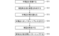
- FIG. 2 is a flowchart showing the flow of manufacturing the bonded substrate of the first embodiment.
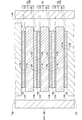
- FIG. 3 is a cross-sectional view schematically showing an object to be processed obtained during the manufacturing of the bonded substrate according to the first embodiment and a hot press machine used for manufacturing the bonded substrate according to the first embodiment.
- steps S11 to S16 shown in FIG. 2 are sequentially executed.
- step S11 a plurality of intermediate products 150 provided in the object to be processed 140 shown in FIG. 3 are prepared.
- Each of the intermediate products 150 included in the plurality of intermediate products 150 includes a silicon nitride ceramics substrate 110, a copper plate 111, a brazing material layer 162, a copper plate 113, and a brazing material layer 164.
- the copper plate 111 and the bonding layer 112 are omitted from the bonding substrate 100
- the copper plate 111 and the brazing material layer 162 are omitted from the intermediate product 150.
- the copper plate 113 and the bonding layer 114 are omitted from the bonding substrate 100
- the copper plate 113 and the brazing material layer 164 are omitted from the intermediate product 150.
- the brazing material layer 162 is between the one main surface 111A of the copper plate 111 and the first main surface 1101 of the silicon nitride ceramics substrate 110.
- the brazing material layer 164 is between the one main surface 113A of the copper plate 113 and the second main surface 1102 of the silicon nitride ceramics substrate 110.
- a paste containing an active metal brazing material and a solvent is prepared.
- the paste may further contain a binder, a dispersant, an antifoaming agent and the like.
- the prepared paste is screen-printed on the first main surface 1101 and the second main surface 1102 of the silicon nitride ceramic substrate 110, and on the first main surface 1101 and the second main surface 1102 of the silicon nitride ceramic substrate 110.
- the first and second screen-printed films are formed on the main surface 1102 of each.
- the solvent contained in the formed first and second screen printing films is volatilized.
- the braze layers 162 and 164 include an active metal braze.
- the brazing material layers 162 and 164 may be formed by a method different from this method.
- the active metal brazing material consists of powder.
- the active metal brazing material is, for example, at least one metal element selected from the group consisting of silver (Ag) and copper (Cu), and at least one selected from the group consisting of titanium (Ti) and zirconium (Zr). Includes some active metal elements.
- the active metal brazing material desirably comprises a metal powder containing silver and at least one selected from the group consisting of titanium hydride (TiH 2 ) powder and zirconium hydride (ZrH 2 ) powder.
- the active metal brazing material can be atomized at low cost, as in the case where the active metal brazing material is composed of a metal powder containing silver and at least one selected from the group consisting of titanium hydride powder and zirconium hydride powder. When the difficult alloy powder is not included, it becomes easy to atomize the active metal brazing material at low cost.
- the active metal brazing material is preferably a powder having an average particle size of 0.1 ⁇ m or more and 10 ⁇ m or less.
- the average particle size can be obtained by measuring the particle size distribution with a commercially available laser diffraction type particle size distribution measuring device and calculating D50 from the measured particle size distribution.
- the active metal brazing material having such a small average particle diameter allows the brazing material layers 162 and 164 to be thin.
- step S12 the coating 165 is formed so that the other main surface 111B of the copper plate 111 and the other main surface 113B of the copper plate 113 in the object 140 to be processed are covered with the coating 165.
- a coating liquid containing a release agent and a solvent is prepared.
- the coating liquid may further contain a binder, a dispersant, an antifoaming agent and the like.
- the solvent includes isopropyl alcohol and the like.
- the prepared coating liquid is sprayed toward the formation surface which is the other main surface 111B of the copper plate 111 or the other main surface 113B of the copper plate 113, and a spray film is formed on the formation surface.
- the coating liquid is preferably electrostatically applied to the formation surface. Thereby, it is possible to suppress the coating liquid from wrapping around other than the surface to be formed, and it is possible to reduce the loss of the coating liquid.
- the coating 165 includes a release agent.
- the coating 165 may be formed by a method different from this method. For example, instead of spraying the coating liquid containing the release agent onto the formation surface, screen printing of the paste containing the release agent may be performed.
- the thickness of the coating 165 is arbitrary, but is preferably 5 ⁇ m or more and 30 ⁇ m or less.
- the thickness of the coating 165 is smaller than this range, the other main surface 111B of the copper plate 111 and the other main surface 113B of the copper plate 113 tend to be exposed. Therefore, in step S14 described below, it is difficult to separate the copper plate 111 included in the uppermost intermediate product 150U and the copper plate 113 included in the lowermost intermediate product 150L from the upper punch 180 and the lower punch 181 respectively. Therefore, it tends to be difficult to separate the copper plate 111 included in the lower intermediate product 150 from the copper plate 113 included in the upper intermediate product 150.
- the thickness of the coating 165 is thicker than this range, it tends to take a long time to remove the coating 165 in step S15 described below.
- the release agent consists of powder.
- the release agent preferably includes crystals having a network layered structure, and more preferably a group consisting of boron nitride (BN) powder, graphite powder, molybdenum disulfide (MoS 2 ) powder and molybdenum dioxide (MoO 2 ) powder. It is particularly preferable that the boron nitride powder contains at least one selected from the group consisting of boron nitride powder having high heat resistance.
- the release agent desirably has an average particle size of 0.1 ⁇ m or more and 10 ⁇ m or less.
- the average particle size can be obtained by measuring the particle size distribution with a commercially available laser diffraction type particle size distribution measuring device and calculating D50 from the measured particle size distribution.
- the copper plate 111 and 113 are released from the mold on the other main surface 111B of the copper plate 111 and the other main surface 113B of the copper plate 113 when hot-bonded to the silicon nitride ceramic substrate 110.
- the shape of the powder of the agent is transferred, and the surface roughness of the other main surface 111B of the copper plate 111 and the other main surface 113B of the copper plate 113 tends to deteriorate.
- step S13 a plurality of intermediate products 150 are stacked in the thickness direction of the silicon nitride ceramic substrate 110. Thereby, the object 140 to be processed is obtained.
- step S14 the object 140 to be processed is heated by the heater 182 included in the hot pressing apparatus 170 while the object 140 to be processed is pressurized by the upper punch 180 and the lower punch 181 included in the hot pressing apparatus 170.
- hot pressing is performed on the plurality of intermediate products 150 included in the object 140 to be processed.
- the brazing material layer 162 changes to the bonding layer 112 that bonds the copper plate 111 to the silicon nitride ceramic substrate 110, and the copper plate 111 is hot-press bonded to the silicon nitride ceramic substrate 110.
- each intermediate product 150 includes a copper plate 111, a bonding layer 112, a copper plate 113, and a bonding layer 114, and the copper plates 111 and 113 are bonded to the silicon nitride ceramics substrate 110 via the bonding layers 112 and 114, respectively. Change to 100.
- step S14 desirably, the object 140 to be processed is pressed in the thickness direction of the silicon nitride ceramics substrate 110 according to a surface pressure profile in which the maximum surface pressure is 5 MPa or more and 25 MPa or less in a vacuum or an inert gas.
- the heating is performed according to a temperature profile in which the maximum temperature is 800 ° C. or more and 1000 ° C. or less, and desirably, the heating is performed according to a temperature profile in which the maximum temperature is 800 ° C. or more and 900 ° C. or less.
- the bonding layers 112 and 114 obtained in step S14 desirably have a thickness of 0.1 ⁇ m or more and 5 ⁇ m or less.
- the brazing material layers 162 and 164 are thinned, and the copper plates 111 and 113 are hot press bonded to the silicon nitride ceramic substrate 110, whereby the bonding layers 112 and 114 can be thinned.
- the stress caused by the presence of the bonding layers 112 and 114 can be reduced, and the deterioration of the durability of the bonding substrate 100 with respect to the thermal cycle due to the stress can be suppressed.
- the copper plates 111 and 113 can be plastically deformed by hot press bonding to the silicon nitride ceramics substrate 110 so as to cancel the warpage occurring in the bonded substrate 100. Thereby, the flatness of the bonded substrate 100 can be improved.
- step S12 By performing step S12 before performing step S14, the other main surface 111B of the copper plate 111 provided in the uppermost intermediate product 150U and the other major surface of the copper plate 113 provided in the lowermost intermediate product 150L are obtained.
- the copper plates 111 and 113 are hot-press bonded to the silicon nitride ceramics substrate 110 with the main surface 113B covered with the coating 165 containing a release agent. Therefore, when the copper plates 111 and 113 are hot-press bonded to the silicon nitride ceramics substrate 110, the other main surface 111B of the copper plate 111 provided in the uppermost intermediate product 150U and the lowermost intermediate product 150L are provided.
- the other main surface 113B of the copper plate 113 indirectly contacts the upper punch 181 and the upper punch 182 via the coating 165, and does not directly contact the upper punch 181 and the upper punch 182, respectively.
- the copper plate 111 and 113 are hot-press bonded to the silicon nitride ceramic substrate 110, the copper plate 111 provided in the intermediate product 150U in the uppermost stage and the copper plate 113 provided in the intermediate product 150L in the lowermost stage are respectively punched. It becomes easy to separate from the 180 and the lower punch 181. Thereby, the productivity of the bonded substrate stack 100 can be improved.
- step S12 is performed before step S14 is performed, the other main surface 111B of the copper plate 111 included in the lower intermediate product 150 of the two adjacent intermediate products 150 contains the release agent.
- the copper plates 111 and 113 are hot-press bonded to the silicon nitride ceramic substrate 110 while being covered with the coating 165. Therefore, when the copper plates 111 and 113 are hot-press bonded to the silicon nitride ceramics substrate 110, the other main surface 111B of the copper plate 111 provided in the intermediate product 150 in the lower stage is covered by the coating 165.
- the copper plate 113 provided in the intermediate product 150 in the upper stage in 150 is indirectly contacted, and the copper plate 113 provided in the intermediate product 150 in the upper stage is not directly contacted.
- the copper plate 111 included in the lower intermediate product 150 can be easily separated from the copper plate 113 included in the upper intermediate product 150. .. Thereby, the productivity of the bonded substrate stack 100 can be improved.
- step S13 By performing step S13 before performing step S14, it is possible to obtain a plurality of bonded substrates 100 at the same time. Thereby, the productivity of the bonded substrate stack 100 can be improved.
- the object to be processed 140 may include only one intermediate product 150. In that case, step S13 is not executed.
- step S15 the coating 165 is removed.
- the coating 165 is removed by sandblasting, scrubbing, rinsing, ultrasonic cleaning, polishing, or the like.
- step S16 the copper plate 111, the bonding layer 112, the copper plate 113, and the bonding layer 114 are patterned as needed. Patterning of the copper plate 111, the bonding layer 112, the copper plate 113, and the bonding layer 114 is performed, for example, by etching or the like.
Landscapes
- Engineering & Computer Science (AREA)
- Chemical & Material Sciences (AREA)
- Ceramic Engineering (AREA)
- Materials Engineering (AREA)
- Mechanical Engineering (AREA)
- Structural Engineering (AREA)
- Organic Chemistry (AREA)
- Ceramic Products (AREA)
- Powder Metallurgy (AREA)
Abstract
銅板が窒化ケイ素セラミックス基板にホットプレス接合された後に銅板を他の物体から分離することが容易になる接合基板の製造方法を提供する。少なくともひとつの中間品が準備される。各中間品は、窒化ケイ素セラミックス基板、銅板及びろう材層を備える。ろう材層は、銅板の一方の主面と窒化ケイ素セラミックス基板との間にある。続いて、離型剤を含む被覆が、当該被覆により銅板の他方の主面が覆われるように形成される。続いて、少なくともひとつの中間品に対してホットプレスが行われる。これにより、ろう材層が、銅板を窒化ケイ素セラミックス基板に接合する接合層に変化する。また、各中間品が、窒化ケイ素セラミックス基板、銅板及び接合層を備え銅板が接合層を介して窒化ケイ素セラミックス基板に接合されている接合基板に変化する。続いて、被覆が除去される。
Description
本発明は、接合基板の製造方法に関する。
窒化ケイ素セラミックスは、高い熱伝導性及び高い絶縁性を有する。このため、銅板が窒化ケイ素セラミックス基板に接合された接合基板は、パワー半導体素子が実装される絶縁放熱基板として好適に用いられる。
当該接合基板は、多くの場合は、ろう材層が銅板と窒化ケイ素セラミックス基板との間にある中間品を作製し、作製した中間品を熱処理することにより製造される。中間品が熱処理される際には、ろう材層が、銅板を窒化ケイ素セラミックス基板に接合する接合層に変化する。また、中間品が、銅板が接合層を介して窒化ケイ素セラミックス基板に接合された接合基板に変化する。
中間品を熱処理する際に中間品に対してホットプレスを行うことも提案されている。例えば、特許文献1に記載された技術においては、接合基板が、窒化珪素基板の一方主面に接合層を介して銅板が接合された構成を有する(段落0024-0025)。接合基板は、窒化珪素基板の一方主面上にろう材を塗布した後にろう材の塗布面に銅板を重ね合わせ、加熱および加圧することによって得られる(段落0024-0025)。
接合基板が製造される際に中間品に対してホットプレスが行われた場合は、銅板が窒化ケイ素セラミックス基板にホットプレス接合された後に銅板を他の物体から分離することが困難になる場合がある。例えば、銅板が中間品を加圧するパンチに固着し銅板をパンチから分離することが困難になる場合がある。また、複数の中間品が窒化ケイ素セラミックス基板の厚さ方向に積み重ねられた状態で複数の中間品に対してホットプレスが行われた場合は、隣接するふたつの中間品にそれぞれ備えられるふたつの銅板を互いに分離することが困難になる場合がある。
本発明は、この問題を考慮してなされた。本発明が解決しようとする課題は、銅板が窒化ケイ素セラミックス基板にホットプレス接合された後に銅板を他の物体から分離することが容易になる接合基板の製造方法を提供することである。
本発明は、接合基板の製造方法に向けられる。
少なくともひとつの中間品が準備される。各中間品は、窒化ケイ素セラミックス基板、銅板及びろう材層を備える。ろう材層は、銅板の一方の主面と窒化ケイ素セラミックス基板との間にある。
続いて、離型剤を含む被覆が、当該被覆により銅板の他方の主面が覆われるように形成される。
続いて、少なくともひとつの中間品に対してホットプレスが行われる。これにより、ろう材層が、銅板を窒化ケイ素セラミックス基板に接合する接合層に変化する。また、各中間品が、窒化ケイ素セラミックス基板、銅板及び接合層を備え銅板が接合層を介して窒化ケイ素セラミックス基板に接合されている接合基板に変化する。
続いて、被覆が除去される。
本発明によれば、銅板の他方の主面が離型剤を含む被覆に覆われた状態で、銅板が窒化ケイ素セラミックス基板にホットプレス接合される。このため、銅板が窒化ケイ素セラミックス基板にホットプレス接合された後に銅板を他の物体から分離することが容易になる。これにより、接合基板の生産性を向上することができる。
この発明の目的、特徴、局面及び利点は、以下の詳細な説明と添付図面とによって、より明白となる。
1 接合基板
図1は、第1実施形態の接合基板を模式的に図示する断面図である。
図1は、第1実施形態の接合基板を模式的に図示する断面図である。
図1に図示される第1実施形態の接合基板100は、窒化ケイ素セラミックス基板110、銅板111、接合層112、銅板113及び接合層114を備える。接合基板100がこれらの要素以外の要素を備えてもよい。銅板111及び接合層112の組、並びに銅板113及び接合層114の組の片方の組が省略されてもよい。
銅板111及び113は、それぞれ接合層112及び114を介して窒化ケイ素セラミックス基板110に接合されている。銅板111及び113は、それぞれ接合層112及び114により窒化ケイ素セラミックス基板110の互いに反対の方向を向く第1の主面1101及び第2の主面1102にろう付けされている。
接合基板100は、どのように用いられてもよいが、例えばパワー半導体素子が実装される絶縁放熱基板として用いられる。
2 接合基板の製造方法
図2は、第1実施形態の接合基板の製造の流れを示すフローチャートである。図3は、第1実施形態の接合基板の製造中に得られる被処理物、及び第1実施形態の接合基板の製造に使用されるホットプレス装置を模式的に図示する断面図である。
図2は、第1実施形態の接合基板の製造の流れを示すフローチャートである。図3は、第1実施形態の接合基板の製造中に得られる被処理物、及び第1実施形態の接合基板の製造に使用されるホットプレス装置を模式的に図示する断面図である。
第1実施形態の接合基板100の製造においては、図2に図示される工程S11からS16までが順次に実行される。
工程S11においては、図3に図示される被処理物140に備えられる複数の中間品150が準備される。
複数の中間品150に含まれる各中間品150は、窒化ケイ素セラミックス基板110、銅板111、ろう材層162、銅板113及びろう材層164を備える。接合基板100から銅板111及び接合層112が省略される場合は、中間品150から銅板111及びろう材層162が省略される。接合基板100から銅板113及び接合層114が省略される場合は、中間品150から銅板113及びろう材層164が省略される。
ろう材層162は、銅板111の一方の主面111Aと窒化ケイ素セラミックス基板110の第1の主面1101との間にある。ろう材層164は、銅板113の一方の主面113Aと窒化ケイ素セラミックス基板110の第2の主面1102との間にある。
ろう材層162及び164が形成される際には、活性金属ろう材及び溶剤を含むペーストが調製される。ペーストがバインダ、分散剤、消泡剤等をさらに含んでもよい。続いて、調製されたペーストが窒化ケイ素セラミックス基板110の第1の主面1101上及び第2の主面1102上にスクリーン印刷され、窒化ケイ素セラミックス基板110の第1の主面1101上及び第2の主面1102上にそれぞれ第1及び第2のスクリーン印刷膜が形成される。続いて、形成された第1及び第2のスクリーン印刷膜に含まれる溶剤が揮発させられる。これにより、第1及び第2のスクリーン印刷膜が、それぞれろう材層162及び164に変化する。ろう材層162及び164は、活性金属ろう材を含む。ろう材層162及び164がこの方法とは異なる方法により形成されてもよい。
活性金属ろう材は、粉末からなる。活性金属ろう材は、例えば、銀(Ag)及び銅(Cu)からなる群より選択される少なくとも1種の金属元素、並びにチタン(Ti)及びジルコニウム(Zr)からなる群より選択される少なくとも1種の活性金属元素を含む。活性金属ろう材は、望ましくは、銀を含む金属粉末、並びに水素化チタン(TiH2)粉末及び水素化ジルコニウム(ZrH2)粉末からなる群より選択される少なくとも1種からなる。活性金属ろう材が銀を含む金属粉末、並びに水素化チタン粉末及び水素化ジルコニウム粉末からなる群より選択される少なくとも1種からなる場合のように活性金属ろう材が低コストで微粒化することが困難な合金粉末を含まない場合は、活性金属ろう材を低コストで微粒化することが容易になる。
活性金属ろう材は、望ましくは、0.1μm以上10μm以下の平均粒子径を有する粉末からなる。平均粒子径は、市販のレーザー回折式の粒度分布測定装置により粒度分布を測定し、測定した粒度分布からD50を算出することにより得ることができる。活性金属ろう材がこのように小さい平均粒子径を有することにより、ろう材層162及び164を薄くすることができる。
工程S12においては、被処理物140において銅板111の他方の主面111B及び銅板113の他方の主面113Bが被覆165により覆われるように被覆165が形成される。
被覆165が形成される際には、離型剤及び溶剤を含む被覆液が調製される。被覆液が、バインダ、分散剤、消泡剤等をさらに含んでもよい。溶剤は、イソプロピルアルコール等を含む。続いて、調製された被覆液が銅板111の他方の主面111B又は銅板113の他方の主面113Bである被形成面に向かってスプレーされ、当該被形成面にスプレー膜が形成される。スプレー膜が被形成面に形成される際には、望ましくは被覆液が被形成面に静電塗布される。これにより、被覆液が被形成面以外に回り込むことを抑制することができ、被覆液のロスを少なくすることができる。続いて、形成されたスプレー膜に含まれる溶剤が揮発させられる。これにより、スプレー膜が被覆165に変化する。被覆165は、離型剤を含む。被覆165がこの方法とは異なる方法により形成されてもよい。例えば、離型剤を含む被覆液を被形成面に向かってスプレーすることに代えて、離型剤を含むペーストを被形成面にスクリーン印刷することが行われてもよい。
被覆165の厚さは、任意であるが、望ましくは5μm以上30μm以下である。被覆165の厚さがこの範囲より薄い場合は、銅板111の他方の主面111B及び銅板113の他方の主面113Bが露出しやすくなる傾向が現れる。このため、下述する工程S14において、最上段の中間品150Uに備えられる銅板111、及び最下段の中間品150Lに備えられる銅板113を、それぞれ上パンチ180及び下パンチ181から分離することが困難になり、下段の中間品150に備えられる銅板111を上段の中間品150に備えられる銅板113から分離することが困難になる傾向が現れる。一方、被覆165の厚さがこの範囲より厚い場合は、下述する工程S15において、被覆165を除去するのに長時間を要する傾向が現れる。
離型剤は、粉末からなる。離型剤は、望ましくは、網目層状構造を有する結晶を含み、さらに望ましくは、窒化ホウ素(BN)粉末、黒鉛粉末、二硫化モリブデン(MoS2)粉末及び二酸化モリブデン(MoO2)粉末からなる群より選択される少なくとも1種を含み、特に望ましくは高い耐熱性を有する窒化ホウ素粉末からなる。
離型剤は、望ましくは0.1μm以上10μm以下の平均粒子径を有する。平均粒子径は、市販のレーザー回折式の粒度分布測定装置により粒度分布を測定し、測定した粒度分布からD50を算出することにより得ることができる。平均粒子径がこの範囲より大きい場合は、銅板111及び113が窒化ケイ素セラミックス基板110にホットプレス接合される際に、銅板111の他方の主面111B及び銅板113の他方の主面113Bに離型剤の粉末の形状が転写され、銅板111の他方の主面111B及び銅板113の他方の主面113Bの表面粗さが悪化する傾向が現れる。
工程S13においては、複数の中間品150が窒化ケイ素セラミックス基板110の厚さ方向に積み重ねられる。これにより、被処理物140が得られる。
工程S14においては、被処理物140がホットプレス装置170に備えられる上パンチ180及び下パンチ181により加圧された状態で被処理物140がホットプレス装置170に備えられるヒーター182により加熱される。これにより、被処理物140に備えられる複数の中間品150に対してホットプレスが行われる。その結果として、ろう材層162が銅板111を窒化ケイ素セラミックス基板110に接合する接合層112に変化し、銅板111が窒化ケイ素セラミックス基板110にホットプレス接合される。また、ろう材層164が銅板113を窒化ケイ素セラミックス基板110に接合する接合層114に変化し、銅板113が窒化ケイ素セラミックス基板110にホットプレス接合される。そして、各中間品150が、銅板111、接合層112、銅板113及び接合層114を備え、銅板111及び113がそれぞれ接合層112及び114を介して窒化ケイ素セラミックス基板110に接合されている接合基板100に変化する。
工程S14においては、望ましくは、被処理物140が、真空中又は不活性ガス中で、最高面圧が5MPa以上25MPa以下となる面圧プロファイルにしたがって窒化ケイ素セラミックス基板110の厚さ方向に加圧され、最高温度が800℃以上1000℃以下となる温度プロファイルにしたがって加熱され、望ましくは最高温度が800℃以上900℃以下となる温度プロファイルにしたがって加熱される。
工程S14において得られる接合層112及び114は、望ましくは、0.1μm以上5μm以下の厚さを有する。
銅板111及び113が窒化ケイ素セラミックス基板110にホットプレス接合されることにより、接合層112中、接合層114中及び窒化ケイ素セラミックス基板110中の欠陥を減らすことができる。これにより、欠陥に起因する、接合基板100の絶縁不良を抑制することができる。
また、ろう材層162及び164が薄くなり、銅板111及び113が窒化ケイ素セラミックス基板110にホットプレス接合されることにより、接合層112及び114を薄くすることができる。これにより、接合層112及び114の存在により生じる応力を小さくすることができ、応力に起因する、冷熱サイクルに対する接合基板100の耐久性の低下を抑制することができる。
また、銅板111及び113が窒化ケイ素セラミックス基板110にホットプレス接合されることにより、接合基板100に生じるそりを打ち消すように銅板111及び113を塑性変形させることができる。これにより、接合基板100の平坦性を向上することができる。
工程S14が実行される前に工程S12が実行されることにより、最上段の中間品150Uに備えられる銅板111の他方の主面111B、及び最下段の中間品150Lに備えられる銅板113の他方の主面113Bが離型剤を含む被覆165に覆われた状態で、銅板111及び113が窒化ケイ素セラミックス基板110にホットプレス接合される。このため、銅板111及び113が窒化ケイ素セラミックス基板110にホットプレス接合される際に、最上段の中間品150Uに備えられる銅板111の他方の主面111B、及び最下段の中間品150Lに備えられる銅板113の他方の主面113Bは、それぞれ、被覆165を介して上パンチ181及び上パンチ182に間接的に接触し、上パンチ181及び上パンチ182に直接的に接触しない。これにより、銅板111及び113が窒化ケイ素セラミックス基板110にホットプレス接合された後に、最上段の中間品150Uに備えられる銅板111、及び最下段の中間品150Lに備えられる銅板113を、それぞれ上パンチ180及び下パンチ181から分離することが容易になる。これにより、接合基板100の生産性を向上することができる。
また、工程S14が実行される前に工程S12が実行されることにより、隣接するふたつの中間品150中の下段の中間品150に備えられる銅板111の他方の主面111Bが離型剤を含む被覆165に覆われた状態で、銅板111及び113が窒化ケイ素セラミックス基板110にホットプレス接合される。このため、銅板111及び113が窒化ケイ素セラミックス基板110にホットプレス接合される際に、下段の中間品150に備えられる銅板111の他方の主面111Bは、被覆165を介して当該ふたつの中間品150中の上段の中間品150に備えられる銅板113に間接的に接触し、上段の中間品150に備えられる銅板113に直接的に接触しない。これにより、銅板111及び113が窒化ケイ素セラミックス基板110にホットプレス接合された後に、下段の中間品150に備えられる銅板111を上段の中間品150に備えられる銅板113から分離することが容易になる。これにより、接合基板100の生産性を向上することができる。
工程S14が実行される前に工程S13が実行されることにより、複数の接合基板100を同時に得ることができる。これにより、接合基板100の生産性を向上することができる。ただし、被処理物140がただひとつの中間品150を備えてもよい。その場合は、工程S13が実行されない。
工程S15においては、被覆165が除去される。被覆165の除去は、サンドブラスト、こすり洗い、すすぎ、超音波洗浄、研磨等により行われる。
工程S16においては、銅板111、接合層112、銅板113及び接合層114が必要に応じてパターニングされる。銅板111、接合層112、銅板113及び接合層114のパターニングは、例えばエッチング等により行われる。
この発明は詳細に説明されたが、上記した説明は、すべての局面において、例示であって、この発明がそれに限定されるものではない。例示されていない無数の変形例が、この発明の範囲から外れることなく想定され得るものと解される。
100 接合基板
110 窒化ケイ素セラミックス基板
111 銅板
112 接合層
113 銅板
114 接合層
150 中間品
162 ろう材層
164 ろう材層
165 被覆
110 窒化ケイ素セラミックス基板
111 銅板
112 接合層
113 銅板
114 接合層
150 中間品
162 ろう材層
164 ろう材層
165 被覆
Claims (10)
- a) 各中間品が、窒化ケイ素セラミックス基板と、一方の主面及び他方の主面を有する銅板と、前記一方の主面と前記窒化ケイ素セラミックス基板との間にあるろう材層と、を備える少なくともひとつの中間品を準備する工程と、
b) 離型剤を含む被覆を、前記被覆により前記他方の主面が覆われるように形成する工程と、
c) 前記少なくともひとつの中間品に対してホットプレスを行い、前記ろう材層を、前記銅板を前記窒化ケイ素セラミックス基板に接合する接合層に変化させ、前記各中間品を、前記窒化ケイ素セラミックス基板、前記銅板及び前記接合層を備え前記銅板が前記接合層を介して前記窒化ケイ素セラミックス基板に接合されている接合基板に変化させる工程と、
d) 前記被覆を除去する工程と、
を備える接合基板の製造方法。 - 前記少なくともひとつの中間品は、複数の中間品であり、
e) 工程b)の後であって工程c)の前に前記窒化ケイ素セラミックス基板の厚さ方向に前記複数の中間品を積み重ねる工程
をさらに備える請求項1の接合基板の製造方法。 - 前記窒化ケイ素セラミックス基板は、第1の主面及び第2の主面を有し、
前記銅板は、第1の銅板であり、
前記ろう材層は、第1のろう材層であり、前記第1の銅板の一方の主面と前記第1の主面との間にあり、
前記各中間品は、一方の主面及び他方の主面を有する第2の銅板と、前記第2の銅板の一方の主面と前記第2の主面との間にある第2のろう材層と、をさらに備え、
工程b)は、前記被覆により前記第2の銅板の他方の主面がさらに覆われるように前記被覆を形成する
請求項1又は2の接合基板の製造方法。 - 前記離型剤は、網目層状構造を有する結晶を含む
請求項1から3までのいずれかの接合基板の製造方法。 - 前記離型剤は、窒化ホウ素粉末、黒鉛粉末、二硫化モリブデン粉末及び二酸化モリブデン粉末からなる群より選択される少なくとも1種を含む
請求項1から4までのいずれかの接合基板の製造方法。 - 工程c)は、 前記少なくともひとつの中間品を、最高面圧が5MPa以上25MPa以下となる面圧プロファイルにしたがって前記窒化ケイ素セラミックス基板の厚さ方向に加圧し、最高温度が800℃以上1000℃以下となる温度プロファイルにしたがって加熱する
請求項1から5までのいずれかの接合基板の製造方法。 - 前記ろう材層は、銀を含む金属粉末、並びに水素化チタン粉末及び水素化ジルコニウム粉末からなる群より選ばれる少なくとも1種を含む
請求項1から6までのいずれかの接合基板の製造方法。 - 前記ろう材層は、0.1μm以上10μm以下の平均粒子径を有する粉末からなる活性金属ろう材を含む
請求項1から7までのいずれかの接合基板の製造方法。 - 前記接合層は、0.1μm以上5μm以下の厚さを有する
請求項1から8までのいずれかの接合基板の製造方法。 - e) 工程d)の後に前記銅板をパターニングする工程
をさらに備える請求項1から9までのいずれかの接合基板の製造方法。
Priority Applications (3)
| Application Number | Priority Date | Filing Date | Title |
|---|---|---|---|
| JP2020557095A JPWO2020105160A1 (ja) | 2018-11-22 | 2018-11-22 | 接合基板の製造方法 |
| PCT/JP2018/043124 WO2020105160A1 (ja) | 2018-11-22 | 2018-11-22 | 接合基板の製造方法 |
| JP2022117775A JP7453288B2 (ja) | 2018-11-22 | 2022-07-25 | 接合基板の製造方法 |
Applications Claiming Priority (1)
| Application Number | Priority Date | Filing Date | Title |
|---|---|---|---|
| PCT/JP2018/043124 WO2020105160A1 (ja) | 2018-11-22 | 2018-11-22 | 接合基板の製造方法 |
Publications (1)
| Publication Number | Publication Date |
|---|---|
| WO2020105160A1 true WO2020105160A1 (ja) | 2020-05-28 |
Family
ID=70774464
Family Applications (1)
| Application Number | Title | Priority Date | Filing Date |
|---|---|---|---|
| PCT/JP2018/043124 Ceased WO2020105160A1 (ja) | 2018-11-22 | 2018-11-22 | 接合基板の製造方法 |
Country Status (2)
| Country | Link |
|---|---|
| JP (2) | JPWO2020105160A1 (ja) |
| WO (1) | WO2020105160A1 (ja) |
Cited By (3)
| Publication number | Priority date | Publication date | Assignee | Title |
|---|---|---|---|---|
| CN112679220A (zh) * | 2020-12-30 | 2021-04-20 | 中国电子科技集团公司第十三研究所 | 氮化硅陶瓷覆铜基板及其制备方法 |
| CN113385592A (zh) * | 2021-06-11 | 2021-09-14 | 嘉兴博朗金属科技有限公司 | 一种彩色铜及其制造方法 |
| DE112022002201T5 (de) | 2021-06-11 | 2024-03-14 | NGK Electronics Devices, Inc. | Verfahren zur Herstellung eines gebondeten Substrats, Verfahren zur Herstellung eines Schaltungssubstrats und Schaltungssubstrat |
Families Citing this family (1)
| Publication number | Priority date | Publication date | Assignee | Title |
|---|---|---|---|---|
| JP7658020B1 (ja) | 2023-11-02 | 2025-04-07 | トーホーテック株式会社 | 水素化チタン粉末及び、活性金属ろう材 |
Citations (6)
| Publication number | Priority date | Publication date | Assignee | Title |
|---|---|---|---|---|
| JP2002314220A (ja) * | 2001-04-11 | 2002-10-25 | Denki Kagaku Kogyo Kk | 回路基板の製造方法 |
| JP2002356376A (ja) * | 2001-05-31 | 2002-12-13 | Kyocera Corp | 配線基板及びその製造方法 |
| JP2007197229A (ja) * | 2006-01-24 | 2007-08-09 | National Institute Of Advanced Industrial & Technology | 高熱伝導窒化ケイ素基板とその製造方法 |
| JP2013247158A (ja) * | 2012-05-23 | 2013-12-09 | Denki Kagaku Kogyo Kk | セラミックス回路基板 |
| JP2017035805A (ja) * | 2015-08-07 | 2017-02-16 | Jx金属株式会社 | 金属セラミック接合基板及び、その製造方法 |
| JP2018008869A (ja) * | 2016-06-30 | 2018-01-18 | 三菱マテリアル株式会社 | 銅/セラミックス接合体、及び、絶縁回路基板 |
-
2018
- 2018-11-22 JP JP2020557095A patent/JPWO2020105160A1/ja active Pending
- 2018-11-22 WO PCT/JP2018/043124 patent/WO2020105160A1/ja not_active Ceased
-
2022
- 2022-07-25 JP JP2022117775A patent/JP7453288B2/ja active Active
Patent Citations (6)
| Publication number | Priority date | Publication date | Assignee | Title |
|---|---|---|---|---|
| JP2002314220A (ja) * | 2001-04-11 | 2002-10-25 | Denki Kagaku Kogyo Kk | 回路基板の製造方法 |
| JP2002356376A (ja) * | 2001-05-31 | 2002-12-13 | Kyocera Corp | 配線基板及びその製造方法 |
| JP2007197229A (ja) * | 2006-01-24 | 2007-08-09 | National Institute Of Advanced Industrial & Technology | 高熱伝導窒化ケイ素基板とその製造方法 |
| JP2013247158A (ja) * | 2012-05-23 | 2013-12-09 | Denki Kagaku Kogyo Kk | セラミックス回路基板 |
| JP2017035805A (ja) * | 2015-08-07 | 2017-02-16 | Jx金属株式会社 | 金属セラミック接合基板及び、その製造方法 |
| JP2018008869A (ja) * | 2016-06-30 | 2018-01-18 | 三菱マテリアル株式会社 | 銅/セラミックス接合体、及び、絶縁回路基板 |
Cited By (4)
| Publication number | Priority date | Publication date | Assignee | Title |
|---|---|---|---|---|
| CN112679220A (zh) * | 2020-12-30 | 2021-04-20 | 中国电子科技集团公司第十三研究所 | 氮化硅陶瓷覆铜基板及其制备方法 |
| CN113385592A (zh) * | 2021-06-11 | 2021-09-14 | 嘉兴博朗金属科技有限公司 | 一种彩色铜及其制造方法 |
| CN113385592B (zh) * | 2021-06-11 | 2022-07-01 | 嘉兴博朗金属科技有限公司 | 一种彩色铜及其制造方法 |
| DE112022002201T5 (de) | 2021-06-11 | 2024-03-14 | NGK Electronics Devices, Inc. | Verfahren zur Herstellung eines gebondeten Substrats, Verfahren zur Herstellung eines Schaltungssubstrats und Schaltungssubstrat |
Also Published As
| Publication number | Publication date |
|---|---|
| JP2022166010A (ja) | 2022-11-01 |
| JP7453288B2 (ja) | 2024-03-19 |
| JPWO2020105160A1 (ja) | 2021-10-14 |
Similar Documents
| Publication | Publication Date | Title |
|---|---|---|
| JP7453288B2 (ja) | 接合基板の製造方法 | |
| CN103648766B (zh) | 层叠体和层叠体的制造方法 | |
| JP6100605B2 (ja) | 多層クラッド材の製造方法 | |
| JP2019104680A5 (ja) | ||
| JP5183294B2 (ja) | 焼結されたパワー半導体基板並びにそのための製造方法 | |
| US20180090414A1 (en) | Ceramic substrate manufacturing method and ceramic substrate manufactured thereby | |
| WO2010082540A1 (ja) | 熱電変換モジュールの製造方法及び熱電変換モジュール | |
| US12249547B2 (en) | Bonded substrate and bonded substrate manufacturing method | |
| JP2018135251A (ja) | パワーモジュール用基板の製造方法 | |
| JP2008192823A (ja) | 回路基板の製造装置及び製造方法、その製造方法に用いられるクッションシート | |
| KR20170048999A (ko) | 세라믹 기판 제조 방법 및 이 제조방법으로 제조된 세라믹 기판 | |
| JP7197677B2 (ja) | 接合基板 | |
| KR20170049000A (ko) | 세라믹 기판 제조 방법 및 이 제조방법으로 제조된 세라믹 기판 | |
| US7182899B2 (en) | Manufacturing method of ceramic electronic components and its manufacturing equipment | |
| JP7289910B2 (ja) | 接合基板及び接合基板の製造方法 | |
| JP7431857B2 (ja) | 接合基板の製造方法 | |
| JP6969471B2 (ja) | 絶縁回路基板 | |
| JP2010277809A (ja) | 加熱ヒータおよびそれを備えた装置 | |
| JP7460656B2 (ja) | 接合基板の製造方法 | |
| JP6853443B2 (ja) | パワーモジュール用基板の製造方法 | |
| KR20160126926A (ko) | 세라믹 기판 제조 방법 및 이 제조방법으로 제조된 세라믹 기판 | |
| JP3712378B2 (ja) | 端子付き回路基板及びその製造方法 | |
| JP7363583B2 (ja) | 絶縁回路基板の製造方法 | |
| JP6396703B2 (ja) | 半導体素子用放熱部品の製造方法 | |
| JP2013041895A (ja) | 接続シート |
Legal Events
| Date | Code | Title | Description |
|---|---|---|---|
| 121 | Ep: the epo has been informed by wipo that ep was designated in this application |
Ref document number: 18940741 Country of ref document: EP Kind code of ref document: A1 |
|
| ENP | Entry into the national phase |
Ref document number: 2020557095 Country of ref document: JP Kind code of ref document: A |
|
| NENP | Non-entry into the national phase |
Ref country code: DE |
|
| 122 | Ep: pct application non-entry in european phase |
Ref document number: 18940741 Country of ref document: EP Kind code of ref document: A1 |