WO2020104892A1 - 半導体装置及び充電制御システム - Google Patents
半導体装置及び充電制御システムInfo
- Publication number
- WO2020104892A1 WO2020104892A1 PCT/IB2019/059682 IB2019059682W WO2020104892A1 WO 2020104892 A1 WO2020104892 A1 WO 2020104892A1 IB 2019059682 W IB2019059682 W IB 2019059682W WO 2020104892 A1 WO2020104892 A1 WO 2020104892A1
- Authority
- WO
- WIPO (PCT)
- Prior art keywords
- oxide
- insulator
- conductor
- transistor
- secondary battery
- Prior art date
- Legal status (The legal status is an assumption and is not a legal conclusion. Google has not performed a legal analysis and makes no representation as to the accuracy of the status listed.)
- Ceased
Links
Images















Classifications
-
- H—ELECTRICITY
- H01—ELECTRIC ELEMENTS
- H01M—PROCESSES OR MEANS, e.g. BATTERIES, FOR THE DIRECT CONVERSION OF CHEMICAL ENERGY INTO ELECTRICAL ENERGY
- H01M10/00—Secondary cells; Manufacture thereof
- H01M10/42—Methods or arrangements for servicing or maintenance of secondary cells or secondary half-cells
- H01M10/44—Methods for charging or discharging
-
- H—ELECTRICITY
- H02—GENERATION; CONVERSION OR DISTRIBUTION OF ELECTRIC POWER
- H02J—ELECTRIC POWER NETWORKS; CIRCUIT ARRANGEMENTS OR SYSTEMS FOR SUPPLYING OR DISTRIBUTING ELECTRIC POWER; SYSTEMS FOR STORING ELECTRIC ENERGY
- H02J7/00—Circuit arrangements for charging or discharging batteries or for supplying loads from batteries
- H02J7/60—Circuit arrangements for charging or discharging batteries or for supplying loads from batteries including safety or protection arrangements
- H02J7/61—Circuit arrangements for charging or discharging batteries or for supplying loads from batteries including safety or protection arrangements against overcharge
-
- H—ELECTRICITY
- H01—ELECTRIC ELEMENTS
- H01M—PROCESSES OR MEANS, e.g. BATTERIES, FOR THE DIRECT CONVERSION OF CHEMICAL ENERGY INTO ELECTRICAL ENERGY
- H01M10/00—Secondary cells; Manufacture thereof
- H01M10/42—Methods or arrangements for servicing or maintenance of secondary cells or secondary half-cells
- H01M10/48—Accumulators combined with arrangements for measuring, testing or indicating the condition of cells, e.g. the level or density of the electrolyte
-
- H—ELECTRICITY
- H02—GENERATION; CONVERSION OR DISTRIBUTION OF ELECTRIC POWER
- H02H—EMERGENCY PROTECTIVE CIRCUIT ARRANGEMENTS
- H02H7/00—Emergency protective circuit arrangements specially adapted for specific types of electric machines or apparatus or for sectionalised protection of cable or line systems, and effecting automatic switching in the event of an undesired change from normal working conditions
- H02H7/18—Emergency protective circuit arrangements specially adapted for specific types of electric machines or apparatus or for sectionalised protection of cable or line systems, and effecting automatic switching in the event of an undesired change from normal working conditions for batteries; for accumulators
-
- H—ELECTRICITY
- H02—GENERATION; CONVERSION OR DISTRIBUTION OF ELECTRIC POWER
- H02J—ELECTRIC POWER NETWORKS; CIRCUIT ARRANGEMENTS OR SYSTEMS FOR SUPPLYING OR DISTRIBUTING ELECTRIC POWER; SYSTEMS FOR STORING ELECTRIC ENERGY
- H02J50/00—Circuit arrangements or systems for wireless supply or distribution of electric power
- H02J50/10—Circuit arrangements or systems for wireless supply or distribution of electric power using inductive coupling
-
- H—ELECTRICITY
- H02—GENERATION; CONVERSION OR DISTRIBUTION OF ELECTRIC POWER
- H02J—ELECTRIC POWER NETWORKS; CIRCUIT ARRANGEMENTS OR SYSTEMS FOR SUPPLYING OR DISTRIBUTING ELECTRIC POWER; SYSTEMS FOR STORING ELECTRIC ENERGY
- H02J7/00—Circuit arrangements for charging or discharging batteries or for supplying loads from batteries
- H02J7/02—Circuit arrangements for charging or discharging batteries or for supplying loads from batteries for charging batteries from AC mains by converters
- H02J7/04—Regulation of charging current or voltage
- H02J7/06—Regulation of charging current or voltage using discharge tubes or semiconductor devices
-
- H—ELECTRICITY
- H02—GENERATION; CONVERSION OR DISTRIBUTION OF ELECTRIC POWER
- H02J—ELECTRIC POWER NETWORKS; CIRCUIT ARRANGEMENTS OR SYSTEMS FOR SUPPLYING OR DISTRIBUTING ELECTRIC POWER; SYSTEMS FOR STORING ELECTRIC ENERGY
- H02J7/00—Circuit arrangements for charging or discharging batteries or for supplying loads from batteries
- H02J7/60—Circuit arrangements for charging or discharging batteries or for supplying loads from batteries including safety or protection arrangements
- H02J7/663—Circuit arrangements for charging or discharging batteries or for supplying loads from batteries including safety or protection arrangements using battery or load disconnect circuits
-
- H—ELECTRICITY
- H02—GENERATION; CONVERSION OR DISTRIBUTION OF ELECTRIC POWER
- H02J—ELECTRIC POWER NETWORKS; CIRCUIT ARRANGEMENTS OR SYSTEMS FOR SUPPLYING OR DISTRIBUTING ELECTRIC POWER; SYSTEMS FOR STORING ELECTRIC ENERGY
- H02J7/00—Circuit arrangements for charging or discharging batteries or for supplying loads from batteries
- H02J7/70—Circuit arrangements for charging or discharging batteries or for supplying loads from batteries characterised by the mechanical construction
-
- H—ELECTRICITY
- H10—SEMICONDUCTOR DEVICES; ELECTRIC SOLID-STATE DEVICES NOT OTHERWISE PROVIDED FOR
- H10D—INORGANIC ELECTRIC SEMICONDUCTOR DEVICES
- H10D30/00—Field-effect transistors [FET]
- H10D30/60—Insulated-gate field-effect transistors [IGFET]
- H10D30/62—Fin field-effect transistors [FinFET]
- H10D30/6211—Fin field-effect transistors [FinFET] having fin-shaped semiconductor bodies integral with the bulk semiconductor substrates
-
- H—ELECTRICITY
- H10—SEMICONDUCTOR DEVICES; ELECTRIC SOLID-STATE DEVICES NOT OTHERWISE PROVIDED FOR
- H10D—INORGANIC ELECTRIC SEMICONDUCTOR DEVICES
- H10D30/00—Field-effect transistors [FET]
- H10D30/60—Insulated-gate field-effect transistors [IGFET]
- H10D30/67—Thin-film transistors [TFT]
- H10D30/6729—Thin-film transistors [TFT] characterised by the electrodes
- H10D30/673—Thin-film transistors [TFT] characterised by the electrodes characterised by the shapes, relative sizes or dispositions of the gate electrodes
- H10D30/6733—Multi-gate TFTs
- H10D30/6734—Multi-gate TFTs having gate electrodes arranged on both top and bottom sides of the channel, e.g. dual-gate TFTs
-
- H—ELECTRICITY
- H10—SEMICONDUCTOR DEVICES; ELECTRIC SOLID-STATE DEVICES NOT OTHERWISE PROVIDED FOR
- H10D—INORGANIC ELECTRIC SEMICONDUCTOR DEVICES
- H10D30/00—Field-effect transistors [FET]
- H10D30/60—Insulated-gate field-effect transistors [IGFET]
- H10D30/67—Thin-film transistors [TFT]
- H10D30/674—Thin-film transistors [TFT] characterised by the active materials
- H10D30/6755—Oxide semiconductors, e.g. zinc oxide, copper aluminium oxide or cadmium stannate
-
- H—ELECTRICITY
- H10—SEMICONDUCTOR DEVICES; ELECTRIC SOLID-STATE DEVICES NOT OTHERWISE PROVIDED FOR
- H10D—INORGANIC ELECTRIC SEMICONDUCTOR DEVICES
- H10D30/00—Field-effect transistors [FET]
- H10D30/60—Insulated-gate field-effect transistors [IGFET]
- H10D30/67—Thin-film transistors [TFT]
- H10D30/6757—Thin-film transistors [TFT] characterised by the structure of the channel, e.g. transverse or longitudinal shape or doping profile
-
- H—ELECTRICITY
- H10—SEMICONDUCTOR DEVICES; ELECTRIC SOLID-STATE DEVICES NOT OTHERWISE PROVIDED FOR
- H10W—GENERIC PACKAGES, INTERCONNECTIONS, CONNECTORS OR OTHER CONSTRUCTIONAL DETAILS OF DEVICES COVERED BY CLASS H10
- H10W20/00—Interconnections in chips, wafers or substrates
- H10W20/40—Interconnections external to wafers or substrates, e.g. back-end-of-line [BEOL] metallisations or vias connecting to gate electrodes
- H10W20/495—Capacitive arrangements or effects of, or between wiring layers
- H10W20/496—Capacitor integral with wiring layers
-
- Y—GENERAL TAGGING OF NEW TECHNOLOGICAL DEVELOPMENTS; GENERAL TAGGING OF CROSS-SECTIONAL TECHNOLOGIES SPANNING OVER SEVERAL SECTIONS OF THE IPC; TECHNICAL SUBJECTS COVERED BY FORMER USPC CROSS-REFERENCE ART COLLECTIONS [XRACs] AND DIGESTS
- Y02—TECHNOLOGIES OR APPLICATIONS FOR MITIGATION OR ADAPTATION AGAINST CLIMATE CHANGE
- Y02E—REDUCTION OF GREENHOUSE GAS [GHG] EMISSIONS, RELATED TO ENERGY GENERATION, TRANSMISSION OR DISTRIBUTION
- Y02E60/00—Enabling technologies; Technologies with a potential or indirect contribution to GHG emissions mitigation
- Y02E60/10—Energy storage using batteries
Definitions
- One aspect of the present invention relates to an object, a method, or a manufacturing method.
- the invention relates to a process, machine, manufacture or composition (composition of matter).
- One embodiment of the present invention relates to a semiconductor device, a display device, a light-emitting device, a power storage device, a lighting device, an electronic device, or a manufacturing method thereof.
- the present invention relates to a semiconductor device including an oxide semiconductor and a manufacturing method thereof.
- a semiconductor device refers to all devices that can function by utilizing semiconductor characteristics
- electro-optical devices, semiconductor circuits, and electronic devices are all semiconductor devices.
- one embodiment of the present invention relates to a charge control system using a semiconductor device, a charge control method, and an electronic device including a secondary battery.
- a power storage device refers to all elements and devices having a power storage function.
- a primary battery a storage battery (also referred to as a secondary battery) such as a lithium ion secondary battery, a lithium ion capacitor, an all-solid-state battery, an electric double layer capacitor, and the like are included.
- lithium-ion secondary batteries with high output and high energy density are used in mobile devices such as mobile phones, smartphones, tablets, personal digital assistants such as notebook computers, portable music players, and digital cameras.
- the lithium-ion secondary battery is also used in addition to medical equipment, next-generation clean energy vehicles such as hybrid vehicles (HEV), electric vehicles (EV), or plug-in hybrid vehicles (PHEV), electric motorcycles, It is also used in electrically powered vehicles such as electrically assisted bicycles.
- HEV hybrid vehicles
- EV electric vehicles
- PHEV plug-in hybrid vehicles
- the secondary battery is repeatedly charged by the user when the remaining amount of the secondary battery decreases. Since the secondary battery deteriorates due to repeated charging, various measures have been taken to extend the life of the secondary battery by changing the charging conditions according to the degree of deterioration of the secondary battery.
- the secondary battery has individual differences immediately after manufacturing, deteriorates with the number of cycles, and is further influenced by various parameters such as battery voltage, charge / discharge current, temperature, and internal resistance.
- a secondary battery using lithium ions causes thermal runaway due to deterioration such as internal short circuit or overcharge. It is desired to detect a warning sign and take safety measures before thermal runaway.
- a battery pack refers to a battery module composed of a plurality of secondary batteries housed in a container (metal can, film outer package) together with a predetermined circuit in order to facilitate handling of the secondary battery. ..
- the housing is becoming smaller or thinner, and it is desired that the housing of the portable information terminal is small and the capacity of the secondary battery is large. Is limited.
- a protection circuit for preventing overcharge and overdischarge is mounted as an IC chip on a rigid board (printed wiring board) in order to ensure safety from abnormality of a secondary battery.
- a switching circuit for conducting or interrupting a discharge current is mounted on an IC chip, and a plurality of these IC chips are combined and mounted on a rigid substrate.
- a small rigid board on which both the IC chip of the protection circuit and the IC chip of the switching circuit are mounted is arranged between the two terminals of the battery cell, and the rigid board and the battery cell are collectively fixed with a film. It may form a battery pack.
- Patent Document 1 discloses a battery state detection device for detecting a minute short circuit of a secondary battery and a battery pack incorporating the same.
- oxide semiconductors also referred to as oxide semiconductors
- oxides of multi-component metals such as indium oxide and zinc oxide are known as well as oxides of multi-component metals.
- oxides of multi-component metals particularly, research on In-Ga-Zn oxide (also referred to as IGZO) has been actively conducted.
- Non-Patent Document 1 a CAAC (c-axis aligned crystalline) structure and an nc (nanocrystalline) structure, which are neither single crystal nor amorphous, have been found in oxide semiconductors (Non-Patent Document 1 to Non-Patent Document 1). 3).
- Non-Patent Document 1 and Non-Patent Document 2 disclose a technique of manufacturing a transistor using an oxide semiconductor having a CAAC structure. Further, Non-Patent Document 4 and Non-Patent Document 5 show that even an oxide semiconductor having lower crystallinity than the CAAC structure and the nc structure has minute crystals.
- Non-Patent Document 6 reports that the off-state current of a transistor including an oxide semiconductor is extremely small, and Non-Patent Document 7 and Non-Patent Document 8 use an LSI ( Large Scale Integration) and displays have been reported.
- LSI Large Scale Integration
- wireless power supply also called wireless charging
- a power supply device charger
- portable information terminal In order to simplify the work of charging a secondary battery, wireless power supply (also called wireless charging) using wireless power transfer between a power supply device (charger) and a portable information terminal is becoming widespread.
- the transmission-side wireless power supply which is a power supply device (charger) and the reception-side wireless power supply of the portable information terminal are spatially brought close to each other, energy by the AC magnetic flux generated from the charger is transmitted to the power reception coil. An alternating current is generated from the power receiving coil, is sent to the rectifier circuit, and is converted into a direct current.
- the wireless power supply on the receiving side includes at least a power receiving coil and a rectifying circuit.
- the reception-side wireless power supply has a charging circuit such as a current-voltage conversion circuit for converting the current and voltage required by the secondary battery for charging.
- an abnormality in the secondary battery is detected, for example, a phenomenon that reduces the safety of the secondary battery is detected early and a warning is given to the user or
- One of the challenges is to ensure safety by stopping the use of batteries.
- Another object is to realize a configuration that is compatible with space saving due to miniaturization of the housing while mounting a circuit for safely controlling the drive of the secondary battery.
- the life of the secondary battery tends to be shortened as the number of times of charging increases, it is preferable to lengthen the interval of charging timing in order to reduce the number of times of charging.
- it is sufficient to save power when not in use (standby state), for example, to turn off the screen, but some circuits are powered by turning on the power switch. It is desired to control the power as well. Therefore, it is also an object to reduce the number of times of charging and extend the life of the secondary battery.
- the secondary battery not only the secondary battery but also the primary battery has a problem of increasing the battery replacement interval.
- a charge control circuit is provided on a flexible substrate and attached to the outer surface of the battery. At least one of the two terminals of the battery is electrically connected to the charging control circuit to control charging.
- the charge control circuit is further electrically connected to a charging circuit (current-voltage conversion circuit or the like), a rectifier circuit, a power receiving coil (also referred to as an antenna or a secondary coil), and the like.
- the charging control circuit controls the shutoff switches provided at two locations on the positive side and the negative side of the battery to be in the off state. By doing so, the power supply to the battery can be cut off at two places to protect the secondary battery from overcharging.
- One of the structures of the invention disclosed in this specification is a secondary battery, and a first transmission line which is connected to a first terminal of the secondary battery and which transmits power output from the secondary battery at the time of discharging.
- a charge control circuit connected to the first transmission line and provided on the flexible substrate in contact with the side surface of the secondary battery, and a second connecting the charge control circuit and the second terminal of the secondary battery.
- An antenna that is electrically connected, a third transmission line through which power is supplied from the power receiving circuit to the secondary battery via the charging circuit during charging, and an output transistor of the charging circuit that shuts off the third transmission line.
- a second switch the first switch shuts off the second transmission line when the secondary battery is overcharged, and when the charging control circuit determines an abnormality during charging of the secondary battery.
- the second transmission path is shut off to stop charging, the second switch shuts off the third transmission path when the secondary battery is overcharged, and the charging circuit notifies the power receiving circuit of completion of charging. It is a control system.
- wireless charging For charging the lithium ion secondary battery using the antenna (secondary coil), wireless charging according to the Qi standard is adopted, and contactless charging can be performed using a charger having a primary coil.
- the device disclosed in this specification is an electronic device having a wireless charging module having a signal communication function according to the Qi standard, and this new electronic device has a signal communication function according to the Qi standard for a signal from an external charger. Can be received by wireless charging module.
- the charge control circuit provided on the flexible substrate When the overcharge is detected, the charge control circuit provided on the flexible substrate outputs a signal for turning off the first switch and the second switch. Then, the power transmission from the primary coil is stopped. Since power transmission can be stopped, overcharging can be prevented in wireless charging as compared to wired charging.
- a transistor including an oxide semiconductor for the charge control circuit it is preferable to use a transistor including an oxide semiconductor for the charge control circuit because power consumption can be reduced.
- a transistor including an oxide semiconductor for a semiconductor layer has extremely low leakage current in an off state.
- an off-state current standardized by a channel width can be reduced to several yA (yokuto ampere) / ⁇ m or more and several zA (zeptoampere) / ⁇ m or less.
- the charge control circuit can be used in a high temperature environment, a transistor including an oxide semiconductor is preferably used.
- the charge control circuit may be formed using a unipolar transistor.
- the operating ambient temperature of a transistor including an oxide semiconductor for a semiconductor layer is wider than that of single crystal Si, which is higher than or equal to -40 ° C and lower than or equal to 150 ° C.
- the off-state current of a transistor including an oxide semiconductor is less than or equal to the lower limit of measurement regardless of temperature even at 150 ° C, but the off-state current characteristics of a single crystal Si transistor has large temperature dependence. For example, at 150 ° C., the off-current of the single crystal Si transistor increases and the current on / off ratio does not become sufficiently large.
- a charge control circuit including a memory circuit including a transistor including an oxide semiconductor or a battery control system may be referred to as a BTOS (Battery operating system).
- BTOS Battery operating system
- the flexible substrate may be bent and installed so as to be wound around the curved surface of the side surface of the secondary battery.
- the protection circuit, the first switch, and the charge control circuit on the same flexible substrate, it is possible to realize a structure capable of coping with space saving accompanying miniaturization of the housing.
- an organic resin film or a metal film can be used as the flexible substrate.
- the material of the organic resin film include polyester resins such as PET and PEN, polyacrylonitrile resin, acrylic resin, polyimide resin, polymethylmethacrylate resin, PC resin, PES resin, polyamide resin (nylon, aramid, etc.), polysiloxane. Resin, cycloolefin resin, polystyrene resin, polyamideimide resin, polyurethane resin, polyvinyl chloride resin, polyvinylidene chloride resin, polypropylene resin, PTFE resin, ABS resin and the like can be mentioned.
- metal film stainless steel, aluminum or the like can be used.
- a method in which the charge control circuit is formed over a semiconductor substrate and then peeled off and fixed on the flexible substrate is used.
- a known technique can be used for the peeling method.
- a method in which after being formed on a semiconductor substrate, the back surface is polished and then fixed on a flexible substrate may be used.
- a method of so-called laser cutting which is partially cut by using laser light and then fixed on a flexible substrate may be used.
- the charge control circuit may be directly formed on the flexible substrate.
- a method is used in which a charge control circuit formed over a glass substrate is separated by a peeling method and then fixed on a flexible substrate.
- the charge control circuit refers to a circuit that executes any one or all of control of charge voltage and charge current amount, charge current amount control according to the degree of deterioration, and micro-short detection.
- a micro short-circuit refers to a minute short circuit inside the secondary battery, and it is not such that the positive and negative electrodes of the secondary battery short-circuit and charge / discharge is impossible. This is a phenomenon in which a short circuit current slightly flows. Since a large voltage change occurs in a relatively short time and even in a small number of places, the abnormal voltage value may affect the subsequent estimation.
- the charge control circuit detects the terminal voltage of the secondary battery and manages the charging / discharging state of the secondary battery. For example, both the output transistor of the charging circuit and the cutoff switch can be turned off almost simultaneously to prevent overcharging.
- One of the configurations of other inventions disclosed in this specification is a first transmission which is connected to a secondary battery and a first terminal of the secondary battery and which transmits power output from the secondary battery at the time of discharging. And a charge control circuit connected to the first transmission line and provided on the flexible substrate in contact with the side surface of the secondary battery, and the charge control circuit and the second terminal of the secondary battery are connected.
- the charging control circuit includes a second transmission path, a disconnection switch that disconnects the second transmission path, and a charging circuit electrically connected to the charging control circuit.
- the charging control circuit includes a disconnection switch and a charging circuit.
- the semiconductor device controls both the output transistor and the output transistor.
- the first switch that cuts off the second transmission path is a switch for controlling the conduction and cutoff operations, and can also be called a protection circuit. Further, the first switch may form a protection circuit by combining with the diode. It can be said that the protection circuit and the above-mentioned charge control circuit are doubly protected, and it can be said that the semiconductor device has high safety.
- the first switch (also referred to as a cutoff switch) can be formed using a transistor including an oxide semiconductor.
- the second switch which is an output transistor of the charging circuit which blocks the third transmission path can be formed using a transistor including an oxide semiconductor.
- a protection circuit refers to a circuit that performs any one or all of prevention of overcharge, prevention of overcurrent, and prevention of overdischarge.
- a cutoff switch for cutting off the charge may be included in the protection circuit.
- the flexible substrate provided with the charge control circuit described above is not limited to a battery, and can be incorporated into card-type electronic money, an RFID (Radio Frequency Identification) tag, or the like.
- the protection circuit By providing the protection circuit, the charge control circuit, and the abnormality detection circuit on one flexible sheet provided on the side surface of the battery, a printed board on which a plurality of these are mounted as IC chips becomes unnecessary, and functions are reduced. It is possible to realize a miniaturized electronic device without doing so.
- FIG. 1A, 1B, and 1C are conceptual diagrams showing one embodiment of the present invention.
- 2A is an example of a block diagram illustrating one embodiment of the present invention
- FIG. 2B is a circuit configuration example
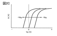
- FIG. 2C is a diagram illustrating Id-Vg characteristics of a transistor.
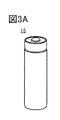
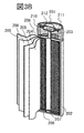
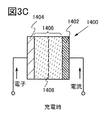
- 3A, 3B, and 3C are a perspective view and a conceptual view showing one embodiment of the present invention.
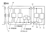
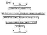
- 4A and 4B are an example of a block diagram and an example of a flowchart illustrating one embodiment of the present invention.
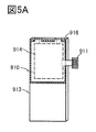
- 5A and 5B are conceptual diagrams showing one embodiment of the present invention.
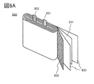
- 6A and 6B are perspective views showing one embodiment of the present invention.
- FIG. 7 is a sectional view showing a configuration example of a semiconductor device.
- FIGS. 8A, 8B, and 8C are cross-sectional views illustrating structural examples of transistors.
- 9A is a top view illustrating a structural example of a transistor
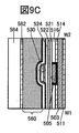
- FIGS. 9B and 9C are cross-sectional views illustrating a structural example of a transistor.
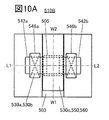
- 10A is a top view illustrating a structural example of a transistor
- FIGS. 10B and 10C are cross-sectional views illustrating a structural example of a transistor.
- 11A is a top view illustrating a structural example of a transistor
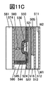
- FIGS. 11B and 11C are cross-sectional views illustrating a structural example of a transistor.
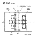
- 12A is a top view illustrating a structural example of a transistor, and FIGS.
- FIGS. 12B and 12C are cross-sectional views illustrating a structural example of a transistor.
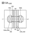
- 13A is a top view illustrating a structural example of a transistor
- FIGS. 13B and 13C are cross-sectional views illustrating a structural example of a transistor.
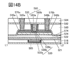
- 14A is a top view illustrating a structural example of a transistor
- FIGS. 14B and 14C are cross-sectional views illustrating a structural example of a transistor.
- 15A is a top view illustrating a structural example of a transistor
- FIG. 15B is a perspective view illustrating a structural example of a transistor.
- 16A and 16B are cross-sectional views illustrating a structural example of a transistor.
- FIG. 17 is a diagram illustrating an example of an electronic device.
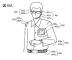
- 18A and 18B are diagrams illustrating examples of electronic devices.
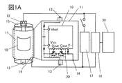
- FIG. 1A is a conceptual diagram of a charging control system for wireless charging in which a charging control circuit 10 formed on a flexible substrate 11 which is a flexible film is mounted on a cylindrical secondary battery 15.
- Vbat is the voltage of the secondary battery
- Vss and V ⁇ are the voltages of the charge control circuit
- Dout and Cout are the output terminals.
- the charging control system includes at least a cylindrical secondary battery 15, a charging control circuit 10, a first switch 20, a charging circuit 16, and an antenna 30.
- the cylindrical secondary battery 15 has a first terminal 12 on the top surface and a second terminal 13 on the bottom surface.
- the first transmission line connected to the first terminal 12 of the cylindrical secondary battery and transmitting the electric power output from the cylindrical secondary battery 15 is electrically connected to the terminal of the charging control circuit via the electrode 18.
- the second transmission line connected to the second terminal 13 of the cylindrical secondary battery is connected via the electrode 19 to the first switch 20 that shuts off the second transmission line.
- FIG. 1A two switching diodes each including a transistor and a diode are connected as a first switch 20 (also referred to as a breaking switch) that cuts off a second transmission line, and an overdischarge, an overcharge, or an overcurrent occurs. It functions as a protection circuit to prevent The first switch 20 controls conduction and interruption operations, and can also be called switching means for switching between supply and interruption.
- the third terminal 14, which is the other terminal of the second transmission path formed on the flexible substrate 11, is connected to the charging circuit 16 and the electronic device 17.
- a third transmission path through which electric power is supplied from the antenna 30 (or the power receiving circuit) to the cylindrical secondary battery 15 via the charging circuit 16 during charging.
- a method in which the charge control circuit 10 is formed over a semiconductor substrate, peeled using a peeling method, and then fixed over the flexible substrate 11 is used.
- a known technique can be used for the peeling method.
- a method in which after the semiconductor substrate is formed, the back surface is polished and then fixed on the flexible substrate 11 may be used.
- a method of fixing the flexible substrate 11 on the flexible substrate 11 after so-called laser cutting which is partially cut by using laser light may be used.
- the charging control circuit 10 may be directly formed on the flexible substrate 11.
- a method of peeling the charge control circuit 10 formed on the glass substrate using a peeling method and then fixing the charge control circuit 10 on the flexible substrate 11 may be used.
- the present invention is not particularly limited to this configuration.
- the second transmission line can be cut off by inputting a signal to the gate of the first switch 20 which cuts off the second transmission line. .. If the second transmission path is cut off, the supply of current from the charging circuit 16 or the supply of current to the electronic device 17 can be stopped. In addition, by holding the signal voltage applied to the gate of the switch 20 which blocks the second transmission path in the memory circuit (including the transistor including an oxide semiconductor), the blocking can be maintained for a long time.
- the output transistor (second switch) of the charging circuit 16 is turned off to shut off the third transmission line. It is possible to stop power transmission by transmitting a signal to stop power transmission from the antenna 30. Therefore, a highly safe charge control system can be obtained.
- FIG. 1B is a process diagram showing a state immediately before the cylindrical secondary battery 15 and the flexible substrate 11 are bonded together, and shows the contact surface side of the flexible substrate 11.
- the barrel portion of the cylindrical secondary battery 15 is applied to the contact surface of the flexible substrate 11 and is rolled, and the flexible substrate 11 is wound and attached in the circumferential direction of the barrel portion.
- the electrodes 18 and 19 are arranged side by side in the Y direction on the flexible substrate 11, but the arrangement is not particularly limited, and one of them may be displaced in the X direction.
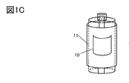
- FIG. 1C The figure after rolling is FIG. 1C.
- An exterior film is attached so as to cover the outer peripheral surface of the body of the cylindrical secondary battery 15. This exterior film is used to protect the metal can for sealing the internal structure of the secondary battery and to insulate it from the metal can.
- the electrode 18 or the electrode 19 is a conductive metal foil, a conductive tape made of a conductive material, or a lead wire, and is known to the terminals of the cylindrical secondary battery 15 by soldering, wire bonding, or the like. Connect by the method.
- the electrode 18 or the electrode 19 is connected to the terminal of the charge control circuit 10 by soldering or wire bonding.
- the charge control circuit 10 and the protection circuit in the curved surface region on the side surface of the cylindrical secondary battery 15.
- the area of the flexible substrate 11 is almost the same as the side surface area of the cylindrical secondary battery (the length in the X direction is 3.14 ⁇ 18 mm).
- Y-direction length is 65 mm) or less.
- the area of the flexible substrate 11 is 3.14 ⁇ 26 mm in the X direction and 65 mm in the Y direction.
- the curved region of the flexible substrate 11 has a radius of curvature of about 9 mm.
- the radius of curvature does not uniformly become about 9 mm due to the influence of the circuit and wiring provided on the flexible substrate 11, and therefore the smallest radius of curvature is the radius of curvature of the surface in this specification and the like.
- the curved surface has a shape having a plurality of curvature centers, it refers to the curvature radius of the curved surface having the smallest curvature radius among the curvature radii at each of the plurality of curvature centers.
- the flexible substrate 11 can be bent within a range of a radius of curvature of 30 mm or more, preferably 9 mm or more.
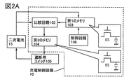
- FIG. 2A An example of a block diagram of a specific circuit of the charge control circuit 10 is shown in FIG. 2A.
- the charge control circuit 10 for the secondary battery 15 includes at least a comparison circuit 102, a first memory 103, a second memory 104, and a control circuit 106.
- the secondary battery 15 and the cutoff switch 105 are shown separately from the charge control circuit 10, but the cutoff switch 105 and the charge control circuit 10 can be formed on the same substrate. ..
- the comparison circuit 102 compares the magnitude relationship of two input voltages and outputs the result.
- the comparison circuit 102 can also be a unipolar circuit using a transistor including an oxide semiconductor in a channel formation region.
- the first memory 103 is an analog memory and stores the analog potential of the offset secondary battery.
- the offset voltage value data of the secondary battery can be created by the parasitic capacitance generated between the gate electrode and the drain electrode by applying a write signal to the gate of the transistor of the first memory 103.
- the first memory 103 includes one transistor including an oxide semiconductor in a channel formation region and a capacitor.
- the first memory 103 can also be called a highly accurate charging voltage monitor circuit.
- the first memory 103 can take advantage of a low leakage current of a transistor including an oxide semiconductor in a channel formation region.
- the second memory 104 has the same element configuration as the first memory 103, and includes one transistor having an oxide semiconductor (OS) in a channel formation region and a capacitor.
- the second memory 104 holds the data of the cutoff switch 105 (first switch).
- the cutoff switch 105 (first switch) is a switch for cutting off the power supply to the power source of the secondary battery in which the abnormality has occurred.
- the circuit configuration of the shutoff switch 105 shown in FIG. 2A can prevent the secondary battery 15 in which an abnormality has occurred from being continuously charged and ignited by overcharging. Further, the charging control circuit 10 turns off the output transistor of the charging circuit to reduce the risk of overcharging.
- FIG. 2A shows an example in which the power supply to the secondary battery 15 is stopped after the abnormality is detected by using the cutoff switch 105 (first switch), but the charging condition is changed or the charging condition is changed according to the number of times of the abnormality detection. Charging may be suspended or a warning may be displayed.
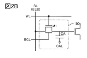
- FIG. 2B is an example of a circuit configuration of the memory cell 100 when the transistor has a back gate.
- the memory cell 100 has a transistor M1 and a capacitor CA.
- the transistor M1 has a front gate (also simply referred to as a “gate”) and a back gate.
- the back gate is arranged so that the gate and the back gate sandwich the channel formation region of the semiconductor layer.
- the names of the gate and the back gate are for convenience, and when one is called a "gate”, the other is called a "back gate”. Therefore, the names of the gate and the back gate can be used interchangeably.
- one of the gate and the back gate is called a "first gate” and the other is called a "second gate”.
- One of the source and the drain of the transistor M1 is electrically connected to one electrode of the capacitor CA, and the other of the source and the drain of the transistor M1 is electrically connected to the bit line BL or the bit line BLB. Is electrically connected to the word line WL, and the back gate of the transistor M1 is electrically connected to the wiring BGL.
- the other electrode of the capacitor CA is connected to the wiring CAL.
- the wiring CAL functions as a wiring for applying a predetermined potential to the other electrode of the capacitor CA. It is preferable to supply a fixed potential such as VSS to the wiring CAL at the time of writing and reading data.
- the wiring BGL functions as a wiring for applying a potential to the back gate of the transistor M1.
- FIG. 2C shows an example of the Id-Vg characteristic which is one of the electric characteristics of the transistor.
- the Id-Vg characteristic shows changes in the drain current (Id) with respect to changes in the gate voltage (Vg).
- the horizontal axis of FIG. 2C represents Vg on a linear scale.
- the vertical axis of FIG. 2C represents Id on a log scale.
- Vbg back gate voltage
- the Id-Vg characteristic shifts in the negative direction of Vg.
- the voltage -Vbg that is a negative bias is supplied to the wiring BGL
- the Id-Vg characteristic is shifted in the plus direction of Vg.
- the shift amount of the Id-Vg characteristic is determined by the magnitude of the voltage supplied to the wiring BGL.
- the threshold voltage of the transistor M1 can be increased or decreased by adjusting the voltage applied to the wiring BGL.
- a potential for making the transistor M1 conductive is supplied to the word line WL to make the transistor M1 conductive, so that the bit line BL or the bit line BLB and one electrode of the capacitor CA. Is electrically connected.
- the leak current of the transistor M1 can be made extremely low. That is, since the written data can be held for a long time by the transistor M1, the frequency of refreshing the memory cell can be reduced. Further, the refresh operation of the memory cell can be made unnecessary. Moreover, since the leak current is very low, analog data can be held in the memory cell.
- the cylindrical secondary battery 15 when power is supplied from the cylindrical secondary battery 15 to the electronic device 17, the cylindrical secondary battery 15 is in a discharged state, and the voltage at the first terminal 12 and the second terminal 13 is increased.
- the charging control circuit 10 monitors behaviors such as current and current and detects an abnormality, the first switch 20 shuts off the second transmission path to stop discharging.
- the electronic device 17 refers to a configuration other than the secondary battery, and the power source for the electronic device 17 is the cylindrical secondary battery 15.
- the electronic device 17 includes a mobile device that can be carried around and carried around.
- the cylindrical secondary battery 15 When the cylindrical secondary battery 15 is wirelessly supplied with electric power to be charged, the cylindrical secondary battery 15 is in a charged state. Behaviors such as voltage and current at the first terminal 12 and the second terminal 13 are monitored by the charge control circuit 10, and when an abnormality is detected, the second transmission path and the third transmission path are shut off. Stop charging.
- the charging circuit 16 refers to a circuit that performs power transmission using a wireless signal.
- the charging circuit 16 may be built in the electronic device 17.
- the electronic device 17 incorporates a rigid board on which a plurality of circuits are mounted, and uses a battery around which a charge control circuit is wound as a power source.
- a block diagram in which the processor 23, the power supply circuit 24, the charging circuit 16, the power receiving circuit 22, and the like are mounted on a rigid substrate is shown in FIG. 4A. It should be noted that the same reference numerals are used for the common parts between FIG. 4A and FIG. 1A.
- the primary coil 31 and the secondary coil (antenna 30) are electrically connected to the terminals of the rigid board as an antenna module.
- FIG. 4B shows an example of the flow of the charge control system in the case where overcharge is detected during one charge of the electronic device 17 in which the charge control circuit 10 is mounted on the secondary battery 15.
- the charge control circuit 10 detects overcharge (S1).
- the charging control circuit 10 turns off the first switch 20 which is a breaking switch, and notifies the charging circuit 16 that overcharging is detected (S2).
- the charging circuit 16 stops charging by turning off the output transistor of the charging circuit 16, and notifies the power receiving circuit 22 of completion of charging (S3).
- the power receiving circuit 22 sends a signal to the power transmission side to stop power transmission (S4).
- the transmission from the primary coil 31 is stopped and the charging is stopped (S5).
- the invention is not particularly limited, and the same flow may be used for preventing overcurrent, detecting an abnormality such as a micro short circuit, and the like.
- the cylindrical secondary battery 15 has a positive electrode cap (battery lid) 201 on the upper surface and battery cans (exterior cans) 202 on the side surfaces and the bottom surface.
- the positive electrode cap and the battery can (exterior can) 202 are insulated by a gasket (insulating packing) 210.
- FIG. 3B is a diagram schematically showing a cross section of the cylindrical secondary battery.
- a battery element in which a strip-shaped positive electrode 204 and a negative electrode 206 are wound with a separator 205 sandwiched therebetween is provided.
- the battery element is wound around the center pin.
- the battery can 202 has one end closed and the other end open.
- a metal such as nickel, aluminum, or titanium having corrosion resistance to an electrolytic solution, an alloy thereof, or an alloy of these and another metal (for example, stainless steel) can be used. . Further, in order to prevent corrosion due to the electrolytic solution, it is preferable to coat with nickel or aluminum.
- the secondary battery includes a positive electrode containing an active material such as lithium cobalt oxide (LiCoO 2 ) and lithium iron phosphate (LiFePO 4 ), a negative electrode made of a carbon material such as graphite capable of inserting and extracting lithium ions, and ethylene. It is composed of a non-aqueous electrolytic solution in which an electrolyte made of a lithium salt such as LiBF 4 or LiPF 6 is dissolved in an organic solvent such as carbonate or diethyl carbonate.
- an active material such as lithium cobalt oxide (LiCoO 2 ) and lithium iron phosphate (LiFePO 4 )
- LiFePO 4 lithium iron phosphate
- a positive electrode terminal (positive electrode current collecting lead) 203 is connected to the positive electrode 204, and a negative electrode terminal (negative electrode current collecting lead) 207 is connected to the negative electrode 206. Both the positive electrode terminal 203 and the negative electrode terminal 207 can use a metal material such as aluminum.
- the positive electrode terminal 203 is resistance-welded to the safety valve mechanism 212, and the negative electrode terminal 207 is resistance-welded to the bottom of the battery can 202.
- the safety valve mechanism 212 is electrically connected to the positive electrode cap 201 via a PTC (Positive Temperature Coefficient) element 211.
- the safety valve mechanism 212 disconnects the electrical connection between the positive electrode cap 201 and the positive electrode 204 when the increase in the internal pressure of the battery exceeds a predetermined threshold value.
- the PTC element 211 is a PTC element whose resistance increases when the temperature rises, and limits the amount of current due to the increase in resistance to prevent abnormal heat generation. Barium titanate (BaTiO 3 ) based semiconductor ceramics or the like can be used for the PTC element.
- a lithium-ion secondary battery using an electrolytic solution has a positive electrode, a negative electrode, a separator, an electrolytic solution, and an outer package.
- the anode (anode) and the cathode (cathode) are switched by charging and discharging, and the oxidation reaction and the reduction reaction are switched. Therefore, the electrode with a high reaction potential is called the positive electrode, and the reaction potential is higher. The electrode with a low value is called the negative electrode. Therefore, in the present specification, the positive electrode is a “positive electrode” or “a positive electrode” or a “positive electrode” during charging, discharging, reverse pulse current, or charging current.
- the positive electrode is referred to as a "positive electrode” and the negative electrode is referred to as a "negative electrode” or a “negative electrode”.
- anode (anode)” and “cathode (cathode)” related to the oxidation reaction and the reduction reaction are used, the charging time and the discharging time are reversed, which may cause confusion. Therefore, the terms anode (anode) and cathode (cathode) are not used in this specification. If the terms anode (anode) and cathode (cathode) are used, indicate whether they are charging or discharging and also indicate whether they correspond to the positive electrode (positive electrode) or the negative electrode (negative electrode). To do.
- a charger is connected to the two terminals shown in FIG. 3C to charge the storage battery 1400.
- 1406 is an electrolytic solution and 1408 is a separator.
- the potential difference between the electrodes increases.
- the direction of the current flowing from the external terminal of the storage battery 1400 toward the positive electrode 1402, in the storage battery 1400 from the positive electrode 1402 toward the negative electrode 1404, and from the negative electrode toward the external terminal of the storage battery 1400. Is the positive direction. That is, the direction in which the charging current flows is the direction of the current.
- an example of a lithium ion secondary battery is shown; however, the material is not limited to a lithium ion secondary battery, and a material containing an element A, an element X, and oxygen is used as a positive electrode material of the secondary battery.
- the element A is preferably one or more selected from Group 1 elements and Group 2 elements.
- the Group 1 element for example, an alkali metal such as lithium, sodium, or potassium can be used.
- the Group 2 element for example, calcium, beryllium, magnesium, or the like can be used.
- the element X for example, one or more selected from a metal element, silicon and phosphorus can be used.
- the element X is preferably one or more selected from cobalt, nickel, manganese, iron, and vanadium.
- lithium cobalt composite oxide (LiCoO 2 ) and lithium iron phosphate (LiFePO 4 ) can be given.
- the negative electrode has a negative electrode active material layer and a negative electrode current collector. Further, the negative electrode active material layer may have a conductive additive and a binder.
- an element capable of performing a charge / discharge reaction by an alloying / dealloying reaction with lithium can be used.
- a material containing at least one of silicon, tin, gallium, aluminum, germanium, lead, antimony, bismuth, silver, zinc, cadmium, indium, and the like can be used.
- Such an element has a larger capacity than carbon, and particularly silicon has a high theoretical capacity of 4200 mAh / g.
- the secondary battery preferably has a separator.
- the separator for example, fibers including cellulose such as paper, non-woven fabric, glass fiber, ceramics, or nylon (polyamide), vinylon (polyvinyl alcohol fiber), polyester, acryl, polyolefin, synthetic fiber using polyurethane, etc. It is possible to use those formed in.
- FIG. 5A is a diagram showing an external view of a battery pack having a flat secondary battery 913, a charge control circuit 914, and a connection terminal 911.
- the charge control circuit 914 is formed or fixed on the flexible substrate 910.
- the charge control circuit 914 detects an abnormality such as a micro short circuit. Further, it may have a function as a protection circuit that protects the secondary battery 913 from overcharge, overdischarge, and overcurrent.
- the charge control circuit 914 the charge control circuit 10 described in Embodiment 1 can be used. Since the same circuit configuration and the like can be used, detailed description will be omitted here.
- an antenna and a power receiving circuit may be provided as illustrated in FIG. 4A.
- the secondary battery 913 can be charged in a contactless manner by using an antenna.
- the antenna is not limited to the coil shape, and may be, for example, a linear shape or a plate shape.
- an antenna such as a planar antenna, an aperture antenna, a traveling wave antenna, an EH antenna, a magnetic field antenna, or a dielectric antenna may be used.
- the antenna has a function of performing data communication with an external device, for example.
- a response system that can be used between the battery pack and another device such as NFC can be applied.
- connection terminal 911 is electrically connected to the terminals 951 and 952 included in the secondary battery 913 through the charge control circuit 914.
- a plurality of connection terminals 911 may be provided and each of the plurality of connection terminals 911 may serve as a control signal input terminal, a power supply terminal, or the like.
- the battery pack has an insulating sheet layer 916 between the charge control circuit 914 and the secondary battery 913.
- the insulating sheet layer 916 has a function of preventing a short circuit due to the secondary battery 913, for example.
- an organic resin film or an adhesive sheet can be used as the insulating sheet layer 916.
- the structure of the wound body 950 disposed inside the secondary battery 913 is shown in FIG. 6A.
- the wound body 950 includes a negative electrode 931, a positive electrode 932, and a separator 933.
- the wound body 950 is a wound body in which a negative electrode 931 and a positive electrode 932 are laminated with a separator 933 sandwiched therebetween and the laminated sheet is wound. Note that a plurality of stacked layers of the negative electrode 931, the positive electrode 932, and the separator 933 may be further stacked.
- the negative electrode 931 is connected to the connection terminal 911 shown in FIG. 5 through one of the terminal 951 and the terminal 952.
- the positive electrode 932 is connected to the connection terminal 911 shown in FIG. 5 through the other of the terminal 951 and the terminal 952.
- the wound body 950 shown in FIG. 6A is impregnated with the electrolytic solution inside the exterior body.
- a case made of metal is used as the exterior body.
- a film may be used as the exterior body, and in that case, a charge control circuit formed on a flexible substrate may be provided on the film.
- a secondary battery 913 illustrated in FIG. 6B includes a wound body 950 in which a terminal 951 and a terminal 952 are provided inside a housing 930.
- the wound body 950 is impregnated with the electrolytic solution inside the housing 930.
- the terminal 952 is in contact with the housing 930, and the terminal 951 is not in contact with the housing 930 by using an insulating material or the like.
- the housing 930 is illustrated separately for convenience, but in reality, the wound body 950 is covered with the housing 930, and the terminals 951 and 952 extend outside the housing 930.
- Existence A metal material (for example, aluminum) or a resin material can be used for the housing 930.
- an insulating material such as a metal material or an organic resin can be used.
- FIG. 5A shows an example in which the insulating sheet layer 916 is provided on the surface of the housing and the flexible substrate is fixed with the surface on which the charge control circuit is provided inside, but the invention is not particularly limited, and charging may be performed.
- the terminals 951 and 952 may be connected with the surface on which the control circuit is formed facing outward. However, in that case, the connection part will be exposed and there is a risk of electrostatic breakdown or short circuit, so be careful when assembling.
- the secondary battery 913 can have high safety.
- This embodiment mode can be freely combined with Embodiment Mode 1.
- OS transistor is a thin film transistor and can be formed over a separation layer provided over a glass substrate or can be stacked over a single crystal silicon substrate.
- Embodiment 1 is an example in which a flexible substrate provided with a charge control circuit is attached to a curved surface of a secondary battery
- an OS transistor formed over a peeling layer provided over a glass substrate can be formed by a known method. It is fixed to the flexible substrate by a peeling method.
- the second embodiment is an example in which the charge control circuit is attached to the flat surface of the secondary battery
- the OS transistor is formed over the single crystal silicon substrate, for example, the back surface of the single crystal silicon substrate is polished.
- the thin film is fixed to a flexible substrate.
- the OS transistor may be separated from the single crystal silicon substrate by a hydrogen ion implantation separation method and fixed to the flexible substrate.
- the semiconductor device illustrated in FIG. 7 includes a transistor 300, a transistor 500, and a capacitor 600.
- 8A is a cross-sectional view of the transistor 500 in the channel length direction
- FIG. 8B is a cross-sectional view of the transistor 500 in the channel width direction
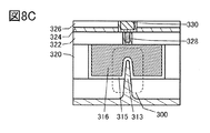
- FIG. 8C is a cross-sectional view of the transistor 300 in the channel width direction.
- the transistor 500 is a transistor including a metal oxide in a channel formation region (OS transistor).
- the transistor 500 has features that a high voltage can be applied between a source and a drain, off current is unlikely to increase even in a high temperature environment, and a ratio of on current to off current is high even in a high temperature environment.
- the mobile device can be a highly safe semiconductor device.
- the semiconductor device described in this embodiment includes a transistor 300, a transistor 500, and a capacitor 600 as illustrated in FIG. 7.
- the transistor 500 is provided above the transistor 300
- the capacitor 600 is provided above the transistor 300 and the transistor 500.
- the transistor 300 is provided over the substrate 311, and includes a conductor 316, an insulator 315, a semiconductor region 313 formed of part of the substrate 311, a low resistance region 314a functioning as a source region or a drain region, and a low resistance region 314b.
- a conductor 316 includes a conductor 316, an insulator 315, a semiconductor region 313 formed of part of the substrate 311, a low resistance region 314a functioning as a source region or a drain region, and a low resistance region 314b.
- the transistor 300 As shown in FIG. 8C, in the transistor 300, the upper surface of the semiconductor region 313 and the side surface in the channel width direction are covered with the conductor 316 with the insulator 315 interposed therebetween. As described above, when the transistor 300 is a Fin type, the effective channel width is increased, so that the on-state characteristics of the transistor 300 can be improved. Further, since the electric field contribution of the gate electrode can be increased, the off characteristics of the transistor 300 can be improved.
- the transistor 300 may be either a p-channel type or an n-channel type.
- a region of the semiconductor region 313 in which a channel is formed, a region in the vicinity thereof, a low-resistance region 314a serving as a source region or a drain region, a low-resistance region 314b, or the like preferably contains a semiconductor such as a silicon-based semiconductor. It preferably includes crystalline silicon. Alternatively, a material including Ge (germanium), SiGe (silicon germanium), GaAs (gallium arsenide), GaAlAs (gallium aluminum arsenide), or the like may be used. A configuration may be used in which silicon is used, in which the effective mass is controlled by applying stress to the crystal lattice and changing the lattice spacing. Alternatively, the transistor 300 may be a HEMT (High Electron Mobility Transistor) by using GaAs and GaAlAs.
- HEMT High Electron Mobility Transistor
- the low-resistance region 314a and the low-resistance region 314b impart an n-type conductivity imparting element such as arsenic or phosphorus, or a p-type conductivity imparting boron, in addition to the semiconductor material applied to the semiconductor region 313. Including the element to do.
- the conductor 316 functioning as a gate electrode is a semiconductor material such as silicon, a metal material, or an alloy containing an element imparting n-type conductivity such as arsenic or phosphorus, or an element imparting p-type conductivity such as boron. Materials or conductive materials such as metal oxide materials can be used.
- Vth of the transistor can be adjusted by changing the material of the conductor.
- a material such as titanium nitride or tantalum nitride for the conductor.
- a metal material such as tungsten or aluminum as a laminate for the conductor, and it is particularly preferable to use tungsten in terms of heat resistance.
- transistor 300 illustrated in FIGS. 7A and 7B is an example, and the structure is not limited thereto; an appropriate transistor may be used depending on a circuit structure or a driving method.
- An insulator 320, an insulator 322, an insulator 324, and an insulator 326 are sequentially stacked to cover the transistor 300.
- the insulator 320, the insulator 322, the insulator 324, and the insulator 326 for example, silicon oxide, silicon oxynitride, silicon nitride oxide, silicon nitride, aluminum oxide, aluminum oxynitride, aluminum nitride oxide, aluminum nitride, or the like is used. Good.
- the insulator 322 may have a function as a planarization film which planarizes a step generated by the transistor 300 or the like provided below the insulator 322.
- the upper surface of the insulator 322 may be flattened by a flattening treatment using a chemical mechanical polishing (CMP) method or the like in order to improve flatness.
- CMP chemical mechanical polishing
- the insulator 324 it is preferable to use a film having a barrier property such that hydrogen and impurities do not diffuse from the substrate 311, the transistor 300, or the like to a region where the transistor 500 is provided.
- a film having a barrier property against hydrogen for example, silicon nitride formed by a CVD method can be used.
- silicon nitride formed by a CVD method when hydrogen is diffused into a semiconductor element including an oxide semiconductor, such as the transistor 500, characteristics of the semiconductor element may be deteriorated in some cases. Therefore, it is preferable to use a film which suppresses diffusion of hydrogen between the transistor 500 and the transistor 300.
- the film that suppresses hydrogen diffusion is a film in which the amount of released hydrogen is small.
- the desorption amount of hydrogen can be analyzed using, for example, the temperature programmed desorption gas analysis (TDS analysis) method.
- TDS analysis the desorption amount of hydrogen in the insulator 324 is calculated by converting the desorption amount converted into hydrogen atoms into the area of the insulator 324 when the surface temperature of the film is in the range of 50 ° C to 500 ° C. Therefore, it may be 10 ⁇ 10 15 atoms / cm 2 or less, preferably 5 ⁇ 10 15 atoms / cm 2 or less.
- the insulator 326 preferably has a lower dielectric constant than the insulator 324.
- the dielectric constant of the insulator 326 is preferably less than 4, and more preferably less than 3.
- the relative dielectric constant of the insulator 326 is preferably 0.7 times or less, and more preferably 0.6 times or less that of the insulator 324.
- the insulator 320, the insulator 322, the insulator 324, and the insulator 326 are embedded with a conductor 328 which is connected to the capacitor 600 or the transistor 500, a conductor 330, and the like.
- the conductor 328 and the conductor 330 have a function as a plug or a wiring.
- a conductor having a function as a plug or a wiring may have a plurality of structures collectively given the same reference numeral. In this specification and the like, the wiring and the plug connected to the wiring may be integrated. That is, part of the conductor may function as a wiring, and part of the conductor may function as a plug.
- a conductive material such as a metal material, an alloy material, a metal nitride material, or a metal oxide material is formed in a single layer or stacked layers.
- a high melting point material such as tungsten or molybdenum, which has both heat resistance and conductivity, and it is preferable to use tungsten.
- tungsten it is preferably formed of a low resistance conductive material such as aluminum or copper. Wiring resistance can be reduced by using a low-resistance conductive material.
- a wiring layer may be provided over the insulator 326 and the conductor 330.
- an insulator 350, an insulator 352, and an insulator 354 are sequentially stacked and provided.
- a conductor 356 is formed over the insulator 350, the insulator 352, and the insulator 354.
- the conductor 356 has a function as a plug connected to the transistor 300 or a wiring. Note that the conductor 356 can be provided using a material similar to that of the conductor 328 and the conductor 330.
- the insulator 350 is preferably an insulator having a barrier property against hydrogen similarly to the insulator 324.
- the conductor 356 preferably contains a conductor having a barrier property against hydrogen.
- a conductor having a hydrogen barrier property is formed in an opening portion of the insulator 350 having a hydrogen barrier property.
- tantalum nitride or the like is preferably used as the conductor having a barrier property against hydrogen.
- tantalum nitride or the like is preferably used as the conductor having a barrier property against hydrogen.
- tantalum nitride and tungsten having high conductivity diffusion of hydrogen from the transistor 300 can be suppressed while maintaining conductivity as a wiring.
- the tantalum nitride layer having a barrier property against hydrogen be in contact with the insulator 350 having a barrier property against hydrogen.
- a wiring layer may be provided over the insulator 354 and the conductor 356.
- an insulator 360, an insulator 362, and an insulator 364 are sequentially stacked and provided.
- a conductor 366 is formed over the insulator 360, the insulator 362, and the insulator 364.
- the conductor 366 has a function as a plug or a wiring. Note that the conductor 366 can be provided using a material similar to that of the conductor 328 and the conductor 330.
- the insulator 360 like the insulator 324, an insulator having a barrier property against hydrogen is preferably used.
- the conductor 366 preferably contains a conductor having a barrier property against hydrogen.
- a conductor having a hydrogen barrier property is formed in the opening of the insulator 360 having a hydrogen barrier property.
- a wiring layer may be provided over the insulator 364 and the conductor 366.
- an insulator 370, an insulator 372, and an insulator 374 are sequentially stacked and provided.
- a conductor 376 is formed over the insulator 370, the insulator 372, and the insulator 374.
- the conductor 376 has a function as a plug or a wiring. Note that the conductor 376 can be provided using a material similar to that of the conductor 328 and the conductor 330.
- the conductor 376 preferably includes a conductor having a barrier property against hydrogen.
- a conductor having a hydrogen barrier property is formed in the opening of the insulator 370 having a hydrogen barrier property.
- a wiring layer may be provided over the insulator 374 and the conductor 376.
- an insulator 380, an insulator 382, and an insulator 384 are sequentially stacked and provided.
- a conductor 386 is formed over the insulator 380, the insulator 382, and the insulator 384.
- the conductor 386 has a function as a plug or a wiring. Note that the conductor 386 can be provided using a material similar to that of the conductor 328 and the conductor 330.
- the insulator 380 is preferably an insulator having a barrier property against hydrogen, like the insulator 324.
- the conductor 386 preferably contains a conductor having a barrier property against hydrogen.
- a conductor having a barrier property against hydrogen is formed in the opening portion of the insulator 380 having a barrier property against hydrogen.
- the semiconductor device has been described above, the semiconductor device according to this embodiment It is not limited to this.
- the number of wiring layers similar to the wiring layer including the conductor 356 may be three or less, or the number of wiring layers similar to the wiring layer including the conductor 356 may be five or more.
- An insulator 510, an insulator 512, an insulator 514, and an insulator 516 are sequentially stacked over the insulator 384.
- Any of the insulator 510, the insulator 512, the insulator 514, and the insulator 516 is preferably formed using a substance having a barrier property against oxygen and hydrogen.
- insulator 510 and the insulator 514 for example, a film having a barrier property in which hydrogen and impurities do not diffuse from the substrate 311 or a region where the transistor 300 is provided to a region where the transistor 500 is provided is used. Is preferred. Therefore, a material similar to that of the insulator 324 can be used.
- silicon nitride formed by a CVD method can be used as an example of a film having a barrier property against hydrogen.
- silicon nitride formed by a CVD method when hydrogen is diffused into a semiconductor element including an oxide semiconductor, such as the transistor 500, characteristics of the semiconductor element may be deteriorated in some cases. Therefore, it is preferable to use a film which suppresses diffusion of hydrogen between the transistor 500 and the transistor 300.
- the film that suppresses hydrogen diffusion is a film in which the amount of released hydrogen is small.
- a metal oxide such as aluminum oxide, hafnium oxide, or tantalum oxide is preferably used for the insulator 510 and the insulator 514.
- aluminum oxide has a high blocking effect of not permeating oxygen and impurities such as hydrogen and moisture, which cause fluctuations in electrical characteristics of a transistor, through the film. Therefore, aluminum oxide can prevent impurities such as hydrogen and moisture from entering the transistor 500 during and after the manufacturing process of the transistor. Further, release of oxygen from the oxide included in the transistor 500 can be suppressed. Therefore, it is suitable to be used as a protective film for the transistor 500.
- the same material as that of the insulator 320 can be used for the insulator 512 and the insulator 516. Further, by using a material having a relatively low dielectric constant as the interlayer film, it is possible to reduce the parasitic capacitance generated between the wirings.
- a silicon oxide film, a silicon oxynitride film, or the like can be used as the insulator 512 and the insulator 516.
- a conductor 518, a conductor (conductor 503) included in the transistor 500, and the like are embedded in the insulator 510, the insulator 512, the insulator 514, and the insulator 516.
- the conductor 518 has a function of a plug connected to the capacitor 600 or the transistor 300, or a wiring.
- the conductor 518 can be provided using a material similar to that of the conductor 328 and the conductor 330.
- the conductor 510 in a region which is in contact with the insulator 510 and the insulator 514 is preferably a conductor having a barrier property against oxygen, hydrogen, and water.
- the transistor 300 and the transistor 500 can be separated by a layer having a barrier property against oxygen, hydrogen, and water, and diffusion of hydrogen from the transistor 300 to the transistor 500 can be suppressed.
- the transistor 500 is provided above the insulator 516.
- a transistor 500 includes a conductor 503 which is arranged so as to be embedded in an insulator 512 and an insulator 516, and an insulator 520 which is arranged over the insulator 516 and the conductor 503.
- an insulator 544 is preferably provided between the insulator 580 and the oxide 530a, the oxide 530b, the conductor 542a, and the conductor 542b.
- the conductor 560 includes a conductor 560a provided inside the insulator 550 and a conductor 560b provided so as to be embedded inside the conductor 560a. It is preferable to have.
- an insulator 574 is preferably provided over the insulator 580, the conductor 560, and the insulator 550.
- the oxide 530a, the oxide 530b, and the oxide 530c may be collectively referred to as the oxide 530.
- the conductor 542a and the conductor 542b may be collectively referred to as a conductor 542.
- the transistor 500 has a structure in which three layers of the oxide 530a, the oxide 530b, and the oxide 530c are stacked in the region where the channel is formed and in the vicinity thereof, the present invention is not limited to this. Not a thing. For example, a single layer of the oxide 530b, a two-layer structure of the oxide 530b and the oxide 530a, a two-layer structure of the oxide 530b and the oxide 530c, or a stacked structure of four or more layers may be provided. Further, in the transistor 500, the conductor 560 is shown as a stacked structure of two layers, but the present invention is not limited to this. For example, the conductor 560 may have a single-layer structure or a stacked structure including three or more layers. Further, the transistor 500 illustrated in FIGS. 7, 8A, and 8B is an example, and the structure thereof is not limited, and an appropriate transistor may be used depending on a circuit structure or a driving method.
- the conductor 560 functions as a gate electrode of the transistor, and the conductors 542a and 542b function as a source electrode or a drain electrode, respectively.
- the conductor 560 is formed so as to be embedded in the opening of the insulator 580 and the region between the conductor 542a and the conductor 542b.
- the arrangement of the conductor 560, the conductor 542a, and the conductor 542b is selected in a self-aligned manner with respect to the opening of the insulator 580. That is, in the transistor 500, the gate electrode can be arranged between the source electrode and the drain electrode in a self-aligned manner. Therefore, the conductor 560 can be formed without providing a positioning margin, so that the area occupied by the transistor 500 can be reduced. As a result, miniaturization and high integration of the semiconductor device can be achieved.
- the conductor 560 is formed in a region between the conductor 542a and the conductor 542b in a self-aligned manner, the conductor 560 does not have a region overlapping with the conductor 542a or the conductor 542b. Accordingly, the parasitic capacitance formed between the conductor 560 and the conductors 542a and 542b can be reduced. Therefore, the switching speed of the transistor 500 can be improved and high frequency characteristics can be provided.
- the conductor 560 may function as a first gate (also referred to as a top gate) electrode.
- the conductor 503 may function as a second gate (also referred to as a bottom gate) electrode.
- the Vth of the transistor 500 can be controlled by changing the potential applied to the conductor 503 independently of the potential applied to the conductor 560 without being interlocked.
- Vth of the transistor 500 can be higher than 0 V and off-state current can be reduced. Therefore, applying a negative potential to the conductor 503 can reduce the drain current when the potential applied to the conductor 560 is 0 V, as compared to the case where no potential is applied.
- the conductor 503 is arranged so as to overlap with the oxide 530 and the conductor 560. Thus, when a potential is applied to the conductor 560 and the conductor 503, the electric field generated from the conductor 560 and the electric field generated from the conductor 503 are connected to cover a channel formation region formed in the oxide 530.
- a structure of a transistor which electrically surrounds a channel formation region by an electric field of a first gate electrode and a second gate electrode is referred to as a surrounded channel (S-channel) structure.
- the side surface and the periphery of the oxide 530 which is in contact with the conductors 542a and 542b functioning as a source electrode and a drain electrode are i-type as in the channel formation region. It has characteristics.
- the side surface and the periphery of the oxide 530 which are in contact with the conductors 542a and 542b are in contact with the insulator 544 and thus can be i-type as in the channel formation region.
- I-form can be treated as the same as high-purity intrinsic, which will be described later.
- the S-channel structure disclosed in this specification and the like is different from the Fin structure and the planar structure.
- the conductor 503 has a structure similar to that of the conductor 518.
- the conductor 503a is formed in contact with the inner walls of the openings of the insulator 514 and the insulator 516, and the conductor 503b is formed further inside.
- the insulator 520, the insulator 522, the insulator 524, and the insulator 550 have a function as a gate insulating film.
- the insulator 524 which is in contact with the oxide 530, an insulator containing more oxygen than that in the stoichiometric composition is preferably used. That is, it is preferable that the insulator 524 be formed with an excess oxygen region. By providing such an insulator containing excess oxygen in contact with the oxide 530, oxygen vacancies in the oxide 530 can be reduced and the reliability of the transistor 500 can be improved.
- an oxide material in which part of oxygen is released by heating is preferably used as the insulator having an excess oxygen region.
- the oxide that desorbs oxygen by heating means that the amount of desorbed oxygen in terms of oxygen atoms is 1.0 ⁇ 10 18 atoms / cm 3 or more, preferably 1 or more by TDS (Thermal Desorption Spectroscopy) analysis.
- the oxide film has a density of 0.0 ⁇ 10 19 atoms / cm 3 or more, more preferably 2.0 ⁇ 10 19 atoms / cm 3 or more, or 3.0 ⁇ 10 20 atoms / cm 3 or more.
- the surface temperature of the film during the TDS analysis is preferably 100 ° C. or higher and 700 ° C. or lower, or 100 ° C. or higher and 400 ° C. or lower.
- the insulator 522 preferably has a function of suppressing diffusion of oxygen (eg, oxygen atoms, oxygen molecules) (the oxygen is less likely to permeate).
- oxygen eg, oxygen atoms, oxygen molecules
- the insulator 522 has a function of suppressing diffusion of oxygen and impurities, oxygen included in the oxide 530 does not diffuse to the insulator 520 side, which is preferable. Further, the conductor 503 can be prevented from reacting with the insulator 524 and the oxygen contained in the oxide 530.
- the insulator 522 is, for example, so-called high such as aluminum oxide, hafnium oxide, tantalum oxide, zirconium oxide, lead zirconate titanate (PZT), strontium titanate (SrTiO 3 ) or (Ba, Sr) TiO 3 (BST). It is preferable to use an insulator containing a -k material in a single layer or a laminated layer. As miniaturization and higher integration of transistors progress, problems such as leakage current may occur due to thinning of the gate insulating film. By using a high-k material for the insulator functioning as a gate insulating film, it is possible to reduce the gate potential during transistor operation while maintaining the physical film thickness.
- an insulator containing an oxide of one or both of aluminum and hafnium which is an insulating material having a function of suppressing diffusion of impurities, oxygen, and the like (oxygen does not easily pass through) is preferably used.
- the insulator containing one or both oxides of aluminum and hafnium it is preferable to use aluminum oxide, hafnium oxide, an oxide containing aluminum and hafnium (hafnium aluminate), or the like.
- the insulator 522 is formed using such a material, the insulator 522 suppresses release of oxygen from the oxide 530 and mixture of impurities such as hydrogen from the peripheral portion of the transistor 500 into the oxide 530. Functions as a layer.
- aluminum oxide, bismuth oxide, germanium oxide, niobium oxide, silicon oxide, titanium oxide, tungsten oxide, yttrium oxide, or zirconium oxide may be added to these insulators.
- these insulators may be nitrided. Silicon oxide, silicon oxynitride, or silicon nitride may be stacked over the above insulator and used.
- the insulator 520 is preferably thermally stable.
- silicon oxide and silicon oxynitride are preferable because they are thermally stable.
- an insulator of a high-k material with silicon oxide or silicon oxynitride, an insulator 520 having a stacked structure which is thermally stable and has a high relative dielectric constant can be obtained.
- the insulator 520, the insulator 522, and the insulator 524 may have a stacked structure of two or more layers.
- the laminated structure is not limited to the same material, and may be a laminated structure made of different materials.
- a metal oxide which functions as an oxide semiconductor is preferably used.
- the oxide 530 an In-M-Zn oxide (the element M is aluminum, gallium, yttrium, copper, vanadium, beryllium, boron, titanium, iron, nickel, germanium, zirconium, molybdenum, lanthanum, cerium, neodymium). , Or one or more selected from hafnium, tantalum, tungsten, magnesium, or the like).
- an In—Ga oxide or an In—Zn oxide may be used.
- a metal oxide having a low carrier density is preferably used.
- the concentration of impurities in the metal oxide may be lowered and the density of defect states may be lowered.
- low impurity concentration and low defect level density are referred to as high-purity intrinsic or substantially high-purity intrinsic.
- the impurities in the metal oxide include, for example, hydrogen, nitrogen, alkali metals, alkaline earth metals, iron, nickel, silicon and the like.
- hydrogen contained in a metal oxide reacts with oxygen bonded to a metal atom to be water, which may cause oxygen vacancies in the metal oxide. If the channel formation region in the metal oxide contains oxygen vacancies, the transistor might have normally-on characteristics. Further, a defect in which hydrogen is contained in an oxygen vacancy may function as a donor and an electron which is a carrier may be generated. Further, part of hydrogen may be bonded to oxygen which is bonded to a metal atom to generate an electron which is a carrier. Therefore, a transistor including a metal oxide containing a large amount of hydrogen is likely to have normally-on characteristics.
- a defect in which hydrogen is contained in an oxygen vacancy can function as a metal oxide donor.
- the carrier density may be evaluated instead of the donor concentration. Therefore, in this specification and the like, a carrier density that assumes a state where an electric field is not applied is sometimes used as a parameter of a metal oxide, instead of a donor concentration. That is, the “carrier density” described in this specification and the like can be called the “donor concentration” in some cases.
- the hydrogen concentration obtained by secondary ion mass spectrometry is less than 1 ⁇ 10 20 atoms / cm 3 , preferably 1 ⁇ 10 19 atoms / cm 3. It is less than 3 , more preferably less than 5 ⁇ 10 18 atoms / cm 3 , and even more preferably less than 1 ⁇ 10 18 atoms / cm 3 .
- the carrier density of the metal oxide in the channel formation region is preferably 1 ⁇ 10 18 cm ⁇ 3 or less and less than 1 ⁇ 10 17 cm ⁇ 3. Is more preferable, less than 1 ⁇ 10 16 cm ⁇ 3 is more preferable, less than 1 ⁇ 10 13 cm ⁇ 3 is still more preferable, and less than 1 ⁇ 10 12 cm ⁇ 3 is further preferable.
- the lower limit of the carrier density of the metal oxide in the channel formation region is not particularly limited, but can be set to, for example, 1 ⁇ 10 ⁇ 9 cm ⁇ 3 .
- the conductor 542 (the conductor 542a and the conductor 542b) and the oxide 530 are in contact with each other, so that oxygen in the oxide 530 diffuses into the conductor 542,
- the conductor 542 may be oxidized. Oxidation of the conductor 542 is likely to reduce the conductivity of the conductor 542. Note that diffusion of oxygen in the oxide 530 to the conductor 542 can be restated as absorption of oxygen in the oxide 530 by the conductor 542.
- oxygen in the oxide 530 diffuses into the conductor 542 (the conductor 542a and the conductor 542b), so that the conductor 542a and the oxide 530b are separated from each other and the conductor 542b and the oxide 530b are separated from each other.
- Different layers may be formed between them. Since the different layer contains more oxygen than the conductor 542, it is estimated that the different layer has an insulating property.
- the three-layer structure of the conductor 542, the different layer, and the oxide 530b can be regarded as a three-layer structure including a metal-insulator-semiconductor and a MIS (Metal-Insulator-Semiconductor) structure. In some cases, it may be referred to as a diode junction structure mainly including the MIS structure.
- the different layer is not limited to being formed between the conductor 542 and the oxide 530b; for example, when the different layer is formed between the conductor 542 and the oxide 530c, or It may be formed between the body 542 and the oxide 530b and between the conductor 542 and the oxide 530c.
- a metal oxide having a bandgap of 2 eV or more, preferably 2.5 eV or more is preferably used.
- the oxide 530 includes the oxide 530a below the oxide 530b, so that diffusion of impurities into the oxide 530b from a structure formed below the oxide 530a can be suppressed. Further, by including the oxide 530c over the oxide 530b, diffusion of impurities from the structure formed above the oxide 530c into the oxide 530b can be suppressed.
- the oxide 530 preferably has a stacked structure of a plurality of oxide layers in which the atomic ratio of each metal atom is different.
- the atomic ratio of the element M in the constituent elements is higher than the atomic ratio of the element M in the constituent elements in the metal oxide used for the oxide 530b.
- the atomic ratio of the element M to In is preferably higher than the atomic ratio of the element M to In in the metal oxide used for the oxide 530b.
- the atomic ratio of In to the element M is preferably higher than the atomic ratio of In to the element M in the metal oxide used for the oxide 530a.
- a metal oxide that can be used for the oxide 530a or the oxide 530b can be used.
- the energy of the bottom of the conduction band of the oxide 530a and the oxide 530c is preferably higher than the energy of the bottom of the conduction band of the oxide 530b.
- the electron affinity of the oxide 530a and the oxide 530c be smaller than the electron affinity of the oxide 530b.
- the energy level at the bottom of the conduction band changes gently at the junction of the oxide 530a, the oxide 530b, and the oxide 530c.
- the energy levels at the bottoms of the conduction bands at the junctions of the oxide 530a, the oxide 530b, and the oxide 530c are continuously changed or continuously joined.
- the oxide 530a and the oxide 530b, and the oxide 530b and the oxide 530c have a common element other than oxygen (as a main component), so that a mixed layer with low density of defect states is formed.
- the oxide 530b is an In—Ga—Zn oxide
- an In—Ga—Zn oxide, a Ga—Zn oxide, gallium oxide, or the like may be used as the oxide 530a and the oxide 530c.
- the main path of carriers is the oxide 530b.
- the oxide 530a and the oxide 530c having the above structure, the density of defect states in the interface between the oxide 530a and the oxide 530b and the interface between the oxide 530b and the oxide 530c can be reduced. Therefore, the influence of interface scattering on carrier conduction is reduced and the transistor 500 can obtain high on-state current.
- the conductor 542 (the conductor 542a and the conductor 542b) which functions as a source electrode and a drain electrode is provided over the oxide 530b.
- the conductor 542 aluminum, chromium, copper, silver, gold, platinum, tantalum, nickel, titanium, molybdenum, tungsten, hafnium, vanadium, niobium, manganese, magnesium, zirconium, beryllium, indium, ruthenium, iridium, strontium, It is preferable to use a metal element selected from lanthanum, an alloy containing the above metal element as a component, an alloy in which the above metal elements are combined, or the like.
- tantalum nitride, titanium nitride, tungsten, nitride containing titanium and aluminum, nitride containing tantalum and aluminum, ruthenium oxide, ruthenium nitride, oxide containing strontium and ruthenium, oxide containing lanthanum and nickel, or the like is used.
- tantalum nitride, titanium nitride, nitride containing titanium and aluminum, nitride containing tantalum and aluminum, ruthenium oxide, ruthenium nitride, oxide containing strontium and ruthenium, and oxide containing lanthanum and nickel are difficult to oxidize.
- a conductive material or a material that maintains conductivity even when absorbing oxygen is preferable.
- a region 543 (a region 543a and a region 543b) may be formed as a low-resistance region at the interface between the oxide 530 and the conductor 542 and in the vicinity thereof.
- the region 543a functions as one of the source region and the drain region
- the region 543b functions as the other of the source region and the drain region.
- a channel formation region is formed in a region between the region 543a and the region 543b.
- the oxygen concentration in the region 543 may be reduced. Further, a metal compound layer containing a metal contained in the conductor 542 and a component of the oxide 530 may be formed in the region 543. In such a case, the carrier density of the region 543 increases, and the region 543 becomes a low resistance region.
- the insulator 544 is provided so as to cover the conductor 542 and suppresses oxidation of the conductor 542. At this time, the insulator 544 may be provided so as to cover a side surface of the oxide 530 and be in contact with the insulator 524.
- a metal oxide containing one kind or two or more kinds selected from hafnium, aluminum, gallium, yttrium, zirconium, tungsten, titanium, tantalum, nickel, germanium, magnesium, or the like can be used. it can.
- the insulator 544 aluminum oxide, hafnium oxide, an oxide containing hafnium (a hafnium aluminate), or the like, which is an insulator containing an oxide of one or both of aluminum and hafnium.
- hafnium aluminate has higher heat resistance than a hafnium oxide film. Therefore, crystallization is less likely to occur in heat treatment in a later step, which is preferable.
- the insulator 544 is not an essential component when the conductor 542 is a material having oxidation resistance or when the conductivity does not significantly decrease even when oxygen is absorbed. It may be appropriately designed depending on the desired transistor characteristics.
- the insulator 550 functions as a gate insulating film.
- the insulator 550 is preferably arranged in contact with the inside (top surface and side surface) of the oxide 530c.
- the insulator 550 is preferably formed using an insulator from which oxygen is released by heating.
- the amount of released oxygen in terms of oxygen atoms is 1.0 ⁇ 10 18 atoms / cm 3 or more, preferably 1.0 ⁇ 10 19 atoms / cm 3 or more, more preferably 2
- the surface temperature of the film during the TDS analysis is preferably 100 ° C. or higher and 700 ° C. or lower.
- silicon oxide containing excess oxygen, silicon oxynitride, silicon nitride oxide, silicon nitride, silicon oxide containing fluorine, silicon oxide containing carbon, silicon oxide containing carbon and nitrogen, and vacancy Silicon oxide can be used.
- silicon oxide and silicon oxynitride are preferable because they are stable to heat.
- oxygen is effectively supplied from the insulator 550 to the channel formation region of the oxide 530b through the oxide 530c. Can be supplied.
- the concentration of impurities such as water or hydrogen in the insulator 550 is preferably reduced.
- the thickness of the insulator 550 is preferably 1 nm or more and 20 nm or less.
- a metal oxide may be provided between the insulator 550 and the conductor 560 in order to efficiently supply the excess oxygen included in the insulator 550 to the oxide 530.
- the metal oxide preferably suppresses oxygen diffusion from the insulator 550 to the conductor 560.
- diffusion of excess oxygen from the insulator 550 to the conductor 560 is suppressed. That is, a decrease in the amount of excess oxygen supplied to the oxide 530 can be suppressed.
- oxidation of the conductor 560 due to excess oxygen can be suppressed.
- a material that can be used for the insulator 544 may be used.
- the conductor 560 functioning as the first gate electrode has a two-layer structure in FIGS. 8A and 8B, it may have a single-layer structure or a stacked structure of three or more layers.
- the conductor 560a has a function of suppressing diffusion of impurities such as hydrogen atoms, hydrogen molecules, water molecules, nitrogen atoms, nitrogen molecules, nitric oxide molecules (N 2 O, NO, NO 2, etc.), and copper atoms. It is preferable to use materials. Alternatively, it is preferable to use a conductive material having a function of suppressing diffusion of oxygen (eg, at least one of oxygen atoms and oxygen molecules). Since the conductor 560a has a function of suppressing diffusion of oxygen, oxygen contained in the insulator 550 can prevent oxidation of the conductor 560b and decrease in conductivity.
- the conductive material having a function of suppressing diffusion of oxygen for example, tantalum, tantalum nitride, ruthenium, ruthenium oxide, or the like is preferably used.
- the conductor 560b also functions as a wiring, it is preferable to use a conductor having high conductivity.
- a conductor having high conductivity For example, a conductive material containing tungsten, copper, or aluminum as its main component can be used.
- the conductor 560b may have a stacked structure, for example, a stacked structure of titanium or titanium nitride and the above conductive material.
- the insulator 580 is provided over the conductor 542 with the insulator 544 interposed therebetween.
- the insulator 580 preferably has an excess oxygen region.
- silicon oxide and silicon oxynitride are preferable because they are thermally stable.
- silicon oxide and silicon oxide having vacancies are preferable because an excess oxygen region can be easily formed in a later step.
- the insulator 580 preferably has an excess oxygen region. By providing the insulator 580 from which oxygen is released by heating in contact with the oxide 530c, oxygen in the insulator 580 can be efficiently supplied to the oxide 530 through the oxide 530c. Note that the concentration of impurities such as water or hydrogen in the insulator 580 is preferably reduced.
- the opening of the insulator 580 is formed so as to overlap with a region between the conductor 542a and the conductor 542b. Accordingly, the conductor 560 is formed so as to be embedded in the opening of the insulator 580 and the region between the conductor 542a and the conductor 542b.
- the conductor 560 When miniaturizing a semiconductor device, it is required to shorten the gate length, but it is necessary to prevent the conductivity of the conductor 560 from being lowered. Therefore, if the thickness of the conductor 560 is increased, the conductor 560 can have a shape with a high aspect ratio. In this embodiment mode, the conductor 560 is provided so as to be embedded in the opening of the insulator 580; therefore, even if the conductor 560 has a high aspect ratio, the conductor 560 can be formed without being destroyed during the process. You can
- the insulator 574 is preferably provided in contact with the top surface of the insulator 580, the top surface of the conductor 560, and the top surface of the insulator 550.
- an excess oxygen region can be provided in the insulator 550 and the insulator 580. Accordingly, oxygen can be supplied into the oxide 530 from the excess oxygen region.
- insulator 574 a metal oxide containing one kind or two or more kinds selected from hafnium, aluminum, gallium, yttrium, zirconium, tungsten, titanium, tantalum, nickel, germanium, magnesium, or the like is used. You can
- aluminum oxide has a high barrier property and can suppress diffusion of hydrogen and nitrogen even in a thin film of 0.5 nm to 3.0 nm. Therefore, the aluminum oxide film formed by a sputtering method can have a function as a barrier film against impurities such as hydrogen as well as an oxygen supply source.
- an insulator 581 which functions as an interlayer film is preferably provided over the insulator 574.
- the insulator 581 preferably has a reduced concentration of impurities such as water or hydrogen in the film.
- the conductors 540a and 540b are provided in the openings formed in the insulator 581, the insulator 574, the insulator 580, and the insulator 544.
- the conductor 540a and the conductor 540b are provided to face each other with the conductor 560 interposed therebetween.
- the conductors 540a and 540b have the same configurations as the conductors 546 and 548 described later.
- An insulator 582 is provided over the insulator 581.
- the insulator 582 it is preferable to use a substance having a barrier property against oxygen and hydrogen. Therefore, a material similar to that of the insulator 514 can be used for the insulator 582.
- the insulator 582 is preferably formed using a metal oxide such as aluminum oxide, hafnium oxide, or tantalum oxide.
- aluminum oxide has a high blocking effect of not permeating oxygen and impurities such as hydrogen and moisture, which cause fluctuations in electrical characteristics of a transistor, through the film. Therefore, aluminum oxide can prevent impurities such as hydrogen and moisture from entering the transistor 500 during and after the manufacturing process of the transistor. Further, release of oxygen from the oxide included in the transistor 500 can be suppressed. Therefore, it is suitable to be used as a protective film for the transistor 500.
- an insulator 586 is provided over the insulator 582.
- a material similar to that of the insulator 320 can be used.
- a material having a relatively low dielectric constant as the interlayer film it is possible to reduce the parasitic capacitance generated between the wirings.
- a silicon oxide film, a silicon oxynitride film, or the like can be used as the insulator 586.
- the insulator 520, the insulator 522, the insulator 524, the insulator 544, the insulator 580, the insulator 574, the insulator 581, the insulator 582, and the insulator 586 include the conductor 546, the conductor 548, and the like. Is embedded.
- the conductor 546 and the conductor 548 have a function of a plug connected to the capacitor 600, the transistor 500, or the transistor 300, or a wiring.
- the conductor 546 and the conductor 548 can be provided using a material similar to that of the conductor 328 and the conductor 330.
- the capacitor 600 is provided above the transistor 500.
- the capacitor 600 includes a conductor 610, a conductor 620, and an insulator 630.
- the conductor 612 may be provided over the conductor 546 and the conductor 548.
- the conductor 612 has a function as a plug connected to the transistor 500 or a wiring.
- the conductor 610 has a function as an electrode of the capacitor 600. Note that the conductor 612 and the conductor 610 can be formed at the same time.
- a metal film containing an element selected from molybdenum, titanium, tantalum, tungsten, aluminum, copper, chromium, neodymium, and scandium, or a metal nitride film containing the above element as a component (Tantalum nitride film, titanium nitride film, molybdenum nitride film, tungsten nitride film) or the like can be used.
- indium tin oxide, indium oxide containing tungsten oxide, indium zinc oxide containing tungsten oxide, indium oxide containing titanium oxide, indium tin oxide containing titanium oxide, indium zinc oxide, or silicon oxide is added.
- a conductive material such as indium tin oxide described above can also be applied.
- the conductor 612 and the conductor 610 are illustrated as a single-layer structure; however, the structure is not limited thereto and a stacked structure of two or more layers may be used.
- a conductor having a barrier property and a conductor having high adhesion to the conductor having high conductivity may be formed between the conductor having barrier property and the conductor having high conductivity.
- the conductor 620 is provided so as to overlap with the conductor 610 with the insulator 630 interposed therebetween.
- the conductor 620 can be formed using a conductive material such as a metal material, an alloy material, or a metal oxide material. It is preferable to use a high melting point material such as tungsten or molybdenum that has both heat resistance and conductivity, and it is particularly preferable to use tungsten.
- a low resistance metal material such as Cu (copper) or Al (aluminum) may be used.
- An insulator 650 is provided over the conductor 620 and the insulator 630.
- the insulator 650 can be provided using a material similar to that of the insulator 320. Further, the insulator 650 may function as a flattening film that covers the uneven shape below the insulator 650.
- a transistor including an oxide semiconductor variation in electric characteristics can be suppressed and reliability can be improved.
- a transistor including an oxide semiconductor with high on-state current can be provided.
- a transistor including an oxide semiconductor with low off-state current can be provided.
- a semiconductor device with reduced power consumption can be provided.
- a semiconductor device including a transistor including an oxide semiconductor can be miniaturized or highly integrated.
- transistor 500 in the semiconductor device described in this embodiment is not limited to the above structure.
- structural examples that can be used for the transistor 500 will be described.
- FIG. 9A is a top view of the transistor 510A.
- 9B is a cross-sectional view of a portion indicated by alternate long and short dash line L1-L2 in FIG. 9A.
- FIG. 9C is a sectional view of a portion indicated by alternate long and short dash line W1-W2 in FIG. 9A.
- some elements are omitted for clarity.
- 9A, 9B, and 9C show a transistor 510A, an insulator 511, an insulator 512, an insulator 514, an insulator 516, an insulator 580, an insulator 582, and an insulator 584 which function as interlayer films.
- a conductor 546 (a conductor 546a and a conductor 546b) which is electrically connected to the transistor 510A and functions as a contact plug and a conductor 503 which functions as a wiring are illustrated.
- the transistor 510A includes a conductor 560 (a conductor 560a and a conductor 560b) which functions as a first gate electrode, a conductor 505 (a conductor 505a, and a conductor 505b) which functions as a second gate electrode.
- An insulator 550 that functions as a first gate insulating film, an insulator 521 that functions as a second gate insulating film, an insulator 522, and an insulator 524, and an oxide 530 (oxidized with a region where a channel is formed).
- Object 530a, oxide 530b, and oxide 530c Object 530a, oxide 530b, and oxide 530c
- a conductor 542a which functions as one of a source and a drain
- a conductor 542b which functions as the other of a source and a drain
- an insulator 574 an insulator
- the oxide 530c, the insulator 550, and the conductor 560 are provided in the opening provided in the insulator 580 with the insulator 574 interposed therebetween.
- the oxide 530c, the insulator 550, and the conductor 560 are provided between the conductor 542a and the conductor 542b.
- the insulator 511 and the insulator 512 function as an interlayer film.
- interlayer film examples include silicon oxide, silicon oxynitride, silicon nitride oxide, aluminum oxide, hafnium oxide, tantalum oxide, zirconium oxide, lead zirconate titanate (PZT), strontium titanate (SrTiO 3 ) or (Ba, Sr).
- An insulator such as TiO 3 (BST) can be used as a single layer or a stacked layer.
- aluminum oxide, bismuth oxide, germanium oxide, niobium oxide, silicon oxide, titanium oxide, tungsten oxide, yttrium oxide, or zirconium oxide may be added to these insulators.
- these insulators may be nitrided. Silicon oxide, silicon oxynitride, or silicon nitride may be stacked over the above insulator and used.
- the insulator 511 preferably functions as a barrier film which suppresses impurities such as water or hydrogen from entering the transistor 510A from the substrate side. Therefore, the insulator 511 is preferably formed using an insulating material having a function of suppressing diffusion of impurities such as hydrogen atoms, hydrogen molecules, water molecules, and copper atoms (the above impurities are less likely to pass through). Alternatively, it is preferable to use an insulating material having a function of suppressing diffusion of oxygen (eg, at least one of oxygen atoms and oxygen molecules) (the above oxygen is less likely to permeate). Further, for example, aluminum oxide, silicon nitride, or the like may be used as the insulator 511. With this structure, impurities such as hydrogen and water can be suppressed from diffusing from the substrate side of the insulator 511 to the transistor 510A side.
- impurities such as hydrogen and water can be suppressed from diffusing from the substrate side of the insulator 511 to the transistor 510A side
- the insulator 512 preferably has a lower dielectric constant than the insulator 511.
- a material having a low dielectric constant as the interlayer film, it is possible to reduce the parasitic capacitance generated between the wirings.
- the conductor 503 is formed so as to be embedded in the insulator 512.
- the height of the upper surface of the conductor 503 and the height of the upper surface of the insulator 512 can be approximately the same.
- the conductor 503 is illustrated as having a single layer structure, but the present invention is not limited to this.
- the conductor 503 may have a multilayer film structure including two or more layers.
- the conductor 503 is preferably formed using a conductive material containing tungsten, copper, or aluminum as its main component and having high conductivity.
- the conductor 560 may function as a first gate (also referred to as a top gate) electrode. Further, the conductor 505 may function as a second gate (also referred to as a bottom gate) electrode. In that case, by changing the potential applied to the conductor 505 independently of the potential applied to the conductor 560, the threshold voltage of the transistor 510A can be controlled. In particular, by applying a negative potential to the conductor 505, the threshold voltage of the transistor 510A can be higher than 0 V and the off-state current can be reduced. Therefore, applying a negative potential to the conductor 505 can reduce the drain current when the potential applied to the conductor 560 is 0 V, as compared to the case where no potential is applied.
- an electric field generated from the conductor 560 and an electric field generated from the conductor 505. can cover the channel formation region formed in the oxide 530.
- the channel formation region can be electrically surrounded by the electric field of the conductor 560 having a function as the first gate electrode and the electric field of the conductor 505 having a function as the second gate electrode. That is, similarly to the transistor 500 described above, it has a surrounded channel (S-channel) structure.
- the insulator 514 and the insulator 516 function as an interlayer film similarly to the insulator 511 or the insulator 512.
- the insulator 514 preferably functions as a barrier film which suppresses impurities such as water or hydrogen from entering the transistor 510A from the substrate side. With such a structure, diffusion of impurities such as hydrogen and water from the substrate side of the insulator 514 to the transistor 510A side can be suppressed.
- the insulator 516 preferably has a lower dielectric constant than the insulator 514. By using a material having a low dielectric constant as the interlayer film, it is possible to reduce the parasitic capacitance generated between the wirings.
- the conductor 505 functioning as the second gate, the conductor 505a is formed in contact with the inner walls of the openings of the insulator 514 and the insulator 516, and the conductor 505b is further formed inside.
- the heights of the top surfaces of the conductors 505a and 505b and the top surface of the insulator 516 can be approximately the same.
- the transistor 510A has a structure in which the conductors 505a and 505b are stacked; however, the present invention is not limited to this.
- the conductor 505 may have a single-layer structure or a stacked structure including three or more layers.
- the conductor 505a is preferably formed using a conductive material having a function of suppressing diffusion of impurities such as hydrogen atoms, hydrogen molecules, water molecules, and copper atoms (the above impurities are less likely to penetrate).
- a conductive material having a function of suppressing diffusion of oxygen eg, at least one of oxygen atoms and oxygen molecules
- the function of suppressing the diffusion of impurities or oxygen is the function of suppressing the diffusion of any one or all of the impurities or oxygen.
- the conductor 505a has a function of suppressing diffusion of oxygen, so that the conductor 505b can be prevented from being oxidized and being reduced in conductivity.
- the conductor 505b is preferably formed using a conductive material having high conductivity, which contains tungsten, copper, or aluminum as its main component. In that case, the conductor 503 is not necessarily provided.
- the conductor 505b is illustrated as a single layer, it may have a laminated structure, for example, a laminate of titanium or titanium nitride and the above conductive material.
- the insulator 521, the insulator 522, and the insulator 524 have a function as a second gate insulating film.
- the insulator 522 preferably has a barrier property.
- the insulator 522 having a barrier function functions as a layer which suppresses entry of impurities such as hydrogen from the peripheral portion of the transistor 510A into the transistor 510A.
- the insulator 522 includes, for example, aluminum oxide, hafnium oxide, an oxide containing aluminum and hafnium (hafnium aluminate), tantalum oxide, zirconium oxide, lead zirconate titanate (PZT), strontium titanate (SrTiO 3 ) or ( It is preferable to use an insulator containing a so-called high-k material such as Ba, Sr) TiO 3 (BST) in a single layer or a laminated layer. As miniaturization and higher integration of transistors progress, problems such as leakage current may occur due to thinning of the gate insulating film. By using a high-k material for the insulator functioning as a gate insulating film, it is possible to reduce the gate potential during transistor operation while maintaining the physical film thickness.
- the insulator 521 is preferably thermally stable.
- silicon oxide and silicon oxynitride are preferable because they are thermally stable.
- an insulator made of a high-k material with silicon oxide or silicon oxynitride, an insulator 521 having a stacked structure which is thermally stable and has a high relative dielectric constant can be obtained.
- FIG. 9 illustrates a stacked structure of three layers as the second gate insulating film, but a single layer or a stacked structure of two or more layers may be used.
- the laminated structure is not limited to the same material, and may be a laminated structure made of different materials.
- the oxide 530 having a region functioning as a channel formation region includes the oxide 530a, the oxide 530b over the oxide 530a, and the oxide 530c over the oxide 530b.
- the oxide 530a under the oxide 530b diffusion of impurities from the structure formed below the oxide 530a into the oxide 530b can be suppressed.
- the oxide 530c over the oxide 530b diffusion of impurities from the structure formed above the oxide 530c into the oxide 530b can be suppressed.
- an oxide semiconductor which is one of the above metal oxides can be used.
- the oxide 530c is preferably provided in the opening provided in the insulator 580 with the insulator 574 provided therebetween.
- the insulator 574 has a barrier property, diffusion of impurities from the insulator 580 into the oxide 530 can be suppressed.
- One of the conductors 542 functions as a source electrode and the other functions as a drain electrode.
- a metal such as aluminum, titanium, chromium, nickel, copper, yttrium, zirconium, molybdenum, silver, tantalum, or tungsten, or an alloy containing any of these as a main component can be used.
- a metal nitride film such as tantalum nitride is preferable because it has a barrier property against hydrogen or oxygen and has high oxidation resistance.
- the conductor 542 has a single-layer structure in FIG. 9, it may have a stacked-layer structure of two or more layers.
- a tantalum nitride film and a tungsten film may be stacked.
- a titanium film and an aluminum film may be stacked.
- a two-layer structure in which an aluminum film is stacked over a tungsten film a two-layer structure in which a copper film is stacked over a copper-magnesium-aluminum alloy film, a two-layer structure in which a copper film is stacked over a titanium film, and a tungsten film is formed over the tungsten film.
- a two-layer structure in which copper films are laminated may be used.
- a titanium film or a titanium nitride film a three-layer structure in which an aluminum film or a copper film is stacked over the titanium film or the titanium nitride film, and a titanium film or a titanium nitride film is formed thereover, a molybdenum film, or
- a molybdenum nitride film and an aluminum film or a copper film are stacked over the molybdenum film or the molybdenum nitride film, and a molybdenum film or a molybdenum nitride film is formed thereover.
- a transparent conductive material containing indium oxide, tin oxide, or zinc oxide may be used.
- a barrier layer may be provided over the conductor 542.
- a substance having a barrier property against oxygen or hydrogen is preferably used. With this structure, the conductor 542 can be prevented from being oxidized when the insulator 574 is formed.
- a metal oxide can be used for the barrier layer.
- an insulating film having a barrier property against oxygen or hydrogen such as aluminum oxide, hafnium oxide, or gallium oxide.
- silicon nitride formed by a CVD method may be used.
- the material selection range for the conductor 542 can be widened.
- the conductor 542 a material such as tungsten or aluminum which has low oxidation resistance and high conductivity can be used. Further, for example, a conductor which can be easily formed into a film or processed can be used.
- the insulator 550 functions as a first gate insulating film.
- the insulator 550 is preferably provided in the opening provided in the insulator 580 with the oxide 530c and the insulator 574 provided therebetween.
- the insulator 550 may have a stacked-layer structure like the second gate insulating film.
- the insulator functioning as a gate insulating film has a laminated structure of a high-k material and a thermally stable material, so that the gate potential during transistor operation can be reduced while maintaining the physical film thickness. Becomes Further, it is possible to obtain a laminated structure that is thermally stable and has a high relative dielectric constant.
- the conductor 560 functioning as the first gate electrode has a conductor 560a and a conductor 560b over the conductor 560a.
- the conductor 560a is preferably formed using a conductive material having a function of suppressing diffusion of impurities such as hydrogen atoms, hydrogen molecules, water molecules, and copper atoms.
- a conductive material having a function of suppressing diffusion of oxygen eg, at least one of oxygen atoms and oxygen molecules).
- the conductor 560a has a function of suppressing diffusion of oxygen, the material selectivity of the conductor 560b can be improved. That is, by having the conductor 560a, oxidation of the conductor 560b can be suppressed and the conductivity can be prevented from being lowered.
- a conductive material having a function of suppressing diffusion of oxygen for example, tantalum, tantalum nitride, ruthenium, ruthenium oxide, or the like is preferably used.
- the conductor 560a an oxide semiconductor which can be used as the oxide 530 can be used. In that case, by forming a film of the conductor 560b by a sputtering method, the electric resistance value of the conductor 560a can be reduced and the conductor can be formed. This can be called an OC (Oxide Conductor) electrode.
- the conductor 560b functions as a wiring, it is preferable to use a conductor having high conductivity.
- a conductor having high conductivity For example, a conductive material containing tungsten, copper, or aluminum as its main component can be used.
- the conductor 560b may have a stacked structure, for example, a stack of titanium or titanium nitride and the above conductive material.
- An insulator 574 is provided between the insulator 580 and the transistor 510A.
- an insulating material having a function of suppressing diffusion of impurities such as water or hydrogen and oxygen is preferable.
- impurities such as water or hydrogen and oxygen
- metal oxide such as magnesium oxide, gallium oxide, germanium oxide, yttrium oxide, zirconium oxide, lanthanum oxide, neodymium oxide, or tantalum oxide, silicon nitride oxide, or silicon nitride can be used.
- impurities such as water and hydrogen included in the insulator 580 can be suppressed from diffusing into the oxide 530b through the oxide 530c and the insulator 550.
- oxidation of the conductor 560 due to excess oxygen in the insulator 580 can be suppressed.
- the insulator 580, the insulator 582, and the insulator 584 function as an interlayer film.
- the insulator 582 preferably functions as a barrier insulating film which suppresses impurities such as water or hydrogen from entering the transistor 510A from the outside.
- the insulator 580 and the insulator 584 preferably have a lower dielectric constant than that of the insulator 582.
- the interlayer film By using a material having a low dielectric constant as the interlayer film, it is possible to reduce the parasitic capacitance generated between the wirings.
- the transistor 510A may be electrically connected to another structure through a plug or a wiring such as the insulator 580, the insulator 582, and the conductor 546 embedded in the insulator 584.
- a conductive material such as a metal material, an alloy material, a metal nitride material, or a metal oxide material can be used as a single layer or a stacked layer similarly to the conductor 505.
- a high melting point material such as tungsten or molybdenum that has both heat resistance and conductivity.
- a low resistance conductive material such as aluminum or copper. Wiring resistance can be reduced by using a low-resistance conductive material.
- the conductor 546 a stacked structure of tantalum nitride or the like, which has a barrier property against hydrogen and oxygen, and tungsten, which has high conductivity, is used, so that the conductivity of the wiring is maintained. The diffusion of impurities from the outside can be suppressed.
- a semiconductor device including a transistor including an oxide semiconductor with high on-state current can be provided.
- a semiconductor device including a transistor including an oxide semiconductor with low off-state current can be provided.
- FIG. 10A is a top view of the transistor 510B.
- 10B is a cross-sectional view of a portion indicated by alternate long and short dash line L1-L2 in FIG. 10A.
- FIG. 10C is a sectional view of a portion indicated by alternate long and short dash line W1-W2 in FIG. 10A.
- some elements are omitted for the sake of clarity.
- the transistor 510B is a modification of the transistor 510A. Therefore, in order to prevent repetition of description, points different from the transistor 510A are mainly described.
- the transistor 510B has a region where the conductor 542 (the conductor 542a and the conductor 542b) and the oxide 530c, the insulator 550, and the conductor 560 overlap with each other. With such a structure, a transistor with high on-state current can be provided. In addition, a transistor with high controllability can be provided.
- the conductor 560 functioning as the first gate electrode has a conductor 560a and a conductor 560b over the conductor 560a.
- the conductor 560a is preferably formed using a conductive material having a function of suppressing diffusion of impurities such as hydrogen atoms, hydrogen molecules, water molecules, and copper atoms.
- a conductive material having a function of suppressing diffusion of oxygen eg, at least one of oxygen atoms and oxygen molecules).
- the conductor 560a has a function of suppressing diffusion of oxygen, the material selectivity of the conductor 560b can be improved. That is, by having the conductor 560a, oxidation of the conductor 560b can be suppressed and the conductivity can be prevented from being lowered.
- the insulator 574 is preferably provided so as to cover the top surface and the side surface of the conductor 560, the side surface of the insulator 550, and the side surface of the oxide 530c.
- the insulator 574 may be formed using an insulating material having a function of suppressing diffusion of impurities such as water or hydrogen and oxygen.
- impurities such as water or hydrogen and oxygen.
- metal oxide such as magnesium oxide, gallium oxide, germanium oxide, yttrium oxide, zirconium oxide, lanthanum oxide, neodymium oxide, or tantalum oxide, silicon nitride oxide, or silicon nitride can be used.
- oxidation of the conductor 560 can be suppressed. Further, with the insulator 574, impurities such as water and hydrogen included in the insulator 580 can be suppressed from diffusing into the transistor 510B.
- the insulator 576 having a barrier property may be provided between the conductor 546 and the insulator 580.
- oxygen in the insulator 580 can be prevented from reacting with the conductor 546 and oxidizing the conductor 546.
- the insulator 576 having a barrier property it is possible to widen the selection range of the material of the conductor used for the plug and the wiring.
- a semiconductor device with low power consumption can be provided by using a metal material having high conductivity while having a property of absorbing oxygen for the conductor 546.
- a material such as tungsten or aluminum which has low oxidation resistance but high conductivity can be used.
- a conductor which can be easily formed into a film or processed can be used.
- FIG. 11A is a top view of the transistor 510C.
- 11B is a cross-sectional view of a portion indicated by alternate long and short dash line L1-L2 in FIG. 11A.
- FIG. 11C is a sectional view of a portion indicated by alternate long and short dash line W1-W2 in FIG. 11A.
- some elements are omitted for the sake of clarity.
- the transistor 510C is a modification of the transistor 510A. Therefore, in order to prevent repetition of description, points different from the transistor 510A are mainly described.
- the conductor 547a is provided between the conductor 542a and the oxide 530b
- the conductor 547b is provided between the conductor 542b and the oxide 530b.
- the conductor 542a extends over the top surface of the conductor 547a (conductor 547b) and the side surface on the conductor 560 side and has a region in contact with the top surface of the oxide 530b.
- the conductor 547 a conductor that can be used for the conductor 542 may be used.
- the thickness of the conductor 547 is preferably at least larger than that of the conductor 542.
- the transistor 510C in FIG. 11 can bring the conductor 542 closer to the conductor 560 than the transistor 510A.
- the conductor 560 can overlap with the end of the conductor 542a and the end of the conductor 542b. Accordingly, the substantial channel length of the transistor 510C can be shortened, and the on-current and frequency characteristics can be improved.
- the conductor 547a (conductor 547b) is preferably provided so as to overlap with the conductor 542a (conductor 542b).
- the conductor 547a (conductor 547b) functions as a stopper and the oxide 530b is overetched in etching for forming an opening in which the conductor 546a (conductor 546b) is embedded. Can be prevented.
- the transistor 510C illustrated in FIG. 11 may have a structure in which the insulator 545 is provided in contact with the insulator 544.
- the insulator 544 preferably functions as a barrier insulating film which suppresses impurities such as water or hydrogen and excess oxygen from entering the transistor 510C from the insulator 580 side.
- an insulator that can be used for the insulator 544 can be used.
- a nitride insulator such as aluminum nitride, aluminum titanium nitride, titanium nitride, silicon nitride, or silicon nitride oxide may be used.
- the conductor 505 may have a single-layer structure unlike the transistor 510A illustrated in FIG.
- an insulating film to be the insulator 516 is formed over the patterned conductor 505, and the upper portion of the insulating film is removed by a CMP method or the like until the upper surface of the conductor 505 is exposed.
- the top surface of the conductor 505 be flat.
- the average surface roughness (Ra) of the top surface of the conductor 505 may be 1 nm or less, preferably 0.5 nm or less, more preferably 0.3 nm or less. Accordingly, the flatness of the insulating layer formed over the conductor 505 can be improved and the crystallinity of the oxide 530b and the oxide 530c can be improved.
- FIG. 12A is a top view of the transistor 510D.
- FIG. 12B is a sectional view of a portion indicated by alternate long and short dash line L1-L2 in FIG. 12A.
- FIG. 12C is a sectional view of a portion indicated by alternate long and short dash line W1-W2 in FIG. 12A.
- some elements are omitted for the sake of clarity.
- the transistor 510D is a modification of the above transistor. Therefore, in order to prevent the description from being repeated, differences from the above transistor will be mainly described.
- the conductor 503 is not provided and the conductor 505 having a function as the second gate is also functioned as a wiring.
- the insulator 550 is provided over the oxide 530c, and the metal oxide 552 is provided over the insulator 550.
- the conductor 560 is provided over the metal oxide 552, and the insulator 570 is provided over the conductor 560.
- the insulator 571 is provided over the insulator 570.
- the metal oxide 552 preferably has a function of suppressing oxygen diffusion.
- the metal oxide 552 which suppresses diffusion of oxygen between the insulator 550 and the conductor 560, diffusion of oxygen into the conductor 560 is suppressed. That is, a decrease in the amount of oxygen supplied to the oxide 530 can be suppressed. In addition, oxidation of the conductor 560 due to oxygen can be suppressed.
- the metal oxide 552 may have a function as a part of the first gate.
- an oxide semiconductor that can be used as the oxide 530 can be used as the metal oxide 552.
- the conductor 560 by forming the conductor 560 by a sputtering method, the electric resistance value of the metal oxide 552 can be reduced and the conductive layer (the OC electrode described above) can be formed.
- the metal oxide 552 may have a function as a part of the gate insulating film. Therefore, when silicon oxide, silicon oxynitride, or the like is used for the insulator 550, the metal oxide 552 is preferably a high-k material which has a high relative dielectric constant. With this laminated structure, a laminated structure that is stable to heat and has a high relative dielectric constant can be obtained. Therefore, it is possible to reduce the gate potential applied during transistor operation while maintaining the physical film thickness. Further, the equivalent oxide film thickness (EOT) of the insulating layer functioning as the gate insulating film can be reduced.
- EOT equivalent oxide film thickness
- the metal oxide 552 is shown as a single layer in the transistor 510D, a stacked structure of two or more layers may be used. For example, a metal oxide functioning as part of the gate electrode and a metal oxide functioning as part of the gate insulating film may be stacked.
- the on-state current of the transistor 510D can be improved without reducing the influence of the electric field from the conductor 560.
- the distance between the conductor 560 and the oxide 530 is kept by the physical thickness of the insulator 550 and the metal oxide 552, so that Leakage current with the oxide 530 can be suppressed. Therefore, by providing a laminated structure of the insulator 550 and the metal oxide 552, the physical distance between the conductor 560 and the oxide 530 and the electric field strength applied from the conductor 560 to the oxide 530 are reduced. It can be easily adjusted appropriately.
- the oxide semiconductor can be used as the metal oxide 552.
- a metal oxide containing one kind or two or more kinds selected from hafnium, aluminum, gallium, yttrium, zirconium, tungsten, titanium, tantalum, nickel, germanium, magnesium, or the like can be used.
- hafnium oxide an oxide containing aluminum and hafnium (hafnium aluminate), which is an insulator containing an oxide of one or both of aluminum and hafnium.
- hafnium aluminate has higher heat resistance than a hafnium oxide film. Therefore, crystallization is less likely to occur in heat treatment in a later step, which is preferable.
- the metal oxide 552 is not an essential component. It may be appropriately designed depending on the desired transistor characteristics.
- an insulating material having a function of suppressing permeation of impurities such as water or hydrogen and oxygen is preferably used.
- impurities such as water or hydrogen and oxygen
- the insulator 571 functions as a hard mask.
- the side surface of the conductor 560 is substantially vertical, specifically, the angle formed by the side surface of the conductor 560 and the substrate surface is 75 degrees or more and 100 degrees or less, It is preferably 80 degrees or more and 95 degrees or less.
- the insulator 571 may also serve as a barrier layer by using an insulating material having a function of suppressing permeation of impurities such as water or hydrogen and oxygen. In that case, the insulator 570 may not be provided.
- the insulator 571 As a hard mask and selectively removing a part of the insulator 570, the conductor 560, the metal oxide 552, the insulator 550, and the oxide 530c, these side surfaces are approximately aligned. In addition, part of the surface of the oxide 530b can be exposed.
- the transistor 510D has a region 531a and a region 531b in a part of the exposed surface of the oxide 530b.
- One of the region 531a and the region 531b functions as a source region and the other functions as a drain region.
- the regions 531a and 531b are formed by, for example, an ion implantation method, an ion doping method, a plasma immersion ion implantation method, a plasma treatment, or the like, and an impurity element such as phosphorus or boron is introduced into the exposed surface of the oxide 530b. It can be realized. Note that in this embodiment and the like, an “impurity element” refers to an element other than a main component element.
- a metal film is formed after exposing a part of the surface of the oxide 530b, and then heat treatment is performed, so that an element contained in the metal film is diffused into the oxide 530b to form a region 531a and a region 531b. You can also do it.
- the regions 531a and 531b may be referred to as “impurity regions” or "low resistance regions”.
- the regions 531a and 531b can be formed in a self-aligned manner. Therefore, the region 531a and / or the region 531b does not overlap with the conductor 560, so that parasitic capacitance can be reduced. Further, no offset region is formed between the channel formation region and the source / drain region (region 531a or region 531b).
- a self-aligned manner self-alignment
- an increase in on-current, a reduction in threshold voltage, an improvement in operating frequency, etc. can be realized.
- an offset region may be provided between the channel formation region and the source / drain region in order to further reduce the off-state current.
- the offset region is a region having a high electric resistivity and is a region in which the above-mentioned impurity element is not introduced.
- the offset region can be formed by introducing the above-described impurity element after forming the insulator 575.
- the insulator 575 also functions as a mask similarly to the insulator 571 and the like. Therefore, an impurity element is not introduced into a region of the oxide 530b which overlaps with the insulator 575, so that the electric resistivity of the region can be kept high.
- the transistor 510D includes the insulator 570, the conductor 560, the metal oxide 552, the insulator 550, and the insulator 575 on a side surface of the oxide 530c.
- the insulator 575 is preferably an insulator having a low relative dielectric constant.
- silicon oxide, silicon oxynitride, silicon nitride oxide, silicon nitride, silicon oxide added with fluorine, silicon oxide added with carbon, silicon oxide added with carbon and nitrogen, silicon oxide having holes, or resin Preferably.
- silicon oxide, silicon oxynitride, silicon nitride oxide, or silicon oxide having holes for the insulator 575 because an excess oxygen region can be easily formed in the insulator 575 in a later step.
- silicon oxide and silicon oxynitride are preferable because they are thermally stable.
- the insulator 575 preferably has a function of diffusing oxygen.
- the transistor 510D includes the insulator 575 and the insulator 574 over the oxide 530.
- the insulator 574 is preferably formed by a sputtering method. By using the sputtering method, an insulator containing few impurities such as water or hydrogen can be formed. For example, aluminum oxide is preferably used as the insulator 574.
- an oxide film formed by a sputtering method may extract hydrogen from a structure to be formed. Therefore, the insulator 574 absorbs hydrogen and water from the oxide 530 and the insulator 575, whereby the hydrogen concentration of the oxide 530 and the insulator 575 can be reduced.
- FIG. 13A is a top view of the transistor 510E.
- FIG. 13B is a sectional view of a portion indicated by alternate long and short dash line L1-L2 in FIG.
- FIG. 13C is a sectional view of a portion indicated by alternate long and short dash line W1-W2 in FIG. 13A. Note that in the top view of FIG. 13A, some elements are omitted for clarity.
- the transistor 510E is a modification of the above transistor. Therefore, in order to prevent the description from being repeated, differences from the above transistor will be mainly described.
- the conductor 542 is not provided and the region 531a and the region 531b are provided in part of the exposed surface of the oxide 530b.
- One of the region 531a and the region 531b functions as a source region and the other functions as a drain region.
- the insulator 573 is provided between the oxide 530b and the insulator 574.
- a region 531 (region 531a and region 531b) illustrated in FIG. 13 is a region in which the following elements are added to the oxide 530b.
- the region 531 can be formed by using a dummy gate, for example.
- a dummy gate may be provided over the oxide 530b, the dummy gate may be used as a mask, and an element that reduces the resistance of the oxide 530b may be added. That is, the element is added to a region where the oxide 530 does not overlap with the dummy gate, so that the region 531 is formed.
- an ion implantation method in which an ionized raw material gas is added by mass separation an ion doping method in which an ionized raw material gas is added without mass separation, a plasma immersion ion implantation method, etc. Can be used.
- boron or phosphorus is typically given as an element which reduces the resistance of the oxide 530.
- hydrogen, carbon, nitrogen, fluorine, sulfur, chlorine, titanium, a rare gas, or the like may be used.
- rare gases include helium, neon, argon, krypton, xenon, and the like.
- concentration of the element may be measured using secondary ion mass spectrometry (SIMS: Secondary Ion Mass Spectrometry) or the like.
- boron and phosphorus are preferable because amorphous silicon or low-temperature polysilicon production line equipment can be used. Existing equipment can be converted and equipment investment can be suppressed.
- an insulating film to be the insulator 573 and an insulating film to be the insulator 574 may be formed over the oxide 530b and the dummy gate.
- the insulating film to be the insulator 580 is provided on the insulating film to be the insulator 574, the insulating film to be the insulator 580 is subjected to a CMP (Chemical Mechanical Polishing) treatment to form the insulator 580.
- CMP Chemical Mechanical Polishing
- a part of the insulating film is removed to expose the dummy gate.
- part of the insulator 573 which is in contact with the dummy gate may be removed. Therefore, the insulator 574 and the insulator 573 are exposed on the side surfaces of the opening provided in the insulator 580, and part of the region 531 provided in the oxide 530b is exposed on the bottom surface of the opening. To do.
- an oxide film to be the oxide 530c, an insulating film to be the insulator 550, and a conductive film to be the conductor 560 are sequentially formed in the opening, and then CMP treatment or the like is performed until the insulator 580 is exposed.
- CMP treatment or the like is performed until the insulator 580 is exposed.
- the insulator 573 and the insulator 574 are not essential components. It may be appropriately designed depending on the desired transistor characteristics.
- the transistor shown in FIG. 13 can be converted from an existing device, and further, since the conductor 542 is not provided, cost can be reduced.
- FIG. 14A is a top view of the transistor 510F.
- FIG. 14B is a cross-sectional view of a portion indicated by alternate long and short dash line L1-L2 in FIG. 14A.
- FIG. 14C is a cross-sectional view of the portion indicated by alternate long and short dash line W1-W2 in FIG. 14A.
- some elements are omitted for clarity.
- the transistor 510F is a modified example of the transistor 510A. Therefore, in order to prevent the description from being repeated, differences from the above transistor will be mainly described.
- part of the insulator 574 is provided in an opening provided in the insulator 580 and covers a side surface of the conductor 560.
- openings are formed by removing part of the insulator 580 and the insulator 574.
- the insulator 576 having a barrier property may be provided between the conductor 546 and the insulator 580.
- oxygen in the insulator 580 can be prevented from reacting with the conductor 546 and oxidizing the conductor 546.
- an oxide semiconductor when used as the oxide 530, it preferably has a stacked-layer structure of a plurality of oxide layers in which the atomic ratio of each metal atom is different.
- the atomic number ratio of the element M in the constituent elements is higher than the atomic number ratio of the element M in the constituent elements in the metal oxide used for the oxide 530b. Is preferred.
- the atomic ratio of the element M to In is preferably higher than the atomic ratio of the element M to In in the metal oxide used for the oxide 530b.
- the atomic ratio of In to the element M is preferably higher than the atomic ratio of In to the element M in the metal oxide used for the oxide 530a.
- the oxide 530c a metal oxide that can be used for the oxide 530a or the oxide 530b can be used.
- the oxides 530a, 530b, and 530c preferably have crystallinity, and CAAC-OS is particularly preferably used.
- the crystalline oxide such as CAAC-OS has few impurities and defects (oxygen vacancies and the like), has high crystallinity, and has a dense structure. Therefore, extraction of oxygen from the oxide 530b by the source electrode or the drain electrode can be suppressed. Accordingly, even if heat treatment is performed, oxygen extraction from the oxide 530b can be reduced, so that the transistor 510F is stable against a high temperature (so-called thermal budget) in a manufacturing process.
- the oxide 530 may be a single layer of the oxide 530b.
- the oxide 530 is a stack of the oxide 530a, the oxide 530b, and the oxide 530c
- the energy of the bottom of the conduction band of the oxide 530a and the oxide 530c is higher than the energy of the bottom of the conduction band of the oxide 530b.
- the electron affinity of the oxide 530a and the oxide 530c be smaller than the electron affinity of the oxide 530b.
- the oxide 530c is preferably a metal oxide that can be used for the oxide 530a.
- the atomic ratio of the element M in the constituent elements is larger than the atomic ratio of the element M in the constituent elements in the metal oxide used for the oxide 530b. Is preferred.
- the atomic ratio of the element M to In is preferably higher than the atomic ratio of the element M to In in the metal oxide used for the oxide 530b.
- the atomic ratio of In to the element M is preferably higher than the atomic ratio of In to the element M in the metal oxide used for the oxide 530c.
- the energy level at the bottom of the conduction band changes gently at the junction of the oxide 530a, the oxide 530b, and the oxide 530c.
- the energy levels at the bottoms of the conduction bands at the junctions of the oxide 530a, the oxide 530b, and the oxide 530c are continuously changed or continuously joined.
- the oxide 530a and the oxide 530b, and the oxide 530b and the oxide 530c have a common element other than oxygen (as a main component), so that a mixed layer with low density of defect states is formed.
- the oxide 530b is an In—Ga—Zn oxide
- an In—Ga—Zn oxide, a Ga—Zn oxide, gallium oxide, or the like may be used as the oxide 530a and the oxide 530c.
- the oxide 530c may have a stacked structure.
- a laminated structure with gallium oxide can be used.
- a stacked structure of an In—Ga—Zn oxide and an oxide that does not contain In may be used as the oxide 530c.
- the oxide 530c has a stacked-layer structure
- stacked structure, In: Ga: Zn 4: 2: 3 [atomic] Number ratio] and a laminated structure of gallium oxide.
- the main path of carriers is the oxide 530b.
- the oxide 530a and the oxide 530c having the above structure, the density of defect states in the interface between the oxide 530a and the oxide 530b and the interface between the oxide 530b and the oxide 530c can be reduced. Therefore, the influence of interface scattering on carrier conduction is reduced, and the transistor 510F can have high on-state current and high frequency characteristics.
- the oxide 530c has a stacked-layer structure, in addition to the effect of lowering the defect level density at the interface between the oxide 530b and the oxide 530c, the constituent element of the oxide 530c is closer to the insulator 550 side. It is expected to suppress the spread to the.
- the oxide 530c has a stacked-layer structure and the oxide containing no In is positioned above the stacked-layer structure, In which can diffuse to the insulator 550 side can be suppressed. Since the insulator 550 functions as a gate insulator, when In diffuses, the characteristics of the transistor become poor. Therefore, a stacked-layer structure of the oxide 530c makes it possible to provide a highly reliable display device.
- a metal oxide which functions as an oxide semiconductor is preferably used.
- a metal oxide which serves as a channel formation region of the oxide 530 a metal oxide having a bandgap of 2 eV or more, preferably 2.5 eV or more is preferably used.
- a metal oxide having a wide band gap in this manner, off-state current of the transistor can be reduced.
- a semiconductor device with low power consumption can be provided.
- ⁇ Structure example 7 of transistor> 7 and 8 the structure example in which the conductor 560 having a function as a gate is formed inside the opening of the insulator 580 is described.
- a body-provided structure can also be used.
- An example of the structure of such a transistor is shown in FIGS.
- FIG. 15A is a top view of the transistor
- FIG. 15B is a perspective view of the transistor.
- 16A shows a cross-sectional view taken along line X1-X2 in FIG. 15A
- FIG. 16B shows a cross-sectional view taken along Y1-Y2.
- the transistors illustrated in FIGS. 15 and 16 include a conductor BGE having a function as a back gate, an insulator BGI having a function as a gate insulating film, an oxide semiconductor S, and an insulating material having a function as a gate insulating film. It has a body TGI, a conductor TGE having a function as a front gate, and a conductor WE having a function as a wiring. Further, the conductor PE has a function as a plug for connecting the conductor WE to the oxide S, the conductor BGE, or the conductor TGE. Note that here, an example in which the oxide semiconductor S is formed of three layers of oxides S1, S2, and S3 is shown.
- CAAC c-axis aligned crystal
- CAC Cloud-Aligned Composite
- the CAC-OS or the CAC-metal oxide has a conductive function in a part of the material and an insulating function in a part of the material, and the whole material has a function as a semiconductor.
- a conductive function is a function of flowing electrons (or holes) which are carriers
- an insulating function is a carrier. It is a function that does not flow electrons.
- a function of switching (a function of turning on / off) can be imparted to the CAC-OS or the CAC-metal oxide by causing the conductive function and the insulating function to act in a complementary manner. By separating the respective functions in the CAC-OS or CAC-metal oxide, both functions can be maximized.
- the CAC-OS or the CAC-metal oxide has a conductive region and an insulating region.
- the conductive region has the above-mentioned conductive function
- the insulating region has the above-mentioned insulating function.
- the conductive region and the insulating region may be separated at the nanoparticle level.
- the conductive region and the insulating region may be unevenly distributed in the material.
- the conductive region may be observed as a cloudy connection at the periphery and connected in a cloud shape.
- the conductive region and the insulating region are dispersed in the material in a size of 0.5 nm or more and 10 nm or less, preferably 0.5 nm or more and 3 nm or less. There is.
- the CAC-OS or CAC-metal oxide is composed of components having different band gaps.
- CAC-OS or CAC-metal oxide is composed of a component having a wide gap due to the insulating region and a component having a narrow gap due to the conductive region.
- the carrier when the carrier is flown, the carrier mainly flows in the component having the narrow gap.
- the component having the narrow gap acts complementarily to the component having the wide gap, and the carrier also flows to the component having the wide gap in conjunction with the component having the narrow gap. Therefore, when the CAC-OS or CAC-metal oxide is used in the channel formation region of the transistor, a high current driving force, that is, a high on-current and a high field-effect mobility can be obtained in the on state of the transistor.
- the CAC-OS or the CAC-metal oxide can also be referred to as a matrix composite material or a metal matrix composite material.
- Oxide semiconductors are classified into single crystal oxide semiconductors and other non-single crystal oxide semiconductors.
- the non-single-crystal oxide semiconductor include a CAAC-OS (c-axis aligned crystal oxide semiconductor), a polycrystalline oxide semiconductor, an nc-OS (nanocrystal oxide semiconductor), and a pseudo-amorphous oxide semiconductor (a-like oxide).
- OS amorphous-like oxide semiconductor (OS) and amorphous oxide semiconductors.
- a thin film with high crystallinity is preferably used as an oxide semiconductor used for a semiconductor of a transistor.
- the thin film By using the thin film, stability or reliability of the transistor can be improved.
- the thin film include a single crystal oxide semiconductor thin film and a polycrystalline oxide semiconductor thin film.
- a high temperature or laser heating process is required to form a single crystal oxide semiconductor thin film or a polycrystalline oxide semiconductor thin film on a substrate. Therefore, the cost of the manufacturing process increases, and the throughput also decreases.
- Non-Patent Documents 1 and 2 report that an In-Ga-Zn oxide having a CAAC structure (referred to as CAAC-IGZO) was discovered in 2009. Here, it is reported that CAAC-IGZO has c-axis orientation, crystal grain boundaries are not clearly confirmed, and can be formed on a substrate at low temperature. Further, it is reported that a transistor including CAAC-IGZO has excellent electrical characteristics and reliability.
- CAAC-IGZO In-Ga-Zn oxide having a CAAC structure
- nc-IGZO In-Ga-Zn oxide having an nc structure
- Non-Patent Document 3 it has been reported that nc-IGZO has a periodic atomic arrangement in a minute region (for example, a region of 1 nm or more and 3 nm or less), and no regularity is observed in crystal orientation between different regions. There is.
- Non-Patent Document 4 and Non-Patent Document 5 show the transition of the average crystal size due to the irradiation of electron beams on the thin films of CAAC-IGZO, nc-IGZO, and IGZO having low crystallinity.
- a thin film of IGZO having low crystallinity crystalline IGZO having a crystal size of about 1 nm is observed even before being irradiated with an electron beam. Therefore, it is reported here that it was not possible to confirm the existence of a completely amorphous structure (complete amorphous structure) in IGZO.
- the CAAC-IGZO thin film and the nc-IGZO thin film have higher stability against electron beam irradiation than the IGZO thin film having low crystallinity. Therefore, it is preferable to use a thin film of CAAC-IGZO or a thin film of nc-IGZO as a semiconductor of the transistor.
- the CAAC-OS has a crystal structure having c-axis orientation and a strain in which a plurality of nanocrystals are connected in the ab plane direction.
- the strain refers to a portion where the orientation of the lattice arrangement is changed between a region where the lattice arrangement is uniform and another region where the lattice arrangement is uniform in the region where a plurality of nanocrystals are connected.
- the nanocrystal is basically a hexagon, but is not limited to a regular hexagon, and may be a non-regular hexagon.
- the strain may have a lattice arrangement such as a pentagon and a heptagon.
- a clear crystal grain boundary also referred to as a grain boundary
- the distortion of the lattice arrangement suppresses the formation of crystal grain boundaries. This is because the CAAC-OS can tolerate strain due to a non-dense arrangement of oxygen atoms in the ab plane direction, a change in bond distance between atoms due to substitution with a metal element, or the like. It is thought to be because.
- the CAAC-OS is a layered crystal in which a layer containing indium and oxygen (hereinafter, an In layer) and a layer containing elements M, zinc, and oxygen (hereinafter, a (M, Zn) layer) are stacked. It tends to have a structure (also called a layered structure).
- indium and the element M can be replaced with each other, and when the element M of the (M, Zn) layer is replaced with indium, it can be expressed as an (In, M, Zn) layer.
- the indium of the In layer is replaced with the element M, it can be expressed as an (In, M) layer.
- CAAC-OS is an oxide semiconductor with high crystallinity.
- the CAAC-OS a clear crystal grain boundary cannot be confirmed; therefore, it can be said that a decrease in electron mobility due to the crystal grain boundary is unlikely to occur.
- the crystallinity of an oxide semiconductor might be lowered due to the inclusion of impurities, the generation of defects, or the like; therefore, it can be said that the CAAC-OS is an oxide semiconductor with few impurities and defects (such as oxygen vacancies). Therefore, the oxide semiconductor including the CAAC-OS has stable physical properties. Therefore, the oxide semiconductor including the CAAC-OS is highly heat resistant and highly reliable. Further, the CAAC-OS is stable even at a high temperature (so-called thermal budget) in the manufacturing process. Therefore, when the CAAC-OS is used for the OS transistor, the degree of freedom in the manufacturing process can be increased.
- the nc-OS has a periodic atomic arrangement in a minute region (for example, a region of 1 nm or more and 10 nm or less, particularly a region of 1 nm or more and 3 nm or less). Moreover, in the nc-OS, no regularity is found in the crystal orientation between different nanocrystals. Therefore, no orientation is seen in the entire film. Therefore, the nc-OS may be indistinguishable from the a-like OS or the amorphous oxide semiconductor depending on the analysis method.
- the a-like OS is an oxide semiconductor having a structure between the nc-OS and the amorphous oxide semiconductor.
- the a-like OS has a void or a low density region. That is, the crystallinity of the a-like OS is lower than that of the nc-OS and the CAAC-OS.
- Oxide semiconductors have various structures and have different characteristics.
- the oxide semiconductor of one embodiment of the present invention may include two or more of an amorphous oxide semiconductor, a polycrystalline oxide semiconductor, an a-like OS, an nc-OS, and a CAAC-OS.
- a transistor including the above oxide semiconductor has an extremely small leak current in a non-conducting state.
- the off-state current per 1 ⁇ m of the channel width of the transistor is in the order of yA / ⁇ m (10 ⁇ 24 A / ⁇ m). That is shown in Non-Patent Document 6.
- a low-power-consumption CPU or the like which applies a characteristic of a transistor including an oxide semiconductor, which has low leakage current, is disclosed (see Non-Patent Document 7).
- Non-Patent Document 8 an application of a transistor including an oxide semiconductor to a display device, which takes advantage of the low leakage current of the transistor, has been reported (see Non-Patent Document 8).
- the displayed image is switched several tens of times per second.
- the number of times the image is switched per second is called the refresh rate.
- the refresh rate may also be called the drive frequency.
- Such high-speed screen switching which is difficult for human eyes to perceive, is considered as a cause of eye fatigue. Therefore, it has been proposed to reduce the refresh rate of the display device to reduce the number of image rewrites.
- driving with a reduced refresh rate makes it possible to reduce power consumption of the display device.
- IDS idling stop
- an oxide semiconductor having a low carrier density is preferably used for the transistor.
- the concentration of impurities in the oxide semiconductor film may be lowered and the density of defect states may be lowered.
- low impurity concentration and low defect level density are referred to as high-purity intrinsic or substantially high-purity intrinsic.
- a highly purified intrinsic or substantially highly purified intrinsic oxide semiconductor film has a low density of defect states and thus has a low density of trap states in some cases.
- the charge trapped in the trap level of the oxide semiconductor takes a long time to disappear and may behave like fixed charge. Therefore, a transistor in which a channel formation region is formed in an oxide semiconductor with a high trap level density might have unstable electrical characteristics.
- Impurities include hydrogen, nitrogen, alkali metals, alkaline earth metals, iron, nickel, silicon and the like.
- the concentration of silicon or carbon in the oxide semiconductor and the concentration of silicon or carbon in the vicinity of the interface with the oxide semiconductor is 2) It is set to be not more than ⁇ 10 18 atoms / cm 3 , preferably not more than 2 ⁇ 10 17 atoms / cm 3 .
- the oxide semiconductor contains an alkali metal or an alkaline earth metal
- a defect level might be formed and a carrier might be generated. Therefore, a transistor including an oxide semiconductor containing an alkali metal or an alkaline earth metal is likely to have normally-on characteristics. Therefore, it is preferable to reduce the concentration of alkali metal or alkaline earth metal in the oxide semiconductor.
- the concentration of alkali metal or alkaline earth metal in the oxide semiconductor obtained by SIMS is 1 ⁇ 10 18 atoms / cm 3 or less, preferably 2 ⁇ 10 16 atoms / cm 3 or less.
- the nitrogen concentration in the oxide semiconductor is less than 5 ⁇ 10 19 atoms / cm 3 in SIMS, preferably 5 ⁇ 10 18 atoms / cm 3 or less, more preferably 1 ⁇ 10 18 atoms / cm 3 or less, and further It is preferably 5 ⁇ 10 17 atoms / cm 3 or less.
- the oxide semiconductor reacts with oxygen which is bonded to a metal atom to be water, which might cause oxygen deficiency.
- oxygen When hydrogen enters the oxygen vacancies, electrons that are carriers may be generated. Further, part of hydrogen may be bonded to oxygen which is bonded to a metal atom to generate an electron which is a carrier. Therefore, a transistor including an oxide semiconductor containing hydrogen is likely to have normally-on characteristics. Therefore, it is preferable that hydrogen in the oxide semiconductor be reduced as much as possible.
- the hydrogen concentration obtained by SIMS is less than 1 ⁇ 10 20 atoms / cm 3 , preferably less than 1 ⁇ 10 19 atoms / cm 3 , and more preferably 5 ⁇ 10 18 atoms / cm 3. It is less than 3 , and more preferably less than 1 ⁇ 10 18 atoms / cm 3 .
- the discovery of the CAAC structure and the nc structure contributes to improvement in electrical characteristics and reliability of a transistor including an oxide semiconductor having a CAAC structure or an nc structure, cost reduction in a manufacturing process, and improvement in throughput. Further, application research of the transistor to a display device and an LSI, which utilizes the characteristic that the leak current of the transistor is low, is under way.
- the charge control circuit is provided on the flexible substrate, but the invention is not particularly limited, and the protection circuit, the second switch, the secondary coil, the sensor, and the like may be provided on the same substrate. .
- the charge control circuit is formed on the flexible substrate, can be bent, and can detect an abnormality such as a micro short circuit of the secondary battery. Further, the charge control circuit of one embodiment of the present invention can be provided on a side surface of the secondary battery, so that space saving and reduction in the number of parts used can be realized.
- the robot 7100 includes a secondary battery, an illuminance sensor, a microphone, a camera, a speaker, a display, various sensors (infrared sensor, ultrasonic sensor, acceleration sensor, piezo sensor, optical sensor, gyro sensor, etc.), a moving mechanism, and the like.
- various sensors infrared sensor, ultrasonic sensor, acceleration sensor, piezo sensor, optical sensor, gyro sensor, etc.
- an abnormality such as overcharge of the secondary battery or a micro short circuit can be detected.
- the microphone has a function of detecting acoustic signals such as a user's voice and environmental sounds.
- the speaker has a function of emitting audio signals such as voice and warning sound.
- the robot 7100 can analyze an audio signal input via a microphone and emit a necessary audio signal from a speaker.
- the robot 7100 can communicate with the user using a microphone and a speaker.
- the camera has a function of capturing an image around the robot 7100. Further, the robot 7100 has a function of moving using a moving mechanism. The robot 7100 can capture an image of the surroundings using a camera, analyze the image, and detect the presence or absence of an obstacle when moving.
- the flying body 7120 has a propeller, a camera, a secondary battery, and the like, and has a function of autonomously flying.
- an abnormality such as overcharge of the secondary battery or a micro short circuit occurs. Can be detected.
- the cleaning robot 7140 has a secondary battery, a display arranged on the top surface, a plurality of cameras arranged on the side surface, brushes, operation buttons, various sensors, and the like. Although not shown, the cleaning robot 7140 includes tires, a suction port, and the like. The cleaning robot 7140 is self-propelled, can detect dust, and can suck the dust from the suction port provided on the lower surface. By applying the wireless charging control system and the charging control circuit of one embodiment of the present invention which is electrically connected to the secondary battery of the cleaning robot 7140, the number of parts used is reduced and the secondary battery is overcharged. Anomalies such as micro shorts can be detected.
- An electric vehicle 7160 is shown as an example of a moving object.
- the electric vehicle 7160 has a secondary battery, tires, brakes, a steering device, a camera, and the like.
- the wireless charging control system and the charging control circuit of one embodiment of the present invention which is connected to the secondary battery of the electric vehicle 7160, the number of parts used is reduced, and the secondary battery is overcharged or a micro short circuit is generated. Can detect abnormalities.
- the moving body is not limited to an electric vehicle.
- the moving body may be a train, a monorail, a ship, a flying body (a helicopter, an unmanned aerial vehicle (drone), an airplane, a rocket), or the like, which is electrically connected to the secondary battery of these moving bodies.
- the wireless charging control system and the charging control circuit of one embodiment of the present invention the number of parts used can be reduced and an abnormality such as overcharge of the secondary battery or a micro short circuit can be detected.
- the cylindrical secondary battery including the charge control circuit 700 and / or the battery pack including the charge control circuit 730 can be incorporated in a smartphone 7210, a PC 7220 (personal computer), a game machine 7240, a game machine 7260, or the like.
- the cylindrical secondary battery including the charge control circuit 700 corresponds to the charge control circuit 10 shown in the first embodiment.
- the battery pack including the charge control circuit 730 corresponds to the charge control circuit 914 described in Embodiment 2. It is also possible to realize a configuration that is capable of accommodating the space saving that accompanies the miniaturization of the smartphone housing while mounting the charging control circuits 700 and 730 that safely control the driving of the small battery pack.
- the smartphone 7210 is an example of a mobile information terminal.
- the smartphone 7210 has a microphone, a camera, a speaker, various sensors, and a display unit.
- a wireless charging control system and charging control circuit 730 control these peripheral devices.
- Each of the PCs 7220 is an example of a notebook PC.
- the wireless charging control system and the charging control circuit of one embodiment of the present invention which is electrically connected to the secondary battery of the notebook PC, the number of parts used is reduced, and the secondary battery is overcharged, Anomalies such as micro shorts can be detected and safety can be improved.
- the game machine 7240 is an example of a portable game machine.
- the game machine 7260 is an example of a stationary game machine for home use.
- a controller 7262 is connected to the game machine 7260 wirelessly or by wire.
- the power consumption can be reduced by providing the charge control circuit 700 or the charge control circuit 730 in the primary battery without being limited to the secondary battery, so that battery leakage can be suppressed and a long-life battery can be realized. Further, it is possible to realize a configuration capable of coping with space saving accompanying downsizing of the housing.
- FIG. 18A shows an example of a wearable device.
- the wearable device uses a primary battery or a secondary battery as a power source. Further, in order to enhance water resistance by water for daily use or outdoor use by a user, a wearable device capable of wireless charging as well as wired charging with an exposed connector portion is desired.
- the glasses-type device 400 can be mounted on an eyeglass device 400 as shown in FIG. 18A.
- the glasses-type device 400 has a frame 400a and a display section 400b.
- the eyeglass-type device 400 having a good weight balance and a long continuous use time can be obtained.
- a charging control circuit may be provided on the side surface of the battery, and it is possible to realize a configuration capable of accommodating space saving accompanying miniaturization of the housing while mounting a circuit for safely controlling the drive of the primary battery.
- the headset-type device 401 has at least a microphone section 401a, a flexible pipe 401b, and an earphone section 401c.
- a primary battery or a secondary battery can be provided in the flexible pipe 401b or the earphone unit 401c.
- a charging control circuit may be provided on the side surface of the battery, and it is possible to realize a configuration capable of accommodating space saving accompanying miniaturization of the housing while mounting a circuit for safely controlling the drive of the primary battery.
- a primary battery or a secondary battery 402b can be provided in the thin housing 402a of the device 402.
- a charging control circuit may be provided on the side surface of the battery, and it is possible to realize a configuration capable of accommodating space saving accompanying miniaturization of the housing while mounting a circuit for safely controlling the drive of the primary battery.
- a primary battery or a secondary battery 403b can be provided in the thin housing 403a of the device 403.
- a charging control circuit may be provided on the side surface of the battery, and it is possible to realize a configuration capable of accommodating space saving accompanying miniaturization of the housing while mounting a circuit for safely controlling the drive of the primary battery.
- the wristwatch type device 405 has a display portion 405a and a belt portion 405b, and the display portion 405a or the belt portion 405b can be provided with a primary battery or a secondary battery.
- a charging control circuit may be provided on the side surface of the battery, and it is possible to realize a configuration capable of accommodating space saving accompanying miniaturization of the housing while mounting a circuit for safely controlling the drive of the primary battery.
- the display unit 405a can display not only the time but also various information such as incoming mails and telephone calls.
- the wristwatch-type device 405 is a wearable device of a type that is directly wrapped around the arm, it may be equipped with a sensor that measures a user's pulse, blood pressure, and the like. Data on the amount of exercise and health of the user can be accumulated and can be used for maintaining health.
- the belt-type device 406 includes a belt unit 406a and a wireless power feeding / receiving unit 406b, and a primary battery or a secondary battery can be mounted inside the belt unit 406a.
- a charging control circuit may be provided on the side surface of the battery, and it is possible to realize a configuration capable of accommodating space saving accompanying miniaturization of the housing while mounting a circuit for safely controlling the drive of the primary battery.
- a lightweight and long-life product can be provided.
- daily electronic products include electric toothbrushes, electric shavers, electric beauty equipment, and the like, and as power storage devices for these products, considering the user's ease of holding, the shape is made into a stick shape, small size, light weight, Moreover, a large capacity battery is desired.
- a charging control circuit may be provided on the side surface of the battery, and a circuit that safely controls the drive of the secondary battery or the primary battery can be mounted while realizing a structure that can save space due to the miniaturization of the housing. it can.
- FIG. 18B shows an example of a detector, for example, a fire alarm, which uses a primary battery having a charge control circuit on the side of the battery.
- an alarm device 8100 is a home fire alarm device, and includes a detection unit, a speaker unit, a microcomputer, and a battery 8101. If an abnormality is detected, it is possible to output a voice from the speaker unit of the alarm device 8100.
- a charge control circuit may be provided on the side surface of the battery 8101, and a circuit for safely controlling the driving of the secondary battery or the primary battery is mounted, which can reduce power consumption, so that battery leakage can be suppressed and a long-life battery can be realized. it can. Further, it is possible to realize a configuration capable of coping with space saving accompanying downsizing of the housing.
- the fire alarm indicates a general device that gives an alarm for the occurrence of a fire, for example, a residential fire alarm, an automatic fire alarm facility, or an automatic fire alarm facility. Fire alarms that are provided are included in the fire alarm.
- This embodiment can be implemented in appropriate combination with any of the structures described in the other embodiments and the like.
Landscapes
- Engineering & Computer Science (AREA)
- Power Engineering (AREA)
- Manufacturing & Machinery (AREA)
- Chemical & Material Sciences (AREA)
- Chemical Kinetics & Catalysis (AREA)
- Electrochemistry (AREA)
- General Chemical & Material Sciences (AREA)
- Computer Networks & Wireless Communication (AREA)
- Charge And Discharge Circuits For Batteries Or The Like (AREA)
- Secondary Cells (AREA)
- Protection Of Static Devices (AREA)
Abstract
Description
図2Aは本発明の一態様を示すブロック図の一例であり、図2Bは回路構成例であり、図2CはトランジスタのId−Vg特性を説明する図である。
図3A、図3B、図3Cは本発明の一態様を示す斜視図及び概念図である。
図4A、図4Bは本発明の一態様を示すブロック図の一例及びフローチャートの一例である。
図5A、図5Bは本発明の一態様を示す概念図である。
図6A、図6Bは本発明の一態様を示す斜視図である。
図7は半導体装置の構成例を示す断面図である。
図8A、図8B、図8Cはトランジスタの構造例を示す断面図である。
図9Aはトランジスタの構造例を示す上面図であり、図9B、図9Cはトランジスタの構造例を示す断面図である。
図10Aはトランジスタの構造例を示す上面図であり、図10B、図10Cはトランジスタの構造例を示す断面図である。
図11Aはトランジスタの構造例を示す上面図であり、図11B、図11Cはトランジスタの構造例を示す断面図である。
図12Aはトランジスタの構造例を示す上面図であり、図12B、図12Cはトランジスタの構造例を示す断面図である。
図13Aはトランジスタの構造例を示す上面図であり、図13B、図13Cはトランジスタの構造例を示す断面図である。
図14Aはトランジスタの構造例を示す上面図であり、図14B、図14Cはトランジスタの構造例を示す断面図である。
図15Aはトランジスタの構造例を示す上面図であり、図15Bはトランジスタの構造例を示す斜視図である。
図16A、図16Bはトランジスタの構造例を示す断面図である。
図17は電子機器の一例を示す図である。
図18A、図18Bは電子機器の一例を示す図である。
図1Aは、フレキシブルなフィルムである可撓性基板11上に形成された充電制御回路10を円筒形の二次電池15に実装させた無線充電の充電制御システムの概念図である。なお、図1A内において、Vbatは二次電池の電圧、Vss及びV−は充電制御回路の電圧、Dout及びCoutは出力端子である。充電制御システムは、円筒形の二次電池15と、充電制御回路10と、第1のスイッチ20と、充電回路16と、アンテナ30とを少なくとも有している。
本実施の形態では、実施の形態1の円筒形二次電池の別の構造例について、図5及び図6を用いて説明する。
本実施の形態では、上記実施の形態で説明した充電制御回路10に用いることができる、OSトランジスタの構成例について説明する。なお、OSトランジスタは薄膜トランジスタであり、ガラス基板上に設けられた剥離層上に形成することも、単結晶シリコン基板上に積層して設けることもできる。
図7に示す半導体装置は、トランジスタ300と、トランジスタ500、および容量素子600を有している。図8Aはトランジスタ500のチャネル長方向の断面図であり、図8Bはトランジスタ500のチャネル幅方向の断面図であり、図8Cはトランジスタ300のチャネル幅方向の断面図である。
なお、本実施の形態に示す半導体装置のトランジスタ500は、上記の構造に限られるものではない。以下、トランジスタ500に用いることができる構造例について説明する。
図9A、図9Bおよび図9Cを用いてトランジスタ510Aの構造例を説明する。図9Aはトランジスタ510Aの上面図である。図9Bは、図9Aに一点鎖線L1−L2で示す部位の断面図である。図9Cは、図9Aに一点鎖線W1−W2で示す部位の断面図である。なお、図9Aの上面図では、図の明瞭化のために一部の要素を省いて図示している。
図10A、図10Bおよび図10Cを用いてトランジスタ510Bの構造例を説明する。図10Aはトランジスタ510Bの上面図である。図10Bは、図10Aに一点鎖線L1−L2で示す部位の断面図である。図10Cは、図10Aに一点鎖線W1−W2で示す部位の断面図である。なお、図10Aの上面図では、図の明瞭化のために一部の要素を省いて図示している。
図11A、図11Bおよび図11Cを用いてトランジスタ510Cの構造例を説明する。図11Aはトランジスタ510Cの上面図である。図11Bは、図11Aに一点鎖線L1−L2で示す部位の断面図である。図11Cは、図11Aに一点鎖線W1−W2で示す部位の断面図である。なお、図11Aの上面図では、図の明瞭化のために一部の要素を省いて図示している。
図12A、図12Bおよび図12Cを用いてトランジスタ510Dの構造例を説明する。図12Aはトランジスタ510Dの上面図である。図12Bは、図12Aに一点鎖線L1−L2で示す部位の断面図である。図12Cは、図12Aに一点鎖線W1−W2で示す部位の断面図である。なお、図12Aの上面図では、図の明瞭化のために一部の要素を省いて図示している。
図13A乃至図13Cを用いてトランジスタ510Eの構造例を説明する。図13Aはトランジスタ510Eの上面図である。図13Bは、図13Aに一点鎖線L1−L2で示す部位の断面図である。図13Cは、図13Aに一点鎖線W1−W2で示す部位の断面図である。なお、図13Aの上面図では、図の明瞭化のために一部の要素を省いて図示している。
図14A乃至図14Cを用いてトランジスタ510Fの構造例を説明する。図14Aはトランジスタ510Fの上面図である。図14Bは、図14Aに一点鎖線L1−L2で示す部位の断面図である。図14Cは、図14Aに一点鎖線W1−W2で示す部位の断面図である。なお、図14Aの上面図では、図の明瞭化のために一部の要素を省いて図示している。
また、図7及び図8では、ゲートとしての機能を有する導電体560が、絶縁体580の開口の内部に形成されている構造例について説明したが、例えば、当該導電体の上方に、当該絶縁体が設けられた構造を用いることもできる。このようなトランジスタの構造例を、図15、図16に示す。
本実施の形態では、上記実施の形態で説明したOSトランジスタに用いることができる金属酸化物の構成について説明する。
本明細書等において、CAAC(c−axis aligned crystal)、及びCAC(Cloud−Aligned Composite)と記載する場合がある。なお、CAACは結晶構造の一例を表し、CACは機能、または材料の構成の一例を表す。
酸化物半導体は、単結晶酸化物半導体と、それ以外の非単結晶酸化物半導体と、に分けられる。非単結晶酸化物半導体としては、例えば、CAAC−OS(c−axis aligned crystalline oxide semiconductor)、多結晶酸化物半導体、nc−OS(nanocrystalline oxide semiconductor)、擬似非晶質酸化物半導体(a−like OS:amorphous−like oxide semiconductor)および非晶質酸化物半導体などがある。
続いて、上記酸化物半導体をトランジスタに用いる場合について説明する。
ここで、酸化物半導体中における各不純物の影響について説明する。
上述した実施の形態では、可撓性基板に充電制御回路を設ける例を示したが、特に限定されず、同一基板上に保護回路、第2スイッチ、二次コイル、センサなどを設けてもよい。充電制御回路は、可撓性基板に形成されており、曲げることができ、且つ、二次電池のマイクロショートなどの異常を検知することができる。また、本発明の一態様の充電制御回路は、二次電池の側面に設けることができ、省スペース化及び使用部品数の削減を実現することができる。
Claims (6)
- 二次電池と、
前記二次電池の第1の端子に接続され、放電時に前記二次電池から出力される電力を伝送する第1の伝送路と、
前記第1の伝送路に接続され、前記二次電池の側面に接して可撓性基板上に設けられた充電制御回路と、
前記充電制御回路と前記二次電池の第2の端子とを接続する第2の伝送路と、
前記第2の伝送路を遮断する第1のスイッチと、
前記充電制御回路と電気的に接続された充電回路と、
前記充電回路に電気的に接続された受電回路と、
前記受電回路に電気的に接続されたアンテナと、
充電時に前記受電回路から前記充電回路を介して前記二次電池へ電力が供給される第3の伝送路と、
前記第3の伝送路を遮断する前記充電回路の出力トランジスタである第2のスイッチと、を有し、
前記第1のスイッチは、前記二次電池への過充電時に前記第2の伝送路を遮断し、
前記二次電池の充電中に前記充電制御回路により異常と判定された場合に前記第2の伝送路を遮断して充電を停止し、
前記第2のスイッチは、前記二次電池への過充電時に前記第3の伝送路を遮断し、
前記充電回路は、前記受電回路に充電完了を通知する充電制御システム。 - 請求項1において、前記第1のスイッチは酸化物半導体を用いたトランジスタである充電制御システム。
- 請求項1または請求項2において、前記第2のスイッチは酸化物半導体を用いたトランジスタである充電制御システム。
- 請求項1乃至3のいずれか一において、前記第1のスイッチと異なる基板上に前記第2のスイッチを設ける充電制御システム。
- 二次電池と、
前記二次電池の第1の端子に接続され、放電時に前記二次電池から出力される電力を伝送する第1の伝送路と、
前記第1の伝送路に接続され、前記二次電池の側面に接して可撓性基板上に設けられた充電制御回路と、
前記充電制御回路と前記二次電池の第2の端子とを接続する第2の伝送路と、
前記第2の伝送路を遮断する遮断用スイッチと、
前記充電制御回路と電気的に接続された充電回路と、を有し、
前記充電制御回路は、前記遮断用スイッチと前記充電回路の出力トランジスタとの両方を制御する半導体装置。 - 請求項5において、前記遮断用スイッチ及び前記出力トランジスタは酸化物半導体を用いたトランジスタである半導体装置。
Priority Applications (6)
| Application Number | Priority Date | Filing Date | Title |
|---|---|---|---|
| JP2020557014A JP7463290B2 (ja) | 2018-11-22 | 2019-11-12 | 半導体装置 |
| US17/291,005 US12051924B2 (en) | 2018-11-22 | 2019-11-12 | Semiconductor device and charge control system |
| KR1020217018188A KR102895664B1 (ko) | 2018-11-22 | 2019-11-12 | 반도체 장치 및 충전 제어 시스템 |
| CN201980074985.3A CN113016111A (zh) | 2018-11-22 | 2019-11-12 | 半导体装置及充电控制系统 |
| JP2024050770A JP2024083378A (ja) | 2018-11-22 | 2024-03-27 | 電池パック及び電子機器 |
| US18/783,743 US20250015611A1 (en) | 2018-11-22 | 2024-07-25 | Semiconductor device and charge control system |
Applications Claiming Priority (2)
| Application Number | Priority Date | Filing Date | Title |
|---|---|---|---|
| JP2018-219323 | 2018-11-22 | ||
| JP2018219323 | 2018-11-22 |
Related Child Applications (2)
| Application Number | Title | Priority Date | Filing Date |
|---|---|---|---|
| US17/291,005 A-371-Of-International US12051924B2 (en) | 2018-11-22 | 2019-11-12 | Semiconductor device and charge control system |
| US18/783,743 Continuation US20250015611A1 (en) | 2018-11-22 | 2024-07-25 | Semiconductor device and charge control system |
Publications (1)
| Publication Number | Publication Date |
|---|---|
| WO2020104892A1 true WO2020104892A1 (ja) | 2020-05-28 |
Family
ID=70773577
Family Applications (1)
| Application Number | Title | Priority Date | Filing Date |
|---|---|---|---|
| PCT/IB2019/059682 Ceased WO2020104892A1 (ja) | 2018-11-22 | 2019-11-12 | 半導体装置及び充電制御システム |
Country Status (5)
| Country | Link |
|---|---|
| US (2) | US12051924B2 (ja) |
| JP (2) | JP7463290B2 (ja) |
| KR (1) | KR102895664B1 (ja) |
| CN (1) | CN113016111A (ja) |
| WO (1) | WO2020104892A1 (ja) |
Cited By (3)
| Publication number | Priority date | Publication date | Assignee | Title |
|---|---|---|---|---|
| US20220011357A1 (en) * | 2006-11-16 | 2022-01-13 | Semiconductor Energy Laboratory Co., Ltd. | Radio field intensity measurement device, and radio field intensity detector and game console using the same |
| GB2613444A (en) * | 2021-12-02 | 2023-06-07 | Advanced Risc Mach Ltd | Technique for monitoring a battery cell |
| TWI805944B (zh) * | 2020-09-23 | 2023-06-21 | 空軍航空技術學院 | 應用於電動載具充電之無線充電系統 |
Families Citing this family (7)
| Publication number | Priority date | Publication date | Assignee | Title |
|---|---|---|---|---|
| US12266957B2 (en) | 2019-02-25 | 2025-04-01 | Semiconductor Energy Laboratory Co., Ltd. | Protection circuit for secondary battery and abnormality detection system of secondary battery |
| US12261430B2 (en) * | 2021-12-28 | 2025-03-25 | Fuzetec Technology Co., Ltd. | Composite circuit protection device |
| CN115134447B (zh) * | 2022-06-23 | 2025-07-18 | 维沃移动通信有限公司 | 保护壳 |
| CN115841127A (zh) * | 2022-10-31 | 2023-03-24 | 宁德时代新能源科技股份有限公司 | 电解液加注控制方法、设备及存储介质 |
| ES3035937T3 (en) * | 2023-01-05 | 2025-09-11 | Contemporary Amperex Technology Hong Kong Ltd | Read head protection apparatus and information reading device |
| US20240402258A1 (en) * | 2023-06-02 | 2024-12-05 | Intel Corporation | Methods, systems, articles of manufacture and apparatus to manage battery outgassing conditions |
| TWI883779B (zh) * | 2024-01-10 | 2025-05-11 | 亞福儲能股份有限公司 | 無線充電系統以及用於無線充電系統的操作方法 |
Citations (3)
| Publication number | Priority date | Publication date | Assignee | Title |
|---|---|---|---|---|
| US7511454B1 (en) * | 2008-04-23 | 2009-03-31 | International Business Machines Corporation | Battery label with wireless battery charging circuit |
| JP2014135884A (ja) * | 2012-12-13 | 2014-07-24 | Semiconductor Energy Lab Co Ltd | 蓄電システム、蓄電装置 |
| JP2016530742A (ja) * | 2013-05-23 | 2016-09-29 | デュラセル、ユーエス、オペレーションズ、インコーポレーテッド | 円筒体用の全方向アンテナ |
Family Cites Families (48)
| Publication number | Priority date | Publication date | Assignee | Title |
|---|---|---|---|---|
| JP3981893B2 (ja) | 1996-05-22 | 2007-09-26 | ソニー株式会社 | バッテリパック、充電器、および充電システム、並びに充電方法 |
| US6835491B2 (en) * | 1998-04-02 | 2004-12-28 | The Board Of Trustees Of The University Of Illinois | Battery having a built-in controller |
| CN101026252B (zh) * | 2007-02-09 | 2010-05-26 | 邹红钢 | 一种充电电池的充电方法及充电电路 |
| JP4494426B2 (ja) * | 2007-02-16 | 2010-06-30 | セイコーエプソン株式会社 | 送電制御装置、受電制御装置、無接点電力伝送システム、送電装置、受電装置および電子機器 |
| JP5815195B2 (ja) | 2008-09-11 | 2015-11-17 | ミツミ電機株式会社 | 電池状態検知装置及びそれを内蔵する電池パック |
| JP5289083B2 (ja) * | 2009-02-05 | 2013-09-11 | 三洋電機株式会社 | 二次電池の異常検出装置および二次電池装置 |
| JP2010200471A (ja) * | 2009-02-25 | 2010-09-09 | Sanyo Electric Co Ltd | 非接触式充電器 |
| JP2010246219A (ja) * | 2009-04-03 | 2010-10-28 | Sanyo Electric Co Ltd | 二次電池収容装置 |
| JP6088234B2 (ja) | 2011-12-23 | 2017-03-01 | 株式会社半導体エネルギー研究所 | 受電装置、無線給電システム |
| JP5974500B2 (ja) * | 2012-01-25 | 2016-08-23 | ミツミ電機株式会社 | 保護機能付き充電制御装置および電池パック |
| JP6114074B2 (ja) | 2012-03-14 | 2017-04-12 | 株式会社半導体エネルギー研究所 | 電力供給システム |
| JP6169376B2 (ja) | 2012-03-28 | 2017-07-26 | 株式会社半導体エネルギー研究所 | 電池管理ユニット、保護回路、蓄電装置 |
| US20130265010A1 (en) * | 2012-04-06 | 2013-10-10 | Semiconductor Energy Laboratory Co., Ltd. | Protective circuit module and battery pack |
| US9285848B2 (en) | 2012-04-27 | 2016-03-15 | Semiconductor Energy Laboratory Co., Ltd. | Power reception control device, power reception device, power transmission and reception system, and electronic device |
| US9160195B2 (en) | 2012-07-17 | 2015-10-13 | Semiconductor Energy Laboratory Co., Ltd. | Charging device |
| WO2014065389A1 (en) | 2012-10-25 | 2014-05-01 | Semiconductor Energy Laboratory Co., Ltd. | Central control system |
| US9614258B2 (en) | 2012-12-28 | 2017-04-04 | Semiconductor Energy Laboratory Co., Ltd. | Power storage device and power storage system |
| KR102213515B1 (ko) | 2013-09-26 | 2021-02-08 | 가부시키가이샤 한도오따이 에네루기 켄큐쇼 | 스위치 회로, 반도체 장치, 및 시스템 |
| US10290908B2 (en) | 2014-02-14 | 2019-05-14 | Semiconductor Energy Laboratory Co., Ltd. | Semiconductor device and electronic device |
| JP6553444B2 (ja) | 2014-08-08 | 2019-07-31 | 株式会社半導体エネルギー研究所 | 半導体装置 |
| US10204898B2 (en) | 2014-08-08 | 2019-02-12 | Semiconductor Energy Laboratory Co., Ltd. | Semiconductor device and electronic device |
| US9595955B2 (en) | 2014-08-08 | 2017-03-14 | Semiconductor Energy Laboratory Co., Ltd. | Semiconductor device including power storage elements and switches |
| JP6179730B2 (ja) * | 2014-09-19 | 2017-08-16 | パナソニックIpマネジメント株式会社 | 受電装置、非接触電力伝送システム及び充電方法 |
| WO2016042437A1 (en) | 2014-09-19 | 2016-03-24 | Semiconductor Energy Laboratory Co., Ltd. | Secondary battery |
| JP2016073196A (ja) | 2014-09-26 | 2016-05-09 | 株式会社半導体エネルギー研究所 | 二次電池モジュールおよび給電システム |
| JP2016110075A (ja) | 2014-10-03 | 2016-06-20 | 株式会社半導体エネルギー研究所 | 発光装置、モジュール、及び電子機器 |
| US10937999B2 (en) | 2014-11-28 | 2021-03-02 | Semiconductor Energy Laboratory Co., Ltd. | Secondary battery and manufacturing method of the same |
| US10770729B2 (en) | 2015-01-09 | 2020-09-08 | Semiconductor Energy Laboratory Co., Ltd. | Electrode, power storage device, and electronic equipment |
| WO2016116829A1 (en) | 2015-01-23 | 2016-07-28 | Semiconductor Energy Laboratory Co., Ltd. | Secondary battery and method for manufacturing secondary battery |
| JP6986827B2 (ja) | 2015-02-12 | 2021-12-22 | 株式会社半導体エネルギー研究所 | 蓄電装置及び電子機器 |
| JP6458941B2 (ja) * | 2015-02-27 | 2019-01-30 | セイコーエプソン株式会社 | 電子時計 |
| JP6675216B2 (ja) | 2015-02-27 | 2020-04-01 | 株式会社半導体エネルギー研究所 | 蓄電装置 |
| US10263224B2 (en) | 2015-04-23 | 2019-04-16 | Semiconductor Energy Laboratory Co., Ltd. | Power storage device and electronic device |
| US10541390B2 (en) | 2015-05-18 | 2020-01-21 | Semiconductor Energy Laboratory Co., Ltd. | Power storage unit and electronic device |
| CN107925016B (zh) | 2015-06-16 | 2021-03-16 | 株式会社半导体能源研究所 | 蓄电装置及电子设备 |
| CN107820658B (zh) * | 2015-06-30 | 2021-05-11 | 株式会社杰士汤浅国际 | 控制装置和方法、蓄电装置和系统、移动体及备用电源 |
| US10686207B2 (en) | 2015-07-03 | 2020-06-16 | Semiconductor Energy Laboratory Co., Ltd. | Lithium-ion storage battery and electronic device |
| KR102691688B1 (ko) | 2015-10-27 | 2024-08-02 | 가부시키가이샤 한도오따이 에네루기 켄큐쇼 | 전지 및 전지의 제작 방법 |
| JP6867777B2 (ja) | 2015-10-27 | 2021-05-12 | 株式会社半導体エネルギー研究所 | 電子機器の作製方法 |
| KR102807266B1 (ko) | 2016-02-26 | 2025-05-15 | 가부시키가이샤 한도오따이 에네루기 켄큐쇼 | 축전 장치, 전지 제어 유닛 및 전자 기기 |
| KR102465163B1 (ko) | 2016-06-22 | 2022-11-08 | 가부시키가이샤 한도오따이 에네루기 켄큐쇼 | 전지, 및 전지의 제작 방법 |
| AU2017296326A1 (en) * | 2016-07-12 | 2019-02-07 | Isolynx, Llc | Planar flexible RF tag and charging device |
| JP2018040866A (ja) * | 2016-09-06 | 2018-03-15 | 株式会社半導体エネルギー研究所 | 表示装置および電子機器 |
| JP6870285B2 (ja) * | 2016-11-14 | 2021-05-12 | 株式会社村田製作所 | 充電装置 |
| WO2019048981A1 (ja) | 2017-09-06 | 2019-03-14 | 株式会社半導体エネルギー研究所 | 半導体装置、バッテリーユニット、バッテリーモジュール |
| KR20250002849A (ko) | 2017-09-14 | 2025-01-07 | 가부시키가이샤 한도오따이 에네루기 켄큐쇼 | 이차 전지의 이상 검지 시스템 및 이차 전지의 이상 검출 방법 |
| WO2019087010A1 (ja) | 2017-11-02 | 2019-05-09 | 株式会社半導体エネルギー研究所 | 給電装置及び電子機器、並びに給電装置の動作方法 |
| JP7327927B2 (ja) | 2018-11-16 | 2023-08-16 | 株式会社半導体エネルギー研究所 | 半導体装置 |
-
2019
- 2019-11-12 KR KR1020217018188A patent/KR102895664B1/ko active Active
- 2019-11-12 JP JP2020557014A patent/JP7463290B2/ja active Active
- 2019-11-12 WO PCT/IB2019/059682 patent/WO2020104892A1/ja not_active Ceased
- 2019-11-12 CN CN201980074985.3A patent/CN113016111A/zh active Pending
- 2019-11-12 US US17/291,005 patent/US12051924B2/en active Active
-
2024
- 2024-03-27 JP JP2024050770A patent/JP2024083378A/ja not_active Withdrawn
- 2024-07-25 US US18/783,743 patent/US20250015611A1/en active Pending
Patent Citations (3)
| Publication number | Priority date | Publication date | Assignee | Title |
|---|---|---|---|---|
| US7511454B1 (en) * | 2008-04-23 | 2009-03-31 | International Business Machines Corporation | Battery label with wireless battery charging circuit |
| JP2014135884A (ja) * | 2012-12-13 | 2014-07-24 | Semiconductor Energy Lab Co Ltd | 蓄電システム、蓄電装置 |
| JP2016530742A (ja) * | 2013-05-23 | 2016-09-29 | デュラセル、ユーエス、オペレーションズ、インコーポレーテッド | 円筒体用の全方向アンテナ |
Cited By (6)
| Publication number | Priority date | Publication date | Assignee | Title |
|---|---|---|---|---|
| US20220011357A1 (en) * | 2006-11-16 | 2022-01-13 | Semiconductor Energy Laboratory Co., Ltd. | Radio field intensity measurement device, and radio field intensity detector and game console using the same |
| US11656258B2 (en) * | 2006-11-16 | 2023-05-23 | Semiconductor Energy Laboratory Co., Ltd. | Radio field intensity measurement device, and radio field intensity detector and game console using the same |
| TWI805944B (zh) * | 2020-09-23 | 2023-06-21 | 空軍航空技術學院 | 應用於電動載具充電之無線充電系統 |
| GB2613444A (en) * | 2021-12-02 | 2023-06-07 | Advanced Risc Mach Ltd | Technique for monitoring a battery cell |
| US11996527B2 (en) | 2021-12-02 | 2024-05-28 | Arm Limited | Technique for monitoring a battery cell |
| GB2613444B (en) * | 2021-12-02 | 2025-01-08 | Advanced Risc Mach Ltd | Technique for monitoring a battery cell |
Also Published As
| Publication number | Publication date |
|---|---|
| US20220045532A1 (en) | 2022-02-10 |
| CN113016111A (zh) | 2021-06-22 |
| US20250015611A1 (en) | 2025-01-09 |
| KR102895664B1 (ko) | 2025-12-04 |
| KR20210093298A (ko) | 2021-07-27 |
| JP2024083378A (ja) | 2024-06-21 |
| US12051924B2 (en) | 2024-07-30 |
| JP7463290B2 (ja) | 2024-04-08 |
| JPWO2020104892A1 (ja) | 2021-12-16 |
Similar Documents
| Publication | Publication Date | Title |
|---|---|---|
| JP7463290B2 (ja) | 半導体装置 | |
| JP7399857B2 (ja) | 二次電池の保護回路 | |
| US20250015614A1 (en) | Semiconductor device and battery pack | |
| JP7273064B2 (ja) | ヒステリシスコンパレータ、半導体装置、及び蓄電装置 | |
| JP7621953B2 (ja) | 半導体装置の動作方法 | |
| JP7661410B2 (ja) | 異常検知システム | |
| JP7322023B2 (ja) | 半導体装置 | |
| KR20220143061A (ko) | 반도체 장치, 축전 장치, 전지 제어 회로, 전자 부품, 차량, 및 전자 기기 | |
| TW201921796A (zh) | 蓄電裝置及蓄電系統 | |
| KR20210119462A (ko) | 반도체 장치 및 반도체 장치의 동작 방법 | |
| JP2024032759A (ja) | 半導体装置、二次電池システム | |
| JP7327927B2 (ja) | 半導体装置 | |
| JP7222657B2 (ja) | 二次電池の残量計測回路 |
Legal Events
| Date | Code | Title | Description |
|---|---|---|---|
| 121 | Ep: the epo has been informed by wipo that ep was designated in this application |
Ref document number: 19888199 Country of ref document: EP Kind code of ref document: A1 |
|
| ENP | Entry into the national phase |
Ref document number: 2020557014 Country of ref document: JP Kind code of ref document: A |
|
| NENP | Non-entry into the national phase |
Ref country code: DE |
|
| ENP | Entry into the national phase |
Ref document number: 20217018188 Country of ref document: KR Kind code of ref document: A |
|
| 122 | Ep: pct application non-entry in european phase |
Ref document number: 19888199 Country of ref document: EP Kind code of ref document: A1 |