WO2020095548A1 - チップパッケージの位置決め固定構造 - Google Patents
チップパッケージの位置決め固定構造 Download PDFInfo
- Publication number
- WO2020095548A1 WO2020095548A1 PCT/JP2019/036909 JP2019036909W WO2020095548A1 WO 2020095548 A1 WO2020095548 A1 WO 2020095548A1 JP 2019036909 W JP2019036909 W JP 2019036909W WO 2020095548 A1 WO2020095548 A1 WO 2020095548A1
- Authority
- WO
- WIPO (PCT)
- Prior art keywords
- chip package
- circuit board
- package
- positioning
- board
- Prior art date
- Legal status (The legal status is an assumption and is not a legal conclusion. Google has not performed a legal analysis and makes no representation as to the accuracy of the status listed.)
- Ceased
Links
Images








Classifications
-
- H—ELECTRICITY
- H10—SEMICONDUCTOR DEVICES; ELECTRIC SOLID-STATE DEVICES NOT OTHERWISE PROVIDED FOR
- H10W—GENERIC PACKAGES, INTERCONNECTIONS, CONNECTORS OR OTHER CONSTRUCTIONAL DETAILS OF DEVICES COVERED BY CLASS H10
- H10W70/00—Package substrates; Interposers; Redistribution layers [RDL]
- H10W70/40—Leadframes
-
- G—PHYSICS
- G01—MEASURING; TESTING
- G01F—MEASURING VOLUME, VOLUME FLOW, MASS FLOW OR LIQUID LEVEL; METERING BY VOLUME
- G01F5/00—Measuring a proportion of the volume flow
-
- H—ELECTRICITY
- H05—ELECTRIC TECHNIQUES NOT OTHERWISE PROVIDED FOR
- H05K—PRINTED CIRCUITS; CASINGS OR CONSTRUCTIONAL DETAILS OF ELECTRIC APPARATUS; MANUFACTURE OF ASSEMBLAGES OF ELECTRICAL COMPONENTS
- H05K1/00—Printed circuits
- H05K1/18—Printed circuits structurally associated with non-printed electric components
-
- H—ELECTRICITY
- H05—ELECTRIC TECHNIQUES NOT OTHERWISE PROVIDED FOR
- H05K—PRINTED CIRCUITS; CASINGS OR CONSTRUCTIONAL DETAILS OF ELECTRIC APPARATUS; MANUFACTURE OF ASSEMBLAGES OF ELECTRICAL COMPONENTS
- H05K3/00—Apparatus or processes for manufacturing printed circuits
- H05K3/30—Assembling printed circuits with electric components, e.g. with resistors
- H05K3/32—Assembling printed circuits with electric components, e.g. with resistors electrically connecting electric components or wires to printed circuits
- H05K3/34—Assembling printed circuits with electric components, e.g. with resistors electrically connecting electric components or wires to printed circuits by soldering
- H05K3/3494—Heating processes for reflow soldering
-
- H—ELECTRICITY
- H10—SEMICONDUCTOR DEVICES; ELECTRIC SOLID-STATE DEVICES NOT OTHERWISE PROVIDED FOR
- H10D—INORGANIC ELECTRIC SEMICONDUCTOR DEVICES
- H10D48/00—Individual devices not covered by groups H10D1/00 - H10D44/00
- H10D48/50—Devices controlled by mechanical forces, e.g. pressure
-
- H—ELECTRICITY
- H10—SEMICONDUCTOR DEVICES; ELECTRIC SOLID-STATE DEVICES NOT OTHERWISE PROVIDED FOR
- H10W—GENERIC PACKAGES, INTERCONNECTIONS, CONNECTORS OR OTHER CONSTRUCTIONAL DETAILS OF DEVICES COVERED BY CLASS H10
- H10W70/00—Package substrates; Interposers; Redistribution layers [RDL]
- H10W70/40—Leadframes
- H10W70/421—Shapes or dispositions
- H10W70/424—Cross-sectional shapes
- H10W70/427—Bent parts
-
- H—ELECTRICITY
- H10—SEMICONDUCTOR DEVICES; ELECTRIC SOLID-STATE DEVICES NOT OTHERWISE PROVIDED FOR
- H10W—GENERIC PACKAGES, INTERCONNECTIONS, CONNECTORS OR OTHER CONSTRUCTIONAL DETAILS OF DEVICES COVERED BY CLASS H10
- H10W74/00—Encapsulations, e.g. protective coatings
- H10W74/10—Encapsulations, e.g. protective coatings characterised by their shape or disposition
-
- H—ELECTRICITY
- H10—SEMICONDUCTOR DEVICES; ELECTRIC SOLID-STATE DEVICES NOT OTHERWISE PROVIDED FOR
- H10W—GENERIC PACKAGES, INTERCONNECTIONS, CONNECTORS OR OTHER CONSTRUCTIONAL DETAILS OF DEVICES COVERED BY CLASS H10
- H10W76/00—Containers; Fillings or auxiliary members therefor; Seals
- H10W76/10—Containers or parts thereof
- H10W76/12—Containers or parts thereof characterised by their shape
-
- G—PHYSICS
- G01—MEASURING; TESTING
- G01F—MEASURING VOLUME, VOLUME FLOW, MASS FLOW OR LIQUID LEVEL; METERING BY VOLUME
- G01F1/00—Measuring the volume flow or mass flow of fluid or fluent solid material wherein the fluid passes through a meter in a continuous flow
- G01F1/68—Measuring the volume flow or mass flow of fluid or fluent solid material wherein the fluid passes through a meter in a continuous flow by using thermal effects
- G01F1/684—Structural arrangements; Mounting of elements, e.g. in relation to fluid flow
- G01F1/6845—Micromachined devices
-
- G—PHYSICS
- G01—MEASURING; TESTING
- G01F—MEASURING VOLUME, VOLUME FLOW, MASS FLOW OR LIQUID LEVEL; METERING BY VOLUME
- G01F15/00—Details of, or accessories for, apparatus of groups G01F1/00 - G01F13/00 insofar as such details or appliances are not adapted to particular types of such apparatus
- G01F15/02—Compensating or correcting for variations in pressure, density or temperature
- G01F15/04—Compensating or correcting for variations in pressure, density or temperature of gases to be measured
-
- H—ELECTRICITY
- H05—ELECTRIC TECHNIQUES NOT OTHERWISE PROVIDED FOR
- H05K—PRINTED CIRCUITS; CASINGS OR CONSTRUCTIONAL DETAILS OF ELECTRIC APPARATUS; MANUFACTURE OF ASSEMBLAGES OF ELECTRICAL COMPONENTS
- H05K2203/00—Indexing scheme relating to apparatus or processes for manufacturing printed circuits covered by H05K3/00
- H05K2203/01—Tools for processing; Objects used during processing
- H05K2203/0147—Carriers and holders
- H05K2203/0165—Holder for holding a Printed Circuit Board [PCB] during processing, e.g. during screen printing
-
- H—ELECTRICITY
- H05—ELECTRIC TECHNIQUES NOT OTHERWISE PROVIDED FOR
- H05K—PRINTED CIRCUITS; CASINGS OR CONSTRUCTIONAL DETAILS OF ELECTRIC APPARATUS; MANUFACTURE OF ASSEMBLAGES OF ELECTRICAL COMPONENTS
- H05K2203/00—Indexing scheme relating to apparatus or processes for manufacturing printed circuits covered by H05K3/00
- H05K2203/04—Soldering or other types of metallurgic bonding
- H05K2203/043—Reflowing of solder coated conductors, not during connection of components, e.g. reflowing solder paste
-
- H—ELECTRICITY
- H05—ELECTRIC TECHNIQUES NOT OTHERWISE PROVIDED FOR
- H05K—PRINTED CIRCUITS; CASINGS OR CONSTRUCTIONAL DETAILS OF ELECTRIC APPARATUS; MANUFACTURE OF ASSEMBLAGES OF ELECTRICAL COMPONENTS
- H05K2203/00—Indexing scheme relating to apparatus or processes for manufacturing printed circuits covered by H05K3/00
- H05K2203/16—Inspection; Monitoring; Aligning
- H05K2203/167—Using mechanical means for positioning, alignment or registration, e.g. using rod-in-hole alignment
-
- H—ELECTRICITY
- H05—ELECTRIC TECHNIQUES NOT OTHERWISE PROVIDED FOR
- H05K—PRINTED CIRCUITS; CASINGS OR CONSTRUCTIONAL DETAILS OF ELECTRIC APPARATUS; MANUFACTURE OF ASSEMBLAGES OF ELECTRICAL COMPONENTS
- H05K3/00—Apparatus or processes for manufacturing printed circuits
- H05K3/30—Assembling printed circuits with electric components, e.g. with resistors
- H05K3/32—Assembling printed circuits with electric components, e.g. with resistors electrically connecting electric components or wires to printed circuits
- H05K3/34—Assembling printed circuits with electric components, e.g. with resistors electrically connecting electric components or wires to printed circuits by soldering
- H05K3/341—Surface mounted components
- H05K3/3421—Leaded components
-
- H—ELECTRICITY
- H10—SEMICONDUCTOR DEVICES; ELECTRIC SOLID-STATE DEVICES NOT OTHERWISE PROVIDED FOR
- H10W—GENERIC PACKAGES, INTERCONNECTIONS, CONNECTORS OR OTHER CONSTRUCTIONAL DETAILS OF DEVICES COVERED BY CLASS H10
- H10W72/00—Interconnections or connectors in packages
- H10W72/071—Connecting or disconnecting
- H10W72/073—Connecting or disconnecting of die-attach connectors
- H10W72/07331—Connecting techniques
- H10W72/07336—Soldering or alloying
Definitions
- the present invention relates to a positioning and fixing structure for a chip package.
- Patent Document 1 describes that "a printed wiring board 1 in which a surface-mounting electronic component 2 is temporarily fixed with cream solder 4 applied to a pad 3 is conveyed into a reflow furnace by a conveyer conveyor, In the electronic component positioning structure in the reflow soldering process for soldering the electronic component 2, the engaged portion 5 formed at the mounting position of the electronic component 2 on the printed wiring board 1 is formed on the package 7 made of an insulating resin in the electronic component 2. Is equipped with an engaging portion 9 that engages with to prevent the displacement of the electronic component 2 with respect to the printed wiring board 1. "
- the present invention has been made in view of the above points, and an object thereof is to provide a positioning and fixing structure for a chip package that can control the inclination and position of the chip package with respect to a circuit board and reduce mounting variations. That is.
- the positioning and fixing structure of the chip package of the present invention which solves the above problems is a positioning and fixing structure for positioning and fixing the chip package in which the flow rate detection element is sealed with resin so that the detection portion is at least exposed to the circuit board.
- the chip package includes a solder fixing portion that is solder-fixed to the circuit board, and a positioning portion that performs positioning with respect to the circuit board, and the positioning portion is provided on the flow rate detection element side of the solder fixing portion. It is characterized by being.
- FIG. 7B is a cross-sectional view taken along line VIIB-VIIB of FIG. 7A.
- FIG. 7B is a cross-sectional view taken along line VIIC-VIIC of FIG. 7A.
- FIG. 11B is a sectional view taken along line XIB-XIB of FIG. 11A.
- FIG. 16B is a bottom view of the circuit board shown in FIG. 16A.
- FIG. 16B is a right side view of the circuit board shown in FIG. 16A.
- the modes for carrying out the invention solve various problems demanded as actual products, and particularly as a detection device for detecting a physical quantity of intake air of a vehicle. It solves various problems desirable for use and exerts various effects.
- One of the various problems that the following examples are solving is the content described in the column of the problems to be solved by the invention described above, and one of the various effects that the following examples have, It is the effect described in the column of the effect of the invention.
- Various problems solved by the following examples and various effects achieved by the following examples will be described in the description of the following examples. Therefore, the problems and effects solved by the embodiments described in the following embodiments are also described in the contents other than the contents of the problems to be solved by the invention and the effects of the invention.
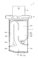
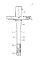
- FIG. 1 to 3 are views showing the external appearance of the physical quantity detection device
- FIG. 1 is a front view of the physical quantity detection device
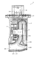
- FIG. 2 is a rear view of the housing
- FIG. 3 is a right side view of the physical quantity detection device. is there.
- the physical quantity detection device 1 of the present embodiment is for detecting the physical quantity of intake air drawn into an internal combustion engine of an automobile, and is attached to the intake pipe of the internal combustion engine.
- the physical quantity detection device 1 is used by being inserted into the intake pipe through a mounting hole provided in the passage wall of the intake pipe.
- the physical quantity detection device 1 includes a housing 2 and a cover 3 attached to the housing 2.
- the housing 2 is configured by injection molding a synthetic resin material
- the cover 3 is configured by a plate-shaped member made of a conductive material such as an aluminum alloy.
- the cover 3 is formed in a thin plate shape and has a wide flat cooling surface.
- the housing 2 has a flange 21 for fixing the physical quantity detection device 1 to the intake pipe, a connector 23 protruding from the flange 21 and exposed to the outside from the intake body for electrical connection with an external device, and the flange 21. It has a measuring unit 22 extending from.
- the measuring unit 22 has a thin and long shape that extends straight from the flange 21, and has a wide front surface 221 and a rear surface 222, and a pair of narrow side surfaces 223 and 224.
- the measurement unit 22 projects from the inner wall of the intake pipe toward the passage center of the intake pipe in a state where the physical quantity detection device 1 is attached to the intake pipe.
- the front surface 221 and the back surface 222 are arranged parallel to each other along the central axis of the intake pipe, and the side surface 223 of the narrow side surfaces 223, 224 of the measurement portion 22 on the one short side of the measurement portion 22 serves as the intake pipe.
- the side surface 224 on the other side in the short-side direction of the measurement unit 22 is disposed so as to face the upstream side and faces the downstream side of the intake pipe. With the physical quantity detection device 1 attached to the intake pipe, the tip of the measurement unit 22 is the lower surface 225.
- the auxiliary passage inlet 201 is provided at the tip of the thin and long measuring portion 22 extending from the flange 21 toward the center of the intake pipe, the measurement error related to the decrease in the flow velocity near the inner wall surface is eliminated. It can be reduced. Further, in the physical quantity detection device 1, not only the auxiliary passage inlet 201 is provided at the tip of the measuring portion 22 extending from the flange 21 toward the center of the intake pipe, but also the first outlet 202 and the second outlet of the auxiliary passage are provided. Since 203 is also provided at the tip of the measurement unit 22, the measurement error can be further reduced.
- the physical quantity detection device 1 has a shape in which the measurement unit 22 extends long along the axis extending from the outer wall of the intake pipe toward the center, but the widths of the side surfaces 223 and 224 are narrow as shown in FIG. Is made. Accordingly, the physical quantity detection device 1 can suppress the fluid resistance to a small value with respect to the gas to be measured.
- the measurement unit 22 of the physical quantity detection device 1 is inserted inside from a mounting hole provided in the intake pipe, the flange 21 of the physical quantity detection device 1 is brought into contact with the intake pipe, and is fixed to the intake pipe with a screw.
- the flange 21 has a substantially rectangular shape in plan view having a predetermined plate thickness.
- the connector 23 has an external terminal 231 provided therein.
- the external terminal 231 is a terminal for outputting a physical quantity such as a flow rate and a temperature, which is a measurement result of the physical quantity detection device 1, and a power supply terminal for supplying DC power for operating the physical quantity detection device 1.
- the housing 2 is provided with a sub-passage groove 210 for forming a sub-passage and a circuit chamber 213 for accommodating the circuit board 4.
- the circuit chamber 213 and the sub-passage groove 210 are recessed in the back surface 222 of the measuring unit 22.
- the circuit chamber 213 is provided in a region on the upstream side in the flow direction of the gas to be measured in the intake pipe on the one side in the lateral direction (side surface 223 side).
- the sub passage groove 210 is located in a region on the distal end side (lower surface 225 side) in the longitudinal direction of the measurement unit 22 with respect to the circuit chamber 213 and a position downstream of the circuit chamber 213 in the flow direction of the measured gas in the intake pipe. It is provided over the region on the other side in the lateral direction (side surface 224 side).
- the sub passage groove 210 forms a sub passage in cooperation with the cover 3.
- the sub passage is provided so as to extend along the protruding direction (longitudinal direction) of the measuring unit 22.
- the sub-passage groove 210 that forms the sub-passage has a first sub-passage groove 211 and a second sub-passage groove 212 that branches in the middle of the first sub-passage groove 211.
- the first sub passage groove 211 is measured between the sub passage inlet 201 opening to the side surface 223 on one side of the measuring unit 22 and the first outlet 202 opening to the side surface 224 on the other side of the measuring unit 22. It is formed so as to extend along the lateral direction of the portion 22.
- the first sub-passage groove 211 constitutes a first sub-passage that takes in the measurement gas flowing in the intake pipe from the sub-passage inlet 201 and returns the taken measurement gas from the first outlet 202 to the intake pipe.
- the first sub passage extends from the sub passage inlet 201 along the flow direction of the gas to be measured in the intake pipe and is connected to the first outlet 202.
- the second sub passage groove 212 is branched at an intermediate position of the first sub passage groove 211, is bent toward the base end side (flange side) of the measurement unit 22, and extends along the longitudinal direction of the measurement unit 22. Exists Then, the base end portion of the measurement unit 22 bends toward the other short-side direction (side surface 224 side) of the measurement unit 22, makes a U-turn toward the tip end of the measurement unit 22, and again in the longitudinal direction of the measurement unit 22. Extend along. Then, it is bent in front of the first outlet 202 toward the other side in the lateral direction of the measuring unit 22, and is provided so as to be continuous with the second outlet 203 opening to the side surface 224 on the other side of the measuring unit 22. ..
- the second outlet 203 is arranged so as to face the downstream side in the flow direction of the measured gas in the intake pipe.
- the second outlet 203 has an opening area that is almost the same as or slightly larger than that of the first outlet 202, and is formed at a position adjacent to the first outlet 202 on the proximal side in the longitudinal direction of the measuring unit 22.
- the second sub-passage groove 212 constitutes a second sub-passage through which the gas to be measured branched from the first sub-passage passes and is returned from the second outlet 203 to the intake pipe.
- the second auxiliary passage has a path that reciprocates along the longitudinal direction of the measuring unit 22. That is, the second sub-passage is branched in the middle of the first sub-passage, extends toward the base end side of the measurement unit 22, is folded back at the base end side of the measurement unit 22, and is then folded back.
- the flow rate detection element 53 is arranged at an intermediate position in the second sub passage groove 212.
- the second sub passage groove 212 can secure a longer passage length of the second sub passage, and can reduce the influence on the flow rate detection element 53 when pulsation occurs in the intake pipe.
- the sub passage can be formed along the extending direction of the measuring unit 22, and the length of the sub passage can be sufficiently long.
- the physical quantity detection device 1 can include a sub passage having a sufficient length. Therefore, the physical quantity detection device 1 can suppress the fluid resistance to a small value and can measure the physical quantity of the gas to be measured with high accuracy.
- the first sub-passage groove 211 extends from the sub-passage inlet 201 to the first outlet 202 along the lateral direction of the measuring unit 22, and therefore enters the sub-passage inlet 201 into the first sub-passage. Foreign matter such as dust can be discharged as it is from the first outlet 202. Therefore, it is possible to prevent foreign matter from entering the second auxiliary passage and prevent the flow rate detecting element 53 in the second auxiliary passage from being affected.
- the sub passage inlet 201 and the first outlet 202 of the first sub passage groove 211 have a larger opening area at the sub passage inlet 201 than at the first outlet 202.
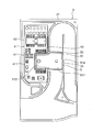
- FIG. 6 is a diagram illustrating the configuration of the cover assembly.
- the cover assembly includes a cover 3 and a circuit board 4 on which the chip package 5 is mounted.
- the cover 3 is made of a metal conductive material such as an aluminum alloy or a stainless alloy.
- the cover 3 is made of a flat plate member having a size that covers the back surface 222 of the measuring unit 22, and is fixed to the measuring unit 22 with an adhesive.
- the cover 3 covers the circuit chamber 213 of the measurement unit 22 and forms a sub-passage in cooperation with the first sub-passage groove 211 and the second sub-passage groove 212 of the measurement unit 22.
- the cover 3 is electrically connected to the ground by interposing a conductive intermediate member between the cover 3 and a predetermined connector terminal, and has a static elimination function.
- the circuit board 4 on which the chip package 5 is mounted is fixed to the back surface of the cover 3.
- the circuit board 4 has a board body 41 made of, for example, a printed board.
- the substrate body 41 has a rectangular shape extending along the longitudinal direction of the measuring unit 22.
- the chip package 5 is fixed to the circuit board 4 at a central position in the longitudinal direction of the circuit board 4 in a state of protruding laterally from the end along the lateral direction of the circuit board 4.
- the package body 51 of the chip package 5 includes a base end portion 512 in which at least a part in the thickness direction is accommodated in the accommodation portion 412 of the circuit board 4, and an end portion of the circuit board 4 along the lateral direction of the circuit board 4. It has a tip portion 511 protruding laterally from.
- the cover assembly accommodates the circuit board 4 in the circuit chamber 213 and extends the chip package 5 between the sub passage and the circuit chamber 213 by attaching the cover 3 to the back surface 222 of the housing 2.
- the tip portion 511 of the package body 51 can be arranged in the sub passage.
- a flow rate detection element 53 is provided at the tip portion 511 of the package body 51, and the detection section of the flow rate detection section is arranged to be exposed in the second sub passage groove 212.
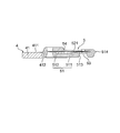
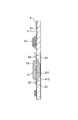
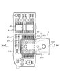
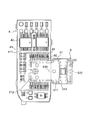
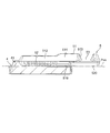
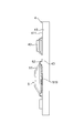
- FIG. 7A is a front view of a circuit board on which a chip package and circuit components are mounted
- FIG. 7B is a cross-sectional view taken along line VIIB-VIIB of FIG. 7A
- FIG. 7C is a cross-sectional view taken along line VIIC-VIIC of FIG. 7A.
- the circuit board 4 is provided with an accommodating portion 412 for accommodating a part of the chip package 5.
- the accommodating portion 412 is configured by partially cutting out a portion that is deviated to the one side in the lateral direction at the center of the substrate body 41 in the longitudinal direction (notch portion).
- Reference numeral 41 has a substantially U shape in a plan view.
- the package body 51 in the thickness direction of the chip package 5 is accommodated in the accommodation portion 412 of the circuit board 4.
- the package front surface of the package body 51 which is the base end portion 512 and the surface of the package body 51 on which the flow rate detection element 53 is provided, is accommodated in the accommodation portion 412 of the circuit board 4. ..
- a part of the package body 51 in the thickness direction is housed in the housing portion 412 of the circuit board 4, so that the overall mounting height including the thickness of the chip package 5 and the height of the terminals is suppressed. be able to.
- the mounting height can be reduced to the same as that of a small pressure sensor mounted on the circuit board 4 together with the chip package 5.
- the mounting height of the mounted components can be suppressed to be lower than that in the case where the chip package 5 is mounted on the circuit board 4 in an overlapping manner. Therefore, the height of the measurement unit 22 can be reduced, the physical quantity detection device 1 can be made thin, and the flow resistance in the main passage in the intake pipe can be reduced.
- the case where a part of the package body 51 in the thickness direction is housed in the housing portion 412 of the circuit board 4 has been described as an example, but the entire package body 51 in the thickness direction is housed. It may be configured to be. With such a configuration, the height of the measuring unit 22 can be further promoted, and the physical quantity detection device 1 can be thinned.
- the chip package 5 is provided with a plurality of connecting terminals 52 protruding from the base end portion 512 of the package body 51. By connecting these connecting terminals 52 to the pads 43 of the circuit board 4 by soldering, the circuit board 4 is formed. Is integrally fixed to.
- the chip package 5 is mounted with a flow rate detection element 53 and an LSI that is an electronic component that drives the flow rate detection element 53.
- the base end portion 512 of the chip package 5 is provided with a plurality of connection terminals 52 that protrude in the direction away from each other along the lateral direction of the package body 51.
- a plurality of pads 43 are separately provided on one side and the other side in the longitudinal direction of the circuit board 4, which are locations facing each other with the accommodating portion 412 interposed therebetween.
- the plurality of connection terminals 52 of the chip package 5 are soldered to the respective pads 43.
- the plurality of connection terminals 52 form a solder fixing portion that solder-fixes the chip package 5 to the circuit board 4.
- the chip package 5 is configured by mounting the LSI 54 and the flow rate detecting element 53 on the lead frame 521 and sealing with a thermosetting resin.
- the chip package 5 has a package body 51 that is resin-molded into a substantially flat plate shape.
- the package main body 51 has a rectangular shape, extends along the lateral direction of the measurement unit 22, and the base end 512 on one longitudinal side of the package main body 51 is accommodated in the accommodation chamber 412 of the circuit board 4.
- the tip portion 511 on the other longitudinal side of the package body 51 is arranged so as to project from the circuit board 4.
- the flow rate detecting element 53 of the chip package 5 is provided so that the detecting portion is exposed in the passage groove 513 formed in the surface of the package body 51.
- the passage groove 513 extends from the one end in the lateral direction to the end in the other lateral direction of the package body 51 so as to extend along the second auxiliary passage groove 212 in the second auxiliary passage groove 212. Is formed over the entire width of.
- the flow rate detection element 53 has a diaphragm structure.
- connection terminals 52 of the chip package 5 are provided so as to project in the lateral direction of the package body 51 from the center of the package body 51 in the thickness direction.
- the connection terminal 52 has a facing surface facing the pad 43 of the circuit board 4, and the position of the facing surface is set to the same height as the mounting surface of the lead frame 521.
- the chip package 5 is electrically connected by soldering the plurality of connection terminals 52 provided on the base end portion 512 of the package body 51 to the plurality of pads 43 of the circuit board 4, and is integrated with the circuit board 4. Fixed.
- the base end portion 512 of the chip package 5 is fixed to the circuit board 4, the tip end portion 511 projects from the circuit board 4, and the chip package 5 is so-called cantilevered with respect to the circuit board 4.
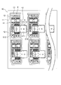
- FIG. 8A is a front view of the substrate sheet
- FIG. 8B is a bottom view of the substrate sheet.
- the chip package 5 is mounted on the circuit board 4 by solder reflow. As shown in FIGS. 8A and 8B, the chip package 5 is conveyed to a reflow furnace in a state of being set on the substrate sheet 10, and solder reflow is executed in the reflow furnace.
- the board sheet 10 has a plurality of circuit boards 4 arranged side by side in a plane and a waste board 11 that supports the plurality of circuit boards 4.
- the discard board 11 has a gap 13 between each of the circuit boards 4 and supports each of the circuit boards 4 via the gate 12.
- the discard board 11 is provided with a notch 14 corresponding to each circuit board 4, and when the chip package 5 is set on the board sheet 10, the tip end 511 of the chip package 5 is accommodated. ing.
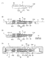
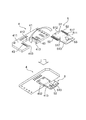
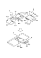
- FIG. 9 is a process diagram of assembling the chip package.
- the chip package 5 is placed on the substrate sheet 10 and set at a predetermined position in a posture in which the package front surface portion and the package rear surface portion of the chip package 5 are located on the lower side and the upper side, respectively.
- the base end portion 512 is accommodated in the accommodation portion 412 of the circuit board 4, and the tip end portion 511 is accommodated in the cutout portion 14 of the waste substrate 11.
- connection terminals 52 of the chip package 5 are placed on the pads 43 provided on the mounting surface 411 of the circuit board 4, and the base end portion 512 of the package body 51 is supported by the circuit board 4. Since the chip package 5 is arranged so that the tip portion 511 of the package body 51 projects from the circuit board 4, the center of gravity is located closer to the tip portion 511 side than the base end portion 512. Therefore, if the connection terminals 52 of the package body 51 are simply placed and supported on the pads 43 of the circuit board 4, the balance is unbalanced, and the chip package 5 may be inclined such that the tip portion 511 of the package body 271 is lowered.
- the positioning portion for positioning the chip package 5 with respect to the circuit board 4.
- the positioning portion is provided at a position closer to the flow rate detecting element 53 than the connection terminal 52 of the chip package 5.
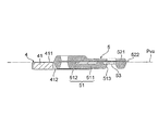
- the positioning portion has a convex portion 514 formed so as to project in the center of the edge of the tip portion 511 of the package body 51.
- the convex portion 514 is made of a molding resin and is integrally formed when the package body 51 is molded.
- the convex portion 514 has a mounting surface that is placed on the discarding substrate 11.
- the mounting surface of the convex portion 514 has the same height as the facing surface of the connection terminal 52, and when the chip package 5 is mounted on the circuit board 4, the mounting surface is on the virtual plane Pva including the mounting surface 411 of the circuit board 4. It is supposed to be located.
- the convex portion 514 is placed on the discarding substrate 11 to support the tip portion 511 of the package body 51 on the circuit board 4.
- the base end portion 512 of the package body 51 is supported by the circuit board 4 and the tip end portion 511 is supported by the discard board 11. Therefore, it is possible to prevent the chip package 5 from tilting so that the tip portion 511 of the package body 51 is lowered with respect to the substrate sheet 10.
- the chip package 5 is conveyed to the reflow furnace in a state of being set on the board sheet 10, solder reflow is executed in the reflow furnace, and is fixed to the circuit board 4 by soldering.
- the gate 12 is cut, and the circuit board 4 is separated from the discarded board 11 as shown in FIG. 9C. Then, it is attached to the cover 3 to form a cover assembly, and is attached to the housing 2 as shown in FIG. 9 (4).
- the adhesive 6 is applied between the protrusion 32 and the protrusion 514 of the cover 3.
- the tip portion 511 of the package body 51 can be fixed to the cover 3, and the chip package 5 can be stably supported by the cover 3. Therefore, it is possible to prevent the ratio of the cross-sectional area D1 on the flow rate detecting element 53 side of the sub-passage and the cross-sectional area D2 on the package back surface side of the sub-passage from changing due to displacement or vibration of the chip package 5, and to obtain good mounting accuracy. it can.
- the convex portion 514 is provided at the center of the edge of the tip portion 511 of the package body 51 so that when the chip package 5 is set on the substrate sheet 10, it can be placed on the discarded substrate 11. It has become. Therefore, the chip package 5 can be reliably positioned with respect to the circuit board 4 and stably supported in a preset posture state. Therefore, the position and orientation of the chip package 5 can be prevented from changing during the solder reflow, and the chip package 5 can be fixed to the circuit board 4 by soldering at a preset position and orientation. Variation can be reduced. Therefore, the inclination of the chip package 5 which is cantilevered on the circuit board 4 can be controlled, and good mounting accuracy at the time of solder reflow and mounting accuracy including variations in solder thickness can be easily secured.
- the flow rate characteristic of the physical quantity detection device 1 depends on the relationship between the cross-sectional area D1 on the package front surface side of the sub-passage and the cross-sectional area D2 on the package back surface side.
- the convex portion 514 is provided at a place where the flatness of the mounting surface 411 of the circuit board 4 and the flow rate detecting element 53 is established, that is, on the flow rate detecting element 53 side rather than the connection terminal 52 side.
- the mounting surface to be mounted on the waste substrate 11 is at the same height as the facing surface of the connection terminal 52, and when the chip package 5 is mounted on the circuit board 4, It is arranged on a virtual plane Pva including four mounting surfaces 411.
- the chip package 5 can be easily arranged in parallel to the circuit board 4. Therefore, in the physical quantity detection device 1, the sub-passage cross-sectional area on the side where the flow rate detection element 53 is exposed can be made constant, and the flow rate detection accuracy can be stabilized.
- FIG. 10A is a front view of a circuit board according to the second embodiment
- FIG. 10B is a sectional view taken along line XB-XB of FIG. 10A.
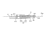
- the positioning portion is configured by the convex portion 522 that extends a part of the lead frame 521 and projects from the package body 51 of the chip package 5.
- the chip package 5 has a lead frame 521 inside the package body 51.
- the lead frame 521 is provided between the base end portion 512 and the tip end portion 511 of the package main body 51, the connection terminal 52 projects from the base end portion 512, and the convex portion serving as a positioning portion from the tip end portion 511. 522 is protruding.
- the convex portion 522 is configured by a tie bar of the lead frame 521 protruding from the edge of the tip portion 511 of the package body 51.
- the convex portion 522 is placed on the discarding substrate 11 when the chip package 5 is set on the substrate sheet 10, and the tip portion 511 of the package body 51. Can be supported on the substrate sheet 10. Therefore, similarly to the first embodiment, the chip package 5 can be reliably positioned with respect to the circuit board 4 and stably supported in the preset posture state. Therefore, the position and orientation of the chip package 5 can be prevented from changing during the solder reflow, and the chip package 5 can be fixed to the circuit board 4 by soldering at a preset position and orientation. Variation can be reduced.
- the mounting surface of the convex portion 522 has the same height as the facing surface of the connection terminal 52, and when the chip package 5 is mounted on the circuit board 4, the mounting surface is on the virtual plane Pva including the mounting surface 411 of the circuit board 4. It is supposed to be located. Therefore, by simply mounting the chip package 5 on the board sheet 10, the chip package 5 can be easily arranged in parallel to the circuit board 4. Therefore, the sectional area of the sub-passage on the side where the flow rate detecting element 53 is exposed can be made constant, and the detection accuracy can be stabilized.
- the convex portion 522 is provided by projecting a part of the lead frame 521 from the package body 51 of the chip package 5, the positioning portion can be easily provided on the chip package 5, which is easy. Can be carried out.
- FIG. 11A is a front view of a circuit board according to a third embodiment
- FIG. 11B is a sectional view taken along line XIB-XIB of FIG. 11A.
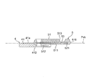
- the positioning portion is composed of the convex portion 523 formed by projecting a part of the lead frame 521.
- the tip of the convex portion 523 is bent so that when the chip package 5 is set on the substrate sheet 10, the convex portion 523 is inserted into the insertion hole 15 provided in advance in the discarded substrate 11.
- the convex portion 523 is formed in an L shape projecting from the package body 51 of the chip package 5, bent at the tip, and the opposing surface of the connection terminal 52 projecting to the opposite side.
- the discard board 11 is provided with an insertion hole 15 into which the tip of the convex portion 523 is inserted when the chip package 5 is set on the board sheet 10.
- the chip package 5 when the chip package 5 is set on the substrate sheet 10, the protrusion 523 is placed on the discarding substrate 11 and the tip of the protrusion 523 is inserted into the insertion hole 15. Therefore, the chip package 5 is arranged in parallel with the mounting surface 411 of the circuit board 4, and movement of the chip package 5 in the direction along the mounting surface 411 of the circuit board 4 is restricted. Therefore, the chip package 5 can be reliably positioned with respect to the circuit board 4 and stably supported in a preset posture state. Therefore, the position and orientation of the chip package 5 can be prevented from changing during the solder reflow, and the chip package 5 can be fixed to the circuit board 4 by soldering at a preset position and orientation. Variation can be reduced. Therefore, the inclination of the chip package 5 which is cantilevered on the circuit board 4 can be controlled, and good mounting accuracy at the time of solder reflow and mounting accuracy including variations in solder thickness can be easily ensured.
- FIG. 12A is a front view of a circuit board according to a fourth embodiment
- FIG. 12B is a sectional view taken along line XIIB-XIIB of FIG. 12A.
- a convex portion 515 extending along the edge of the tip portion 511 of the package body 51 is provided.
- the convex portion 515 is made of a molding resin, and is integrally formed when the package body 51 is molded.
- the convex portion 515 is formed by projecting the package back surface side more than the package front surface side and providing a step between the package front surface portion and the package back surface portion.
- the convex portion 515 has a mounting surface of the convex portion 515 at the same height as the facing surface of the connection terminal 52, and when the chip package 5 is mounted on the circuit board 4, it includes a mounting surface 411 of the circuit board 4. It is located on the plane Pva.
- the convex portion 515 is placed on the discarding substrate 11 during solder reflow, and the chip package 5 can be positioned with respect to the circuit board 207. Therefore, by simply mounting the chip package 5 on the board sheet 10, the chip package 5 can be easily arranged in parallel to the circuit board 4. Therefore, in the physical quantity detection device 1, the sub-passage cross-sectional area on the side where the flow rate detection element 53 is exposed can be made constant, and the flow rate detection accuracy can be stabilized.
- the adhesive 6 is applied between the protrusions 32 of the cover 3 and fixed to the cover 3. Since the adhesive 6 is applied along the edge of the tip portion 511 of the package body 51, it can be bonded over a longer distance than the convex portion 514 in the first embodiment. Therefore, the tip portion 511 of the package body 51 can be securely fixed to the protrusion 32 of the cover 3, and the sub passage can be sealed so as to be completely divided into the package front surface side and the package back surface side.
- the package main body 51 since the package back surface side is projected more than the package front surface side and the step is provided between the package front surface portion and the package back surface portion, the package main body 51 The position of the edge of the front end portion 511 on the package front surface side can be arranged closer to the flow rate detecting element 53 side than the position of the edge on the package back surface side, and even when the width of the second sub passage is narrow. It is possible to secure the passage groove 513 sufficiently wide.
- FIG. 13A is a front view of the circuit board in the fifth embodiment
- FIG. 13B is a sectional view taken along line XIIIB-XIIIB of FIG. 13A
- FIG. 13C is a sectional view taken along line XIIIC-XIIIC of FIG. 13A.
- the orientation of the chip package 5 with respect to the circuit board 4 is opposite to that of each of the above-described embodiments.
- the chip package 5 is arranged such that the exposed surface of the flow rate detection element 53 and the facing surface of the connection terminal 52 are separated from each other.
- the convex portion 516 is provided at the center of the edge of the tip portion 511 of the package body 51.
- the convex portion 516 is made of a molding resin, and is integrally formed when the package body 51 is molded.
- the convex portion 516 has a mounting surface that is mounted on the discarding substrate 11 when the chip package 5 is set on the substrate sheet 10.
- the mounting surface of the convex portion 516 has the same height as the facing surface of the connection terminal 52, and when the chip package 5 is mounted on the circuit board 4, the mounting surface is on the virtual plane Pvb including the mounting surface 411 of the circuit board 4. It is supposed to be located. Therefore, by simply mounting the chip package 5 on the board sheet 10, the chip package 5 can be easily arranged in parallel to the circuit board 4. Therefore, in the physical quantity detection device 1, the sub-passage cross-sectional area on the side where the flow rate detection element 53 is exposed can be made constant, and the flow rate detection accuracy can be stabilized.
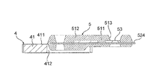
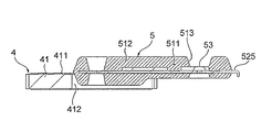
- FIGS. 14A and 14B are cross-sectional views showing modified examples of the circuit board shown in FIG. 13B.
- the configuration shown in FIGS. 10A and 10B in the second embodiment is applied, and the package body 51 of the chip package 5 to a part of the lead frame 521 is applied. Is provided with a protruding portion 524.
- the configuration described with reference to FIGS. 11A and 11B in the third embodiment is applied, and the protrusion 525 having a bent tip is provided. Is.
- the convex portion 525 whose tip is bent is designed such that when the chip package 5 is set on the substrate sheet 10, the tip is inserted into the insertion hole 15 that is provided in the waste substrate 11 in advance.
- the modified examples shown in FIGS. 14A and 14B can obtain the same effects as those of the second and third embodiments.
- ⁇ Sixth Embodiment> 15A and 15B are perspective views illustrating a sixth embodiment.
- the positioning portion of this embodiment is fitted to the package recess 517 or the package protrusion 518 formed on the chip package 5 and the board protrusion 413 or the package protrusion 518 formed on the circuit board 4 and fitted into the package recess 517.
- a substrate recess 414 that fits.
- the package recess 517 is recessed in the package surface of the package body 51.
- the package recessed portion 517 is provided in a pair between the base end portion 512 and the tip end portion 511 of the package body 51 and at positions separated from one side and the other side in the lateral direction of the package body 51.
- the board convex portion 413 is formed so as to project toward the mutually approaching direction at the entrance portion of the housing portion 412 of the board body 41, and by mounting the chip package 5 on the circuit board 4, the package concave portion 517 is formed. It is designed to be pressed into.
- the chip package 5 is positioned and fixed to the circuit board 4 by press-fitting the board protrusion 413 into the package recess 517, and the connection terminals 52 of the chip package 5 are in contact with the pads 43 of the circuit board 4. To be done. Therefore, the connection terminals 52 of the chip package 5 can be soldered to the pads 43 of the circuit board 4, and the chip package 5 can be fixed to the circuit board 4 by soldering, by transporting the connection terminal 52 of the chip package 5 to the circuit board 4 in that state.
- the package protrusion 518 is provided on the package surface of the package body 51.
- the package protrusions 518 are provided as a pair at a position between the base end portion 512 and the tip end portion 511 of the package body 51 and apart from one side and the other side in the lateral direction of the package body 51. ..
- the board concave portion 414 is formed in a concave shape in a direction away from each other at the entrance portion of the housing portion 412 of the board body 41. It is supposed to be done.
- the chip package 5 is positioned and fixed to the circuit board 4 by pressing the package convex portion 518 into the board concave portion 414, and the connection terminals 52 of the chip package 5 are in contact with the pads 43 of the circuit substrate 4. To be done. Therefore, the connection terminals 52 of the chip package 5 can be soldered to the pads 43 of the circuit board 4, and the chip package 5 can be fixed to the circuit board 4 by soldering, by transporting the connection terminal 52 of the chip package 5 to the circuit board 4 in that state.
- the chip package 5 is provided with the package recess 517 or the package protrusion 518
- the circuit board 4 is provided with the substrate protrusion 413 or the substrate recess 414.
- the chip package 5 can be reliably positioned with respect to the circuit board 4 and stably supported in a preset posture state. Therefore, the position and orientation of the chip package 5 can be prevented from changing during the solder reflow, and the chip package 5 can be fixed to the circuit board 4 by soldering at a preset position and orientation. Variation can be reduced. Therefore, the inclination of the chip package 5 which is cantilevered on the circuit board 4 can be controlled, and good mounting accuracy at the time of solder reflow and mounting accuracy including variations in solder thickness can be easily secured. Further, according to the present embodiment, the chip package 5 can be positioned only by assembling the chip package 5 on the circuit board 4, so that the waste substrate 11 of each of the above-described embodiments can be omitted.
- FIG. 16A is a front view of the circuit board in the seventh embodiment
- FIG. 16B is a bottom view of the circuit board shown in FIG. 16A
- FIG. 16C is a right side view of the circuit board shown in FIG. 16A.
- a characteristic of this embodiment is that the chip package 5 is arranged on the mounting surface 411 of the substrate body 41.
- the circuit board 4 has a substantially rectangular shape in which the housing portion 412 is omitted in the board body 41.
- the chip package 5 is arranged on the mounting surface 411 of the circuit board 4 in a posture in which the package back surface of the chip package 5 faces the mounting surface 411 of the circuit board 4.
- the connecting terminal 52 of the chip package 5 has an opposing surface arranged at a position projecting in the thickness direction of the package body 51 from the back surface of the package.
- a positioning portion for positioning and fixing the chip package 5 is provided on the back surface of the package of the chip package 5.
- the positioning portion is provided at a position closer to the tip end portion 511 than the base end portion 512 of the chip package 5, and has convex portions 519 and 520.
- the protrusions 519 and 520 are made of a molding resin and are integrally formed when the package body 51 is molded.
- the convex portions 519 and 520 are provided one by one at the center position in the lateral direction of the package body 51.
- the convex portion 519 is arranged at a position facing the mounting surface 411 of the circuit board 4, and the convex portion 520 is arranged at a position facing the discarding substrate 11 (see FIG. 8).
- the convex portions 519 and 520 have the same height as the facing surface of the connection terminal 52, and are located on the virtual plane Pva including the mounting surface 411 of the circuit board 5 when the chip package 5 is placed on the circuit board 4. It is like this.
- the chip package 5 can be easily arranged in parallel to the circuit board 4. Therefore, in the physical quantity detection device 1, the sub-passage cross-sectional area on the side where the flow rate detection element 53 is exposed can be made constant, and the flow rate detection accuracy can be stabilized.
- the projecting portions 519 and 520 are provided on the package back surface of the tip portion 511 of the package body 51, and when the chip package 5 is set on the substrate sheet 10, the circuit board 4 and the waste substrate 11 are provided. It is supposed to be supported on. Therefore, the chip package 5 can be reliably positioned with respect to the circuit board 4 and stably supported in a preset posture state. Therefore, the position and orientation of the chip package 5 can be prevented from changing during the solder reflow, and the chip package 5 can be fixed to the circuit board 4 by soldering at a preset position and orientation. Variation can be reduced. Therefore, it is possible to control the inclination of the chip package 5 which is cantilevered on the circuit board 4 and easily secure good mounting accuracy during solder reflow and mounting accuracy including variations in solder thickness.
Landscapes
- Engineering & Computer Science (AREA)
- Microelectronics & Electronic Packaging (AREA)
- Manufacturing & Machinery (AREA)
- Physics & Mathematics (AREA)
- Fluid Mechanics (AREA)
- General Physics & Mathematics (AREA)
- Measuring Volume Flow (AREA)
- Structures Or Materials For Encapsulating Or Coating Semiconductor Devices Or Solid State Devices (AREA)
- Structures For Mounting Electric Components On Printed Circuit Boards (AREA)
- Measuring Fluid Pressure (AREA)
Abstract
Description
図1から図3は、物理量検出装置の外観を示す図であり、図1は、物理量検出装置の正面図、図2は、ハウジングの背面図、図3は、物理量検出装置の右側面図である。
本実施例の物理量検出装置1は、自動車の内燃機関に吸入される吸入空気の物理量を検出するためのものであり、内燃機関の吸気管に装着される。
カバー組立体は、カバー3と、チップパッケージ5を実装する回路基板4によって構成されている。カバー3は、例えばアルミニウム合金やステンレス合金などの金属製の導電性材料によって構成されている。カバー3は、計測部22の背面222を覆う大きさを有する平板部材からなり、接着剤によって計測部22に固定される。カバー3は、計測部22の回路室213を覆い、また、計測部22の第1副通路溝211および第2副通路溝212との協働により副通路を構成する。カバー3は、所定のコネクタターミナルとの間に導電性の中間部材を介在させることによってグランドに電気的に接続されており、除電機能を有している。
具体的には、パッケージ本体51の基端部512でかつパッケージ本体51の流量検出素子53が設けられる面側であるパッケージ表面部が回路基板4の収容部412に入り込んだ状態で収容されている。
複数の接続端子52は、チップパッケージ5を回路基板4にはんだ固定するはんだ固定部を構成する。
チップパッケージ5は、はんだリフローによって回路基板4に実装される。チップパッケージ5は、図8A及び図8Bに示すように、基板シート10にセットされた状態でリフロー炉に搬送され、リフロー炉内ではんだリフローが実行される。
チップパッケージ5は、チップパッケージ5のパッケージ表面部とパッケージ裏面部とが下側と上側に位置する姿勢状態で、基板シート10の上から載せられて、所定位置にセットされる。チップパッケージ5は、基板シート10にセットされることにより、基端部512が回路基板4の収容部412に収容され、かつ、先端部511が捨て基板11の切り欠き部14に収容される。
図10Aは、第2の実施例における回路基板の正面図、図10Bは、図10AのXB-XB線断面図である。
図11Aは、第3の実施例における回路基板の正面図、図11Bは、図11AのXIB-XIB線断面図である。
図12Aは、第4の実施例における回路基板の正面図、図12Bは、図12AのXIIB-XIIB線断面図である。
図13Aは、第5の実施例における回路基板の正面図、図13Bは、図13AのXIIIB-XIIIB線断面図、図13Cは、図13AのXIIIC-XIIIC線断面図である。
図14Aに示す変形例は、凸部516の代わりに、第2の実施例において図10A及び図10Bに示して説明した構成を適用し、チップパッケージ5のパッケージ本体51からリードフレーム521の一部を突出させた凸部524を設けたものである。そして、図14Bに示す変形例は、凸部516の代わりに、第3の実施例において図11A及び図11Bに示して説明した構成を適用し、先端が折り曲げられた凸部525を設けたものである。先端が折り曲げられた凸部525は、チップパッケージ5を基板シート10にセットした際に、捨て基板11に予め設けられている挿入穴15に先端が挿入されるようになっている。図14A及び図14Bに示す各変形例は、第2の実施例及び第3の実施例と同様の作用効果を得ることができる。
図15A及び図15Bは、第6の実施例を説明する斜視図である。
本実施例の位置決め部は、チップパッケージ5に形成されたパッケージ凹部517又はパッケージ凸部518と、回路基板4に形成されてパッケージ凹部517に嵌合する基板凸部413又はパッケージ凸部518に嵌合する基板凹部414と、を有する。
また、本実施例によれば、回路基板4にチップパッケージ5を組み付けるだけでチップパッケージ5を位置決めできるので、上述の各実施例の捨て基板11を省略することもできる。
図16Aは、第7の実施例における回路基板の正面図、図16Bは、図16Aに示す回路基板の下面図、図16Cは、図16Aに示す回路基板の右側面図である。
4 回路基板
5 チップパッケージ
43 パッド
51 パッケージ本体
52 接続端子(はんだ固定部)
53 流量検出素子
413 基板凸部
414 基板凹部
514、515、516、522、523、524、525 凸部(位置決め部)
517 パッケージ凹部(位置決め部)
518 パッケージ凸部(位置決め部)
Claims (9)
- 検出部が少なくとも露出するように流量検出素子を樹脂で封止したチップパッケージを回路基板に位置決め固定する位置決め固定構造であって、
前記チップパッケージは、前記回路基板にはんだ固定されるはんだ固定部と、前記回路基板に対する位置決めを行うための位置決め部とを備え、
前記位置決め部は、前記はんだ固定部よりも前記流量検出素子側に設けられることを特徴とするチップパッケージの位置決め固定構造。 - 前記位置決め部は、
前記チップパッケージに形成されたパッケージ凹部又はパッケージ凸部と、
前記回路基板に形成されて前記パッケージ凹部に嵌合する基板凸部又は前記パッケージ凸部に嵌合する基板凹部と、を有することを特徴とする請求項1に記載のチップパッケージの位置決め固定構造。 - 前記チップパッケージは、前記はんだ固定部が設けられる基端部と、前記位置決め部が設けられる先端部とを有するパッケージ本体を有し、
前記位置決め部は、前記パッケージ本体の先端部に形成された凸部を有し、
前記はんだ固定部は、前記パッケージ本体の基端部から突出する接続端子を有し、
前記凸部と前記接続端子は、前記回路基板の実装面を含む仮想平面上に位置することを特徴とする請求項1に記載のチップパッケージの位置決め固定構造。 - 前記凸部は、前記回路基板を支持する捨て基板に当接されることを特徴とする請求項3に記載のチップパッケージの位置決め固定構造。
- 前記凸部は、前記樹脂により構成されていることを特徴とする請求項3に記載のチップパッケージの位置決め固定構造。
- 前記チップパッケージは、前記流量検出素子を搭載するリードフレームを有し、
前記凸部は、前記リードフレームの一部を前記パッケージ本体から突出させることにより構成されていることを特徴とする請求項4に記載のチップパッケージの位置決め固定構造。 - 前記凸部は、前記リードフレームのフレーム面に沿って前記パッケージ本体から突出し、先端で折曲されて前記接続端子の接続面側に突出するL字形状を有し、
前記捨て基板には、前記凸部の先端が挿入される挿入穴が設けられていることを特徴とする請求項6に記載のチップパッケージの位置決め固定構造。 - 前記凸部は、物理量検出装置のハウジングに前記回路基板を取り付けた場合に、前記ハウジングに接着されることを特徴とする請求項3に記載のチップパッケージの位置決め固定構造。
- 回路基板と該回路基板を切り離し可能に支持する捨て基板とを有する基板シートに、流量検出部を有するチップパッケージを配置する配置工程と、
前記チップパッケージが配置された基板シートをリフロー炉に搬送してはんだリフローを行う工程と、
前記基板シートから前記回路基板を切り離す工程と、を含み、
前記配置工程では、前記基板シートに対して前記流量検出部が前記回路基板から突出するように前記チップパッケージを配置して、前記チップパッケージの基端部に設けられているはんだ固定部を前記回路基板に当接させ、かつ、前記チップパッケージの先端部に設けられている位置決め部を前記捨て基板に当接させて、前記チップパッケージを支持することを特徴とする物理量検出装置の製造方法。
Priority Applications (4)
| Application Number | Priority Date | Filing Date | Title |
|---|---|---|---|
| US17/288,618 US12119287B2 (en) | 2018-11-05 | 2019-09-20 | Chip package positioning and fixing structure |
| DE112019004779.5T DE112019004779B4 (de) | 2018-11-05 | 2019-09-20 | Positionierungs- und befestigungsaufbau für ein chipmodul |
| JP2020556659A JP7026259B2 (ja) | 2018-11-05 | 2019-09-20 | チップパッケージの位置決め固定構造 |
| CN201980065531.XA CN112912699B (zh) | 2018-11-05 | 2019-09-20 | 芯片封装件的定位固定结构 |
Applications Claiming Priority (2)
| Application Number | Priority Date | Filing Date | Title |
|---|---|---|---|
| JP2018208459 | 2018-11-05 | ||
| JP2018-208459 | 2018-11-05 |
Publications (1)
| Publication Number | Publication Date |
|---|---|
| WO2020095548A1 true WO2020095548A1 (ja) | 2020-05-14 |
Family
ID=70612429
Family Applications (1)
| Application Number | Title | Priority Date | Filing Date |
|---|---|---|---|
| PCT/JP2019/036909 Ceased WO2020095548A1 (ja) | 2018-11-05 | 2019-09-20 | チップパッケージの位置決め固定構造 |
Country Status (5)
| Country | Link |
|---|---|
| US (1) | US12119287B2 (ja) |
| JP (1) | JP7026259B2 (ja) |
| CN (1) | CN112912699B (ja) |
| DE (1) | DE112019004779B4 (ja) |
| WO (1) | WO2020095548A1 (ja) |
Families Citing this family (2)
| Publication number | Priority date | Publication date | Assignee | Title |
|---|---|---|---|---|
| JP7162961B2 (ja) | 2019-03-04 | 2022-10-31 | 日立Astemo株式会社 | 流量測定装置 |
| CN116013803B (zh) * | 2023-03-30 | 2023-06-20 | 深圳新控半导体技术有限公司 | 一种芯片粘贴用温感式检测装置及其检测方法 |
Citations (5)
| Publication number | Priority date | Publication date | Assignee | Title |
|---|---|---|---|---|
| JPH05326911A (ja) * | 1992-05-18 | 1993-12-10 | Sony Corp | リニアセンサ |
| JP2011122984A (ja) * | 2009-12-11 | 2011-06-23 | Hitachi Automotive Systems Ltd | 流量センサとその製造方法、及び流量センサモジュール |
| JP2012242298A (ja) * | 2011-05-20 | 2012-12-10 | Denso Corp | 流量検出装置 |
| JP2015017857A (ja) * | 2013-07-10 | 2015-01-29 | 株式会社デンソー | 流量センサ |
| US20160276566A1 (en) * | 2013-10-31 | 2016-09-22 | Robert Bosch Gmbh | Electrical Circuit and Method for Producing an Electrical Circuit |
Family Cites Families (8)
| Publication number | Priority date | Publication date | Assignee | Title |
|---|---|---|---|---|
| AU2003902836A0 (en) * | 2003-06-06 | 2003-06-26 | M.B.T.L. Limited | Environmental sensor |
| JP2005045110A (ja) | 2003-07-24 | 2005-02-17 | Kubota Corp | リフロー半田付け行程における電子部品の位置決め構造 |
| JP2005172526A (ja) * | 2003-12-09 | 2005-06-30 | Denso Corp | 流量測定装置およびその製造方法 |
| JP4882732B2 (ja) * | 2006-12-22 | 2012-02-22 | 株式会社デンソー | 半導体装置 |
| WO2012049742A1 (ja) | 2010-10-13 | 2012-04-19 | 日立オートモティブシステムズ株式会社 | 流量センサおよびその製造方法並びに流量センサモジュールおよびその製造方法 |
| JP5662382B2 (ja) * | 2012-06-15 | 2015-01-28 | 日立オートモティブシステムズ株式会社 | 熱式流量計 |
| CN107003164B (zh) * | 2014-12-08 | 2019-12-03 | 日立汽车系统株式会社 | 物理量检测装置 |
| US11268920B2 (en) * | 2017-09-29 | 2022-03-08 | Hitachi Automotive Systems, Ltd. | Physical quantity detection device |
-
2019
- 2019-09-20 JP JP2020556659A patent/JP7026259B2/ja active Active
- 2019-09-20 WO PCT/JP2019/036909 patent/WO2020095548A1/ja not_active Ceased
- 2019-09-20 DE DE112019004779.5T patent/DE112019004779B4/de active Active
- 2019-09-20 US US17/288,618 patent/US12119287B2/en active Active
- 2019-09-20 CN CN201980065531.XA patent/CN112912699B/zh active Active
Patent Citations (5)
| Publication number | Priority date | Publication date | Assignee | Title |
|---|---|---|---|---|
| JPH05326911A (ja) * | 1992-05-18 | 1993-12-10 | Sony Corp | リニアセンサ |
| JP2011122984A (ja) * | 2009-12-11 | 2011-06-23 | Hitachi Automotive Systems Ltd | 流量センサとその製造方法、及び流量センサモジュール |
| JP2012242298A (ja) * | 2011-05-20 | 2012-12-10 | Denso Corp | 流量検出装置 |
| JP2015017857A (ja) * | 2013-07-10 | 2015-01-29 | 株式会社デンソー | 流量センサ |
| US20160276566A1 (en) * | 2013-10-31 | 2016-09-22 | Robert Bosch Gmbh | Electrical Circuit and Method for Producing an Electrical Circuit |
Also Published As
| Publication number | Publication date |
|---|---|
| CN112912699B (zh) | 2024-03-19 |
| DE112019004779B4 (de) | 2025-10-09 |
| CN112912699A (zh) | 2021-06-04 |
| JP7026259B2 (ja) | 2022-02-25 |
| DE112019004779T5 (de) | 2021-09-09 |
| US20210398886A1 (en) | 2021-12-23 |
| JPWO2020095548A1 (ja) | 2021-10-21 |
| US12119287B2 (en) | 2024-10-15 |
Similar Documents
| Publication | Publication Date | Title |
|---|---|---|
| US11143535B2 (en) | Thermal-type flowmeter | |
| JP6771111B2 (ja) | 物理量検出装置 | |
| KR20000022326A (ko) | 프린트 회로 기판의 장착 표면에 장착된 압력 센서 소자 | |
| JP7026259B2 (ja) | チップパッケージの位置決め固定構造 | |
| US11353350B2 (en) | Physical quantity detection device | |
| JP6915160B2 (ja) | 物理量検出装置 | |
| JP5971221B2 (ja) | 空気流量測定装置 | |
| EP1363110B1 (en) | Device for detecting physical quantity | |
| CN107076593A (zh) | 热式空气流量计 | |
| KR20130126471A (ko) | 플로우 센서 | |
| JP4196546B2 (ja) | 空気流量測定装置 | |
| US11268920B2 (en) | Physical quantity detection device | |
| WO2021166419A1 (ja) | 熱式流量計 | |
| WO2020179249A1 (ja) | 流量測定装置 | |
| JP7062135B2 (ja) | 物理量検出装置 | |
| JP2020094933A (ja) | 熱式流量計 | |
| US20220390264A1 (en) | Flow Rate Measurement Device | |
| JP7225062B2 (ja) | センサ装置 | |
| JP4365982B2 (ja) | 傾斜センサ | |
| CN112136024A (zh) | 物理量检测装置 | |
| CN117242321A (zh) | 物理量检测装置 | |
| JP2019207173A (ja) | 回路パッケージおよび流量測定装置 | |
| JPWO2019064908A1 (ja) | 物理量検出装置 |
Legal Events
| Date | Code | Title | Description |
|---|---|---|---|
| 121 | Ep: the epo has been informed by wipo that ep was designated in this application |
Ref document number: 19880982 Country of ref document: EP Kind code of ref document: A1 |
|
| ENP | Entry into the national phase |
Ref document number: 2020556659 Country of ref document: JP Kind code of ref document: A |
|
| 122 | Ep: pct application non-entry in european phase |
Ref document number: 19880982 Country of ref document: EP Kind code of ref document: A1 |
|
| WWG | Wipo information: grant in national office |
Ref document number: 112019004779 Country of ref document: DE |