WO2020090053A1 - 表示デバイスの製造方法 - Google Patents
表示デバイスの製造方法 Download PDFInfo
- Publication number
- WO2020090053A1 WO2020090053A1 PCT/JP2018/040593 JP2018040593W WO2020090053A1 WO 2020090053 A1 WO2020090053 A1 WO 2020090053A1 JP 2018040593 W JP2018040593 W JP 2018040593W WO 2020090053 A1 WO2020090053 A1 WO 2020090053A1
- Authority
- WO
- WIPO (PCT)
- Prior art keywords
- layer
- display
- display device
- manufacturing
- film
- Prior art date
Links
- 238000004519 manufacturing process Methods 0.000 title claims abstract description 33
- 239000000758 substrate Substances 0.000 claims abstract description 74
- 239000011347 resin Substances 0.000 claims abstract description 68
- 229920005989 resin Polymers 0.000 claims abstract description 68
- 229910052751 metal Inorganic materials 0.000 claims abstract description 8
- 239000002184 metal Substances 0.000 claims abstract description 8
- 239000010410 layer Substances 0.000 claims description 205
- 238000000034 method Methods 0.000 claims description 36
- 238000007789 sealing Methods 0.000 claims description 27
- 239000002346 layers by function Substances 0.000 claims description 20
- 230000014759 maintenance of location Effects 0.000 claims description 15
- 238000000926 separation method Methods 0.000 claims description 13
- 230000001678 irradiating effect Effects 0.000 claims description 4
- 239000011521 glass Substances 0.000 abstract description 43
- 239000010408 film Substances 0.000 description 127
- 230000006870 function Effects 0.000 description 34
- 230000032798 delamination Effects 0.000 description 24
- 230000008569 process Effects 0.000 description 20
- 230000004888 barrier function Effects 0.000 description 13
- 238000010586 diagram Methods 0.000 description 9
- 238000005401 electroluminescence Methods 0.000 description 8
- 239000004065 semiconductor Substances 0.000 description 6
- 239000012790 adhesive layer Substances 0.000 description 5
- 238000005520 cutting process Methods 0.000 description 5
- 238000003475 lamination Methods 0.000 description 5
- 239000004642 Polyimide Substances 0.000 description 4
- VYPSYNLAJGMNEJ-UHFFFAOYSA-N Silicium dioxide Chemical compound O=[Si]=O VYPSYNLAJGMNEJ-UHFFFAOYSA-N 0.000 description 4
- 239000000463 material Substances 0.000 description 4
- 229920001721 polyimide Polymers 0.000 description 4
- 229910052814 silicon oxide Inorganic materials 0.000 description 4
- 229910052581 Si3N4 Inorganic materials 0.000 description 3
- 239000013039 cover film Substances 0.000 description 3
- HQVNEWCFYHHQES-UHFFFAOYSA-N silicon nitride Chemical compound N12[Si]34N5[Si]62N3[Si]51N64 HQVNEWCFYHHQES-UHFFFAOYSA-N 0.000 description 3
- 238000007740 vapor deposition Methods 0.000 description 3
- ZOKXTWBITQBERF-UHFFFAOYSA-N Molybdenum Chemical compound [Mo] ZOKXTWBITQBERF-UHFFFAOYSA-N 0.000 description 2
- XUIMIQQOPSSXEZ-UHFFFAOYSA-N Silicon Chemical compound [Si] XUIMIQQOPSSXEZ-UHFFFAOYSA-N 0.000 description 2
- NIXOWILDQLNWCW-UHFFFAOYSA-N acrylic acid group Chemical group C(C=C)(=O)O NIXOWILDQLNWCW-UHFFFAOYSA-N 0.000 description 2
- QVGXLLKOCUKJST-UHFFFAOYSA-N atomic oxygen Chemical compound [O] QVGXLLKOCUKJST-UHFFFAOYSA-N 0.000 description 2
- 239000003990 capacitor Substances 0.000 description 2
- 239000011651 chromium Substances 0.000 description 2
- 239000010949 copper Substances 0.000 description 2
- AMGQUBHHOARCQH-UHFFFAOYSA-N indium;oxotin Chemical compound [In].[Sn]=O AMGQUBHHOARCQH-UHFFFAOYSA-N 0.000 description 2
- 230000007246 mechanism Effects 0.000 description 2
- 229910052750 molybdenum Inorganic materials 0.000 description 2
- 239000011733 molybdenum Substances 0.000 description 2
- 239000011368 organic material Substances 0.000 description 2
- 229910052760 oxygen Inorganic materials 0.000 description 2
- 239000001301 oxygen Substances 0.000 description 2
- 230000000149 penetrating effect Effects 0.000 description 2
- 229910052710 silicon Inorganic materials 0.000 description 2
- 239000010703 silicon Substances 0.000 description 2
- 239000007787 solid Substances 0.000 description 2
- 239000000126 substance Substances 0.000 description 2
- 239000010936 titanium Substances 0.000 description 2
- XLYOFNOQVPJJNP-UHFFFAOYSA-N water Substances O XLYOFNOQVPJJNP-UHFFFAOYSA-N 0.000 description 2
- VYZAMTAEIAYCRO-UHFFFAOYSA-N Chromium Chemical compound [Cr] VYZAMTAEIAYCRO-UHFFFAOYSA-N 0.000 description 1
- RYGMFSIKBFXOCR-UHFFFAOYSA-N Copper Chemical compound [Cu] RYGMFSIKBFXOCR-UHFFFAOYSA-N 0.000 description 1
- RTAQQCXQSZGOHL-UHFFFAOYSA-N Titanium Chemical compound [Ti] RTAQQCXQSZGOHL-UHFFFAOYSA-N 0.000 description 1
- 239000000853 adhesive Substances 0.000 description 1
- 230000001070 adhesive effect Effects 0.000 description 1
- 229910045601 alloy Inorganic materials 0.000 description 1
- 239000000956 alloy Substances 0.000 description 1
- 229910052782 aluminium Inorganic materials 0.000 description 1
- XAGFODPZIPBFFR-UHFFFAOYSA-N aluminium Chemical compound [Al] XAGFODPZIPBFFR-UHFFFAOYSA-N 0.000 description 1
- 238000005229 chemical vapour deposition Methods 0.000 description 1
- 229910052804 chromium Inorganic materials 0.000 description 1
- 239000004020 conductor Substances 0.000 description 1
- 238000007796 conventional method Methods 0.000 description 1
- 229910052802 copper Inorganic materials 0.000 description 1
- 238000000151 deposition Methods 0.000 description 1
- 230000008021 deposition Effects 0.000 description 1
- 230000005484 gravity Effects 0.000 description 1
- 230000005283 ground state Effects 0.000 description 1
- 230000005525 hole transport Effects 0.000 description 1
- 238000009413 insulation Methods 0.000 description 1
- 239000011229 interlayer Substances 0.000 description 1
- 238000010030 laminating Methods 0.000 description 1
- 150000002739 metals Chemical class 0.000 description 1
- 238000012986 modification Methods 0.000 description 1
- 230000004048 modification Effects 0.000 description 1
- 230000003287 optical effect Effects 0.000 description 1
- 238000001579 optical reflectometry Methods 0.000 description 1
- 230000002093 peripheral effect Effects 0.000 description 1
- 229910021420 polycrystalline silicon Inorganic materials 0.000 description 1
- 229920005591 polysilicon Polymers 0.000 description 1
- 230000009993 protective function Effects 0.000 description 1
- 239000002096 quantum dot Substances 0.000 description 1
- 239000002356 single layer Substances 0.000 description 1
- 238000001179 sorption measurement Methods 0.000 description 1
- 238000004544 sputter deposition Methods 0.000 description 1
- 229910052715 tantalum Inorganic materials 0.000 description 1
- GUVRBAGPIYLISA-UHFFFAOYSA-N tantalum atom Chemical compound [Ta] GUVRBAGPIYLISA-UHFFFAOYSA-N 0.000 description 1
- 229910052719 titanium Inorganic materials 0.000 description 1
- 238000002834 transmittance Methods 0.000 description 1
- WFKWXMTUELFFGS-UHFFFAOYSA-N tungsten Chemical compound [W] WFKWXMTUELFFGS-UHFFFAOYSA-N 0.000 description 1
- 229910052721 tungsten Inorganic materials 0.000 description 1
- 239000010937 tungsten Substances 0.000 description 1
- YVTHLONGBIQYBO-UHFFFAOYSA-N zinc indium(3+) oxygen(2-) Chemical compound [O--].[Zn++].[In+3] YVTHLONGBIQYBO-UHFFFAOYSA-N 0.000 description 1
Images


Classifications
-
- G—PHYSICS
- G09—EDUCATION; CRYPTOGRAPHY; DISPLAY; ADVERTISING; SEALS
- G09F—DISPLAYING; ADVERTISING; SIGNS; LABELS OR NAME-PLATES; SEALS
- G09F9/00—Indicating arrangements for variable information in which the information is built-up on a support by selection or combination of individual elements
- G09F9/30—Indicating arrangements for variable information in which the information is built-up on a support by selection or combination of individual elements in which the desired character or characters are formed by combining individual elements
-
- H—ELECTRICITY
- H05—ELECTRIC TECHNIQUES NOT OTHERWISE PROVIDED FOR
- H05B—ELECTRIC HEATING; ELECTRIC LIGHT SOURCES NOT OTHERWISE PROVIDED FOR; CIRCUIT ARRANGEMENTS FOR ELECTRIC LIGHT SOURCES, IN GENERAL
- H05B33/00—Electroluminescent light sources
- H05B33/10—Apparatus or processes specially adapted to the manufacture of electroluminescent light sources
-
- H—ELECTRICITY
- H10—SEMICONDUCTOR DEVICES; ELECTRIC SOLID-STATE DEVICES NOT OTHERWISE PROVIDED FOR
- H10K—ORGANIC ELECTRIC SOLID-STATE DEVICES
- H10K59/00—Integrated devices, or assemblies of multiple devices, comprising at least one organic light-emitting element covered by group H10K50/00
- H10K59/80—Constructional details
- H10K59/87—Passivation; Containers; Encapsulations
- H10K59/873—Encapsulations
- H10K59/8731—Encapsulations multilayered coatings having a repetitive structure, e.g. having multiple organic-inorganic bilayers
Definitions
- the present invention relates to a method for manufacturing a display device.
- a delamination process for separating the OLED panel film (resin layer) 12 from the glass substrate GS after the laser lift off (Laser Lift Off, LLO) process.
- the delamination step the upper surface film 39 and the glass substrate GS are separated by a cutter, and the end portion of the barrier layer 13 is destroyed. Then, the glass substrate GS and the OLED panel film 12 are separated.
- the cutter since the cutter is used, there are problems of accuracy and difficulty of operation.
- Patent Document 1 it is proposed to perform a dividing step prior to the laser lift-off step to divide the portion such as the barrier layer 13 that prevents separation of the glass substrate GS and the OLED panel film 12 first. There is.
- JP-A-2015-195106 Japanese Patent Laid-Open Publication
- a method of manufacturing a display device is a method of manufacturing a display device in which a plurality of display panels are collectively formed using a mother substrate, A step of forming a plurality of metal shape holding patterns, a step of forming a resin layer so as to cover the shape holding patterns, and a TFT layer including at least one inorganic insulating film on the resin layer.
- the mother It is irradiated with a laser beam from the plate side, including a separation step of separating the resin layer from the mother substrate, and a separation step of separating the display function layer from the mother substrate and the shape-retaining pattern.
- the handleability of the display device during manufacturing can be improved.
- FIG. 3 is a top view of the display device according to the first embodiment of the present invention.
- FIG. 2 is a sectional view taken along the line BB in FIG. 3 is a flowchart showing an outline of a method of manufacturing a display device according to the first embodiment of the present invention. It is a figure which shows the dot pattern arrangement
- the method of manufacturing a display device is to collectively form a plurality of display panels using a mother substrate. Particularly, in a large-sized mother substrate (prior to separation into individual pieces), a step of dividing a barrier layer of a display function layer including a plurality of display panels, an inorganic insulating film and the like is performed.
- “same layer” means being formed in the same process
- “lower layer” means being formed in a process prior to the layer to be compared
- the “upper layer” means that the layer is formed in a later process than the layer to be compared.
- FIG. 1 is a top view of the display device 2 according to this embodiment.
- FIG. 2 is a sectional view taken along the line BB in FIG.
- the display device 2 according to the present embodiment has a display area DA and a frame area NA adjacent to the periphery of the display area DA.
- a terminal portion T is formed at one end of the frame area NA.
- a driver (not shown) or the like that supplies a signal for driving each light emitting element in the display area DA via the connection wiring CL from the display area DA is mounted on the terminal portion T.
- FIG. 2A shows a configuration including the upper surface film 39.
- FIG. 2B shows a configuration including the functional film 40.
- the display device 2 has a lower surface film 10, an adhesive layer 11, a resin layer 12, a TFT layer 14, a light emitting element layer 15, and a sealing layer in order from the lower layer. 16 and.
- the display device 2 may include a top surface film 39 having a protective function on the upper layer of the sealing layer 16 during the manufacturing process.
- the display device 2 is a functional film having an optical compensation function, a touch sensor function, a protection function, etc., in place of the upper surface film 39, on the upper layer of the sealing layer 16 at the end of manufacturing. 40 may be provided.
- the lower surface film 10 is a base film of the display device 2, and may include, for example, an organic resin material.
- the adhesive layer 11 is a layer for adhering the lower surface film 10 and the resin layer 12 and may be formed using a conventionally known adhesive.
- the resin layer 12 contains polyimide (hereinafter, also referred to as PI) as a material.
- the TFT layer 14 includes, in order from the bottom, the barrier layer 13, the semiconductor film 19, the first inorganic insulating film 17 (gate insulating film), the gate electrode GE, the second inorganic insulating film 18, the capacitance electrode CE, and the first electrode.
- 3 includes an inorganic insulating film 20, a source wiring SH (metal wiring layer), and a flattening film 21 (interlayer insulating film).
- a thin-layer transistor (TFT) Tr is configured to include the semiconductor film 19, the first inorganic insulating film 17, and the gate electrode GE.
- the barrier layer 13 is a layer that prevents foreign substances such as water and oxygen from penetrating into the TFT layer 14 and the light emitting element layer 15 when the display device 2 is used.
- the barrier layer 13 can be composed of, for example, a silicon oxide film, a silicon nitride film, a silicon oxynitride film, or a laminated film thereof formed by CVD.
- the semiconductor film 19 is made of, for example, low temperature polysilicon (LTPS) or an oxide semiconductor.
- LTPS low temperature polysilicon
- the TFT having the semiconductor film 19 as a channel is shown as a top gate structure in FIG. 1, it may have a bottom gate structure (for example, when the channel of the TFT is an oxide semiconductor).
- the gate electrode GE, the capacitor electrode CE, or the source wiring SH is, for example, aluminum (Al), tungsten (W), molybdenum (Mo), tantalum (Ta), chromium (Cr), titanium (Ti), copper (Cu). May be included. That is, the gate electrode GE, the capacitor electrode CE, or the source wiring SH is formed of the above-mentioned metal single layer film or laminated film.
- the first inorganic insulating film 17, the second inorganic insulating film 18, and the third inorganic insulating film 20 are, for example, a silicon oxide (SiOx) film, a silicon nitride (SiNx) film, or a laminated film thereof formed by a CVD method. Can be configured by.
- the flattening film 21 can be made of, for example, a photosensitive organic material that can be applied, such as polyimide or acrylic.
- the light emitting element layer 15 (for example, an organic light emitting diode layer) includes, in order from the lower layer, a pixel electrode 22 (first electrode, for example, an anode), a cover film (edge cover) 23 that covers an edge of the pixel electrode 22, and a functional layer 24. And an upper electrode (second electrode, eg, cathode) 25.
- the light emitting element layer 15 includes a light emitting element (for example, OLED: organic light emitting diode) including an island-shaped pixel electrode 22, an island-shaped functional layer 24, and an upper electrode 25 for each subpixel SP (pixel), and the light-emitting element. And a driving sub-pixel circuit.
- a transistor Tr is formed for each sub pixel circuit, and the sub pixel circuit is controlled by controlling the transistor Tr.
- the pixel electrode 22 is provided at a position overlapping the flattening film 21 and the contact hole which is the opening of the flattening film 21 in plan view.
- the pixel electrode 22 is electrically connected to the source line SH via the contact hole. Therefore, the signal in the TFT layer 14 is supplied to the pixel electrode 22 via the source line SH.
- the pixel electrode 22 may have a thickness of 2 nm, for example.
- the pixel electrode 22 is formed in an island shape for each of the plurality of sub-pixels SP, and is composed of, for example, a stack of ITO (Indium Tin Oxide) and an alloy containing Ag, and has light reflectivity.
- the upper electrode 25 is formed as a solid layer as a common layer of the plurality of sub-pixels SP, and can be made of a transparent conductive material such as ITO (Indium Tin Oxide) or IZO (Indium Zinc Oxide).
- the cover film 23 is an organic insulating film, is formed at a position that covers the edge of the pixel electrode 22, has an opening 23c for each of the plurality of sub-pixels SP, and exposes part of the pixel electrode 22.
- the cover film 23 can be made of a coatable material such as polyimide.
- the functional layer 24 is constituted by stacking a hole transport layer, a light emitting layer, and an electron transport layer in order from the lower layer side, and is a layer that substantially emits light.
- at least one layer of the functional layer 24 is formed by a vapor deposition method.
- each layer of the functional layer 24 may be formed in an island shape for each sub-pixel SP, or may be formed in a solid shape as a common layer of the plurality of sub-pixels SP.
- the light emitting device layer 15 is an OLED layer
- holes and electrons are recombined in the light emitting layer due to a driving current between the pixel electrode 22 and the upper electrode 25, and excitons generated thereby recede to a ground state.
- Light is emitted. Since the upper electrode 25 has a light-transmitting property and the pixel electrode 22 has a light-reflecting property, the light emitted from the functional layer 24 goes upward and becomes a top emission.
- the sealing layer 16 includes a first inorganic sealing film 26 that is an upper layer than the upper electrode 25, an organic sealing film 27 that is an upper layer than the first inorganic sealing film 26, and a first layer that is an upper layer than the organic sealing film 27.
- 2 Inorganic sealing film 28 is included to prevent foreign substances such as water and oxygen from penetrating into light emitting element layer 15.
- the first inorganic sealing film 26 and the second inorganic sealing film 28 can be composed of, for example, a silicon oxide film, a silicon nitride film, a silicon oxynitride film, or a laminated film thereof formed by CVD. ..
- the organic sealing film 27 can be made of a photosensitive organic material such as polyimide or acrylic that can be applied.
- FIG. 3 is a flowchart showing an outline of a method of manufacturing the display device 2.
- the dot pattern DP and the resin layer 12 which are an example of the shape retaining pattern are formed on the support substrate S which is a translucent mother glass substrate (step S1).
- the shape holding pattern is for holding the shape of the resin layer 12.
- the TFT layer 14 is formed on the resin layer 12 (step S2). At this time, the terminal portion T and the connection wiring CL may be formed.
- a top emission type light emitting element layer (for example, OLED element layer) 15 is formed (step S3).
- each layer of the light emitting element layer 15 may be formed by a conventionally known method, and in particular, the functional layer 24 may be formed by a vapor deposition method or the like.
- the sealing layer 16 is formed (step S4).
- the upper surface film 39 is attached to the upper surface of the sealing layer 16 (step S5).
- the upper surface film 39 is attached to the upper surface of the sealing layer 16 and may be made of the same material as the lower surface film 10. Similar to the lower surface film 10, the upper surface film 39 may be attached to the sealing layer 16 via an adhesive layer.
- step S6 the display function layer DF and the upper surface film 39 are divided.
- step S6 the division of the inorganic insulating film and the like and the separation into pieces may be performed at the same timing or separately.
- the support substrate S is peeled from the resin layer 12 (step S7).
- the peeling of the support substrate S is performed by, for example, irradiating the lower surface of the resin layer 12 with laser light through the support substrate S to reduce the bonding force between the support substrate S and the resin layer 12, and to remove the support substrate S from the resin layer 12. You may perform by the method of peeling.
- the lower surface film 10 is attached to the lower surface of each structure through the adhesive layer 11 (step S8).
- the laminated body from the lower surface film 10 to the upper surface film 39 is divided into individual pieces (step S9).
- the functional film 40 is attached to the upper surface of each of the individual laminated bodies (step S10).
- an electronic circuit board (for example, an IC chip) is mounted on the terminal portion T to form the display device 2 (step S11).
- FIG. 4 is a diagram showing a dot pattern arrangement according to this embodiment.
- FIG. 4A shows a top view
- FIG. 4B shows a side sectional view.
- a step of forming a dot pattern DP including dots made of a plurality of metals (for example, molybdenum (Mo)) on a glass substrate (mother substrate) GS is performed.
- the dot pattern DP is an example of the shape-retaining pattern, and is formed in the application scheduled region PA on the upper surface of the glass substrate GS by sputtering, vapor deposition or the like.
- the dot pattern DP is arranged on the entire glass substrate GS.
- the individualizing step is performed after the step of attaching the lower surface film (lamination film) 10 for the second time.
- the shape retention pattern is not limited to the circular dot pattern in plan view shown in FIG. 4A, and may be, for example, a polygonal pattern including a triangular shape and a rectangular shape in plan view. Alternatively, the pattern may have another shape such as an elliptical shape.
- the planned application area PA is an area in which the resin layer 12 is to be formed, for example, an area in which PI is to be applied.
- the dot pattern DP is formed at a position within 0.5 mm (preferably 0.3 mm) from the end surface of the resin layer 12.
- the dot pattern DP has a diameter of 10 to 30 ⁇ m (for example, may be 20 ⁇ m).
- FIG. 5 is a diagram showing PI application and barrier layer deposition according to this embodiment.
- 5A shows a top view
- FIG. 5B shows a side sectional view.
- a step of forming the resin layer 12 so as to cover the dot pattern DP is performed.
- the dot patterns DP are formed at least at the four corners of the resin layer 12 so as to extend along the ends of the resin layer 12.
- the dot pattern DP has a thickness of, for example, 200 nm, and the resin layer 12 has a thickness of, for example, 12 ⁇ m.
- the TFT layer 14 including at least one inorganic insulating film on the resin layer 12 (at least one inorganic insulating film includes a barrier layer 13, a first inorganic insulating film 17, and a second inorganic insulating film). (Including the insulating film 18 and the third inorganic insulating film 20), the step of forming the light emitting element layer 15 on the TFT layer 14, and the step of forming the sealing layer 16 on the light emitting element layer 15. Done. At least one layer of the inorganic insulating film is formed so as to cover the surface of the resin layer 12 and its end (only the barrier layer 13 is shown in FIG. 5).
- the display device 2 includes a glass substrate GS having a dot pattern DP formed of a plurality of metal dots formed on the peripheral edge thereof, a resin layer 12 formed so as to cover the dot pattern DP, and formed on the resin layer 12.
- the TFT layer 14 including at least one layer of the inorganic insulating film and the light emitting element layer 15 formed on the TFT layer 14 are provided.
- the inorganic insulating film includes a base coat film.
- FIG. 6 is a diagram showing attachment of the upper surface film according to the present embodiment.
- FIG. 6A shows a top view
- FIG. 6B shows a side sectional view.
- a step of attaching an upper surface film (first lamination film (1st lamination)) 39 to the upper surfaces of the resin layer 12 and the display function layer DF is performed.
- 6 to 10 and 13 the resin layer 12 and the display function layer DF are shown separately.
- the display function layer DF includes a resin layer 12, a TFT layer 14, a light emitting element layer 15, and a sealing layer 16.
- the above step is a step of attaching the upper surface film 39 to the upper surface of the display function layer DF including the resin layer 12, the TFT layer 14, the light emitting element layer 15, and the sealing layer 16.
- the display function layer DF includes a plurality of display panels PNL (see FIG. 11).
- the barrier layer 13 and the upper surface film 39 (the portion indicated by the broken line in FIG. 6B) outside the end surface of the resin layer 12 hinder the delamination process.
- FIG. 7 is a diagram showing the cut of the display function layer and the top film according to the present embodiment.
- FIG. 7A shows a top view
- FIG. 7B shows a side sectional view.
- a dividing step of cutting the display functional layer DF and the upper surface film 39 into a frame shape is performed so that the display panel PNL and the outer periphery of the display panel PNL are separated.
- a CO 2 laser CL is used in the dividing step.
- the width to be cut is, for example, 100 to 400 ⁇ m.
- the glass substrate GS is not cut and the display device 2 is not singulated.
- the individualization according to this embodiment is performed after the delamination step.
- FIG. 8 is a diagram showing a laser lift-off process according to this embodiment.
- FIG. 8A shows a top view
- FIG. 8B shows a side sectional view.
- a separation step (LLO step) of separating the resin layer 12 from the glass substrate GS by irradiating the glass substrate GS with laser light from the glass substrate GS side that has not been singulated is performed subsequent to FIG. 7.
- An excimer laser (laser light) EL is used in the separation step.
- the power of the excimer laser EL is, for example, 180 mJ / cm 2 .
- the glass substrate GS and the resin layer 12 are not in close contact with each other, and are not yet separated, and the dot pattern DP remains on the glass substrate GS.
- the dot pattern DP since there is a dot pattern DP having a diameter of 10 to 30 ⁇ m, the shape of the resin layer 12 is maintained, and the resin layer 12 in the portion without the dot pattern DP is separated from the glass substrate GS.
- the excimer laser EL is irradiated downward from above the glass substrate GS. It should be noted that, without being limited to this description, the excimer laser EL may be irradiated from the lower side to the upper side of the glass substrate GS with the glass substrate GS facing down.
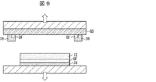
- FIG. 9 is a diagram showing a delamination process according to this embodiment.
- FIG. 10 is a figure which shows the attachment of the lower surface film 10 which concerns on this embodiment.
- a delamination step (peeling step) of peeling the display function layer DF from the glass substrate GS and the dot pattern DP is performed.
- the display function layer DF includes a plurality of display panels, the plurality of display panels are peeled together from the glass substrate GS in the delamination process.
- the delamination process is performed by vacuum adsorption. That is, in this delamination process, in FIG. 9, an upper stage that vacuum-sucks the glass substrate GS by a vacuum suction mechanism (not shown) and a lower stage that vacuum-sucks the upper surface film 39 by a vacuum suction mechanism (not shown) are respectively illustrated.
- the resin layer 12 and the dot pattern DP are physically peeled off by moving in the upward and downward directions indicated by the arrow 9 to peel off the display function layer DF from the glass substrate GS and the dot pattern DP. In FIG. 9, the dot pattern DP remaining on the glass substrate GS is not shown.
- the lower surface film (second lamination film (2nd laminating)) 10 is attached on the resin layer 12 with the adhesive layer 11 interposed.
- the glass substrate GS may be vacuum-sucked on the upper stage and the display function layer DF may be vacuum-sucked on the lower stage.
- the display function layer DF can be peeled from the dot pattern DP by vacuum suction and gravity, and the resin layer 12 of the display function layer DF faces the vertically upper side, so that the lower surface film 10 can be easily attached.
- vacuum suction may be performed while the stage on which the glass substrate GS is placed is inclined.
- the dot pattern DP is set to 10 to 30 ⁇ m.
- the diameter of the dot pattern DP is preferably 20 ⁇ m. The reason is that the glass substrate GS and the resin layer 12 are attached via the dot pattern DP at the time of laser scanning, but are large enough to be peeled off by vacuum suction at the time of delamination.
- the delamination step can be easily performed in a state where the handling property during transportation is improved.
- the handling property even if the laminated body including the resin layer 12 is located below the glass substrate GS, the dot pattern DP exists inside the resin layer 12 before the delamination, so that the resin layer 12 is formed during the delamination. Only fall can be prevented.
- the glass substrate GS may be adsorbed by the lower stage and the above laminated body may be adsorbed by the upper stage.
- the lamination film is attached for the second time, and then the display device 2 is singulated by a CO 2 laser or the like.
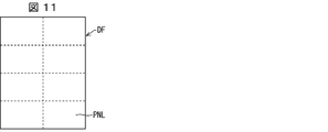
- FIG. 11 is a diagram showing an example of the display function layer DF immediately before the singulation according to the present embodiment.
- the display panels PNL are manufactured, for example, into eight display panels PNL.
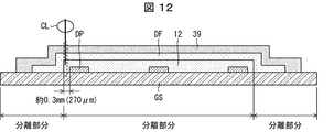
- FIG. 12 is a diagram showing an example of cutting the display function layer and the upper surface film according to the present embodiment.
- the CO 2 laser CL is irradiated between the end portion of the resin layer 12 and the dot pattern DP.
- the width divided by the CO 2 laser CL is 400 ⁇ m, and the positioning error of the CO 2 laser CL is ⁇ 70 ⁇ m. Therefore, when the CO 2 laser CL is irradiated so that the center of the light beam is positioned at the boundary of the separated portion, that is, the end of the resin layer 12, it hits a position 270 (400/2 + 70) ⁇ m inside from the end of the resin layer 12. It will be.
- the dot pattern DP disappears. Therefore, the dot pattern DP is inwardly 0.3 to 0.5 mm from the end of the resin layer 12 with a margin. It is desirable to form.
- a dot pattern is formed for each display panel, and the display functional layer DF and the upper surface film 39 are divided during the dividing step (see FIG. 14). That is, in the case of FIG. 14, the display functional layer DF and the upper surface film 39 are divided by the same CO 2 laser as in the dividing step in Embodiment 1 so that the six display panels are separated. After that, the display function layer DF and the upper surface film 39 are separated into individual display panels in a peeling process from the glass substrate GS (support substrate S).
- FIG. 13 is a flowchart showing an outline of a method of manufacturing the display device 2 according to this embodiment.
- processing different from that of the first embodiment will be described.
- step S106 the display function layer DF and the upper surface film 39 are divided in each of the plurality of display panels formed on the glass substrate GS.
- step S7 ' each display panel is peeled off from each glass substrate GS and dot pattern DP, and the display panels are singulated at the same time. The details will be described below.
- FIG. 14 is a diagram showing a cut of the display function layer and the upper surface film according to the present embodiment.
- the dot pattern DP is formed in units of a plurality of display panels on the glass substrate GS and along the edges of the display panels.
- a dividing step (step S6 ') of cutting the upper surface film 39, the resin layer 12, and the display function layer DF into a frame shape is performed at a position corresponding to the outer periphery of the oval including one display panel. That is, in the dividing step (step S6 '), the resin layer 12 and the display function layer DF are divided for each display panel. Then, when the glass substrate GS and the resin layer 12 and the like are peeled off, the display panel is divided into individual pieces at the same time (step S7 ').
- the dot pattern DP is attached to each divided display panel as described above, a plurality of display panels are peeled off from the glass substrate GS and the dot pattern DP in the delamination process.
- the electro-optical element (electro-optical element whose brightness and transmittance are controlled by current) provided in the display device 2 according to this embodiment is not particularly limited.
- the display device 2 according to the present embodiment include an organic EL (Electro Luminescence) display including an OLED (Organic Light Emitting Diode) as an electro-optical element, and an inorganic light-emitting diode as an electro-optical element.
- Examples thereof include an inorganic EL display provided, and a QLED display provided with a QLED (Quantum dot Light Emitting Diode) as an electro-optical element.
- a method of manufacturing a display device is a method of manufacturing a display device in which a plurality of display panels are collectively formed by using a mother substrate, wherein a plurality of metal shape retention patterns are formed on the mother substrate. And a step of forming a resin layer so as to cover the shape retaining pattern, a step of forming a TFT layer including at least one inorganic insulating film on the resin layer, and a light emitting element layer on the TFT layer. And a step of forming a sealing layer on the light emitting element layer, a resin film, the TFT layer, the light emitting element layer, and a top surface film on the upper surface of the display functional layer including the sealing layer.
- the shape retention pattern is formed along an end of the resin layer
- the display functional layer includes the plurality of display panels
- the plurality of displays from the mother substrate are displayed. Peel the panels together.
- the shape retention pattern is formed on the display panel unit basis and along the edge of the display panel, and in the peeling step, the plurality of display panels are peeled together from the mother substrate.
- the shape retention pattern is formed at a position within 0.5 mm from the end surface of the resin layer.
- the shape retention pattern has a circular shape in a plan view, and the diameter of the circular shape is 10 to 30 ⁇ m.
- the inorganic insulating film includes a base coat film.
- Aspect 7 is the method of manufacturing a display device according to any one of claims 1 to 6, wherein a CO 2 laser is used in the dividing step.
- the peeling step is performed by vacuum suction.
- the mother substrate is vacuum-sucked on the upper stage, and the display function layer is vacuum-sucked on the lower stage.
- vacuum suction is performed while the stage on which the mother substrate is placed is inclined.
- an excimer laser is used in the separation step.
- Display Device 10 Bottom Film 12 Resin Layer 13 Barrier Layer (Inorganic Insulation Film) 14 TFT layer 15 Light emitting element layer 16 Sealing layer 17 First inorganic insulating film (inorganic insulating film) 18 Second inorganic insulating film (inorganic insulating film) 20 Third inorganic insulating film (inorganic insulating film) 39 Top film DP dot pattern (shape retention pattern) DF Display function layer EL excimer laser (laser light) GS glass substrate (mother substrate) PNL display panel
Landscapes
- Engineering & Computer Science (AREA)
- Physics & Mathematics (AREA)
- General Physics & Mathematics (AREA)
- Theoretical Computer Science (AREA)
- Manufacturing & Machinery (AREA)
- Electroluminescent Light Sources (AREA)
Abstract
表示デバイス(2)の製造方法は、ガラス基板(GS)上に複数の金属製のドットパターン(DP)を形成し、ドットパターンを覆うように樹脂層(12)を形成し、樹脂層上に表示機能層(DF)を形成し、表示機能層上に上面フィルム(39)を貼り付け、複数の表示パネルの外周で樹脂層と無機絶縁膜をカットし、ガラス基板側からレーザ光照射でガラス基板から樹脂層を分離し、ガラス基板とドットパターンから表示機能層を剥離する。
Description
本発明は、表示デバイスの製造方法に関する。
従来、フレキシブルOLED(Organic Light Emitting Diode)において、レーザリフトオフ(Laser Lift Off, LLO)工程後にガラス基板GSからOLEDパネル膜(樹脂層)12を分離するデラミ工程(剥離工程)がある。図15に示すように、デラミ工程では、カッターにより上面フィルム39とガラス基板GSとを分離させ、またバリア層13の端部を破壊する。その後、ガラス基板GSとOLEDパネル膜12を分離する。このように、カッターを用いていたので、精度の問題や操作の難しさがある。
そこで、特許文献1には、レーザリフトオフ工程の前に、分断工程を行ってガラス基板GSとOLEDパネル膜12との分離を妨げるバリア層13等の部分を、先に分断することが提案されている。
しかしながら、特許文献1の技術では、レーザリフトオフ工程後において、ガラス基板GSと、OLEDパネル膜12とが完全に分離される。そのため、この従来技術では、その製造途中、例えば、デラミ工程を行う前に、OLEDパネル膜12の形状を保持することができずに、当該OLEDパネル膜12を含んだOLEDパネル(表示デバイス)のハンドリング性が低下するという問題を生じた。
前記の課題を解決するために、本発明の一態様に係る表示デバイスの製造方法は、母基板を用いて複数の表示パネルを一括して形成する、表示デバイスの製造方法であって、母基板上に、複数の金属製の形状保持パターンを形成する工程と、前記形状保持パターンを覆うように樹脂層を形成する工程と、前記樹脂層上に少なくとも1層の無機絶縁膜を含むTFT層を形成する工程と、前記TFT層上に発光素子層を形成する工程と、前記発光素子層上に封止層を形成する工程と、前記樹脂層、前記TFT層、前記発光素子層、および、前記封止層を含む表示機能層の上面に上面フィルムを貼り付ける工程と、前記表示パネルと当該表示パネルの外周とで分離するように、前記表示機能層及び前記上面フィルムを分断する分断工程と、前記母基板側からレーザ光を照射して、当該母基板から前記樹脂層を分離する分離工程と、前記母基板及び前記形状保持パターンから前記表示機能層を剥離する剥離工程と、を含む。
本発明の一態様によれば、製造途中での表示デバイスのハンドリング性を向上させることができる。
〔実施形態1〕
以下、本発明の実施形態1について、詳細に説明する。本実施形態に係る表示デバイスの製造方法は、母基板を用いて複数の表示パネルを一括して形成するものである。特に、大判の母基板(個片化の前)において、複数の表示パネルを含む表示機能層のバリア層、無機絶縁膜等の分断工程を行うものである。
以下、本発明の実施形態1について、詳細に説明する。本実施形態に係る表示デバイスの製造方法は、母基板を用いて複数の表示パネルを一括して形成するものである。特に、大判の母基板(個片化の前)において、複数の表示パネルを含む表示機能層のバリア層、無機絶縁膜等の分断工程を行うものである。
以下においては、「同層」とは同一のプロセスにて形成されていることを意味し、「下層」とは、比較対象の層よりも先のプロセスで形成されていることを意味し、「上層」とは比較対象の層よりも後のプロセスで形成されていることを意味する。
図1は、本実施形態に係る表示デバイス2の上面図である。図2は、図1におけるB-B線矢視断面図である。本実施形態に係る表示デバイス2は、図1に示すように、表示領域DAと、当該表示領域DAの周囲に隣接する額縁領域NAとを有する。額縁領域NAの一端部には、図1に示すように、端子部Tが形成される。端子部Tには、表示領域DAからの接続配線CLを介して表示領域DAにおける各発光素子を駆動するための信号を供給する、図示しないドライバ等が実装される。
ここで、図2を参照して、本実施形態に係る表示デバイス2の、表示領域DAにおける各層の構成を詳細に説明する。図2(a)は、上面フィルム39を含む構成を示す。図2(b)は、機能フィルム40を含む構成を示す。
図2に示すように、本実施形態に係る表示デバイス2は、下層から順に、下面フィルム10と、接着層11と、樹脂層12と、TFT層14と、発光素子層15と、封止層16とを備える。図2(a)に示すように、表示デバイス2は、製造工程の途中において、封止層16のさらに上層に、保護機能を有する上面フィルム39を備えることがある。図2(b)に示すように、表示デバイス2は、製造終了時に、封止層16のさらに上層に、上面フィルム39に代えて、光学補償機能、タッチセンサ機能、保護機能等を有する機能フィルム40を備えていてもよい。
下面フィルム10は、表示デバイス2の基材フィルムであり、例えば、有機樹脂材料を含んでいてもよい。接着層11は、下面フィルム10と樹脂層12とを接着する層であり、従来公知の接着剤を使用して形成してもよい。樹脂層12は、材料としてポリイミド(以下、PIともいう)を含む。
TFT層14は、下層から順に、バリア層13、半導体膜19と、第1無機絶縁膜17(ゲート絶縁膜)と、ゲート電極GEと、第2無機絶縁膜18と、容量電極CEと、第3無機絶縁膜20と、ソース配線SH(金属配線層)と、平坦化膜21(層間絶縁膜)とを含む。半導体膜19と、第1無機絶縁膜17と、ゲート電極GEとを含むように、薄層トランジスタ(TFT)Trが構成される。
バリア層13は、表示デバイス2の使用時に、水、酸素等の異物がTFT層14、発光素子層15に浸透することを防ぐ層である。バリア層13は、例えば、CVDにより形成される、酸化シリコン膜、窒化シリコン膜、あるいは酸窒化シリコン膜、またはこれらの積層膜で構成することができる。
半導体膜19は、例えば低温ポリシリコン(LTPS)あるいは酸化物半導体で構成される。なお、図1においては、半導体膜19をチャネルとするTFTがトップゲート構造で示されているが、ボトムゲート構造であってもよい(例えば、TFTのチャネルが酸化物半導体の場合)。
ゲート電極GE、容量電極CE、またはソース配線SHは、例えば、アルミニウム(Al)、タングステン(W)、モリブデン(Mo)、タンタル(Ta)、クロム(Cr)、チタン(Ti)、銅(Cu)の少なくとも1つを含んでいてもよい。すなわち、ゲート電極GE、容量電極CE、またはソース配線SHは、上述の金属の単層膜あるいは積層膜によって構成される。
第1無機絶縁膜17、第2無機絶縁膜18、および第3無機絶縁膜20は、例えば、CVD法によって形成された、酸化シリコン(SiOx)膜あるいは窒化シリコン(SiNx)膜またはこれらの積層膜によって構成することができる。
平坦化膜21は、例えば、ポリイミド、アクリル等の塗布可能な感光性有機材料によって構成することができる。
発光素子層15(例えば、有機発光ダイオード層)は、下層から順に、画素電極22(第1電極、例えばアノード)と、画素電極22のエッジを覆うカバー膜(エッジカバー)23と、機能層24と、上部電極(第2電極、例えばカソード)25とを含む。発光素子層15は、サブピクセルSP(画素)ごとに、島状の画素電極22、島状の機能層24、および上部電極25を含む発光素子(例えば、OLED:有機発光ダイオード)と、これを駆動するサブ画素回路とが設けられる。また、TFT層14において、当該サブ画素回路ごとにトランジスタTrが形成され、トランジスタTrの制御をもって、サブ画素回路が制御される。
画素電極22は、平面視において、平坦化膜21と当該平坦化膜21の開口であるコンタクトホールとに重畳する位置に設けられる。画素電極22は、コンタクトホールを介してソース配線SHと電気的に接続される。このため、TFT層14における信号が、ソース配線SHを介して画素電極22に供給される。なお、画素電極22の厚みは、例えば、2nmであってもよい。
画素電極22は、複数のサブピクセルSPごとに島状に形成され、例えばITO(Indium Tin Oxide)とAgを含む合金との積層によって構成され、光反射性を有する。上部電極25は、複数のサブピクセルSPの共通層としてベタ状に形成され、ITO(Indium Tin Oxide)、IZO(Indium Zinc Oxide)等の透光性の導電材によって構成することができる。
カバー膜23は有機絶縁膜であり、画素電極22のエッジを覆う位置に形成され、複数のサブピクセルSPごとに開口23cを備え、画素電極22の一部が露出する。カバー膜23は、例えば、ポリイミド等の塗布可能な材料によって構成することができる。
機能層24は、例えば、下層側から順に、正孔輸送層、発光層、電子輸送層を積層することで構成されており、実質的に光を発光する層である。本実施形態においては、機能層24の少なくとも1層は、蒸着法によって形成される。また、本実施形態においては、機能層24の各層は、サブピクセルSPごとに島状に形成されていてもよく、複数のサブピクセルSPの共通層としてベタ状に形成されていてもよい。
発光素子層15がOLED層である場合、画素電極22および上部電極25間の駆動電流によって正孔と電子が上記発光層内で再結合し、これによって生じたエキシトンが基底状態に落ちることによって、光が放出される。上部電極25が透光性を有し、画素電極22が光反射性を有するため、機能層24から放出された光は上方に向かい、トップエミッションとなる。
封止層16は、上部電極25よりも上層の第1無機封止膜26と、第1無機封止膜26よりも上層の有機封止膜27と、有機封止膜27よりも上層の第2無機封止膜28とを含み、水、酸素等の異物の発光素子層15への浸透を防ぐ。第1無機封止膜26および第2無機封止膜28は、例えば、CVDにより形成される、酸化シリコン膜、窒化シリコン膜、あるいは酸窒化シリコン膜、またはこれらの積層膜で構成することができる。有機封止膜27は、ポリイミド、アクリル等の塗布可能な感光性有機材料によって構成することができる。
本実施形態に係る表示デバイスの製造方法の概要について、図3のフローチャートを参照して詳細に説明する。図3は、表示デバイス2の製造方法の概要を示すフローチャートである。
はじめに、例えば、透光性のマザーガラス基板である、支持基板S上に、形状保持パターンの一例であるドットパターンDPおよび樹脂層12を形成する(ステップS1)。形状保持パターンは、樹脂層12の形状を保持するためのものである。次いで、樹脂層12の上層にTFT層14を形成する(ステップS2)。この際、端子部Tおよび接続配線CLを形成してもよい。
次いで、トップエミッション型の発光素子層(例えば、OLED素子層)15を形成する(ステップS3)。ステップS3においては、発光素子層15の各層を従来公知の手法により形成してもよく、特に、機能層24を、蒸着法等により形成してもよい。次いで、封止層16を形成する(ステップS4)。
次いで、封止層16の上面に、上面フィルム39を貼り付ける(ステップS5)。上面フィルム39は、封止層16の上面に貼り付けられ、下面フィルム10と同一の材料からなっていてもよい。上面フィルム39は、下面フィルム10と同様に、接着層を介して封止層16に貼り付けられていてもよい。
次いで、表示機能層DFおよび上面フィルム39を分断する(ステップS6)。ステップS6においては、無機絶縁膜等の分断と、個片化とは、同じタイミングで行ってもよいし、別々に行ってもよい。
次いで、支持基板Sを樹脂層12から剥離する(ステップS7)。支持基板Sの剥離は、例えば、支持基板S越しに樹脂層12の下面にレーザ光を照射して、支持基板Sと樹脂層12との結合力を低下させ、支持基板Sを樹脂層12から剥離する手法により実行してもよい。
次いで、下面フィルム10を、接着層11を介して、各構造体の下面に貼り付ける(ステップS8)。次いで、下面フィルム10から上面フィルム39までの積層体を分断し、個片化する(ステップS9)。次いで、上面フィルム39を封止層16から剥離した後、機能フィルム40を、個片化した各積層体の上面に貼り付ける(ステップS10)。次いで、端子部Tに電子回路基板(例えば、ICチップ)をマウントし、表示デバイス2とする(ステップS11)。
本実施形態に係る表示デバイスの製造方法の詳細について、図4~10を参照して詳細に説明する。
(ドットパターン配置)
図4は、本実施形態に係るドットパターン配置を示す図である。図4(a)は上面図を示し、図4(b)は側断面図を示す。図4に示すように、まず、ガラス基板(母基板)GS上に、複数の金属(例えば、モリブデン(Mo)等)製のドットからなるドットパターンDPを形成する工程が行われる。当該ドットパターンDPは、上述したように、形状保持パターンの一例であり、ガラス基板GSの上面のうち、塗布予定領域PAにスパッタ、蒸着等により形成される。本実施形態では、ドットパターンDPは、ガラス基板GS全体において配置される。この場合、個片化工程は、2回目に下面フィルム(ラミネーションフィルム)10を貼る工程の後に実施される。
図4は、本実施形態に係るドットパターン配置を示す図である。図4(a)は上面図を示し、図4(b)は側断面図を示す。図4に示すように、まず、ガラス基板(母基板)GS上に、複数の金属(例えば、モリブデン(Mo)等)製のドットからなるドットパターンDPを形成する工程が行われる。当該ドットパターンDPは、上述したように、形状保持パターンの一例であり、ガラス基板GSの上面のうち、塗布予定領域PAにスパッタ、蒸着等により形成される。本実施形態では、ドットパターンDPは、ガラス基板GS全体において配置される。この場合、個片化工程は、2回目に下面フィルム(ラミネーションフィルム)10を貼る工程の後に実施される。
なお、形状保持パターンは、図4(a)に示した、平面視で円形状のドットパターンに限定されるものではなく、例えば、平面視で三角形状および矩形状を含む多角形状のパターンであってもよいし、楕円形状等の他形状のパターンであってもよい。
塗布予定領域PAは、樹脂層12が形成される予定の領域であり、例えば、PIが塗布される予定の領域である。ドットパターンDPは、樹脂層12の端面から0.5mm(好ましくは0.3mm)以内の位置に形成される。ドットパターンDPは、直径10~30μm(例えば、20μmであってもよい)である。
(PI塗布、および、バリア層デポ)
図5は、本実施形態に係るPI塗布、および、バリア層デポを示す図である。図5(a)は上面図を示し、図5(b)は側断面図を示す。図5に示すように、図4に続いて、ドットパターンDPを覆うように樹脂層12を形成する工程が行われる。図5(a)に示すように、ドットパターンDPは、樹脂層12の端部に沿うように少なくとも樹脂層12の四隅に形成される。なお、ドットパターンDPの厚さは例えば200nmであり、樹脂層12の厚さは例えば12μmである。
図5は、本実施形態に係るPI塗布、および、バリア層デポを示す図である。図5(a)は上面図を示し、図5(b)は側断面図を示す。図5に示すように、図4に続いて、ドットパターンDPを覆うように樹脂層12を形成する工程が行われる。図5(a)に示すように、ドットパターンDPは、樹脂層12の端部に沿うように少なくとも樹脂層12の四隅に形成される。なお、ドットパターンDPの厚さは例えば200nmであり、樹脂層12の厚さは例えば12μmである。
そして、図2に示すように、樹脂層12上に少なくとも1層の無機絶縁膜を含むTFT層14(少なくとも1層の無機絶縁膜は、バリア層13、第1無機絶縁膜17、第2無機絶縁膜18、第3無機絶縁膜20を含む)を形成する工程と、TFT層14上に発光素子層15を形成する工程と、発光素子層15上に封止層16を形成する工程とが行われる。なお、少なくとも一層の無機絶縁膜は、樹脂層12の表面とその端部を覆うように形成される(図5にはバリア層13のみ図示)。
表示デバイス2は、周縁部に、複数の金属製のドットからなるドットパターンDPが形成されたガラス基板GSと、ドットパターンDPを覆うように形成された樹脂層12と、樹脂層12上に形成された、少なくとも1層の無機絶縁膜を含むTFT層14と、TFT層14上に形成された発光素子層15と、を備えている。なお、無機絶縁膜には、ベースコート膜が含まれる。
(上面フィルムの貼り付け)
図6は、本実施形態に係る上面フィルムの貼り付けを示す図である。図6(a)は上面図を示し、図6(b)は側断面図を示す。図6に示すように、図5に続いて、樹脂層12、および、表示機能層DFの上面に上面フィルム(1回目のラミネーションフィルム(1stラミ))39を貼り付ける工程が行われる。なお、図6~10、13において、樹脂層12と、表示機能層DFとは、別個に図示している。本来は、図2に示すように、表示機能層DFは、樹脂層12、TFT層14、発光素子層15、および、封止層16を含む。従って、上記の工程は、樹脂層12、TFT層14、発光素子層15、および、封止層16を含む表示機能層DFの上面に上面フィルム39を貼り付ける工程であると言える。本実施形態では、表示機能層DFは、複数の表示パネルPNLを含む(図11参照)。
図6は、本実施形態に係る上面フィルムの貼り付けを示す図である。図6(a)は上面図を示し、図6(b)は側断面図を示す。図6に示すように、図5に続いて、樹脂層12、および、表示機能層DFの上面に上面フィルム(1回目のラミネーションフィルム(1stラミ))39を貼り付ける工程が行われる。なお、図6~10、13において、樹脂層12と、表示機能層DFとは、別個に図示している。本来は、図2に示すように、表示機能層DFは、樹脂層12、TFT層14、発光素子層15、および、封止層16を含む。従って、上記の工程は、樹脂層12、TFT層14、発光素子層15、および、封止層16を含む表示機能層DFの上面に上面フィルム39を貼り付ける工程であると言える。本実施形態では、表示機能層DFは、複数の表示パネルPNLを含む(図11参照)。
なお、ガラス基板GSの上面のうち、樹脂層12の端面よりも外側にある、バリア層13および上面フィルム39(図6(b)の破線が示す箇所)は、デラミ工程の妨げになる。
(表示機能層、および上面フィルムのカット)
図7は、本実施形態に係る表示機能層、および上面フィルムのカットを示す図である。図7(a)は上面図を示し、図7(b)は側断面図を示す。図7に示すように、図6に続いて、表示パネルPNLと表示パネルPNLの外周とで分離するように、表示機能層DF、および上面フィルム39を枠状にカットする分断工程が行われる。分断工程においては、CO2レーザCLを用いる。カットされる幅は、例えば、100~400μmである。
図7は、本実施形態に係る表示機能層、および上面フィルムのカットを示す図である。図7(a)は上面図を示し、図7(b)は側断面図を示す。図7に示すように、図6に続いて、表示パネルPNLと表示パネルPNLの外周とで分離するように、表示機能層DF、および上面フィルム39を枠状にカットする分断工程が行われる。分断工程においては、CO2レーザCLを用いる。カットされる幅は、例えば、100~400μmである。
本実施形態に係る分断工程では、図7(b)に示すように、ガラス基板GSはカットされず、表示デバイス2の個片化は行われない。なお、本実施形態に係る個片化は、デラミ工程の後に行われる。
(レーザリフトオフ)
図8は、本実施形態に係るレーザリフトオフ工程を示す図である。図8(a)は上面図を示し、図8(b)は側断面図を示す。図8に示すように、図7に続いて、個片化される前のガラス基板GS側からレーザ光を照射して、ガラス基板GSから樹脂層12を分離する分離工程(LLO工程)が行われる。分離工程においては、エキシマレーザ(レーザ光)ELを用いる。エキシマレーザELのパワーは、例えば、180mJ/cm2である。
図8は、本実施形態に係るレーザリフトオフ工程を示す図である。図8(a)は上面図を示し、図8(b)は側断面図を示す。図8に示すように、図7に続いて、個片化される前のガラス基板GS側からレーザ光を照射して、ガラス基板GSから樹脂層12を分離する分離工程(LLO工程)が行われる。分離工程においては、エキシマレーザ(レーザ光)ELを用いる。エキシマレーザELのパワーは、例えば、180mJ/cm2である。
本実施形態に係る分離工程では、ガラス基板GSと、樹脂層12とが密着しなくなった状態であって、まだ引き離されていない状態であり、ドットパターンDPがガラス基板GS上に残る。ここで、例えば、直径10~30μmのドットパターンDPがあるので、樹脂層12の形状は維持されるとともに、ドットパターンDPのない部分の樹脂層12はガラス基板GSから分離される。
実際には、図8(b)に示すように、ガラス基板GSを上側にした状態で、ガラス基板GSの上方から下方に向けてエキシマレーザELを照射する。なお、この説明に限ることなく、ガラス基板GSを下側にした状態で、ガラス基板GSの下方から上方に向けてエキシマレーザELを照射してもよい。
(デラミ)
図9は、本実施形態に係るデラミ工程を示す図である。図10は、本実施形態に係る下面フィルム10の貼り付けを示す図である。
図9は、本実施形態に係るデラミ工程を示す図である。図10は、本実施形態に係る下面フィルム10の貼り付けを示す図である。
図9に示すように、図8に続いて、ガラス基板GS及びドットパターンDPから表示機能層DFを剥離するデラミ工程(剥離工程)が行われる。本実施形態においては表示機能層DFが複数の表示パネルを含むので、デラミ工程において、ガラス基板GSから複数の表示パネルをともに剥離する。
また、デラミ工程は、真空吸着により行われる。すなわち、このデラミ工程では、図9において、図略の真空吸着機構によってガラス基板GSを真空吸着した上側ステージ、及び図略の真空吸着機構によって上面フィルム39を真空吸着した下側ステージを、それぞれ図9の矢印が示す上方向及び下方向に移動させることにより、樹脂層12とドットパターンDPとを物理的に剥がして、ガラス基板GS及びドットパターンDPから表示機能層DFを剥離する。なお、図9では、ガラス基板GS上に残ったドットパターンDPの図示は省略している。
図10に示すように、デラミ工程の後に、樹脂層12上に、接着層11を介在させて、下面フィルム(2回目のラミネーションフィルム(2ndラミ))10を貼り付ける。デラミ工程において、図9に示すように、上ステージにガラス基板GSを真空吸着し、下ステージに表示機能層DFを真空吸着してもよい。これによれば、真空吸着および重力によりドットパターンDPから表示機能層DFを剥離することができるし、表示機能層DFの樹脂層12が鉛直上側を向くので、下面フィルム10を貼り易い。また、デラミ工程において、ガラス基板GSを載置したステージを斜めに傾斜させながら真空吸着を行ってもよい。
デラミ工程において、ドットパターンDPが直径50μm以上の場合ではPI剥がれが生じたケースが存在し、30μm未満の場合ではPI剥がれが発生せず、10μm未満では形状の保持が難しい。これらにより、ドットパターンDPを10~30μmとする。
なお、ドットパターンDPの直径は、20μmが好ましい。その根拠は、ドットパターンDPを介して、ガラス基板GSと、樹脂層12とが、レーザスキャンの際には付いているが、デラミの際には真空吸引で剥がれる大きさだからである。
このようなドットパターン(形状保持パターン)DPの形成により、デラミ工程を行い易くすることができる。すなわち、本実施形態では、上記従来例と異なり、搬送途中におけるハンドリング性を向上させた状態で、デラミ工程を容易に行うことが可能になる。ハンドリング性に関しては、樹脂層12を含む積層体をガラス基板GSより下側にしても、デラミの前にはドットパターンDPが樹脂層12内に存在しているので、デラミの途中で樹脂層12のみの落下を防止することができる。
なお、図9とは逆に、ガラス基板GSを下ステージで吸着し、上記の積層体を上ステージで吸着してもよい。本実施形態では、上記のデラミ工程の後に、2回目のラミネーションフィルムの貼り付けを行った上で、CO2レーザ等により表示デバイス2の個片化が行われる。
(実施例)
図11は、本実施形態に係る個片化直前の表示機能層DFの一例を示す図である。図9に示すデラミ(剥離)工程(図3のステップS7)、および、下面フィルム10の貼り付け工程(図3のステップS8)の後に、図11に示すように、表示機能層DFが分断により個片化されて、例えば、8個の表示パネルPNLが製造される。
図11は、本実施形態に係る個片化直前の表示機能層DFの一例を示す図である。図9に示すデラミ(剥離)工程(図3のステップS7)、および、下面フィルム10の貼り付け工程(図3のステップS8)の後に、図11に示すように、表示機能層DFが分断により個片化されて、例えば、8個の表示パネルPNLが製造される。
図12は、本実施形態に係る表示機能層、および上面フィルムのカットの実施例を示す図である。図12に示すように、CO2レーザCLは、樹脂層12の端部と、ドットパターンDPとの間に照射される。CO2レーザCLで分断される幅は400μm、CO2レーザCLの位置決め誤差は±70μmである。従って、分離部分の境界、すなわち、樹脂層12の端部に光線の中心が位置付くようにCO2レーザCLを照射すると、樹脂層12の端部から270(400/2+70)μm内側の箇所に当たることになる。
そこで、CO2レーザCLが金属製のドットパターンDPに当たると、ドットパターンDPが消失するので、マージンを以って樹脂層12の端部から0.3~0.5mmだけ内側にドットパターンDPを形成するのが望ましい。
〔実施形態2〕
本発明の実施形態2について、以下に説明する。なお、説明の便宜上、実施形態1にて説明した部材と同じ機能を有する部材については、同じ符号を付記し、その説明を繰り返さない。本実施形態では、表示パネル単位に、ドットパターンを形成して、分断工程(図14参照)の際に、表示機能層DF及び上面フィルム39を分断する。つまり、図14の場合には、6個の表示パネルがばらばらとなるように、実施形態1における分断工程と同じCO2レーザで表示機能層DF及び上面フィルム39を分断する。その後、表示機能層DF及び上面フィルム39は、ガラス基板GS(支持基板S)との剥離工程において、表示パネル単位に個片化される。
本発明の実施形態2について、以下に説明する。なお、説明の便宜上、実施形態1にて説明した部材と同じ機能を有する部材については、同じ符号を付記し、その説明を繰り返さない。本実施形態では、表示パネル単位に、ドットパターンを形成して、分断工程(図14参照)の際に、表示機能層DF及び上面フィルム39を分断する。つまり、図14の場合には、6個の表示パネルがばらばらとなるように、実施形態1における分断工程と同じCO2レーザで表示機能層DF及び上面フィルム39を分断する。その後、表示機能層DF及び上面フィルム39は、ガラス基板GS(支持基板S)との剥離工程において、表示パネル単位に個片化される。
図13は、本実施形態に係る表示デバイス2の製造方法の概要を示すフローチャートである。ここでは、実施形態1(図3のフローチャート)と異なる処理について説明する。ステップS106においては、ガラス基板GS上に形成された、複数の各表示パネルにおいて、表示機能層DF及び上面フィルム39を分断する。その後、ステップS7’において、各表示パネルを、それぞれのガラス基板GSおよびドットパターンDPから剥離して、表示パネルの個片化が同時に行われる。以下に、詳細を説明する。
図14は、本実施形態に係る表示機能層、および上面フィルムのカットを示す図である。図14に示すように、ドットパターンDPは、ガラス基板GS上の複数の表示パネル単位に、かつ、表示パネルの端部に沿うように形成される。そして、1つの表示パネルを含む小判の外周に対応する位置で、上面フィルム39、樹脂層12および表示機能層DFを枠状にカットする分断工程(ステップS6’)が行われる。すなわち、当該分断工程(ステップS6’)においては、表示パネル単位に、樹脂層12と、表示機能層DFとが分断される。そして、ガラス基板GSと、樹脂層12等との剥離が行われると、同時に表示パネルの個片化が行われる(ステップS7’)。
なお、上記により、分断された表示パネルごとにドットパターンDPが着いているので、デラミ工程においては、ガラス基板GSおよびドットパターンDPから複数の表示パネルを剥離する。
〔まとめ〕
本実施形態にかかる表示デバイス2が備える電気光学素子(電流によって輝度や透過率が制御される電気光学素子)は特に限定されるものではない。本実施形態にかかる表示デバイス2としては、例えば、電気光学素子としてOLED(Organic Light Emitting Diode:有機発光ダイオード)を備えた有機EL(Electro Luminescence:エレクトロルミネッセンス)ディスプレイ、電気光学素子として無機発光ダイオードを備えた無機ELディスプレイ、電気光学素子としてQLED(Quantum dot Light Emitting Diode:量子ドット発光ダイオード)を備えたQLEDディスプレイ等が挙げられる。
本実施形態にかかる表示デバイス2が備える電気光学素子(電流によって輝度や透過率が制御される電気光学素子)は特に限定されるものではない。本実施形態にかかる表示デバイス2としては、例えば、電気光学素子としてOLED(Organic Light Emitting Diode:有機発光ダイオード)を備えた有機EL(Electro Luminescence:エレクトロルミネッセンス)ディスプレイ、電気光学素子として無機発光ダイオードを備えた無機ELディスプレイ、電気光学素子としてQLED(Quantum dot Light Emitting Diode:量子ドット発光ダイオード)を備えたQLEDディスプレイ等が挙げられる。
態様1の表示デバイスの製造方法は、母基板を用いて複数の表示パネルを一括して形成する、表示デバイスの製造方法であって、母基板上に、複数の金属製の形状保持パターンを形成する工程と、前記形状保持パターンを覆うように樹脂層を形成する工程と、前記樹脂層上に少なくとも1層の無機絶縁膜を含むTFT層を形成する工程と、前記TFT層上に発光素子層を形成する工程と、前記発光素子層上に封止層を形成する工程と、前記樹脂層、前記TFT層、前記発光素子層、および、前記封止層を含む表示機能層の上面に上面フィルムを貼り付ける工程と、前記表示パネルと当該表示パネルの外周とで分離するように、前記表示機能層及び前記上面フィルムを分断する分断工程と、前記母基板側からレーザ光を照射して、当該母基板から前記樹脂層を分離する分離工程と、前記母基板及び前記形状保持パターンから前記表示機能層を剥離する剥離工程と、を含む表示デバイスの製造方法。
態様2では、前記形状保持パターンは、前記樹脂層の端部に沿うように形成され、前記表示機能層は、前記複数の表示パネルを含み、前記剥離工程において、前記母基板から前記複数の表示パネルをともに剥離する。
態様3では、前記形状保持パターンは、前記表示パネル単位に、かつ、当該表示パネルの端部に沿うように形成され、前記剥離工程において、前記母基板から前記複数の表示パネルをともに剥離する。
態様4では、前記形状保持パターンは、前記樹脂層の端面から0.5mm以内の位置に形成される。
態様5では、前記形状保持パターンは、平面視で円形の形状を有し、当該円形の直径10~30μmである。
態様6では、前記無機絶縁膜には、ベースコート膜が含まれる。
態様7では、前記分断工程において、CO2レーザを用いる、請求項1~6の何れか1項に記載の表示デバイスの製造方法。
態様8では、前記剥離工程は、真空吸着により行う。
態様9では、前記剥離工程の後に、前記樹脂層上に下面フィルムを貼り付ける。
態様10では、前記剥離工程において、上ステージに前記母基板を真空吸着し、下ステージに前記表示機能層を真空吸着する。
態様11では、前記剥離工程において、上記母基板を載置したステージを斜めに傾斜させながら真空吸着を行う。
態様12では、上記分離工程において、エキシマレーザを用いる。
本発明は上述した各実施形態に限定されるものではなく、請求項に示した範囲で種々の変更が可能であり、異なる実施形態にそれぞれ開示された技術的手段を適宜組み合わせて得られる実施形態についても本発明の技術的範囲に含まれる。さらに、各実施形態にそれぞれ開示された技術的手段を組み合わせることにより、新しい技術的特徴を形成することができる。
2 表示デバイス
10 下面フィルム
12 樹脂層
13 バリア層(無機絶縁膜)
14 TFT層
15 発光素子層
16 封止層
17 第1無機絶縁膜(無機絶縁膜)
18 第2無機絶縁膜(無機絶縁膜)
20 第3無機絶縁膜(無機絶縁膜)
39 上面フィルム
DP ドットパターン(形状保持パターン)
DF 表示機能層
EL エキシマレーザ(レーザ光)
GS ガラス基板(母基板)
PNL 表示パネル
10 下面フィルム
12 樹脂層
13 バリア層(無機絶縁膜)
14 TFT層
15 発光素子層
16 封止層
17 第1無機絶縁膜(無機絶縁膜)
18 第2無機絶縁膜(無機絶縁膜)
20 第3無機絶縁膜(無機絶縁膜)
39 上面フィルム
DP ドットパターン(形状保持パターン)
DF 表示機能層
EL エキシマレーザ(レーザ光)
GS ガラス基板(母基板)
PNL 表示パネル
Claims (12)
- 母基板を用いて複数の表示パネルを一括して形成する、表示デバイスの製造方法であって、
母基板上に、複数の金属製の形状保持パターンを形成する工程と、
前記形状保持パターンを覆うように樹脂層を形成する工程と、
前記樹脂層上に少なくとも1層の無機絶縁膜を含むTFT層を形成する工程と、
前記TFT層上に発光素子層を形成する工程と、
前記発光素子層上に封止層を形成する工程と、
前記樹脂層、前記TFT層、前記発光素子層、および、前記封止層を含む表示機能層の上面に上面フィルムを貼り付ける工程と、
前記表示パネルと当該表示パネルの外周とで分離するように、前記表示機能層及び前記上面フィルムを分断する分断工程と、
前記母基板側からレーザ光を照射して、当該母基板から前記樹脂層を分離する分離工程と、
前記母基板及び前記形状保持パターンから前記表示機能層を剥離する剥離工程と、
を含む表示デバイスの製造方法。 - 前記形状保持パターンは、前記樹脂層の端部に沿うように形成され、
前記表示機能層は、前記複数の表示パネルを含み、
前記剥離工程において、前記母基板から前記複数の表示パネルをともに剥離する、請求項1に記載の表示デバイスの製造方法。 - 前記形状保持パターンは、前記表示パネル単位に、かつ、当該表示パネルの端部に沿うように形成され、
前記剥離工程において、前記母基板から前記複数の表示パネルをともに剥離する、請求項1に記載の表示デバイスの製造方法。 - 前記形状保持パターンは、前記樹脂層の端面から0.5mm以内の位置に形成される、請求項1~3の何れか1項に記載の表示デバイスの製造方法。
- 前記形状保持パターンは、平面視で円形の形状を有し、当該円形の直径は10~30μmである、請求項1~4の何れか1項に記載の表示デバイスの製造方法。
- 前記無機絶縁膜には、ベースコート膜が含まれる、請求項1~5の何れか1項に記載の表示デバイスの製造方法。
- 前記分断工程において、CO2レーザを用いる、請求項1~6の何れか1項に記載の表示デバイスの製造方法。
- 前記剥離工程は、真空吸着により行う、請求項1~7の何れか1項に記載の表示デバイスの製造方法。
- 前記剥離工程の後に、前記樹脂層上に下面フィルムを貼り付ける、請求項8に記載の表示デバイスの製造方法。
- 前記剥離工程において、上ステージに前記母基板を真空吸着し、下ステージに前記表示機能層を真空吸着する、請求項9に記載の表示デバイスの製造方法。
- 前記剥離工程において、上記母基板を載置したステージを斜めに傾斜させながら真空吸着を行う、請求項9に記載の表示デバイスの製造方法。
- 上記分離工程において、エキシマレーザを用いる、請求項1~11の何れか1項に記載の表示デバイスの製造方法。
Priority Applications (1)
| Application Number | Priority Date | Filing Date | Title |
|---|---|---|---|
| PCT/JP2018/040593 WO2020090053A1 (ja) | 2018-10-31 | 2018-10-31 | 表示デバイスの製造方法 |
Applications Claiming Priority (1)
| Application Number | Priority Date | Filing Date | Title |
|---|---|---|---|
| PCT/JP2018/040593 WO2020090053A1 (ja) | 2018-10-31 | 2018-10-31 | 表示デバイスの製造方法 |
Publications (1)
| Publication Number | Publication Date |
|---|---|
| WO2020090053A1 true WO2020090053A1 (ja) | 2020-05-07 |
Family
ID=70463631
Family Applications (1)
| Application Number | Title | Priority Date | Filing Date |
|---|---|---|---|
| PCT/JP2018/040593 WO2020090053A1 (ja) | 2018-10-31 | 2018-10-31 | 表示デバイスの製造方法 |
Country Status (1)
| Country | Link |
|---|---|
| WO (1) | WO2020090053A1 (ja) |
Citations (6)
| Publication number | Priority date | Publication date | Assignee | Title |
|---|---|---|---|---|
| JPS645073B2 (ja) * | 1982-11-09 | 1989-01-27 | Sumitomo Chemical Co | |
| US20100124635A1 (en) * | 2008-11-18 | 2010-05-20 | Tae-Woong Kim | Method of Manufacturing Electronic Apparatus including Plastic Substrate, Electronic Apparatus Manufactured Using the Method, and Apparatus for Use in the Method |
| CN103531715A (zh) * | 2013-03-26 | 2014-01-22 | Tcl集团股份有限公司 | 柔性光电器件衬底、柔性光电器件及制备方法 |
| JP2014048619A (ja) * | 2012-09-04 | 2014-03-17 | Panasonic Corp | フレキシブルデバイスの製造方法 |
| US20160254464A1 (en) * | 2014-06-30 | 2016-09-01 | Boe Technology Group Co., Ltd. | Motherboard of flexible display panel and method for manufacturing flexible display panel |
| US20160365522A1 (en) * | 2015-06-10 | 2016-12-15 | Samsung Display Co., Ltd. | Flexible display and method of manufacturing the same |
-
2018
- 2018-10-31 WO PCT/JP2018/040593 patent/WO2020090053A1/ja active Application Filing
Patent Citations (6)
| Publication number | Priority date | Publication date | Assignee | Title |
|---|---|---|---|---|
| JPS645073B2 (ja) * | 1982-11-09 | 1989-01-27 | Sumitomo Chemical Co | |
| US20100124635A1 (en) * | 2008-11-18 | 2010-05-20 | Tae-Woong Kim | Method of Manufacturing Electronic Apparatus including Plastic Substrate, Electronic Apparatus Manufactured Using the Method, and Apparatus for Use in the Method |
| JP2014048619A (ja) * | 2012-09-04 | 2014-03-17 | Panasonic Corp | フレキシブルデバイスの製造方法 |
| CN103531715A (zh) * | 2013-03-26 | 2014-01-22 | Tcl集团股份有限公司 | 柔性光电器件衬底、柔性光电器件及制备方法 |
| US20160254464A1 (en) * | 2014-06-30 | 2016-09-01 | Boe Technology Group Co., Ltd. | Motherboard of flexible display panel and method for manufacturing flexible display panel |
| US20160365522A1 (en) * | 2015-06-10 | 2016-12-15 | Samsung Display Co., Ltd. | Flexible display and method of manufacturing the same |
Similar Documents
| Publication | Publication Date | Title |
|---|---|---|
| JPWO2018179168A1 (ja) | 表示デバイス、表示デバイスの製造方法、表示デバイスの製造装置、成膜装置 | |
| WO2019146115A1 (ja) | 表示デバイスおよび表示デバイスの製造方法 | |
| WO2015030124A1 (ja) | トップエミッション型有機エレクトロルミネッセンス表示装置およびその製造方法 | |
| WO2018179332A1 (ja) | 表示デバイス、表示デバイスの製造方法、表示デバイスの製造装置 | |
| WO2018179132A1 (ja) | 表示デバイスの製造方法、表示デバイス、表示デバイスの製造装置、成膜装置 | |
| KR102169862B1 (ko) | 유기발광다이오드 표시장치 및 이의 제조방법 | |
| WO2018179133A1 (ja) | 表示デバイス、表示デバイスの製造方法、表示デバイスの製造装置、成膜装置、コントローラ | |
| WO2019186845A1 (ja) | 表示装置及び表示装置の製造方法 | |
| WO2018179216A1 (ja) | Elデバイスの製造方法 | |
| KR100496578B1 (ko) | 일렉트로 루미네센스 표시 장치의 제조 방법 | |
| WO2018179201A1 (ja) | 吸着装置、運搬装置、elデバイス製造装置 | |
| JP2019020509A (ja) | 表示装置および表示装置の製造方法 | |
| KR100796128B1 (ko) | 유기 전계 발광표시장치의 제조방법 | |
| WO2020090053A1 (ja) | 表示デバイスの製造方法 | |
| WO2020021722A1 (ja) | 表示デバイスの製造方法 | |
| WO2019069352A1 (ja) | 表示デバイスの製造方法、表示デバイスの製造装置 | |
| WO2018179266A1 (ja) | Elデバイスの製造方法及びelデバイスの製造装置 | |
| KR20160096997A (ko) | 유기발광다이오드 표시장치 및 그 제조방법 | |
| WO2020065966A1 (ja) | 電子デバイスの製造方法 | |
| WO2019038884A1 (ja) | 表示装置 | |
| JP2018160314A (ja) | 表示装置の製造方法 | |
| WO2019030819A1 (ja) | Elデバイスの製造方法 | |
| WO2020031365A1 (ja) | 表示デバイスの製造方法、表示デバイスの製造装置 | |
| US11856835B2 (en) | Method for manufacturing display device | |
| WO2019186902A1 (ja) | 蒸着マスク、および、蒸着マスクの製造方法 |
Legal Events
| Date | Code | Title | Description |
|---|---|---|---|
| 121 | Ep: the epo has been informed by wipo that ep was designated in this application |
Ref document number: 18938604 Country of ref document: EP Kind code of ref document: A1 |
|
| NENP | Non-entry into the national phase |
Ref country code: DE |
|
| 122 | Ep: pct application non-entry in european phase |
Ref document number: 18938604 Country of ref document: EP Kind code of ref document: A1 |
|
| NENP | Non-entry into the national phase |
Ref country code: JP |