WO2020085402A1 - 顕微鏡及び顕微法 - Google Patents
顕微鏡及び顕微法 Download PDFInfo
- Publication number
- WO2020085402A1 WO2020085402A1 PCT/JP2019/041575 JP2019041575W WO2020085402A1 WO 2020085402 A1 WO2020085402 A1 WO 2020085402A1 JP 2019041575 W JP2019041575 W JP 2019041575W WO 2020085402 A1 WO2020085402 A1 WO 2020085402A1
- Authority
- WO
- WIPO (PCT)
- Prior art keywords
- light
- illumination
- electric field
- sample
- unit
- Prior art date
- Legal status (The legal status is an assumption and is not a legal conclusion. Google has not performed a legal analysis and makes no representation as to the accuracy of the status listed.)
- Ceased
Links
Images





Classifications
-
- G—PHYSICS
- G01—MEASURING; TESTING
- G01N—INVESTIGATING OR ANALYSING MATERIALS BY DETERMINING THEIR CHEMICAL OR PHYSICAL PROPERTIES
- G01N21/00—Investigating or analysing materials by the use of optical means, i.e. using sub-millimetre waves, infrared, visible or ultraviolet light
- G01N21/17—Systems in which incident light is modified in accordance with the properties of the material investigated
-
- G—PHYSICS
- G01—MEASURING; TESTING
- G01N—INVESTIGATING OR ANALYSING MATERIALS BY DETERMINING THEIR CHEMICAL OR PHYSICAL PROPERTIES
- G01N21/00—Investigating or analysing materials by the use of optical means, i.e. using sub-millimetre waves, infrared, visible or ultraviolet light
- G01N21/17—Systems in which incident light is modified in accordance with the properties of the material investigated
- G01N21/41—Refractivity; Phase-affecting properties, e.g. optical path length
- G01N21/45—Refractivity; Phase-affecting properties, e.g. optical path length using interferometric methods; using Schlieren methods
-
- G—PHYSICS
- G02—OPTICS
- G02B—OPTICAL ELEMENTS, SYSTEMS OR APPARATUS
- G02B21/00—Microscopes
- G02B21/06—Means for illuminating specimens
-
- G—PHYSICS
- G02—OPTICS
- G02B—OPTICAL ELEMENTS, SYSTEMS OR APPARATUS
- G02B21/00—Microscopes
- G02B21/36—Microscopes arranged for photographic purposes or projection purposes or digital imaging or video purposes including associated control and data processing arrangements
Definitions
- the present invention relates to a structured illumination microscope and a microscopic method, and more particularly to a microscope and a microscopic method for acquiring a target image by coherent imaging.
- SIM Structured Illumination Microscopy
- the present invention has been made in view of the background art described above, and an object of the present invention is to provide a microscope and a microscopic method capable of acquiring a target image with high reliability while achieving high resolution by coherent imaging.
- the microscope according to the present invention a coherent light source, a structural illumination unit that diverges light for structural illumination from the coherent light source and irradiates the sample position from a pair of substantially symmetrical oblique directions, and the sample.
- a uniform electric field shift is achieved by splitting the reference light from the coherent light source and irradiating the detection surface of the photodetector with the photodetector that detects the distribution of scattered light emitted from the position through the objective lens.
- a reference light irradiating section for giving is achieved by splitting the reference light from the coherent light source and irradiating the detection surface of the photodetector with the photodetector that detects the distribution of scattered light emitted from the position through the objective lens.
- the reference light irradiating unit branches the reference light from the coherent light source and irradiates the detection surface of the light detecting unit with a uniform electric field shift, so that the image forming electric field distribution under the structural illumination is obtained.
- Corresponding spatial frequency information and further signals of optical response distribution can be acquired, and even in a coherent imaging system using coherent light, it is possible to acquire a target image with high resolution and high reliability.
- the reference light irradiating section is a reference pattern having a different phase from the scattering pattern emitted from the sample position illuminated by the structural illumination section and formed on the detection surface of the light detecting section.
- Light for interference In this case, a uniform electric field shift can be directly applied to the imaging electric field distribution.
- the reference light irradiation unit sequentially irradiates a plane wave in an initial phase state and a plane wave in a phase state different from the initial phase state in order to be superimposed on the scattering pattern on the detection surface of the light detection unit.
- the image formation electric field distribution including the positive and negative signs is estimated from the increase and decrease in the light intensity detected by the photodetector corresponding to the uniform electric field shift.
- the signal corresponding to the image formation electric field distribution can be obtained including the sign, and the Fourier transform can be performed on the signal of the image formation electric field distribution.
- the structured lighting unit shifts the structured lighting as a spatial lighting pattern of light formed at the sample position.
- a pair of structured illuminations can be formed at the sample position, the sample signal components frequency-shifted by the structured illumination can be arithmetically separated, and super-resolution information can be extracted.
- the structured lighting unit relatively shifts the phase of light emitted from a pair of oblique directions. In this case, it is possible to acquire a signal corresponding to a pair of imaging electric field distributions in which the phase of structured illumination is shifted.
- the structured lighting unit forms the structured lighting by irradiating the sample position with a pair of plane waves.
- the light emitted from the pair of oblique directions has the same intensity.
- a basic light irradiator that further branches the light for normal illumination from the coherent light source and irradiates the sample position through the objective lens is further provided.
- the target image including the optical response distribution corresponding to the low frequency component corresponding to the uniform illumination can be reproduced.
- the basic light irradiation unit irradiates the sample position with the plane wave in the absence of the structural illumination by the structural illumination unit. In this case, it is possible to obtain an optical response distribution due to illumination having a uniform intensity distribution.
- the microscopic method according to the present invention includes a structural illumination unit that splits light from a coherent light source and irradiates the sample position from a pair of substantially symmetrical oblique directions, and scatter emitted from the sample position.
- Microscopic method using a microscope including a photodetector that detects the distribution of light through an objective lens, and a reference light irradiator that branches reference light from a coherent light source and irradiates the detection surface of the photodetector That is, at the sample position, a pair of structural illuminations are irradiated to take out scattered light, and the reference light is made to interfere on the detection surface of the photodetector to give a uniform electric field shift to the imaging electric field distribution.
- the sample image is reconstructed by extracting the extended spatial frequency information from the step of obtaining the corresponding signal and the Fourier transform of the signal corresponding to the imaging electric field distribution obtained under a pair of structured illumination and performing the inverse Fourier transform.
- a uniform electric field shift is given by irradiating a pair of structural illuminations at the sample position to take out scattered light and causing interference of the reference light on the detection surface of the photodetector, so
- the spatial frequency information corresponding to the imaging electric field distribution, and thus the signal of the optical response distribution can be acquired.
- a target image can be acquired with high reliability while maintaining high resolution. can do.
- the microscope further includes a basic light irradiation unit that branches the light for normal illumination from the coherent light source and irradiates the sample position through the objective lens, and the extended spatial frequency.
- the sample image is reconstructed by synthesizing the information and the fundamental spatial frequency information obtained from the Fourier transform of the signal detected under normal illumination and performing the inverse Fourier transform.
- FIG. 1 It is a block diagram explaining a basic structure about an observation device of an embodiment. It is a conceptual top view regarding the state of the sample surface of a stage.
- 3A to 3C are charts for explaining a specific example of the calculation method including the positive / negative of the imaging electric field distribution.
- 4A to 4C are charts for explaining a specific example of the calculation method including the positive / negative of the imaging electric field distribution.
- An outline of an operation example of the microscope shown in FIG. 1 and the like will be described.
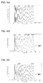
- 6A to 6C are diagrams for explaining an original sample pattern, a resolution by normal illumination of a comparative example, and super-resolution achieved by the microscope of the embodiment.
- FIG. 7A is a graph explaining the imaging electric field distribution when structural illumination or uniform intensity illumination is performed on the sample pattern shown in FIG.
- FIG. 6A, and FIG. 7B describes the spatial frequency components of the reproduced sample. It is a graph to do.
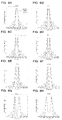
- 8A to 8H show the results of calculating the resolution of the microscope while changing the two-point interval of the sample under the first illumination condition.
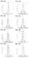
- 9A to 9H show the results of calculating the resolution of the microscope while changing the two-point interval of the sample under the second illumination condition.
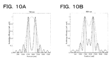
- 10A and 10B show the results of calculating the resolution of the microscope while changing the two-point interval of the sample under the second illumination condition.
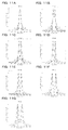
- 11A to 11G show the results of calculating the microscope resolution while changing the two-point interval of the sample under the third illumination condition.
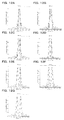
- 12A to 12G show the results of calculating the microscope resolution while changing the two-point interval of the sample under the fourth illumination condition.
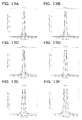
- 13A to 13F show the results of calculating the resolution of the microscope while changing the two-point interval of the sample under the fifth illumination condition.
- 14A to 14C are diagrams for explaining an original sample pattern, a resolution by normal illumination of a comparative example, and super-resolution achieved by the microscope of the embodiment.
- the microscope 100 is a structured illumination microscope, and includes a coherent light source 10, a structured illumination unit 20, a reference light irradiation unit 30, a basic light irradiation unit 40, an objective system 50, a light detection unit 60, and a control unit 90.
- the xy plane corresponding to the horizontal plane is parallel to the sample surface 88 a of the stage 88.
- the coherent light source 10 includes a laser device such as a semiconductor laser, and emits laser light L1 as coherent light. Although detailed description of the structure of the coherent light source 10 is omitted, the coherent light source 10 may be provided with an optical element such as a collimator.
- the structural illumination unit 20 includes a beam splitter 21, a movable mirror 22, a first oblique illumination mirror 24, a second oblique illumination mirror 25, a polarization beam splitter (PBS) 82, and a first shutter 28, and is coherent.
- Structural illumination lights L21 and L22 obtained by branching the structural illumination light L2 from the light source 10 are radiated from a pair of symmetrical oblique directions onto the sample surface 88a of the stage 88 at the sample position.
- the beam splitter 21 splits the light L2 from the polarization beam splitter 82 at a ratio of 1: 1.
- the movable mirror 22 is a plane mirror and reflects the light L22 from the beam splitter 21 to make it enter the second oblique illumination mirror 25.
- the first oblique illumination mirror 24 allows the light L21 to be incident on the sample surface 88a of the stage 88 or the surface OS to be inspected on the sample surface 88a, that is, the sample from a diagonally upper right direction at an inclination angle or an incident angle ⁇ . Illuminates the OS, etc.
- the second oblique illumination mirror 25 is a plane mirror, and allows the light L22 to be incident on the sample surface 88a or the surface (sample) OS to be inspected at an inclination angle or an incident angle ⁇ from an oblique upper left direction and the like. Illuminate.
- the oblique illumination lights L21 and L22 form structural illumination that is a standing wave.
- Lights L21 and L22 which are obliquely incident lights for forming structural illumination, are lights polarized in the y direction perpendicular to the paper surface, and the electric field is set parallel to the y direction.
- the movable mirror 22 is accompanied by a mirror driving unit 23 composed of a piezo element or the like, and a phase shift can be given to the light L22 by slightly moving the movable mirror 22 in the x direction, for example.
- the polarization beam splitter 82 cooperates with the ⁇ / 2 wavelength plate 81 to reflect the light L2 which is perpendicular to the paper surface and is polarized in the y direction to guide it to the beam splitter 21, and the light L12 which is polarized in the z direction parallel to the paper surface. Is transmitted and guided to the beam splitter 83.
- the rotation angle of the ⁇ / 2 wavelength plate 81 it is possible to adjust the relative intensity of the structural illumination light L2 that enters the structural illumination section 20.
- the reference light irradiation unit 30 includes a movable mirror 31, a beam expander 33, a lens 34, a mirror 35, a beam splitter 83, and a second shutter 38, and branches the reference light L3 from the coherent light source 10. Then, by irradiating the detection surface DS of the light detection unit 60, a uniform electric field shift, that is, a shift of the optical electric field is given to the image formation electric field distribution on the detection surface DS.
- the movable mirror 31 is a plane mirror, reflects the light L3 from the beam splitter 83, and makes it enter the mirror 35 via the beam expander 33 and the lens 34.
- the beam expander 33 expands the beam diameter of the reference light L3.
- the lens 34 cooperates with the lens 53 provided in the objective system 50 to collimate the reference light L3 and make the light L3 vertically incident on the detection surface DS of the light detection unit 60 as a plane wave.
- the movable mirror 31 is accompanied by a mirror drive unit 32 including a piezo element, and a phase shift can be given to the light L3 by slightly moving the movable mirror 31 in the x direction, for example.
- the beam splitter 83 partially transmits the light L12 which is parallel to the paper surface and is polarized in the z direction, and makes it enter the ⁇ / 2 wave plate 84 and the polarizing plate 85 as the reference light L3, and also the light having the same polarization.
- L4 is guided to the basic light irradiation unit 40.
- the rotation angle of the ⁇ / 2 wavelength plate 81 the relative intensity of the reference light L3 incident on the movable mirror 31 can be adjusted.
- the basic light irradiation unit 40 is an epi-illumination system including a beam expander 41, a ⁇ / 2 wavelength plate 42, a lens 43, a beam splitter 51, an objective lens 45, and a third shutter 48, and is a coherent light source.
- the light L4 for normal illumination is branched from 10 and is radiated through the objective lens 45 onto the sample surface 88a of the stage 88 at the sample position or the test surface OS.
- the beam expander 41 expands the beam diameter of the light L4 for normal illumination. By adjusting the rotation angle of the ⁇ / 2 wave plate 42, the polarization direction of the normal illumination light L4 incident on the objective lens 45 can be appropriately set.
- the lens 43 once collects the light L4 for normal illumination.
- the beam splitter 51 allows the light L4 for normal illumination that has passed through the lens 43 to pass through and makes it enter the objective lens 45.
- the light L4 emitted from the objective lens 45 and incident on the sample surface 88a of the stage 88 is collimated and vertically incident on the sample surface 88a as a plane wave. That is, the light L4 for normal illumination is used as epi-illumination.
- the objective system 50 includes an objective lens 45, a beam splitter 51, a polarizing plate 52, and a lens 53, and an image formed on the sample surface 88a of the stage 88 or the test surface OS is detected by the light detection unit 60. Project on the DS. Specifically, the scattering pattern of the scattered light LO1 by the test surface (sample) OS on the sample surface 88a illuminated by the illumination pattern of the structural illumination by the structural illumination unit 20 is transferred to the detection surface DS via the objective system 50. Projected.
- the scattered pattern of the scattered light LO1 by the surface to be inspected (sample) OS and the uniform plane wave for the reference light By making L3 interfere with the detection surface DS, it is possible to give a uniform electric field shift to the scattering pattern of the scattered light LO1 on the detection surface DS.
- the scattering pattern of the non-structural illumination type scattered light LO2 by the test surface (sample) OS on the sample surface 88a illuminated by the uniform illumination by the basic light irradiating unit 40 is detected through the objective system 50. Projected on.
- the light detection unit 60 is composed of a two-dimensional light sensor 61 such as a CCD sensor or a COMS sensor, and has a drive circuit 63 attached thereto.
- the stage 88 is supported on a drive unit 89 and can be two-dimensionally moved along the xy plane, and can be moved in the z direction to be aligned with the objective lens 45.
- FIG. 2 is a conceptual plan view of the sample surface 88a of the stage 88.
- the observation area AR of the sample surface 88a extends in the y direction by the structural illumination lights L21 and L22, and is periodically spaced in the x direction.
- An illumination pattern (structure illumination) IP having a stripe-shaped intensity pattern or a waveform arranged in a line is formed.
- control unit 90 centrally controls the operations of the coherent light source 10, the structural illumination unit 20, the reference light irradiation unit 30, the basic light irradiation unit 40, and the light detection unit 60.
- the control unit 90 is a computer and has an arithmetic processing unit 91.
- the arithmetic processing unit 91 can perform various kinds of digital signal processing on the image obtained by the light detection unit (imaging unit) 60, and particularly, the necessary determination processing, Fourier transform, and inverse Fourier transform are performed on the obtained signal. Various calculation processes including conversion can be performed, and super-resolution images are reconstructed.
- the control unit 90 can switch the illumination state by appropriately opening and closing the first to third shutters 28, 38 and 48.
- the first shutter 28 is opened and the second shutter 38 and the third shutter 48 are closed.
- the first shutter 28 and the second shutter 38 are opened, and the third shutter 48 is closed.
- uniform illumination is performed by the basic light irradiation unit 40
- the third shutter 48 is opened and the first shutter 28 and the second shutter 38 are closed.
- the control unit 90 estimates for the imaging electric field distribution under the structured illumination formed on the detection surface DS of the light detection unit 60, including positive and negative signs,
- the movable mirror 31 of the reference light irradiation unit 30 is shifted to give a phase shift to the reference light L3.
- the arithmetic processing unit 91 operates the structured illumination unit 20 and the reference light irradiation unit 30 to perform a Fourier transform on the pair of image formation electric field distributions detected by the photodetection unit 60, thereby performing uniform intensity illumination in the spatial frequency domain. Calculate a pair of electric field conversion functions that are spaced outside the spatial frequency band of the mold optical system.
- the arithmetic processing unit 91 operates the basic light irradiation unit 40 to perform Fourier transform on the image formation electric field distribution detected by the light detection unit 60 to calculate the electric field conversion function in the spatial frequency band of the conventional optical system. To do.
- the arithmetic processing unit 91 synthesizes a wideband Fourier transform signal in which an electric field transform function derived from structured illumination and an electric field transform function derived from uniform intensity illumination are combined, and an inverse Fourier transform is performed on the synthesized wideband Fourier transform signal. Is performed to reconstruct an image in which the spatial frequency band is expanded.
- the principle of super-resolution by the microscope 100 will be described.
- a coherent imaging system such as the microscope 100 of the embodiment
- the sample distribution is expressed as a coefficient for the (non-negative) illumination intensity.
- the sample distribution needs to be described as a coefficient for the illumination electric field (which can take a negative value) because of the coherence of the light waves emitted by the sample.
- the sample distribution scattering efficiency distribution, that is, the optical response coefficient to the illumination electric field
- the electric field distribution of the two-beam interference standing wave illumination by the coherent light source is I (x)
- the point spread function of the optical system is H ( x)
- the electric field distribution D (x) formed on the image plane by the scattered light from the sample is expressed by the following equation.
- I 0 , p, x, and ⁇ 0 represent the amplitude of the electric field, the spatial frequency of the structural illumination, the position, and the initial phase, respectively
- the operation symbol between represents convolution integral.
- An accurate description of the electric field distribution of the standing wave includes the time term, but the time term is omitted here to show that the phase of the electric field in the region belonging to the adjacent peaks of the standing wave differs by ⁇ at each time.
- the standing wave is expressed statically.
- Fourier transform (FX represents Fourier transform of X) is performed on both sides of the equation (1) to obtain the following equation.
- FS k + p
- FS k ⁇ p
- FS (k + p) and FS (k ⁇ p) as extended spatial frequency information
- FS (as basic spatial frequency information obtained based on the image forming electric field distribution (square root of image forming intensity distribution) by uniform intensity distribution illumination.
- the Fourier transform of the imaging electric field distribution is performed in the x direction and the y direction to obtain a pair of spatial frequency information expanded in the x direction.
- the band is expanded by the frequency p at least in the x direction. It is possible to obtain a dimensional super-resolution image.
- the scattered light from the sample on the sample surface 88a is an electric field distribution that can take positive and negative values as described above.
- an image pickup device such as a CCD sensor
- a time average (square of electric field) of an electric field that fluctuates at a high speed on a detection surface DS which is an image forming surface can be obtained, but the electric field itself cannot be obtained. Therefore, the electric field distribution on the detection surface DS is estimated by paying attention to the property that the scattered light due to the standing wave can have only two phases.
- phase of the scattered light by the sample depends on the phase of the illumination, focusing on the interference phenomenon of the scattered light, the phase of the scattered light on the detection surface DS is 0 (positive) or ⁇ (negative) corresponding to that of the standing wave. ) Can be considered to take any value of.
- a plane wave having the same wavelength as the scattered light (reference light shown as light L3 in FIG. 1) is made incident vertically on the detection surface DS and interferes with the scattered light to estimate the imaging electric field distribution on the detection surface DS.
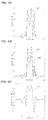
- FIG. 3A is a chart for explaining the light intensity distribution formed on the detection surface DS of the light detection unit 60 by the scattered light from the sample on the sample surface 88a which is structurally illuminated
- FIG. 3B is structurally illuminated
- 7 is a chart for explaining a light intensity distribution formed by causing reference light to interfere with a scattering pattern formed on the detection surface DS of the light detection unit 60 by scattered light from the sample on the sample surface 88a.
- the horizontal axis represents position and the vertical axis represents light intensity.
- 3C is an image formation electric field distribution of only the scattering pattern formed on the detection surface DS of the photodetection unit 60 by the scattered light from the sample on the sample surface 88a which is structurally illuminated, and includes positive and negative signs. Showing things.
- the horizontal axis is the same as in FIGS. 3A and 3B.
- the wavelength ⁇ of the laser beam L1 emitted from the coherent light source 10 is 488 nm
- the NA of the objective lens 45 is 0.4
- the incident angle ⁇ of the structural illumination is 45 degrees.
- the sample pattern on the sample surface 88a is a stripe pattern, and the interval is increased in increments of 50 nm from 100 nm intervals to 900 nm intervals (see FIG. 6A described later).
- the imaging electric field distribution (curve c1) as shown in FIG. 3C is measured by the two-dimensional optical sensor 61, the detected signal is squared by inverting the negative component as shown in FIG. 3A.
- the light intensity distribution (curve c2) is obtained. From such a light intensity distribution (curve c2), although the absolute value of the imaging electric field distribution (curve c1) as shown in FIG. 3C is obtained, the sign of the curve c1 cannot be determined. Therefore, the imaging electric field distribution (curve c1) of only the scattering pattern formed on the detection surface DS of the photodetecting section 60 by the scattered light from the sample on the sample surface 88a which is structurally illuminated has a predetermined uniform value.
- the curve c22 which is an image forming electric field distribution and is indicated by a broken line, is different from the reference light that gives a uniform electric field component having a phase different from that of the reference light in the curve c21 with respect to the curve c1 shown in FIG. 3C, that is, an initial phase state. It is a plane wave in a phase state, and more specifically, it is an imaging electric field distribution in which a plane wave having a phase shift of ⁇ / 2 with respect to the original is interfered.
- the curve c21 in the case of phase 0 is compared with the curve c21 in the case of phase 0, the peaks become higher and the peaks become lower. Can be classified by judging the positive / negative of the original peak before square.
- FIGS. 3A to 3C illustrate a case where the position of the structural illumination on the sample surface 88a is changed by the phase shift, and correspond to FIGS. 3A to 3C, respectively.
- a curve c21 indicated by a solid line interferes with the reference light that gives a predetermined uniform electric field component to the curve c1 shown in FIG. 4C, specifically, a plane wave in an initial phase state (that is, phase zero).
- a curved line c22 which is an image forming electric field distribution and is indicated by a broken line, is different from the reference light that gives a uniform electric field component having a phase different from that of the reference light on the curve c21 with respect to the curve c1 illustrated in FIG. 4C, that is, an initial phase state.
- a plane wave having a phase shift of ⁇ / 2 with respect to the original is interfered.
- the curve c21 in the case of phase ⁇ / 2 is compared with the curve c21 in the case of zero phase, there are a high peak portion and a low peak portion. Can be classified by judging the positive / negative of the original peak before square.
- the above method is not limited to the case where the positive electric field component added to the imaging electric field distribution (curve c1) is lower than the peak of the imaging electric field distribution (curve c1), but is added to the imaging electric field distribution (curve c1). This holds even when the positive electric field component is larger than the peak of the imaging electric field distribution (curve c1), and the imaging electric field distribution (curve c1) can be estimated including positive and negative signs.
- the sample is placed on the sample surface 88a of the stage 88 (step S11).
- the arithmetic processing unit 80 opens the first shutter 28 and closes the second shutter 38 and the third shutter 48 to perform the first structural illumination by the structural illumination unit 20 and measure the scattering pattern ( Step S12).
- the scattered light LO1 that does not include the reference light is incident on the detection surface DS, and the intensity distribution of the imaging pattern can be obtained on the detection surface DS for the sample affected by the structural illumination.
- step S13 only the state of the second shutter 38 is changed to the open state, and the structural illumination unit 20 and the reference light irradiation unit 30 perform the first measurement for checking the sign of the image formation electric field distribution (step S13).
- the scattering pattern of the scattered light LO1 by the test surface (sample) OS illuminated by the reference light irradiation unit 30 and the light L3 that is a uniform plane wave for reference interfere on the detection surface DS to cause interference.
- the intensity distribution of the pattern is obtained, a signal waveform having a peak pattern similar to that of the original scattered light LO1 is obtained with the phase of the light L3 as the initial phase state.
- the movable mirror 31 of the reference light irradiation unit 30 is operated to give an arbitrary phase shift ⁇ preset to the light L3 that is a uniform plane wave for reference, so that the phase of the scattered light LO1 changes.
- the second measurement is performed to obtain the intensity distribution of the interference pattern having the peak value changed by interfering with the above-described light L3 (step S14).
- Information for determining whether the sign of the imaging electric field distribution is positive or negative can be obtained by the first measurement and the second measurement described above, and the imaging including the positive and negative signs from the intensity distribution of the imaging pattern obtained in step S12. The electric field distribution can be calculated.
- the arithmetic processing unit 80 changes only the state of the second shutter 38 to the closed state, and also operates the movable mirror 22 of the structural illumination unit 20 to give a phase shift to the structural illumination light L21.
- the scattering pattern is measured (step S15).
- the phase shift amount is, for example, ⁇ / 2, but is not limited to this.
- the scattered light LO1 that does not include the reference light is incident on the detection surface DS, and the intensity distribution of the image formation pattern on the detection surface DS of the sample affected by the second structural illumination after the phase shift is calculated. Obtainable.
- the spatial formation of the light formed on the sample surface 88a can be improved. Shift the lighting pattern.
- the reference light irradiation unit 30 performs the third measurement for checking the sign of the image formation electric field distribution (step S16). At this time, the scattering pattern of the scattered light LO1 by the test surface (sample) OS illuminated by the reference light irradiation unit 30 and the light L3 that is a uniform plane wave for reference interfere on the detection surface DS to cause interference.
- a signal waveform having a peak pattern similar to that of the original scattered light LO1 is obtained with the phase of the light L3 as the initial phase state.
- the movable mirror 31 of the reference light irradiation unit 30 is operated to give an arbitrary phase shift ⁇ to the light L3 that is a uniform plane wave for reference, so that the scattered light LO1 and the light L3 whose phase is changed.
- the fourth measurement is performed to obtain the intensity distribution of the interference pattern having the peak value changed by interfering with each other (step S17).
- Information for determining whether the sign of the imaging electric field distribution is positive or negative can be obtained by the third measurement and the fourth measurement, and the imaging including the positive and negative signs from the intensity distribution of the imaging pattern obtained in step S15.
- the electric field distribution can be calculated. It should be noted that prior to the Fourier transform, which will be described later, how to give the sign (or definition of the sign) of the image formation electric field distribution by the first structured illumination obtained in step S14 and the image formation by the second structured illumination obtained in step S17.
- the position of the movable mirror 31 is returned to the original position before the operation of step S16, and the reference light in the third measurement of step S16 is performed.
- the phase state of is substantially matched with the phase state of the reference light in the first measurement in step S13. Further, the phase shift ⁇ in the fourth measurement in step S17 is made to substantially match the phase shift ⁇ in the second measurement in step S14.
- the arithmetic processing unit 80 opens the third shutter 48, closes the first shutter 28 and the second shutter 38, and performs uniform intensity illumination by the basic light irradiation unit 40 (step S18). At this time, the scattering pattern of the non-structural illumination type scattered light LO2 by the test surface (sample) OS illuminated by the basic light irradiation unit 40 is formed on the detection surface DS to obtain the intensity distribution of the imaging pattern. The intensity distribution of the scattered light LO2 is converted into the imaging electric field distribution.
- the image forming electric field distribution can be processed as positive or negative uniform. Further, regarding the image formation electric field distribution of the uniform intensity illumination, the consistency or continuity of the waveform in the boundary region where the signal components of the spatial frequency overlap after the Fourier transform described later is determined, and in steps S14 and S17. It is possible to secure the consistency of the positive and negative signs with respect to the imaged electric field distribution under the obtained structured illumination.
- the positive and negative signs can be determined by using the reference light as in the structural illumination, and the image forming electric field distribution including the sign can be calculated. it can.
- the arithmetic processing unit 91 performs a Fourier transform on the image forming electric field distribution acquired in step S14 and the image forming electric field distribution acquired in step S17, and also performs a Fourier transform on the image forming electric field distribution acquired in step S18. Is performed (step S19).
- Fourier transforms FS (k + p) and FS (k ⁇ p) of the optical response distribution of the sample can be obtained on the sample surface 88a, and the Fourier transform or the like is performed on the imaging electric field distribution acquired in step S18. Then, the electric field conversion function FS (k) is directly obtained.
- the arithmetic processing unit 91 combines the functions FS (k + p), FS (k ⁇ p), and FS (k) obtained in step S19 within the spatial frequency and makes them uniform with the imaging electric field distribution derived from structural illumination.
- a broadband Fourier transform signal obtained by connecting the image formation electric field distribution by the intensity illumination is acquired (step S20).
- averaging or truncation processing is performed in the boundary area of spatial frequencies.
- the arithmetic processing unit 91 performs an inverse Fourier transform on the synthesized wide band Fourier transform signal to obtain an absolute value and reconstructs a high resolution image in which the spatial frequency band is expanded (step S21).
- the reference light irradiator 30 branches the reference light L3 from the coherent light source 10 and irradiates the detection surface DS of the light detector 60 with a uniform electric field shift. Therefore, it is possible to acquire the spatial frequency information corresponding to the imaging electric field distribution under structured illumination, and thus the signal of the optical response distribution, and even if the coherent imaging system using coherent light is used, the resolution is high while the resolution is high.
- the target image can be acquired with reliability.
- FIG. 6A is a diagram showing a specific example of the original sample pattern.
- FIG. 6B is a diagram illustrating a result of resolution achieved when the microscope 100 does not use structured illumination
- FIG. 6C illustrates a result of super-resolution achieved by using structured illumination in the microscope 100 according to the embodiment. It is a figure explaining a result.
- the horizontal axis shows the position, and the vertical axis shows the scattering efficiency.
- the vertical axis represents the scattering efficiency as the degree of easiness of scattering as an index indicating the presence of the sample, but for the curve of the observed image under uniform intensity illumination, the image intensity distribution is plotted instead. .
- the original sample pattern (dashed lines in FIGS. 6B and 6C) has increased spacing in increments of 50 nm from 100 nm spacing to 900 nm spacing.
- FIG. 7A is a graph for explaining the imaging electric field distribution when structural illumination or uniform intensity illumination is performed on the sample pattern shown in FIG. 6A.
- the horizontal axis shows the position, and the vertical axis shows the value of the electric field.
- the wavelength ⁇ of the laser light L1 emitted from the coherent light source 10 is 488 nm
- the incident angle ⁇ is 45 degrees
- the NA of the objective lens 45 is 0.4.
- the solid and broken lines correspond to the images acquired under the first and second structured illuminations with different phases
- the dotted or thin lines correspond to the images captured with uniform intensity illumination.
- FIG. 7B is a graph illustrating the spatial frequency components of the reproduced sample.
- the solid line with the peak in the center is the spatial frequency component obtained by uniform intensity illumination
- the broken line with the peaks on the left and right is the spatial frequency component obtained using structural illumination
- the sample represented by the dotted line originally has It can be seen that the frequency components that are present are almost restored.
- the maximum spatial frequency that can be acquired by a microscope is NA / ⁇ , where ⁇ is the wavelength for general uniform intensity illumination.
- the minimum spatial frequency achieved by the microscope 100 of the embodiment is NA / ⁇ + sin ⁇ / ⁇ .
- the resolvable interval is 1220 nm in general uniform intensity illumination
- the resolvable interval is 440 nm in the microscope 100 of the embodiment. Means that. An image reconstructed by general uniform intensity illumination (see the solid line in FIG. 6B) and an image reconstructed from the imaging electric field distribution using the structured illumination of the embodiment (see the solid line in FIG. 6C) are compared. Then, it is understood that the structured illumination according to the embodiment can resolve up to a sample interval of about 450 nm. On the other hand, with general uniform intensity illumination, it can be seen that resolution is not easy even at intervals of 900 nm.
- the following describes the resolution (two-point resolution) related to the observation of a sample consisting of two points that are close to each other.
- FIG. 8A shows a case where the two-point spacing of the sample is 300 nm
- FIG. 8B shows a case where the two-point spacing of the sample is 320 nm
- FIG. 8C shows a case where the two-point spacing of the sample is 350 nm. Shows a case where the two-point spacing of the sample is 400 nm
- FIG. 8E shows a case where the two-point spacing of the sample is 450 nm
- FIG. 8F shows a case where the two-point spacing of the sample is 500 nm
- FIG. FIG. 8H shows the case where the two-point spacing of the sample is 800 nm
- FIG. 8H shows the case where the two-point spacing of the sample is 900 nm.
- FIGS. 10A and 10B are resolutions when the wavelength ⁇ of the laser light L1 emitted from the coherent light source 10 is 488 nm, the incident angle ⁇ is 60 degrees, and the NA of the objective lens 45 is 0.5.
- the results are shown.
- 9A shows a case where the two-point spacing of the sample is 200 nm
- FIG. 9B shows a case where the two-point spacing of the sample is 250 nm
- FIG. 9C shows a case where the two-point spacing of the sample is 300 nm
- FIG. 9E shows a case where the two-point spacing of the sample is 350 nm
- FIG. 9F shows a case where the two-point spacing of the sample is 400 nm
- FIG. The case where the two-point interval of the sample is 500 nm is shown
- FIG. 9H shows the case where the two-point interval of the sample is 600 nm
- FIG. 10A shows the case where the two-point spacing of the sample is 700 nm
- FIG. 10B shows the case where the two-point spacing of the sample is 800 nm.
- a broken line indicates a two-point peak of the sample
- a solid line indicates a resolution using the structural illumination of the embodiment
- a dotted line or a thin line indicates a resolution using general uniform intensity illumination. Show.
- a sufficient resolution is achieved by the reconstruction of two points at 300 nm intervals shown in FIG. 9C, but in the uniform intensity illumination of the comparative example, two points at 700 nm intervals shown in FIG. 10A are obtained. It can be seen that even about is not sufficiently separated. Note that, assuming the wavelength ⁇ , the incident angle ⁇ , and NA, the theoretically resolvable interval is 976 nm in uniform intensity illumination, and the theoretically resolvable interval is 976 nm in the microscope 100 of the embodiment. Is 357 nm, so the resolution result shown in the figure matches the theoretical resolution.
- 11A to 11G show the resolution results when the wavelength ⁇ of the laser light L1 emitted from the coherent light source 10 is 488 nm, the incident angle ⁇ is 80 degrees, and the NA of the objective lens 45 is 0.6.
- 11A shows the case where the two-point spacing of the sample is 200 nm
- FIG. 11B shows the case where the two-point spacing of the sample is 250 nm
- FIG. 11C shows the case where the two-point spacing of the sample is 300 nm. Shows a case where the two-point spacing of the sample is 400 nm
- FIG. 11E shows a case where the two-point spacing of the sample is 500 nm
- FIG. 11F shows a case where the two-point spacing of the sample is 600 nm, and FIG. The case where the two-point interval of the sample is 700 nm is shown.
- a broken line indicates a two-point peak of the sample
- a solid line indicates a resolution using the structural illumination of the embodiment
- a dotted line or a thin line indicates a resolution using general uniform intensity illumination. Show.
- a sufficient resolution is achieved by the reconstruction of two points at 250 nm intervals shown in FIG. 11B, but in the uniform intensity illumination of the comparative example, two points at 600 nm intervals shown in FIG. 11F are obtained. It can be seen that even about is not sufficiently separated.
- the theoretically resolvable interval is 813 nm in uniform intensity illumination, and the theoretically resolvable interval is 813 nm in the microscope 100 of the embodiment. Is 307 nm, the resolution result shown above matches the theoretical resolution.
- FIG. 12A to 12G show the resolution results when the wavelength ⁇ of the laser light L1 emitted from the coherent light source 10 is 488 nm, the incident angle ⁇ is 80 degrees, and the NA of the objective lens 45 is 0.7.
- . 12A shows a case where the two-point spacing of the sample is 200 nm
- FIG. 12B shows a case where the two-point spacing of the sample is 250 nm
- FIG. 12C shows a case where the two-point spacing of the sample is 300 nm
- FIG. 12E shows a case where the two-point spacing of the sample is 500 nm
- FIG. 12F shows a case where the two-point spacing of the sample is 550 nm, and FIG. The case where the two-point interval of the sample is 600 nm is shown.
- a broken line indicates a two-point peak of the sample
- a solid line indicates a resolution using the structural illumination of the embodiment
- a dotted line or a thin line indicates a resolution using general uniform intensity illumination. Show.
- a sufficient resolution is achieved by the reconstruction of two points at 250 nm intervals shown in FIG. 12B, but in the uniform intensity illumination of the comparative example, two points at 550 nm intervals shown in FIG. 12F are obtained. It can be seen that even about is not sufficiently separated.
- the theoretically resolvable interval is 697 nm in uniform intensity illumination, and the theoretically resolvable interval is 697 nm in the embodiment of the microscope 100. Is 289 nm, so the resolution result shown in the figure matches the theoretical resolution.
- 13A to 13F show resolution results when the wavelength ⁇ of the laser light L1 emitted from the coherent light source 10 is 488 nm, the incident angle ⁇ is 80 degrees, and the NA of the objective lens 45 is 0.95.
- . 13A shows a case where the two-point spacing of the sample is 150 nm
- FIG. 13B shows a case where the two-point spacing of the sample is 180 nm
- FIG. 13C shows a case where the two-point spacing of the sample is 200 nm
- FIG. 13E shows the case where the 2-point spacing of the sample is 350 nm
- FIG. 13F shows the case where the 2-point spacing of the sample is 400 nm.
- a broken line indicates a two-point peak of the sample
- a solid line indicates a resolution using the structural illumination of the embodiment
- a dotted line or a thin line indicates a resolution using general uniform intensity illumination. Show.
- a sufficient resolution is achieved by the reconstruction of two points at 200 nm intervals shown in FIG. 13C, but in the uniform intensity illumination of the comparative example, two points at 350 nm intervals shown in FIG. 13E are obtained. It can be seen that even for, the separation is not very clear.
- the theoretically resolvable interval is 426 nm in the uniform intensity illumination, and the theoretically resolvable interval is 426 nm in the microscope 100 of the embodiment. Is 209 nm, so the resolution result shown in the figure matches the theoretical resolution.
- FIGS. 6A to 6C are diagrams for explaining the two-dimensional simulation results corresponding to FIGS. 6A to 6C.
- FIG. 14A is a diagram showing a specific example of the original sample pattern corresponding to FIG. 6A, and the original sample pattern is a stripe pattern in which the interval in the x direction is gradually increased.
- FIG. 14B is a diagram illustrating a result of two-dimensional resolution achieved when the microscope 100 does not use structured illumination
- FIG. 14C illustrates two-dimensional resolution achieved by using structured illumination in the microscope 100 of the embodiment. It is a figure explaining the result of resolution.
- the wavelength ⁇ of the laser light L1 emitted from the coherent light source 10 is 488 nm
- the incident angle ⁇ is 45 degrees
- the NA of the objective lens 45 is 0.4.
- the periodic direction of the illumination pattern (structural illumination) IP is not limited to the x direction, and can be any direction, and structural illumination can be performed with the periodic direction set to any arbitrary direction. Can improve the resolution in an arbitrary direction (not limited to a single direction).
- structural illumination as in the embodiment is performed not only in the x direction but also in the y direction, and a pair of spatial frequency information in each direction is obtained from the Fourier transform of the imaging electric field distribution for the structural illumination in each direction. .
- the resolution is improved in the x direction and the y direction.
- a super-resolution image can be obtained.
- the signal component of the super-resolution spatial frequency calculated from the imaging electric field distribution obtained under a single type of structured illumination is the normal solution corresponding to the imaging electric field distribution obtained under uniform intensity illumination.
- the spatial frequency information or spatial frequency distribution without local discontinuity is obtained by partially overlapping with the signal component of the spatial frequency of the image, but the imaging electric field distribution obtained under multiple types of structural illumination is obtained. It can also be combined. That is, the signal components of the spatial frequency of two steps of super-resolution calculated from the image formation electric field distribution obtained under the structural illumination with different spatial frequencies are connected together, and the image formation electric field distribution obtained under the uniform intensity illumination is obtained. By further connecting the signal components of the corresponding spatial frequencies of normal resolution, it is possible to obtain spatial frequency information without interruption over a wide range.
- the basic light irradiation unit 40 is incorporated in the microscope 100, but the basic light irradiation unit 40 is not essential and can be omitted.
- the lights L21 and L22 for structural illumination are arranged symmetrically as long as they are incident from opposite sides with the objective lens 45 interposed therebetween or are incident from opposite sides with the optical axis of the objective lens 45 interposed therebetween. It doesn't have to be a dish. That is, the incident angles ⁇ of the structural illumination lights L21 and L22 may not be equal, but it is desirable that the intensities of the lights L21 and L22 be equal from the viewpoint of increasing the reliability of resolution.
- structural illumination can be achieved not only by shifting the relative phases of the obliquely incident lights L21 and L22, but also by shifting the stage 88 itself, which should be the sample surface 88a, in the x direction in which the strong and weak patterns are repeated. Is.
- the imaging electric field distribution is estimated from the increase / decrease in the light intensity detected by the photodetection unit 60 corresponding to the electric field shift due to the reference light L3, including positive and negative signs (FIGS. 3A to 3C). It is also possible to estimate the imaging electric field distribution including positive and negative signs from the degree of increase / decrease in the light intensity detected by the photodetector 60 corresponding to the electric field shift.
Landscapes
- Physics & Mathematics (AREA)
- Analytical Chemistry (AREA)
- General Physics & Mathematics (AREA)
- Chemical & Material Sciences (AREA)
- General Health & Medical Sciences (AREA)
- Biochemistry (AREA)
- Life Sciences & Earth Sciences (AREA)
- Health & Medical Sciences (AREA)
- Immunology (AREA)
- Pathology (AREA)
- Optics & Photonics (AREA)
- Engineering & Computer Science (AREA)
- Multimedia (AREA)
- Microscoopes, Condenser (AREA)
- Investigating Or Analysing Materials By Optical Means (AREA)
Abstract
コヒーレント結像によって高解像ながら高い信頼性で対象像を取得することができる顕微鏡及び顕微法を提供する。顕微鏡100は、コヒーレント光源10と、コヒーレント光源10から構造照明用の光L21,L22を分岐して略対称的な一対の斜め方向から試料面88aの試料位置に照射する構造照明部20と、試料面88aの試料位置から射出された散乱光LO1の分布を対物レンズ45を介して検出する光検出部60と、コヒーレント光源10から参照用の光L3を分岐して光検出部60の検出面DSに照射することによって一様な電場シフトを与える参照光照射部30とを備える。
Description
本発明は、構造照明型の顕微鏡及び顕微法に関し、特にコヒーレント結像によって対象像を取得する顕微鏡及び顕微法に関する。
構造照明顕微法(Structured Illumination Microscopy, SIM)は、回折限界を超える光学的超解像顕微法の一つである。これまで光学的超解像法は、主にインコヒーレント結像系で蛍光観察を行うバイオ分野で開発が進められてきた。一方で、光学的計測にはコヒーレント結像系を前提とする用途が存在し、半導体デバイスの欠陥検査はその一例である。
しかしながら、一般的な2光波干渉による定在波を構造照明に用いるとコヒーレント系に特有の干渉が起き、結像が照明の強度分布に線形でなくなるため、強度分布取得では不十分で、電場分布を取得する必要性が生じてくる。一般に撮像素子では、電場分布を直接取得できずその時間平均(強度分布)しか取得できない。この問題を解決するため、3光波の干渉による定在波を構造照明として使うことで、結像を照明の強度分布に線形にするという手法が提案されている(特許文献1参照)。ただし、この手法では、バイアス用振幅で振動するバイアス平面波を精密に形成する必要がある。
本発明は、上記背景技術に鑑みてなされたものであり、コヒーレント結像によって高解像ながら高い信頼性で対象像を取得することができる顕微鏡及び顕微法を提供することを目的とする。
上記目的を達成するため、本発明に係る顕微鏡は、コヒーレント光源と、コヒーレント光源から構造照明用の光を分岐して略対称的な一対の斜め方向から試料位置に照射する構造照明部と、試料位置から射出された散乱光の分布を対物レンズを介して検出する光検出部と、コヒーレント光源から参照用の光を分岐して光検出部の検出面に照射することによって一様な電場シフトを与える参照光照射部とを備える。
上記顕微鏡では、参照光照射部がコヒーレント光源から参照用の光を分岐して光検出部の検出面に照射することによって一様な電場シフトを与えるので、構造照明下での結像電場分布に対応する空間周波数情報延いては光学応答分布の信号を取得することができ、コヒーレント光を用いるコヒーレント結像系であっても、高解像ながら高い信頼性で対象像を取得することができる。
本発明の具体的な側面によれば、上記顕微鏡において、参照光照射部は、構造照明部によって照明された試料位置から射出され光検出部の検出面に形成された散乱パターンに位相の異なる参照用の光を干渉させる。この場合、結像電場分布に対して直接的に一様な電場シフトを与えることができる。
本発明の別の側面によれば、参照光照射部は、光検出部の検出面上の散乱パターンに重ねて初期位相状態の平面波と、初期位相状態とは異なる位相状態の平面波とを順次照射する。
本発明のさらに別の側面によれば、一様な電場シフトに対応して光検出部によって検出される光強度の増減から結像電場分布を正負の符号を含めて見積もる。この場合、結像電場分布に相当する信号を符号を含めて取得することができ、結像電場分布の信号に対してフーリエ変換を行うことができる。
本発明のさらに別の側面によれば、構造照明部は、試料位置に形成される光の空間的な照明パターンとしての構造照明をシフトさせる。この場合、一対の構造照明を試料位置に形成することができ、構造照明により周波数シフトした試料信号成分を算術的に分離でき、超解像情報を抽出することができる。
本発明のさらに別の側面によれば、構造照明部は、一対の斜め方向から照射する光の位相を相対的にシフトさせる。この場合、構造照明の位相をシフトさせた一対の結像電場分布に相当する信号を取得することができる。
本発明のさらに別の側面によれば、構造照明部は、試料位置に一対の平面波を照射することによって構造照明を形成する。
本発明のさらに別の側面によれば、一対の斜め方向から照射する光は、強度が等しい。
本発明のさらに別の側面によれば、コヒーレント光源から通常照明用の光を分岐して対物レンズ越しに試料位置に照射する基本光照射部をさらに備える。この場合、一様照明に対応する低周波数成分に対応する光学応答分布を含めた対象像の再生が可能になる。
本発明のさらに別の側面によれば、基本光照射部は、構造照明部による構造照明がない状態で試料位置に平面波を照射する。この場合、一様強度分布の照明による光学応答分布を得ることができる。
本発明のさらに別の側面によれば、構造照明部及び参照光照射部を動作させて光検出部によって検出した結像電場分布と、基本光照射部を動作させて光検出部によって検出した結像電場分布とに基いて、構造照明の空間周波数に対応させて空間周波数帯域を拡張した画像を再構成する演算処理部をさらに備える。この場合、構造照明を利用した高解像成分を含む対象画像を得ることができる。
上記目的を達成するため、本発明に係る顕微法は、コヒーレント光源からの光を分岐して略対称的な一対の斜め方向から試料位置に照射する構造照明部と、試料位置から射出された散乱光の分布を対物レンズを介して検出する光検出部と、コヒーレント光源から参照用の光を分岐して光検出部の検出面に照射する参照光照射部と、を備える顕微鏡を用いた顕微法であって、試料位置において一対の構造照明を照射して散乱光を取り出すとともに、光検出部の検出面で参照用の光を干渉させることによって一様な電場シフトを与え、結像電場分布に相当する信号を取得する工程と、一対の構造照明下で得た結像電場分布に相当する信号のフーリエ変換から拡張空間周波数情報を抽出し逆フーリエ変換することによって、試料像を再構成する。
上記顕微法では、試料位置において一対の構造照明を照射して散乱光を取り出すとともに光検出部の検出面で参照用の光を干渉させることによって一様な電場シフトを与えるので、構造照明下で結像電場分布に対応する空間周波数情報延いては光学応答分布の信号を取得することができ、コヒーレント光を用いるコヒーレント結像系であっても、高解像ながら高い信頼性で対象像を取得することができる。
本発明の具体的な側面によれば、上記顕微法において、顕微鏡がコヒーレント光源から通常照明用の光を分岐して対物レンズ越しに試料位置に照射する基本光照射部をさらに備え、拡張空間周波数情報と、通常照明下で検出した信号のフーリエ変換から得た基本空間周波数情報とを合成し、逆フーリエ変換することによって、試料像を再構成する。
以下、図1等を参照して、本発明に係る一実施形態の顕微鏡について説明する。本顕微鏡100は、構造照明顕微鏡であり、コヒーレント光源10と、構造照明部20と、参照光照射部30と、基本光照射部40と、対物系50と、光検出部60と、制御部90とを備える。図示の顕微鏡100において、水平平面に対応するxy面は、ステージ88の試料面88aに平行になっている。
コヒーレント光源10は、半導体レーザその他のレーザ装置を備え、コヒーレント光としてのレーザ光L1を射出する。コヒーレント光源10は、詳細な構造の説明を省略するが、例えばコリメータ等の光学要素を付随させたものとすることができる。
構造照明部20は、ビームスプリッタ21と、可動ミラー22と、第1斜照明ミラー24と、第2斜照明ミラー25と、偏光ビームスプリッタ(PBS)82と、第1シャッター28とを備え、コヒーレント光源10から構造照明用の光L2を分岐することによって得た構造照明光L21,L22を、対称的な一対の斜め方向から試料位置であるステージ88の試料面88a上に照射する。ビームスプリッタ21は、偏光ビームスプリッタ82からの光L2を1:1の比で分岐する。可動ミラー22は、平面ミラーであり、ビームスプリッタ21からの光L22を反射して第2斜照明ミラー25に入射させる。第1斜照明ミラー24は、ステージ88の試料面88a又は試料面88a上の被検面OSつまりサンプルに対して傾斜角又は入射角θで斜め右上方向から光L21を入射させることで被検面OS等を照明する。第2斜照明ミラー25は、平面ミラーであり、試料面88a又は被検面(サンプル)OSに対して傾斜角又は入射角θで斜め左上方向から光L22を入射させることで被検面OS等を照明する。斜入射光である光L21,L22によって定在波である構造照明が形成される。構造照明を形成するための斜入射光である光L21,L22は、紙面に垂直なy方向に偏光した光であり、電場がy方向に平行に設定されている。可動ミラー22には、ピエゾ素子等からなるミラー駆動部23が付随しており、可動ミラー22を例えばx方向に微小移動させることで光L22に対して位相シフトを与えることができる。
偏光ビームスプリッタ82は、λ/2波長板81と協働して紙面に垂直でy方向に偏光した光L2を反射してビームスプリッタ21に導くとともに、紙面に平行なz方向に偏光した光L12を透過させてビームスプリッタ83に導く。ここで、λ/2波長板81の回転角の調整により、構造照明部20に入射させる構造照明用の光L2の相対的な強度を調整することができる。
参照光照射部30は、可動ミラー31と、ビームエキスパンダ33と、レンズ34と、ミラー35と、ビームスプリッタ83と、第2シャッター38とを備え、コヒーレント光源10から参照用の光L3を分岐して光検出部60の検出面DSに照射することによって検出面DS上の結像電場分布に対して一様な電場のシフトつまり光電界のシフトを与える。可動ミラー31は、平面ミラーであり、ビームスプリッタ83からの光L3を反射し、ビームエキスパンダ33及びレンズ34を介してミラー35に入射させる。ここで、ビームエキスパンダ33は、参照用の光L3のビーム径を拡大する。レンズ34は、対物系50に設けたレンズ53と協働して、参照用の光L3をコリメートして光検出部60の検出面DS上に平面波として垂直入射させる。可動ミラー31には、ピエゾ素子等からなるミラー駆動部32が付随しており、可動ミラー31を例えばx方向に微小移動させることで光L3に対して位相シフトを与えることができる。
ビームスプリッタ83は、紙面に平行でz方向に偏光した光L12を部分的に透過させ、参照用の光L3としてλ/2波長板84及び偏光板85に入射させるとともに、同様の偏光である光L4を基本光照射部40に導く。ここで、λ/2波長板81の回転角の調整により、可動ミラー31に入射させる参照用の光L3の相対的な強度を調整することができる。
基本光照射部40は、ビームエキスパンダ41と、λ/2波長板42と、レンズ43と、ビームスプリッタ51と、対物レンズ45と、第3シャッター48とを備える落射照明系であり、コヒーレント光源10から通常照明用の光L4を分岐して対物レンズ45越しに試料位置であるステージ88の試料面88a又は被検面OSに照射する。ビームエキスパンダ41は、通常照明用の光L4のビーム径を拡大する。λ/2波長板42は、その回転角の調整により、対物レンズ45に入射させる通常照明用の光L4の偏光方向を適宜設定することができる。レンズ43は、通常照明用の光L4を一旦集光する。ビームスプリッタ51は、レンズ43を経た通常照明用の光L4を透過させることによって対物レンズ45に入射させる。対物レンズ45から射出されステージ88の試料面88aに入射する光L4は、コリメートされ、試料面88a上に平面波として垂直入射する。つまり、通常照明用の光L4は落射照明として用いられる。
対物系50は、対物レンズ45と、ビームスプリッタ51と、偏光板52と、レンズ53とを備え、ステージ88の試料面88a又は被検面OSに形成された像を光検出部60の検出面DS上に投影する。具体的には、構造照明部20による構造照明の照明パターンによって照明された試料面88a上の被検面(サンプル)OSによる散乱光LO1の散乱パターンが、対物系50を介して検出面DSに投影される。この散乱光LO1に対して参照光照射部30によって参照用の光L3を照射することで、被検面(サンプル)OSによる散乱光LO1の散乱パターンと、参照用の一様な平面波である光L3とを検出面DS上で干渉させ、検出面DS上の散乱光LO1の散乱パターンに対して一様な電場シフトを与えることができる。また、基本光照射部40による一様照明によって照明された試料面88a上の被検面(サンプル)OSによる非構造照明型の散乱光LO2の散乱パターンが、対物系50を介して検出面DSに投影される。
光検出部60は、CCDセンサ、COMSセンサ等の2次元光センサ61で構成され、駆動回路63を付随させたものとなっている。
ステージ88は、駆動部89上に支持されており、xy面に沿って2次元的に移動可能であり、z方向に移動して対物レンズ45に対する位置合わせが可能になっている。
図2は、ステージ88の試料面88aの概念的な平面図であり、試料面88aの観察領域ARには、構造照明用の光L21,L22によってy方向に延びx方向に等間隔で周期的に配列されたストライプ状の強弱パターン又は波形である照明パターン(構造照明)IPが形成されている。
図1に戻って、制御部90は、コヒーレント光源10、構造照明部20、参照光照射部30、基本光照射部40、及び光検出部60の動作を統括的に制御している。制御部90は、コンピューターであり、演算処理部91を有している。演算処理部91は、光検出部(撮像部)60によって得た画像に対して各種のデジタル信号処理を行うことができ、特に得られた信号に対して必要な判定処理、フーリエ変換、逆フーリエ変換等を含む各種演算処理を行うことができ、超解像画像の再構築を行う。具体的には、制御部90は、第1~第3シャッター28,38,48を適宜開閉動作させることにより照明状態を切り換えることができる。構造照明部20によって構造照明を行う場合、第1シャッター28を開状態にし、かつ、第2シャッター38及び第3シャッター48を閉状態にする。構造照明によって得た強度分布から符号を含めた結像電場分布を得る際には、第1シャッター28及び第2シャッター38を開状態にし、かつ、第3シャッター48を閉状態にする。また、基本光照射部40によって一様照明を行う場合、第3シャッター48を開状態にし、第1シャッター28及び第2シャッター38を閉状態にする。構造照明部20によって構造照明を行う場合、制御部90は、照明パターンIPに位相シフトを与える目的で、構造照明部20の可動ミラー22をシフトさせて構造照明用の光L21に位相シフトを与える。さらに、構造照明部20によって構造照明を行う場合、制御部90は、光検出部60の検出面DS上に形成される構造照明下の結像電場分布について正負の符号を含めて見積もる目的で、参照光照射部30の可動ミラー31をシフトさせて参照用の光L3に位相シフトを与える。演算処理部91は、構造照明部20及び参照光照射部30を動作させて光検出部60によって検出した一対の結像電場分布に対してフーリエ変換を行って、空間周波数領域において一様強度照明型の光学系の空間周波数帯域の外側に離間した一対の電場変換関数を算出する。さらに、演算処理部91は、基本光照射部40を動作させて光検出部60によって検出した結像電場分布に対してフーリエ変換を行って従来的光学系の空間周波数帯域で電場変換関数を算出する。演算処理部91は、構造照明由来の電場変換関数と一様強度照明による電場変換関数とを繋ぎ合わせた広帯域のフーリエ変換信号を合成し、合成された広帯域のフーリエ変換信号に対して逆フーリエ変換を行って空間周波数帯域を拡張した画像を再構成する。
ここで、顕微鏡100による超解像の原理について説明する。実施形態の顕微鏡100のようなコヒーレント結像系では、結像過程で光波の電場レベルの干渉が起こるため、取得される結像強度分布から電場分布を推定することが必要である。インコヒーレント結像系におけるSIMでは、試料の光学応答が構造照明の光強度(電場の時間平均)に対して線形であると仮定するため、試料分布は(非負である)照明強度に対する係数として表現される。しかしコヒーレント結像系では、試料の発する光波の可干渉性のため、試料分布は(負値を取り得る)照明電場に対する係数として記述する必要がある。試料分布(散乱効率分布、すなわち照明電場に対する光学応答係数)をS(x)、コヒーレント光源による2光束干渉定在波照明の電場分布をI(x)、光学系の点像分布関数をH(x)とすると、試料からの散乱光が結像面に形成する電場分布D(x)は次式で表される。
 ここでI0,p,x,φ0は、それぞれ電場の振幅、構造照明の空間周波数、位置、及び初期位相を表し、{I(x)・S(x)}とH(x)との間の演算記号は畳み込み積分を表す。定在波の電場分布の正確な記述は時間項を含むが、定在波の隣り合うピークに属する領域の電場の位相が各時刻でπだけ異なることを表すために、ここでは時間項を省略し定在波を静的に表現する。式(1)の両辺をフーリエ変換(FXはXのフーリエ変換を表す)して次式を得る。
 ここで、構造照明の位相をφ1だけシフトさせた画像を取得し式(2)を連立することで、2つの未知数FS(k+p)及びFS(k-p)について解くことができる。拡張空間周波数情報としてのFS(k+p)及びFS(k-p)と、一様強度分布照明による結像電場分布(結像強度分布の平方根)に基いて得られる基本空間周波数情報としてのFS(k)とを周波数空間内で結合することにより、周波数pだけ帯域が拡大された超解像画像を得ることができる。
以上では、説明を簡単にするため、1次元的な試料パターン、つまり1次元的な光学応答パターンを有するサンプルを前提として説明を行ったが、2次元的な光学応答パターンを有するサンプルについても同様の処理が可能である。ただしこの場合、x方向及びy方向に関して結像電場分布のフーリエ変換を行って、x方向に拡張した一対の空間周波数情報を得る。さらに、x方向に拡張した一対の空間周波数情報と、一様強度分布照明による結像電場分布から得た空間周波数情報とを結合することにより、少なくともx方向に関して周波数pだけ帯域が拡大された2次元的な超解像画像を得ることができる。以上のような2次元のフーリエ変換処理については、公知の手法(例えば、Lal, Amit, Chunyan Shan, and Peng Xi. "Structured illumination microscopy image reconstruction algorithm." IEEE Journal of Selected Topics in Quantum Electronics 22.4 (2016): 50-63.)を用いることができる。
コヒーレント結像系において試料の光学応答係数等を扱う場合、上記のように試料面88a上の試料からの散乱光を、正負の値を取り得る電場分布として取り扱う必要がある。一般にCCDセンサ等の撮像素子による計測では、結像面である検出面DSで高速で変動する電場の時間平均(電場の自乗)が得られるが、電場そのものを得ることはできない。そこで、定在波による散乱光が2通りの位相しか取り得ないという性質に着目して検出面DSにおける電場分布を推定する。試料による散乱光の位相は照明の位相に依存するため、散乱光の干渉現象に着目すると、検出面DSにおける散乱光の位相は、定在波のそれに対応して0(正)またはπ(負)のいずれかの値をとるとみなすことができる。そこで、散乱光と同じ波長を持つ平面波(図1に光L3として示す参照光)を検出面DSに垂直に入射させ散乱光と干渉させることで、検出面DSにおける結像電場分布を推定することができる。散乱光の位相は2通りしかないため、上記参照光の位相を1回シフトさせ結像強度分布の増減をみることで結像面である検出面DS内の任意の位置の電場が推定可能になる。
図3Aは、構造照明されている試料面88a上のサンプルからの散乱光によって光検出部60の検出面DS上に形成される光強度分布を説明するチャートであり、図3Bは、構造照明されている試料面88a上のサンプルからの散乱光によって光検出部60の検出面DS上に形成される散乱パターンに対して参照光を干渉させて形成される光強度分布を説明するチャートである。図3A及び3Bにおいて、横軸は位置を示し、縦軸は光強度を示す。図3Cは、構造照明されている試料面88a上のサンプルからの散乱光によって光検出部60の検出面DS上に形成される散乱パターンのみの結像電場分布であって、正負の符号を含むものを示している。図3Cにおいて、横軸は図3A及び3Bと同様となっている。以上の具体例において、コヒーレント光源10から射出させるレーザ光L1の波長λを488nmとし、対物レンズ45のNAを0.4とし、構造照明の入射角度θを45度としている。試料面88a上のサンプルパターンは、ストライプパターンであって、間隔を100nm間隔から900nm間隔まで50nm単位で増加させたものとなっている(後述する図6A参照)。
図3Cに示すような結像電場分布(曲線c1)について2次元光センサ61によって計測を行った場合、検出される信号は、図3Aで示すように負の成分を反転させて自乗をとった光強度分布(曲線c2)となる。このような光強度分布(曲線c2)からは、図3Cに示すような結像電場分布(曲線c1)の絶対値は得られても、曲線c1の符号を判断することができない。そこで、構造照明されている試料面88a上のサンプルからの散乱光によって光検出部60の検出面DS上に形成される散乱パターンのみの結像電場分布(曲線c1)に対して所定の一様な電場成分を与える参照光を付加又は干渉させた状態と、元の結像電場分布(曲線c1)に対して位相の異なる一様な電場分布を与える参照光を付加又は干渉させた状態とを比較する。図3Bにおいて、実線で示す曲線c21は、図3Cに示す曲線c1に対して一様な電場成分を与える参照光、具体的には初期位相状態(便宜上位相ゼロとも呼ぶ)の平面波を干渉させた結像電場分布であり、破線で示す曲線c22は、図3Cに示す曲線c1に対して曲線c21における参照光とは位相の異なる一様な電場成分を与える参照光、つまり初期位相状態とは異なる位相状態の平面波であって、具体的には元に対して位相π/2だけずらした平面波を干渉させた結像電場分布である。図からも明らかなように、位相0の場合の曲線c21に対して、位相π/2の場合の曲線c22を比較すると、ピークが高くなる箇所とピークが低くなる箇所が現れており、各ピークについて自乗前の元のピークの正負を判定し仕分けることができる。
図4A~4Cは、試料面88a上の構造照明の位置を位相シフトによって変更した場合を説明するものであり、図3A~3Cにそれぞれ対応する。図4Bにおいて、実線で示す曲線c21は、図4Cに示す曲線c1に対して所定の一様な電場成分を与える参照光、具体的には初期位相状態(つまり位相ゼロ)の平面波を干渉させた結像電場分布であり、破線で示す曲線c22は、図4Cに示す曲線c1に対して曲線c21における参照光とは位相の異なる一様な電場成分を与える参照光、つまり初期位相状態とは異なる位相状態の平面波であって、具体的には元に対して位相π/2だけずらした平面波を干渉させた結像電場分布である。図からも明らかなように、位相ゼロの場合の曲線c21に対して、位相π/2の場合の曲線c22を比較すると、ピークが高くなる箇所とピークが低くなる箇所が現れており、各ピークについて自乗前の元のピークの正負を判定し仕分けることができる。
以上から明らかなように、検出面DS上の散乱パターン(曲線c1)に重ねて一対の位相が異なる参照用の平面波を照射して曲線c21,c22が得られたとして、それらの各部の光強度の増減から、参照光のない状態で構造照明されている試料面88a上のサンプルからの散乱光によって光検出部60の検出面DS上に形成される散乱パターンのみの結像電場分布(散乱パターン)の正負の符号を判定することができ、検出面DSで検出された強度パターンの平方根の分布に対して上記手法で判定した正負の符号を付すことで、実際の結像電場分布(曲線c1に相当するもの)を正負の符号を含めて見積もることができる。
以上の手法は、結像電場分布(曲線c1)に加算する正の電場成分が結像電場分布(曲線c1)のピークに対して低い場合のみならず、結像電場分布(曲線c1)に加算する正の電場成分が結像電場分布(曲線c1)のピークよりも大きい場合であっても成立し、結像電場分布(曲線c1)を正負の符号を含めて見積もることができる。
図5を参照して、図1等に示す顕微鏡100の動作例の概要について説明する。まず、ステージ88の試料面88a上に試料を配置する(ステップS11)。その後、演算処理部80は、第1シャッター28を開状態にし、第2シャッター38及び第3シャッター48を閉状態として、構造照明部20によって第1の構造照明を行うとともに散乱パターンを計測する(ステップS12)。これにより、参照光を含まない散乱光LO1を検出面DSに入射させることになり、構造照明の影響を受けた試料について検出面DS上で結像パターンの強度分布を得ることができる。次に、第2シャッター38の状態のみを変更して開状態にして、構造照明部20及び参照光照射部30によって結像電場分布の符号チェックのための第1計測を行う(ステップS13)。この際、参照光照射部30によって照明された被検面(サンプル)OSによる散乱光LO1の散乱パターンと、参照用の一様な平面波である光L3とを検出面DS上で干渉させて干渉パターンの強度分布を得るが、光L3の位相を初期位相状態として元の散乱光LO1と同様のピークパターンを有する信号波形を得る。次に、参照光照射部30の可動ミラー31を動作させて参照用の一様な平面波である光L3に対して予め設定した任意の位相シフトΔを与えることで、散乱光LO1と位相が変化した光L3とを干渉させてピーク値に変化を与えた干渉パターンの強度分布を得る第2計測を行う(ステップS14)。以上の第1計測及び第2計測によって結像電場分布の符号の正負を判定するための情報を得ることができ、ステップS12で得た結像パターンの強度分布から正負の符号を含めた結像電場分布を算定することができる。次に、演算処理部80は、第2シャッター38の状態のみを変更して閉状態にするとともに、構造照明部20の可動ミラー22を動作させて構造照明用の光L21に位相シフトを与えるとともに散乱パターンを計測する(ステップS15)。位相シフト量は、例えばπ/2とするがこれに限るものではない。これにより、参照光を含まない散乱光LO1を検出面DSに入射させることになり、位相シフト後の第2の構造照明の影響を受けた試料について検出面DS上で結像パターンの強度分布を得ることができる。つまり、一対の構造照明のうちの一方である第1の構造照明から一対の構造照明のうちの他方である第2の構造照明に切り換えることによって、試料面88aに形成される光の空間的な照明パターンをシフトさせる。次に、第2シャッター38の状態のみを変更して開状態にして、及び参照光照射部30によって結像電場分布の符号チェックのための第3計測を行う(ステップS16)。この際、参照光照射部30によって照明された被検面(サンプル)OSによる散乱光LO1の散乱パターンと、参照用の一様な平面波である光L3とを検出面DS上で干渉させて干渉パターンの強度分布を得るが、光L3の位相を初期位相状態として元の散乱光LO1と同様のピークパターンを有する信号波形を得る。次に、参照光照射部30の可動ミラー31を動作させて参照用の一様な平面波である光L3に対して任意の位相シフトΔを与えることで、散乱光LO1と位相が変化した光L3とを干渉させてピーク値に変化を与えた干渉パターンの強度分布を得る第4計測を行う(ステップS17)。以上の第3計測及び第4計測によって結像電場分布の符号の正負を判定するための情報を得ることができ、ステップS15で得た結像パターンの強度分布から正負の符号を含めた結像電場分布を算定することができる。なお、後述するフーリエ変換に先立ってステップS14で得られる第1の構造照明による結像電場分布の符号の与え方(又は符号の定義)と、ステップS17で得られる第2の構造照明による結像電場分布の符号の与え方(又は符号の定義)とを簡易に一致させる手法として、ステップS16の動作開始前に例えば可動ミラー31の位置を元に戻してステップS16の第3計測での参照光の位相状態をステップS13の第1計測での参照光の位相状態と略一致させる。さらに、ステップS17の第4計測での位相シフトΔをステップS14の第2計測での位相シフトΔと略一致させる。その後、演算処理部80は、第3シャッター48を開状態にし、第1シャッター28及び第2シャッター38を閉状態として、基本光照射部40によって一様強度照明を行う(ステップS18)。この際、基本光照射部40によって照明された被検面(サンプル)OSによる非構造照明型の散乱光LO2の散乱パターンを検出面DS上に形成して結像パターンの強度分布を得る。散乱光LO2の強度分布は、結像電場分布に換算される。一様強度照明について結像電場分布を得る際には、例えば結像電場分布が正又は負に一様として処理できる。さらに、一様強度照明の結像電場分布については、例えば後述するフーリエ変換後において空間周波数の信号成分が重複する境界領域での波形の整合性又は連続性を判定して、ステップS14,S17で得た構造照明下での結像電場分布に対して正負の符号の整合性を確保することができる。なお、一様強度照明について結像電場分布を得る際にも、構造照明と同様に参照光を利用して正負の符号を判定することができ、符号を含む結像電場分布を算出することができる。演算処理部91は、ステップS14で取得した結像電場分布と、ステップS17で取得した結像電場分布とに対してフーリエ変換を行うとともに、ステップS18で取得した結像電場分布に対してフーリエ変換を行う(ステップS19)。ステップS14で取得した結像電場分布に対してフーリエ変換を行った電場変換関数FD1(k)と、ステップS17で取得した結像電場分布に対してフーリエ変換を行った電場変換関数FD2(k)とから、試料面88a上に試料の光学応答分布のフーリエ変換FS(k+p),FS(k-p)を得ることができ、ステップS18で取得した結像電場分布に対してフーリエ変換等を行って直接的に電場変換関数FS(k)が得られる。次に、演算処理部91は、ステップS19で得た関数FS(k+p),FS(k-p),FS(k)を空間周波数内で結合し、構造照明由来の結像電場分布と一様強度照明による結像電場分布とを繋ぎ合わせた広帯域のフーリエ変換信号を取得する(ステップS20)。具体的には、例えば空間周波数の境界領域で平均化や切り捨て処理を行う。最後に、演算処理部91は、合成された広帯域のフーリエ変換信号に対して逆フーリエ変換を行って絶対値をとり空間周波数帯域を拡張した高解像の画像を再構成する(ステップS21)。
以上で説明した実施形態の顕微鏡100では、参照光照射部30がコヒーレント光源10から参照用の光L3を分岐して光検出部60の検出面DSに照射することによって一様な電場シフトを与えるので、構造照明下での結像電場分布に対応する空間周波数情報延いては光学応答分布の信号を取得することができ、コヒーレント光を用いるコヒーレント結像系であっても、高解像ながら高い信頼性で対象像を取得することができる。
以下、図6A~6C、並びに、図7A及び7Bを参照して、具体的な演算処理について説明する。
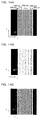
図6Aは、元のサンプルパターンの具体例を示す図である。図6Bは、顕微鏡100において構造照明を用いない場合に達成される解像の結果を説明する図であり、図6Cは、実施形態の顕微鏡100において構造照明を用いて達成される超解像の結果を説明する図である。横軸は位置を示し、縦軸は散乱効率を示す。縦軸は試料の存在を示す指標として散乱のしやすさの度合いとしての散乱効率を表すが、一様強度照明下の観察像の曲線については、これに代えて像強度分布をプロットしている。元のサンプルパターン(図6B及び6Cでは破線)は、100nm間隔から900nm間隔まで50nm単位で間隔を増加させたものとなっている。
図7Aは、図6Aに示すサンプルパターンに対して構造照明や一様強度照明を行った場合の結像電場分布を説明するグラフである。横軸は位置を示し、縦軸は電場の値を示す。このシミュレーションにおいて、コヒーレント光源10から射出させるレーザ光L1の波長λを488nmとし、入射角度θを45度とし、対物レンズ45のNAを0.4としている。実線及び破線は、位相を変えた第1及び第2構造照明下で取得した画像に対応するものであり、点線又は薄い線は、一様強度照明で取得した画像に対応するものである。図7Bは、再現されたサンプルの空間周波数成分を説明するグラフである。中央にピークを有する実線が一様強度照明によって得た空間周波数成分であり、左右にピークを有する破線が構造照明を利用して得た空間周波数成分であり、点線で表されたサンプルが本来持っている周波数成分が概ね復元されていることがわかる。
顕微鏡によって取得可能な最大空間周波数は、一般的な一様強度照明では、波長をλとして、NA/λとなる。一方、実施形態の顕微鏡100で達成される最小空間周波数は、NA/λ+sinθ/λとなる。波長λを488nmとし、入射角度θを45度とした場合、一般的な一様強度照明では、解像可能な間隔が1220nmとなり、実施形態の顕微鏡100では、解像可能な間隔が440nmとなることを意味する。一般的な一様強度照明によって再構成された画像(図6Bの実線参照)と、実施形態の構造照明を用いて結像電場分布から再構成された画像(図6Cの実線参照)とを比較すると、実施形態の構造照明によってサンプル間隔450nmあたりまで解像が可能であることが分かる。一方、一般的な一様強度照明では、900nmの間隔でさえ解像が容易でないことが分かる。
以下、近接する2点からなるサンプルの観察に関する解像(2点解像)について説明する。
図8A~8Hは、コヒーレント光源10から射出させるレーザ光L1の波長λを488nmとし、入射角度θを45度とし、対物レンズ45のNAを0.4とした場合の解像結果を示している。各グラフにおいて、横軸は位置を示し、縦軸は散乱効率を示す。ここで、一様強度照明下の観察像の曲線については、これに代えて像強度分布をプロットしている。各グラフにおいて、縦に延びる破線は、サンプルの2点ピークを示し、実線は、実施形態の構造照明を利用した解像を示し、点線又は薄い線は、一般的な一様強度照明を利用した解像を示す。以上の点は、以下の解像例でも同様であり、以下では重複説明を省略する。
図8Aは、サンプルの2点間隔が300nmの場合を示し、図8Bは、サンプルの2点間隔が320nmの場合を示し、図8Cは、サンプルの2点間隔が350nmの場合を示し、図8Dは、サンプルの2点間隔が400nmの場合を示し、図8Eは、サンプルの2点間隔が450nmの場合を示し、図8Fは、サンプルの2点間隔が500nmの場合を示し、図8Gは、サンプルの2点間隔が800nmの場合を示し、図8Hは、サンプルの2点間隔が900nmの場合を示す。解像の定義によるが、実施形態の構造照明では、図8Cに示す350nm間隔の2点についての再構成で十分な解像が達成されているが、比較例の一様強度照明では、図8Hに示す900nm間隔の2点についてさえ十分な分離ができていないことが分かる。なお、既述のように、一様強度照明では、理論的に解像可能な間隔が1220nmとなり、実施形態の顕微鏡100では、理論的に解像可能な間隔が440nmとなるので、上記図示の解像結果は理論的分解能と整合している。
図9A~9H及び図10A及び10Bは、コヒーレント光源10から射出させるレーザ光L1の波長λを488nmとし、入射角度θを60度とし、対物レンズ45のNAを0.5とした場合の解像結果を示している。図9Aは、サンプルの2点間隔が200nmの場合を示し、図9Bは、サンプルの2点間隔が250nmの場合を示し、図9Cは、サンプルの2点間隔が300nmの場合を示し、図9Dは、サンプルの2点間隔が320nmの場合を示し、図9Eは、サンプルの2点間隔が350nmの場合を示し、図9Fは、サンプルの2点間隔が400nmの場合を示し、図9Gは、サンプルの2点間隔が500nmの場合を示し、図9Hは、サンプルの2点間隔が600nmの場合を示す。また、図10Aは、サンプルの2点間隔が700nmの場合を示し、図10Bは、サンプルの2点間隔が800nmの場合を示す。各グラフにおいて、破線は、サンプルの2点ピークを示し、実線は、実施形態の構造照明を利用した解像を示し、点線又は薄い線は、一般的な一様強度照明を利用した解像を示す。実施形態の構造照明では、図9Cに示す300nm間隔の2点についての再構成で十分な解像が達成されているが、比較例の一様強度照明では、図10Aに示す700nm間隔の2点についてさえ十分な分離ができていないことが分かる。なお、上記波長λ、入射角度θ、NAを前提とした場合、一様強度照明では、理論的に解像可能な間隔が976nmとなり、実施形態の顕微鏡100では、理論的に解像可能な間隔が357nmとなるので、上記図示の解像結果は理論的分解能と整合している。
図11A~11Gは、コヒーレント光源10から射出させるレーザ光L1の波長λを488nmとし、入射角度θを80度とし、対物レンズ45のNAを0.6とした場合の解像結果を示している。図11Aは、サンプルの2点間隔が200nmの場合を示し、図11Bは、サンプルの2点間隔が250nmの場合を示し、図11Cは、サンプルの2点間隔が300nmの場合を示し、図11Dは、サンプルの2点間隔が400nmの場合を示し、図11Eは、サンプルの2点間隔が500nmの場合を示し、図11Fは、サンプルの2点間隔が600nmの場合を示し、図11Gは、サンプルの2点間隔が700nmの場合を示す。各グラフにおいて、破線は、サンプルの2点ピークを示し、実線は、実施形態の構造照明を利用した解像を示し、点線又は薄い線は、一般的な一様強度照明を利用した解像を示す。実施形態の構造照明では、図11Bに示す250nm間隔の2点についての再構成で十分な解像が達成されているが、比較例の一様強度照明では、図11Fに示す600nm間隔の2点についてさえ十分な分離ができていないことが分かる。なお、上記波長λ、入射角度θ、NAを前提とした場合、一様強度照明では、理論的に解像可能な間隔が813nmとなり、実施形態の顕微鏡100では、理論的に解像可能な間隔が307nmとなるので、上記図示の解像結果は理論的分解能と整合している。
図12A~12Gは、コヒーレント光源10から射出させるレーザ光L1の波長λを488nmとし、入射角度θを80度とし、対物レンズ45のNAを0.7とした場合の解像結果を示している。図12Aは、サンプルの2点間隔が200nmの場合を示し、図12Bは、サンプルの2点間隔が250nmの場合を示し、図12Cは、サンプルの2点間隔が300nmの場合を示し、図12Dは、サンプルの2点間隔が400nmの場合を示し、図12Eは、サンプルの2点間隔が500nmの場合を示し、図12Fは、サンプルの2点間隔が550nmの場合を示し、図12Gは、サンプルの2点間隔が600nmの場合を示す。各グラフにおいて、破線は、サンプルの2点ピークを示し、実線は、実施形態の構造照明を利用した解像を示し、点線又は薄い線は、一般的な一様強度照明を利用した解像を示す。実施形態の構造照明では、図12Bに示す250nm間隔の2点についての再構成で十分な解像が達成されているが、比較例の一様強度照明では、図12Fに示す550nm間隔の2点についてさえ十分な分離ができていないことが分かる。なお、上記波長λ、入射角度θ、NAを前提とした場合、一様強度照明では、理論的に解像可能な間隔が697nmとなり、実施形態の顕微鏡100では、理論的に解像可能な間隔が289nmとなるので、上記図示の解像結果は理論的分解能と整合している。
図13A~13Fは、コヒーレント光源10から射出させるレーザ光L1の波長λを488nmとし、入射角度θを80度とし、対物レンズ45のNAを0.95とした場合の解像結果を示している。図13Aは、サンプルの2点間隔が150nmの場合を示し、図13Bは、サンプルの2点間隔が180nmの場合を示し、図13Cは、サンプルの2点間隔が200nmの場合を示し、図13Dは、サンプルの2点間隔が300nmの場合を示し、図13Eは、サンプルの2点間隔が350nmの場合を示し、図13Fは、サンプルの2点間隔が400nmの場合を示す。各グラフにおいて、破線は、サンプルの2点ピークを示し、実線は、実施形態の構造照明を利用した解像を示し、点線又は薄い線は、一般的な一様強度照明を利用した解像を示す。実施形態の構造照明では、図13Cに示す200nm間隔の2点についての再構成で十分な解像が達成されているが、比較例の一様強度照明では、図13Eに示す350nm間隔の2点についてさえ分離があまり明確でないことが分かる。なお、上記波長λ、入射角度θ、NAを前提とした場合、一様強度照明では、理論的に解像可能な間隔が426nmとなり、実施形態の顕微鏡100では、理論的に解像可能な間隔が209nmとなるので、上記図示の解像結果は理論的分解能と整合している。
図14A~14Cは、図6A~6Cに対応する2次元のシミュレーション結果を説明する図である。図14Aは、図6Aに対応し元のサンプルパターンの具体例を示す図であり、元のサンプルパターンは、x方向の間隔を徐々に増加させたストライプパターンである。図14Bは、顕微鏡100において構造照明を用いない場合に達成される2次元解像の結果を説明する図であり、図14Cは、実施形態の顕微鏡100において構造照明を用いて達成される2次元解像の結果を説明する図である。このシミュレーションにおいて、コヒーレント光源10から射出させるレーザ光L1の波長λを488nmとし、入射角度θを45度とし、対物レンズ45のNAを0.4としている。図14Cから明らかなように、実施形態の構造照明によってサンプル間隔450nmあたりまで解像が可能であることが分かる。この結果は、実施形態の顕微鏡100によって理論的に解像可能な間隔が440nmであることと整合している。
以上では、実施形態の顕微鏡等について説明したが、本発明に係る顕微鏡等は上記のものには限られない。例えば、照明パターン(構造照明)IPの周期方向は、x方向に限らず任意の方向とでき、周期方向を任意の複数方向に設定した構造照明を行うこともでき、今回の手法を適用することで任意の方向(単一方向に限らない)の解像力を向上させることができる。具体的には例えば、x方向だけでなくy方向に関しても実施形態のような構造照明を行って、各方向の構造照明について結像電場分布のフーリエ変換から各方向に関して一対の空間周波数情報を得る。さらに、x方向及びy方向ごとに得た一対の空間周波数情報と、一様強度分布照明による結像電場分布から得た空間周波数情報とを結合することにより、x方向及びy方向に関して解像度を向上させた超解像画像を得ることができる。
以上の説明では、単一タイプの構造照明下で得た結像電場分布から算出した超解像の空間周波数の信号成分を、一様強度照明下で得た結像電場分布に対応する通常解像の空間周波数の信号成分に対して部分的に重複させることで局所的な途切れがない空間周波数情報又は空間周波数分布を得ているが、複数タイプの構造照明下で得た結像電場分布を組み合わせることもできる。つまり、空間周波数が大小異なる構造照明下で得た結像電場分布から算出した2段階の超解像の空間周波数の信号成分を繋ぎ合わせるとともに、一様強度照明下で得た結像電場分布に対応する通常解像の空間周波数の信号成分をさらに繋ぎ合わせることで、広範囲に亘って途切れがない空間周波数情報を得ることができる。
以上で説明した実施形態では、顕微鏡100に基本光照射部40を組み込んでいたが、基本光照射部40は、必須のものではなく省略することができる。
構造照明用の光L21,L22は、対物レンズ45を挟んで互いに反対側から入射させるもの、或いは対物レンズ45の光軸を挟んで互いに反対側から入射させるものであれば正確に対称に配置されたものでなくても足る。つまり、構造照明用の光L21,L22の入射角θは等しくなくてもよいが、光L21,L22の強度は解像の信頼性を高める観点から等しいことが望ましい。
また、構造照明については、斜入射させる光L21,L22の相対的位相をシフトさせるだけでなく、試料面88aとなるべきステージ88自体を強弱パターンが繰り返されるx方向にシフトさせることによっても達成可能である。
以上の説明では、参照用の光L3による電場シフトに対応して光検出部60によって検出される光強度の増減から結像電場分布を正負の符号を含めて見積もっているが(図3A~3C参照)、電場シフトに対応して光検出部60によって検出される光強度の増減量の程度から結像電場分布を正負の符号を含めて見積もることもできる。
Claims (13)
- コヒーレント光源と、
前記コヒーレント光源から構造照明用の光を分岐して略対称的な一対の斜め方向から試料位置に照射する構造照明部と、
前記試料位置から射出された散乱光の分布を対物レンズを介して検出する光検出部と、
前記コヒーレント光源から参照用の光を分岐して前記光検出部の検出面に照射することによって一様な電場シフトを与える参照光照射部と、
を備える顕微鏡。 - 前記参照光照射部は、前記構造照明部によって照明された前記試料位置から射出され前記光検出部の前記検出面に形成された散乱パターンに位相の異なる参照用の光を干渉させる、請求項1に記載の顕微鏡。
- 前記参照光照射部は、前記光検出部の前記検出面上の前記散乱パターンに重ねて初期位相状態の平面波と、前記初期位相状態とは異なる位相状態の平面波とを順次照射する、請求項2に記載の顕微鏡。
- 前記一様な電場シフトに対応して前記光検出部によって検出される光強度の増減から結像電場分布を正負の符号を含めて見積もる、請求項1~3のいずれか一項に記載の顕微鏡。
- 前記構造照明部は、前記試料位置に形成される光の空間的な照明パターンとしての前記構造照明をシフトさせる、請求項1~4のいずれか一項に記載の顕微鏡。
- 前記構造照明部は、前記一対の斜め方向から照射する光の位相を相対的にシフトさせる、請求項5に記載の顕微鏡。
- 前記構造照明部は、前記試料位置に一対の平面波を照射することによって構造照明を形成する、請求項6に記載の顕微鏡。
- 前記一対の斜め方向から照射する光は、強度が等しい、請求項5~7のいずれか一項に記載の顕微鏡。
- 前記コヒーレント光源から通常照明用の光を分岐して前記対物レンズ越しに前記試料位置に照射する基本光照射部をさらに備える、請求項1~8のいずれか一項に記載の顕微鏡。
- 前記基本光照射部は、前記構造照明部による構造照明がない状態で前記試料位置に平面波を照射する、請求項9に記載の顕微鏡。
- 前記構造照明部及び前記参照光照射部を動作させて前記光検出部によって検出した結像電場分布と、前記基本光照射部を動作させて前記光検出部によって検出した結像電場分布とに基いて、前記構造照明の空間周波数に対応させて空間周波数帯域を拡張した画像を再構成する演算処理部をさらに備える、請求項9及び10のいずれか一項に記載の顕微鏡。
- コヒーレント光源からの光を分岐して略対称的な一対の斜め方向から試料位置に照射する構造照明部と、前記試料位置から射出された散乱光の分布を対物レンズを介して検出する光検出部と、前記コヒーレント光源から参照用の光を分岐して前記光検出部の検出面に照射する参照光照射部と、を備える顕微鏡を用いた顕微法であって、
前記試料位置において一対の構造照明を照射して散乱光を取り出すとともに、前記光検出部の検出面で前記参照用の光を干渉させることによって一様な電場シフトを与え、結像電場分布に相当する信号を取得する工程と、
前記一対の構造照明下で得た結像電場分布に相当する信号のフーリエ変換から拡張空間周波数情報を抽出し、逆フーリエ変換することによって、試料像を再構成する、顕微法。 - 前記顕微鏡は、前記コヒーレント光源から通常照明用の光を分岐して前記対物レンズ越しに前記試料位置に照射する基本光照射部をさらに備え、
前記拡張空間周波数情報と、通常照明下で検出した信号のフーリエ変換から得た基本空間周波数情報とを合成し、逆フーリエ変換することによって、試料像を再構成する、請求項12に記載の顕微法。
Applications Claiming Priority (2)
| Application Number | Priority Date | Filing Date | Title |
|---|---|---|---|
| JP2018-199590 | 2018-10-23 | ||
| JP2018199590A JP2020067538A (ja) | 2018-10-23 | 2018-10-23 | 顕微鏡及び顕微法 |
Publications (1)
| Publication Number | Publication Date |
|---|---|
| WO2020085402A1 true WO2020085402A1 (ja) | 2020-04-30 |
Family
ID=70332035
Family Applications (1)
| Application Number | Title | Priority Date | Filing Date |
|---|---|---|---|
| PCT/JP2019/041575 Ceased WO2020085402A1 (ja) | 2018-10-23 | 2019-10-23 | 顕微鏡及び顕微法 |
Country Status (2)
| Country | Link |
|---|---|
| JP (1) | JP2020067538A (ja) |
| WO (1) | WO2020085402A1 (ja) |
Citations (5)
| Publication number | Priority date | Publication date | Assignee | Title |
|---|---|---|---|---|
| WO2013125723A1 (ja) * | 2012-02-24 | 2013-08-29 | 国立大学法人東京大学 | 照明方法および顕微観察装置 |
| WO2015033394A1 (ja) * | 2013-09-04 | 2015-03-12 | 株式会社日立製作所 | 光断層観察装置 |
| US20150077535A1 (en) * | 2013-04-12 | 2015-03-19 | Duke University | Systems and methods for structured illumination super-resolution phase microscopy |
| US20150177133A1 (en) * | 2007-07-10 | 2015-06-25 | Massachusetts Institute Of Technology | Tomographic phase microscopy |
| JP2017102068A (ja) * | 2015-12-03 | 2017-06-08 | リオン株式会社 | パーティクルカウンタ |
-
2018
- 2018-10-23 JP JP2018199590A patent/JP2020067538A/ja active Pending
-
2019
- 2019-10-23 WO PCT/JP2019/041575 patent/WO2020085402A1/ja not_active Ceased
Patent Citations (5)
| Publication number | Priority date | Publication date | Assignee | Title |
|---|---|---|---|---|
| US20150177133A1 (en) * | 2007-07-10 | 2015-06-25 | Massachusetts Institute Of Technology | Tomographic phase microscopy |
| WO2013125723A1 (ja) * | 2012-02-24 | 2013-08-29 | 国立大学法人東京大学 | 照明方法および顕微観察装置 |
| US20150077535A1 (en) * | 2013-04-12 | 2015-03-19 | Duke University | Systems and methods for structured illumination super-resolution phase microscopy |
| WO2015033394A1 (ja) * | 2013-09-04 | 2015-03-12 | 株式会社日立製作所 | 光断層観察装置 |
| JP2017102068A (ja) * | 2015-12-03 | 2017-06-08 | リオン株式会社 | パーティクルカウンタ |
Non-Patent Citations (1)
| Title |
|---|
| KUME, HIROMASA ET AL.: "Super-resolution optical for semiconductor defects using standing wave shift (22nd report", LECTURE PROCEEDINGS OF ACADEMIC LECTURE CONFERENCE OF 2017 JSPE AUTUMN CONFERENCE, 5 September 2017 (2017-09-05), pages 201 - 202 * |
Also Published As
| Publication number | Publication date |
|---|---|
| JP2020067538A (ja) | 2020-04-30 |
Similar Documents
| Publication | Publication Date | Title |
|---|---|---|
| TWI797377B (zh) | 表面形狀量測裝置以及表面形狀量測方法 | |
| US8319975B2 (en) | Methods and apparatus for wavefront manipulations and improved 3-D measurements | |
| US7808648B2 (en) | Method and device for optical determination of physical properties of features, not much larger than the optical wavelength used, on a test sample | |
| US7312875B2 (en) | Two-wavelength spatial-heterodyne holography | |
| US10635049B2 (en) | Ellipsometry device and ellipsometry method | |
| US20110149298A1 (en) | Spatial wavefront analysis and 3d measurement | |
| JP2000510951A (ja) | 光学測定 | |
| JP7432227B2 (ja) | 位相イメージング装置、位相イメージング方法 | |
| EP3674698B1 (en) | Inspection apparatus and inspection method | |
| CN108931207A (zh) | Led照明的干涉显微装置和方法 | |
| JP5428538B2 (ja) | 干渉装置 | |
| KR101547459B1 (ko) | 위상 축소 이미징 시스템 및 이를 이용한 이미징 방법 | |
| JP6230358B2 (ja) | 光学的距離計測装置 | |
| CN116300364B (zh) | 一种基于部分相干光照明的定量相衬显微成像装置 | |
| Gao et al. | Interface and spectrum multiplexing ptychographic reflection microscopy | |
| KR100871270B1 (ko) | 광학 간섭계를 이용한 샘플 시료의 이미지 정보 생성 방법및 장치 | |
| CN108120393B (zh) | 一种多光场调制的三维形貌测量方法 | |
| US7864327B1 (en) | In-phase/in-quadrature demodulator for spectral information of interference signal | |
| JP2020067538A (ja) | 顕微鏡及び顕微法 | |
| JP5454769B2 (ja) | 分光立体形状測定装置及び分光立体形状測定方法 | |
| CN208595888U (zh) | 一种稳定的轻离轴干涉显微装置 | |
| CN110763686A (zh) | 一种透明样品的缺陷检测装置和检测方法 | |
| Zhao et al. | Slightly off-axis digital holographic microscopy with a divided aperture | |
| CN110715931B (zh) | 一种透明样品缺陷自动检测方法和检测装置 | |
| US12467737B1 (en) | Self-referencing interferometric microscope |
Legal Events
| Date | Code | Title | Description |
|---|---|---|---|
| 121 | Ep: the epo has been informed by wipo that ep was designated in this application |
Ref document number: 19877315 Country of ref document: EP Kind code of ref document: A1 |
|
| NENP | Non-entry into the national phase |
Ref country code: DE |
|
| 122 | Ep: pct application non-entry in european phase |
Ref document number: 19877315 Country of ref document: EP Kind code of ref document: A1 |