WO2020082891A1 - 一种显示装置、显示面板及其电容补偿的方法 - Google Patents
一种显示装置、显示面板及其电容补偿的方法 Download PDFInfo
- Publication number
- WO2020082891A1 WO2020082891A1 PCT/CN2019/103160 CN2019103160W WO2020082891A1 WO 2020082891 A1 WO2020082891 A1 WO 2020082891A1 CN 2019103160 W CN2019103160 W CN 2019103160W WO 2020082891 A1 WO2020082891 A1 WO 2020082891A1
- Authority
- WO
- WIPO (PCT)
- Prior art keywords
- display area
- row
- capacitance
- scanning lines
- compensation
- Prior art date
- Legal status (The legal status is an assumption and is not a legal conclusion. Google has not performed a legal analysis and makes no representation as to the accuracy of the status listed.)
- Ceased
Links
Images




Classifications
-
- G—PHYSICS
- G09—EDUCATION; CRYPTOGRAPHY; DISPLAY; ADVERTISING; SEALS
- G09G—ARRANGEMENTS OR CIRCUITS FOR CONTROL OF INDICATING DEVICES USING STATIC MEANS TO PRESENT VARIABLE INFORMATION
- G09G3/00—Control arrangements or circuits, of interest only in connection with visual indicators other than cathode-ray tubes
- G09G3/20—Control arrangements or circuits, of interest only in connection with visual indicators other than cathode-ray tubes for presentation of an assembly of a number of characters, e.g. a page, by composing the assembly by combination of individual elements arranged in a matrix no fixed position being assigned to or needed to be assigned to the individual characters or partial characters
- G09G3/22—Control arrangements or circuits, of interest only in connection with visual indicators other than cathode-ray tubes for presentation of an assembly of a number of characters, e.g. a page, by composing the assembly by combination of individual elements arranged in a matrix no fixed position being assigned to or needed to be assigned to the individual characters or partial characters using controlled light sources
- G09G3/30—Control arrangements or circuits, of interest only in connection with visual indicators other than cathode-ray tubes for presentation of an assembly of a number of characters, e.g. a page, by composing the assembly by combination of individual elements arranged in a matrix no fixed position being assigned to or needed to be assigned to the individual characters or partial characters using controlled light sources using electroluminescent panels
- G09G3/32—Control arrangements or circuits, of interest only in connection with visual indicators other than cathode-ray tubes for presentation of an assembly of a number of characters, e.g. a page, by composing the assembly by combination of individual elements arranged in a matrix no fixed position being assigned to or needed to be assigned to the individual characters or partial characters using controlled light sources using electroluminescent panels semiconductive, e.g. using light-emitting diodes [LED]
- G09G3/3208—Control arrangements or circuits, of interest only in connection with visual indicators other than cathode-ray tubes for presentation of an assembly of a number of characters, e.g. a page, by composing the assembly by combination of individual elements arranged in a matrix no fixed position being assigned to or needed to be assigned to the individual characters or partial characters using controlled light sources using electroluminescent panels semiconductive, e.g. using light-emitting diodes [LED] organic, e.g. using organic light-emitting diodes [OLED]
- G09G3/3225—Control arrangements or circuits, of interest only in connection with visual indicators other than cathode-ray tubes for presentation of an assembly of a number of characters, e.g. a page, by composing the assembly by combination of individual elements arranged in a matrix no fixed position being assigned to or needed to be assigned to the individual characters or partial characters using controlled light sources using electroluminescent panels semiconductive, e.g. using light-emitting diodes [LED] organic, e.g. using organic light-emitting diodes [OLED] using an active matrix
-
- G—PHYSICS
- G02—OPTICS
- G02F—OPTICAL DEVICES OR ARRANGEMENTS FOR THE CONTROL OF LIGHT BY MODIFICATION OF THE OPTICAL PROPERTIES OF THE MEDIA OF THE ELEMENTS INVOLVED THEREIN; NON-LINEAR OPTICS; FREQUENCY-CHANGING OF LIGHT; OPTICAL LOGIC ELEMENTS; OPTICAL ANALOGUE/DIGITAL CONVERTERS
- G02F1/00—Devices or arrangements for the control of the intensity, colour, phase, polarisation or direction of light arriving from an independent light source, e.g. switching, gating or modulating; Non-linear optics
- G02F1/01—Devices or arrangements for the control of the intensity, colour, phase, polarisation or direction of light arriving from an independent light source, e.g. switching, gating or modulating; Non-linear optics for the control of the intensity, phase, polarisation or colour
- G02F1/13—Devices or arrangements for the control of the intensity, colour, phase, polarisation or direction of light arriving from an independent light source, e.g. switching, gating or modulating; Non-linear optics for the control of the intensity, phase, polarisation or colour based on liquid crystals, e.g. single liquid crystal display cells
- G02F1/133—Constructional arrangements; Operation of liquid crystal cells; Circuit arrangements
- G02F1/136—Liquid crystal cells structurally associated with a semi-conducting layer or substrate, e.g. cells forming part of an integrated circuit
- G02F1/1362—Active matrix addressed cells
- G02F1/136286—Wiring, e.g. gate line, drain line
-
- G—PHYSICS
- G02—OPTICS
- G02F—OPTICAL DEVICES OR ARRANGEMENTS FOR THE CONTROL OF LIGHT BY MODIFICATION OF THE OPTICAL PROPERTIES OF THE MEDIA OF THE ELEMENTS INVOLVED THEREIN; NON-LINEAR OPTICS; FREQUENCY-CHANGING OF LIGHT; OPTICAL LOGIC ELEMENTS; OPTICAL ANALOGUE/DIGITAL CONVERTERS
- G02F1/00—Devices or arrangements for the control of the intensity, colour, phase, polarisation or direction of light arriving from an independent light source, e.g. switching, gating or modulating; Non-linear optics
- G02F1/01—Devices or arrangements for the control of the intensity, colour, phase, polarisation or direction of light arriving from an independent light source, e.g. switching, gating or modulating; Non-linear optics for the control of the intensity, phase, polarisation or colour
- G02F1/13—Devices or arrangements for the control of the intensity, colour, phase, polarisation or direction of light arriving from an independent light source, e.g. switching, gating or modulating; Non-linear optics for the control of the intensity, phase, polarisation or colour based on liquid crystals, e.g. single liquid crystal display cells
- G02F1/133—Constructional arrangements; Operation of liquid crystal cells; Circuit arrangements
- G02F1/1333—Constructional arrangements; Manufacturing methods
- G02F1/13338—Input devices, e.g. touch panels
-
- G—PHYSICS
- G09—EDUCATION; CRYPTOGRAPHY; DISPLAY; ADVERTISING; SEALS
- G09G—ARRANGEMENTS OR CIRCUITS FOR CONTROL OF INDICATING DEVICES USING STATIC MEANS TO PRESENT VARIABLE INFORMATION
- G09G3/00—Control arrangements or circuits, of interest only in connection with visual indicators other than cathode-ray tubes
- G09G3/20—Control arrangements or circuits, of interest only in connection with visual indicators other than cathode-ray tubes for presentation of an assembly of a number of characters, e.g. a page, by composing the assembly by combination of individual elements arranged in a matrix no fixed position being assigned to or needed to be assigned to the individual characters or partial characters
- G09G3/22—Control arrangements or circuits, of interest only in connection with visual indicators other than cathode-ray tubes for presentation of an assembly of a number of characters, e.g. a page, by composing the assembly by combination of individual elements arranged in a matrix no fixed position being assigned to or needed to be assigned to the individual characters or partial characters using controlled light sources
- G09G3/30—Control arrangements or circuits, of interest only in connection with visual indicators other than cathode-ray tubes for presentation of an assembly of a number of characters, e.g. a page, by composing the assembly by combination of individual elements arranged in a matrix no fixed position being assigned to or needed to be assigned to the individual characters or partial characters using controlled light sources using electroluminescent panels
- G09G3/32—Control arrangements or circuits, of interest only in connection with visual indicators other than cathode-ray tubes for presentation of an assembly of a number of characters, e.g. a page, by composing the assembly by combination of individual elements arranged in a matrix no fixed position being assigned to or needed to be assigned to the individual characters or partial characters using controlled light sources using electroluminescent panels semiconductive, e.g. using light-emitting diodes [LED]
- G09G3/3208—Control arrangements or circuits, of interest only in connection with visual indicators other than cathode-ray tubes for presentation of an assembly of a number of characters, e.g. a page, by composing the assembly by combination of individual elements arranged in a matrix no fixed position being assigned to or needed to be assigned to the individual characters or partial characters using controlled light sources using electroluminescent panels semiconductive, e.g. using light-emitting diodes [LED] organic, e.g. using organic light-emitting diodes [OLED]
- G09G3/3266—Details of drivers for scan electrodes
-
- G—PHYSICS
- G09—EDUCATION; CRYPTOGRAPHY; DISPLAY; ADVERTISING; SEALS
- G09G—ARRANGEMENTS OR CIRCUITS FOR CONTROL OF INDICATING DEVICES USING STATIC MEANS TO PRESENT VARIABLE INFORMATION
- G09G3/00—Control arrangements or circuits, of interest only in connection with visual indicators other than cathode-ray tubes
- G09G3/20—Control arrangements or circuits, of interest only in connection with visual indicators other than cathode-ray tubes for presentation of an assembly of a number of characters, e.g. a page, by composing the assembly by combination of individual elements arranged in a matrix no fixed position being assigned to or needed to be assigned to the individual characters or partial characters
- G09G3/34—Control arrangements or circuits, of interest only in connection with visual indicators other than cathode-ray tubes for presentation of an assembly of a number of characters, e.g. a page, by composing the assembly by combination of individual elements arranged in a matrix no fixed position being assigned to or needed to be assigned to the individual characters or partial characters by control of light from an independent source
- G09G3/36—Control arrangements or circuits, of interest only in connection with visual indicators other than cathode-ray tubes for presentation of an assembly of a number of characters, e.g. a page, by composing the assembly by combination of individual elements arranged in a matrix no fixed position being assigned to or needed to be assigned to the individual characters or partial characters by control of light from an independent source using liquid crystals
- G09G3/3611—Control of matrices with row and column drivers
- G09G3/3674—Details of drivers for scan electrodes
-
- H—ELECTRICITY
- H10—SEMICONDUCTOR DEVICES; ELECTRIC SOLID-STATE DEVICES NOT OTHERWISE PROVIDED FOR
- H10K—ORGANIC ELECTRIC SOLID-STATE DEVICES
- H10K59/00—Integrated devices, or assemblies of multiple devices, comprising at least one organic light-emitting element covered by group H10K50/00
-
- G—PHYSICS
- G09—EDUCATION; CRYPTOGRAPHY; DISPLAY; ADVERTISING; SEALS
- G09G—ARRANGEMENTS OR CIRCUITS FOR CONTROL OF INDICATING DEVICES USING STATIC MEANS TO PRESENT VARIABLE INFORMATION
- G09G2300/00—Aspects of the constitution of display devices
- G09G2300/04—Structural and physical details of display devices
- G09G2300/0421—Structural details of the set of electrodes
- G09G2300/0426—Layout of electrodes and connections
-
- G—PHYSICS
- G09—EDUCATION; CRYPTOGRAPHY; DISPLAY; ADVERTISING; SEALS
- G09G—ARRANGEMENTS OR CIRCUITS FOR CONTROL OF INDICATING DEVICES USING STATIC MEANS TO PRESENT VARIABLE INFORMATION
- G09G2310/00—Command of the display device
- G09G2310/02—Addressing, scanning or driving the display screen or processing steps related thereto
- G09G2310/0202—Addressing of scan or signal lines
- G09G2310/0221—Addressing of scan or signal lines with use of split matrices
-
- G—PHYSICS
- G09—EDUCATION; CRYPTOGRAPHY; DISPLAY; ADVERTISING; SEALS
- G09G—ARRANGEMENTS OR CIRCUITS FOR CONTROL OF INDICATING DEVICES USING STATIC MEANS TO PRESENT VARIABLE INFORMATION
- G09G2320/00—Control of display operating conditions
- G09G2320/02—Improving the quality of display appearance
- G09G2320/0223—Compensation for problems related to R-C delay and attenuation in electrodes of matrix panels, e.g. in gate electrodes or on-substrate video signal electrodes
-
- G—PHYSICS
- G09—EDUCATION; CRYPTOGRAPHY; DISPLAY; ADVERTISING; SEALS
- G09G—ARRANGEMENTS OR CIRCUITS FOR CONTROL OF INDICATING DEVICES USING STATIC MEANS TO PRESENT VARIABLE INFORMATION
- G09G2320/00—Control of display operating conditions
- G09G2320/02—Improving the quality of display appearance
- G09G2320/0233—Improving the luminance or brightness uniformity across the screen
-
- G—PHYSICS
- G09—EDUCATION; CRYPTOGRAPHY; DISPLAY; ADVERTISING; SEALS
- G09G—ARRANGEMENTS OR CIRCUITS FOR CONTROL OF INDICATING DEVICES USING STATIC MEANS TO PRESENT VARIABLE INFORMATION
- G09G3/00—Control arrangements or circuits, of interest only in connection with visual indicators other than cathode-ray tubes
- G09G3/20—Control arrangements or circuits, of interest only in connection with visual indicators other than cathode-ray tubes for presentation of an assembly of a number of characters, e.g. a page, by composing the assembly by combination of individual elements arranged in a matrix no fixed position being assigned to or needed to be assigned to the individual characters or partial characters
- G09G3/34—Control arrangements or circuits, of interest only in connection with visual indicators other than cathode-ray tubes for presentation of an assembly of a number of characters, e.g. a page, by composing the assembly by combination of individual elements arranged in a matrix no fixed position being assigned to or needed to be assigned to the individual characters or partial characters by control of light from an independent source
- G09G3/36—Control arrangements or circuits, of interest only in connection with visual indicators other than cathode-ray tubes for presentation of an assembly of a number of characters, e.g. a page, by composing the assembly by combination of individual elements arranged in a matrix no fixed position being assigned to or needed to be assigned to the individual characters or partial characters by control of light from an independent source using liquid crystals
- G09G3/3611—Control of matrices with row and column drivers
- G09G3/3648—Control of matrices with row and column drivers using an active matrix
-
- H—ELECTRICITY
- H10—SEMICONDUCTOR DEVICES; ELECTRIC SOLID-STATE DEVICES NOT OTHERWISE PROVIDED FOR
- H10K—ORGANIC ELECTRIC SOLID-STATE DEVICES
- H10K59/00—Integrated devices, or assemblies of multiple devices, comprising at least one organic light-emitting element covered by group H10K50/00
- H10K59/10—OLED displays
- H10K59/12—Active-matrix OLED [AMOLED] displays
- H10K59/121—Active-matrix OLED [AMOLED] displays characterised by the geometry or disposition of pixel elements
- H10K59/1216—Active-matrix OLED [AMOLED] displays characterised by the geometry or disposition of pixel elements the pixel elements being capacitors
-
- H—ELECTRICITY
- H10—SEMICONDUCTOR DEVICES; ELECTRIC SOLID-STATE DEVICES NOT OTHERWISE PROVIDED FOR
- H10K—ORGANIC ELECTRIC SOLID-STATE DEVICES
- H10K59/00—Integrated devices, or assemblies of multiple devices, comprising at least one organic light-emitting element covered by group H10K50/00
- H10K59/10—OLED displays
- H10K59/12—Active-matrix OLED [AMOLED] displays
- H10K59/131—Interconnections, e.g. wiring lines or terminals
Definitions
- the present application relates to the technical field of display equipment, and in particular, to a display device, a display panel, and a method of capacitance compensation.
- OLED Organic Light Emitting Diode
- the display panel When the display panel is applied to mobile terminal products, it may be necessary to set up mounting holes in the display area to reserve the installation location of hardware such as a front camera, earpiece, or home button on the mobile terminal device.
- the number of pixel units in the row where the mounting holes are located is less than the number of pixel units in the row where the mounting holes are not provided. This causes bright and dark stripes in the display area, that is, the problem of uneven display brightness.
- the present application provides a display device, a display panel, and a capacitance compensation method thereof, which can solve the problem of uneven display brightness in a display area with fewer pixel units.
- a display panel includes: a first display area and a second display area adjacent to each other, the first display area and the second display area both include: a pixel array formed by a plurality of pixel units, and a plurality of rows of scanning lines, the pixel array It includes several rows of pixel units, and each row of scanning lines in the row of scanning lines drives the corresponding row of pixel units in the row of pixel units respectively;
- Each row of pixel units in the second display area has the same number of pixel units, each row of pixel units in the first display area has fewer pixel units than the pixel units in each row of pixel units in the second display area,
- Each row of scanning lines of the first display area is connected with a compensation capacitor, and the sum of the self-capacitance load value of each row of scanning lines and the compensation capacitance value of the compensation capacitor connected thereto is the total capacitance load value of the row of scanning lines;
- the total load value of the row of scanning lines adjacent to the second display area is equal to the self-capacitance load value of the row of scanning lines in the second display area.
- the total load value of the capacitance of the scanning lines in the second display area gradually decreases.
- a display device includes any one of the above display panels.
- a capacitance compensation method is applied to a display panel including a first display area and a second display area adjacent to each other; both the first display area and the second display area include: a pixel array formed by several pixel units, And a plurality of rows of scanning lines, the pixel array includes a plurality of rows of pixel units, and each row of the plurality of rows of scanning lines respectively drives a corresponding row of pixel units of the plurality of rows of pixel units;
- Each row of pixel units in the second display area has the same number of pixel units, each row of pixel units in the first display area has fewer pixel units than the pixel units in each row of pixel units in the second display area,
- Each row of scanning lines of the first display area is connected with a compensation capacitor, and the sum of the self-capacitance load value of each row of scanning lines and the compensation capacitance value of the compensation capacitor connected thereto is the total capacitance load value of the row of scanning lines;
- the capacitance compensation method includes steps:
- Capacitance compensation is performed on a row of scanning lines adjacent to the second display area in the first display area so that the total load value of the capacitance of the row of scanning lines and the self-capacitance load value of the scan lines adjacent to the row of scan lines in the second display area equal;
- Each row of scanning lines in the first display area except for the row of scanning lines adjacent to the second display area is subjected to capacitance compensation, so that the total load of the capacitance of each row of scanning lines from close to the second display area to away from the second display area The value gradually decreases.
- each row of scanning lines in the first display area except for the row of scanning lines adjacent to the second display area is subjected to capacitance compensation, so that each row from close to the second display area to far from the second display area
- the total load value of the scanning line capacitance gradually decreases, including the steps:
- This application performs capacitance compensation for each row of scanning lines in the first display area with few pixel units, and the compensation standard is: in the first display area, the total load value of the capacitance of the row of scanning lines adjacent to the second display area and the second display area
- the self-capacitance load values of the scan lines in the middle row are equal, and the total load value of the capacitance of the scan lines of each row gradually decreases from near the second display area to away from the second display area.
- the above scheme utilizes the human eye's insensitivity to the gradual change in brightness, eliminating the sudden change in the total load value of the capacitance of the scanning lines in the first display area and the boundary between the first display area and the second display area after compensation, making
- the gradual change in the total load value of the capacitors in the first display area can reduce the setting area of the compensation capacitor, which is beneficial to reduce the area of the frame area, achieve a narrow frame and increase the screen ratio.
- the total load value of the capacitance of each row of scanning lines from close to the second display area to far from the second display area shows a linear decrease or a monotonically decreasing curve.
- the human eye is less sensitive to the brightness change caused by the linear decrease.
- the first display area is located at the upper or lower part of the display panel.
- the upper or lower part of the display panel has a pixel-free area, and the pixel-free area may be an aperture area.
- the opening area may be circular, elliptical, rectangular, trapezoidal, inverted trapezoidal, triangular, bangs-shaped or irregular.
- One or a combination of functional elements such as a camera, an earpiece, a light sensor, a distance sensor, an iris recognition sensor, and a fingerprint recognition sensor can be set in the opening.
- the shape of the opening area matches the shape of the functional element provided in the opening in the opening area.
- the scan lines corresponding to the first sub-display area and the second sub-display area are disconnected in the non-pixel area, and the scan lines of the first sub-display area and the second sub-display area are each connected to a driving circuit .
- the first display area is driven bilaterally.
- the scan lines corresponding to the first sub-display area and the second sub-display area may not be disconnected in the pixel-free area, and the scan lines of the first sub-display area and the second sub-display area are connected to a driving circuit, that is : The first display area is driven unilaterally.
- the first sub-display area and the second sub-display area can be symmetrical with respect to the pixel-free area.
- the first sub-display area and the second sub-display area are scanned
- the lines can be connected with compensation capacitors respectively.
- the compensation capacitor connected to each row of scanning lines includes several compensation capacitor units connected in series.
- the advantage of the compensation capacitor unit is that the compensation capacitor unit not only has the same size but also the same size. In a limited area, such as a mobile phone screen size area, the relative error caused by the process of making the compensation capacitor unit is relatively small.
- the number of compensation capacitor units in each row is: the division value of the capacitance of the compensation capacitor connected to each row of scanning lines divided by the capacitance value of the compensation capacitor unit, or the capacitance value of the compensation capacitor connected to each row of scanning lines divided by compensation The maximum rounding multiple of the capacitance value of the capacitance unit is increased or decreased by one.
- a) the compensation capacitor is located between adjacent pixel units, and one plate of the compensation capacitor is used by the scanning line.
- This structure can omit the production of one plate, so the manufacturing process is less; or b ) The compensation capacitor is located in the border area adjacent to the first display area, or c) The compensation capacitor is located in the adjacent area between the pixel-free area and the first display area, the latter two structures can make the gap between adjacent pixel units relative to a)
- the reduction is beneficial to increase the number of pixel units and improve the resolution in a limited area. Compared with the solution in which the total load value of the capacitance of the scanning lines in each row is equal, the total load value of the capacitance of the scanning lines in the first display area shows a decreasing trend, which can reduce the installation area of the compensation capacitor.
- the other plate of the compensation capacitor is electrically connected to the power line.
- one plate of the compensation capacitor is located in the conductive layer where the scanning line is located or in the conductive layer electrically connected to the scanning line through a conductive plug; the other plate of the compensation capacitor is electrically connected to the power line.
- the other plate of the compensation capacitor can also be electrically connected to other connection lines of fixed potential, such as a common electrode line. The advantage of the electrical connection with the fixed potential connection line is that the series-parallel relationship of the compensation capacitor and the scanning line's own capacitance is fixed, which is convenient for calculating the size of the compensation capacitor.
- the compensation capacitance of the row of scanning lines farthest from the second display area in the first display area is: the self-capacitance load value of the row of scanning lines farthest from the second display area and the second The preset ratio of the difference in the self-capacitance load value of a row of scanning lines in the display area.
- the preset ratio is set according to the industry standard for uniform brightness of the display area in the display industry. Within the settable range of the preset ratio that meets industry standards, the smaller the preset ratio is, the easier it is to reduce the capacitance value of the compensation capacitor, that is, the more advantageous it is to reduce the installation area of the compensation capacitor.
- FIG. 1 is a schematic structural diagram of a display panel in an embodiment of the present application.
- FIG. 2 is a division view of each area of the display panel in FIG. 1;
- FIG. 3 is a graph showing the corresponding relationship between the self-capacitance load value of each row of scanning lines and the number of rows in the first display area;
- FIG. 5 is a graph showing the relationship between the capacitance compensation ratio of each scanning line of the first display area and the number of rows;
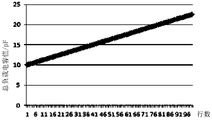
- FIG. 6 is a graph showing the corresponding relationship between the total load value of the capacitor and the number of lines after scanning line compensation in each row of the first display area;
- FIG. 8 is a schematic diagram of a two-pole plate structure of a compensation capacitor unit
- FIG. 9 is a schematic structural diagram of a display panel in another embodiment of the present application.
- the reason for the display unevenness of the display panel is that: when the structure and size of each scanning line and each pixel unit in the display panel are the same, the overlapping area of each scanning line and each pixel unit is fixed, The decrease in the number of pixel units in a row may cause the self-capacitance load value of the scanning lines in the row to be different from the self-capacitance load value of the scanning lines in other rows.
- the self-capacitance load value of the scan line refers to the capacitance value of the capacitor formed by using the scan line as one electrode plate and the other conductive layer overlapping with the scan line as another electrode plate.
- the other conductive layer may be a conductive layer in the pixel unit, such as a cathode and an anode in the OLED pixel unit, or may be a conductive layer in the pixel transistor driving the pixel unit, such as a connection line electrically connected to the source / drain, etc. .
- the unequal capacitance load means that when the control electrical signal is provided to the scan lines, the discharge current generated by the discharge process after charging each capacitor is unequal, which in turn causes a delay in the rising and falling edges of the control electrical signal on each scan line. It causes light and dark stripes during display, that is, the display brightness unevenness of each row of pixel units.
- this application applies capacitance compensation to each row of scan lines in the first display area with few pixel units, and the compensation standard is: in the first display area, the total load value of the capacitance of the row of scan lines adjacent to the second display area is equal to The self-capacitance load values of the scanning lines of one row in the second display area are equal, and the total load value of the capacitances of the scanning lines of each row from the second display area to the farther away from the second display area gradually decreases.
- the above scheme utilizes the human eye's insensitivity to the gradual change in brightness, eliminating the sudden change in the total load value of the capacitance of the scanning lines in the first display area and the boundary between the first display area and the second display area after compensation, making the display
- the gradual change in the total load value of the capacitors in the first display area can reduce the setting area of the compensation capacitor, which is beneficial to reduce the area of the frame area, achieve a narrow frame and increase the screen ratio.
- FIG. 1 is a schematic structural diagram of a display panel in an embodiment of the present application.
- FIG. 2 is a division view of each area of the display panel in FIG. 1.
- the display panel 1 includes: a first display area 11 and a second display area 12 adjacent to each other, the first display area 11 includes: a pixel array formed by a number of pixel units 10 and a number of rows Scanning lines G 1 , G 2 ... G n , the pixel array includes a plurality of rows of pixel units 10, and each of the scanning lines G 1 , G 2 ... G n corresponds to driving a corresponding row of the rows of pixel units 10 pixel unit 10; a second display area 12 comprises: a plurality of pixels of the pixel array unit 10 is formed and a plurality of scanning lines G n + 1, G n + 2 ...
- the pixel array unit 10 includes a plurality of pixel rows, a plurality of rows Each scanning line in the scanning lines G n + 1 , G n + 2 ... G m corresponds to driving a corresponding row of pixel units 10 in several rows of pixel units 10;
- Each row of pixel units 10 of the second display area 12 has the same number of pixel units, and each row of pixel units 10 of the first display area 11 has fewer pixel units 10 than each row of pixel units 10 of the second display area 12
- the scanning lines G 1 , G 2 ... G n of each row of the first display area 11 are connected with compensation capacitors C 1 compensation , C 2 compensation ... C n compensation , and the scanning lines G 1 , G 2 ... G of each row
- the capacitance value of the compensation capacitances is the total capacitance load of the scanning lines G 1 , G 2 ... G n of the row
- the total load value C n of the row of scanning lines G n adjacent to the second display area 12 is always the same as the scanning lines G n + 1 , G n + 2 ... G m of the row in the second display area
- the self-capacitance load values of are equal, and the total load values of the capacitances of the scanning lines G n , G n-1 ... G 1 from close to the second display area 12 to far away from the second display area 12 C n total , C (n-1 ) Total ... C 1 gradually decreases.
- the first display area 11 is located at the upper portion of the display panel 1 and the second display area 12 is located at the lower portion.
- the second display area 12 may also be located at the upper portion of the display panel 1 and the first display area 11 at the lower portion.
- the first display area 11 has a pixel-free area 13, which results in the number of pixel units 10 in each row of the complementary first display area 11 being less than The number of pixel units 10 in a row in the second display area 12.
- the pixel-free area 13 divides the first display area 11 into a first sub-display area 111 and a second sub-display area 112 on the left and right sides.
- the scan lines G 1 , G 2 ... G n of the first sub-display area 111 and the second sub-display area 112 may or may not be disconnected in the pixel-free area 13. For the disconnected solution, the scanning lines G 1 , G 2 ...
- G n of the first sub-display area 111 are connected to a driving circuit, and the scanning lines G 1 , G 2 ... G n of the second sub-display area 112 are connected to another driving circuit.
- the scan lines of the first sub-display area and the second sub-display area are connected to a driving circuit, and the first display area is driven unilaterally.
- the first sub-display area and the second sub-display area can be symmetrical with respect to the pixel-free area.
- the lines can be connected with compensation capacitors respectively.
- the pixel-free area 13 may be an opening area.
- One or a combination of a camera, an earpiece, a light sensor, a distance sensor, an iris recognition sensor, and a fingerprint recognition sensor can be set in the hole opened in the opening area.
- the opening area is bangs-shaped, and in other alternatives, it may also be round, oval, rectangular, trapezoidal, inverted trapezoidal, triangular, drop-shaped, bangs-shaped, or irregular.
- the shape of the opening area matches the shape of the functional element installed therein, or although the functional element is not installed in the opening area, the shape of the opening area may match the use requirements of the functional element.
- the first display area 11 may not have a pixel-free area. At this time, in each row of pixel units 10, one or more pixel units 10 are missing at intervals; or the two top corners of the first display area 11 are arc-shaped.
- the compensation capacitance of the row of scanning lines furthest away from the second display area in the first display area is: the self-capacitance load value of the row of scanning lines furthest away from the second display area is one row of the second display area
- the preset ratio is set according to the industry standard for uniform brightness of the display area in the display industry. Within the settable range of the preset ratio that meets industry standards, the smaller the preset ratio is, the easier it is to reduce the capacitance value of the compensation capacitor, that is, the more advantageous it is to reduce the installation area of the compensation capacitor.
- a capacitance compensation method is provided. Taking the method as an example in the display panel shown in FIG. 1, the method may include the following steps.
- each row of scanning lines G 1 , G 2 ... G n is connected with compensation capacitors C 1 compensation , C 2 compensation , and C n compensation, respectively .
- the number of pixel units 10 in the first row is P 1 and the number of pixel units 10 in the second row is P 2 ...
- the number of pixel units 10 in the n-th row is P n
- the number of pixel units 10 in the n + 1th to m-th rows The number is P n + 1 .
- the capacitance formed between each pixel unit 10 and the scan line G connected thereto is equal, specifically C P.
- the self-capacitance load value C 1 of the scanning line G 1 in the first row is: P 1 * C P
- the self-capacitance load value C 2 of the scanning line G 2 in the second row is: P 2 * C P ;
- the nth row The self-capacitance load value C n of the scanning line G n is: P n * C P
- the self-capacitance load value C n + 1 of the scanning line G n + 1 in the n + 1th row is: P n + 1 * C P.
- Step 1 Capacitance compensation is performed on a row of scanning lines adjacent to the second display area in the first display area, so that the total load value of the capacitance of the row of scanning lines and the scan line itself adjacent to the row of scanning lines in the second display area The capacitance load values are equal.
- the capacitance of the scan line G n in the n-th row can be compensated first, so that the total capacitance load value C n of the scan line G n + 1 in the n + 1-th row is self-capacitive load value C n + 1 equal. Then, the compensation capacitance C n of the scan line G n in the n-th row compensates the capacitance value: (P n + 1 -P n ) * C P.
- Step 2 Perform capacitance compensation for each row of scanning lines except the row of scanning lines adjacent to the second display region in the first display area, so that the row of scanning lines from the second display area to the farther away from the second display area The total load value of the capacitor gradually decreases.
- linear incremental compensation may be performed on the first to n-1 scan lines G 1 to G n-1 .
- the total value of the difference between the total load capacitance C n first scan line G itself is a capacitive load value C 1 1 n n-th row and the scan line G is: (P n + 1 -P 1 ) * C P.
- the capacitance compensation ratio of the scanning line G 1 in the first row is t, 0 ⁇ t ⁇ 100%, and t is preset.
- the compensation capacitance C 1 of the scanning line G 1 in the first row compensates the capacitance value: t * (P n + 1 -P 1 ) * C P ;
- the total load value of the capacitance of the scanning line G 1 in the first row C 1 Is: C 1 + C 1 compensation [(t * P n + 1 + (1-t) * P 1 )] * C P.
- the compensation ratio t is determined by the following factors: the display brightness difference between adjacent lines in the first display area is less than or equal to 3%.
- the compensation ratio of the scanning line G n-1 in the n-1th row is: [C 1Total + (n-2) ⁇ C–P n-1 * C P ] / [(P n + 1 -P 1 ) *
- FIG. 3 is a graph of the corresponding relationship between the self-capacitance load value of each scanning line G 1 , G 2 ... G 100 and the number of rows in the first display area;
- FIG. 4 is the first display The corresponding relationship between the compensation capacitance values of the scanning lines G 1 , G 2 ... G 100 and the number of lines in each row of the area;
- FIG. 5 is the capacitance compensation ratio and the number of lines of the scanning lines G 1 , G 2 ... G 100 in the first display area 6 is a graph of the corresponding relationship between the total load value of the capacitor and the number of lines after the compensation of the scanning lines G 1 , G 2 ... G 100 of each row in the first display area.
- 7 is a simulation result diagram of the uniformity of the driving current of the scanning lines of each row of the first display area after capacitance compensation.
- the maximum fluctuation range of the drive current on the scan lines G 1 , G 2 ... G n of the first to n-th scan lines is about 0.3% based on the drive current on the scan line 101 Compared with the fluctuation range before compensation of about 6%, the stability of the scanning line drive current is significantly improved, thereby solving the problem of bright and dark stripes caused by the brightness change in the display panel. In addition, when the display brightness difference between adjacent rows is less than 1%, the display effect is better.
- the total load value of the capacitance of each row of scanning lines from the second display area to the second display area decreases linearly.
- the human eye is less sensitive to the brightness change caused by the linear decreasing.
- the above linear change trend may also be a monotonically decreasing curve such as a parabola.
- the difference between the total capacitance load values C 1 total , C 2 total ... C n total of the adjacent row scanning lines G 1 , G 2 ... G n may also be a monotonically decreasing curve such as a parabola.
- the compensation capacitors C 1 compensation , C 2 compensation ... C n compensation connected to the scanning lines G 1 , G 2 ... G n of each row include several compensation capacitor units 14 a connected in series.
- the advantage of the compensation capacitor unit is that the compensation capacitor unit 14a not only has the same size but also the same size. In a limited area, such as a mobile phone screen size area, the relative error caused by the manufacturing process of the compensation capacitor unit 14a is relatively small.
- the number of compensation capacitor units in each row is: the compensation capacitor C 1 compensation connected to the scanning lines G 1 , G 2 ... G n of each row, C 2 compensation ...
- C n compensation is obtained by dividing the capacitance value of the compensation capacitor unit 14a Multiples; for those that are not divisible, the compensation capacitors C 1 compensation , C 2 compensation , C 2 compensation ... C n compensation connected to the scanning lines G 1 , G 2 ... G n of each row are divided by the maximum value obtained by dividing the capacitance value of the compensation capacitor unit 14a The multiple increases or decreases by one.
- the compensation capacitance value of each row of scanning lines G 1 , G 2 ... G 100 in the first display area 11 first decreases and then increases, so the corresponding compensation capacitance area Decreasing first and then increasing, the number of the compensation capacitor unit 14a also decreases first and then increases.
- the number of compensation capacitor units 14a connected to the scan lines of the first sub-display area 111 and the second sub-display area 112 may be equal .
- a portion of the compensation capacitor unit 14 a is located in the border area 15 adjacent to the first display area 11, and a portion of the compensation capacitor unit 14 a is located in the pixel-free region 13 is an area adjacent to the first display area 11.
- the compensation capacitor in the gradual change mode can save the layout area and help achieve a narrow border.
- the compensation capacitor unit 14a is located in the border area 15 adjacent to the first display area 11 or in the adjacent area between the pixel-free area 13 and the first display area 11
- the gap between adjacent pixel units is reduced, which is beneficial to increase the number of pixel units in a limited area, thereby improving resolution.
- the total load value of the capacitance of the scanning lines in each row shows a decreasing trend.
- the setting area of the compensation capacitor is used to reduce the total load value of the capacitance of the scanning lines in the first display area.
- each compensation capacitor unit 14a is a) located in the conductive layer where the scanning line is located or b) is located in a conductive layer electrically connected to the scanning line through a conductive plug; the other pole of each compensation capacitor unit 14a
- the board c) is located on the conductive layer where the power line is located or d) is located on the conductive layer electrically connected to the power line through a conductive plug.
- the other plate of each compensation capacitor unit 14a is electrically connected to the power supply line.
- the other plate of the compensation capacitor can also be electrically connected to other connection lines with a fixed potential, such as a common electrode line.
- the advantage of the electrical connection with the fixed potential connection line is that the series-parallel relationship of the compensation capacitor and the scanning line's own capacitance is fixed, which is convenient for calculating the size of the compensation capacitor.
- a whole compensation capacitor or several compensation capacitors with different sizes may also be used.
- the pixel unit 10 is an OLED pixel unit, and the corresponding display panel 1 is an OLED display panel.
- the pixel unit 10 may also be a pixel unit driven by a thin-film transistor (TFT) liquid crystal to transmit light, and the corresponding display panel 1 is a liquid crystal display panel.
- TFT thin-film transistor
- the above-mentioned display panel 1 can be integrated with other components as semi-finished products and assembled together to form display devices such as mobile phones, tablet computers (PADs), and car display screens.
- display devices such as mobile phones, tablet computers (PADs), and car display screens.
- each compensation capacitor unit 14 a is located between adjacent pixel units 10.
- One electrode plate of each compensation capacitor unit 14a may be electrically connected to a fixed potential connection line such as a power supply line, for example, may be electrically connected to a common electrode line.
- the other plate of each compensation capacitor unit 14a may be used as a scan line.
Landscapes
- Physics & Mathematics (AREA)
- Engineering & Computer Science (AREA)
- General Physics & Mathematics (AREA)
- Computer Hardware Design (AREA)
- Theoretical Computer Science (AREA)
- Nonlinear Science (AREA)
- Crystallography & Structural Chemistry (AREA)
- Chemical & Material Sciences (AREA)
- Microelectronics & Electronic Packaging (AREA)
- Mathematical Physics (AREA)
- Optics & Photonics (AREA)
- Control Of Indicators Other Than Cathode Ray Tubes (AREA)
- Devices For Indicating Variable Information By Combining Individual Elements (AREA)
Abstract
一种显示装置、显示面板(1,1')及其电容补偿的方法,对像素单元(10)较少的第一显示区(11)的各行扫描线(G 1、G 2…G n)进行电容补偿的标准为:邻接第二显示区(12)的行扫描线(G n)的电容总负载值(C n 总)与第二显示区(12)中一行扫描线(G n+1、G n+2…G m)的自身电容负载值相等,且自靠近第二显示区(12)向远离第二显示区(12)的各行扫描线(G n、G n-1…G 1)的电容总负载值(C n 总、C (n-1) 总…C 1 总)逐渐减小。
Description
援引加入
本申请要求将于2018年10月26日提交中国专利局、申请号为201811260459.X、发明名称为“一种显示装置及其显示面板”的中国专利申请的优先权,其全部内容通过引用并入在本申请中。
本申请涉及显示设备技术领域,尤其涉及一种显示装置、显示面板及其电容补偿的方法。
近年来,显示装置,尤其是基于有机发光二极管(Organic Light Emitting Diode,OLED)的显示装置被广泛地应用。
显示面板应用于移动终端产品时,可能需要在显示区中开设安装孔,用以在移动终端设备上预留前置摄像头、听筒或Home键等硬件的安装位置。
然而,安装孔所在行的像素单元的个数少于未设置安装孔的行的像素单元的个数,安装孔所在行的扫描线的负载与未设置安装孔的行的扫描线的负载不同,造成显示区的明暗条纹,也即显示亮度不均匀的问题。
发明内容
本申请提供一种显示装置、显示面板及其电容补偿的方法,能够解决像素单元较少的显示区的显示亮度不均匀的问题。
一种显示面板,包括:彼此邻接的第一显示区与第二显示区,第一显示区与第二显示区均包括:若干个像素单元形成的像素阵列,以及若干行扫描线,该像素阵列包括若干行像素单元,该若干行扫描线中的每行扫描线分别驱动该若干行像素单元中相应的一行像素单元;
该第二显示区的每行像素单元具有相同个数的像素单元,该第一显示区的每行像素单元具有比该第二显示区的每行像素单元中的像素单元更少的像素单元,第一显示区的每行扫描线连接有补偿电容,每行扫描线的自身电容负载值和与其连接的补偿电容的补偿电容值的总和为该行扫描线的电容总负载值;
其中,在第一显示区中,邻接第二显示区的该行扫描线的电容总负载值与第二显示区中一行扫描线的自身电容负载值相等,且自靠近第二显示区向远离第二显示区的各行扫描线的电容总负载值逐渐减小。
一种显示装置,包括上述任一项的显示面板。
一种电容补偿方法,应用于显示面板中,该显示面板包括彼此邻接的第一显示区与第二显示区;第一显示区与第二显示区均包括:若干个像素单元形成的像素阵列,以及若干行扫描线,该像素阵列包括若干行像素单元,该若干行扫描线中的每行扫描线分别驱动该若干行像素单元中相应的一行像素单元;
该第二显示区的每行像素单元具有相同个数的像素单元,该第一显示区的每行像素单元具有比该第二显示区的每行像素单元中的像素单元更少的像素单元,第一显示区的每行扫描线连接有补偿电容,每行扫描线的自身电容负载值和与其连接的补偿电容的补偿电容值的总和为该行扫描线的电容总负载值;
该电容补偿方法包括步骤:
对第一显示区中邻接第二显示区的一行扫描线进行电容补偿,以使得该行扫描线的电容总负载值和第二显示区中与该行扫描线邻接的扫描线的自身电容负载值相等;
对第一显示区中除了邻接第二显示区的该行扫描线之外的各行扫描线分别进行电容补偿,以使得自靠近第二显示区向远离第二显示区的各行扫描线的电容总负载值逐渐减小。
在一实施例中,对第一显示区中除了邻接第二显示区的该行扫描线之外的各行扫描线分别进行电容补偿,以使得自靠近第二显示区向远离第二显示区的各行扫描线的电容总负载值逐渐减小,包括步骤:
获取电容补偿的预设比例;对第一显示区中最远离第二显示区的一行扫描线进行电容补偿,其中电容补偿的值等于第二显示区的一行扫描线的电容总负载值与最远离第二显示区的该行扫描线的自身电容负载值之差与预设比例的乘积;对第一显示区中最远离第二显示区的该行扫描线以及邻接第二显示区的该行扫描线之间的各行扫描线分别进行电容补偿,以使得自靠近第二显示区向远离第二显示区的各行扫描线中相邻的每两行扫描线之间的电容总负载值的差值相等。
本申请对像素单元少的第一显示区的各行扫描线进行电容补偿,且补偿标准为:第一显示区中,邻接第二显示区的该行扫描线的电容总负载值与第二显示区中一行扫描线的自身电容负载值相等,且自靠近第二显示区向远离第二显示区的各行扫描线的电容总负载值逐渐减小。上述方案利用了人眼对渐变的亮度变化不敏感,消除了补偿后各行扫描线的电容总负载值在第一显示区内、第一显示区与第二显示区的交界处的突变,使得显示均匀;此外,在第 一显示区的电容总负载值的渐变能减小补偿电容的设置面积,有利于减小边框区的面积,能实现窄边框以及增大屏占比。
在一可选的实施例中,第一显示区中,自靠近第二显示区向远离第二显示区的各行扫描线的电容总负载值呈线性减小或呈单调递减的曲线。相对于呈单调递减的曲线减小方式,人眼对线性减小引起的亮度变化更不敏感。
在一可选的实施例中,第一显示区位于显示面板的上部或下部。换言之,显示面板的上部或下部具有一无像素区,该无像素区可以为开孔区。开孔区可以呈圆形、椭圆形、矩形、梯形、倒梯形、三角形、刘海状或不规则状。开孔内可以设置摄像头、听筒、光线传感器、距离传感器、虹膜识别传感器以及指纹识别传感器等功能元件中的一种或组合。开孔区的形状与该开孔区中的开孔内设置的功能元件的形状匹配。
在一可选的实施例中,第一子显示区和第二子显示区对应的扫描线在无像素区断开,第一子显示区和第二子显示区的扫描线各自连接一驱动电路。换言之,第一显示区为双边驱动。其它可选方案中,第一子显示区和第二子显示区对应的扫描线也可以不在无像素区断开,第一子显示区和第二子显示区的扫描线连接一驱动电路,即:第一显示区为单边驱动。不论单边驱动,还是双边驱动,第一子显示区和第二子显示区可以相对于无像素区对称,此时,为方便电路布图,第一子显示区和第二子显示区的扫描线可以分别连接有补偿电容。
在一可选的实施例中,第一显示区中,各行扫描线连接的补偿电容包括若干个串联在一起的补偿电容单元。补偿电容单元的好处在于:补偿电容单元不仅电容大小相等,而且尺寸也一致,在有限区域内,例如一块手机屏大小的区域,由于制作补偿电容单元的工艺引起的相对误差比较小。此种情况下,各行补偿电容单元的数目为:各行扫描线连接的补偿电容的电容值除以补偿电容单元的电容值得到的整除倍数、或各行扫描线连接的补偿电容的电容值除以补偿电容单元的电容值得到的最大取整倍数增加一或减去一。
在一可选的实施例中,a)补偿电容位于相邻像素单元之间,补偿电容的一个极板由扫描线充当,此种结构可以省略一个极板的制作,因而制程工序少;或b)补偿电容位于第一显示区邻接的边框区,或c)补偿电容位于无像素区与第一显示区的邻接区,后两种结构相对于a)方案能使相邻像素单元之间的间隙减小,有利于在有限区域内提高像素单元的数目,提高分辨率。相较于各行扫描线的电容总负载值相等的方案,第一显示区中各行扫描线的电容总负载值呈递减趋势能够减小补偿电容的设置面积。
对于a)方案,补偿电容的另一个极板与电源线电连接。对于b)方案,补偿电容的一个极板位于扫描线所在导电层或位于通过导电插塞与扫描线电连接的导电层;补偿电容的另一个极板与电源线电连接。除了电源线,补偿电容的另一个极板也可以与固定电位的其它连接 线,例如公共电极线电连接。与固定电位的连接线电连接的好处在于:补偿电容与扫描线自身电容的串并联关系固定,方便计算补偿电容的大小。
在一可选的实施例中,第一显示区中最远离第二显示区的该行扫描线的补偿电容大小为:最远离第二显示区的该行扫描线的自身电容负载值与第二显示区一行扫描线的自身电容负载值的差值的预设比例。在该预设比例以及电容总负载值变化趋势确定的情况下,各行的补偿电容大小随之确定。该预设比例根据显示器行业内对显示区域亮度均一度的行业标准而设定。在满足行业标准的预设比例可设置范围内,该预设比例越小越利于减小补偿电容的电容值,即越有利于减小补偿电容的设置面积。
图1是本申请一实施例中的显示面板的结构示意图;
图2是图1中显示面板各区域的划分图;
图3为第一显示区各行扫描线的自身电容负载值与行数的对应关系曲线图;
图4为第一显示区各行扫描线的补偿电容值与行数的对应关系曲线图;
图5为第一显示区各行扫描线的电容补偿比例与行数的对应关系曲线图;
图6为第一显示区各行扫描线补偿后的电容总负载值与行数的对应关系曲线图;
图7为电容补偿后的第一显示区各行扫描线的驱动电流均一性仿真结果图;
图8是补偿电容单元的一种两极板结构的示意图;
图9是本申请另一实施例中的显示面板的结构示意图。
经分析,显示面板显示不均匀问题的原因在于:在显示面板中的每条扫描线、每个像素单元的结构及尺寸一致的情况下,每条扫描线与每个像素单元的重叠区域固定,某行像素单元变少会造成该行扫描线的自身电容负载值与其它行的扫描线的自身电容负载值的大小不等。扫描线的自身电容负载值是指:以扫描线为一个极板,与扫描线异层设置、但上下重叠的其它导电层为另一个极板构成的电容的电容值。该其它导电层可以为像素单元中的导电层,例如OLED像素单元中的阴极、阳极,也可以为驱动像素单元的像素晶体管中的导电层,例如与源极/漏极电连接的连接线等。电容负载大小不等意味着对扫描线提供控制电信号时,各电容充电后的放电过程产生的放电电流大小不等,进而造成各扫描线上控制电信号上升沿、下降沿会有的延迟,引发显示时的明暗条纹,也即各行像素单元显示亮度不均匀问题。
基于上述分析,本申请对像素单元少的第一显示区的各行扫描线进行电容补偿,且补偿 标准为:第一显示区中,邻接第二显示区的该行扫描线的电容总负载值与第二显示区中一行扫描线的自身电容负载值相等,且自靠近第二显示区向远离第二显示区的各行扫描线的电容总负载值逐渐减小。上述方案利用了人眼对渐变的亮度变化不敏感,消除了补偿后各行扫描线的电容总负载值在第一显示区内、第一显示区与第二显示区的交界处的突变,使得显示均匀;此外,在第一显示区的电容总负载值的渐变能减小补偿电容的设置面积,有利于减小边框区的面积,能实现窄边框以及增大屏占比。
下面结合附图对本申请的实施例做详细的说明。
图1是本申请一实施例中的显示面板的结构示意图。图2是图1中显示面板各区域的划分图。
参照图1与图2所示,该显示面板1,包括:彼此邻接的第一显示区11以及第二显示区12,第一显示区11包括:若干个像素单元10形成的像素阵列以及若干行扫描线G
1、G
2…G
n,该像素阵列包括若干行像素单元10,若干行扫描线G
1、G
2…G
n中的每行扫描线对应驱动若干行像素单元10中相应的一行像素单元10;第二显示区12包括:若干个像素单元10形成的像素阵列以及若干行扫描线G
n+1、G
n+2…G
m,该像素阵列包括若干行像素单元10,若干行扫描线G
n+1、G
n+2…G
m中的每行扫描线对应驱动若干行像素单元10中相应的一行像素单元10;
第二显示区12的每行像素单元10具有相同个数的像素单元,第一显示区11的每行像素单元10具有比第二显示区12的每行像素单元10中的像素单元10更少的像素单元10,第一显示区11的每行扫描线G
1、G
2…G
n连接有补偿电容C
1补偿、C
2补偿…C
n补偿,每行扫描线G
1、G
2…G
n的自身电容负载值和与每行扫描线对应连接的补偿电容C
1补偿、C
2补偿…C
n补偿的电容值的总和为该行扫描线G
1、G
2…G
n的电容总负载值C
1总、C
2总…C
n总。
第一显示区11中,邻接第二显示区12的该行扫描线G
n的电容总负载值C
n总与第二显示区中一行的扫描线G
n+1、G
n+2…G
m的自身电容负载值相等,且自靠近第二显示区12向远离第二显示区12的各行扫描线G
n、G
n-1…G
1的电容总负载值C
n总、C
(n-1)总…C
1总逐渐减小。
在一实施例中,如图1与图2中所示,第一显示区11位于显示面板1的上部,第二显示区12位于下部。在其它实施例中,第二显示区12也可以位于显示面板1的上部,第一显示区11位于下部。
在一实施例中,如图1与图2中所示,第一显示区11具有一无像素区13,该无像素区13导致与其互补的第一显示区11的各行像素单元10的数目小于第二显示区12的一行像素单元10的数目。无像素区13将第一显示区11分隔为左右两侧的第一子显示区111和第二子显示区112。第一子显示区111和第二子显示区112的扫描线G
1、G
2…G
n可以在无像素区13断开,也可以不断开。对于断开的方案,第一子显示区111的扫描线G
1、G
2…G
n连接一驱动电 路,第二子显示区112的扫描线G
1、G
2…G
n连接另一驱动电路,即双边驱动。对于不断开的方案,第一子显示区和第二子显示区的扫描线连接一驱动电路,第一显示区为单边驱动。不论单边驱动,还是双边驱动,第一子显示区和第二子显示区可以相对于无像素区对称,此时,为方便电路布图,第一子显示区和第二子显示区的扫描线可以分别连接有补偿电容。
该无像素区13可以为开孔区。开孔区中所开设的孔内可以设置摄像头、听筒、光线传感器、距离传感器、虹膜识别传感器以及指纹识别传感器中的一种或组合。
图1与图2中,开孔区呈刘海状,其它可选方案中,也可以呈:圆形、椭圆形、矩形、梯形、倒梯形、三角形、水滴形、刘海状等或不规则状。开孔区的形状与其内安装的功能元件的形状匹配,或虽然功能元件不安装在开孔区内、但开孔区的形状与功能元件的使用需求匹配即可。
在其它实施例中,第一显示区11也可以不具有一无像素区。此时,每行像素单元10中,一个或多个像素单元10间隔缺失;或第一显示区11的两顶角为弧形。
在一实施例中,第一显示区中最远离第二显示区的该行扫描线的补偿电容大小为:最远离第二显示区的该行扫描线的自身电容负载值与第二显示区一行扫描线的自身电容负载值的差值的预设比例。在该预设比例以及电容总负载值变化趋势确定的情况下,各行的补偿电容大小随之确定。该预设比例根据显示器行业内对显示区域显示区亮度均一度的行业标准而设定。在满足行业标准的预设比例可设置范围内,该预设比例越小越利于减小补偿电容的电容值,即越有利于减小补偿电容的设置面积。
在一实施例中,提供一种电容补偿方法,以将该方法应用于如图1所示的显示面板中为例,可以包括如下步骤。
如图1中所示,第一显示区11中,每行扫描线G
1、G
2…G
n分别连接有补偿电容C
1补偿、C
2
补偿…C
n补偿。假设第一行像素单元10的数目为P
1,第二行像素单元10的数目为P
2,…第n行像素单元10的数目为P
n,第n+1至第m行像素单元10的数目都为P
n+1。每个像素单元10与其连接的扫描线G之间形成的电容的大小均相等,具体为C
P。
则:第一行扫描线G
1的自身电容负载值C
1为:P
1*C
P;第二行扫描线G
2的自身电容负载值C
2为:P
2*C
P;…第n行扫描线G
n的自身电容负载值C
n为:P
n*C
P;第n+1行扫描线G
n+1的自身电容负载值C
n+1为:P
n+1*C
P。
步骤1:对第一显示区中邻接第二显示区的一行扫描线进行电容补偿,以使得该行扫描线的电容总负载值和第二显示区中与该行扫描线邻接的扫描线的自身电容负载值相等。
以图1为例,可以首先对第n行扫描线G
n进行电容补偿,使其电容总负载值C
n总与第n+1行扫描线G
n+1的自身电容负载值C
n+1相等。则第n行扫描线G
n的补偿电容C
n补偿的电容值为: (P
n+1-P
n)*C
P。
步骤2:对第一显示区中除了邻接第二显示区的该行扫描线之外的各行扫描线分别进行电容补偿,以使得自靠近第二显示区向远离第二显示区的各行扫描线的电容总负载值逐渐减小。
以图1为例,在一实施例中,可以对第一行扫描线G
1至第n-1行扫描线G
n-1进行线性递增补偿。
第一行扫描线G
1的自身电容负载值C
1与第n行扫描线G
n的电容总负载值C
n总的差值为:(P
n+1-P
1)*C
P。
假设第一行扫描线G
1的电容补偿比例为t,0<t<100%,t预先设定。这样,第一行扫描线G
1的补偿电容C
1补偿的电容值为:t*(P
n+1-P
1)*C
P;第一行扫描线G
1的电容总负载值C
1总为:C
1+C
1补偿=[(t*P
n+1+(1-t)*P
1)]*C
P。补偿比例t由以下因素来确定:第一显示区内,相邻行之间的显示亮度差小于等于3%。亮度差的计算方法为:ΔA=|(A
n+1-A
n)/A
n+1|,A为亮度,ΔA为亮度差,n为行数且取正整数。
由于该补偿方法为线性的,则相邻行的电容总负载差值ΔC为:(C
n总-C
1总)/(n-1)=(1-t)*(P
n+1-P
1)*C
P/(n-1)。
如此,第二行扫描线G
2的电容总负载值C
2总为:C
1总+ΔC=[(t*P
n+1+(1-t)*P
1)]*C
P+(1-t)*(P
n+1-P
1)*C
P/(n-1);补偿电容C
2补偿的电容值为:C
1总+ΔC-P
2*C
P=[(t*P
n+1+(1-t)*P
1)-P
2]*C
P+(1-t)*(P
n+1-P
1)*C
P/(n-1);第二行扫描线G
2的补偿比例为:[C
1
总+ΔC-P
2*C
P]/[(P
n+1-P
1)*C
P];
第三行扫描线G
3的电容总负载值C
3总为:C
1总+2ΔC=[(t*P
n+1+(1-t)*P
1)]*C
P+2*(1-t)*(P
n+1-P
1)*C
P/(n-1);补偿电容C
3补偿的电容值为:C
1总+2ΔC–P
3*C
P=[(t*P
n+1+(1-t)*P
1)-P
3]*C
P+2*(1-t)*(P
n+1-P
1)*C
P/(n-1);第三行扫描线G
3的补偿比例为:[C
1总+2ΔC–P
3*C
P]/[(P
n+1-P
1)*C
P];
…
第n-1行扫描线G
n-1的电容总负载值C
(n-1)总为:C
1总+(n-2)ΔC=[(t*P
n+1+(1-t)*P
1)]*C
P+(n-2)*(1-t)*(P
n+1-P
1)*C
P/(n-1);补偿电容C
(n-1)补偿的电容值为:C
1总+(n-2)ΔC–P
n-1*C
P=[(t*P
n+1+(1-t)*P
1)-P
n-1]*C
P+(n-2)*(1-t)*(P
n+1-P
1)*C
P/(n-1);第n-1行扫描线G
n-1的补偿比例为:[C
1总+(n-2)ΔC–P
n-1*C
P]/[(P
n+1-P
1)*C
P]。
以t为30%、n为100为例,图3为第一显示区各行扫描线G
1、G
2…G
100的自身电容负载值与行数的对应关系曲线图;图4为第一显示区各行扫描线G
1、G
2…G
100的补偿电容值与行数的对应关系曲线图;图5为第一显示区各行扫描线G
1、G
2…G
100的电容补偿比例与行数的对应关 系曲线图;图6为第一显示区各行扫描线G
1、G
2…G
100补偿后的电容总负载值与行数的对应关系曲线图。图7为电容补偿后的第一显示区各行扫描线的驱动电流均一性仿真结果图。
从图7中可以看出,以第101行扫描线上的驱动电流为基准,第一至第n行扫描线G
1、G
2…G
n上的驱动电流的最大波动范围在0.3%左右,相较于补偿前的波动范围6%左右,明显改善了扫描线驱动电流的稳定性,从而解决了显示面板中亮度变化引起的明暗条纹的问题。此外,相邻行之间的显示亮度差小于1%时,显示效果更好。
此外,根据图4及图5可以看出,对于刘海状的无像素区13,第一显示区11中各行扫描线G
1、G
2…G
100的补偿电容值先减小后增大,因而对应的补偿电容面积先减小后增大。
在上述实施例的电容补偿方法中,在第一显示区中,自靠近第二显示区向远离第二显示区的各行扫描线的电容总负载值呈线性递减。相对于呈单调递减的减小方式,人眼对线性递减引起的亮度变化更不敏感。
在其它实施例中,上述线性变化趋势也可以为例如抛物线形等单调递减的曲线。此时,相邻行扫描线G
1、G
2…G
n的电容总负载值C
1总、C
2总…C
n总的差值不等。
图1中,第一显示区11中,各行扫描线G
1、G
2…G
n连接的补偿电容C
1补偿、C
2补偿…C
n补偿包括串联在一起的若干个补偿电容单元14a。补偿电容单元的好处在于:补偿电容单元14a不仅电容大小相等,而且尺寸也一致,在有限区域内,例如一块手机屏大小的区域,由补偿电容单元14a的制作工艺引起的相对误差比较小。此种情况下,各行补偿电容单元的数目为:各行扫描线G
1、G
2…G
n连接的补偿电容C
1补偿、C
2补偿…C
n补偿与补偿电容单元14a的电容值整除得到的倍数;对于无法整除的,则为各行扫描线G
1、G
2…G
n连接的补偿电容C
1补偿、C
2补偿…C
n补偿与补偿电容单元14a的电容值相除得到的最大取整倍数增加一或减去一。
对于刘海状的无像素区13,根据图4及图5,第一显示区11中各行扫描线G
1、G
2…G
100的补偿电容值先减小后增大,因而对应的补偿电容面积先减小后增大,补偿电容单元14a的数目也先减小后增大。
对于第一子显示区111和第二子显示区112相对无像素区13对称的方案,第一子显示区111和第二子显示区112的扫描线连接的补偿电容单元14a的个数可以相等。
此外,图1中,各行扫描线G
1、G
2…G
n中,部分行的补偿电容单元14a位于与第一显示区11邻接的边框区15,部分行的补偿电容单元14a位于无像素区13与第一显示区11的邻接区。渐变方式中的补偿电容能节省版图面积,利于实现窄边框。相较于补偿电容单元14a位于相邻像素单元10之间,补偿电容单元14a位于第一显示区11邻接的边框区15或位于无像素区13与第一显示区11的邻接区,能使相邻像素单元之间的间隙减小,有利于提高有限区域内像素单元的个数,从而提高分辨率。此外,相较于各行扫描线的电容总负载值相等的方案, 第一显示区中各行扫描线的电容总负载值呈递减趋势相对于各行扫描线的电容总负载值相等的方案,能够减小补偿电容的设置面积。
图8是补偿电容单元的一种两极板结构的示意图。参照图8所示,各补偿电容单元14a的一个极板a)位于扫描线所在导电层或b)位于通过导电插塞与该扫描线电连接的导电层;各补偿电容单元14a的另一个极板c)位于电源线所在导电层或d)位于通过导电插塞与该电源线电连接的导电层。各补偿电容单元14a的另一个极板与电源线电连接。除了电源线,补偿电容的另一个极板也可以与固定电位的其它连接线,例如公共电极线电连接。与固定电位的连接线电连接的好处在于:补偿电容与扫描线自身电容的串并联关系固定,方便计算补偿电容的大小。
在一实施例中,也可以采用一整块补偿电容,或若干块尺寸不等的补偿电容。
在一实施例中,第一显示区11的两顶角呈弧形时,前几行像素单元在边角处缺失了部分像素单元10,也会导致前几行扫描线的自身电容负载减小。
在一实施例中,像素单元10为OLED像素单元,对应的显示面板1为OLED显示面板。另一个可选方案中,像素单元10也可以为薄膜晶体管(TFT)驱动的液晶扭转透光的像素单元,对应的显示面板1为液晶显示面板。本申请对像素单元的发光方式不做限定。
上述显示面板1可以作为半成品与其它部件集成、装配在一起形成如手机、平板电脑(PAD)、车载显示屏等显示装置。
图9是本申请另一实施例中的显示面板的结构示意图。本实施例中的显示面板1'与图1中的显示面板1的结构大致相同,区别在于:各补偿电容单元14a位于相邻像素单元10之间。各补偿电容单元14a的一个极板可以与电源线等固定电位的连接线电连接,例如可以与公共电极线电连接。各补偿电容单元14a的另一个极板可以由扫描线充当。此种结构可以省略一个极板的制作,因而制程工序少。
虽然本申请披露如上,但本申请并非限定于此。任何本领域技术人员,在不脱离本申请的精神和范围内,均可作各种更动与修改,因此本申请的保护范围应当以权利要求所限定的范围为准。
Claims (20)
- 一种显示面板,包括:彼此邻接的第一显示区与第二显示区,所述第一显示区与第二显示区均包括:若干个像素单元形成的像素阵列,以及若干行扫描线,所述像素阵列包括若干行像素单元,所述若干行扫描线中的每行扫描线分别驱动所述若干行像素单元中相应的一行像素单元;所述第二显示区的每行像素单元具有相同个数的像素单元,所述第一显示区的每行像素单元具有比所述第二显示区的每行像素单元中的像素单元更少的像素单元,所述第一显示区的每行扫描线连接有补偿电容,所述每行扫描线的自身电容负载值和与其连接的补偿电容的电容值的总和为该行扫描线的电容总负载值;在所述第一显示区中,邻接第二显示区的该行扫描线的电容总负载值与第二显示区中一行扫描线的自身电容负载值相等,且自靠近第二显示区向远离第二显示区的各行扫描线的电容总负载值逐渐减小。
- 根据权利要求1所述的显示面板,其中所述第一显示区中,自靠近第二显示区向远离第二显示区的各行扫描线的电容总负载值呈线性递减。
- 根据权利要求1所述的显示面板,其中所述第一显示区中最远离第二显示区的一行扫描线的补偿电容为:最远离第二显示区的该行扫描线的自身电容负载值与第二显示区的一行扫描线的自身电容负载值的差值的预设比例。
- 根据权利要求3所述的显示面板,其中所述预设比例大于0且小于100%。
- 根据权利要求3所述的显示面板,其中所述预设比例由以下因素来确定:所述第一显示区内相邻行之间的显示亮度差小于等于预设值。
- 根据权利要求1所述的显示面板,其中所述第一显示区包括无像素区、第一子显示区和第二子显示区,所述无像素区的两侧分别与第一子显示区和第二子显示区相邻接,所述第一子显示区和/或第二子显示区的扫描线连接有所述补偿电容。
- 根据权利要求6所述的显示面板,其中所述第一子显示区和第二子显示区对应的扫描线在所述无像素区断开,所述第一子显示区和第二子显示区的扫描线各自连接一驱动电路。
- 根据权利要求7所述的显示面板,其中第一子显示区和第二子显示区相对于所述无像素区对称,第一子显示区和第二子显示区的扫描线分别连接有所述补偿电容。
- 根据权利要求6所述的显示面板,其中所述第一显示区的边角为直角,所述第一显示区中最远离第二显示区的一行扫描线的补偿电容值大于与该行扫描线相邻的扫描线 的补偿电容值。
- 根据权利要求1所述的显示面板,其中各行扫描线连接的所述补偿电容包括串联连接的若干个补偿电容单元。
- 根据权利要求6所述的显示面板,其中所述补偿电容位于相邻像素单元之间,所述补偿电容的一个极板为扫描线,所述补偿电容的另一个极板位于电源线所在的导电层或位于通过导电插塞与所述电源线电连接的导电层。
- 根据权利要求6所述的显示面板,其中所述补偿电容位于第一显示区邻接的边框区和/或所述无像素区与第一显示区的邻接区;所述补偿电容的一个极板位于扫描线所在的导电层或位于通过导电插塞与所述扫描线电连接的导电层,所述补偿电容的另一个极板位于电源线所在的导电层或位于通过导电插塞与所述电源线电连接的导电层。
- 根据权利要求6所述的显示面板,其中所述无像素区为开孔区,所述开孔区呈圆形、椭圆形、矩形、梯形、倒梯形、三角形、刘海状或不规则状。
- 根据权利要求13所述的显示面板,其中所述开孔区中的开孔内设置有以下功能元件中的至少一种:摄像头、听筒、光线传感器、距离传感器、虹膜识别传感器以及指纹识别传感器。
- 根据权利要求14所述的显示面板,其中所述开孔区的形状与所述开孔区中的开孔内设置的功能元件的形状匹配。
- 根据权利要求1所述的显示面板,其中所述像素单元为OLED像素单元,所述显示面板为OLED显示面板。
- 根据权利要求1所述的显示面板,其中,所述补偿电容包括若干个补偿电容单元,各个所述补偿电容单元位于相邻所述像素单元之间。
- 一种显示装置,包括权利要求1至17任一项所述的显示面板。
- 一种显示面板的电容补偿的方法,所述显示面板包括:彼此邻接的第一显示区与第二显示区;所述第一显示区与第二显示区均包括:若干个像素单元形成的像素阵列,以及若干行扫描线,所述像素阵列包括若干行像素单元,所述若干行扫描线中的每行扫描线分别驱动所述若干行像素单元中相应的一行像素单元;所述第二显示区的每行像素单元具有相同个数的像素单元,所述第一显示区的每行像素单元具有比所述第二显示区的每行像素单元中的像素单元更少的像素单元,所述第一显示区的每行扫描线连接有补偿电容,所述每行扫描线的自身电容负载值和与其连接的补偿电容的补偿电容值的总和为该行扫描线的电容总负载值;所述方法包括:对第一显示区中邻接第二显示区的一行扫描线进行电容补偿,以使得该行扫描线的电容总负载值和第二显示区中与该行扫描线邻接的扫描线的自身电容负载值相等;对第一显示区中除了所述邻接第二显示区的该行扫描线之外的各行扫描线分别进行电容补偿,以使得自靠近第二显示区向远离第二显示区的各行扫描线的电容总负载值逐渐减小。
- 根据权利要求19所述的方法,其中所述对第一显示区中除了所述邻接第二显示区的该行扫描线之外的各行扫描线分别进行电容补偿,以使得自靠近第二显示区向远离第二显示区的各行扫描线的电容总负载值逐渐减小,包括:获取电容补偿的预设比例;对第一显示区中最远离第二显示区的一行扫描线进行电容补偿,其中所述电容补偿的补偿电容值等于第二显示区的一行扫描线的电容总负载值与最远离第二显示区的该行扫描线的自身电容负载值之差与所述预设比例的乘积;对第一显示区中最远离第二显示区的该行扫描线以及邻接第二显示区的该行扫描线之间的各行扫描线分别进行电容补偿,以使得自靠近第二显示区向远离第二显示区的各行扫描线中每相邻的两行扫描线之间的电容总负载值的差值相等。
Priority Applications (1)
| Application Number | Priority Date | Filing Date | Title |
|---|---|---|---|
| US16/923,091 US11100868B2 (en) | 2018-10-26 | 2020-07-08 | Display devices, display panels and capacitance compensation method thereof |
Applications Claiming Priority (2)
| Application Number | Priority Date | Filing Date | Title |
|---|---|---|---|
| CN201811260459.X | 2018-10-26 | ||
| CN201811260459.XA CN109061975A (zh) | 2018-10-26 | 2018-10-26 | 一种显示装置及其显示面板 |
Related Child Applications (1)
| Application Number | Title | Priority Date | Filing Date |
|---|---|---|---|
| US16/923,091 Continuation-In-Part US11100868B2 (en) | 2018-10-26 | 2020-07-08 | Display devices, display panels and capacitance compensation method thereof |
Publications (1)
| Publication Number | Publication Date |
|---|---|
| WO2020082891A1 true WO2020082891A1 (zh) | 2020-04-30 |
Family
ID=64767799
Family Applications (1)
| Application Number | Title | Priority Date | Filing Date |
|---|---|---|---|
| PCT/CN2019/103160 Ceased WO2020082891A1 (zh) | 2018-10-26 | 2019-08-29 | 一种显示装置、显示面板及其电容补偿的方法 |
Country Status (3)
| Country | Link |
|---|---|
| US (1) | US11100868B2 (zh) |
| CN (1) | CN109061975A (zh) |
| WO (1) | WO2020082891A1 (zh) |
Cited By (1)
| Publication number | Priority date | Publication date | Assignee | Title |
|---|---|---|---|---|
| CN113994419A (zh) * | 2020-05-27 | 2022-01-28 | 京东方科技集团股份有限公司 | 显示面板及显示装置 |
Families Citing this family (30)
| Publication number | Priority date | Publication date | Assignee | Title |
|---|---|---|---|---|
| US10921499B1 (en) | 2018-06-12 | 2021-02-16 | Facebook Technologies, Llc | Display devices and methods for processing light |
| US11145631B1 (en) * | 2018-06-12 | 2021-10-12 | Facebook Technologies, Llc | Display devices and methods of making the same |
| US11262584B2 (en) | 2018-10-25 | 2022-03-01 | Facebook Technologies, Llc | Color foveated display devices and methods of making the same |
| CN109061975A (zh) * | 2018-10-26 | 2018-12-21 | 昆山国显光电有限公司 | 一种显示装置及其显示面板 |
| CN109459901B (zh) * | 2018-12-25 | 2021-07-23 | 武汉天马微电子有限公司 | 显示面板及显示装置 |
| CN109461412B (zh) * | 2018-12-26 | 2020-10-30 | 武汉天马微电子有限公司 | 一种有机发光显示面板及有机发光显示装置 |
| CN109584776B (zh) * | 2019-01-21 | 2021-12-24 | 武汉天马微电子有限公司 | 显示面板及显示装置 |
| CN109493788B (zh) * | 2019-01-22 | 2022-04-12 | 武汉天马微电子有限公司 | 显示面板及显示装置 |
| CN110767712B (zh) * | 2019-02-28 | 2021-01-26 | 云谷(固安)科技有限公司 | Oled阵列基板、显示面板和显示装置 |
| CN111696464B (zh) * | 2019-03-13 | 2022-03-18 | 重庆京东方显示技术有限公司 | 信号线电容补偿电路和显示面板 |
| CN110767139B (zh) * | 2019-03-29 | 2020-12-11 | 昆山国显光电有限公司 | 显示基板、显示面板及显示装置 |
| CN109935173B (zh) * | 2019-03-29 | 2021-10-26 | 上海天马微电子有限公司 | 一种显示模组及显示装置 |
| CN110459129A (zh) * | 2019-06-26 | 2019-11-15 | 福建华佳彩有限公司 | 一种中尺寸显示屏显示的黑色矩阵补偿方法及存储设备 |
| CN110751926B (zh) * | 2019-10-31 | 2021-12-28 | 武汉天马微电子有限公司 | 显示面板及显示装置 |
| KR102871596B1 (ko) * | 2019-11-19 | 2025-10-16 | 삼성디스플레이 주식회사 | 표시 장치 |
| CN113066452B (zh) * | 2020-01-02 | 2022-07-01 | 北京小米移动软件有限公司 | 显示控制方法及装置、电子设备、计算机可读存储介质 |
| CN111161662B (zh) * | 2020-01-03 | 2022-10-11 | 昆山国显光电有限公司 | 显示面板和显示装置 |
| CN113077755A (zh) * | 2020-01-06 | 2021-07-06 | 京东方科技集团股份有限公司 | 电致发光显示面板及其驱动方法和显示装置 |
| CN111192909B (zh) * | 2020-01-09 | 2023-06-02 | 武汉华星光电半导体显示技术有限公司 | 有源矩阵有机发光二极体显示面板 |
| CN111243524A (zh) | 2020-02-17 | 2020-06-05 | 京东方科技集团股份有限公司 | 显示基板及其驱动方法和显示装置 |
| CN111489655A (zh) * | 2020-04-21 | 2020-08-04 | 京东方科技集团股份有限公司 | 显示面板及显示装置 |
| CN111489682A (zh) * | 2020-04-24 | 2020-08-04 | 京东方科技集团股份有限公司 | 像素电路及其制造方法、显示面板和显示装置 |
| CN111833744B (zh) * | 2020-07-02 | 2022-05-17 | 合肥维信诺科技有限公司 | 显示面板及显示装置 |
| US11620933B2 (en) * | 2020-10-13 | 2023-04-04 | Synaptics Incorporated | IR-drop compensation for a display panel including areas of different pixel layouts |
| CN112462545B (zh) * | 2020-12-02 | 2025-03-21 | 武汉天马微电子有限公司 | 显示面板及显示装置 |
| WO2022227043A1 (zh) | 2021-04-30 | 2022-11-03 | 京东方科技集团股份有限公司 | 显示基板及显示装置 |
| CN114864536B (zh) * | 2022-04-18 | 2025-08-26 | 北京京东方显示技术有限公司 | 一种覆晶薄膜以及显示设备 |
| CN114863857B (zh) * | 2022-05-09 | 2025-07-15 | 信利(仁寿)高端显示科技有限公司 | 一种显示驱动装置rc负载补偿方法及系统 |
| CN117293142A (zh) * | 2022-06-14 | 2023-12-26 | 京东方科技集团股份有限公司 | 显示基板及显示装置 |
| CN119234262A (zh) | 2022-06-30 | 2024-12-31 | 京东方科技集团股份有限公司 | 显示基板、显示装置和应用于显示基板的负载补偿方法 |
Citations (9)
| Publication number | Priority date | Publication date | Assignee | Title |
|---|---|---|---|---|
| JP2008052092A (ja) * | 2006-08-25 | 2008-03-06 | Hitachi Ltd | 表示パネルの駆動方法と駆動回路、及び、それを用いたディスプレイ装置 |
| CN107424551A (zh) * | 2017-05-25 | 2017-12-01 | 上海天马微电子有限公司 | 阵列基板、异形显示器及显示装置 |
| CN107481669A (zh) * | 2017-09-08 | 2017-12-15 | 武汉天马微电子有限公司 | 一种显示面板及显示装置 |
| CN107749287A (zh) * | 2017-11-21 | 2018-03-02 | 武汉天马微电子有限公司 | 一种显示面板及显示装置 |
| CN107749247A (zh) * | 2017-11-03 | 2018-03-02 | 武汉天马微电子有限公司 | 一种显示面板及显示装置 |
| CN107863374A (zh) * | 2017-10-31 | 2018-03-30 | 武汉天马微电子有限公司 | 一种oled显示面板及显示装置 |
| CN108598127A (zh) * | 2018-05-14 | 2018-09-28 | 昆山国显光电有限公司 | 驱动基板和显示面板 |
| CN108648627A (zh) * | 2018-05-14 | 2018-10-12 | 昆山国显光电有限公司 | 显示面板及其显示装置 |
| CN109061975A (zh) * | 2018-10-26 | 2018-12-21 | 昆山国显光电有限公司 | 一种显示装置及其显示面板 |
Family Cites Families (8)
| Publication number | Priority date | Publication date | Assignee | Title |
|---|---|---|---|---|
| WO2017172375A1 (en) | 2016-03-28 | 2017-10-05 | Groturbel Research Llc | Light-emitting diode displays |
| CN107611142B (zh) * | 2017-09-11 | 2020-06-09 | 上海天马有机发光显示技术有限公司 | 显示面板及显示装置 |
| CN107705756B (zh) * | 2017-11-22 | 2020-01-07 | 武汉天马微电子有限公司 | 一种显示面板及显示装置 |
| CN108010951A (zh) * | 2017-11-30 | 2018-05-08 | 武汉天马微电子有限公司 | 一种有机发光显示面板及显示装置 |
| KR102509413B1 (ko) * | 2017-12-12 | 2023-03-10 | 엘지디스플레이 주식회사 | 표시 장치 |
| US11056659B2 (en) | 2018-05-14 | 2021-07-06 | Kunshan Go-Visionox Opto-Electronics Co., Ltd. | Display panels and display devices |
| CN108389516B (zh) | 2018-05-14 | 2021-06-29 | 昆山国显光电有限公司 | 异形显示屏及显示装置 |
| TWI665496B (zh) * | 2018-07-05 | 2019-07-11 | 友達光電股份有限公司 | 畫素陣列基板 |
-
2018
- 2018-10-26 CN CN201811260459.XA patent/CN109061975A/zh active Pending
-
2019
- 2019-08-29 WO PCT/CN2019/103160 patent/WO2020082891A1/zh not_active Ceased
-
2020
- 2020-07-08 US US16/923,091 patent/US11100868B2/en active Active
Patent Citations (9)
| Publication number | Priority date | Publication date | Assignee | Title |
|---|---|---|---|---|
| JP2008052092A (ja) * | 2006-08-25 | 2008-03-06 | Hitachi Ltd | 表示パネルの駆動方法と駆動回路、及び、それを用いたディスプレイ装置 |
| CN107424551A (zh) * | 2017-05-25 | 2017-12-01 | 上海天马微电子有限公司 | 阵列基板、异形显示器及显示装置 |
| CN107481669A (zh) * | 2017-09-08 | 2017-12-15 | 武汉天马微电子有限公司 | 一种显示面板及显示装置 |
| CN107863374A (zh) * | 2017-10-31 | 2018-03-30 | 武汉天马微电子有限公司 | 一种oled显示面板及显示装置 |
| CN107749247A (zh) * | 2017-11-03 | 2018-03-02 | 武汉天马微电子有限公司 | 一种显示面板及显示装置 |
| CN107749287A (zh) * | 2017-11-21 | 2018-03-02 | 武汉天马微电子有限公司 | 一种显示面板及显示装置 |
| CN108598127A (zh) * | 2018-05-14 | 2018-09-28 | 昆山国显光电有限公司 | 驱动基板和显示面板 |
| CN108648627A (zh) * | 2018-05-14 | 2018-10-12 | 昆山国显光电有限公司 | 显示面板及其显示装置 |
| CN109061975A (zh) * | 2018-10-26 | 2018-12-21 | 昆山国显光电有限公司 | 一种显示装置及其显示面板 |
Cited By (2)
| Publication number | Priority date | Publication date | Assignee | Title |
|---|---|---|---|---|
| CN113994419A (zh) * | 2020-05-27 | 2022-01-28 | 京东方科技集团股份有限公司 | 显示面板及显示装置 |
| CN113994419B (zh) * | 2020-05-27 | 2023-05-30 | 京东方科技集团股份有限公司 | 显示面板及显示装置 |
Also Published As
| Publication number | Publication date |
|---|---|
| US11100868B2 (en) | 2021-08-24 |
| US20200335043A1 (en) | 2020-10-22 |
| CN109061975A (zh) | 2018-12-21 |
Similar Documents
| Publication | Publication Date | Title |
|---|---|---|
| WO2020082891A1 (zh) | 一种显示装置、显示面板及其电容补偿的方法 | |
| CN107611142B (zh) | 显示面板及显示装置 | |
| US9983733B2 (en) | Touch display panel and touch display device | |
| US9323111B2 (en) | Array substrate comprising first and second common electrodes that are powered independently, its manufacturing method, and display device | |
| CN107680976B (zh) | 一种阵列基板、显示面板及电子设备 | |
| US9372573B2 (en) | Array substrate, touch panel and driving method thereof | |
| US10318788B2 (en) | Fingerprint identification detection circuit, touch screen and display device | |
| CN108598139A (zh) | 显示面板及显示装置 | |
| WO2018040717A1 (zh) | 触控显示面板及其驱动方法以及触控显示装置 | |
| US20170269763A1 (en) | Array substrate, display pannel, and display device | |
| US20190393440A1 (en) | Display substrate, method for manufacturing display substrate, display panel, and display device | |
| CN104571715A (zh) | 阵列基板及其制作方法和驱动方法、显示装置 | |
| US10949007B2 (en) | Touch display panel, display apparatus, and method for driving touch display panel | |
| CN106356381B (zh) | 一种阵列基板及其制备方法、显示面板 | |
| US11778863B2 (en) | Display substrate, method for manufacturing display substrate, and display device | |
| CN104698713A (zh) | 一种液晶显示面板及液晶显示装置 | |
| US10025416B2 (en) | Display panel and method for forming the same | |
| CN103336393B (zh) | 一种像素结构、阵列基板及显示装置 | |
| CN108010945A (zh) | 显示面板和显示装置 | |
| WO2016201824A1 (zh) | 阵列基板和显示装置 | |
| CN107479258A (zh) | 显示面板及显示装置 | |
| US20240147786A1 (en) | Display substrate and display device | |
| US20170123583A1 (en) | Touch display panel, driving method and touch display device | |
| CN206497441U (zh) | 触控显示面板及显示装置 | |
| CN110707095A (zh) | 显示面板 |
Legal Events
| Date | Code | Title | Description |
|---|---|---|---|
| 121 | Ep: the epo has been informed by wipo that ep was designated in this application |
Ref document number: 19874819 Country of ref document: EP Kind code of ref document: A1 |
|
| NENP | Non-entry into the national phase |
Ref country code: DE |
|
| 122 | Ep: pct application non-entry in european phase |
Ref document number: 19874819 Country of ref document: EP Kind code of ref document: A1 |