WO2020075031A1 - 撮像装置および電子機器 - Google Patents
撮像装置および電子機器 Download PDFInfo
- Publication number
- WO2020075031A1 WO2020075031A1 PCT/IB2019/058506 IB2019058506W WO2020075031A1 WO 2020075031 A1 WO2020075031 A1 WO 2020075031A1 IB 2019058506 W IB2019058506 W IB 2019058506W WO 2020075031 A1 WO2020075031 A1 WO 2020075031A1
- Authority
- WO
- WIPO (PCT)
- Prior art keywords
- transistor
- pixel
- wavelength
- electrically connected
- source
- Prior art date
- Legal status (The legal status is an assumption and is not a legal conclusion. Google has not performed a legal analysis and makes no representation as to the accuracy of the status listed.)
- Ceased
Links
Images


Classifications
-
- H—ELECTRICITY
- H04—ELECTRIC COMMUNICATION TECHNIQUE
- H04N—PICTORIAL COMMUNICATION, e.g. TELEVISION
- H04N25/00—Circuitry of solid-state image sensors [SSIS]; Control thereof
- H04N25/70—SSIS architectures; Circuits associated therewith
- H04N25/76—Addressed sensors, e.g. MOS or CMOS sensors
- H04N25/77—Pixel circuitry, e.g. memories, A/D converters, pixel amplifiers, shared circuits or shared components
- H04N25/771—Pixel circuitry, e.g. memories, A/D converters, pixel amplifiers, shared circuits or shared components comprising storage means other than floating diffusion
-
- A—HUMAN NECESSITIES
- A61—MEDICAL OR VETERINARY SCIENCE; HYGIENE
- A61B—DIAGNOSIS; SURGERY; IDENTIFICATION
- A61B5/00—Measuring for diagnostic purposes; Identification of persons
- A61B5/0059—Measuring for diagnostic purposes; Identification of persons using light, e.g. diagnosis by transillumination, diascopy, fluorescence
- A61B5/0075—Measuring for diagnostic purposes; Identification of persons using light, e.g. diagnosis by transillumination, diascopy, fluorescence by spectroscopy, i.e. measuring spectra, e.g. Raman spectroscopy, infrared absorption spectroscopy
-
- A—HUMAN NECESSITIES
- A61—MEDICAL OR VETERINARY SCIENCE; HYGIENE
- A61B—DIAGNOSIS; SURGERY; IDENTIFICATION
- A61B5/00—Measuring for diagnostic purposes; Identification of persons
- A61B5/48—Other medical applications
- A61B5/4887—Locating particular structures in or on the body
- A61B5/489—Blood vessels
-
- G—PHYSICS
- G06—COMPUTING OR CALCULATING; COUNTING
- G06V—IMAGE OR VIDEO RECOGNITION OR UNDERSTANDING
- G06V40/00—Recognition of biometric, human-related or animal-related patterns in image or video data
- G06V40/10—Human or animal bodies, e.g. vehicle occupants or pedestrians; Body parts, e.g. hands
- G06V40/14—Vascular patterns
-
- H—ELECTRICITY
- H04—ELECTRIC COMMUNICATION TECHNIQUE
- H04N—PICTORIAL COMMUNICATION, e.g. TELEVISION
- H04N23/00—Cameras or camera modules comprising electronic image sensors; Control thereof
- H04N23/10—Cameras or camera modules comprising electronic image sensors; Control thereof for generating image signals from different wavelengths
- H04N23/11—Cameras or camera modules comprising electronic image sensors; Control thereof for generating image signals from different wavelengths for generating image signals from visible and infrared light wavelengths
-
- H—ELECTRICITY
- H04—ELECTRIC COMMUNICATION TECHNIQUE
- H04N—PICTORIAL COMMUNICATION, e.g. TELEVISION
- H04N23/00—Cameras or camera modules comprising electronic image sensors; Control thereof
- H04N23/20—Cameras or camera modules comprising electronic image sensors; Control thereof for generating image signals from infrared radiation only
- H04N23/21—Cameras or camera modules comprising electronic image sensors; Control thereof for generating image signals from infrared radiation only from near infrared [NIR] radiation
-
- H—ELECTRICITY
- H04—ELECTRIC COMMUNICATION TECHNIQUE
- H04N—PICTORIAL COMMUNICATION, e.g. TELEVISION
- H04N25/00—Circuitry of solid-state image sensors [SSIS]; Control thereof
- H04N25/20—Circuitry of solid-state image sensors [SSIS]; Control thereof for transforming only infrared radiation into image signals
-
- H—ELECTRICITY
- H04—ELECTRIC COMMUNICATION TECHNIQUE
- H04N—PICTORIAL COMMUNICATION, e.g. TELEVISION
- H04N25/00—Circuitry of solid-state image sensors [SSIS]; Control thereof
- H04N25/60—Noise processing, e.g. detecting, correcting, reducing or removing noise
- H04N25/616—Noise processing, e.g. detecting, correcting, reducing or removing noise involving a correlated sampling function, e.g. correlated double sampling [CDS] or triple sampling
-
- H—ELECTRICITY
- H04—ELECTRIC COMMUNICATION TECHNIQUE
- H04N—PICTORIAL COMMUNICATION, e.g. TELEVISION
- H04N25/00—Circuitry of solid-state image sensors [SSIS]; Control thereof
- H04N25/70—SSIS architectures; Circuits associated therewith
- H04N25/703—SSIS architectures incorporating pixels for producing signals other than image signals
- H04N25/706—Pixels for exposure or ambient light measuring
-
- H—ELECTRICITY
- H04—ELECTRIC COMMUNICATION TECHNIQUE
- H04N—PICTORIAL COMMUNICATION, e.g. TELEVISION
- H04N25/00—Circuitry of solid-state image sensors [SSIS]; Control thereof
- H04N25/70—SSIS architectures; Circuits associated therewith
- H04N25/76—Addressed sensors, e.g. MOS or CMOS sensors
- H04N25/77—Pixel circuitry, e.g. memories, A/D converters, pixel amplifiers, shared circuits or shared components
-
- H—ELECTRICITY
- H04—ELECTRIC COMMUNICATION TECHNIQUE
- H04N—PICTORIAL COMMUNICATION, e.g. TELEVISION
- H04N25/00—Circuitry of solid-state image sensors [SSIS]; Control thereof
- H04N25/70—SSIS architectures; Circuits associated therewith
- H04N25/76—Addressed sensors, e.g. MOS or CMOS sensors
- H04N25/78—Readout circuits for addressed sensors, e.g. output amplifiers or A/D converters
-
- H—ELECTRICITY
- H10—SEMICONDUCTOR DEVICES; ELECTRIC SOLID-STATE DEVICES NOT OTHERWISE PROVIDED FOR
- H10K—ORGANIC ELECTRIC SOLID-STATE DEVICES
- H10K65/00—Integrated devices, or assemblies of multiple devices, comprising at least one organic light-emitting element and at least one organic radiation-sensitive element, e.g. organic opto-couplers
-
- G—PHYSICS
- G06—COMPUTING OR CALCULATING; COUNTING
- G06V—IMAGE OR VIDEO RECOGNITION OR UNDERSTANDING
- G06V40/00—Recognition of biometric, human-related or animal-related patterns in image or video data
- G06V40/10—Human or animal bodies, e.g. vehicle occupants or pedestrians; Body parts, e.g. hands
Definitions
- One embodiment of the present invention relates to an imaging device.
- one embodiment of the present invention is not limited to the above technical field.
- the technical field of one embodiment of the present invention disclosed in this specification and the like relates to an object, a method, or a manufacturing method.
- one embodiment of the present invention relates to a process, a machine, a manufacturer, or a composition (composition of matter). More specifically, as technical fields of one embodiment of the present invention disclosed in this specification, a semiconductor device, a display device, a liquid crystal display device, a light-emitting device, a lighting device, a power storage device, a storage device, an imaging device, and a driving method thereof. , Or their production method can be cited as an example.
- a semiconductor device in this specification and the like refers to any device that can function by utilizing semiconductor characteristics.
- a transistor and a semiconductor circuit are one mode of a semiconductor device.
- the storage device, the display device, the imaging device, and the electronic device may include a semiconductor device.
- Patent Document 1 discloses an imaging device having a structure in which a transistor including an oxide semiconductor and having extremely low off-state current is used for a pixel circuit.
- the imaging device is used not only as a means for visualizing visible light, but also for various purposes. For example, it is used for personal authentication, failure analysis, medical diagnosis, security applications and the like. In these applications, in addition to visible light, short-wavelength light such as X-rays and long-wavelength light such as infrared rays are used according to the application.
- natural light or room light may be used as visible light and infrared light, it is also common to use a dedicated light source.
- a light bulb type lamp, an LED, a laser, or the like is used as a light source, but there is a problem in downsizing and thinning in combination with an imaging device.
- an imaging device having a light source Another object is to provide an imaging device which has a thin light source and images reflected light from a subject of light emitted from the light source. Another object is to provide an imaging device having a thin infrared light source. Another object is to provide an imaging device capable of performing a product-sum operation of a plurality of pixels.
- another object is to provide an imaging device with low power consumption.
- another object is to provide an imaging device capable of high-speed imaging.
- it is another object to provide a highly reliable imaging device.
- another object is to provide a new imaging device.
- Another object is to provide a method for operating the above imaging device.
- Another object is to provide a novel semiconductor device or the like.
- One embodiment of the present invention relates to a thin imaging device having a light source.
- the present invention relates to an imaging device capable of calculation.
- One embodiment of the present invention includes a first pixel, a second pixel, a first correlated double sampling circuit, a second correlated double sampling circuit, and an A / D conversion circuit
- the first pixel and the second pixel each include a light emitting device and a photoelectric conversion device
- the first pixel is electrically connected to the first correlated double sampling circuit
- the second pixel Is electrically connected to the first correlated double sampling circuit
- the first correlated double sampling circuit is electrically connected to the second correlated double sampling circuit
- the second correlated double sampling circuit Are electrically connected to the A / D conversion circuit
- the first pixel, the second pixel, the first correlated double sampling circuit, and the second correlated double sampling circuit have metal oxide in the channel formation region.
- Each of the first pixel and the second pixel has a first transistor as a transistor, a second transistor, a third transistor, a fourth transistor, and a fifth transistor,
- Each of the first pixel and the second pixel further includes a first capacitor, a second capacitor, and a memory circuit, and one of a source and a drain of the first transistor is a photoelectric conversion device.
- One electrode of the first capacitor is electrically connected to one electrode of the first transistor, and the other of the source and the drain of the first transistor is electrically connected to one electrode of the first capacitor.
- One of the source and the drain of the transistor is electrically connected, and the other of the source and the drain of the second transistor is the source or the drain of the third transistor.
- One of the source and the drain of the third transistor is electrically connected to one electrode of the second capacitor and one electrode of the second capacitor is electrically connected to one electrode of the second capacitor.
- One of a source and a drain of the fourth transistor is electrically connected to a gate of the transistor, and one of a source and a drain of the fifth transistor is electrically connected to the other of the source and the drain of the fifth transistor.
- the first correlated double sampling circuit is electrically connected, and the other electrode of the second capacitor is electrically connected to the memory circuit.
- the memory circuit includes a sixth transistor, a seventh transistor, an eighth transistor, and a ninth transistor, and the memory circuit further includes a third capacitor and the sixth transistor.
- One of a source and a drain of the third capacitor is electrically connected to one electrode of the third capacitor, and one electrode of the third capacitor is electrically connected to a gate of the seventh transistor.
- One of a source and a drain of the eighth transistor is electrically connected to one of a source and a drain of the eighth transistor, and the other of the source and the drain of the seventh transistor is electrically connected to one of a source and a drain of the ninth transistor.
- One of a source and a drain of the ninth transistor may be electrically connected to the other electrode of the second capacitor. Kill.
- the other of the source and the drain of the fifth transistor included in the first pixel and the other of the source and the drain of the fifth transistor included in the second pixel are electrically connected to each other, and The gate of the fifth transistor and the gate of the fifth transistor included in the second pixel may be electrically connected to each other.
- the photoelectric conversion device included in may have an absorption edge wavelength shorter than the second wavelength, and the photoelectric conversion device included in the second pixel may have an absorption edge wavelength equal to or greater than the second wavelength.
- the configuration may be such that the end is at or above the second wavelength.
- the photoelectric conversion devices which emit near-infrared light having a peak at the second wavelength and which are included in the first pixel and the second pixel may have an absorption edge wavelength of the second wavelength or more.
- the first pixel is provided with a first optical filter layer that selectively transmits light of the first wavelength and its vicinity
- the second pixel is provided with light of the second wavelength and its vicinity.
- a second optical filter layer that selectively transmits may be provided.
- the first pixel, the second pixel, the first correlated double sampling circuit, and the second correlated double sampling circuit include a first flexible substrate and a second flexible substrate which faces the first flexible substrate. Can be provided between the flexible substrate and the flexible substrate.
- the metal oxide preferably contains In, Zn, and M (M is Al, Ti, Ga, Ge, Sn, Y, Zr, La, Ce, Nd, or Hf).
- an imaging device having a light source can be provided.
- an imaging device having a thin infrared light source can be provided.
- an imaging device with low power consumption can be provided.
- a highly reliable imaging device can be provided.
- a novel imaging device can be provided.
- a method for operating the above imaging device can be provided.
- a novel semiconductor device or the like can be provided.
- FIG. 1 is a block diagram illustrating an imaging device.
- 2A to 2C are diagrams illustrating a pixel array.
- FIG. 3 is a diagram illustrating a pixel circuit.
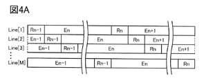
- FIG. 4A is a diagram illustrating a rolling shutter system.
- FIG. 4B is a diagram illustrating the global shutter system.
- FIG. 5 is a diagram illustrating a read circuit.
- FIG. 6 is a timing chart for explaining the operation of the image pickup apparatus.
- FIG. 7 is a block diagram illustrating an imaging device.
- 8A to 8C are diagrams illustrating a light emitting device and a photoelectric conversion device.
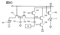
- 9A to 9C are diagrams illustrating a pixel circuit.
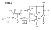
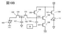
- 10A to 10C are diagrams illustrating a pixel circuit.
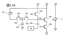
- 11A to 11C are diagrams illustrating a pixel circuit.
- 12A to 12C are diagrams illustrating a pixel circuit.
- 13A and 13B are diagrams illustrating a pixel circuit.
- 14A to 14C are diagrams illustrating the configuration of pixels, the configuration of photoelectric conversion devices, and the configuration of light emitting devices of an imaging device.
- FIG. 15 is a diagram illustrating a pixel configuration of an image pickup device.
- 16A to 16D are diagrams illustrating transistors.
- 17A1, 17A2, 17B1, and 17B2 are diagrams illustrating electronic devices.
- 18A and 18B are diagrams illustrating electronic devices.
- the element may be composed of a plurality of elements.
- a plurality of transistors which operate as switches may be connected in series or in parallel.
- a capacitor also referred to as a capacitor
- a capacitor may be divided and placed at a plurality of positions.
- one conductor may have a plurality of functions such as wiring, an electrode, and a terminal in some cases, and in this specification, a plurality of names may be used for the same element. Further, even when the elements are illustrated as directly connected on the circuit diagram, the elements may actually be connected through a plurality of conductors, and In the book, such a structure is included in the category of direct connection.
- One embodiment of the present invention is an imaging device including a light emitting device and a photoelectric conversion device in a pixel. The light emitted from the light emitting device and reflected by the subject is received by the photoelectric conversion device. Since an EL element is used for the light emitting device, a thin imaging device with a light source can be configured.
- a configuration in which a plurality of EL elements having different emission wavelengths are provided and a configuration in which a plurality of photoelectric conversion devices having different reception wavelengths are provided can also be adopted. Therefore, it is possible to obtain information about the subject for a plurality of wavelengths.
- the imaging device also has a function of outputting third data obtained by multiplying the first data acquired by the pixel by the second data (weight).
- third data obtained by multiplying the first data acquired by the pixel by the second data (weight).
- an element that emits infrared light as a light emitting device, it can be used for applications such as biometric authentication, measurement of physical activity, failure analysis of industrial products, and selection of agricultural products. Further, by using a pixel circuit capable of capturing an image by the global shutter method, an image without distortion can be obtained even for a moving subject.
- FIG. 1 is a block diagram illustrating an imaging device of one embodiment of the present invention.
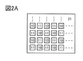
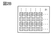
- the imaging device includes a pixel array 21 having pixels arranged in a matrix, a circuit 22 (row driver) having a function of selecting a row of the pixel array 21, and a circuit 23 having a function of reading data from the pixel circuit 10. And a circuit 28 for supplying a power supply potential.
- a pixel circuit 10 and a light emitting device 11 are provided in the pixel.
- the circuit 23 is a readout circuit and includes a circuit 24 (first CDS circuit) for performing correlated double sampling processing on the output data of the pixel circuit 10 and a correlated double sampling processing for the output data of the circuit 24.
- a circuit 25 (second CDS circuit) for performing the above, a circuit 26 (A / D conversion circuit or the like) having a function of converting analog data output from the circuit 25 into digital data, and a pixel array 21 for reading data.
- the circuit 23 may be provided with a current source circuit or the like.
- the pixel circuit 10 and the light emitting device 11 may not overlap.
- the pixel circuits 10 and the light emitting devices 11 may be alternately arranged at regular intervals.
- the pixel circuits 10 and the light emitting devices 11 may be alternately arranged in each row.
- the light emitting device 11 may be extended in one direction as indicated by a broken line.
- the light emitting device 11 may be arranged between two adjacent pixel circuits 10.
- the light emitting device 11 is arranged so as to have a region overlapping with the wiring connected to the pixel circuit 10.
- 2A to 2C show the same number of light emitting devices 11 as the pixel circuits 10, the number of light emitting devices 11 may be different from that of the pixel circuits 10.
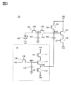
- FIG. 3 is a circuit diagram illustrating the pixel circuit 10 that can be used for the imaging device of one embodiment of the present invention.
- the pixel circuit 10 can include a photoelectric conversion device 101, a transistor 102, a transistor 103, a transistor 104, a transistor 105, a transistor 106, a capacitor 107, a capacitor 108, and a memory circuit 30. Note that the capacitor 107 may not be provided.
- One electrode (cathode) of the photoelectric conversion device 101 is electrically connected to one of a source and a drain of the transistor 102.
- the other of the source and the drain of the transistor 102 is electrically connected to one electrode of the capacitor 107.
- One electrode of the capacitor 107 is electrically connected to one of a source and a drain of the transistor 103.
- the other of the source and the drain of the transistor 103 is electrically connected to one of the source and the drain of the transistor 104.
- One of a source and a drain of the transistor 104 is electrically connected to one electrode of the capacitor 108.
- One electrode of the capacitor 108 is electrically connected to the gate of the transistor 105.
- One of a source and a drain of the transistor 105 is electrically connected to one of a source and a drain of the transistor 106.
- the other electrode of the capacitor 108 is electrically connected to the memory circuit 30.
- the memory circuit 30 can include the transistor 110, the transistor 111, the transistor 112, the transistor 113, and the capacitor 114.
- One of a source and a drain of the transistor 110 is electrically connected to one electrode of the capacitor 114.
- One electrode of the capacitor 114 is electrically connected to the gate of the transistor 112.
- One of a source and a drain of the transistor 112 is electrically connected to one of a source and a drain of the transistor 111.
- the other of the source and the drain of the transistor 112 is electrically connected to one of the source and the drain of the transistor 113.
- One of a source and a drain of the transistor 113 is electrically connected to the other electrode of the capacitor 108.
- a wiring connecting the other of the source and the drain of the transistor 102, one electrode of the capacitor 107, and one of the source and the drain of the transistor 103 is referred to as a node FD1.
- a wiring that connects the other of the source and the drain of the transistor 103, the one of the source and the drain of the transistor 104, the one electrode of the capacitor 108, and the gate of the transistor 105 is referred to as a node FD2.
- the node FD1 can function as a charge storage unit.
- the node FD2 can function as a charge detection unit.
- a wiring connecting one of the source and the drain of the transistor 110, one electrode of the capacitor 114, and the gate of the transistor 112 is referred to as a node NW1.
- a wiring connecting the other of the source and the drain of the transistor 112, the one of the source and the drain of the transistor 113, and the other electrode of the capacitor 108 is referred to as a node NW2.
- the node NW1 can function as a data holding node.
- the node NW2 can function as a data read node.
- the other electrode (anode) of the photoelectric conversion device 101 is electrically connected to the wiring 121.
- the gate of the transistor 102 is electrically connected to the wiring 124.
- the gate of the transistor 103 is electrically connected to the wiring 125.
- the other of the source and the drain of the transistor 104 and the other of the source and the drain of the transistor 105 are electrically connected to the wiring 122.
- the gate of the transistor 104 is electrically connected to the wiring 126.
- the gate of the transistor 106 is electrically connected to the wiring 127.
- the other of the source and the drain of the transistor 106 is electrically connected to the wiring 123.
- the other electrode of the capacitor 107 is electrically connected to a reference potential line such as a GND wiring, for example.
- the other of the source and the drain of the transistor 110 is electrically connected to the wiring 133.
- the other of the source and the drain of the transistor 111 is electrically connected to the wiring 134.
- the other of the source and the drain of the transistor 113 is electrically connected to the wiring 135.
- the other electrode of the capacitor 114 is electrically connected to a reference potential line such as a GND wiring.
- the wirings 124, 125, 126, 127, 136, 137, and 138 can function as signal lines which control conduction of each transistor.
- the wirings 121 and 122 can have a function as power supply lines.
- the cathode side of the photoelectric conversion device 101 is electrically connected to the transistor 102, and the node FD1 and the node FD2 are reset to a high potential to operate, so that the wiring 122 has a high potential ( The potential is higher than that of the wiring 121).
- the transistor 112 and the transistor 113 operate as a source follower, and the potential of the node NW1 can be read to the node NW2.
- the wirings 134 and 135 can function as a power supply line for operating the transistor 112, and the wiring 134 has a high potential (a potential higher than that of the wiring 135).
- the wiring 123 can function as an output line.
- the wiring 133 in the memory circuit can function as a signal line for writing data (weight).
- a photodiode can be used as the photoelectric conversion device 101.
- imaging using infrared rays is performed. Therefore, the photoelectric conversion device 101 uses a photodiode capable of photoelectrically converting at least light in the infrared region.
- a photodiode having an organic photoconductive film in the photoelectric conversion layer can be used.
- the organic photoconductive film is a thin film and can be bent if the supporting substrate is flexible. Therefore, it is suitable for forming a flexible imaging device. Further, it is easy to increase the size of the image pickup device.
- a photoconductor having an organic photoconductive film may be used as the photoelectric conversion device 101.
- a pn junction photodiode using single crystal silicon for a photoelectric conversion portion a pin photodiode using polycrystalline silicon, or microcrystalline silicon for a photoelectric conversion layer can be used.
- a photodiode having a material capable of photoelectrically converting light in the infrared region such as a compound semiconductor may be used.
- an infrared transmission filter (a filter that blocks visible light) is preferably provided between the photoelectric conversion device 101 and the subject.
- the transistor 102 has a function of controlling the potential of the node FD1.
- the transistor 103 has a function of controlling the potential of the node FD2.
- the transistor 104 has a function of resetting the potentials of the node FD1 and the node FD2.
- the transistor 105 functions as a source follower circuit and can output the potential of the node FD2 as image data to the wiring 123.
- the transistor 106 has a function of selecting a pixel which outputs image data.
- a transistor including a metal oxide in a channel formation region (hereinafter referred to as an OS transistor) is preferably used.
- the OS transistor has a characteristic of extremely low off-state current.
- FIG. 4A is a schematic diagram of the rolling shutter system operation method
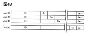
- FIG. 4B is a schematic diagram of the global shutter system.
- En represents the exposure (accumulation operation) of the nth column (n is a natural number)
- Rn represents the read operation of the nth column.
- 4A and 4B show the operation from the first line (Line [1]) to the Mth line (Line [M]) (M is a natural number).
- the rolling shutter method is an operation method of sequentially performing exposure and reading of data, and is a method of overlapping a reading period of a certain row and an exposure period of another row. Since the reading operation is performed immediately after the exposure, imaging can be performed even with a circuit configuration in which the data retention period is relatively short. However, since an image of one frame is composed of data that does not have image capturing simultaneity, the image is distorted when capturing a moving object.
- the global shutter method is an operation method in which all pixels are exposed at the same time, data is held in each pixel, and data is read row by row. Therefore, it is possible to obtain an image without distortion even when capturing a moving object.
- a transistor having a relatively high off current such as a transistor using Si in a channel formation region (hereinafter referred to as a Si transistor)
- a rolling shutter method is used because a data potential easily flows out from a charge storage portion.
- Si transistors it is necessary to separately provide a memory circuit and the like, and more complicated operations must be performed at high speed.
- the OS transistor is used in the pixel circuit, the data potential hardly flows out from the charge storage portion, so that the global shutter system can be easily realized.
- OS transistors are also preferably used for the transistors 110, 111, 112, and 113 in the memory circuit 30.
- the OS transistor By using the OS transistor as the transistor 110, the potential of the node NW1 can be held extremely long. Therefore, if the data is the same, the frequency of writing to the node NW1 can be reduced.
- the potential of the node NW2 can be held extremely long. Since the potential of the node FD2 is stable because the potential of the node NW2 can be held for a long period of time, reliable data can be read from the pixel circuit 10.
- an OS transistor may be applied to other transistors included in the pixel circuit 10.
- the OS transistor and the Si transistor may be applied in any combination.
- all the transistors may be OS transistors.
- all transistors may be Si transistors. Examples of the Si transistor include a transistor having amorphous silicon, a transistor having crystalline silicon (typically, low temperature polysilicon, single crystal silicon, or the like).
- An EL element can be used for the light emitting device 11.
- An element that emits infrared light can be used as the EL element.
- an EL element that emits near-infrared light having a peak at a wavelength of 700 nm to 2500 nm is preferable.
- the position of veins can be detected by receiving reflected light from the palm, fingers, etc. and imaging it. The action can be used as biometrics.
- the received light amounts of the light having a wavelength with large absorption of reduced hemoglobin and the light having a wavelength with large absorption of oxyhemoglobin eg, 940 nm
- the function can be used for analysis of brain function and the like.
- the blood oxygen concentration can also be measured by comparing the amount of received light with the wavelength absorbed by reduced hemoglobin and the amount of received light with the wavelength absorbed by oxyhemoglobin. If glucose in the blood is the target of infrared light absorption, the blood glucose level can also be measured.
- non-destructive inspection such as foreign substance inspection in food and defect analysis of industrial products can be performed by using near infrared light having an appropriate wavelength. Further, by combining with the global shutter system, it is possible to perform highly accurate sensing even if the subject moves.
- the imaging device In the analysis of brain function, it is necessary to bring a relatively large-area imaging device (sensor) into close contact with the head. Therefore, the imaging device must be flexible or have a curved surface conforming to the shape of the head. It is preferable that an imaging device having a property is formed. In order to give flexibility to the image pickup device, first, a method of completing the image pickup device on a hard substrate and transposing it on a soft substrate is adopted.
- the process temperature of the transistor or the like may be limited. Therefore, the electrical characteristics and reliability of the transistor may be deteriorated. Laser irradiation is required to form a transistor including polycrystalline silicon, and peeling failure may occur due to laser damage to the buffer layer and peripheral members.
- the OS transistor when forming a flexible imaging device, it is preferable to use an OS transistor. Since the OS transistor can be formed at a relatively low temperature and a laser irradiation step is unnecessary, it can be said that the OS transistor does not have the above problem and is suitable for a flexible imaging device.
- an EL element as the light emitting device 11, it is possible to realize a thin imaging device with a light source, facilitate mounting on various devices, and improve portability.
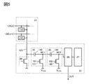
- FIG. 5 is a diagram illustrating a circuit 23 connected to a specific column of the pixel array 21.
- the current source circuit 29 is electrically connected to the wiring 123 from which data is output from the pixel circuit 10.
- a circuit 24 first CDS circuit
- a circuit 25 second CDS circuit
- a circuit 26 A / D conversion circuit
- a circuit 27 shift register
- the circuit 24 can have a structure including the transistor 141 and the capacitor 143. Further, the circuit 25 can have a structure including the transistor 142 and the capacitor 144.
- One electrode of the capacitor 143 is electrically connected to the wiring 123.
- the other electrode of the capacitor 143 is electrically connected to one of a source and a drain of the transistor 141.
- One of a source and a drain of the transistor 141 is electrically connected to one electrode of the capacitor 144.
- the other electrode of the capacitor 144 is electrically connected to one of a source and a drain of the transistor 142.
- One of a source and a drain of the transistor 142 is electrically connected to the circuit 26.
- the circuit 26 is electrically connected to the circuit 27.
- the circuit 26 can include, for example, a comparator, a counter, an output portion (OUT), and the like.
- a wiring connecting the other electrode of the capacitor 143, one of the source and the drain of the transistor 141, and one electrode of the capacitor 144 is referred to as a node NC1.
- a wiring connecting the other electrode of the capacitor 144, one of the source and the drain of the transistor 142, and the circuit 26 is a node NC2.
- the other of the source and the drain of the transistor 141 and the other of the source and the drain of the transistor 142 are electrically connected to a wiring which can supply a reference potential (V CDS ).
- the imaging device of one embodiment of the present invention can output the third data obtained by multiplying the first data acquired by the pixel by the second data (weight).
- the third data can be generated using the pixel circuit 10, the circuit 24, and the circuit 25, and unnecessary components are removed. Next, the description will be given.
- the third data includes data without exposure (D r ) output from the pixel circuit 10, data (D r + w ) obtained by weighting data without exposure, data with exposure (D r + x ), and data with exposure. It is generated using weighted data (D r + x + w ).
- the amount of change (difference) in the presence or absence of weight is calculated for each of the case with no exposure and the case with exposure. Specifically, formula (2) -formula (1) and formula (4) -formula (3) are calculated.
- the operation of outputting the data corresponding to the equations (1) to (4) can be performed by the pixel circuit 10.
- the calculation operation of the data corresponding to the equations (5) and (6) can be performed mainly by the circuit 24.
- the operation of calculating the data corresponding to Expression (7) can be performed mainly by the circuit 25.
- the potential of the wiring 124 is “H”
- the potential of the wiring 125 is “H”
- the potential of the wiring 126 is “H”
- the potential of the wiring 127 is “L”
- the potential of the wiring 136 is “H”
- the wiring is
- the potential of 137 is “L”
- the potential of the wiring 138 is “H”
- the potential of the wiring 151 is “L”
- the potential of the wiring 152 is “L”
- the transistors 102, 103, and 104 are conductive and the node FD1 and
- the potential “H” (r: reset potential) of the wiring 122 is supplied to the node FD2 (reset operation).
- the transistor 113 is turned on and the potential “L” of the wiring 135 is written to the node NW2. At this time, "r-L” is held in the capacitor 108. Further, the transistor 110 is turned on, and the potential “w” supplied from the wiring 133 is written to the node NW1.
- the writing of the weight to the node NW1 is not limited to the period T1 and may be performed before the weight is read to the node NW2.
- the potential of the wiring 124 is “H”
- the potential of the wiring 125 is “L”
- the potential of the wiring 126 is “L”
- the potential of the wiring 127 is “L”
- the potential of the wiring 136 is “L”
- the wiring is
- the potential of 137 is “L”
- the potential of the wiring 138 is “H”
- the potential of the wiring 151 is “L”
- the potential of the wiring 152 is “L”
- the reset potential "r” is held.
- the potential of the node FD1 changes by the potential “x” of the exposure amount according to the operation of the photoelectric conversion device 101 and becomes “r + x” (accumulation operation).
- the potential of the wiring 124 is “L”
- the potential of the wiring 125 is “L”
- the potential of the wiring 126 is “L”
- the potential of the wiring 127 is “L”
- the potential of the wiring 136 is “L”
- the wiring is
- the potential of 137 is “L”
- the potential of the wiring 138 is “H”
- the potential of the wiring 151 is “L”
- the potential of the wiring 152 is “L”
- the transistor 102 is non-conductive and the potential of the node FD1 is fixed. And then retained.
- the transistor 110 is turned off and the potential of the node NW1 is held.
- the potential of the wiring 124 is “L”
- the potential of the wiring 125 is “L”
- the potential of the wiring 126 is “L”
- the potential of the wiring 127 is “H”
- the potential of the wiring 136 is “L”
- the wiring is
- the potential of 137 is “L”
- the potential of the wiring 138 is “H”
- the potential of the wiring 151 is “H”
- the potential of the wiring 152 is “H”
- a current proportional to the function (r ⁇ V th ) 2 including the potential “r” of the node FD2 flows through the wiring 123 (read operation 1). The operation corresponds to the above-mentioned formula (1).
- the transistor 141 of the circuit 24 and the transistor 142 of the circuit 25 are rendered conductive, and the reference potential “V CDS ” is written to the nodes NC1 and NC2, respectively.
- the potential of the wiring 124 is “L”
- the potential of the wiring 125 is “L”
- the potential of the wiring 126 is “L”
- the potential of the wiring 127 is “H”
- the potential of the wiring 136 is “L”
- the wiring is
- the potential of 137 is “H”
- the potential of the wiring 138 is “L”
- the potential of the wiring 151 is “L”
- the potential of the wiring 152 is “H”
- the transistor 111 is conductive and the transistor 113 is turned on in the memory circuit 30. It becomes non-conductive, and the potential "w" of the node NW1 is read to the node NW2 by the source follower operation of the transistor 112.
- the potential of the node FD2 becomes “r ⁇ L + w” due to the capacitive coupling of the capacitor 108.
- the potential of the node FD2 becomes “r + w”. Therefore, due to the source follower operation of the transistor 105, a current proportional to a function (r + w ⁇ V th ) 2 including “r + w” flows in the wiring 123. The operation corresponds to the above-mentioned formula (2).
- the transistor 141 becomes non-conductive.
- the operation corresponds to the above-mentioned equation (5).
- the potential of the wiring 124 is “L”
- the potential of the wiring 125 is “H”
- the potential of the wiring 126 is “L”
- the potential of the wiring 127 is “H”
- the potential of the wiring 136 is “L”
- the wiring is
- the potential of 137 is “L”
- the potential of the wiring 138 is “H”
- the potential of the wiring 151 is “H”
- the potential of the wiring 152 is “L”
- the transistor 103 is turned on and the potential of the node FD1 is applied to the node FD2.
- the potential of "r + w" is read.
- the transistor 111 is turned off and the transistor 113 is turned on, so that the potential “L” of the wiring 135 is written to the node NW2. At this time, “r + x ⁇ L” is held in the capacitor 108.
- the potential of the wiring 124 is “L”
- the potential of the wiring 125 is “H”
- the potential of the wiring 126 is “L”
- the potential of the wiring 127 is “H”
- the potential of the wiring 136 is “L”
- the wiring is
- the potential of 137 is “H”
- the potential of the wiring 138 is “L”
- the potential of the wiring 151 is “L”
- the potential of the wiring 152 is “L”
- the transistor 111 is on and the transistor 113 is on in the memory circuit 30. It becomes non-conductive, and the potential "w" of the node NW1 is read to the node NW2 by the source follower operation of the transistor 112.
- the potential of the node FD2 becomes “r + x ⁇ L + w” due to the capacitive coupling of the capacitor 108.
- the potential of the node FD2 becomes “r + x + w”. Therefore, due to the source follower operation of the transistor 105, a current proportional to a function (r + x + w ⁇ V th ) 2 including “r + x + w” flows through the wiring 123.
- the operation corresponds to the above-mentioned formula (4).
- the transistor 141 becomes non-conductive.
- the operation corresponds to the above-mentioned equation (6).
- the transistor 142 of the circuit 25 becomes non-conductive.
- the operation corresponds to the above-mentioned equation (7). Therefore, information on the product of the exposure data (x) and the weight (w) can be extracted from the circuit 25.
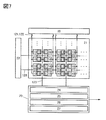
- the imaging device of one embodiment of the present invention may have the structure of the block diagram illustrated in FIG. 7.
- the image pickup apparatus shown in FIG. 7 is different from the image pickup apparatus shown in FIG. 1 in that a plurality of pixel circuits 10 share a read gate line (wiring 128) and an output line (wiring 123).
- FIG. 7 shows an example in which wirings such as output lines are shared by four pixels, the number is two or more and is not limited as long as the total number of pixels can be equally divided.
- the imaging device can also be operated according to the timing chart shown in FIG. 6 and the description thereof. The derived functions are shown below.
- n is an integer of 1 to 4.
- the current read to the wiring 123 at time T4 is proportional to ⁇ n (r ⁇ V th ) 2 .
- the current read to the wiring 123 at time T5 is proportional to ⁇ n (r + w n ⁇ V th ) 2 .
- the current read to the wiring 123 at time T6 is proportional to ⁇ n (r + x n ⁇ V th ) 2 .
- the current read out to the wiring 123 at time T7 is proportional to ⁇ n (r + x n + w n ⁇ V th ) 2 .
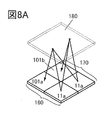
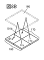
- 8A to 8C are diagrams illustrating the first pixel 160, the second pixel 170, and the subject 180.
- the first pixel 160 and the second pixel 170 can be applied to the pixels included in the pixel array 21.
- the size of one side is 1 mm or less, preferably 100 ⁇ m or less.
- FIG. 8A shows a configuration in which the first pixel 160 has the photoelectric conversion device 101a, the second pixel 170 has the photoelectric conversion device 101b, and both pixels have the light emitting device 11a.
- the light emitted from the light emitting device 11a is partially absorbed by the subject 180, and the light reflected by the subject 180 is received by each pixel.
- the arrow shown in the figure has shown a part of path
- the light emitting device 11a includes an EL element that emits light having a broad wavelength distribution including the wavelengths A and B. Can be used.
- the absorption edge wavelength of the photoelectric conversion device 101a can be shorter than the wavelength B, and the absorption edge wavelength of the photoelectric conversion device 101b can be set to the wavelength B or more.
- a photodiode in which a semiconductor material having an absorption edge wavelength near wavelength A is used for a photoelectric conversion layer can be used.
- a photodiode in which a semiconductor material having an absorption edge wavelength in the vicinity of the wavelength B is used for the photoelectric conversion layer can be used.
- the photoelectric conversion layer may be formed of a semiconductor material having sensitivity in a wavelength range including wavelength A and wavelength B in both the photoelectric conversion devices 101a and 101b.
- an optical filter that transmits the wavelength A and its vicinity may be provided on the photoelectric conversion device 101a, and an optical filter that transmits the wavelength B and its vicinity may be provided on the photoelectric conversion device 101b.
- the first pixel 160 can obtain information on light near the wavelength A and light having a shorter wavelength.
- the second pixel 170 can obtain information on light near the wavelength B and light having a shorter wavelength. That is, if the difference between the information obtained by the first pixel 160 and the information obtained by the second pixel 170 is taken, the data of the wavelength B and its vicinity can be extracted.
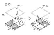
- FIG. 8B shows a configuration in which the first pixel 160 includes the photoelectric conversion device 101a and the light emitting device 11b, and the second pixel 170 includes the photoelectric conversion device 101b and the light emitting device 11b.
- An EL element that emits light having a peak at the wavelength A can be used for the light emitting device 11b.
- An EL element that emits light having a peak at the wavelength B can be used for the light emitting device 11c.
- the wavelength distribution of the light source is not broad, it is possible to directly obtain information on light having a peak at wavelength A by the photoelectric conversion device 101a.
- information on light having a peak at the wavelength B can be directly obtained by the photoelectric conversion device 101b.
- FIG. 8C shows a configuration in which the first pixel 160 has the light emitting device 11b, the second pixel 170 has the light emitting device 11c, and both pixels have the photoelectric conversion device 101b.
- the absorption edge wavelength of the photoelectric conversion device 101b is set to the wavelength B or more, and the first pixel 160 and the second pixel 170 are operated with a time difference (T1, T2).
- T1 the information of the light having the peak at the wavelength B can be directly obtained by the photoelectric conversion device 101b included in the pixel 170.
- T2 information on light having a peak at the wavelength A can be directly obtained by the photoelectric conversion device 101b included in the pixel 160.
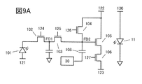
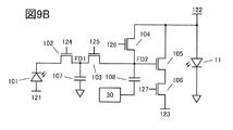
- FIG. 9A is a circuit diagram illustrating a pixel circuit 10 and a light emitting device 11 which can be provided in a pixel of an imaging device of one embodiment of the present invention.
- the pixel circuit 10 has the same configuration as that shown in FIG.
- the input potential to the light emitting device 11 and the light emission timing can be controlled independently.
- One electrode of the light emitting device 11 is electrically connected to the wiring 130.
- the wiring 130 has a function of supplying a forward bias to the light emitting device 11 to supply a potential for emitting light.
- the other electrode of the light emitting device 11 is electrically connected to a reference potential line such as a GND wiring.
- FIG. 9B shows a configuration in which one electrode of the light emitting device 11 is electrically connected to the wiring 122.
- the reset potentials of the nodes FD1 and FD2 the power supply potential supplied to the transistor 105, and the input potential of the light-emitting device 11 can be made common, this structure can be used.
- the transistor 109 may be added to the structure of FIG. 9B.
- One of a source and a drain of the transistor 109 is electrically connected to one electrode of the light emitting device 11.
- the other of the source and the drain of the transistor 109 is electrically connected to the wiring 122.
- the gate of the transistor 109 is electrically connected to the wiring 124.
- the resistance element 115 may be electrically connected.
- the resistance element 115 acts as a current limiting resistance, can limit the current flowing through the light emitting device 11, and can enhance the reliability of the light emitting device 11.
- an appropriate value may be selected according to the electrical characteristics of the light emitting device 11.
- the transistor 109 shown in FIG. 9C may be operated as a substitute for the resistance element 115.
- the gate of the transistor 109 is electrically connected to the wiring 131. Therefore, by changing the potential of the wiring 131, the illuminance of the light emitting device 11 and the timing of light emission can be arbitrarily controlled, and power consumption can be suppressed.
- the other of the source and the drain of the transistor 109 is electrically connected to the wiring 130, and the gate of the transistor 109 is electrically connected to the wiring 124. It may be configured.
- the input potential to the light emitting device 11 is controlled by the wiring 130, and the timing of light emission is controlled by the wiring 124.
- FIGS. 10A to 10C show the structure in which the cathode of the photoelectric conversion device 101 is electrically connected to the transistor 102.
- the anode of the photoelectric conversion device 101 may be electrically connected to the transistor 102.
- one electrode of the photoelectric conversion device 101 is electrically connected to the wiring 122, and the other electrode of the photoelectric conversion device 101 is a source or a drain of the transistor 102. It is electrically connected to one side. The other of the source and the drain of the transistor 104 is electrically connected to the wiring 132.
- the wiring 132 can function as a power supply line or a reset potential supply line.
- the node FD1 and the node FD2 are reset to a low potential to operate, so that the wiring 132 has a low potential (a potential lower than that of the wiring 122). .
- FIGS. 9A to 9C and FIGS. 10A to 10C can be referred to for the description of the connection mode between the light-emitting device 11 and the peripheral elements thereof, which are illustrated in FIGS. 11A to 11C and FIGS. 12A to 12C.
- the OS transistor included in the imaging device may have a structure in which a back gate is provided.
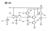
- FIG. 13A shows a configuration in which the back gate is electrically connected to the front gate, which has the effect of increasing the on-current.
- FIG. 13B shows a structure in which the back gate is electrically connected to a wiring which can supply a constant potential, and the threshold voltage of the transistor can be controlled.
- the pixel circuit 13A and 13B may be combined so that each transistor can perform an appropriate operation.
- the pixel circuit may include a transistor in which a back gate is not provided. Note that the structure in which the back gate is provided in the transistor can be applied to all the pixel circuits and peripheral circuits described in this embodiment.
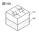
- FIG. 14A illustrates a structure of a pixel included in the imaging device.
- the pixel can have a stacked-layer structure of a layer 510 including the light-emitting device 11 and the photoelectric conversion device 101, and a layer 520 including a transistor or the like included in the pixel circuit 10.
- Each layer has a supporting substrate.
- a light-emitting device (EL element) utilizing electroluminescence can be used as the light-emitting device 11 included in the layer 510.
- the EL element has a layer containing a light-emitting compound (EL layer) between a pair of electrodes.
- EL layer a light-emitting compound
- EL elements are distinguished depending on whether a light emitting material is an organic compound or an inorganic compound. Generally, the former is called an organic EL element and the latter is called an inorganic EL element.
- the organic EL element In the organic EL element, electrons are injected from one electrode and holes are injected into the EL layer from the other electrode by applying a voltage. When the carriers (electrons and holes) are recombined, the light-emitting organic compound forms an excited state and emits light when the excited state returns to the ground state. Due to such a mechanism, such a light emitting device is called a current excitation type light emitting device.
- the EL layer can be formed by an evaporation method (including a vacuum evaporation method), a transfer method, a printing method, an inkjet method, a coating method, or the like.
- the inorganic EL element is classified into a dispersion type inorganic EL element and a thin film type inorganic EL element depending on the element structure.
- the dispersion-type inorganic EL device has a light-emitting layer in which particles of a light-emitting material are dispersed in a binder, and the light emission mechanism is donor-acceptor recombination light emission that utilizes a donor level and an acceptor level.
- the thin film type inorganic EL device has a structure in which a light emitting layer is sandwiched by dielectric layers and further sandwiched by electrodes, and the light emission mechanism is localized type light emission utilizing the core electron transition of metal ions.
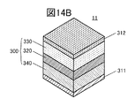
- FIG. 14B shows the configuration of the light emitting device 11 (EL element).
- the EL layer 300 can be formed using a plurality of layers such as a layer 330, a light emitting layer 320, and a layer 340.
- the layer 330 can include, for example, a layer containing a substance having a high electron-injection property (electron injection layer), a layer containing a substance having a high electron-transport property (electron transport layer), and the like.
- the light emitting layer 320 has, for example, a light emitting compound.
- the layer 340 can include, for example, a layer including a substance having a high hole-injection property (a hole-injection layer) and a layer including a substance having a high hole-transport property (a hole-transport layer).
- the EL layer 300 provided between the electrode 311 and the electrode 312 can function as a single light emitting unit. Note that a plurality of light emitting layers may be provided between the layers 330 and 340. Note that the light emitting direction is determined by using a light-transmitting conductive film for either one of the electrode 311 and the electrode 312.
- the light emitting device 11 can emit light of various wavelengths depending on the material forming the EL layer 300.
- a material that emits light having a peak in near-infrared light (wavelength 720 to 2500 nm) is used as a material forming the EL layer 300.
- a material that emits light having a wavelength of 720 nm, 760 nm, 850 nm, 900 nm, 940 nm or in the vicinity of these wavelengths may be used depending on the application.
- the light-emitting material of the EL layer 300 (also referred to as a guest material or a dopant material) include an organometallic iridium complex which emits near-infrared light.
- the organometallic iridium complex preferably has a dimethylphenyl skeleton and a quinoxaline skeleton.
- organometallic iridium complex typically, bis ⁇ 4,6-dimethyl-2- [3- (3,5-dimethylphenyl) -2-quinoxalinyl- ⁇ N] phenyl- ⁇ C ⁇ (2, 2 ′, 6,6′-Tetramethyl-3,5-heptanedionato- ⁇ 2 O, O ′) iridium (III) (abbreviation: Ir (dmdpq) 2 (dpm)) or the like can be used.
- Ir (dmdpq) 2 (dpm) iridium
- an imaging element with high quantum efficiency or light emission efficiency can be provided.
- Examples of the substance used to bring the organometallic iridium complex into a dispersed state include aryls such as 2,3-bis (4-diphenylaminophenyl) quinoxaline (abbreviation: TPAQn) and NPB.
- aryls such as 2,3-bis (4-diphenylaminophenyl) quinoxaline (abbreviation: TPAQn) and NPB.
- carbazole derivatives such as CBP, 4,4 ′, 4 ′′ -tris (carbazol-9-yl) triphenylamine (abbreviation: TCTA), and bis [2- (2′-hydroxy) Phenyl) pyridinato] zinc (abbreviation: Znpp 2 ), bis [2- (2-hydroxyphenyl) benzoxazolato] zinc (abbreviation: Zn (BOX) 2 ), bis (2-methyl-8-quinolinolato) (4 -Phenylphenolato) aluminum (III) (abbreviation: BAlq), tris (8-quinolinolato) aluminum (III (Abbreviation: Alq 3) metal complexes, and the like are preferable. Further, a polymer compound such as PVK can also be used.
- the material (host material) used to bring the organometallic iridium complex into a dispersed state is N- (1,1′-biphenyl-4-yl) -N- [4- (9-phenyl-9H- Carbazol-3-yl) phenyl] -9,9-dimethyl-9H-fluoren-2-amine (abbreviation: PCBBiF) is preferably used.
- near-infrared phosphorescence with high emission efficiency can be obtained from the EL layer 300 by forming the light-emitting layer 320 containing the above-described organometallic iridium complex (guest material) and the above-mentioned host material.
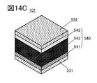
- the photoelectric conversion device 101 included in the layer 510 a photodiode, a photoconductor, or the like can be used.
- the photoelectric conversion device 101 can be a stack of a layer 531, a layer 540, and a layer 532 as illustrated in FIG. 14C.
- the photoelectric conversion device 101 illustrated in FIG. 14C is an example of an organic photoconductive film, and the layers 531 and 532 correspond to electrodes, and one of them has a light-transmitting property, so that light can be introduced into the photoelectric conversion portion.
- the layer 540 corresponds to a photoelectric conversion portion and includes a layer 541, a layer 542, and a layer 542.
- One of the layers 541 and 543 of the photoelectric conversion portion can be a hole transport layer and the other can be an electron transport layer. Further, the layer 542 can be a photoelectric conversion layer.
- the hole transport layer for example, molybdenum oxide or the like can be used.
- the electron transport layer for example, fullerenes such as C60 and C70, or derivatives thereof can be used.
- a mixed layer (bulk heterojunction structure) of an n-type organic semiconductor and a p-type organic semiconductor can be used.
- materials for the photoelectric conversion layer include organic semiconductor materials such as copper (II) phthalocyanine (Copper (II) phthalocyanine; CuPc) and tetraphenyldibenzoperifuranthene (DBP).
- a pn junction photodiode formed using single crystal silicon a pin junction photodiode formed using a thin film of single crystal silicon, microcrystalline silicon, polycrystalline silicon, or the like is used. May be.
- Single crystal silicon, microcrystalline silicon, and polycrystalline silicon have sensitivity to infrared light and are suitable for detecting infrared light.
- the layer 520 is mainly provided with elements such as a transistor included in the pixel circuit 10. Further, part or all of the transistors included in the peripheral circuit described in Embodiment 1 may be included. An OS transistor is preferably used as the transistor.
- a metal oxide having an energy gap of 2 eV or more, preferably 2.5 eV or more, more preferably 3 eV or more can be used.
- it is an oxide semiconductor containing indium, and for example, CAAC-OS or CAC-OS described later can be used.
- CAAC-OS is suitable for a transistor and the like in which the atoms forming a crystal are stable and reliability is important. Further, since the CAC-OS exhibits high mobility characteristics, it is suitable for a transistor or the like which drives at high speed.
- the OS transistor Since the OS transistor has a large energy gap in the semiconductor layer, it exhibits extremely low off-current characteristics of several yA / ⁇ m (current value per 1 ⁇ m of channel width). Further, the OS transistor has characteristics different from those of the Si transistor such that impact ionization, avalanche breakdown, short channel effect, and the like do not occur, and a high breakdown voltage and highly reliable circuit can be formed. Further, variations in electrical characteristics due to non-uniformity of crystallinity, which is a problem in Si transistors, are less likely to occur in OS transistors.
- the semiconductor layer included in the OS transistor is an In-M including, for example, indium, zinc, and M (one or more of metals such as aluminum, titanium, gallium, germanium, yttrium, zirconium, lanthanum, cerium, tin, neodymium, or hafnium). It can be a film represented by a —Zn-based oxide.
- the In-M-Zn-based oxide can be typically formed by a sputtering method. Alternatively, it may be formed by using an ALD (Atomic layer deposition) method.
- the atomic ratio of the metal elements of the sputtering target used for forming the In-M-Zn-based oxide by a sputtering method preferably satisfies In? M and Zn? M.
- the atomic ratio of the semiconductor layers to be formed includes a fluctuation of ⁇ 40% in the atomic ratio of the metal elements contained in the sputtering target.
- the semiconductor layer has a carrier density of 1 ⁇ 10 17 / cm 3 or less, preferably 1 ⁇ 10 15 / cm 3 or less, more preferably 1 ⁇ 10 13 / cm 3 or less, and more preferably 1 ⁇ 10 11 / cm 3. 3 or less, more preferably less than 1 ⁇ 10 10 / cm 3 , and 1 ⁇ 10 ⁇ 9 / cm 3 or more of an oxide semiconductor can be used.
- Such an oxide semiconductor is referred to as a high-purity intrinsic or substantially high-purity intrinsic oxide semiconductor. It can be said that the oxide semiconductor has a low density of defect states and stable characteristics.
- the composition is not limited to these, and a material having an appropriate composition may be used depending on required semiconductor characteristics and electric characteristics (field effect mobility, threshold voltage, or the like) of the transistor. Further, in order to obtain the required semiconductor characteristics of the transistor, it is preferable that the carrier density and the impurity concentration of the semiconductor layer, the defect density, the atomic ratio of the metal element and oxygen, the interatomic distance, the density, and the like be appropriate. .
- the concentration of silicon or carbon in the semiconductor layer is 2 ⁇ 10 18 atoms / cm 3 or less, preferably 2 ⁇ 10 17 atoms. / Cm 3 or less.
- the concentration of alkali metal or alkaline earth metal (concentration obtained by SIMS) in the semiconductor layer is set to 1 ⁇ 10 18 atoms / cm 3 or less, preferably 2 ⁇ 10 16 atoms / cm 3 or less.
- the nitrogen concentration (concentration obtained by SIMS) in the semiconductor layer is preferably 5 ⁇ 10 18 atoms / cm 3 or less.
- the oxide semiconductor included in the semiconductor layer contains hydrogen
- oxygen reacts with oxygen which is bonded to a metal atom to be water, which might cause oxygen vacancies in the oxide semiconductor.
- the transistor might have normally-on characteristics.
- a defect in which hydrogen is contained in an oxygen vacancy functions as a donor, and an electron serving as a carrier may be generated.
- part of hydrogen may be bonded to oxygen which is bonded to a metal atom to generate an electron which is a carrier. Therefore, a transistor including an oxide semiconductor which contains a large amount of hydrogen is likely to have normally-on characteristics.
- the defect in which hydrogen is contained in oxygen vacancies can function as a donor of the oxide semiconductor.
- the oxide semiconductor may be evaluated not by the donor concentration but by the carrier concentration. Therefore, in this specification and the like, a carrier concentration which is assumed to be a state where no electric field is applied may be used as a parameter of the oxide semiconductor, instead of the donor concentration. That is, the “carrier concentration” described in this specification and the like can be called the “donor concentration” in some cases.
- Hydrogen in the oxide semiconductor is preferably reduced as much as possible.
- the hydrogen concentration obtained by SIMS is lower than 1 ⁇ 10 20 atoms / cm 3 , preferably lower than 1 ⁇ 10 19 atoms / cm 3 , and more preferably lower than 5 ⁇ 10 18 atoms / cm 3. It is less than 3 , more preferably less than 1 ⁇ 10 18 atoms / cm 3 .
- the semiconductor layer may have a non-single crystal structure, for example.
- the non-single crystal structure includes, for example, a CAAC-OS (C-Axis Aligned Crystalline Oxide Semiconductor) having a c-axis oriented crystal, a polycrystalline structure, a microcrystalline structure, or an amorphous structure.
- CAAC-OS C-Axis Aligned Crystalline Oxide Semiconductor
- the amorphous structure has the highest density of defect states
- the CAAC-OS has the lowest density of defect states.
- An oxide semiconductor film having an amorphous structure has, for example, a disordered atomic arrangement and no crystalline component.
- an oxide film having an amorphous structure has, for example, a completely amorphous structure and no crystal part.
- the semiconductor layer may be a mixed film including two or more kinds of an amorphous structure region, a microcrystalline structure region, a polycrystalline structure region, a CAAC-OS region, and a single crystal structure region.
- the mixed film may have, for example, a single-layer structure or a laminated structure including any two or more of the above-mentioned regions.
- CAC Cloud-Aligned Composite
- the CAC-OS is a structure of a material in which an element included in an oxide semiconductor is unevenly distributed in a size of 0.5 nm to 10 nm, preferably 1 nm to 2 nm, or in the vicinity thereof.
- an oxide semiconductor one or more metal elements are unevenly distributed, and a region including the metal element has a size of 0.5 nm to 10 nm, preferably 1 nm to 2 nm, or a size in the vicinity thereof.
- the state of being mixed with is also called a mosaic shape or a patch shape.
- the oxide semiconductor preferably contains at least indium. In particular, it preferably contains indium and zinc. In addition to them, aluminum, gallium, yttrium, copper, vanadium, beryllium, boron, silicon, titanium, iron, nickel, germanium, zirconium, molybdenum, lanthanum, cerium, neodymium, hafnium, tantalum, tungsten, magnesium, etc. One kind or a plurality of kinds selected from the above may be contained.
- a CAC-OS in In-Ga-Zn oxide is an indium oxide (hereinafter referred to as InO).
- InO indium oxide
- X1 X1 is a real number larger than 0
- In X2 Zn Y2 O Z2 X2, Y2, and Z2 are real numbers larger than 0
- GaO X3 (X3 is a real number larger than 0)) or gallium zinc oxide (hereinafter, Ga X4 Zn Y4 O Z4 (X4, Y4, and Z4 are real numbers larger than 0)) to.) and the like, the material becomes mosaic by separate into, mosaic InO X1 or in X2 Zn Y2 O Z2, is a configuration in which uniformly distributed in the film (hereinafter Also referred to as a cloud-like.) A.
- the CAC-OS is a composite oxide semiconductor having a structure in which a region containing GaO X3 as a main component and a region containing In X2 Zn Y2 O Z2 or InO X1 are mixed.
- the atomic ratio of In to the element M in the first region is larger than the atomic ratio of In to the element M in the second region.
- the In concentration is higher than that of the region No. 2.
- IGZO is a common name and may refer to one compound of In, Ga, Zn, and O. Representative examples are represented by InGaO 3 (ZnO) m1 (m1 is a natural number), or In (1 + x0) Ga ( 1-x0) O 3 (ZnO) m0 (-1 ⁇ x0 ⁇ 1, m0 is an arbitrary number) Crystalline compounds may be mentioned.
- the above crystalline compound has a single crystal structure, a polycrystal structure, or a CAAC structure.
- the CAAC structure is a crystal structure in which a plurality of IGZO nanocrystals have a c-axis orientation and are connected without being oriented in the ab plane.
- CAC-OS relates to a material structure of an oxide semiconductor.
- CAC-OS is a region that is observed in the form of nanoparticles mainly containing Ga as a part and nanoparticles mainly containing In as a part in a material configuration containing In, Ga, Zn, and O.
- the regions that are observed in a pattern mean that the regions are randomly dispersed in a mosaic pattern. Therefore, in CAC-OS, the crystal structure is a secondary element.
- the CAC-OS does not include a stacked structure of two or more kinds of films having different compositions.
- a structure including two layers of a film containing In as a main component and a film containing Ga as a main component is not included.
- the CAC-OS has a region that is observed in the form of nanoparticles mainly containing the metal element as a main component and a nanoparticle that partially contains In as the main component.
- the areas observed in the form of particles are randomly dispersed in a mosaic pattern.
- the CAC-OS can be formed by a sputtering method under the condition that the substrate is not heated intentionally, for example.
- one or more selected from an inert gas (typically argon), an oxygen gas, and a nitrogen gas may be used as a film formation gas.
- an inert gas typically argon
- oxygen gas typically argon
- a nitrogen gas may be used as a film formation gas.
- the flow rate ratio of the oxygen gas to the total flow rate of the film formation gas during the film formation is preferably as low as possible.
- the flow rate ratio of the oxygen gas is preferably from 0% to less than 30%, more preferably from 0% to 10%. .
- the CAC-OS is characterized in that a clear peak is not observed when measured using a ⁇ / 2 ⁇ scan by an Out-of-plane method, which is one of X-ray diffraction (XRD) measurement methods. Have. That is, it can be seen from the X-ray diffraction measurement that the ab plane direction of the measurement region and the c-axis direction orientation are not observed.
- XRD X-ray diffraction
- the electron beam diffraction pattern of the CAC-OS which is obtained by irradiating an electron beam with a probe diameter of 1 nm (also referred to as a nanobeam electron beam), a ring-shaped region having high brightness (ring region) and the ring are formed. Multiple bright spots are observed in the area. Therefore, it can be seen from the electron diffraction pattern that the crystal structure of CAC-OS has an nc (nano-crystal) structure having no orientation in the planar direction and the cross-sectional direction.
- nc nano-crystal
- GaO X3 is a main component by EDX mapping obtained using energy dispersive X-ray spectroscopy (EDX: Energy Dispersive X-ray spectroscopy). It can be confirmed that the region and the region containing In X2 Zn Y2 O Z2 or InO X1 as main components are unevenly distributed and mixed.
- the CAC-OS has a structure different from that of the IGZO compound in which the metal element is uniformly distributed, and has a property different from that of the IGZO compound.
- the CAC-OS is phase-separated into a region containing GaO X3 or the like as a main component and a region containing In X2 Zn Y2 O Z2 or InO X1 as a main component.
- the region in which In X2 Zn Y2 O Z2 or InO X1 is a main component is a region having higher conductivity than the region in which GaO X3 or the like is a main component. That is, when carriers flow in a region containing In X2 Zn Y2 O Z2 or InO X1 as a main component, conductivity as an oxide semiconductor is developed. Therefore, a region in which In X2 Zn Y2 O Z2 or InO X1 is a main component is distributed in the oxide semiconductor in a cloud shape, whereby high field-effect mobility ( ⁇ ) can be realized.
- a region containing GaO X3 or the like as a main component is a region having higher insulating properties as compared with a region containing In X2 Zn Y2 O Z2 or InO X1 as a main component. That is, the region containing GaO X3 or the like as a main component is distributed in the oxide semiconductor, whereby leakage current can be suppressed and favorable switching operation can be realized.
- the CAC-OS when used for a semiconductor element, the insulating property due to GaO X3 or the like and the conductive property due to In X2 Zn Y2 O Z2 , or InO X1 are high due to complementary action.
- An on-current (I on ) and high field effect mobility ( ⁇ ) can be realized.
- the semiconductor element using the CAC-OS has high reliability. Therefore, the CAC-OS is suitable as a constituent material of various semiconductor devices.
- a flexible substrate is preferably used as the supporting substrate included in each of the layers 510 and 520. Since the support substrate has flexibility, an imaging device having flexibility can be configured. For example, it becomes easy to attach the imaging device to a part of the living body in close contact with it.
- polyester resins such as polyethylene terephthalate (PET) and polyethylene naphthalate (PEN), polyacrylonitrile resin, acrylic resin, polyimide resin, polymethylmethacrylate resin, polycarbonate (PC) resin, Polyethersulfone (PES) resin, polyamide resin (nylon, aramid, etc.), polysiloxane resin, cycloolefin resin, polystyrene resin, polyamideimide resin, polyurethane resin, polyvinyl chloride resin, polyvinylidene chloride resin, polypropylene resin, polytetra Fluoroethylene (PTFE) resin, ABS resin, cellulose nanofiber, etc. can be used.
- PET polyethylene terephthalate
- PEN polyethylene naphthalate
- PES Polyethersulfone
- polyamide resin nylon, aramid, etc.
- polysiloxane resin polystyrene resin
- polyamideimide resin polyurethane resin
- polyvinyl chloride resin
- a semiconductor substrate such as a silicon wafer, a glass substrate, a ceramics substrate, or a metal substrate having an insulating surface may be used.
- a non-flexible support substrate may be used.
- a substrate having a light-transmitting property with respect to light having a wavelength to be used can be selected from the above materials and used.
- a circuit for driving a pixel circuit, an image signal reading circuit, an image processing circuit, or the like can be provided in the semiconductor substrate.
- some or all of the transistors included in the circuits described in Embodiment 1 (the pixel circuit 10, the circuits 22, 23, 28, and the like) can be provided over the supporting substrate.
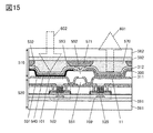
- FIG. 15 is a diagram illustrating an example of a cross section of the pixel illustrated in FIG. 14A.
- the layer 510 has, as the light emitting device 11, the EL element shown in FIG. 14B.
- the photoelectric conversion device 101 has the organic photoconductive film shown in FIG. 14C.
- the layer 520 includes an OS transistor, and in FIG. 15, the transistor 102 connected to the photoelectric conversion device 101 and the transistor 109 connected to the light-emitting device 11 are illustrated with the structure illustrated in FIG. 9C as an example.
- the electrode 312 corresponds to the reference potential line (GND) shown in FIG. 9C.
- the layer 532 corresponds to a power supply line (wiring 121).
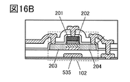
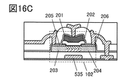
- FIG. 16A shows details of the OS transistor.
- the OS transistor illustrated in FIG. 16A has a self-aligned structure in which an insulating layer is provided over a stack of an oxide semiconductor layer and a conductive layer and a groove reaching the semiconductor layer is provided to form a source electrode 205 and a drain electrode 206. is there.
- the OS transistor can include a channel formation region formed in the oxide semiconductor layer 207, a source region 203, and a drain region 204, as well as a gate electrode 201 and a gate insulating film 202. At least the gate insulating film 202 and the gate electrode 201 are provided in the groove. An oxide semiconductor layer 208 may be further provided in the groove.
- the OS transistor may have a self-aligned structure in which the source region 203 and the drain region 204 are formed in the semiconductor layer using the gate electrode 201 as a mask.
- a non-self-aligned top-gate transistor having a region where the source electrode 205 or the drain electrode 206 and the gate electrode 201 overlap with each other may be used.
- the transistors 102 and 109 each have a structure including a back gate 535
- the transistors 102 and 109 may have a structure without a back gate.
- the back gate 535 may be electrically connected to the front gates of the transistors provided to face each other as in the cross-sectional view in the channel width direction of the transistor illustrated in FIG. 16D. Note that FIG. 16D shows the transistor of FIG. 16A as an example, but transistors of other structures are similar. Further, the back gate 535 may be configured to be able to supply a fixed potential different from that of the front gate.
- Planarization films 551 and 552 are provided over the transistors 102 and 109.
- the light emitting device 11 (the electrode 311, the EL layer 300, the electrode 312) and the photoelectric conversion device 101 (the layer 531, the layer 540, and the layer 532) are provided on the surface where the uneven portions generated in the transistor and the contact portion are flattened by the planarizing films 551 and 552. Is provided.
- a low-resistance conductive film such as a metal can be used for the electrode 311 and the layer 531.
- a light-transmitting conductive film which transmits near-infrared light can be used for the electrode 312 and the layer 532.
- the electrode 312 and the layer 532 include indium oxide containing tungsten oxide, indium zinc oxide containing tungsten oxide, indium oxide containing titanium oxide, indium tin oxide, indium tin oxide containing titanium oxide, and indium.
- a light-transmitting conductive material such as zinc oxide or indium tin oxide to which silicon oxide is added can be used.
- light 601 is emitted from the light emitting device 11 included in the layer 510 to the outside, and reflected light 602 is received by the photoelectric conversion device 101 included in the layer 510.
- a protective layer 553 may be provided over the light emitting device 11 and the photoelectric conversion device 101 so that oxygen, hydrogen, moisture, carbon dioxide, and the like do not enter the light emitting device 11 and the photoelectric conversion device 101.
- an inorganic insulating film such as silicon nitride, silicon nitride oxide, aluminum oxide, aluminum nitride, aluminum oxynitride, aluminum nitride oxide, or DLC (Diamond Like Carbon).
- a sealing layer 570 between the protective layer 553 and the substrate 582 for sealing.
- an ultraviolet curable resin or a thermosetting resin can be used in addition to an inert gas such as nitrogen or argon.
- PVC polyvinyl chloride
- acrylic resin polyimide
- epoxy resin silicone resin
- silicone resin can be used.
- Resin, PVB polyvinyl butyral
- EVA ethylene vinyl acetate
- the sealing layer 570 may include a desiccant.
- a light-blocking layer 571 between the protective layer 553 and the substrate 582 at and near the boundary between the light-emitting device 11 and the photoelectric conversion device 101.
- Part of the light emitted from the light emitting device 11 may be scattered or reflected by the sealing layer 570, the protective layer 553, the substrate 582, and the like, and may be received by the photoelectric conversion device 101.
- the light-blocking layer 571 is preferably formed using a metal having a high reflectance of light having a wavelength to be used, a resin having a high absorptance, or the like.
- the substrates 581 and 582 are support substrates.
- the layer 591 is preferably provided between the substrate 581 and a region where a transistor or the like is provided.
- a layer 592 is preferably provided between the substrate 582 and a region where the sealing layer 570 is provided.
- the layers 591 and 592 are buffer layers for peeling the structure from the hard substrate, and for example, a resin such as polyimide having heat resistance and a small linear expansion coefficient can be used. Note that the layer 591 may function as a supporting substrate without providing the substrate 581. Alternatively, the substrate 582 may not be provided and the layer 592 may function as a supporting substrate.
- FIG. 17A1 is an infrared spectroscope for analyzing brain function. As shown in FIG. 17A2, the human body is worn so as to cover the head.
- the imaging device 912 of one embodiment of the present invention has flexibility and can be attached to the inner curved surface of the helmet-type housing 911. It should be noted that the image pickup device 912 may be attached only to a necessary portion instead of the entire inner surface of the housing 911. Further, the infrared spectroscopic device can have a data recording memory, a control LSI, a battery, and the like. Data extraction and power supply can be performed via the external interface 913.
- the infrared spectroscopic device detects nerve activity in the cerebral cortex by comparing the absorbance of infrared light having an absorption peak of oxyhemoglobin and the absorbance of infrared light having a reduction peak of reduced hemoglobin (taking a difference). can do. It can be used for grasping and researching injuries and diseases because it can know the active part of the brain and the intensity of the activity. Since the imaging device 912 of one embodiment of the present invention has a light source and is thin, a thin and lightweight infrared spectroscopic device can be formed.
- FIG. 17B1 is an infrared spectroscopic device that has the same basic function as that of FIG. 17A1 but analyzes brain functions of different shapes and uses.
- the infrared spectroscopic device includes two image pickup devices 922, a battery 923, and a wireless communication unit 924, which are built in the band 921.
- the human body is attached to a part of the head by utilizing the elasticity of the band 921.
- the band 921 is made of an elastic material such as resin or metal. Power can be supplied from the battery 923, and data can be transmitted and received through the wireless communication unit 924.
- the infrared spectroscopic device is small and lightweight, and can be used to detect activity in a specific part of the brain.
- FIG. 18A is a blood oxygen concentration meter.
- a finger is placed on the detection unit 932 provided in the housing 931 and an image is taken by the image pickup device 934 arranged immediately below the detection unit 932.
- the imaging result is displayed on the display unit 933 provided on the top of the housing 931.
- the blood oxygen concentration meter can calculate the oxygen concentration in blood from the difference in the absorbance of oxyhemoglobin and reduced hemoglobin with respect to light of two different wavelengths. Since the imaging device 912 of one embodiment of the present invention has a light source and is thin, a thin and lightweight blood oxygen analyzer can be formed.
- FIG. 18B shows a food sorting device, which has a housing 941, operation buttons 942, a display portion 943, a light-shielding hood 944, and the like.
- a light-shielding hood 944 provided around the light receiving unit to the food material to be inspected such as fruit and capturing the image, foreign matter mixed in the food material, insects, cavities inside the food material, decay and the like can be detected.
- an infrared spectrum can be obtained from the difference between a plurality of detected infrared lights, and the sugar content of the food material can also be detected.
- the food sorting machine can sort defective products and grades and judge the harvest time.
- the imaging device 945 of one embodiment of the present invention which is provided in the light-receiving portion does not require a light source; thus, a thin, lightweight, and portable food selection device can be formed at low cost.
Landscapes
- Engineering & Computer Science (AREA)
- Multimedia (AREA)
- Signal Processing (AREA)
- Health & Medical Sciences (AREA)
- Life Sciences & Earth Sciences (AREA)
- Physics & Mathematics (AREA)
- General Health & Medical Sciences (AREA)
- Surgery (AREA)
- Medical Informatics (AREA)
- Veterinary Medicine (AREA)
- Public Health (AREA)
- Animal Behavior & Ethology (AREA)
- Biophysics (AREA)
- Pathology (AREA)
- Biomedical Technology (AREA)
- Heart & Thoracic Surgery (AREA)
- Molecular Biology (AREA)
- Toxicology (AREA)
- Spectroscopy & Molecular Physics (AREA)
- Human Computer Interaction (AREA)
- Vascular Medicine (AREA)
- Theoretical Computer Science (AREA)
- General Physics & Mathematics (AREA)
- Transforming Light Signals Into Electric Signals (AREA)
- Solid State Image Pick-Up Elements (AREA)
- Thin Film Transistor (AREA)
Priority Applications (5)
| Application Number | Priority Date | Filing Date | Title |
|---|---|---|---|
| CN201980066901.1A CN112840639B (zh) | 2018-10-11 | 2019-10-07 | 摄像装置及电子设备 |
| US17/282,129 US11595594B2 (en) | 2018-10-11 | 2019-10-07 | Imaging apparatus and electronic device |
| KR1020217014032A KR102823435B1 (ko) | 2018-10-11 | 2019-10-07 | 촬상 장치 및 전자 기기 |
| JP2020550958A JP7396995B2 (ja) | 2018-10-11 | 2019-10-07 | 撮像装置および電子機器 |
| JP2023203094A JP7633363B2 (ja) | 2018-10-11 | 2023-11-30 | 半導体装置 |
Applications Claiming Priority (2)
| Application Number | Priority Date | Filing Date | Title |
|---|---|---|---|
| JP2018192666 | 2018-10-11 | ||
| JP2018-192666 | 2018-10-11 |
Publications (1)
| Publication Number | Publication Date |
|---|---|
| WO2020075031A1 true WO2020075031A1 (ja) | 2020-04-16 |
Family
ID=70164547
Family Applications (1)
| Application Number | Title | Priority Date | Filing Date |
|---|---|---|---|
| PCT/IB2019/058506 Ceased WO2020075031A1 (ja) | 2018-10-11 | 2019-10-07 | 撮像装置および電子機器 |
Country Status (5)
| Country | Link |
|---|---|
| US (1) | US11595594B2 (enExample) |
| JP (2) | JP7396995B2 (enExample) |
| KR (1) | KR102823435B1 (enExample) |
| CN (1) | CN112840639B (enExample) |
| WO (1) | WO2020075031A1 (enExample) |
Cited By (1)
| Publication number | Priority date | Publication date | Assignee | Title |
|---|---|---|---|---|
| JP2025031750A (ja) * | 2020-04-17 | 2025-03-07 | 株式会社半導体エネルギー研究所 | 撮像装置 |
Families Citing this family (3)
| Publication number | Priority date | Publication date | Assignee | Title |
|---|---|---|---|---|
| JP7530898B2 (ja) | 2019-07-17 | 2024-08-08 | 株式会社半導体エネルギー研究所 | 表示装置 |
| KR20230047392A (ko) * | 2020-08-03 | 2023-04-07 | 가부시키가이샤 한도오따이 에네루기 켄큐쇼 | 반도체 장치 및 전자 기기 |
| US20240248217A1 (en) * | 2022-01-25 | 2024-07-25 | Beijing Boe Sensor Technology Co., Ltd. | Detection substrate and ray detector |
Citations (3)
| Publication number | Priority date | Publication date | Assignee | Title |
|---|---|---|---|---|
| JP2011119711A (ja) * | 2009-11-06 | 2011-06-16 | Semiconductor Energy Lab Co Ltd | 半導体装置 |
| JP2011118887A (ja) * | 2009-11-06 | 2011-06-16 | Semiconductor Energy Lab Co Ltd | タッチパネル及びタッチパネルの駆動方法 |
| JP2018136491A (ja) * | 2017-02-23 | 2018-08-30 | 株式会社半導体エネルギー研究所 | 画像表示システムおよび電子機器 |
Family Cites Families (16)
| Publication number | Priority date | Publication date | Assignee | Title |
|---|---|---|---|---|
| DE60030959T2 (de) * | 1999-01-29 | 2007-06-14 | Hamamatsu Photonics K.K., Hamamatsu | Photodetektorvorrichtung |
| JP2006025451A (ja) * | 1999-03-30 | 2006-01-26 | Sharp Corp | 相関2重サンプリング回路およびそれを用いた増幅型固体撮像装置 |
| JP4119052B2 (ja) * | 1999-07-16 | 2008-07-16 | 浜松ホトニクス株式会社 | 光検出装置 |
| JP2004014673A (ja) * | 2002-06-05 | 2004-01-15 | Nippon Hoso Kyokai <Nhk> | 固体撮像装置及びそれを用いたカメラ装置 |
| JP5810575B2 (ja) * | 2011-03-25 | 2015-11-11 | ソニー株式会社 | 固体撮像装置、および、その製造方法、電子機器 |
| KR101976228B1 (ko) | 2011-09-22 | 2019-05-07 | 가부시키가이샤 한도오따이 에네루기 켄큐쇼 | 광 검출 장치 및 광 검출 장치의 구동 방법 |
| KR101871235B1 (ko) * | 2012-06-05 | 2018-06-27 | 삼성전자주식회사 | 깊이 영상 생성 방법 및 장치, 깊이 영상 처리 방법 및 장치 |
| DE102013217278B4 (de) * | 2012-09-12 | 2017-03-30 | Semiconductor Energy Laboratory Co., Ltd. | Photodetektorschaltung, Bildgebungsvorrichtung und Verfahren zum Ansteuern einer Photodetektorschaltung |
| JP2016029795A (ja) | 2014-07-18 | 2016-03-03 | 株式会社半導体エネルギー研究所 | 半導体装置、撮像装置及び電子機器 |
| WO2016046685A1 (en) | 2014-09-26 | 2016-03-31 | Semiconductor Energy Laboratory Co., Ltd. | Imaging device |
| TWI677973B (zh) * | 2014-11-17 | 2019-11-21 | 國立大學法人東北大學 | 光感測器之訊號讀出方法以及攝像裝置之訊號讀出方法 |
| US9773832B2 (en) | 2014-12-10 | 2017-09-26 | Semiconductor Energy Laboratory Co., Ltd. | Semiconductor device and electronic device |
| US9876946B2 (en) | 2015-08-03 | 2018-01-23 | Semiconductor Energy Laboratory Co., Ltd. | Imaging device and electronic device |
| JP6956784B2 (ja) | 2017-06-08 | 2021-11-02 | 株式会社半導体エネルギー研究所 | 撮像装置 |
| JP7003126B2 (ja) | 2017-06-14 | 2022-01-20 | 株式会社半導体エネルギー研究所 | 撮像装置、及び電子機器 |
| CN108391071B (zh) * | 2017-11-23 | 2020-04-14 | 南京邮电大学 | 一种采用二次相关双采样技术的spad阵列级读出电路 |
-
2019
- 2019-10-07 KR KR1020217014032A patent/KR102823435B1/ko active Active
- 2019-10-07 WO PCT/IB2019/058506 patent/WO2020075031A1/ja not_active Ceased
- 2019-10-07 US US17/282,129 patent/US11595594B2/en active Active
- 2019-10-07 JP JP2020550958A patent/JP7396995B2/ja active Active
- 2019-10-07 CN CN201980066901.1A patent/CN112840639B/zh active Active
-
2023
- 2023-11-30 JP JP2023203094A patent/JP7633363B2/ja active Active
Patent Citations (3)
| Publication number | Priority date | Publication date | Assignee | Title |
|---|---|---|---|---|
| JP2011119711A (ja) * | 2009-11-06 | 2011-06-16 | Semiconductor Energy Lab Co Ltd | 半導体装置 |
| JP2011118887A (ja) * | 2009-11-06 | 2011-06-16 | Semiconductor Energy Lab Co Ltd | タッチパネル及びタッチパネルの駆動方法 |
| JP2018136491A (ja) * | 2017-02-23 | 2018-08-30 | 株式会社半導体エネルギー研究所 | 画像表示システムおよび電子機器 |
Cited By (2)
| Publication number | Priority date | Publication date | Assignee | Title |
|---|---|---|---|---|
| JP2025031750A (ja) * | 2020-04-17 | 2025-03-07 | 株式会社半導体エネルギー研究所 | 撮像装置 |
| JP7770524B2 (ja) | 2020-04-17 | 2025-11-14 | 株式会社半導体エネルギー研究所 | 撮像装置 |
Also Published As
| Publication number | Publication date |
|---|---|
| CN112840639A (zh) | 2021-05-25 |
| US11595594B2 (en) | 2023-02-28 |
| JPWO2020075031A1 (ja) | 2021-10-14 |
| KR20210069714A (ko) | 2021-06-11 |
| JP2024015126A (ja) | 2024-02-01 |
| JP7396995B2 (ja) | 2023-12-12 |
| KR102823435B1 (ko) | 2025-06-19 |
| JP7633363B2 (ja) | 2025-02-19 |
| US20210377463A1 (en) | 2021-12-02 |
| CN112840639B (zh) | 2024-10-15 |
Similar Documents
| Publication | Publication Date | Title |
|---|---|---|
| US11997910B2 (en) | Sensor device and semiconductor device | |
| US12165049B2 (en) | Imaging device, imaging module, electronic device, and imaging system | |
| JP7633363B2 (ja) | 半導体装置 | |
| JP7121840B2 (ja) | 画像検出モジュール | |
| JP7350753B2 (ja) | 撮像装置および電子機器 | |
| JP2025031750A (ja) | 撮像装置 | |
| US20250168527A1 (en) | Imaging device and electronic device | |
| JP7132076B2 (ja) | Ct装置 | |
| US12074179B2 (en) | Imaging device and electronic device | |
| US12132060B2 (en) | Imaging device and electronic device | |
| KR102879659B1 (ko) | 촬상 장치 또는 촬상 시스템 | |
| US12495629B2 (en) | Imaging device, electronic device, and moving object |
Legal Events
| Date | Code | Title | Description |
|---|---|---|---|
| 121 | Ep: the epo has been informed by wipo that ep was designated in this application |
Ref document number: 19871397 Country of ref document: EP Kind code of ref document: A1 |
|
| ENP | Entry into the national phase |
Ref document number: 2020550958 Country of ref document: JP Kind code of ref document: A |
|
| NENP | Non-entry into the national phase |
Ref country code: DE |
|
| ENP | Entry into the national phase |
Ref document number: 20217014032 Country of ref document: KR Kind code of ref document: A |
|
| 122 | Ep: pct application non-entry in european phase |
Ref document number: 19871397 Country of ref document: EP Kind code of ref document: A1 |