WO2020071046A1 - 再生装置及び再生方法 - Google Patents
再生装置及び再生方法Info
- Publication number
- WO2020071046A1 WO2020071046A1 PCT/JP2019/034806 JP2019034806W WO2020071046A1 WO 2020071046 A1 WO2020071046 A1 WO 2020071046A1 JP 2019034806 W JP2019034806 W JP 2019034806W WO 2020071046 A1 WO2020071046 A1 WO 2020071046A1
- Authority
- WO
- WIPO (PCT)
- Prior art keywords
- light
- signal
- phase
- difference
- phase correction
- Prior art date
- Legal status (The legal status is an assumption and is not a legal conclusion. Google has not performed a legal analysis and makes no representation as to the accuracy of the status listed.)
- Ceased
Links
Images




Classifications
-
- G—PHYSICS
- G11—INFORMATION STORAGE
- G11B—INFORMATION STORAGE BASED ON RELATIVE MOVEMENT BETWEEN RECORD CARRIER AND TRANSDUCER
- G11B7/00—Recording or reproducing by optical means, e.g. recording using a thermal beam of optical radiation by modifying optical properties or the physical structure, reproducing using an optical beam at lower power by sensing optical properties; Record carriers therefor
- G11B7/004—Recording, reproducing or erasing methods; Read, write or erase circuits therefor
- G11B7/005—Reproducing
-
- G—PHYSICS
- G11—INFORMATION STORAGE
- G11B—INFORMATION STORAGE BASED ON RELATIVE MOVEMENT BETWEEN RECORD CARRIER AND TRANSDUCER
- G11B7/00—Recording or reproducing by optical means, e.g. recording using a thermal beam of optical radiation by modifying optical properties or the physical structure, reproducing using an optical beam at lower power by sensing optical properties; Record carriers therefor
- G11B7/12—Heads, e.g. forming of the optical beam spot or modulation of the optical beam
- G11B7/13—Optical detectors therefor
-
- G—PHYSICS
- G11—INFORMATION STORAGE
- G11B—INFORMATION STORAGE BASED ON RELATIVE MOVEMENT BETWEEN RECORD CARRIER AND TRANSDUCER
- G11B7/00—Recording or reproducing by optical means, e.g. recording using a thermal beam of optical radiation by modifying optical properties or the physical structure, reproducing using an optical beam at lower power by sensing optical properties; Record carriers therefor
- G11B7/12—Heads, e.g. forming of the optical beam spot or modulation of the optical beam
- G11B7/135—Means for guiding the beam from the source to the record carrier or from the record carrier to the detector
Definitions
- the present technology relates to a reproducing apparatus and a reproducing method applied to reproducing an optical medium such as an optical disk.
- Patent Literature 1 as a homodyne method for detecting light in which signal light and reference light interfere with each other, detection is performed for four sets of signal light and reference light whose phase differences are different by 90 degrees. Has been. More specifically, detection is performed for each of a pair of signal light and reference light having a phase difference of 0 degree, 90 degrees, 180 degrees, and 270 degrees. Each of these detections is performed by detecting the light intensity of the light that caused the signal light and the reference light to interfere with each other. Further, a servo for correcting a change in the optical path length due to surface shake of the optical disk is applied.
- Patent Literature 2 describes that an optical path length difference between a signal light and a reference light is obtained by calculation.
- a component of the signal light amplified according to the light intensity of the reference light can be obtained as a reproduction signal.
- the SNR of the reproduced signal can be improved.
- phase offset optical path length difference
- ⁇ has phase fluctuations at relatively low frequencies and phase fluctuations at higher frequencies due to surface deflection of the optical disk.
- the phase fluctuation in the high band occurs due to, for example, minute irregularities (surface roughness) on the disk surface.
- the phase fluctuation is higher than the servo band, and the phase fluctuation in a high frequency band cannot be completely removed.
- phase unwrapping process and a filter process are applied to remove noise of the detected phase difference signal.
- phase unwrapping may not be performed correctly due to the influence of noise, and a large error may be added to the filter processing result.
- an object of the present technology is to provide a reproducing apparatus and a reproducing method that employ a homodyne detection method and that can prevent the phase unwrapping from being performed incorrectly due to the influence of noise.
- the present technology obtains signal light by irradiating light emitted from a light source to a recording medium, generates reference light from light emitted from the light source, and superimposes the signal light and the reference light.
- the phase correction unit is A phase correction circuit, a phase detection circuit that detects a phase correction residual from an output signal of the phase correction circuit, and a filter processing circuit that filters the phase correction residual, and feeds back an output of the filter processing circuit to the phase correction circuit.
- a playback device comprising: a path;
- the present technology obtains signal light by irradiating light emitted from a light source to a recording medium, generates reference light from light emitted from the light source, and superimposes the signal light and the reference light.
- An optical system that respectively generates a pair of a third signal light and a reference light having a phase difference of about 270 ° and a fourth signal light and a reference light having a phase difference of about 270 °;
- a pair of the first signal light and the reference light is a first light receiving element, a pair of the second signal light and the reference light is a second light receiving element, a pair of the third signal light and the reference light is a third light receiving element,
- a light receiving unit that receives a set of the signal light and the reference light by a fourth light receiving element,
- a first difference signal a which is a difference between a first light receiving signal obtained by the first light receiving element and a second light receiving signal obtained by the second light receiving element; a third light receiving signal obtained by the third
- a phase correction unit that is supplied with the first difference signal a and the second difference signal b and corrects an optical path length difference ⁇ between the signal light and the reference light;
- the phase correction unit is A phase correction circuit, a phase detection circuit that detects a phase correction residual from an output signal of the phase correction circuit, and a filter processing circuit that filters the phase correction residual, and feeds back an output of the filter processing circuit to the phase correction circuit.
- a playback device comprising: a path;
- the phase difference between the signal light and the reference light is sequentially updated, and the phase correction residual is substantially at the center of zero degree, so that the correction phase can be calculated correctly without the need for phase unwrapping and land / groove recording.
- the optical recording medium of the system can be reproduced favorably by using the homodyne detection method.
- FIG. 1 is a diagram showing a configuration of an example of a conventional reproducing apparatus.
- FIG. 2 is a diagram showing a configuration of another example of the conventional reproducing apparatus.
- FIG. 3 is a block diagram showing a configuration of a phase detection unit of another example of the conventional reproducing apparatus.
- 4A and 4B are schematic diagrams used to describe the phase unwrapping process.
- 5A, 5B, and 5C are schematic diagrams used to explain the problem of the phase unwrapping process.
- FIG. 6 is a diagram illustrating a configuration of the first embodiment of the present technology.
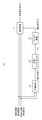
- FIG. 7 is a block diagram illustrating a configuration of the phase correction unit according to the first embodiment of the present technology.
- FIG. 8 is a block diagram illustrating a configuration of a phase correction unit according to the second embodiment of the present technology.
- FIG. 9 is a diagram showing a configuration of still another example of the conventional reproducing apparatus.
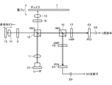
- FIG. 1 shows an example of the configuration of a conventional reproducing apparatus using homodyne detection.
- An optical recording medium hereinafter, referred to as an optical disk
- Laser light irradiation is performed on the optical disk 1 that is rotationally driven, and a recorded signal is reproduced.
- the optical disc 1 is a so-called write-once optical disc on which information is recorded by forming recording marks, for example.
- the “upper layer side” refers to the upper layer side when the surface on which the laser beam from the reproducing apparatus enters is the upper surface. That is, in this case, the laser light is incident on the optical disc 1 from the cover layer side.
- the substrate is made of, for example, a resin such as polycarbonate, and has an uneven cross-sectional shape on the upper surface side.
- the cover layer is provided for protecting the recording layer. A mark array is formed on the optical disc 1 to be reproduced.
- the laser (semiconductor laser) 10 serving as a laser light source for reproduction is provided in the optical system of the reproduction apparatus.
- the laser light emitted from the laser 10 is converted into parallel light via a collimation lens 11 and then enters a polarization beam splitter 12.
- the polarization beam splitter 12 is configured to transmit, for example, P-polarized light and reflect S-polarized light.
- the laser beam transmitted through the polarizing beam splitter 12 is irradiated to the recording layer of the optical disc 1 through the quarter-wave plate 8 and the objective lens 13 held by the biaxial actuator so as to be focused.
- the laser light reflected by the recording layer of the optical disc 1 is incident on the polarization beam splitter 12 via the objective lens 13 and the quarter-wave plate 8.
- the quarter-wave plate 8 twice the polarization plane is rotated by 90 degrees. Therefore, the return light from the disk 1 is reflected by the polarization beam splitter 12 without being transmitted, and travels toward the half beam splitter 16.
- the optical path of the signal light is shown by a broken line.
- the laser light emitted from the laser 10 and reflected by the polarization beam splitter 12 functions as reference light in the homodyne detection method.
- the reference light reflected by the polarization beam splitter 12 passes through the quarter-wave plate 9 and the lens 14 and is reflected by the mirror 15, passes again through the lens 14 and the quarter-wave plate 9, and is transmitted to the polarization beam splitter 12.
- the light reflected by the polarization beam splitter 12 from the laser 10 and traveling toward the mirror 15 passes through the quarter-wave plate 9 twice in a round trip between the polarization beam splitter 12 and the mirror 15 so that the polarization plane is rotated by 90 degrees. I do.
- the reflected light from the mirror 15 is transmitted without being reflected by the polarization beam splitter 12 and travels to the half beam splitter 16.
- the optical path of the reference light is shown by a solid line.
- the mirror 15 is displaced by a reference light servo as shown by an arrow, thereby making it possible to expand and contract the optical path length of the reference light.
- the signal light and the reference light are incident on the polarization beam splitter 12, the signal light is reflected by the polarization beam splitter 12, and the reference light passes through the polarization beam splitter 12.
- the polarization beam splitter 12 emits the signal light and the reference light in the same direction in a superimposed state. Specifically, in this case, the signal light and the reference light are emitted in the same direction while being superimposed so that their optical axes coincide.
- the reference light is so-called coherent light.
- the superimposed light of the signal light and the reference light output from the polarization beam splitter 12 enters the half beam splitter 16.
- the half beam splitter 16 splits incident light into reflected light and transmitted light at a ratio of approximately 1: 1.
- the superimposed light of the signal light and the reference light transmitted through the half beam splitter 16 is incident on the polarization beam splitter 18 via the half-wave plate 17.
- the superimposed light of the signal light and the reference light reflected by the half beam splitter 16 is incident on the polarization beam splitter 20 via the quarter-wave plate 19.
- the wavelength plate 17 and 1 / wavelength plate 19 can rotate the plane of polarization. Therefore, by combining the half-wave plate 17 and the polarization beam splitter 18, the ratio of the amount of light split by the polarization beam splitter 18 can be adjusted. Similarly, the ⁇ ⁇ wavelength plate 19 can adjust the ratio of the amount of light split by the polarization beam splitter 20.
- the amount of light split by each of the polarizing beam splitters 18 and 20 is set to be approximately 1: 1.
- the light reflected by the polarization beam splitter 18 is incident on a light detection unit 21 (PD1) as a first light receiving element, and the light transmitted through the polarization beam splitter 18 is detected by a light detection unit 22 (PD2) as a second light reception element. ).
- the light reflected by the polarization beam splitter 20 is incident on the light detection unit 23 (PD3) as a third light receiving element, and the light transmitted through the polarization beam splitter 20 is detected by the light detection unit 24 (PD4) as a fourth light reception element. ).
- the first light reception signal I output from the light detection unit 21 and passed through the capacitor 25 and the second light reception signal J output from the light detection unit 22 and passed through the capacitor 26 are supplied to the subtracter 27a.
- the third light reception signal K output from the light detection unit 23 and passed through the capacitor 28 and the fourth light reception signal L output from the light detection unit 24 and passed through the capacitor 29 are supplied to the subtracter 27b.
- the capacitors 25 to 29 are provided to supply each light receiving signal to the subtractor 27a or 27b by AC coupling.
- the first difference signal a and the second difference signal b are in an orthogonal relationship, and the first difference signal a is referred to as a 0 ° phase side signal, and the second difference signal b is referred to as a 90 ° phase side signal.
- the output signal (0 ° phase side) of the subtracter 27a is supplied to the decoding processing unit 30, and the decoding signal is output from the decoding processing unit 30.
- the output signal of the subtractor 27a (0 ° phase side) and the output signal of the subtracter 27b (90 ° phase side) are supplied to the phase detection circuit 31.
- a servo error signal is output from the phase detection circuit 31.
- the servo error signal is supplied to a servo mechanism (not shown) of the mirror 15 via the servo filter 32. The mirror 15 is displaced according to the servo error signal to control the optical path length of the reference light.
- the reference light servo mechanism as described above can correct a phase fluctuation at a relatively low frequency such as a surface shake of the optical disk 1, but cannot remove a phase fluctuation at a high frequency.
- the phase fluctuation in the high band occurs due to, for example, minute irregularities (surface roughness) on the disk surface.
- FIG. 2 shows the configuration of another example of a reproducing apparatus using the conventional homodyne detection.
- the 0 ° phase side signal a and the 90 ° phase side signal b are supplied to the phase correction unit 33, and the phase corrected signal is supplied to the decoding processing unit 30. Note that the above-described reference light servo may be used together.
- FIG. 3 shows the configuration of the phase correction unit 33.
- the 0 ° phase side signal a and the 90 ° phase side signal b are supplied to the rotation processing circuit 41 and the phase detection circuit 42.
- a phase correction output A is obtained from the rotation processing circuit 41.
- the phase detection circuit 42 performs the following arithmetic processing.
- the obtained detected phase ⁇ is supplied to the phase unwrapping circuit 43.
- the phase unwrapping circuit 43 is a circuit that reproduces the original signal from the signal whose phase has been turned back.
- An unwrapped phase ⁇ u is obtained from the output of the phase unwrapping circuit 43.
- Phase ⁇ u is supplied to the filter processing circuit 44.
- the filter processing circuit 44 is provided for noise reduction, and is, for example, a low-pass filter.
- the correction phase ⁇ a extracted from the filter processing circuit 44 is supplied to the rotation processing circuit 41.
- the following processing is performed in the rotation processing circuit 41 to obtain the phase correction output A in which the phase fluctuation is corrected.
- A a ⁇ cos ( ⁇ a) + b ⁇ sin ( ⁇ a)
- the processing of the phase unwrapping circuit 43 will be described with reference to FIG.
- the phase unwrapping process is a process in which a level difference between two consecutive samples is obtained, and when the obtained level difference is larger than a predetermined value, it is determined that the phase has been folded, and the folding is corrected.
- the detection phase ⁇ obtained by the phase detection circuit 42 can only take a value in the range of (+ 180 ° to ⁇ 180 °). Is folded back.
- the phase unwrapping circuit 43 determines that a phase aliasing has occurred since the difference between the sample near + 180 ° and the sample near ⁇ 180 ° exceeds a predetermined value, and as shown in FIG. 4B , A phase unwrapping process for correcting aliasing is performed.
- the dotted line indicates the average value of the detected phases.
- phase unwrapping process is based on the premise that the detected phase ⁇ changes continuously, there is a problem that the phase unwrapping process is not performed correctly when noise is present.
- two samples (Pi-1 and Pi) which are continuous in time and have a value close to + 180 ° may have a value lower than + 180 ° and a value higher than + 180 ° due to the influence of noise. It is possible.
- the data wrapped at + 180 ° has the original value of the sample Pi ⁇ 1 and the sample Pi wrapped at ⁇ 180 °.
- the difference between two consecutive samplings Pi-1 and Pi is calculated, but since the difference does not become large, it is not possible to detect the folding, and data after the phase unwrapping process as shown in FIG. 5C is generated. . 5C is different from the correct value of the detected phase ⁇ .
- the present technology performs phase correction by arithmetic processing, and has a system configuration as shown in FIG. It has a configuration for homodyne detection as in the conventional reproducing apparatus shown in FIG. In order to avoid redundant description, corresponding components have the same reference characters allotted, and description thereof will not be repeated.
- the phase correction unit 50 will be described with reference to FIG.
- the 0 ° phase side signal a (n) and the 90 ° phase side signal b (n) are supplied to the rotation processing circuit 51.
- n represents a discrete time.
- the rotation processing circuit 51 performs a rotation operation on the two input signals.
- the following phase-corrected outputs are extracted from the rotation processing circuit 51.
- ⁇ a (n) is the correction phase fed back from the filter processing circuit 53.
- a (n) a (n) cos ( ⁇ a (n)) ⁇ b (n) sin ( ⁇ a (n))
- B (n) a (n) sin ( ⁇ a (n)) + b (n) cos ( ⁇ a (n))
- phase correction output A (n) is taken out as an output and supplied to the phase detection circuit 52.
- phase correction output B (n) is also supplied to the phase detection circuit 52, and the detection phase ⁇ (n) is obtained by the following calculation.
- ⁇ (n) 0.5 atan ⁇ (A (n) 2 ⁇ B (n) 2 ), A (n) B (n) ⁇
- the obtained detection phase ⁇ (n) is for detecting a phase after the phase correction by the rotation processing circuit 51, and the obtained detection phase ⁇ (n) is a phase correction residual.
- the detected phase ⁇ (n) is supplied to the filter processing circuit 53.
- the filter processing circuit 53 is a low-pass filter that forms a correction phase ⁇ a by performing, for example, a double integration operation as shown in the following equation.
- the correction phase ⁇ a formed by the filter processing circuit 53 is fed back to the rotation processing circuit 51.
- ⁇ t is the output of the first integration
- ⁇ a is the output of the second integration.
- k1 to k4 are constants.
- the phase correction residual becomes substantially 0 ° center by repeating the feedback processing, so that the phase unwrapping processing becomes unnecessary.
- the phase correction unit 50 does not perform the phase unwrapping process, it is possible to prevent the phase unwrapping process from being erroneous due to the above-described noise. Further, by repeating the feedback loop of the phase correction, the correction phase ⁇ a converges to a correct value.
- Second Embodiment> A second embodiment of the present technology will be described. It has a system configuration similar to that of the first embodiment (see FIG. 6). Further, the phase correction unit 60 according to the second embodiment has a configuration shown in FIG. Like the phase correction unit 50 of the first embodiment, a feedback path from the filter processing circuit 63 to the rotation processing circuit 61 is provided.
- the phase correction unit 60 will be described with reference to FIG.
- the 0 ° phase side signal a (n) and the 90 ° phase side signal b (n) are supplied to the rotation processing circuit 61.
- n represents a discrete time.
- the rotation processing circuit 61 performs a rotation operation on the two input signals. From the rotation processing circuit 61, the following phase correction outputs A (n) and B (n) are taken out.
- ⁇ a (n) is the correction phase fed back from the filter processing circuit 63.
- a (n) a (n) cos ( ⁇ a (n)) ⁇ b (n) sin ( ⁇ a (n))
- B (n) a (n) sin ( ⁇ a (n)) + b (n) cos ( ⁇ a (n))
- phase correction outputs A (n) and B (n) are supplied to the phase detection circuit 62.
- the correlation between the two is obtained by using a value obtained by multiplying two signals after phase correction whose phase relations are orthogonal to each other, and this is detected as the detected phase ⁇ (n) (phase (Correction residual).
- the detected phase ⁇ (n) obtained by the phase detection circuit 62 is supplied to the filter processing circuit 63.
- the filter processing circuit 63 is configured to perform integration twice as in the first embodiment.
- the correction phase ⁇ a formed by the filter processing circuit 63 is fed back to the rotation processing circuit 61.
- the phase unwrapping process since the phase unwrapping process is not performed, it is possible to prevent the phase unwrapping process from being erroneous due to the above-described noise. Further, by repeating the feedback loop of the phase correction, the correction phase ⁇ a converges to a correct value. Further, since there is no need to perform the operation of the trigonometric function as in the first embodiment, the configuration of the phase detection circuit 62 can be simplified.
- the present invention can be applied to a configuration in which no differential operation is performed.
- 9 corresponding to FIG. 2 are denoted by the same reference numerals.
- a signal light is obtained by irradiating a light emitted from a light source to a recording medium, and a reference light is generated from the light emitted from the light source, and the signal light and the reference light are superimposed.
- An optical system that generates a set of a first signal light and a reference light having a phase difference of about 0 ° with respect to the light and a set of a third signal light and a reference light having a phase difference of about 90 ° with the light
- a light receiving unit that receives a set of the first signal light and the reference light with a first light receiving element and a set of the third signal light and the reference light with a third light receiving element
- a phase correction unit for supplying a first light receiving signal obtained by the first light receiving element and a third light receiving signal obtained by the third light receiving element, and correcting an optical path length difference ⁇ between the signal light and the reference light;
- the phase correction unit A phase correction circuit, a phase detection circuit for detecting a phase correction residual from an output signal of the phase correction circuit, and a filter processing circuit for filtering the phase correction residual, wherein an output of the filter processing circuit is subjected to the phase correction.
- a signal light is obtained by irradiating a light emitted from a light source to a recording medium, and a reference light is generated from the light emitted from the light source, and the signal light and the reference light are superimposed.
- a set of the first signal light and the reference light is a first light receiving element, a set of the second signal light and the reference light is a second light receiving element, and a set of the third signal light and the reference light is a third light receiving element.
- a light receiving unit that receives a set of the fourth signal light and the reference light by a fourth light receiving element, A first difference signal a which is a difference between a first light receiving signal obtained by the first light receiving element and a second light receiving signal obtained by the second light receiving element; a third light receiving signal obtained by the third light receiving element; An arithmetic unit for calculating a difference between the fourth light receiving signals obtained by the fourth light receiving element and obtaining a second difference signal b having a phase relationship orthogonal to the first difference signal a; A phase correction unit that is supplied with the first difference signal a and the second difference signal b and that corrects an optical path length difference ⁇ between the signal light and the reference light; The phase correction unit, A phase correction circuit, a phase detection circuit for detecting a phase correction residual from an output signal of the phase correction circuit, and a filter processing circuit for filtering the phase correction residual, wherein an output of the filter processing circuit is subjected to the phase correction.
- the phase correction circuit forms the outputs A (n) and B (n) after the phase correction by the following calculation when the feedback correction phase is ⁇ a and the discrete time is n (1) or (2).
- a playback device according to claim 1.
- a (n) a (n) cos ( ⁇ a (n)) ⁇ b (n) sin ( ⁇ a (n))
- B (n) a (n) sin ( ⁇ a (n)) + b (n) cos ( ⁇ a (n))
- ⁇ (n) 0.5 atan ⁇ (A (n) 2 ⁇ B (n) 2 ), A (n) B (n) ⁇ (5)
- ⁇ (n) A (n) B (n) (6)
- the reproducing device according to any one of (1) to (5), wherein the reference light is generated by reflecting light emitted from the light source with a mirror.
- a signal light is obtained by irradiating a light emitted from a light source to a recording medium, and a reference light is generated from the light emitted from the light source, and the signal light and the reference light are superimposed.
- a pair of a first signal light and a reference light having a phase difference of approximately 0 ° with respect to the light, and a pair of a third signal light and a reference light having a phase difference of approximately 90 ° are generated.
- a set of the first signal light and the reference light is received by a first light receiving element, and a set of the third signal light and the reference light is received by a third light receiving element;
- a first light receiving signal obtained by the first light receiving element and a third light receiving signal obtained by the third light receiving element are supplied, and an optical path length difference ⁇ between the signal light and the reference light is corrected by a phase correcting unit;
- the phase correction unit A reproducing method for detecting a phase correction residual from an output signal of the phase correction, filtering the phase correction residual, and feeding back the filtered output to a phase correction circuit.
- a signal light is obtained by irradiating a light emitted from a light source to a recording medium, and a reference light is generated from the light emitted from the light source, and the signal light and the reference light are superimposed.
- a pair of the first signal light and the reference light having a phase difference of about 0 ° with respect to the light, a pair of the second signal light and the reference light having a phase difference of about 180 °, and Generating a set of a third signal light and a reference light having a phase difference and a set of a fourth signal light and a reference light having a phase difference of approximately 270 °;
- a pair of the first signal light and the reference light is a first light receiving element, a pair of the second signal light and the reference light is a second light receiving element, and a pair of the third signal light and the reference light is a third light receiving element.
- a first difference signal a which is a difference between a first light receiving signal obtained by the first light receiving element and a second light receiving signal obtained by the second light receiving element; a third light receiving signal obtained by the third light receiving element; Calculating a second difference signal b, which is a difference between the fourth light receiving signals obtained by the fourth light receiving element and whose phase relationship is orthogonal to the first difference signal a;
- the first difference signal a and the second difference signal b are supplied, and the optical path length difference ⁇ between the signal light and the reference light is corrected by a phase correction unit,
- the phase correction unit A reproduction method comprising: detecting a phase correction residual from an output signal of a phase correction, filtering the phase correction residual, and feeding back the filtered output to the phase correction circuit.
Landscapes
- Physics & Mathematics (AREA)
- Optics & Photonics (AREA)
- Optical Recording Or Reproduction (AREA)
- Optical Head (AREA)
Abstract
第1差分信号aと、第1差分信号aと位相関係が直交する第2差分信号bを求める演算部と、第1差分信号a及び第2差分信号bが供給され、信号光と参照光の光路長差θを補正する位相補正部とを有し、位相補正部は、位相補正回路と、位相補正回路の出力信号から位相補正残差を検出する位相検出回路と、位相補正残差をフィルタ処理するフィルタ処理回路からなり、フィルタ処理回路の出力を位相補正回路にフィードバックする経路とを備える再生装置である。 図7
Description
本技術は、光ディスク等の光媒体を再生するのに適用される再生装置及び再生方法に関する。
例えば多層光ディスクを再生する場合、信号光量の低下が生じ、信号の読み取りにエラーが発生する可能性が高くなる。この問題を解決するため、光の干渉を利用して検出信号を増幅するホモダイン検出法が知られている(特許文献1及び特許文献2参照)。
特許文献1では、信号光と参照光とを干渉させた光を検波するホモダイン方式として、それぞれその位相差が90度ずつ異なるようにされた4つの信号光・参照光の組について検波を行うようにされている。具体的には、位相差がそれぞれ0度、90度、180度、270度とされた信号光・参照光の組について、それぞれ検波を行うものである。これらの各検波は、信号光と参照光とを干渉させた光についての光強度をそれぞれ検出することで行われる。さらに、光ディスクの面ブレによる光路長の変化を補正するサーボをかけるようになされている。特許文献2には、演算によって信号光と参照光の光路長差を求めることが記載されている。
ホモダイン方式では、参照光の光強度に応じて増幅された信号光の成分を、再生信号として得ることができる。このように信号光が増幅されることで、再生信号のSNRを改善することができる。
ホモダイン方式では信号光と参照光の光路長差(位相オフセット)θが存在すると、所期の効果が得られなくなる。θには、光ディスクの面振れによる比較的低域周波数の位相変動と、より高い周波数の位相変動とがある。高域の位相変動は例えばディスク表面の微小な凹凸(表面の粗さ)に起因して発生する。特許文献1に記載のサーボ制御の場合、位相変動がサーボ帯域より高く、高域の位相変動を除去しきれない。
高域の位相変動は、光路長の長さをミラーの変位によって変化させる方式では除去できないので、信号処理によって位相変動を除去するようになされる。このために位相を補正する場合には、検出された位相差信号のノイズを除去するために、位相アンラッピング処理及びフィルタ処理が適用される。しかしながら、ノイズの影響により位相のアンラッピングが正しく行われず、フィルタ処理結果に大きな誤差を付加してしまう場合があった。
したがって、本技術の目的は、ホモダイン検出方式を採用すると共に、位相のアンラッピングがノイズの影響を受けて正しく行われないことを防止できる再生装置及び再生方法を提供することにある。
本技術は、光源より発せられた光を記録媒体に対して照射することによって信号光を得、且つ光源より発せられた光から参照光を生成し、信号光と参照光とを重ね合わせた重ね合わせ光に対し、ほぼ0°の位相差を与えた第1の信号光と参照光の組と、ほぼ90°の位相差を与えた第3の信号光と参照光の組をそれぞれ生成する光学系と、
第1の信号光と参照光の組を第1受光素子、第3の信号光と参照光の組を第3受光素子によってそれぞれ受光する受光部と、
第1受光素子で得られる第1受光信号及び第3受光素子で得られる第3受光信号が供給され、信号光と参照光の光路長差θを補正する位相補正部とを有し、
位相補正部は、
位相補正回路と、位相補正回路の出力信号から位相補正残差を検出する位相検出回路と、位相補正残差をフィルタ処理するフィルタ処理回路からなり、フィルタ処理回路の出力を位相補正回路にフィードバックする経路と
を備える再生装置である。
本技術は、光源より発せられた光を記録媒体に対して照射することによって信号光を得、且つ光源より発せられた光から参照光を生成し、信号光と参照光とを重ね合わせた重ね合わせ光に対し、ほぼ0°の位相差を与えた第1の信号光と参照光の組と、ほぼ180°の位相差を与えた第2の信号光と参照光の組と、ほぼ90°の位相差を与えた第3の信号光と参照光の組と、ほぼ270°の位相差を与えた第4の信号光と参照光の組をそれぞれ生成する光学系と、
第1の信号光と参照光の組を第1受光素子、第2の信号光と参照光の組を第2受光素子、第3の信号光と参照光の組を第3受光素子、第4の信号光と参照光の組を第4受光素子によってそれぞれ受光する受光部と、
第1受光素子で得られる第1受光信号と第2受光素子で得られる第2受光信号の差分である第1差分信号aと、第3受光素子で得られる第3受光信号と第4受光素子で得られる第4受光信号の差分であり、第1差分信号aと位相関係が直交する第2差分信号bを求める演算部と、
第1差分信号a及び第2差分信号bが供給され、信号光と参照光の光路長差θを補正する位相補正部とを有し、
位相補正部は、
位相補正回路と、位相補正回路の出力信号から位相補正残差を検出する位相検出回路と、位相補正残差をフィルタ処理するフィルタ処理回路からなり、フィルタ処理回路の出力を位相補正回路にフィードバックする経路と
を備える再生装置である。
第1の信号光と参照光の組を第1受光素子、第3の信号光と参照光の組を第3受光素子によってそれぞれ受光する受光部と、
第1受光素子で得られる第1受光信号及び第3受光素子で得られる第3受光信号が供給され、信号光と参照光の光路長差θを補正する位相補正部とを有し、
位相補正部は、
位相補正回路と、位相補正回路の出力信号から位相補正残差を検出する位相検出回路と、位相補正残差をフィルタ処理するフィルタ処理回路からなり、フィルタ処理回路の出力を位相補正回路にフィードバックする経路と
を備える再生装置である。
本技術は、光源より発せられた光を記録媒体に対して照射することによって信号光を得、且つ光源より発せられた光から参照光を生成し、信号光と参照光とを重ね合わせた重ね合わせ光に対し、ほぼ0°の位相差を与えた第1の信号光と参照光の組と、ほぼ180°の位相差を与えた第2の信号光と参照光の組と、ほぼ90°の位相差を与えた第3の信号光と参照光の組と、ほぼ270°の位相差を与えた第4の信号光と参照光の組をそれぞれ生成する光学系と、
第1の信号光と参照光の組を第1受光素子、第2の信号光と参照光の組を第2受光素子、第3の信号光と参照光の組を第3受光素子、第4の信号光と参照光の組を第4受光素子によってそれぞれ受光する受光部と、
第1受光素子で得られる第1受光信号と第2受光素子で得られる第2受光信号の差分である第1差分信号aと、第3受光素子で得られる第3受光信号と第4受光素子で得られる第4受光信号の差分であり、第1差分信号aと位相関係が直交する第2差分信号bを求める演算部と、
第1差分信号a及び第2差分信号bが供給され、信号光と参照光の光路長差θを補正する位相補正部とを有し、
位相補正部は、
位相補正回路と、位相補正回路の出力信号から位相補正残差を検出する位相検出回路と、位相補正残差をフィルタ処理するフィルタ処理回路からなり、フィルタ処理回路の出力を位相補正回路にフィードバックする経路と
を備える再生装置である。
少なくとも一つの実施形態によれば、信号光及び参照光の位相差は逐次的に更新され、位相補正残差は概ね零度中心となるため位相アンラッピング不要で正しく補正位相を算出できランド/グルーブ記録方式の光記録媒体をホモダイン検出方法を使用して良好に再生することができる。なお、ここに記載された効果は必ずしも限定されるものではなく、本技術中に記載されたいずれかの効果又はそれらと異質な効果であっても良い。また、以下の説明における例示された効果により本技術の内容が限定して解釈されるものではない。
以下に説明する実施の形態は、本技術の好適な具体例であり、技術的に好ましい種々の限定が付されている。しかしながら、本技術の範囲は、以下の説明において、特に本技術を限定する旨の記載がない限り、これらの実施の形態に限定されないものとする。
なお、本技術の説明は、下記の順序にしたがってなされる。
<1.従来のホモダイン検出を使用した再生装置>
<2.第1の実施の形態>
<3.第2の実施の形態>
<4.変形例>
なお、本技術の説明は、下記の順序にしたがってなされる。
<1.従来のホモダイン検出を使用した再生装置>
<2.第1の実施の形態>
<3.第2の実施の形態>
<4.変形例>
<1.従来のホモダイン検出を使用した再生装置>
図1は、従来のホモダイン検出を使用した再生装置の一例の構成を示す。光記録媒体(以下、光ディスクと称する)1は、再生装置に装填されると、スピンドルモータによって回転駆動される。回転駆動される光ディスク1に対するレーザ光照射が行われて記録信号の再生が行われる。光ディスク1は、例えば記録マークの形成により情報が記録されたいわゆる追記型の光ディスクとされる。
図1は、従来のホモダイン検出を使用した再生装置の一例の構成を示す。光記録媒体(以下、光ディスクと称する)1は、再生装置に装填されると、スピンドルモータによって回転駆動される。回転駆動される光ディスク1に対するレーザ光照射が行われて記録信号の再生が行われる。光ディスク1は、例えば記録マークの形成により情報が記録されたいわゆる追記型の光ディスクとされる。
光ディスク1には、上層側から順にカバー層、記録層(反射膜)、基板が形成されている。ここで、「上層側」とは、再生装置側からのレーザ光が入射する面を上面としたときの上層側を指す。つまりこの場合、光ディスク1に対しては、カバー層側からレーザ光が入射することになる。基板は、例えばポリカーボネートなどの樹脂で構成され、その上面側には凹凸の断面形状が与えられている。カバー層は、記録層の保護のために設けられている。再生対象とする光ディスク1には、マーク列が形成されている。
再生装置の光学系には、再生のためのレーザ光源となるレーザ(半導体レーザ)10が設けられている。レーザ10より出射されたレーザ光は、コリメーションレンズ11を介して平行光となるようにされた後、偏光ビームスプリッタ12に入射される。
偏光ビームスプリッタ12は、例えばP偏光を透過しS偏光を反射するように構成されている。偏光ビームスプリッタ12を透過したレーザ光は、1/4波長板8及び2軸アクチュエータにより保持された対物レンズ13を介して光ディスク1の記録層に集光するようにして照射される。光ディスク1の記録層で反射されたレーザ光が対物レンズ13及び1/4波長板8を介して偏光ビームスプリッタ12に入射される。1/4波長板8を2回通過することによって偏光面が90度回転する。このため、ディスク1からの戻り光は偏光ビームスプリッタ12で透過されずに反射されハーフビームスプリッタ16へ向かう。図では、信号光の光路を破線で示している。
レーザ10より出射され、偏光ビームスプリッタ12で反射したレーザ光は、ホモダイン検出方式における参照光として機能する。偏光ビームスプリッタ12で反射した参照光は、1/4波長板9及びレンズ14を通ってミラー15にて反射されて、再びレンズ14及び1/4波長板9を通過して偏光ビームスプリッタ12に入射される。レーザ10から偏光ビームスプリッタ12で反射されてミラー15に向かう光は、偏光ビームスプリッタ12とミラー15との間の往復で1/4波長板9を2回通過することにより偏光面が90度回転する。このため、ミラー15からの反射光は偏光ビームスプリッタ12で反射されずに透過されハーフビームスプリッタ16へ向かう。図では、参照光の光路を実線で示している。ミラー15は、矢印で示すように、参照光サーボによって変位され、これによって参照光の光路長を伸縮可能とされている。
偏光ビームスプリッタ12に対して信号光及び参照光が入射され、信号光が偏光ビームスプリッタ12によって反射され、参照光が偏光ビームスプリッタ12を通過する。偏光ビームスプリッタ12によって、これら信号光と参照光とが重ね合わされた状態で同方向に出射される。具体的にこの場合、信号光と参照光とはそれらの光軸が一致するように重ね合わされた状態で同方向に出射される。ここで、参照光は、いわゆるコヒーレント光である。
偏光ビームスプリッタ12から出力された信号光と参照光の重ね合わせ光は、ハーフビームスプリッタ16に入射される。ハーフビームスプリッタ16は、入射光をほぼ1:1の割合で反射光と透過光とに分割する。
ハーフビームスプリッタ16を透過した信号光と参照光の重ね合わせ光は、1/2波長板17を介して偏光ビームスプリッタ18に入射される。一方、ハーフビームスプリッタ16で反射した信号光と参照光の重ね合わせ光は、1/4波長板19を介して偏光ビームスプリッタ20に入射される。
1/2波長板17及び1/4波長板19は、偏光面を回転させることが可能とされている。したがって、1/2波長板17と偏光ビームスプリッタ18とを組み合わせることによって、偏光ビームスプリッタ18によって分岐される光量の比を調整することができる。同様に、1/4波長板19によって、偏光ビームスプリッタ20によって分岐される光量の比を調整することができる。
偏光ビームスプリッタ18及び20のそれぞれによって分岐される光の光量がほぼ1:1となるようにされる。偏光ビームスプリッタ18によって反射された光が第1の受光素子としての光検出部21(PD1)に入射され、偏光ビームスプリッタ18を透過した光が第2の受光素子としての光検出部22(PD2)に入射される。偏光ビームスプリッタ20によって反射された光が第3の受光素子としての光検出部23(PD3)に入射され、偏光ビームスプリッタ20を透過した光が第4の受光素子としての光検出部24(PD4)に入射される。
光検出部21から出力され、コンデンサ25を介された第1受光信号Iと、光検出部22から出力され、コンデンサ26を介された第2受光信号Jが減算器27aに供給される。また、光検出部23から出力され、コンデンサ28を介された第3受光信号Kと、光検出部24から出力され、コンデンサ29を介された第4受光信号Lが減算器27bに供給される。コンデンサ25~29は、交流結合でもって各受光信号を減算器27a又は27bに供給するために設けられている。減算器27aが(a=I-J)の第1差分信号aを発生し、減算器27bが(b=K-L)の第2差分信号bを発生する。第1差分信号a及び第2差分信号bは、直交関係にあり、第1差分信号aを0°位相側信号と称し、第2差分信号bを90°位相側信号と称する。
減算器27aの出力信号(0°位相側)が復号処理部30に供給され、復号処理部30から再生信号が出力される。また、減算器27aの出力信号(0°位相側)と減算器27bの出力信号(90°位相側)が位相検出回路31に供給される。位相検出回路31からサーボエラー信号が出力される。サーボエラー信号がサーボフィルタ32を介してミラー15のサーボ機構(不図示)に供給される。ミラー15がサーボエラー信号に応じて変位し、参照光の光路長を制御するようになされる。
上述したような参照光サーボ機構は、光ディスク1の面ブレのような比較的低い周波数の位相変動を補正することができるが、高い周波数の位相変動を除去できない問題がある。高域の位相変動は例えばディスク表面の微小な凹凸(表面の粗さ)に起因して発生する。
図2は、従来のホモダイン検出を使用した再生装置の他の例の構成を示す。減算器27aの出力に0°位相側信号a(=I-J)を取り出し、減算器27bの出力に90°位相側信号b(=K-L)を取り出す構成は、図1と同様であるので、対応する構成要素に対して同一の参照符号を付してその説明を省略する。
0°位相側信号a及び90°位相側信号bが位相補正部33に供給され、位相補正された信号が復号処理部30に供給される。なお、上述した参照光サーボを併用するようにしてもよい。
図3に位相補正部33の構成を示す。0°位相側信号a及び90°位相側信号bが回転処理回路41及び位相検出回路42に供給される。回転処理回路41から位相補正出力Aが得られる。位相検出回路42は、検出位相をθで表すと、下記の演算処理を行う。
sin(2θ)=2ab
cos(2θ)=a2 -b2
cos(2θ)=a2 -b2
これらの式を使用して検出位相θを求める。
θ=0.5atan{(a2 -b2 ),ab}
θ=0.5atan{(a2 -b2 ),ab}
求められた検出位相θが位相アンラッピング回路43に供給される。位相アンラッピング回路43は、位相が折り返された信号から元の信号を再現する回路である。位相アンラッピング回路43の出力にアンラッピングされた位相θuが得られる。
位相θuがフィルタ処理回路44に供給される。フィルタ処理回路44は、ノイズ低減のために設けられており、例えばローパスフィルタである。フィルタ処理回路44から取り出された補正位相θaが回転処理回路41に供給される。回転処理回路41において、下記の演算処理がなされ、位相変動が補正された位相補正出力Aが得られる。
A=a・cos(θa)+b・sin(θa)
図4を参照して位相アンラッピング回路43の処理について説明する。位相アンラッピング処理は、連続する2サンプルの間のレベル差を求め、求められたレベル差が所定の値より大きい場合には、位相が折り返されたと判定し、この折り返しを補正する処理である。例えば図4Aに示すように、位相検出回路42によって求められる検出位相θは、(+180°~-180°)の範囲の値しかとることができないので、例えば+180°を超える値が-180°側に折り返されている。
位相アンラッピング回路43では、一例として、+180°付近のサンプルと-180°付近のサンプルの差が所定の値を超えるので、位相の折り返しが発生していると判定し、図4Bに示すように、折り返しを補正する位相アンラッピング処理を行う。なお、図4において、点線は、検出位相の平均値を表している。
上述した位相アンラッピング処理は、検出位相θが連続的に変化することを前提としているために、ノイズが存在すると位相アンラッピング処理が正しく行われない問題がある。例えば図5Aに示すように、時間的に連続し、+180°に近い値の2サンプル(Pi-1 及びPi)がノイズの影響によって、+180°より低い値と+180°より高い値を持つ場合がありうる。
このようなデータの場合、+180°でラッピングされたデータは、図5Bに示すように、サンプルPi-1が元の値で、サンプルPiが-180°で折り返されたものとなる。連続する2つのサンプリングPi-1及びPiの差が計算されるが、差が大きくならないために、折り返されたことが検出できず、図5Cに示すような位相アンラッピング処理後のデータが発生する。この図5Cのデータは、検出位相θの正しい値と異なったものである。
<2.第1の実施の形態>
本技術の第1の実施形態について説明する。本技術は、演算処理によって位相補正を行うもので、図6に示すようなシステムの構成を有する。図2に示す従来の再生装置と同様にホモダイン検出の構成を有する。重複した説明を避けるために、対応する構成要素に同一の参照符号を付してその説明を省略する。0°位相側信号a(=I-J)及び90°位相側信号b(=K-L)が本技術による位相補正部50に供給され、位相補正出力が形成される。
本技術の第1の実施形態について説明する。本技術は、演算処理によって位相補正を行うもので、図6に示すようなシステムの構成を有する。図2に示す従来の再生装置と同様にホモダイン検出の構成を有する。重複した説明を避けるために、対応する構成要素に同一の参照符号を付してその説明を省略する。0°位相側信号a(=I-J)及び90°位相側信号b(=K-L)が本技術による位相補正部50に供給され、位相補正出力が形成される。
図7を参照して位相補正部50について説明する。0°位相側信号a(n)及び90°位相側信号b(n)が回転処理回路51に供給される。なお、nは、離散時刻を表す。回転処理回路51は、二つの入力信号の回転演算を行う。回転処理回路51からは、次に示す位相補正後の出力(位相補正出力A(n)及びB(n))が取り出される。ここで、θa(n)は、フィルタ処理回路53からフィードバックされた補正位相である。
A(n)=a(n)cos(θa(n))-b(n)sin(θa(n))
B(n)=a(n)sin(θa(n))+b(n)cos(θa(n))
B(n)=a(n)sin(θa(n))+b(n)cos(θa(n))
位相補正出力A(n)が出力として取り出されると共に、位相検出回路52に供給される。位相検出回路52に対して位相補正出力B(n)も供給され、下記の演算によって検出位相θ(n)が求められる。
sin(2θ(n))=2A(n)B(n)
cos(2θ(n))=A(n)2 -B(n)2
これらの式から次のように検出位相θ(n)が求まる。
cos(2θ(n))=A(n)2 -B(n)2
これらの式から次のように検出位相θ(n)が求まる。
θ(n)=0.5atan{(A(n)2 -B(n)2),A(n)B(n)}
求められた検出位相θ(n)は、回転処理回路51による位相補正後に、位相を検出するものであり、求められた検出位相θ(n)は、位相補正残差である。検出位相θ(n)がフィルタ処理回路53に供給される。フィルタ処理回路53は、例えば次の式に示すような2回積分の演算を行って補正位相θaを形成するローパスフィルタである。フィルタ処理回路53によって形成された補正位相θaが回転処理回路51にフィードバックされる。θtが1回目の積分の出力であり、θaが2回目の積分の出力である。式において、k1 ~k4 は、定数である。
θt(n+1)=k1θt(n)+k2θ(n)
θa(n+1)=k3θa(n)+k4θt(n+1)
θa(n+1)=k3θa(n)+k4θt(n+1)
第1の実施形態では、フィードバック処理を繰り返すことによって、位相補正残差が概ね0°中心となるため、位相アンラッピング処理が不要となる。このように、位相補正部50が位相アンラッピング処理を行わないので、上述したようなノイズによって位相アンラッピング処理が誤ることを防止することができる。また、位相補正のフィードバックループを繰り返すことによって、補正位相θaが正しい値に収束することになる。
<3.第2の実施の形態>
本技術の第2の実施形態について説明する。第1の実施形態と同様のシステムの構成(図6参照)を有する。また、第2の実施形態の位相補正部60は、図8に示す構成を有する。第1の実施形態の位相補正部50と同様に、フィルタ処理回路63から回転処理回路61に対するフィードバック経路が設けられている。
本技術の第2の実施形態について説明する。第1の実施形態と同様のシステムの構成(図6参照)を有する。また、第2の実施形態の位相補正部60は、図8に示す構成を有する。第1の実施形態の位相補正部50と同様に、フィルタ処理回路63から回転処理回路61に対するフィードバック経路が設けられている。
図8を参照して位相補正部60について説明する。0°位相側信号a(n)及び90°位相側信号b(n)が回転処理回路61に供給される。なお、nは、離散時刻を表す。回転処理回路61は、二つの入力信号の回転演算を行う。回転処理回路61からは、次に示す位相補正出力A(n)及びB(n)が取り出される。ここで、θa(n)は、フィルタ処理回路63からフィードバックされた補正位相である。
A(n)=a(n)cos(θa(n))-b(n)sin(θa(n))
B(n)=a(n)sin(θa(n))+b(n)cos(θa(n))
B(n)=a(n)sin(θa(n))+b(n)cos(θa(n))
これらの位相補正出力A(n)及びB(n)が位相検出回路62に供給される。位相検出回路62においては、次に示すように、位相関係が直交する二つの位相補正後の信号を乗算した値を用いて両者間の相関性を求め、これを検出位相θ(n)(位相補正残差)として用いる。
θ(n)=A(n)B(n)
位相検出回路62によって求められた検出位相θ(n)がフィルタ処理回路63に供給される。フィルタ処理回路63は、第1の実施形態と同様に2回積分を行う構成とされている。フィルタ処理回路63によって形成された補正位相θaが回転処理回路61にフィードバックされる。
かかる第2の実施形態では、位相アンラッピング処理を行わないので、上述したようなノイズによって位相アンラッピング処理が誤ることを防止することができる。また、位相補正のフィードバックループを繰り返すことによって、補正位相θaが正しい値に収束することになる。さらに、第1の実施形態のような三角関数の演算を行う必要がないので、位相検出回路62の構成を簡略化することが可能となる。
<5.変形例>
以上、本技術の実施の形態について具体的に説明したが、上述の各実施の形態に限定されるものではなく、本技術の技術的思想に基づく各種の変形が可能である。
以上、本技術の実施の形態について具体的に説明したが、上述の各実施の形態に限定されるものではなく、本技術の技術的思想に基づく各種の変形が可能である。
また、上述の実施の形態の構成、方法、工程、形状、材料及び数値などは、本技術の主旨を逸脱しない限り、互いに組み合わせることが可能である。
例えば本発明は、図9に示すように、差動演算を行わない構成に対しても適用することができる。図2と対応する図9における構成要素には、同一の参照符号を付して示す。
なお、本技術は、以下のような構成も取ることができる。
(1)
光源より発せられた光を記録媒体に対して照射することによって信号光を得、且つ前記光源より発せられた光から参照光を生成し、前記信号光と前記参照光とを重ね合わせた重ね合わせ光に対し、ほぼ0°の位相差を与えた第1の信号光と参照光の組と、ほぼ90°の位相差を与えた第3の信号光と参照光の組をそれぞれ生成する光学系と、
前記第1の信号光と参照光の組を第1受光素子、前記第3の信号光と参照光の組を第3受光素子によってそれぞれ受光する受光部と、
前記第1受光素子で得られる第1受光信号及び前記第3受光素子で得られる第3受光信号が供給され、前記信号光と参照光の光路長差θを補正する位相補正部とを有し、
前記位相補正部は、
位相補正回路と、前記位相補正回路の出力信号から位相補正残差を検出する位相検出回路と、前記位相補正残差をフィルタ処理するフィルタ処理回路からなり、前記フィルタ処理回路の出力を前記位相補正回路にフィードバックする経路と
を備える再生装置。
(2)
光源より発せられた光を記録媒体に対して照射することによって信号光を得、且つ前記光源より発せられた光から参照光を生成し、前記信号光と前記参照光とを重ね合わせた重ね合わせ光に対し、ほぼ0°の位相差を与えた第1の信号光と参照光の組と、ほぼ180°の位相差を与えた第2の信号光と参照光の組と、ほぼ90°の位相差を与えた第3の信号光と参照光の組と、ほぼ270°の位相差を与えた第4の信号光と参照光の組をそれぞれ生成する光学系と、
前記第1の信号光と参照光の組を第1受光素子、前記第2の信号光と参照光の組を第2受光素子、前記第3の信号光と参照光の組を第3受光素子、前記第4の信号光と参照光の組を第4受光素子によってそれぞれ受光する受光部と、
前記第1受光素子で得られる第1受光信号と前記第2受光素子で得られる第2受光信号の差分である第1差分信号aと、前記第3受光素子で得られる第3受光信号と前記第4受光素子で得られる第4受光信号の差分であり、前記第1差分信号aと位相関係が直交する第2差分信号bを求める演算部と、
前記第1差分信号a及び前記第2差分信号bが供給され、前記信号光と参照光の光路長差θを補正する位相補正部とを有し、
前記位相補正部は、
位相補正回路と、前記位相補正回路の出力信号から位相補正残差を検出する位相検出回路と、前記位相補正残差をフィルタ処理するフィルタ処理回路からなり、前記フィルタ処理回路の出力を前記位相補正回路にフィードバックする経路と
を備える再生装置。
(3)
前記位相補正回路は、フィードバックされた補正位相をθa、離散時刻をnとする場合に次の演算によって位相補正後の出力A(n)及びB(n)を形成する(1)又は(2)に記載の再生装置。
A(n)=a(n)cos(θa(n))-b(n)sin(θa(n))
B(n)=a(n)sin(θa(n))+b(n)cos(θa(n))
(4)
前記位相検出回路は、フィードバックされた補正位相をθa、離散時刻をnとする場合に次の演算によって位相補正残差θ(n)を形成する(3)に記載の再生装置。
θ(n)=0.5atan{(A(n)2 -B(n)2),A(n)B(n)}
(5)
前記位相検出回路は、フィードバックされた補正位相をθa、離散時刻をnとする場合に次の演算によって位相補正残差θ(n)を形成する(3)に記載の再生装置。
θ(n)=A(n)B(n)
(6)
前記参照光は、前記光源より発せられた光をミラーにて反射させることによって生成される(1)から(5)のいずれかに記載の再生装置。
(7)
光源より発せられた光を記録媒体に対して照射することによって信号光を得、且つ前記光源より発せられた光から参照光を生成し、前記信号光と前記参照光とを重ね合わせた重ね合わせ光に対し、ほぼ0°の位相差を与えた第1の信号光と参照光の組と、ほぼ90°の位相差を与えた第3の信号光と参照光の組をそれぞれ生成し、
前記第1の信号光と参照光の組を第1受光素子、前記第3の信号光と参照光の組を第3受光素子によってそれぞれ受光し、
前記第1受光素子で得られる第1受光信号及び前記第3受光素子で得られる第3受光信号が供給され、前記信号光と参照光の光路長差θを位相補正部によって補正し、
前記位相補正部は、
位相補正の出力信号から位相補正残差を検出し、前記位相補正残差をフィルタ処理し、前記フィルタ処理出力を位相補正回路にフィードバックする処理を行う
再生方法。
(8)
光源より発せられた光を記録媒体に対して照射することによって信号光を得、且つ前記光源より発せられた光から参照光を生成し、前記信号光と前記参照光とを重ね合わせた重ね合わせ光に対し、ほぼ0°の位相差を与えた第1の信号光と参照光の組と、ほぼ180°の位相差を与えた第2の信号光と参照光の組と、ほぼ90°の位相差を与えた第3の信号光と参照光の組と、ほぼ270°の位相差を与えた第4の信号光と参照光の組をそれぞれ生成し、
前記第1の信号光と参照光の組を第1受光素子、前記第2の信号光と参照光の組を第2受光素子、前記第3の信号光と参照光の組を第3受光素子、前記第4の信号光と参照光の組を第4受光素子によってそれぞれ受光し、
前記第1受光素子で得られる第1受光信号と前記第2受光素子で得られる第2受光信号の差分である第1差分信号aと、前記第3受光素子で得られる第3受光信号と前記第4受光素子で得られる第4受光信号の差分であり、前記第1差分信号aと位相関係が直交する第2差分信号bを求め、
前記第1差分信号a及び前記第2差分信号bが供給され、前記信号光と参照光の光路長差θを位相補正部によって補正し、
前記位相補正部は、
位相補正の出力信号から位相補正残差を検出し、前記位相補正残差をフィルタ処理し、前記フィルタ処理出力を前記位相補正回路にフィードバックする処理を行う
再生方法。
(1)
光源より発せられた光を記録媒体に対して照射することによって信号光を得、且つ前記光源より発せられた光から参照光を生成し、前記信号光と前記参照光とを重ね合わせた重ね合わせ光に対し、ほぼ0°の位相差を与えた第1の信号光と参照光の組と、ほぼ90°の位相差を与えた第3の信号光と参照光の組をそれぞれ生成する光学系と、
前記第1の信号光と参照光の組を第1受光素子、前記第3の信号光と参照光の組を第3受光素子によってそれぞれ受光する受光部と、
前記第1受光素子で得られる第1受光信号及び前記第3受光素子で得られる第3受光信号が供給され、前記信号光と参照光の光路長差θを補正する位相補正部とを有し、
前記位相補正部は、
位相補正回路と、前記位相補正回路の出力信号から位相補正残差を検出する位相検出回路と、前記位相補正残差をフィルタ処理するフィルタ処理回路からなり、前記フィルタ処理回路の出力を前記位相補正回路にフィードバックする経路と
を備える再生装置。
(2)
光源より発せられた光を記録媒体に対して照射することによって信号光を得、且つ前記光源より発せられた光から参照光を生成し、前記信号光と前記参照光とを重ね合わせた重ね合わせ光に対し、ほぼ0°の位相差を与えた第1の信号光と参照光の組と、ほぼ180°の位相差を与えた第2の信号光と参照光の組と、ほぼ90°の位相差を与えた第3の信号光と参照光の組と、ほぼ270°の位相差を与えた第4の信号光と参照光の組をそれぞれ生成する光学系と、
前記第1の信号光と参照光の組を第1受光素子、前記第2の信号光と参照光の組を第2受光素子、前記第3の信号光と参照光の組を第3受光素子、前記第4の信号光と参照光の組を第4受光素子によってそれぞれ受光する受光部と、
前記第1受光素子で得られる第1受光信号と前記第2受光素子で得られる第2受光信号の差分である第1差分信号aと、前記第3受光素子で得られる第3受光信号と前記第4受光素子で得られる第4受光信号の差分であり、前記第1差分信号aと位相関係が直交する第2差分信号bを求める演算部と、
前記第1差分信号a及び前記第2差分信号bが供給され、前記信号光と参照光の光路長差θを補正する位相補正部とを有し、
前記位相補正部は、
位相補正回路と、前記位相補正回路の出力信号から位相補正残差を検出する位相検出回路と、前記位相補正残差をフィルタ処理するフィルタ処理回路からなり、前記フィルタ処理回路の出力を前記位相補正回路にフィードバックする経路と
を備える再生装置。
(3)
前記位相補正回路は、フィードバックされた補正位相をθa、離散時刻をnとする場合に次の演算によって位相補正後の出力A(n)及びB(n)を形成する(1)又は(2)に記載の再生装置。
A(n)=a(n)cos(θa(n))-b(n)sin(θa(n))
B(n)=a(n)sin(θa(n))+b(n)cos(θa(n))
(4)
前記位相検出回路は、フィードバックされた補正位相をθa、離散時刻をnとする場合に次の演算によって位相補正残差θ(n)を形成する(3)に記載の再生装置。
θ(n)=0.5atan{(A(n)2 -B(n)2),A(n)B(n)}
(5)
前記位相検出回路は、フィードバックされた補正位相をθa、離散時刻をnとする場合に次の演算によって位相補正残差θ(n)を形成する(3)に記載の再生装置。
θ(n)=A(n)B(n)
(6)
前記参照光は、前記光源より発せられた光をミラーにて反射させることによって生成される(1)から(5)のいずれかに記載の再生装置。
(7)
光源より発せられた光を記録媒体に対して照射することによって信号光を得、且つ前記光源より発せられた光から参照光を生成し、前記信号光と前記参照光とを重ね合わせた重ね合わせ光に対し、ほぼ0°の位相差を与えた第1の信号光と参照光の組と、ほぼ90°の位相差を与えた第3の信号光と参照光の組をそれぞれ生成し、
前記第1の信号光と参照光の組を第1受光素子、前記第3の信号光と参照光の組を第3受光素子によってそれぞれ受光し、
前記第1受光素子で得られる第1受光信号及び前記第3受光素子で得られる第3受光信号が供給され、前記信号光と参照光の光路長差θを位相補正部によって補正し、
前記位相補正部は、
位相補正の出力信号から位相補正残差を検出し、前記位相補正残差をフィルタ処理し、前記フィルタ処理出力を位相補正回路にフィードバックする処理を行う
再生方法。
(8)
光源より発せられた光を記録媒体に対して照射することによって信号光を得、且つ前記光源より発せられた光から参照光を生成し、前記信号光と前記参照光とを重ね合わせた重ね合わせ光に対し、ほぼ0°の位相差を与えた第1の信号光と参照光の組と、ほぼ180°の位相差を与えた第2の信号光と参照光の組と、ほぼ90°の位相差を与えた第3の信号光と参照光の組と、ほぼ270°の位相差を与えた第4の信号光と参照光の組をそれぞれ生成し、
前記第1の信号光と参照光の組を第1受光素子、前記第2の信号光と参照光の組を第2受光素子、前記第3の信号光と参照光の組を第3受光素子、前記第4の信号光と参照光の組を第4受光素子によってそれぞれ受光し、
前記第1受光素子で得られる第1受光信号と前記第2受光素子で得られる第2受光信号の差分である第1差分信号aと、前記第3受光素子で得られる第3受光信号と前記第4受光素子で得られる第4受光信号の差分であり、前記第1差分信号aと位相関係が直交する第2差分信号bを求め、
前記第1差分信号a及び前記第2差分信号bが供給され、前記信号光と参照光の光路長差θを位相補正部によって補正し、
前記位相補正部は、
位相補正の出力信号から位相補正残差を検出し、前記位相補正残差をフィルタ処理し、前記フィルタ処理出力を前記位相補正回路にフィードバックする処理を行う
再生方法。
1・・・光ディスク、12,20・・・偏光ビームスプリッタ、15・・・ミラー、
21,22,23,24・・・光検出部、27a,27b・・・減算器、
30・・・信号処理部、33,50,60・・・位相検出部、
41,51,61・・・回転処理回路、43・・・位相アンラッピング回路、
44,53,63・・・フィルタ処理回路
21,22,23,24・・・光検出部、27a,27b・・・減算器、
30・・・信号処理部、33,50,60・・・位相検出部、
41,51,61・・・回転処理回路、43・・・位相アンラッピング回路、
44,53,63・・・フィルタ処理回路
Claims (8)
- 光源より発せられた光を記録媒体に対して照射することによって信号光を得、且つ前記光源より発せられた光から参照光を生成し、前記信号光と前記参照光とを重ね合わせた重ね合わせ光に対し、ほぼ0°の位相差を与えた第1の信号光と参照光の組と、ほぼ90°の位相差を与えた第3の信号光と参照光の組をそれぞれ生成する光学系と、
前記第1の信号光と参照光の組を第1受光素子、前記第3の信号光と参照光の組を第3受光素子によってそれぞれ受光する受光部と、
前記第1受光素子で得られる第1受光信号及び前記第3受光素子で得られる第3受光信号が供給され、前記信号光と参照光の光路長差θを補正する位相補正部とを有し、
前記位相補正部は、
位相補正回路と、前記位相補正回路の出力信号から位相補正残差を検出する位相検出回路と、前記位相補正残差をフィルタ処理するフィルタ処理回路からなり、前記フィルタ処理回路の出力を前記位相補正回路にフィードバックする経路と
を備える再生装置。 - 光源より発せられた光を記録媒体に対して照射することによって信号光を得、且つ前記光源より発せられた光から参照光を生成し、前記信号光と前記参照光とを重ね合わせた重ね合わせ光に対し、ほぼ0°の位相差を与えた第1の信号光と参照光の組と、ほぼ180°の位相差を与えた第2の信号光と参照光の組と、ほぼ90°の位相差を与えた第3の信号光と参照光の組と、ほぼ270°の位相差を与えた第4の信号光と参照光の組をそれぞれ生成する光学系と、
前記第1の信号光と参照光の組を第1受光素子、前記第2の信号光と参照光の組を第2受光素子、前記第3の信号光と参照光の組を第3受光素子、前記第4の信号光と参照光の組を第4受光素子によってそれぞれ受光する受光部と、
前記第1受光素子で得られる第1受光信号と前記第2受光素子で得られる第2受光信号の差分である第1差分信号aと、前記第3受光素子で得られる第3受光信号と前記第4受光素子で得られる第4受光信号の差分であり、前記第1差分信号aと位相関係が直交する第2差分信号bを求める演算部と、
前記第1差分信号a及び前記第2差分信号bが供給され、前記信号光と参照光の光路長差θを補正する位相補正部とを有し、
前記位相補正部は、
位相補正回路と、前記位相補正回路の出力信号から位相補正残差を検出する位相検出回路と、前記位相補正残差をフィルタ処理するフィルタ処理回路からなり、前記フィルタ処理回路の出力を前記位相補正回路にフィードバックする経路と
を備える再生装置。 - 前記位相補正回路は、フィードバックされた補正位相をθa、離散時刻をnとする場合に次の演算によって位相補正後の出力A(n)及びB(n)を形成する請求項1又は請求項2に記載の再生装置。
A(n)=a(n)cos(θa(n))-b(n)sin(θa(n))
B(n)=a(n)sin(θa(n))+b(n)cos(θa(n)) - 前記位相検出回路は、フィードバックされた補正位相をθa、離散時刻をnとする場合に次の演算によって位相補正残差θ(n)を形成する請求項3に記載の再生装置。
θ(n)=0.5atan{(A(n)2 -B(n)2),A(n)B(n)} - 前記位相検出回路は、フィードバックされた補正位相をθa、離散時刻をnとする場合に次の演算によって位相補正残差θ(n)を形成する請求項3に記載の再生装置。
θ(n)=A(n)B(n) - 前記参照光は、前記光源より発せられた光をミラーにて反射させることによって生成される請求項1又は請求項2に記載の再生装置。
- 光源より発せられた光を記録媒体に対して照射することによって信号光を得、且つ前記光源より発せられた光から参照光を生成し、前記信号光と前記参照光とを重ね合わせた重ね合わせ光に対し、ほぼ0°の位相差を与えた第1の信号光と参照光の組と、ほぼ90°の位相差を与えた第3の信号光と参照光の組をそれぞれ生成し、
前記第1の信号光と参照光の組を第1受光素子、前記第3の信号光と参照光の組を第3受光素子によってそれぞれ受光し、
前記第1受光素子で得られる第1受光信号及び前記第3受光素子で得られる第3受光信号が供給され、前記信号光と参照光の光路長差θを位相補正部によって補正し、
前記位相補正部は、
位相補正の出力信号から位相補正残差を検出し、前記位相補正残差をフィルタ処理し、前記フィルタ処理出力を位相補正回路にフィードバックする処理を行う
再生方法。 - 光源より発せられた光を記録媒体に対して照射することによって信号光を得、且つ前記光源より発せられた光から参照光を生成し、前記信号光と前記参照光とを重ね合わせた重ね合わせ光に対し、ほぼ0°の位相差を与えた第1の信号光と参照光の組と、ほぼ180°の位相差を与えた第2の信号光と参照光の組と、ほぼ90°の位相差を与えた第3の信号光と参照光の組と、ほぼ270°の位相差を与えた第4の信号光と参照光の組をそれぞれ生成し、
前記第1の信号光と参照光の組を第1受光素子、前記第2の信号光と参照光の組を第2受光素子、前記第3の信号光と参照光の組を第3受光素子、前記第4の信号光と参照光の組を第4受光素子によってそれぞれ受光し、
前記第1受光素子で得られる第1受光信号と前記第2受光素子で得られる第2受光信号の差分である第1差分信号aと、前記第3受光素子で得られる第3受光信号と前記第4受光素子で得られる第4受光信号の差分であり、前記第1差分信号aと位相関係が直交する第2差分信号bを求め、
前記第1差分信号a及び前記第2差分信号bが供給され、前記信号光と参照光の光路長差θを位相補正部によって補正し、
前記位相補正部は、
位相補正の出力信号から位相補正残差を検出し、前記位相補正残差をフィルタ処理し、前記フィルタ処理出力を前記位相補正回路にフィードバックする処理を行う
再生方法。
Priority Applications (2)
| Application Number | Priority Date | Filing Date | Title |
|---|---|---|---|
| JP2020550225A JP7332246B2 (ja) | 2018-10-05 | 2019-09-04 | 再生装置及び再生方法 |
| CN201980064134.0A CN112805781B (zh) | 2018-10-05 | 2019-09-04 | 再现装置以及再现方法 |
Applications Claiming Priority (2)
| Application Number | Priority Date | Filing Date | Title |
|---|---|---|---|
| JP2018189652 | 2018-10-05 | ||
| JP2018-189652 | 2018-10-05 |
Publications (1)
| Publication Number | Publication Date |
|---|---|
| WO2020071046A1 true WO2020071046A1 (ja) | 2020-04-09 |
Family
ID=70055206
Family Applications (1)
| Application Number | Title | Priority Date | Filing Date |
|---|---|---|---|
| PCT/JP2019/034806 Ceased WO2020071046A1 (ja) | 2018-10-05 | 2019-09-04 | 再生装置及び再生方法 |
Country Status (3)
| Country | Link |
|---|---|
| JP (1) | JP7332246B2 (ja) |
| CN (1) | CN112805781B (ja) |
| WO (1) | WO2020071046A1 (ja) |
Citations (6)
| Publication number | Priority date | Publication date | Assignee | Title |
|---|---|---|---|---|
| JP2010044832A (ja) * | 2008-08-13 | 2010-02-25 | Hitachi Media Electoronics Co Ltd | 光情報検出方法、光ピックアップ及び光情報記録再生装置 |
| JP2013054801A (ja) * | 2011-09-05 | 2013-03-21 | Sony Corp | 再生装置、再生方法 |
| JP2013211066A (ja) * | 2012-03-30 | 2013-10-10 | Sony Corp | ネガ型光記録媒体、ネガ型光記録媒体の製造装置及びその方法、記録装置、再生装置 |
| JP2014026708A (ja) * | 2012-07-30 | 2014-02-06 | Hitachi Consumer Electronics Co Ltd | 光情報再生装置 |
| WO2017187688A1 (ja) * | 2016-04-28 | 2017-11-02 | ソニー株式会社 | 再生装置および再生方法 |
| WO2018061377A1 (ja) * | 2016-09-30 | 2018-04-05 | ソニーセミコンダクタソリューションズ株式会社 | 再生装置及び再生方法 |
Family Cites Families (6)
| Publication number | Priority date | Publication date | Assignee | Title |
|---|---|---|---|---|
| JP2012069190A (ja) * | 2010-09-22 | 2012-04-05 | Sony Corp | 再生装置、光路長サーボ制御方法 |
| JP2012069189A (ja) * | 2010-09-22 | 2012-04-05 | Sony Corp | 再生装置、光路長サーボ制御方法 |
| JP6003366B2 (ja) * | 2012-08-06 | 2016-10-05 | ソニー株式会社 | 再生装置、再生方法 |
| JP2015028823A (ja) * | 2013-07-30 | 2015-02-12 | ソニー株式会社 | 再生装置および再生方法 |
| WO2016120924A1 (ja) * | 2015-01-30 | 2016-08-04 | ソニー株式会社 | 再生装置および再生方法 |
| WO2017094129A1 (ja) * | 2015-12-02 | 2017-06-08 | 株式会社日立製作所 | ホログラム光情報再生装置 |
-
2019
- 2019-09-04 JP JP2020550225A patent/JP7332246B2/ja active Active
- 2019-09-04 CN CN201980064134.0A patent/CN112805781B/zh active Active
- 2019-09-04 WO PCT/JP2019/034806 patent/WO2020071046A1/ja not_active Ceased
Patent Citations (6)
| Publication number | Priority date | Publication date | Assignee | Title |
|---|---|---|---|---|
| JP2010044832A (ja) * | 2008-08-13 | 2010-02-25 | Hitachi Media Electoronics Co Ltd | 光情報検出方法、光ピックアップ及び光情報記録再生装置 |
| JP2013054801A (ja) * | 2011-09-05 | 2013-03-21 | Sony Corp | 再生装置、再生方法 |
| JP2013211066A (ja) * | 2012-03-30 | 2013-10-10 | Sony Corp | ネガ型光記録媒体、ネガ型光記録媒体の製造装置及びその方法、記録装置、再生装置 |
| JP2014026708A (ja) * | 2012-07-30 | 2014-02-06 | Hitachi Consumer Electronics Co Ltd | 光情報再生装置 |
| WO2017187688A1 (ja) * | 2016-04-28 | 2017-11-02 | ソニー株式会社 | 再生装置および再生方法 |
| WO2018061377A1 (ja) * | 2016-09-30 | 2018-04-05 | ソニーセミコンダクタソリューションズ株式会社 | 再生装置及び再生方法 |
Also Published As
| Publication number | Publication date |
|---|---|
| CN112805781A (zh) | 2021-05-14 |
| JP7332246B2 (ja) | 2023-08-23 |
| CN112805781B (zh) | 2022-11-18 |
| JPWO2020071046A1 (ja) | 2021-09-02 |
Similar Documents
| Publication | Publication Date | Title |
|---|---|---|
| JP5153424B2 (ja) | 光ヘッド及び光ディスク装置 | |
| JP5081763B2 (ja) | 光情報検出方法、光ピックアップ及び光情報記録再生装置 | |
| JP2014032728A5 (ja) | ||
| CN104347090B (zh) | 再现装置和再现方法 | |
| JP6003366B2 (ja) | 再生装置、再生方法 | |
| WO2008032865A1 (fr) | Dispositif de disque optique, procédé de commande de position de point focal et support d'enregistrement | |
| JP5452040B2 (ja) | 光学的情報再生方法、光ヘッドおよび光ディスク装置 | |
| JP5043049B2 (ja) | 光学的情報再生方法及び光ディスク装置 | |
| JP6153009B2 (ja) | 変調信号検出装置及び変調信号検出方法 | |
| JP5726816B2 (ja) | ホログラム用光ピックアップ装置、光情報記録再生装置、光情報記録再生方法、及び光情報装置 | |
| JP7332246B2 (ja) | 再生装置及び再生方法 | |
| JP6881438B2 (ja) | 再生装置および再生方法 | |
| US20120008483A1 (en) | Optical head and optical disc apparatus | |
| JP2013054801A (ja) | 再生装置、再生方法 | |
| JPWO2008117642A1 (ja) | 光ヘッド装置および光学式情報記録再生装置 | |
| US9761264B2 (en) | Optical information recording/reproducing device | |
| US20170236543A1 (en) | Optical information recording/reproducing device and holographic recording/reproducing method | |
| JP2012069188A (ja) | 光検出処理回路、再生装置 | |
| JPS59186139A (ja) | 照射ビ−ムの制御方法およびビ−ム検出器 | |
| JPS63201921A (ja) | 光学式ディスク再生装置のトラッキングエラー信号発生装置 | |
| JPS5864647A (ja) | 情報読取装置における記録トラツクとピツクアツプとのトラツク接線方向相対位置制御装置 | |
| US20130083643A1 (en) | Optical pickup apparatus | |
| JP2007293947A (ja) | 光ピックアップの溝横断信号測定装置 | |
| JPH05314568A (ja) | 光磁気再生装置 | |
| JPH05144050A (ja) | 光デイスクプレーヤのトラツキング装置 |
Legal Events
| Date | Code | Title | Description |
|---|---|---|---|
| 121 | Ep: the epo has been informed by wipo that ep was designated in this application |
Ref document number: 19869101 Country of ref document: EP Kind code of ref document: A1 |
|
| ENP | Entry into the national phase |
Ref document number: 2020550225 Country of ref document: JP Kind code of ref document: A |
|
| NENP | Non-entry into the national phase |
Ref country code: DE |
|
| 122 | Ep: pct application non-entry in european phase |
Ref document number: 19869101 Country of ref document: EP Kind code of ref document: A1 |