WO2020071026A1 - 表示装置及び電子機器 - Google Patents
表示装置及び電子機器Info
- Publication number
- WO2020071026A1 WO2020071026A1 PCT/JP2019/034171 JP2019034171W WO2020071026A1 WO 2020071026 A1 WO2020071026 A1 WO 2020071026A1 JP 2019034171 W JP2019034171 W JP 2019034171W WO 2020071026 A1 WO2020071026 A1 WO 2020071026A1
- Authority
- WO
- WIPO (PCT)
- Prior art keywords
- substrate
- display device
- seal portion
- concave portion
- light emitting
- Prior art date
- Legal status (The legal status is an assumption and is not a legal conclusion. Google has not performed a legal analysis and makes no representation as to the accuracy of the status listed.)
- Ceased
Links
Images






Classifications
-
- H—ELECTRICITY
- H10—SEMICONDUCTOR DEVICES; ELECTRIC SOLID-STATE DEVICES NOT OTHERWISE PROVIDED FOR
- H10K—ORGANIC ELECTRIC SOLID-STATE DEVICES
- H10K77/00—Constructional details of devices covered by this subclass and not covered by groups H10K10/80, H10K30/80, H10K50/80 or H10K59/80
- H10K77/10—Substrates, e.g. flexible substrates
-
- G—PHYSICS
- G09—EDUCATION; CRYPTOGRAPHY; DISPLAY; ADVERTISING; SEALS
- G09F—DISPLAYING; ADVERTISING; SIGNS; LABELS OR NAME-PLATES; SEALS
- G09F9/00—Indicating arrangements for variable information in which the information is built-up on a support by selection or combination of individual elements
- G09F9/30—Indicating arrangements for variable information in which the information is built-up on a support by selection or combination of individual elements in which the desired character or characters are formed by combining individual elements
-
- H—ELECTRICITY
- H05—ELECTRIC TECHNIQUES NOT OTHERWISE PROVIDED FOR
- H05B—ELECTRIC HEATING; ELECTRIC LIGHT SOURCES NOT OTHERWISE PROVIDED FOR; CIRCUIT ARRANGEMENTS FOR ELECTRIC LIGHT SOURCES, IN GENERAL
- H05B33/00—Electroluminescent light sources
- H05B33/02—Details
- H05B33/04—Sealing arrangements, e.g. against humidity
-
- H—ELECTRICITY
- H10—SEMICONDUCTOR DEVICES; ELECTRIC SOLID-STATE DEVICES NOT OTHERWISE PROVIDED FOR
- H10K—ORGANIC ELECTRIC SOLID-STATE DEVICES
- H10K50/00—Organic light-emitting devices
- H10K50/80—Constructional details
- H10K50/84—Passivation; Containers; Encapsulations
- H10K50/842—Containers
- H10K50/8426—Peripheral sealing arrangements, e.g. adhesives, sealants
-
- H—ELECTRICITY
- H10—SEMICONDUCTOR DEVICES; ELECTRIC SOLID-STATE DEVICES NOT OTHERWISE PROVIDED FOR
- H10K—ORGANIC ELECTRIC SOLID-STATE DEVICES
- H10K59/00—Integrated devices, or assemblies of multiple devices, comprising at least one organic light-emitting element covered by group H10K50/00
- H10K59/10—OLED displays
- H10K59/12—Active-matrix OLED [AMOLED] displays
- H10K59/121—Active-matrix OLED [AMOLED] displays characterised by the geometry or disposition of pixel elements
-
- H—ELECTRICITY
- H10—SEMICONDUCTOR DEVICES; ELECTRIC SOLID-STATE DEVICES NOT OTHERWISE PROVIDED FOR
- H10K—ORGANIC ELECTRIC SOLID-STATE DEVICES
- H10K59/00—Integrated devices, or assemblies of multiple devices, comprising at least one organic light-emitting element covered by group H10K50/00
- H10K59/10—OLED displays
- H10K59/12—Active-matrix OLED [AMOLED] displays
- H10K59/127—Active-matrix OLED [AMOLED] displays comprising two substrates, e.g. display comprising OLED array and TFT driving circuitry on different substrates
-
- H—ELECTRICITY
- H10—SEMICONDUCTOR DEVICES; ELECTRIC SOLID-STATE DEVICES NOT OTHERWISE PROVIDED FOR
- H10K—ORGANIC ELECTRIC SOLID-STATE DEVICES
- H10K59/00—Integrated devices, or assemblies of multiple devices, comprising at least one organic light-emitting element covered by group H10K50/00
- H10K59/80—Constructional details
- H10K59/87—Passivation; Containers; Encapsulations
- H10K59/871—Self-supporting sealing arrangements
-
- H—ELECTRICITY
- H10—SEMICONDUCTOR DEVICES; ELECTRIC SOLID-STATE DEVICES NOT OTHERWISE PROVIDED FOR
- H10K—ORGANIC ELECTRIC SOLID-STATE DEVICES
- H10K59/00—Integrated devices, or assemblies of multiple devices, comprising at least one organic light-emitting element covered by group H10K50/00
- H10K59/80—Constructional details
- H10K59/87—Passivation; Containers; Encapsulations
- H10K59/871—Self-supporting sealing arrangements
- H10K59/8722—Peripheral sealing arrangements, e.g. adhesives, sealants
-
- G—PHYSICS
- G02—OPTICS
- G02F—OPTICAL DEVICES OR ARRANGEMENTS FOR THE CONTROL OF LIGHT BY MODIFICATION OF THE OPTICAL PROPERTIES OF THE MEDIA OF THE ELEMENTS INVOLVED THEREIN; NON-LINEAR OPTICS; FREQUENCY-CHANGING OF LIGHT; OPTICAL LOGIC ELEMENTS; OPTICAL ANALOGUE/DIGITAL CONVERTERS
- G02F1/00—Devices or arrangements for the control of the intensity, colour, phase, polarisation or direction of light arriving from an independent light source, e.g. switching, gating or modulating; Non-linear optics
- G02F1/01—Devices or arrangements for the control of the intensity, colour, phase, polarisation or direction of light arriving from an independent light source, e.g. switching, gating or modulating; Non-linear optics for the control of the intensity, phase, polarisation or colour
- G02F1/13—Devices or arrangements for the control of the intensity, colour, phase, polarisation or direction of light arriving from an independent light source, e.g. switching, gating or modulating; Non-linear optics for the control of the intensity, phase, polarisation or colour based on liquid crystals, e.g. single liquid crystal display cells
- G02F1/133—Constructional arrangements; Operation of liquid crystal cells; Circuit arrangements
- G02F1/1333—Constructional arrangements; Manufacturing methods
- G02F1/1335—Structural association of cells with optical devices, e.g. polarisers or reflectors
- G02F1/133509—Filters, e.g. light shielding masks
- G02F1/133512—Light shielding layers, e.g. black matrix
-
- G—PHYSICS
- G02—OPTICS
- G02F—OPTICAL DEVICES OR ARRANGEMENTS FOR THE CONTROL OF LIGHT BY MODIFICATION OF THE OPTICAL PROPERTIES OF THE MEDIA OF THE ELEMENTS INVOLVED THEREIN; NON-LINEAR OPTICS; FREQUENCY-CHANGING OF LIGHT; OPTICAL LOGIC ELEMENTS; OPTICAL ANALOGUE/DIGITAL CONVERTERS
- G02F1/00—Devices or arrangements for the control of the intensity, colour, phase, polarisation or direction of light arriving from an independent light source, e.g. switching, gating or modulating; Non-linear optics
- G02F1/01—Devices or arrangements for the control of the intensity, colour, phase, polarisation or direction of light arriving from an independent light source, e.g. switching, gating or modulating; Non-linear optics for the control of the intensity, phase, polarisation or colour
- G02F1/13—Devices or arrangements for the control of the intensity, colour, phase, polarisation or direction of light arriving from an independent light source, e.g. switching, gating or modulating; Non-linear optics for the control of the intensity, phase, polarisation or colour based on liquid crystals, e.g. single liquid crystal display cells
- G02F1/133—Constructional arrangements; Operation of liquid crystal cells; Circuit arrangements
- G02F1/1333—Constructional arrangements; Manufacturing methods
- G02F1/1335—Structural association of cells with optical devices, e.g. polarisers or reflectors
- G02F1/133509—Filters, e.g. light shielding masks
- G02F1/133514—Colour filters
-
- G—PHYSICS
- G02—OPTICS
- G02F—OPTICAL DEVICES OR ARRANGEMENTS FOR THE CONTROL OF LIGHT BY MODIFICATION OF THE OPTICAL PROPERTIES OF THE MEDIA OF THE ELEMENTS INVOLVED THEREIN; NON-LINEAR OPTICS; FREQUENCY-CHANGING OF LIGHT; OPTICAL LOGIC ELEMENTS; OPTICAL ANALOGUE/DIGITAL CONVERTERS
- G02F1/00—Devices or arrangements for the control of the intensity, colour, phase, polarisation or direction of light arriving from an independent light source, e.g. switching, gating or modulating; Non-linear optics
- G02F1/01—Devices or arrangements for the control of the intensity, colour, phase, polarisation or direction of light arriving from an independent light source, e.g. switching, gating or modulating; Non-linear optics for the control of the intensity, phase, polarisation or colour
- G02F1/13—Devices or arrangements for the control of the intensity, colour, phase, polarisation or direction of light arriving from an independent light source, e.g. switching, gating or modulating; Non-linear optics for the control of the intensity, phase, polarisation or colour based on liquid crystals, e.g. single liquid crystal display cells
- G02F1/133—Constructional arrangements; Operation of liquid crystal cells; Circuit arrangements
- G02F1/136—Liquid crystal cells structurally associated with a semi-conducting layer or substrate, e.g. cells forming part of an integrated circuit
- G02F1/1362—Active matrix addressed cells
- G02F1/136209—Light shielding layers, e.g. black matrix, incorporated in the active matrix substrate, e.g. structurally associated with the switching element
-
- G—PHYSICS
- G09—EDUCATION; CRYPTOGRAPHY; DISPLAY; ADVERTISING; SEALS
- G09G—ARRANGEMENTS OR CIRCUITS FOR CONTROL OF INDICATING DEVICES USING STATIC MEANS TO PRESENT VARIABLE INFORMATION
- G09G2300/00—Aspects of the constitution of display devices
- G09G2300/04—Structural and physical details of display devices
- G09G2300/0404—Matrix technologies
- G09G2300/0408—Integration of the drivers onto the display substrate
-
- H—ELECTRICITY
- H10—SEMICONDUCTOR DEVICES; ELECTRIC SOLID-STATE DEVICES NOT OTHERWISE PROVIDED FOR
- H10K—ORGANIC ELECTRIC SOLID-STATE DEVICES
- H10K50/00—Organic light-emitting devices
- H10K50/80—Constructional details
- H10K50/84—Passivation; Containers; Encapsulations
- H10K50/842—Containers
- H10K50/8428—Vertical spacers, e.g. arranged between the sealing arrangement and the OLED
-
- H—ELECTRICITY
- H10—SEMICONDUCTOR DEVICES; ELECTRIC SOLID-STATE DEVICES NOT OTHERWISE PROVIDED FOR
- H10K—ORGANIC ELECTRIC SOLID-STATE DEVICES
- H10K50/00—Organic light-emitting devices
- H10K50/80—Constructional details
- H10K50/84—Passivation; Containers; Encapsulations
- H10K50/844—Encapsulations
-
- H—ELECTRICITY
- H10—SEMICONDUCTOR DEVICES; ELECTRIC SOLID-STATE DEVICES NOT OTHERWISE PROVIDED FOR
- H10K—ORGANIC ELECTRIC SOLID-STATE DEVICES
- H10K59/00—Integrated devices, or assemblies of multiple devices, comprising at least one organic light-emitting element covered by group H10K50/00
- H10K59/10—OLED displays
- H10K59/12—Active-matrix OLED [AMOLED] displays
- H10K59/121—Active-matrix OLED [AMOLED] displays characterised by the geometry or disposition of pixel elements
- H10K59/1216—Active-matrix OLED [AMOLED] displays characterised by the geometry or disposition of pixel elements the pixel elements being capacitors
-
- H—ELECTRICITY
- H10—SEMICONDUCTOR DEVICES; ELECTRIC SOLID-STATE DEVICES NOT OTHERWISE PROVIDED FOR
- H10K—ORGANIC ELECTRIC SOLID-STATE DEVICES
- H10K59/00—Integrated devices, or assemblies of multiple devices, comprising at least one organic light-emitting element covered by group H10K50/00
- H10K59/10—OLED displays
- H10K59/12—Active-matrix OLED [AMOLED] displays
- H10K59/123—Connection of the pixel electrodes to the thin film transistors [TFT]
-
- H—ELECTRICITY
- H10—SEMICONDUCTOR DEVICES; ELECTRIC SOLID-STATE DEVICES NOT OTHERWISE PROVIDED FOR
- H10K—ORGANIC ELECTRIC SOLID-STATE DEVICES
- H10K59/00—Integrated devices, or assemblies of multiple devices, comprising at least one organic light-emitting element covered by group H10K50/00
- H10K59/10—OLED displays
- H10K59/12—Active-matrix OLED [AMOLED] displays
- H10K59/126—Shielding, e.g. light-blocking means over the TFTs
-
- H—ELECTRICITY
- H10—SEMICONDUCTOR DEVICES; ELECTRIC SOLID-STATE DEVICES NOT OTHERWISE PROVIDED FOR
- H10K—ORGANIC ELECTRIC SOLID-STATE DEVICES
- H10K77/00—Constructional details of devices covered by this subclass and not covered by groups H10K10/80, H10K30/80, H10K50/80 or H10K59/80
- H10K77/10—Substrates, e.g. flexible substrates
- H10K77/111—Flexible substrates
-
- Y—GENERAL TAGGING OF NEW TECHNOLOGICAL DEVELOPMENTS; GENERAL TAGGING OF CROSS-SECTIONAL TECHNOLOGIES SPANNING OVER SEVERAL SECTIONS OF THE IPC; TECHNICAL SUBJECTS COVERED BY FORMER USPC CROSS-REFERENCE ART COLLECTIONS [XRACs] AND DIGESTS
- Y02—TECHNOLOGIES OR APPLICATIONS FOR MITIGATION OR ADAPTATION AGAINST CLIMATE CHANGE
- Y02E—REDUCTION OF GREENHOUSE GAS [GHG] EMISSIONS, RELATED TO ENERGY GENERATION, TRANSMISSION OR DISTRIBUTION
- Y02E10/00—Energy generation through renewable energy sources
- Y02E10/50—Photovoltaic [PV] energy
- Y02E10/549—Organic PV cells
Definitions
- the present disclosure relates to a display device and an electronic device.
- a panel structure of a flat panel display device basically has a structure in which a substrate on which a light-emitting portion is formed and a substrate which is arranged to face the substrate are bonded.
- the gap between the two bonded substrates needs to be stable in the region of the light emitting section. Therefore, conventionally, spacers are arranged in the display area (in the area of the light-emitting section) to make the gap between the two substrates constant (for example, see Patent Document 1).
- an object of the present disclosure is to provide a display device capable of stabilizing a gap between two substrates without providing a spacer in a display region, and an electronic device including the display device. .
- the display device of the present disclosure for achieving the above object, A first substrate on which a light emitting unit is formed, A second substrate opposed to the first substrate, and There is provided a seal portion for bonding the first substrate and the second substrate. And At least one of the first substrate and the second substrate has a concave portion formed at a portion outside a region of the light emitting portion, The seal portion is formed outside the concave portion.
- an electronic device for achieving the above object has a display device including the first substrate, the second substrate, and the seal unit having the above structure as a display unit (display device).
- FIG. 1 is a system configuration diagram schematically illustrating a basic configuration of a display device to which the technology of the present disclosure is applied.
- FIG. 2 is a circuit diagram showing a circuit configuration of a unit pixel (pixel circuit).
- FIG. 3 is a cross-sectional view illustrating an example of a panel structure for one pixel of the display panel.
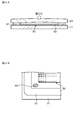
- 4A and 4B are diagrams illustrating a case where a gap difference in a region of a light emitting unit occurs depending on a ratio between a cell volume and a volume of a sealing liquid.
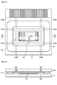
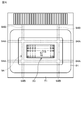
- FIG. 5A is a schematic plan view illustrating the panel structure of the display panel according to the first embodiment
- FIG. 5B is a cross-sectional view taken along line AA of FIG. 5A.
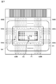
- FIG. 6 is a schematic plan view illustrating the panel structure of the display panel according to the second embodiment.
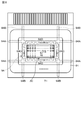
- FIG. 7 is a schematic plan view illustrating the panel structure of the display panel according to the third embodiment.
- FIG. 8 is a schematic plan view illustrating the panel structure of the display panel according to the fourth embodiment.
- FIG. 9 is a schematic plan view illustrating the panel structure of the display panel according to the fifth embodiment.
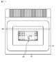
- FIG. 10 is a schematic plan view illustrating the panel structure of the display panel according to the sixth embodiment.
- FIG. 11 is a schematic plan view illustrating the panel structure of the display panel according to the seventh embodiment.
- FIG. 12 is a schematic plan view illustrating the panel structure of the display panel according to the eighth embodiment.
- FIG. 13 is a schematic plan view illustrating the panel structure of the display panel according to the ninth embodiment.
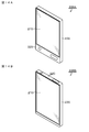
- FIG. 14A is an external view illustrating a first example of a smartphone according to Specific Example 1 of the electronic device of the present disclosure
- FIG. 14B is an external view illustrating a second example of the smartphone.
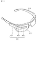
- FIG. 15 is an external view illustrating a head-mounted display according to Specific Example 2 of the electronic apparatus of the present disclosure.
- FIG. 16A is a front view of a digital still camera according to Specific Example 3 of the electronic device of the present disclosure
- FIG. 16B is a rear view of the digital still camera.
- Example 2 (Modification of Example 1: Example in which a part of the recess extends to the end face of the substrate) 3-3.
- Third Embodiment (Modification of First Embodiment: An example in which a plurality of recesses are provided around the light emitting unit) 3-4.
- Embodiment 4 (Modification of Embodiment 3: Example in which a plurality of recesses are provided inside a rectangular annular recess) 3-5.
- Example 5 (Modification of Example 3: Example in which a plurality of slot-shaped concave portions are provided around a light emitting unit) 3-6.
- Example 6 (Modification of Example 1: Example in which two concave portions are formed along the row direction around the area of the light emitting section) 3-7.
- Example 7 (Modification of Example 1: Example in which one concave portion is formed along the row direction around the area of the light emitting section) 3-8.
- Example 8 (an example in which a concave portion is formed in a hook shape at a portion corresponding to a corner portion of a seal portion) 3-9.
- Example 9 (an example in which a concave portion is formed to cross two sides of a corner portion of a seal portion) 4.
- Electronic device of the present disclosure 5-1. Specific example 1 (example of smartphone) 5-2.
- Example 2 (Example of head mounted display) 5-3.
- Example 3 (Example of digital still camera) 6. Configurations that the present disclosure can take
- one of the substrates having the concave portion may be configured to be the second substrate. Further, when the concave portion is formed in a rectangular ring shape in plan view around the region of the light emitting portion, and when the seal portion is formed outside the concave portion in a rectangular ring shape in plan view, a part of the concave portion is viewed in plan view. It is possible to adopt a configuration formed in a state of intersecting with the seal portion.
- a part of the concave portion may have a length that exceeds the width of the seal portion.
- a configuration extending to the end face can be adopted.
- a configuration may be such that a plurality of recesses are formed along each side of the rectangular annular seal portion.
- a configuration may be adopted in which a plurality of concave portions are formed outside or inside the rectangular annular concave portion.
- the concave portion includes a plurality of slot-shaped concave portions formed on the rectangular annular seal portion along the seal portion.
- at least one light emitting unit may be formed along the row direction of the matrix arrangement of the light emitting units so as to intersect with the seal unit in a plan view.
- the concave portion corresponds to the corner portion of the rectangular ring-shaped seal portion. It may be configured such that it is formed in a hook shape or in a state of crossing two sides of a corner at a portion to be bent.
- the display device includes a light emitting unit in which a plurality of sub-pixels include an organic EL element using electroluminescence (EL) of an organic material.
- EL electroluminescence
- Organic EL display device having a (light emitting element). That is, in the organic EL display device, each of the organic EL elements forms a sub-pixel.
- the organic EL element is a so-called current-driven electro-optical element whose emission luminance changes in accordance with the value of a current flowing through the device.
- the organic EL display device can be used, for example, as a monitor device constituting a personal computer, a video camera, a digital still camera, a television receiver, a mobile phone, a PDA (Personal Digital Assistant, a portable information terminal), a game, and the like. It can be used as a monitoring device built into equipment.
- the present invention can be applied to an electronic view finder (Electronic View Finder: EVF) or a head mounted display (HMD).
- EVF Electronic View Finder
- HMD head mounted display
- other examples include lighting devices including a backlight device for a liquid crystal display device and a planar light source device.
- the organic layer serving as the light emitting functional layer includes a light emitting layer (for example, a light emitting layer made of an organic light emitting material).
- the organic layer includes, for example, a laminated structure of a hole transport layer, a light emitting layer, and an electron transport layer, a laminated structure of a hole transport layer and a light emitting layer serving as an electron transport layer, and a hole injection layer.
- the organic layer may have a two-stage tandem structure in which a first tandem unit, a connection layer, and a second tandem unit are stacked. Further, it may have a tandem structure of three or more layers in which three or more tandem units are stacked. In these cases, an organic layer that emits white light as a whole can be obtained by changing the emission color to red, green, and blue for each tandem unit.
- a physical vapor deposition method such as a vacuum evaporation method
- a printing method such as a screen printing method or an inkjet printing method
- PVD method physical vapor deposition method
- a printing method such as a screen printing method or an inkjet printing method
- a laser transfer method in which an organic layer is separated from the laser absorbing layer by irradiating the structure with laser light and the organic layer is transferred, and various coating methods can be exemplified.
- an organic layer can be obtained by depositing a material that has passed through an opening provided in the metal mask. It may be formed over the entire surface without patterning.
- the display device is an active matrix display device in which a current flowing through an electro-optical element is controlled by an active element provided in the same pixel circuit as the electro-optical element, for example, an insulated gate field-effect transistor.
- an insulated gate field effect transistor typically, a MOS (Metal Oxide Semiconductor) transistor and a TFT (Thin Film Transistor) can be exemplified.
- an active matrix organic EL display device using an organic EL element as an example of a current-driven electro-optical element as a light emitting portion (light emitting element) of a pixel circuit will be described as an example. It shall be.
- the “pixel circuit” may be simply referred to as “pixel”.
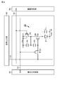
- FIG. 1 is a system configuration diagram illustrating an outline of a basic configuration of an active matrix organic EL display device that is a display device to which the technology of the present disclosure is applied.
- an active matrix organic EL display device 10 to which the technology of the present disclosure is applied has a pixel array in which a plurality of pixels 20 including organic EL elements are two-dimensionally arranged in a matrix.
- the configuration includes a unit 30 and a peripheral circuit (peripheral driving unit) arranged in a peripheral region of the pixel array unit 30.
- the peripheral circuit of the pixel region includes, for example, the writing scanning unit 40, the driving scanning unit 50, and the signal output unit 60 mounted on the same display panel 70 as the pixel array unit 30, and each pixel of the pixel array unit 30 20 is driven. Note that it is also possible to adopt a configuration in which some or all of the writing scanning unit 40, the driving scanning unit 50, and the signal output unit 60 are provided outside the display panel 70.
- an insulating transparent substrate such as a glass substrate or a semiconductor substrate such as a silicon substrate can be used.
- An organic EL display device using a semiconductor substrate such as a silicon substrate as a substrate of the display panel 70 is called a so-called micro display (small display), and is used as an electronic viewfinder of a digital still camera, a display unit of a head mounted display, and the like. It is suitable for use.
- the organic EL display device 10 may be configured to support monochrome (black and white) display, or may be configured to support color display.
- one pixel (unit pixel / pixel) serving as a unit for forming a color image includes a plurality of sub-pixels (sub-pixels).
- each of the sub-pixels corresponds to the pixel 20 in FIG. More specifically, in a display device that supports color display, one pixel includes, for example, a sub-pixel that emits red (Red; R) light, a sub-pixel that emits green (Green; G) light, and a blue (Blue). B) three sub-pixels that emit light.
- one pixel is not limited to a combination of sub-pixels of three primary colors of R, G, and B, and one pixel or a plurality of sub-pixels is added to the sub-pixels of three primary colors to form one pixel. It is also possible to configure. More specifically, for example, at least one pixel is formed by adding a sub-pixel that emits white (W) light to improve luminance, or at least emits complementary color light to expand the color reproduction range. It is also possible to form one pixel by adding one sub-pixel.
- W white
- the scanning lines 31 (31 1 to 31 m ) and the driving lines 32 (32) are arranged along the first direction (row direction / horizontal direction) with respect to the arrangement of the pixels 20 in m rows and n columns. 1 to 32 m ) are wired for each pixel row. Further, signal lines 33 (33 1 to 33 n ) are arranged for each pixel column along the second direction (column direction / vertical direction) with respect to the arrangement of the pixels 20 in m rows and n columns.
- the scanning lines 31 1 to 31 m are respectively connected to the output ends of the corresponding rows of the writing scanning unit 40.
- the drive lines 32 1 to 32 m are connected to output ends of the corresponding rows of the drive scanning unit 50, respectively.
- the signal lines 33 1 to 33 n are connected to the output ends of the corresponding columns of the signal output unit 60, respectively.
- the writing scanning unit 40 is configured by a shift register circuit and the like. When writing the signal voltage of the video signal to each pixel 20 of the pixel array unit 30, the writing scanning unit 40 writes the scanning signal WS (WS 1 to WS m ) to the scanning line 31 (31 1 to 31 m ). Are sequentially supplied, so-called line-sequential scanning is performed in which the pixels 20 of the pixel array unit 30 are sequentially scanned in row units.
- the drive scanning unit 50 is configured by a shift register circuit and the like, like the writing scanning unit 40.
- the drive scanning unit 50 supplies the light emission control signals DS (DS 1 to DS m ) to the drive lines 32 (32 1 to 32 m ) in synchronization with the line-sequential scanning by the writing scanning unit 40, thereby forming the pixels.
- the light emission / non-light emission (extinction) of the light emitting element 20 is controlled.
- the signal output unit 60 includes a signal voltage (hereinafter, sometimes simply referred to as “signal voltage”) V sig of a video signal corresponding to luminance information supplied from a signal supply source (not shown) and a reference voltage V ofs. And are selectively output.
- the reference voltage V ofs is a voltage corresponding to a reference voltage of the signal voltage V sig of the video signal (for example, a voltage corresponding to a black level of the video signal), or a voltage in the vicinity thereof.
- the reference voltage V ofs is used as an initialization voltage when performing a correction operation.
- the signal voltage V sig / reference voltage V ofs alternatively output from the signal output unit 60 is written and scanned to each pixel 20 of the pixel array unit 30 via the signal line 33 (33 1 to 33 n ).
- the data is written in the unit of the pixel row selected by the line sequential scanning by the unit 40. That is, the signal output unit 60 employs a driving mode of line-sequential writing in which the signal voltage V sig is written in pixel row (line) units.
- FIG. 2 is a circuit diagram showing an example of a circuit configuration of a pixel (pixel circuit) in the active matrix organic EL display device 10.
- the light emitting section of the pixel 20 is composed of the organic EL element 21.
- the organic EL element 21 is an example of a current-driven electro-optical element whose emission luminance changes according to the value of a current flowing through the device.
- the pixel 20 includes an organic EL element 21 and a driving circuit (pixel driving circuit) that drives the organic EL element 21 by passing a current through the organic EL element 21.
- a cathode electrode is connected to a common power supply line 34 commonly wired to all the pixels 20.
- C el is the equivalent capacitance of the organic EL element 21.
- the driving circuit for driving the organic EL element 21 includes a driving transistor 22, a sampling transistor 23, a light emission control transistor 24, a storage capacitor 25, and an auxiliary capacitor 26.
- the organic EL element 21 and its driving circuit are formed not on an insulator such as glass but on a semiconductor such as silicon, and a P-channel transistor is used as the driving transistor 22. Has been adopted.
- the driving transistor 22, the sampling transistor 23, and the light emission control transistor 24 have four terminals of source / gate / drain / back gate instead of three terminals of source / gate / drain.
- the power supply voltage Vdd is applied to the back gate.
- sampling transistor 23 and the light emission control transistor 24 are switching transistors that function as switching elements, they are not limited to P-channel transistors. Therefore, the sampling transistor 23 and the light emission control transistor 24 may be N-channel transistors or may have a structure in which P-channel transistors and N-channel transistors are mixed.
- the sampling transistor 23 writes the signal voltage V sig of the video signal supplied from the signal output unit 60 through the signal line 33 to the storage capacitor 25 by sampling.
- the light emission control transistor 24 is connected between the node of the power supply voltage Vdd and the source electrode of the drive transistor 22, and controls light emission / non-light emission of the organic EL element 21 under driving by the light emission control signal DS.
- the storage capacitor 25 is connected between the gate electrode and the source electrode of the drive transistor 22. This storage capacitor 25 holds the signal voltage V sig of the video signal written by sampling by the sampling transistor 23.
- the drive transistor 22 drives the organic EL element 21 by flowing a drive current according to the holding voltage of the storage capacitor 25 to the organic EL element 21.
- the storage capacitor 26 is connected between the source electrode of the driving transistor 22 and a node of a fixed potential, for example, a node of the power supply voltage Vdd .
- the auxiliary capacitor 26 suppresses the source potential of the drive transistor 22 from fluctuating when the signal voltage V sig of the video signal is written, and also reduces the gate-source voltage V gs of the drive transistor 22 The operation of setting the threshold voltage Vth is performed.
- the structure (panel structure) of the display panel 70 on which the pixel array section 30 and its peripheral circuits are formed is basically the same as the first substrate on which the light emitting section is formed.
- the first substrate is described as a support substrate
- the second substrate is described as a counter substrate.
- the panel structure of the display panel 70 includes a so-called top emission type panel structure in which light is extracted from the side opposite to the support substrate, and a so-called bottom emission type panel structure in which light is extracted from the support substrate side.
- the technology of the present disclosure can be applied to any of a panel structure of a top emission type panel structure and a panel structure of a bottom emission type panel structure.
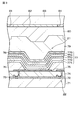
- FIG. 3 is a cross-sectional view illustrating an example of a panel structure for one pixel of the display panel 70.
- the panel structure of the display panel 70 exemplified here has a structure in which any one of R (red), G (green), and B (blue) color light is applied to the panel by a combination of a white organic EL element that emits white light and a color filter.
- This is a top emission type panel structure that is emitted from the upper surface (the surface opposite to the support substrate 71).
- the area on the support substrate 71 includes an effective pixel area (display area) in which a plurality of pixels 20 are arranged in a matrix, and a peripheral area located on the periphery (outer edge / outer periphery) of the effective pixel area.
- a pixel driving circuit including a driving transistor 22, a sampling transistor 23, a light emission control transistor 24, a storage capacitor 25, and an auxiliary capacitor 26 is provided.
- a peripheral circuit including a writing scanning unit 40, a driving scanning unit 50, a signal output unit 60, and the like is provided.
- a circuit layer 72 including these circuits is formed on the substrate 71.
- the display panel 70 includes, for example, an inorganic insulating layer 73, a base insulating layer 74, an anode electrode 75, an organic insulating layer 76, an organic layer 77, a cathode electrode 78, an organic protective layer 79, and a filler layer on the circuit layer 72.
- An adhesive layer 80 and a black matrix layer 81 have a laminated structure in which the layers are laminated in this order. Note that a color filter 82 is provided in the same layer as the black matrix layer 81 for each pixel. Further, an opposing substrate 83 is bonded on the laminated structure, and the opposing substrate 83 seals the laminated structure.
- the anode electrode 75, the organic layer 77, and the cathode electrode 78 have a laminated structure forming the organic EL element 21 that emits white light.
- the anode electrode 75 is provided as an independent electrode for each pixel 20 of each color in the effective pixel region.
- the cathode electrode 78 is formed of a transparent electrode, and is provided as an electrode common to each pixel 20 in the effective pixel area.
- the organic layer 77 has a stacked structure in which a hole injection layer 771, a hole transport layer 772, a light emitting layer 773, an electron transport layer 774, and an electron injection layer 775 are stacked in this order from the anode electrode 75 side. . Of these layers, layers other than the light-emitting layer 773 may be provided as needed.
- the hole injection layer 771 is provided to increase hole injection efficiency and prevent leakage.
- the hole transport layer 772 is for increasing the efficiency of transporting holes to the light emitting layer 773. In the light-emitting layer 773, recombination of electrons and holes occurs when an electric field is applied, and light is generated.
- the electron transport layer 774 is for increasing the efficiency of transporting electrons to the light emitting layer 773.
- the electron injection layer 775 is for increasing electron injection efficiency.
- the base insulating layer 74 is provided so as to cover a circuit portion (a pixel driving circuit, a peripheral circuit, and the like) formed on the support substrate 71.
- the configuration is such that the organic EL element 21 is formed thereon.
- An anode electrode 75 is provided as a lower electrode in pixel units below the organic EL element 21, and a cathode electrode 78 is provided as an upper electrode on the organic EL element 21 in common for all pixels.
- the display panel 70 is formed by bonding the support substrate 71 as the first substrate and the counter substrate 83 as the second substrate. More specifically, as described later, the display panel 70 includes a support substrate 71 and a counter substrate 83 that are bonded to each other outside a region of the light emitting unit (the pixel array unit 30) by a seal unit, and are surrounded by the seal unit.
- the panel structure is such that the region including the light emitting portion is filled with the filling liquid.
- the gap between the support substrate 71 and the counter substrate 83 needs to be stable in the area of the light emitting section.
- the area of the light emitting section surrounded by the seal section hereinafter, referred to as “cell volume”
- the volume of the sealing liquid filled in the area are determined by the ratio of the area of the light emitting section to the area of the light emitting section. A gap difference may occur.
- the gap difference in the region of the light emitting section occurs depending on the ratio of the cell volume to the volume of the sealing liquid
- the filling liquid 92 is filled in the region including the light emitting part surrounded by the seal part 91 and the volume of the filling liquid 92 becomes larger than the cell volume, as shown in FIG. 83 will have a convex bulge.
- the volume of the sealing liquid 92 becomes smaller than the cell volume, as shown in FIG. 4B, a bubble-like void 93 is generated in the region including the light emitting unit (the pixel array unit 30). become. From such a viewpoint, it is extremely important to strictly control the relationship between the cell volume and the volume of the sealed liquid 92.
- the support substrate 71 On at least one of the substrates 83, a concave portion is formed outside the region of the light emitting portion (pixel array portion 30), and a seal portion is formed outside the concave portion.
- the other substrate on which the concave portion is formed is the opposite substrate 83.
- the seal portion is formed in a rectangular ring shape around the light emitting portion region (pixel array portion 30), and a part of the concave portion intersects the seal portion and has a length exceeding the width of the seal portion. It can be configured.
- the annular shape of the seal portion is not limited to a rectangular shape.
- the recess is not necessarily limited to a configuration in which a part thereof intersects the seal portion or a configuration having a length exceeding the width of the seal portion.
- At least one of the support substrate 71 and the counter substrate 83 has a concave portion formed outside the light emitting region and a seal portion formed outside the concave portion.
- the gap between the support substrate 71 and the counter substrate 83 can be made uniform over the entire area of the light emitting section without providing a spacer in the display area.
- the concave portion is formed in a portion outside the region of the light emitting section, the extra filling liquid can flow into the concave portion, so that the relationship between the cell volume and the volume of the filling liquid is reduced. Can be strictly controlled.
- the gap between the support substrate 71 and the counter substrate 83 can be made uniform over the entire area of the light emitting section.
- the concave portion can also serve as a bubble eliminator that allows the bubble-like void to flow.
- the gap between the supporting substrate 71 and the opposing substrate 83 can be made uniform by the action of the concave portion, and the concave portion can also serve to remove air bubbles. Accordingly, the gap between the support substrate 71 and the counter substrate 83 can be made uniform without providing a spacer or the like in the display region, so that the luminous efficiency does not decrease due to the presence of the spacer or the like. , And high quality image quality can be provided.
- specific examples of the embodiment of the present disclosure will be described.
- the first embodiment is an example of a basic shape of a concave portion formed in a portion outside a region of a light emitting unit (pixel array unit 30).
- FIG. 5A is a schematic plan view of the panel structure of the display panel 70 according to the first embodiment, and FIG. 5B is a cross-sectional view taken along line AA of FIG. 5A.
- the support substrate 71 is made of a silicon substrate, a glass substrate, a quartz substrate, a plastic substrate, or the like.
- a pixel array unit 30 in which light emitting units (organic EL elements 21) are two-dimensionally arranged in a matrix is formed, and although not shown, a driving circuit for the light emitting unit, A wiring portion for electrically connecting the light emitting portion and the drive circuit is provided.
- the opposing substrate 83 (not shown in FIG. 5A) is made of a translucent material such as quartz, glass, or plastic.
- a rectangular annular concave portion 94 having a rounded corner in a plan view is formed in a region outside the pixel array unit 30 in the counter substrate 83.
- the formation of the concave portion 94 can be performed by etching or dicing.
- the concave portion 94 formed in the counter substrate 83 is shown by a broken line. The same applies to each embodiment described later.
- the support substrate 71 and the counter substrate 83 are bonded to the outside of the concave portion 94 via a sealing portion 91 made of a sealing material similarly formed in a rectangular shape in plan view. Then, a sealing liquid 92 is sealed in a cell formed by the support substrate 71, the counter substrate 83, and the seal portion 91. After the sealing liquid 92 is sealed, the sealing liquid 92 is completely cured by UV irradiation or heating.
- a method for filling the filling liquid 92 may be an inlet method or an ODF (One Drop Fill) method.
- the injection port method is a method in which after the support substrate 71 and the opposing substrate 83 are bonded to each other, a sealing liquid 92 is sealed through an injection hole formed in the seal portion 91.
- the ODF method is a method in which a sealing liquid 92 is dropped on the support substrate 71 or the counter substrate 83 before the support substrate 71 and the counter substrate 83 are bonded, and then the support substrate 71 and the counter substrate 83 are bonded.
- the concave portion 94 is formed in a region between the pixel array portion 30 and the seal portion 91 on the counter substrate 83, for example, in a rectangular ring shape in plan view.
- the rectangular annular concave portion 94 has, at four corners, extended portions 94A and 94B that partially extend along the row direction and the column direction of the pixel array section 30.
- the extended portions 94A and 94B, which are part of the concave portion 94, are formed so as to intersect with the seal portion 91 in plan view, and have a length exceeding the width of the seal portion 91.
- the concave portion 94 is formed in the portion of the counter substrate 83 outside the pixel array portion 30, so that the extra filling is performed. Since the liquid 92 can flow into the concave portion 94, the relationship between the cell volume and the volume of the sealed liquid can be strictly controlled.
- the concave portion 94 has the elongated portions 94A and 94B having a length exceeding the width of the seal portion 91 at the four corners of the rectangular annular shape, the effect that the extra filled liquid 92 can flow is obtained. large.
- the extending portions 94A and 94B intersecting the seal portion 91 in a plan view are provided at four corners of a rectangular ring, but the invention is not limited to the four corners.
- the relationship between the cell volume and the volume of the sealing liquid can be strictly controlled by the action of the concave portion 94, so that the gap between the support substrate 71 and the counter substrate 83 can be made uniform over the entire area of the light emitting section. can do.
- the concave portion 94 can also serve as a bubble eliminator that allows the bubble-like space 93 to flow. . As a result, high quality image quality can be provided.
- the second embodiment is a modification of the first embodiment, and is an example in which a part of the concave portion extends to the end surface of the substrate.
- FIG. 6 is a schematic plan view of the panel structure of the display panel 70 according to the second embodiment.
- the panel structure of the display panel 70 according to the second embodiment is different from the panel structure of the display panel 70 according to the first embodiment in that the extending portions 94A and 94B, which are part of the concave portion 94, are the end surfaces of the counter substrate 83 (see FIG. 5B). It is configured to extend to Since a part of the concave portion 94 extends to the end face of the substrate in this manner, in addition to the same operation and effect as in the first embodiment, a plurality of chips are formed when the concave portion 94 is processed by, for example, dicing. There is an advantage that the concave portion 94 can be processed at a time between them.
- the third embodiment is a modification of the first embodiment, and is an example in which a plurality of recesses are provided around a region (pixel array unit 30) including a light emitting unit.
- FIG. 7 shows a schematic plan view of a panel structure of a display panel 70 according to the third embodiment.
- the panel structure of the display panel 70 according to the third embodiment is different from the panel structure of the display panel 70 according to the first embodiment in that a plurality of extending portions 94 ⁇ / b> A of the concave portion 94 are provided on the left and right of the pixel array portion 30.
- the upper and lower portions are provided with a plurality of extending portions 94B of the concave portion 94. That is, a plurality of extending portions 94A and extending portions 94B of the concave portion 94 are provided outside the rectangular annular concave portion 94 along each side of the rectangular annular seal portion 91.
- the plurality of extension portions 94A and the plurality of extension portions 94B are formed so as to intersect with the seal portion 91 in a plan view, and have a length exceeding the width of the seal portion 91.
- the sealing liquid 92 and the bubbles are provided. Since the gap 93) can efficiently flow into the recess 94, higher quality image quality can be provided.
- the fourth embodiment is a modification of the third embodiment, and is an example in which a plurality of recesses are provided inside a rectangular annular recess 94 in plan view.
- FIG. 8 is a schematic plan view of a panel structure of a display panel 70 according to the fourth embodiment.
- the panel structure of the display panel 70 according to the third embodiment is such that all of the plurality of extension portions 94A and the plurality of extension portions 94B intersect with the seal portion 91 in plan view outside the rectangular annular concave portion 94 in plan view. It is the structure formed by.
- the plurality of extension portions 94C and the extension portions 94D except for the extension portions 94A and 94B at the corners of the rectangular annular concave portion 94 are formed in a rectangular annular shape. The structure is formed inside the concave portion 94.
- the sealing liquid 92 and the bubbles are formed inside the rectangular annular concave portion 94 in a plan view. Since the gap 93) can efficiently flow into the concave portion 94, higher quality image quality can be provided.
- the fifth embodiment is a modification of the third embodiment, and is an example in which a plurality of slot-shaped concave portions corresponding to the extension portions 94A and 94B are provided around the light emitting unit region (pixel array unit 30).
- FIG. 9 shows a schematic plan view of a panel structure of a display panel 70 according to the fifth embodiment.
- the panel structure of the display panel 70 according to the fifth embodiment is different from the panel structure of the display panel 70 according to the third embodiment in that a plurality of elongated portions 94A and a plurality of elongated portions 94B corresponding to the plurality of elongated portions 94B are formed in the area of the light emitting portion.
- the plurality of slot-shaped concave portions 94 are formed on the rectangular annular seal portion 91 along the seal portion 91, and intersect with the seal portion 91 in plan view as in the case of the third embodiment. It is formed in a state, and has a length exceeding the width of the seal portion 91.
- the concave portion 94 corresponding to the corner of the seal portion 91 is formed radially with respect to the seal portion 91.
- the plurality of recesses 94 are arranged in a rectangular ring shape in plan view so as to surround the entire area of the light emitting unit.
- the sixth embodiment is a modification of the first embodiment, and is an example in which two concave portions are formed along the row direction around the area of the light emitting section.
- FIG. 10 shows a schematic plan view of a panel structure of a display panel 70 according to the sixth embodiment.
- the panel structure of the display panel 70 according to the sixth embodiment is such that two concave portions 94 are provided around the pixel array portion 30 (the region of the light emitting portion), more specifically, two concave portions 94 are provided above and below the pixel array portion 30. Are formed along the row direction.
- the two concave portions 94 are provided in a region between the pixel array portion 30 and the seal portion 91 above and below the pixel array portion 30, and are formed so as to intersect with the seal portion 91 in plan view. I have.
- the intersection of the two concave portions 94 with the seal portion 91 has a length exceeding the width of the seal portion 91.
- the concave portion 94 is formed in the region between the pixel array portion 30 and the seal portion 91 along the row direction, the excessively filled sealing liquid 92 flows into the concave portion 94, Since the gap between 71 and the opposing substrate 83 can be made uniform over the entire area of the light emitting section, high quality image can be provided. Moreover, since the recess 94 is only formed along the row direction, there is an advantage that the processing of the recess 94 is easy.
- two recesses 94 are extended to the end surface of the counter substrate 83 (see FIG. 5B). It is also possible to adopt a configuration in which it is located. When this configuration is adopted, there is an advantage that the concave portion 94 can be collectively processed between a plurality of chips when the concave portion 94 is processed by, for example, dicing, as in the case of the second embodiment.
- the seventh embodiment is a modification of the first embodiment, and is an example in which one concave portion is formed along the row direction around the area of the light emitting section.
- FIG. 11 is a schematic plan view of a panel structure of a display panel 70 according to the seventh embodiment.
- the concave portion 94 is formed around the pixel array section 30 (the area of the light emitting section), more specifically, the area above (or below) the pixel array section 30. And one of them is formed along the row direction of the pixel array section 30.
- One concave portion 94 is provided in a region between the pixel array portion 30 and the seal portion 91, and is formed so as to intersect with the seal portion 91 in plan view. The intersection of the single concave portion 94 with the seal portion 91 has a length exceeding the width of the seal portion 91.
- the effect of allowing the filled liquid 92 to flow into the recess 94 by the number of the recesses 94 is smaller. Although low, basically, the same operation and effect as those of the sixth embodiment can be obtained. Further, also in the panel structure of the display panel 70 according to the seventh embodiment, the technique of the second embodiment in which the concave portion 94 extends to the end face of the substrate can be applied.
- Example 8 is an example in which a concave portion is formed in a hook shape at a portion corresponding to a corner of a rectangular annular seal portion.
- FIG. 12 is a schematic plan view of a panel structure of a display panel 70 according to the eighth embodiment.
- the panel structure of the display panel 70 according to the eighth embodiment has a configuration in which the concave portion 94 is formed in a hook shape (L-shape / inverted L-shape) at a portion corresponding to a corner of the rectangular annular seal portion 91. ing.
- the bent hook portion is located in a region between the pixel array portion 30 and the seal portion 91, and the other extended portion is formed so as to intersect with the seal portion 91 in plan view. Further, it has a length exceeding the width of the seal portion 91.
- the hook-shaped concave portion 94 is formed at a position corresponding to the corner portion of the rectangular annular seal portion 91, particularly, the corner portion of the region between the pixel array portion 30 and the seal portion 91 is formed. Since the generated bubble-like space 93 (see FIG. 4B) can flow into the concave portion 94, it is possible to prevent image quality deterioration due to the bubble-like space 93.
- the hook-shaped recess 94 not only has a function of removing air bubbles, but also has a function of flowing an excessively filled sealed liquid 92.
- the hook-shaped concave portions 94 are formed at four corners of the seal portion 91 has been illustrated, but the present invention is not limited to the four corners.
- the ninth embodiment is an example in which a concave portion is formed so as to cross two sides of a corner of a rectangular annular seal portion.
- FIG. 13 is a schematic plan view of the panel structure of the display panel 70 according to the ninth embodiment.
- the panel structure of the display panel 70 according to the ninth embodiment has a configuration in which the concave portion 94 is formed so as to cross two sides of the corner of the rectangular annular seal portion 91.
- the middle portion is located in the region between the pixel array portion 30 and the seal portion 91, and the other portions are in a state of intersecting with the seal portion 91 in plan view. Formed, and has a length exceeding the width of the seal portion 91.
- the concave portion 94 in the crossed state has not only a function as a bubble elimination but also a function to flow an overfilled filling liquid 92.
- the case where the recessed portion 94 in the cross state is formed at the four corners of the seal portion 91 is illustrated, but the invention is not limited to the four corners.
- the technology of the present disclosure has been described based on the preferred embodiments, but the technology of the present disclosure is not limited to the embodiments.
- the configuration and structure of the display device described in the above embodiment are examples, and can be changed as appropriate.
- the technology of the present disclosure has been described by taking an organic EL device (display panel) as an example, but a display device other than the organic EL device, specifically, the first substrate and the second
- the technology of the present disclosure can be applied to all display devices having a panel structure in which a substrate is attached using a sealant.
- the concave portion 94 having the function of allowing the extra filling liquid 92 to flow in and the function of removing bubbles are formed in the counter substrate 83 which is the second substrate. It is also possible to form it on the supporting substrate 71 which is the substrate. However, considering that wiring and the like are formed on the supporting substrate 71, the substrate on which the concave portion 94 is formed is preferably the opposing substrate 83.
- Examples 1 to 9 were illustrated as examples of the shape of the concave portion 94.
- the present invention is not limited to these examples.
- the shape of the concave portion 94 is not limited as long as it is a concave portion 94 into which the gap 93 (see FIG. 4B) can flow.
- the display device of the present disclosure described above is a display unit (display device) of an electronic device in any field that displays a video signal input to the electronic device or a video signal generated in the electronic device as an image or a video.
- the electronic device include a television set, a notebook personal computer, a digital still camera, a portable terminal device such as a mobile phone, a head-mounted display, and the like. However, it is not limited to these.
- the technology of the present disclosure it is possible to provide a high-quality image by making the gap between the two substrates uniform. Then, by using the display device of the present disclosure as a display unit (display device) of electronic devices in all fields, a high-quality display image can be provided.
- a smartphone, a head-mounted display, and a digital still camera will be exemplified as specific examples of the electronic apparatus using the display device of the present disclosure.
- the specific examples illustrated here are merely examples, and the present invention is not limited to these specific examples.
- FIG. 14 illustrates an external view of a smartphone according to Specific Example 1 of the electronic device of the present disclosure.
- FIG. 14A is an external view showing a first example of a smartphone
- FIG. 14B is an external view showing a second example of a smartphone.
- the smartphone 100A of the first example and the smartphone 100B of the second example include the display unit 110 and the operation unit 120.
- the operation unit 120 is provided below the display unit 110 of the housing 130.
- the operation unit 120 is provided on the upper surface of the housing 130.
- the display device of the present disclosure can be used as the display unit 110 of the smartphones 100A and 100B. That is, the smartphones 100A and 100B according to the first specific example are manufactured by using the display device of the present disclosure as the display unit 110.
- FIG. 15 is an external view of a head mounted display according to a specific example 2 of the electronic apparatus of the present disclosure.
- the head-mounted display 200 has a transmission-type head-mounted display having a main body 201, an arm 202, and a lens barrel 203.
- the main body 201 is connected to the arm 202 and the glasses 210. Specifically, an end of the main body 201 in the long side direction is attached to the arm 202.
- One side of the side surface of the main body 201 is connected to the glasses 210 via a connection member (not shown). Note that the main body 201 may be directly mounted on the head of a human body.
- the main unit 201 incorporates a control board and a display unit for controlling the operation of the head mounted display 200.
- the arm 202 supports the lens barrel 203 with respect to the main body 201 by connecting the body 201 and the lens barrel 203. Specifically, the arm unit 202 fixes the lens barrel 203 to the main body 201 by being coupled to the end of the main body 201 and the end of the lens barrel 203.
- the arm unit 202 has a built-in signal line for communicating data relating to an image provided from the main unit 201 to the lens barrel 203.
- the lens barrel 203 projects image light provided from the main body 201 via the arm 202 through the lens 211 of the glasses 210 toward the eyes of the user wearing the head mounted display 200.
- the display device of the present disclosure can be used as a display unit built in the main body unit 201. That is, the head mounted display 200 according to the specific example 2 is manufactured by using the display device of the present disclosure as its display unit.
- FIG. 16 is an external view of a single-lens reflex digital still camera of the interchangeable lens type according to Example 3 of the electronic apparatus of the present disclosure.
- FIG. 16A is a front view of the digital still camera
- FIG. 16B is a rear view of the digital still camera.
- the interchangeable lens single-lens reflex digital still camera 300 has, for example, an interchangeable photographing lens unit (interchangeable lens) 312 on the front right side of a camera body (camera body) 311, and a photographer grips the front left side. And a grip portion 313 for performing the operation.
- a monitor 314 is provided substantially at the center of the rear surface of the camera body 311.
- a viewfinder (eyepiece window) 315 is provided above the monitor 314. By looking through the viewfinder 315, the photographer can visually recognize the light image of the subject guided by the photographing lens unit 312 and determine the composition.
- the display device of the present disclosure can be used as the viewfinder 315. That is, the interchangeable lens single-lens reflex digital camera 300 according to Example 3 is manufactured by using the display device of the present disclosure as the viewfinder 315.
- ⁇ A. Display device a first substrate on which a light emitting unit is formed, A second substrate opposed to the first substrate, and A sealing portion for bonding the first substrate and the second substrate, At least one of the first substrate and the second substrate has a concave portion formed at a portion outside a region of the light emitting portion, The seal portion is formed outside the concave portion, Display device.
- One of the substrates is a second substrate, The display device according to the above [A-1].
- the concave portion is formed in a rectangular ring shape in plan view around the region of the light emitting portion,
- the seal portion is formed in a rectangular ring shape in a plan view outside the concave portion, Part of the concave portion is formed in a state crossing the seal portion in plan view,
- [A-4] a part of the concave portion has a length exceeding the width of the seal portion; The display device according to the above [A-3].
- Part of the concave portion extends to the end surface of the substrate.
- a plurality of recesses are formed along each side of the rectangular annular seal portion.
- the display device according to the above [A-3].
- [A-7] A part of the concave portion is formed outside the rectangular annular concave portion.
- the display device according to the above [A-6].
- [A-8] Part of the concave portion is formed inside the rectangular annular concave portion.
- the display device according to the above [A-6].
- [A-9] The concave portion includes a plurality of slot-shaped concave portions formed on the rectangular annular seal portion along the seal portion.
- the display device according to any one of [A-3] to [A-5].
- [A-10] At least one concave portion is formed along the row direction of the matrix arrangement of the light emitting portions so as to intersect with the seal portion in plan view.
- the display device according to the above [A-1] or [A-2].
- the seal portion is formed in a rectangular ring shape in plan view, The recess is formed in a hook shape at a portion corresponding to a corner of the rectangular annular seal portion.
- [A-12] The seal portion is formed in a rectangular ring shape in plan view, The recess is formed at a position corresponding to the corner of the rectangular annular seal portion in a state of crossing two sides of the corner.
- [A-13] The light emitting section is formed of an organic electroluminescence element. The display device according to any of [A-1] to [A-12].
- ⁇ B. Electronics [B-1] a first substrate on which a light emitting unit is formed, A second substrate opposed to the first substrate, and A sealing portion for bonding the first substrate and the second substrate, At least one of the first substrate and the second substrate has a concave portion formed at a portion outside a region of the light emitting portion, The seal portion is formed outside the concave portion, An electronic device having a display device. [B-2] One of the substrates is a second substrate, The electronic device according to the above [B-1].
- the concave portion is formed in a rectangular ring shape in plan view around the region of the light emitting portion,
- the seal portion is formed in a rectangular ring shape in a plan view outside the concave portion, Part of the concave portion is formed in a state crossing the seal portion in plan view,
- Part of the concave portion has a length exceeding the width of the seal portion.
- Part of the concave portion extends to the end surface of the substrate.
- a plurality of recesses are formed along each side of the rectangular annular seal portion.
- [B-7] A part of the concave portion is formed outside the rectangular annular concave portion.
- Part of the concave portion is formed inside the rectangular annular concave portion.
- [B-9] The recess includes a plurality of slot-shaped recesses formed on the rectangular annular seal portion along the seal portion.
- [B-10] At least one concave portion is formed along the row direction of the matrix arrangement of the light emitting portions so as to intersect with the seal portion in plan view.
- the seal portion is formed in a rectangular ring shape in plan view.
- the recess is formed in a hook shape at a portion corresponding to a corner of the rectangular annular seal portion.
- the seal portion is formed in a rectangular ring shape in plan view.
- the recess is formed at a position corresponding to the corner of the rectangular annular seal portion in a state of crossing two sides of the corner.
- the light emitting section is composed of an organic electroluminescence element.
Landscapes
- Physics & Mathematics (AREA)
- Engineering & Computer Science (AREA)
- Microelectronics & Electronic Packaging (AREA)
- Optics & Photonics (AREA)
- General Physics & Mathematics (AREA)
- Theoretical Computer Science (AREA)
- Geometry (AREA)
- Electroluminescent Light Sources (AREA)
- Devices For Indicating Variable Information By Combining Individual Elements (AREA)
Abstract
本開示の表示装置は、発光部が形成された第1の基板、第1の基板と対向配置された第2の基板、及び、第1の基板と第2の基板とを貼り合わせるシール部を備える。そして第1の基板及び第2の基板の少なくとも一方の基板はは、発光部の領域よりも外側の部位に形成された凹部を有し、シール部は、凹部の外側に形成されている。また、本開示の電子機器は、上記の構成の表示装置を有する。
Description
本開示は、表示装置及び電子機器に関する。
近年の表示装置は、フラットパネル型(平面型)の表示装置が主流である。フラットパネル型の表示装置のパネル構造は、基本的に、発光部が形成された基板と、当該基板と対向配置された基板とを貼り合わせた構造となっている。
このようなパネル構造の表示装置において、良質な画質を得るためには、貼り合わせた2つの基板間のギャップが、発光部の領域内で安定している必要がある。そのため、従来は、表示領域内(発光部の領域内)にスペーサを配置し、2つの基板間のギャップの一定化を図るようにしている(例えば、特許文献1参照)。
上記の特許文献1に記載の従来技術では、表示領域内にスペーサを配置することで、ギャップの一定化を図るようにしているが、表示領域内にスペーサが存在することによって発光効率が低下するという問題がある。
そこで、本開示は、表示領域内にスペーサを設けることなく、2つの基板間のギャップの一定化を図ることができる表示装置、及び、当該表示装置を有する電子機器を提供することを目的とする。
上記の目的を達成するための本開示の表示装置は、
発光部が形成された第1の基板、
第1の基板と対向配置された第2の基板、及び、
第1の基板と第2の基板とを貼り合わせるシール部を備えている。そして、
第1の基板及び第2の基板の少なくとも一方の基板は、発光部の領域よりも外側の部位に形成された凹部を有し、
シール部は、凹部の外側に形成されている。
発光部が形成された第1の基板、
第1の基板と対向配置された第2の基板、及び、
第1の基板と第2の基板とを貼り合わせるシール部を備えている。そして、
第1の基板及び第2の基板の少なくとも一方の基板は、発光部の領域よりも外側の部位に形成された凹部を有し、
シール部は、凹部の外側に形成されている。
また、上記の目的を達成するための本開示の電子機器は、上記の構成の第1の基板、第2の基板、及び、シール部を備える表示装置を、表示部(表示装置)として有する。
以下、本開示の技術を実施するための形態(以下、「実施形態」と記述する)について図面を用いて詳細に説明する。本開示の技術は実施形態に限定されるものではない。以下の説明において、同一要素又は同一機能を有する要素には同一符号を用いることとし、重複する説明は省略する。尚、説明は以下の順序で行う。
1.本開示の表示装置及び電子機器、全般に関する説明
2.本開示の技術が適用されるアクティブマトリクス型表示装置
2-1.システム構成
2-2.画素回路
2-3.基本的な画素構造
3.本開示の実施形態
3-1.実施例1(発光部の領域よりも外側に形成される凹部の基本形の例)
3-2.実施例2(実施例1の変形例:凹部の一部を基板端面まで延在させた例)
3-3.実施例3(実施例1の変形例:凹部の一部を発光部の周りに複数設けた例)
3-4.実施例4(実施例3の変形例:凹部の一部を、矩形環状の凹部の内側に複数設けた例)
3-5.実施例5(実施例3の変形例:スロット状の凹部を発光部の周りに複数設けた例)
3-6.実施例6(実施例1の変形例:凹部を発光部の領域の周りに、行方向に沿って2本形成した例)
3-7.実施例7(実施例1の変形例:凹部を発光部の領域の周りに、行方向に沿って1本形成した例)
3-8.実施例8(シール部の角部に対応する部位に凹部を鉤型に形成した例)
3-9.実施例9(シール部の角部の2辺に対し凹部をクロスして形成した例)
4.変形例
5.本開示の電子機器
5-1.具体例1(スマートフォンの例)
5-2.具体例2(ヘッドマウントディスプレイの例)
5-3.具体例3(デジタルスチルカメラの例)
6.本開示がとることができる構成
1.本開示の表示装置及び電子機器、全般に関する説明
2.本開示の技術が適用されるアクティブマトリクス型表示装置
2-1.システム構成
2-2.画素回路
2-3.基本的な画素構造
3.本開示の実施形態
3-1.実施例1(発光部の領域よりも外側に形成される凹部の基本形の例)
3-2.実施例2(実施例1の変形例:凹部の一部を基板端面まで延在させた例)
3-3.実施例3(実施例1の変形例:凹部の一部を発光部の周りに複数設けた例)
3-4.実施例4(実施例3の変形例:凹部の一部を、矩形環状の凹部の内側に複数設けた例)
3-5.実施例5(実施例3の変形例:スロット状の凹部を発光部の周りに複数設けた例)
3-6.実施例6(実施例1の変形例:凹部を発光部の領域の周りに、行方向に沿って2本形成した例)
3-7.実施例7(実施例1の変形例:凹部を発光部の領域の周りに、行方向に沿って1本形成した例)
3-8.実施例8(シール部の角部に対応する部位に凹部を鉤型に形成した例)
3-9.実施例9(シール部の角部の2辺に対し凹部をクロスして形成した例)
4.変形例
5.本開示の電子機器
5-1.具体例1(スマートフォンの例)
5-2.具体例2(ヘッドマウントディスプレイの例)
5-3.具体例3(デジタルスチルカメラの例)
6.本開示がとることができる構成
<本開示の表示装置及び電子機器、全般に関する説明>
本開示の表示装置及び電子機器にあっては、凹部を有する一方の基板について、第2の基板である構成とすることができる。また、凹部が発光部の領域の周りに、平面視で矩形環状に形成され、シール部が凹部の外側に、平面視で矩形環状に形成されているとき、凹部の一部について、平面視でシール部と交差した状態で形成されている構成とすることができる。
本開示の表示装置及び電子機器にあっては、凹部を有する一方の基板について、第2の基板である構成とすることができる。また、凹部が発光部の領域の周りに、平面視で矩形環状に形成され、シール部が凹部の外側に、平面視で矩形環状に形成されているとき、凹部の一部について、平面視でシール部と交差した状態で形成されている構成とすることができる。
上述した好ましい構成を含む本開示の表示装置及び電子機器にあっては、凹部の一部について、シール部の幅を超える長さを有している構成とすることができるし、更に、基板の端面まで延在している構成とすることができる。
また、上述した好ましい構成を含む本開示の表示装置及び電子機器にあっては、凹部の一部について、矩形環状のシール部の各辺に沿って複数形成されている構成とすることができる。このとき、凹部の複数の一部について、矩形環状の凹部の外側又は内側に形成されている構成とすることができる。
あるいは又、上述した好ましい構成を含む本開示の表示装置及び電子機器にあっては、凹部について、矩形環状のシール部上に当該シール部に沿って形成されたスロット状の複数の凹部から成る、あるいは、発光部の行列状配列の行方向に沿って、平面視でシール部と交差した状態で少なくとも1本形成されている構成とすることができる。
あるいは又、上述した好ましい構成を含む本開示の表示装置及び電子機器にあっては、シール部が平面視で矩形環状に形成されているとき、凹部について、矩形環状のシール部の角部に対応する部位に、鉤型に形成されている、あるいは、角部の2辺に対してクロスする状態で形成されている構成とすることができる。
上述した好ましい構成を含む本開示の表示装置及び電子機器にあっては、表示装置を、複数の副画素が、有機材料のエレクトロルミネッセンス(EL:Electro Luminescence)を利用した有機EL素子から成る発光部(発光素子)を有する有機EL表示装置の構成とすることができる。すなわち、有機EL表示装置にあっては、有機EL素子のそれぞれによって副画素が構成される。有機EL素子は、デバイスに流れる電流値に応じて発光輝度が変化する、所謂、電流駆動型の電気光学素子である。
有機EL表示装置は、例えば、パーソナルコンピュータやビデオカメラ、デジタルスチルカメラを構成するモニター装置として使用することができるし、テレビジョン受像機や携帯電話機、PDA(Personal Digital Assistant,携帯情報端末)、ゲーム機器に組み込まれたモニター装置として使用することができる。あるいは又、電子ビューファインダー(Electronic View Finder:EVF)や頭部装着型ディスプレイ(Head Mounted Display:HMD)に適用することができる。あるいは又、その他、液晶表示装置用のバックライト装置や面状光源装置を含む照明装置を挙げることができる。
有機EL素子において、発光機能層である有機層は、発光層(例えば、有機発光材料から成る発光層)を備えている。この有機層は、具体的には、例えば、正孔輸送層と発光層と電子輸送層との積層構造、正孔輸送層と電子輸送層を兼ねた発光層との積層構造、正孔注入層と正孔輸送層と発光層と電子輸送層と電子注入層との積層構造等から構成することができる。また、これらの積層構造等をタンデムユニットとする場合、有機層は、第1のタンデムユニット、接続層、及び、第2のタンデムユニットが積層された2段のタンデム構造を有していてもよく、更には、3つ以上のタンデムユニットが積層された3段以上のタンデム構造を有していてもよい。これらの場合、発光色を赤色、緑色、青色と各タンデムユニットで変えることで、全体として白色を発光する有機層を得ることができる。
有機層の形成方法として、真空蒸着法等の物理的気相成長法(PVD法);スクリーン印刷法やインクジェット印刷法といった印刷法;転写用基板上に形成されたレーザ吸収層と有機層の積層構造に対してレーザ光を照射することでレーザ吸収層上の有機層を分離して、有機層を転写するといったレーザ転写法、各種の塗布法を例示することができる。有機層を真空蒸着法に基づき形成する場合、例えば、所謂メタルマスクを用い、当該メタルマスクに設けられた開口を通過した材料を堆積させることによって有機層を得ることができるし、有機層を、パターニングすること無く、全面に形成してもよい。
<本開示の技術が適用される表示装置>
本開示の表示装置は、電気光学素子に流れる電流を、当該電気光学素子と同じ画素回路内に設けた能動素子、例えば絶縁ゲート型電界効果トランジスタによって制御するアクティブマトリクス型表示装置である。絶縁ゲート型電界効果トランジスタとしては、典型的には、MOS(Metal Oxide Semiconductor)トランジスタやTFT(Thin Film Transistor;薄膜トランジスタ)を例示することができる。
本開示の表示装置は、電気光学素子に流れる電流を、当該電気光学素子と同じ画素回路内に設けた能動素子、例えば絶縁ゲート型電界効果トランジスタによって制御するアクティブマトリクス型表示装置である。絶縁ゲート型電界効果トランジスタとしては、典型的には、MOS(Metal Oxide Semiconductor)トランジスタやTFT(Thin Film Transistor;薄膜トランジスタ)を例示することができる。
ここでは、本開示の表示装置として、電流駆動型の電気光学素子の一例である有機EL素子を、画素回路の発光部(発光素子)として用いるアクティブマトリクス型有機EL表示装置を例に挙げて説明するものとする。以下では、「画素回路」を単に「画素」と記述する場合がある。
[システム構成]
図1は、本開示の技術が適用される表示装置であるアクティブマトリクス型有機EL表示装置の基本的な構成の概略を示すシステム構成図である。
図1は、本開示の技術が適用される表示装置であるアクティブマトリクス型有機EL表示装置の基本的な構成の概略を示すシステム構成図である。
図1に示すように、本開示の技術が適用されるアクティブマトリクス型有機EL表示装置10は、有機EL素子を含む複数の画素20が行列状(マトリクス状)に2次元配置されて成る画素アレイ部30、及び、当該画素アレイ部30の周辺領域に配置される周辺回路(周辺駆動部)を有する構成となっている。
画素領域の周辺回路は、例えば、画素アレイ部30と同じ表示パネル70上に搭載された書込み走査部40、駆動走査部50、及び、信号出力部60等から成り、画素アレイ部30の各画素20を駆動する。尚、書込み走査部40、駆動走査部50、及び、信号出力部60のいくつか、あるいは全部を、表示パネル70外に設ける構成を採ることも可能である。
表示パネル70の基板としては、ガラス基板等の絶縁性透明基板を用いることもできるし、シリコン基板等の半導体基板を用いることもできる。表示パネル70の基板として、シリコン基板等の半導体基板を用いる有機EL表示装置は、所謂、マイクロディスプレイ(小型ディスプレイ)と呼称され、デジタルスチルカメラの電子ビューファインダや、ヘッドマウントディスプレイの表示部等として用いて好適なものである。
有機EL表示装置10については、モノクロ(白黒)表示対応の構成とすることもできるし、カラー表示対応の構成とすることもできる。有機EL表示装置10がカラー表示対応の場合は、カラー画像を形成する単位となる1つの画素(単位画素/ピクセル)は複数の副画素(サブピクセル)から構成される。このとき、副画素の各々が図1の画素20に相当することになる。より具体的には、カラー表示対応の表示装置では、1つの画素は、例えば、赤色(Red;R)光を発光する副画素、緑色(Green;G)光を発光する副画素、青色(Blue;B)光を発光する副画素の3つの副画素から構成される。
但し、1つの画素としては、R,G,Bの3原色の副画素の組み合わせに限られるものではなく、3原色の副画素に更に1色あるいは複数色の副画素を加えて1つの画素を構成することも可能である。より具体的には、例えば、輝度向上のために白色(White;W)光を発光する副画素を加えて1つの画素を構成したり、色再現範囲を拡大するために補色光を発光する少なくとも1つの副画素を加えて1つの画素を構成したりすることも可能である。
画素アレイ部30には、m行n列の画素20の配列に対して、第1の方向(行方向/水平方向)に沿って走査線31(311~31m)と駆動線32(321~32m)とが画素行毎に配線されている。更に、m行n列の画素20の配列に対して、第2の方向(列方向/垂直方向)に沿って信号線33(331~33n)が画素列毎に配線されている。
走査線311~31mは、書込み走査部40の対応する行の出力端にそれぞれ接続されている。駆動線321~32mは、駆動走査部50の対応する行の出力端にそれぞれ接続されている。信号線331~33nは、信号出力部60の対応する列の出力端にそれぞれ接続されている。
書込み走査部40は、シフトレジスタ回路等によって構成されている。この書込み走査部40は、画素アレイ部30の各画素20への映像信号の信号電圧の書込みに際して、走査線31(311~31m)に対して書込み走査信号WS(WS1~WSm)を順次供給することによって画素アレイ部30の各画素20を行単位で順番に走査する、所謂、線順次走査を行う。
駆動走査部50は、書込み走査部40と同様に、シフトレジスタ回路等によって構成されている。この駆動走査部50は、書込み走査部40による線順次走査に同期して、駆動線32(321~32m)に対して発光制御信号DS(DS1~DSm)を供給することによって画素20の発光/非発光(消光)の制御を行う。
信号出力部60は、信号供給源(図示せず)から供給される輝度情報に応じた映像信号の信号電圧(以下、単に「信号電圧」と記述する場合もある)Vsigと基準電圧Vofsとを選択的に出力する。ここで、基準電圧Vofsは、映像信号の信号電圧Vsigの基準となる電圧(例えば、映像信号の黒レベルに相当する電圧)に相当する電圧、あるいは、その近傍の電圧である。基準電圧Vofsは、補正動作を行う際に、初期化電圧として用いられる。
信号出力部60から択一的に出力される信号電圧Vsig/基準電圧Vofsは、信号線33(331~33n)を介して画素アレイ部30の各画素20に対して、書込み走査部40による線順次走査によって選択された画素行の単位で書き込まれる。すなわち、信号出力部60は、信号電圧Vsigを画素行(ライン)単位で書き込む線順次書込みの駆動形態を採っている。
[画素回路]
図2は、アクティブマトリクス型有機EL表示装置10における画素(画素回路)の回路構成の一例を示す回路図である。画素20の発光部は、有機EL素子21から成る。有機EL素子21は、デバイスに流れる電流値に応じて発光輝度が変化する電流駆動型の電気光学素子の一例である。
図2は、アクティブマトリクス型有機EL表示装置10における画素(画素回路)の回路構成の一例を示す回路図である。画素20の発光部は、有機EL素子21から成る。有機EL素子21は、デバイスに流れる電流値に応じて発光輝度が変化する電流駆動型の電気光学素子の一例である。
図2に示すように、画素20は、有機EL素子21と、有機EL素子21に電流を流すことによって当該有機EL素子21を駆動する駆動回路(画素駆動回路)とによって構成されている。有機EL素子21は、全ての画素20に対して共通に配線された共通電源線34にカソード電極が接続されている。図中、Celは、有機EL素子21の等価容量である。
有機EL素子21を駆動する駆動回路は、駆動トランジスタ22、サンプリングトランジスタ23、発光制御トランジスタ24、保持容量25、及び、補助容量26を有する構成となっている。ここでは、有機EL素子21及びその駆動回路を、ガラスのような絶縁体上ではなく、シリコンのような半導体上に形成することを想定し、駆動トランジスタ22として、Pチャネル型のトランジスタを用いる構成を採っている。
また、本例では、サンプリングトランジスタ23及び発光制御トランジスタ24についても、駆動トランジスタ22と同様に、Pチャネル型のトランジスタを用いる構成を採っている。従って、駆動トランジスタ22、サンプリングトランジスタ23、及び、発光制御トランジスタ24は、ソース/ゲート/ドレインの3端子ではなく、ソース/ゲート/ドレイン/バックゲートの4端子となっている。バックゲートには電源電圧Vddが印加される。
但し、サンプリングトランジスタ23及び発光制御トランジスタ24については、スイッチ素子として機能するスイッチングトランジスタであることから、Pチャネル型のトランジスタに限られるものではない。従って、サンプリングトランジスタ23及び発光制御トランジスタ24は、Nチャネル型のトランジスタでも、Pチャネル型とNチャネル型が混在した構成のものでもよい。
上記の構成の画素20において、サンプリングトランジスタ23は、信号出力部60から信号線33を通して供給される映像信号の信号電圧Vsigをサンプリングすることによって保持容量25に書き込む。発光制御トランジスタ24は、電源電圧Vddのノードと駆動トランジスタ22のソース電極との間に接続され、発光制御信号DSによる駆動の下に、有機EL素子21の発光/非発光を制御する。
保持容量25は、駆動トランジスタ22のゲート電極とソース電極との間に接続されている。この保持容量25は、サンプリングトランジスタ23によるサンプリングによって書き込まれた映像信号の信号電圧Vsigを保持する。駆動トランジスタ22は、保持容量25の保持電圧に応じた駆動電流を有機EL素子21に流すことによって有機EL素子21を駆動する。
補助容量26は、駆動トランジスタ22のソース電極と、固定電位のノード、例えば、電源電圧Vddのノードとの間に接続されている。この補助容量26は、映像信号の信号電圧Vsigを書き込んだときに駆動トランジスタ22のソース電位が変動するのを抑制するとともに、駆動トランジスタ22のゲート-ソース間電圧Vgsを、駆動トランジスタ22の閾値電圧Vthにする作用を為す。
[基本的な画素構造]
上記の構成の有機EL表示装置10において、画素アレイ部30及びその周辺回路等が形成される表示パネル70の構造(パネル構造)は、基本的に、発光部が形成された第1の基板と、第1の基板と対向配置された第2の基板とを貼り合わせた構造となっている。以下では、第1の基板を支持基板と記述し、第2の基板を対向基板と記述する。
上記の構成の有機EL表示装置10において、画素アレイ部30及びその周辺回路等が形成される表示パネル70の構造(パネル構造)は、基本的に、発光部が形成された第1の基板と、第1の基板と対向配置された第2の基板とを貼り合わせた構造となっている。以下では、第1の基板を支持基板と記述し、第2の基板を対向基板と記述する。
表示パネル70のパネル構造には、支持基板とは反対側から光を取り出す、所謂、トップエミッション方式のパネル構造と、支持基板側から光を取り出す、所謂、ボトムエミッション方式のパネル構造とがある。本開示の技術は、トップエミッション方式のパネル構造、及び、ボトムエミッション方式のパネル構造のいずれの方式のパネル構造にも適用することができる。
以下では、表示パネル70のパネル構造について、図3を用いて具体的に説明する。図3は、表示パネル70の1画素分のパネル構造の一例を示す断面図である。ここで例示する表示パネル70のパネル構造は、例えば、白色光を発光する白色有機EL素子とカラーフィルタとの組み合わせによって、R(赤色)G(緑色)B(青色)のいずれかの色光がパネル上面(支持基板71と反対側の面)側から出射される、トップエミッション方式のパネル構造である。
支持基板71上の領域は、複数の画素20がマトリクス状に配置されて成る有効画素領域(表示領域)と、有効画素領域の周辺(外縁側/外周側)に位置する周辺領域とから成る。有効画素領域内には、駆動トランジスタ22、サンプリングトランジスタ23、発光制御トランジスタ24、保持容量25、及び、補助容量26から成る画素駆動回路が設けられる。周辺領域内には、書込み走査部40、駆動走査部50、及び、信号出力部60等から成る周辺回路が設けられる。そして、これらの回路を含む回路層72が基板71上に形成されている。
表示パネル70は、回路層72の上に、例えば、無機絶縁層73、下地絶縁層74、アノード電極75、有機絶縁層76、有機層77、カソード電極78、有機保護層79、充填剤層(接着層)80、及び、ブラックマトリクス層81がこの順に積層された積層構造を有している。尚、ブラックマトリクス層81と同じ層には、カラーフィルタ82が画素単位で設けられている。また、この積層構造上には対向基板83が貼り合わされており、当該対向基板83によって積層構造が封止されるようになっている。
上記の構成のパネル構造において、アノード電極75、有機層77、及び、カソード電極78は、白色発光の有機EL素子21を構成する積層構造となっている。アノード電極75は、有効画素領域内において、各色の画素20毎に独立した電極として設けられている。カソード電極78は、透明電極から成り、有効画素領域内において、各画素20に共通の電極として設けられている。
有機層77は、アノード電極75の側から順に、正孔注入層771、正孔輸送層772、発光層773、電子輸送層774、及び、電子注入層775を積層した積層構造を有している。これらの各層のうち、発光層773以外の層については必要に応じて設けられればよい。
正孔注入層771は、正孔注入効率を高めるとともに、リークを防止するために設けられる。正孔輸送層772は、発光層773への正孔輸送効率を高めるためのものである。発光層773は、電界をかけることにより電子と正孔との再結合が起こり、光を発生するものである。電子輸送層774は、発光層773への電子輸送効率を高めるためのものである。電子注入層775は、電子注入効率を高めるためのものである。
上述したように、有機EL表示装置10は、支持基板71の上に形成された回路部(画素駆動回路や周辺回路等)を覆う状態で下地絶縁層74が設けられ、この下地絶縁層74の上に有機EL素子21が形成された構成となっている。また、有機EL素子21の下に、下部電極としてアノード電極75が画素単位で設けられ、有機EL素子21の上に、上部電極としてカソード電極78が全画素共通に設けられている。
そして、第1の基板である支持基板71と、第2の基板である対向基板83とが貼り合わせられることによって表示パネル70を構成している。より具体的には、表示パネル70は、後述するように、支持基板71及び対向基板83が、発光部の領域(画素アレイ部30)よりも外側においてシール部によって貼り合わされ、シール部で囲われた発光部を含む領域内に封入液が充填されたパネル構造となっている。
このようなパネル構造を有する有機EL表示装置10において、良質な画質を得るためには、支持基板71と対向基板83との間のギャップが、発光部の領域内で安定している必要がある。このパネル構造において、シール部で囲われた発光部の領域の面積(以下、「セル容積」と記述する)と、当該領域内に充填する封入液の体積との比率によって発光部の領域内にギャップ差が生じる場合がある。
ここで、セル容積と封入液の体積との比率によって発光部の領域内ギャップ差が生じる場合について、図4A及び図4Bを用いて具体的に説明する。シール部91で囲われた発光部を含む領域内に封入液92が充填されたとき、セル容積に対して封入液92の体積が多くなった場合には、図4Aに示すように、対向基板83に凸状の膨らみが生じることになる。逆に、セル容積に対して封入液92の体積が少なくなった場合には、図4Bに示すように、発光部を含む領域(画素アレイ部30)内に気泡状の空隙93が発生することになる。このような観点から、セル容積と封入液92の体積との関係を厳密に制御することが極めて重要になってくる。
<本開示の実施形態>
本開示の実施形態では、セル容積と封入液92の体積との関係を厳密に制御できるようにするために、支持基板71及び対向基板83が貼り合わされた表示パネル70において、支持基板71及び対向基板83の少なくとも一方の基板に、発光部の領域(画素アレイ部30)よりも外側の部位に凹部を形成し、当該凹部の外側にシール部を形成する。
本開示の実施形態では、セル容積と封入液92の体積との関係を厳密に制御できるようにするために、支持基板71及び対向基板83が貼り合わされた表示パネル70において、支持基板71及び対向基板83の少なくとも一方の基板に、発光部の領域(画素アレイ部30)よりも外側の部位に凹部を形成し、当該凹部の外側にシール部を形成する。
支持基板71には配線等が形成されることから、凹部が形成される一方の基板については、対向基板83であることが好ましい。また、好ましくは、シール部は、発光部の領域(画素アレイ部30)の周りに矩形環状に形成され、凹部の一部は、シール部と交差し、シール部の幅を超える長さを有する構成とすることができる。但し、シール部の環状の形状は、矩形形状に限られるものではない。また、凹部については、必ずしも、その一部がシール部と交差した構成や、シール部の幅を超える長さを有する構成に限られるものではない。
上述したように、表示パネル70において、支持基板71及び対向基板83の少なくとも一方の基板に、発光部の領域よりも外側の部位に凹部を形成し、当該凹部の外側にシール部を形成することで、表示領域内にスペーサを設けなくても、支持基板71と対向基板83との間のギャップを、発光部の領域全体に亘って均一にすることができる。
具体的には、発光部の領域よりも外側の部位に凹部を形成したことにより、余分に充填した封入液を凹部に流入させることができるために、セル容積と封入液の体積との関係を厳密に制御することができる。これにより、発光部の領域全体に亘って、支持基板71と対向基板83との間のギャップの均一化を図ることができる。また、シールの際に発光部の領域内に気泡状の空隙が発生した場合に、凹部が、当該気泡状の空隙を流入させる気泡抜きを兼ねることができる。
このように、凹部の作用によって、支持基板71と対向基板83との間のギャップの均一化を図ることができるとともに、凹部が気泡抜きを兼ねることができる。これにより、表示領域内にスペーサ等を設けなくても、支持基板71と対向基板83との間のギャップの均一化を図ることができるため、スペーサ等の存在に起因する発光効率の低下がなく、良質な画質を提供することができる。以下に、本開示の実施形態の具体的な実施例について説明する。
[実施例1]
実施例1は、発光部の領域(画素アレイ部30)よりも外側の部位に形成される凹部の基本形の例である。実施例1に係る表示パネル70のパネル構造の概略平面図を図5Aに示し、図5AのA-A線に沿った矢視断面図を図5Bに示す。
実施例1は、発光部の領域(画素アレイ部30)よりも外側の部位に形成される凹部の基本形の例である。実施例1に係る表示パネル70のパネル構造の概略平面図を図5Aに示し、図5AのA-A線に沿った矢視断面図を図5Bに示す。
支持基板71は、シリコン基板、ガラス基板、石英基板、もしくは、プラスチック基板等から成る。支持基板71の内面側には、発光部(有機EL素子21)が行列状に2次元配置されて成る画素アレイ部30が形成されるとともに、図示を省略するが、発光部の駆動回路や、発光部と駆動回路とを電気的に接続する配線部が設けられている。
一方、対向基板83(図5Aでは図示を省略)は、石英、ガラス、プラスチック等の透光性材料から成る。対向基板83には、画素アレイ部30よりも外側の領域に、例えば、平面視で角部が丸みを有する矩形環状の凹部94が形成されている。凹部94の形成については、エッチングやダイシングによって行うことができる。尚、図5Aでは、対向基板83に形成される凹部94については破線で図示している。後述する各実施例においても同様である。
支持基板71と対向基板83とは、凹部94の外側に、同じく平面視で矩形環状に形成されたシール材から成るシール部91を介して貼り合わされる。そして、支持基板71、対向基板83、及び、シール部91によって形成されるセル内には封入液92が封入される。封入液92の封入後は、UV照射や加熱によって封入液92を完全硬化させる。
封入液92を封入する方式としては、注入口方式であってもよいし、ODF(One Drop Fill)方式であってもよい。注入口方式は、支持基板71及び対向基板83を貼り合わせた後、シール部91に形成される注入口を通して封入液92を封入する方式である。ODF方式は、支持基板71及び対向基板83を貼り合わせる前に、支持基板71又は対向基板83に封入液92を滴下し、しかる後、支持基板71及び対向基板83を貼り合わせる方式である。
このようにして、凹部94は、対向基板83における画素アレイ部30とシール部91との間の領域に、例えば平面視で矩形環状に形成されることになる。矩形環状の凹部94は、4角において、その一部が画素アレイ部30の行方向及び列方向に沿って延びる伸長部94A,94Bを有している。凹部94の一部である伸長部94A,94Bは、平面視でシール部91と交差した状態で形成され、更に、シール部91の幅を超える長さを有している。
上述したように、実施例1に係る表示パネル70のパネル構造によれば、例えば対向基板83における画素アレイ部30よりも外側の部位に凹部94が形成されていることで、余分に充填した封入液92を凹部94に流入させることができるために、セル容積と封入液の体積との関係を厳密に制御することができる。
特に、凹部94は、シール部91の幅を超える長さの伸長部94A,94Bを、矩形環状の4角に有しているため、余分に充填した封入液92を流入させることができる効果が大きい。尚、本例では、平面視でシール部91と交差する伸長部94A,94Bを、矩形環状の4角に設けるとしたが、4角に限られるものではない。
このように、凹部94の作用によってセル容積と封入液の体積との関係を厳密に制御できることで、支持基板71と対向基板83との間のギャップを、発光部の領域全体に亘って均一にすることができる。また、シールの際に画素アレイ部30の領域内に気泡状の空隙93(図4B参照)が発生した場合に、凹部94が、当該気泡状の空隙93を流入させる気泡抜きを兼ねることができる。その結果、良質な画質を提供することができる。
[実施例2]
実施例2は、実施例1の変形例であり、凹部の一部を基板の端面まで延在させた例である。実施例2に係る表示パネル70のパネル構造の概略平面図を図6に示す。
実施例2は、実施例1の変形例であり、凹部の一部を基板の端面まで延在させた例である。実施例2に係る表示パネル70のパネル構造の概略平面図を図6に示す。
実施例2に係る表示パネル70のパネル構造は、実施例1に係る表示パネル70のパネル構造において、凹部94の一部である伸長部94A,94Bが、対向基板83(図5B参照)の端面まで延在させた構成となっている。このように、凹部94の一部が基板端面まで延在していることで、実施例1の場合と同様の作用、効果に加えて、例えばダイシングによって凹部94を加工する際に、複数のチップ間で一括して凹部94を加工できる利点がある。
[実施例3]
実施例3は、実施例1の変形例であり、凹部の一部を発光部に含む領域(画素アレイ部30)の周りに複数設けた例である。実施例3に係る表示パネル70のパネル構造の概略平面図を図7に示す。
実施例3は、実施例1の変形例であり、凹部の一部を発光部に含む領域(画素アレイ部30)の周りに複数設けた例である。実施例3に係る表示パネル70のパネル構造の概略平面図を図7に示す。
実施例3に係る表示パネル70のパネル構造は、実施例1に係る表示パネル70のパネル構造において、画素アレイ部30の左右に、凹部94の伸長部94Aを複数設けるとともに、画素アレイ部30の上下に、凹部94の伸長部94Bを複数設けた構成となっている。すなわち、凹部94の伸長部94A及び伸長部94Bは、矩形環状の凹部94の外側に、矩形環状のシール部91の各辺に沿って複数設けられている。複数の伸長部94A及び複数の伸長部94Bは、平面視でシール部91と交差した状態で形成され、更に、シール部91の幅を超える長さを有している。
このように、凹部94の伸長部94A及び伸長部94Bを、画素アレイ部30の周りに、矩形環状のシール部91の各辺に沿って複数設けることで、封入液92や気泡(気泡状の空隙93)を凹部94に効率よく流入させることができるため、より良質な画質を提供することができる。
[実施例4]
実施例4は、実施例3の変形例であり、凹部の一部を、平面視で矩形環状の凹部94のの内側に複数設けた例である。実施例4に係る表示パネル70のパネル構造の概略平面図を図8に示す。
実施例4は、実施例3の変形例であり、凹部の一部を、平面視で矩形環状の凹部94のの内側に複数設けた例である。実施例4に係る表示パネル70のパネル構造の概略平面図を図8に示す。
実施例3に係る表示パネル70のパネル構造は、複数の伸長部94A及び複数の伸長部94Bの全てが、平面視で矩形環状の凹部94の外側に、平面視でシール部91と交差した状態で形成された構成となっている。これに対し、実施例4に係る表示パネル70のパネル構造は、矩形環状の凹部94の角部の伸長部94A及び伸長部94Bを除く、複数の伸長部94C及び伸長部94Dが、矩形環状の凹部94の内側に形成された構成となっている。
このように、複数の伸長部94C及び伸長部94Dを、平面視で矩形環状の凹部94の内側に形成した場合にも、実施例3の場合と同様に、封入液92や気泡(気泡状の空隙93)を効率よく凹部94に流入させることができるため、より良質な画質を提供することができる。
[実施例5]
実施例5は、実施例3の変形例であり、伸長部94A及び伸長部94Bに相当するスロット状の凹部を発光部の領域(画素アレイ部30)の周りに複数設けた例である。実施例5に係る表示パネル70のパネル構造の概略平面図を図9に示す。
実施例5は、実施例3の変形例であり、伸長部94A及び伸長部94Bに相当するスロット状の凹部を発光部の領域(画素アレイ部30)の周りに複数設けた例である。実施例5に係る表示パネル70のパネル構造の概略平面図を図9に示す。
実施例5に係る表示パネル70のパネル構造は、実施例3に係る表示パネル70のパネル構造における複数の伸長部94A及び複数の伸長部94Bに相当するスロット状の凹部94を、発光部の領域(画素アレイ部30)の周りに複数設けた構成となっている。具体的には、スロット状の複数の凹部94は、矩形環状のシール部91上に当該シール部91に沿って形成され、実施例3の場合と同様に、平面視でシール部91と交差した状態で形成され、更に、シール部91の幅を超える長さを有している。シール部91の角部に対応する凹部94は、シール部91に対して放射状に形成されている。これにより、複数の凹部94は、全体として、発光部の領域の周りを囲むように、平面視で矩形環状に配置された構成となっている。
このように、スロット状の凹部94を、発光部の領域の周りに複数設けた場合にも、実施例3の場合と同様に、封入液92や(気泡状の空隙93)を、平面視で矩形環状に配置された複数の凹部94に効率よく流入させることができるため、より良質な画質を提供することができる。
[実施例6]
実施例6は、実施例1の変形例であり、凹部を発光部の領域の周りに、行方向に沿って2本形成した例である。実施例6に係る表示パネル70のパネル構造の概略平面図を図10に示す。
実施例6は、実施例1の変形例であり、凹部を発光部の領域の周りに、行方向に沿って2本形成した例である。実施例6に係る表示パネル70のパネル構造の概略平面図を図10に示す。
実施例6に係る表示パネル70のパネル構造は、凹部94を画素アレイ部30(発光部の領域)の周りに、より具体的には、画素アレイ部30の上下に2本、画素アレイ部30の行方向に沿って形成した構成となっている。2本の凹部94は、画素アレイ部30の上下において、画素アレイ部30とシール部91との間の領域に設けられており、しかも、平面視でシール部91と交差した状態で形成されている。また、2本の凹部94のシール部91との交差部分は、シール部91の幅を超える長さを有している。
このように、凹部94を、画素アレイ部30とシール部91との間の領域に行方向に沿って形成したパネル構造においても、余分に充填した封入液92を凹部94に流入させ、支持基板71と対向基板83との間のギャップを、発光部の領域全体に亘って均一にすることができるため、良質な画質を提供することができる。しかも、凹部94を行方向に沿って形成するだけであるため、凹部94の加工が容易であるという利点がある。
また、実施例6に係る表示パネル70のパネル構造において、実施例2に係る表示パネル70のパネル構造の場合と同様に、2本の凹部94を対向基板83(図5B参照)の端面まで延在させた構成とすることもできる。この構成を採った場合には、実施例2の場合と同様に、例えばダイシングによって凹部94を加工する際に、複数のチップ間で一括して凹部94を加工できる利点がある。
[実施例7]
実施例7は、実施例1の変形例であり、凹部を発光部の領域の周りに、行方向に沿って1本形成した例である。実施例7に係る表示パネル70のパネル構造の概略平面図を図11に示す。
実施例7は、実施例1の変形例であり、凹部を発光部の領域の周りに、行方向に沿って1本形成した例である。実施例7に係る表示パネル70のパネル構造の概略平面図を図11に示す。
実施例7に係る表示パネル70のパネル構造は、凹部94を画素アレイ部30(発光部の領域)の周りに、より具体的には、画素アレイ部30の上側(又は、下側)の領域に1本、画素アレイ部30の行方向に沿って形成した構成となっている。1本の凹部94は、画素アレイ部30とシール部91との間の領域に設けられており、しかも、平面視でシール部91と交差した状態で形成されている。また、1本の凹部94のシール部91との交差部分は、シール部91の幅を超える長さを有している。
実施例7に係る表示パネル70のパネル構造によれば、実施例6に係る表示パネル70のパネル構造に比べて、凹部94の本数が少ない分だけ、封入液92を凹部94に流入させる効果は低いものの、基本的に、実施例6の場合と同様の作用、効果を得ることができる。また、実施例7に係る表示パネル70のパネル構造においても、凹部94を基板端面まで延在させる実施例2の技術を適用することができる。
[実施例8]
実施例8は、矩形環状のシール部の角部に対応する部位に、凹部を鉤型に形成した例である。実施例8に係る表示パネル70のパネル構造の概略平面図を図12に示す。
実施例8は、矩形環状のシール部の角部に対応する部位に、凹部を鉤型に形成した例である。実施例8に係る表示パネル70のパネル構造の概略平面図を図12に示す。
実施例8に係る表示パネル70のパネル構造は、凹部94を、矩形環状のシール部91の角部に対応する部位に、鉤型(L字型/逆L字型)に形成した構成となっている。鉤型の凹部94において、屈曲した鉤部分は、画素アレイ部30とシール部91との間の領域に位置し、伸長した他の部分は、平面視でシール部91と交差した状態で形成され、更に、シール部91の幅を超える長さを有している。
このように、矩形環状のシール部91の角部に対応する部位に鉤型の凹部94を形成した構成によれば、特に、画素アレイ部30とシール部91との間の領域のコーナー部に発生する気泡状の空隙93(図4B参照)を凹部94に流入させることができるために、当該気泡状の空隙93に起因する画質劣化を防止することができる。但し、鉤型の凹部94は、気泡抜きとしての機能を有するだけでなく、余分に充填した封入液92を流入させる機能も有する。尚、ここでは、鉤型の凹部94を、シール部91の4角に形成する場合を例示したが、4角に限定されるものではない。
[実施例9]
実施例9は、矩形環状のシール部の角部の2辺に対し凹部をクロスする状態で形成した例である。実施例9に係る表示パネル70のパネル構造の概略平面図を図13に示す。
実施例9は、矩形環状のシール部の角部の2辺に対し凹部をクロスする状態で形成した例である。実施例9に係る表示パネル70のパネル構造の概略平面図を図13に示す。
実施例9に係る表示パネル70のパネル構造は、凹部94を、矩形環状のシール部91の角部の2辺に対しクロスする状態で形成した構成となっている。このようにして形成されたクロス状態の凹部94において、その中間部は画素アレイ部30とシール部91との間の領域に位置し、他の部分は平面視でシール部91と交差した状態で形成され、更に、シール部91の幅を超える長さを有している。
このように、矩形環状のシール部91の角部に対応する部位に、当該角部の2辺に対しクロスする状態で凹部94を形成した構成によれば、実施例8の場合と同様に、特に、画素アレイ部30とシール部91との間の領域のコーナー部に発生する気泡状の空隙93を凹部94に流入させることができるために、当該気泡状の空隙93に起因する画質劣化を防止することができる。但し、クロス状態の凹部94は、気泡抜きとしての機能を有するだけでなく、余分に充填した封入液92を流入させる機能も有する。尚、ここでは、クロス状態の凹部94を、シール部91の4角に形成する場合を例示したが、4角に限定されるものではない。
<変形例>
以上、本開示の技術について、好ましい実施形態に基づき説明したが、本開示の技術は当該実施形態に限定されるものではない。上記の実施形態において説明した表示装置の構成、構造は例示であり、適宜、変更することができる。例えば、上記の実施形態では、有機EL装置(表示パネル)を例に挙げて本開示の技術について説明したが、有機EL装置以外の表示装置、具体的には、第1の基板及び第2の基板を、シール材を用いて貼り合わせるパネル構造の表示装置全般に対して本開示の技術を適用することができる。
以上、本開示の技術について、好ましい実施形態に基づき説明したが、本開示の技術は当該実施形態に限定されるものではない。上記の実施形態において説明した表示装置の構成、構造は例示であり、適宜、変更することができる。例えば、上記の実施形態では、有機EL装置(表示パネル)を例に挙げて本開示の技術について説明したが、有機EL装置以外の表示装置、具体的には、第1の基板及び第2の基板を、シール材を用いて貼り合わせるパネル構造の表示装置全般に対して本開示の技術を適用することができる。
また、上記の実施形態では、余分に充填した封入液92を流入させる機能、及び、気泡抜きとしての機能を有する凹部94を、第2の基板である対向基板83に形成するとしたが、第1の基板である支持基板71に形成することも可能である。但し、支持基板71には配線等が形成されることからすると、凹部94を形成する基板については、対向基板83であることが好ましい。
また、上記の実施形態では、凹部94の形状例として、実施例1乃至実施例9を例示したが、これらの形状例に限定されるものではなく、余分に充填した封入液92や気泡状の空隙93(図4B参照)を流入させることができる凹部94であれば、その形状は問わない。
<本開示の電子機器>
以上説明した本開示の表示装置は、電子機器に入力された映像信号、若しくは、電子機器内で生成した映像信号を、画像若しくは映像として表示する、あらゆる分野の電子機器の表示部(表示装置)として用いることができる。電子機器としては、テレビジョンセット、ノート型パーソナルコンピュータ、デジタルスチルカメラ、携帯電話機等の携帯端末装置、ヘッドマウントディスプレイ等を例示することができる。但し、これらに限られるものではない。
以上説明した本開示の表示装置は、電子機器に入力された映像信号、若しくは、電子機器内で生成した映像信号を、画像若しくは映像として表示する、あらゆる分野の電子機器の表示部(表示装置)として用いることができる。電子機器としては、テレビジョンセット、ノート型パーソナルコンピュータ、デジタルスチルカメラ、携帯電話機等の携帯端末装置、ヘッドマウントディスプレイ等を例示することができる。但し、これらに限られるものではない。
本開示の技術によれば、2枚の基板間のギャップの均一化によって良質な画質を提供することができる。そして、あらゆる分野の電子機器の表示部(表示装置)として、本開示の表示装置を用いることで、高画質の表示画像を提供することができる。
以下に、本開示の表示装置を用いる電子機器の具体例として、スマートフォン、ヘッドマウントディスプレイ、デジタルスチルカメラを例示する。但し、ここで例示する具体例は一例に過ぎず、これらの具体例に限られるものではない。
[具体例1:スマートフォンの例]
本開示の電子機器の具体例1に係るスマートフォンの外観図を図14に示す。図14Aは、スマートフォンの第1例を示す外観図であり、図14Bは、スマートフォンの第2例を示す外観図である。
本開示の電子機器の具体例1に係るスマートフォンの外観図を図14に示す。図14Aは、スマートフォンの第1例を示す外観図であり、図14Bは、スマートフォンの第2例を示す外観図である。
第1例のスマートフォン100A及び第2例のスマートフォン100Bは、表示部110と操作部120とを備えている。第1例のスマートフォン100Aの場合には、操作部120は、筐体130の表示部110の下方部に設けられている。第2例のスマートフォン100Bの場合には、操作部120は、筐体130の上面部に設けられている。そして、スマートフォン100A,100Bの表示部110として、本開示の表示装置を用いることができる。すなわち、本具体例1に係るスマートフォン100A,100Bは、その表示部110として、本開示の表示装置を用いることによって作製される。
[具体例2:ヘッドマウントディスプレイの例]
本開示の電子機器の具体例2に係るヘッドマウントディスプレイの外観図を図15に示す。
本開示の電子機器の具体例2に係るヘッドマウントディスプレイの外観図を図15に示す。
具体例2に係るヘッドマウントディスプレイ200は、本体部201、アーム部202及び鏡筒203を有する透過式ヘッドマウントディスプレイ構成となっている。本体部201は、アーム部202及び眼鏡210と接続されている。具体的には、本体部201の長辺方向の端部はアーム部202に取り付けられている。また、本体部201の側面の一方側は、接続部材(図示せず)を介して眼鏡210に連結されている。尚、本体部201は、直接的に人体の頭部に装着されてもよい。
本体部201は、ヘッドマウントディスプレイ200の動作を制御するための制御基板や表示部を内蔵している。アーム部202は、本体部201と鏡筒203とを連結させることで、本体部201に対して鏡筒203を支える。具体的には、アーム部202は、本体部201の端部及び鏡筒203の端部と結合されることで、本体部201に対して鏡筒203を固定する。また、アーム部202は、本体部201から鏡筒203に提供される画像に係るデータを通信するための信号線を内蔵している。
鏡筒203は、本体部201からアーム部202を経由して提供される画像光を、眼鏡210のレンズ211を透して、ヘッドマウントディスプレイ200を装着するユーザの目に向かって投射する。このヘッドマウントディスプレイ200において、本体部201に内蔵される表示部として、本開示の表示装置を用いることができる。すなわち、本具体例2に係るヘッドマウントディスプレイ200は、その表示部として、本開示の表示装置を用いることによって作製される。
[具体例3:デジタルスチルカメラの例]
本開示の電子機器の具体例3に係るレンズ交換式一眼レフレックスタイプのデジタルスチルカメラの外観図を図16に示す。図16Aは、デジタルスチルカメラの正面図であり、図16Bは、デジタルスチルカメラの背面図である。
本開示の電子機器の具体例3に係るレンズ交換式一眼レフレックスタイプのデジタルスチルカメラの外観図を図16に示す。図16Aは、デジタルスチルカメラの正面図であり、図16Bは、デジタルスチルカメラの背面図である。
レンズ交換式一眼レフレックスタイプのデジタルスチルカメラ300は、例えば、カメラ本体部(カメラボディ)311の正面右側に交換式の撮影レンズユニット(交換レンズ)312を有し、正面左側に撮影者が把持するためのグリップ部313を有している。そして、カメラ本体部311の背面略中央にはモニタ314が設けられている。モニタ314の上部には、ビューファインダ(接眼窓)315が設けられている。撮影者は、ビューファインダ315を覗くことによって、撮影レンズユニット312によって導かれた被写体の光像を視認して構図決定を行うことが可能である。
上記の構成のレンズ交換式一眼レフレックスタイプのデジタルスチルカメラ300において、そのビューファインダ315として、本開示の表示装置を用いることができる。すなわち、本具体例3に係るレンズ交換式一眼レフレックスタイプのデジタルカメラ300は、そのビューファインダ315として本開示の表示装置を用いることによって作製される。
<本開示がとることができる構成>
尚、本開示は、以下のような構成をとることもできる。
尚、本開示は、以下のような構成をとることもできる。
≪A.表示装置≫
[A-1]発光部が形成された第1の基板、
第1の基板と対向配置された第2の基板、及び、
第1の基板と第2の基板とを貼り合わせるシール部を備え、
第1の基板及び第2の基板の少なくとも一方の基板は、発光部の領域よりも外側の部位に形成された凹部を有し、
シール部は、凹部の外側に形成されている、
表示装置。
[A-2]一方の基板は、第2の基板である、
上記[A-1]に記載の表示装置。
[A-3]凹部は、発光部の領域の周りに、平面視で矩形環状に形成されており、
シール部は、凹部の外側に、平面視で矩形環状に形成されており、
凹部の一部は、平面視でシール部と交差した状態で形成されている、
上記[A-1]又は上記[A-2]に記載の表示装置。
[A-4]凹部の一部は、シール部の幅を超える長さを有している、
上記[A-3]に記載の表示装置。
[A-5]凹部の一部は、基板の端面まで延在している、
上記[A-4]に記載の表示装置。
[A-6]凹部の一部は、矩形環状のシール部の各辺に沿って複数形成されている、
上記[A-3]に記載の表示装置。
[A-7]凹部の一部は、矩形環状の凹部の外側に形成されている、
上記[A-6]に記載の表示装置。
[A-8]凹部の一部は、矩形環状の凹部の内側に形成されている、
上記[A-6]に記載の表示装置。
[A-9]凹部は、矩形環状のシール部上に当該シール部に沿って形成されたスロット状の複数の凹部から成る、
上記[A-3]乃至上記[A-5]のいずれかに記載の表示装置。
[A-10]凹部は、発光部の行列状配列の行方向に沿って、平面視でシール部と交差した状態で少なくとも1本形成されている、
上記[A-1]又は上記[A-2]に記載の表示装置。
[A-11]シール部は、平面視で矩形環状に形成されており、
凹部は、矩形環状のシール部の角部に対応する部位に、鉤型に形成されている、
上記[A-1]又は上記[A-2]に記載の表示装置。
[A-12]シール部は、平面視で矩形環状に形成されており、
凹部は、矩形環状のシール部の角部に対応する部位に、角部の2辺に対してクロスする状態で形成されている、
上記[A-1]又は上記[A-2]に記載の表示装置。
[A-13]発光部は、有機エレクトロルミネッセンス素子から成る、
上記[A-1]乃至上記[A-12]のいずれかに記載の表示装置。
[A-1]発光部が形成された第1の基板、
第1の基板と対向配置された第2の基板、及び、
第1の基板と第2の基板とを貼り合わせるシール部を備え、
第1の基板及び第2の基板の少なくとも一方の基板は、発光部の領域よりも外側の部位に形成された凹部を有し、
シール部は、凹部の外側に形成されている、
表示装置。
[A-2]一方の基板は、第2の基板である、
上記[A-1]に記載の表示装置。
[A-3]凹部は、発光部の領域の周りに、平面視で矩形環状に形成されており、
シール部は、凹部の外側に、平面視で矩形環状に形成されており、
凹部の一部は、平面視でシール部と交差した状態で形成されている、
上記[A-1]又は上記[A-2]に記載の表示装置。
[A-4]凹部の一部は、シール部の幅を超える長さを有している、
上記[A-3]に記載の表示装置。
[A-5]凹部の一部は、基板の端面まで延在している、
上記[A-4]に記載の表示装置。
[A-6]凹部の一部は、矩形環状のシール部の各辺に沿って複数形成されている、
上記[A-3]に記載の表示装置。
[A-7]凹部の一部は、矩形環状の凹部の外側に形成されている、
上記[A-6]に記載の表示装置。
[A-8]凹部の一部は、矩形環状の凹部の内側に形成されている、
上記[A-6]に記載の表示装置。
[A-9]凹部は、矩形環状のシール部上に当該シール部に沿って形成されたスロット状の複数の凹部から成る、
上記[A-3]乃至上記[A-5]のいずれかに記載の表示装置。
[A-10]凹部は、発光部の行列状配列の行方向に沿って、平面視でシール部と交差した状態で少なくとも1本形成されている、
上記[A-1]又は上記[A-2]に記載の表示装置。
[A-11]シール部は、平面視で矩形環状に形成されており、
凹部は、矩形環状のシール部の角部に対応する部位に、鉤型に形成されている、
上記[A-1]又は上記[A-2]に記載の表示装置。
[A-12]シール部は、平面視で矩形環状に形成されており、
凹部は、矩形環状のシール部の角部に対応する部位に、角部の2辺に対してクロスする状態で形成されている、
上記[A-1]又は上記[A-2]に記載の表示装置。
[A-13]発光部は、有機エレクトロルミネッセンス素子から成る、
上記[A-1]乃至上記[A-12]のいずれかに記載の表示装置。
≪B.電子機器≫
[B-1] 発光部が形成された第1の基板、
第1の基板と対向配置された第2の基板、及び、
第1の基板と第2の基板とを貼り合わせるシール部を備え、
第1の基板及び第2の基板の少なくとも一方の基板は、発光部の領域よりも外側の部位に形成された凹部を有し、
シール部は、凹部の外側に形成されている、
表示装置を有する電子機器。
[B-2]一方の基板は、第2の基板である、
上記[B-1]に記載の電子機器。
[B-3]凹部は、発光部の領域の周りに、平面視で矩形環状に形成されており、
シール部は、凹部の外側に、平面視で矩形環状に形成されており、
凹部の一部は、平面視でシール部と交差した状態で形成されている、
上記[B-1]又は上記[B-2]に記載の電子機器。
[B-4]凹部の一部は、シール部の幅を超える長さを有している、
上記[B-3]に記載の電子機器。
[B-5]凹部の一部は、基板の端面まで延在している、
上記[B-4]に記載の電子機器。
[B-6]凹部の一部は、矩形環状のシール部の各辺に沿って複数形成されている、
上記[B-3]に記載の電子機器。
[B-7]凹部の一部は、矩形環状の凹部の外側に形成されている、
上記[B-6]に記載の電子機器。
[B-8]凹部の一部は、矩形環状の凹部の内側に形成されている、
上記[B-6]に記載の電子機器。
[B-9]凹部は、矩形環状のシール部上に当該シール部に沿って形成されたスロット状の複数の凹部から成る、
上記[B-3]乃至上記[B-5]のいずれかに記載の電子機器。
[B-10]凹部は、発光部の行列状配列の行方向に沿って、平面視でシール部と交差した状態で少なくとも1本形成されている、
上記[B-1]又は上記[B-2]に記載の電子機器。
[B-11]シール部は、平面視で矩形環状に形成されており、
凹部は、矩形環状のシール部の角部に対応する部位に、鉤型に形成されている、
上記[B-1]又は上記[B-2]に記載の電子機器。
[B-12]シール部は、平面視で矩形環状に形成されており、
凹部は、矩形環状のシール部の角部に対応する部位に、角部の2辺に対してクロスする状態で形成されている、
上記[B-1]又は上記[B-2]に記載の電子機器。
[B-13]発光部は、有機エレクトロルミネッセンス素子から成る、
上記[B-1]乃至上記[B-12]のいずれかに記載の電子機器。
[B-1] 発光部が形成された第1の基板、
第1の基板と対向配置された第2の基板、及び、
第1の基板と第2の基板とを貼り合わせるシール部を備え、
第1の基板及び第2の基板の少なくとも一方の基板は、発光部の領域よりも外側の部位に形成された凹部を有し、
シール部は、凹部の外側に形成されている、
表示装置を有する電子機器。
[B-2]一方の基板は、第2の基板である、
上記[B-1]に記載の電子機器。
[B-3]凹部は、発光部の領域の周りに、平面視で矩形環状に形成されており、
シール部は、凹部の外側に、平面視で矩形環状に形成されており、
凹部の一部は、平面視でシール部と交差した状態で形成されている、
上記[B-1]又は上記[B-2]に記載の電子機器。
[B-4]凹部の一部は、シール部の幅を超える長さを有している、
上記[B-3]に記載の電子機器。
[B-5]凹部の一部は、基板の端面まで延在している、
上記[B-4]に記載の電子機器。
[B-6]凹部の一部は、矩形環状のシール部の各辺に沿って複数形成されている、
上記[B-3]に記載の電子機器。
[B-7]凹部の一部は、矩形環状の凹部の外側に形成されている、
上記[B-6]に記載の電子機器。
[B-8]凹部の一部は、矩形環状の凹部の内側に形成されている、
上記[B-6]に記載の電子機器。
[B-9]凹部は、矩形環状のシール部上に当該シール部に沿って形成されたスロット状の複数の凹部から成る、
上記[B-3]乃至上記[B-5]のいずれかに記載の電子機器。
[B-10]凹部は、発光部の行列状配列の行方向に沿って、平面視でシール部と交差した状態で少なくとも1本形成されている、
上記[B-1]又は上記[B-2]に記載の電子機器。
[B-11]シール部は、平面視で矩形環状に形成されており、
凹部は、矩形環状のシール部の角部に対応する部位に、鉤型に形成されている、
上記[B-1]又は上記[B-2]に記載の電子機器。
[B-12]シール部は、平面視で矩形環状に形成されており、
凹部は、矩形環状のシール部の角部に対応する部位に、角部の2辺に対してクロスする状態で形成されている、
上記[B-1]又は上記[B-2]に記載の電子機器。
[B-13]発光部は、有機エレクトロルミネッセンス素子から成る、
上記[B-1]乃至上記[B-12]のいずれかに記載の電子機器。
10・・・有機EL表示装置、20・・・画素、21・・・有機EL素子、22・・・駆動トランジスタ、23・・・サンプリングトランジスタ、24・・・発光制御トランジスタ、25・・・保持容量、26・・・補助容量、30・・・画素アレイ部、311~31m・・・走査線、321~32m・・・駆動線、331~33n・・・信号線、40・・・書込み走査部、50・・・駆動走査部、60・・・信号出力部、70・・・表示パネル、71・・・支持基板(第1の基板)、72・・・回路層、73・・・無機絶縁層、74・・・下地絶縁層、75・・・アノード電極、76・・・有機絶縁層、77・・・有機層、78・・・カソード電極、79・・・有機保護層、80・・・充填剤層(接着層)、81・・・ブラックマトリクス層、82・・・カラーフィルタ、83・・・対向基板(第2の基板)、91・・・シール部、92・・・封入液、93・・・気泡状の空隙、94・・・凹部、94A,94B・・・凹部の伸長部(凹部の一部)
Claims (14)
- 発光部が形成された第1の基板、
第1の基板と対向配置された第2の基板、及び、
第1の基板と第2の基板とを貼り合わせるシール部を備え、
第1の基板及び第2の基板の少なくとも一方の基板は、発光部の領域よりも外側の部位に形成された凹部を有し、
シール部は、凹部の外側に形成されている、
表示装置。 - 一方の基板は、第2の基板である、
請求項1に記載の表示装置。 - 凹部は、発光部の領域の周りに、平面視で矩形環状に形成されており、
シール部は、凹部の外側に、平面視で矩形環状に形成されており、
凹部の一部は、平面視でシール部と交差した状態で形成されている、
請求項1に記載の表示装置。 - 凹部の一部は、シール部の幅を超える長さを有している、
請求項3に記載の表示装置。 - 凹部の一部は、基板の端面まで延在している、
請求項4に記載の表示装置。 - 凹部の一部は、矩形環状のシール部の各辺に沿って複数形成されている、
請求項3に記載の表示装置。 - 凹部の一部は、矩形環状の凹部の外側に形成されている、
請求項6に記載の表示装置。 - 凹部の一部は、矩形環状の凹部の内側に形成されている、
請求項6に記載の表示装置。 - 凹部は、矩形環状のシール部上に当該シール部に沿って形成されたスロット状の複数の凹部から成る、
請求項3に記載の表示装置。 - 凹部は、発光部の行列状配列の行方向に沿って、平面視でシール部と交差した状態で少なくとも1本形成されている、
請求項1に記載の表示装置。 - シール部は、平面視で矩形環状に形成されており、
凹部は、矩形環状のシール部の角部に対応する部位に、鉤型に形成されている、
請求項1に記載の表示装置。 - シール部は、平面視で矩形環状に形成されており、
凹部は、矩形環状のシール部の角部に対応する部位に、角部の2辺に対してクロスする状態で形成されている、
請求項1に記載の表示装置。 - 発光部は、有機エレクトロルミネッセンス素子から成る、
請求項1に記載の表示装置。 - 発光部が形成された第1の基板、
第1の基板と対向配置された第2の基板、及び、
第1の基板と第2の基板とを貼り合わせるシール部を備え、
第1の基板及び第2の基板の少なくとも一方の基板は、発光部の領域よりも外側の部位に形成された凹部を有し、
シール部は、凹部の外側に形成されている、
表示装置を有する電子機器。
Priority Applications (4)
| Application Number | Priority Date | Filing Date | Title |
|---|---|---|---|
| CN201980063818.9A CN112806099B (zh) | 2018-10-02 | 2019-08-30 | 显示装置和电子设备 |
| KR1020217008142A KR102857696B1 (ko) | 2018-10-02 | 2019-08-30 | 표시 장치 및 전자 기기 |
| US17/280,281 US11889713B2 (en) | 2018-10-02 | 2019-08-30 | Display device and electronic apparatus including seal part outside recess |
| DE112019004985.2T DE112019004985T5 (de) | 2018-10-02 | 2019-08-30 | Anzeigevorrichtung und elektronische vorrichtung |
Applications Claiming Priority (2)
| Application Number | Priority Date | Filing Date | Title |
|---|---|---|---|
| JP2018187281 | 2018-10-02 | ||
| JP2018-187281 | 2018-10-02 |
Publications (1)
| Publication Number | Publication Date |
|---|---|
| WO2020071026A1 true WO2020071026A1 (ja) | 2020-04-09 |
Family
ID=70055797
Family Applications (1)
| Application Number | Title | Priority Date | Filing Date |
|---|---|---|---|
| PCT/JP2019/034171 Ceased WO2020071026A1 (ja) | 2018-10-02 | 2019-08-30 | 表示装置及び電子機器 |
Country Status (5)
| Country | Link |
|---|---|
| US (1) | US11889713B2 (ja) |
| KR (1) | KR102857696B1 (ja) |
| CN (1) | CN112806099B (ja) |
| DE (1) | DE112019004985T5 (ja) |
| WO (1) | WO2020071026A1 (ja) |
Citations (4)
| Publication number | Priority date | Publication date | Assignee | Title |
|---|---|---|---|---|
| JPH0471190A (ja) * | 1990-07-11 | 1992-03-05 | Sharp Corp | 薄膜elパネル |
| JP2005294057A (ja) * | 2004-03-31 | 2005-10-20 | Tdk Corp | 自発光型表示装置 |
| JP2007066598A (ja) * | 2005-08-30 | 2007-03-15 | Optrex Corp | 有機ledディスプレイ |
| JP2007200884A (ja) * | 2006-01-25 | 2007-08-09 | Samsung Sdi Co Ltd | 有機電界発光表示装置及びその製造方法 |
Family Cites Families (22)
| Publication number | Priority date | Publication date | Assignee | Title |
|---|---|---|---|---|
| US5239228A (en) | 1990-07-02 | 1993-08-24 | Sharp Kabushiki Kaisha | Thin-film electroluminescence device for displaying multiple colors with groove for capturing adhesive |
| JP2002359071A (ja) * | 2001-04-20 | 2002-12-13 | Lg Phillips Lcd Co Ltd | 有機発光素子 |
| KR20030012138A (ko) * | 2001-07-30 | 2003-02-12 | 삼성에스디아이 주식회사 | 유기전계발광표시장치 및 이의 봉지방법 |
| TW556447B (en) * | 2002-09-05 | 2003-10-01 | Au Optronics Corp | An organic light emitting diode |
| JP2004227792A (ja) * | 2003-01-20 | 2004-08-12 | Renesas Technology Corp | 有機エレクトロルミネッセンス表示装置 |
| JP3650101B2 (ja) * | 2003-02-04 | 2005-05-18 | 三洋電機株式会社 | 有機エレクトロルミネッセンス装置およびその製造方法 |
| US20040189195A1 (en) * | 2003-03-24 | 2004-09-30 | Osram Opto Semiconductors Gmbh | Devices including, methods using, and compositions of reflowable getters |
| KR100542771B1 (ko) * | 2003-12-30 | 2006-01-20 | 엘지.필립스 엘시디 주식회사 | 유기 전계발광소자 및 그 제조방법 |
| KR100603350B1 (ko) * | 2004-06-17 | 2006-07-20 | 삼성에스디아이 주식회사 | 전계 발광 디스플레이 장치 |
| US20060001041A1 (en) * | 2004-07-01 | 2006-01-05 | Lightronik Technology Inc. | Organic light emitting device |
| KR100688790B1 (ko) * | 2006-01-27 | 2007-03-02 | 삼성에스디아이 주식회사 | 유기 전계 발광 표시장치 및 그 제조 방법 |
| KR101281888B1 (ko) * | 2006-06-30 | 2013-07-03 | 엘지디스플레이 주식회사 | 유기 전계 발광 표시 장치 및 이의 제조 방법 |
| US8542747B2 (en) * | 2006-12-26 | 2013-09-24 | Broadcom Corporation | Low latency cadence detection for frame rate conversion |
| US7940552B2 (en) * | 2007-04-30 | 2011-05-10 | Samsung Electronics Co., Ltd. | Multiple level cell phase-change memory device having pre-reading operation resistance drift recovery, memory systems employing such devices and methods of reading memory devices |
| JP2008288031A (ja) * | 2007-05-17 | 2008-11-27 | Toshiba Matsushita Display Technology Co Ltd | El表示装置 |
| JP2009070597A (ja) * | 2007-09-11 | 2009-04-02 | Seiko Epson Corp | 発光装置 |
| WO2010023758A1 (ja) * | 2008-08-29 | 2010-03-04 | パイオニア株式会社 | 有機elパネル及びその製造方法 |
| KR101351409B1 (ko) * | 2009-06-03 | 2014-01-14 | 엘지디스플레이 주식회사 | 유기전계발광표시장치 및 그 제조방법 |
| KR20110007654A (ko) * | 2009-07-17 | 2011-01-25 | 엘지디스플레이 주식회사 | 유기전계 발광소자 및 그 제조 방법 |
| JP6124577B2 (ja) * | 2012-12-12 | 2017-05-10 | 株式会社半導体エネルギー研究所 | 発光装置およびその作製方法 |
| KR102107766B1 (ko) * | 2013-07-09 | 2020-05-27 | 삼성디스플레이 주식회사 | 밀봉장치 및 그를 이용한 표시장치의 제조방법 |
| JP2016157566A (ja) * | 2015-02-24 | 2016-09-01 | ソニー株式会社 | 表示装置、表示装置の製造方法、及び、電子機器 |
-
2019
- 2019-08-30 WO PCT/JP2019/034171 patent/WO2020071026A1/ja not_active Ceased
- 2019-08-30 DE DE112019004985.2T patent/DE112019004985T5/de active Pending
- 2019-08-30 US US17/280,281 patent/US11889713B2/en active Active
- 2019-08-30 KR KR1020217008142A patent/KR102857696B1/ko active Active
- 2019-08-30 CN CN201980063818.9A patent/CN112806099B/zh active Active
Patent Citations (4)
| Publication number | Priority date | Publication date | Assignee | Title |
|---|---|---|---|---|
| JPH0471190A (ja) * | 1990-07-11 | 1992-03-05 | Sharp Corp | 薄膜elパネル |
| JP2005294057A (ja) * | 2004-03-31 | 2005-10-20 | Tdk Corp | 自発光型表示装置 |
| JP2007066598A (ja) * | 2005-08-30 | 2007-03-15 | Optrex Corp | 有機ledディスプレイ |
| JP2007200884A (ja) * | 2006-01-25 | 2007-08-09 | Samsung Sdi Co Ltd | 有機電界発光表示装置及びその製造方法 |
Also Published As
| Publication number | Publication date |
|---|---|
| US20210343978A1 (en) | 2021-11-04 |
| DE112019004985T5 (de) | 2021-07-08 |
| CN112806099B (zh) | 2024-08-20 |
| KR102857696B1 (ko) | 2025-09-11 |
| US11889713B2 (en) | 2024-01-30 |
| CN112806099A (zh) | 2021-05-14 |
| KR20210057741A (ko) | 2021-05-21 |
Similar Documents
| Publication | Publication Date | Title |
|---|---|---|
| US12289959B2 (en) | Display device, method of manufacturing display device, and electronic apparatus | |
| US11551617B2 (en) | Display device, electronic device, and driving method of display device | |
| KR101913455B1 (ko) | 표시 장치 및 전자 기기 | |
| CN104037193B (zh) | 显示器及其制造方法、显示驱动方法以及电子设备 | |
| JP7212036B2 (ja) | 表示装置及び表示装置の製造方法、並びに、電子機器 | |
| JP7050772B2 (ja) | 表示装置及び電子機器 | |
| JP7253536B2 (ja) | 表示装置及び電子機器 | |
| US11889713B2 (en) | Display device and electronic apparatus including seal part outside recess | |
| US20250294985A1 (en) | Display device and electronic device |
Legal Events
| Date | Code | Title | Description |
|---|---|---|---|
| 121 | Ep: the epo has been informed by wipo that ep was designated in this application |
Ref document number: 19868627 Country of ref document: EP Kind code of ref document: A1 |
|
| 122 | Ep: pct application non-entry in european phase |
Ref document number: 19868627 Country of ref document: EP Kind code of ref document: A1 |
|
| NENP | Non-entry into the national phase |
Ref country code: JP |