WO2020070580A1 - 半導体装置、および半導体装置の作製方法 - Google Patents
半導体装置、および半導体装置の作製方法Info
- Publication number
- WO2020070580A1 WO2020070580A1 PCT/IB2019/058061 IB2019058061W WO2020070580A1 WO 2020070580 A1 WO2020070580 A1 WO 2020070580A1 IB 2019058061 W IB2019058061 W IB 2019058061W WO 2020070580 A1 WO2020070580 A1 WO 2020070580A1
- Authority
- WO
- WIPO (PCT)
- Prior art keywords
- oxide
- insulator
- conductor
- transistor
- film
- Prior art date
- Legal status (The legal status is an assumption and is not a legal conclusion. Google has not performed a legal analysis and makes no representation as to the accuracy of the status listed.)
- Ceased
Links
Images






















Classifications
-
- H—ELECTRICITY
- H10—SEMICONDUCTOR DEVICES; ELECTRIC SOLID-STATE DEVICES NOT OTHERWISE PROVIDED FOR
- H10D—INORGANIC ELECTRIC SEMICONDUCTOR DEVICES
- H10D99/00—Subject matter not provided for in other groups of this subclass
-
- H—ELECTRICITY
- H10—SEMICONDUCTOR DEVICES; ELECTRIC SOLID-STATE DEVICES NOT OTHERWISE PROVIDED FOR
- H10D—INORGANIC ELECTRIC SEMICONDUCTOR DEVICES
- H10D30/00—Field-effect transistors [FET]
- H10D30/60—Insulated-gate field-effect transistors [IGFET]
- H10D30/67—Thin-film transistors [TFT]
- H10D30/6729—Thin-film transistors [TFT] characterised by the electrodes
-
- H—ELECTRICITY
- H10—SEMICONDUCTOR DEVICES; ELECTRIC SOLID-STATE DEVICES NOT OTHERWISE PROVIDED FOR
- H10D—INORGANIC ELECTRIC SEMICONDUCTOR DEVICES
- H10D30/00—Field-effect transistors [FET]
- H10D30/60—Insulated-gate field-effect transistors [IGFET]
- H10D30/67—Thin-film transistors [TFT]
- H10D30/674—Thin-film transistors [TFT] characterised by the active materials
- H10D30/6755—Oxide semiconductors, e.g. zinc oxide, copper aluminium oxide or cadmium stannate
-
- H—ELECTRICITY
- H10—SEMICONDUCTOR DEVICES; ELECTRIC SOLID-STATE DEVICES NOT OTHERWISE PROVIDED FOR
- H10D—INORGANIC ELECTRIC SEMICONDUCTOR DEVICES
- H10D86/00—Integrated devices formed in or on insulating or conducting substrates, e.g. formed in silicon-on-insulator [SOI] substrates or on stainless steel or glass substrates
- H10D86/40—Integrated devices formed in or on insulating or conducting substrates, e.g. formed in silicon-on-insulator [SOI] substrates or on stainless steel or glass substrates characterised by multiple TFTs
- H10D86/421—Integrated devices formed in or on insulating or conducting substrates, e.g. formed in silicon-on-insulator [SOI] substrates or on stainless steel or glass substrates characterised by multiple TFTs having a particular composition, shape or crystalline structure of the active layer
- H10D86/423—Integrated devices formed in or on insulating or conducting substrates, e.g. formed in silicon-on-insulator [SOI] substrates or on stainless steel or glass substrates characterised by multiple TFTs having a particular composition, shape or crystalline structure of the active layer comprising semiconductor materials not belonging to the Group IV, e.g. InGaZnO
-
- H—ELECTRICITY
- H10—SEMICONDUCTOR DEVICES; ELECTRIC SOLID-STATE DEVICES NOT OTHERWISE PROVIDED FOR
- H10D—INORGANIC ELECTRIC SEMICONDUCTOR DEVICES
- H10D86/00—Integrated devices formed in or on insulating or conducting substrates, e.g. formed in silicon-on-insulator [SOI] substrates or on stainless steel or glass substrates
- H10D86/40—Integrated devices formed in or on insulating or conducting substrates, e.g. formed in silicon-on-insulator [SOI] substrates or on stainless steel or glass substrates characterised by multiple TFTs
- H10D86/441—Interconnections, e.g. scanning lines
-
- H—ELECTRICITY
- H10—SEMICONDUCTOR DEVICES; ELECTRIC SOLID-STATE DEVICES NOT OTHERWISE PROVIDED FOR
- H10D—INORGANIC ELECTRIC SEMICONDUCTOR DEVICES
- H10D86/00—Integrated devices formed in or on insulating or conducting substrates, e.g. formed in silicon-on-insulator [SOI] substrates or on stainless steel or glass substrates
- H10D86/40—Integrated devices formed in or on insulating or conducting substrates, e.g. formed in silicon-on-insulator [SOI] substrates or on stainless steel or glass substrates characterised by multiple TFTs
- H10D86/481—Integrated devices formed in or on insulating or conducting substrates, e.g. formed in silicon-on-insulator [SOI] substrates or on stainless steel or glass substrates characterised by multiple TFTs integrated with passive devices, e.g. auxiliary capacitors
-
- H—ELECTRICITY
- H10—SEMICONDUCTOR DEVICES; ELECTRIC SOLID-STATE DEVICES NOT OTHERWISE PROVIDED FOR
- H10D—INORGANIC ELECTRIC SEMICONDUCTOR DEVICES
- H10D86/00—Integrated devices formed in or on insulating or conducting substrates, e.g. formed in silicon-on-insulator [SOI] substrates or on stainless steel or glass substrates
- H10D86/40—Integrated devices formed in or on insulating or conducting substrates, e.g. formed in silicon-on-insulator [SOI] substrates or on stainless steel or glass substrates characterised by multiple TFTs
- H10D86/60—Integrated devices formed in or on insulating or conducting substrates, e.g. formed in silicon-on-insulator [SOI] substrates or on stainless steel or glass substrates characterised by multiple TFTs wherein the TFTs are in active matrices
-
- H—ELECTRICITY
- H10—SEMICONDUCTOR DEVICES; ELECTRIC SOLID-STATE DEVICES NOT OTHERWISE PROVIDED FOR
- H10D—INORGANIC ELECTRIC SEMICONDUCTOR DEVICES
- H10D87/00—Integrated devices comprising both bulk components and either SOI or SOS components on the same substrate
-
- H—ELECTRICITY
- H10—SEMICONDUCTOR DEVICES; ELECTRIC SOLID-STATE DEVICES NOT OTHERWISE PROVIDED FOR
- H10P—GENERIC PROCESSES OR APPARATUS FOR THE MANUFACTURE OR TREATMENT OF DEVICES COVERED BY CLASS H10
- H10P14/00—Formation of materials, e.g. in the shape of layers or pillars
- H10P14/20—Formation of materials, e.g. in the shape of layers or pillars of semiconductor materials
- H10P14/34—Deposited materials, e.g. layers
- H10P14/3402—Deposited materials, e.g. layers characterised by the chemical composition
- H10P14/3434—Deposited materials, e.g. layers characterised by the chemical composition being oxide semiconductor materials
-
- H—ELECTRICITY
- H10—SEMICONDUCTOR DEVICES; ELECTRIC SOLID-STATE DEVICES NOT OTHERWISE PROVIDED FOR
- H10P—GENERIC PROCESSES OR APPARATUS FOR THE MANUFACTURE OR TREATMENT OF DEVICES COVERED BY CLASS H10
- H10P14/00—Formation of materials, e.g. in the shape of layers or pillars
- H10P14/60—Formation of materials, e.g. in the shape of layers or pillars of insulating materials
- H10P14/65—Formation of materials, e.g. in the shape of layers or pillars of insulating materials characterised by treatments performed before or after the formation of the materials
- H10P14/6516—Formation of materials, e.g. in the shape of layers or pillars of insulating materials characterised by treatments performed before or after the formation of the materials of treatments performed after formation of the materials
- H10P14/6529—Formation of materials, e.g. in the shape of layers or pillars of insulating materials characterised by treatments performed before or after the formation of the materials of treatments performed after formation of the materials by exposure to a gas or vapour
-
- H—ELECTRICITY
- H10—SEMICONDUCTOR DEVICES; ELECTRIC SOLID-STATE DEVICES NOT OTHERWISE PROVIDED FOR
- H10P—GENERIC PROCESSES OR APPARATUS FOR THE MANUFACTURE OR TREATMENT OF DEVICES COVERED BY CLASS H10
- H10P14/00—Formation of materials, e.g. in the shape of layers or pillars
- H10P14/60—Formation of materials, e.g. in the shape of layers or pillars of insulating materials
- H10P14/65—Formation of materials, e.g. in the shape of layers or pillars of insulating materials characterised by treatments performed before or after the formation of the materials
- H10P14/6516—Formation of materials, e.g. in the shape of layers or pillars of insulating materials characterised by treatments performed before or after the formation of the materials of treatments performed after formation of the materials
- H10P14/6529—Formation of materials, e.g. in the shape of layers or pillars of insulating materials characterised by treatments performed before or after the formation of the materials of treatments performed after formation of the materials by exposure to a gas or vapour
- H10P14/6532—Formation of materials, e.g. in the shape of layers or pillars of insulating materials characterised by treatments performed before or after the formation of the materials of treatments performed after formation of the materials by exposure to a gas or vapour by exposure to a plasma
-
- H—ELECTRICITY
- H10—SEMICONDUCTOR DEVICES; ELECTRIC SOLID-STATE DEVICES NOT OTHERWISE PROVIDED FOR
- H10P—GENERIC PROCESSES OR APPARATUS FOR THE MANUFACTURE OR TREATMENT OF DEVICES COVERED BY CLASS H10
- H10P14/00—Formation of materials, e.g. in the shape of layers or pillars
- H10P14/60—Formation of materials, e.g. in the shape of layers or pillars of insulating materials
- H10P14/65—Formation of materials, e.g. in the shape of layers or pillars of insulating materials characterised by treatments performed before or after the formation of the materials
- H10P14/6516—Formation of materials, e.g. in the shape of layers or pillars of insulating materials characterised by treatments performed before or after the formation of the materials of treatments performed after formation of the materials
- H10P14/6536—Formation of materials, e.g. in the shape of layers or pillars of insulating materials characterised by treatments performed before or after the formation of the materials of treatments performed after formation of the materials by exposure to radiation, e.g. visible light
-
- H—ELECTRICITY
- H10—SEMICONDUCTOR DEVICES; ELECTRIC SOLID-STATE DEVICES NOT OTHERWISE PROVIDED FOR
- H10P—GENERIC PROCESSES OR APPARATUS FOR THE MANUFACTURE OR TREATMENT OF DEVICES COVERED BY CLASS H10
- H10P72/00—Handling or holding of wafers, substrates or devices during manufacture or treatment thereof
- H10P72/04—Apparatus for manufacture or treatment
- H10P72/0431—Apparatus for thermal treatment
- H10P72/0432—Apparatus for thermal treatment mainly by conduction
-
- H—ELECTRICITY
- H10—SEMICONDUCTOR DEVICES; ELECTRIC SOLID-STATE DEVICES NOT OTHERWISE PROVIDED FOR
- H10P—GENERIC PROCESSES OR APPARATUS FOR THE MANUFACTURE OR TREATMENT OF DEVICES COVERED BY CLASS H10
- H10P72/00—Handling or holding of wafers, substrates or devices during manufacture or treatment thereof
- H10P72/04—Apparatus for manufacture or treatment
- H10P72/0431—Apparatus for thermal treatment
- H10P72/0436—Apparatus for thermal treatment mainly by radiation
-
- H—ELECTRICITY
- H10—SEMICONDUCTOR DEVICES; ELECTRIC SOLID-STATE DEVICES NOT OTHERWISE PROVIDED FOR
- H10W—GENERIC PACKAGES, INTERCONNECTIONS, CONNECTORS OR OTHER CONSTRUCTIONAL DETAILS OF DEVICES COVERED BY CLASS H10
- H10W20/00—Interconnections in chips, wafers or substrates
- H10W20/01—Manufacture or treatment
- H10W20/071—Manufacture or treatment of dielectric parts thereof
- H10W20/093—Manufacture or treatment of dielectric parts thereof by modifying materials of the dielectric parts
- H10W20/097—Manufacture or treatment of dielectric parts thereof by modifying materials of the dielectric parts by thermally treating
-
- H—ELECTRICITY
- H10—SEMICONDUCTOR DEVICES; ELECTRIC SOLID-STATE DEVICES NOT OTHERWISE PROVIDED FOR
- H10B—ELECTRONIC MEMORY DEVICES
- H10B12/00—Dynamic random access memory [DRAM] devices
-
- H—ELECTRICITY
- H10—SEMICONDUCTOR DEVICES; ELECTRIC SOLID-STATE DEVICES NOT OTHERWISE PROVIDED FOR
- H10B—ELECTRONIC MEMORY DEVICES
- H10B41/00—Electrically erasable-and-programmable ROM [EEPROM] devices comprising floating gates
- H10B41/70—Electrically erasable-and-programmable ROM [EEPROM] devices comprising floating gates the floating gate being an electrode shared by two or more components
-
- H—ELECTRICITY
- H10—SEMICONDUCTOR DEVICES; ELECTRIC SOLID-STATE DEVICES NOT OTHERWISE PROVIDED FOR
- H10D—INORGANIC ELECTRIC SEMICONDUCTOR DEVICES
- H10D30/00—Field-effect transistors [FET]
- H10D30/60—Insulated-gate field-effect transistors [IGFET]
- H10D30/67—Thin-film transistors [TFT]
- H10D30/6729—Thin-film transistors [TFT] characterised by the electrodes
- H10D30/673—Thin-film transistors [TFT] characterised by the electrodes characterised by the shapes, relative sizes or dispositions of the gate electrodes
- H10D30/6733—Multi-gate TFTs
- H10D30/6734—Multi-gate TFTs having gate electrodes arranged on both top and bottom sides of the channel, e.g. dual-gate TFTs
-
- H—ELECTRICITY
- H10—SEMICONDUCTOR DEVICES; ELECTRIC SOLID-STATE DEVICES NOT OTHERWISE PROVIDED FOR
- H10P—GENERIC PROCESSES OR APPARATUS FOR THE MANUFACTURE OR TREATMENT OF DEVICES COVERED BY CLASS H10
- H10P14/00—Formation of materials, e.g. in the shape of layers or pillars
- H10P14/20—Formation of materials, e.g. in the shape of layers or pillars of semiconductor materials
- H10P14/22—Formation of materials, e.g. in the shape of layers or pillars of semiconductor materials using physical deposition, e.g. vacuum deposition or sputtering
-
- H—ELECTRICITY
- H10—SEMICONDUCTOR DEVICES; ELECTRIC SOLID-STATE DEVICES NOT OTHERWISE PROVIDED FOR
- H10P—GENERIC PROCESSES OR APPARATUS FOR THE MANUFACTURE OR TREATMENT OF DEVICES COVERED BY CLASS H10
- H10P14/00—Formation of materials, e.g. in the shape of layers or pillars
- H10P14/20—Formation of materials, e.g. in the shape of layers or pillars of semiconductor materials
- H10P14/29—Formation of materials, e.g. in the shape of layers or pillars of semiconductor materials characterised by the substrates
- H10P14/2926—Crystal orientations
-
- H—ELECTRICITY
- H10—SEMICONDUCTOR DEVICES; ELECTRIC SOLID-STATE DEVICES NOT OTHERWISE PROVIDED FOR
- H10P—GENERIC PROCESSES OR APPARATUS FOR THE MANUFACTURE OR TREATMENT OF DEVICES COVERED BY CLASS H10
- H10P14/00—Formation of materials, e.g. in the shape of layers or pillars
- H10P14/20—Formation of materials, e.g. in the shape of layers or pillars of semiconductor materials
- H10P14/34—Deposited materials, e.g. layers
- H10P14/3402—Deposited materials, e.g. layers characterised by the chemical composition
- H10P14/3424—Deposited materials, e.g. layers characterised by the chemical composition being Group IIB-VIA materials
- H10P14/3426—Oxides
-
- H—ELECTRICITY
- H10—SEMICONDUCTOR DEVICES; ELECTRIC SOLID-STATE DEVICES NOT OTHERWISE PROVIDED FOR
- H10W—GENERIC PACKAGES, INTERCONNECTIONS, CONNECTORS OR OTHER CONSTRUCTIONAL DETAILS OF DEVICES COVERED BY CLASS H10
- H10W20/00—Interconnections in chips, wafers or substrates
- H10W20/40—Interconnections external to wafers or substrates, e.g. back-end-of-line [BEOL] metallisations or vias connecting to gate electrodes
- H10W20/45—Interconnections external to wafers or substrates, e.g. back-end-of-line [BEOL] metallisations or vias connecting to gate electrodes characterised by their insulating parts
- H10W20/47—Interconnections external to wafers or substrates, e.g. back-end-of-line [BEOL] metallisations or vias connecting to gate electrodes characterised by their insulating parts comprising two or more dielectric layers having different properties, e.g. different dielectric constants
Definitions
- One embodiment of the present invention relates to a semiconductor device and a method for manufacturing the semiconductor device.
- one embodiment of the present invention relates to a semiconductor wafer, a module, and an electronic device.
- a semiconductor device in this specification and the like refers to any device that can function by utilizing semiconductor characteristics.
- a semiconductor device such as a transistor, a semiconductor circuit, an arithmetic device, and a storage device are one embodiment of a semiconductor device.
- a display device (a liquid crystal display device, a light-emitting display device, or the like), a projection device, a lighting device, an electro-optical device, a power storage device, a storage device, a semiconductor circuit, an imaging device, an electronic device, or the like sometimes includes a semiconductor device. .
- one embodiment of the present invention is not limited to the above technical field.
- One embodiment of the invention disclosed in this specification and the like relates to an object, a method, or a manufacturing method.
- one embodiment of the present invention relates to a process, a machine, a manufacturer, or a composition (composition of matter).
- the CPU is an aggregate of semiconductor elements including a semiconductor integrated circuit (at least a transistor and a memory) separated from a semiconductor wafer and having electrodes serving as connection terminals formed thereon.
- IC chips Semiconductor circuits (IC chips) such as LSIs, CPUs, and memories are mounted on circuit boards, for example, printed wiring boards, and are used as one of components of various electronic devices.
- a technique for forming a transistor using a semiconductor thin film formed over a substrate having an insulating surface has attracted attention.
- the transistor is widely applied to electronic devices such as an integrated circuit (IC) and an image display device (also simply referred to as a display device).
- IC integrated circuit
- image display device also simply referred to as a display device.
- a silicon-based semiconductor material is widely known as a semiconductor thin film applicable to a transistor, an oxide semiconductor has attracted attention as another material.
- a transistor including an oxide semiconductor has extremely low leakage current in a non-conductive state.
- a low-power-consumption CPU utilizing the characteristic of a transistor including an oxide semiconductor with low leakage current has been disclosed (see Patent Document 1).
- a memory device or the like which can hold stored data for a long time by applying a characteristic of a transistor including an oxide semiconductor having low leakage current is disclosed (see Patent Document 2).
- One object of one embodiment of the present invention is to provide a semiconductor device having favorable electric characteristics. Another object of one embodiment of the present invention is to provide a semiconductor device having normally-off electric characteristics. Another object of one embodiment of the present invention is to provide a semiconductor device with high reliability. Another object of one embodiment of the present invention is to provide a semiconductor device with high on-state current. Another object of one embodiment of the present invention is to provide a semiconductor device having high frequency characteristics. Another object of one embodiment of the present invention is to provide a semiconductor device which can be miniaturized or highly integrated. Another object of one embodiment of the present invention is to provide a semiconductor device with high productivity.
- One object of one embodiment of the present invention is to provide a semiconductor device which can hold data for a long time.
- An object of one embodiment of the present invention is to provide a semiconductor device with high data writing speed.
- An object of one embodiment of the present invention is to provide a semiconductor device with high design flexibility.
- An object of one embodiment of the present invention is to provide a semiconductor device that can reduce power consumption.
- An object of one embodiment of the present invention is to provide a novel semiconductor device.
- One embodiment of the present invention is a method for manufacturing a semiconductor device including a first conductor, first and second insulators, and first and second oxides. Forming an object, forming a first insulator over the first oxide, forming an opening in the first insulator to reach the first oxide, and forming the first oxide and the opening at the opening. A first oxide film is formed so as to be in contact with the first insulator, a first insulating film is formed over the first oxide film, and microwave treatment is performed on the first insulating film. Heat treatment is performed on one or both of the first insulating film and the first oxide, a first conductive film is formed on the first insulating film, and a first oxide film is formed.
- a part of the first insulating film, and a part of the first conductive film are removed until the upper surface of the first insulator is exposed, and the second oxide and the second insulator are removed.
- Beauty forming a first conductor the microwave treatment under reduced pressure and carried out using a gas containing oxygen, heat treatment is carried out under reduced pressure, a method for manufacturing a semiconductor device.
- Another embodiment of the present invention is a method for manufacturing a semiconductor device including a first conductor, first and second insulators, and first and second oxides. Is formed, a first insulator is formed over the first oxide, and microwave treatment is performed on the first insulator, so that any one of the first insulator and the first oxide is formed. Heat treatment is performed on one or both of the first oxide and the first oxide so that an opening reaching the first oxide is formed in the first insulator and the opening is in contact with the first oxide and the first insulator in the opening.
- Another embodiment of the present invention is a method for manufacturing a semiconductor device including a first conductor, first to third insulators, and first and second oxides. Forming an oxide on the first oxide, forming a first insulator on the first oxide, forming an opening in the first insulator to reach the first oxide, and forming the first oxide in the opening. A first oxide film is formed so as to be in contact with the object and the first insulator, a first insulating film is formed on the first oxide film, and a first oxide film is formed on the first insulating film. A part of the first oxide film, a part of the first insulating film, and a part of the first conductive film are removed until the upper surface of the first insulator is exposed.
- Process, and Heat treatment is performed on one or both of the body and the first oxide, microwave treatment is performed under reduced pressure and using a gas containing oxygen, and heat treatment is performed under reduced pressure. This is a method for manufacturing the device.
- the microwave treatment pressure is 133 Pa or more.
- the temperature of the heat treatment is preferably 350 ° C or more and 500 ° C or less.
- the microwave treatment and the heat treatment are performed continuously.
- the number of continuous processes is 2 or more and 10 or less.
- a semiconductor device having favorable electric characteristics can be provided.
- a semiconductor device having normally-off electric characteristics can be provided.
- a highly reliable semiconductor device can be provided.
- a semiconductor device with high on-state current can be provided.
- a semiconductor device having high frequency characteristics can be provided.
- a semiconductor device which can be miniaturized or highly integrated can be provided.
- a semiconductor device with high productivity can be provided.
- a semiconductor device capable of holding data for a long time can be provided.
- a semiconductor device with high data writing speed can be provided.
- a semiconductor device with high design flexibility can be provided.
- a semiconductor device that can reduce power consumption can be provided.
- a novel semiconductor device can be provided.
- FIG. 1A is a top view of a semiconductor device according to one embodiment of the present invention.
- FIGS. 1B and 1C are cross-sectional views of a semiconductor device according to one embodiment of the present invention.
- FIGS. 2A and 2B are cross-sectional views of a semiconductor device according to one embodiment of the present invention.
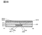
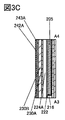
- FIG. 3A is a top view illustrating a method for manufacturing a semiconductor device according to one embodiment of the present invention.
- 3B and 3C are cross-sectional views illustrating a method for manufacturing a semiconductor device according to one embodiment of the present invention.
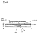
- FIG. 4A is a top view illustrating a method for manufacturing a semiconductor device according to one embodiment of the present invention.
- FIGS. 1A is a top view of a semiconductor device according to one embodiment of the present invention.
- FIGS. 1B and 1C are cross-sectional views of a semiconductor device according to one embodiment of the present invention.
- FIGS. 2A and 2B are cross-sectional views of a semiconductor
- FIG. 4B and 4C are cross-sectional views illustrating a method for manufacturing a semiconductor device according to one embodiment of the present invention.
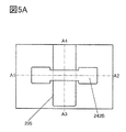
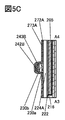
- FIG. 5A is a top view illustrating a method for manufacturing a semiconductor device according to one embodiment of the present invention.
- FIGS. 5B and 5C are cross-sectional views illustrating a method for manufacturing a semiconductor device according to one embodiment of the present invention.
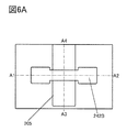
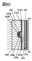
- FIG. 6A is a top view illustrating a method for manufacturing a semiconductor device according to one embodiment of the present invention.
- FIGS. 6B and 6C are cross-sectional views illustrating a method for manufacturing a semiconductor device according to one embodiment of the present invention.
- FIG. 7A is a top view illustrating a method for manufacturing a semiconductor device according to one embodiment of the present invention.
- FIGS. 7A is a top view illustrating a method for manufacturing a semiconductor device according to one embodiment of the present invention.
- FIG. 7B and 7C are cross-sectional views illustrating a method for manufacturing a semiconductor device according to one embodiment of the present invention.
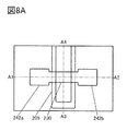
- FIG. 8A is a top view illustrating a method for manufacturing a semiconductor device according to one embodiment of the present invention.
- FIGS. 8B and 8C are cross-sectional views illustrating a method for manufacturing a semiconductor device according to one embodiment of the present invention.
- FIG. 9A is a top view illustrating a method for manufacturing a semiconductor device according to one embodiment of the present invention.
- FIGS. 9B and 9C are cross-sectional views illustrating a method for manufacturing a semiconductor device according to one embodiment of the present invention.
- FIG. 10A is a top view illustrating a method for manufacturing a semiconductor device according to one embodiment of the present invention.
- FIGS. 10A is a top view illustrating a method for manufacturing a semiconductor device according to one embodiment of the present invention.
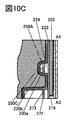
- FIG. 10B and 10C are cross-sectional views illustrating a method for manufacturing a semiconductor device according to one embodiment of the present invention.
- FIG. 11A is a top view illustrating a method for manufacturing a semiconductor device according to one embodiment of the present invention.
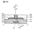
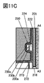
- FIGS. 11B and 11C are cross-sectional views illustrating a method for manufacturing a semiconductor device according to one embodiment of the present invention.
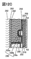
- FIG. 12A is a top view illustrating a method for manufacturing a semiconductor device according to one embodiment of the present invention.
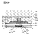
- 12B and 12C are cross-sectional views illustrating a method for manufacturing a semiconductor device according to one embodiment of the present invention.
- FIG. 13 is a top view illustrating a microwave processing apparatus according to one embodiment of the present invention.
- FIG. 14 is a cross-sectional view illustrating a microwave processing apparatus according to one embodiment of the present invention.
- FIG. 15 is a cross-sectional view illustrating a microwave processing device according to one embodiment of the present invention.
- FIG. 16 is a cross-sectional view illustrating a structure of a memory device according to one embodiment of the present invention.
- FIG. 17 is a cross-sectional view illustrating a structure of a memory device according to one embodiment of the present invention.
- FIG. 18A is a block diagram illustrating a configuration example of a storage device according to one embodiment of the present invention.
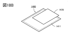
- FIG. 18B is a perspective view of a memory device according to one embodiment of the present invention.
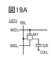
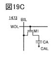
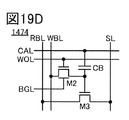
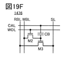
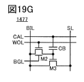
- FIGS. 19A to 19H are circuit diagrams illustrating a structure example of a memory device according to one embodiment of the present invention.
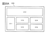
- FIG. 20A is a block diagram of a semiconductor device according to one embodiment of the present invention.
- FIG. 29B is a schematic view of a semiconductor device according to one embodiment of the present invention.
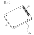
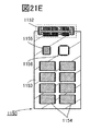
- FIGS. 21A to 21E are schematic diagrams of a memory device according to one embodiment of the present invention.
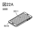
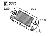
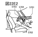
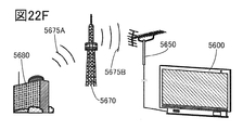
- FIGS. 22A to 22F illustrate electronic devices according to one embodiment of the present invention.
- ⁇ ⁇ Particular components may be omitted in a top view (also referred to as a “plan view”), a perspective view, and the like to facilitate understanding of the invention.
- a top view also referred to as a “plan view”
- a perspective view and the like to facilitate understanding of the invention.
- some hidden lines and the like may be omitted.
- ordinal numbers given as first, second, and the like are used for convenience, and do not indicate the order of steps or the order of lamination. Therefore, for example, the description can be made by appropriately replacing “first” with “second” or “third”.
- ordinal numbers described in this specification and the like do not always coincide with ordinal numbers used for specifying one embodiment of the present invention.
- connection relation is not limited to the predetermined connection relation, for example, the connection relation shown in the figure or the text, and it is assumed that anything other than the connection relation shown in the figure or the text is disclosed in the figure or the text.
- X and Y are objects (for example, an apparatus, an element, a circuit, a wiring, an electrode, a terminal, a conductive film, a layer, and the like).
- the functions of the source and the drain may be switched when transistors having different polarities are used or when the direction of current changes in circuit operation. For this reason, in this specification and the like, the terms of source and drain may be used interchangeably.
- a channel width in a region where a channel is actually formed may be different from a top view of the transistor.
- the indicated channel width (hereinafter, also referred to as “apparent channel width”) may be different.
- the effective channel width becomes larger than the apparent channel width, and the effect may not be negligible.
- the proportion of a channel formation region formed on the side surface of the semiconductor may be large. In that case, the effective channel width is larger than the apparent channel width.
- a simple term “channel width” may refer to an apparent channel width.
- a simple term “channel width” may refer to an effective channel width. The values of the channel length, the channel width, the effective channel width, the apparent channel width, and the like can be determined by analyzing a cross-sectional TEM image or the like.
- an impurity in a semiconductor refers to, for example, elements other than the main components of the semiconductor.
- an element having a concentration of less than 0.1 atomic% can be regarded as an impurity.
- DOS Density of State
- examples of the impurity that changes the characteristics of the semiconductor include a Group 1 element, a Group 2 element, a Group 13 element, a Group 14 element, a Group 15 element, and an oxide semiconductor.
- transition metals other than the main components such as hydrogen, lithium, sodium, silicon, boron, phosphorus, carbon, and nitrogen.
- water may function as an impurity in some cases.
- oxygen vacancies may be formed by entry of impurities, for example.
- the impurity that changes the characteristics of the semiconductor include a Group 1 element, a Group 2 element, a Group 13 element, and a Group 15 element other than oxygen and hydrogen.
- silicon oxynitride has a higher oxygen content than nitrogen as its composition.
- silicon nitride oxide has a higher nitrogen content than oxygen as its composition.
- the term “insulator” can be replaced with an insulating film or an insulating layer.
- the term “conductor” can be referred to as a conductive film or a conductive layer.
- the term “semiconductor” can be referred to as a semiconductor film or a semiconductor layer.
- parallel refers to a state in which two straight lines are arranged at an angle of -10 degrees or more and 10 degrees or less. Therefore, a case where the angle is ⁇ 5 degrees or more and 5 degrees or less is also included.
- substantially parallel refers to a state in which two straight lines are arranged at an angle of ⁇ 30 degrees or more and 30 degrees or less.
- “Vertical” means a state in which two straight lines are arranged at an angle of 80 degrees or more and 100 degrees or less. Therefore, a case where the angle is 85 degrees or more and 95 degrees or less is also included.
- substantially perpendicular refers to a state in which two straight lines are arranged at an angle of 60 degrees or more and 120 degrees or less.
- a barrier film refers to a film having a function of suppressing transmission of impurities such as water and hydrogen and oxygen, and when the barrier film has conductivity, the barrier film is referred to as a conductive barrier film. May be called.
- a metal oxide is a metal oxide in a broad sense.
- the metal oxide is classified into an oxide insulator, an oxide conductor (including a transparent oxide conductor), an oxide semiconductor (also referred to as an oxide semiconductor or simply OS), or the like.
- the metal oxide may be referred to as an oxide semiconductor in some cases.
- a transistor including an oxide or an oxide semiconductor can be referred to as a transistor including an OS @ FET or an OS transistor.
- normally-off means that when a potential is not applied to a gate or a ground potential is applied to a gate, a current per 1 ⁇ m of a channel width flowing through a transistor is 1 ⁇ 10 ⁇ 20 at room temperature. A or lower, 1 ⁇ 10 ⁇ 18 A or lower at 85 ° C., or 1 ⁇ 10 ⁇ 16 A or lower at 125 ° C.
- ⁇ Configuration example of semiconductor device> 1A, 1B, and 1C are a top view and cross-sectional views of a transistor 200 according to one embodiment of the present invention and a periphery of the transistor 200.
- FIG. 1A is a top view of a semiconductor device including the transistor 200.
- FIG. 1B and 1C are cross-sectional views of the semiconductor device.
- FIG. 1B is a cross-sectional view of a portion indicated by a dashed line A1-A2 in FIG. 1A, and is also a cross-sectional view of the transistor 200 in the channel length direction.
- 1C is a cross-sectional view of a portion indicated by a dashed-dotted line A3-A4 in FIG. 1A, and is also a cross-sectional view of the transistor 200 in the channel width direction. Note that some components are not illustrated in the top view in FIG. 1A for clarity.
- the semiconductor device of one embodiment of the present invention includes the insulator 212 over the substrate (not illustrated), the insulator 214 over the insulator 212, the transistor 200 over the insulator 214, and the insulator 280 over the transistor 200.
- the insulator 212, the insulator 214, the insulator 280, the insulator 282, the insulator 283, the insulator 274, and the insulator 281 function as an interlayer film.
- the semiconductor device includes a conductor 240 (a conductor 240a and a conductor 240b) which is electrically connected to the transistor 200 and functions as a plug.
- the insulator 241 (the insulator 241a and the insulator 241b) is provided in contact with a side surface of the conductor 240 functioning as a plug.
- a conductor 246 (a conductor 246a and a conductor 246b) which is electrically connected to the conductor 240 and functions as a wiring is provided over the insulator 281 and the conductor 240.
- an insulator 241a is provided in contact with the insulator 272, the insulator 273, the insulator 280, the insulator 282, the insulator 283, the insulator 274, and the inner wall of the opening of the insulator 281.
- a first conductor of the body 240a is provided, and a second conductor of the conductor 240a is provided further inside.
- An insulator 241b is provided in contact with the insulator 272, the insulator 273, the insulator 280, the insulator 282, the insulator 283, the insulator 274, and the inner wall of the opening of the insulator 281.
- a first conductor of the body 240b is provided, and a second conductor of the conductor 240b is further provided inside.
- the height of the upper surface of the conductor 240 and the height of the upper surface of the insulator 281 can be approximately equal.
- the transistor 200 has a structure in which the first conductor of the conductor 240 and the second conductor of the conductor 240 are stacked, the present invention is not limited to this.
- a structure in which the conductor 240 is provided as a single layer or a stacked structure of three or more layers may be employed.
- ordinal numbers may be given in the order of formation to distinguish them.
- the transistor 200 includes an insulator 216 over an insulator 214, a conductor 205 (a conductor 205 a and a conductor 205 b) which is embedded in the insulator 216, An insulator 222 on the conductor 205, an insulator 224 on the insulator 222, an oxide 230a on the insulator 224, an oxide 230b on the oxide 230a, and an oxide on the oxide 230b 243a and an oxide 243b; a conductor 242a on the oxide 243a; a conductor 242b on the oxide 243b; an oxide 230c on the oxide 230b; an insulator 250 on the oxide 230c; A conductor 260 (the conductor 260a and the conductor 260b) which is located above and overlaps with the oxide 230c; a part of the top surface of the insulator 224; An insulator 272 in contact with the side surface, the side surface of the
- the oxide 230c is in contact with the side surface of the oxide 243a, the side surface of the oxide 243b, the side surface of the conductor 242a, and the side surface of the conductor 242b.
- the conductor 260 has a conductor 260a and a conductor 260b, and the conductor 260a is arranged so as to cover the bottom and side surfaces of the conductor 260b.
- the upper surface of the conductor 260 is disposed so as to substantially coincide with the upper surface of the insulator 250 and the upper surface of the oxide 230c.
- the insulator 282 is in contact with the top surfaces of the conductor 260, the oxide 230c, the insulator 250, and the insulator 280.
- the insulator 212, the insulator 214, the insulator 222, the insulator 272, the insulator 273, the insulator 282, and the insulator 283 suppress at least one diffusion of hydrogen (eg, a hydrogen atom or a hydrogen molecule). It is preferable to have a function of Further, the insulator 212, the insulator 214, the insulator 222, the insulator 272, the insulator 273, the insulator 282, and the insulator 283 suppress diffusion of oxygen (for example, at least one of oxygen atoms and oxygen molecules).
- each of the insulator 222, the insulator 272, the insulator 273, the insulator 282, and the insulator 283 preferably has lower permeability to one or both of oxygen and hydrogen than the insulator 224.
- the insulator 212, the insulator 214, the insulator 222, the insulator 272, the insulator 273, the insulator 282, and the insulator 283 each have lower permeability to one or both of oxygen and hydrogen than the insulator 250. preferable.
- the insulator 212, the insulator 214, the insulator 222, the insulator 272, the insulator 273, the insulator 282, and the insulator 283 each have lower permeability to one or both of oxygen and hydrogen than the insulator 280. preferable.
- the insulator 272 includes an upper surface and side surfaces of the conductor 242a, an upper surface and side surfaces of the conductor 242b, a side surface of the oxide 243a, a side surface of the oxide 243b, a side surface of the oxide 230a, and a side surface of the oxide 230b. It is preferable to be in contact with the side surface and the upper surface of the insulator 224. It is preferable that the insulator 273 be provided in contact with the insulator 272. Thus, the insulator 280 is separated from the insulator 224 and the oxide 230 by the insulator 272 and the insulator 273.
- the oxide 230 includes an oxide 230a over the insulator 224, an oxide 230b over the oxide 230a, and an oxide 230c which is provided over the oxide 230b and at least part of which is in contact with the top surface of the oxide 230b. Is preferable.
- the present invention is not limited to this.
- a single layer of the oxide 230b, a two-layer structure of the oxide 230b and the oxide 230a, a two-layer structure of the oxide 230b and the oxide 230c, or a stacked structure of four or more layers may be provided.
- the oxide 230c may have a two-layer structure to provide a four-layer structure.
- the conductor 260 is illustrated as having a two-layer structure, but the present invention is not limited to this.
- the conductor 260 may have a single-layer structure or a stacked structure of three or more layers.
- the conductor 260 functions as a gate of the transistor, and the conductor 242a and the conductor 242b each function as a source electrode or a drain electrode.
- the conductor 260 functioning as a gate is formed in a self-aligned manner so as to fill an opening formed by the insulator 280 and the like. By forming the conductor 260 in this manner, the conductor 260 can be reliably disposed in a region between the conductor 242a and the conductor 242b without alignment.
- a metal oxide serving as an oxide semiconductor (hereinafter, also referred to as an oxide semiconductor) is used for the oxide 230 including the channel formation region (the oxide 230a, the oxide 230b, and the oxide 230c).
- a metal oxide which functions as an oxide semiconductor has an energy gap of 2 eV or more, preferably 2.5 eV or more.
- an In-M-Zn oxide (element M is aluminum, gallium, yttrium, tin, copper, vanadium, beryllium, boron, titanium, iron, nickel, germanium, zirconium, molybdenum, lanthanum, cerium , Neodymium, hafnium, tantalum, tungsten, or magnesium, or a plurality thereof).
- element M aluminum, gallium, yttrium, or tin is preferably used.
- an In-M oxide, an In-Zn oxide, or an M-Zn oxide may be used as the oxide 230.
- the oxide 230 includes an oxide 230a, an oxide 230b over the oxide 230a, and an oxide 230c over the oxide 230b.
- the oxide 230a is provided below the oxide 230b, diffusion of impurities from the structure formed below the oxide 230a to the oxide 230b can be suppressed.
- the oxide 230c is provided over the oxide 230b, diffusion of impurities into the oxide 230b from a structure formed above the oxide 230c can be suppressed.
- the oxide 230 preferably has a stacked structure of oxides having different atomic ratios of metal atoms. Specifically, in the metal oxide used for the oxide 230a, the atomic ratio of the element M in the constituent elements is larger than that in the metal oxide used for the oxide 230b. Is preferred. Further, in the metal oxide used for the oxide 230a, the atomic ratio of the element M to In is preferably larger than that in the metal oxide used for the oxide 230b. Further, in the metal oxide used for the oxide 230b, the atomic ratio of In to the element M is preferably larger than that in the metal oxide used for the oxide 230a. As the oxide 230c, a metal oxide that can be used for the oxide 230a or the oxide 230b can be used.
- the oxide 230b preferably has crystallinity.
- a CAAC-OS c-axis / aligned / crystalline / oxide / semiconductor
- An oxide having crystallinity, such as a CAAC-OS has a high density of impurities and defects (such as oxygen vacancies), high crystallinity, and a dense structure.
- the energy of the bottom of the conduction band of the oxide 230a and the oxide 230c be higher than the energy of the bottom of the conduction band of the oxide 230b.
- the electron affinity of the oxide 230a and the oxide 230c be smaller than the electron affinity of the oxide 230b.
- the electron affinity or the energy level Ec at the lower end of the conduction band can be determined from the ionization potential Ip, which is the difference between the vacuum level and the energy Ev at the upper end of the valence band, and the energy gap Eg.
- the ionization potential Ip can be measured, for example, by using an ultraviolet photoelectron spectroscopy (UPS) device (Ultraviolet @ Photoelectron @ Spectroscopy).
- UPS ultraviolet photoelectron spectroscopy
- the energy gap Eg can be measured using, for example, a spectroscopic ellipsometer.
- the energy level at the bottom of the conduction band gradually changes.
- the energy level at the bottom of the conduction band at the junction of the oxide 230a, the oxide 230b, and the oxide 230c changes continuously or forms a continuous junction.
- the defect state density of a mixed layer formed at the interface between the oxide 230a and the oxide 230b and the interface between the oxide 230b and the oxide 230c may be reduced.
- the main path of carriers is the oxide 230b.
- the density of defect states at the interface between the oxide 230a and the oxide 230b and the interface between the oxide 230b and the oxide 230c can be reduced. Therefore, the influence of carrier scattering due to interface scattering is small, and the transistor 200 can have high on-state current and high frequency characteristics.
- Donor in the oxide semiconductor is mainly oxygen vacancies in the oxide semiconductor (V O: oxygenvacancy also called) hydrogen is formed by being trapped in. In the following, it may be referred to as V O H that of hydrogen trapped in the oxygen deficiency.
- V OH which is a physical quantity related to the donor concentration in an oxide semiconductor.
- an oxide semiconductor may be evaluated not by a donor concentration but by a carrier concentration. Therefore, in this specification and the like, a carrier concentration which assumes a state where an electric field is not applied is used instead of a donor concentration as a parameter of an oxide semiconductor in some cases. That is, the “carrier concentration” described in this specification and the like may be referred to as the “donor concentration” in some cases.
- hydrogen in the oxide semiconductor reacts with oxygen bonded to a metal atom to become water, which may form oxygen vacancies.
- oxygen deficiency in the oxide semiconductor is increased, there is a possibility that V O H increases accordingly.
- hydrogen in an oxide semiconductor is easily moved by stress such as heat or an electric field; therefore, when a large amount of hydrogen is contained in the oxide semiconductor, reliability of the transistor might be deteriorated.
- the transistor when the concentration of hydrogen in the oxide semiconductor is increased, the transistor is likely to have normally-on characteristics, so that a semiconductor device having favorable electric characteristics and reliability cannot be formed.
- the hydrogen concentration obtained by secondary ion mass spectrometry is less than 1 ⁇ 10 20 atoms / cm 3 , preferably 1 ⁇ 10 19 atoms / cm 3. It is less than 3 , more preferably less than 5 ⁇ 10 18 atoms / cm 3 , further preferably less than 1 ⁇ 10 18 atoms / cm 3 .
- a metal oxide in which impurities such as hydrogen are sufficiently reduced is used for a channel formation region of a transistor, stable electric characteristics can be provided.
- the carrier concentration of the metal oxide semiconductor functioning as a channel formation region is preferably lower than or equal to 1 ⁇ 10 18 cm ⁇ 3 and lower than 1 ⁇ 10 17 cm ⁇ 3. Is more preferably less than 1 ⁇ 10 16 cm ⁇ 3 , further preferably less than 1 ⁇ 10 13 cm ⁇ 3 , further preferably less than 1 ⁇ 10 12 cm ⁇ 3. preferable.
- the lower limit of the carrier concentration of the metal oxide functioning as a channel formation region is not particularly limited, but can be, for example, 1 ⁇ 10 ⁇ 9 cm ⁇ 3 .
- hydrogen may diffuse into the metal oxide as the metal oxide undergoes a process after film formation.
- a deposition gas containing hydrogen may be used. The probability that hydrogen contained in the deposition gas diffuses into the oxide 230 is high.
- impurities such as hydrogen, nitrogen, and carbon exist.
- an impurity bonded to a silicon atom is difficult to remove by a heat treatment because it is necessary to break the bond between the impurity atom and the silicon atom.
- microwave treatment is preferably performed in an atmosphere containing oxygen and under reduced pressure.
- an electric field generated by the microwave is applied to the insulator 250 and the oxide 230, so that VoH in the insulator 250 and in the oxide 230 can be separated into Vo and hydrogen.
- Some of the hydrogen separated at this time may be combined with oxygen and removed as H 2 O from the insulator 250 and the oxide 230 in some cases. Further, part of hydrogen may be gettered by the conductor 242 in some cases.
- the microwave treatment the hydrogen concentrations in the insulator 250 and the oxide 230 can be reduced. Further, Vo can be repaired or supplemented by supplying oxygen to Vo that may exist after dividing VoH in the oxide 230 into Vo and hydrogen.
- the heat treatment may be performed while maintaining the reduced pressure state after the microwave treatment.
- the step of performing the heat treatment may be performed a plurality of times while maintaining the reduced pressure state after the microwave treatment. For example, after the microwave treatment is performed for 10 seconds or more and 300 seconds or less, preferably 30 seconds or more and 60 seconds or less, the heat treatment is performed for 30 seconds or more and 3000 seconds or less, preferably 300 seconds or more while maintaining the reduced pressure state. May be performed two to ten times.
- the heat treatment temperature is preferably higher than or equal to 300 ° C and lower than or equal to 500 ° C.
- the film quality of the insulator 250 is modified, so that diffusion of hydrogen, water, impurities, or the like can be suppressed. Accordingly, diffusion of hydrogen, water, or impurities to the oxide 230 through the insulator 250 is suppressed by a post-process such as formation of a conductive film to be the conductor 260 or a post-treatment such as heat treatment. be able to.
- the bond energy between hydrogen and silicon atoms is 3.3 eV
- the bond energy between carbon and silicon atoms is 3.4 eV
- the bond energy between nitrogen and silicon atoms is 3.5 eV. Therefore, in order to remove a hydrogen atom bonded to a silicon atom, a radical or an ion having an energy of at least 3.3 eV is caused to collide with a bonding portion between the hydrogen atom and the silicon atom to remove the hydrogen atom and the silicon atom.
- a bond with an atom can be broken.
- the radicals and ions generated by the plasma excited by the microwave the ground state O ( 3 P) of the oxygen atom radical, the first excited state O ( 1 D) of the oxygen atom radical, and the monovalent oxygen molecule Cation O 2 + and the like.
- the energy of O ( 3 P) is 2.42 eV
- the energy of O ( 1 D) is 4.6 eV.
- O 2 + has an electric charge and is accelerated by the potential distribution in the plasma and the bias, the energy is not uniquely determined. However, at least the internal energy alone gives energy higher than O ( 1 D). Have.
- radicals and ions such as O ( 1 D) and O 2 + cut off bonds between hydrogen, nitrogen, and carbon atoms in the insulator 250 and silicon atoms, and hydrogen bonded to silicon atoms. Nitrogen and carbon can be removed. In addition, impurities such as hydrogen, nitrogen, and carbon can be reduced by heat energy or the like applied to the substrate when performing microwave excitation plasma treatment.
- O ( 3 P) has low reactivity and does not react with the insulator 250 but diffuses deep into the film.
- O ( 3 P) reaches the oxide 230 through the insulator 250 and diffuses into the oxide 230.
- O ( 3 P) diffused into the oxide 230 approaches the oxygen vacancy containing hydrogen, the hydrogen in the oxygen vacancy is released from the oxygen vacancy, and O ( 3 P) enters the oxygen vacancy instead. Oxygen deficiency is compensated. Therefore, generation of electrons serving as carriers in the oxide 230 can be suppressed.
- the microwave treatment is preferably performed at a pressure of 133 Pa or more, preferably 200 Pa or more, and more preferably 400 Pa or more.
- the oxygen flow rate (O2 / O2 + Ar) is preferably 50% or less, more preferably 10% to 30%.
- the carrier concentration of the metal oxide which functions as a channel formation region 1.0 ⁇ 10 18 / cm 3 or less, Preferably less than 1.0 ⁇ 10 17 / cm 3 , more preferably less than 1.0 ⁇ 10 16 / cm 3 , still more preferably less than 1.0 ⁇ 10 13 / cm 3 , still more preferably 1.0 ⁇ 10 12. / Cm 3 .
- the lower limit of the carrier concentration of the metal oxide functioning as a channel formation region is not particularly limited, but can be, for example, 1 ⁇ 10 ⁇ 9 cm ⁇ 3 .
- a transistor using such a metal oxide as a channel formation region can have normally-off characteristics, so that a semiconductor device having favorable electric characteristics and reliability can be formed.
- hydrogen diffuses into the metal oxide as the metal oxide goes through a process after film formation.
- a deposition gas containing hydrogen may be used. The probability that hydrogen contained in the deposition gas diffuses into the oxide 230 is high.
- impurities such as hydrogen, nitrogen, and carbon exist.
- an impurity bonded to a silicon atom is difficult to remove by a heat treatment because it is necessary to break the bond between the impurity atom and the silicon atom.
- microwave treatment may be performed in an atmosphere containing oxygen and under reduced pressure.
- an electric field due to microwaves is applied to the insulator 280 and the oxide 230, and VoH in the insulator 280 and in the oxide 230 can be separated into Vo and hydrogen.
- Part of the hydrogen separated at this time may be combined with oxygen included in the insulator 280 and removed as H 2 O in some cases. Further, part of hydrogen may be gettered to the conductor 242 through the insulator 272 and the insulator 273 in some cases.
- the concentration of hydrogen in the insulator 280 and the hydrogen concentration in the oxide 230 can be reduced. Further, Vo can be repaired or supplemented by supplying oxygen to Vo that may exist after dividing VoH in the oxide 230 into Vo and hydrogen.
- the heat treatment may be performed while maintaining the reduced pressure state after the microwave treatment.
- hydrogen in the insulator 280 and the hydrogen in the oxide 230 can be efficiently removed.
- the step of performing the heat treatment may be performed a plurality of times while maintaining the reduced pressure state after the microwave treatment. For example, after performing the microwave treatment for 10 seconds or more and 300 seconds or less, preferably 30 seconds or more and 60 seconds or less, while maintaining the reduced pressure state, 30 seconds or more and 300 seconds or less, preferably 30 seconds or more and 300 seconds or less, preferably 300 seconds or less.
- the step of performing the heat treatment for seconds or a time close thereto may be performed twice to ten times.
- hydrogen in the insulator 280 and the hydrogen in the oxide 230 can be more efficiently removed.
- the heat treatment temperature is preferably higher than or equal to 300 ° C and lower than or equal to 500 ° C.
- the film quality of the insulator 280 is modified, so that diffusion of hydrogen, water, impurities, or the like can be suppressed. Accordingly, diffusion of hydrogen, water, or impurities into the oxide 230 through the insulator 280 can be suppressed by a post-process after the formation of the insulator 283 or heat treatment or the like. Further, it is preferable that the insulator 282 and the insulator 283 functioning as barrier insulating films be provided over the insulator 280 because hydrogen, water, or impurities can be prevented from entering the transistor 200 from the outside.
- the subsequent description is the same as the microwave treatment performed after the insulator 250 is formed, and the insulator 250 may be replaced with the insulator 280.
- an insulating film to be the insulator 280 is formed, and the insulator 280 having a flat surface is formed by performing, for example, a CMP process (Chemical Mechanical Polishing), and then the insulating film 280 is placed under an atmosphere containing oxygen and under reduced pressure. Then, microwave treatment may be performed. By performing the microwave treatment, an electric field generated by the microwave is applied to the insulator 280 and the oxide 230, and VoH in the insulator 280 and in the oxide 230 can be separated into Vo and hydrogen. Part of the hydrogen separated at this time may be combined with oxygen included in the insulator 280 and removed as H 2 O in some cases. Further, part of hydrogen may be gettered to the conductor 242 through the insulator 272 and the insulator 273 in some cases.
- CMP process Chemical Mechanical Polishing
- the insulator 280 contains oxygen by, for example, a sputtering method.
- microwave treatment may be performed in an atmosphere containing oxygen and under reduced pressure. By performing the microwave treatment, an electric field generated by the microwave is applied to the insulator 280 and the oxide 230, and VoH in the insulator 280 and in the oxide 230 can be separated into Vo and hydrogen.
- Part of the hydrogen separated at this time is combined with oxygen injected into the insulator 280 during the formation of aluminum oxide to form H 2 O, and is accumulated at the interface between the insulator 280 and aluminum oxide and near the interface. There is.
- H 2 O accumulated at the interface between the insulator 280 and the aluminum oxide and near the interface can be removed.
- part of hydrogen may be gettered to the conductor 242 through the insulator 272 and the insulator 273 in some cases.
- the microwave treatment By performing the microwave treatment in this manner, the concentration of hydrogen in the insulator 280 and the hydrogen concentration in the oxide 230 can be reduced.
- Vo can be repaired or supplemented by supplying oxygen to Vo that may exist after dividing VoH in the oxide 230 into Vo and hydrogen.
- the heat treatment may be performed while maintaining the reduced pressure state after the microwave treatment.
- hydrogen in the insulator 280 and the hydrogen in the oxide 230 can be efficiently removed.
- the step of performing the heat treatment may be performed a plurality of times while maintaining the reduced pressure state after the microwave treatment. For example, after performing the microwave treatment for 10 seconds or more and 300 seconds or less, preferably 30 seconds to 60 seconds, the heat treatment is performed for 30 seconds or more and 3000 seconds or less, preferably 300 seconds or more while maintaining the reduced pressure state.
- the steps to be performed may be performed two to ten times.
- hydrogen in the insulator 280 and the hydrogen in the oxide 230 can be more efficiently removed.
- the heat treatment temperature is preferably higher than or equal to 300 ° C and lower than or equal to 500 ° C.
- the film quality of the insulator 280 is modified, so that diffusion of hydrogen, water, impurities, or the like can be suppressed. Accordingly, diffusion of hydrogen, water, or impurities into the oxide 230 through the insulator 280 can be suppressed by a post-process after the formation of the insulator 280 or heat treatment or the like.
- the subsequent description is the same as the microwave treatment performed after the insulator 250 is formed, and the insulator 250 may be replaced with the insulator 280.
- an oxide 243 (the oxides 243a and 243b) is provided between the oxide 230b and the conductor 242 (a conductor 242a and a conductor 242b) functioning as a source or drain electrode. ) May be arranged. Since the conductor 242 is not in contact with the oxide 230, the conductor 242 can suppress absorption of oxygen of the oxide 230. That is, by preventing the conductor 242 from being oxidized, a decrease in the conductivity of the conductor 242 can be suppressed. Therefore, the oxide 243 preferably has a function of suppressing oxidation of the conductor 242.
- the oxide 243 have a function of suppressing transmission of oxygen.
- the oxide 243 having a function of suppressing oxygen permeation between the conductor 242 functioning as a source electrode and a drain electrode and the oxide 230b the electric potential between the conductor 242 and the oxide 230b can be increased. This is preferable because the resistance is reduced. With such a structure, electric characteristics of the transistor 200 and reliability of the transistor 200 can be improved.
- a metal oxide containing the element M may be used.
- the element M aluminum, gallium, yttrium, or tin is preferably used.
- the oxide 243 preferably has a higher concentration of the element M than the oxide 230b.
- Gallium oxide may be used as the oxide 243.
- a metal oxide such as an In-M-Zn oxide may be used.
- the atomic ratio of the element M to In is preferably larger than that in the metal oxide used for the oxide 230b.
- the thickness of the oxide 243 is preferably 0.5 nm or more and 5 nm or less, more preferably 1 nm or more and 3 nm or less. Further, the oxide 243 preferably has crystallinity. When the oxide 243 has crystallinity, release of oxygen in the oxide 230 can be favorably suppressed. For example, in the case where the oxide 243 has a crystal structure such as a hexagonal structure, release of oxygen in the oxide 230 may be suppressed in some cases.
- the oxide 243 is not necessarily provided. For example, even when the conductor 242 is in contact with the oxide 230b, oxidation of the conductor 242 is suppressed and the oxide 243 is not provided and the conductor 242a and the conductor 242a A body 242b may be provided.
- the conductor 242 (the conductor 242a and the conductor 242b) is in contact with the oxide 230, or the conductor 242 (the conductor 242a and the conductor 242b) is in contact with the oxide 243 (the oxide 243a and the oxide 243b). ) May cause oxygen in the oxide 230 or the oxide 243 to diffuse into the conductor 242 and oxidize the conductor 242 in some cases. Oxidation of the conductor 242 is highly likely to cause a decrease in the conductivity of the conductor 242. Note that diffusion of oxygen in the oxide 230 or oxygen in the oxide 243 to the conductor 242 is determined by the fact that the conductor 242 absorbs oxygen in the oxide 230 or the conductor 242 is in the oxide 243. In other words, it absorbs oxygen.
- the three-layer structure of the conductor 242, the different layer, and the oxide 230 (or the oxide 243) can be regarded as a three-layer structure including a metal-insulator-semiconductor, and the MIS (Metal- In some cases, the structure may be referred to as an insulator-semiconductor structure, or may be referred to as a diode junction structure having a MIS structure.
- the transistor 200 of one embodiment of the present invention has a structure in which the insulator 282 and the insulator 250 are in direct contact with each other as illustrated in FIGS. 1B and 1C.
- oxygen contained in the insulator 280 is less likely to be absorbed by the conductor 260. Accordingly, oxygen contained in the insulator 280 can be efficiently supplied to the oxide 230a and the oxide 230b through the oxide 230c; thus, oxygen vacancies in the oxide 230a and the oxide 230b can be reduced.
- electric characteristics and reliability of the transistor 200 can be improved.
- silicon nitride, silicon nitride oxide, aluminum oxide, or hafnium oxide can be used as the insulator 282.
- the insulator 272 and the insulator 273 preferably have a function of suppressing transmission of impurities such as hydrogen and water and oxygen.
- FIG. 2A is an enlarged view of a cross section of a portion indicated by a dashed line A5-A6 in FIG. 1A, and is also a cross-sectional view of a source region or a drain region of the transistor 200 in a channel width direction.
- FIG. 2A a structure in which the top surface of the conductor 242b, the side surface of the conductor 242b, the side surface of the oxide 243b, the side surface of the oxide 230a, and the side surface of the oxide 230b are covered with an insulator 272 and an insulator 273 is shown.
- the conductor 242a has a similar effect.
- the insulator 272 for example, aluminum oxide, hafnium oxide, gallium oxide, indium gallium zinc oxide, a silicon oxide film, a silicon nitride film, or a silicon nitride oxide film can be used.
- the insulator 273 for example, aluminum oxide or hafnium oxide can be used.
- FIG. 2B is an enlarged view of the right half of the transistor 200 of FIG. 1B.
- An oxide 230c is in contact with the left side surface of the conductor 240b (a portion surrounded by a dotted line in FIG. 2B), which suppresses diffusion of impurities and oxygen such as hydrogen and water from the insulator 250 to the conductor 242b. can do.
- the insulator 272 is in contact with the right side surface of the conductor 242b, so that diffusion of impurities such as hydrogen and water and oxygen from the insulator 280 to the conductor 242b can be suppressed. Note that the conductor 242a has a similar effect.
- the periphery of the conductor 242 is surrounded by the insulator 272, the oxide 230c, and the oxide 243b each having a function of suppressing transmission of impurities such as hydrogen and water and oxygen, so that Oxidation can be suppressed, so that the electrical characteristics of the transistor 200 and the reliability of the transistor 200 can be improved.
- the height of the bottom surface of the conductor 260 in a region where the oxide 230a and the oxide 230b do not overlap with the conductor 260 with respect to the bottom surface of the insulator 224 is the oxide 230b Is preferably located at a position lower than the height of the bottom surface of.
- the difference between the height of the bottom surface of the conductor 260 and the height of the bottom surface of the oxide 230b in a region where the oxide 230b and the conductor 260 do not overlap with each other is 0 nm to 100 nm, preferably 3 nm to 50 nm. Or less, more preferably 5 nm or more and 20 nm or less.
- the conductor 260 functioning as a gate covers the side surface and the upper surface of the oxide 230b in the channel formation region with the oxide 230c and the insulator 250 interposed therebetween, so that the electric field of the conductor 260 It becomes easy to act on the whole oxide 230b in the region.
- the on-state current of the transistor 200 can be increased and frequency characteristics can be improved.
- a semiconductor device having normally-off electrical characteristics can be provided.
- a semiconductor device including a transistor having high frequency characteristics can be provided.
- a semiconductor device including a transistor with low off-state current can be provided.
- the following describes a detailed structure of a semiconductor device including the transistor 200 according to one embodiment of the present invention.
- the conductor 205 is arranged so as to overlap with the oxide 230 and the conductor 260. It is preferable that the conductor 205 be provided so as to be embedded in the insulator 214 and the insulator 216.
- the conductor 260 may function as a first gate (also referred to as a top gate) electrode in some cases.
- the conductor 205 functions as a second gate (also referred to as a bottom gate) electrode.
- Vth of the transistor 200 can be controlled by changing the potential applied to the conductor 205 independently of the potential applied to the conductor 260 without changing the potential.
- Vth of the transistor 200 can be made higher than 0 V and off-state current can be reduced. Therefore, when a negative potential is applied to the conductor 205, the drain current when the potential applied to the conductor 260 is 0 V can be smaller than when no negative potential is applied.
- the conductor 205 is preferably provided to be larger than a region of the oxide 230 which does not overlap with the conductors 242a and 242b as illustrated in FIG. 1A.
- the conductor 205 preferably extends in a region outside an end portion of the oxide 230 intersecting with the channel width direction. That is, it is preferable that the conductor 205 and the conductor 260 overlap with each other with the insulator interposed outside the side surface of the oxide 230 in the channel width direction.
- charge-up local charging
- the conductor 205 may overlap with at least the oxide 230 located between the conductor 242a and the conductor 242b.
- the channel formation region can be electrically surrounded by an electric field of the conductor 260 having a function as the first gate and an electric field of the conductor 205 having a function of the second gate.
- a structure of a transistor that electrically surrounds a channel formation region by an electric field of a first gate and a second gate is referred to as a surrounded-channel (S-channel) structure.
- the S-channel structure has a feature that the side surface and the periphery of the oxide 243a in contact with the conductor 242a functioning as a source electrode and a drain electrode are I-shaped in the same manner as the channel formation region.
- the oxide semiconductor 243b has a feature in which the side surface and the periphery of the oxide 243b in contact with the conductor 242b functioning as a source electrode and a drain electrode are I-type, similarly to the channel formation region. Further, the side surface and the periphery of the oxide 243a in contact with the conductor 242a are in contact with the insulator 272, so that the oxide 243a can be I-shaped in a manner similar to that of the channel formation region. In addition, since the side surface and the periphery of the oxide 243b in contact with the conductor 242b are in contact with the insulator 272, the oxide 243b can be I-shaped as in the channel formation region.
- Form I can be treated as the same as high-purity intrinsic substance described later.
- the S-channel structure disclosed in this specification and the like is different from the Fin structure and the planar structure.
- the conductor 205a is preferably a conductor that suppresses transmission of impurities such as water or hydrogen and oxygen.
- impurities such as water or hydrogen and oxygen.
- titanium, titanium nitride, tantalum, or tantalum nitride can be used.
- the conductor 205b be formed using a conductive material mainly containing tungsten, copper, or aluminum.
- the conductor 205 is illustrated as having two layers, the conductor 205 may have a multilayer structure of three or more layers.
- the oxide semiconductor, the insulator or the conductor located in the lower layer of the oxide semiconductor, and the insulator or the conductor located in the upper layer of the oxide semiconductor are formed in different films without opening to the air. It is preferable that the seeds be continuously formed because a substantially high-purity intrinsic oxide semiconductor film in which the concentration of impurities (in particular, hydrogen and water) is reduced can be formed.
- An oxide film to be the object 230b, an oxide film to be the oxide 243, and a conductive film to be the conductor 242 may be sequentially formed.
- impurities such as water or hydrogen are mixed into the transistor 200 from the substrate side or from above. It is preferable to function as a barrier insulating film that suppresses the above.
- the insulator 212, the insulator 214, the insulator 272, the insulator 273, the insulator 282, the insulator 283, and the insulator 281 each include a hydrogen atom, a hydrogen molecule, a water molecule, a nitrogen atom, a nitrogen molecule, a nitrogen oxide molecule ( It is preferable to use an insulating material having a function of suppressing diffusion of impurities such as N 2 O, NO, and NO 2 , and copper atoms (the impurities are not easily transmitted). Alternatively, it is preferable to use an insulating material having a function of suppressing diffusion of oxygen (for example, at least one of an oxygen atom and an oxygen molecule) (the above-described oxygen is not easily transmitted).
- silicon nitride or the like be used for the insulator 212, the insulator 283, and the insulator 281, and aluminum oxide or the like be used for the insulator 214, the insulator 272, the insulator 273, and the insulator 283.
- impurities such as water or hydrogen from the substrate side to the transistor 200 side through the insulator 212 and the insulator 214
- diffusion of oxygen contained in the insulator 224 or the like to the substrate via the insulator 212 and the insulator 214 can be suppressed.
- the transistor 200 is formed using the insulator 212, the insulator 214, the insulator 272, the insulator 273, the insulator 282, and the insulator 283 each having a function of suppressing diffusion of impurities such as water or hydrogen and oxygen. It is preferable to have a surrounding structure.
- the resistivity of the insulator 212, the insulator 283, and the insulator 281 is approximately 1 ⁇ 10 13 ⁇ cm, so that the insulator 212, the insulator 283, In some cases, the insulator 281 can reduce charge-up of the conductor 205, the conductor 242, or the conductor 260.
- Insulator 212, the resistivity of the insulator 283, and the insulator 281 is preferably a 1 ⁇ 10 15 ⁇ cm or less 1 ⁇ 10 10 ⁇ cm or more.
- the insulator 216, the insulator 280, and the insulator 274 preferably have a lower dielectric constant than the insulator 214.
- a material having a low dielectric constant as an interlayer film, parasitic capacitance generated between wirings can be reduced.
- silicon oxide, silicon oxynitride, silicon nitride oxide, silicon nitride, silicon oxide to which fluorine is added, silicon oxide to which carbon is added, carbon, and nitrogen are added. Silicon oxide, silicon oxide having holes, or the like may be used as appropriate.
- the insulator 222 and the insulator 224 have a function as a gate insulator.
- the insulator 224 in contact with the oxide 230 release oxygen by heating.
- oxygen released by heating may be referred to as excess oxygen.
- the insulator 224 may be formed using silicon oxide or silicon oxynitride as appropriate.
- an oxide material from which part of oxygen is released by heating as the insulator 224.
- An oxide from which oxygen is released by heating means that the amount of released oxygen molecules is 1.0 ⁇ 10 18 molecules / cm 3 or more in thermal desorption spectroscopy (TDS (Thermal Desorption Spectroscopy) analysis).
- TDS Thermal Desorption Spectroscopy
- the surface temperature of the film at the time of the TDS analysis is preferably in the range of 100 ° C to 700 ° C, or 100 ° C to 400 ° C.
- the insulator 222 preferably functions as a barrier insulating film for preventing impurities such as water or hydrogen from entering the transistor 200 from the substrate side.
- the insulator 222 preferably has lower hydrogen permeability than the insulator 224.
- the insulator 222 have a function of suppressing diffusion of oxygen (for example, at least one of oxygen atoms and oxygen molecules) (the above-described oxygen is hardly transmitted).
- the insulator 222 preferably has lower oxygen permeability than the insulator 224. It is preferable that the insulator 222 have a function of suppressing diffusion of oxygen and impurities because diffusion of oxygen included in the oxide 230 to a lower side than the insulator 222 can be reduced.
- the conductor 205 can be prevented from reacting with oxygen included in the insulator 224 and the oxide 230.
- an insulator containing an oxide of one or both of aluminum and hafnium which are insulating materials, may be used. It is preferable to use aluminum oxide, hafnium oxide, an oxide containing aluminum and hafnium (hafnium aluminate), or the like as the insulator containing one or both oxides of aluminum and hafnium. In the case where the insulator 222 is formed using such a material, the insulator 222 suppresses release of oxygen from the oxide 230 and entry of impurities such as hydrogen from the periphery of the transistor 200 into the oxide 230. Functions as a layer.
- aluminum oxide, bismuth oxide, germanium oxide, niobium oxide, silicon oxide, titanium oxide, tungsten oxide, yttrium oxide, or zirconium oxide may be added to these insulators.
- these insulators may be nitrided. Silicon oxide, silicon oxynitride, or silicon nitride may be stacked over the above insulator.
- the insulator 222 is formed of, for example, aluminum oxide, hafnium oxide, tantalum oxide, zirconium oxide, lead zirconate titanate (PZT), strontium titanate (SrTiO 3 ), or (Ba, Sr) TiO 3 (BST).
- An insulator including a so-called high-k material may be used in a single layer or a stacked layer. When a transistor is miniaturized and highly integrated, a problem such as a leak current may occur due to thinning of a gate insulator. With the use of a high-k material for an insulator functioning as a gate insulator, reduction in gate potential at the time of transistor operation can be performed while the physical thickness is maintained.
- the insulator 222 and the insulator 224 may have a stacked structure of two or more layers.
- the structure is not limited to a laminated structure made of the same material, and may be a laminated structure made of different materials.
- An oxide 243 is provided over the oxide 230b, and a conductor 242 (a conductor 242a and a conductor 242b) functioning as a source electrode and a drain electrode is provided over the oxide 243.
- the thickness of the conductor 242 may be, for example, from 1 nm to 50 nm, preferably from 2 nm to 25 nm.
- the conductor 242 aluminum, chromium, copper, silver, gold, platinum, tantalum, nickel, titanium, molybdenum, tungsten, hafnium, vanadium, niobium, manganese, magnesium, zirconium, beryllium, indium, ruthenium, iridium, strontium, It is preferable to use a metal element selected from lanthanum, an alloy containing the above-described metal element as a component, an alloy in which the above-described metal elements are combined, or the like.
- tantalum nitride, titanium nitride, tungsten, a nitride containing titanium and aluminum, a nitride containing tantalum and aluminum, ruthenium oxide, ruthenium nitride, an oxide containing strontium and ruthenium, an oxide containing lanthanum and nickel, and the like are used. Is preferred.
- tantalum nitride, titanium nitride, nitride containing titanium and aluminum, nitride containing tantalum and aluminum, ruthenium oxide, ruthenium nitride, oxide containing strontium and ruthenium, and oxide containing lanthanum and nickel are not easily oxidized.
- a conductive material or a material that maintains conductivity even when oxygen is absorbed is preferable.
- the insulator 250 functions as a gate insulator.
- the insulator 250 is preferably provided in contact with the upper surface of the oxide 230c.
- silicon oxide, silicon oxynitride, silicon nitride oxide, silicon nitride, silicon oxide to which fluorine is added, silicon oxide to which carbon is added, silicon oxide to which carbon and nitrogen are added, or silicon oxide having holes is used. be able to.
- silicon oxide and silicon oxynitride are preferable because they are stable against heat.
- the insulator 250 is preferably formed using an insulator from which oxygen is released by heating.
- an insulator from which oxygen is released by heating is provided as the insulator 250 in contact with the upper surface of the oxide 230c, oxygen can be effectively supplied to a channel formation region of the oxide 230b.
- the concentration of impurities such as water or hydrogen in the insulator 250 is preferably reduced.
- the thickness of the insulator 250 is preferably greater than or equal to 1 nm and less than or equal to 20 nm.
- a metal oxide may be provided between the insulator 250 and the conductor 260. It is preferable that the metal oxide suppress oxygen diffusion from the insulator 250 to the conductor 260. By providing a metal oxide that suppresses diffusion of oxygen, diffusion of oxygen from the insulator 250 to the conductor 260 is suppressed. That is, a decrease in the amount of oxygen supplied to the oxide 230 can be suppressed. Further, oxidation of the conductor 260 due to oxygen of the insulator 250 can be suppressed.
- the metal oxide has a function as part of a gate insulator. Therefore, in the case where silicon oxide, silicon oxynitride, or the like is used for the insulator 250, it is preferable that the metal oxide be a high-k material having a high relative dielectric constant.
- the gate insulator has a stacked structure of the insulator 250 and the metal oxide, a stacked structure which is stable against heat and has a high relative dielectric constant can be obtained. Therefore, it is possible to reduce the gate potential applied during the operation of the transistor while maintaining the physical thickness of the gate insulator. Further, the equivalent oxide thickness (EOT) of the insulator functioning as a gate insulator can be reduced.
- EOT equivalent oxide thickness
- hafnium, aluminum, gallium, yttrium, zirconium, tungsten, titanium, tantalum, nickel, germanium, or magnesium, or a metal oxide containing two or more kinds may be used. it can.
- the metal oxide may function as part of a gate in some cases.
- a conductive material containing oxygen is preferably provided on the channel formation region side.
- a conductive material containing oxygen and a metal element contained in a metal oxide in which a channel is formed is preferably used.
- a conductive material containing the above-described metal element and nitrogen may be used.
- indium tin oxide, indium oxide containing tungsten oxide, indium zinc oxide containing tungsten oxide, indium oxide containing titanium oxide, indium tin oxide containing titanium oxide, indium zinc oxide, and silicon were added.
- Indium tin oxide may be used.
- indium gallium zinc oxide containing nitrogen may be used.
- the conductor 260 is shown in FIG. 1 as a two-layer structure, it may have a single-layer structure or a stacked structure of three or more layers.
- the conductor 260a has a function of suppressing diffusion of impurities such as a hydrogen atom, a hydrogen molecule, a water molecule, a nitrogen atom, a nitrogen molecule, a nitrogen oxide molecule (eg, N 2 O, NO, and NO 2 ), and a copper atom. It is preferable to use a material. Alternatively, it is preferable to use a conductive material having a function of suppressing diffusion of oxygen (for example, at least one of an oxygen atom and an oxygen molecule).
- the conductor 260a has a function of suppressing diffusion of oxygen, it is possible to prevent the conductor 260b from being oxidized by the oxygen contained in the insulator 250 and lowering the conductivity.
- the conductive material having a function of suppressing diffusion of oxygen for example, tantalum, tantalum nitride, ruthenium, ruthenium oxide, or the like is preferably used.
- the conductor 260b be formed using a conductive material mainly containing tungsten, copper, or aluminum. Further, since the conductor 260 also functions as a wiring, a conductor having high conductivity is preferably used. For example, a conductive material containing tungsten, copper, or aluminum as a main component can be used.
- the conductor 260b may have a stacked structure, for example, a stacked structure of titanium or titanium nitride and the above conductive material.
- the insulator 280 includes, for example, silicon oxide, silicon oxynitride, silicon nitride oxide, silicon oxide to which fluorine is added, silicon oxide to which carbon is added, silicon oxide to which carbon and nitrogen are added, or silicon oxide having holes. It is preferred to have. In particular, silicon oxide and silicon oxynitride are preferable because they are thermally stable. In particular, a material such as silicon oxide, silicon oxynitride, or silicon oxide having a hole is preferable because a region containing oxygen which is released by heating can be easily formed.
- the concentration of impurities such as water or hydrogen in the insulator 280 be reduced. Further, the upper surface of the insulator 280 may be planarized.
- the insulator 282 or the insulator 283 preferably functions as a barrier insulating film for preventing impurities such as water or hydrogen from entering the insulator 280 from above. Further, the insulator 282 or the insulator 283 preferably functions as a barrier insulating film for suppressing transmission of oxygen.
- an insulator such as aluminum oxide, silicon nitride, or silicon nitride oxide may be used, for example.
- aluminum oxide having a high blocking property against oxygen may be used, and as the insulator 283, silicon nitride having a high blocking property against hydrogen may be used.
- the insulator 274 function as an interlayer film be provided over the insulator 282. It is preferable that the insulator 274 have a reduced concentration of impurities such as water or hydrogen in the film, similarly to the insulator 224 and the like.
- the conductor 240a and the conductor 240b be formed using a conductive material mainly containing tungsten, copper, or aluminum. Further, the conductor 240a and the conductor 240b may have a stacked structure.
- the insulator 281, the insulator 274, the insulator 282, the insulator 280, the insulator 273, and the conductor which is in contact with the insulator 272 include impurities such as water or hydrogen. It is preferable to use a conductive material having a function of suppressing transmission. For example, it is preferable to use tantalum, tantalum nitride, titanium, titanium nitride, ruthenium, ruthenium oxide, or the like. Further, a conductive material having a function of suppressing transmission of impurities such as water or hydrogen may be used in a single layer or a stacked layer.
- oxygen added to the insulator 280 can be prevented from being absorbed by the conductor 240a and the conductor 240b. Further, entry of impurities such as water or hydrogen from above the insulator 281 into the oxide 230 through the conductor 240a and the conductor 240b can be suppressed.
- an insulator such as silicon nitride, aluminum oxide, or silicon nitride oxide may be used, for example. Since the insulator 241a and the insulator 241b are provided in contact with the insulator 272 and the insulator 273, impurities such as water or hydrogen from the insulator 280 or the like are mixed into the oxide 230 through the conductors 240a and 240b. Can be suppressed.
- silicon nitride is preferable because of its high blocking property against hydrogen.
- oxygen contained in the insulator 280 can be prevented from being absorbed by the conductor 240a and the conductor 240b.
- the conductor 246 (the conductor 246a and the conductor 246b) which functions as a wiring may be provided in contact with the upper surface of the conductor 240a and the upper surface of the conductor 240b.
- the conductor 246 is preferably formed using a conductive material mainly containing tungsten, copper, or aluminum. Further, the conductor may have a stacked structure, for example, a stacked structure of titanium or titanium nitride and the above conductive material. Note that the conductor may be formed so as to be embedded in an opening provided in the insulator.
- an insulator substrate As a substrate over which the transistor 200 is formed, an insulator substrate, a semiconductor substrate, or a conductor substrate may be used, for example.
- the insulator substrate include a glass substrate, a quartz substrate, a sapphire substrate, a stabilized zirconia substrate (such as a yttria-stabilized zirconia substrate), and a resin substrate.
- the semiconductor substrate include a semiconductor substrate formed using silicon and germanium, and a compound semiconductor substrate formed using silicon carbide, silicon germanium, gallium arsenide, indium phosphide, zinc oxide, and gallium oxide.
- a semiconductor substrate having an insulator region inside the above-described semiconductor substrate for example, an SOI (Silicon On Insulator) substrate.
- the conductor substrate include a graphite substrate, a metal substrate, an alloy substrate, and a conductive resin substrate.
- a substrate including a metal nitride, a substrate including a metal oxide, and the like are given.
- a substrate provided with a conductor or a semiconductor on an insulator substrate a substrate provided with a conductor or an insulator on a semiconductor substrate, a substrate provided with a semiconductor or an insulator on a conductor substrate, and the like.
- a substrate in which an element is provided may be used.
- Elements provided on the substrate include a capacitor, a resistor, a switch, a light-emitting element, a storage element, and the like.
- insulator examples include oxides, nitrides, oxynitrides, nitrided oxides, metal oxides, metal oxynitrides, and metal nitrided oxides having insulating properties.
- a high-k material is used for an insulator functioning as a gate insulator, a voltage can be reduced during operation of a transistor while a physical thickness is maintained.
- a material having a low relative dielectric constant for an insulator functioning as an interlayer film parasitic capacitance generated between wirings can be reduced. Therefore, a material may be selected according to the function of the insulator.
- Examples of the insulator having a high relative dielectric constant include gallium oxide, hafnium oxide, zirconium oxide, an oxide containing aluminum and hafnium, an oxynitride containing aluminum and hafnium, an oxide containing silicon and hafnium, and silicon and hafnium. Oxynitride or nitride containing silicon and hafnium.
- the insulator having a low relative dielectric constant includes silicon oxide, silicon oxynitride, silicon nitride oxide, silicon oxide to which fluorine is added, silicon oxide to which carbon is added, silicon oxide to which carbon and nitrogen are added, and holes. Silicon oxide, resin, or the like is given.
- a transistor including an oxide semiconductor can have stable electrical characteristics by being surrounded by an insulator having a function of suppressing transmission of impurities such as hydrogen and oxygen.
- the insulator having a function of suppressing transmission of impurities such as hydrogen and oxygen include boron, carbon, nitrogen, oxygen, fluorine, magnesium, aluminum, silicon, phosphorus, chlorine, argon, gallium, germanium, yttrium, and zirconium.
- Lanthanum, neodymium, hafnium, or an insulator containing tantalum may be used as a single layer or a stacked layer.
- an insulator having a function of suppressing transmission of impurities such as hydrogen and oxygen
- a metal oxide such as tantalum oxide, or a metal nitride such as aluminum nitride, aluminum titanium nitride, titanium nitride, silicon nitride oxide, or silicon nitride can be used.
- the insulator functioning as a gate insulator is preferably an insulator having a region containing oxygen which is released by heating.
- the oxide 230 oxygen vacancies in the oxide 230 can be compensated.
- ⁇ Conductor> Aluminum, chromium, copper, silver, gold, platinum, tantalum, nickel, titanium, molybdenum, tungsten, hafnium, vanadium, niobium, manganese, magnesium, zirconium, beryllium, indium, ruthenium, iridium, strontium, lanthanum It is preferable to use a metal element selected from the above, an alloy containing the above-described metal element as a component, an alloy in which the above-described metal elements are combined, or the like.
- tantalum nitride, titanium nitride, tungsten, a nitride containing titanium and aluminum, a nitride containing tantalum and aluminum, ruthenium oxide, ruthenium nitride, an oxide containing strontium and ruthenium, an oxide containing lanthanum and nickel, and the like are used. Is preferred.
- tantalum nitride, titanium nitride, nitride containing titanium and aluminum, nitride containing tantalum and aluminum, ruthenium oxide, ruthenium nitride, oxide containing strontium and ruthenium, and oxide containing lanthanum and nickel are not easily oxidized.
- a conductive material or a material that maintains conductivity even when oxygen is absorbed is preferable.
- a semiconductor having high electric conductivity represented by polycrystalline silicon containing an impurity element such as phosphorus, or a silicide such as nickel silicide may be used.
- a plurality of conductive layers formed using the above materials may be stacked.
- a stacked structure in which the above-described material containing a metal element and a conductive material containing oxygen are combined may be employed.
- a stacked structure in which the above-described material containing a metal element and a conductive material containing nitrogen are combined may be employed.
- a stacked structure of a combination of the above-described material containing a metal element, a conductive material containing oxygen, and a conductive material containing nitrogen may be used.
- a stacked structure in which the above-described material containing a metal element and a conductive material containing oxygen are used for a conductor functioning as a gate may be used.
- a conductive material containing oxygen is preferably provided on the channel formation region side.
- a conductive material containing oxygen and a metal element contained in a metal oxide in which a channel is formed is preferably used.
- a conductive material containing the above-described metal element and nitrogen may be used.
- a conductive material containing nitrogen such as titanium nitride or tantalum nitride may be used.
- indium tin oxide, indium oxide containing tungsten oxide, indium zinc oxide containing tungsten oxide, indium oxide containing titanium oxide, indium tin oxide containing titanium oxide, indium zinc oxide, and silicon were added.
- Indium tin oxide may be used.
- indium gallium zinc oxide containing nitrogen may be used.
- Metal oxide As the oxide 230, a metal oxide that functions as an oxide semiconductor is preferably used. Hereinafter, metal oxides applicable to the oxide 230 according to the present invention will be described.
- the metal oxide preferably contains at least indium or zinc. In particular, it preferably contains indium and zinc. In addition, it is preferable that aluminum, gallium, yttrium, tin, or the like be contained in addition thereto. In addition, one or more kinds selected from boron, titanium, iron, nickel, germanium, zirconium, molybdenum, lanthanum, cerium, neodymium, hafnium, tantalum, tungsten, magnesium, and the like may be included.
- the metal oxide is an In-M-Zn oxide containing indium, the element M, and zinc is considered.
- the element M is aluminum, gallium, yttrium, tin, or the like.
- Other elements applicable to the element M include boron, titanium, iron, nickel, germanium, zirconium, molybdenum, lanthanum, cerium, neodymium, hafnium, tantalum, tungsten, and magnesium.
- a combination of a plurality of the aforementioned elements may be used as the element M.
- a metal oxide containing nitrogen may be collectively referred to as a metal oxide. Further, a metal oxide containing nitrogen may be referred to as metal oxynitride.
- An oxide semiconductor (metal oxide) is classified into a single crystal oxide semiconductor and a non-single-crystal oxide semiconductor.
- the non-single-crystal oxide semiconductor include a CAAC-OS, a polycrystalline oxide semiconductor, an nc-OS, a pseudo-amorphous oxide semiconductor (a-like OS), and an amorphous oxide semiconductor.
- Semiconductors include a CAAC-OS, a polycrystalline oxide semiconductor, an nc-OS, a pseudo-amorphous oxide semiconductor (a-like OS), and an amorphous oxide semiconductor.
- the CAAC-OS has a c-axis orientation and a crystal structure in which a plurality of nanocrystals are connected in an ab plane direction and has a strain.
- the strain refers to a region where the orientation of the lattice arrangement changes between a region where the lattice arrangement is uniform and a region where another lattice arrangement is uniform in a region where a plurality of nanocrystals are connected.
- Nanocrystals are basically hexagonal, but are not limited to regular hexagons, and may be non-regular hexagons.
- distortion may have a lattice arrangement such as a pentagon and a heptagon.
- a lattice arrangement such as a pentagon and a heptagon.
- the CAAC-OS is a layered crystal in which a layer containing indium and oxygen (hereinafter, an In layer) and a layer containing elements M, zinc, and oxygen (hereinafter, a (M, Zn) layer) are stacked. It tends to have a structure (also called a layered structure).
- indium and the element M can be replaced with each other, and when the element M in the (M, Zn) layer is replaced with indium, it can also be referred to as an (In, M, Zn) layer.
- indium in the In layer is replaced with the element M, it can be referred to as an (In, M) layer.
- CAAC-OS is a metal oxide with high crystallinity.
- the CAAC-OS it is difficult to confirm a clear crystal grain boundary; thus, it can be said that electron mobility due to the crystal grain boundary is not easily reduced.
- CAAC-OS impurities and defects oxygen deficiency (V O: also referred to as oxygen vacancy), etc.) with little metal oxide It can be called a thing. Therefore, a metal oxide having a CAAC-OS has stable physical properties. Therefore, the metal oxide including the CAAC-OS is resistant to heat and has high reliability.
- the nc-OS has a periodic atomic arrangement in a minute region (for example, a region from 1 nm to 10 nm inclusive, particularly a region from 1 nm to 3 nm inclusive).
- a minute region for example, a region from 1 nm to 10 nm inclusive, particularly a region from 1 nm to 3 nm inclusive.
- the nc-OS may not be distinguished from an a-like @ OS or an amorphous oxide semiconductor depending on an analysis method.
- indium-gallium-zinc oxide which is a kind of metal oxide including indium, gallium, and zinc
- IGZO indium-gallium-zinc oxide
- a smaller crystal for example, the above-described nanocrystal
- a large crystal here, a crystal of several mm or a crystal of several cm.
- it may be structurally stable.
- ⁇ A-like ⁇ OS is a metal oxide having a structure between an nc-OS and an amorphous oxide semiconductor.
- a-like @ OS has voids or low density regions. That is, a-like @ OS has lower crystallinity than the nc-OS and the CAAC-OS.
- Oxide semiconductors have various structures, each having different characteristics.
- the oxide semiconductor of one embodiment of the present invention may include two or more of an amorphous oxide semiconductor, a polycrystalline oxide semiconductor, an a-like @ OS, an nc-OS, and a CAAC-OS.
- the structure of the oxide semiconductor is not particularly limited, but preferably has crystallinity.
- the oxide 230 can have a CAAC-OS structure and the oxide 243 can have a hexagonal crystal structure.
- the oxide 230 and the oxide 243 have the above crystal structure, a highly reliable semiconductor device can be obtained.
- the oxide 230a, the oxide 230c, and the oxide 243 can have substantially the same composition.
- the concentration of an alkali metal or an alkaline earth metal in a metal oxide is 1 ⁇ 10 18 atoms / cm 3 or less. , Preferably 2 ⁇ 10 16 atoms / cm 3 or less.
- ⁇ ⁇ Hydrogen contained in a metal oxide reacts with oxygen bonded to a metal atom to form water, which may form an oxygen vacancy.
- oxygen vacancy When hydrogen enters the oxygen vacancy, electrons serving as carriers are generated in some cases. Further, part of hydrogen may bond with oxygen which is bonded to a metal atom to generate an electron serving as a carrier. Therefore, a transistor including a metal oxide containing hydrogen is likely to have normally-on characteristics.
- the hydrogen concentration obtained by SIMS is less than 1 ⁇ 10 20 atoms / cm 3 , preferably less than 1 ⁇ 10 19 atoms / cm 3 , more preferably 5 ⁇ 10 18 atoms / cm 3. It is set to less than 3 , more preferably less than 1 ⁇ 10 18 atoms / cm 3 .
- a thin film with high crystallinity As a metal oxide used for a semiconductor of a transistor. With the use of the thin film, stability or reliability of the transistor can be improved.
- the thin film include a single crystal metal oxide thin film and a polycrystalline metal oxide thin film.
- forming a thin film of a single crystal metal oxide or a thin film of a polycrystalline metal oxide on a substrate requires a high-temperature or laser heating step. Therefore, the cost of the manufacturing process increases, and the throughput also decreases.
- FIG. 2B is a cross-sectional view corresponding to a portion indicated by a dashed-dotted line A1-A2 in FIG. 1A, and is also a cross-sectional view of the transistor 200 in the channel length direction.
- (C) of each drawing is a cross-sectional view corresponding to a portion indicated by a dashed line A3-A4 in (A), and is also a cross-sectional view of the transistor 200 in the channel width direction. Note that some components are not illustrated in the top view of FIG.
- a substrate (not shown) is prepared, and an insulator 212 is formed over the substrate.
- the insulator 212 is formed by a sputtering method, a chemical vapor deposition (CVD) method, a molecular beam epitaxy (MBE) method, a pulsed laser deposition (PLD: pulsed laser deposition method), or a molecular beam epitaxy (MBE) method. It can be performed using a method or the like.
- the CVD method can be classified into a plasma CVD (Plasma Enhanced CVD) method using plasma, a thermal CVD (TCVD: Thermal CVD) method using heat, an optical CVD (Photo CVD) method using light, and the like. Further, the method can be classified into a metal CVD (MCVD: Metal CVD) method and an organic metal CVD (MOCVD: Metal Organic CVD) method depending on a used raw material gas.
- a plasma CVD Pullasma Enhanced CVD
- TCVD Thermal CVD
- Photo CVD Photo CVD
- MCVD Metal CVD
- MOCVD Metal Organic CVD
- the thermal CVD method is a film formation method capable of reducing plasma damage to an object to be processed because plasma is not used.
- a wiring, an electrode, an element (eg, a transistor or a capacitor) included in a semiconductor device may be charged up by receiving charge from plasma. At this time, the accumulated charges may destroy wirings, electrodes, elements, and the like included in the semiconductor device.
- a thermal CVD method that does not use plasma, such plasma damage does not occur, so that the yield of semiconductor devices can be increased.
- a plasma film having few defects can be obtained because plasma damage does not occur during film formation.
- the ALD method utilizes the self-controlling property of atoms and can deposit atoms one by one, so that an extremely thin film can be formed, a film can be formed on a structure having a high aspect ratio, There are effects such as film formation with few defects such as holes, film formation with excellent coverage, and film formation at a low temperature.
- the ALD method includes a plasma-enhanced PEALD (Plasma Enhanced ALD) method using plasma. Utilization of plasma makes it possible to form a film at a lower temperature, which is preferable in some cases.
- Some precursors used in the ALD method contain impurities such as carbon. Therefore, a film formed by an ALD method may contain more impurities such as carbon than a film formed by another film formation method.
- the impurities can be quantified by using X-ray photoelectron spectroscopy (XPS: X-ray @ Photoelectron @ Spectroscopy).
- the CVD method and the ALD method are different from the film formation method in which particles emitted from a target or the like are deposited, and are film formation methods in which a film is formed by a reaction on the surface of a processing object. Therefore, the film formation method is less affected by the shape of the object to be processed and has good step coverage.
- the ALD method has excellent step coverage and excellent thickness uniformity, and thus is suitable for covering the surface of an opening having a high aspect ratio.
- the ALD method since the ALD method has a relatively low film formation rate, it may be preferable to use the ALD method in combination with another film formation method such as a CVD method with a high film formation rate.
- the composition of the obtained film can be controlled by the flow rate ratio of the source gas.
- a film having an arbitrary composition can be formed depending on a flow rate ratio of a source gas.
- a film whose composition is continuously changed can be formed by changing the flow ratio of the source gas while forming the film.
- silicon nitride is formed as the insulator 212 by a CVD method.
- an insulator such as silicon nitride which does not easily transmit copper as the insulator 212
- a metal such as copper which is easily diffused
- a layer (not illustrated) below the insulator 212 Diffusion of the metal into an upper layer through the insulator 212 can be suppressed.
- an insulator which does not easily transmit impurities such as water or hydrogen, such as silicon nitride diffusion of impurities such as water or hydrogen from a layer below the insulator 212 can be suppressed.
- an insulator 214 is formed over the insulator 212.
- the insulator 214 can be formed by a sputtering method, a CVD method, an MBE method, a PLD method, an ALD method, or the like.
- aluminum oxide is used for the insulator 214.
- the insulator 216 is formed over the insulator 214.
- the insulator 216 can be formed by a sputtering method, a CVD method, an MBE method, a PLD method, an ALD method, or the like.
- an opening reaching the insulator 214 is formed in the insulator 216.
- the opening includes, for example, a groove and a slit. In some cases, a region where an opening is formed is referred to as an opening.
- the opening may be formed by wet etching, but dry etching is more preferable for fine processing.
- an insulator which functions as an etching stopper film when the insulator 216 is etched to form a groove is preferably selected.
- the insulator 214 may be a silicon nitride film, an aluminum oxide film, or a hafnium oxide film.
- a conductive film to be the conductor 205a is formed.
- the conductive film preferably includes a conductor having a function of suppressing transmission of oxygen.
- tantalum nitride, tungsten nitride, titanium nitride, or the like can be used.
- a stacked film of tantalum, tungsten, titanium, molybdenum, aluminum, copper, and a molybdenum tungsten alloy can be used.
- the conductive film to be the conductor 205a can be formed by a sputtering method, a CVD method, an MBE method, a PLD method, an ALD method, or the like.
- the conductive film serving as the conductor 205a has a multilayer structure.
- tantalum nitride is formed by a sputtering method, and titanium nitride is stacked on the tantalum nitride.
- a conductive film to be the conductor 205b is formed.
- the conductive film can be formed by a plating method, a sputtering method, a CVD method, an MBE method, a PLD method, an ALD method, or the like.
- a low-resistance conductive material such as copper is formed as the conductive film to be the conductor 205b.
- part of the conductive film to be the conductor 205a and part of the conductive film to be the conductor 205b are removed, so that the insulator 216 is exposed.
- the conductor 205a and the conductor 205b remain only in the opening.
- the conductor 205 having a flat top surface can be formed.
- part of the insulator 216 may be removed by the CMP treatment (see FIG. 3).
- the conductor 205 is formed so as to be embedded in the opening of the insulator 216; however, the present embodiment is not limited to this.
- the conductor 205 is formed over the insulator 214, the insulator 216 is formed over the conductor 205, and CMP is performed on the insulator 216, so that part of the insulator 216 is removed. 205 may be exposed.
- an insulator 222 is formed over the insulator 216 and the conductor 205.
- an insulator containing an oxide of one or both of aluminum and hafnium may be formed. Note that it is preferable to use aluminum oxide, hafnium oxide, an oxide containing aluminum and hafnium (hafnium aluminate), or the like as the insulator containing one or both oxides of aluminum and hafnium.
- An insulator including an oxide of one or both of aluminum and hafnium has a barrier property to oxygen, hydrogen, and water.
- the insulator 222 has a barrier property to hydrogen and water, diffusion of hydrogen and water contained in a structure provided around the transistor 200 through the insulator 222 to the inside of the transistor 200 is suppressed. In addition, generation of oxygen vacancies in the oxide 230 can be suppressed.
- the insulator 222 can be formed by a sputtering method, a CVD method, an MBE method, a PLD method, an ALD method, or the like.
- an insulating film 224A is formed over the insulator 222.
- the insulating film 224A can be formed by a sputtering method, a CVD method, an MBE method, a PLD method, an ALD method, or the like.
- the heat treatment may be performed at a temperature of 250 ° C to 650 ° C, preferably 300 ° C to 500 ° C, more preferably 320 ° C to 450 ° C.
- the heat treatment is performed in a nitrogen or inert gas atmosphere or an atmosphere containing an oxidizing gas at 10 ppm or more, 1% or more, or 10% or more.
- the heat treatment may be performed in a reduced pressure state.
- heat treatment is performed in a nitrogen or inert gas atmosphere, and then heat treatment is performed in an atmosphere including an oxidizing gas at 10 ppm or more, 1% or more, or 10% or more to supplement desorbed oxygen. Good.
- the treatment is continuously performed at 400 ° C. for one hour in an oxygen atmosphere.
- impurities such as water and hydrogen contained in the insulating film 224A can be removed.
- the heat treatment may be performed after the insulator 222 is formed.
- the above-described heat treatment conditions can be used.
- plasma treatment including oxygen may be performed under reduced pressure.
- an apparatus having a power supply for generating high-density plasma using microwaves for example.
- a power supply for applying a high frequency such as RF may be provided on the substrate side.
- high-density plasma high-density oxygen radicals can be generated.
- oxygen radicals generated by high-density plasma can be efficiently guided into the insulating film 224A. it can.
- plasma treatment including oxygen may be performed to supplement desorbed oxygen. Note that by appropriately selecting the conditions of the plasma treatment, impurities such as water and hydrogen contained in the insulating film 224A can be removed. In that case, the heat treatment may not be performed.
- aluminum oxide may be formed over the insulating film 224A by, for example, a sputtering method, and CMP may be performed until the aluminum oxide reaches the insulating film 224A.
- CMP planarization of the surface of the insulating film 224A and planarization of the surface of the insulating film 224A can be performed.
- the insulating film 224A may be partially polished by CMP to reduce the thickness of the insulating film 224A; however, the thickness may be adjusted when the insulating film 224A is formed.
- planarizing and smoothing the surface of the insulating film 224A By planarizing and smoothing the surface of the insulating film 224A, deterioration of the coverage of an oxide film to be formed later can be prevented, and reduction in the yield of a semiconductor device can be prevented in some cases. It is preferable that aluminum oxide be formed over the insulating film 224A by a sputtering method because oxygen can be added to the insulating film 224A.
- an oxide film 230A and an oxide film 230B are sequentially formed on the insulating film 224A (see FIG. 3).
- the oxide film is preferably formed continuously without exposure to the air environment.
- impurities or moisture from the atmospheric environment can be prevented from being attached to the oxide films 230A and 230B, and the vicinity of the interface between the oxide films 230A and 230B can be reduced. Can be kept clean.
- the oxide films 230A and 230B can be formed by a sputtering method, a CVD method, an MBE method, a PLD method, an ALD method, or the like.
- the oxide films 230A and 230B are formed by a sputtering method
- oxygen or a mixed gas of oxygen and a rare gas is used as a sputtering gas.
- excess oxygen in the oxide film to be formed can be increased.
- the above In-M-Zn oxide target can be used.
- the proportion of oxygen contained in the sputtering gas of the oxide film 230A may be 70% or more, preferably 80% or more, and more preferably 100%.
- the proportion of oxygen contained in a sputtering gas is greater than or equal to 1% and less than or equal to 30%, preferably greater than or equal to 5% and less than or equal to 20%. It is formed.
- a transistor using an oxygen-deficient oxide semiconductor for a channel formation region can have relatively high field-effect mobility.
- the crystallinity of the oxide film can be improved. Note that one embodiment of the present invention is not limited to this.
- the proportion of oxygen contained in the sputtering gas is more than 30% and less than or equal to 100%, preferably greater than or equal to 70% and less than or equal to 100%. Is formed.
- a transistor using an oxygen-excess oxide semiconductor for a channel formation region has relatively high reliability.
- each oxide film may be formed in accordance with characteristics required for the oxide 230 by appropriately selecting a deposition condition and an atomic ratio.
- heat treatment may be performed.
- the above-described heat treatment conditions can be used.
- impurities such as water and hydrogen in the oxide films 230A and 230B can be removed.
- the treatment is continuously performed at 400 ° C. for one hour in an oxygen atmosphere.
- an oxide film 243A is formed on the oxide film 230B (see FIG. 3).
- the oxide film 243A can be formed by a sputtering method, a CVD method, an MBE method, a PLD method, an ALD method, or the like.
- the atomic ratio of Ga to In is preferably larger than the atomic ratio of Ga to In in the oxide film 230B.
- the conductive film 242A is formed on the oxide film 243A (see FIG. 3).
- the conductive film 242A can be formed by a sputtering method, a CVD method, an MBE method, a PLD method, an ALD method, or the like.
- the oxide film 230A, the oxide film 230B, the oxide layer 243B, and the conductor layer are formed by processing the oxide film 230A, the oxide film 230B, the oxide film 243A, and the conductive film 242A into an island shape using a lithography method. 242B is formed (see FIG. 4).
- the processing can use a dry etching method or a wet etching method. Processing by dry etching is suitable for fine processing.
- the thickness of a region of the insulating film 224A which does not overlap with the oxide 230a may be reduced.
- a resist mask is formed by removing or leaving the exposed region using a developing solution.
- a conductor, a semiconductor, an insulator, or the like can be processed into a desired shape.
- a resist mask may be formed by exposing the resist using KrF excimer laser light, ArF excimer laser light, EUV (Extreme Ultraviolet) light, or the like.
- a liquid immersion technique may be used in which a liquid (for example, water) is filled between the substrate and the projection lens to perform exposure.
- an electron beam or an ion beam may be used instead of the above-described light.
- the resist mask can be removed by dry etching such as ashing, wet etching, wet etching after dry etching, or dry etching after wet etching.
- a hard mask made of an insulator or a conductor may be used instead of the resist mask.
- an insulating film or a conductive film serving as a hard mask material is formed over the conductive film 242A, a resist mask is formed thereover, and the hard mask material is etched to form a hard mask having a desired shape. can do.
- the etching of the conductive film 242A and the like may be performed after removing the resist mask, or may be performed with the resist mask left. In the latter case, the resist mask may disappear during the etching.
- the hard mask may be removed by etching.
- the material of the hard mask does not affect the post-process or can be used in the post-process, it is not always necessary to remove the hard mask.
- a capacitively coupled plasma (CCP) etching apparatus having parallel plate electrodes can be used.
- the capacitively coupled plasma etching apparatus having the parallel plate type electrode may be configured to apply a high frequency power to one of the parallel plate type electrodes.
- a configuration in which a plurality of different high-frequency power sources are applied to one of the parallel plate electrodes may be employed.
- a configuration in which a high-frequency power source having the same frequency is applied to each of the parallel plate electrodes may be employed.
- a configuration may be employed in which high-frequency power sources having different frequencies are applied to the respective parallel plate electrodes.
- a dry etching apparatus having a high-density plasma source can be used.
- an inductively coupled plasma (ICP) etching apparatus or the like can be used.
- the oxide 230a, the oxide 230b, the oxide layer 243B, and the conductor layer 242B are formed so as to at least partially overlap the conductor 205.
- the side surfaces of the oxide 230a, the oxide 230b, the oxide layer 243B, and the conductor layer 242B are preferably substantially perpendicular to the top surface of the insulator 222.
- the area can be reduced when the plurality of transistors 200 is provided. Higher densities are possible.
- the angle formed between the oxide 230a, the oxide 230b, the oxide layer 243B, and the top surface of the conductor layer 242B and the insulator 222 may be low.
- the angle formed between the side surface of the oxide 230a, the oxide 230b, the oxide layer 243B, and the conductor layer 242B and the upper surface of the insulator 222 is preferably greater than or equal to 60 ° and less than 70 °.
- a curved surface is provided between the side surface of the conductor layer 242B and the upper surface of the conductor layer 242B. That is, the end of the side surface and the end of the upper surface are preferably curved (hereinafter also referred to as a round shape).
- the curved surface has, for example, a radius of curvature of 3 nm or more and 10 nm or less, preferably 5 nm or more and 6 nm or less at an end of the conductor layer 242B. By not having a corner at the end, coverage of the film in the subsequent film forming process is improved.
- an insulating film 272A is formed over the insulating film 224A, the oxide 230a, the oxide 230b, the oxide layer 243B, and the conductor layer 242B (see FIG. 5).
- the insulating film 272A can be formed by a sputtering method, a CVD method, an MBE method, a PLD method, an ALD method, or the like.
- an insulating film having a function of suppressing transmission of oxygen is preferably used.
- aluminum oxide, silicon nitride, silicon oxide, or gallium oxide may be formed by a sputtering method or an ALD method.
- an insulating film 273A is formed over the insulating film 272A (see FIG. 5).
- the insulating film 273A can be formed by a sputtering method, a CVD method, an MBE method, a PLD method, an ALD method, or the like.
- an aluminum oxide film is formed by an ALD method. Note that a structure in which the insulating film 273A is not formed may be employed.
- an insulating film to be the insulator 280 is formed over the insulating film 273A.
- the insulating film to be the insulator 280 can be formed by a sputtering method, a CVD method, an MBE method, a PLD method, an ALD method, or the like.
- a silicon oxide film may be formed using a sputtering method and a silicon oxide film may be formed thereover using a PEALD method or a thermal ALD method.
- CMP treatment is performed on the insulating film to be the insulator 280 to form the insulator 280 having a flat top surface (see FIG. 6).
- microwave processing may be performed.
- the microwave treatment is preferably performed in an atmosphere containing oxygen and under reduced pressure.
- an electric field generated by the microwave 290 is applied to the insulator 280, the oxide 230a, and the oxide 230b, and VoH of the insulator 280, the oxide 230a, and the oxide 230b is separated into Vo and hydrogen.
- Part of the hydrogen separated at this time may be combined with oxygen included in the insulator 280 and removed as H 2 O in some cases. Further, part of hydrogen may be gettered to the conductor 242 through the insulator 272 and the insulator 273 in some cases.
- the heat treatment may be performed while maintaining the reduced pressure state after the microwave treatment.
- hydrogen in the insulator 280, the oxide 230a, and the oxide 230b can be efficiently removed.
- the step of performing the heat treatment may be performed a plurality of times while maintaining the reduced pressure state after the microwave treatment.
- a step of performing a microwave treatment for 10 seconds to 300 seconds, preferably 30 seconds to 60 seconds, and then performing a heat treatment for 30 seconds to 3000 seconds, preferably 300 seconds or near the same while maintaining the reduced pressure state May be performed two to ten times.
- the heat treatment temperature is preferably higher than or equal to 300 ° C and lower than or equal to 500 ° C.
- the film quality of the insulator 280 is modified, so that diffusion of hydrogen, water, impurities, or the like can be suppressed. Therefore, diffusion of hydrogen, water, or impurities into the oxide 230 through the insulator 280 can be suppressed by a post-process after the formation of the insulator 280 or heat treatment (see FIG. 6).
- the configuration of the microwave processing device will be described later.
- An insulating film to be the insulator 280 is formed, and the insulator 280 having a flat surface is formed by performing, for example, a CMP process, and the insulator 280 is formed over the insulator 280 in an atmosphere containing oxygen by, for example, a sputtering method.
- microwave treatment may be performed in an atmosphere containing oxygen and under reduced pressure. By performing the microwave treatment, an electric field generated by the microwave 290 is applied to the insulator 280 and the oxide 230, and VoH in the insulator 280 and in the oxide 230 can be separated into Vo and hydrogen.
- Part of the hydrogen separated at this time is combined with oxygen injected into the insulator 280 during the formation of aluminum oxide to form H 2 O, and is accumulated at the interface between the insulator 280 and aluminum oxide and near the interface. There is.
- H 2 O accumulated at the interface between the insulator 280 and aluminum oxide and near the interface can be removed.
- part of hydrogen may be gettered to the conductor 242 through the insulator 272 and the insulator 273 in some cases.
- the microwave treatment in this manner, the concentration of hydrogen in the insulator 280 and the hydrogen concentration in the oxide 230 can be reduced.
- Vo can be repaired or supplemented by supplying oxygen to Vo that may exist after dividing VoH in the oxide 230 into Vo and hydrogen.
- the heat treatment may be performed while maintaining the reduced pressure state after the microwave treatment.
- hydrogen in the insulator 280 and the hydrogen in the oxide 230 can be efficiently removed.
- the step of performing the heat treatment may be performed a plurality of times while maintaining the reduced pressure state after the microwave treatment. For example, after performing the microwave treatment for 10 seconds or more and 300 seconds or less, preferably 30 seconds to 60 seconds, the heat treatment is performed for 30 seconds or more and 3000 seconds or less, preferably 300 seconds or more while maintaining the reduced pressure state.
- the steps to be performed may be performed two to ten times.
- hydrogen in the insulator 280 and the hydrogen in the oxide 230 can be more efficiently removed.
- the heat treatment temperature is preferably higher than or equal to 300 ° C and lower than or equal to 500 ° C.
- the film quality of the insulator 280 is modified, so that diffusion of hydrogen, water, impurities, or the like can be suppressed. Accordingly, diffusion of hydrogen, water, or impurities into the oxide 230 through the insulator 280 can be suppressed by a post-process after the formation of the insulator 280 or heat treatment or the like.
- the above is a different microwave processing method.
- part of the insulator 280, part of the insulating film 273A, part of the insulating film 272A, part of the oxide layer 243B, and part of the conductor layer 242B are processed to reach the oxide 230b.
- Form an opening The opening is preferably formed so as to overlap with the conductor 205.
- the oxide 243a, the oxide 243b, the conductor 242a, the conductor 242b, the insulator 272, the insulator 273, and the insulator 224 are formed (see FIG. 7).
- part of the insulator 280 is processed by dry etching
- part of the insulating film 273A is processed by wet etching
- part of the insulating film 272A, part of the oxide layer 243B, and the conductor layer 242B May be processed by a dry etching method.
- impurities due to an etching gas or the like may be attached or diffused to the surface or the inside of the oxide 230a and the oxide 230b.
- impurities include fluorine and chlorine.
- ⁇ Cleaning is performed to remove the above impurities.
- the cleaning method include wet cleaning using a cleaning liquid, plasma treatment using plasma, cleaning by heat treatment, and the like, and the above cleaning may be appropriately combined.
- Wet cleaning may be performed using an aqueous solution obtained by diluting oxalic acid, phosphoric acid, ammonia water, hydrofluoric acid, or the like with carbonated water or pure water. Alternatively, ultrasonic cleaning using pure water or carbonated water may be performed.
- Heat treatment may be performed after the etching or after the cleaning.
- the heat treatment may be performed, for example, at 100 ° C or higher and 400 ° C or lower.
- the heat treatment is performed in an atmosphere of a nitrogen gas or an inert gas, or an atmosphere containing an oxidizing gas at 10 ppm or more, 1% or more, or 10% or more.
- the heat treatment may be performed in an oxygen atmosphere. Thereby, oxygen is supplied to the oxide 230a and oxides 230b, it is possible to reduce the oxygen vacancies V O.
- the heat treatment may be performed in a reduced pressure state.
- the heat treatment may be performed in an atmosphere containing an oxidizing gas at 10 ppm or more, 1% or more, or 10% or more in order to compensate desorbed oxygen after heat treatment in an atmosphere of nitrogen gas or an inert gas. Good.
- heat treatment may be performed.
- the heat treatment may be performed under reduced pressure, and the oxide film 230C may be formed continuously without exposure to the air (see FIG. 8). Further, the heat treatment is preferably performed in an atmosphere containing oxygen. By performing such a treatment, moisture and hydrogen adsorbed on the surface of the oxide 230b and the like can be removed, and the moisture concentration and the hydrogen concentration in the oxide 230a and the oxide 230b can be further reduced.
- the temperature of the heat treatment is preferably from 100 ° C to 400 ° C, more preferably from 150 ° C to 350 ° C. In this embodiment, the temperature of the heat treatment is set to 200 ° C. and the heat treatment is performed under reduced pressure.
- the side surface of the oxide 230a at least part of the side surface of the oxide 230a, part of the side surface and part of the top surface of the oxide 230b, part of the side surface of the oxide 243, part of the side surface of the conductor 242, It is preferable to be provided so as to be in contact with the side surface of the insulator 272, the side surface of the insulator 273, and the side surface of the insulator 280. Since the conductor 242 is surrounded by the oxide 243, the insulator 272, and the oxide film 230C, a decrease in conductivity due to oxidation of the conductor 242 in subsequent steps can be suppressed.
- the oxide film 230C can be formed by a sputtering method, a CVD method, an MBE method, a PLD method, an ALD method, or the like.
- the oxide film 230C the atomic ratio of Ga to In is preferably larger than the atomic ratio of Ga to In in the oxide film 230B.
- the oxide film 230C may be a stacked layer.
- part of oxygen contained in the sputtering gas may be supplied to the oxides 230a and 230b.
- part of oxygen contained in a sputtering gas may be supplied to the insulator 280 when the oxide film 230C is formed. Therefore, the proportion of oxygen contained in the sputtering gas of the oxide film 230C may be 70% or more, preferably 80% or more, and more preferably 100%.
- heat treatment may be performed.
- the heat treatment may be performed under reduced pressure, and the insulating film 250A may be formed continuously without exposure to the air.
- moisture and hydrogen adsorbed on the surface of the oxide film 230C and the like can be removed, and the moisture concentration and the hydrogen concentration in the oxide 230a, the oxide 230b, and the oxide film 230C can be further reduced. it can.
- the temperature of the heat treatment is preferably from 100 ° C to 400 ° C. In this embodiment, the temperature of the heat treatment is set to 200 ° C.
- microwave treatment may be performed in an atmosphere containing oxygen and under reduced pressure.
- an electric field generated by the microwave 291 is applied to the insulating film 250A, the oxide 230a, and the oxide 230b, and VoH in the insulating film 250A, the oxide 230a, and the oxide 230b is changed to Vo. It can be separated from hydrogen. Part of the hydrogen separated at this time may be combined with oxygen and removed as H 2 O from the insulating film 250A, the oxide 230a, and the oxide 230b in some cases. Further, part of hydrogen may be gettered by the conductor 242 in some cases.
- the concentration of hydrogen in the insulating film 250A, the oxide 230a, and the oxide 230b can be reduced.
- Vo can be repaired or supplemented by supplying oxygen to Vo which may exist after the VoH in the oxide 230a and the oxide 230b is divided into Vo and hydrogen.
- the heat treatment may be performed while maintaining the reduced pressure state after the microwave treatment.
- the step of performing the heat treatment may be performed a plurality of times while maintaining the reduced pressure state after the microwave treatment. For example, after the microwave treatment is performed for 10 seconds or more and 300 seconds or less, preferably 30 seconds or more and 60 seconds or less, the heat treatment is performed for 30 seconds or more and 3000 seconds or less, preferably 300 seconds or more while maintaining the reduced pressure state. May be performed two to ten times.
- the heat treatment temperature is preferably higher than or equal to 300 ° C and lower than or equal to 500 ° C.
- the quality of the insulating film 250A is modified, so that diffusion of hydrogen, water, impurities, or the like can be suppressed. Accordingly, diffusion of hydrogen, water, or impurities to the oxide 230 through the insulator 250 is suppressed by a post-process such as formation of a conductive film to be the conductor 260 or a post-treatment such as heat treatment. (See FIG. 9). The configuration of the microwave processing device will be described later.
- a conductive film 260Aa and a conductive film 260Ab are formed.
- the conductive films 260Aa and 260Ab can be formed by a sputtering method, a CVD method, an MBE method, a PLD method, an ALD method, or the like.
- a CVD method it is preferable to use a CVD method.
- the conductive film 260Aa is formed by an ALD method
- the conductive film 260Ab is formed by a CVD method (see FIG. 10).
- heat treatment may be performed.
- treatment is performed at 400 ° C. for one hour in a nitrogen atmosphere.
- the moisture concentration and the hydrogen concentration in the insulator 250 and the insulator 280 can be reduced.
- the insulator 282 is formed over the conductor 260, the oxide 230c, the insulator 250, and the insulator 280.
- the insulator 282 can be formed by a sputtering method, a CVD method, an MBE method, a PLD method, an ALD method, or the like (see FIG. 12).
- oxygen can be added to the insulator 280 while the film is formed. At this time, it is preferable to form the insulator 280 while heating the substrate.
- oxygen in the insulator 280 can be prevented from being absorbed by the conductor 260 in a heat treatment performed later, which is preferable. .
- an insulator 283 is formed over the insulator 282.
- the insulator 283 can be formed by a sputtering method, a CVD method, an MBE method, a PLD method, an ALD method, or the like (see FIG. 12).
- a film of silicon nitride or silicon nitride oxide is preferably used.
- heat treatment may be performed.
- treatment is performed at 400 ° C. for one hour in a nitrogen atmosphere.
- oxygen added by the formation of the insulator 282 can be diffused into the insulator 280 and further supplied to the oxide 230a and the oxide 230b through the oxide 230c.
- the heat treatment is not limited to after the formation of the insulator 283 and may be performed after the formation of the insulator 282.
- microwave treatment may be performed in an atmosphere containing oxygen and under reduced pressure.
- an electric field generated by the microwave 292 is applied to the insulator 280 and the oxide 230, and VoH in the insulator 280 and in the oxide 230 can be separated into Vo and hydrogen.
- Part of the hydrogen separated at this time may be combined with oxygen included in the insulator 280 and removed as H 2 O in some cases.
- part of hydrogen may be gettered to the conductor 242 through the insulator 272 and the insulator 273 in some cases.
- the concentration of hydrogen in the insulator 280 and the hydrogen concentration in the oxide 230 can be reduced.
- Vo can be repaired or supplemented by supplying oxygen to Vo that may exist after dividing VoH in the oxide 230 into Vo and hydrogen.
- the heat treatment may be performed while maintaining the reduced pressure state after the microwave treatment.
- hydrogen in the insulator 280 and the hydrogen in the oxide 230 can be efficiently removed.
- the step of performing the heat treatment may be performed a plurality of times while maintaining the reduced pressure state after the microwave treatment. For example, after performing the microwave treatment for 10 seconds or more and 300 seconds or less, preferably 30 seconds or more and 60 seconds or less, while maintaining the reduced pressure state, 30 seconds or more and 300 seconds or less, preferably 30 seconds or more and 300 seconds or less, preferably 300 seconds or less.
- the step of performing the heat treatment for seconds or a time close thereto may be performed twice to ten times.
- hydrogen in the insulator 280 and the hydrogen in the oxide 230 can be more efficiently removed.
- the heat treatment temperature is preferably higher than or equal to 300 ° C and lower than or equal to 500 ° C.
- the film quality of the insulator 280 is modified, so that diffusion of hydrogen, water, impurities, or the like can be suppressed. Accordingly, diffusion of hydrogen, water, or impurities into the oxide 230 through the insulator 280 can be suppressed by a post-process after the formation of the insulator 283 or heat treatment or the like. Further, by disposing the insulator 282 and the insulator 283 functioning as a barrier insulating film over the insulator 280, entry of hydrogen, water, or impurities from the outside into the transistor 200 can be suppressed; See FIG. 12). The configuration of the microwave processing device will be described later.
- the insulator 274 may be formed over the insulator 283.
- the insulator 274 can be formed by a sputtering method, a CVD method, an MBE method, a PLD method, an ALD method, or the like.
- the insulator 281 may be formed over the insulator 274.
- the insulator 281 can be formed by a sputtering method, a CVD method, an MBE method, a PLD method, an ALD method, or the like.
- a silicon nitride film is preferably formed by a sputtering method.
- openings are formed in the insulator 272, the insulator 273, the insulator 280, the insulator 282, the insulator 283, the insulator 274, and the insulator 281 to reach the conductor 242a and the conductor 242b.
- the formation of the opening may be performed using a lithography method.
- an insulating film to be the insulator 241 is formed, and the insulating film is anisotropically etched to form the insulator 241.
- the conductive film can be formed by a sputtering method, a CVD method, an MBE method, a PLD method, an ALD method, or the like.
- an insulating film having a function of suppressing transmission of oxygen is preferably used.
- silicon nitride is preferably formed by a PEALD method. Silicon nitride is preferable because of its high blocking property against hydrogen.
- a dry etching method or the like may be used as the anisotropic etching of the insulating film to be the insulator 241.
- a dry etching method or the like may be used.
- permeation of oxygen from the outside can be suppressed, and oxidation of the conductor 240a and the conductor 240b to be formed next can be prevented.
- diffusion of impurities such as water and hydrogen from the conductor 240a and the conductor 240b to the outside can be prevented.
- a conductive film to be the conductor 240a and the conductor 240b is formed. It is preferable that the conductive film to be the conductor 240a and the conductor 240b have a stacked structure including a conductor having a function of suppressing transmission of impurities such as water and hydrogen. For example, a stack of tantalum nitride, titanium nitride, or the like and tungsten, molybdenum, copper, or the like can be used.
- the conductive film to be the conductor 240 can be formed by a sputtering method, a CVD method, an MBE method, a PLD method, an ALD method, or the like.
- part of the conductive film to be the conductor 240a and the conductor 240b is removed, so that the insulator 281 is exposed.
- the conductive film remains only in the opening, so that the conductor 240a and the conductor 240b having a flat top surface can be formed (see FIG. 1).
- part of the insulator 281 may be removed by the CMP treatment.
- the conductive film to be the conductor 246 can be formed by a sputtering method, a CVD method, an MBE method, a PLD method, an ALD method, or the like.
- the conductive film serving as the conductor 246 is processed by lithography to form the conductor 246a in contact with the upper surface of the conductor 240a and the conductor 246b in contact with the upper surface of the conductor 240b (see FIG. 1).
- a semiconductor device including the transistor 200 illustrated in FIG. 1 can be manufactured. As illustrated in FIGS. 3 to 12, the transistor 200 can be manufactured by using the method for manufacturing a semiconductor device described in this embodiment.
- a semiconductor device having favorable electric characteristics can be provided.
- a semiconductor device having normally-off electric characteristics can be provided.
- a highly reliable semiconductor device can be provided.
- a semiconductor device with high on-state current can be provided.
- a semiconductor device having high frequency characteristics can be provided.
- a semiconductor device which can be miniaturized or highly integrated can be provided.
- a semiconductor device with low off-state current can be provided.
- a semiconductor device with reduced power consumption can be provided.
- a semiconductor device with high productivity can be provided.
- FIG. 13 schematically shows a top view of a single-wafer multi-chamber manufacturing apparatus 2700.
- the manufacturing apparatus 2700 includes an atmosphere-side substrate supply chamber 2701 having a cassette port 2761 for accommodating a substrate, an alignment port 2762 for aligning the substrate, and an atmosphere-side substrate transport for transporting the substrate from the atmosphere-side substrate supply chamber 2701.
- An unload lock chamber 2703b for switching from atmospheric pressure to reduced pressure, a transfer chamber 2704 for transferring a substrate in vacuum, a chamber 2706a, a chamber 2706b, a chamber 2706c, and a chamber 2706d are provided.
- the atmosphere-side substrate transfer chamber 2702 is connected to the load lock chamber 2703a and the unload lock chamber 2703b, the load lock chamber 2703a and the unload lock chamber 2703b are connected to the transfer chamber 2704, and the transfer chamber 2704 is connected to the chamber 2706a. , Chamber 2706b, chamber 2706c and chamber 2706d.
- a gate valve GV is provided at a connection portion of each chamber, and each chamber can be independently maintained in a vacuum state except for the atmosphere-side substrate supply chamber 2701 and the atmosphere-side substrate transfer chamber 2702.
- a transfer robot 2763a is provided in the atmosphere-side substrate transfer chamber 2702, and a transfer robot 2763b is provided in the transfer chamber 2704.
- a substrate can be transferred in the manufacturing apparatus 2700 by the transfer robot 2763a and the transfer robot 2763b.
- the back pressure (total pressure) of the transfer chamber 2704 and each chamber is, for example, 1 ⁇ 10 ⁇ 4 Pa or less, preferably 3 ⁇ 10 ⁇ 5 Pa or less, and more preferably 1 ⁇ 10 ⁇ 5 Pa or less.
- the partial pressure of gas molecules (atoms) having a mass-to-charge ratio (m / z) of 18 in the transfer chamber 2704 and each chamber is, for example, 3 ⁇ 10 ⁇ 5 Pa or less, and preferably 1 ⁇ 10 ⁇ 5 Pa or less. And more preferably 3 ⁇ 10 ⁇ 6 Pa or less.
- the partial pressure of gas molecules (atoms) whose m / z is 28 in the transfer chamber 2704 and each chamber is, for example, 3 ⁇ 10 ⁇ 5 Pa or less, preferably 1 ⁇ 10 ⁇ 5 Pa or less, and more preferably 3 ⁇ 10 ⁇ 5 Pa or less. ⁇ 10 ⁇ 6 Pa or less. Further, the partial pressure of gas molecules (atoms) whose m / z is 44 in the transfer chamber 2704 and each chamber is, for example, 3 ⁇ 10 ⁇ 5 Pa or less, preferably 1 ⁇ 10 ⁇ 5 Pa or less, and more preferably 3 ⁇ 10 ⁇ 5 Pa or less. ⁇ 10 ⁇ 6 Pa or less.
- the total pressure and partial pressure in the transfer chamber 2704 and each chamber can be measured using a mass spectrometer.
- a mass spectrometer manufactured by ULVAC, Inc. (also referred to as Q-mass) Jo @ CGM-051 may be used.
- the transfer chamber 2704 and each chamber have a configuration in which external leakage or internal leakage is small.
- the leak rate of the transfer chamber 2704 and each chamber is set to 3 ⁇ 10 ⁇ 6 Pa ⁇ m 3 / s or less, preferably 1 ⁇ 10 ⁇ 6 Pa ⁇ m 3 / s or less.
- the leak rate of gas molecules (atoms) having m / z of 18 is set to 1 ⁇ 10 ⁇ 7 Pa ⁇ m 3 / s or less, preferably 3 ⁇ 10 ⁇ 8 Pa ⁇ m 3 / s or less.
- the leak rate of gas molecules (atoms) having m / z of 28 is set to 1 ⁇ 10 ⁇ 5 Pa ⁇ m 3 / s or less, preferably 1 ⁇ 10 ⁇ 6 Pa ⁇ m 3 / s or less.
- the leak rate of gas molecules (atoms) whose m / z is 44 is set to 3 ⁇ 10 ⁇ 6 Pa ⁇ m 3 / s or less, preferably 1 ⁇ 10 ⁇ 6 Pa ⁇ m 3 / s or less.
- leak rate may be derived from the total pressure and the partial pressure measured using the mass spectrometer described above.
- Leak rate depends on external and internal leaks.
- An external leak is a gas flowing from outside the vacuum system due to a minute hole or a poor seal.
- the internal leak is caused by a leak from a partition such as a valve in a vacuum system or a gas released from an internal member. In order to make the leak rate equal to or less than the above value, it is necessary to take measures from both external leak and internal leak.
- the transfer chamber 2704 and the open / close portions of each chamber may be sealed with a metal gasket.
- a metal gasket it is preferable to use a metal covered with iron fluoride, aluminum oxide, or chromium oxide.
- Metal gaskets have higher adhesion than O-rings and can reduce external leakage.
- a gas containing impurities released from a metal gasket can be suppressed, and internal leakage can be reduced.
- the above-described member may be used by coating it with an alloy containing iron, chromium, nickel and the like. Alloys containing iron, chromium, nickel and the like are rigid, resistant to heat and suitable for processing.
- the surface irregularities of the member are reduced by polishing or the like in order to reduce the surface area, the released gas can be reduced.
- the members of the above manufacturing apparatus 2700 may be covered with iron fluoride, aluminum oxide, chromium oxide, or the like.
- the members of the manufacturing apparatus 2700 are preferably made of only metal as much as possible.
- the surface is made of iron fluoride, aluminum oxide, oxide It is good to coat thinly with chrome or the like.
- the adsorbate present in the transfer chamber 2704 and each chamber does not affect the pressure in the transfer chamber 2704 and each chamber because it is adsorbed on the inner wall or the like, but causes gas release when the transfer chamber 2704 and each chamber are exhausted. Becomes Therefore, although there is no correlation between the leak rate and the pumping speed, it is important to remove as much adsorbate as possible in the transfer chamber 2704 and each chamber using a pump having a high pumping capacity and exhaust the gas beforehand.
- the transfer chamber 2704 and each chamber may be baked in order to promote the desorption of the adsorbate. The baking can increase the desorption speed of the adsorbate by about 10 times. Baking may be performed at 100 ° C. or higher and 450 ° C. or lower.
- the desorption speed of water or the like that is difficult to desorb only by exhausting can be further increased.
- the desorption speed of the adsorbed material can be further increased by heating the inert gas to be introduced to the same temperature as the baking temperature.
- the pressure in the transfer chamber 2704 and each chamber is increased by introducing an inert gas such as a heated rare gas or oxygen, and to exhaust the transfer chamber 2704 and each chamber again after a certain period of time. .
- the adsorbate in the transfer chamber 2704 and each chamber can be desorbed by introduction of the heated gas, and impurities present in the transfer chamber 2704 and each chamber can be reduced. Note that it is effective to repeat this process in a range of 2 to 30 times, preferably 5 to 15 times.
- the pressure in the transfer chamber 2704 and each chamber is increased from 0.1 Pa to 10 kPa by introducing an inert gas or oxygen having a temperature of 40 to 400 ° C., preferably 50 to 200 ° C.
- the pressure is preferably 1 Pa or more and 1 kPa or less, more preferably 5 Pa or more and 100 Pa or less, and the period for keeping the pressure is 1 minute or more and 300 minutes or less, preferably 5 minutes or more and 120 minutes or less.
- the transfer chamber 2704 and each chamber are evacuated for a period of 5 minutes to 300 minutes, preferably, 10 minutes to 120 minutes.
- the chambers 2706b and 2706c are, for example, chambers which can perform microwave processing on an object to be processed. Note that the chamber 2706b and the chamber 2706c are different only in the atmosphere at the time of performing the microwave treatment. Since other configurations are common, they will be described below collectively.
- Each of the chambers 2706b and 2706c has a slot antenna plate 2808, a dielectric plate 2809, a substrate holder 2812, and an exhaust port 2819. Further, outside the chambers 2706b and 2706c, a gas supply source 2801, a valve 2802, a high-frequency generator 2803, a waveguide 2804, a mode converter 2805, a gas pipe 2806, and a waveguide 2807 , A matching box 2815, a high-frequency power supply 2816, a vacuum pump 2817, and a valve 2818.
- the high frequency generator 2803 is connected to the mode converter 2805 via the waveguide 2804.
- the mode converter 2805 is connected to the slot antenna plate 2808 via the waveguide 2807.
- Slot antenna plate 2808 is arranged in contact with dielectric plate 2809.
- the gas supply source 2801 is connected to the mode converter 2805 via the valve 2802.
- gas is sent to the chambers 2706b and 2706c by the gas pipe 2806 passing through the mode converter 2805, the waveguide 2807, and the dielectric plate 2809.
- the vacuum pump 2817 has a function of exhausting gas or the like from the chamber 2706b and the chamber 2706c through the valve 2818 and the exhaust port 2819.
- the high frequency power supply 2816 is connected to the substrate holder 2812 via the matching box 2815.
- the substrate holder 2812 has a function of holding the substrate 2811. For example, it has a function of electrostatically or mechanically chucking the substrate 2811. Further, it has a function as an electrode to which power is supplied from the high-frequency power supply 2816. In addition, a heating mechanism 2813 is provided inside and has a function of heating the substrate 2811.
- the vacuum pump 2817 for example, a dry pump, a mechanical booster pump, an ion pump, a titanium sublimation pump, a cryopump, a turbo molecular pump, or the like can be used. Further, in addition to the vacuum pump 2817, a cryotrap may be used. It is particularly preferable to use a cryopump and a cryoprap because water can be efficiently exhausted.
- a heating mechanism that heats using a resistance heating element or the like may be used.
- a heating mechanism for heating by heat conduction or heat radiation from a medium such as a heated gas may be used.
- RTA Rapid Thermal Annealing
- GRTA Gas Rapid Thermal Annealing
- LRTA Low Rapid Thermal Annealing
- GRTA performs heat treatment using a high-temperature gas.
- an inert gas is used as the gas.
- the gas supply source 2801 may be connected to a purifier via a mass flow controller.
- a gas having a dew point of ⁇ 80 ° C. or lower, preferably ⁇ 100 ° C. or lower is preferably used.
- an oxygen gas, a nitrogen gas, and a rare gas may be used.
- dielectric plate 2809 for example, silicon oxide (quartz), aluminum oxide (alumina), yttrium oxide (yttria), or the like may be used. Further, another protective layer may be formed on the surface of dielectric plate 2809. As the protective layer, magnesium oxide, titanium oxide, chromium oxide, zirconium oxide, hafnium oxide, tantalum oxide, silicon oxide, aluminum oxide, yttrium oxide, or the like may be used.
- the dielectric plate 2809 is exposed to a particularly high-density region of the high-density plasma 2810 to be described later, and thus, by providing a protective layer, damage can be reduced. As a result, an increase in particles during processing can be suppressed.
- the high-frequency generator 2803 has a function of generating a microwave of, for example, 0.3 GHz or more and 3.0 GHz or less, 0.7 GHz or more and 1.1 GHz or less, or 2.2 GHz or more and 2.8 GHz or less.
- the microwave generated by the high frequency generator 2803 is transmitted to the mode converter 2805 via the waveguide 2804.
- the microwave transmitted as the TE mode is converted to the TEM mode.
- the microwave is transmitted to the slot antenna plate 2808 via the waveguide 2807.
- the slot antenna plate 2808 is provided with a plurality of slot holes, and the microwave passes through the slot holes and the dielectric plate 2809.
- high-density plasma 2810 can be generated.
- ions and radicals corresponding to the type of gas supplied from the gas supply source 2801 exist.
- oxygen radicals or nitrogen radicals are present.
- a film or the like over the substrate 2811 can be modified by ions and radicals generated by the high-density plasma 2810.
- a bias may be applied to the substrate 2811 using the high-frequency power supply 2816.
- the high-frequency power supply 2816 for example, an RF (Radio Frequency) power supply having a frequency of 13.56 MHz, 27.12 MHz, or the like may be used.
- oxygen radical treatment using high-density plasma 2810 is performed by introducing oxygen from a gas supply source 2801, and in the chamber 2706c, high-density plasma 2810 is introduced by introducing nitrogen from a gas supply source 2801.
- the used nitrogen radical treatment can be performed.
- the chambers 2706a and 2706d are chambers that can perform irradiation of an object with electromagnetic waves, for example.
- the chamber 2706a and the chamber 2706d differ only in the type of electromagnetic wave. Since other configurations have many common parts, they will be described collectively below.
- Each of the chambers 2706a and 2706d includes one or more lamps 2820, a substrate holder 2825, a gas inlet 2823, and an exhaust port 2830. Further, a gas supply source 2821, a valve 2822, a vacuum pump 2828, and a valve 2829 are provided outside the chamber 2706a and the chamber 2706d.
- the gas supply source 2821 is connected to a gas inlet 2823 via a valve 2822.
- the vacuum pump 2828 is connected to an exhaust port 2830 via a valve 2829.
- the lamp 2820 is arranged to face the substrate holder 2825.
- the substrate holder 2825 has a function of holding the substrate 2824. Further, the substrate holder 2825 has a heating mechanism 2826 therein, and has a function of heating the substrate 2824.
- a light source having a function of emitting electromagnetic waves such as visible light or ultraviolet light
- a light source having a function of emitting an electromagnetic wave having a peak at a wavelength of 10 nm to 2500 nm, 500 nm to 2000 nm, or 40 nm to 340 nm may be used.
- a light source such as a halogen lamp, a metal halide lamp, a xenon arc lamp, a carbon arc lamp, a high-pressure sodium lamp, or a high-pressure mercury lamp may be used.
- part or all of the electromagnetic waves emitted from the lamp 2820 can be absorbed by the substrate 2824 to modify a film or the like on the substrate 2824.
- generation or reduction of defects, removal of impurities, and the like can be performed. Note that when heat treatment is performed on the substrate 2824, generation or reduction of defects, removal of impurities, or the like can be performed efficiently.
- the substrate holder 2825 may be heated by electromagnetic waves radiated from the lamp 2820 to heat the substrate 2824.
- the heating mechanism 2826 may not be provided inside the substrate holder 2825.
- the description of the vacuum pump 2828 is referred to.
- the description of the heating mechanism 2826 is referred to.
- the description of the heating mechanism 2813 is referred to.
- the description of the gas supply source 2821 is referred to.
- FIG. 16 illustrates an example of a semiconductor device (memory device) using the capacitor which is one embodiment of the present invention.
- the transistor 200 is provided above the transistor 300, and the capacitor 100 is provided above the transistor 300 and the transistor 200. Note that as the transistor 200, the transistor 200 described in the above embodiment can be used.
- the transistor 200 is a transistor in which a channel is formed in a semiconductor layer including an oxide semiconductor. Since the off-state current of the transistor 200 is small, stored data can be held for a long time by using the transistor 200 in a memory device. That is, since the refresh operation is not required or the frequency of the refresh operation is extremely low, the power consumption of the storage device can be sufficiently reduced.
- the wiring 1001 is electrically connected to the source of the transistor 300, and the wiring 1002 is electrically connected to the drain of the transistor 300. Further, the wiring 1003 is electrically connected to one of the source and the drain of the transistor 200, the wiring 1004 is electrically connected to the first gate of the transistor 200, and the wiring 1006 is electrically connected to the second gate of the transistor 200. It is connected to the. Further, the gate of the transistor 300 and the other of the source and the drain of the transistor 200 are electrically connected to one of the electrodes of the capacitor 100, and the wiring 1005 is electrically connected to the other of the electrodes of the capacitor 100. .
- the memory device illustrated in FIG. 16 can form a memory cell array by being arranged in a matrix.
- the transistor 300 is provided over a substrate 311 and has a conductor 316 functioning as a gate, an insulator 315 functioning as a gate insulator, a semiconductor region 313 which is part of the substrate 311, and a low-voltage transistor functioning as a source or drain region. It has a resistance region 314a and a low resistance region 314b.
- the transistor 300 may be either a p-channel transistor or an n-channel transistor.
- a semiconductor region 313 (a part of the substrate 311) in which a channel is formed has a convex shape.
- the conductor 316 is provided so as to cover the side surface and the top surface of the semiconductor region 313 with the insulator 315 interposed therebetween.
- the conductor 316 may be formed using a material whose work function is adjusted.
- Such a transistor 300 is also called a FIN transistor because it utilizes a projection of a semiconductor substrate.
- an insulator may be provided in contact with an upper portion of the projection and functioning as a mask for forming the projection.
- transistor 300 illustrated in FIG. 16 is an example, and there is no limitation on the structure, and an appropriate transistor may be used depending on a circuit configuration and a driving method.
- the capacitor 100 is provided above the transistor 200.
- the capacitor 100 includes a conductor 110 functioning as a first electrode, a conductor 120 functioning as a second electrode, and an insulator 130 functioning as a dielectric.
- the conductor 112 provided over the conductor 246 and the conductor 110 can be formed at the same time.
- the conductor 112 functions as a plug or a wiring which is electrically connected to the capacitor 100, the transistor 200, or the transistor 300.
- the conductor 112 and the conductor 110 have a single-layer structure; however, the structure is not limited to this, and a stacked structure of two or more layers may be used.
- a conductor having a barrier property and a conductor having high adhesion to a conductor having a high conductivity may be formed between a conductor having a barrier property and a conductor having a high conductivity.
- the insulator 130 is formed using, for example, silicon oxide, silicon oxynitride, silicon nitride oxide, silicon nitride, aluminum oxide, aluminum oxynitride, aluminum nitride oxide, aluminum nitride, hafnium oxide, hafnium oxynitride, hafnium nitride oxide, or hafnium nitride. Or the like may be used, and they can be provided in a stacked or single layer.
- the capacitor 100 has an insulator with a high dielectric constant (high-k), so that sufficient capacitance can be secured. Since the capacitor 100 has an insulator with a large dielectric strength, the dielectric strength is improved, and the capacitance is improved. Electrostatic breakdown of the element 100 can be suppressed.
- Gallium oxide, hafnium oxide, zirconium oxide, an oxide containing aluminum and hafnium, an oxynitride containing aluminum and hafnium are given as insulators of a high dielectric constant (high-k) material (a material having a high relative dielectric constant).
- high-k high dielectric constant
- materials having high dielectric strength include silicon oxide, silicon oxynitride, silicon nitride oxide, silicon nitride, silicon oxide added with fluorine, silicon oxide added with carbon, carbon and nitrogen. There is silicon oxide added, silicon oxide having pores, or a resin.
- a wiring layer provided with an interlayer film, a wiring, a plug, and the like may be provided between the structures. Further, a plurality of wiring layers can be provided depending on the design.
- a conductor having a function as a plug or a wiring may be given the same reference numeral by combining a plurality of structures.
- a wiring and a plug that is electrically connected to the wiring may be integrated. That is, a part of the conductor functions as a wiring and a part of the conductor functions as a plug in some cases.
- an insulator 320, an insulator 322, an insulator 324, and an insulator 326 are sequentially stacked as interlayer films.
- a conductor 328 that is electrically connected to the capacitor 100 or the transistor 200, a conductor 330, or the like is embedded. Note that the conductor 328 and the conductor 330 function as plugs or wirings.
- the insulator functioning as an interlayer film may also function as a flattening film that covers unevenness below the insulator.
- the upper surface of the insulator 322 may be planarized by a planarization process using a chemical mechanical polishing (CMP) method or the like to improve planarity.
- CMP chemical mechanical polishing
- a wiring layer may be provided over the insulator 326 and the conductor 330.
- an insulator 350, an insulator 352, and an insulator 354 are sequentially stacked.
- a conductor 356 is formed over the insulator 350, the insulator 352, and the insulator 354.
- the conductor 356 functions as a plug or a wiring.
- the conductor 210, the conductor (the conductor 205) included in the transistor 200, and the like are embedded in the insulator 210, the insulator 212, the insulator 214, and the insulator 216.
- the conductor 218 functions as a plug or a wiring which is electrically connected to the capacitor 100 or the transistor 300.
- an insulator 150 is provided over the conductor 120 and the insulator 130.
- the insulator 217 is provided in contact with the side surface of the conductor 218 functioning as a plug.
- the insulator 217 is provided in contact with the inner walls of the openings formed in the insulator 210, the insulator 212, the insulator 214, and the insulator 216. That is, the insulator 217 is provided between the conductor 218 and the insulator 210, the insulator 212, the insulator 214, and the insulator 216.
- the conductor 205 can be formed in parallel with the conductor 218, the insulator 217 may be formed in contact with a side surface of the conductor 205 in some cases.
- an insulator such as silicon nitride, aluminum oxide, or silicon nitride oxide may be used, for example. Since the insulator 217 is provided in contact with the insulator 212, the insulator 214, and the insulator 222, impurities such as water or hydrogen from the insulator 210, the insulator 216, or the like are mixed into the oxide 230 through the conductor 218. Can be suppressed.
- silicon nitride is preferable because of its high blocking property against hydrogen. Further, oxygen contained in the insulator 210 or the insulator 216 can be prevented from being absorbed by the conductor 218.
- the insulator 217 can be formed by a method similar to that of the insulator 241.
- a film of silicon nitride may be formed by a PEALD method, and an opening reaching the conductor 356 may be formed by anisotropic etching.
- a material having a low relative dielectric constant for an insulator functioning as an interlayer film parasitic capacitance generated between wirings can be reduced. Therefore, a material may be selected according to the function of the insulator.
- the insulator 150, the insulator 210, the insulator 352, the insulator 354, and the like include an insulator having a low relative dielectric constant.
- the insulator may include silicon nitride oxide, silicon nitride, silicon oxide to which fluorine is added, silicon oxide to which carbon is added, silicon oxide to which carbon and nitrogen are added, silicon oxide or resin having holes, or the like.
- the insulator is silicon oxide, silicon oxynitride, silicon nitride oxide, silicon nitride, silicon oxide to which fluorine is added, silicon oxide to which carbon is added, silicon oxide to which carbon and nitrogen are added, or silicon oxide having holes.
- a resin is silicon oxide, silicon oxynitride, silicon nitride oxide, silicon nitride, silicon oxide to which fluorine is added, silicon oxide to which carbon is added, silicon oxide to which carbon and nitrogen are added, or silicon oxide having holes.
- a resin is silicon oxide, silicon oxynitride,
- silicon oxide and silicon oxynitride are thermally stable, they can be combined with a resin to have a stacked structure that is thermally stable and has a low relative dielectric constant.
- the resin include polyester, polyolefin, polyamide (nylon, aramid, and the like), polyimide, polycarbonate, and acryl.
- a transistor including an oxide semiconductor can have stable electrical characteristics by being surrounded by an insulator having a function of suppressing transmission of impurities such as hydrogen and oxygen. Therefore, an insulator having a function of suppressing transmission of impurities such as hydrogen and oxygen can be used for the insulator 214, the insulator 212, the insulator 350, and the like.
- Examples of the insulator having a function of suppressing the transmission of impurities such as hydrogen and oxygen include boron, carbon, nitrogen, oxygen, fluorine, magnesium, aluminum, silicon, phosphorus, chlorine, argon, gallium, germanium, yttrium, and zirconium. , Lanthanum, neodymium, hafnium, or an insulator containing tantalum may be used as a single layer or a stacked layer.
- an insulator having a function of suppressing transmission of impurities such as hydrogen and oxygen
- a metal oxide such as tantalum oxide, silicon nitride oxide, silicon nitride, or the like can be used.
- Conductors that can be used for wiring and plugs include aluminum, chromium, copper, silver, gold, platinum, tantalum, nickel, titanium, molybdenum, tungsten, hafnium, vanadium, niobium, manganese, magnesium, zirconium, beryllium, and indium.
- a material containing at least one metal element selected from ruthenium and the like can be used.
- a semiconductor having high electric conductivity, represented by polycrystalline silicon containing an impurity element such as phosphorus, or a silicide such as nickel silicide may be used.
- a metal material, an alloy material, a metal nitride material, a metal oxide material, or the like formed using the above materials. can be used as a single layer or a stacked layer. It is preferable to use a high melting point material such as tungsten or molybdenum, which has both heat resistance and conductivity, and it is preferable to use tungsten. Alternatively, it is preferable to use a low-resistance conductive material such as aluminum or copper. By using a low-resistance conductive material, wiring resistance can be reduced.
- an insulator having an excess oxygen region may be provided in the vicinity of the oxide semiconductor in some cases.
- an insulator having a barrier property is preferably provided between the insulator having the excess oxygen region and a conductor provided in the insulator having the excess oxygen region.
- an insulator 241 may be provided between the conductor 240 and the insulators 224 and 280 having excess oxygen.
- the insulator 241 is provided in contact with the insulator 222, the insulator 272, and the insulator 273, the insulator 224 and the transistor 200 have a structure in which the insulator 224 and the transistor 200 are sealed with an insulator having a barrier property. Can be.
- the insulator 241 is preferably in contact with part of the insulator 280. Since the insulator 241 extends to the insulator 274, diffusion of oxygen and impurities can be further suppressed.
- provision of the insulator 241 can prevent excess oxygen included in the insulator 224 and the insulator 280 from being absorbed by the conductor 240.
- diffusion of hydrogen, which is an impurity, into the transistor 200 through the conductor 240 can be suppressed.
- an insulating material having a function of suppressing diffusion of impurities such as water or hydrogen and oxygen is preferably used.
- silicon nitride, silicon nitride oxide, aluminum oxide, hafnium oxide, or the like is preferable because of its high blocking property against hydrogen.
- a metal oxide such as magnesium oxide, gallium oxide, germanium oxide, yttrium oxide, zirconium oxide, lanthanum oxide, neodymium oxide, or tantalum oxide can be used.
- FIG. 17 illustrates an example of a memory device using the semiconductor device of one embodiment of the present invention.
- the memory device illustrated in FIG. 17 includes a transistor 400 in addition to the semiconductor device including the transistor 200, the transistor 300, and the capacitor 100 illustrated in FIG.
- the transistor 400 can control the second gate voltage of the transistor 200.
- the first gate and the second gate of the transistor 400 are diode-connected to the source, and the source of the transistor 400 is connected to the second gate of the transistor 200.
- the voltage between the first gate and the source and the voltage between the second gate and the source of the transistor 400 become 0 V.
- the drain current when the second gate voltage and the first gate voltage are 0 V is extremely small; therefore, without supplying power to the transistor 200 and the transistor 400, the second gate of the transistor 200 A negative potential can be maintained for a long time.
- the memory device including the transistor 200 and the transistor 400 can hold stored data for a long time.
- the wiring 1001 is electrically connected to the source of the transistor 300, and the wiring 1002 is electrically connected to the drain of the transistor 300.
- the wiring 1003 is electrically connected to one of the source and the drain of the transistor 200, the wiring 1004 is electrically connected to the gate of the transistor 200, and the wiring 1006 is electrically connected to the back gate of the transistor 200.
- the gate of the transistor 300 and the other of the source and the drain of the transistor 200 are electrically connected to one of the electrodes of the capacitor 100, and the wiring 1005 is electrically connected to the other of the electrodes of the capacitor 100.
- the wiring 1007 is electrically connected to the source of the transistor 400; the wiring 1008 is electrically connected to the gate of the transistor 400; the wiring 1009 is electrically connected to the back gate of the transistor 400; Is electrically connected to Here, the wiring 1006, the wiring 1007, the wiring 1008, and the wiring 1009 are electrically connected.
- the memory device illustrated in FIG. 17 can form a memory cell array by being arranged in a matrix. Note that one transistor 400 can control the second gate voltage of the plurality of transistors 200. Therefore, the number of the transistors 400 is preferably smaller than that of the transistor 200.
- the transistor 400 is formed in the same layer as the transistor 200 and can be manufactured in parallel.
- the transistor 400 includes a conductor 460 (a conductor 460a and a conductor 460b) functioning as a first gate, a conductor 405 functioning as a second gate, an insulator 222 functioning as a gate insulating layer, and an insulator Body 450, an oxide 430c having a channel formation region, a conductor 442a, an oxide 443a, an oxide 431a, and an oxide 431b functioning as a source, and a conductor 442b, an oxide 443b, and an oxide functioning as a drain 432a, an oxide 432b, a conductor 440 functioning as a plug (the conductor 440a and the conductor 440b), and an insulator 441 functioning as a barrier insulating film of the conductor 440 (the insulator 441a and the insulator 441b).
- a conductor 460 a conductor 460a and a conduct
- the conductor 405 is the same layer as the conductor 205.
- the oxide 431a and the oxide 432a are the same layer as the oxide 230a, and the oxide 431b and the oxide 432b are the same layer as the oxide 230b.
- the conductor 442 is the same layer as the conductor 242.
- the oxide 443 is the same layer as the oxide 243.
- the oxide 430c is the same layer as the oxide 230c.
- the insulator 450 is the same layer as the insulator 250.
- the conductor 460 is the same layer as the conductor 260.
- the conductor 440 is the same layer as the conductor 240.
- the insulator 441 is the same layer as the insulator 241.
- the oxide 430c can be formed by processing an oxide film to be the oxide 230c.
- the oxide 430c functioning as an active layer of the transistor 400 has reduced oxygen vacancies and reduced impurities such as hydrogen and water, similarly to the oxide 230 and the like. Accordingly, the threshold voltage of the transistor 400 is higher than 0 V, the off-state current is reduced, and the drain current when the second gate voltage and the first gate voltage are 0 V can be extremely low.
- a dicing line (which may be referred to as a scribe line, a division line, or a cutting line) provided when a large-area substrate is divided into semiconductor elements to take out a plurality of semiconductor devices in a chip shape will be described.
- a dividing method for example, there is a case where a groove (dicing line) for dividing a semiconductor element is first formed on a substrate, and then cut along the dicing line to be divided (divided) into a plurality of semiconductor devices.
- a region where the insulator 272 and the insulator 222 are in contact with each other it is preferable to design a region where the insulator 272 and the insulator 222 are in contact with each other to be a dicing line. That is, an opening is provided in the insulator 224 in the vicinity of a memory cell including a plurality of transistors 200 and a region to be a dicing line provided at an outer edge of the transistor 400. Further, an insulator 272 is provided so as to cover a side surface of the insulator 224.
- the insulator 222 and the insulator 272 are in contact with each other at the opening provided in the insulator 224.
- the insulator 222 and the insulator 272 may be formed using the same material and the same method.
- adhesion can be improved.
- the insulator 224, the transistor 200, and the transistor 400 can be covered with the insulator 222 and the insulator 272. Since the insulator 222 and the insulator 272 have a function of suppressing diffusion of oxygen, hydrogen, and water, the substrate is divided for each circuit region where the semiconductor element described in this embodiment is formed. Accordingly, even when the chip is processed into a plurality of chips, impurities such as hydrogen or water can be prevented from entering the transistor 200 and the transistor 400 from the lateral direction of the separated substrate.
- excess oxygen in the insulator 224 can be prevented from being diffused outside through the insulator 272 and the insulator 222. Accordingly, the excess oxygen in the insulator 224 is efficiently supplied to the oxide in which the channel in the transistor 200 or the transistor 400 is formed. With the use of the oxygen, oxygen vacancies in the oxide in which a channel in the transistor 200 or the transistor 400 is formed can be reduced. Accordingly, the oxide in which the channel is formed in the transistor 200 or the transistor 400 can be an oxide semiconductor having low density of defect states and stable characteristics. That is, change in electrical characteristics of the transistor 200 or the transistor 400 can be suppressed and reliability can be improved.
- an OS transistor a transistor including an oxide as a semiconductor
- a capacitor according to one embodiment of the present invention
- a storage device (hereinafter, may be referred to as an OS memory device) that is located will be described.
- An OS memory device is a storage device including at least a capacitor and an OS transistor that controls charging and discharging of the capacitor. Since the off-state current of the OS transistor is extremely small, the OS memory device has excellent holding characteristics and can function as a nonvolatile memory.
- FIG. 18A illustrates an example of a configuration of an OS memory device.
- the storage device 1400 includes a peripheral circuit 1411 and a memory cell array 1470.
- the peripheral circuit 1411 includes a row circuit 1420, a column circuit 1430, an output circuit 1440, and a control logic circuit 1460.
- the column circuit 1430 includes, for example, a column decoder, a precharge circuit, a sense amplifier, a write circuit, and the like.
- the precharge circuit has a function of precharging a wiring.
- the sense amplifier has a function of amplifying a data signal read from a memory cell. Note that the above wiring is a wiring connected to a memory cell included in the memory cell array 1470, and will be described later in detail.
- the amplified data signal is output to the outside of the storage device 1400 as a data signal RDATA via the output circuit 1440.
- the row circuit 1420 includes, for example, a row decoder, a word line driver circuit, and the like, and can select a row to be accessed.
- a low power supply voltage (VSS), a high power supply voltage (VDD) for the peripheral circuit 1411, and a high power supply voltage (VIL) for the memory cell array 1470 are externally supplied to the storage device 1400. Further, a control signal (CE, WE, RE), an address signal ADDR, and a data signal WDATA are externally input to the storage device 1400.
- the address signal ADDR is input to a row decoder and a column decoder, and WDATA is input to a write circuit.
- the control logic circuit 1460 processes an external input signal (CE, WE, RE) to generate a control signal for a row decoder and a column decoder.
- CE is a chip enable signal
- WE is a write enable signal
- RE is a read enable signal.
- the signal processed by the control logic circuit 1460 is not limited to this, and another control signal may be input as needed.
- the memory cell array 1470 has a plurality of memory cells MC and a plurality of wirings arranged in a matrix. Note that the number of wirings connecting the memory cell array 1470 and the row circuit 1420 is determined by the configuration of the memory cells MC, the number of memory cells MC in one column, and the like. Further, the number of wirings connecting the memory cell array 1470 and the column circuit 1430 is determined by the configuration of the memory cells MC, the number of memory cells MC included in one row, and the like.
- FIG. 18A shows an example in which the peripheral circuit 1411 and the memory cell array 1470 are formed on the same plane; however, the present embodiment is not limited to this.
- a memory cell array 1470 may be provided so as to overlap a part of the peripheral circuit 1411.
- a structure in which a sense amplifier is provided so as to overlap below the memory cell array 1470 may be employed.
- FIG. 19 illustrates a configuration example of a memory cell applicable to the above-described memory cell MC.
- [DOSRAM] 19A to 19C show circuit configuration examples of a memory cell of a DRAM.
- a DRAM including a memory cell of one OS transistor and one capacitor may be referred to as a DOSRAM (Dynamic Oxide Semiconductor Random Access Memory).
- the memory cell 1471 illustrated in FIG. 19A includes a transistor M1 and a capacitor CA. Note that the transistor M1 has a gate (sometimes called a front gate) and a back gate.
- a first terminal of the transistor M1 is connected to a first terminal of the capacitor CA, a second terminal of the transistor M1 is connected to a wiring BIL, a gate of the transistor M1 is connected to a wiring WOL, and a back gate of the transistor M1. Are connected to the wiring BGL.
- the second terminal of the capacitor CA is connected to the wiring CAL.
- the wiring BIL functions as a bit line
- the wiring WOL functions as a word line.
- the wiring CAL functions as a wiring for applying a predetermined potential to the second terminal of the capacitor CA. It is preferable that a low-level potential be applied to the wiring CAL during data writing and data reading.
- the wiring BGL functions as a wiring for applying a potential to the back gate of the transistor M1. By applying an arbitrary potential to the wiring BGL, the threshold voltage of the transistor M1 can be increased or decreased.
- the memory cell MC is not limited to the memory cell 1471, and the circuit configuration can be changed.
- the memory cell MC may have a structure in which the back gate of the transistor M1 is connected to the wiring WOL instead of the wiring BGL as in the memory cell 1472 illustrated in FIG. 19B.
- the memory cell MC may be a single-gate transistor, that is, a memory cell including a transistor M1 having no back gate, like the memory cell 1473 illustrated in FIG. 19C.
- the transistor 200 can be used as the transistor M1 and the capacitor 100 can be used as the capacitor CA.
- the leakage current of the transistor M1 can be extremely low. That is, the written data can be held for a long time by the transistor M1, so that the frequency of refreshing the memory cell can be reduced. Further, the refresh operation of the memory cell can be made unnecessary. Further, since the leak current is extremely low, multi-valued data or analog data can be held in the memory cell 1471, the memory cell 1472, and the memory cell 1473.
- [NOSRAM] 19D to 19H show circuit configuration examples of a gain cell type memory cell having two transistors and one capacitor.
- the memory cell 1474 illustrated in FIG. 19D includes a transistor M2, a transistor M3, and a capacitor CB.
- the transistor M2 has a front gate (which may be simply referred to as a gate) and a back gate.
- NOSRAM Nonvolatile Oxide Semiconductor RAM
- a first terminal of the transistor M2 is connected to a first terminal of the capacitor CB, a second terminal of the transistor M2 is connected to a wiring WBL, a gate of the transistor M2 is connected to a wiring WOL, and a back gate of the transistor M2.
- the second terminal of the capacitor CB is connected to the wiring CAL.
- a first terminal of the transistor M3 is connected to the wiring RBL, a second terminal of the transistor M3 is connected to the wiring SL, and a gate of the transistor M3 is connected to a first terminal of the capacitor CB.
- the wiring WBL functions as a write bit line
- the wiring RBL functions as a read bit line
- the wiring WOL functions as a word line.
- the wiring CAL functions as a wiring for applying a predetermined potential to the second terminal of the capacitor CB. It is preferable that a low-level potential be applied to the wiring CAL during data writing, data holding, and data reading.
- the wiring BGL functions as a wiring for applying a potential to the back gate of the transistor M2. By applying an arbitrary potential to the wiring BGL, the threshold voltage of the transistor M2 can be increased or decreased.
- the memory cell MC is not limited to the memory cell 1474, and the circuit configuration can be changed as appropriate.
- the memory cell MC may have a structure in which the back gate of the transistor M2 is connected to the wiring WOL instead of the wiring BGL as in a memory cell 1475 illustrated in FIG. 19E.
- the memory cell MC may be a single-gate transistor, that is, a memory cell including a transistor M2 without a back gate, like the memory cell 1476 illustrated in FIG. 19F.
- the memory cell MC may have a configuration in which the wiring WBL and the wiring RBL are combined as one wiring BIL as in a memory cell 1477 illustrated in FIG. 19G.
- the transistor 200 can be used as the transistor M2, the transistor 300 can be used as the transistor M3, and the capacitor 100 can be used as the capacitor CB.
- the leakage current of the transistor M2 can be extremely low.
- the written data can be held for a long time by the transistor M2, so that the frequency of refreshing the memory cell can be reduced. Further, the refresh operation of the memory cell can be made unnecessary. Further, since the leakage current is extremely low, multi-valued data or analog data can be held in the memory cell 1474. The same applies to memory cells 1475 to 1477.
- the transistor M3 may be a transistor including silicon in a channel formation region (hereinafter, may be referred to as a Si transistor).
- the conductivity type of the Si transistor may be an n-channel type or a p-channel type.
- the Si transistor may have higher field-effect mobility than the OS transistor. Therefore, a Si transistor may be used as the transistor M3 functioning as a reading transistor.
- the transistor M2 can be provided over the transistor M3, so that the area occupied by the memory cell can be reduced and the memory device can be highly integrated.
- the transistor M3 may be an OS transistor.
- OS transistors are used for the transistors M2 and M3, a circuit can be formed using the memory cell array 1470 using only n-type transistors.
- FIG. 19H shows an example of a gain cell type memory cell having three transistors and one capacitor.
- the memory cell 1478 illustrated in FIG. 19H includes transistors M4 to M6 and a capacitor CC.
- the capacitor CC is provided as appropriate.
- the memory cell 1478 is electrically connected to the wirings BIL, RWL, WWL, BGL, and GNDL.
- the wiring GNDL is a wiring that applies a low-level potential. Note that the memory cell 1478 may be electrically connected to the wirings RBL and WBL instead of the wiring BIL.
- the transistor M4 is an OS transistor having a back gate, and the back gate is electrically connected to the wiring BGL. Note that the back gate and the gate of the transistor M4 may be electrically connected to each other. Alternatively, the transistor M4 may not have a back gate.
- the transistors M5 and M6 may be n-channel Si transistors or p-channel Si transistors, respectively.
- the transistors M4 to M6 may be OS transistors.
- a circuit can be formed using the memory cell array 1470 using only n-type transistors.
- the transistor 200 can be used as the transistor M4, the transistor 300 can be used as the transistors M5 and M6, and the capacitor 100 can be used as the capacitor CC.
- the leakage current of the transistor M4 can be extremely low.
- peripheral circuit 1411 the memory cell array 1470, and the like described in this embodiment are not limited to the above. Arrangement or function of these circuits and wirings, circuit elements, and the like connected to the circuits may be changed, deleted, or added as necessary.
- FIGS. 4 An example of a chip 1200 in which the semiconductor device of the present invention is mounted is described with reference to FIGS.
- a plurality of circuits (systems) are mounted on the chip 1200.
- SoC system-on-chip
- a chip 1200 includes a CPU (Central Processing Unit) 1211, a GPU (Graphics Processing Unit) 1212, one or more analog operation units 1213, one or more memory controllers 1214, one or more interfaces 1215. , One or more network circuits 1216 and the like.
- CPU Central Processing Unit
- GPU Graphics Processing Unit
- the chip 1200 is provided with bumps (not shown), and is connected to the first surface of a printed circuit board (PCB) 1201 as shown in FIG. 20B.
- a plurality of bumps 1202 are provided on the back surface of the first surface of the PCB 1201, and are connected to the motherboard 1203.
- the motherboard 1203 may be provided with a storage device such as a DRAM 1221, a flash memory 1222, or the like.
- a storage device such as a DRAM 1221, a flash memory 1222, or the like.
- the DOSRAM described in the above embodiment can be used as the DRAM 1221.
- the NOSRAM described in the above embodiment can be used for the flash memory 1222.
- the CPU 1211 preferably has a plurality of CPU cores.
- the GPU 1212 preferably has a plurality of GPU cores.
- the CPU 1211 and the GPU 1212 may each have a memory for temporarily storing data.
- a memory common to the CPU 1211 and the GPU 1212 may be provided in the chip 1200.
- the above-described NOSRAM or DOSRAM can be used.
- the GPU 1212 is suitable for parallel calculation of a large number of data, and can be used for image processing and product-sum operation. By providing the GPU 1212 with an image processing circuit or a product-sum operation circuit using the oxide semiconductor of the present invention, image processing and product-sum operation can be performed with low power consumption.
- the CPU 1211 and the GPU 1212 are provided on the same chip, wiring between the CPU 1211 and the GPU 1212 can be shortened, data transfer from the CPU 1211 to the GPU 1212, data transfer between the memories of the CPU 1211 and the GPU 1212, After the calculation by the GPU 1212, the calculation result can be transferred from the GPU 1212 to the CPU 1211 at high speed.
- the analog operation unit 1213 includes one or both of an A / D (analog / digital) conversion circuit and a D / A (digital / analog) conversion circuit. Further, the above-described product-sum operation circuit may be provided in the analog operation unit 1213.
- the memory controller 1214 includes a circuit functioning as a controller of the DRAM 1221 and a circuit functioning as an interface of the flash memory 1222.
- the interface 1215 has an interface circuit with an externally connected device such as a display device, a speaker, a microphone, a camera, and a controller.
- the controller includes a mouse, a keyboard, a game controller, and the like.
- USB Universal Serial Bus
- HDMI registered trademark
- High-Definition Multimedia Interface or the like can be used as such an interface.
- the network circuit 1216 has a network circuit such as a LAN (Local Area Network). Further, a circuit for network security may be provided.
- LAN Local Area Network
- the above-described circuit (system) can be formed on the chip 1200 by the same manufacturing process. Therefore, even if the number of circuits required for the chip 1200 increases, the number of manufacturing processes does not need to be increased, and the chip 1200 can be manufactured at low cost.
- the PCB 1201 provided with the chip 1200 having the GPU 1212, the DRAM 1221, and the motherboard 1203 provided with the flash memory 1222 can be referred to as a GPU module 1204.
- the GPU module 1204 Since the GPU module 1204 has the chip 1200 using the SoC technology, its size can be reduced. In addition, since it is excellent in image processing, it is preferably used for portable electronic devices such as smartphones, tablet terminals, laptop PCs, and portable (portable) game machines.
- a product-sum operation circuit using the GPU 1212 allows a deep neural network (DNN), a convolutional neural network (CNN), a recursive neural network (RNN), a self-encoder, a deep Boltzmann machine (DBM), a deep belief network ( Since operations such as DBN) can be performed, the chip 1200 can be used as an AI chip or the GPU module 1204 can be used as an AI system module.
- DNN deep neural network
- CNN convolutional neural network
- RNN recursive neural network
- DBM deep Boltzmann machine
- DBM deep Boltzmann machine
- the semiconductor device described in any of the above embodiments is, for example, a storage device of various electronic devices (for example, an information terminal, a computer, a smartphone, an electronic book terminal, a digital camera (including a video camera), a recording and playback device, and a navigation system) Applicable to Here, the computer includes a tablet computer, a notebook computer, a desktop computer, and a large computer such as a server system.
- the semiconductor device described in the above embodiment is applied to various types of removable storage devices such as a memory card (for example, an SD card), a USB memory, and an SSD (solid state drive).
- FIG. 21 schematically illustrates some configuration examples of the removable storage device.
- the semiconductor device described in any of the above embodiments is processed into a packaged memory chip, and used for various storage devices and removable memories.
- FIG. 21A is a schematic view of a USB memory.
- the USB memory 1100 includes a housing 1101, a cap 1102, a USB connector 1103, and a board 1104.
- the substrate 1104 is housed in the housing 1101.
- a memory chip 1105 and a controller chip 1106 are attached to the substrate 1104.
- the semiconductor device described in the above embodiment can be incorporated in the memory chip 1105 or the like of the substrate 1104.
- FIG. 21B is a schematic diagram of the external appearance of the SD card
- FIG. 21C is a schematic diagram of the internal structure of the SD card.
- the SD card 1110 has a housing 1111, a connector 1112, and a board 1113.
- the substrate 1113 is housed in the housing 1111.
- a memory chip 1114 and a controller chip 1115 are attached to the substrate 1113.
- the capacity of the SD card 1110 can be increased.
- a wireless chip having a wireless communication function may be provided over the substrate 1113.
- data can be read from and written to the memory chip 1114 by wireless communication between the host device and the SD card 1110.
- the semiconductor device described in the above embodiment can be incorporated in the memory chip 1114 or the like of the substrate 1113.
- FIG. 21D is a schematic diagram of the appearance of the SSD
- FIG. 21E is a schematic diagram of the internal structure of the SSD.
- the SSD 1150 includes a housing 1151, a connector 1152, and a board 1153.
- the substrate 1153 is housed in the housing 1151.
- a memory chip 1154, a memory chip 1155, and a controller chip 1156 are attached to the substrate 1153.
- the memory chip 1155 is a work memory of the controller chip 1156, and for example, a DOSRAM chip may be used.
- the capacity of the SSD 1150 can be increased.
- the semiconductor device described in the above embodiment can be incorporated in the memory chip 1154 or the like of the substrate 1153.
- the semiconductor device can be used for a processor such as a CPU or a GPU or a chip.
- FIG. 22 illustrates a specific example of an electronic device including a processor or a chip such as a CPU or a GPU according to one embodiment of the present invention.
- the GPU or the chip according to one embodiment of the present invention can be mounted on various electronic devices.
- the electronic device include a relatively large game machine such as a television device, a desktop or notebook personal computer, a monitor for a computer, a digital signage (digital signage), and a large game machine such as a pachinko machine.
- a digital camera, a digital video camera, a digital photo frame, a mobile phone, a portable game machine, a portable information terminal, a sound reproducing device, and the like can be given.
- artificial intelligence can be mounted on the electronic device.
- the electronic device of one embodiment of the present invention may include an antenna. By receiving a signal with the antenna, an image, information, or the like can be displayed on the display portion.
- the antenna may be used for wireless power transmission.
- the electronic device of one embodiment of the present invention includes sensors (force, displacement, position, speed, acceleration, angular velocity, rotation speed, distance, light, liquid, magnetism, temperature, chemical substance, sound, time, hardness, electric field, current, (Including a function of measuring voltage, power, radiation, flow rate, humidity, gradient, vibration, odor, or infrared light).
- the electronic device of one embodiment of the present invention can have various functions. For example, a function of displaying various information (still images, moving images, text images, etc.) on the display unit, a touch panel function, a function of displaying a calendar, date or time, a function of executing various software (programs), a wireless communication It can have a function, a function of reading a program or data recorded on a recording medium, and the like.
- FIG. 22 illustrates an example of an electronic device.
- FIG. 22A illustrates a mobile phone (smartphone), which is a type of information terminal.
- the information terminal 5500 includes a housing 5510 and a display portion 5511.
- a touch panel is provided in the display portion 5511 as an input interface, and buttons are provided in the housing 5510.
- the information terminal 5500 can execute an application using artificial intelligence by applying the chip of one embodiment of the present invention.
- the application using artificial intelligence include an application that recognizes a conversation and displays the content of the conversation on a display portion 5511, and recognizes characters, graphics, and the like input by a user on a touch panel provided in the display portion 5511, An application displayed on the display portion 5511, an application for performing biometric authentication such as a fingerprint or a voiceprint, and the like can be given.
- FIG. 22B illustrates a desktop information terminal 5300.
- the desktop information terminal 5300 includes a main body 5301 of the information terminal, a display 5302, and a keyboard 5303.
- the desktop information terminal 5300 can execute an application using artificial intelligence by applying the chip of one embodiment of the present invention.
- applications using artificial intelligence include design support software, text correction software, menu automatic generation software, and the like.
- a new artificial intelligence can be developed.
- the smartphone and the desktop information terminal are shown as examples in the electronic devices in FIGS. 22A and 22B, respectively.
- one embodiment of the present invention is also applied to the smartphone and the information terminal other than the desktop information terminal. can do.
- Examples of the information terminal other than the smartphone and the desktop information terminal include a PDA (Personal Digital Assistant), a notebook information terminal, and a workstation.
- FIG. 22C shows an electric refrigerator-freezer 5800 which is an example of the electric appliance.
- the electric refrigerator-freezer 5800 includes a housing 5801, a refrigerator door 5802, a refrigerator door 5803, and the like.
- the electric refrigerator-freezer 5800 having artificial intelligence can be realized.
- the electric refrigerator-freezer 5800 has a function of automatically generating menus based on the ingredients stored in the electric refrigerator-freezer 5800, the expiration date of the ingredients, and the like, and is stored in the electric refrigerator-freezer 5800. It can have a function of automatically adjusting the temperature to the food material.
- an electric refrigerator-freezer was described as an electric appliance, but other electric appliances include, for example, a vacuum cleaner, a microwave oven, an electric oven, a rice cooker, a water heater, an IH cooker, a water server, and an air conditioner including an air conditioner. Utensils, washing machines, dryers, audiovisual equipment and the like.
- FIG. 22D illustrates a portable game machine 5200 which is an example of a game machine.
- the portable game machine 5200 includes a housing 5201, a display portion 5202, a button 5203, and the like.
- the portable game machine 5200 By applying the GPU or chip of one embodiment of the present invention to the portable game machine 5200, the portable game machine 5200 with low power consumption can be realized.
- heat generation from a circuit can be reduced by low power consumption, so that influence of the heat generation on the circuit itself, peripheral circuits, and modules can be reduced.
- the portable game machine 5200 having artificial intelligence can be realized.
- the expression of the progress of the game, the behavior of the creature appearing in the game, the phenomenon occurring in the game, etc. is determined by the program of the game, but by applying artificial intelligence to the portable game machine 5200, Thus, expressions that are not limited to game programs are possible. For example, it is possible to express such a content that a player asks a question, a progress of a game, a time, a behavior of a person appearing in the game changes.
- the game player can be configured as an anthropomorphic person by artificial intelligence. Can play games.
- FIG. 22D illustrates a portable game machine as an example of the game machine; however, a game machine to which the GPU or the chip of one embodiment of the present invention is applied is not limited thereto.
- a game machine to which the GPU or the chip of one embodiment of the present invention is applied for example, a stationary game machine for home use, an arcade game machine installed in an entertainment facility (a game center, an amusement park, or the like), or a sports facility Pitching machine for batting practice.
- the GPU or the chip of one embodiment of the present invention can be applied to an automobile which is a mobile object and a periphery of a driver's seat of the automobile.
- FIG. 22E1 shows an automobile 5700 which is an example of a moving object
- FIG. 22E2 shows the vicinity of a windshield in the interior of the automobile.
- FIG. 22E2 illustrates a display panel 5701 attached to a pillar in addition to the display panel 5701, the display panel 5702, and the display panel 5703 attached to the dashboard.
- the display panels 5701 to 5703 can provide various information by displaying a speedometer, a tachometer, a mileage, a fuel gauge, a gear state, an air-conditioning setting, and the like. Further, display items, layout, and the like displayed on the display panel can be appropriately changed according to the user's preference, so that design can be improved.
- the display panels 5701 to 5703 can also be used as lighting devices.
- the field of view (blind spot) blocked by the pillar can be complemented. That is, by displaying an image from an imaging device provided outside the automobile 5700, blind spots can be compensated for and safety can be improved. In addition, by displaying an image that complements the invisible part, it is possible to more naturally confirm safety without a sense of incongruity.
- the display panel 5704 can be used as a lighting device.
- the GPU or the chip of one embodiment of the present invention can be used as a component of artificial intelligence
- the chip or the chip can be used for an automatic driving system of an automobile 5700, for example. Further, the chip can be used in a system for performing road guidance, danger prediction, and the like.
- the display panels 5701 to 5704 may be configured to display information such as road guidance and danger prediction.
- a car is described as an example of a moving body, but the moving body is not limited to a car.
- a moving object includes a train, a monorail, a ship, a flying object (a helicopter, an unmanned aerial vehicle (drone), an airplane, a rocket), and the like.
- the chip of one embodiment of the present invention is applied to these moving objects.
- a system using artificial intelligence can be provided.
- the GPU or the chip of one embodiment of the present invention can be applied to a broadcast system.
- FIG. 22F schematically shows data transmission in a broadcast system. Specifically, FIG. 22F illustrates a path until a radio wave (broadcast signal) transmitted from the broadcast station 5680 reaches a television receiver (TV) 5600 in each home.
- the TV 5600 includes a receiving device (not shown), and a broadcast signal received by the antenna 5650 is transmitted to the TV 5600 via the receiving device.
- the antenna 5650 is a UHF (Ultra High Frequency) antenna, but a BS / 110 ° CS antenna, a CS antenna, or the like can be used as the antenna 5650.
- UHF Ultra High Frequency
- the radio waves 5675A and 5675B are broadcast signals for terrestrial broadcasting, and the radio tower 5670 amplifies the received radio wave 5675A and transmits the radio wave 5675B.
- a terrestrial TV broadcast can be viewed on the TV 5600 by receiving the radio wave 5675B with the antenna 5650.
- the broadcasting system is not limited to the terrestrial broadcasting shown in FIG. 22F, but may be a satellite broadcasting using an artificial satellite, a data broadcasting using an optical line, or the like.
- the broadcast system described above may be a broadcast system using artificial intelligence by applying the chip of one embodiment of the present invention.
- the broadcast data is transmitted from the broadcast station 5680 to the TV 5600 of each home, the broadcast data is compressed by the encoder.
- the decoder of the receiving device included in the TV 5600 decodes the broadcast data. Restore is performed.
- artificial intelligence for example, in a motion compensation prediction which is one of the compression methods of an encoder, a display pattern included in a display image can be recognized.
- an image interpolation process such as up-conversion can be performed in the restoration of the broadcast data by the decoder.
- the above-described broadcasting system using artificial intelligence is suitable for ultra-high definition television (UHDTV: 4K, 8K) broadcasting in which the amount of broadcast data increases.
- a recording device having artificial intelligence may be provided in the TV 5600.
- the recording apparatus can automatically record a program that meets the user's preference by causing the artificial intelligence to learn the user's preference.
Landscapes
- Thin Film Transistor (AREA)
- Semiconductor Memories (AREA)
- Non-Volatile Memory (AREA)
- Metal-Oxide And Bipolar Metal-Oxide Semiconductor Integrated Circuits (AREA)
Abstract
要約書 良好な電気特性を有する半導体装置を提供する。 基板上に第1の酸化物を形成し、第1の酸化物上に、第1の絶縁体を形成し、第1の絶縁体に、第 1の酸化物に達する開口を形成し、開口において、第1の酸化物および第1の絶縁体に接するよう に、第1の酸化膜を成膜し、第1の酸化膜上に、第1の絶縁膜を成膜し、第1の絶縁膜上からマイ クロ波処理を行い、第1の絶縁膜及び第1の酸化物のいずれか一方または双方に対して、加熱処理 を行い、第1の絶縁膜上に、第1の導電膜を成膜し、第1の酸化膜の一部、第1の絶縁膜の一部お よび第1の導電膜の一部を、第1の絶縁体の上面が露出するまで除去して、第2の酸化物、第2の 絶縁体および第1の導電体を形成し、マイクロ波処理は、減圧下かつ酸素を含むガスを用いて行い、 加熱処理は、減圧下で行う。
Description
本発明の一態様は、半導体装置、ならびに半導体装置の作製方法に関する。または、本発明の一態様は、半導体ウエハ、モジュール、および電子機器に関する。
なお、本明細書等において半導体装置とは、半導体特性を利用することで機能し得る装置全般を指す。トランジスタなどの半導体素子をはじめ、半導体回路、演算装置、記憶装置は、半導体装置の一態様である。表示装置(液晶表示装置、発光表示装置など)、投影装置、照明装置、電気光学装置、蓄電装置、記憶装置、半導体回路、撮像装置、および電子機器などは、半導体装置を有すると言える場合がある。
なお、本発明の一態様は、上記の技術分野に限定されない。本明細書等で開示する発明の一態様は、物、方法、または、製造方法に関するものである。または、本発明の一態様は、プロセス、マシン、マニュファクチャ、または、組成物(コンポジション・オブ・マター)に関するものである。
近年、半導体装置の開発が進められ、LSIやCPUやメモリが主に用いられている。CPUは、半導体ウエハから切り離された半導体集積回路(少なくともトランジスタ及びメモリ)を有し、接続端子である電極が形成された半導体素子の集合体である。
LSIやCPUやメモリなどの半導体回路(ICチップ)は、回路基板、例えばプリント配線板に実装され、様々な電子機器の部品の一つとして用いられる。
また、絶縁表面を有する基板上に形成された半導体薄膜を用いてトランジスタを構成する技術が注目されている。該トランジスタは集積回路(IC)や画像表示装置(単に表示装置とも表記する)のような電子デバイスに広く応用されている。トランジスタに適用可能な半導体薄膜としてシリコン系半導体材料が広く知られているが、その他の材料として酸化物半導体が注目されている。
また、酸化物半導体を用いたトランジスタは、非導通状態において極めてリーク電流が小さいことが知られている。例えば、酸化物半導体を用いたトランジスタのリーク電流が低いという特性を応用した低消費電力のCPUなどが開示されている(特許文献1参照。)。また、例えば、酸化物半導体を用いたトランジスタのリーク電流が低いという特性を応用して、長期にわたり記憶内容を保持することができる記憶装置などが、開示されている(特許文献2参照。)。
また、近年では電子機器の小型化、軽量化に伴い、集積回路のさらなる高密度化への要求が高まっている。また、集積回路を含む半導体装置の生産性の向上が求められている。
本発明の一態様は、良好な電気特性を有する半導体装置を提供することを課題の一つとする。または、本発明の一態様は、ノーマリーオフの電気特性を有する半導体装置を提供することを課題の一つとする。または、本発明の一態様は、信頼性が良好な半導体装置を提供することを課題の一つとする。または、本発明の一態様は、オン電流が大きい半導体装置を提供することを課題の一つとする。または、本発明の一態様は、高い周波数特性を有する半導体装置を提供することを課題の一つとする。または、本発明の一態様は、微細化または高集積化が可能な半導体装置を提供することを課題の一つとする。または、本発明の一態様は、生産性の高い半導体装置を提供することを課題の一つとする。
本発明の一態様は、長期間においてデータの保持が可能な半導体装置を提供することを課題の一つとする。本発明の一態様は、情報の書き込み速度が速い半導体装置を提供することを課題の一つとする。本発明の一態様は、設計自由度が高い半導体装置を提供することを課題の一つとする。本発明の一態様は、消費電力を抑えることができる半導体装置を提供することを課題の一つとする。本発明の一態様は、新規な半導体装置を提供することを課題の一つとする。
なお、これらの課題の記載は、他の課題の存在を妨げるものではない。なお、本発明の一態様は、これらの課題の全てを解決する必要はないものとする。なお、これら以外の課題は、明細書、図面、請求項などの記載から、自ずと明らかとなるものであり、明細書、図面、請求項などの記載から、これら以外の課題を抽出することが可能である。
本発明の一態様は、第1の導電体と、第1および第2の絶縁体と、第1および第2の酸化物と、を有する半導体装置の作製方法において、基板上に第1の酸化物を形成し、第1の酸化物上に、第1の絶縁体を形成し、第1の絶縁体に、第1の酸化物に達する開口を形成し、開口において、第1の酸化物および第1の絶縁体に接するように、第1の酸化膜を成膜し、第1の酸化膜上に、第1の絶縁膜を成膜し、第1の絶縁膜上からマイクロ波処理を行い、第1の絶縁膜及び第1の酸化物のいずれか一方または双方に対して、加熱処理を行い、第1の絶縁膜上に、第1の導電膜を成膜し、第1の酸化膜の一部、第1の絶縁膜の一部、および第1の導電膜の一部を、第1の絶縁体の上面が露出するまで除去して、第2の酸化物、第2の絶縁体、および第1の導電体を形成し、マイクロ波処理は、減圧下かつ、酸素を含むガスを用いて行い、加熱処理は、減圧下で行う、半導体装置の作製方法である。
また、本発明の一態様は、第1の導電体と、第1および第2の絶縁体と、第1および第2の酸化物と、を有する半導体装置の作製方法において、基板上に第1の酸化物を形成し、第1の酸化物上に、第1の絶縁体を形成し、第1の絶縁体上からマイクロ波処理を行い、第1の絶縁体及び第1の酸化物のいずれか一方または双方に対して、加熱処理を行い、第1の絶縁体に、第1の酸化物に達する開口を形成し、開口において、第1の酸化物および第1の絶縁体に接するように、第1の酸化膜を成膜し、第1の酸化膜上に、第1の絶縁膜を成膜し、第1の絶縁膜上に、第1の導電膜を成膜し、第1の酸化膜の一部、第1の絶縁膜の一部、および第1の導電膜の一部を、第1の絶縁体の上面が露出するまで除去して、第2の酸化物、第2の絶縁体、および第1の導電体を形成し、マイクロ波処理は、減圧下かつ、酸素を含むガスを用いて行い、加熱処理は、減圧下で行う、半導体装置の作製方法である。
また、本発明の一態様は、第1の導電体と、第1乃至第3の絶縁体と、第1および第2の酸化物と、を有する半導体装置の作製方法において、基板上に第1の酸化物を形成し、第1の酸化物上に、第1の絶縁体を形成し、第1の絶縁体に、第1の酸化物に達する開口を形成し、開口において、第1の酸化物および第1の絶縁体に接するように、第1の酸化膜を成膜し、第1の酸化膜上に、第1の絶縁膜を成膜し、第1の絶縁膜上に、第1の導電膜を成膜し、第1の酸化膜の一部、第1の絶縁膜の一部、および第1の導電膜の一部を、第1の絶縁体の上面が露出するまで除去して、第2の酸化物、第2の絶縁体、および第1の導電体を形成し、第1の導電体上に、第3の絶縁体を形成し、第3の絶縁体上からマイクロ波処理を行い、第1の絶縁体及び第1の酸化物のいずれか一方または双方に対して、加熱処理を行い、マイクロ波処理は、減圧下かつ、酸素を含むガスを用いて行い、加熱処理は、減圧下で行う、半導体装置の作製方法である。
また、上記において、マイクロ波処理の圧力は、133Pa以上である、ことが好ましい。
また、上記において、加熱処理の温度は、350℃以上500℃以下である、ことが好ましい。
また、上記において、マイクロ波処理と、加熱処理は、連続して行う、ことが好ましい。
また、上記において、連続して行う処理は、2回以上10回以下である、ことが好ましい。
本発明の一態様により、良好な電気特性を有する半導体装置を提供することができる。または、本発明の一態様により、ノーマリーオフの電気特性を有する半導体装置を提供することができる。または、本発明の一態様により、信頼性が良好な半導体装置を提供することができる。または、本発明の一態様により、オン電流が大きい半導体装置を提供することができる。または、本発明の一態様により、高い周波数特性を有する半導体装置を提供することができる。または、本発明の一態様により、微細化または高集積化が可能な半導体装置を提供することができる。または、本発明の一態様により、生産性の高い半導体装置を提供することができる。
または、長期間においてデータの保持が可能な半導体装置を提供することができる。または、データの書き込み速度が速い半導体装置を提供することができる。または、設計自由度が高い半導体装置を提供することができる。または、消費電力を抑えることができる半導体装置を提供することができる。または、新規な半導体装置を提供することができる。
なお、これらの効果の記載は、他の効果の存在を妨げるものではない。なお、本発明の一態様は、これらの効果の全てを有する必要はない。なお、これら以外の効果は、明細書、図面、請求項などの記載から、自ずと明らかとなるものであり、明細書、図面、請求項などの記載から、これら以外の効果を抽出することが可能である。
以下、実施の形態について図面を参照しながら説明する。ただし、実施の形態は多くの異なる態様で実施することが可能であり、趣旨およびその範囲から逸脱することなくその形態および詳細を様々に変更し得ることは、当業者であれば容易に理解される。したがって、本発明は、以下の実施の形態の記載内容に限定して解釈されるものではない。
また、図面において、大きさ、層の厚さ、または領域は、明瞭化のために誇張されている場合がある。よって、必ずしもそのスケールに限定されない。なお、図面は、理想的な例を模式的に示したものであり、図面に示す形状または値などに限定されない。例えば、実際の製造工程において、エッチングなどの処理により層やレジストマスクなどが意図せずに目減りすることがあるが、理解を容易とするために図に反映しないことがある。また、図面において、同一部分または同様な機能を有する部分には同一の符号を異なる図面間で共通して用い、その繰り返しの説明は省略する場合がある。また、同様の機能を指す場合には、ハッチパターンを同じくし、特に符号を付さない場合がある。
また、特に上面図(「平面図」ともいう)や斜視図などにおいて、発明の理解を容易とするため、一部の構成要素の記載を省略する場合がある。また、一部の隠れ線などの記載を省略する場合がある。
また、本明細書等において、第1、第2等として付される序数詞は便宜上用いるものであり、工程順または積層順を示すものではない。そのため、例えば、「第1の」を「第2の」または「第3の」などと適宜置き換えて説明することができる。また、本明細書等に記載されている序数詞と、本発明の一態様を特定するために用いられる序数詞は一致しない場合がある。
また、本明細書等において、「上に」、「下に」などの配置を示す語句は、構成同士の位置関係を、図面を参照して説明するために、便宜上用いている。また、構成同士の位置関係は、各構成を描写する方向に応じて適宜変化するものである。したがって、明細書で説明した語句に限定されず、状況に応じて適切に言い換えることができる。
例えば、本明細書等において、XとYとが接続されている、と明示的に記載されている場合は、XとYとが電気的に接続されている場合と、XとYとが機能的に接続されている場合と、XとYとが直接的に接続されている場合とが、本明細書等に開示されているものとする。したがって、所定の接続関係、例えば、図または文章に示された接続関係に限定されず、図または文章に示された接続関係以外のものも、図または文章に開示されているものとする。
ここで、X、Yは、対象物(例えば、装置、素子、回路、配線、電極、端子、導電膜、層、など)であるとする。
また、ソースやドレインの機能は、異なる極性のトランジスタを採用する場合や、回路動作において電流の方向が変化する場合などには入れ替わることがある。このため、本明細書等においては、ソースやドレインの用語は、入れ替えて用いることができる場合がある。
なお、本明細書等において、トランジスタの構造によっては、実際にチャネルの形成される領域(チャネル形成領域)におけるチャネル幅(以下、「実効的なチャネル幅」ともいう)と、トランジスタの上面図において示されるチャネル幅(以下、「見かけ上のチャネル幅」ともいう)と、が異なる場合がある。例えば、ゲートが半導体の側面を覆う場合、実効的なチャネル幅が、見かけ上のチャネル幅よりも大きくなり、その影響が無視できなくなる場合がある。例えば、微細かつゲートが半導体の側面を覆うトランジスタでは、半導体の側面に形成されるチャネル形成領域の割合が大きくなる場合がある。その場合は、見かけ上のチャネル幅よりも、実効的なチャネル幅の方が大きくなる。
このような場合、実効的なチャネル幅の、実測による見積もりが困難となる場合がある。例えば、設計値から実効的なチャネル幅を見積もるためには、半導体の形状が既知という仮定が必要である。したがって、半導体の形状が正確にわからない場合には、実効的なチャネル幅を正確に測定することは困難である。
本明細書では、単にチャネル幅と記載した場合には、見かけ上のチャネル幅を指す場合がある。または、本明細書では、単にチャネル幅と記載した場合には、実効的なチャネル幅を指す場合がある。なお、チャネル長、チャネル幅、実効的なチャネル幅、見かけ上のチャネル幅などは、断面TEM像などを解析することなどによって、値を決定することができる。
なお、半導体の不純物とは、例えば、半導体を構成する主成分以外をいう。例えば、濃度が0.1原子%未満の元素は不純物と言える。不純物が含まれることにより、例えば、半導体のDOS(Density of States)が高くなることや、結晶性が低下することなどが起こる場合がある。半導体が酸化物半導体である場合、半導体の特性を変化させる不純物としては、例えば、第1族元素、第2族元素、第13族元素、第14族元素、第15族元素、および酸化物半導体の主成分以外の遷移金属などがあり、例えば、水素、リチウム、ナトリウム、シリコン、ホウ素、リン、炭素、窒素などがある。酸化物半導体の場合、水も不純物として機能する場合がある。また、酸化物半導体の場合、例えば不純物の混入によって酸素欠損を形成する場合がある。また、半導体がシリコンである場合、半導体の特性を変化させる不純物としては、例えば、酸素、水素を除く第1族元素、第2族元素、第13族元素、第15族元素などがある。
なお、本明細書等において、酸化窒化シリコンとは、その組成として、窒素よりも酸素の含有量が多いものである。また、窒化酸化シリコンとは、その組成として、酸素よりも窒素の含有量が多いものである。
また、本明細書等において、「絶縁体」という用語を、絶縁膜または絶縁層と言い換えることができる。また、「導電体」という用語を、導電膜または導電層と言い換えることができる。また、「半導体」という用語を、半導体膜または半導体層と言い換えることができる。
また、本明細書等において、「平行」とは、二つの直線が−10度以上10度以下の角度で配置されている状態をいう。したがって、−5度以上5度以下の場合も含まれる。また、「略平行」とは、二つの直線が−30度以上30度以下の角度で配置されている状態をいう。また、「垂直」とは、二つの直線が80度以上100度以下の角度で配置されている状態をいう。したがって、85度以上95度以下の場合も含まれる。また、「略垂直」とは、二つの直線が60度以上120度以下の角度で配置されている状態をいう。
なお、本明細書において、バリア膜とは、水、水素などの不純物および酸素の透過を抑制する機能を有する膜のことであり、当該バリア膜に導電性を有する場合は、導電性バリア膜と呼ぶことがある。
本明細書等において、金属酸化物(metal oxide)とは、広い意味での金属の酸化物である。金属酸化物は、酸化物絶縁体、酸化物導電体(透明酸化物導電体を含む)、酸化物半導体(Oxide Semiconductorまたは単にOSともいう)などに分類される。例えば、トランジスタの半導体層に金属酸化物を用いた場合、当該金属酸化物を酸化物半導体と呼称する場合がある。つまり、OS FETあるいはOSトランジスタと記載する場合においては、酸化物または酸化物半導体を有するトランジスタと換言することができる。
また、本明細書等において、ノーマリーオフとは、ゲートに電位を印加しない、またはゲートに接地電位を与えたときに、トランジスタに流れるチャネル幅1μmあたりの電流が、室温において1×10⁻²⁰A以下、85℃において1×10⁻¹⁸A以下、または125℃において1×10⁻¹⁶A以下であることをいう。
(実施の形態1)
以下では、本発明の一態様に係るトランジスタ200を有する半導体装置の一例、およびその作製方法について説明する。
以下では、本発明の一態様に係るトランジスタ200を有する半導体装置の一例、およびその作製方法について説明する。
<半導体装置の構成例>
図1A、図1B、および図1Cは、本発明の一態様に係るトランジスタ200、およびトランジスタ200周辺の上面図および断面図である。
図1A、図1B、および図1Cは、本発明の一態様に係るトランジスタ200、およびトランジスタ200周辺の上面図および断面図である。
図1Aは、トランジスタ200を有する半導体装置の上面図である。また、図1B、および図1Cは、当該半導体装置の断面図である。ここで、図1Bは、図1AにA1−A2の一点鎖線で示す部位の断面図であり、トランジスタ200のチャネル長方向の断面図でもある。また、図1Cは、図1AにA3−A4の一点鎖線で示す部位の断面図であり、トランジスタ200のチャネル幅方向の断面図でもある。なお、図1Aの上面図では、図の明瞭化のために一部の要素を省いている。
本発明の一態様の半導体装置は、基板(図示せず)上の絶縁体212と、絶縁体212上の絶縁体214と、絶縁体214上のトランジスタ200と、トランジスタ200上の絶縁体280と、絶縁体280上の絶縁体282と、絶縁体282上の絶縁体283と、絶縁体283上の絶縁体274と、絶縁体274上の絶縁体281と、を有する。絶縁体212、絶縁体214、絶縁体280、絶縁体282、絶縁体283、絶縁体274、および絶縁体281は層間膜として機能する。また、トランジスタ200と電気的に接続し、プラグとして機能する導電体240(導電体240a、および導電体240b)とを有する。なお、プラグとして機能する導電体240の側面に接して絶縁体241(絶縁体241a、および絶縁体241b)が設けられる。また、絶縁体281上、および導電体240上には、導電体240と電気的に接続し、配線として機能する導電体246(導電体246a、および導電体246b)が設けられる。
また、絶縁体272、絶縁体273、絶縁体280、絶縁体282、絶縁体283、絶縁体274、および絶縁体281の開口の内壁に接して絶縁体241aが設けられ、その側面に接して導電体240aの第1の導電体が設けられ、さらに内側に導電体240aの第2の導電体が設けられている。また、絶縁体272、絶縁体273、絶縁体280、絶縁体282、絶縁体283、絶縁体274、および絶縁体281の開口の内壁に接して絶縁体241bが設けられ、その側面に接して導電体240bの第1の導電体が設けられ、さらに内側に導電体240bの第2の導電体が設けられている。ここで、導電体240の上面の高さと、絶縁体281の上面の高さは同程度にできる。なお、トランジスタ200では、導電体240の第1の導電体および導電体240の第2の導電体を積層する構成について示しているが、本発明はこれに限られるものではない。例えば、導電体240を単層、または3層以上の積層構造として設ける構成にしてもよい。構造体が積層構造を有する場合、形成順に序数を付与し、区別する場合がある。
[トランジスタ200]
図1に示すように、トランジスタ200は、絶縁体214上の絶縁体216と、絶縁体216に埋め込まれるように配置された導電体205(導電体205a、および導電体205b)と、絶縁体216上、および導電体205上の絶縁体222と、絶縁体222上の絶縁体224と、絶縁体224上の酸化物230aと、酸化物230a上の酸化物230bと、酸化物230b上の酸化物243aおよび酸化物243bと、酸化物243a上の導電体242aと、酸化物243b上の導電体242bと、酸化物230b上の酸化物230cと、酸化物230c上の絶縁体250と、絶縁体250上に位置し、酸化物230cと重なる導電体260(導電体260a、および導電体260b)と、絶縁体224の上面の一部、酸化物230aの側面、酸化物230bの側面、酸化物243aの側面、酸化物243bの側面、導電体242aの側面、導電体242aの上面、導電体242bの側面、および導電体242bの上面と接する絶縁体272と、絶縁体272上の絶縁体273と、を有する。また、酸化物230cは、酸化物243aの側面、酸化物243bの側面、導電体242aの側面および導電体242bの側面とそれぞれ接する。導電体260は、導電体260aおよび導電体260bを有し、導電体260bの底面および側面を包むように導電体260aが配置される。ここで、図1Bに示すように、導電体260の上面は、絶縁体250の上面および酸化物230cの上面と略一致して配置される。また、絶縁体282は、導電体260、酸化物230c、絶縁体250、および絶縁体280のそれぞれの上面と接する。
図1に示すように、トランジスタ200は、絶縁体214上の絶縁体216と、絶縁体216に埋め込まれるように配置された導電体205(導電体205a、および導電体205b)と、絶縁体216上、および導電体205上の絶縁体222と、絶縁体222上の絶縁体224と、絶縁体224上の酸化物230aと、酸化物230a上の酸化物230bと、酸化物230b上の酸化物243aおよび酸化物243bと、酸化物243a上の導電体242aと、酸化物243b上の導電体242bと、酸化物230b上の酸化物230cと、酸化物230c上の絶縁体250と、絶縁体250上に位置し、酸化物230cと重なる導電体260(導電体260a、および導電体260b)と、絶縁体224の上面の一部、酸化物230aの側面、酸化物230bの側面、酸化物243aの側面、酸化物243bの側面、導電体242aの側面、導電体242aの上面、導電体242bの側面、および導電体242bの上面と接する絶縁体272と、絶縁体272上の絶縁体273と、を有する。また、酸化物230cは、酸化物243aの側面、酸化物243bの側面、導電体242aの側面および導電体242bの側面とそれぞれ接する。導電体260は、導電体260aおよび導電体260bを有し、導電体260bの底面および側面を包むように導電体260aが配置される。ここで、図1Bに示すように、導電体260の上面は、絶縁体250の上面および酸化物230cの上面と略一致して配置される。また、絶縁体282は、導電体260、酸化物230c、絶縁体250、および絶縁体280のそれぞれの上面と接する。
また、絶縁体212、絶縁体214、絶縁体222、絶縁体272、絶縁体273、絶縁体282、および絶縁体283は、水素(例えば、水素原子、水素分子など)の少なくとも一の拡散を抑制する機能を有することが好ましい。また、絶縁体212、絶縁体214、絶縁体222、絶縁体272、絶縁体273、絶縁体282、および絶縁体283は、酸素(例えば、酸素原子、酸素分子などの少なくとも一)の拡散を抑制する機能を有することが好ましい。例えば、絶縁体222、絶縁体272、絶縁体273、絶縁体282、および絶縁体283は、それぞれ絶縁体224よりも酸素および水素の一方または双方の透過性が低いことが好ましい。絶縁体212、絶縁体214、絶縁体222、絶縁体272、絶縁体273、絶縁体282、および絶縁体283は、それぞれ絶縁体250よりも酸素および水素の一方または双方の透過性が低いことが好ましい。絶縁体212、絶縁体214、絶縁体222、絶縁体272、絶縁体273、絶縁体282、および絶縁体283は、それぞれ絶縁体280よりも酸素および水素の一方または双方の透過性が低いことが好ましい。
図1Bに示すように、絶縁体272は、導電体242aの上面と側面、導電体242bの上面と側面、酸化物243aの側面、酸化物243bの側面、酸化物230aの側面、酸化物230bの側面、および絶縁体224の上面に接することが好ましい。また、絶縁体272上に絶縁体273が接して設けられていることが好ましい。これにより、絶縁体280は、絶縁体272、および絶縁体273によって、絶縁体224および酸化物230と離隔される。
また、酸化物230は、絶縁体224上の酸化物230aと、酸化物230a上の酸化物230bと、酸化物230b上に配置され、少なくとも一部が酸化物230bの上面に接する酸化物230cと、を有することが好ましい。
なお、トランジスタ200では、チャネル形成領域と、その近傍において、酸化物230a、酸化物230b、および酸化物230cの3層を積層する構成について示しているが、本発明はこれに限られるものではない。例えば、酸化物230bの単層、酸化物230bと酸化物230aの2層構造、酸化物230bと酸化物230cの2層構造、または4層以上の積層構造を設ける構成にしてもよい。例えば、酸化物230cを2層構造にして、4層の積層構造を設ける構成にしてもよい。また、トランジスタ200では、導電体260を2層の積層構造として示しているが、本発明はこれに限られるものではない。例えば、導電体260が、単層構造であってもよいし、3層以上の積層構造であってもよい。
ここで、導電体260は、トランジスタのゲートとして機能し、導電体242aおよび導電体242bは、それぞれソース電極またはドレイン電極として機能する。トランジスタ200は、ゲートとして機能する導電体260が、絶縁体280などによって形成される開口を埋めるように自己整合的に形成される。導電体260をこのように形成することにより、導電体242aと導電体242bの間の領域に、導電体260を位置合わせすることなく確実に配置することができる。
また、トランジスタ200は、チャネル形成領域を含む酸化物230(酸化物230a、酸化物230b、および酸化物230c)に、酸化物半導体として機能する金属酸化物(以下、酸化物半導体ともいう)を用いることが好ましい。例えば、酸化物半導体として機能する金属酸化物は、エネルギーギャップが2eV以上、好ましくは2.5eV以上のものを用いることが好ましい。このように、エネルギーギャップの大きい金属酸化物を用いることで、トランジスタ200の非導通状態におけるリーク電流(オフ電流)を極めて小さくすることができる。このようなトランジスタを用いることで、低消費電力の半導体装置を提供できる。
例えば、酸化物230として、In−M−Zn酸化物(元素Mは、アルミニウム、ガリウム、イットリウム、錫、銅、バナジウム、ベリリウム、ホウ素、チタン、鉄、ニッケル、ゲルマニウム、ジルコニウム、モリブデン、ランタン、セリウム、ネオジム、ハフニウム、タンタル、タングステン、またはマグネシウムなどから選ばれた一種、または複数種)等の金属酸化物を用いるとよい。特に、元素Mは、アルミニウム、ガリウム、イットリウム、または錫を用いるとよい。また、酸化物230として、In−M酸化物、In−Zn酸化物、またはM−Zn酸化物を用いてもよい。
酸化物230は、酸化物230aと、酸化物230a上の酸化物230bと、酸化物230b上の酸化物230cと、を有する。酸化物230b下に酸化物230aを有することで、酸化物230aよりも下方に形成された構造物から、酸化物230bへの不純物の拡散を抑制することができる。また、酸化物230b上に酸化物230cを有することで、酸化物230cよりも上方に形成された構造物から、酸化物230bへの不純物の拡散を抑制することができる。
なお、酸化物230は、各金属原子の原子数比が異なる酸化物により、積層構造を有することが好ましい。具体的には、酸化物230aに用いる金属酸化物において、構成元素中の元素Mの原子数比が、酸化物230bに用いる金属酸化物における、構成元素中の元素Mの原子数比より、大きいことが好ましい。また、酸化物230aに用いる金属酸化物において、Inに対する元素Mの原子数比が、酸化物230bに用いる金属酸化物における、Inに対する元素Mの原子数比より大きいことが好ましい。また、酸化物230bに用いる金属酸化物において、元素Mに対するInの原子数比が、酸化物230aに用いる金属酸化物における、元素Mに対するInの原子数比より大きいことが好ましい。また、酸化物230cは、酸化物230aまたは酸化物230bに用いることができる金属酸化物を、用いることができる。
具体的には、酸化物230aとして、In:Ga:Zn=1:3:4[原子数比]、または1:1:0.5[原子数比]の金属酸化物を用いればよい。また、酸化物230bとして、In:Ga:Zn=4:2:3[原子数比]、または1:1:1[原子数比]の金属酸化物を用いればよい。また、酸化物230cとして、In:Ga:Zn=1:3:4[原子数比]、Ga:Zn=2:1[原子数比]、またはGa:Zn=2:5[原子数比]の金属酸化物を用いればよい。また、酸化物230cを積層構造とする場合の具体例としては、In:Ga:Zn=4:2:3[原子数比]と、In:Ga:Zn=1:3:4[原子数比]との積層構造、Ga:Zn=2:1[原子数比]と、In:Ga:Zn=4:2:3[原子数比]との積層構造、Ga:Zn=2:5[原子数比]と、In:Ga:Zn=4:2:3[原子数比]との積層構造、酸化ガリウムと、In:Ga:Zn=4:2:3[原子数比]との積層構造などが挙げられる。
また、酸化物230bは、結晶性を有することが好ましい。例えば、後述するCAAC−OS(c−axis aligned crystalline oxide semiconductor)を用いることが好ましい。CAAC−OSなどの結晶性を有する酸化物は、不純物や欠陥(酸素欠損など)が少なく、結晶性の高い、緻密な構造を有している。よって、ソース電極またはドレイン電極による、酸化物230bからの酸素の引き抜きを抑制することができる。これにより、熱処理を行っても、酸化物230bから酸素が引き抜かれることを低減できるので、トランジスタ200は、製造工程における高い温度(所謂サーマルバジェット)に対して安定である。
また、酸化物230aおよび酸化物230cの伝導帯下端のエネルギーが、酸化物230bの伝導帯下端のエネルギーより高くなることが好ましい。また、言い換えると、酸化物230aおよび酸化物230cの電子親和力が、酸化物230bの電子親和力より小さいことが好ましい。
ここで、電子親和力または伝導帯下端のエネルギー準位Ecは、真空準位と価電子帯上端のエネルギーEvとの差であるイオン化ポテンシャルIpと、エネルギーギャップEgから求めることができる。イオン化ポテンシャルIpは、例えば、紫外線光電子分光分析(UPS:Ultraviolet Photoelectron Spectroscopy)装置を用いて測定することができる。エネルギーギャップEgは、例えば、分光エリプソメータを用いて測定することができる。
また、酸化物230a、酸化物230b、および酸化物230cの接合部において、伝導帯下端のエネルギー準位はなだらかに変化する。換言すると、酸化物230a、酸化物230b、および酸化物230cの接合部における伝導帯下端のエネルギー準位は、連続的に変化または連続接合するともいうことができる。このようにするためには、酸化物230aと酸化物230bとの界面、および酸化物230bと酸化物230cとの界面において形成される混合層の欠陥準位密度を低くするとよい。
また、キャリアの主たる経路は酸化物230bとなる。酸化物230a、酸化物230cを上述の構成とすることで、酸化物230aと酸化物230bとの界面、および酸化物230bと酸化物230cとの界面における欠陥準位密度を低くすることができる。そのため、界面散乱によるキャリア伝導への影響が小さくなり、トランジスタ200は高いオン電流、および高い周波数特性を得ることができる。
酸化物半導体を用いたトランジスタは、酸化物半導体中のチャネル形成領域のドナー濃度が高くなると、ゲート電圧の増加に対してキャリア濃度が極端に大きくなり、ノーマリーオン特性になりやすくなる。酸化物半導体中のドナーは、主に、酸化物半導体中の酸素欠損(VO:oxygenvacancyともいう)に水素が捕獲されることで形成される。以下において、酸素欠損に捕獲された水素のことをVOHと呼ぶ場合がある。
なお、酸化物半導体中のドナー濃度に係る物理量である、VOHを定量的に評価することは困難である。そこで、酸化物半導体は、ドナー濃度ではなく、キャリア濃度で評価される場合がある。よって、本明細書等では、酸化物半導体のパラメータとして、ドナー濃度ではなく、電界が印加されない状態を想定したキャリア濃度を用いる場合がある。つまり、本明細書等に記載の「キャリア濃度」は、「ドナー濃度」と言い換えることができる場合がある。
さらに、酸化物半導体中の水素は、金属原子と結合する酸素と反応して水となり、酸素欠損を形成する場合がある。これにより、酸化物半導体中の酸素欠損量が増加し、それに伴ってVOHが増加する恐れがある。また、酸化物半導体中の水素は、熱、電界などのストレスによって動きやすいため、酸化物半導体に多くの水素が含まれると、トランジスタの信頼性が悪化する恐れもある。
このように、酸化物半導体中の水素濃度が高くなると、トランジスタは、ノーマリーオン特性となりやすく、良好な電気特性および信頼性を有する半導体装置を構成することができなくなる。
よって、金属酸化物を酸化物230に用いる場合、金属酸化物中の水素はできる限り低減されていることが好ましい。具体的には、金属酸化物において、二次イオン質量分析法(SIMS:Secondary Ion Mass Spectrometry)により得られる水素濃度を、1×10²⁰atoms/cm3未満、好ましくは1×1019atoms/cm3未満、より好ましくは5×1018atoms/cm3未満、さらに好ましくは1×1018atoms/cm3未満とする。水素などの不純物が十分に低減された金属酸化物をトランジスタのチャネル形成領域に用いることで、安定した電気特性を付与することができる。
また、酸化物230に金属酸化物を用いる場合、チャネル形成領域として機能する金属酸化物半導体のキャリア濃度は、1×1018cm−3以下であることが好ましく、1×1017cm−3未満であることがより好ましく、1×1016cm−3未満であることがさらに好ましく、1×1013cm−3未満であることがさらに好ましく、1×1012cm−3未満であることがさらに好ましい。なお、チャネル形成領域として機能する金属酸化物のキャリア濃度の下限値については、特に限定は無いが、例えば、1×10⁻⁹cm−3とすることができる。
しかしながら、金属酸化物を成膜後の工程を経るに伴い、金属酸化物へ水素が拡散する場合がある。一例として、酸化物230に接して、ゲート絶縁体として機能する絶縁体250を成膜する場合、水素が含まれている成膜ガスを用いる場合がある。当該成膜ガスに含まれる水素が酸化物230へと拡散する蓋然性が高い。
例えば、絶縁体250を成膜中の雰囲気、または成膜された絶縁体250中には、水素、窒素、炭素などといった不純物が存在する。特に、シリコン原子と結合した不純物は、不純物原子と、シリコン原子との結合を切断する必要があるため、加熱処理による除去は難しい。
そこで、酸化物230上に、絶縁体250を成膜した後に、酸素を含む雰囲気下、および減圧下にて、マイクロ波処理を行うとよい。マイクロ波処理を行うことにより、マイクロ波による電界が絶縁体250、および酸化物230に与えられ、絶縁体250中、および酸化物230中のVoHをVoと水素とに分断することができる。この時分断された水素の一部は、酸素と結合してH2Oとして、絶縁体250および酸化物230から除去される場合がある。また、水素の一部は、導電体242にゲッタリングされる場合がある。このように、マイクロ波処理を行うことで、絶縁体250中および酸化物230中の水素濃度を低減することができる。また、酸化物230中のVoHをVoと水素とに分断した後に存在しうるVoに酸素が供給されることでVoを修復または補填することができる。
また、マイクロ波処理後に減圧状態を保ったままで、加熱処理を行ってもよい。このような処理を行うことで、絶縁体250中、および酸化物230中の水素を効率よく除去することができる。または、マイクロ波処理後に減圧状態を保ったままで、加熱処理を行うステップを複数回繰り返して行ってもよい。例えば、マイクロ波処理を10秒以上300秒以下、好ましくは30秒以上60秒以下行った後に、減圧状態を保ったまま30秒以上3000秒以下、好ましくは300秒またはその近傍の時間の加熱処理を行うステップを2回乃至10回行ってもよい。加熱処理を繰り返し行うことで、絶縁体250中、および酸化物230中の水素をさらに効率よく除去することができる。なお、加熱処理温度は、300℃以上500℃以下とすることが好ましい。
また、マイクロ波処理を行うことにより、絶縁体250の膜質を改質することで、水素、水、または不純物等の拡散を抑制することができる。従って、導電体260となる導電膜の成膜などの後工程、または熱処理などの後処理により、絶縁体250を介して、水素、水、または不純物が、酸化物230へ拡散することを抑制することができる。
例えば、固体の酸化シリコンにおける水素原子とシリコン原子の結合エネルギーは3.3eV、炭素原子とシリコン原子の結合エネルギーは3.4eV、窒素原子とシリコン原子の結合エネルギーは3.5eV、である。従って、シリコン原子と結合した水素原子を取り除くには、少なくとも、3.3eV以上のエネルギーを持つラジカル、またはイオンを、水素原子とシリコン原子との結合部に衝突させることで、水素原子と、シリコン原子との結合を切断することができる。
なお、窒素、および炭素などの他の不純物についても、同様に、少なくとも、結合エネルギー以上のエネルギーを持つラジカル、またはイオンを、不純物原子とシリコン原子との結合部に衝突させることで、不純物原子とシリコン原子との結合を切断することができる。
ここで、マイクロ波で励起したプラズマにより発生するラジカル、およびイオンとして、酸素原子ラジカルの基底状態O(3P)、酸素原子ラジカルの第一励起状態O(1D)、および酸素分子の一価のカチオンO2+等がある。O(3P)のエネルギーは、2.42eV、O(1D)のエネルギーは、4.6eV、である。また、O2+は電荷をもつために、プラズマ中の電位分布、およびバイアスにより加速されるため、エネルギーは一意に定まらないが、少なくとも、内部エネルギーのみでも、O(1D)より高いエネルギーを持つ。
つまり、O(1D)、およびO2+等のラジカル、およびイオンは、絶縁体250中の水素、窒素、および炭素原子と、シリコン原子との結合を切断し、シリコン原子と結合した水素、窒素、および炭素を除去することができる。また、マイクロ波励起プラズマ処理を行う際に、基板に加わる熱エネルギー等によっても、水素、窒素、および炭素などの不純物を低減することができる。
一方、O(3P)は、反応性が低いため、絶縁体250では反応せず、膜中深くまで拡散する。または、O(3P)は絶縁体250を介して、酸化物230へと到達し、酸化物230中に拡散する。酸化物230中に拡散したO(3P)が、水素が入った酸素欠損に近接すると、酸素欠損中の水素は酸素欠損から放出され、代わりにO(3P)が酸素欠損に入ることで、酸素欠損は補償される。従って、酸化物230中で、キャリアである電子の生成を抑制することができる。
なお、全体のラジカル、およびイオン種に対するO(3P)の割合は、圧力が高い条件でマイクロ波処理を行うことにより、増加する。酸化物230中の酸素欠損を補償するためには、O(3P)の割合が多い方が好ましい。従って、マイクロ波処理は、圧力を133Pa以上、好ましくは200Pa以上、さらに好ましくは400Pa以上で行うとよい。また、酸素流量比(O2/O2+Ar)が50%以下、好ましくは10%以上30%以下で行うとよい。
以上のようにして、金属酸化物中でドナーとして機能するVOHを低減することができるので、チャネル形成領域として機能する金属酸化物のキャリア濃度を1.0×10¹⁸/cm3以下、好ましくは1.0×1017/cm3未満、より好ましくは1.0×1016/cm3未満、さらに好ましくは1.0×1013/cm3未満、さらに好ましくは1.0×1012/cm3未満、にすることができる。なお、チャネル形成領域として機能する金属酸化物のキャリア濃度の下限値については、特に限定は無いが、例えば、1×10−9cm−3とすることができる。このような金属酸化物をチャネル形成領域として用いたトランジスタは、ノーマリーオフ特性にすることができ、良好な電気特性および信頼性を有する半導体装置を構成することができる。
また、金属酸化物を成膜後の工程を経るに伴い、金属酸化物へ水素が拡散する場合がある。一例として、層間膜として機能する絶縁体280を成膜する場合、水素が含まれている成膜ガスを用いる場合がある。当該成膜ガスに含まれる水素が酸化物230へと拡散する蓋然性が高い。
例えば、絶縁体280を成膜中の雰囲気、または成膜された絶縁体280中には、水素、窒素、および炭素などといった不純物が存在する。特に、シリコン原子と結合した不純物は、不純物原子と、シリコン原子との結合を切断する必要があるため、加熱処理による除去は難しい。
そこで、絶縁体280上に、絶縁体282を成膜し、絶縁体282上に絶縁体283を成膜した後に、酸素を含む雰囲気下、および減圧下にて、マイクロ波処理を行ってもよい。マイクロ波処理を行うことにより、マイクロ波による電界が絶縁体280および酸化物230に与えられ、絶縁体280中および酸化物230のVoHをVoと水素に分断することができる。この時分断された水素の一部は、絶縁体280が有する酸素と結合してH2Oとして除去される場合がある。また、水素の一部は、絶縁体272、および絶縁体273を介して導電体242にゲッタリングされる場合がある。このように、マイクロ波処理を行うことで、絶縁体280中および酸化物230中の水素濃度を低減することができる。また、酸化物230中のVoHをVoと水素とに分断した後に存在しうるVoに酸素が供給されることでVoを修復または補填することができる。
また、マイクロ波処理後に減圧状態を保ったままで、加熱処理を行ってもよい。このような処理を行うことで、絶縁体280中および酸化物230中の水素を効率よく除去することができる。または、マイクロ波処理後に減圧状態を保ったままで、加熱処理を行うステップを複数回繰り返して行ってもよい。例えば、マイクロ波処理を10秒以上300秒以下、好ましくは30秒以上60秒以下行った後に、減圧状態を保ったまま30秒以上300秒以下、好ましくは30秒以上300秒以下、好ましくは300秒またはその近傍の時間の加熱処理を行うステップを2回乃至10回行ってもよい。加熱処理を繰り返し行うことで、絶縁体280中および酸化物230中の水素をさらに効率よく除去することができる。なお、加熱処理温度は、300℃以上、500℃以下とすることが好ましい。
また、マイクロ波処理を行うことにより、絶縁体280の膜質を改質することで、水素、水、または不純物等の拡散を抑制することができる。従って、絶縁体283成膜以降の後工程、または熱処理などにより、絶縁体280を介して、水素、水、または不純物が、酸化物230へ拡散することを抑制することができる。また、絶縁体280上に、バリア絶縁膜として機能する絶縁体282および絶縁体283を配置することで、外方より水素、水、または不純物が、トランジスタ200へ侵入することを抑制できるので好ましい。以降の説明は、絶縁体250成膜後に行うマイクロ波処理と同様であり、絶縁体250を絶縁体280に置き換えればよい。
また、絶縁体280となる絶縁膜を成膜し、例えば、CMP処理(Chemical Mechanical Polishing)などを行うことで表面が平坦な絶縁体280を形成した後に、酸素を含む雰囲気下、および減圧下にて、マイクロ波処理を行ってもよい。マイクロ波処理を行うことにより、マイクロ波による電界が絶縁体280および酸化物230に与えられ、絶縁体280中および酸化物230のVoHをVoと水素とに分断することができる。この時分断された水素の一部は、絶縁体280が有する酸素と結合してH2Oとして除去される場合がある。また、水素の一部は、絶縁体272、および絶縁体273を介して導電体242にゲッタリングされる場合がある。
または、絶縁体280となる絶縁膜を成膜し、例えば、CMP処理などを行うことで表面が平坦な絶縁体280を形成した後に、絶縁体280上に、例えば、スパッタリング法を用い酸素を含む雰囲気下で、例えば、酸化アルミニウムを成膜した後に、酸素を含む雰囲気下、および減圧下にて、マイクロ波処理を行ってもよい。マイクロ波処理を行うことにより、マイクロ波による電界が絶縁体280および酸化物230に与えられ、絶縁体280中および酸化物230のVoHをVoと水素とに分断することができる。この時分断された水素の一部は、酸化アルミニウム成膜時に絶縁体280へ注入された酸素と結合してH2Oとなり、絶縁体280と酸化アルミニウムとの界面および界面近傍に蓄積される場合がある。次に、例えば、CMP処理などを行い絶縁体280上の酸化アルミニウムを除去することで、絶縁体280と酸化アルミニウムとの界面および界面近傍に蓄積されたH2Oを除去することができる。また、水素の一部は、絶縁体272、および絶縁体273を介して導電体242にゲッタリングされる場合がある。このように、マイクロ波処理を行うことで、絶縁体280中および酸化物230中の水素濃度を低減することができる。また、酸化物230中のVoHをVoと水素とに分断した後に存在しうるVoに酸素が供給されることでVoを修復または補填することができる。
また、マイクロ波処理後に減圧状態を保ったままで、加熱処理を行ってもよい。このような処理を行うことで、絶縁体280中および酸化物230中の水素を効率よく除去することができる。または、マイクロ波処理後に減圧状態を保ったままで、加熱処理を行うステップを複数回繰り返して行ってもよい。例えば、マイクロ波処理を10秒以上300秒以下、好ましくは30秒乃至60秒行った後に、減圧状態を保ったまま30秒以上3000秒以下、好ましくは300秒またはその近傍の時間の加熱処理を行うステップを2回乃至10回行ってもよい。加熱処理を繰り返し行うことで、絶縁体280中および酸化物230中の水素をさらに効率よく除去することができる。なお、加熱処理温度は、300℃以上、500℃以下とすることが好ましい。
また、マイクロ波処理を行うことにより、絶縁体280の膜質を改質することで、水素、水、または不純物等の拡散を抑制することができる。従って、絶縁体280形成以降の後工程、または熱処理などにより、絶縁体280を介して、水素、水、または不純物が、酸化物230へ拡散することを抑制することができる。以降の説明は、絶縁体250成膜後に行うマイクロ波処理と同様であり、絶縁体250を絶縁体280に置き換えればよい。
また、図1Bに示すように、酸化物230bと、ソース電極またはドレイン電極として機能する導電体242(導電体242aよび導電体242b)と、の間に酸化物243(酸化物243aおよび酸化物243b)を配置してもよい。導電体242と、酸化物230とが接しない構成となるので、導電体242が、酸化物230の酸素を吸収することを抑制できる。つまり、導電体242の酸化を防止することで、導電体242の導電率の低下を抑制することができる。従って、酸化物243は、導電体242の酸化を抑制する機能を有することが好ましい。
従って、酸化物243は、酸素の透過を抑制する機能を有することが好ましい。ソース電極やドレイン電極として機能する導電体242と酸化物230bとの間に酸素の透過を抑制する機能を有する酸化物243を配置することで、導電体242と、酸化物230bとの間の電気抵抗が低減されるので好ましい。このような構成とすることで、トランジスタ200の電気特性およびトランジスタ200の信頼性を向上させることができる。
酸化物243として、元素Mを有する金属酸化物を用いてもよい。特に、元素Mは、アルミニウム、ガリウム、イットリウム、または錫を用いるとよい。酸化物243は、酸化物230bよりも元素Mの濃度が高いことが好ましい。また、酸化物243として、酸化ガリウムを用いてもよい。また、酸化物243として、In−M−Zn酸化物等の金属酸化物を用いてもよい。具体的には、酸化物243に用いる金属酸化物において、Inに対する元素Mの原子数比が、酸化物230bに用いる金属酸化物における、Inに対する元素Mの原子数比より大きいことが好ましい。また、酸化物243の膜厚は、0.5nm以上5nm以下が好ましく、より好ましくは、1nm以上3nm以下である。また、酸化物243は、結晶性を有すると好ましい。酸化物243が結晶性を有する場合、酸化物230中の酸素の放出を好適に抑制することが出来る。例えば、酸化物243としては、六方晶などの結晶構造であれば、酸化物230中の酸素の放出を抑制できる場合がある。
なお、酸化物243は必ずしも設けなくてもよい。例えば、酸化物230bに導電体242が接していても、導電体242の酸化が抑えられ、導電率が十分高い場合、酸化物243を設けず、酸化物230b上に接して導電体242aおよび導電体242bを設けてもよい。
また、導電体242(導電体242a、および導電体242b)と酸化物230とが接する、または導電体242(導電体242a、および導電体242b)と酸化物243(酸化物243a、および酸化物243b)とが接することで、酸化物230、または酸化物243中の酸素が導電体242へ拡散し、導電体242が酸化する場合がある。導電体242が酸化することで、導電体242の導電率が低下する蓋然性が高い。なお、酸化物230中の酸素、または酸化物243中の酸素が導電体242へ拡散することを、導電体242が酸化物230中の酸素を吸収する、または導電体242が酸化物243中の酸素を吸収すると言い換えることができる。
また、酸化物230または酸化物243中の酸素が導電体242へ拡散することで、導電体242と酸化物230との間、または導電体242と酸化物243との間に異層が形成される場合がある。当該異層は、導電体242よりも酸素を多く含むため、絶縁性を有すると推定される。このとき、導電体242と、当該異層と、酸化物230(または酸化物243)との3層構造は、金属−絶縁体−半導体からなる3層構造とみなすことができ、MIS(Metal−Insulator−Semiconductor)構造と呼ぶ、またはMIS構造を主としたダイオード接合構造と呼ぶ場合がある。
本発明の一態様であるトランジスタ200は、図1B、図1Cに示すように、絶縁体282と、絶縁体250とが、直接接する構造となっている。このような構造とすることで、絶縁体280に含まれる酸素が、導電体260に吸収され難くなる。従って、絶縁体280に含まれる酸素は、酸化物230cを介して、酸化物230aおよび酸化物230bへ効率よく供給することができるので、酸化物230a中および酸化物230b中の酸素欠損を低減し、トランジスタ200の電気特性および信頼性を向上させることができる。また、絶縁体280に含まれる水素などの不純物が絶縁体250へ混入することを抑えることができるので、トランジスタ200の電気特性および信頼性への悪影響を抑制することができる。絶縁体282としては、窒化シリコン、窒化酸化シリコン、酸化アルミニウム、または酸化ハフニウムを用いることができる。
絶縁体272、および絶縁体273は、水素や水などの不純物および酸素の透過を抑制する機能を有することが好ましい。
図2Aは、図1AにA5−A6の一点鎖線で示す部位の断面を拡大した図であり、トランジスタ200のソース領域またはドレイン領域のチャネル幅方向の断面図でもある。図2Aに示すように、導電体242bの上面、導電体242bの側面、酸化物243bの側面、酸化物230aの側面、および酸化物230bの側面は、絶縁体272、および絶縁体273で覆う構造となっているので、導電体242bの側面および導電体242bの上面方向から導電体242bへの水素や水などの不純物および酸素の拡散を抑制することができる。また、導電体242bの下面は酸化物243bと接する構造となっており、酸化物230bの酸素は、酸化物243bによってブロックされるので導電体242bへ拡散することを抑制する。従って、導電体242bの周囲からの導電体242bへの酸素の拡散を抑制することができるので、導電体242bの酸化を抑制することができる。なお、導電体242aについても同様の効果を有する。また、酸化物230aの側面、および酸化物230bの側面方向から酸化物230aおよび酸化物230bへの水素や水などの不純物の拡散を抑制することができる。絶縁体272としては、例えば、酸化アルミニウム、酸化ハフニウム、酸化ガリウム、インジウムガリウム亜鉛酸化物、酸化シリコン膜、窒化シリコン膜、または窒化酸化シリコン膜を用いることができる。また、絶縁体273としては、例えば、酸化アルミニウム、または酸化ハフニウムを用いることができる。
図2Bは、図1Bのトランジスタ200の右半分を拡大した図である。導電体240bの左側の側面(図2Bに点線で囲んだ箇所)は、酸化物230cが接しており、絶縁体250からの水素や水などの不純物および酸素が導電体242bへ拡散することを抑制することができる。また、導電体242bの右側の側面は、絶縁体272が接しており、絶縁体280からの水素や水などの不純物および酸素が導電体242bへ拡散することを抑制することができる。なお、導電体242aについても、同様の効果を有する。
以上のように導電体242の周囲を水素や水などの不純物および酸素の透過を抑制する機能を有する絶縁体272、酸化物230c、および酸化物243bで囲む構成とすることで、導電体242の酸化を抑制し、トランジスタ200の電気特性の向上およびトランジスタ200の信頼性を向上させることができる。
また、図1Cに示すように、絶縁体224の底面を基準として、酸化物230aおよび酸化物230bと、導電体260とが、重ならない領域における導電体260の底面の高さは、酸化物230bの底面の高さより低い位置に配置されていることが好ましい。また、酸化物230bと、導電体260とが、重ならない領域における導電体260の底面の高さと、酸化物230bの底面の高さと、の差は、0nm以上100nm以下、好ましくは、3nm以上50nm以下、より好ましくは、5nm以上20nm以下とする。
このように、ゲートとして機能する導電体260が、チャネル形成領域の酸化物230bの側面および上面を酸化物230cおよび絶縁体250を介して覆う構成となっており、導電体260の電界をチャネル形成領域の酸化物230b全体に作用させやすくなる。よって、トランジスタ200のオン電流を増大させ、周波数特性を向上させることができる。
以上より、ノーマリーオフの電気特性を有する半導体装置を提供することができる。または、電気特性の変動を抑制し、安定した電気特性を有するとともに、信頼性を向上させた半導体装置を提供することができるまたは、オン電流が大きいトランジスタを有する半導体装置を提供することができる。または、高い周波数特性を有するトランジスタを有する半導体装置を提供することができる。または、オフ電流が小さいトランジスタを有する半導体装置を提供することができる。
以下では、本発明の一態様に係るトランジスタ200を有する半導体装置の詳細な構成について説明する。
導電体205は、酸化物230、および導電体260と、重なるように配置する。また、導電体205は、絶縁体214および絶縁体216に埋め込まれて設けることが好ましい。
ここで、導電体260は、第1のゲート(トップゲートともいう)電極として機能する場合がある。また、導電体205は、第2のゲート(ボトムゲートともいう)電極として機能する場合がある。その場合、導電体205に印加する電位を、導電体260に印加する電位と、連動させず、独立して変化させることで、トランジスタ200のVthを制御することができる。特に、導電体205に負の電位を印加することにより、トランジスタ200のVthを0Vより大きくし、オフ電流を低減することが可能となる。したがって、導電体205に負の電位を印加したほうが、印加しない場合よりも、導電体260に印加する電位が0Vのときのドレイン電流を小さくすることができる。
なお、導電体205は、図1Aに示すように、酸化物230の導電体242aおよび導電体242bと重ならない領域の大きさよりも、大きく設けるとよい。特に、図1Cに示すように、導電体205は、酸化物230のチャネル幅方向と交わる端部よりも外側の領域においても、延伸していることが好ましい。つまり、酸化物230のチャネル幅方向における側面の外側において、導電体205と、導電体260とは、絶縁体を介して重畳していることが好ましい。または、導電体205を大きく設けることによって、導電体205形成以降の作製工程のプラズマを用いた処理において、局所的なチャージング(チャージアップと言う)の緩和ができる場合がある。ただし、本発明の一態様はこれに限定されない。導電体205は、少なくとも導電体242aと、導電体242bとの間に位置する酸化物230と重畳すればよい。
上記構成を有することで、第1のゲートとしての機能を有する導電体260の電界と、第2のゲートとしての機能を有する導電体205の電界によって、チャネル形成領域を電気的に取り囲むことができる。本明細書において、第1のゲート、および第2のゲートの電界によって、チャネル形成領域を電気的に取り囲むトランジスタの構造を、surrounded channel(S−channel)構造とよぶ。また、本明細書等において、S−channel構造は、ソース電極およびドレイン電極として機能する導電体242aに接する酸化物243aの側面及び周辺が、チャネル形成領域と同じくI型であるといった特徴を有する。また、ソース電極およびドレイン電極として機能する導電体242bに接する酸化物243bの側面及び周辺が、チャネル形成領域と同じくI型であるといった特徴を有する。また、導電体242aに接する酸化物243aの側面及び周辺は、絶縁体272と接しているため、チャネル形成領域と同様にI型となりうる。また、導電体242bに接する酸化物243bの側面及び周辺は、絶縁体272と接しているため、チャネル形成領域と同様にI型となりうる。なお、本明細書等において、I型とは後述する、高純度真性と同様として扱うことができる。また、本明細書等で開示するS−channel構造は、Fin型構造及びプレーナ型構造とは異なる。S−channel構造を採用することで、短チャネル効果に対する耐性を高める、別言すると短チャネル効果が発生し難いトランジスタとすることができる。
また、導電体205aは、水または水素などの不純物および酸素の透過を抑制する導電体が好ましい。例えば、チタン、窒化チタン、タンタル、または窒化タンタルを用いることができる。また、導電体205bは、タングステン、銅、またはアルミニウムを主成分とする導電性材料を用いることが好ましい。なお、導電体205を2層で図示したが、3層以上の多層構造としてもよい。
ここで、酸化物半導体と、酸化物半導体の下層に位置する絶縁体、または導電体と、酸化物半導体の上層に位置する絶縁体、または導電体とを、大気開放を行わずに、異なる膜種を連続成膜することで、不純物(特に、水素、水)の濃度が低減された、実質的に高純度真性である酸化物半導体膜を成膜することができるので好ましい。
例えば、6つの処理チャンバーを有する成膜装置を用いて、絶縁体216、および導電体205上に配置される、絶縁体222、絶縁体224となる絶縁膜、酸化物230aとなる酸化膜、酸化物230bとなる酸化膜、酸化物243となる酸化膜、および導電体242となる導電膜を順に連続成膜すればよい。
絶縁体212、絶縁体214、絶縁体272、絶縁体273、絶縁体282、絶縁体283および絶縁体281は、水または水素などの不純物が、基板側から、または、上方からトランジスタ200に混入するのを抑制するバリア絶縁膜として機能することが好ましい。したがって、絶縁体212、絶縁体214、絶縁体272、絶縁体273、絶縁体282、絶縁体283および絶縁体281は、水素原子、水素分子、水分子、窒素原子、窒素分子、酸化窒素分子(N2O、NO、NO2など)、銅原子などの不純物の拡散を抑制する機能を有する(上記不純物が透過しにくい)絶縁性材料を用いることが好ましい。または、酸素(例えば、酸素原子、酸素分子などの少なくとも一)の拡散を抑制する機能を有する(上記酸素が透過しにくい)絶縁性材料を用いることが好ましい。
例えば、絶縁体212、絶縁体283、および絶縁体281として、窒化シリコンなどを用い、絶縁体214、絶縁体272、絶縁体273、および絶縁体283として、酸化アルミニウムなどを用いることが好ましい。これにより、水または水素などの不純物が絶縁体212、および絶縁体214を介して、基板側からトランジスタ200側に拡散するのを抑制することができる。または、絶縁体224などに含まれる酸素が、絶縁体212、および絶縁体214を介して基板側に、拡散するのを抑制することができる。また、水または水素などの不純物が絶縁体273よりも上方に配置されている絶縁体280、および導電体246などから絶縁体273を介してトランジスタ200側に拡散するのを抑制することができる。この様に、トランジスタ200を、水または水素などの不純物、および酸素の拡散を抑制する機能を有する絶縁体212、絶縁体214、絶縁体272、絶縁体273、絶縁体282、および絶縁体283で取り囲む構造とすることが好ましい。
また、絶縁体212、絶縁体283、および絶縁体281の抵抗率を低くすることが好ましい場合がある。例えば、絶縁体212、絶縁体283、および絶縁体281の抵抗率を概略1×10¹³Ωcmとすることで、半導体装置作製工程のプラズマ等を用いる処理において、絶縁体212、絶縁体283、および絶縁体281が、導電体205、導電体242または導電体260のチャージアップを緩和することができる場合がある。絶縁体212、絶縁体283、および絶縁体281の抵抗率は、好ましくは、1×10¹⁰Ωcm以上1×10¹⁵Ωcm以下とする。
また、絶縁体216、絶縁体280、および絶縁体274は、絶縁体214よりも誘電率が低いことが好ましい。誘電率が低い材料を層間膜とすることで、配線間に生じる寄生容量を低減することができる。例えば、絶縁体216、絶縁体280、および絶縁体274として、酸化シリコン、酸化窒化シリコン、窒化酸化シリコン、窒化シリコン、フッ素を添加した酸化シリコン、炭素を添加した酸化シリコン、炭素および窒素を添加した酸化シリコン、または空孔を有する酸化シリコンなどを適宜用いればよい。
絶縁体222、および絶縁体224は、ゲート絶縁体としての機能を有する。
ここで、酸化物230と接する絶縁体224は、加熱により酸素を脱離することが好ましい。本明細書では、加熱により離脱する酸素を過剰酸素と呼ぶことがある。例えば、絶縁体224は、酸化シリコンまたは酸化窒化シリコンなどを適宜用いればよい。酸素を含む絶縁体を酸化物230に接して設けることにより、酸化物230中の酸素欠損を低減し、トランジスタ200の信頼性を向上させることができる。
絶縁体224として、具体的には、加熱により一部の酸素が脱離する酸化物材料を用いることが好ましい。加熱により酸素を脱離する酸化物とは、昇温脱離ガス分析(TDS(Thermal Desorption Spectroscopy)分析)にて、酸素分子の脱離量が1.0×10¹⁸molecules/cm3以上、好ましくは1.0×1019molecules/cm3以上、さらに好ましくは2.0×1019molecules/cm3以上、または3.0×1020molecules/cm3以上である酸化物膜である。なお、上記TDS分析時における膜の表面温度としては100℃以上700℃以下、または100℃以上400℃以下の範囲が好ましい。
絶縁体222は、水または水素などの不純物が、基板側からトランジスタ200に混入するのを抑制するバリア絶縁膜として機能することが好ましい。例えば、絶縁体222は、絶縁体224より水素透過性が低いことが好ましい。絶縁体222、および絶縁体272によって、絶縁体224および酸化物230などを囲むことにより、外方から水または水素などの不純物がトランジスタ200に侵入することを抑制することができる。
さらに、絶縁体222は、酸素(例えば、酸素原子、酸素分子などの少なくとも一)の拡散を抑制する機能を有する(上記酸素が透過しにくい)ことが好ましい。例えば、絶縁体222は、絶縁体224より酸素透過性が低いことが好ましい。絶縁体222が、酸素や不純物の拡散を抑制する機能を有することで、酸化物230が有する酸素が、絶縁体222より下側へ拡散することを低減できるので、好ましい。また、導電体205が、絶縁体224や、酸化物230が有する酸素と反応することを抑制することができる。
絶縁体222は、絶縁性材料であるアルミニウムおよびハフニウムの一方または双方の酸化物を含む絶縁体を用いるとよい。アルミニウムおよびハフニウムの一方または双方の酸化物を含む絶縁体として、酸化アルミニウム、酸化ハフニウム、アルミニウムおよびハフニウムを含む酸化物(ハフニウムアルミネート)などを用いることが好ましい。このような材料を用いて絶縁体222を形成した場合、絶縁体222は、酸化物230からの酸素の放出や、トランジスタ200の周辺部から酸化物230への水素等の不純物の混入を抑制する層として機能する。
または、これらの絶縁体に、例えば、酸化アルミニウム、酸化ビスマス、酸化ゲルマニウム、酸化ニオブ、酸化シリコン、酸化チタン、酸化タングステン、酸化イットリウム、酸化ジルコニウムを添加してもよい。またはこれらの絶縁体を窒化処理してもよい。上記の絶縁体に酸化シリコン、酸化窒化シリコンまたは窒化シリコンを積層して用いてもよい。
また、絶縁体222は、例えば、酸化アルミニウム、酸化ハフニウム、酸化タンタル、酸化ジルコニウム、チタン酸ジルコン酸鉛(PZT)、チタン酸ストロンチウム(SrTiO3)または(Ba,Sr)TiO3(BST)などのいわゆるhigh−k材料を含む絶縁体を単層または積層で用いてもよい。トランジスタの微細化、および高集積化が進むと、ゲート絶縁体の薄膜化により、リーク電流などの問題が生じる場合がある。ゲート絶縁体として機能する絶縁体にhigh−k材料を用いることで、物理膜厚を保ちながら、トランジスタ動作時のゲート電位の低減が可能となる。
なお、絶縁体222、および絶縁体224が、2層以上の積層構造を有していてもよい。その場合、同じ材料からなる積層構造に限定されず、異なる材料からなる積層構造でもよい。
酸化物230b上には、酸化物243が設けられ、酸化物243上には、ソース電極、およびドレイン電極として機能する導電体242(導電体242a、および導電体242b)が設けられる。導電体242の膜厚は、例えば、1nm以上50nm以下、好ましくは2nm以上25nm以下、とすればよい。
導電体242としては、アルミニウム、クロム、銅、銀、金、白金、タンタル、ニッケル、チタン、モリブデン、タングステン、ハフニウム、バナジウム、ニオブ、マンガン、マグネシウム、ジルコニウム、ベリリウム、インジウム、ルテニウム、イリジウム、ストロンチウム、ランタンから選ばれた金属元素、または上述した金属元素を成分とする合金か、上述した金属元素を組み合わせた合金等を用いることが好ましい。例えば、窒化タンタル、窒化チタン、タングステン、チタンとアルミニウムを含む窒化物、タンタルとアルミニウムを含む窒化物、酸化ルテニウム、窒化ルテニウム、ストロンチウムとルテニウムを含む酸化物、ランタンとニッケルを含む酸化物などを用いることが好ましい。また、窒化タンタル、窒化チタン、チタンとアルミニウムを含む窒化物、タンタルとアルミニウムを含む窒化物、酸化ルテニウム、窒化ルテニウム、ストロンチウムとルテニウムを含む酸化物、ランタンとニッケルを含む酸化物は、酸化しにくい導電性材料、または、酸素を吸収しても導電性を維持する材料であるため、好ましい。
絶縁体250は、ゲート絶縁体として機能する。絶縁体250は、酸化物230cの上面に接して配置することが好ましい。絶縁体250は、酸化シリコン、酸化窒化シリコン、窒化酸化シリコン、窒化シリコン、フッ素を添加した酸化シリコン、炭素を添加した酸化シリコン、炭素および窒素を添加した酸化シリコン、空孔を有する酸化シリコンを用いることができる。特に、酸化シリコン、および酸化窒化シリコンは熱に対し安定であるため好ましい。
絶縁体224と同様に、絶縁体250は、加熱により酸素が放出される絶縁体を用いて形成することが好ましい。加熱により酸素が放出される絶縁体を、絶縁体250として、酸化物230cの上面に接して設けることにより、酸化物230bのチャネル形成領域に効果的に酸素を供給することができる。また、絶縁体224と同様に、絶縁体250中の水または水素などの不純物濃度が低減されていることが好ましい。絶縁体250の膜厚は、1nm以上20nm以下とするのが好ましい。
また、絶縁体250と導電体260との間に金属酸化物を設けてもよい。当該金属酸化物は、絶縁体250から導電体260への酸素拡散を抑制することが好ましい。酸素の拡散を抑制する金属酸化物を設けることで、絶縁体250から導電体260への酸素の拡散が抑制される。つまり、酸化物230へ供給する酸素量の減少を抑制することができる。また、絶縁体250の酸素による導電体260の酸化を抑制することができる。
また、当該金属酸化物は、ゲート絶縁体の一部としての機能を有する場合がある。したがって、絶縁体250に酸化シリコンや酸化窒化シリコンなどを用いる場合、当該金属酸化物は、比誘電率が高いhigh−k材料である金属酸化物を用いることが好ましい。ゲート絶縁体を、絶縁体250と当該金属酸化物との積層構造とすることで、熱に対して安定、かつ比誘電率の高い積層構造とすることができる。したがって、ゲート絶縁体の物理膜厚を保持したまま、トランジスタ動作時に印加するゲート電位の低減化が可能となる。また、ゲート絶縁体として機能する絶縁体の等価酸化膜厚(EOT)の薄膜化が可能となる。
具体的には、ハフニウム、アルミニウム、ガリウム、イットリウム、ジルコニウム、タングステン、チタン、タンタル、ニッケル、ゲルマニウム、または、マグネシウムなどから選ばれた一種、または二種以上が含まれた金属酸化物を用いることができる。特に、アルミニウム、またはハフニウムの一方または双方の酸化物を含む絶縁体である、酸化アルミニウム、酸化ハフニウム、アルミニウムおよびハフニウムを含む酸化物(ハフニウムアルミネート)などを用いることが好ましい。
または、当該金属酸化物は、ゲートの一部としての機能を有する場合がある。この場合は、酸素を含む導電性材料をチャネル形成領域側に設けるとよい。酸素を含む導電性材料をチャネル形成領域側に設けることで、当該導電性材料から離脱した酸素がチャネル形成領域に供給されやすくなる。
特に、ゲートとして機能する導電体として、チャネルが形成される金属酸化物に含まれる金属元素および酸素を含む導電性材料を用いることが好ましい。また、前述した金属元素および窒素を含む導電性材料を用いてもよい。また、インジウム錫酸化物、酸化タングステンを含むインジウム酸化物、酸化タングステンを含むインジウム亜鉛酸化物、酸化チタンを含むインジウム酸化物、酸化チタンを含むインジウム錫酸化物、インジウム亜鉛酸化物、シリコンを添加したインジウム錫酸化物を用いてもよい。また、窒素を含むインジウムガリウム亜鉛酸化物を用いてもよい。このような材料を用いることで、チャネルが形成される金属酸化物に含まれる水素を捕獲することができる場合がある。または、外方の絶縁体などから混入する水素を捕獲することができる場合がある。
導電体260は、図1では2層構造として示しているが、単層構造でもよいし、3層以上の積層構造であってもよい。
導電体260aは、水素原子、水素分子、水分子、窒素原子、窒素分子、酸化窒素分子(N2O、NO、NO2など)、銅原子などの不純物の拡散を抑制する機能を有する導電性材料を用いることが好ましい。または、酸素(例えば、酸素原子、酸素分子などの少なくとも一)の拡散を抑制する機能を有する導電性材料を用いることが好ましい。
また、導電体260aが酸素の拡散を抑制する機能を持つことにより、絶縁体250に含まれる酸素により、導電体260bが酸化して導電率が低下することを抑制することができる。酸素の拡散を抑制する機能を有する導電性材料としては、例えば、タンタル、窒化タンタル、ルテニウム、または酸化ルテニウムなどを用いることが好ましい。
また、導電体260bは、タングステン、銅、またはアルミニウムを主成分とする導電性材料を用いることが好ましい。また、導電体260は、配線としても機能するため、導電性が高い導電体を用いることが好ましい。例えば、タングステン、銅、またはアルミニウムを主成分とする導電性材料を用いることができる。また、導電体260bは積層構造としてもよく、例えば、チタンまたは窒化チタンと上記導電性材料との積層構造としてもよい。
絶縁体280は、例えば、酸化シリコン、酸化窒化シリコン、窒化酸化シリコン、フッ素を添加した酸化シリコン、炭素を添加した酸化シリコン、炭素および窒素を添加した酸化シリコン、または空孔を有する酸化シリコンなどを有することが好ましい。特に、酸化シリコンおよび酸化窒化シリコンは、熱的に安定であるため好ましい。特に、酸化シリコン、酸化窒化シリコン、空孔を有する酸化シリコンなどの材料は、加熱により脱離する酸素を含む領域を容易に形成することができるため好ましい。
絶縁体280中の水または水素などの不純物濃度が低減されていることが好ましい。また、絶縁体280の上面は、平坦化されていてもよい。
絶縁体282または絶縁体283は、水または水素などの不純物が、上方から絶縁体280に混入するのを抑制するバリア絶縁膜として機能することが好ましい。また、絶縁体282または絶縁体283は、酸素の透過を抑制するバリア絶縁膜として機能することが好ましい。絶縁体282および絶縁体283としては、例えば、酸化アルミニウム、窒化シリコン、または窒化酸化シリコンなどの絶縁体を用いればよい。例えば、絶縁体282として、酸素に対してブロッキング性が高い酸化アルミニウムを用い、絶縁体283として、水素に対してブロッキング性が高い窒化シリコンを用いればよい。
また、絶縁体282の上に、層間膜として機能する絶縁体274を設けることが好ましい。絶縁体274は、絶縁体224などと同様に、膜中の水または水素などの不純物濃度が低減されていることが好ましい。
導電体240aおよび導電体240bは、タングステン、銅、またはアルミニウムを主成分とする導電性材料を用いることが好ましい。また、導電体240aおよび導電体240bは積層構造としてもよい。
また、導電体240を積層構造とする場合、絶縁体281、絶縁体274、絶縁体282、絶縁体280、絶縁体273、および絶縁体272と接する導電体には、水または水素などの不純物の透過を抑制する機能を有する導電性材料を用いることが好ましい。例えば、タンタル、窒化タンタル、チタン、窒化チタン、ルテニウム、または酸化ルテニウムなどを用いることが好ましい。また、水または水素などの不純物の透過を抑制する機能を有する導電性材料は、単層または積層で用いてもよい。当該導電性材料を用いることで、絶縁体280に添加された酸素が導電体240aおよび導電体240bに吸収されるのを防ぐことができる。また、絶縁体281より上層から水または水素などの不純物が、導電体240aおよび導電体240bを通じて酸化物230に混入するのを抑制することができる。
絶縁体241aおよび絶縁体241bとしては、例えば、窒化シリコン、酸化アルミニウム、または窒化酸化シリコンなどの絶縁体を用いればよい。絶縁体241aおよび絶縁体241bは、絶縁体272、および絶縁体273に接して設けられるので、絶縁体280などから水または水素などの不純物が、導電体240aおよび導電体240bを通じて酸化物230に混入するのを抑制することができる。特に、窒化シリコンは水素に対するブロッキング性が高いので好適である。また、絶縁体280に含まれる酸素が導電体240aおよび導電体240bに吸収されるのを防ぐことができる。
また、導電体240aの上面、および導電体240bの上面に接して配線として機能する導電体246(導電体246a、および導電体246b)を配置してもよい。導電体246は、タングステン、銅、またはアルミニウムを主成分とする導電性材料を用いることが好ましい。また、当該導電体は、積層構造としてもよく、例えば、チタンまたは窒化チタンと上記導電性材料との積層としてもよい。なお、当該導電体は、絶縁体に設けられた開口に埋め込むように形成してもよい。
<半導体装置の構成材料>
以下では、半導体装置に用いることができる構成材料について説明する。
以下では、半導体装置に用いることができる構成材料について説明する。
<基板>
トランジスタ200を形成する基板としては、例えば、絶縁体基板、半導体基板、または導電体基板を用いればよい。絶縁体基板としては、例えば、ガラス基板、石英基板、サファイア基板、安定化ジルコニア基板(イットリア安定化ジルコニア基板など)、樹脂基板などがある。また、半導体基板としては、例えば、シリコン、ゲルマニウムを材料とした半導体基板、または炭化シリコン、シリコンゲルマニウム、ヒ化ガリウム、リン化インジウム、酸化亜鉛、酸化ガリウムからなる化合物半導体基板などがある。さらには、前述の半導体基板内部に絶縁体領域を有する半導体基板、例えば、SOI(Silicon On Insulator)基板などがある。導電体基板としては、黒鉛基板、金属基板、合金基板、導電性樹脂基板などがある。または、金属の窒化物を有する基板、金属の酸化物を有する基板などがある。さらには、絶縁体基板に導電体または半導体が設けられた基板、半導体基板に導電体または絶縁体が設けられた基板、導電体基板に半導体または絶縁体が設けられた基板などがある。または、これらの基板に素子が設けられたものを用いてもよい。基板に設けられる素子としては、容量素子、抵抗素子、スイッチ素子、発光素子、記憶素子などがある。
トランジスタ200を形成する基板としては、例えば、絶縁体基板、半導体基板、または導電体基板を用いればよい。絶縁体基板としては、例えば、ガラス基板、石英基板、サファイア基板、安定化ジルコニア基板(イットリア安定化ジルコニア基板など)、樹脂基板などがある。また、半導体基板としては、例えば、シリコン、ゲルマニウムを材料とした半導体基板、または炭化シリコン、シリコンゲルマニウム、ヒ化ガリウム、リン化インジウム、酸化亜鉛、酸化ガリウムからなる化合物半導体基板などがある。さらには、前述の半導体基板内部に絶縁体領域を有する半導体基板、例えば、SOI(Silicon On Insulator)基板などがある。導電体基板としては、黒鉛基板、金属基板、合金基板、導電性樹脂基板などがある。または、金属の窒化物を有する基板、金属の酸化物を有する基板などがある。さらには、絶縁体基板に導電体または半導体が設けられた基板、半導体基板に導電体または絶縁体が設けられた基板、導電体基板に半導体または絶縁体が設けられた基板などがある。または、これらの基板に素子が設けられたものを用いてもよい。基板に設けられる素子としては、容量素子、抵抗素子、スイッチ素子、発光素子、記憶素子などがある。
<絶縁体>
絶縁体としては、絶縁性を有する酸化物、窒化物、酸化窒化物、窒化酸化物、金属酸化物、金属酸化窒化物、金属窒化酸化物などがある。
絶縁体としては、絶縁性を有する酸化物、窒化物、酸化窒化物、窒化酸化物、金属酸化物、金属酸化窒化物、金属窒化酸化物などがある。
例えば、トランジスタの微細化、および高集積化が進むと、ゲート絶縁体の薄膜化により、リーク電流などの問題が生じる場合がある。ゲート絶縁体として機能する絶縁体に、high−k材料を用いることで物理膜厚を保ちながら、トランジスタ動作時の低電圧化が可能となる。一方、層間膜として機能する絶縁体には、比誘電率が低い材料を用いることで、配線間に生じる寄生容量を低減することができる。したがって、絶縁体の機能に応じて、材料を選択するとよい。
また、比誘電率の高い絶縁体としては、酸化ガリウム、酸化ハフニウム、酸化ジルコニウム、アルミニウムおよびハフニウムを有する酸化物、アルミニウムおよびハフニウムを有する酸化窒化物、シリコンおよびハフニウムを有する酸化物、シリコンおよびハフニウムを有する酸化窒化物、またはシリコンおよびハフニウムを有する窒化物などがある。
また、比誘電率が低い絶縁体としては、酸化シリコン、酸化窒化シリコン、窒化酸化シリコン、フッ素を添加した酸化シリコン、炭素を添加した酸化シリコン、炭素および窒素を添加した酸化シリコン、空孔を有する酸化シリコン、または樹脂などがある。
また、酸化物半導体を用いたトランジスタは、水素などの不純物および酸素の透過を抑制する機能を有する絶縁体で囲うことによって、トランジスタの電気特性を安定にすることができる。水素などの不純物および酸素の透過を抑制する機能を有する絶縁体としては、例えば、ホウ素、炭素、窒素、酸素、フッ素、マグネシウム、アルミニウム、シリコン、リン、塩素、アルゴン、ガリウム、ゲルマニウム、イットリウム、ジルコニウム、ランタン、ネオジム、ハフニウム、またはタンタルを含む絶縁体を、単層で、または積層で用いればよい。具体的には、水素などの不純物および酸素の透過を抑制する機能を有する絶縁体として、酸化アルミニウム、酸化マグネシウム、酸化ガリウム、酸化ゲルマニウム、酸化イットリウム、酸化ジルコニウム、酸化ランタン、酸化ネオジム、酸化ハフニウム、または酸化タンタルなどの金属酸化物、窒化アルミニウム、窒化アルミニウムチタン、窒化チタン、窒化酸化シリコンまたは窒化シリコンなどの金属窒化物を用いることができる。
また、ゲート絶縁体として機能する絶縁体は、加熱により脱離する酸素を含む領域を有する絶縁体であることが好ましい。例えば、加熱により脱離する酸素を含む領域を有する酸化シリコンまたは酸化窒化シリコンを酸化物230と接する構造とすることで、酸化物230が有する酸素欠損を補償することができる。
<導電体>
導電体としては、アルミニウム、クロム、銅、銀、金、白金、タンタル、ニッケル、チタン、モリブデン、タングステン、ハフニウム、バナジウム、ニオブ、マンガン、マグネシウム、ジルコニウム、ベリリウム、インジウム、ルテニウム、イリジウム、ストロンチウム、ランタンなどから選ばれた金属元素、または上述した金属元素を成分とする合金か、上述した金属元素を組み合わせた合金等を用いることが好ましい。例えば、窒化タンタル、窒化チタン、タングステン、チタンとアルミニウムを含む窒化物、タンタルとアルミニウムを含む窒化物、酸化ルテニウム、窒化ルテニウム、ストロンチウムとルテニウムを含む酸化物、ランタンとニッケルを含む酸化物などを用いることが好ましい。また、窒化タンタル、窒化チタン、チタンとアルミニウムを含む窒化物、タンタルとアルミニウムを含む窒化物、酸化ルテニウム、窒化ルテニウム、ストロンチウムとルテニウムを含む酸化物、ランタンとニッケルを含む酸化物は、酸化しにくい導電性材料、または、酸素を吸収しても導電性を維持する材料であるため、好ましい。また、リン等の不純物元素を含有させた多結晶シリコンに代表される、電気伝導度が高い半導体、ニッケルシリサイドなどのシリサイドを用いてもよい。
導電体としては、アルミニウム、クロム、銅、銀、金、白金、タンタル、ニッケル、チタン、モリブデン、タングステン、ハフニウム、バナジウム、ニオブ、マンガン、マグネシウム、ジルコニウム、ベリリウム、インジウム、ルテニウム、イリジウム、ストロンチウム、ランタンなどから選ばれた金属元素、または上述した金属元素を成分とする合金か、上述した金属元素を組み合わせた合金等を用いることが好ましい。例えば、窒化タンタル、窒化チタン、タングステン、チタンとアルミニウムを含む窒化物、タンタルとアルミニウムを含む窒化物、酸化ルテニウム、窒化ルテニウム、ストロンチウムとルテニウムを含む酸化物、ランタンとニッケルを含む酸化物などを用いることが好ましい。また、窒化タンタル、窒化チタン、チタンとアルミニウムを含む窒化物、タンタルとアルミニウムを含む窒化物、酸化ルテニウム、窒化ルテニウム、ストロンチウムとルテニウムを含む酸化物、ランタンとニッケルを含む酸化物は、酸化しにくい導電性材料、または、酸素を吸収しても導電性を維持する材料であるため、好ましい。また、リン等の不純物元素を含有させた多結晶シリコンに代表される、電気伝導度が高い半導体、ニッケルシリサイドなどのシリサイドを用いてもよい。
また、上記の材料で形成される導電層を複数積層して用いてもよい。例えば、前述した金属元素を含む材料と、酸素を含む導電性材料と、を組み合わせた積層構造としてもよい。また、前述した金属元素を含む材料と、窒素を含む導電性材料と、を組み合わせた積層構造としてもよい。また、前述した金属元素を含む材料と、酸素を含む導電性材料と、窒素を含む導電性材料と、を組み合わせた積層構造としてもよい。
なお、トランジスタのチャネル形成領域に酸化物を用いる場合において、ゲートとして機能する導電体には、前述した金属元素を含む材料と、酸素を含む導電性材料と、を組み合わせた積層構造を用いることが好ましい。この場合は、酸素を含む導電性材料をチャネル形成領域側に設けるとよい。酸素を含む導電性材料をチャネル形成領域側に設けることで、当該導電性材料から離脱した酸素がチャネル形成領域に供給されやすくなる。
特に、ゲートとして機能する導電体として、チャネルが形成される金属酸化物に含まれる金属元素および酸素を含む導電性材料を用いることが好ましい。また、前述した金属元素および窒素を含む導電性材料を用いてもよい。例えば、窒化チタン、窒化タンタルなどの窒素を含む導電性材料を用いてもよい。また、インジウム錫酸化物、酸化タングステンを含むインジウム酸化物、酸化タングステンを含むインジウム亜鉛酸化物、酸化チタンを含むインジウム酸化物、酸化チタンを含むインジウム錫酸化物、インジウム亜鉛酸化物、シリコンを添加したインジウム錫酸化物を用いてもよい。また、窒素を含むインジウムガリウム亜鉛酸化物を用いてもよい。このような材料を用いることで、チャネルが形成される金属酸化物に含まれる水素を捕獲することができる場合がある。または、外方の絶縁体などから混入する水素を捕獲することができる場合がある。
<金属酸化物>
酸化物230として、酸化物半導体として機能する金属酸化物を用いることが好ましい。以下では、本発明に係る酸化物230に適用可能な金属酸化物について説明する。
酸化物230として、酸化物半導体として機能する金属酸化物を用いることが好ましい。以下では、本発明に係る酸化物230に適用可能な金属酸化物について説明する。
金属酸化物は、少なくともインジウムまたは亜鉛を含むことが好ましい。特に、インジウムおよび亜鉛を含むことが好ましい。また、それらに加えて、アルミニウム、ガリウム、イットリウムまたは錫などが含まれていることが好ましい。また、ホウ素、チタン、鉄、ニッケル、ゲルマニウム、ジルコニウム、モリブデン、ランタン、セリウム、ネオジム、ハフニウム、タンタル、タングステン、またはマグネシウムなどから選ばれた一種、または複数種が含まれていてもよい。
ここでは、金属酸化物が、インジウム、元素Mおよび亜鉛を有するIn−M−Zn酸化物である場合を考える。なお、元素Mは、アルミニウム、ガリウム、イットリウム、または錫などとする。そのほかの元素Mに適用可能な元素としては、ホウ素、チタン、鉄、ニッケル、ゲルマニウム、ジルコニウム、モリブデン、ランタン、セリウム、ネオジム、ハフニウム、タンタル、タングステン、マグネシウムなどがある。ただし、元素Mとして、前述の元素を複数組み合わせても構わない場合がある。
なお、本明細書等において、窒素を有する金属酸化物も金属酸化物(metal oxide)と総称する場合がある。また、窒素を有する金属酸化物を、金属酸窒化物(metal oxynitride)と呼称してもよい。
[金属酸化物の構造]
酸化物半導体(金属酸化物)は、単結晶酸化物半導体と、それ以外の非単結晶酸化物半導体と、に分けられる。非単結晶酸化物半導体としては、例えば、CAAC−OS、多結晶酸化物半導体、nc−OS、擬似非晶質酸化物半導体(a−like OS:amorphous−like oxide semiconductor)、および非晶質酸化物半導体などがある。
酸化物半導体(金属酸化物)は、単結晶酸化物半導体と、それ以外の非単結晶酸化物半導体と、に分けられる。非単結晶酸化物半導体としては、例えば、CAAC−OS、多結晶酸化物半導体、nc−OS、擬似非晶質酸化物半導体(a−like OS:amorphous−like oxide semiconductor)、および非晶質酸化物半導体などがある。
CAAC−OSは、c軸配向性を有し、かつa−b面方向において複数のナノ結晶が連結し、歪みを有した結晶構造となっている。なお、歪みとは、複数のナノ結晶が連結する領域において、格子配列の揃った領域と、別の格子配列の揃った領域と、の間で格子配列の向きが変化している箇所を指す。
ナノ結晶は、六角形を基本とするが、正六角形状とは限らず、非正六角形状である場合がある。また、歪みにおいて、五角形、および七角形などの格子配列を有する場合がある。なお、CAAC−OSにおいて、歪み近傍においても、明確な結晶粒界(グレインバウンダリーともいう)を確認することは難しい。すなわち、格子配列の歪みによって、結晶粒界の形成が抑制されていることがわかる。これは、CAAC−OSが、a−b面方向において酸素原子の配列が稠密でないことや、金属元素が置換することで原子間の結合距離が変化することなどによって、歪みを許容することができるためである。
また、CAAC−OSは、インジウム、および酸素を有する層(以下、In層)と、元素M、亜鉛、および酸素を有する層(以下、(M,Zn)層)とが積層した、層状の結晶構造(層状構造ともいう)を有する傾向がある。なお、インジウムと元素Mは、互いに置換可能であり、(M,Zn)層の元素Mがインジウムと置換した場合、(In,M,Zn)層と表すこともできる。また、In層のインジウムが元素Mと置換した場合、(In,M)層と表すこともできる。
CAAC−OSは結晶性の高い金属酸化物である。一方、CAAC−OSは、明確な結晶粒界を確認することが難しいため、結晶粒界に起因する電子移動度の低下が起こりにくいといえる。また、金属酸化物の結晶性は不純物の混入や欠陥の生成などによって低下する場合があるため、CAAC−OSは不純物や欠陥(酸素欠損(VO:oxygen vacancyともいう)など)の少ない金属酸化物ともいえる。したがって、CAAC−OSを有する金属酸化物は、物理的性質が安定する。そのため、CAAC−OSを有する金属酸化物は熱に強く、信頼性が高い。
nc−OSは、微小な領域(例えば、1nm以上10nm以下の領域、特に1nm以上3nm以下の領域)において原子配列に周期性を有する。また、nc−OSは、異なるナノ結晶間で結晶方位に規則性が見られない。そのため、膜全体で配向性が見られない。したがって、nc−OSは、分析方法によっては、a−like OSや非晶質酸化物半導体と区別が付かない場合がある。
なお、インジウムと、ガリウムと、亜鉛と、を有する金属酸化物の一種である、インジウム−ガリウム−亜鉛酸化物(以下、IGZO)は、上述のナノ結晶とすることで安定な構造をとる場合がある。特に、IGZOは、大気中では結晶成長がし難い傾向があるため、大きな結晶(ここでは、数mmの結晶、または数cmの結晶)よりも小さな結晶(例えば、上述のナノ結晶)とする方が、構造的に安定となる場合がある。
a−like OSは、nc−OSと非晶質酸化物半導体との間の構造を有する金属酸化物である。a−like OSは、鬆または低密度領域を有する。すなわち、a−like OSは、nc−OSおよびCAAC−OSと比べて、結晶性が低い。
酸化物半導体(金属酸化物)は、多様な構造をとり、それぞれが異なる特性を有する。本発明の一態様の酸化物半導体は、非晶質酸化物半導体、多結晶酸化物半導体、a−like OS、nc−OS、CAAC−OSのうち、二種以上を有していてもよい。
なお、本発明の一態様の半導体装置においては、酸化物半導体(金属酸化物)の構造に特に限定はないが、好ましくは結晶性を有すると好ましい。例えば、酸化物230をCAAC−OS構造とし、酸化物243を六方晶の結晶構造とすることが出来る。酸化物230、及び酸化物243を上記の結晶構造とすることで、高い信頼性を有する半導体装置とすることができる。また、酸化物230a、酸化物230c、および酸化物243を概略同じ組成とすることができる。
[不純物]
ここで、金属酸化物中における各不純物の影響について説明する。
ここで、金属酸化物中における各不純物の影響について説明する。
また、金属酸化物にアルカリ金属またはアルカリ土類金属が含まれると、欠陥準位を形成し、キャリアを生成する場合がある。したがって、アルカリ金属またはアルカリ土類金属が含まれている金属酸化物をチャネル形成領域に用いたトランジスタはノーマリーオン特性となりやすい。このため、金属酸化物中のアルカリ金属またはアルカリ土類金属の濃度を低減することが好ましい。具体的には、金属酸化物中のアルカリ金属またはアルカリ土類金属の濃度(二次イオン質量分析法(SIMS:Secondary Ion Mass Spectrometry)により得られる濃度)を、1×10¹⁸atoms/cm3以下、好ましくは2×1016atoms/cm3以下にする。
また、金属酸化物に含まれる水素は、金属原子と結合する酸素と反応して水になるため、酸素欠損を形成する場合がある。当該酸素欠損に水素が入ることで、キャリアである電子が生成される場合がある。また、水素の一部が金属原子と結合する酸素と結合して、キャリアである電子を生成することがある。従って、水素が含まれている金属酸化物を用いたトランジスタは、ノーマリーオン特性となりやすい。
このため、金属酸化物中の水素はできる限り低減されていることが好ましい。具体的には、金属酸化物において、SIMSにより得られる水素濃度を、1×10²⁰atoms/cm3未満、好ましくは1×1019atoms/cm3未満、より好ましくは5×1018atoms/cm3未満、さらに好ましくは1×1018atoms/cm3未満とする。不純物が十分に低減された金属酸化物をトランジスタのチャネル形成領域に用いることで、安定した電気特性を付与することができる。
トランジスタの半導体に用いる金属酸化物として、結晶性の高い薄膜を用いることが好ましい。該薄膜を用いることで、トランジスタの安定性または信頼性を向上させることができる。該薄膜として、例えば、単結晶金属酸化物の薄膜または多結晶金属酸化物の薄膜が挙げられる。しかしながら、単結晶金属酸化物の薄膜または多結晶金属酸化物の薄膜を基板上に形成するには、高温またはレーザー加熱の工程が必要とされる。よって、製造工程のコストが増加し、さらに、スループットも低下してしまう。
<半導体装置の作製方法>
次に、図1に示す、本発明に係るトランジスタ200を有する半導体装置について、作製方法を図3乃至図12を用いて説明する。また、図3乃至図12において、各図の(A)は上面図を示す。また、各図の(B)は、(A)に示すA1−A2の一点鎖線で示す部位に対応する断面図であり、トランジスタ200のチャネル長方向の断面図でもある。また、各図の(C)は、(A)にA3−A4の一点鎖線で示す部位に対応する断面図であり、トランジスタ200のチャネル幅方向の断面図でもある。なお、各図の(A)の上面図では、図の明瞭化のために一部の要素を省いている。
次に、図1に示す、本発明に係るトランジスタ200を有する半導体装置について、作製方法を図3乃至図12を用いて説明する。また、図3乃至図12において、各図の(A)は上面図を示す。また、各図の(B)は、(A)に示すA1−A2の一点鎖線で示す部位に対応する断面図であり、トランジスタ200のチャネル長方向の断面図でもある。また、各図の(C)は、(A)にA3−A4の一点鎖線で示す部位に対応する断面図であり、トランジスタ200のチャネル幅方向の断面図でもある。なお、各図の(A)の上面図では、図の明瞭化のために一部の要素を省いている。
まず、基板(図示しない)を準備し、当該基板上に絶縁体212を成膜する。絶縁体212の成膜は、スパッタリング法、化学気相成長(CVD:Chemical Vapor Deposition)法、分子線エピタキシー(MBE:Molecular Beam Epitaxy)法、パルスレーザ堆積(PLD:Pulsed Laser Deposition)法、またはALD法などを用いて行うことができる。
なお、CVD法は、プラズマを利用するプラズマCVD(PECVD:Plasma Enhanced CVD)法、熱を利用する熱CVD(TCVD:Thermal CVD)法、光を利用する光CVD(Photo CVD)法などに分類できる。さらに用いる原料ガスによって金属CVD(MCVD:Metal CVD)法、有機金属CVD(MOCVD:Metal Organic CVD)法に分けることができる。
プラズマCVD法は、比較的低温で高品質の膜が得られる。また、熱CVD法は、プラズマを用いないため、被処理物へのプラズマダメージを小さくすることが可能な成膜方法である。例えば、半導体装置に含まれる配線、電極、素子(トランジスタ、容量素子など)などは、プラズマから電荷を受け取ることでチャージアップする場合がある。このとき、蓄積した電荷によって、半導体装置に含まれる配線、電極、素子などが破壊される場合がある。一方、プラズマを用いない熱CVD法の場合、こういったプラズマダメージが生じないため、半導体装置の歩留まりを高くすることができる。また、熱CVD法では、成膜中のプラズマダメージが生じないため、欠陥の少ない膜が得られる。
また、ALD法は、原子の性質である自己制御性を利用し、一層ずつ原子を堆積することができるので、極薄の成膜が可能、アスペクト比の高い構造への成膜が可能、ピンホールなどの欠陥の少ない成膜が可能、被覆性に優れた成膜が可能、および低温での成膜が可能、などの効果がある。また、ALD法には、プラズマを利用した成膜方法PEALD(Plasma Enhanced ALD)法も含まれる。プラズマを利用することで、より低温での成膜が可能となり好ましい場合がある。なお、ALD法で用いるプリカーサには炭素などの不純物を含むものがある。このため、ALD法により設けられた膜は、他の成膜法により設けられた膜と比較して、炭素などの不純物を多く含む場合がある。なお、不純物の定量は、X線光電子分光法(XPS:X−ray Photoelectron Spectroscopy)を用いて行うことができる。
CVD法およびALD法は、ターゲットなどから放出される粒子が堆積する成膜方法とは異なり、被処理物の表面における反応により膜が形成される成膜方法である。したがって、被処理物の形状の影響を受けにくく、良好な段差被覆性を有する成膜方法である。特に、ALD法は、優れた段差被覆性と、優れた厚さの均一性を有するため、アスペクト比の高い開口部の表面を被覆する場合などに好適である。ただし、ALD法は、比較的成膜速度が遅いため、成膜速度の速いCVD法などの他の成膜方法と組み合わせて用いることが好ましい場合もある。
CVD法およびALD法は、原料ガスの流量比によって、得られる膜の組成を制御することができる。例えば、CVD法およびALD法では、原料ガスの流量比によって、任意の組成の膜を成膜することができる。また、例えば、CVD法およびALD法では、成膜しながら原料ガスの流量比を変化させることによって、組成が連続的に変化した膜を成膜することができる。原料ガスの流量比を変化させながら成膜する場合、複数の成膜室を用いて成膜する場合と比べて、搬送や圧力調整に掛かる時間を要さない分、成膜に掛かる時間を短くすることができる。したがって、半導体装置の生産性を高めることができる場合がある。
本実施の形態では、絶縁体212として、CVD法によって窒化シリコンを成膜する。このように、絶縁体212として、窒化シリコンなどの銅が透過しにくい絶縁体を用いることにより、絶縁体212より下層(図示せず)の導電体に銅など拡散しやすい金属を用いても、当該金属が絶縁体212を介して上の層に拡散するのを抑制することができる。また、窒化シリコンのように水または水素などの不純物が透過しにくい絶縁体を用いることにより絶縁体212より下層から水または水素などの不純物の拡散を抑制することができる。
次に、絶縁体212上に絶縁体214を成膜する。絶縁体214の成膜は、スパッタリング法、CVD法、MBE法、PLD法またはALD法などを用いて行うことができる。本実施の形態では、絶縁体214として、酸化アルミニウムを用いる。
次に、絶縁体214上に絶縁体216を成膜する。絶縁体216の成膜は、スパッタリング法、CVD法、MBE法、PLD法またはALD法などを用いて行うことができる。
次に、絶縁体216に絶縁体214に達する開口を形成する。開口とは、例えば、溝やスリットなども含まれる。また、開口が形成された領域を指して開口部とする場合がある。開口の形成はウェットエッチングを用いてもよいが、ドライエッチングを用いるほうが微細加工には好ましい。また、絶縁体214は、絶縁体216をエッチングして溝を形成する際のエッチングストッパ膜として機能する絶縁体を選択することが好ましい。例えば、溝を形成する絶縁体216に酸化シリコン膜を用いた場合は、絶縁体214は窒化シリコン膜、酸化アルミニウム膜、酸化ハフニウム膜を用いるとよい。
開口の形成後に、導電体205aとなる導電膜を成膜する。該導電膜は、酸素の透過を抑制する機能を有する導電体を含むことが望ましい。たとえば、窒化タンタル、窒化タングステン、窒化チタンなどを用いることができる。またはタンタル、タングステン、チタン、モリブデン、アルミニウム、銅、モリブデンタングステン合金との積層膜とすることができる。導電体205aとなる導電膜の成膜は、スパッタリング法、CVD法、MBE法、PLD法またはALD法などを用いて行うことができる。
本実施の形態では、導電体205aとなる導電膜を多層構造とする。まず、スパッタリング法によって窒化タンタルを成膜し、当該窒化タンタルの上に窒化チタンを積層する。このような金属窒化物を導電体205bの下層に用いることにより、後述する導電体205bとなる導電膜として銅などの拡散しやすい金属を用いても、当該金属が導電体205aから外に拡散するのを防ぐことができる。
次に、導電体205bとなる導電膜を成膜する。該導電膜の成膜は、メッキ法、スパッタリング法、CVD法、MBE法、PLD法またはALD法などを用いて行うことができる。本実施の形態では、導電体205bとなる導電膜として、銅などの低抵抗導電性材料を成膜する。
次に、CMP処理を行うことで、導電体205aとなる導電膜、ならびに導電体205bとなる導電膜の一部を除去し、絶縁体216を露出する。その結果、開口部のみに、導電体205a及び導電体205bが残存する。これにより、上面が平坦な、導電体205を形成することができる。なお、当該CMP処理により、絶縁体216の一部が除去される場合がある(図3参照)。
なお、上記においては、導電体205を絶縁体216の開口に埋め込むように形成したが、本実施の形態はこれに限られるものではない。例えば、絶縁体214上に導電体205を形成し、導電体205上に絶縁体216を成膜し、絶縁体216にCMP処理を行うことで、絶縁体216の一部を除去し、導電体205の表面を露出させればよい。
次に、絶縁体216、および導電体205上に絶縁体222を成膜する。絶縁体222として、アルミニウムおよびハフニウムの一方または双方の酸化物を含む絶縁体を成膜するとよい。なお、アルミニウムおよびハフニウムの一方または双方の酸化物を含む絶縁体として、酸化アルミニウム、酸化ハフニウム、アルミニウムおよびハフニウムを含む酸化物(ハフニウムアルミネート)などを用いることが好ましい。アルミニウムおよびハフニウムの一方または双方の酸化物を含む絶縁体は、酸素、水素、および水に対するバリア性を有する。絶縁体222が、水素および水に対するバリア性を有することで、トランジスタ200の周辺に設けられた構造体に含まれる水素、および水が、絶縁体222を通じてトランジスタ200の内側へ拡散することが抑制され、酸化物230中の酸素欠損の生成を抑制することができる。
絶縁体222の成膜は、スパッタリング法、CVD法、MBE法、PLD法、またはALD法などを用いて行うことができる。
次に、絶縁体222上に絶縁膜224Aを成膜する。絶縁膜224Aの成膜は、スパッタリング法、CVD法、MBE法、PLD法、またはALD法などを用いて行うことができる。
続いて、加熱処理を行うことが好ましい。加熱処理は、250℃以上650℃以下、好ましくは300℃以上500℃以下、さらに好ましくは320℃以上450℃以下で行えばよい。なお、加熱処理は、窒素または不活性ガス雰囲気、または酸化性ガスを10ppm以上、1%以上、もしくは10%以上含む雰囲気で行う。また、加熱処理は減圧状態で行ってもよい。または、加熱処理は、窒素または不活性ガス雰囲気で加熱処理した後に、脱離した酸素を補うために酸化性ガスを10ppm以上、1%以上、または10%以上含む雰囲気で加熱処理を行ってもよい。
本実施の形態では、窒素雰囲気にて400℃の温度で1時間の処理を行った後に、連続して酸素雰囲気にて400℃の温度で1時間の処理を行う。当該加熱処理によって、絶縁膜224Aに含まれる水、水素などの不純物を除去することができる。
また、加熱処理は、絶縁体222の成膜後に行ってもよい。当該加熱処理は、上述した加熱処理条件を用いることができる。
ここで、絶縁膜224Aに過剰酸素領域を形成するために、減圧状態で酸素を含むプラズマ処理を行ってもよい。酸素を含むプラズマ処理は、例えばマイクロ波を用いた高密度プラズマを発生させる電源を有する装置を用いることが好ましい。または、基板側にRFなどの高周波を印加する電源を有してもよい。高密度プラズマを用いることより、高密度の酸素ラジカルを生成することができ、基板側にRFを印加することで、高密度プラズマによって生成された酸素ラジカルを効率よく絶縁膜224A内に導くことができる。または、この装置を用いて不活性ガスを含むプラズマ処理を行った後に、脱離した酸素を補うために酸素を含むプラズマ処理を行ってもよい。なお、当該プラズマ処理の条件を適宜選択することにより、絶縁膜224Aに含まれる水、水素などの不純物を除去することができる。その場合、加熱処理は行わなくてもよい。
ここで、絶縁膜224A上に、例えば、スパッタリング法によって、酸化アルミニウムを成膜し、該酸化アルミニウムを絶縁膜224Aに達するまで、CMPを行ってもよい。当該CMPを行うことで絶縁膜224A表面の平坦化および絶縁膜224A表面の平滑化を行うことができる。当該酸化アルミニウムを絶縁膜224A上に配置してCMPを行うことで、CMPの終点検出が容易となる。また、CMPによって、絶縁膜224Aの一部が研磨されて、絶縁膜224Aの膜厚が薄くなることがあるが、絶縁膜224Aの成膜時に膜厚を調整すればよい。絶縁膜224A表面の平坦化および平滑化を行うことで、後に成膜する酸化物の被覆率の悪化を防止し、半導体装置の歩留りの低下を防ぐことができる場合がある。また、絶縁膜224A上に、スパッタリング法によって、酸化アルミニウムを成膜することにより、絶縁膜224Aに酸素を添加することができるので好ましい。
次に、絶縁膜224A上に、酸化膜230A、酸化膜230Bを順に成膜する(図3参照)。なお、上記酸化膜は、大気環境にさらさずに連続して成膜することが好ましい。大気開放せずに成膜することで、酸化膜230A、および酸化膜230B上に大気環境からの不純物または水分が付着することを防ぐことができ、酸化膜230Aと酸化膜230Bとの界面近傍を清浄に保つことができる。
酸化膜230Aおよび、酸化膜230Bの成膜はスパッタリング法、CVD法、MBE法、PLD法、またはALD法などを用いて行うことができる。
例えば、酸化膜230A、および酸化膜230Bをスパッタリング法によって成膜する場合は、スパッタリングガスとして酸素、または、酸素と希ガスの混合ガスを用いる。スパッタリングガスに含まれる酸素の割合を高めることで、成膜される酸化膜中の過剰酸素を増やすことができる。また、上記の酸化膜をスパッタリング法によって成膜する場合は、上記のIn−M−Zn酸化物ターゲットを用いることができる。
特に、酸化膜230Aの成膜時に、スパッタリングガスに含まれる酸素の一部が絶縁膜224Aに供給される場合がある。したがって、酸化膜230Aのスパッタリングガスに含まれる酸素の割合は70%以上、好ましくは80%以上、より好ましくは100%とすればよい。
また、酸化膜230Bをスパッタリング法で形成する場合、スパッタリングガスに含まれる酸素の割合を1%以上30%以下、好ましくは5%以上20%以下として成膜すると、酸素欠乏型の酸化物半導体が形成される。酸素欠乏型の酸化物半導体をチャネル形成領域に用いたトランジスタは、比較的高い電界効果移動度が得られる。また、基板を加熱しながら成膜を行うことによって、当該酸化膜の結晶性を向上させることができる。ただし、本発明の一態様はこれに限定されない。酸化膜230Bをスパッタリング法で形成する場合、スパッタリングガスに含まれる酸素の割合を、30%を超えて100%以下、好ましくは70%以上100%以下として成膜すると、酸素過剰型の酸化物半導体が形成される。酸素過剰型の酸化物半導体をチャネル形成領域に用いたトランジスタは、比較的高い信頼性が得られる。
本実施の形態では、酸化膜230Aとして、スパッタリング法によって、In:Ga:Zn=1:1:0.5[原子数比](2:2:1[原子数比])、あるいは1:3:4[原子数比]のターゲットを用いて成膜する。また、酸化膜230Bとして、スパッタリング法によって、In:Ga:Zn=4:2:4.1[原子数比]、あるいは1:1:1[原子数比]のターゲットを用いて成膜する。なお、各酸化膜は、成膜条件、および原子数比を適宜選択することで、酸化物230に求める特性に合わせて形成するとよい。
次に、加熱処理を行ってもよい。加熱処理は、上述した加熱処理条件を用いることができる。加熱処理によって、酸化膜230A、および酸化膜230B中の水、水素などの不純物を除去することなどができる。本実施の形態では、窒素雰囲気にて400℃の温度で1時間の処理を行った後に、連続して酸素雰囲気にて400℃の温度で1時間の処理を行う。
次に、酸化膜230B上に酸化膜243Aを成膜する(図3参照)。酸化膜243Aの成膜はスパッタリング法、CVD法、MBE法、PLD法、またはALD法などを用いて行うことができる。酸化膜243Aは、Inに対するGaの原子数比が、酸化膜230BのInに対するGaの原子数比より大きいことが好ましい。本実施の形態では、酸化膜243Aとして、スパッタリング法によって、In:Ga:Zn=1:3:4[原子数比]のターゲットを用いて成膜する。
次に、酸化膜243A上に導電膜242Aを成膜する(図3参照)。導電膜242Aの成膜はスパッタリング法、CVD法、MBE法、PLD法、またはALD法などを用いて行うことができる。
次に、リソグラフィー法を用いて、酸化膜230A、酸化膜230B、酸化膜243A、および導電膜242Aを島状に加工して、酸化物230a、酸化物230b、酸化物層243B、および導電体層242Bを形成する(図4参照)。また、当該加工はドライエッチング法やウェットエッチング法を用いることができる。ドライエッチング法による加工は微細加工に適している。なお、図示しないが、当該工程において、絶縁膜224Aの酸化物230aと重ならない領域の膜厚が薄くなることがある。
なお、リソグラフィー法では、まず、マスクを介してレジストを露光する。次に、露光された領域を、現像液を用いて除去または残存させてレジストマスクを形成する。次に、当該レジストマスクを介してエッチング処理することで導電体、半導体または絶縁体などを所望の形状に加工することができる。例えば、KrFエキシマレーザ光、ArFエキシマレーザ光、EUV(Extreme Ultraviolet)光などを用いて、レジストを露光することでレジストマスクを形成すればよい。また、基板と投影レンズとの間に液体(例えば水)を満たして露光する、液浸技術を用いてもよい。また、前述した光に代えて、電子ビームやイオンビームを用いてもよい。なお、電子ビームやイオンビームを用いる場合には、マスクは不要となる。なお、レジストマスクの除去には、アッシングなどのドライエッチング処理を行う、ウェットエッチング処理を行う、ドライエッチング処理後にウェットエッチング処理を行う、またはウェットエッチング処理後にドライエッチング処理を行うことができる。
また、レジストマスクの代わりに絶縁体や導電体からなるハードマスクを用いてもよい。ハードマスクを用いる場合、導電膜242A上にハードマスク材料となる絶縁膜や導電膜を形成し、その上にレジストマスクを形成し、ハードマスク材料をエッチングすることで所望の形状のハードマスクを形成することができる。導電膜242Aなどのエッチングは、レジストマスクを除去してから行っても良いし、レジストマスクを残したまま行っても良い。後者の場合、エッチング中にレジストマスクが消失することがある。導電膜242Aなどのエッチング後にハードマスクをエッチングにより除去しても良い。一方、ハードマスクの材料が後工程に影響が無い、あるいは後工程で利用できる場合、必ずしもハードマスクを除去する必要は無い。
ドライエッチング装置としては、平行平板型電極を有する容量結合型プラズマ(CCP:Capacitively Coupled Plasma)エッチング装置を用いることができる。平行平板型電極を有する容量結合型プラズマエッチング装置は、平行平板型電極の一方の電極に高周波電源を印加する構成でもよい。または平行平板型電極の一方の電極に複数の異なった高周波電源を印加する構成でもよい。または平行平板型電極それぞれに同じ周波数の高周波電源を印加する構成でもよい。または平行平板型電極それぞれに周波数の異なる高周波電源を印加する構成でもよい。または高密度プラズマ源を有するドライエッチング装置を用いることができる。高密度プラズマ源を有するドライエッチング装置は、例えば、誘導結合型プラズマ(ICP:Inductively Coupled Plasma)エッチング装置などを用いることができる。
ここで、酸化物230a、酸化物230b、酸化物層243B、および導電体層242Bは、少なくとも一部が導電体205と重なるように形成する。また、酸化物230a、酸化物230b、酸化物層243B、および導電体層242Bの側面は、絶縁体222の上面に対し、概略垂直であることが好ましい。酸化物230a、酸化物230b、酸化物層243B、および導電体層242Bの側面が、絶縁体222の上面に対し、概略垂直であることで、複数のトランジスタ200を設ける際に、小面積化、高密度化が可能となる。または、酸化物230a、酸化物230b、酸化物層243B、および導電体層242Bと絶縁体222の上面のなす角が低い角度になる構成にしてもよい。その場合、酸化物230a、酸化物230b、酸化物層243B、および導電体層242Bの側面と絶縁体222の上面のなす角は60°以上70°未満が好ましい。この様な形状とすることで、これより後の工程において、絶縁体272などの被覆性が向上し、鬆などの欠陥を低減することができる。
また、導電体層242Bの側面と導電体層242Bの上面との間に、湾曲面を有する。つまり、側面の端部と上面の端部は、湾曲していることが好ましい(以下、ラウンド状ともいう)。湾曲面は、例えば、導電体層242Bの端部において、曲率半径が、3nm以上10nm以下、好ましくは、5nm以上6nm以下とする。端部に角を有さないことで、以降の成膜工程における膜の被覆性が向上する。
次に絶縁膜224A、酸化物230a、酸化物230b、酸化物層243B、および導電体層242Bの上に、絶縁膜272Aを成膜する(図5参照)。
絶縁膜272Aの成膜は、スパッタリング法、CVD法、MBE法、PLD法またはALD法などを用いて行うことができる。絶縁膜272Aは、酸素の透過を抑制する機能を有する絶縁膜を用いることが好ましい。例えば、スパッタリング法またはALD法によって、酸化アルミニウム、窒化シリコン、酸化シリコン、または、酸化ガリウムを成膜してもよい。
次に、絶縁膜272A上に、絶縁膜273Aを成膜する(図5参照)。絶縁膜273Aの成膜は、スパッタリング法、CVD法、MBE法、PLD法またはALD法などを用いて行うことができる。例えば、ALD法によって、酸化アルミニウムを成膜することが好ましい。本実施の形態では、ALD法によって、酸化アルミニウムを成膜する。なお、絶縁膜273Aを成膜しない構成とすることもできる。
次に、絶縁膜273A上に、絶縁体280となる絶縁膜を成膜する。絶縁体280となる絶縁膜の成膜は、スパッタリング法、CVD法、MBE法、PLD法またはALD法などを用いて行うことができる。例えば、絶縁体280として、スパッタリング法を用いて酸化シリコン膜を成膜し、その上にPEALD法またはサーマルALD法を用いて酸化シリコン膜を成膜すればよい。
次に、絶縁体280となる絶縁膜にCMP処理を行い、上面が平坦な絶縁体280を形成する(図6参照)。
ここで、マイクロ波処理を行ってもよい。マイクロ波処理は、酸素を含む雰囲気下、および減圧下にて行うことが好ましい。マイクロ波処理を行うことにより、マイクロ波290による電界が絶縁体280、酸化物230aおよび酸化物230bに与えられ、絶縁体280、酸化物230aおよび酸化物230bのVoHをVoと水素とに分断することができる。この時分断された水素の一部は、絶縁体280が有する酸素と結合してH2Oとして除去される場合がある。また、水素の一部は、絶縁体272、および絶縁体273を介して導電体242にゲッタリングされる場合がある。
また、マイクロ波処理後に減圧状態を保ったままで、加熱処理を行ってもよい。このような処理を行うことで、絶縁体280中および酸化物230a中、および酸化物230b中の水素を効率よく除去することができる。または、マイクロ波処理後に減圧状態を保ったままで、加熱処理を行うステップを複数回繰り返して行ってもよい。マイクロ波処理を10秒以上300秒以下、好ましくは30秒乃至60秒行った後に、減圧状態を保ったまま30秒以上3000秒以下、好ましくは300秒またはその近傍の時間の加熱処理を行うステップを2回乃至10回行ってもよい。加熱処理を繰り返し行うことで、絶縁体280中および酸化物230中の水素をさらに効率よく除去することができる。なお、加熱処理温度は、300℃以上、500℃以下とすることが好ましい。
また、マイクロ波処理を行うことにより、絶縁体280の膜質を改質することで、水素、水、または不純物等の拡散を抑制することができる。従って、絶縁体280形成以降の後工程、または熱処理などにより、絶縁体280を介して、水素、水、または不純物が、酸化物230へ拡散することを抑制することができる(図6参照)。なお、マイクロ波処理装置の構成については後述する。
また、上述とは異なるマイクロ波処理方法について以下に説明する。絶縁体280となる絶縁膜を成膜し、例えば、CMP処理などを行うことで表面が平坦な絶縁体280を形成し、絶縁体280上に、例えば、スパッタリング法を用い酸素を含む雰囲気下で、例えば、酸化アルミニウムを成膜した後に、酸素を含む雰囲気下、および減圧下にて、マイクロ波処理を行ってもよい。マイクロ波処理を行うことにより、マイクロ波290による電界が絶縁体280および酸化物230に与えられ、絶縁体280中および酸化物230のVoHをVoと水素とに分断することができる。この時分断された水素の一部は、酸化アルミニウム成膜時に絶縁体280へ注入された酸素と結合してH2Oとなり、絶縁体280と酸化アルミニウムとの界面および界面近傍に蓄積される場合がある。次に、例えば、CMP処理を行い絶縁体280上の酸化アルミニウムを除去することで、絶縁体280と酸化アルミニウムとの界面および界面近傍に蓄積されたH2Oを除去することができる。また、水素の一部は、絶縁体272、および絶縁体273を介して導電体242にゲッタリングされる場合がある。このように、マイクロ波処理を行うことで、絶縁体280中および酸化物230中の水素濃度を低減することができる。また、酸化物230中のVoHをVoと水素とに分断した後に存在しうるVoに酸素が供給されることでVoを修復または補填することができる。
また、マイクロ波処理後に減圧状態を保ったままで、加熱処理を行ってもよい。このような処理を行うことで、絶縁体280中および酸化物230中の水素を効率よく除去することができる。または、マイクロ波処理後に減圧状態を保ったままで、加熱処理を行うステップを複数回繰り返して行ってもよい。例えば、マイクロ波処理を10秒以上300秒以下、好ましくは30秒乃至60秒行った後に、減圧状態を保ったまま30秒以上3000秒以下、好ましくは300秒またはその近傍の時間の加熱処理を行うステップを2回乃至10回行ってもよい。加熱処理を繰り返し行うことで、絶縁体280中および酸化物230中の水素をさらに効率よく除去することができる。なお、加熱処理温度は、300℃以上、500℃以下とすることが好ましい。
また、マイクロ波処理を行うことにより、絶縁体280の膜質を改質することで、水素、水、または不純物等の拡散を抑制することができる。従って、絶縁体280形成以降の後工程、または熱処理などにより、絶縁体280を介して、水素、水、または不純物が、酸化物230へ拡散することを抑制することができる。以上が異なるマイクロ波処理方法である。
次に、絶縁体280の一部、絶縁膜273Aの一部、絶縁膜272Aの一部、酸化物層243Bの一部、および導電体層242Bの一部を加工して、酸化物230bに達する開口を形成する。該開口は、導電体205と重なるように形成することが好ましい。該開口の形成によって、酸化物243a、酸化物243b、導電体242a、導電体242b、絶縁体272、絶縁体273、および絶縁体224を形成する(図7参照)。
また、絶縁体280の一部、絶縁膜273Aの一部、絶縁膜272Aの一部、酸化物層243Bの一部、および導電体層242Bの一部の加工は、それぞれ異なる条件で加工してもよい。例えば、絶縁体280の一部をドライエッチング法で加工し、絶縁膜273Aの一部をウェットエッチング法で加工し、絶縁膜272Aの一部、酸化物層243Bの一部、および導電体層242Bの一部をドライエッチング法で加工してもよい。
これまでのドライエッチングなどの処理を行うことによって、エッチングガスなどに起因した不純物が酸化物230a、および酸化物230bなどの表面または内部に付着または拡散することがある。不純物としては、例えば、フッ素または塩素などがある。
上記の不純物などを除去するために、洗浄を行う。洗浄方法としては、洗浄液など用いたウェット洗浄、プラズマを用いたプラズマ処理、または熱処理による洗浄などがあり、上記洗浄を適宜組み合わせて行ってもよい。
ウェット洗浄としては、シュウ酸、リン酸、アンモニア水、またはフッ化水素酸などを炭酸水または純水で希釈した水溶液を用いて洗浄処理を行ってもよい。または、純水または炭酸水を用いた超音波洗浄を行ってもよい。
上記エッチング後、または上記洗浄後に加熱処理を行ってもよい。加熱処理は、例えば、100℃以上400℃以下で行えばよい。なお、加熱処理は、窒素ガスもしくは不活性ガスの雰囲気、または酸化性ガスを10ppm以上、1%以上、もしくは10%以上含む雰囲気で行う。例えば、加熱処理は酸素雰囲気で行ってもよい。これにより、酸化物230aおよび酸化物230bに酸素を供給して、酸素欠損VOの低減を図ることができる。また、加熱処理は減圧状態で行ってもよい。または、加熱処理は、窒素ガスもしくは不活性ガスの雰囲気で加熱処理した後に、脱離した酸素を補うために、酸化性ガスを10ppm以上、1%以上、または10%以上含む雰囲気で行ってもよい。
次に、加熱処理を行っても良く、当該加熱処理は、減圧下で行い、大気に暴露することなく、連続して酸化膜230Cを成膜してもよい(図8参照)。また、当該加熱処理は、酸素を含む雰囲気で行うことが好ましい。このような処理を行うことによって、酸化物230bの表面などに吸着している水分および水素を除去し、さらに酸化物230aおよび酸化物230b中の水分濃度および水素濃度を低減させることができる。加熱処理の温度は、100℃以上400℃以下が好ましく、さらに好ましくは150℃以上350℃以下である。本実施の形態では、加熱処理の温度を200℃とし、減圧下で行う。
ここで、酸化膜230Cは、少なくとも酸化物230aの側面の一部、酸化物230bの側面の一部および上面の一部、酸化物243の側面の一部、導電体242の側面の一部、絶縁体272の側面、絶縁体273の側面、および絶縁体280の側面と接するように設けられることが好ましい。導電体242は、酸化物243、絶縁体272、酸化膜230Cに囲まれることで、以降の工程において導電体242の酸化による導電率の低下を抑制することができる。
酸化膜230Cの成膜はスパッタリング法、CVD法、MBE法、PLD法、またはALD法などを用いて行うことができる。酸化膜230Cとして、Inに対するGaの原子数比が、酸化膜230BのInに対するGaの原子数比より大きいことが好ましい。本実施の形態では、酸化膜230Cとして、スパッタリング法によって、In:Ga:Zn=1:3:4[原子数比]のターゲットを用いて成膜する。
なお、酸化膜230Cは、積層としてもよい。例えば、スパッタリング法によって、In:Ga:Zn=4:2:4.1[原子数比]のターゲットを用いて成膜して、連続してIn:Ga:Zn=1:3:4[原子数比]のターゲットを用いて成膜してもよい。
酸化膜230Cの成膜時に、スパッタリングガスに含まれる酸素の一部が酸化物230aおよび酸化物230bに供給される場合がある。または、酸化膜230Cの成膜時に、スパッタリングガスに含まれる酸素の一部が絶縁体280に供給される場合がある。したがって、酸化膜230Cのスパッタリングガスに含まれる酸素の割合は70%以上、好ましくは80%以上、より好ましくは100%とすればよい。
次に、加熱処理を行っても良い。また、当該加熱処理を減圧下で行い、大気に暴露することなく、連続して、絶縁膜250Aの成膜を行ってもよい。当該加熱処理を行うことによって、酸化膜230Cの表面などに吸着している水分および水素を除去し、さらに酸化物230a、酸化物230bおよび酸化膜230C中の水分濃度および水素濃度を低減させることができる。加熱処理の温度は、100℃以上400℃以下が好ましい。本実施の形態では、加熱処理の温度を200℃とする。
ここで、絶縁膜250Aを成膜後に、酸素を含む雰囲気下、および減圧下にて、マイクロ波処理を行ってもよい。マイクロ波処理を行うことにより、マイクロ波291による電界が絶縁膜250A、酸化物230a、および酸化物230bに与えられ、絶縁膜250A中、酸化物230a中、および酸化物230b中のVoHをVoと水素とに分断することができる。この時分断された水素の一部は、酸素と結合してH2Oとして、絶縁膜250A、酸化物230a、および酸化物230bから除去される場合がある。また、水素の一部は、導電体242にゲッタリングされる場合がある。このように、マイクロ波処理を行うことで、絶縁膜250A中、酸化物230a中、および酸化物230b中の水素濃度を低減することができる。また、酸化物230a中、および酸化物230b中のVoHをVoと水素とに分断した後に存在しうるVoに酸素が供給されることでVoを修復または補填することができる。
また、マイクロ波処理後に減圧状態を保ったままで、加熱処理を行ってもよい。このような処理を行うことで、絶縁膜250A中、酸化物230a中、および酸化物230b中の水素を効率よく除去することができる。または、マイクロ波処理後に減圧状態を保ったままで、加熱処理を行うステップを複数回繰り返して行ってもよい。例えば、マイクロ波処理を10秒以上300秒以下、好ましくは30秒以上60秒以下行った後に、減圧状態を保ったまま30秒以上3000秒以下、好ましくは300秒またはその近傍の時間の加熱処理を行うステップを2回乃至10回行ってもよい。加熱処理を繰り返し行うことで、絶縁膜250A中、酸化物230a中、および酸化物230b中の水素をさらに効率よく除去することができる。なお、加熱処理温度は、300℃以上、500℃以下とすることが好ましい。
また、マイクロ波処理を行うことにより、絶縁膜250Aの膜質を改質することで、水素、水、または不純物等の拡散を抑制することができる。従って、導電体260となる導電膜の成膜などの後工程、または熱処理などの後処理により、絶縁体250を介して、水素、水、または不純物が、酸化物230へ拡散することを抑制することができる(図9参照)。なお、マイクロ波処理装置の構成については後述する。
次に、導電膜260Aaおよび導電膜260Abを成膜する。導電膜260Aaおよび導電膜260Abの成膜は、スパッタリング法、CVD法、MBE法、PLD法またはALD法などを用いて行うことができる。例えば、CVD法を用いることが好ましい。本実施の形態では、ALD法を用いて、導電膜260Aaを成膜し、CVD法を用いて導電膜260Abを成膜する(図10参照)。
次に、CMP処理によって、酸化膜230C、絶縁膜250A、導電膜260Aaおよび導電膜260Abを絶縁体280が露出するまで研磨することによって、酸化物230c、絶縁体250および導電体260(導電体260aおよび導電体260b)を形成する(図11参照)。
次に、加熱処理を行ってもよい。本実施の形態では、窒素雰囲気にて400℃の温度で1時間の処理を行う。該加熱処理によって、絶縁体250および絶縁体280中の水分濃度および水素濃度を低減させることができる。
次に、導電体260上、酸化物230c上、絶縁体250上、および絶縁体280上に、絶縁体282を形成する。絶縁体282の成膜は、スパッタリング法、CVD法、MBE法、PLD法、またはALD法などを用いて行うことができる(図12参照)。絶縁体282となる絶縁膜としては、例えば、スパッタリング法によって、酸化アルミニウムを成膜することが好ましい。スパッタリング法を用いて、酸素を含む雰囲気で絶縁体282の成膜を行うことで、成膜しながら、絶縁体280に酸素を添加することができる。このとき、基板加熱を行いながら、絶縁体280を成膜することが好ましい。また、導電体260の上面に接して、絶縁体282を形成することで、この後の加熱処理において、絶縁体280が有する酸素が導電体260へ吸収されることを抑制することができるので好ましい。
次に、絶縁体282上に絶縁体283を成膜する。絶縁体283の成膜は、スパッタリング法、CVD法、MBE法、PLD法、またはALD法などを用いて行うことができる(図12参照)。絶縁体283として、窒化シリコン、または窒化酸化シリコンを成膜することが好ましい。
次に、加熱処理を行ってもよい。本実施の形態では、窒素雰囲気にて400℃の温度で1時間の処理を行う。当該加熱処理によって、絶縁体282の成膜によって添加された酸素を絶縁体280へ拡散させ、さらに酸化物230cを介して、酸化物230a、および酸化物230bへ供給することができる。なお、当該加熱処理は、絶縁体283の成膜後に限らず、絶縁体282の成膜後に行ってもよい。
また、絶縁体283を成膜した後に、酸素を含む雰囲気下、および減圧下にて、マイクロ波処理を行ってもよい。マイクロ波処理を行うことにより、マイクロ波292による電界が絶縁体280および酸化物230に与えられ、絶縁体280中および酸化物230のVoHをVoと水素とに分断することができる。この時分断された水素の一部は、絶縁体280が有する酸素と結合してH2Oとして除去される場合がある。また、水素の一部は、絶縁体272、および絶縁体273を介して導電体242にゲッタリングされる場合がある。このように、マイクロ波処理を行うことで、絶縁体280中および酸化物230中の水素濃度を低減することができる。また、酸化物230中のVoHをVoと水素とに分断した後に存在しうるVoに酸素が供給されることでVoを修復または補填することができる。
また、マイクロ波処理後に減圧状態を保ったままで、加熱処理を行ってもよい。このような処理を行うことで、絶縁体280中および酸化物230中の水素を効率よく除去することができる。または、マイクロ波処理後に減圧状態を保ったままで、加熱処理を行うステップを複数回繰り返して行ってもよい。例えば、マイクロ波処理を10秒以上300秒以下、好ましくは30秒以上60秒以下行った後に、減圧状態を保ったまま30秒以上300秒以下、好ましくは30秒以上300秒以下、好ましくは300秒またはその近傍の時間の加熱処理を行うステップを2回乃至10回行ってもよい。加熱処理を繰り返し行うことで、絶縁体280中および酸化物230中の水素をさらに効率よく除去することができる。なお、加熱処理温度は、300℃以上、500℃以下とすることが好ましい。
また、マイクロ波処理を行うことにより、絶縁体280の膜質を改質することで、水素、水、または不純物等の拡散を抑制することができる。従って、絶縁体283成膜以降の後工程、または熱処理などにより、絶縁体280を介して、水素、水、または不純物が、酸化物230へ拡散することを抑制することができる。また、絶縁体280上に、バリア絶縁膜として機能する絶縁体282および絶縁体283を配置することで、外方より水素、水、または不純物が、トランジスタ200へ侵入することを抑制できるので好ましい(図12参照)。なお、マイクロ波処理装置の構成については後述する。
次に絶縁体283上に、絶縁体274を成膜してもよい。絶縁体274の成膜は、スパッタリング法、CVD法、MBE法、PLD法、またはALD法などを用いて行うことができる。
次に絶縁体274上に、絶縁体281を成膜してもよい。絶縁体281の成膜は、スパッタリング法、CVD法、MBE法、PLD法、またはALD法などを用いて行うことができる。絶縁体281としては、例えば、スパッタリング法によって、窒化シリコンを成膜することが好ましい。
次に、絶縁体272、絶縁体273、絶縁体280、絶縁体282、絶縁体283、絶縁体274および絶縁体281に、導電体242aおよび導電体242bに達する開口を形成する。当該開口の形成は、リソグラフィー法を用いて行えばよい。
次に、絶縁体241となる絶縁膜を成膜し、当該絶縁膜を異方性エッチングして絶縁体241を形成する。当該導電膜の成膜は、スパッタリング法、CVD法、MBE法、PLD法、またはALD法などを用いて行うことができる。絶縁体241となる絶縁膜としては、酸素の透過を抑制する機能を有する絶縁膜を用いることが好ましい。例えば、上記の絶縁体283の成膜と同様に、PEALD法を用いて、窒化シリコンを成膜することが好ましい。窒化シリコンは水素に対するブロッキング性が高いので好ましい。
また、絶縁体241となる絶縁膜の異方性エッチングとしては、例えばドライエッチング法などを用いればよい。開口の側壁部に絶縁体241を設けることで、外方からの酸素の透過を抑制し、次に形成する導電体240aおよび導電体240bの酸化を防止することができる。また、導電体240aおよび導電体240bから、水、水素などの不純物が外部に拡散することを防ぐことができる。
次に、導電体240aおよび導電体240bとなる導電膜を成膜する。導電体240aおよび導電体240bとなる導電膜は、水、水素など不純物の透過を抑制する機能を有する導電体を含む積層構造とすることが望ましい。たとえば、窒化タンタル、窒化チタンなどと、タングステン、モリブデン、銅など、と、の積層とすることができる。導電体240となる導電膜の成膜は、スパッタリング法、CVD法、MBE法、PLD法またはALD法などを用いて行うことができる。
次に、CMP処理を行うことで、導電体240aおよび導電体240bとなる導電膜の一部を除去し、絶縁体281を露出する。その結果、上記開口のみに、当該導電膜が残存することで上面が平坦な導電体240aおよび導電体240bを形成することができる(図1参照)。なお、当該CMP処理により、絶縁体281の一部が除去される場合がある。
次に、導電体246となる導電膜を成膜する。導電体246となる導電膜の成膜は、スパッタリング法、CVD法、MBE法、PLD法またはALD法などを用いて行うことができる。
次に、導電体246となる導電膜をリソグラフィー法によって加工し、導電体240aの上面と接する導電体246aおよび導電体240bの上面と接する導電体246bを形成する(図1参照)。
以上により、図1に示すトランジスタ200を有する半導体装置を作製することができる。図3乃至図12に示すように、本実施の形態に示す半導体装置の作製方法を用いることで、トランジスタ200を作製することができる。
本発明の一態様により、良好な電気特性を有する半導体装置を提供することができる。または、本発明の一態様により、ノーマリーオフの電気特性を有する半導体装置を提供することができる。または、本発明の一態様により、信頼性が良好な半導体装置を提供することができる。本発明の一態様により、オン電流の大きい半導体装置を提供することができる。または、本発明の一態様により、高い周波数特性を有する半導体装置を提供することができる。または、本発明の一態様により、微細化または高集積化が可能な半導体装置を提供することができる。または、本発明の一態様により、オフ電流の小さい半導体装置を提供することができる。または、本発明の一態様により、消費電力が低減された半導体装置を提供することができる。または、本発明の一態様により、生産性の高い半導体装置を提供することができる。
<マイクロ波処理装置>
以下では、本発明の一態様に係るマイクロ波処理装置について説明する。
以下では、本発明の一態様に係るマイクロ波処理装置について説明する。
まずは、半導体装置などの製造時に不純物の混入が少ない製造装置の構成について図13、図14および図15を用いて説明する。
図13は、枚葉式マルチチャンバーの製造装置2700の上面図を模式的に示している。製造装置2700は、基板を収容するカセットポート2761と、基板のアライメントを行うアライメントポート2762と、を備える大気側基板供給室2701と、大気側基板供給室2701から、基板を搬送する大気側基板搬送室2702と、基板の搬入を行い、かつ室内の圧力を大気圧から減圧、または減圧から大気圧へ切り替えるロードロック室2703aと、基板の搬出を行い、かつ室内の圧力を減圧から大気圧、または大気圧から減圧へ切り替えるアンロードロック室2703bと、真空中の基板の搬送を行う搬送室2704と、チャンバー2706aと、チャンバー2706bと、チャンバー2706cと、チャンバー2706dと、を有する。
また、大気側基板搬送室2702は、ロードロック室2703aおよびアンロードロック室2703bと接続され、ロードロック室2703aおよびアンロードロック室2703bは、搬送室2704と接続され、搬送室2704は、チャンバー2706a、チャンバー2706b、チャンバー2706cおよびチャンバー2706dと接続する。
なお、各室の接続部にはゲートバルブGVが設けられており、大気側基板供給室2701と、大気側基板搬送室2702を除き、各室を独立して真空状態に保持することができる。また、大気側基板搬送室2702には搬送ロボット2763aが設けられており、搬送室2704には搬送ロボット2763bが設けられている。搬送ロボット2763aおよび搬送ロボット2763bによって、製造装置2700内で基板を搬送することができる。
搬送室2704および各チャンバーの背圧(全圧)は、例えば、1×10⁻⁴Pa以下、好ましくは3×10⁻⁵Pa以下、さらに好ましくは1×10⁻⁵Pa以下とする。また、搬送室2704および各チャンバーの質量電荷比(m/z)が18である気体分子(原子)の分圧は、例えば、3×10−5Pa以下、好ましくは1×10−5Pa以下、さらに好ましくは3×10−6Pa以下とする。また、搬送室2704および各チャンバーのm/zが28である気体分子(原子)の分圧は、例えば、3×10−5Pa以下、好ましくは1×10−5Pa以下、さらに好ましくは3×10−6Pa以下とする。また、搬送室2704および各チャンバーのm/zが44である気体分子(原子)の分圧は、例えば、3×10−5Pa以下、好ましくは1×10−5Pa以下、さらに好ましくは3×10−6Pa以下とする。
なお、搬送室2704および各チャンバー内の全圧および分圧は、質量分析計を用いて測定することができる。例えば、株式会社アルバック製四重極形質量分析計(Q−massともいう。)Qulee CGM−051を用いればよい。
また、搬送室2704および各チャンバーは、外部リークまたは内部リークが少ない構成とすることが望ましい。例えば、搬送室2704および各チャンバーのリークレートは、3×10⁻⁶Pa・m3/s以下、好ましくは1×10−6Pa・m3/s以下とする。また、例えば、m/zが18である気体分子(原子)のリークレートが1×10−7Pa・m3/s以下、好ましくは3×10−8Pa・m3/s以下とする。また、例えば、m/zが28である気体分子(原子)のリークレートが1×10−5Pa・m3/s以下、好ましくは1×10−6Pa・m3/s以下とする。また、例えば、m/zが44である気体分子(原子)のリークレートが3×10−6Pa・m3/s以下、好ましくは1×10−6Pa・m3/s以下とする。
なお、リークレートに関しては、前述の質量分析計を用いて測定した全圧および分圧から導出すればよい。リークレートは、外部リークおよび内部リークに依存する。外部リークは、微小な穴やシール不良などによって真空系外から気体が流入することである。内部リークは、真空系内のバルブなどの仕切りからの漏れや内部の部材からの放出ガスに起因する。リークレートを上述の数値以下とするために、外部リークおよび内部リークの両面から対策をとる必要がある。
例えば、搬送室2704および各チャンバーの開閉部分はメタルガスケットでシールするとよい。メタルガスケットは、フッ化鉄、酸化アルミニウム、または酸化クロムによって被覆された金属を用いると好ましい。メタルガスケットはOリングと比べ密着性が高く、外部リークを低減できる。また、フッ化鉄、酸化アルミニウム、酸化クロムなどによって被覆された金属の不動態を用いることで、メタルガスケットから放出される不純物を含む放出ガスが抑制され、内部リークを低減することができる。
また、製造装置2700を構成する部材として、不純物を含む放出ガスの少ないアルミニウム、クロム、チタン、ジルコニウム、ニッケルまたはバナジウムを用いる。また、前述の部材を鉄、クロムおよびニッケルなどを含む合金に被覆して用いてもよい。鉄、クロムおよびニッケルなどを含む合金は、剛性があり、熱に強く、また加工に適している。ここで、表面積を小さくするために部材の表面凹凸を研磨などによって低減しておくと、放出ガスを低減できる。
または、前述の製造装置2700の部材をフッ化鉄、酸化アルミニウム、酸化クロムなどで被覆してもよい。
製造装置2700の部材は、極力金属のみで構成することが好ましく、例えば石英などで構成される覗き窓などを設置する場合も、放出ガスを抑制するために表面をフッ化鉄、酸化アルミニウム、酸化クロムなどで薄く被覆するとよい。
搬送室2704および各チャンバーに存在する吸着物は、内壁などに吸着しているために搬送室2704および各チャンバーの圧力に影響しないが、搬送室2704および各チャンバーを排気した際のガス放出の原因となる。そのため、リークレートと排気速度に相関はないものの、排気能力の高いポンプを用いて、搬送室2704および各チャンバーに存在する吸着物をできる限り脱離し、あらかじめ排気しておくことは重要である。なお、吸着物の脱離を促すために、搬送室2704および各チャンバーをベーキングしてもよい。ベーキングすることで吸着物の脱離速度を10倍程度大きくすることができる。ベーキングは100℃以上450℃以下で行えばよい。このとき、不活性ガスを搬送室2704および各チャンバーに導入しながら吸着物の除去を行うと、排気するだけでは脱離しにくい水などの脱離速度をさらに大きくすることができる。なお、導入する不活性ガスをベーキングの温度と同程度に加熱することで、吸着物の脱離速度をさらに高めることができる。ここで不活性ガスとして希ガスを用いると好ましい。
または、加熱した希ガスなどの不活性ガスまたは酸素などを導入することで搬送室2704および各チャンバー内の圧力を高め、一定時間経過後に再び搬送室2704および各チャンバーを排気する処理を行うと好ましい。加熱したガスの導入により搬送室2704および各チャンバー内の吸着物を脱離させることができ、搬送室2704および各チャンバー内に存在する不純物を低減することができる。なお、この処理は2回以上30回以下、好ましくは5回以上15回以下の範囲で繰り返し行うと効果的である。具体的には、温度が40℃以上400℃以下、好ましくは50℃以上200℃以下である不活性ガスまたは酸素などを導入することで搬送室2704および各チャンバー内の圧力を0.1Pa以上10kPa以下、好ましくは1Pa以上1kPa以下、さらに好ましくは5Pa以上100Pa以下とし、圧力を保つ期間を1分以上300分以下、好ましくは5分以上120分以下とすればよい。その後、搬送室2704および各チャンバーを5分以上300分以下、好ましくは10分以上120分以下の期間排気する。
次に、チャンバー2706bおよびチャンバー2706cについて図14に示す断面模式図を用いて説明する。
チャンバー2706bおよびチャンバー2706cは、例えば、被処理物にマイクロ波処理を行うことが可能なチャンバーである。なお、チャンバー2706bと、チャンバー2706cと、はマイクロ波処理を行う際の雰囲気が異なるのみである。そのほかの構成については共通するため、以下ではまとめて説明を行う。
チャンバー2706bおよびチャンバー2706cは、スロットアンテナ板2808と、誘電体板2809と、基板ホルダ2812と、排気口2819と、を有する。また、チャンバー2706bおよびチャンバー2706cの外などには、ガス供給源2801と、バルブ2802と、高周波発生器2803と、導波管2804と、モード変換器2805と、ガス管2806と、導波管2807と、マッチングボックス2815と、高周波電源2816と、真空ポンプ2817と、バルブ2818と、が設けられる。
高周波発生器2803は、導波管2804を介してモード変換器2805と接続している。モード変換器2805は、導波管2807を介してスロットアンテナ板2808に接続している。スロットアンテナ板2808は、誘電体板2809と接して配置される。また、ガス供給源2801は、バルブ2802を介してモード変換器2805に接続している。そして、モード変換器2805、導波管2807および誘電体板2809を通るガス管2806によって、チャンバー2706bおよびチャンバー2706cにガスが送られる。また、真空ポンプ2817は、バルブ2818および排気口2819を介して、チャンバー2706bおよびチャンバー2706cからガスなどを排気する機能を有する。また、高周波電源2816は、マッチングボックス2815を介して基板ホルダ2812に接続している。
基板ホルダ2812は、基板2811を保持する機能を有する。例えば、基板2811を静電チャックまたは機械的にチャックする機能を有する。また、高周波電源2816から電力を供給される電極としての機能を有する。また、内部に加熱機構2813を有し、基板2811を加熱する機能を有する。
真空ポンプ2817としては、例えば、ドライポンプ、メカニカルブースターポンプ、イオンポンプ、チタンサブリメーションポンプ、クライオポンプまたはターボ分子ポンプなどを用いることができる。また、真空ポンプ2817に加えて、クライオトラップを用いてもよい。クライオポンプおよびクライオトラップを用いると、水を効率よく排気できて特に好ましい。
また、加熱機構2813としては、例えば、抵抗発熱体などを用いて加熱する加熱機構とすればよい。または、加熱されたガスなどの媒体からの熱伝導または熱輻射によって、加熱する加熱機構としてもよい。例えば、GRTA(Gas Rapid Thermal Annealing)またはLRTA(Lamp Rapid Thermal Annealing)などのRTA(Rapid Thermal Annealing)を用いることができる。GRTAは、高温のガスを用いて熱処理を行う。ガスとしては、不活性ガスが用いられる。
また、ガス供給源2801は、マスフローコントローラを介して、精製機と接続されていてもよい。ガスは、露点が−80℃以下、好ましくは−100℃以下であるガスを用いることが好ましい。例えば、酸素ガス、窒素ガス、および希ガス(アルゴンガスなど)を用いればよい。
誘電体板2809としては、例えば、酸化シリコン(石英)、酸化アルミニウム(アルミナ)または酸化イットリウム(イットリア)などを用いればよい。また、誘電体板2809の表面に、さらに別の保護層が形成されていてもよい。保護層としては、酸化マグネシウム、酸化チタン、酸化クロム、酸化ジルコニウム、酸化ハフニウム、酸化タンタル、酸化シリコン、酸化アルミニウムまたは酸化イットリウムなどを用いればよい。誘電体板2809は、後述する高密度プラズマ2810の特に高密度領域に曝されることになるため、保護層を設けることで損傷を緩和することができる。その結果、処理時のパーティクルの増加などを抑制することができる。
高周波発生器2803では、例えば、0.3GHz以上3.0GHz以下、0.7GHz以上1.1GHz以下、または2.2GHz以上2.8GHz以下のマイクロ波を発生させる機能を有する。高周波発生器2803で発生させたマイクロ波は、導波管2804を介してモード変換器2805に伝わる。モード変換器2805では、TEモードとして伝わったマイクロ波がTEMモードに変換される。そして、マイクロ波は、導波管2807を介してスロットアンテナ板2808に伝わる。スロットアンテナ板2808は、複数のスロット孔が設けられており、マイクロ波は該スロット孔および誘電体板2809を通過する。そして、誘電体板2809の下方に電界を生じさせ、高密度プラズマ2810を生成することができる。高密度プラズマ2810には、ガス供給源2801から供給されたガス種に応じたイオンおよびラジカルが存在する。例えば、酸素ラジカルまたは窒素ラジカルなどが存在する。
このとき、高密度プラズマ2810で生成されたイオンおよびラジカルによって、基板2811上の膜などを改質することができる。なお、高周波電源2816を用いて、基板2811側にバイアスを印加すると好ましい場合がある。高周波電源2816には、例えば、13.56MHz、27.12MHzなどの周波数のRF(Radio Frequency)電源を用いればよい。基板側にバイアスを印加することで、高密度プラズマ2810中のイオンを基板2811上の膜などの開口部の奥まで効率よく到達させることができる。
例えば、チャンバー2706bでは、ガス供給源2801から酸素を導入することで高密度プラズマ2810を用いた酸素ラジカル処理を行い、チャンバー2706cでは、ガス供給源2801から窒素を導入することで高密度プラズマ2810を用いた窒素ラジカル処理を行うことができる。
次に、チャンバー2706aおよびチャンバー2706dについて図15に示す断面模式図を用いて説明する。
チャンバー2706aおよびチャンバー2706dは、例えば、被処理物に電磁波の照射を行うことが可能なチャンバーである。なお、チャンバー2706aと、チャンバー2706dと、は電磁波の種類が異なるのみである。そのほかの構成については共通する部分が多いため、以下ではまとめて説明を行う。
チャンバー2706aおよびチャンバー2706dは、一または複数のランプ2820と、基板ホルダ2825と、ガス導入口2823と、排気口2830と、を有する。また、チャンバー2706aおよびチャンバー2706dの外などには、ガス供給源2821と、バルブ2822と、真空ポンプ2828と、バルブ2829と、が設けられる。
ガス供給源2821は、バルブ2822を介してガス導入口2823に接続している。真空ポンプ2828は、バルブ2829を介して排気口2830に接続している。ランプ2820は、基板ホルダ2825と向かい合って配置されている。基板ホルダ2825は、基板2824を保持する機能を有する。また、基板ホルダ2825は、内部に加熱機構2826を有し、基板2824を加熱する機能を有する。
ランプ2820としては、例えば、可視光または紫外光などの電磁波を放射する機能を有する光源を用いればよい。例えば、波長10nm以上2500nm以下、500nm以上2000nm以下、または40nm以上340nm以下にピークを有する電磁波を放射する機能を有する光源を用いればよい。
例えば、ランプ2820としては、ハロゲンランプ、メタルハライドランプ、キセノンアークランプ、カーボンアークランプ、高圧ナトリウムランプまたは高圧水銀ランプなどの光源を用いればよい。
例えば、ランプ2820から放射される電磁波は、その一部または全部が基板2824に吸収されることで基板2824上の膜などを改質することができる。例えば、欠陥の生成もしくは低減、または不純物の除去などができる。なお、基板2824を加熱しながら行うと、効率よく、欠陥の生成もしくは低減、または不純物の除去などができる。
または、例えば、ランプ2820から放射される電磁波によって、基板ホルダ2825を発熱させ、基板2824を加熱してもよい。その場合、基板ホルダ2825の内部に加熱機構2826を有さなくてもよい。
真空ポンプ2828は、真空ポンプ2817についての記載を参照する。また、加熱機構2826は、加熱機構2813についての記載を参照する。また、ガス供給源2821は、ガス供給源2801についての記載を参照する。
以上の製造装置を用いることで、被処理物への不純物の混入を抑制しつつ、膜の改質などが可能となる。
以上、本実施の形態で示す構成、方法は、他の実施の形態で示す構成、方法と適宜組み合わせて用いることができる。
(実施の形態2)
本実施の形態では、半導体装置の一形態を、図16および図17を用いて説明する。
本実施の形態では、半導体装置の一形態を、図16および図17を用いて説明する。
[記憶装置1]
本発明の一態様である容量素子を使用した、半導体装置(記憶装置)の一例を図16に示す。本発明の一態様の半導体装置は、トランジスタ200はトランジスタ300の上方に設けられ、容量素子100はトランジスタ300、およびトランジスタ200の上方に設けられている。なお、トランジスタ200として、先の実施の形態で説明したトランジスタ200を用いることができる。
本発明の一態様である容量素子を使用した、半導体装置(記憶装置)の一例を図16に示す。本発明の一態様の半導体装置は、トランジスタ200はトランジスタ300の上方に設けられ、容量素子100はトランジスタ300、およびトランジスタ200の上方に設けられている。なお、トランジスタ200として、先の実施の形態で説明したトランジスタ200を用いることができる。
トランジスタ200は、酸化物半導体を有する半導体層にチャネルが形成されるトランジスタである。トランジスタ200は、オフ電流が小さいため、これを記憶装置に用いることにより長期にわたり記憶内容を保持することが可能である。つまり、リフレッシュ動作を必要としない、あるいは、リフレッシュ動作の頻度が極めて少ないため、記憶装置の消費電力を十分に低減することができる。
図16に示す半導体装置において、配線1001はトランジスタ300のソースと電気的に接続され、配線1002はトランジスタ300のドレインと電気的に接続されている。また、配線1003はトランジスタ200のソースおよびドレインの一方と電気的に接続され、配線1004はトランジスタ200の第1のゲートと電気的に接続され、配線1006はトランジスタ200の第2のゲートと電気的に接続されている。そして、トランジスタ300のゲート、およびトランジスタ200のソースおよびドレインの他方は、容量素子100の電極の一方と電気的に接続され、配線1005は容量素子100の電極の他方と電気的に接続されている。
また、図16に示す記憶装置は、マトリクス状に配置することで、メモリセルアレイを構成することができる。
<トランジスタ300>
トランジスタ300は、基板311上に設けられ、ゲートとして機能する導電体316、ゲート絶縁体として機能する絶縁体315、基板311の一部からなる半導体領域313、およびソース領域またはドレイン領域として機能する低抵抗領域314a、および低抵抗領域314bを有する。トランジスタ300は、pチャネル型、あるいはnチャネル型のいずれでもよい。
トランジスタ300は、基板311上に設けられ、ゲートとして機能する導電体316、ゲート絶縁体として機能する絶縁体315、基板311の一部からなる半導体領域313、およびソース領域またはドレイン領域として機能する低抵抗領域314a、および低抵抗領域314bを有する。トランジスタ300は、pチャネル型、あるいはnチャネル型のいずれでもよい。
ここで、図16に示すトランジスタ300はチャネルが形成される半導体領域313(基板311の一部)が凸形状を有する。また、半導体領域313の側面および上面を、絶縁体315を介して、導電体316が覆うように設けられている。なお、導電体316は仕事関数を調整する材料を用いてもよい。このようなトランジスタ300は半導体基板の凸部を利用していることからFIN型トランジスタとも呼ばれる。なお、凸部の上部に接して、凸部を形成するためのマスクとして機能する絶縁体を有していてもよい。また、ここでは半導体基板の一部を加工して凸部を形成する場合を示したが、SOI基板を加工して凸形状を有する半導体膜を形成してもよい。
なお、図16に示すトランジスタ300は一例であり、その構造に限定されず、回路構成や駆動方法に応じて適切なトランジスタを用いればよい。
<容量素子100>
容量素子100は、トランジスタ200の上方に設けられる。容量素子100は、第1の電極として機能する導電体110と、第2の電極として機能する導電体120、および誘電体として機能する絶縁体130とを有する。
容量素子100は、トランジスタ200の上方に設けられる。容量素子100は、第1の電極として機能する導電体110と、第2の電極として機能する導電体120、および誘電体として機能する絶縁体130とを有する。
また、例えば、導電体246上に設けた導電体112と、導電体110は、同時に形成することができる。なお、導電体112は、容量素子100、トランジスタ200、またはトランジスタ300と電気的に接続するプラグ、または配線としての機能を有する。
図16では、導電体112、および導電体110は単層構造を示したが、当該構成に限定されず、2層以上の積層構造でもよい。例えば、バリア性を有する導電体と導電性が高い導電体との間に、バリア性を有する導電体、および導電性が高い導電体に対して密着性が高い導電体を形成してもよい。
また、絶縁体130は、例えば、酸化シリコン、酸化窒化シリコン、窒化酸化シリコン、窒化シリコン、酸化アルミニウム、酸化窒化アルミニウム、窒化酸化アルミニウム、窒化アルミニウム、酸化ハフニウム、酸化窒化ハフニウム、窒化酸化ハフニウム、窒化ハフニウムなどを用いればよく、積層または単層で設けることができる。
例えば、絶縁体130には、酸化窒化シリコンなどの絶縁耐力が大きい材料と、高誘電率(high−k)材料との積層構造を用いることが好ましい。当該構成により、容量素子100は、高誘電率(high−k)の絶縁体を有することで、十分な容量を確保でき、絶縁耐力が大きい絶縁体を有することで、絶縁耐力が向上し、容量素子100の静電破壊を抑制することができる。
なお、高誘電率(high−k)材料(高い比誘電率の材料)の絶縁体としては、酸化ガリウム、酸化ハフニウム、酸化ジルコニウム、アルミニウムおよびハフニウムを有する酸化物、アルミニウムおよびハフニウムを有する酸化窒化物、シリコンおよびハフニウムを有する酸化物、シリコンおよびハフニウムを有する酸化窒化物またはシリコンおよびハフニウムを有する窒化物などがある。
一方、絶縁耐力が大きい材料(低い比誘電率の材料)としては、酸化シリコン、酸化窒化シリコン、窒化酸化シリコン、窒化シリコン、フッ素を添加した酸化シリコン、炭素を添加した酸化シリコン、炭素および窒素を添加した酸化シリコン、空孔を有する酸化シリコンまたは樹脂などがある。
<配線層>
各構造体の間には、層間膜、配線、およびプラグ等が設けられた配線層が設けられていてもよい。また、配線層は、設計に応じて複数層設けることができる。ここで、プラグまたは配線としての機能を有する導電体は、複数の構造をまとめて同一の符号を付与する場合がある。また、本明細書等において、配線と、配線と電気的に接続するプラグとが一体物であってもよい。すなわち、導電体の一部が配線として機能する場合、および導電体の一部がプラグとして機能する場合もある。
各構造体の間には、層間膜、配線、およびプラグ等が設けられた配線層が設けられていてもよい。また、配線層は、設計に応じて複数層設けることができる。ここで、プラグまたは配線としての機能を有する導電体は、複数の構造をまとめて同一の符号を付与する場合がある。また、本明細書等において、配線と、配線と電気的に接続するプラグとが一体物であってもよい。すなわち、導電体の一部が配線として機能する場合、および導電体の一部がプラグとして機能する場合もある。
例えば、トランジスタ300上には、層間膜として、絶縁体320、絶縁体322、絶縁体324、および絶縁体326が順に積層して設けられている。また、絶縁体320、絶縁体322、絶縁体324、および絶縁体326には容量素子100、またはトランジスタ200と電気的に接続する導電体328、および導電体330等が埋め込まれている。なお、導電体328、および導電体330はプラグ、または配線として機能する。
また、層間膜として機能する絶縁体は、その下方の凹凸形状を被覆する平坦化膜として機能してもよい。例えば、絶縁体322の上面は、平坦性を高めるために化学機械研磨(CMP)法等を用いた平坦化処理により平坦化されていてもよい。
絶縁体326、および導電体330上に、配線層を設けてもよい。例えば、図16において、絶縁体350、絶縁体352、及び絶縁体354が順に積層して設けられている。また、絶縁体350、絶縁体352、及び絶縁体354には、導電体356が形成されている。導電体356は、プラグ、または配線として機能する。
同様に、絶縁体210、絶縁体212、絶縁体214、および絶縁体216には、導電体218、及びトランジスタ200を構成する導電体(導電体205)等が埋め込まれている。なお、導電体218は、容量素子100、またはトランジスタ300と電気的に接続するプラグ、または配線としての機能を有する。さらに、導電体120、および絶縁体130上には、絶縁体150が設けられている。
ここで、上記実施の形態に示す絶縁体241と同様に、プラグとして機能する導電体218の側面に接して絶縁体217が設けられる。絶縁体217は、絶縁体210、絶縁体212、絶縁体214、および絶縁体216に形成された開口の内壁に接して設けられている。つまり、絶縁体217は、導電体218と、絶縁体210、絶縁体212、絶縁体214、および絶縁体216と、の間に設けられている。なお、導電体205は導電体218と並行して形成することができるので、導電体205の側面に接して絶縁体217が形成される場合もある。
絶縁体217としては、例えば、窒化シリコン、酸化アルミニウム、または窒化酸化シリコンなどの絶縁体を用いればよい。絶縁体217は、絶縁体212、絶縁体214、および絶縁体222に接して設けられるので、絶縁体210または絶縁体216などから水または水素などの不純物が、導電体218を通じて酸化物230に混入するのを抑制することができる。特に、窒化シリコンは水素に対するブロッキング性が高いので好適である。また、絶縁体210または絶縁体216に含まれる酸素が導電体218に吸収されるのを防ぐことができる。
絶縁体217は、絶縁体241と同様の方法で形成することができる。例えば、PEALD法を用いて、窒化シリコンを成膜し、異方性エッチングを用いて導電体356に達する開口を形成すればよい。
層間膜として用いることができる絶縁体としては、絶縁性を有する酸化物、窒化物、酸化窒化物、窒化酸化物、金属酸化物、金属酸化窒化物、金属窒化酸化物などがある。
例えば、層間膜として機能する絶縁体には、比誘電率が低い材料を用いることで、配線間に生じる寄生容量を低減することができる。したがって、絶縁体の機能に応じて、材料を選択するとよい。
例えば、絶縁体150、絶縁体210、絶縁体352、および絶縁体354等には、比誘電率の低い絶縁体を有することが好ましい。例えば、当該絶縁体は、窒化酸化シリコン、窒化シリコン、フッ素を添加した酸化シリコン、炭素を添加した酸化シリコン、炭素および窒素を添加した酸化シリコン、空孔を有する酸化シリコンまたは樹脂などを有することが好ましい。または、当該絶縁体は、酸化シリコン、酸化窒化シリコン、窒化酸化シリコン、窒化シリコン、フッ素を添加した酸化シリコン、炭素を添加した酸化シリコン、炭素および窒素を添加した酸化シリコンまたは空孔を有する酸化シリコンと、樹脂との積層構造を有することが好ましい。酸化シリコンおよび酸化窒化シリコンは、熱的に安定であるため、樹脂と組み合わせることで、熱的に安定かつ比誘電率の低い積層構造とすることができる。樹脂としては、例えば、ポリエステル、ポリオレフィン、ポリアミド(ナイロン、アラミドなど)、ポリイミド、ポリカーボネートまたはアクリルなどがある。
また、酸化物半導体を用いたトランジスタは、水素などの不純物および酸素の透過を抑制する機能を有する絶縁体で囲うことによって、トランジスタの電気特性を安定にすることができる。従って、絶縁体214、絶縁体212および絶縁体350等には、水素などの不純物および酸素の透過を抑制する機能を有する絶縁体を用いればよい。
水素などの不純物および酸素の透過を抑制する機能を有する絶縁体としては、例えば、ホウ素、炭素、窒素、酸素、フッ素、マグネシウム、アルミニウム、シリコン、リン、塩素、アルゴン、ガリウム、ゲルマニウム、イットリウム、ジルコニウム、ランタン、ネオジム、ハフニウムまたはタンタルを含む絶縁体を、単層で、または積層で用いればよい。具体的には、水素などの不純物および酸素の透過を抑制する機能を有する絶縁体として、酸化アルミニウム、酸化マグネシウム、酸化ガリウム、酸化ゲルマニウム、酸化イットリウム、酸化ジルコニウム、酸化ランタン、酸化ネオジム、酸化ハフニウムまたは酸化タンタルなどの金属酸化物、窒化酸化シリコンまたは窒化シリコンなどを用いることができる。
配線、プラグに用いることができる導電体としては、アルミニウム、クロム、銅、銀、金、白金、タンタル、ニッケル、チタン、モリブデン、タングステン、ハフニウム、バナジウム、ニオブ、マンガン、マグネシウム、ジルコニウム、ベリリウム、インジウム、ルテニウムなどから選ばれた金属元素を1種以上含む材料を用いることができる。また、リン等の不純物元素を含有させた多結晶シリコンに代表される、電気伝導度が高い半導体、ニッケルシリサイドなどのシリサイドを用いてもよい。
例えば、導電体328、導電体330、導電体356、導電体218、および導電体112等としては、上記の材料で形成される金属材料、合金材料、金属窒化物材料、または金属酸化物材料などの導電性材料を、単層または積層して用いることができる。耐熱性と導電性を両立するタングステンやモリブデンなどの高融点材料を用いることが好ましく、タングステンを用いることが好ましい。または、アルミニウムや銅などの低抵抗導電性材料で形成することが好ましい。低抵抗導電性材料を用いることで配線抵抗を低くすることができる。
<酸化物半導体が設けられた層の配線、またはプラグ>
なお、トランジスタ200に、酸化物半導体を用いる場合、酸化物半導体の近傍に過剰酸素領域を有する絶縁体が設けることがある。その場合、該過剰酸素領域を有する絶縁体と、該過剰酸素領域を有する絶縁体に設ける導電体との間に、バリア性を有する絶縁体を設けることが好ましい。
なお、トランジスタ200に、酸化物半導体を用いる場合、酸化物半導体の近傍に過剰酸素領域を有する絶縁体が設けることがある。その場合、該過剰酸素領域を有する絶縁体と、該過剰酸素領域を有する絶縁体に設ける導電体との間に、バリア性を有する絶縁体を設けることが好ましい。
例えば、図16では、過剰酸素を有する絶縁体224および絶縁体280と、導電体240との間に、絶縁体241を設けるとよい。絶縁体241と、絶縁体222、絶縁体272、および絶縁体273とが接して設けられることで、絶縁体224、およびトランジスタ200は、バリア性を有する絶縁体により、封止する構造とすることができる。さらに、絶縁体241は、絶縁体280の一部とも接することが好ましい。絶縁体241が、絶縁体274まで延在していることで、酸素や不純物の拡散を、より抑制することができる。
つまり、絶縁体241を設けることで、絶縁体224および絶縁体280が有する過剰酸素が、導電体240に吸収されることを抑制することができる。また、絶縁体241を有することで、不純物である水素が、導電体240を介して、トランジスタ200へ拡散することを抑制することができる。
なお、絶縁体241としては、水または水素などの不純物、および酸素の拡散を抑制する機能を有する絶縁性材料を用いるとよい。例えば、窒化シリコン、窒化酸化シリコン、酸化アルミニウムまたは酸化ハフニウムなどを用いることが好ましい。特に、窒化シリコンは水素に対するブロッキング性が高いため好ましい。また、他にも、例えば、酸化マグネシウム、酸化ガリウム、酸化ゲルマニウム、酸化イットリウム、酸化ジルコニウム、酸化ランタン、酸化ネオジムまたは酸化タンタルなどの金属酸化物などを用いることができる。
以上が構成例についての説明である。本構成を用いることで、酸化物半導体を有するトランジスタを用いた半導体装置において、電気特性の変動を抑制すると共に、信頼性を向上させることができる。または、オン電流が大きい酸化物半導体を有するトランジスタを提供することができる。または、オフ電流が小さい酸化物半導体を有するトランジスタを提供することができる。または、消費電力が低減された半導体装置を提供することができる。
[記憶装置2]
本発明の一態様である半導体装置を使用した、記憶装置の一例を図17に示す。図17に示す記憶装置は、図16で示したトランジスタ200、トランジスタ300、および容量素子100を有する半導体装置に加え、トランジスタ400を有している。
本発明の一態様である半導体装置を使用した、記憶装置の一例を図17に示す。図17に示す記憶装置は、図16で示したトランジスタ200、トランジスタ300、および容量素子100を有する半導体装置に加え、トランジスタ400を有している。
トランジスタ400は、トランジスタ200の第2のゲート電圧を制御することができる。例えば、トランジスタ400の第1のゲート及び第2のゲートをソースとダイオード接続し、トランジスタ400のソースと、トランジスタ200の第2のゲートを接続する構成とする。当該構成でトランジスタ200の第2のゲートの負電位を保持するとき、トランジスタ400の第1のゲートーソース間の電圧および、第2のゲートーソース間の電圧は、0Vになる。トランジスタ400において、第2のゲート電圧及び第1のゲート電圧が0Vのときのドレイン電流が非常に小さいため、トランジスタ200およびトランジスタ400に電源供給をしなくても、トランジスタ200の第2のゲートの負電位を長時間維持することができる。これにより、トランジスタ200、およびトランジスタ400を有する記憶装置は、長期にわたり記憶内容を保持することが可能である。
従って、図17において、配線1001はトランジスタ300のソースと電気的に接続され、配線1002はトランジスタ300のドレインと電気的に接続されている。また、配線1003はトランジスタ200のソースおよびドレインの一方と電気的に接続され、配線1004はトランジスタ200のゲートと電気的に接続され、配線1006はトランジスタ200のバックゲートと電気的に接続されている。そして、トランジスタ300のゲート、およびトランジスタ200のソースおよびドレインの他方は、容量素子100の電極の一方と電気的に接続され、配線1005は容量素子100の電極の他方と電気的に接続されている。配線1007はトランジスタ400のソースと電気的に接続され、配線1008はトランジスタ400のゲートと電気的に接続され、配線1009はトランジスタ400のバックゲートと電気的に接続され、配線1010はトランジスタ400のドレインと電気的に接続されている。ここで、配線1006、配線1007、配線1008、及び配線1009が電気的に接続されている。
また、図17に示す記憶装置は、図16に示す記憶装置と同様に、マトリクス状に配置することで、メモリセルアレイを構成することができる。なお、1個のトランジスタ400は、複数のトランジスタ200の第2のゲート電圧を制御することができる。そのため、トランジスタ400は、トランジスタ200よりも、少ない個数を設けるとよい。
<トランジスタ400>
トランジスタ400は、トランジスタ200と、同じ層に形成されており、並行して作製することができるトランジスタである。トランジスタ400は、第1のゲートとして機能する導電体460(導電体460a、および導電体460b)と、第2のゲートとして機能する導電体405と、ゲート絶縁層として機能する絶縁体222、および絶縁体450と、チャネル形成領域を有する酸化物430cと、ソースとして機能する導電体442a、酸化物443a、酸化物431a、および酸化物431bと、ドレインとして機能する導電体442b、酸化物443b、酸化物432a、および酸化物432bと、プラグとして機能する導電体440(導電体440a、および導電体440b)、および導電体440のバリア絶縁膜として機能する絶縁体441(絶縁体441a、および絶縁体441b)と、を有する。
トランジスタ400は、トランジスタ200と、同じ層に形成されており、並行して作製することができるトランジスタである。トランジスタ400は、第1のゲートとして機能する導電体460(導電体460a、および導電体460b)と、第2のゲートとして機能する導電体405と、ゲート絶縁層として機能する絶縁体222、および絶縁体450と、チャネル形成領域を有する酸化物430cと、ソースとして機能する導電体442a、酸化物443a、酸化物431a、および酸化物431bと、ドレインとして機能する導電体442b、酸化物443b、酸化物432a、および酸化物432bと、プラグとして機能する導電体440(導電体440a、および導電体440b)、および導電体440のバリア絶縁膜として機能する絶縁体441(絶縁体441a、および絶縁体441b)と、を有する。
トランジスタ400において、導電体405は、導電体205と、同じ層である。酸化物431a、および酸化物432aは、酸化物230aと、同じ層であり、酸化物431b、および酸化物432bは、酸化物230bと、同じ層である。導電体442は、導電体242と、同じ層である。酸化物443は、酸化物243と、同じ層である。酸化物430cは、酸化物230cと、同じ層である。絶縁体450は、絶縁体250と、同じ層である。導電体460は、導電体260と、同じ層である。導電体440は、導電体240と、同じ層である。絶縁体441は、絶縁体241と、同じ層である。
なお、同じ層に形成された構造体は、同時に形成することができる。例えば、酸化物430cは、酸化物230cとなる酸化膜を加工することで、形成することができる。
トランジスタ400の活性層として機能する酸化物430cは、酸化物230などと同様に、酸素欠損が低減され、水素または水などの不純物が低減されている。これにより、トランジスタ400のしきい値電圧を0Vより大きくし、オフ電流を低減し、第2のゲート電圧及び第1のゲート電圧が0Vのときのドレイン電流を非常に小さくすることができる。
<ダイシングライン>
以下では、大面積基板を半導体素子ごとに分断することによって、複数の半導体装置をチップ状で取り出す場合に設けられるダイシングライン(スクライブライン、分断ライン、又は切断ラインと呼ぶ場合がある)について説明する。分断方法としては、例えば、まず、基板に半導体素子を分断するための溝(ダイシングライン)を形成した後、ダイシングラインにおいて切断し、複数の半導体装置に分断(分割)する場合がある。
以下では、大面積基板を半導体素子ごとに分断することによって、複数の半導体装置をチップ状で取り出す場合に設けられるダイシングライン(スクライブライン、分断ライン、又は切断ラインと呼ぶ場合がある)について説明する。分断方法としては、例えば、まず、基板に半導体素子を分断するための溝(ダイシングライン)を形成した後、ダイシングラインにおいて切断し、複数の半導体装置に分断(分割)する場合がある。
ここで、例えば、図17に示すように、絶縁体272と、絶縁体222とが接する領域をダイシングラインとなるように設計することが好ましい。つまり、複数のトランジスタ200を有するメモリセル、およびトランジスタ400の外縁に設けられるダイシングラインとなる領域近傍において、絶縁体224に開口を設ける。また、絶縁体224の側面を覆うように、絶縁体272を設ける。
つまり、上記絶縁体224に設けた開口において、絶縁体222と、絶縁体272とが接する。例えば、このとき、絶縁体222と、絶縁体272とを同材料及び同方法を用いて形成してもよい。絶縁体222、および絶縁体272を、同材料、および同方法で設けることで、密着性を高めることができる。例えば、酸化アルミニウムを用いることが好ましい。
当該構造により、絶縁体222、および絶縁体272で、絶縁体224、トランジスタ200、およびトランジスタ400を包み込むことができる。絶縁体222、および絶縁体272は、酸素、水素、及び水の拡散を抑制する機能を有しているため、本実施の形態に示す半導体素子が形成された回路領域ごとに、基板を分断することにより、複数のチップに加工しても、分断した基板の側面方向から、水素又は水などの不純物が混入し、トランジスタ200、およびトランジスタ400に拡散することを防ぐことができる。
また、当該構造により、絶縁体224の過剰酸素が絶縁体272、および絶縁体222を介して外部に拡散することを防ぐことができる。従って、絶縁体224の過剰酸素は、効率的にトランジスタ200、またはトランジスタ400におけるチャネルが形成される酸化物に供給される。当該酸素により、トランジスタ200、またはトランジスタ400におけるチャネルが形成される酸化物の酸素欠損を低減することができる。これにより、トランジスタ200、またはトランジスタ400におけるチャネルが形成される酸化物を欠陥準位密度が低い、安定な特性を有する酸化物半導体とすることができる。つまり、トランジスタ200、またはトランジスタ400の電気特性の変動を抑制すると共に、信頼性を向上させることができる。
本実施の形態に示す構成、方法などは、他の実施の形態に示す構成、構造、方法などと適宜組み合わせて用いることができる。
(実施の形態3)
本実施の形態では、図18および図19を用いて、本発明の一態様に係る、酸化物を半導体に用いたトランジスタ(以下、OSトランジスタと呼ぶ場合がある)、および容量素子が適用されている記憶装置(以下、OSメモリ装置と呼ぶ場合がある)について説明する。OSメモリ装置は、少なくとも容量素子と、容量素子の充放電を制御するOSトランジスタを有する記憶装置である。OSトランジスタのオフ電流は極めて小さいので、OSメモリ装置は優れた保持特性をもち、不揮発性メモリとして機能させることができる。
本実施の形態では、図18および図19を用いて、本発明の一態様に係る、酸化物を半導体に用いたトランジスタ(以下、OSトランジスタと呼ぶ場合がある)、および容量素子が適用されている記憶装置(以下、OSメモリ装置と呼ぶ場合がある)について説明する。OSメモリ装置は、少なくとも容量素子と、容量素子の充放電を制御するOSトランジスタを有する記憶装置である。OSトランジスタのオフ電流は極めて小さいので、OSメモリ装置は優れた保持特性をもち、不揮発性メモリとして機能させることができる。
<記憶装置の構成例>
図18AにOSメモリ装置の構成の一例を示す。記憶装置1400は、周辺回路1411、およびメモリセルアレイ1470を有する。周辺回路1411は、行回路1420、列回路1430、出力回路1440、コントロールロジック回路1460を有する。
図18AにOSメモリ装置の構成の一例を示す。記憶装置1400は、周辺回路1411、およびメモリセルアレイ1470を有する。周辺回路1411は、行回路1420、列回路1430、出力回路1440、コントロールロジック回路1460を有する。
列回路1430は、例えば、列デコーダ、プリチャージ回路、センスアンプ、および書き込み回路等を有する。プリチャージ回路は、配線をプリチャージする機能を有する。センスアンプは、メモリセルから読み出されたデータ信号を増幅する機能を有する。なお、上記配線は、メモリセルアレイ1470が有するメモリセルに接続されている配線であり、詳しくは後述する。増幅されたデータ信号は、出力回路1440を介して、データ信号RDATAとして記憶装置1400の外部に出力される。また、行回路1420は、例えば、行デコーダ、ワード線ドライバ回路等を有し、アクセスする行を選択することができる。
記憶装置1400には、外部から電源電圧として低電源電圧(VSS)、周辺回路1411用の高電源電圧(VDD)、メモリセルアレイ1470用の高電源電圧(VIL)が供給される。また、記憶装置1400には、制御信号(CE、WE、RE)、アドレス信号ADDR、データ信号WDATAが外部から入力される。アドレス信号ADDRは、行デコーダおよび列デコーダに入力され、WDATAは書き込み回路に入力される。
コントロールロジック回路1460は、外部からの入力信号(CE、WE、RE)を処理して、行デコーダ、列デコーダの制御信号を生成する。CEは、チップイネーブル信号であり、WEは、書き込みイネーブル信号であり、REは、読み出しイネーブル信号である。コントロールロジック回路1460が処理する信号は、これに限定されるものではなく、必要に応じて、他の制御信号を入力すればよい。
メモリセルアレイ1470は、行列状に配置された、複数個のメモリセルMCと、複数の配線を有する。なお、メモリセルアレイ1470と行回路1420とを接続している配線の数は、メモリセルMCの構成、一列に有するメモリセルMCの数などによって決まる。また、メモリセルアレイ1470と列回路1430とを接続している配線の数は、メモリセルMCの構成、一行に有するメモリセルMCの数などによって決まる。
なお、図18Aにおいて、周辺回路1411とメモリセルアレイ1470を同一平面上に形成する例について示したが、本実施の形態はこれに限られるものではない。例えば、図18Bに示すように、周辺回路1411の一部の上に、メモリセルアレイ1470が重なるように設けられてもよい。例えば、メモリセルアレイ1470の下に重なるように、センスアンプを設ける構成にしてもよい。
図19に上述のメモリセルMCに適用できるメモリセルの構成例について説明する。
[DOSRAM]
図19A乃至図19Cに、DRAMのメモリセルの回路構成例を示す。本明細書等において、1OSトランジスタ1容量素子型のメモリセルを用いたDRAMを、DOSRAM(Dynamic Oxide Semiconductor Random Access Memory)と呼ぶ場合がある。図19Aに示す、メモリセル1471は、トランジスタM1と、容量素子CAと、を有する。なお、トランジスタM1は、ゲート(フロントゲートと呼ぶ場合がある)、及びバックゲートを有する。
図19A乃至図19Cに、DRAMのメモリセルの回路構成例を示す。本明細書等において、1OSトランジスタ1容量素子型のメモリセルを用いたDRAMを、DOSRAM(Dynamic Oxide Semiconductor Random Access Memory)と呼ぶ場合がある。図19Aに示す、メモリセル1471は、トランジスタM1と、容量素子CAと、を有する。なお、トランジスタM1は、ゲート(フロントゲートと呼ぶ場合がある)、及びバックゲートを有する。
トランジスタM1の第1端子は、容量素子CAの第1端子と接続され、トランジスタM1の第2端子は、配線BILと接続され、トランジスタM1のゲートは、配線WOLと接続され、トランジスタM1のバックゲートは、配線BGLと接続されている。容量素子CAの第2端子は、配線CALと接続されている。
配線BILは、ビット線として機能し、配線WOLは、ワード線として機能する。配線CALは、容量素子CAの第2端子に所定の電位を印加するための配線として機能する。データの書き込み時、及び読み出し時において、配線CALには、低レベル電位を印加するのが好ましい。配線BGLは、トランジスタM1のバックゲートに電位を印加するための配線として機能する。配線BGLに任意の電位を印加することによって、トランジスタM1のしきい値電圧を増減することができる。
また、メモリセルMCは、メモリセル1471に限定されず、回路構成の変更を行うことができる。例えば、メモリセルMCは、図19Bに示すメモリセル1472のように、トランジスタM1のバックゲートが、配線BGLでなく、配線WOLと接続される構成にしてもよい。また、例えば、メモリセルMCは、図19Cに示すメモリセル1473のように、シングルゲート構造のトランジスタ、つまりバックゲートを有さないトランジスタM1で構成されたメモリセルとしてもよい。
上記実施の形態に示す半導体装置をメモリセル1471等に用いる場合、トランジスタM1としてトランジスタ200を用い、容量素子CAとして容量素子100を用いることができる。トランジスタM1としてOSトランジスタを用いることによって、トランジスタM1のリーク電流を非常に低くすることができる。つまり、書き込んだデータをトランジスタM1によって長時間保持することができるため、メモリセルのリフレッシュの頻度を少なくすることができる。また、メモリセルのリフレッシュ動作を不要にすることができる。また、リーク電流が非常に低いため、メモリセル1471、メモリセル1472、メモリセル1473に対して多値データ、又はアナログデータを保持することができる。
また、DOSRAMにおいて、上記のように、メモリセルアレイ1470の下に重なるように、センスアンプを設ける構成にすると、ビット線を短くすることができる。これにより、ビット線容量が小さくなり、メモリセルの保持容量を低減することができる。
[NOSRAM]
図19D乃至図19Hに、2トランジスタ1容量素子のゲインセル型のメモリセルの回路構成例を示す。図19Dに示す、メモリセル1474は、トランジスタM2と、トランジスタM3と、容量素子CBと、を有する。なお、トランジスタM2は、フロントゲート(単にゲートと呼ぶ場合がある)、及びバックゲートを有する。本明細書等において、トランジスタM2にOSトランジスタを用いたゲインセル型のメモリセルを有する記憶装置を、NOSRAM(Nonvolatile Oxide Semiconductor RAM)と呼ぶ場合がある。
図19D乃至図19Hに、2トランジスタ1容量素子のゲインセル型のメモリセルの回路構成例を示す。図19Dに示す、メモリセル1474は、トランジスタM2と、トランジスタM3と、容量素子CBと、を有する。なお、トランジスタM2は、フロントゲート(単にゲートと呼ぶ場合がある)、及びバックゲートを有する。本明細書等において、トランジスタM2にOSトランジスタを用いたゲインセル型のメモリセルを有する記憶装置を、NOSRAM(Nonvolatile Oxide Semiconductor RAM)と呼ぶ場合がある。
トランジスタM2の第1端子は、容量素子CBの第1端子と接続され、トランジスタM2の第2端子は、配線WBLと接続され、トランジスタM2のゲートは、配線WOLと接続され、トランジスタM2のバックゲートは、配線BGLと接続されている。容量素子CBの第2端子は、配線CALと接続されている。トランジスタM3の第1端子は、配線RBLと接続され、トランジスタM3の第2端子は、配線SLと接続され、トランジスタM3のゲートは、容量素子CBの第1端子と接続されている。
配線WBLは、書き込みビット線として機能し、配線RBLは、読み出しビット線として機能し、配線WOLは、ワード線として機能する。配線CALは、容量素子CBの第2端子に所定の電位を印加するための配線として機能する。データの書き込み時、データ保持の最中、データの読み出し時において、配線CALには、低レベル電位を印加するのが好ましい。配線BGLは、トランジスタM2のバックゲートに電位を印加するための配線として機能する。配線BGLに任意の電位を印加することによって、トランジスタM2のしきい値電圧を増減することができる。
また、メモリセルMCは、メモリセル1474に限定されず、回路の構成を適宜変更することができる。例えば、メモリセルMCは、図19Eに示すメモリセル1475のように、トランジスタM2のバックゲートが、配線BGLでなく、配線WOLと接続される構成にしてもよい。また、例えば、メモリセルMCは、図19Fに示すメモリセル1476のように、シングルゲート構造のトランジスタ、つまりバックゲートを有さないトランジスタM2で構成されたメモリセルとしてもよい。また、例えば、メモリセルMCは、図19Gに示すメモリセル1477のように、配線WBLと配線RBLを一本の配線BILとしてまとめた構成であってもよい。
上記実施の形態に示す半導体装置をメモリセル1474等に用いる場合、トランジスタM2としてトランジスタ200を用い、トランジスタM3としてトランジスタ300を用い、容量素子CBとして容量素子100を用いることができる。トランジスタM2としてOSトランジスタを用いることによって、トランジスタM2のリーク電流を非常に低くすることができる。これにより、書き込んだデータをトランジスタM2によって長時間保持することができるため、メモリセルのリフレッシュの頻度を少なくすることができる。また、メモリセルのリフレッシュ動作を不要にすることができる。また、リーク電流が非常に低いため、メモリセル1474に多値データ、又はアナログデータを保持することができる。メモリセル1475乃至1477も同様である。
なお、トランジスタM3は、チャネル形成領域にシリコンを有するトランジスタ(以下、Siトランジスタと呼ぶ場合がある)であってもよい。Siトランジスタの導電型は、nチャネル型としてもよいし、pチャネル型としてもよい。Siトランジスタは、OSトランジスタよりも電界効果移動度が高くなる場合がある。よって、読み出しトランジスタとして機能するトランジスタM3として、Siトランジスタを用いてもよい。また、トランジスタM3にSiトランジスタを用いることで、トランジスタM3の上に積層してトランジスタM2を設けることができるので、メモリセルの占有面積を低減し、記憶装置の高集積化を図ることができる。
また、トランジスタM3はOSトランジスタであってもよい。トランジスタM2、M3にOSトランジスタを用いた場合、メモリセルアレイ1470をn型トランジスタのみを用いて回路を構成することができる。
また、図19Hに3トランジスタ1容量素子のゲインセル型のメモリセルの一例を示す。図19Hに示すメモリセル1478は、トランジスタM4乃至M6、および容量素子CCを有する。容量素子CCは適宜設けられる。メモリセル1478は、配線BIL、RWL、WWL、BGL、およびGNDLに電気的に接続されている。配線GNDLは低レベル電位を与える配線である。なお、メモリセル1478を、配線BILに代えて、配線RBL、WBLに電気的に接続してもよい。
トランジスタM4は、バックゲートを有するOSトランジスタであり、バックゲートは配線BGLに電気的に接続されている。なお、トランジスタM4のバックゲートとゲートとを互いに電気的に接続してもよい。あるいは、トランジスタM4はバックゲートを有さなくてもよい。
なお、トランジスタM5、M6はそれぞれ、nチャネル型Siトランジスタまたはpチャネル型Siトランジスタでもよい。或いは、トランジスタM4乃至M6がOSトランジスタでもよい、この場合、メモリセルアレイ1470をn型トランジスタのみを用いて回路を構成することができる。
上記実施の形態に示す半導体装置をメモリセル1478に用いる場合、トランジスタM4としてトランジスタ200を用い、トランジスタM5、M6としてトランジスタ300を用い、容量素子CCとして容量素子100を用いることができる。トランジスタM4としてOSトランジスタを用いることによって、トランジスタM4のリーク電流を非常に低くすることができる。
なお、本実施の形態に示す、周辺回路1411、およびメモリセルアレイ1470等の構成は、上記に限定されるものではない。これらの回路、および当該回路に接続される配線、回路素子等の、配置または機能は、必要に応じて、変更、削除、または追加してもよい。
本実施の形態に示す構成、方法などは、他の実施の形態に示す構成、構造、方法などと適宜組み合わせて用いることができる。
(実施の形態4)
本実施の形態では、図20を用いて、本発明の半導体装置が実装されたチップ1200の一例を示す。チップ1200には、複数の回路(システム)が実装されている。このように、複数の回路(システム)を一つのチップに集積する技術を、システムオンチップ(System on Chip:SoC)と呼ぶ場合がある。
本実施の形態では、図20を用いて、本発明の半導体装置が実装されたチップ1200の一例を示す。チップ1200には、複数の回路(システム)が実装されている。このように、複数の回路(システム)を一つのチップに集積する技術を、システムオンチップ(System on Chip:SoC)と呼ぶ場合がある。
図20Aに示すように、チップ1200は、CPU(Central Processing Unit)1211、GPU(Graphics Processing Unit)1212、一または複数のアナログ演算部1213、一または複数のメモリコントローラ1214、一または複数のインターフェース1215、一または複数のネットワーク回路1216等を有する。
チップ1200には、バンプ(図示しない)が設けられ、図20Bに示すように、プリント基板(Printed Circuit Board:PCB)1201の第1の面と接続する。また、PCB1201の第1の面の裏面には、複数のバンプ1202が設けられており、マザーボード1203と接続する。
マザーボード1203には、DRAM1221、フラッシュメモリ1222等の記憶装置が設けられていてもよい。例えば、DRAM1221に先の実施の形態に示すDOSRAMを用いることができる。また、例えば、フラッシュメモリ1222に先の実施の形態に示すNOSRAMを用いることができる。
CPU1211は、複数のCPUコアを有することが好ましい。また、GPU1212は、複数のGPUコアを有することが好ましい。また、CPU1211、およびGPU1212は、それぞれ一時的にデータを格納するメモリを有していてもよい。または、CPU1211、およびGPU1212に共通のメモリが、チップ1200に設けられていてもよい。該メモリには、前述したNOSRAMや、DOSRAMを用いることができる。また、GPU1212は、多数のデータの並列計算に適しており、画像処理や積和演算に用いることができる。GPU1212に、本発明の酸化物半導体を用いた画像処理回路や、積和演算回路を設けることで、画像処理、および積和演算を低消費電力で実行することが可能になる。
また、CPU1211、およびGPU1212が同一チップに設けられていることで、CPU1211およびGPU1212間の配線を短くすることができ、CPU1211からGPU1212へのデータ転送、CPU1211、およびGPU1212が有するメモリ間のデータ転送、およびGPU1212での演算後に、GPU1212からCPU1211への演算結果の転送を高速に行うことができる。
アナログ演算部1213はA/D(アナログ/デジタル)変換回路、およびD/A(デジタル/アナログ)変換回路の一、または両方を有する。また、アナログ演算部1213に上記積和演算回路を設けてもよい。
メモリコントローラ1214は、DRAM1221のコントローラとして機能する回路、およびフラッシュメモリ1222のインターフェースとして機能する回路を有する。
インターフェース1215は、表示装置、スピーカー、マイクロフォン、カメラ、コントローラなどの外部接続機器とのインターフェース回路を有する。コントローラとは、マウス、キーボード、ゲーム用コントローラなどを含む。このようなインターフェースとして、USB(Universal Serial Bus)、HDMI(登録商標)(High−Definition Multimedia Interface)などを用いることができる。
ネットワーク回路1216は、LAN(Local Area Network)などのネットワーク回路を有する。また、ネットワークセキュリティー用の回路を有してもよい。
チップ1200には、上記回路(システム)を同一の製造プロセスで形成することが可能である。そのため、チップ1200に必要な回路の数が増えても、製造プロセスを増やす必要が無く、チップ1200を低コストで作製することができる。
GPU1212を有するチップ1200が設けられたPCB1201、DRAM1221、およびフラッシュメモリ1222が設けられたマザーボード1203は、GPUモジュール1204と呼ぶことができる。
GPUモジュール1204は、SoC技術を用いたチップ1200を有しているため、そのサイズを小さくすることができる。また、画像処理に優れていることから、スマートフォン、タブレット端末、ラップトップPC、携帯型(持ち出し可能な)ゲーム機などの携帯型電子機器に用いることが好適である。また、GPU1212を用いた積和演算回路により、ディープニューラルネットワーク(DNN)、畳み込みニューラルネットワーク(CNN)、再帰型ニューラルネットワーク(RNN)、自己符号化器、深層ボルツマンマシン(DBM)、深層信念ネットワーク(DBN)などの演算を実行することができるため、チップ1200をAIチップ、またはGPUモジュール1204をAIシステムモジュールとして用いることができる。
本実施の形態に示す構成、方法などは、他の実施の形態および他の実施例に示す構成、構造、方法などと適宜組み合わせて用いることができる。
(実施の形態5)
本実施の形態では、先の実施の形態に示す半導体装置を用いた記憶装置の応用例について説明する。先の実施の形態に示す半導体装置は、例えば、各種電子機器(例えば、情報端末、コンピュータ、スマートフォン、電子書籍端末、デジタルカメラ(ビデオカメラも含む)、録画再生装置、ナビゲーションシステムなど)の記憶装置に適用できる。なお、ここで、コンピュータとは、タブレット型のコンピュータや、ノート型のコンピュータや、デスクトップ型のコンピュータの他、サーバシステムのような大型のコンピュータを含むものである。または、先の実施の形態に示す半導体装置は、メモリカード(例えば、SDカード)、USBメモリ、SSD(ソリッド・ステート・ドライブ)等の各種のリムーバブル記憶装置に適用される。図21にリムーバブル記憶装置の幾つかの構成例を模式的に示す。例えば、先の実施の形態に示す半導体装置は、パッケージングされたメモリチップに加工され、様々なストレージ装置、リムーバブルメモリに用いられる。
本実施の形態では、先の実施の形態に示す半導体装置を用いた記憶装置の応用例について説明する。先の実施の形態に示す半導体装置は、例えば、各種電子機器(例えば、情報端末、コンピュータ、スマートフォン、電子書籍端末、デジタルカメラ(ビデオカメラも含む)、録画再生装置、ナビゲーションシステムなど)の記憶装置に適用できる。なお、ここで、コンピュータとは、タブレット型のコンピュータや、ノート型のコンピュータや、デスクトップ型のコンピュータの他、サーバシステムのような大型のコンピュータを含むものである。または、先の実施の形態に示す半導体装置は、メモリカード(例えば、SDカード)、USBメモリ、SSD(ソリッド・ステート・ドライブ)等の各種のリムーバブル記憶装置に適用される。図21にリムーバブル記憶装置の幾つかの構成例を模式的に示す。例えば、先の実施の形態に示す半導体装置は、パッケージングされたメモリチップに加工され、様々なストレージ装置、リムーバブルメモリに用いられる。
図21AはUSBメモリの模式図である。USBメモリ1100は、筐体1101、キャップ1102、USBコネクタ1103および基板1104を有する。基板1104は、筐体1101に収納されている。例えば、基板1104には、メモリチップ1105、コントローラチップ1106が取り付けられている。基板1104のメモリチップ1105などに先の実施の形態に示す半導体装置を組み込むことができる。
図21BはSDカードの外観の模式図であり、図21Cは、SDカードの内部構造の模式図である。SDカード1110は、筐体1111、コネクタ1112および基板1113を有する。基板1113は筐体1111に収納されている。例えば、基板1113には、メモリチップ1114、コントローラチップ1115が取り付けられている。基板1113の裏面側にもメモリチップ1114を設けることで、SDカード1110の容量を増やすことができる。また、無線通信機能を備えた無線チップを基板1113に設けてもよい。これによって、ホスト装置とSDカード1110間の無線通信によって、メモリチップ1114のデータの読み出し、書き込みが可能となる。基板1113のメモリチップ1114などに先の実施の形態に示す半導体装置を組み込むことができる。
図21DはSSDの外観の模式図であり、図21Eは、SSDの内部構造の模式図である。SSD1150は、筐体1151、コネクタ1152および基板1153を有する。基板1153は筐体1151に収納されている。例えば、基板1153には、メモリチップ1154、メモリチップ1155、コントローラチップ1156が取り付けられている。メモリチップ1155はコントローラチップ1156のワークメモリであり、例えばDOSRAMチップを用いればよい。基板1153の裏面側にもメモリチップ1154を設けることで、SSD1150の容量を増やすことができる。基板1153のメモリチップ1154などに先の実施の形態に示す半導体装置を組み込むことができる。
本実施の形態に示す構成、方法などは、他の実施の形態に示す構成、構造、方法などと適宜組み合わせて用いることができる。
(実施の形態6)
本実施の形態では、本発明の一態様の半導体装置を適用可能な電子機器の具体例について図22を用いて説明する。
本実施の形態では、本発明の一態様の半導体装置を適用可能な電子機器の具体例について図22を用いて説明する。
より具体的には、本発明の一態様に係る半導体装置は、CPUやGPUなどのプロセッサ、またはチップに用いることができる。図22に、本発明の一態様に係るCPUやGPUなどのプロセッサ、またはチップを備えた電子機器の具体例を示す。
<電子機器・システム>
本発明の一態様に係るGPU又はチップは、様々な電子機器に搭載することができる。電子機器の例としては、例えば、テレビジョン装置、デスクトップ型もしくはノート型のパーソナルコンピュータ、コンピュータ用などのモニタ、デジタルサイネージ(Digital Signage:電子看板)、パチンコ機などの大型ゲーム機などの比較的大きな画面を備える電子機器の他、デジタルカメラ、デジタルビデオカメラ、デジタルフォトフレーム、携帯電話機、携帯型ゲーム機、携帯情報端末、音響再生装置、などが挙げられる。また、本発明の一態様に係る集積回路又はチップを電子機器に設けることにより、電子機器に人工知能を搭載することができる。
本発明の一態様に係るGPU又はチップは、様々な電子機器に搭載することができる。電子機器の例としては、例えば、テレビジョン装置、デスクトップ型もしくはノート型のパーソナルコンピュータ、コンピュータ用などのモニタ、デジタルサイネージ(Digital Signage:電子看板)、パチンコ機などの大型ゲーム機などの比較的大きな画面を備える電子機器の他、デジタルカメラ、デジタルビデオカメラ、デジタルフォトフレーム、携帯電話機、携帯型ゲーム機、携帯情報端末、音響再生装置、などが挙げられる。また、本発明の一態様に係る集積回路又はチップを電子機器に設けることにより、電子機器に人工知能を搭載することができる。
本発明の一態様の電子機器は、アンテナを有していてもよい。アンテナで信号を受信することで、表示部で映像や情報等の表示を行うことができる。また、電子機器がアンテナ及び二次電池を有する場合、アンテナを、非接触電力伝送に用いてもよい。
本発明の一態様の電子機器は、センサ(力、変位、位置、速度、加速度、角速度、回転数、距離、光、液、磁気、温度、化学物質、音声、時間、硬度、電場、電流、電圧、電力、放射線、流量、湿度、傾度、振動、においまたは赤外線を測定する機能を含むもの)を有していてもよい。
本発明の一態様の電子機器は、様々な機能を有することができる。例えば、様々な情報(静止画、動画、テキスト画像など)を表示部に表示する機能、タッチパネル機能、カレンダー、日付または時刻などを表示する機能、様々なソフトウェア(プログラム)を実行する機能、無線通信機能、記録媒体に記録されているプログラムまたはデータを読み出す機能等を有することができる。図22に、電子機器の例を示す。
[携帯電話]
図22Aには、情報端末の一種である携帯電話(スマートフォン)が図示されている。情報端末5500は、筐体5510と、表示部5511と、を有しており、入力用インターフェースとして、タッチパネルが表示部5511に備えられ、ボタンが筐体5510に備えられている。
図22Aには、情報端末の一種である携帯電話(スマートフォン)が図示されている。情報端末5500は、筐体5510と、表示部5511と、を有しており、入力用インターフェースとして、タッチパネルが表示部5511に備えられ、ボタンが筐体5510に備えられている。
情報端末5500は、本発明の一態様のチップを適用することで、人工知能を利用したアプリケーションを実行することができる。人工知能を利用したアプリケーションとしては、例えば、会話を認識してその会話内容を表示部5511に表示するアプリケーション、表示部5511に備えるタッチパネルに対してユーザが入力した文字、図形などを認識して、表示部5511に表示するアプリケーション、指紋や声紋などの生体認証を行うアプリケーションなどが挙げられる。
[情報端末1]
図22Bには、デスクトップ型情報端末5300が図示されている。デスクトップ型情報端末5300は、情報端末の本体5301と、ディスプレイ5302と、キーボード5303と、を有する。
図22Bには、デスクトップ型情報端末5300が図示されている。デスクトップ型情報端末5300は、情報端末の本体5301と、ディスプレイ5302と、キーボード5303と、を有する。
デスクトップ型情報端末5300は、先述した情報端末5500と同様に、本発明の一態様のチップを適用することで、人工知能を利用したアプリケーションを実行することができる。人工知能を利用したアプリケーションとしては、例えば、設計支援ソフトウェア、文章添削ソフトウェア、献立自動生成ソフトウェアなどが挙げられる。また、デスクトップ型情報端末5300を用いることで、新規の人工知能の開発を行うことができる。
なお、上述では、電子機器としてスマートフォン、及びデスクトップ用情報端末を例として、それぞれ図22A、図22Bに図示したが、スマートフォン、及びデスクトップ用情報端末以外の情報端末にも本発明の一態様を適用することができる。スマートフォン、及びデスクトップ用情報端末以外の情報端末としては、例えば、PDA(Personal Digital Assistant)、ノート型情報端末、ワークステーションなどが挙げられる。
[電化製品]
図22Cは、電化製品の一例である電気冷凍冷蔵庫5800を示している。電気冷凍冷蔵庫5800は、筐体5801、冷蔵室用扉5802、冷凍室用扉5803等を有する。
図22Cは、電化製品の一例である電気冷凍冷蔵庫5800を示している。電気冷凍冷蔵庫5800は、筐体5801、冷蔵室用扉5802、冷凍室用扉5803等を有する。
電気冷凍冷蔵庫5800に本発明の一態様のチップを適用することによって、人工知能を有する電気冷凍冷蔵庫5800を実現することができる。人工知能を利用することによって電気冷凍冷蔵庫5800は、電気冷凍冷蔵庫5800に保存されている食材、その食材の消費期限などを基に献立を自動生成する機能や、電気冷凍冷蔵庫5800に保存されている食材に合わせた温度に自動的に調節する機能などを有することができる。
本一例では、電化製品として電気冷凍冷蔵庫について説明したが、その他の電化製品としては、例えば、掃除機、電子レンジ、電気オーブン、炊飯器、湯沸かし器、IH調理器、ウォーターサーバ、エアーコンディショナーを含む冷暖房器具、洗濯機、乾燥機、オーディオビジュアル機器などが挙げられる。
[ゲーム機]
図22Dは、ゲーム機の一例である携帯ゲーム機5200を示している。携帯ゲーム機5200は、筐体5201、表示部5202、ボタン5203等を有する。
図22Dは、ゲーム機の一例である携帯ゲーム機5200を示している。携帯ゲーム機5200は、筐体5201、表示部5202、ボタン5203等を有する。
携帯ゲーム機5200に本発明の一態様のGPU又はチップを適用することによって、低消費電力の携帯ゲーム機5200を実現することができる。また、低消費電力により、回路からの発熱を低減することができるため、発熱によるその回路自体、周辺回路、及びモジュールへの影響を少なくすることができる。
更に、携帯ゲーム機5200に本発明の一態様のGPU又はチップを適用することによって、人工知能を有する携帯ゲーム機5200を実現することができる。
本来、ゲームの進行、ゲーム上に登場する生物の言動、ゲーム上で発生する現象などの表現は、そのゲームが有するプログラムによって定められているが、携帯ゲーム機5200に人工知能を適用することにより、ゲームのプログラムに限定されない表現が可能になる。例えば、プレイヤーが問いかける内容、ゲームの進行状況、時刻、ゲーム上に登場する人物の言動が変化するといった表現が可能となる。
また、携帯ゲーム機5200で複数のプレイヤーが必要なゲームを行う場合、人工知能によって擬人的にゲームプレイヤーを構成することができるため、対戦相手を人工知能によるゲームプレイヤーとすることによって、1人でもゲームを行うことができる。
図22Dでは、ゲーム機の一例として携帯ゲーム機を図示しているが、本発明の一態様のGPU又はチップを適用するゲーム機はこれに限定されない。本発明の一態様のGPU又はチップを適用するゲーム機としては、例えば、家庭用の据え置き型ゲーム機、娯楽施設(ゲームセンター、遊園地など)に設置されるアーケードゲーム機、スポーツ施設に設置されるバッティング練習用の投球マシンなどが挙げられる。
[移動体]
本発明の一態様のGPU又はチップは、移動体である自動車、及び自動車の運転席周辺に適用することができる。
本発明の一態様のGPU又はチップは、移動体である自動車、及び自動車の運転席周辺に適用することができる。
図22E1は移動体の一例である自動車5700を示し、図22E2は、自動車の室内におけるフロントガラス周辺を示す図である。図22E2では、ダッシュボードに取り付けられた表示パネル5701、表示パネル5702、表示パネル5703の他、ピラーに取り付けられた表示パネル5704を図示している。
表示パネル5701乃至表示パネル5703は、スピードメーターやタコメーター、走行距離、燃料計、ギア状態、空調の設定などを表示することで、様々な情報を提供することができる。また、表示パネルに表示される表示項目やレイアウトなどは、ユーザの好みに合わせて適宜変更することができ、デザイン性を高めることが可能である。表示パネル5701乃至表示パネル5703は、照明装置として用いることも可能である。
表示パネル5704には、自動車5700に設けられた撮像装置(図示しない)からの映像を映し出すことによって、ピラーで遮られた視界(死角)を補完することができる。すなわち、自動車5700の外側に設けられた撮像装置からの画像を表示することによって、死角を補い、安全性を高めることができる。また、見えない部分を補完する映像を映すことによって、より自然に違和感なく安全確認を行うことができる。表示パネル5704は、照明装置として用いることもできる。
本発明の一態様のGPU又はチップは人工知能の構成要素として適用できるため、例えば、当該チップを自動車5700の自動運転システムに用いることができる。また、当該チップを道路案内、危険予測などを行うシステムに用いることができる。表示パネル5701乃至表示パネル5704には、道路案内、危険予測などの情報を表示する構成としてもよい。
なお、上述では、移動体の一例として自動車について説明しているが、移動体は自動車に限定されない。例えば、移動体としては、電車、モノレール、船、飛行体(ヘリコプター、無人航空機(ドローン)、飛行機、ロケット)なども挙げることができ、これらの移動体に本発明の一態様のチップを適用して、人工知能を利用したシステムを付与することができる。
[放送システム]
本発明の一態様のGPU又はチップは、放送システムに適用することができる。
本発明の一態様のGPU又はチップは、放送システムに適用することができる。
図22Fは、放送システムにおけるデータ伝送を模式的に示している。具体的には、図22Fは、放送局5680から送信された電波(放送信号)が、各家庭のテレビジョン受信装置(TV)5600に届くまでの経路を示している。TV5600は、受信装置を備え(図示しない)、アンテナ5650で受信された放送信号は、当該受信装置を介して、TV5600に送信される。
図22Fでは、アンテナ5650は、UHF(Ultra High Frequency)アンテナを図示しているが、アンテナ5650としては、BS・110°CSアンテナ、CSアンテナなども適用できる。
電波5675A、電波5675Bは地上波放送用の放送信号であり、電波塔5670は受信した電波5675Aを増幅して、電波5675Bの送信を行う。各家庭では、アンテナ5650で電波5675Bを受信することで、TV5600で地上波TV放送を視聴することができる。なお、放送システムは、図22Fに示す地上波放送に限定せず、人工衛星を用いた衛星放送、光回線によるデータ放送などとしてもよい。
上述した放送システムは、本発明の一態様のチップを適用して、人工知能を利用した放送システムとしてもよい。放送局5680から各家庭のTV5600に放送データを送信するとき、エンコーダによって放送データの圧縮が行われ、アンテナ5650が当該放送データを受信したとき、TV5600に含まれる受信装置のデコーダによって当該放送データの復元が行われる。人工知能を利用することによって、例えば、エンコーダの圧縮方法の一である動き補償予測において、表示画像に含まれる表示パターンの認識を行うことができる。また、人工知能を利用したフレーム内予測などを行うこともできる。また、例えば、解像度の低い放送データを受信して、解像度の高いTV5600で当該放送データの表示を行うとき、デコーダによる放送データの復元において、アップコンバートなどの画像の補間処理を行うことができる。
上述した人工知能を利用した放送システムは、放送データの量が増大する超高精細度テレビジョン(UHDTV:4K、8K)放送に対して好適である。
また、TV5600側における人工知能の応用として、例えば、TV5600に人工知能を有する録画装置を設けてもよい。このような構成にすることによって、当該録画装置にユーザの好みを人工知能に学習させることで、ユーザの好みにあった番組を自動的に録画することができる。
本実施の形態で説明した電子機器、その電子機器の機能、人工知能の応用例、その効果などは、他の電子機器の記載と適宜組み合わせることができる。
本実施の形態に示す構成、方法などは、他の実施の形態に示す構成、構造、方法などと適宜組み合わせて用いることができる。
100:容量素子、110:導電体、112:導電体、120:導電体、130:絶縁体、150:絶縁体、200:トランジスタ、205:導電体、205a:導電体、205b:導電体、210:絶縁体、212:絶縁体、214:絶縁体、216:絶縁体、217:絶縁体、218:導電体、222:絶縁体、224:絶縁体、224A:絶縁膜、230:酸化物、230a:酸化物、230A:酸化膜、230b:酸化物、230B:酸化膜、230c:酸化物、230C:酸化膜、240:導電体、240a:導電体、240b:導電体、241:絶縁体、241a:絶縁体、241b:絶縁体、242:導電体、242a:導電体、242A:導電膜、242b:導電体、242B:導電体層、243:酸化物、243a:酸化物、243A:酸化膜、243b:酸化物、243B:酸化物層、246:導電体、246a:導電体、246b:導電体、250:絶縁体、250A:絶縁膜、260:導電体、260a:導電体、260Aa:導電膜、260Ab:導電膜、260b:導電体、272:絶縁体、272A:絶縁膜、273:絶縁体、273A:絶縁膜、274:絶縁体、280:絶縁体、281:絶縁体、282:絶縁体、283:絶縁体、290:マイクロ波、291:マイクロ波、292:マイクロ波、300:トランジスタ、311:基板、313:半導体領域、314a:低抵抗領域、314b:低抵抗領域、315:絶縁体、316:導電体、320:絶縁体、322:絶縁体、324:絶縁体、326:絶縁体、328:導電体、330:導電体、350:絶縁体、352:絶縁体、354:絶縁体、356:導電体、400:トランジスタ、405:導電体、430c:酸化物、431a:酸化物、431b:酸化物、432a:酸化物、432b:酸化物、440:導電体、440a:導電体、440b:導電体、441:絶縁体、441a:絶縁体、441b:絶縁体、442:導電体、442a:導電体、442b:導電体、443:酸化物、443a:酸化物、443b:酸化物、450:絶縁体、460:導電体、460a:導電体、460b:導電体、1001:配線、1002:配線、1003:配線、1004:配線、1005:配線、1006:配線、1007:配線、1008:配線、1009:配線、1010:配線
Claims (7)
- 第1の導電体と、第1の絶縁体および第2の絶縁体と、第1の酸化物および第2の酸化物と、を有する半導体装置の作製方法において、
基板上に前記第1の酸化物を形成し、
前記第1の酸化物上に、前記第1の絶縁体を形成し、
前記第1の絶縁体に、前記第1の酸化物に達する開口を形成し、
前記開口において、前記第1の酸化物および前記第1の絶縁体に接するように、第1の酸化膜を成膜し、
前記第1の酸化膜上に、第1の絶縁膜を成膜し、
前記第1の絶縁膜上からマイクロ波処理を行い、
前記第1の絶縁膜及び前記第1の酸化物のいずれか一方または双方に対して、加熱処理を行い、
前記第1の絶縁膜上に、第1の導電膜を成膜し、
前記第1の酸化膜の一部、前記第1の絶縁膜の一部、および前記第1の導電膜の一部を、前記第1の絶縁体の上面が露出するまで除去して、前記第2の酸化物、前記第2の絶縁体、および前記第1の導電体を形成し、
前記マイクロ波処理は、減圧下かつ、酸素を含むガスを用いて行い、
前記加熱処理は、減圧下で行う、
半導体装置の作製方法。 - 第1の導電体と、第1の絶縁体および第2の絶縁体と、第1の酸化物および第2の酸化物と、を有する半導体装置の作製方法において、
基板上に前記第1の酸化物を形成し、
前記第1の酸化物上に、前記第1の絶縁体を形成し、
前記第1の絶縁体上からマイクロ波処理を行い、
前記第1の絶縁体及び前記第1の酸化物のいずれか一方または双方に対して、加熱処理を行い、
前記第1の絶縁体に、前記第1の酸化物に達する開口を形成し、
前記開口において、前記第1の酸化物および前記第1の絶縁体に接するように、第1の酸化膜を成膜し、
前記第1の酸化膜上に、第1の絶縁膜を成膜し、
前記第1の絶縁膜上に、第1の導電膜を成膜し、
前記第1の酸化膜の一部、前記第1の絶縁膜の一部、および前記第1の導電膜の一部を、前記第1の絶縁体の上面が露出するまで除去して、前記第2の酸化物、前記第2の絶縁体、および前記第1の導電体を形成し、
前記マイクロ波処理は、減圧下かつ、酸素を含むガスを用いて行い、
前記加熱処理は、減圧下で行う、
半導体装置の作製方法。 - 第1の導電体と、第1の絶縁体乃至第3の絶縁体と、第1の酸化物および第2の酸化物と、を有する半導体装置の作製方法において、
基板上に前記第1の酸化物を形成し、
前記第1の酸化物上に、前記第1の絶縁体を形成し、
前記第1の絶縁体に、前記第1の酸化物に達する開口を形成し、
前記開口において、前記第1の酸化物および前記第1の絶縁体に接するように、第1の酸化膜を成膜し、
前記第1の酸化膜上に、第1の絶縁膜を成膜し、
前記第1の絶縁膜上に、第1の導電膜を成膜し、
前記第1の酸化膜の一部、前記第1の絶縁膜の一部、および前記第1の導電膜の一部を、前記第1の絶縁体の上面が露出するまで除去して、前記第2の酸化物、前記第2の絶縁体、および前記第1の導電体を形成し、
前記第1の導電体上に、前記第3の絶縁体を形成し、
前記第3の絶縁体上からマイクロ波処理を行い、
前記第1の絶縁体及び前記第1の酸化物のいずれか一方または双方に対して、加熱処理を行い、
前記マイクロ波処理は、減圧下かつ、酸素を含むガスを用いて行い、
前記加熱処理は、減圧下で行う、
半導体装置の作製方法。 - 請求項1乃至請求項3のいずれか一項において、
前記マイクロ波処理の圧力は、133Pa以上である、
半導体装置の作製方法。 - 請求項1乃至請求項4のいずれか一項において、
前記加熱処理の温度は、350℃以上500℃以下である、
半導体装置の作製方法。 - 請求項1乃至請求項5のいずれか一項において、
前記マイクロ波処理と、前記加熱処理は、連続して行う、
半導体装置の作製方法。 - 請求項6において、
前記連続して行う処理は、2回以上10回以下である、
半導体装置の作製方法。
Priority Applications (4)
| Application Number | Priority Date | Filing Date | Title |
|---|---|---|---|
| JP2020550946A JP7355752B2 (ja) | 2018-10-05 | 2019-09-24 | 半導体装置の作製方法 |
| US17/276,166 US11881522B2 (en) | 2018-10-05 | 2019-09-24 | Semiconductor device and manufacturing method of semiconductor device |
| JP2023154110A JP2023165808A (ja) | 2018-10-05 | 2023-09-21 | 半導体装置の作製方法 |
| US18/539,700 US20240113207A1 (en) | 2018-10-05 | 2023-12-14 | Semiconductor device and manufacturing method of semiconductor device |
Applications Claiming Priority (6)
| Application Number | Priority Date | Filing Date | Title |
|---|---|---|---|
| JP2018-190397 | 2018-10-05 | ||
| JP2018-190392 | 2018-10-05 | ||
| JP2018-190394 | 2018-10-05 | ||
| JP2018190397 | 2018-10-05 | ||
| JP2018190394 | 2018-10-05 | ||
| JP2018190392 | 2018-10-05 |
Related Child Applications (2)
| Application Number | Title | Priority Date | Filing Date |
|---|---|---|---|
| US17/276,166 A-371-Of-International US11881522B2 (en) | 2018-10-05 | 2019-09-24 | Semiconductor device and manufacturing method of semiconductor device |
| US18/539,700 Continuation US20240113207A1 (en) | 2018-10-05 | 2023-12-14 | Semiconductor device and manufacturing method of semiconductor device |
Publications (1)
| Publication Number | Publication Date |
|---|---|
| WO2020070580A1 true WO2020070580A1 (ja) | 2020-04-09 |
Family
ID=70055898
Family Applications (1)
| Application Number | Title | Priority Date | Filing Date |
|---|---|---|---|
| PCT/IB2019/058061 Ceased WO2020070580A1 (ja) | 2018-10-05 | 2019-09-24 | 半導体装置、および半導体装置の作製方法 |
Country Status (3)
| Country | Link |
|---|---|
| US (2) | US11881522B2 (ja) |
| JP (2) | JP7355752B2 (ja) |
| WO (1) | WO2020070580A1 (ja) |
Cited By (3)
| Publication number | Priority date | Publication date | Assignee | Title |
|---|---|---|---|---|
| WO2023249451A1 (ko) * | 2022-06-24 | 2023-12-28 | 주식회사 에이치피에스피 | 반도체 장치의 제조 방법 |
| US12176210B2 (en) | 2018-10-26 | 2024-12-24 | Semiconductor Energy Laboratory Co., Ltd. | Manufacturing method of metal oxide and manufacturing method of semiconductor device |
| WO2025233771A1 (ja) * | 2024-05-10 | 2025-11-13 | 株式会社半導体エネルギー研究所 | 半導体装置、及び半導体装置の作製方法 |
Families Citing this family (2)
| Publication number | Priority date | Publication date | Assignee | Title |
|---|---|---|---|---|
| WO2021064503A1 (ja) | 2019-10-04 | 2021-04-08 | 株式会社半導体エネルギー研究所 | 半導体装置 |
| JPWO2021070007A1 (ja) * | 2019-10-11 | 2021-04-15 |
Citations (3)
| Publication number | Priority date | Publication date | Assignee | Title |
|---|---|---|---|---|
| JP2007134712A (ja) * | 2005-11-07 | 2007-05-31 | Samsung Electronics Co Ltd | 半導体装置及びその製造方法 |
| JP2016225602A (ja) * | 2015-03-17 | 2016-12-28 | 株式会社半導体エネルギー研究所 | 半導体装置およびその作製方法 |
| JP2017147443A (ja) * | 2016-02-12 | 2017-08-24 | 株式会社半導体エネルギー研究所 | 半導体装置及びその作製方法 |
Family Cites Families (12)
| Publication number | Priority date | Publication date | Assignee | Title |
|---|---|---|---|---|
| KR100834737B1 (ko) | 2006-08-04 | 2008-06-05 | 삼성전자주식회사 | 반도체 집적 회로 장치의 제조 방법 및 그에 의해 제조된반도체 집적 회로 장치 |
| WO2011007682A1 (en) | 2009-07-17 | 2011-01-20 | Semiconductor Energy Laboratory Co., Ltd. | Method of manufacturing semiconductor device |
| KR101781336B1 (ko) | 2009-12-25 | 2017-09-25 | 가부시키가이샤 한도오따이 에네루기 켄큐쇼 | 반도체 장치 |
| KR20200013808A (ko) * | 2009-12-25 | 2020-02-07 | 가부시키가이샤 한도오따이 에네루기 켄큐쇼 | 메모리 장치, 반도체 장치, 및 전자 장치 |
| WO2012017843A1 (en) | 2010-08-06 | 2012-02-09 | Semiconductor Energy Laboratory Co., Ltd. | Semiconductor integrated circuit |
| KR102505248B1 (ko) * | 2010-12-03 | 2023-03-03 | 가부시키가이샤 한도오따이 에네루기 켄큐쇼 | 산화물 반도체막 및 반도체 장치 |
| US8802493B2 (en) * | 2011-09-13 | 2014-08-12 | Semiconductor Energy Laboratory Co., Ltd. | Manufacturing method of oxide semiconductor device |
| KR20160034200A (ko) * | 2014-09-19 | 2016-03-29 | 가부시키가이샤 한도오따이 에네루기 켄큐쇼 | 반도체 장치의 제작 방법 |
| US9666606B2 (en) * | 2015-08-21 | 2017-05-30 | Semiconductor Energy Laboratory Co., Ltd. | Semiconductor device and electronic device |
| KR102419913B1 (ko) * | 2016-01-18 | 2022-07-12 | 가부시키가이샤 한도오따이 에네루기 켄큐쇼 | 금속 산화물막, 반도체 장치, 및 표시 장치 |
| KR102734238B1 (ko) * | 2016-03-04 | 2024-11-27 | 가부시키가이샤 한도오따이 에네루기 켄큐쇼 | 반도체 장치, 그 제작 방법, 및 상기 반도체 장치를 포함하는 표시 장치 |
| KR102513161B1 (ko) * | 2016-03-11 | 2023-03-22 | 가부시키가이샤 한도오따이 에네루기 켄큐쇼 | 복합체 및 트랜지스터 |
-
2019
- 2019-09-24 JP JP2020550946A patent/JP7355752B2/ja active Active
- 2019-09-24 WO PCT/IB2019/058061 patent/WO2020070580A1/ja not_active Ceased
- 2019-09-24 US US17/276,166 patent/US11881522B2/en active Active
-
2023
- 2023-09-21 JP JP2023154110A patent/JP2023165808A/ja not_active Withdrawn
- 2023-12-14 US US18/539,700 patent/US20240113207A1/en active Pending
Patent Citations (3)
| Publication number | Priority date | Publication date | Assignee | Title |
|---|---|---|---|---|
| JP2007134712A (ja) * | 2005-11-07 | 2007-05-31 | Samsung Electronics Co Ltd | 半導体装置及びその製造方法 |
| JP2016225602A (ja) * | 2015-03-17 | 2016-12-28 | 株式会社半導体エネルギー研究所 | 半導体装置およびその作製方法 |
| JP2017147443A (ja) * | 2016-02-12 | 2017-08-24 | 株式会社半導体エネルギー研究所 | 半導体装置及びその作製方法 |
Cited By (3)
| Publication number | Priority date | Publication date | Assignee | Title |
|---|---|---|---|---|
| US12176210B2 (en) | 2018-10-26 | 2024-12-24 | Semiconductor Energy Laboratory Co., Ltd. | Manufacturing method of metal oxide and manufacturing method of semiconductor device |
| WO2023249451A1 (ko) * | 2022-06-24 | 2023-12-28 | 주식회사 에이치피에스피 | 반도체 장치의 제조 방법 |
| WO2025233771A1 (ja) * | 2024-05-10 | 2025-11-13 | 株式会社半導体エネルギー研究所 | 半導体装置、及び半導体装置の作製方法 |
Also Published As
| Publication number | Publication date |
|---|---|
| JP2023165808A (ja) | 2023-11-17 |
| US20240113207A1 (en) | 2024-04-04 |
| JP7355752B2 (ja) | 2023-10-03 |
| US20220037511A1 (en) | 2022-02-03 |
| US11881522B2 (en) | 2024-01-23 |
| JPWO2020070580A1 (ja) | 2021-10-14 |
Similar Documents
| Publication | Publication Date | Title |
|---|---|---|
| JP7630547B2 (ja) | 半導体装置の作製方法 | |
| US12382669B2 (en) | Manufacturing method of semiconductor device including mulitple oxides | |
| JP7581205B2 (ja) | 半導体装置 | |
| JP7355752B2 (ja) | 半導体装置の作製方法 | |
| JP7789849B2 (ja) | 半導体装置 | |
| WO2019171196A1 (ja) | 半導体装置、および半導体装置の作製方法 | |
| JP2025186447A (ja) | 半導体装置 | |
| WO2019130161A1 (ja) | 半導体装置、および半導体装置の作製方法 | |
| JPWO2019186331A1 (ja) | 半導体装置 | |
| WO2020021383A1 (ja) | 半導体装置 | |
| JP7601761B2 (ja) | 半導体装置の作製方法 | |
| JP2025164843A (ja) | 記憶装置 | |
| WO2020049420A1 (ja) | 半導体装置、および半導体装置の作製方法 | |
| JPWO2019145807A1 (ja) | 半導体装置、および半導体装置の作製方法 | |
| WO2019130162A1 (ja) | 半導体装置、および半導体装置の作製方法 | |
| JP2020027825A (ja) | 半導体装置、および半導体装置の作製方法 | |
| JP2020061471A (ja) | 半導体装置、および半導体装置の作製方法 | |
| JP2019145539A (ja) | 半導体装置、および半導体装置の作製方法 |
Legal Events
| Date | Code | Title | Description |
|---|---|---|---|
| 121 | Ep: the epo has been informed by wipo that ep was designated in this application |
Ref document number: 19868583 Country of ref document: EP Kind code of ref document: A1 |
|
| ENP | Entry into the national phase |
Ref document number: 2020550946 Country of ref document: JP Kind code of ref document: A |
|
| NENP | Non-entry into the national phase |
Ref country code: DE |
|
| 122 | Ep: pct application non-entry in european phase |
Ref document number: 19868583 Country of ref document: EP Kind code of ref document: A1 |