WO2020067362A1 - 導電性ペースト、電子部品、及び積層セラミックコンデンサ - Google Patents
導電性ペースト、電子部品、及び積層セラミックコンデンサ Download PDFInfo
- Publication number
- WO2020067362A1 WO2020067362A1 PCT/JP2019/038005 JP2019038005W WO2020067362A1 WO 2020067362 A1 WO2020067362 A1 WO 2020067362A1 JP 2019038005 W JP2019038005 W JP 2019038005W WO 2020067362 A1 WO2020067362 A1 WO 2020067362A1
- Authority
- WO
- WIPO (PCT)
- Prior art keywords
- conductive paste
- mass
- dispersant
- powder
- conductive
- Prior art date
- Legal status (The legal status is an assumption and is not a legal conclusion. Google has not performed a legal analysis and makes no representation as to the accuracy of the status listed.)
- Ceased
Links
Images

Classifications
-
- H—ELECTRICITY
- H01—ELECTRIC ELEMENTS
- H01B—CABLES; CONDUCTORS; INSULATORS; SELECTION OF MATERIALS FOR THEIR CONDUCTIVE, INSULATING OR DIELECTRIC PROPERTIES
- H01B1/00—Conductors or conductive bodies characterised by the conductive materials; Selection of materials as conductors
- H01B1/20—Conductive material dispersed in non-conductive organic material
- H01B1/22—Conductive material dispersed in non-conductive organic material the conductive material comprising metals or alloys
-
- H—ELECTRICITY
- H01—ELECTRIC ELEMENTS
- H01G—CAPACITORS; CAPACITORS, RECTIFIERS, DETECTORS, SWITCHING DEVICES, LIGHT-SENSITIVE OR TEMPERATURE-SENSITIVE DEVICES OF THE ELECTROLYTIC TYPE
- H01G4/00—Fixed capacitors; Processes of their manufacture
- H01G4/002—Details
- H01G4/005—Electrodes
- H01G4/012—Form of non-self-supporting electrodes
-
- H—ELECTRICITY
- H01—ELECTRIC ELEMENTS
- H01G—CAPACITORS; CAPACITORS, RECTIFIERS, DETECTORS, SWITCHING DEVICES, LIGHT-SENSITIVE OR TEMPERATURE-SENSITIVE DEVICES OF THE ELECTROLYTIC TYPE
- H01G4/00—Fixed capacitors; Processes of their manufacture
- H01G4/002—Details
- H01G4/018—Dielectrics
- H01G4/06—Solid dielectrics
- H01G4/08—Inorganic dielectrics
- H01G4/12—Ceramic dielectrics
-
- H—ELECTRICITY
- H01—ELECTRIC ELEMENTS
- H01G—CAPACITORS; CAPACITORS, RECTIFIERS, DETECTORS, SWITCHING DEVICES, LIGHT-SENSITIVE OR TEMPERATURE-SENSITIVE DEVICES OF THE ELECTROLYTIC TYPE
- H01G4/00—Fixed capacitors; Processes of their manufacture
- H01G4/30—Stacked capacitors
Definitions
- the present invention relates to a conductive paste, an electronic component formed using the conductive paste, and a multilayer ceramic capacitor.
- the multilayer ceramic capacitor has a structure in which a plurality of dielectric layers and a plurality of internal electrode layers are alternately laminated, and by reducing the thickness of the internal electrode layers and the dielectric layers, the multilayer ceramic capacitor has a small size and a large capacity. Can be achieved.
- the multilayer ceramic capacitor is manufactured through, for example, the following steps. First, on a surface of a green sheet containing a dielectric powder such as barium titanate (BaTiO 3 ) and an organic binder such as polyvinyl butyral and acrylic, a conductive paste for an internal electrode containing a conductive powder is provided in a predetermined manner. Print in a pattern and dry it to form a dry film. Next, a green sheet having a dried film is laminated so that the dried film and the green sheet alternately overlap with each other, and then thermocompression bonded to form a pressed body.
- a dielectric powder such as barium titanate (BaTiO 3 ) and an organic binder such as polyvinyl butyral and acrylic.
- the binder After cutting the pressure-bonded body to a target size, the binder is removed at a predetermined temperature and atmosphere, and then fired for the purpose of sintering the internal electrode and the dielectric. External electrodes for joining the multilayer ceramic capacitor and an external device are attached to both ends of the element obtained after firing to obtain a multilayer ceramic capacitor.
- the conductive paste for the internal electrode contains, for example, conductive powder, ceramic powder, organic binder resin, and organic solvent. Further, an organic additive or the like may be contained for the purpose of imparting predetermined rheological properties to the conductive paste and stably dispersing the inorganic substance. These materials are subjected to a dispersion treatment by, for example, a ball mill, a bead mill, a three-roll mill, or the like, and are finally completed by adding an organic solvent called a diluent to adjust the viscosity to a target value.
- the organic solvent used for the diluent may be the same as the organic solvent used when preparing the conductive paste, or another organic solvent may be used.
- Electronic powders have a tendency to decrease in particle size as internal electrodes become thinner due to recent miniaturization of electronic components.
- the particle size of the conductive powder is small, the specific surface area of the particle surface is large, so that the surface activity of the conductive powder is high, and the dispersibility of the conductive paste and the viscosity characteristics are reduced.
- the viscosity may change over time.
- Patent Document 1 discloses a conductive paste containing at least a metal component, an oxide, a dispersant, and a binder resin, wherein the metal component has a surface composition of Ni having a specific composition ratio.
- a conductive paste is described, which is a powder, the acid point amount of the dispersant is 500 to 2000 ⁇ mol / g, and the acid point amount of the binder resin is 15 to 100 ⁇ mol / g. According to Patent Literature 1, this conductive paste has good dispersibility and viscosity stability.
- Patent Document 2 discloses a conductive paste for an internal electrode, comprising a conductive powder, a resin, an organic solvent, a common material of ceramic powder mainly composed of TiBaO 3 , and a coagulation inhibitor, which contains the coagulation inhibitor.
- the conductive paste for an internal electrode is described in which the amount is 0.1% by weight or more and 5% by weight or less and the aggregation inhibitor is a tertiary amine or a secondary amine represented by a specific structural formula.
- the conductive paste for an internal electrode suppresses agglomeration of a common material component, is excellent in long-term storage properties, and is capable of thinning a multilayer ceramic capacitor.
- the present invention provides a conductive material which has very little change in viscosity over time, has excellent viscosity stability, and has excellent adhesion to a green sheet when a laminate (compression-bonded body) is formed. It is intended to provide a conductive paste.
- a conductive paste including a conductive powder, a ceramic powder, a dispersant, a binder resin, and an organic solvent, wherein the dispersant has an HLB value of 3.5 or more and 7.0 or less. It contains the first dispersant, the first dispersant is contained in an amount of 0.4% by mass or more and 1% by mass or less based on 100% by mass of the conductive paste, and the dispersant is 100% by mass of the conductive paste. %, And a total content of the conductive paste is 0.4% by mass or more and 2% by mass or less.
- the first dispersant is preferably an amine-based dispersant represented by the following general formula (1).
- R 1 represents an alkyl group, an alkenyl group, or an alkynyl group having 8 to 16 carbon atoms
- R 2 represents an oxyethylene group, an oxypropylene group, or a methylene group
- 3 represents an oxyethylene group or an oxypropylene group
- R 2 and R 3 may be the same or different, and the N atom in the formula (1) and R 2 and R 3 (It is not directly bonded to the O atom therein, and Y is a number from 0 to 2 and Z is a number from 1 to 2.)
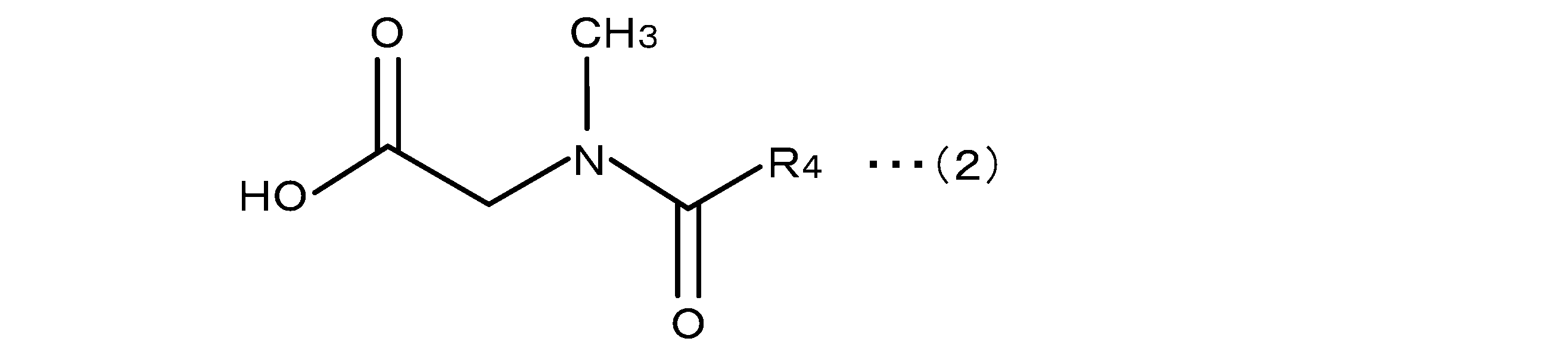
- the dispersant further contains a second dispersant which is an amino acid-based dispersant represented by the following general formula (2).
- R 4 represents a chain hydrocarbon group having 10 to 20 carbon atoms.
- the conductive powder is preferably at least one conductive powder selected from Ag, Pd, Ni, Cu, Pt, Au, and alloys thereof. It is preferable that the conductive powder is contained in an amount of 40% by mass or more and 60% by mass or less based on 100% by mass of the conductive paste.
- the average particle size of the conductive powder is preferably 0.01 ⁇ m or more and 1.0 ⁇ m or less.
- the ceramic powder contains 80% by mass or more of BaTiO 3 based on 100% by mass of the ceramic powder. Further, it is preferable that the ceramic powder be contained in an amount of 2% by mass or more and 30% by mass or less based on 100% by mass of the conductive paste. Further, it is preferable that the average particle size of the ceramic powder is 0.02 ⁇ m or more and 0.2 ⁇ m or less. Further, it is preferable that the binder resin contains at least one of a cellulose resin, an acrylic resin, and a butyral resin.
- an electronic component having a conductor formed using the conductive paste.
- a multilayer ceramic capacitor having a laminate in which an internal electrode layer formed by using a conductive paste and a dielectric layer are laminated.
- the conductive paste of the present invention because the amount of change in viscosity of the conductive paste over time is very small and excellent in adhesion, when manufacturing electronic components using the same lot of conductive paste, A conductor having the same shape and characteristics can be formed with good reproducibility irrespective of the manufacturing time, and an electronic component with small variations in product characteristics can be manufactured stably. Further, the conductive paste of the present invention has excellent adhesion to a green sheet when a laminate (compression-bonded body) is formed.
- FIGS. 1A and 1B are a perspective view and a cross-sectional view illustrating a multilayer ceramic capacitor according to an embodiment.
- the conductive paste of the present embodiment contains a conductive powder, a ceramic powder, a dispersant, a binder resin, and an organic solvent.
- a conductive powder a ceramic powder
- a dispersant a binder resin
- an organic solvent an organic solvent
- the conductive powder is not particularly limited, and a metal powder can be used.
- a metal powder can be used.
- at least one metal powder selected from Ag, Pd, Ni, Cu, Pt, Au, and an alloy thereof can be used.
- the Ni alloy for example, an alloy of at least one or more elements selected from the group consisting of Mn, Cr, Co, Al, Fe, Cu, Zn, Ag, Au, Pt, and Pd with Ni (Ni alloy) Can be used.
- the content of Ni serving as a parent phase in the Ni alloy is, for example, 50% by mass or more, and preferably 80% by mass or more.
- conductive powder such as Ni powder may contain about several hundred ppm of S in order to suppress rapid gas generation due to partial thermal decomposition of the binder resin during binder removal processing.
- the average particle size of the conductive powder is preferably 0.01 ⁇ m or more and 1.0 ⁇ m or less, more preferably 0.05 ⁇ m or more and 0.5 ⁇ m or less.
- the conductive powder can be suitably used as a paste for an internal electrode of a laminated ceramic capacitor having a reduced thickness, and for example, the smoothness of a dry film and the dry film density are improved.
- the content of the conductive powder may be, for example, 30% by mass or more and 70% by mass or less, preferably 40% by mass or more and 60% by mass or less, more preferably 100% by mass or less with respect to 100% by mass of the conductive paste. It is 40% by mass or more and 50% by mass or less. When the content of the conductive powder is in the above range, the conductivity and the dispersibility are excellent.
- the ceramic powder is not particularly limited.
- it when it is a paste for an internal electrode of a multilayer ceramic capacitor, it is appropriately selected from known ceramic powders depending on the type of the multilayer ceramic capacitor to be applied.
- the ceramic powder include a perovskite oxide containing Ba and Ti, and preferably barium titanate (BaTiO 3 ).
- BaTiO 3 barium titanate
- the content of BaTiO 3 is preferably set to 80% by mass or more based on 100% by mass of the ceramic powder.
- a ceramic powder containing barium titanate as a main component and an oxide as a subcomponent may be used.
- the oxide include oxides of Mn, Cr, Si, Ca, Ba, Mg, V, W, Ta, Nb, and one or more rare earth elements.
- a ceramic powder for example, a perovskite-type oxide ferroelectric ceramic powder in which Ba atom or Ti atom of barium titanate (BaTiO 3 ) is replaced with another atom, for example, Sn, Pb, Zr, or the like.
- a powder having the same composition as the dielectric ceramic powder constituting the green sheet of the multilayer ceramic capacitor may be used. This suppresses the occurrence of cracks due to shrinkage mismatch at the interface between the dielectric layer and the internal electrode layer in the sintering step.
- a ceramic powder other than the above include, for example, ZnO, ferrite, PZT, BaO, Al 2 O 3 , Bi 2 O 3 , R (rare earth element) 2 O 3 , TiO 2 , Nd 2 O 3 and the like. Oxides.
- One type of ceramic powder may be used, or two or more types may be used.
- the average particle size of the ceramic powder is, for example, 0.01 ⁇ m or more and 0.5 ⁇ m or less, preferably 0.02 ⁇ m or more and 0.2 ⁇ m or less, and more preferably 0.03 ⁇ m or more and 0.1 ⁇ m or less.
- the average particle diameter of the ceramic powder is in the above range, when used as an internal electrode paste, a sufficiently thin and thin uniform internal electrode can be formed.
- the average particle size of the ceramic powder is a value calculated from the specific surface area value based on the BET method.
- the content of the ceramic powder is preferably from 2% by mass to 30% by mass, more preferably from 5% by mass to 25% by mass, based on 100% by mass of the conductive paste.
- the conductivity and the dispersibility are excellent.
- the binder resin is not particularly limited, and a known resin can be used.
- the binder resin preferably contains at least one of a cellulose resin, an acrylic resin, and a butyral resin.
- the cellulose resin include methyl cellulose, ethyl cellulose, ethyl hydroxyethyl cellulose, nitrocellulose, and the like
- the butyral resin include polyvinyl butyral. Among them, it is preferable to contain ethyl cellulose from the viewpoint of solubility in a solvent, combustion decomposability, and the like.
- a butyral-based resin When used as a paste for an internal electrode, a butyral-based resin may be contained, or a butyral-based resin may be used alone from the viewpoint of improving the adhesive strength to a green sheet.
- One type of binder resin may be used, or two or more types may be used.
- the binder resin for example, a cellulose-based resin and a butyral resin can be used.
- the molecular weight of the binder resin is, for example, about 20,000 to 200,000.
- the content of the binder resin is preferably 1% by mass or more and 10% by mass or less, more preferably 3% by mass or more and 6% by mass or less based on 100% by mass of the conductive paste.
- the conductivity and the dispersibility are excellent.
- the organic solvent is not particularly limited, and a known organic solvent that can dissolve the binder resin can be used.
- the organic solvent include dihydroterpinyl acetate, isobornyl acetate, isobornyl propionate, isobornyl butyrate and isobornyl isobutyrate, ethylene glycol monobutyl ether acetate, dipropylene glycol methyl ether acetate, and the like.
- terpene solvents such as terpineol and dihydroterpineol, and hydrocarbon solvents such as tridecane, nonane and cyclohexane.
- One type of organic solvent may be used, or two or more types may be used.
- the content of the organic solvent is preferably from 20% by mass to 60% by mass, more preferably from 35% by mass to 55% by mass, based on the total amount of the conductive paste.
- the content of the organic solvent is in the above range, the conductivity and the dispersibility are excellent.
- the dispersant contains a first dispersant having an HLB value of 3.5 or more and 7.0 or less. Note that the dispersant may include a dispersant other than the first dispersant.
- the present inventors have studied various dispersants for the conductive paste, and as a result, the first dispersant having an HLB value of 3.5 or more and 7.0 or less regardless of the type of the dispersant. It has been found that, when is used, the change in viscosity of the conductive paste over time is small, and the conductive paste is excellent in viscosity stability.
- the HLB (Hydrophilic-Lipophilic Balance: hydrophilic-lipophilic balance) value is a parameter indicating the characteristics of a surfactant, is a value calculated by a known method, and takes a value from 0 to 20. Specifically, the HLB value is a value calculated by a plurality of formulas exemplified in the following (1) to (6). A low HLB value indicates high lipophilicity, and a high HLB value indicates high hydrophilicity.
- HLB 7 + 11.7 ⁇ log (Mw / Mo)
- Mw represents the sum of the atomic weights of the hydrophilic portion
- Mo represents the sum of the atomic weights of the lipophilic portion.
- HLB 7 ⁇ 4.05 ⁇ log (CMC)
- CMC represents a critical micelle concentration (mol / l).
- HLB E / 5
- E represents mass% of ethylene oxide.
- HLB 20 (1-s / A)
- s represents the saponification value of the ester
- A represents the neutralization value of the raw material fatty acid.
- HLB (E + P) / 5
- E mass% of ethylene oxide
- P mass% of polyhydric alcohol.
- HLB ⁇ (base of hydrophilic part) ⁇ ⁇ (base of lipophilic part) +7]
- the HLB In the case where the HLB is unknown, it can be determined from the HLB when the emulsified state is the same by emulsifying the oil or fat once with a certain fat or oil and then emulsifying the fat or oil with various HLB surfactants having a known HLB. it can.
- the HLB value of the first dispersant can be applied to any value calculated by any of the formulas, and is from 3.5 to 7.0.
- the HLB value of the first dispersant is in the above range, the change in the viscosity of the conductive paste over time is small, and the viscosity stability is excellent.
- the amount of coordination to various solid components such as a conductive powder and a ceramic powder becomes appropriate when the hydrophilic-lipophilic balance is within the above range. . Further, by suppressing the generation of excess dispersant, the dispersibility is improved as compared with the case where a dispersant having an HLB value outside the range of the present invention is used while having a similar structure. It is considered that the viscosity stability is further improved.
- the HLB value of the first dispersant when the HLB value of the first dispersant is less than 3.5, the lipophilicity of the dispersant becomes too high, and it becomes impossible to generate micelles and water molecules present in the paste. Inferior. When the HLB value of the first dispersant exceeds 7.0, the hydrophilicity of the dispersant becomes too high, and the wettability with the filler is deteriorated.
- a dispersant having an HLB value within the above range can be used without particular limitation.
- an amine-based dispersant represented by the following general formula (1) is a tertiary amine or a secondary amine, and has a structure in which an amine group is bonded to one or two polyoxyethylene groups.
- R 1 represents an alkyl group, an alkenyl group, or an alkynyl group having 8 to 16 carbon atoms
- R 2 represents an oxyethylene group, an oxypropylene group, or a methylene group
- 3 represents an oxyethylene group or an oxypropylene group
- R 2 and R 3 may be the same or different, and the N atom in the formula (1) and R 2 and R 3 (It is not directly bonded to the O atom therein, and Y is a number from 0 to 2 and Z is a number from 1 to 2.)
- R 1 represents an alkyl group having 8 to 16 carbon atoms, an alkenyl group, or an alkynyl group.
- the powder in the conductive paste has sufficient dispersibility and is excellent in solubility in a solvent.
- R 1 is preferably a straight-chain hydrocarbon group.
- R 2 represents an oxyethylene group, an oxypropylene group or a methylene group
- R 3 represents an oxyethylene group or an oxypropylene group
- R 2 and R 3 are the same even if they are the same. Or may be different.
- the N atom in the formula (1) and the O atom in R 2 and R 3 are not directly bonded
- Y is a number of 0 or more and 2
- Z is a number of 1 or more and 2 or less.
- R 2 is an oxyalkylene group represented by — (AO) Y —
- the O atom in the oxyalkylene group bonds to an H atom adjacent to R2.
- R2 is a methylene group
- R2 is represented by — (CH 2 ) Y —
- Y is 1-2
- R 3 is an oxyalkylene group represented by — (AO) z —
- an O atom in the oxyalkylene group is bonded to an H atom adjacent to R 3 .
- the amine-based dispersant when Y is 0, is a secondary amine having an alkyl group, an alkenyl group, or an alkynyl group having 8 to 16 carbon atoms and one hydrogen group.
- the amine-based dispersant when Y is 0 and Z is 2, includes an alkyl group, an alkenyl group, or an alkynyl group having 8 to 16 carbon atoms, one hydrogen group, and one polyoxyethylene group. Or, it becomes a secondary amine composed of a polyoxypropylene group.
- the amine-based dispersant is a tertiary amine having an alkyl group, an alkenyl group, or an alkynyl group having 8 to 16 carbon atoms.
- the amine-based dispersant includes an alkyl, alkenyl, or alkynyl group having 8 to 16 carbon atoms and a tertiary amine having at least one polyoxyethylene group or polyoxypropylene group.
- the amine-based dispersant represented by the above formula (1) for example, a commercially available product that satisfies the above characteristics can be used. Further, the amine-based dispersant may be manufactured so as to satisfy the above characteristics by using a conventionally known manufacturing method.
- the first dispersant is contained in an amount of 0.4% by mass or more and 1% by mass or less based on 100% by mass of the conductive paste.
- the content of the first dispersant is less than 0.4% by mass, the conductive powder cannot be uniformly dispersed, the conductive powder is aggregated, the dry film density does not increase, and the viscosity does not increase. May not be able to suppress changes over time.
- the content of the first dispersant exceeds 1% by mass, an excessive dispersant remains on the surface of the dried film, hinders the adhesion between the surface of the dried film and the surface of the green sheet during lamination and press-bonding, and causes peeling. There are cases.
- the dispersant used in the present embodiment further preferably contains an amino acid-based dispersant represented by the following general formula (2) as the second dispersant in addition to the first dispersant.
- the second dispersant has an N-acylamino acid skeleton and has a chain hydrocarbon group having 10 to 20 carbon atoms.
- R 4 represents a chain hydrocarbon group having 10 to 20 carbon atoms.
- R 4 represents a chain hydrocarbon group having 10 to 20 carbon atoms.
- R 4 preferably has 15 to 20 carbon atoms.
- the chain hydrocarbon group may be a straight-chain hydrocarbon group or a branched hydrocarbon group.
- the chain hydrocarbon group may be an alkyl group, an alkenyl group, or an alkynyl group.
- R 4 is preferably a straight-chain hydrocarbon group, more preferably a straight-chain alkenyl group, and has a double bond.
- the conductive paste according to the present embodiment can further suppress the change with time in viscosity by further including the second dispersant, that is, the amino acid-based dispersant represented by the above formula (2). Therefore, the conductive paste containing the first dispersant and the second dispersant can be suitably used particularly for electronic components that require high-definition printing.
- the second dispersant for example, a product that satisfies the above characteristics can be selected from commercially available products and used.
- the second dispersant may be manufactured using a conventionally known manufacturing method so as to satisfy the above characteristics.
- the total content of the dispersant is 0.4% by mass or more and 2% by mass or less based on 100% by mass of the conductive paste. Yes, it may be 0.4% by mass or more and 1.5% by mass or less.
- the first dispersant and the second dispersant are considered to have different main dispersion targets, and the dispersibility is improved when the total content of the dispersants is in the range of 0.4% by mass or more and 2% by mass or less.
- the amount of change in viscosity can be suppressed low.
- the total content of the dispersant is less than 0.4% by mass, the effect of the dispersant may not be sufficiently obtained. If the total content of the dispersant exceeds 2% by mass, an excessive amount of the dispersant remains on the dried film surface, hinders the adhesion between the conductive film surface and the green sheet surface during lamination, and causes peeling. May not be formed.
- the viscosity of the conductive paste can be adjusted to an appropriate range, and the sheet attack and the green sheet can be adjusted. Can be prevented from peeling off.
- the conductive paste of the present invention may contain a dispersant other than the first and second dispersants as long as the effects of the present invention are not impaired.
- dispersants other than those described above include, for example, acid dispersants including higher fatty acids, polymer surfactants, cationic dispersants other than acid dispersants, nonionic dispersants, amphoteric surfactants, and polymer dispersants. It may contain a dispersant or the like. These dispersants may be used alone or in combination of two or more.
- the conductive paste of the present embodiment may include other components other than the above components as necessary.
- additives such as an antifoaming agent, a plasticizer, a surfactant, and a thickener can be used.
- the method for producing the conductive paste of the present embodiment is not particularly limited, and a conventionally known method can be used.
- the conductive paste can be produced, for example, by stirring and kneading the above components with a ball mill, a bead mill, a three-roll mill, a mixer, or the like. At this time, if the dispersant is applied to the surface of the conductive powder in advance, the conductive powder is sufficiently loosened without agglomeration, and the dispersant spreads over the surface, so that a uniform conductive paste can be easily obtained.
- the conductive powder, the ceramic powder, the organic vehicle and the dispersant are added to the organic solvent for paste adjustment, and then stirred.
- the conductive paste may be prepared by kneading.
- the viscosity of the conductive paste after 24 hours of production of the conductive paste is a reference (0%)
- the viscosity after standing for 110 days from the reference date is preferably within ⁇ 40%.
- the conductive paste can be suitably used for electronic components such as multilayer ceramic capacitors.
- the multilayer ceramic capacitor has a dielectric layer formed using a dielectric green sheet and an internal electrode layer formed using a conductive paste.
- the dielectric ceramic powder contained in the dielectric green sheet and the ceramic powder contained in the conductive paste have the same composition.
- the multilayer ceramic capacitor manufactured using the conductive paste of the present embodiment even when the thickness of the dielectric green sheet is, for example, 3 ⁇ m or less, sheet attack and defective peeling of the green sheet are suppressed.
- FIGS. 1A and 1B are views showing a multilayer ceramic capacitor 1 which is an example of an electronic component according to an embodiment.
- the multilayer ceramic capacitor 1 includes a multilayer body 10 in which dielectric layers 12 and internal electrode layers 11 are alternately stacked, and external electrodes 20.
- a method for manufacturing a multilayer ceramic capacitor using the conductive paste will be described.
- a conductive paste is printed on a dielectric layer made of a green sheet and dried to form a dried film.
- the laminated body is baked and integrated to form the internal electrode layer 11 and the dielectric layer.
- a ceramic laminated body 10 laminated body 10 in which 12 and 12 are alternately laminated is produced.
- a pair of external electrodes 20 is formed on both ends of the ceramic laminate 10 to manufacture the multilayer ceramic capacitor 1. The details will be described below.
- a green sheet which is an unfired ceramic sheet.
- a dielectric layer paste obtained by adding an organic binder such as polyvinyl butyral and a solvent such as terpineol to raw material powder of a predetermined ceramic such as barium titanate is supported on a PET film or the like. Examples thereof include those coated on a film in a sheet form and dried to remove the solvent.
- the thickness of the dielectric layer made of a green sheet is not particularly limited, but is preferably 0.05 ⁇ m or more and 3 ⁇ m or less from the viewpoint of demand for miniaturization of the multilayer ceramic capacitor.
- the above-mentioned conductive paste is printed (applied) on one surface of the green sheet by a known method such as a screen printing method and dried, and a plurality of dried sheets are prepared.
- the thickness of the conductive paste (dry film) after printing is preferably 1 ⁇ m or less after drying from the viewpoint of a demand for thinning the internal electrode layer 11.
- the green sheet is peeled off from the supporting film, and the dielectric layer composed of the green sheet and the dry film formed on one surface thereof are laminated so as to be alternately arranged. Get. Note that a configuration may be adopted in which protective green sheets to which the conductive paste is not applied are further disposed on both surfaces of the laminate.
- the green chip is subjected to a binder removal treatment and fired in a reducing atmosphere to produce the ceramic laminate 10.
- the atmosphere in the binder removal treatment is preferably air or an N 2 gas atmosphere.
- the temperature at the time of performing the binder removal treatment is, for example, 200 ° C. or more and 400 ° C. or less.
- the holding time of the above-mentioned temperature when performing the binder removal treatment is 0.5 hours or more and 24 hours or less.
- the firing is performed in a reducing atmosphere in order to suppress the oxidation of the metal used for the internal electrode layer.
- the firing temperature of the stacked body is, for example, 1000 ° C. or more and 1350 ° C. or less.
- the temperature holding time at the time of performing is, for example, 0.5 hours or more and 8 hours or less.
- the organic binder in the green sheet is completely removed, and the ceramic raw material powder is fired to form the ceramic dielectric layer 12.
- the organic vehicle in the dried film is removed, and the nickel powder or the alloy powder containing nickel as a main component is sintered or melted and integrated to form an internal electrode, and the dielectric layer 12 and the internal electrode layer 11 are formed.
- the fired multilayer ceramic fired body may be annealed from the viewpoint of improving reliability by taking oxygen into the dielectric layer and suppressing re-oxidation of the internal electrode.
- the multilayer ceramic capacitor 1 is manufactured by providing a pair of external electrodes 20 to the manufactured multilayer ceramic fired body.
- the external electrode 20 includes an external electrode layer 21 and a plating layer 22.
- External electrode layer 21 is electrically connected to internal electrode layer 11.
- a material of the external electrode 20 for example, copper, nickel, or an alloy thereof can be preferably used.
- the electronic component is not limited to the multilayer ceramic capacitor, but may be an electronic component other than the multilayer ceramic capacitor.
- Ceramic powder As the ceramic powder, commercially available barium titanate (BaTiO 3 ) having an average particle diameter of 0.1 ⁇ m was used.
- Binder resin As the binder resin, a commercially available ethyl cellulose resin (STD-100 manufactured by Dow Chemical Company) was used.
- a dispersant B represented by R 4 CC 17 H 33 (straight chain hydrocarbon group) in the general formula (2) was used.
- Organic solvent As the organic solvent, a mixture of isobornyl acetate and ethylene glycol monobutyl ether acetate was used.
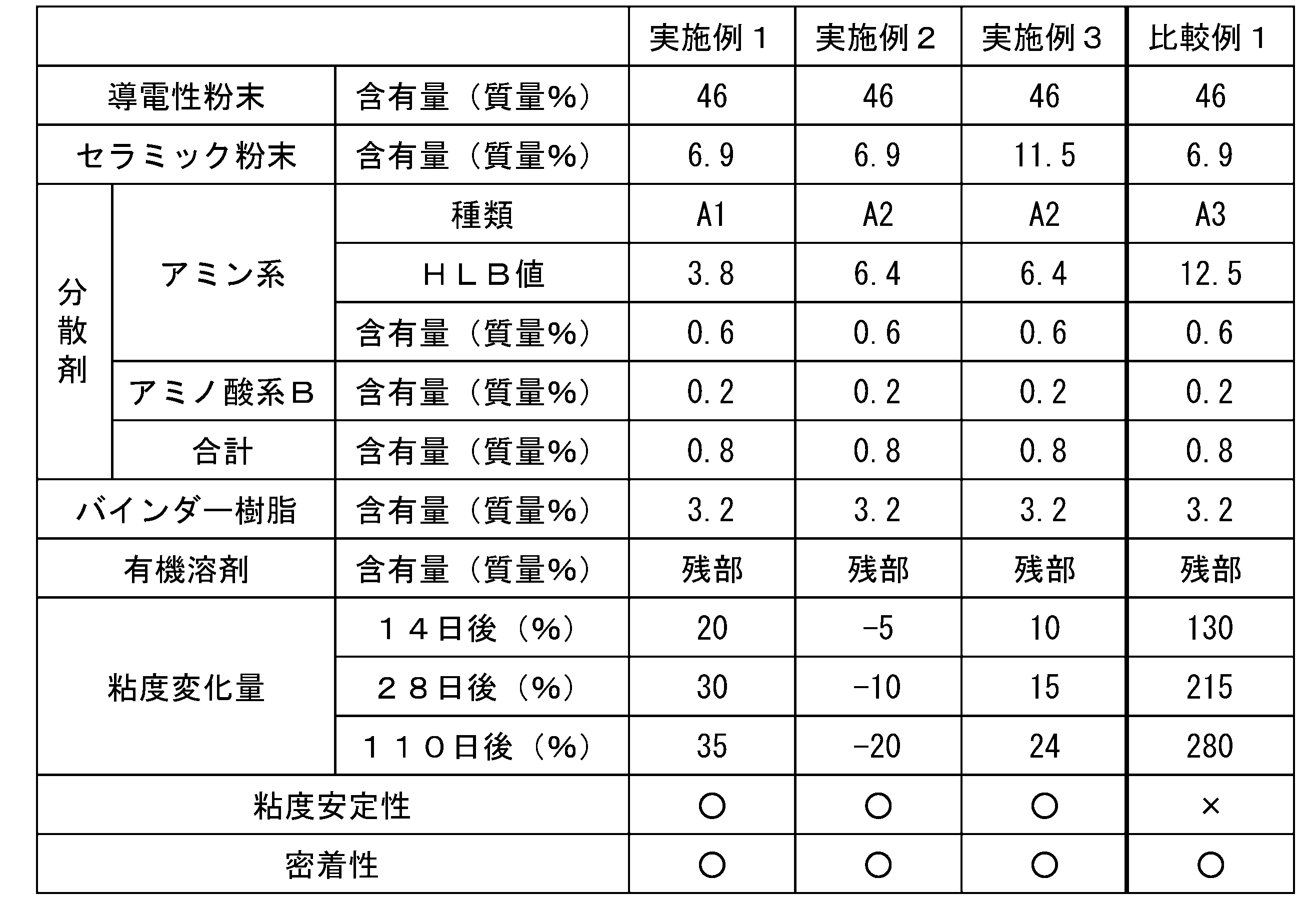
- Example 1 46% by mass of Ni powder, 6.9% by mass of ceramic powder, 3.2% by mass of binder resin in vehicle, 0.6% by mass of amine-based dispersant (dispersant A1), amino acid-based dispersant (dispersant B) was added, and an organic solvent was added as a balance, and the resulting mixture was blended so as to be 100% by mass as a whole. These materials were mixed to prepare a conductive paste. The viscosity stability and adhesion of the prepared conductive paste were evaluated by the following methods. Table 1 shows the evaluation results.
- the viscosity stability of the conductive paste was evaluated as “O” when the amount of change in the viscosity of the conductive paste after standing for 110 days was 40% or less, and “X” when the amount exceeded 40%.
- the prepared conductive paste was printed (applied) on a green sheet by a screen printing method, and dried to prepare a plurality of sheets each having a dried film formed on the green sheet. Five of these sheets were laminated and subjected to a thermocompression treatment at 80 ° C. under a pressure of 100 kg / cm 2 for 3 minutes to form a laminate (compression-bonded body). In the obtained laminate, the adhesion was evaluated according to the following criteria.
- Example 2 A conductive paste was prepared under the same conditions as in Example 1 except that Dispersant A2 was used as the amine-based dispersant. The viscosity stability and adhesiveness of the prepared conductive paste were evaluated by the above methods. Table 1 shows the evaluation results.
- Example 3 A conductive paste was produced under the same conditions as in Example 2 except that the content of the ceramic powder was 11.5% by mass. The viscosity stability and adhesiveness of the prepared conductive paste were evaluated by the above methods. Table 1 shows the evaluation results.
- Example 1 A conductive paste was prepared under the same conditions as in Example 1 except that Dispersant A3 was used as the amine-based dispersant. The viscosity stability and adhesiveness of the prepared conductive paste were evaluated by the above methods. Table 1 shows the evaluation results.
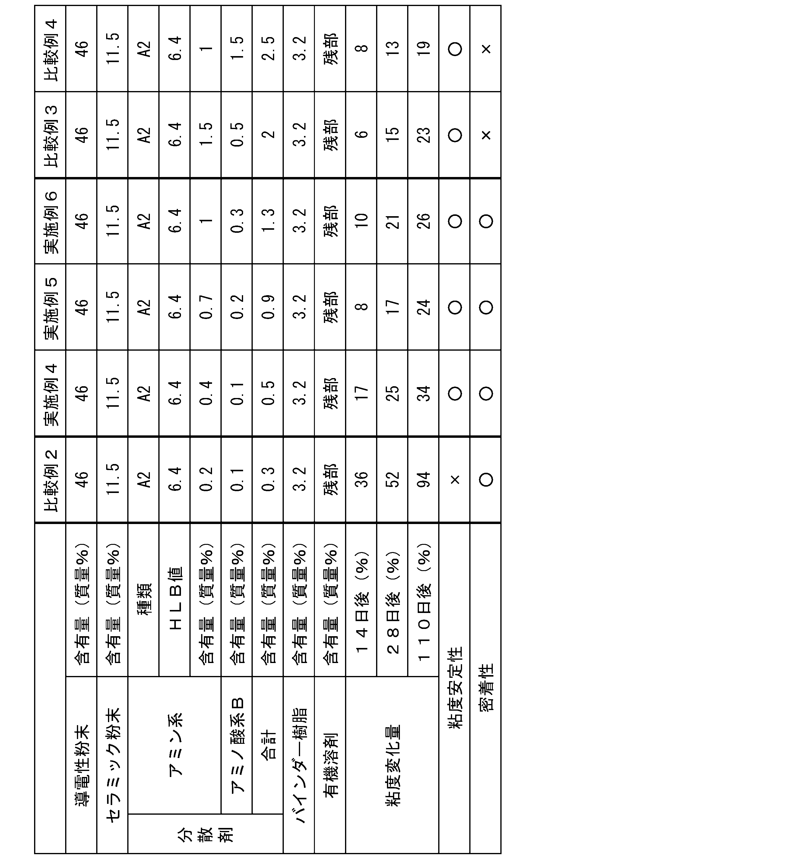
- Examples 4 to 6, Comparative Examples 2 to 4 A conductive paste was produced under the same conditions as in Example 3 except that the contents of the amine dispersant and the amino acid dispersant were changed as shown in Table 2. The amount of change in viscosity, the dry film density, the surface roughness of the dry film, and the adhesion of the prepared conductive paste were evaluated by the above-described methods. Table 2 shows the evaluation results.
- the conductive paste of Comparative Example 1 in which the HLB value is higher than the range of the present invention is inferior in viscosity stability, the viscosity change after 14 days is greatly changed to 130%, and after 110 days, 280%, which indicates that it is difficult to form a conductor under the same manufacturing conditions.
- the conductive paste of Comparative Example 2 in which the content of the amine-based dispersant was smaller than the range of the present invention had low dispersibility of the constituent materials and was inferior in viscosity stability, and the viscosity change after 14 days was 36%. It can be seen that the change in viscosity after 110 days is 94%, and the change in viscosity is large.
- the conductive paste of Comparative Example 3 in which the content of the amine-based dispersant is larger than the range of the present invention and Comparative Example 4 in which the total content of the dispersant is larger than the range of the present invention show that the excess dispersant component is present on the conductor surface. Remaining, peeling occurred in the manufactured laminate, and the adhesion was reduced.
- the conductive paste according to the present embodiment is excellent in dispersibility, very excellent in viscosity stability over time, and has sufficient adhesion in the laminate, so that the production timing in the same lot Even if there is a difference between the products, it is possible to manufacture products in almost the same state under the same manufacturing conditions with a high yield. Therefore, the conductive paste according to the present embodiment can be suitably used as a raw material for an internal electrode of a multilayer ceramic capacitor, which is an electronic component particularly used in electronic devices such as mobile phones and digital devices.
Landscapes
- Engineering & Computer Science (AREA)
- Power Engineering (AREA)
- Chemical & Material Sciences (AREA)
- Manufacturing & Machinery (AREA)
- Microelectronics & Electronic Packaging (AREA)
- Spectroscopy & Molecular Physics (AREA)
- Physics & Mathematics (AREA)
- Dispersion Chemistry (AREA)
- Inorganic Chemistry (AREA)
- Ceramic Engineering (AREA)
- Ceramic Capacitors (AREA)
- Conductive Materials (AREA)
- Fixed Capacitors And Capacitor Manufacturing Machines (AREA)
Abstract
経時的な粘度変化が非常に少なく、粘度安定性により優れ、かつ、積層体を形成した際にグリーンシートとの密着性に優れた導電性ペーストを提供する。 導電性粉末、セラミック粉末、分散剤、バインダー樹脂、及び有機溶剤を含む導電性ペーストであって、分散剤が3.5以上7.0以下のHLB値を有する第1の分散剤を含有し、第1の分散剤を、導電性ペースト100質量%に対して、0.4質量%以上1質量%以下含有し、かつ、分散剤を、導電性ペースト100質量%に対して、総含有量で0.4質量%以上2質量%以下含有することを特徴とする導電性ペースト。
Description
本発明は導電性ペースト、及びその導電性ペーストを用いて形成された電子部品及び積層セラミックコンデンサに関する。
電子部品の軽薄短小化が進み、電子部品の一種である積層セラミックコンデンサについても小型、大容量化の要求がますます高まりつつある。積層セラミックコンデンサは、複数の誘電体層と複数の内部電極層とが交互に積層した構造を有しており、内部電極層と誘電体層を薄くすることにより、積層セラミックコンデンサの小型、大容量化を図ることができる。
積層セラミックコンデンサは、例えば、次のような工程を経て製造される。まず、チタン酸バリウム(BaTiO3)等の誘電体粉末と、ポリビニルブチラール、アクリル等の有機バインダーとを含有するグリーンシートの表面上に、導電粉末を含有する内部電極用の導電性ペーストを所定のパターンで印刷し、これを乾燥して乾燥膜を形成する。次に、乾燥膜とグリーンシートとが交互に重なるよう、乾燥膜を有するグリーンシートを積層した後、熱圧着し、圧着体を形成する。この圧着体を目的の大きさに切断した後、所定の温度および雰囲気で脱バインダー処理を行い、続いて内部電極と誘電体の焼結を目的として焼成する。焼成後に得られる素体の両端部に、積層セラミックコンデンサと外部デバイスを接合するための外部電極を取り付け、積層セラミックコンデンサを得る。
内部電極用の導電性ペーストは、例えば、導電性粉末、セラミック粉末、有機バインダー樹脂、有機溶剤を含む。さらに、導電性ペーストに所定のレオロジー特性を付与し、無機物の安定分散を行わせる目的で有機添加剤等を含有させてもよい。これらの材料は、例えば、ボールミル、ビーズミル、3本ロールミル等によって分散処理され、最終的に目的の粘度に合わせ込むため希釈剤と呼ばれる有機溶剤が加えられて完成する。希釈剤に用いる有機溶剤は、導電性ペースト作製時に使用した有機溶剤と同じものを用いても良いし、別の有機溶剤を用いても良い。
近年の電子部品の小型化による、内部電極の薄膜化に伴い、導電性粉末も小粒径化する傾向がある。導電性粉末の粒径が小さくなると、その粒子表面の比表面積が大きくなるため、導電性粉末の表面活性が高くなり、導電性ペーストの分散性の低下や、粘度特性の低下を生じてしまったり、その粘度が経時的に変化してしまったりする場合がある。
そこで、導電性ペーストの経時的な粘度特性の改善の試みがなされている。例えば、特許文献1には、少なくとも金属成分と、酸化物と、分散剤と、バインダー樹脂とを含有する導電性ペーストであって、金属成分は、その表面組成が、特定の組成比を有するNi粉末であり、分散剤の酸点量は、500~2000μmol/gであり、バインダー樹脂の酸点量は、15~100μmol/gである導電性ペーストが記載されている。そして、特許文献1によれば、この導電性ペーストは、良好な分散性と粘度安定性を有するとされている。
また、特許文献2には、導電性粉末、樹脂、有機溶剤、TiBaO3を主とするセラミックス粉末の共材、および凝集抑制剤からなる内部電極用導電ペーストであって、前記凝集抑制剤の含有量が0.1重量%以上5重量%以下であり、前記凝集抑制剤が、特定の構造式で示される3級アミン又は2級アミンである内部電極用導電ペーストが記載されている。特許文献2によれば、この内部電極用導電ペーストは、共材成分の凝集を抑制し、長期保管性に優れ、積層セラミックコンデンサの薄膜化が可能とされている。
しかしながら、近年の電子部品の小型化による内部電極の薄膜化に伴い、印刷精度にも高い精度が要求されつつあり、印刷時期の差による変化が極力起きない様、経時的な粘度特性のさらなる安定性向上が求められている。
本発明は、この様な状況に鑑み、経時的な粘度変化が非常に少なく、粘度安定性により優れ、かつ、積層体(圧着体)を形成した際にグリーンシートとの密着性に優れた導電性ペーストを提供することを目的としている。
本発明の第1の態様では、導電性粉末、セラミック粉末、分散剤、バインダー樹脂、及び有機溶剤を含む導電性ペーストであって、分散剤が3.5以上7.0以下のHLB値を有する第1の分散剤を含有し、第1の分散剤を、導電性ペースト100質量%に対して、0.4質量%以上1質量%以下含有し、かつ、分散剤を、導電性ペースト100質量%に対して、総含有量で0.4質量%以上2質量%以下含有することを特徴とする導電性ペーストが提供される。
また、第1の分散剤が、下記一般式(1)で示されるアミン系分散剤であることが好ましい。

(ただし、式(1)中、R1は炭素数8~16のアルキル基、アルケニル基、又は、アルキニル基を表し、R2はオキシエチレン基、オキシプロピレン基、又は、メチレン基を表し、R3はオキシエチレン基、又は、オキシプロピレン基を表し、R2及びR3は、同一でもよく、又は、異なっていてもよい。また、式(1)中のN原子と、R2及びR3中のO原子とは直接結合せず、かつ、Yは0~2の数であり、Zは1~2の数である。)
また、分散剤が、下記一般式(2)で示されるアミノ酸系分散剤である第2の分散剤を更に含有することが好ましい。
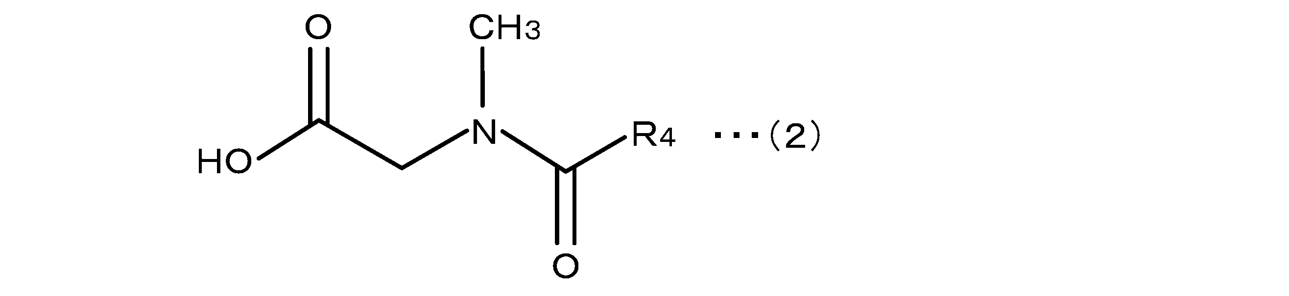
また、導電性粉末が、Ag、Pd、Ni、Cu、Pt、Au及びこれらの合金の中から選ばれる1種以上の導電性粉末であることが好ましい。また、導電性粉末を、導電性ペースト100質量%に対して、40質量%以上60質量%以下含有することが好ましい。また、導電性粉末の平均粒径が、0.01μm以上1.0μm以下であることが好ましい。
また、セラミック粉末が、セラミック粉末100質量%に対して、BaTiO3を80質量%以上含有することが好ましい。また、セラミック粉末を、導電性ペースト100質量%に対して、2質量%以上30質量%以下含有することが好ましい。また、セラミック粉末の平均粒径が0.02μm以上0.2μm以下であることが好ましい。また、バインダー樹脂が、セルロース系樹脂、アクリル系樹脂、及びブチラール系樹脂のうち少なくとも1種を含有することが好ましい。
本発明の第2の態様では、上記導電性ペーストを用いて形成した導体を有することを特徴とする電子部品が提供される。
本発明の第3の態様では、導電性ペーストを用いて形成した内部電極層と誘電体層とを積層した積層体を有することを特徴とする積層セラミックコンデンサが提供される。
本発明の導電性ペーストを用いて形成された電子部品は、導電性ペーストの粘度経時変化量が非常に少なく密着性に優れるため、同一ロットの導電性ペーストを用いて電子部品を製造する場合、その製造時期に依らず、再現性良く同じ形状、特性を有する導体を形成することができ、製品特性においてもバラツキの小さい電子部品を安定して製造することができる。また、本発明の導電性ペーストは、積層体(圧着体)を形成した際にグリーンシートとの密着性に優れる。
本実施形態の導電性ペーストは、導電性粉末、セラミック粉末、分散剤、バインダー樹脂及び有機溶剤を含む。以下、各成分について詳細に説明する。
(導電性粉末)
導電性粉末は、特に限定されず、金属粉末を用いることができ、例えば、Ag、Pd、Ni、Cu、Pt、Au、及びこれらの合金から選ばれる少なくとも1種の金属粉末を用いることができる。これらの中でも、導電性、耐食性及びコストの観点から、Ni、またはその合金の粉末を用いるのが好ましい。Ni合金としては、例えば、Mn、Cr、Co、Al、Fe、Cu、Zn、Ag、Au、PtおよびPdからなる群より選択される少なくとも1種以上の元素とNiとの合金(Ni合金)を用いることができる。Ni合金における母相となるNiの含有量は、例えば、50質量%以上、好ましくは80質量%以上である。また、Ni粉末等の導電性粉末は、脱バインダー処理の際、バインダー樹脂の部分的な熱分解による急激なガス発生を抑制するために、数百ppm程度のSを含んでもよい。
導電性粉末は、特に限定されず、金属粉末を用いることができ、例えば、Ag、Pd、Ni、Cu、Pt、Au、及びこれらの合金から選ばれる少なくとも1種の金属粉末を用いることができる。これらの中でも、導電性、耐食性及びコストの観点から、Ni、またはその合金の粉末を用いるのが好ましい。Ni合金としては、例えば、Mn、Cr、Co、Al、Fe、Cu、Zn、Ag、Au、PtおよびPdからなる群より選択される少なくとも1種以上の元素とNiとの合金(Ni合金)を用いることができる。Ni合金における母相となるNiの含有量は、例えば、50質量%以上、好ましくは80質量%以上である。また、Ni粉末等の導電性粉末は、脱バインダー処理の際、バインダー樹脂の部分的な熱分解による急激なガス発生を抑制するために、数百ppm程度のSを含んでもよい。
導電性粉末の平均粒径は、好ましくは0.01μm以上1.0μm以下であり、より好ましくは0.05μm以上0.5μm以下である。導電性粉末の平均粒径が上記範囲である場合、薄膜化した積層セラミックコンデンサの内部電極用ペーストとして好適に用いることができ、例えば、乾燥膜の平滑性及び乾燥膜密度が向上する。
導電性粉末の平均粒径は、BET法に基づいて比表面積値から算出した値である。算出式は次の通りである。
平均粒径=6/S.A×ρ
(ρ:各粉末の真密度(ニッケルの場合は8.9)、S.A:各粉末の比表面積値)
平均粒径=6/S.A×ρ
(ρ:各粉末の真密度(ニッケルの場合は8.9)、S.A:各粉末の比表面積値)
導電性粉末の含有量は、導電性ペースト100質量%に対して、例えば、30質量%以上70質量%以下であってもよく、好ましくは40質量%以上60質量%以下であり、より好ましくは40質量%以上50質量%以下である。導電性粉末の含有量が上記範囲である場合、導電性及び分散性に優れる。
(セラミック粉末)
セラミック粉末としては、特に限定されず、例えば、積層セラミックコンデンサの内部電極用ペーストである場合、適用する積層セラミックコンデンサの種類により適宜、公知のセラミック粉末から選択される。セラミック粉末としては、例えば、Ba及びTiを含むペロブスカイト型酸化物が挙げられ、好ましくはチタン酸バリウム(BaTiO3)である。なお、セラミック粉末としてBaTiO3を用いる場合は、セラミック粉末100質量%に対してBaTiO3の含有量を80質量%以上とするのが好ましい。
セラミック粉末としては、特に限定されず、例えば、積層セラミックコンデンサの内部電極用ペーストである場合、適用する積層セラミックコンデンサの種類により適宜、公知のセラミック粉末から選択される。セラミック粉末としては、例えば、Ba及びTiを含むペロブスカイト型酸化物が挙げられ、好ましくはチタン酸バリウム(BaTiO3)である。なお、セラミック粉末としてBaTiO3を用いる場合は、セラミック粉末100質量%に対してBaTiO3の含有量を80質量%以上とするのが好ましい。
セラミック粉末としては、チタン酸バリウムを主成分とし、酸化物を副成分として含むセラミック粉末を用いてもよい。酸化物としては、Mn、Cr、Si、Ca、Ba、Mg、V、W、Ta、Nbおよび1種類以上の希土類元素の酸化物が挙げられる。このようなセラミック粉末としては、例えば、チタン酸バリウム(BaTiO3)のBa原子やTi原子を他の原子、例えば、Sn、Pb、Zrなどで置換したペロブスカイト型酸化物強誘電体のセラミック粉末が挙げられる。
内部電極用ペーストにおいては、積層セラミックコンデンサのグリーンシートを構成する誘電体セラミック粉末と同一組成の粉末を用いてもよい。これにより、焼結工程における誘電体層と内部電極層との界面での収縮のミスマッチによるクラック発生が抑制される。このようなセラミック粉末としては、上記以外に、例えば、ZnO、フェライト、PZT、BaO、Al2O3、Bi2O3、R(希土類元素)2O3、TiO2、Nd2O3などの酸化物が挙げられる。なお、セラミック粉末は、1種類を用いてもよく、2種類以上を用いてもよい。
セラミック粉末の平均粒径は、例えば、0.01μm以上0.5μm以下であり、好ましくは0.02μm以上0.2μm以下であり、より好ましくは0.03μm以上0.1μm以下の範囲である。セラミック粉末の平均粒径が上記範囲であることにより、内部電極用ペーストとして用いた場合、十分に細く薄い均一な内部電極を形成することができる。
セラミック粉末の平均粒径は、BET法に基づいて比表面積値から算出した値である。算出式は次の通りである。
平均粒径=6/S.A×ρ
(ρ:各粉末の真密度(チタン酸バリウムの場合は6.1)、S.A:各粉末の比表面積値)
平均粒径=6/S.A×ρ
(ρ:各粉末の真密度(チタン酸バリウムの場合は6.1)、S.A:各粉末の比表面積値)
セラミック粉末の含有量は、導電性ペースト100質量%に対して、好ましくは2質量%以上30質量%以下であり、より好ましくは5質量%以上25質量%以下である。導電性粉末の含有量が上記範囲である場合、導電性及び分散性に優れる。
(バインダー樹脂)
バインダー樹脂としては、特に限定されず、公知の樹脂を用いることができる。バインダー樹脂としては、セルロース系樹脂、アクリル系樹脂、及びブチラール系樹脂のうち少なくとも1種を含有することが好ましい。セルロース系樹脂としては、例えば、メチルセルロース、エチルセルロース、エチルヒドロキシエチルセルロース、ニトロセルロースなどが挙げられ、ブチラール系樹脂としては、ポリビニルブチラールなどが挙げられる。中でも、溶剤への溶解性、燃焼分解性の観点などからエチルセルロースを含むことが好ましい。また、内部電極用ペーストとして用いる場合、グリーンシートとの接着強度を向上させる観点からブチラール系樹脂を含む、又は、ブチラール系樹脂を単独で使用してもよい。バインダー樹脂は、1種類を用いてもよく、又は、2種類以上を用いてもよい。バインダー樹脂は、例えば、セルロース系の樹脂とブチラール樹脂とを用いることができる。また、バインダー樹脂の分子量は、例えば、20000~200000程度である。
バインダー樹脂としては、特に限定されず、公知の樹脂を用いることができる。バインダー樹脂としては、セルロース系樹脂、アクリル系樹脂、及びブチラール系樹脂のうち少なくとも1種を含有することが好ましい。セルロース系樹脂としては、例えば、メチルセルロース、エチルセルロース、エチルヒドロキシエチルセルロース、ニトロセルロースなどが挙げられ、ブチラール系樹脂としては、ポリビニルブチラールなどが挙げられる。中でも、溶剤への溶解性、燃焼分解性の観点などからエチルセルロースを含むことが好ましい。また、内部電極用ペーストとして用いる場合、グリーンシートとの接着強度を向上させる観点からブチラール系樹脂を含む、又は、ブチラール系樹脂を単独で使用してもよい。バインダー樹脂は、1種類を用いてもよく、又は、2種類以上を用いてもよい。バインダー樹脂は、例えば、セルロース系の樹脂とブチラール樹脂とを用いることができる。また、バインダー樹脂の分子量は、例えば、20000~200000程度である。
バインダー樹脂の含有量は、導電性ペースト100質量%に対して、好ましくは1質量%以上10質量%以下であり、より好ましくは3質量%以上6質量%以下である。バインダー樹脂の含有量が上記範囲である場合、導電性及び分散性に優れる。
(有機溶剤)
有機溶剤としては、特に限定されず、上記バインダー樹脂を溶解することができる公知の有機溶剤を用いることができる。有機溶剤としては、例えば、ジヒドロターピニルアセテート、イソボルニルアセテート、イソボルニルプロピネート、イソボルニルブチレート及びイソボルニルイソブチレート、エチレングリコールモノブチルエーテルアセテート、ジプロピレングリコールメチルエーテルアセテートなどのアセテート系溶剤、ターピネオール、ジヒドロターピネオールなどのテルペン系溶剤、トリデカン、ノナン、シクロヘキサンなどの炭化水素系溶剤などが挙げられる。なお、有機溶剤は、1種類を用いてもよく、2種類以上を用いてもよい。
有機溶剤としては、特に限定されず、上記バインダー樹脂を溶解することができる公知の有機溶剤を用いることができる。有機溶剤としては、例えば、ジヒドロターピニルアセテート、イソボルニルアセテート、イソボルニルプロピネート、イソボルニルブチレート及びイソボルニルイソブチレート、エチレングリコールモノブチルエーテルアセテート、ジプロピレングリコールメチルエーテルアセテートなどのアセテート系溶剤、ターピネオール、ジヒドロターピネオールなどのテルペン系溶剤、トリデカン、ノナン、シクロヘキサンなどの炭化水素系溶剤などが挙げられる。なお、有機溶剤は、1種類を用いてもよく、2種類以上を用いてもよい。
電子部品の小型化に伴い、誘電体層を形成するグリーンシートが薄層化するに従い、導電性ペーストに含まれる有機溶剤が浸透するシートアタックが問題になる場合がある。この様な場合には、有機溶剤として、エチレングリコールモノブチルエーテルアセテート、又はジプロピレングリコールメチルエーテルアセテートから選ばれる少なくとも一種を用いるのが好ましい。また、更にジヒドロターピニルアセテート、イソボルニルプロピオネート、イソボルニルブチレート、又はイソボルニルイソブチレートから選ばれる少なくとも一種を混合して用いるのが好ましい。
有機溶剤の含有量は、導電性ペースト全量に対して、20質量%以上60質量%以下が好ましく、35質量%以上55質量%以下がより好ましい。有機溶剤の含有量が上記範囲である場合、導電性及び分散性に優れる。
(分散剤)
分散剤は、HLB値が3.5以上7.0以下である第1の分散剤を含有する。なお、分散剤は、第1の分散剤以外の分散剤を含んでもよい。
分散剤は、HLB値が3.5以上7.0以下である第1の分散剤を含有する。なお、分散剤は、第1の分散剤以外の分散剤を含んでもよい。
本発明者らは、導電性ペーストに用いる分散剤について、種々の分散剤を検討した結果、分散剤の種類に依らず、HLB値が3.5以上7.0以下である第1の分散剤を用いた場合に、導電性ペーストの経時的な粘度変化が少なく、粘度安定性に優れることを見出した。
HLB(Hydrophilic-Lipophilic Balance:親水性-親油性バランス)値は、界面活性剤の特性を示すパラメータで、公知の方法により算出される値であり、0から20までの値をとる。具体的には、HLB値は、下記(1)~(6)に例示する複数の計算式で算出される値である。HLB値が低い値の場合は親油性が高いことを示し、HLB値が高い場合は親水性が高いことを示す。
(1)HLB=7+11.7×log(Mw/Mo)
上記式中、Mw:親水性部の原子量の和、Mo:親油性部の原子量の和を表す。
(2)HLB=7-4.05×log(CMC)
上記式中、CMC:臨界ミセル濃度(mol/l)を表す。
(3)1価アルコールのエチレンオキシド誘導体の場合:
HLB=E/5
上記式中、E:エチレンオキシドの質量%を表す。
(4)多価アルコールの脂肪酸エステルまたはそのエチレンオキシド誘導体の場合:
HLB=20(1-s/A)
上記式中、s:エステルのケン化価、A:原料脂肪酸の中和価を表す。
(5)多価アルコール誘導体であり、かつ、ケン化価を求めにくい場合:
HLB=(E+P)/5
上記式中、E:エチレンオキシドの質量%、P:多価アルコールの質量%を表す。
(6)HLB=Σ(親水性部の基数)-Σ(親油性部の基数)+7
なお、HLBが未知のものは、いったんある油脂で乳化させ、別にHLBが既知である各種HLBの界面活性剤でその油脂を乳化させて乳化状態が同一となったときのHLBから決定することができる。
第1の分散剤のHLB値は、いずれの計算式で算出された値でも適用することができ、3.5以上7.0以下である。第1の分散剤のHLB値を上記範囲とした場合、導電性ペーストの経時的な粘度変化が少なく、粘度安定性に優れる。
この理由の詳細は不明であるが、親水親油バランスが上記値の範囲内にあることにより、導電性粉末やセラミック粉末などの種々の固形成分に配位する分量が適切となるためと考えられる。また、余剰の分散剤の発生などが抑制されることにより、似た様な構造を有しながら、HLB値が本発明の範囲外の分散剤を用いた場合に比べ、分散性が向上する他、粘度安定性もより向上すると考えられる。
一方、第1の分散剤のHLB値が3.5未満である場合は、分散剤の親油性が高くなり過ぎ、ペースト中に存在する水分子とミセルを生成できなくなるため、経時粘度安定性に劣る。また、第1の分散剤のHLB値が7.0を超える場合は、分散剤の親水性が高くなり過ぎ、フィラーとの濡れ性が悪くなるため、経時粘度安定性に劣る。
第1の分散剤としては、HLB値が上記範囲である分散剤を、特に限定されることなく用いることができる。その中でも、第1の分散剤としては、下記の一般式(1)で示されるアミン系分散剤を用いるのが好ましい。このアミン系分散剤は、3級アミン、又は、2級アミンであり、アミン基と、1又は2のポリオキシエチレン基とが結合した構造を有する。

上記式(1)中、R1は、炭素数8~16のアルキル基、アルケニル基、又は、アルキニル基を表す。R1の炭素数が上記範囲である場合、導電性ペースト中の粉末が十分な分散性を有し、溶剤への溶解度に優れる。なお、R1は、直鎖炭化水素基であることが好ましい。
上記式(1)中、R2は、オキシエチレン基、オキシプロピレン基、又は、メチレン基を表し、R3はオキシエチレン基、又は、オキシプロピレン基を表し、R2及びR3は、同一でもよく、又は、異なっていてもよい。また、式(1)中のN原子と、R2及びR3中のO原子とは直接結合せず、Yは0以上2以下の数であり、Zは1以上2以下の数である。
例えば、R2が、-(AO)Y-で示されるオキシアルキレン基である場合、オキシアルキレン基中のO原子は、R2と隣接するH原子と結合する。また、R2がメチレン基である場合、R2は、-(CH2)Y-で示され、Yが1~2の場合、隣接するH元素とともにメチル基(-CH3)、又は、エチル基(-CH2-CH3)を形成する。また、R3が、-(AO)z-で示されるオキシアルキレン基である場合、オキシアルキレン基中のO原子は、R3と隣接するH原子と結合する。
上記式(1)中、Yが0の場合、上記アミン系分散剤は、炭素数8~16のアルキル基、アルケニル基、又は、アルキニル基と、1つの水素基を有する2級アミンとなる。なお、Yが0で、Zが2の場合、上記アミン系分散剤は、炭素数8~16のアルキル基、アルケニル基、又は、アルキニル基と、1つの水素基と、1つのポリオキシエチレン基またはポリオキシプロピレン基とから構成される2級アミンとなる。
また、上記式(1)中、Yが1の場合、上記アミン系分散剤は、炭素数8~16のアルキル基、アルケニル基、又は、アルキニル基を有する3級アミンとなる。そして、Yが2の場合、上記アミン系分散剤は、炭素数8~16のアルキル基、アルケニニル基、又は、アルキニル基と、少なくとも1つのポリオキシエチレン基またはポリオキシプロピレン基を有する3級アミンとなる。
上記式(1)で示されるアミン系分散剤は、例えば、市販の製品から、上記特性を満たすものを選択して用いることができる。また、上記アミン系分散剤は、従来公知の製造方法を用いて、上記特性を満たすように製造してもよい。
第1の分散剤は、導電性ペースト100質量%に対して、0.4質量%以上1質量%以下含有される。第1の分散剤の含有量が0.4質量%未満の場合、導電性粉末を均一に分散することができず、導電性粉末の凝集などが起こり、乾燥膜密度が高くならなかったり、粘度の経時変化を抑制できなかったりする場合がある。第1の分散剤の含有量が1質量%を超える場合、乾燥膜表面へ余剰な分散剤が残留し、積層、圧着時に乾燥膜表面とグリーンシート表面との密着性を阻害して剥離を生じる場合がある。
また、本実施形態に用いられる分散剤には、第1の分散剤以外に、下記の一般式(2)に示されるアミノ酸系分散剤を第2の分散剤として含有することが更に好ましい。第2の分散剤は、N-アシルアミノ酸骨格を有し、炭素数10以上20以下の鎖状炭化水素基を有する。
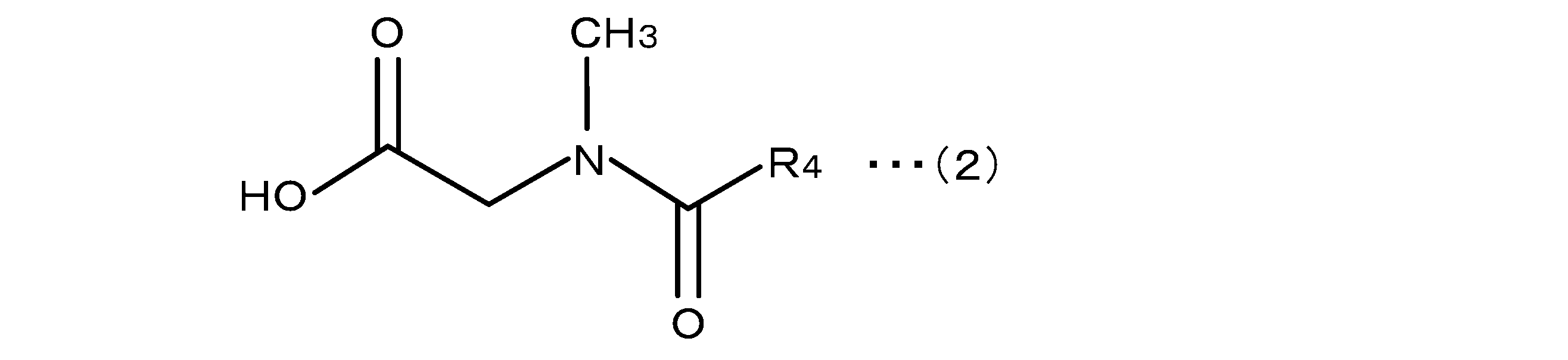
上記式(2)中、R4は、炭素数10以上20以下の鎖状炭化水素基を表す。R4は、炭素数が好ましくは15以上20以下である。また、鎖状炭化水素基は、直鎖炭化水素基でもよく、分岐炭化水素基であってもよい。また、鎖状炭化水素基は、アルキル基、アルケニル基、又は、アルキニル基であってもよい。R4は、好ましくは直鎖炭化水素基であり、より好ましくは直鎖アルケニル基であり、二重結合を有する。
本実施形態に係る導電性ペーストは、第2の分散剤、すなわち上記式(2)で示されるアミノ酸系分散剤を更に含有させることにより、粘度経時変化をより抑えることが可能となる。よって、第1の分散剤と第2の分散剤を含む導電性ペーストは、特に高精細な印刷を要求される電子部品などに好適に用いることができる。
第2の分散剤は、例えば、市販の製品から、上記特性を満たすものを選択して用いることができる。また、第2の分散剤は、従来公知の製造方法を用いて、上記特性を満たすように製造してもよい。
導電性ペースト中、第1の分散剤と、任意に第2の分散剤を含む、分散剤の総含有量は、導電性ペースト100質量%に対して0.4質量%以上2質量%以下であり、0.4質量%以上1.5質量%以下であってもよい。第1の分散剤と第2の分散剤は、主な分散対象が異なると考えられ、分散剤の総含有量が0.4質量%以上2質量%以下の範囲である場合、分散性が向上し、粘度の変化量も低く抑えられる。分散剤の総含有量が0.4質量%未満の場合、分散剤の効果が十分得られない場合がある。分散剤の総含有量が2質量%を超える場合は、過剰な分散剤が乾燥膜表面に残留し、積層時に導電膜表面とグリーンシート表面との密着性を阻害して剥離を生じ、積層体を形成できない場合がある。
すなわち、第1の分散剤の含有量、及び、分散剤の総含有量が上記範囲内である場合、導電性ペーストの粘度を適切な範囲に調整することができ、また、シートアタックやグリーンシートの剥離不良を抑制することができる。
なお、本発明の導電性ペーストは、上記の第1及び第2の分散剤以外の分散剤を、本発明の効果を阻害しない範囲で含んでもよい。上記以外の分散剤としては、例えば、高級脂肪酸、高分子界面活性剤などを含む酸系分散剤、酸系分散剤以外のカチオン系分散剤、ノニオン系分散剤、両性界面活性剤及び高分子系分散剤などを含んでもよい。また、これらの分散剤は、1種または2種以上組み合わせて用いてもよい。
(その他の成分)
本実施形態の導電性ペーストは、必要に応じて、上記の成分以外のその他の成分を含んでもよい。その他の成分としては、例えば、消泡剤、可塑剤、界面活性剤、増粘剤などの従来公知の添加物を用いることができる。
本実施形態の導電性ペーストは、必要に応じて、上記の成分以外のその他の成分を含んでもよい。その他の成分としては、例えば、消泡剤、可塑剤、界面活性剤、増粘剤などの従来公知の添加物を用いることができる。
(導電性ペースト)
本実施形態の導電性ペーストの製造方法は、特に限定されず、従来公知の方法を用いることができる。導電性ペーストは、例えば、上記の各成分を、ボールミル、ビーズミル、3本ロールミル、ミキサーなどで攪拌・混練することにより製造することができる。その際、導電性粉末の表面に予め分散剤を塗布すると、導電性粉末が凝集することなく十分にほぐれて、その表面に分散剤が行きわたるようになり、均一な導電性ペーストを得やすい。また、予め、バインダー樹脂を有機溶剤の一部に溶解させて、有機ビヒクルを作製した後、ペースト調整用の有機溶剤へ、導電性粉末、セラミック粉末、有機ビヒクル及び分散剤を添加した後、攪拌・混練し、導電性ペーストを作製してもよい。
本実施形態の導電性ペーストの製造方法は、特に限定されず、従来公知の方法を用いることができる。導電性ペーストは、例えば、上記の各成分を、ボールミル、ビーズミル、3本ロールミル、ミキサーなどで攪拌・混練することにより製造することができる。その際、導電性粉末の表面に予め分散剤を塗布すると、導電性粉末が凝集することなく十分にほぐれて、その表面に分散剤が行きわたるようになり、均一な導電性ペーストを得やすい。また、予め、バインダー樹脂を有機溶剤の一部に溶解させて、有機ビヒクルを作製した後、ペースト調整用の有機溶剤へ、導電性粉末、セラミック粉末、有機ビヒクル及び分散剤を添加した後、攪拌・混練し、導電性ペーストを作製してもよい。
導電性ペーストは、導電性ペーストの製造24時間経過後の粘度を基準(0%)とした場合、その基準日から110日間静置後の粘度は、±40%以内であるのが好ましい。なお、上記導電性ペーストの粘度は、例えば、実施例に記載した方法(ブルックフィールド社製B型粘度計を用いて10rpm(ずり速度=4sec-1)の条件で測定する方法)等により測定することができる。
導電性ペーストは、積層セラミックコンデンサなどの電子部品に好適に用いることができる。積層セラミックコンデンサは、誘電体グリーンシートを用いて形成される誘電体層及び導電性ペーストを用いて形成される内部電極層を有する。
積層セラミックコンデンサは、誘電体グリーンシートに含まれる誘電体セラミック粉末と導電性ペーストに含まれるセラミック粉末とが同一組成の粉末であることが好ましい。本実施形態の導電性ペーストを用いて製造される積層セラミックコンデンサは、誘電体グリーンシートの厚さが、例えば3μm以下である場合でも、シートアタックやグリーンシートの剥離不良が抑制される。
(電子部品)
以下、本発明の電子部品等の実施形態について、図面を参照しながら説明する。図面においては、適宜、模式的に表現することや、縮尺を変更して表現することがある。また、部材の位置や方向などを、適宜、図1A及び図1Bなどに示すXYZ直交座標系を参照して説明する。このXYZ直交座標系において、X方向およびY方向は水平方向であり、Z方向は鉛直方向(上下方向)である。
以下、本発明の電子部品等の実施形態について、図面を参照しながら説明する。図面においては、適宜、模式的に表現することや、縮尺を変更して表現することがある。また、部材の位置や方向などを、適宜、図1A及び図1Bなどに示すXYZ直交座標系を参照して説明する。このXYZ直交座標系において、X方向およびY方向は水平方向であり、Z方向は鉛直方向(上下方向)である。
図1A及び図1Bは、実施形態に係る電子部品の一例である、積層セラミックコンデンサ1を示す図である。積層セラミックコンデンサ1は、誘電体層12及び内部電極層11を交互に積層した積層体10と外部電極20とを備える。
以下、上記導電性ペーストを使用した積層セラミックコンデンサの製造方法について説明する。まず、グリーンシートからなる誘電体層上に、導電性ペーストを印刷して、乾燥し、乾燥膜を形成する。この乾燥膜を上面に有する複数の誘電体層を、圧着により積層させて積層体(圧着体)を得た後、積層体を焼成して一体化することにより、内部電極層11と誘電体層12とが交互に積層したセラミック積層体10(積層体10)を作製する。その後、セラミック積層体10の両端部に一対の外部電極20を形成することにより積層セラミックコンデンサ1が製造される。以下に、より詳細に説明する。
まず、未焼成のセラミックシートであるグリーンシートを用意する。このグリーンシートとしては、例えば、チタン酸バリウム等の所定のセラミックの原料粉末に、ポリビニルブチラール等の有機バインダーとターピネオール等の溶剤とを加えて得た誘電体層用ペーストを、PETフィルム等の支持フィルム上にシート状に塗布し、乾燥させて溶剤を除去したもの等が挙げられる。なお、グリーンシートからなる誘電体層の厚みは、特に限定されないが、積層セラミックコンデンサの小型化の要請の観点から、0.05μm以上3μm以下が好ましい。
次いで、このグリーンシートの片面に、スクリーン印刷法等の公知の方法によって、上述の導電性ペーストを印刷(塗布)して乾燥し、乾燥膜を形成したものを複数枚、用意する。なお、印刷後の導電性ペースト(乾燥膜)の厚みは、内部電極層11の薄層化の要請の観点から、乾燥後1μm以下とすることが好ましい。
次いで、支持フィルムから、グリーンシートを剥離するとともに、グリーンシートからなる誘電体層とその片面に形成された乾燥膜とが交互に配置されるように積層した後、加熱・加圧処理により積層体を得る。なお、積層体の両面に、導電性ペーストを塗布していない保護用のグリーンシートを更に配置する構成としても良い。
次いで、積層体を所定サイズに切断してグリーンチップを形成した後、当該グリーンチップに対して脱バインダー処理を施し、還元雰囲気下において焼成することにより、セラミック積層体10を製造する。なお、脱バインダー処理における雰囲気は、大気またはN2ガス雰囲気にすることが好ましい。脱バインダー処理を行う際の温度は、例えば200℃以上400℃以下である。また、脱バインダー処理を行う際の、上記温度の保持時間を0.5時間以上24時間以下とすることが好ましい。また、焼成は、内部電極層に用いる金属の酸化を抑制するために還元雰囲気で行われ、また、積層体の焼成を行う際の温度は、例えば、1000℃以上1350℃以下であり、焼成を行う際の、温度の保持時間は、例えば、0.5時間以上8時間以下である。
グリーンチップの焼成を行うことにより、グリーンシート中の有機バインダーが完全に除去されるとともに、セラミックの原料粉末が焼成されて、セラミック製の誘電体層12が形成される。また乾燥膜中の有機ビヒクルが除去されるとともに、ニッケル粉末またはニッケルを主成分とする合金粉末が焼結もしくは溶融、一体化されて、内部電極が形成され、誘電体層12と内部電極層11とが複数枚、交互に積層された積層セラミック焼成体が形成される。なお、酸素を誘電体層の内部に取り込んで信頼性を高めるとともに、内部電極の再酸化を抑制するとの観点から、焼成後の積層セラミック焼成体に対して、アニール処理を施してもよい。
そして、作製した積層セラミック焼成体に対して、一対の外部電極20を設けることにより、積層セラミックコンデンサ1が製造される。例えば、外部電極20は、外部電極層21及びメッキ層22を備える。外部電極層21は、内部電極層11と電気的に接続される。なお、外部電極20の材料としては、例えば、銅やニッケル、またはこれらの合金が好適に使用できる。なお、電子部品は、積層セラミックコンデンサに限定されず、積層セラミックコンデンサ以外の電子部品であってもよい。
以下、本発明を実施例と比較例に基づき詳細に説明するが、本発明は実施例によって何ら限定されるものではない。
[使用材料]
(導電性粉末)
導電性粉末としては、CVD法で作製された市販の平均粒径0.3μmのNi粉末を使用した。
(導電性粉末)
導電性粉末としては、CVD法で作製された市販の平均粒径0.3μmのNi粉末を使用した。
(セラミック粉末)
セラミック粉末としては、市販の平均粒径0.1μmのチタン酸バリウム(BaTiO3)を使用した。
セラミック粉末としては、市販の平均粒径0.1μmのチタン酸バリウム(BaTiO3)を使用した。
(バインダー樹脂)
バインダー樹脂としては、市販のエチルセルロース樹脂(ダウケミカル社製STD-100)を使用した。
バインダー樹脂としては、市販のエチルセルロース樹脂(ダウケミカル社製STD-100)を使用した。
(分散剤)
(1)アミン系分散剤として、下記の分散剤A1~A3を用いた。
分散剤A1:上記一般式(1)中、R1=C12H25、R2=なし、R3=C2H4O、Y=0、Z=1で示され、HLB値が3.8のアミン系分散剤。
分散剤A2:上記一般式(1)中、R1=C12H25、R2=C2H4O、R3=C2H4O、Y=1、Z=1で示され、HLB値が6.4のアミン系分散剤。
分散剤A3:上記一般式(1)中、R1=C12H25、R2=C2H4O、R3=C2H4O、Y=1以上、Z=1以上で示され、HLB値が12.5のポリオキシエチレン基を有するアミン系分散剤(比較例として使用)。
(2)アミノ酸系分散剤として、上記一般式(2)中、R4=C17H33(直鎖炭化水素基)で示される分散剤Bを用いた。
(有機溶剤)
有機溶剤としては、イソボルニルアセテートとエチレングリコールモノブチルエーテルアセテートを混合したものを使用した。
有機溶剤としては、イソボルニルアセテートとエチレングリコールモノブチルエーテルアセテートを混合したものを使用した。
[実施例1]
Ni粉末46質量%、セラミック粉末6.9質量%、ビヒクル中のバインダー樹脂3.2質量%、アミン系分散剤(分散剤A1)を0.6質量%、アミノ酸系分散剤(分散剤B)を0.2質量%、及び、残部として有機溶剤を加え、全体として100質量%となるよう配合し、これらの材料を混合して導電性ペーストを作製した。作製した導電性ペーストの粘度安定性、及び密着性を下記の方法で評価した。評価結果を表1に示す。
Ni粉末46質量%、セラミック粉末6.9質量%、ビヒクル中のバインダー樹脂3.2質量%、アミン系分散剤(分散剤A1)を0.6質量%、アミノ酸系分散剤(分散剤B)を0.2質量%、及び、残部として有機溶剤を加え、全体として100質量%となるよう配合し、これらの材料を混合して導電性ペーストを作製した。作製した導電性ペーストの粘度安定性、及び密着性を下記の方法で評価した。評価結果を表1に示す。
[評価方法]
(粘度安定性:導電性ペーストの粘度の変化量)
導電性ペーストの製造24時間経過後を基準時点とし、その基準時点と、室温(25℃)で基準時点より14日、28日、110日静置後における、それぞれのサンプルの粘度を下記の方法で測定した。そして、製造24時間経過後(基準時点)の粘度を基準(0%)とした場合の、各静置後のサンプルの粘度の変化量を百分率(%)で表した値([(静置後の粘度-製造24時間経過後の粘度)/製造24時間経過後の粘度]×100)を求め、粘度の変化量とした。
(粘度安定性:導電性ペーストの粘度の変化量)
導電性ペーストの製造24時間経過後を基準時点とし、その基準時点と、室温(25℃)で基準時点より14日、28日、110日静置後における、それぞれのサンプルの粘度を下記の方法で測定した。そして、製造24時間経過後(基準時点)の粘度を基準(0%)とした場合の、各静置後のサンプルの粘度の変化量を百分率(%)で表した値([(静置後の粘度-製造24時間経過後の粘度)/製造24時間経過後の粘度]×100)を求め、粘度の変化量とした。
導電性ペーストの粘度は、ブルックフィールド社製B型粘度計を用いて10rpm(ずり速度=4sec-1)の条件で測定した。なお、導電性ペーストの粘度の変化量は少ないほど好ましい。110日静置後の導電性ペーストの粘度の変化量が40%以下である場合を「○」とし、40%を超える場合を「×」として、導電性ペーストの粘度安定性を評価した。
(密着性)
作製した導電性ペーストをグリーンシート上に、スクリーン印刷法にて印刷(塗布)し、乾燥させて、グリーンシート上に乾燥膜を形成したものを複数作製した。これらのシートを5枚積層し、80℃、100kg/cm2の圧力で3分間、熱圧着処理を行い、積層体(圧着体)を形成した。得られた積層体において、密着性を以下の基準で評価した。
作製した導電性ペーストをグリーンシート上に、スクリーン印刷法にて印刷(塗布)し、乾燥させて、グリーンシート上に乾燥膜を形成したものを複数作製した。これらのシートを5枚積層し、80℃、100kg/cm2の圧力で3分間、熱圧着処理を行い、積層体(圧着体)を形成した。得られた積層体において、密着性を以下の基準で評価した。
乾燥膜表面(電極層表面)と、上に積層させたグリーンシート底面との間に1か所でも剥離を生じた場合は、この間の密着性が弱いと判断して「×」とし、剥離を生じなかった場合は、「○」とした。
[実施例2]
アミン系分散剤として、分散剤A2を用いた以外は、実施例1と同様の条件で導電性ペーストを作製した。作製した導電性ペーストの粘度安定性、及び密着性を上記方法で評価した。評価結果を表1に示す。
アミン系分散剤として、分散剤A2を用いた以外は、実施例1と同様の条件で導電性ペーストを作製した。作製した導電性ペーストの粘度安定性、及び密着性を上記方法で評価した。評価結果を表1に示す。
[実施例3]
セラミック粉末の含有量を11.5質量%とした以外は、実施例2と同様の条件で導電性ペーストを作製した。作製した導電性ペーストの粘度安定性、及び密着性を上記方法で評価した。評価結果を表1に示す。
セラミック粉末の含有量を11.5質量%とした以外は、実施例2と同様の条件で導電性ペーストを作製した。作製した導電性ペーストの粘度安定性、及び密着性を上記方法で評価した。評価結果を表1に示す。
[比較例1]
アミン系分散剤として、分散剤A3を用いた以外は、実施例1と同様の条件で導電性ペーストを作製した。作製した導電性ペーストの粘度安定性、及び密着性を上記方法で評価した。評価結果を表1に示す。
アミン系分散剤として、分散剤A3を用いた以外は、実施例1と同様の条件で導電性ペーストを作製した。作製した導電性ペーストの粘度安定性、及び密着性を上記方法で評価した。評価結果を表1に示す。
[実施例4~6、比較例2~4]
アミン系分散剤とアミノ酸系分散剤との含有量を、表2に示した様に変更させた以外は、実施例3と同様の条件で導電性ペーストを作製した。作製した導電性ペーストの粘度の変化量、乾燥膜密度、乾燥膜の表面粗さ、及び密着性を上記方法で評価した。評価結果を表2に示す。
アミン系分散剤とアミノ酸系分散剤との含有量を、表2に示した様に変更させた以外は、実施例3と同様の条件で導電性ペーストを作製した。作製した導電性ペーストの粘度の変化量、乾燥膜密度、乾燥膜の表面粗さ、及び密着性を上記方法で評価した。評価結果を表2に示す。
[評価結果]
実施例の導電性ペーストは、表1および2の結果に示されるように、110日後の粘度変化量が35%以下であり、積層体に剥離も観察されず、良好な粘度安定性や密着性を示した。
実施例の導電性ペーストは、表1および2の結果に示されるように、110日後の粘度変化量が35%以下であり、積層体に剥離も観察されず、良好な粘度安定性や密着性を示した。
これに対し、HLB値が本発明の範囲よりも高い比較例1の導電性ペーストは、粘度安定性に劣り、14日後の粘度変化量が130%と大幅に変化しており、110日後には280%となり、同一の製造条件で導体を形成するのが困難であることが分かる。
また、アミン系分散剤の含有量が本発明の範囲よりも少ない比較例2の導電性ペーストは、構成材料の分散性が低く粘度安定性に劣り、14日後の粘度変化量が36%となり、110日後の粘度変化量が94%と粘度の変化が大きいことが分かる。アミン系分散剤の含有量が本発明の範囲より多い比較例3、及び分散剤の総含有量が本発明の範囲より多い比較例4の導電しペーストは、余剰な分散剤成分が導体表面に残留し、製造された積層体に剥離が生じ、密着性が低下した。
本実施形態に係る導電性ペーストは、分散性に優れるため、経時的な粘度安定性に非常に優れており、かつ積層体において十分な密着性を有しているため、同一ロットでの製造タイミングに差が生じても、同一製造条件でほぼ同じ状態の製品を歩留りよく製造することができる。よって、本実施形態に係る導電性ペーストは、特に携帯電話やデジタル機器などの電子機器に用いられる電子部品である積層セラミックコンデンサの内部電極用の原料として好適に用いることができる。
なお、本発明の技術範囲は、上述の実施形態などで説明した態様に限定されるものではない。上述の実施形態などで説明した要件の1つ以上は、省略されることがある。また、上述の実施形態などで説明した要件は、適宜組み合わせることができる。また、法令で許容される限りにおいて、日本特許出願である特願2018-184104、及び本明細書で引用した全ての文献の内容を援用して本文の記載の一部とする。
1 積層セラミックコンデンサ
10 セラミック積層体
11 内部電極層
12 誘電体層
20 外部電極
21 外部電極層
22 メッキ層
10 セラミック積層体
11 内部電極層
12 誘電体層
20 外部電極
21 外部電極層
22 メッキ層
Claims (12)
- 導電性粉末、セラミック粉末、分散剤、バインダー樹脂、及び有機溶剤を含む導電性ペーストであって、
前記分散剤が3.5以上7.0以下のHLB値を有する第1の分散剤を含有し、
前記第1の分散剤を、導電性ペースト100質量%に対して、0.4質量%以上1質量%以下含有し、
かつ、前記分散剤を、導電性ペースト100質量%に対して、総含有量で0.4質量%以上2質量%以下含有する、
ことを特徴とする導電性ペースト。 - 前記第1の分散剤が、下記一般式(1)で示されるアミン系分散剤であることを特徴とする請求項1に記載の導電性ペースト。

- 前記分散剤が、下記一般式(2)で示されるアミノ酸系分散剤である第2の分散剤を更に含有することを特徴とする請求項1又は請求項2に記載の導電性ペースト。
- 前記導電性粉末が、Ag、Pd、Ni、Cu、Pt、Au、及び、これらの合金の中から選ばれる1種以上の粉末であることを特徴とする請求項1~3のいずれか1項に記載の導電性ペースト。
- 前記導電性粉末を、導電性ペースト100質量%に対して、40質量%以上60質量%以下含有することを特徴とする請求項1~4のいずれか1項に記載の導電性ペースト。
- 前記導電性粉末の平均粒径が、0.01μm以上1.0μm以下であることを特徴とする請求項1~5のいずれか1項に記載の導電性ペースト。
- 前記セラミック粉末が、セラミック粉末100質量%に対して、BaTiO3を80質量%以上含有することを特徴とする請求項1~6のいずれか1項に記載の導電性ペースト。
- 前記セラミック粉末を、導電性ペースト100質量%に対して、2質量%以上30質量%以下含有することを特徴とする請求項1~7のいずれか1項に記載の導電性ペースト。
- 前記セラミック粉末の平均粒径が0.02μm以上0.2μm以下であることを特徴とする請求項1~8のいずれか1項に記載の導電性ペースト。
- 前記バインダー樹脂が、セルロース系樹脂、アクリル系樹脂、及びブチラール系樹脂のうち少なくとも1種を含有することを特徴とする請求項1~9のいずれか1項に記載の導電性ペースト。
- 請求項1~10のいずれか1項に記載の導電性ペーストを用いて形成した導体を有することを特徴とする電子部品。
- 請求項1~10のいずれか1項に記載の導電性ペーストを用いて形成した内部電極層と誘電体層とを積層した積層体を有することを特徴とする積層セラミックコンデンサ。
Priority Applications (2)
| Application Number | Priority Date | Filing Date | Title |
|---|---|---|---|
| KR1020207035840A KR102737839B1 (ko) | 2018-09-28 | 2019-09-26 | 도전성 페이스트, 전자 부품, 및 적층 세라믹 콘덴서 |
| CN201980040510.2A CN112368786B (zh) | 2018-09-28 | 2019-09-26 | 导电性浆料、电子部件以及叠层陶瓷电容器 |
Applications Claiming Priority (2)
| Application Number | Priority Date | Filing Date | Title |
|---|---|---|---|
| JP2018-184104 | 2018-09-28 | ||
| JP2018184104A JP7215047B2 (ja) | 2018-09-28 | 2018-09-28 | 導電性ペースト、電子部品、及び積層セラミックコンデンサ |
Publications (1)
| Publication Number | Publication Date |
|---|---|
| WO2020067362A1 true WO2020067362A1 (ja) | 2020-04-02 |
Family
ID=69950651
Family Applications (1)
| Application Number | Title | Priority Date | Filing Date |
|---|---|---|---|
| PCT/JP2019/038005 Ceased WO2020067362A1 (ja) | 2018-09-28 | 2019-09-26 | 導電性ペースト、電子部品、及び積層セラミックコンデンサ |
Country Status (5)
| Country | Link |
|---|---|
| JP (1) | JP7215047B2 (ja) |
| KR (1) | KR102737839B1 (ja) |
| CN (1) | CN112368786B (ja) |
| TW (1) | TWI813780B (ja) |
| WO (1) | WO2020067362A1 (ja) |
Cited By (1)
| Publication number | Priority date | Publication date | Assignee | Title |
|---|---|---|---|---|
| CN113758833A (zh) * | 2021-09-03 | 2021-12-07 | 天津艾克凯胜石墨烯科技有限公司 | 石墨烯导电浆料粘度测定方法 |
Families Citing this family (5)
| Publication number | Priority date | Publication date | Assignee | Title |
|---|---|---|---|---|
| JP7494554B2 (ja) * | 2020-05-11 | 2024-06-04 | 住友金属鉱山株式会社 | 導電性ペースト、電子部品、及び、積層セラミックコンデンサ |
| JP7552231B2 (ja) * | 2020-10-12 | 2024-09-18 | 住友金属鉱山株式会社 | 導電性ペースト、電子部品、及び、積層セラミックコンデンサ |
| JP7857079B2 (ja) * | 2020-11-26 | 2026-05-12 | 住友金属鉱山株式会社 | 導電性ペースト及び積層セラミックコンデンサ |
| JP7746885B2 (ja) * | 2022-03-07 | 2025-10-01 | 住友金属鉱山株式会社 | 導電性ペースト、電子部品、及び、積層セラミックコンデンサ |
| CN114694898B (zh) * | 2022-06-01 | 2022-10-14 | 西北工业大学 | 一种mlcc镍内电极浆料的制备方法 |
Citations (4)
| Publication number | Priority date | Publication date | Assignee | Title |
|---|---|---|---|---|
| JPH05275861A (ja) * | 1992-03-27 | 1993-10-22 | Kyocera Corp | 多層回路基板 |
| JP2000129318A (ja) * | 1998-10-22 | 2000-05-09 | Dowa Mining Co Ltd | 銀粉およびその製造方法 |
| JP2013149457A (ja) * | 2012-01-19 | 2013-08-01 | Sumitomo Metal Mining Co Ltd | 内部電極用導電ペースト |
| WO2017150438A1 (ja) * | 2016-02-29 | 2017-09-08 | 住友金属鉱山株式会社 | 導電性ペースト、電子部品及び積層セラミックコンデンサ |
Family Cites Families (6)
| Publication number | Priority date | Publication date | Assignee | Title |
|---|---|---|---|---|
| AT12056U1 (de) * | 2010-06-01 | 2011-09-15 | Plansee Se | Kollimator |
| KR101765706B1 (ko) * | 2012-05-18 | 2017-08-07 | 가부시키가이샤 무라타 세이사쿠쇼 | 잉크젯용 잉크, 인쇄방법 및 세라믹 전자부품 |
| JP6292014B2 (ja) | 2014-05-12 | 2018-03-14 | 株式会社村田製作所 | 導電性ペーストおよびセラミック電子部品 |
| KR102410080B1 (ko) * | 2014-07-31 | 2022-06-16 | 스미토모 긴조쿠 고잔 가부시키가이샤 | 도전성 페이스트 |
| JP2018037630A (ja) * | 2016-08-25 | 2018-03-08 | 住友金属鉱山株式会社 | 内部電極用ペーストとその製造方法、及び積層セラミックコンデンサ |
| JP7206671B2 (ja) * | 2018-07-25 | 2023-01-18 | 住友金属鉱山株式会社 | 導電性ペースト、電子部品及び積層セラミックコンデンサ |
-
2018
- 2018-09-28 JP JP2018184104A patent/JP7215047B2/ja active Active
-
2019
- 2019-09-26 KR KR1020207035840A patent/KR102737839B1/ko active Active
- 2019-09-26 CN CN201980040510.2A patent/CN112368786B/zh active Active
- 2019-09-26 WO PCT/JP2019/038005 patent/WO2020067362A1/ja not_active Ceased
- 2019-09-27 TW TW108135293A patent/TWI813780B/zh active
Patent Citations (4)
| Publication number | Priority date | Publication date | Assignee | Title |
|---|---|---|---|---|
| JPH05275861A (ja) * | 1992-03-27 | 1993-10-22 | Kyocera Corp | 多層回路基板 |
| JP2000129318A (ja) * | 1998-10-22 | 2000-05-09 | Dowa Mining Co Ltd | 銀粉およびその製造方法 |
| JP2013149457A (ja) * | 2012-01-19 | 2013-08-01 | Sumitomo Metal Mining Co Ltd | 内部電極用導電ペースト |
| WO2017150438A1 (ja) * | 2016-02-29 | 2017-09-08 | 住友金属鉱山株式会社 | 導電性ペースト、電子部品及び積層セラミックコンデンサ |
Cited By (1)
| Publication number | Priority date | Publication date | Assignee | Title |
|---|---|---|---|---|
| CN113758833A (zh) * | 2021-09-03 | 2021-12-07 | 天津艾克凯胜石墨烯科技有限公司 | 石墨烯导电浆料粘度测定方法 |
Also Published As
| Publication number | Publication date |
|---|---|
| KR20210056951A (ko) | 2021-05-20 |
| CN112368786A (zh) | 2021-02-12 |
| CN112368786B (zh) | 2023-10-03 |
| TW202022893A (zh) | 2020-06-16 |
| KR102737839B1 (ko) | 2024-12-04 |
| JP2020053348A (ja) | 2020-04-02 |
| JP7215047B2 (ja) | 2023-01-31 |
| TWI813780B (zh) | 2023-09-01 |
Similar Documents
| Publication | Publication Date | Title |
|---|---|---|
| JP7750318B2 (ja) | 導電性ペースト、電子部品、及び積層セラミックコンデンサ | |
| CN112106149B (zh) | 导电性浆料、电子部件以及叠层陶瓷电容器 | |
| JP7215047B2 (ja) | 導電性ペースト、電子部品、及び積層セラミックコンデンサ | |
| WO2020137290A1 (ja) | 導電性ペースト、電子部品、及び積層セラミックコンデンサ | |
| WO2021106470A1 (ja) | グラビア印刷用導電性ペースト、電子部品、及び積層セラミックコンデンサ | |
| TWI819190B (zh) | 導電性漿料、電子零件、及積層陶瓷電容器 | |
| JP7206671B2 (ja) | 導電性ペースト、電子部品及び積層セラミックコンデンサ | |
| JP7559489B2 (ja) | 導電性ペースト、電子部品、及び、積層セラミックコンデンサ | |
| JP7586088B2 (ja) | 導電性組成物、導電性ペースト、電子部品、及び積層セラミックコンデンサ | |
| JP2019157089A (ja) | 有機ビヒクルの製造方法、及び、導電性ペーストの製造方法 | |
| JP2021180073A (ja) | 導電性ペースト、電子部品、及び、積層セラミックコンデンサ |
Legal Events
| Date | Code | Title | Description |
|---|---|---|---|
| 121 | Ep: the epo has been informed by wipo that ep was designated in this application |
Ref document number: 19867509 Country of ref document: EP Kind code of ref document: A1 |
|
| ENP | Entry into the national phase |
Ref document number: 20207035840 Country of ref document: KR Kind code of ref document: A |
|
| NENP | Non-entry into the national phase |
Ref country code: DE |
|
| 122 | Ep: pct application non-entry in european phase |
Ref document number: 19867509 Country of ref document: EP Kind code of ref document: A1 |