WO2020054301A1 - 表示装置及びルーム装置 - Google Patents
表示装置及びルーム装置 Download PDFInfo
- Publication number
- WO2020054301A1 WO2020054301A1 PCT/JP2019/031864 JP2019031864W WO2020054301A1 WO 2020054301 A1 WO2020054301 A1 WO 2020054301A1 JP 2019031864 W JP2019031864 W JP 2019031864W WO 2020054301 A1 WO2020054301 A1 WO 2020054301A1
- Authority
- WO
- WIPO (PCT)
- Prior art keywords
- substrate
- light
- state
- display
- display device
- Prior art date
- Legal status (The legal status is an assumption and is not a legal conclusion. Google has not performed a legal analysis and makes no representation as to the accuracy of the status listed.)
- Ceased
Links
Images





Classifications
-
- G—PHYSICS
- G02—OPTICS
- G02F—OPTICAL DEVICES OR ARRANGEMENTS FOR THE CONTROL OF LIGHT BY MODIFICATION OF THE OPTICAL PROPERTIES OF THE MEDIA OF THE ELEMENTS INVOLVED THEREIN; NON-LINEAR OPTICS; FREQUENCY-CHANGING OF LIGHT; OPTICAL LOGIC ELEMENTS; OPTICAL ANALOGUE/DIGITAL CONVERTERS
- G02F1/00—Devices or arrangements for the control of the intensity, colour, phase, polarisation or direction of light arriving from an independent light source, e.g. switching, gating or modulating; Non-linear optics
- G02F1/01—Devices or arrangements for the control of the intensity, colour, phase, polarisation or direction of light arriving from an independent light source, e.g. switching, gating or modulating; Non-linear optics for the control of the intensity, phase, polarisation or colour
- G02F1/13—Devices or arrangements for the control of the intensity, colour, phase, polarisation or direction of light arriving from an independent light source, e.g. switching, gating or modulating; Non-linear optics for the control of the intensity, phase, polarisation or colour based on liquid crystals, e.g. single liquid crystal display cells
- G02F1/137—Devices or arrangements for the control of the intensity, colour, phase, polarisation or direction of light arriving from an independent light source, e.g. switching, gating or modulating; Non-linear optics for the control of the intensity, phase, polarisation or colour based on liquid crystals, e.g. single liquid crystal display cells characterised by the electro-optical or magneto-optical effect, e.g. field-induced phase transition, orientation effect, guest-host interaction or dynamic scattering
-
- B—PERFORMING OPERATIONS; TRANSPORTING
- B60—VEHICLES IN GENERAL
- B60R—VEHICLES, VEHICLE FITTINGS, OR VEHICLE PARTS, NOT OTHERWISE PROVIDED FOR
- B60R1/00—Optical viewing arrangements; Real-time viewing arrangements for drivers or passengers using optical image capturing systems, e.g. cameras or video systems specially adapted for use in or on vehicles
- B60R1/12—Mirror assemblies combined with other articles, e.g. clocks
-
- G—PHYSICS
- G02—OPTICS
- G02F—OPTICAL DEVICES OR ARRANGEMENTS FOR THE CONTROL OF LIGHT BY MODIFICATION OF THE OPTICAL PROPERTIES OF THE MEDIA OF THE ELEMENTS INVOLVED THEREIN; NON-LINEAR OPTICS; FREQUENCY-CHANGING OF LIGHT; OPTICAL LOGIC ELEMENTS; OPTICAL ANALOGUE/DIGITAL CONVERTERS
- G02F1/00—Devices or arrangements for the control of the intensity, colour, phase, polarisation or direction of light arriving from an independent light source, e.g. switching, gating or modulating; Non-linear optics
- G02F1/01—Devices or arrangements for the control of the intensity, colour, phase, polarisation or direction of light arriving from an independent light source, e.g. switching, gating or modulating; Non-linear optics for the control of the intensity, phase, polarisation or colour
- G02F1/13—Devices or arrangements for the control of the intensity, colour, phase, polarisation or direction of light arriving from an independent light source, e.g. switching, gating or modulating; Non-linear optics for the control of the intensity, phase, polarisation or colour based on liquid crystals, e.g. single liquid crystal display cells
- G02F1/133—Constructional arrangements; Operation of liquid crystal cells; Circuit arrangements
- G02F1/1333—Constructional arrangements; Manufacturing methods
- G02F1/1335—Structural association of cells with optical devices, e.g. polarisers or reflectors
- G02F1/133528—Polarisers
- G02F1/133536—Reflective polarizers
-
- G—PHYSICS
- G02—OPTICS
- G02F—OPTICAL DEVICES OR ARRANGEMENTS FOR THE CONTROL OF LIGHT BY MODIFICATION OF THE OPTICAL PROPERTIES OF THE MEDIA OF THE ELEMENTS INVOLVED THEREIN; NON-LINEAR OPTICS; FREQUENCY-CHANGING OF LIGHT; OPTICAL LOGIC ELEMENTS; OPTICAL ANALOGUE/DIGITAL CONVERTERS
- G02F1/00—Devices or arrangements for the control of the intensity, colour, phase, polarisation or direction of light arriving from an independent light source, e.g. switching, gating or modulating; Non-linear optics
- G02F1/01—Devices or arrangements for the control of the intensity, colour, phase, polarisation or direction of light arriving from an independent light source, e.g. switching, gating or modulating; Non-linear optics for the control of the intensity, phase, polarisation or colour
- G02F1/13—Devices or arrangements for the control of the intensity, colour, phase, polarisation or direction of light arriving from an independent light source, e.g. switching, gating or modulating; Non-linear optics for the control of the intensity, phase, polarisation or colour based on liquid crystals, e.g. single liquid crystal display cells
- G02F1/133—Constructional arrangements; Operation of liquid crystal cells; Circuit arrangements
- G02F1/1333—Constructional arrangements; Manufacturing methods
- G02F1/1343—Electrodes
- G02F1/13439—Electrodes characterised by their electrical, optical, physical properties; materials therefor; method of making
-
- G—PHYSICS
- G02—OPTICS
- G02F—OPTICAL DEVICES OR ARRANGEMENTS FOR THE CONTROL OF LIGHT BY MODIFICATION OF THE OPTICAL PROPERTIES OF THE MEDIA OF THE ELEMENTS INVOLVED THEREIN; NON-LINEAR OPTICS; FREQUENCY-CHANGING OF LIGHT; OPTICAL LOGIC ELEMENTS; OPTICAL ANALOGUE/DIGITAL CONVERTERS
- G02F1/00—Devices or arrangements for the control of the intensity, colour, phase, polarisation or direction of light arriving from an independent light source, e.g. switching, gating or modulating; Non-linear optics
- G02F1/01—Devices or arrangements for the control of the intensity, colour, phase, polarisation or direction of light arriving from an independent light source, e.g. switching, gating or modulating; Non-linear optics for the control of the intensity, phase, polarisation or colour
- G02F1/13—Devices or arrangements for the control of the intensity, colour, phase, polarisation or direction of light arriving from an independent light source, e.g. switching, gating or modulating; Non-linear optics for the control of the intensity, phase, polarisation or colour based on liquid crystals, e.g. single liquid crystal display cells
- G02F1/133—Constructional arrangements; Operation of liquid crystal cells; Circuit arrangements
- G02F1/1333—Constructional arrangements; Manufacturing methods
- G02F1/1347—Arrangement of liquid crystal layers or cells in which the final condition of one light beam is achieved by the addition of the effects of two or more layers or cells
- G02F1/13471—Arrangement of liquid crystal layers or cells in which the final condition of one light beam is achieved by the addition of the effects of two or more layers or cells in which all the liquid crystal cells or layers remain transparent, e.g. FLC, ECB, DAP, HAN, TN, STN, SBE-LC cells
-
- G—PHYSICS
- G09—EDUCATION; CRYPTOGRAPHY; DISPLAY; ADVERTISING; SEALS
- G09F—DISPLAYING; ADVERTISING; SIGNS; LABELS OR NAME-PLATES; SEALS
- G09F9/00—Indicating arrangements for variable information in which the information is built-up on a support by selection or combination of individual elements
-
- B—PERFORMING OPERATIONS; TRANSPORTING
- B60—VEHICLES IN GENERAL
- B60R—VEHICLES, VEHICLE FITTINGS, OR VEHICLE PARTS, NOT OTHERWISE PROVIDED FOR
- B60R1/00—Optical viewing arrangements; Real-time viewing arrangements for drivers or passengers using optical image capturing systems, e.g. cameras or video systems specially adapted for use in or on vehicles
- B60R1/12—Mirror assemblies combined with other articles, e.g. clocks
- B60R2001/1215—Mirror assemblies combined with other articles, e.g. clocks with information displays
-
- B—PERFORMING OPERATIONS; TRANSPORTING
- B60—VEHICLES IN GENERAL
- B60R—VEHICLES, VEHICLE FITTINGS, OR VEHICLE PARTS, NOT OTHERWISE PROVIDED FOR
- B60R1/00—Optical viewing arrangements; Real-time viewing arrangements for drivers or passengers using optical image capturing systems, e.g. cameras or video systems specially adapted for use in or on vehicles
- B60R1/12—Mirror assemblies combined with other articles, e.g. clocks
- B60R2001/1253—Mirror assemblies combined with other articles, e.g. clocks with cameras, video cameras or video screens
-
- B—PERFORMING OPERATIONS; TRANSPORTING
- B60—VEHICLES IN GENERAL
- B60R—VEHICLES, VEHICLE FITTINGS, OR VEHICLE PARTS, NOT OTHERWISE PROVIDED FOR
- B60R2300/00—Details of viewing arrangements using cameras and displays, specially adapted for use in a vehicle
- B60R2300/20—Details of viewing arrangements using cameras and displays, specially adapted for use in a vehicle characterised by the type of display used
-
- B—PERFORMING OPERATIONS; TRANSPORTING
- B60—VEHICLES IN GENERAL
- B60R—VEHICLES, VEHICLE FITTINGS, OR VEHICLE PARTS, NOT OTHERWISE PROVIDED FOR
- B60R2300/00—Details of viewing arrangements using cameras and displays, specially adapted for use in a vehicle
- B60R2300/80—Details of viewing arrangements using cameras and displays, specially adapted for use in a vehicle characterised by the intended use of the viewing arrangement
- B60R2300/802—Details of viewing arrangements using cameras and displays, specially adapted for use in a vehicle characterised by the intended use of the viewing arrangement for monitoring and displaying vehicle exterior blind spot views
-
- H—ELECTRICITY
- H01—ELECTRIC ELEMENTS
- H01C—RESISTORS
- H01C13/00—Resistors not provided for elsewhere
Definitions
- the present disclosure relates to a display device and a room device capable of displaying an image in a reflection state in which incident light is reflected and in a transmission state in which incident light is transmitted.
- Patent Document 1 describes a device that can be switched between a display state for displaying an image and a mirror state (reflection state) where a reflected image is obtained.
- the quality of the display state or the quality of the mirror state may be affected by the charging between the electrodes.
- the present disclosure has an object to provide a display device and a room device that can be switched between a display state in which an image is displayed and a mirror state in which a reflected image is obtained, and that can suppress charging between electrodes.
- the display device includes a display panel, a front panel that overlaps with the display panel, and switches between a reflection state in which incident light is reflected and a transmission state in which incident light is transmitted,
- the panel includes a first substrate, a second substrate facing the first substrate, a liquid crystal layer sealed between the first substrate and the second substrate, and a liquid crystal layer of the first substrate.
- a first light-transmitting electrode provided on one side, a second light-transmitting electrode provided on the side of the second substrate on which the liquid crystal layer is provided, and an electrical connection to the second light-transmitting electrode
- a discharge resistor provided on the second substrate; and a first conductive column electrically connecting the first light-transmissive electrode and the discharge resistor.
- a room device is a room device capable of displaying an image in a reflection state in which incident light is reflected and in a transmission state in which incident light is transmitted, wherein the display device and the image behind the vehicle are displayed.
- An image pickup device for picking up an image, wherein the image is displayed on the display panel when the applied voltage is equal to or higher than a threshold value.
- FIG. 1 is a perspective view illustrating an example of the configuration of the display device of the present embodiment.
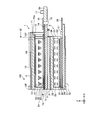
- FIG. 2 is a sectional view of the display device of the present embodiment.
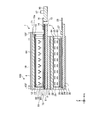
- FIG. 3 is a sectional view of the display device of the present embodiment.
- FIG. 4 is a sectional view of the display device of the present embodiment.
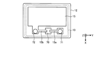
- FIG. 5 is a plan view for explaining the arrangement of the discharge resistors and the conductive columns on the second substrate of the present embodiment.
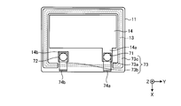
- FIG. 6 is a plan view for explaining the arrangement of the conductive columns on the first substrate of the present embodiment.
- FIG. 7 is an explanatory diagram schematically comparing and explaining the size of the pixel of the display panel and the size of the drive electrode.
- FIG. 8 is a block diagram for explaining the display device of the present embodiment.
- FIG. 8 is a block diagram for explaining the display device of the present embodiment.
- FIG. 9 is a schematic diagram for explaining a display state in which an image can be displayed in a transmission state in which incident light is transmitted.
- FIG. 10 is a schematic diagram for explaining a reflection state in which incident light is reflected.
- FIG. 11 is an explanatory diagram for schematically explaining the relationship between the transmission axis of the first polarizing member and the transmission axis of the optical sheet.
- FIG. 12 is a diagram illustrating an attached state of the room device.
- FIG. 1 is a perspective view showing an example of the configuration of the display device of the present embodiment.
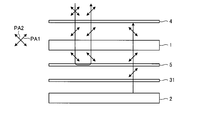
- the display device 100 includes a first polarizing member 4, a front panel 1, an optical sheet 5, a second polarizing member 31, a display panel 2, a third polarizing member 32, and a backlight 3.
- one direction of the plane of the display panel 2 is defined as an X direction
- a direction orthogonal to the X direction on the plane of the display panel 2 is defined as a Y direction
- a direction orthogonal to the XY plane is defined as a Z direction. I have.
- the side having the display surface (or upper surface) on which the display panel 2 displays an image in the Z direction is referred to as the display surface side (or the upper surface side), and the back surface (or the upper surface) opposite to the display surface (or the upper surface) in the Z direction.
- the side having the lower surface is referred to as a rear surface (or a lower surface).
- the third polarizing member 32 and the backlight 3 overlap the display panel 2 on the back side of the display panel 2 when viewed in the Z direction.
- the backlight 3 is an illumination device that emits light toward the display panel 2.
- the backlight 3 has, for example, a light source and a light guide plate, and emits light from an emission surface facing the display panel 2 while scattering light emitted from the light source with the light guide plate.
- the backlight 3 may have a prism sheet or a diffusion sheet between the light guide plate and the third polarizing member 32.
- the first polarizing member 4 On the display surface side of the display panel 2 in the Z direction, the first polarizing member 4, the front panel 1, the optical sheet 5, and the second polarizing member 31 overlap the display panel 2 in this order. As described above, the front panel 1 overlaps the display panel 2.
- FIG. 2 is a cross-sectional view of the display device of the present embodiment.
- FIG. 2 is a diagram illustrating the display device 100 in a display state where an image is displayed.
- FIG. 3 is a sectional view of the display device of the present embodiment.
- FIG. 4 is a sectional view of the display device of the present embodiment.
- FIG. 3 is a diagram illustrating the display device 100 in a reflection state in which incident light is reflected.
- 2 and 3 are schematic cross sections taken along the line II-II shown in FIG.
- FIG. 4 is a schematic cross section taken along the line IV-IV shown in FIG.
- FIG. 5 is a plan view for explaining the arrangement of the discharge resistors and the conductive columns on the second substrate of the present embodiment.
- FIG. 6 is a plan view for explaining the arrangement of the conductive columns on the first substrate of the present embodiment.
- FIG. 7 is an explanatory diagram schematically comparing and explaining the size of the pixel of the display panel and the size of the drive electrode.
- the display panel 2 is a so-called liquid crystal display device.
- the display panel 2 includes a light-transmitting substrate 21, a light-transmitting substrate 22, and a liquid crystal layer 29 sealed between the substrate 21 and the substrate 22 with a sealing layer 23.
- the display panel 2 is not limited to a liquid crystal display device, but may be a display device of an EL (Electro-Luminescence) type or the like.
- the liquid crystal layer 29 modulates light passing through the liquid crystal layer 29 according to the state of an electric field.
- a horizontal electric field mode such as FFS (fringe field switching), which is a form of IPS (in-plane switching)
- FFS far field switching
- IPS in-plane switching
- An electric field mode may be used.
- liquid crystal of various modes such as TN (Twisted Nematic: Twisted Nematic), VA (Virtual Alignment: vertical alignment), and ECB (Electrically Controlled Birefringence: electric field control birefringence) may be used.
- FIG. 7 is an explanatory diagram for schematically comparing and explaining the size of the pixel of the display panel and the size of the drive electrode.
- the display panel 2 displays an image. As shown in FIG. 7, the display panel 2 has a large number of pixels Pix arranged in a two-dimensional array. The light emitted from the backlight 3 (see FIG. 1) enters the display panel 2. The display panel 2 displays an image by changing the transmittance of light incident on each pixel Pix.
- the display device 100 of the present embodiment can be applied to both a display device for monochrome display and a display device for color display.
- one pixel Pix (unit pixel) serving as a unit for forming a color image includes a plurality of sub-pixels (sub-pixels). More specifically, in a display device that supports color display, one pixel is, for example, a sub-pixel that displays red (Red; R), a sub-pixel that displays green (Green; G), and a sub-pixel that displays blue (Blue; B). ) Is displayed.
- One pixel is not limited to a combination of RGB three primary color sub-pixels, and one pixel may be formed by adding one or more color sub-pixels to the RGB three primary color sub-pixels. . More specifically, for example, one pixel is configured by adding a sub-pixel for displaying white (White) for improving luminance, or at least one for displaying a complementary color in order to expand a color reproduction range. It is also possible to form one pixel by adding sub-pixels.
- the pixel electrode 25 and the common electrode 24 are insulated by the insulating layer 26 and face each other in the Z direction perpendicular to the surface of the substrate 21.
- the pixel electrode 25 and the common electrode 24 are light-transmitting electrodes formed of a light-transmitting conductive material (light-transmitting conductive oxide) such as ITO (Indium Tin Oxide).
- the substrate 21 is a translucent substrate such as glass or resin.
- an alignment film 83 is provided on the liquid crystal layer 29 side of the substrate 21, an alignment film 83 is provided.
- a third polarizing member 32 is disposed.
- a color filter (not shown) and an alignment film 84 are provided on the liquid crystal layer 29 side of the substrate 22 shown in FIGS. 2 and 3.
- the color filter includes, for example, a color region colored in three colors of red (R), green (G), and blue (B).
- a second polarizing member 31 is disposed on the side of the substrate 22 opposite to the liquid crystal layer 29 .
- the display panel 2 includes a drive circuit 27 called a driver IC.
- the flexible printed circuit board (FPC (Flexible Printed Circuits)) 27 transmits a signal to the drive circuit 27 and a drive power for driving the drive circuit 27.
- FPC Flexible Printed Circuits
- the front panel 1 includes a first substrate 11, a second substrate 12, and a liquid crystal sealed with a sealing layer 13 between the first substrate 11 and the second substrate 12. And a layer 19.
- the first substrate 11 and the second substrate 12 are translucent substrates such as glass and resin.
- the liquid crystal layer 19 changes the polarization direction of incident light passing through the liquid crystal layer 19 according to the state of an electric field.
- a TN mode is used for the liquid crystal layer 19.
- the first light-transmitting electrode 14 and the second light-transmitting electrode 15 face each other in the Z direction perpendicular to the surface of the first substrate 11.
- the first light-transmitting electrode 14 and the second light-transmitting electrode 15 are formed of a light-transmitting conductive material (light-transmitting conductive oxide) such as ITO.
- connection wirings 15a and 15b are in the same layer as the second light-transmitting electrode 15, and a light-transmitting conductive material (a light-transmitting conductive oxide) such as ITO, which is the same material as the second light-transmitting electrode 15. Is formed.
- a light-transmitting conductive material a light-transmitting conductive oxide
- ITO a light-transmitting conductive oxide
- connection wirings 14a and 14b are formed simultaneously with the first light-transmitting electrode 14. Therefore, the connection wirings 14a and 14b are in the same layer as the first light-transmitting electrode 14, and a light-transmitting conductive material (light-transmitting conductive oxide) such as ITO, which is the same material as the first light-transmitting electrode 14. Is formed. As shown in FIG. 5, the first translucent electrode 14 and the connection wiring 14a are integrally formed and are electrically connected.
- the first translucent electrode 14 is covered with an insulating film 85 of silicon nitride. On the insulating film 85, the above-described alignment film 81 is laminated.
- the first light-transmissive electrode 14 is a drive electrode whose supplied voltage changes and changes the state of the liquid crystal layer 19 by an electric field.
- the second translucent electrode 15 is a fixed potential electrode that maintains a fixed potential with a fixed voltage.
- front panel 1 has first conductive pillars (first conductive members) 71, which are members that electrically connect between first substrate 11 and second substrate 12. , A second conductive column (second conductive member) 72.
- the first conductive pillar 71 and the second conductive pillar 72 are formed by conductive spacers.
- the second conductive pillar 72 is electrically connected to the second translucent electrode 15.
- the conductive spacers forming the first conductive columns 71 and the second conductive columns 72 are formed by plating the spacers with a conductive material.
- the discharge resistor 70 is formed of, for example, a metal oxide film such as chromium oxide or ITO or a resin film.
- the resistance value of the discharge resistor 70 is 10 k ⁇ or more and 100 M ⁇ or less. Since the chromium oxide can be made black, the alignment marker may be formed of chromium oxide at the same layer as the discharge resistor 70 and at a different position from the discharge resistor 70. Thereby, the step of forming the alignment marker can be omitted.
- connection wiring 15a connects the discharge resistor 70 and the first conductive pillar 71.
- connection wiring 15 b connects the discharge resistor 70 to the second translucent electrode 15 and the second conductive column 72.
- front panel 1 has a conductive metal layer 73 such as aluminum. As shown in FIG. 6, the metal layer 73 is patterned and has metal layers 73a, 17b, and 17c.
- the flexible printed circuit (FPC) 18 is electrically connected to the front panel 1 and the bonding pads 74.
- the bonding pad 74 has a plurality of bonding pad terminals 74a, 74b.
- the metal layer 73a electrically connects the connection wiring 14a and the bonding pad terminal 74a. Since the first light-transmitting electrode 14 and the connection wiring 14a are electrically connected, the metal layer 73a serves as a wiring for electrically connecting the first light-transmitting electrode 14 and the bonding pad terminal 74a. .
- the metal layer 73b electrically connects the connection wiring 14b and the bonding pad terminal 74b. As shown in FIG. 4, a second conductive column 72 is formed on connection wiring 14b.
- the metal layer 73b serves as a wiring for connecting the second conductive pillar 72 electrically connected to the second translucent electrode 15 and the bonding pad terminal 74b.
- the second conductive pillar 72 may be formed on the metal layer 73b without the connection wiring 14b.
- the metal layer 73c is arranged along the frame region 10F.
- the metal layer 73c shields the frame region 10F from light so that the light transmittance of the frame region 10F is lower than the light transmittance of the active region 10.
- the bonding pad 74 may be formed of the same light-transmitting conductive material as the first light-transmitting electrode 14.
- the first translucent electrode 14 and the flexible printed board 18 may be connected by an anisotropic conductive film (ACF).
- ACF anisotropic conductive film
- the front panel 1 is connected to a drive circuit 17 mounted on a printed board 99 via a flexible printed board (FPC) 18.
- the drive circuit 17 transmits the power of the first light-transmitting electrode 14 and the second light-transmitting electrode 15 to the front panel via the FPC 18.
- a base layer 64 of cycloolefin polymer On the side of the second substrate 12 opposite to the liquid crystal layer 19, there is a base layer 64 of cycloolefin polymer. A rubbing process is performed on the display surface side of the base material layer 64 to give a specific orientation.
- the first polarizing member 4 is formed on the display surface side of the base material layer 64. In other words, the first polarizing member 4 is on the surface of the second substrate 12 opposite to the liquid crystal layer 19.
- the first polarizing member 4 is a coating type polarizing layer in which a liquid crystal material and a dichroic dye are mixed. When the liquid crystal material self-aligns along the specific alignment given to the base material layer 64, the dichroic dye is also aligned in one direction, and the first polarizing member 4 is rotated in the second direction orthogonal to the first polarizing direction. Absorbs linearly polarized light in the polarization direction.
- optical sheet 5 linearly polarized light in the first polarization direction is transmitted, and linearly polarized light in the second polarization direction is reflected.
- the optical sheet 5 is also called a reflective polarizing plate.
- the front panel 1 has an active area 10 through which incident light or light from the display panel 2 passes, and a frame area 10F around the active area 10. As shown in FIG. 7, the area of the active area 10 is the same as the display area in which all the pixels Pix are arranged.
- FIG. 8 is a block diagram for explaining the display device of the present embodiment.
- the display device 100 of the present embodiment is used as a vehicle interior mirror.
- the control unit 9 is, for example, a computer including a CPU (Central Processing Unit) as an arithmetic device and a memory as a storage device.
- the control unit 9 can also realize various functions by executing a computer program using these hardware resources.
- control unit 9 reads out a computer program stored in a predetermined storage unit (not shown), expands the computer program in a memory, and causes the CPU to execute an instruction included in the program expanded in the memory.
- control unit 9 includes a mirror state determination unit 93 and an image control unit 94.
- the mirror state determination unit 93 and the image control unit 94 are functions of the control unit 9 that are each realized by executing a computer program using hardware resources.
- the image control unit 94 controls the turning on and off of the backlight 3 and the light intensity and the light intensity at the time of turning on, according to the execution result of the instruction by the CPU. Further, the image control unit 94 transmits an image signal to be displayed on the display panel 2 to the drive circuit 27 via the flexible printed circuit board 28 in accordance with the execution result of the instruction by the CPU, and the drive circuit 27 transmits the image signal to the display panel 2. Display the image.
- the mirror state determination unit 93 controls the drive circuit 17 according to the display state command signal of the input unit 202, and the drive circuit 17 applies a voltage to the first translucent electrode 14 via the FPC 18. To As a result, the voltage of the first translucent electrode 14 becomes higher than the threshold.
- the mirror surface state determination unit 93 controls the drive circuit 17 according to the reflection state command signal of the input unit 202, and the drive circuit 17 does not apply a voltage to the first translucent electrode 14 via the FPC 18. To As a result, the voltage applied to the first translucent electrode 14 becomes lower than the threshold.
- the control unit 9 is connected to the imaging device 201 of the vehicle 200.
- the imaging device 201 captures an image of the rear BD of the vehicle 200, and an image of the rear BD of the vehicle 200 is transmitted to the control unit 9.
- the display device 100 displays an image of the BD behind the vehicle 200.
- the position where the imaging device 201 is attached to the vehicle may be a position where the FD ahead of the vehicle 200 can be photographed, or a position where at least one of the periphery of the vehicle 200 and the inside of the vehicle 200 can be photographed.
- FIG. 9 is a schematic diagram for explaining a display state in which an image can be displayed in a transmission state in which incident light is transmitted.
- the first polarizing member 4 absorbs linearly polarized light having a second polarization direction PA2 orthogonal to the first polarization direction PA1.
- the linearly polarized light in the first polarization direction PA1 passes through the first polarization member 4 and enters the front panel 1.
- the drive circuit 17 is in a state of applying a voltage to the first translucent electrode 14.
- the linearly polarized light in the first polarization direction PA1 incident from the first polarization member 4 is emitted to the optical sheet 5 as the linearly polarized light in the first polarization direction PA1.
- the first polarizing member 4 when the display panel 2 displays an image, the first polarizing member 4, the front panel 1, and the optical sheet 5 are in a state where the shutter is opened for linearly polarized light in the first polarization direction PA1, and the image is easily visible. I do.
- the linearly polarized light having the first polarization direction PA1 incident from the front panel 1 is transmitted.
- the second polarizing member 31 transmits linearly polarized light in the first polarization direction PA1.
- the image on the display panel 2 is visible from the display surface side of the first polarizing member 4.
- the display panel 2 emits an image through the second polarizing member 31 with linearly polarized light in the first polarization direction PA1.
- the linearly polarized light having the first polarization direction PA1 incident from the display panel 2 is transmitted.
- the drive circuit 17 operates so that the transmission state is such that incident light is transmitted.
- the image control unit 94 controls the backlight 3 and the display panel 2, and displays an image on the display panel 2.
- FIG. 10 is a schematic diagram for explaining a reflection state in which incident light is reflected.
- the first polarizing member 4 absorbs linearly polarized light having a second polarization direction PA2 orthogonal to the first polarization direction PA1.
- the linearly polarized light in the first polarization direction PA1 passes through the first polarization member 4 and enters the front panel 1.
- the drive circuit 17 is in a state where no voltage is applied to the first light-transmitting electrode 14.
- the linearly polarized light having the first polarization direction PA1 incident from the first polarizing member 4 is converted into linearly polarized light having the second polarization direction PA2, and is emitted to the optical sheet 5.
- the linearly polarized light having the second polarization direction PA2 incident from the front panel 1 is reflected.
- Linear polarized light in the first polarization direction PA1 from the front panel 1 is transmitted through the first polarizing member 4, and when viewed from the display surface side of the first polarizing member 4, the image on the display surface side of the first polarizing member 4 is a mirror surface. Is displayed as follows.
- the first polarization member 4 the front panel 1, and the optical sheet 5 are converted into the second polarization obtained by converting the linear polarization in the first polarization direction PA1 emitted from the display panel 2.
- the shutter is closed for the linearly polarized light in the direction PA2, making it difficult to view the image.
- the display panel 2 emits an image through the second polarizing member 31 using linearly polarized light in the first polarization direction PA1.
- the linearly polarized light having the first polarization direction PA1 incident from the display panel 2 is transmitted.
- the linearly polarized light having the first polarization direction PA ⁇ b> 1 incident from the optical sheet 5 is converted into linearly polarized light having the second polarization direction PA ⁇ b> 2 and emitted to the first polarizing member 4.
- the drive circuit 17 operates so that the incident light is reflected. In the reflection state, even if an image is displayed on the display panel 2, it is difficult to visually recognize the image. Therefore, when the mirror state determination unit 93 shown in FIG. 8 receives the command signal of the reflection state of the input unit 202, the image control unit 94 An image is not displayed on the display panel 2.
- the first polarizing member 4 does not contain iodine. Iodine has the property of absorbing the shorter wavelength side of visible light. Instead of the first polarizing member 4, a general iodine is adsorbed on a PVA (Polyvinyl Alcohol) film, and the polarizing plate is stretched in one direction to align molecules in a certain direction. In the case of a mirror state (reflection state) where an image can be obtained, the wavelength on the short wavelength side of the reflection image is absorbed by iodine, the whiteness becomes greenish, and the color of the reflection image may be shifted. On the other hand, in the display device 100 of the present embodiment, the wavelength on the short wavelength side of the reflected image is less likely to be absorbed by the first polarizing member 4 than iodine, and the whiteness is close to neutral.
- PVA Polyvinyl Alcohol
- the first polarizing member 4 instead of using the above-mentioned coating type polarizing plate as the first polarizing member 4, a general polarizing plate which adsorbs iodine on a PVA film and stretches in one direction to align molecules in a certain direction is used.
- the smoothness of the surface is poor due to stretching of the polarizing plate, and the reflection image may be uneven.
- the display device 100 of the present embodiment uses the first polarizing member 4 that is not stretched. For this reason, since the surface of the first polarizing member 4 has smoothness, unevenness of the reflected image is suppressed.
- the material of the first polarizing member 4 can be selected according to the required degree of polarization and unevenness of the reflected image. It is also possible to make the material of the polarizing plate different for each region.
- the display device 100 includes the first polarizing member 4, the optical sheet 5, the front panel 1, the second polarizing member 31, and the display panel 2.
- the first polarizing member 4 absorbs linearly polarized light having a second polarization direction PA2 orthogonal to the first polarization direction PA1.
- the optical sheet 5 reflects linearly polarized light in the second polarization direction PA2 and transmits linearly polarized light in the first polarization direction PA1.
- the front panel 1 can change the polarization direction of the incident light to another polarization direction according to the applied voltage.
- the front panel 1 is disposed between the first polarizing member 4 and the optical sheet 5.
- the display panel 2 is overlapped with the front panel 1 in the Z direction with respect to the optical sheet 5 via a second polarizing member 31 that transmits linearly polarized light in the second polarization direction PA2.
- the display device 100 can be switched between a display state in which the images shown in FIGS. 3 and 9 are displayed and a mirror state (reflection state) in which the reflection images shown in FIGS. 2 and 10 are obtained.
- the front panel 1 is closer to the viewer than the display panel 2.
- the front panel 1 has a first front panel state in which the incident linearly polarized light in the first polarization direction PA1 is emitted as linearly polarized light in the first polarization direction PA1, and the front panel 1 converts the incident linearly polarized light in the first polarization direction PA1 into the second polarization direction.
- This is a panel that can be switched to either a second front panel state in which the light is converted into linearly polarized light of PA2 and emitted, in accordance with a state in which the drive circuit 17 applies a voltage to the first translucent electrode 14.
- a reflection state is established, and in the second front panel state, a display state is established.
- the power consumption in the reflection state is lower than the power consumption in the display state.
- the display device 100 reflects the incident light.
- power consumption can be reduced in the reflection state.
- FIG. 11 is an explanatory diagram for schematically explaining the relationship between the transmission axis of the first polarizing member and the transmission axis of the optical sheet.
- FIG. 11 shows the transmission axis direction PU1 of the first polarizing member 4, the rubbing direction PB2 of the alignment film 82, the rubbing direction PB1 of the alignment film 81, the transmission axis direction PU2 of the optical sheet 5, and the reflection of the optical sheet 5.
- the axial direction PM is shown.
- the rubbing direction PB2 of the alignment film 82 and the rubbing direction PB1 of the alignment film 81 are directions that intersect in a plan view.
- the transmission axis direction PU1 of the first polarizing member 4 and the transmission axis direction PU2 of the optical sheet 5 are parallel.
- the transmission axis direction PU1 of the first polarizing member 4 and the reflection axis direction PM of the optical sheet 5 are intersecting directions.
- the first polarizing member 4 and the optical sheet 5 transmit linearly polarized light in the first polarization direction PA1.
- the front panel 1 since the front panel 1 has the insulating film 85, short-circuiting between the first light-transmitting electrode 14 and the second light-transmitting electrode 15 is difficult even if there is a foreign substance.
- the insulating film 85 may be provided between the second translucent electrode 15 of the second substrate 12 and the alignment film 82. Further, it may be provided on both the first substrate 11 and the second substrate 12.
- the potential between the first translucent electrode 14 and the second translucent electrode 15 is maintained due to the effect of the insulating film 85.
- This may affect the reflection state.
- the potential of the static electricity is not discharged, which may cause deterioration of the liquid crystal layer 19.
- the display device 100 includes the display panel 2 and the front panel 1 that overlaps the display panel 2 and switches between a reflection state in which incident light is reflected and a transmission state in which incident light is transmitted.
- the front panel 1 includes a first light-transmitting electrode 14 provided on the side of the first substrate 11 where the liquid crystal layer 19 is provided, and a second light-transmitting electrode provided on the side of the second substrate 12 where the liquid crystal layer 19 is provided. 15, a discharge resistor 70, and a first conductive column 71.
- the discharge resistor 70 provided on the second substrate 12 is electrically connected to the second translucent electrode 15.
- the first conductive pillar 71 electrically connects the first translucent electrode 14 and the discharge resistor 70.
- the first light-transmitting electrode 14 and the second light-transmitting electrode 15 are connected by the connection wiring 14a, the first conductive pillar 71, the connection wiring 15a, the discharge resistor 70, and the connection wiring 15b.
- the resistance value of the first translucent electrode 14 is not less than 10 k ⁇ and not more than 100 M ⁇
- an applied voltage not less than the threshold value is applied to the first translucent electrode 14 to switch the reflection state and the display state. There is no problem switching.
- the voltage applied to the first translucent electrode 14 is smaller than the threshold value, the potential between the first translucent electrode 14 and the second translucent electrode 15 is discharged by the discharge resistor 70. Accordingly, the display device 100 can switch between a display state in which an image is displayed and a mirror state in which a reflected image can be obtained, and can suppress charging between the electrodes.
- FIG. 12 is a diagram showing an attached state of the room device.
- the display device 100 of the present embodiment is used as a room mirror disposed at the upper center of the window W.
- the room device is capable of displaying images in a reflection state in which incident light is reflected and in a transmission state in which incident light is transmitted.
- the control unit 9 illustrated in FIG. 8 does not display the image of the BD behind the vehicle 200 on the display panel 2.
- the display panel 2 of the display device 100 displays an image captured by the rear imaging device 201 (see FIG. 8).
- the display panel 2 of the display device 100 may display an image captured by an imaging device around the vehicle.
- the display device 100 of the present embodiment may be applied to a side mirror 101 of a vehicle.
- the side mirror 101 of the vehicle is arranged outside the vehicle, it may be arranged inside the vehicle.
- the present invention is not limited to such an embodiment.
- the contents disclosed in the embodiments are merely examples, and various changes can be made without departing from the gist of the present invention. Appropriate changes made without departing from the spirit of the present invention naturally belong to the technical scope of the present invention.
- the optical sheet 5 the front panel 1, the second polarizing member 31, and the display panel 2 according to the above-described embodiment, according to the mode described in the present embodiment.
- the first polarizing member 4 may be a polarizing plate that adsorbs iodine to a PVA film and stretches in one direction to align molecules in a certain direction.
- the base layer 64 is omitted, and the first polarizing member 4 is provided on the second substrate 12 on the side opposite to the liquid crystal layer 19.
Landscapes
- Physics & Mathematics (AREA)
- Nonlinear Science (AREA)
- Engineering & Computer Science (AREA)
- General Physics & Mathematics (AREA)
- Chemical & Material Sciences (AREA)
- Crystallography & Structural Chemistry (AREA)
- Optics & Photonics (AREA)
- Mathematical Physics (AREA)
- Liquid Crystal (AREA)
- Multimedia (AREA)
- Mechanical Engineering (AREA)
- Microelectronics & Electronic Packaging (AREA)
- Devices For Indicating Variable Information By Combining Individual Elements (AREA)
- Theoretical Computer Science (AREA)
Abstract
画像を表示する表示状態と、反射像が得られる鏡状態とに切り替え可能であって、電極間の帯電を抑制可能な表示装置及びルーム装置を提供する。表示装置は、表示パネルと、表示パネルと重畳するとともに、入射光が反射する反射状態と、入射光が透過する透過状態を切り替える前面パネルとを有する。前面パネルは、第1基板の液晶層側に設けられた第1透光性電極と、第2基板の液晶層側に設けられた第2透光性電極と、第2透光性電極に電気的に接続され、第2基板に設けられた放電抵抗と、第1透光性電極と放電抵抗とを電気的に接続する第1導電柱とを備える。
Description
本開示は、入射光が反射する反射状態と、入射光が透過する透過状態でかつ画像表示可能な表示装置及びルーム装置に関する。
特許文献1には、画像を表示する表示状態と、反射像が得られる鏡状態(反射状態)とに切り替え可能な装置が記載されている。
特許文献1の表示装置は、電極間の帯電により、表示状態の品位又は鏡状態の品位が影響を受ける可能性がある。
本開示は、画像を表示する表示状態と、反射像が得られる鏡状態とに切り替え可能であって、電極間の帯電を抑制可能な表示装置及びルーム装置を提供することを目的とする。
本発明の一態様による表示装置は、表示パネルと、前記表示パネルと重畳するとともに、入射光が反射する反射状態と、入射光が透過する透過状態とを切り替える前面パネルとを有し、前記前面パネルは、第1基板と、前記第1基板と対向する第2基板と、前記第1基板と、前記第2基板との間に封止された液晶層と、前記第1基板の前記液晶層がある側に設けられた第1透光性電極と、前記第2基板の前記液晶層がある側に設けられた第2透光性電極と、前記第2透光性電極に電気的に接続され、前記第2基板に設けられた放電抵抗と、前記第1透光性電極と前記放電抵抗とを電気的に接続する第1導電柱とを備える。
本発明の他の態様によるルーム装置は、入射光が反射する反射状態と、入射光が透過する透過状態でかつ画像表示可能なルーム装置であって、上記表示装置と、車両の後方の画像を撮像する撮像装置を備え、前記印加電圧が閾値以上の場合、前記表示パネルに前記画像を表示する。
本発明を実施するための形態(実施形態)につき、図面を参照しつつ詳細に説明する。以下の実施形態に記載した内容により本発明が限定されるものではない。また、以下に記載した構成要素には、当業者が容易に想定できるもの、実質的に同一のものが含まれる。更に、以下に記載した構成要素は適宜組み合わせることが可能である。なお、開示はあくまで一例にすぎず、当業者において、発明の主旨を保っての適宜変更について容易に想到し得るものについては、当然に本発明の範囲に含有されるものである。また、図面は説明をより明確にするため、実際の態様に比べ、各部の幅、厚さ、形状等について模式的に表される場合があるが、あくまで一例であって、本発明の解釈を限定するものではない。また、本明細書と各図において、既出の図に関して前述したものと同様の要素には、同一の符号を付して、詳細な説明を適宜省略することがある。
図1は、本実施形態の表示装置の構成の一例を示す斜視図である。表示装置100は、第1偏光部材4と、前面パネル1と、光学シート5と、第2偏光部材31と、表示パネル2と、第3偏光部材32と、バックライト3とを備えている。図1において、表示パネル2の平面の一方向がX方向とされ、表示パネル2の平面においてX方向と直交する方向がY方向とされ、X-Y平面に直交する方向がZ方向とされている。Z方向にみて表示パネル2が画像を表示する表示面(又は上面)がある側を表示面側(又は上面側)といい、Z方向にみて表示面(又は上面)とは反対の背面(又は下面)がある側を背面側(又は下面側)という。
Z方向にみて、表示パネル2の背面側には、第3偏光部材32と、バックライト3とが表示パネル2と重なり合う。
バックライト3は、表示パネル2に向けて光を出射する照明装置である。バックライト3は、例えば、光源と導光板とを有し、光源から出射された光を導光板で散乱させつつ、表示パネル2と対面する出射面から光を出射する。バックライト3は、導光板と第3偏光部材32との間にプリズムシートや拡散シートを有していても良い。
Z方向において、表示パネル2の表示面側には、第1偏光部材4と、前面パネル1と、光学シート5と、第2偏光部材31と、がこの順に表示パネル2と重なり合う。このように、前面パネル1は、表示パネル2と重畳している。
図2は、本実施形態の表示装置の断面図である。図2は、画像が表示されている表示状態の表示装置100を示す図である。図3は、本実施形態の表示装置の断面図である。図4は、本実施形態の表示装置の断面図である。図3は、入射光が反射する反射状態の表示装置100を示す図である。図2及び図3の断面は、図1に示すII-IIの模式的な断面である。図4は、図2に示すIV-IVの模式的な断面である。図5は、本実施形態の第2基板において、放電抵抗及び導電柱の配置を説明するための平面図である。図6は、本実施形態の第1基板において、導電柱の配置を説明するための平面図である。図7は、表示パネルの画素の大きさと、駆動電極の大きさとを模式的に比較して説明する説明図である。
図2、図3に示すように、表示パネル2は、いわゆる液晶表示装置である。表示パネル2は、透光性の基板21と、透光性の基板22と、基板21と基板22との間に封止層23で封止された液晶層29とを備えている。なお、表示パネル2は、液晶表示装置に限定されるものでなく、EL(Electro-Luminescence)方式等の表示装置であってもよい。
液晶層29は、電界の状態に応じて、液晶層29を通過する光を変調するものである。液晶層29は、本実施形態においては、例えば、IPS(インプレーンスイッチング)の一形態であるFFS(フリンジフィールドスイッチング)等の横電界モードが用いられるが、これに限定されるものではなく、縦電界モードを用いてもよい。例えば、TN(Twisted Nematic:ツイステッドネマティック)、VA(Virtical Alignment:垂直配向)、ECB(Electrically Controlled Birefringence:電界制御複屈折)等の各種モードの液晶を用いてもよい。
図7は、表示パネルの画素の大きさと、駆動電極の大きさとを模式的に比較して説明する説明図である。表示パネル2は、画像を表示する。表示パネル2は、図7に示すように多数の画素Pixが二次元配列で配置されている。表示パネル2は、バックライト3(図1参照)から出射された光が入射する。表示パネル2は、各画素Pixに入射される光の透過率を変えることで、画像を表示させる。
本実施形態の表示装置100は、モノクロ表示対応の表示装置及びカラー表示対応の表示装置のいずれにも適用できる。カラー表示対応の表示装置100とした場合、カラー画像を形成する単位となる1つの画素Pix(単位画素)が、複数の副画素(サブピクセル)を含むことになる。より具体的には、カラー表示対応の表示装置では、1つの画素は、例えば、赤色(Red;R)を表示する副画素、緑色(Green;G)を表示する副画素及び青色(Blue;B)を表示する副画素の3つの副画素を含む。
1つの画素は、RGBの3原色の副画素の組み合わせに限定されず、RGBの3原色の副画素に更に1色又は複数色の副画素を加えて1つの画素を構成することも可能である。より具体的には、例えば、輝度向上のために白色(White;W)を表示する副画素を加えて1つの画素を構成したり、色再現範囲を拡大するために補色を表示する少なくとも1つの副画素を加えて1つの画素を構成したりすることも可能である。
図2及び図3に示す基板21の液晶層29側には、マトリクス状に配置された複数の画素電極25と、共通電極24と、がある。画素電極25と共通電極24とは、絶縁層26で絶縁され、基板21の表面に垂直なZ方向において、対向している。画素電極25及び共通電極24は、ITO(Indium Tin Oxide)等の透光性導電材料(透光性導電酸化物)で形成される透光性電極である。基板21は、ガラスや樹脂などの透光性基板である。基板21の液晶層29側には、配向膜83が設けられている。基板21の液晶層29とは反対側には、第3偏光部材32が配置されている。
図2及び図3に示す基板22の液晶層29側には、カラーフィルタ(図示省略)と、配向膜84とが設けられている。カラーフィルタは、例えば、赤(R)、緑(G)、青(B)の3色に着色された色領域を含む。基板22の液晶層29とは反対側には、第2偏光部材31が配置されている。
表示パネル2は、ドライバICとよばれる駆動回路27を備えている。フレキシブルプリント基板(FPC(Flexible Printed Circuits))27は、駆動回路27への信号、及び、駆動回路27を駆動する駆動電力を伝送する。
図2、図3に示すように、前面パネル1は、第1基板11と、第2基板12と、第1基板11と第2基板12との間に封止層13で封止された液晶層19とを備えている。第1基板11及び第2基板12は、ガラスや樹脂などの透光性基板である。
液晶層19は、電界の状態に応じて、液晶層19を通過する入射した光の偏光方向を変換するものである。液晶層19は、本実施形態においては、例えば、TNモードが用いられる。
図2及び図3に示す第1基板11の液晶層19側には、図7に示すマトリクス状の画素Pix全体の領域以上の大きさを有する第1透光性電極14がある。第2基板12の液晶層19側には、図7に示すマトリクス状の画素Pix全体の領域以上の大きさを有する第2透光性電極15がある。第1基板11の配向膜81を介して、配向膜81に接する液晶層19の液晶配向を一方向にしている。同様に、第2基板12の配向膜82を介して、配向膜82に接する液晶層19の液晶を、第1基板11に接する液晶配向と異なる方向に配向している。第1透光性電極14と第2透光性電極15とは、第1基板11の表面に垂直なZ方向において、対向している。第1透光性電極14及び第2透光性電極15は、ITO等の透光性導電材料(透光性導電酸化物)で形成される。
図4に示しているように、第2基板12の液晶層19がある側には、第2透光性電極15と、放電抵抗70と、接続配線15a、15bとがある。接続配線15a、15bは、第2透光性電極15と同時形成される。このため、接続配線15a、15bは、第2透光性電極15と同層であり、第2透光性電極15と同材料のITO等の透光性導電材料(透光性導電酸化物)で形成される。
第1基板11の液晶層19がある側には、第1透光性電極14と、接続配線14a、14bとがある。接続配線14a、14bは、第1透光性電極14と同時形成される。このため、接続配線14a、14bは、第1透光性電極14と同層であり、第1透光性電極14と同材料のITO等の透光性導電材料(透光性導電酸化物)で形成される。図5に示すように、第1透光性電極14と、接続配線14aとは一体形成され、電気的に接続されている。
図2に示すように、第1透光性電極14は、窒化シリコンの絶縁膜85で覆われている。絶縁膜85には、上述した配向膜81が積層されている。なお、本実施形態では、第1透光性電極14は、供給される電圧が変化し、電界により液晶層19の状態を変化させる駆動電極である。第2透光性電極15は、固定された電圧により固定電位を維持する固定電位電極である。
図4、図5及び図6に示すように、前面パネル1は、第1基板11と第2基板12との間を電気的に接続する部材である第1導電柱(第1導電部材)71、第2導電柱(第2導電部材)72を有する。第1導電柱71、第2導電柱72は、導電性スペーサで形成されている。図5に示すように、第2基板12において、第2導電柱72は、第2透光性電極15に電気的に接続されている。尚、第1導電柱71、第2導電柱72を構成する導電性スペーサは、スペーサに導電性のメッキを施したもの、スペーサ上に、例えば第2透光性電極と同層の、透光性導電材料を形成したもの、或いは、導電性ペーストで形成したもの等である。
放電抵抗70は、例えば、酸化クロムやITO等の金属酸化膜あるいは樹脂膜で形成されている。放電抵抗70の抵抗値は、10kΩ以上100MΩ以下である。酸化クロムは黒色にできるので、放電抵抗70と同層で、放電抵抗70とは異なる位置に、アライメントマーカが酸化クロムで形成されてもよい。これにより、アライメントマーカの形成工程を省略することができる。
図5に示すように、第2基板12において、接続配線15aは、放電抵抗70と、第1導電柱71とを接続する。また、第2基板12において、接続配線15bは、放電抵抗70と、第2透光性電極15及び第2導電柱72とを接続する。
図2に示すように、前面パネル1は、アルミニウムなどの導電性を有する金属層73を有する。図6に示すように、金属層73は、パターニングされ、金属層73a、17b、17cを有する。
フレキシブルプリント基板(FPC)18は、前面パネル1とボンディングパッド74とで電気的に接続される。ボンディングパッド74は、複数のボンディングパッド端子74a、74bを有する。金属層73aは、接続配線14aと、ボンディングパッド端子74aとを電気的に接続する。第1透光性電極14と、接続配線14aとは電気的に接続されているので、金属層73aは、第1透光性電極14とボンディングパッド端子74aとを電気的に接続する配線となる。また、金属層73bは、接続配線14bと、ボンディングパッド端子74bとを電気的に接続する。図4に示すように、接続配線14bの上に第2導電柱72が形成される。このため、金属層73bは、第2透光性電極15に電気的に接続された第2導電柱72とボンディングパッド端子74bとを接続する配線となる。なお、接続配線14bがなく、金属層73bの上に、第2導電柱72が形成されてもよい。金属層73cは、額縁領域10Fに沿って配置される。金属層73cは、アクティブ領域10の光透過率よりも額縁領域10Fの光透過率を低くなるように、額縁領域10Fを遮光する。ボンディングパッド74は第1透光性電極14と同材料の透光性導電材料で形成してもよい。また、第1透光性電極14とフレキシブルプリント基板18とは異方性導電フィルム(ACF)で接続してもよい。
前面パネル1は、フレキシブルプリント基板(FPC)18を介して、プリント基板99に搭載された駆動回路17に接続されている。駆動回路17は、FPC18を介して前面パネルへ第1透光性電極14及び第2透光性電極15の電力を伝送する。
第2基板12の液晶層19とは反対側には、シクロオレフィンポリマーの基材層64がある。基材層64の表示面側は、ラビング処理がされ、特定の配向が付与されている。
第1偏光部材4は、基材層64の表示面側に形成されている。言い換えると、第1偏光部材4は、第2基板12の液晶層19とは反対側の面にある。第1偏光部材4は、液晶材料と二色性色素とが混合された塗布型偏光層である。基材層64に付与された特定配向に沿って、液晶材料が自己配向することで、二色性色素も一方向に配向し、第1偏光部材4は、第1偏光方向と直交する第2偏光方向の直線偏光を吸収する。
光学シート5において、第1偏光方向の直線偏光が透過され、第2偏光方向の直線偏光が反射される。光学シート5は、反射型偏光板ともよばれる。
図2及び図3に示すように、前面パネル1には、入射光又は表示パネル2からの光が透過するアクティブ領域10と、アクティブ領域10の周囲にある額縁領域10Fとがある。図7に示すように、アクティブ領域10の面積は、全画素Pixが配置された表示領域と同じ面積である。
図8は、本実施形態の表示装置を説明するためのブロック図である。図8において、本実施形態の表示装置100は、車両のルームミラーとして使用されている。制御部9は、例えば、演算装置であるCPU(Central Processing Unit)と、記憶装置であるメモリとを備えたコンピュータである。制御部9は、これらのハードウェア資源を用いてコンピュータプログラムを実行することによって各種の機能を実現することもできる。
具体的には、制御部9は、所定の記憶部(図示せず)に記憶されているコンピュータプログラムを読み出してメモリに展開し、メモリに展開されたプログラムに含まれる命令をCPUに実行させる。本実施形態において、制御部9は、鏡面状態決定部93と、画像制御部94とを備える。鏡面状態決定部93と、画像制御部94とは、ハードウェア資源を用いてコンピュータプログラムを実行することによってそれぞれ実現される制御部9の機能である。
そして、画像制御部94は、CPUによる命令の実行結果に応じて、バックライト3の点灯及び消灯並びに点灯時の光量及び光の強度を制御する。また、画像制御部94は、CPUによる命令の実行結果に応じて、表示パネル2に表示させる画像信号を、フレキシブルプリント基板28を介して駆動回路27へ伝送し、駆動回路27が表示パネル2に画像を表示させる。また、鏡面状態決定部93は、入力部202の表示状態の指令信号に応じて、駆動回路17を制御し、駆動回路17がFPC18を介して第1透光性電極14に電圧を印加する状態にする。これにより、第1透光性電極14の電圧が閾値以上となる。又は、鏡面状態決定部93は、入力部202の反射状態の指令信号に応じて、駆動回路17を制御し、駆動回路17がFPC18を介して第1透光性電極14に電圧を印加しない状態にする。これにより、第1透光性電極14の印加電圧が閾値より小さくなる。
例えば、図8に示すように、制御部9は、車両200の撮像装置201と接続されている。撮像装置201は、車両200の後方BDを撮影し、車両200の後方BDの画像が制御部9に伝送される。表示状態において、表示装置100は、車両200の後方BDの画像を表示する。撮像装置201が車両に取り付けられる位置は、車両200の前方FDを撮影できる位置としてもよく、車両200の周囲及び車両200の内部のうちを少なくとも1つを撮影できる位置でもよい。
図9は、入射光が透過する透過状態でかつ画像表示可能な表示状態を説明するための模式図である。図9に示すように、第1偏光部材4は、第1偏光方向PA1と直交する第2偏光方向PA2の直線偏光を吸収する。
第1偏光方向PA1の直線偏光が第1偏光部材4を透過し、前面パネル1に入射する。前面パネル1において、図3に示すように、駆動回路17が第1透光性電極14に電圧を印加する状態になっている。これにより、前面パネル1において、第1偏光部材4から入射した第1偏光方向PA1の直線偏光を第1偏光方向PA1の直線偏光のまま、光学シート5へ出射する。
ここで、表示パネル2が画像を表示すると、第1偏光部材4、前面パネル1、光学シート5が、第1偏光方向PA1の直線偏光に対してシャッターを開けた状態となり、画像を視認し易くする。
光学シート5において、前面パネル1から入射した第1偏光方向PA1の直線偏光が透過する。第2偏光部材31は、第1偏光方向PA1の直線偏光を透過する。このように、第1偏光部材4の表示面側より、表示パネル2の画像が視認可能である。
表示パネル2は、第2偏光部材31を介して、第1偏光方向PA1の直線偏光により、画像を出射する。
光学シート5において、表示パネル2から入射した第1偏光方向PA1の直線偏光が透過する。
前面パネル1において、光学シート5から入射した第1偏光方向PA1の直線偏光を第1偏光方向PA1の直線偏光のまま、第1偏光部材4へ出射する。
第1偏光方向PA1の直線偏光が第1偏光部材4を透過し、第1偏光部材4の表示面側に画像として出射する。
以上説明したように、図8に示す鏡面状態決定部93が入力部202の透過状態の指令信号を受け取ると、入射光が透過する透過状態となるように駆動回路17が動作する。画像制御部94は、バックライト3と、表示パネル2とを制御し、表示パネル2に画像を表示する。
図10は、入射光が反射する反射状態を説明するための模式図である。図10に示すように、第1偏光部材4は、第1偏光方向PA1と直交する第2偏光方向PA2の直線偏光を吸収する。
第1偏光方向PA1の直線偏光が第1偏光部材4を透過し、前面パネル1に入射する。前面パネル1において、図2に示すように、駆動回路17が第1透光性電極14に電圧を印加していない状態になっている。これにより、前面パネル1において、第1偏光部材4から入射した第1偏光方向PA1の直線偏光を第2偏光方向PA2の直線偏光に変換して、光学シート5へ出射する。
光学シート5において、前面パネル1から入射した第2偏光方向PA2の直線偏光が反射される。
光学シート5で反射された第2偏光方向PA2の直線偏光が前面パネル1に入射する。前面パネル1において、光学シート5から入射した第2偏光方向PA2の直線偏光を第1偏光方向PA1の直線偏光に変換して、第1偏光部材4へ出射する。
前面パネル1からの第1偏光方向PA1の直線偏光が第1偏光部材4を透過し、第1偏光部材4の表示面側からみると、第1偏光部材4の表示面側の像が鏡面のように表示される。
ここで、表示パネル2が画像を表示しても、第1偏光部材4、前面パネル1、光学シート5が、表示パネル2が出射した第1偏光方向PA1の直線偏光が変換された第2偏光方向PA2の直線偏光に対してシャッターを閉めた状態となり、画像を視認し難くする。
具体的には、表示パネル2は、第2偏光部材31を介して、第1偏光方向PA1の直線偏光により、画像を出射する。
光学シート5において、表示パネル2から入射した第1偏光方向PA1の直線偏光が透過する。
前面パネル1において、光学シート5から入射した第1偏光方向PA1の直線偏光を第2偏光方向PA2の直線偏光に変換して、第1偏光部材4へ出射する。
第2偏光方向PA2の直線偏光が第1偏光部材4で吸収され、第1偏光部材4の表示面側に画像が視認し難くなる。
以上説明したように、図8に示す鏡面状態決定部93が入力部202の反射状態の指令信号を受け取ると、入射光が反射する反射状態となるように駆動回路17が動作する。反射状態において、表示パネル2に画像を表示しても画像が視認し難いので、図8に示す鏡面状態決定部93が入力部202の反射状態の指令信号を受け取ると、画像制御部94は、表示パネル2に画像を表示しないようにする。
第1偏光部材4は、ヨウ素を含有しない。ヨウ素は、可視光の短波長側の波長を吸収する性質を有している。第1偏光部材4の代わりに、一般的なヨウ素をPVA(Polyvinyl Alcohol)のフィルムに吸着させ、一方向に延伸して分子の配向を一定方向に揃える偏光板を用いて、図10に示す反射像が得られる鏡状態(反射状態)とした場合、反射像の短波長側の波長がヨウ素に吸収され、白色度が緑味を帯び、反射像が色ずれしてしまう可能性がある。これに対し、本実施形態の表示装置100は、ヨウ素に比して第1偏光部材4で反射像の短波長側の波長が吸収されにくく、白色度がニュートラルに近くなる。
第1偏光部材4を上述の塗布型偏光板に代えて、一般的なヨウ素をPVAのフィルムに吸着させ、一方向に延伸して分子の配向を一定方向に揃える偏光板を用いて、図10に示す反射像が得られる鏡状態(反射状態)とした場合、偏光板の延伸により、表面の平滑性が悪く、反射像にムラを生じる可能性がある。これに対して、本実施形態の表示装置100は、延伸されない第1偏光部材4を使用している。このため、第1偏光部材4の表面に平滑性があるので、反射像のムラが抑制される。求められる偏光度、反射像のムラに応じて第1偏光部材4の材質を選択することが可能である。また、領域毎に偏光板の材質を異ならせることも可能である。
以上説明したように、表示装置100は、第1偏光部材4と、光学シート5と、前面パネル1と、第2偏光部材31と、表示パネル2と、を備えている。第1偏光部材4は、第1偏光方向PA1と直交する第2偏光方向PA2の直線偏光を吸収する。光学シート5は、第2偏光方向PA2の直線偏光を反射し、第1偏光方向PA1の直線偏光を透過する。前面パネル1は、印加電圧に応じて、入射した光の偏光方向を他の偏光方向に変換可能である。そして、前面パネル1は、第1偏光部材4と光学シート5との間に配置されている。表示パネル2は、光学シート5に対して、第2偏光方向PA2の直線偏光を透過する第2偏光部材31を介して、前面パネル1とZ方向に重ね合わされている。これにより、表示装置100は、図3及び図9に示す画像を表示する表示状態と、図2及び図10に示す反射像が得られる鏡状態(反射状態)とに切り替え可能である。
前面パネル1は、表示パネル2よりも観察者側にある。前面パネル1は、入射した第1偏光方向PA1の直線偏光を第1偏光方向PA1の直線偏光のまま出射する第1前面パネル状態と、入射した第1偏光方向PA1の直線偏光を第2偏光方向PA2の直線偏光に変換して出射する第2前面パネル状態とのどちらかに、駆動回路17が第1透光性電極14に電圧を印加する状態に応じて切り替えることが可能なパネルである。
これにより、第1前面パネル状態において、反射状態となり、第2前面パネル状態において、表示状態になる。反射状態の電力消費は、表示状態の電力消費よりも少なくなる。言い換えると、印加電圧が閾値より小さい場合、表示装置100において、入射光が反射される。その結果、表示装置100において、反射状態において消費電力が低減可能になる。
図11は、第1偏光部材の透過軸と、光学シートの透過軸との関係を模式的に説明するための説明図である。図11には、第1偏光部材4の透過軸方向PU1と、配向膜82のラビング方向PB2と、配向膜81のラビング方向PB1と、光学シート5の透過軸方向PU2と、光学シート5の反射軸方向PMとが図示されている。
図11に示すように、配向膜82のラビング方向PB2と、配向膜81のラビング方向PB1とは、平面視で交差する方向である。第1偏光部材4の透過軸方向PU1と、光学シート5の透過軸方向PU2と、は平行である。第1偏光部材4の透過軸方向PU1と、光学シート5の反射軸方向PMとは、交差する方向である。これにより、第1偏光部材4及び光学シート5には、第1偏光方向PA1の直線偏光が透過するようになる。
本実施形態において、前面パネル1は、絶縁膜85を有しているので、第1透光性電極14と第2透光性電極15との間に、異物があっても短絡しにくくなる。絶縁膜85は、第2基板12の第2透光性電極15と配向膜82との間に設けるものであってもよい。更には、第1基板11と第2基板12との双方に設けるものであってもよい。
しかしながら、第1透光性電極14の印加電圧が閾値より小さくなっても、絶縁膜85の影響により、第1透光性電極14と第2透光性電極15との間の電位が保持されてしまう可能性がある。これにより、反射状態に影響を与える可能性がある。あるいは、静電気により、意図しない電位が加わると、静電気の電位が放電されず、液晶層19の劣化を引き起こすことがある。
本実施形態の表示装置100は、表示パネル2と、表示パネル2と重畳するとともに、入射光が反射する反射状態と、入射光が透過する透過状態を切り替える前面パネル1とを有する。前面パネル1は、第1基板11の液晶層19がある側に設けられた第1透光性電極14と、第2基板12の液晶層19がある側に設けられた第2透光性電極15と、放電抵抗70と、第1導電柱71とを有する。第2基板12に設けられた放電抵抗70は、第2透光性電極15に電気的に接続される。第1導電柱71は、第1透光性電極14と放電抵抗70とを電気的に接続する。前面パネル1において、第1透光性電極14と第2透光性電極15とは、接続配線14a、第1導電柱71、接続配線15a、放電抵抗70、接続配線15bで接続されている。上述したように、第1透光性電極14の抵抗値は、10kΩ以上100MΩ以下であるので、第1透光性電極14に閾値以上の印加電圧を印加して、反射状態と表示状態とを切り替えることに問題はない。第1透光性電極14の印加電圧が閾値より小さくすると、第1透光性電極14と第2透光性電極15との間の電位は、放電抵抗70により、放電される。これにより、表示装置100は、画像を表示する表示状態と、反射像が得られる鏡状態とに切り替え可能であって、電極間の帯電を抑制可能になる。
図12は、ルーム装置の取り付け状態を示す図である。図12において、本実施形態の表示装置100は、ウインドウWの中央上部に配置されるルームミラーとして使用されている。ルーム装置は、入射光が反射する反射状態と、入射光が透過する透過状態でかつ画像表示可能である。
第1透光性電極14の印加電圧が閾値より小さい場合、入射光が反射された反射状態となり、表示装置100は、車両後方からの入射光が鏡面反射し、車両後方が視認できるミラーとなっている。反射状態において、図8に示す制御部9は、車両200の後方BDの画像を表示パネル2に表示しない。
表示状態において、表示装置100の表示パネル2が後方の撮像装置201(図8参照)が撮影した画像を表示する。あるいは、表示状態において、表示装置100の表示パネル2が車両の周囲の撮像装置が撮影した画像を表示してもよい。
本実施形態の表示装置100は、車両のサイドミラー101に適用してもよい。車両のサイドミラー101は、車両の車外に配置したが、車両の車内に配置してもよい。
以上、本発明の好適な実施の形態を説明したが、本発明はこのような実施の形態に限定されるものではない。実施の形態で開示された内容はあくまで一例にすぎず、本発明の趣旨を逸脱しない範囲で種々の変更が可能である。本発明の趣旨を逸脱しない範囲で行われた適宜の変更についても、当然に本発明の技術的範囲に属する。例えば、上述した実施形態に係る第1偏光部材4と、光学シート5と、前面パネル1と、第2偏光部材31と、表示パネル2と、の間には、本実施形態において述べた態様によりもたらされる作用を阻害しない、透光性の光学樹脂、各種フィルムがあってもよい。また、第1偏光部材4は、ヨウ素をPVAのフィルムに吸着させ、一方向に延伸して分子の配向を一定方向に揃える偏光板であってもよい。この場合、基材層64が省略され、第1偏光部材4は、第2基板12の液晶層19とは反対側に設けられる。
また、本実施形態において述べた態様によりもたらされる他の作用効果について本明細書記載から明らかなもの、又は当業者において適宜想到し得るものについては、当然に本発明によりもたらされるものと解される。
1 前面パネル
2 表示パネル
3 バックライト
4 第1偏光部材
5 光学シート
9 制御部
10 アクティブ領域
10F 額縁領域
11 第1基板
12 第2基板
13、23 封止層
14 第1透光性電極
15 第2透光性電極
17、27 駆動回路
18 フレキシブルプリント基板
19 液晶層
21、22 基板
24 共通電極
25 画素電極
26 絶縁層
28 フレキシブルプリント基板
29 液晶層
31 第2偏光部材
32 第3偏光部材
70 放電抵抗
71、72 導電柱
73、73a、73b、73c 金属層
100 表示装置
PA1 第1偏光方向
PA2 第2偏光方向
Pix 画素
2 表示パネル
3 バックライト
4 第1偏光部材
5 光学シート
9 制御部
10 アクティブ領域
10F 額縁領域
11 第1基板
12 第2基板
13、23 封止層
14 第1透光性電極
15 第2透光性電極
17、27 駆動回路
18 フレキシブルプリント基板
19 液晶層
21、22 基板
24 共通電極
25 画素電極
26 絶縁層
28 フレキシブルプリント基板
29 液晶層
31 第2偏光部材
32 第3偏光部材
70 放電抵抗
71、72 導電柱
73、73a、73b、73c 金属層
100 表示装置
PA1 第1偏光方向
PA2 第2偏光方向
Pix 画素
Claims (5)
- 表示パネルと、
前記表示パネルと重畳するとともに、入射光が反射する反射状態と、入射光が透過する透過状態とを切り替える前面パネルとを有し、
前記前面パネルは、
第1基板と、
前記第1基板と対向する第2基板と、
前記第1基板と、前記第2基板との間に封止された液晶層と、
前記第1基板の前記液晶層がある側に設けられた第1透光性電極と、
前記第2基板の前記液晶層がある側に設けられた第2透光性電極と、
前記第2透光性電極に電気的に接続され、前記第2基板に設けられた放電抵抗と、
前記第1透光性電極と前記放電抵抗とを電気的に接続する第1導電柱とを備える、
表示装置。 - 前記第2透光性電極に電圧を印加するための第2導電柱を更に備え、
前記第2基板において、前記第2導電柱と、前記放電抵抗とは、接続配線を介して、電気的に接続されている、請求項1に記載の表示装置。 - 前記放電抵抗は、酸化クロムである、請求項1又は2に記載の表示装置。
- 前記放電抵抗の抵抗値は、10kΩ以上100MΩ以下である、請求項1から3のいずれか1項に記載の表示装置。
- 入射光が反射する反射状態と、入射光が透過する透過状態でかつ画像表示可能なルーム装置であって、
請求項1から請求項4のいずれか1項に記載の表示装置と、車両の後方の画像を撮像する撮像装置を備える、ルーム装置。
Priority Applications (1)
| Application Number | Priority Date | Filing Date | Title |
|---|---|---|---|
| US17/197,419 US11340509B2 (en) | 2018-09-11 | 2021-03-10 | Display device and room device |
Applications Claiming Priority (2)
| Application Number | Priority Date | Filing Date | Title |
|---|---|---|---|
| JP2018170073A JP7145704B2 (ja) | 2018-09-11 | 2018-09-11 | 表示装置及びルーム装置 |
| JP2018-170073 | 2018-09-11 |
Related Child Applications (1)
| Application Number | Title | Priority Date | Filing Date |
|---|---|---|---|
| US17/197,419 Continuation US11340509B2 (en) | 2018-09-11 | 2021-03-10 | Display device and room device |
Publications (1)
| Publication Number | Publication Date |
|---|---|
| WO2020054301A1 true WO2020054301A1 (ja) | 2020-03-19 |
Family
ID=69777978
Family Applications (1)
| Application Number | Title | Priority Date | Filing Date |
|---|---|---|---|
| PCT/JP2019/031864 Ceased WO2020054301A1 (ja) | 2018-09-11 | 2019-08-13 | 表示装置及びルーム装置 |
Country Status (3)
| Country | Link |
|---|---|
| US (1) | US11340509B2 (ja) |
| JP (1) | JP7145704B2 (ja) |
| WO (1) | WO2020054301A1 (ja) |
Cited By (1)
| Publication number | Priority date | Publication date | Assignee | Title |
|---|---|---|---|---|
| WO2024202612A1 (ja) * | 2023-03-24 | 2024-10-03 | パナソニックオートモーティブシステムズ株式会社 | 電子ミラー、およびその制御方法 |
Families Citing this family (2)
| Publication number | Priority date | Publication date | Assignee | Title |
|---|---|---|---|---|
| CN118591760A (zh) * | 2022-02-14 | 2024-09-03 | 株式会社日本显示器 | 调光装置以及面板单元 |
| JP7817910B2 (ja) * | 2022-09-28 | 2026-02-19 | 株式会社ジャパンディスプレイ | 電気光学装置および照明装置 |
Citations (4)
| Publication number | Priority date | Publication date | Assignee | Title |
|---|---|---|---|---|
| JP2000122079A (ja) * | 1998-10-15 | 2000-04-28 | Rohm Co Ltd | 液晶表示素子 |
| US20150049283A1 (en) * | 2013-08-19 | 2015-02-19 | Samsung Electronics Co., Ltd. | Display apparatus and control method thereof |
| JP2015125428A (ja) * | 2013-12-27 | 2015-07-06 | 株式会社ジャパンディスプレイ | 表示装置及び表示装置の製造方法 |
| JP2018084648A (ja) * | 2016-11-22 | 2018-05-31 | ホシデン株式会社 | 液晶表示装置および車載用ルームミラー |
Family Cites Families (8)
| Publication number | Priority date | Publication date | Assignee | Title |
|---|---|---|---|---|
| JPS546421A (en) * | 1977-06-16 | 1979-01-18 | Sony Corp | Picture display unit |
| JP3419766B2 (ja) | 2000-02-29 | 2003-06-23 | 株式会社日立製作所 | 画像表示状態と鏡状態とを切り替え可能な装置、および、これを備えた機器 |
| JP6815249B2 (ja) * | 2017-03-29 | 2021-01-20 | 株式会社ジャパンディスプレイ | 表示装置 |
| JP7132700B2 (ja) * | 2017-08-09 | 2022-09-07 | 株式会社ジャパンディスプレイ | 表示装置及び車両のルームミラー |
| JP2019032491A (ja) * | 2017-08-09 | 2019-02-28 | 株式会社ジャパンディスプレイ | 表示装置及び車両のルームミラー |
| JP7112293B2 (ja) * | 2018-09-11 | 2022-08-03 | 株式会社ジャパンディスプレイ | 表示装置及びミラー装置 |
| JP2020042194A (ja) * | 2018-09-11 | 2020-03-19 | 株式会社ジャパンディスプレイ | 表示装置及びミラー装置 |
| JP7292069B2 (ja) * | 2019-03-15 | 2023-06-16 | 株式会社ジャパンディスプレイ | 表示装置及びミラー装置 |
-
2018
- 2018-09-11 JP JP2018170073A patent/JP7145704B2/ja active Active
-
2019
- 2019-08-13 WO PCT/JP2019/031864 patent/WO2020054301A1/ja not_active Ceased
-
2021
- 2021-03-10 US US17/197,419 patent/US11340509B2/en active Active
Patent Citations (4)
| Publication number | Priority date | Publication date | Assignee | Title |
|---|---|---|---|---|
| JP2000122079A (ja) * | 1998-10-15 | 2000-04-28 | Rohm Co Ltd | 液晶表示素子 |
| US20150049283A1 (en) * | 2013-08-19 | 2015-02-19 | Samsung Electronics Co., Ltd. | Display apparatus and control method thereof |
| JP2015125428A (ja) * | 2013-12-27 | 2015-07-06 | 株式会社ジャパンディスプレイ | 表示装置及び表示装置の製造方法 |
| JP2018084648A (ja) * | 2016-11-22 | 2018-05-31 | ホシデン株式会社 | 液晶表示装置および車載用ルームミラー |
Cited By (1)
| Publication number | Priority date | Publication date | Assignee | Title |
|---|---|---|---|---|
| WO2024202612A1 (ja) * | 2023-03-24 | 2024-10-03 | パナソニックオートモーティブシステムズ株式会社 | 電子ミラー、およびその制御方法 |
Also Published As
| Publication number | Publication date |
|---|---|
| US11340509B2 (en) | 2022-05-24 |
| JP2020042193A (ja) | 2020-03-19 |
| JP7145704B2 (ja) | 2022-10-03 |
| US20210199999A1 (en) | 2021-07-01 |
Similar Documents
| Publication | Publication Date | Title |
|---|---|---|
| CN109983397B (zh) | 液晶显示装置 | |
| JP7182906B2 (ja) | 表示装置及び電子機器 | |
| US20190089880A1 (en) | Image capturing device | |
| JP7292069B2 (ja) | 表示装置及びミラー装置 | |
| JP2011141393A (ja) | 液晶表示装置 | |
| JP2018180290A (ja) | 表示装置 | |
| JP7112293B2 (ja) | 表示装置及びミラー装置 | |
| US10682959B2 (en) | Display device and vehicle rearview mirror | |
| US11340509B2 (en) | Display device and room device | |
| US11199741B2 (en) | Display device | |
| JP6976353B2 (ja) | 液晶表示パネル及び液晶表示装置 | |
| US11624958B2 (en) | Display device | |
| WO2020054302A1 (ja) | 表示装置及びミラー装置 | |
| JP2020034748A (ja) | 液晶表示装置 | |
| JP2005099499A (ja) | 液晶表示装置 | |
| WO2017159785A1 (ja) | 表示装置 | |
| WO2020054303A1 (ja) | 表示装置及びミラー装置 | |
| JP5154181B2 (ja) | 液晶表示装置及び電子機器 | |
| WO2020035989A1 (ja) | 表示装置 | |
| JP4817667B2 (ja) | 液晶表示装置 | |
| WO2021220846A1 (ja) | 表示装置 | |
| JP2005077475A (ja) | 液晶表示素子 |
Legal Events
| Date | Code | Title | Description |
|---|---|---|---|
| 121 | Ep: the epo has been informed by wipo that ep was designated in this application |
Ref document number: 19859550 Country of ref document: EP Kind code of ref document: A1 |
|
| NENP | Non-entry into the national phase |
Ref country code: DE |
|
| 122 | Ep: pct application non-entry in european phase |
Ref document number: 19859550 Country of ref document: EP Kind code of ref document: A1 |