WO2020050532A1 - 광 스캐닝 홀로그래피 시스템 - Google Patents
광 스캐닝 홀로그래피 시스템 Download PDFInfo
- Publication number
- WO2020050532A1 WO2020050532A1 PCT/KR2019/010807 KR2019010807W WO2020050532A1 WO 2020050532 A1 WO2020050532 A1 WO 2020050532A1 KR 2019010807 W KR2019010807 W KR 2019010807W WO 2020050532 A1 WO2020050532 A1 WO 2020050532A1
- Authority
- WO
- WIPO (PCT)
- Prior art keywords
- polarization
- scanning
- phase
- lens
- spherical wave
- Prior art date
Links
- 238000001093 holography Methods 0.000 title claims abstract description 98
- 230000003287 optical effect Effects 0.000 title claims abstract description 74
- 230000010287 polarization Effects 0.000 claims abstract description 197
- 238000012545 processing Methods 0.000 claims description 81
- 238000000034 method Methods 0.000 claims description 53
- 230000000737 periodic effect Effects 0.000 claims description 12
- 238000002310 reflectometry Methods 0.000 claims description 9
- 230000010363 phase shift Effects 0.000 claims description 8
- 230000002452 interceptive effect Effects 0.000 abstract description 3
- 238000003384 imaging method Methods 0.000 description 20
- 238000001514 detection method Methods 0.000 description 14
- 239000004973 liquid crystal related substance Substances 0.000 description 14
- 230000008569 process Effects 0.000 description 14
- 238000012937 correction Methods 0.000 description 13
- 230000008859 change Effects 0.000 description 11
- 230000009467 reduction Effects 0.000 description 9
- 230000004044 response Effects 0.000 description 8
- 238000012546 transfer Methods 0.000 description 8
- 230000000694 effects Effects 0.000 description 7
- 230000008901 benefit Effects 0.000 description 6
- 230000001427 coherent effect Effects 0.000 description 5
- 241000143252 Idaea infirmaria Species 0.000 description 4
- 230000004048 modification Effects 0.000 description 4
- 238000012986 modification Methods 0.000 description 4
- 238000010009 beating Methods 0.000 description 3
- 238000005265 energy consumption Methods 0.000 description 3
- 238000001914 filtration Methods 0.000 description 3
- OAICVXFJPJFONN-UHFFFAOYSA-N Phosphorus Chemical compound [P] OAICVXFJPJFONN-UHFFFAOYSA-N 0.000 description 2
- 238000003491 array Methods 0.000 description 2
- 238000007796 conventional method Methods 0.000 description 2
- 238000010586 diagram Methods 0.000 description 2
- 230000007274 generation of a signal involved in cell-cell signaling Effects 0.000 description 2
- 229910052736 halogen Inorganic materials 0.000 description 2
- 150000002367 halogens Chemical class 0.000 description 2
- 125000005842 heteroatom Chemical group 0.000 description 2
- 239000000463 material Substances 0.000 description 2
- 238000003672 processing method Methods 0.000 description 2
- 238000000926 separation method Methods 0.000 description 2
- 238000004148 unit process Methods 0.000 description 2
- 230000002457 bidirectional effect Effects 0.000 description 1
- 230000005540 biological transmission Effects 0.000 description 1
- 238000006243 chemical reaction Methods 0.000 description 1
- 230000007613 environmental effect Effects 0.000 description 1
- 230000007246 mechanism Effects 0.000 description 1
- 230000000979 retarding effect Effects 0.000 description 1
Images


Classifications
-
- G—PHYSICS
- G02—OPTICS
- G02B—OPTICAL ELEMENTS, SYSTEMS OR APPARATUS
- G02B26/00—Optical devices or arrangements for the control of light using movable or deformable optical elements
- G02B26/08—Optical devices or arrangements for the control of light using movable or deformable optical elements for controlling the direction of light
- G02B26/10—Scanning systems
- G02B26/101—Scanning systems with both horizontal and vertical deflecting means, e.g. raster or XY scanners
-
- G—PHYSICS
- G02—OPTICS
- G02B—OPTICAL ELEMENTS, SYSTEMS OR APPARATUS
- G02B27/00—Optical systems or apparatus not provided for by any of the groups G02B1/00 - G02B26/00, G02B30/00
- G02B27/28—Optical systems or apparatus not provided for by any of the groups G02B1/00 - G02B26/00, G02B30/00 for polarising
- G02B27/283—Optical systems or apparatus not provided for by any of the groups G02B1/00 - G02B26/00, G02B30/00 for polarising used for beam splitting or combining
-
- G—PHYSICS
- G02—OPTICS
- G02B—OPTICAL ELEMENTS, SYSTEMS OR APPARATUS
- G02B27/00—Optical systems or apparatus not provided for by any of the groups G02B1/00 - G02B26/00, G02B30/00
- G02B27/28—Optical systems or apparatus not provided for by any of the groups G02B1/00 - G02B26/00, G02B30/00 for polarising
- G02B27/286—Optical systems or apparatus not provided for by any of the groups G02B1/00 - G02B26/00, G02B30/00 for polarising for controlling or changing the state of polarisation, e.g. transforming one polarisation state into another
-
- G—PHYSICS
- G02—OPTICS
- G02B—OPTICAL ELEMENTS, SYSTEMS OR APPARATUS
- G02B5/00—Optical elements other than lenses
- G02B5/30—Polarising elements
- G02B5/3083—Birefringent or phase retarding elements
-
- G—PHYSICS
- G02—OPTICS
- G02B—OPTICAL ELEMENTS, SYSTEMS OR APPARATUS
- G02B5/00—Optical elements other than lenses
- G02B5/32—Holograms used as optical elements
-
- G—PHYSICS
- G03—PHOTOGRAPHY; CINEMATOGRAPHY; ANALOGOUS TECHNIQUES USING WAVES OTHER THAN OPTICAL WAVES; ELECTROGRAPHY; HOLOGRAPHY
- G03H—HOLOGRAPHIC PROCESSES OR APPARATUS
- G03H1/00—Holographic processes or apparatus using light, infrared or ultraviolet waves for obtaining holograms or for obtaining an image from them; Details peculiar thereto
- G03H1/04—Processes or apparatus for producing holograms
- G03H1/0443—Digital holography, i.e. recording holograms with digital recording means
-
- G—PHYSICS
- G03—PHOTOGRAPHY; CINEMATOGRAPHY; ANALOGOUS TECHNIQUES USING WAVES OTHER THAN OPTICAL WAVES; ELECTROGRAPHY; HOLOGRAPHY
- G03H—HOLOGRAPHIC PROCESSES OR APPARATUS
- G03H1/00—Holographic processes or apparatus using light, infrared or ultraviolet waves for obtaining holograms or for obtaining an image from them; Details peculiar thereto
- G03H1/04—Processes or apparatus for producing holograms
- G03H1/08—Synthesising holograms, i.e. holograms synthesized from objects or objects from holograms
- G03H1/0866—Digital holographic imaging, i.e. synthesizing holobjects from holograms
-
- G—PHYSICS
- G02—OPTICS
- G02B—OPTICAL ELEMENTS, SYSTEMS OR APPARATUS
- G02B3/00—Simple or compound lenses
- G02B3/02—Simple or compound lenses with non-spherical faces
- G02B3/08—Simple or compound lenses with non-spherical faces with discontinuous faces, e.g. Fresnel lens
-
- G—PHYSICS
- G03—PHOTOGRAPHY; CINEMATOGRAPHY; ANALOGOUS TECHNIQUES USING WAVES OTHER THAN OPTICAL WAVES; ELECTROGRAPHY; HOLOGRAPHY
- G03H—HOLOGRAPHIC PROCESSES OR APPARATUS
- G03H1/00—Holographic processes or apparatus using light, infrared or ultraviolet waves for obtaining holograms or for obtaining an image from them; Details peculiar thereto
- G03H1/04—Processes or apparatus for producing holograms
- G03H1/0402—Recording geometries or arrangements
- G03H2001/0441—Formation of interference pattern, not otherwise provided for
-
- G—PHYSICS
- G03—PHOTOGRAPHY; CINEMATOGRAPHY; ANALOGOUS TECHNIQUES USING WAVES OTHER THAN OPTICAL WAVES; ELECTROGRAPHY; HOLOGRAPHY
- G03H—HOLOGRAPHIC PROCESSES OR APPARATUS
- G03H1/00—Holographic processes or apparatus using light, infrared or ultraviolet waves for obtaining holograms or for obtaining an image from them; Details peculiar thereto
- G03H1/04—Processes or apparatus for producing holograms
- G03H1/0443—Digital holography, i.e. recording holograms with digital recording means
- G03H2001/0447—In-line recording arrangement
-
- G—PHYSICS
- G03—PHOTOGRAPHY; CINEMATOGRAPHY; ANALOGOUS TECHNIQUES USING WAVES OTHER THAN OPTICAL WAVES; ELECTROGRAPHY; HOLOGRAPHY
- G03H—HOLOGRAPHIC PROCESSES OR APPARATUS
- G03H1/00—Holographic processes or apparatus using light, infrared or ultraviolet waves for obtaining holograms or for obtaining an image from them; Details peculiar thereto
- G03H1/04—Processes or apparatus for producing holograms
- G03H1/0443—Digital holography, i.e. recording holograms with digital recording means
- G03H2001/0454—Arrangement for recovering hologram complex amplitude
-
- G—PHYSICS
- G03—PHOTOGRAPHY; CINEMATOGRAPHY; ANALOGOUS TECHNIQUES USING WAVES OTHER THAN OPTICAL WAVES; ELECTROGRAPHY; HOLOGRAPHY
- G03H—HOLOGRAPHIC PROCESSES OR APPARATUS
- G03H1/00—Holographic processes or apparatus using light, infrared or ultraviolet waves for obtaining holograms or for obtaining an image from them; Details peculiar thereto
- G03H1/04—Processes or apparatus for producing holograms
- G03H1/0443—Digital holography, i.e. recording holograms with digital recording means
- G03H2001/0463—Frequency heterodyne, i.e. one beam is frequency shifted
-
- G—PHYSICS
- G03—PHOTOGRAPHY; CINEMATOGRAPHY; ANALOGOUS TECHNIQUES USING WAVES OTHER THAN OPTICAL WAVES; ELECTROGRAPHY; HOLOGRAPHY
- G03H—HOLOGRAPHIC PROCESSES OR APPARATUS
- G03H1/00—Holographic processes or apparatus using light, infrared or ultraviolet waves for obtaining holograms or for obtaining an image from them; Details peculiar thereto
- G03H1/26—Processes or apparatus specially adapted to produce multiple sub- holograms or to obtain images from them, e.g. multicolour technique
- G03H1/2645—Multiplexing processes, e.g. aperture, shift, or wavefront multiplexing
- G03H2001/267—Polarisation multiplexing
-
- G—PHYSICS
- G03—PHOTOGRAPHY; CINEMATOGRAPHY; ANALOGOUS TECHNIQUES USING WAVES OTHER THAN OPTICAL WAVES; ELECTROGRAPHY; HOLOGRAPHY
- G03H—HOLOGRAPHIC PROCESSES OR APPARATUS
- G03H2222/00—Light sources or light beam properties
- G03H2222/31—Polarised light
-
- G—PHYSICS
- G03—PHOTOGRAPHY; CINEMATOGRAPHY; ANALOGOUS TECHNIQUES USING WAVES OTHER THAN OPTICAL WAVES; ELECTROGRAPHY; HOLOGRAPHY
- G03H—HOLOGRAPHIC PROCESSES OR APPARATUS
- G03H2222/00—Light sources or light beam properties
- G03H2222/36—Scanning light beam
-
- G—PHYSICS
- G03—PHOTOGRAPHY; CINEMATOGRAPHY; ANALOGOUS TECHNIQUES USING WAVES OTHER THAN OPTICAL WAVES; ELECTROGRAPHY; HOLOGRAPHY
- G03H—HOLOGRAPHIC PROCESSES OR APPARATUS
- G03H2222/00—Light sources or light beam properties
- G03H2222/40—Particular irradiation beam not otherwise provided for
- G03H2222/45—Interference beam at recording stage, i.e. following combination of object and reference beams
-
- G—PHYSICS
- G03—PHOTOGRAPHY; CINEMATOGRAPHY; ANALOGOUS TECHNIQUES USING WAVES OTHER THAN OPTICAL WAVES; ELECTROGRAPHY; HOLOGRAPHY
- G03H—HOLOGRAPHIC PROCESSES OR APPARATUS
- G03H2222/00—Light sources or light beam properties
- G03H2222/50—Geometrical property of the irradiating beam
- G03H2222/52—Divergent beam
-
- G—PHYSICS
- G03—PHOTOGRAPHY; CINEMATOGRAPHY; ANALOGOUS TECHNIQUES USING WAVES OTHER THAN OPTICAL WAVES; ELECTROGRAPHY; HOLOGRAPHY
- G03H—HOLOGRAPHIC PROCESSES OR APPARATUS
- G03H2222/00—Light sources or light beam properties
- G03H2222/50—Geometrical property of the irradiating beam
- G03H2222/54—Convergent beam
-
- G—PHYSICS
- G03—PHOTOGRAPHY; CINEMATOGRAPHY; ANALOGOUS TECHNIQUES USING WAVES OTHER THAN OPTICAL WAVES; ELECTROGRAPHY; HOLOGRAPHY
- G03H—HOLOGRAPHIC PROCESSES OR APPARATUS
- G03H2223/00—Optical components
- G03H2223/17—Element having optical power
-
- G—PHYSICS
- G03—PHOTOGRAPHY; CINEMATOGRAPHY; ANALOGOUS TECHNIQUES USING WAVES OTHER THAN OPTICAL WAVES; ELECTROGRAPHY; HOLOGRAPHY
- G03H—HOLOGRAPHIC PROCESSES OR APPARATUS
- G03H2223/00—Optical components
- G03H2223/20—Birefringent optical element, e.g. wave plate
-
- G—PHYSICS
- G03—PHOTOGRAPHY; CINEMATOGRAPHY; ANALOGOUS TECHNIQUES USING WAVES OTHER THAN OPTICAL WAVES; ELECTROGRAPHY; HOLOGRAPHY
- G03H—HOLOGRAPHIC PROCESSES OR APPARATUS
- G03H2223/00—Optical components
- G03H2223/22—Polariser
-
- G—PHYSICS
- G03—PHOTOGRAPHY; CINEMATOGRAPHY; ANALOGOUS TECHNIQUES USING WAVES OTHER THAN OPTICAL WAVES; ELECTROGRAPHY; HOLOGRAPHY
- G03H—HOLOGRAPHIC PROCESSES OR APPARATUS
- G03H2223/00—Optical components
- G03H2223/24—Reflector; Mirror
-
- G—PHYSICS
- G03—PHOTOGRAPHY; CINEMATOGRAPHY; ANALOGOUS TECHNIQUES USING WAVES OTHER THAN OPTICAL WAVES; ELECTROGRAPHY; HOLOGRAPHY
- G03H—HOLOGRAPHIC PROCESSES OR APPARATUS
- G03H2225/00—Active addressable light modulator
- G03H2225/30—Modulation
- G03H2225/32—Phase only
-
- G—PHYSICS
- G03—PHOTOGRAPHY; CINEMATOGRAPHY; ANALOGOUS TECHNIQUES USING WAVES OTHER THAN OPTICAL WAVES; ELECTROGRAPHY; HOLOGRAPHY
- G03H—HOLOGRAPHIC PROCESSES OR APPARATUS
- G03H2225/00—Active addressable light modulator
- G03H2225/30—Modulation
- G03H2225/36—Polarisation
-
- G—PHYSICS
- G03—PHOTOGRAPHY; CINEMATOGRAPHY; ANALOGOUS TECHNIQUES USING WAVES OTHER THAN OPTICAL WAVES; ELECTROGRAPHY; HOLOGRAPHY
- G03H—HOLOGRAPHIC PROCESSES OR APPARATUS
- G03H2226/00—Electro-optic or electronic components relating to digital holography
- G03H2226/02—Computing or processing means, e.g. digital signal processor [DSP]
-
- G—PHYSICS
- G03—PHOTOGRAPHY; CINEMATOGRAPHY; ANALOGOUS TECHNIQUES USING WAVES OTHER THAN OPTICAL WAVES; ELECTROGRAPHY; HOLOGRAPHY
- G03H—HOLOGRAPHIC PROCESSES OR APPARATUS
- G03H2226/00—Electro-optic or electronic components relating to digital holography
- G03H2226/11—Electro-optic recording means, e.g. CCD, pyroelectric sensors
Definitions
- the present invention relates to an optical scanning holography system, and more particularly, to an optical scanning holography system capable of realizing high efficiency and high quality optical scanning holography.
- the conventional apparatus for acquiring a hologram of an optical scanning-based object spatially separates coherent light into coherent light into a first beam and a second beam, and then proceeds along each individual optical path.
- Scanning beam patterns were formed using interferometer structures that spatially and temporally modulate the second and second beams on separate optical paths and recombine them again.
- a bulky optical system for separating and recombining light is required, as well as a complex electro-optical structure for spatially and spatially modulating each of the first and second beams.
- the electro-optical system having such a complex structure is very vulnerable to external environmental factors such as vibration, and thus has a problem of poor stability.
- An object of the present invention is to provide an optical scanning holography system capable of realizing high efficiency and high quality optical scanning holography.
- the present invention provides a first spherical wave of a right-handed circular polarized beam having a negative focal length upon receiving a linearly polarized beam and a left-handed circular polarized beam having a positive focal length.
- a polarization-sensitive lens that generates two spherical waves, a first polarizer that passes only beam components in a predetermined polarization direction among components of the generated first and second spherical waves, and first and second spherical waves that have passed through the first polarizer
- an inline scanning holography system including scanning means for scanning an object using an interference beam generated therebetween, and a first optical detector for detecting a beam reflected from the object.
- the inline scanning holography system may further include a linear polarization direction converter positioned at the front end of the polarization-sensitive lens and providing a polarization-sensitive lens by changing a polarization direction by phase delaying a linearly polarized beam incident from the outside. You can.
- the polarization-sensitive lens may be configured as a geometric phase lens.
- the inline scanning holography system may further include a signal generator that applies a phase modulated signal that varies a phase delay value with time to the linearly polarized direction converter.
- phase modulated signal is a periodic ramp signal in which the phase delay value varies linearly with time
- interference beam is a heterodyne modulated nonlinear Fresnel wheel plate with time and is defined by the following equation. Can be.
- ⁇ is the wavelength of the used beam
- f gp is the focal length of the polarization-sensitive lens
- (x 0 2 + y 0 2 ) is a plane orthogonal to the optical axis of the linearly polarized beam as (x 0 , y 0 )
- German cyan coordinate system z is the distance
- the periodic ramp signal over time t is ⁇ 0 has a slope of 0
- the phase modulated signal is a phase shift signal in which the phase delay value is discontinuously shifted in the order of ⁇ 0, ⁇ / 2, ⁇ with time, and the interference beam is a heterodyne modulated nonlinear Fresnel with time. It can be defined by the following equation as the shape of the Yundaepan.
- ⁇ is the wavelength of the used beam
- f gp is the focal length of the polarization-sensitive lens
- (x 0 2 + y 0 2 ) is a plane orthogonal to the optical axis of the linearly polarized beam as (x 0 , y 0 )
- z is the distance from the focal position of the second spherical wave to the object
- P n is a set of n different phases ⁇ 0, ⁇ / 2, ⁇ used for phase shift.
- the first beam splitter to form an interference beam by overlapping a plane wave of a starboard circularly polarized light and a spherical wave of a starboard circularly polarized light, scanning means for scanning an object using the interference beam, and reflected from the object
- scanning means for scanning an object using the interference beam, and reflected from the object
- a second beam splitter that receives the beam and splits it into first and second output beams, first and second polarizers that polarize the first and second output beams, respectively, and passes through the first and second polarizers
- a geometric phase scanning holography system comprising first and second photodetectors for detecting each output beam.
- the present invention includes a first beam splitter that overlaps a plane wave of a starboard circularly polarized light and a spherical wave of a starboard circularly polarized light to form an interference beam, scan means for scanning an object using the interference beam, and reflected from the object
- a second beam splitter that receives the beam and splits it into first and second output beams, a third beam splitter that splits the first output beam into first and first b output beams, and a second output beam that is seconda And a fourth beamsplitter splitting into a 2b output beam, first and second polarizers polarizing the first and first output beams, respectively, and third and third polarizing the second and second output beams, respectively.
- a geometrical phase scanning holography system including four polarizers and first to fourth photodetectors for detecting each output beam passing through the first to fourth polarizers.
- the present invention includes a first beam splitter that overlaps a plane wave of a starboard circularly polarized light and a spherical wave of a starboard circularly polarized light to form an interference beam, scan means for scanning an object using the interference beam, and reflected from the object
- a second beam splitter that receives the beam and splits it into first and second output beams, a third beam splitter that splits the first output beam into first and first output beams, and the first and first output beams
- the first and second polarizers to polarize each, the third polarizer to polarize the second output beam, and the first to third photodetectors to detect each output beam passing through the first to third polarizers
- a geometric phase scanning holography system Provided is a geometric phase scanning holography system.
- the geometric phase scanning holography system comprises: a polarizing beam splitter separating an incident linearly polarized beam into a first beam of p-polarized light and a second beam of s-polarized light orthogonal to each other, and a star-shaped circularly polarized beam A first quarter wave plate for converting to a second quarter wave plate for converting the second beam into a starboard circularly polarized beam, and a planar wave of a port star circularly polarized light by expanding the starboard circularly polarized beam; A first collimator provided as a beam splitter, a second collimator that expands the starboard circularly polarized beam to provide a plane wave of a starboard circularly polarized light, and converts the plane wave of the starboard circularly polarized wave into a spherical wave to provide the first beamsplitter It may further include a first lens.
- the interference beam may be defined by the following equation in the form of a geometric phase Fresnel Zone Plate.
- ⁇ is the wavelength of the beam used
- (x 0 2 + y 0 2 ) is a Cartesian coordinate system having a plane orthogonal to the optical axis of the beam as (x 0 , y 0 )
- z is the focal point of the spherical wave
- the distance to the object, ⁇ represents the angle linearly polarized clockwise with respect to the p-polarization axis of the polarizing beamsplitter.
- the geometric phase scanning holography system further includes an electronic processing unit that processes the first and second current signals detected by the first and second photodetectors to generate a complex hologram of the object, and the first and second The second photodetector, the first and second current signals corresponding to the intensity of the first and second output beams passing through the first and second polarizers ( , ) Can be generated as shown in the following equation.
- O (x 0 , y 0 ; z) is a 3D distribution of the reflectivity of the object, and is a 3D image of the object, Is the convolution operation, ⁇ is the wavelength of the used beam, (x, y) is the scan position of the scan beam specified by the scanning means, z is the distance from the focal point of the spherical wave to the object, dc Denotes a DC bias component.
- the geometric phase scanning holography system further includes an electronic processing unit that processes the first to fourth current signals detected by the first to fourth photodetectors to generate a complex hologram of the object, and the first to The fourth photodetector may respectively generate the first to fourth current signals as shown in the following equations in correspondence to the intensity of each output beam passing through the first to fourth polarizers.
- Is the nth current signal generated by the first to fourth photodetectors, n ⁇ 1,2,3,4 ⁇ , p n is the phase shifted phase of the hologram signal generated by the photodetector designated by n, O ( x 0 , y 0 ; z) is a three-dimensional distribution of the reflectivity of the object, which is a three-dimensional image of the object, Is the convolution operation, ⁇ is the wavelength of the used beam, (x, y) is the scan position of the scan beam specified by the scanning means, z is the distance from the focal point of the spherical wave to the object.
- the polarization-sensitive lens for generating a first spherical wave of a starboard circularly polarized light having a negative focal length and a second spherical wave of a starboard circularly polarized light having a positive focal length by receiving a linearly polarized beam, and the generated
- a scanning means for scanning an object using an interference beam generated between first and second spherical waves; a first beam splitter that receives a beam reflected from the object and separates it into first and second output beams; and the first And first and second polarizers for polarizing the second output beam, respectively, and first and second photodetectors for detecting each output beam passing through the first and second polarizers, respectively.
- the present invention is a polarization-sensitive lens that receives a linearly polarized beam and generates a first spherical wave of starboard circularly polarized light having a negative focal length and a second spherical wave of starboard circularly polarized light having a positive focal length, and the generated A scanning means for scanning an object using an interference beam generated between first and second spherical waves; a first beam splitter that receives a beam reflected from the object and separates it into first and second output beams; and the first A second beamsplitter for splitting the output beam into first and firstb output beams, a third beamsplitter for splitting the second output beam into second and second output beams, and the first and first output beams First and second polarizers to polarize respectively, third and fourth polarizers to polarize the second and second output beams, respectively, and first to detect respective output beams passing through the first to fourth polarizers Geometry including the fourth to fourth photodetectors Provides the in
- the present invention is a polarization-sensitive lens that receives a linearly polarized beam and generates a first spherical wave of starboard circularly polarized light having a negative focal length and a second spherical wave of starboard circularly polarized light having a positive focal length, and the generated A scanning means for scanning an object using an interference beam generated between first and second spherical waves; a first beam splitter that receives a beam reflected from the object and separates it into first and second output beams; and the first A second beam splitter for splitting the output beam into first and first output beams, first and second polarizers for polarizing the first and first output beams, respectively, and third polarizers for polarizing the second output beam And first to third photodetectors for detecting each output beam that has passed through the first to third polarizers.
- the polarization-sensitive lens may be configured as a geometric phase lens.
- the interference beam may be defined by the following equation in the form of a geometric phase Fresnel Zone Plate.
- ⁇ is the wavelength of the used beam
- f gp is the focal length of the polarization-sensitive lens
- (x 0 2 + y 0 2 ) is a plane orthogonal to the optical axis of the linearly polarized beam as (x 0 , y 0 )
- the Cartesian coordinate system z denotes the distance from the focal position of the second spherical wave to the object
- ⁇ denotes an angle linearly polarized clockwise with respect to the polarization axis of the light source-side polarizer that generates and provides the linearly polarized beam from the light source.
- the geometric phase inline scanning holography system further includes an electronic processing unit that processes the first and second current signals detected by the first and second photodetectors to generate a complex hologram of the object, and the first And a second photodetector, the first and second current signals corresponding to the intensity of the first and second output beams passing through the first and second polarizers ( , ) Can be generated as shown in the following equation.
- O (x 0 , y 0 ; z) is a 3D distribution of the reflectivity of the object, and is a 3D image of the object, Is the convolution operation, ⁇ is the wavelength of the beam used, (x, y) is the scan position of the scan beam specified by the scanning means, f gp is the focal length of the polarization-sensitive lens, z is the The distance from the focal position of the second spherical wave to the object, dc represents a DC bias component.
- the geometric phase inline scanning holography system further includes an electronic processing unit that processes the first to fourth current signals detected by the first to fourth photodetectors to generate a complex hologram of the object, and the first The fourth to fourth photodetectors may respectively generate the first to fourth current signals as shown in the following equations in correspondence to the intensity of each output beam that has passed through the first to fourth polarizers.
- N is the n th current signal generated by the first to fourth photodetectors
- n ⁇ 1,2,3,4 ⁇
- p n is the phase shifted phase of the hologram signal generated by the photodetector designated by n
- O ( x 0 , y 0 ; z) is a three-dimensional distribution of the reflectivity of the object, which is a three-dimensional image of the object, Is the convolution operation
- ⁇ is the wavelength of the beam used
- (x, y) is the scan position of the scan beam specified by the scanning means
- f gp is the focal length of the polarization-sensitive lens
- z is the It is the distance from the focal position of the second spherical wave to the object.
- a high-efficiency and high-quality optical scanning holography can be realized by forming a scanning pattern in a single optical path using a polarization-sensitive lens, as well as a high stability and low complexity optical system structure It has the advantage of being robust and stable in the external environment.
- a complex hologram of a real object without bi-image noise and background noise can be obtained by using a geometric structure according to polarization without using a complex modulation device for modulating an optical signal.
- a complex modulation device for modulating an optical signal As it can reduce the complexity of the structure, it is possible to be compact and lightweight, and it is applicable to mobile devices sensitive to energy consumption.
- the geometrical phase inline scanning holography system according to the present invention, it has high stability and low complexity by forming a scanning pattern in a single optical path using a polarization-sensitive lens, and also uses a geometric structure according to polarization.
- High-efficiency and high-quality optical scanning holography can be realized by obtaining a complex hologram of a real object from which bi-image noise and background noise are removed without a complicated modulation device.
- FIG. 1 is a view showing a first embodiment of an inline scanning holography system according to the present invention.
- FIG. 2 is a view for explaining the principle of a polarization-sensitive lens according to an embodiment of the present invention.
- FIG. 3 is a diagram illustrating a periodic ramp signal by the signal generator of FIG. 1.
- FIG. 4 is a view showing a second embodiment of an inline scanning holography system according to the present invention.
- FIG. 5 is a view showing a third embodiment of an inline scanning holography system according to the present invention.
- FIG. 6 is a view showing a fourth embodiment of an inline scanning holography system according to the present invention.
- FIG. 7 is a view showing a fifth embodiment of an inline scanning holography system according to the present invention.
- FIG. 8 is a view showing a first embodiment of a geometric phase scanning holography system according to the present invention.
- FIG. 9 is a view showing a modification of FIG. 8.
- FIG. 10 is a view showing a second embodiment of the geometric phase scanning holography system according to the present invention.
- FIG. 11 is a view showing a third embodiment of the geometric phase scanning holography system according to the present invention.
- FIG. 12 is a view showing a first embodiment of a geometric phase inline scanning holography system according to the present invention.
- FIG. 13 is a view for explaining the principle of a polarization-sensitive lens according to an embodiment of the present invention.
- FIG. 14 is a view showing a second embodiment of the geometric phase inline scanning holography system according to the present invention.
- FIG. 15 is a view showing a third embodiment of the geometric phase inline scanning holography system according to the present invention.
- FIG. 16 is a view showing a fourth embodiment of a geometric phase inline scanning holography system according to the present invention.
- FIG. 17 is a view showing a fifth embodiment of the geometric phase inline scanning holography system according to the present invention.
- FIG. 18 is a view showing a modified example of FIG. 17.
- FIG. 19 is a view showing a sixth embodiment of the geometric phase inline scanning holography system according to the present invention.
- FIG. 20 is a view showing a modified example of FIG. 19.
- the present invention is largely divided into three types of optical scanning holography systems for realizing high efficiency and high quality optical scanning holography.
- the first is an inline scanning holography system
- the second is a geometric phase scanning holography system
- the third is a geometric phase inline scanning holography system that combines the two.
- the inline scanning holography system forms a scanning pattern in a single optical path using a polarization-sensitive lens, thereby realizing high-efficiency and high-quality optical scanning holography having a high stability and low complexity optical system structure.
- FIG. 1 is a view showing a first embodiment of an inline scanning holography system according to the present invention.
- the inline scanning holography system 1100 includes a polarizer 1110, a linear polarization direction converter 1120, a signal generator 1125, a collimator 1130, and a polarization-sensitive lens ( 1140), a polarizer 1150, a scanning means 1160, a condenser 1170, a first photo detector 1175, and an electronic processing unit 1180.
- the light source generates electromagnetic waves.
- various means such as a laser generator for outputting coherent light, a light emitting diode (LED) lamp with low coherence, and a halogen lamp having a short coherence length can be used as the light source.
- the linear polarizer 1110 converts the input light source into a linearly polarized light and provides it to the linear polarization direction converter 1120.
- the light source and the polarizer 1110 may be omitted, and in this case, a linearly polarized beam made externally may be directly input to the linearly polarized direction converter 1120.
- an externally provided light source may be directly input to the polarizer 1110.
- the linearly polarized light direction converter 1120 changes the polarization direction by phase delaying the linearly polarized beam incident from the polarizer 1110 to provide an output to the polarization-sensitive lens 1140.
- the linear polarization direction converter 1120 may vary the phase delay of the linear polarization beam according to time based on the phase modulated signal applied from the signal generator 1125.
- the phase modulated signal is a signal that changes the phase delay value according to time t, and is generated by a function generator of the signal generator 1125 and expressed as a function of ⁇ (t).
- the linear polarization direction converter 1120 may be configured to include a variable wave plate (1121) and a quarter wave plate (1122). Each of these wave plates is an optical element that changes the polarization state of light and is called a phase retarder.
- the variable wavelength plate 1121 changes the polarization with time by phase retarding the incident linearly polarized beam according to the phase modulated signal of the signal generator 1125.
- the quarter wave plate 1122 changes the polarization of the beam passing through the variable wave plate 1121.
- the quarter wave plate 1122 applies a phase delay of ⁇ / 4 to the incident beam to transmit the linearly polarized beam whose polarization direction is rotated to the collimator 1130.
- variable wavelength plate 1121 changes the polarization of the linearly polarized beam received from the polarizer 1110 according to the signal of the function generator and transmits it to the 1/4 wavelength plate 1122, and the 1/4 wavelength plate 1122 is polarized light.
- a linearly polarized beam whose direction is rotated is output.
- the function generator may generate a phase delay of the variable wave plate 1121 so that the direction of the beam output from the quarter wave plate 1122 varies with ⁇ (t) over time with respect to the x 0 axis.
- the variable wavelength plate 1121 is a Pockels cell using an electric-optic effect that induces a phase delay of a beam according to an electrical signal, and a liquid crystal director according to an electrical signal It can be implemented with a liquid crystal variable wave plate (Liquid Crystal Variable Waveplate) to change the phase delay of the beam by changing the direction of the.
- the variable wavelength plate 1121 can be used various means that can change the polarization of the beam according to the electrical signal.
- the linearly polarized direction converter 1120 includes a variable wavelength plate 1121 and a quarter wave plate 1122, but the present invention is not necessarily limited thereto.
- variable wavelength plate 1121 if a full wave liquid crystal waveplate is used as the variable wavelength plate 1121, the linearly polarized direction converter 1120 can be configured without a quarter wave plate 1122.
- the variable wavelength plate 1121 and the 1/4 wavelength plate 1122 shown in FIG. 1 are removed and the polarizer 1110 is removed.
- the polarization direction may be rotated using a method of mechanically rotating using a motor or the like.
- the linear polarization direction converter 1120 may include a polarizer 1110 and a motor (not shown).
- the polarizer 1110 receives a randomly polarized light source to generate a linearly polarized beam.
- the motor may rotate the angle of the polarizer 1110 according to the phase modulated signal of the signal generator 1125 to change the polarization direction of the linearly polarized beam passing through the polarizer 1110 and transmit it to the collimator 1130. In this case, the same effect as before can be achieved.
- a linearly polarized beam is formed at the polarizer 1110, and the variable wavelength plate 1121 applies phase delay to the incident linearly polarized beam to change and transmit polarization, and the 1/4 wavelength plate 1122 is
- the direction of the linearly polarized beam may be changed through various combinations using a 1/2 wavelength plate, a 1/4 wavelength plate, a polarizer, and a variable wavelength plate. That is, the linear polarization direction converter 1120 may be implemented by various means that can change the polarization direction of the linear polarization beam by applying a phase delay to the linear polarization beam.
- the collimator 1130 expands the beam output from the linear polarization direction converter 1120 and transmits it to the polarization-sensitive lens 1140, and may be implemented by various means capable of expanding the beam.
- the polarization sensitive lens 1140 receives the extended linearly polarized beam after passing through the linearly polarized direction converter 1120, and has a first spherical wave and a positive focal length of a starboard circularly polarized light having a negative focal length. Simultaneously generate the second spherical wave of the starboard circularly polarized light.
- the polarization-sensitive lens 1140 may be configured as a geometric phase lens.
- the geometric phase lens 1140 is a thin flat plate structure having a Pancharatnam-phase effect based on liquid crystal, and has a positive and negative focal length of the wavefront of the input beam according to the polarization of the input light. Serves as a lens that changes to a wavefront.
- the geometric phase lens can be manufactured using a Mach-Zehnder interferometer-based analog hologram recording apparatus as known, for example, a ready-made product provided by ImagineOptix can be used.
- FIG. 2 is a view for explaining the principle of a polarization-sensitive lens according to an embodiment of the present invention.
- the geometric phase lens 1140 acts as a convex lens in response to a corresponding polarization direction when a right-handed circular polarized beam is incident, thereby positive focal length (+ f gp ) A spherical wave of a left-handed circular polarized beam is created, and when the port side circularly polarized light is incident as shown in FIG. 2 (b), it acts as a concave lens in response to the corresponding polarization direction, resulting in a negative focal length (-f gp ) to create a spherical wave of starboard circularly polarized light.
- a linearly polarized wavefront is input to the geometric phase lens 1140, in which case the geometric phase lens 1140 is the energy of the input light Spherical wave of the starboard circularly polarized light having a negative focal length (-f gp ) by dividing the intensity by almost half (hereinafter, the first spherical wave) and a spherical wave of the left-handed circularly polarized light having a positive focal length (+ f gp ) 2 Spherical waves) are generated simultaneously.
- the geometric phase lens 1140 is the energy of the input light Spherical wave of the starboard circularly polarized light having a negative focal length (-f gp ) by dividing the intensity by almost half (hereinafter, the first spherical wave) and a spherical wave of the left-handed circularly polarized light having a positive focal length (+ f gp ) 2 Spherical waves) are generated simultaneously.
- the geometric phase lens 1140 changes a part of the incident linearly polarized beam into starboard circularly polarized light to form a first spherical wave that positions the focus on the opposite side of the direction of the incident beam, and at the same time, the rest of the linearly polarized beam into left-handed circular polarized light.
- a second spherical wave is formed by changing the focal point to the direction of the traveling direction of the incident beam.
- the light source is separated into two paths and recombined to form a interference pattern, which is more efficient and high-quality than the conventional technique.
- optical scanning holography there is a strong and stable advantage in an external environment by using an optical system structure of high stability and low complexity.
- the first and second spherical waves derived in-line from the polarization-sensitive lens 1140 are transmitted to a linear polarizer 1150.
- the polarizer 1150 (linear polarizer) passes only beam components in a predetermined polarization direction among components of the first and second spherical waves transmitted from the geometric phase lens 1140. That is, the polarizer 1150 passes only the polarization part corresponding to the polarization direction of the preset polarizer 1150 and transmits it to the scanning means 1160.
- the scanning means 1160 scans the photographing object 1010 (hereinafter, an object) using an interference beam (interference pattern) generated between the first spherical wave and the second spherical wave that have passed through the polarizer 1150.
- the scanning means 1160 uses a mirror scanner.
- the mirror scanner is composed of an X-Y scanner having a horizontal scanning mirror scanning the object 1010 in the X direction and a vertical scanning mirror scanning the Y direction.
- the scanning means 1160 is not limited to a mirror scanner, and similar means or other known scanning means may be used.
- the scan means 1160 is operated by receiving a scanning control signal from the scan control unit 1185, and the scan control unit 1185 is operated by the scan control unit 1160.
- a scanning control signal is generated to control the scanning position.
- the scanning control signal may include a horizontal scan signal and a vertical scan signal for controlling the horizontal scan mirror and the vertical scan mirror in the horizontal direction and the vertical direction, respectively.
- the phase modulated signal of the signal generator 1125 is a periodic ramp signal in which the phase delay value is linearly varied with time, and is expressed as a function of ⁇ (t).
- the signal generator 1125 generates two functions, ⁇ (t) and sin (12 ⁇ (t)), and the periodic ramp signal ⁇ (t) is transmitted to the linearly polarized direction converter 1120, and the hetero
- the sin reference signal sin (12 ⁇ (t)) is transmitted to the heterodyne detector 1181 of the electronic processing unit 1180.
- FIG. 3 is a diagram illustrating a periodic ramp signal by the signal generator of FIG. 1.
- the signal generator 1125 generates a variable ramp signal ⁇ (t) according to time t at a set period (T).
- the function generator of the signal generator 1125 generates a periodic ramp signal ⁇ (t) such that 2 ⁇ (t) changes linearly with time from 0 to 2 ⁇ and applies it to the variable wavelength plate 1121 can do.
- the interference beam caused by the two spherical waves has a heterodyne-modulated nonlinear Fresnel wheel plate shape according to time, and is expressed by Equation 1 below. Can be defined.
- ⁇ is the wavelength of the beam used
- f gp is the focal length of the polarization-sensitive lens 1140
- (x 0 2 + y 0 2 ) is a plane perpendicular to the optical axis of the linearly polarized beam (x 0 , y 0 )
- the Cartesian coordinate system z is the distance from the focal position of the second spherical wave to the object, and ⁇ 0 is the slope of the ⁇ (t) function.
- the first photodetector 1175 detects the beam reflected from the object 1010.
- the beam reflected from the object 1010 at the scan position of the scan beam designated by the scanning means 1160 is spatially integrated by the first condenser 1170.
- the first condenser 1170 may be implemented through a lens, in addition to various known condensing means such as an image including a concave reflector or a non-imaging condenser.
- the first photodetector 1175 detects a spatially integrated beam through the first condenser 1170 and converts it into a current signal. At this time, the first photo detector 1175 generates a current according to the intensity of the spatially integrated beam.
- the first photodetector 1175 may be implemented using a photodiode, but the present invention is not necessarily limited thereto, and various photodetection means such as a photo-multiplier tube may be applied. Further, even without the first condenser 1170, the light transmitted to the detection surface of the first photodetector 1175 may be directly detected.
- the electronic processing unit 1180 processes the signal detected by the first photo detector 1175 to generate a hologram of the object 1010.
- the electronic processing unit 1180 may include a heterodyne detector 1181, an AD converter 1182, a signal processing unit 1183, a storage unit 1183, and a scan control unit 1185.
- the heterodyne detector 1181 processes the current signal received from the first photodetector 1175 to generate an in-phase output signal and a quadrature-phase output signal.
- the heterodyne detector 1181 uses the received current signal and the modulated signal sin (12 ⁇ (t)) generated by the function generator of the signal generator 1125 to generate the same phase signal as the first output and the quadrature signal. Produces as a second output.
- the in-phase output signal and the quadrature output signal correspond to a pattern in which a 3D image of an object is encoded by a nonlinear Fresnel wheel.
- the AD converter 1182 (Analog to Digital Converter) has two input channels and receives an in-phase signal and a quadrature signal through each channel and converts it into a digital signal.
- the converted digital current signal is provided to the signal processing unit 1183 together with the scanning position of the scanning means 1160.
- the signal processing unit 1183 generates a complex number hologram of the object 1010 from the digital signal, and the storage unit 1183 stores the generated complex number hologram.
- the scan control unit 1185 generates a control signal for changing the scan position of the scan unit 1160 whenever the hologram processing for an arbitrary position of the object 1010 is completed, and transmits it to the scan unit 1160.
- the heterodyne detection was performed before the conversion to the digital signal through the AD converter 1182
- the current signal provided from the first photodetector 1175 The signal generated by the and signal generating unit 1125 is converted to a digital signal through the AD converter 1182, and then the AD converter 1182 performs digital heterodyne detection as a method of digital signal processing to perform the signal processing unit 1183.
- the configuration of the heterodyne detector 1181 becomes unnecessary.
- FIG. 4 is a view showing a second embodiment of an inline scanning holography system according to the present invention.
- the inline scanning holography system 1200 includes a polarizer 1110, a linear polarization direction converter 1120, a signal generator 1225, a collimator 1130, and a polarization-sensitive lens ( 1140), a polarizer 1150, a scanning means 1160, a condenser 1170, a first photo detector 1175, and an electronic processing unit 1280.
- the phase modulated signal generated by the signal generator 1225 is a phase shift signal in which the phase delay value is discontinuously shifted in order of ⁇ 0, ⁇ / 2, ⁇ with time. It corresponds. Accordingly, the function generator of the signal generator 1225 generates a phase shift signal ⁇ (t) such that ⁇ (t) is shifted in the order of ⁇ 0, ⁇ / 2, ⁇ , and thus a variable wavelength plate is generated. (1121).
- the interference beam is a heterodyne-modulated nonlinear Fresnel wheel plate with time and may be defined by Equation 2 below.
- ⁇ is the wavelength of the beam used
- f gp is the focal length of the polarization-sensitive lens 1140
- (x 0 2 + y 0 2 ) is a plane perpendicular to the optical axis of the linearly polarized beam (x 0 , y 0 )
- the Cartesian coordinate system where z is the distance from the focal position of the second spherical wave to the object, P n is the set of n different phases ⁇ 0, ⁇ / 2, ⁇ used for phase shift.
- the signal generation unit 1225 generates only ⁇ (t) signals, and the electronic processing unit 1280 does not need to be provided with a heterodyne detector 1181, and the phase is shifted by the method of digital signal processing. It is possible to perform the hologram signal detection.
- the AD converter 1282 of the electronic processing unit 1280 converts the signal detected by the first photodetector 1175 into a digital signal, and detects a phase shifted hologram signal by a method of digital signal processing.
- the signal processing unit 1283 generates a complex hologram of the object 1010 from the phase-shifted hologram signal, and the storage unit 1188 stores it.
- the scan control unit 1284 generates a control signal for changing the position of the scanning means 1160 whenever the hologram processing for an arbitrary position of the object 1010 is completed.
- FIG. 5 is a view showing a third embodiment of an inline scanning holography system according to the present invention.
- the inline scanning holography system 1300 includes a polarizer 1110, a linear polarization direction converter 1120, a signal generator 1125, a collimator 1130, and a polarization-sensitive lens ( 1140), a polarizer 1150, a first lens 1355, a scanning means 1160, a condenser 1170, a first photo detector 1175, and an electronic processing unit 1180.
- FIG. 5 illustrates that the first lens 1355 is additionally inserted in the structure of the first embodiment of FIG. 1, and a separate description of the components having the same reference numerals is omitted.
- the first lens 1355 is installed between the polarization-sensitive lens 1140 and the scanning means 1160 to adjust the distance between each focal point of the first and second spherical waves, and to adjust the pattern of the polarization-sensitive lens surface. It serves as an imaging lens for imaging the surface of the target area.
- a pattern on the surface of the geometric phase lens may be imaged and projected on the object.
- the interference beam is a nonlinear Fresnel wheel plate modulated with time over a heterodyne, and may be defined by Equation 3 below.
- M img is the reduction or enlargement ratio of the image by the first lens 1355 when imaging the pattern of the polarization-sensitive lens (geometric phase lens) surface as the surface of the object region
- z img is the object from the focal position of the second spherical wave
- the distance to, 2M 2 img f gp is the distance between each focal point of the adjusted first and second spherical waves.
- the new first and second spherical waves whose distance between the focal points of the two spherical waves are changed by a method of enlargement or reduction are the surfaces of the object. Can be placed on.
- the above-described embodiments of the present invention illustrate that an object is positioned in a region where both spherical waves emit, but by using a method for improving resolution in microscopic application of a heterodyne scanning-based hologram, between the focal points of two spherical waves You can also place an object at the point (between the f1 and f2 positions)
- the imaging lens is positioned between the polarization-sensitive lens (geometric phase lens) and the object, so that the focal point (f1) of the first spherical wave is positioned in front of the object and the focal point (f2) of the second spherical wave is positioned.
- a hologram of an object encoded by an interference pattern of an inverse curvature of a diverging spherical wave and a converging spherical wave can be obtained, and numerically restored to improve resolution.
- the imaging lens between the geometric phase lens and the object, and imaging the geometric phase lens surface on the object surface, it is possible to obtain a hologram encoded with the interference pattern of the converging first spherical wave and the diverging second spherical wave,
- the interference pattern may be defined as in Equation 4 below.
- M img is a reduction or enlargement ratio of an image by an imaging lens when imaging a pattern of a polarization-sensitive lens (geometric phase lens) surface with an object surface
- z img is a distance from the focal position of the second spherical wave to the object.
- the second lens (not shown) is positioned between the polarization-sensitive lens 1140 and the scanning means 1160 to form an interference pattern between a plane wave and a spherical wave.
- a hologram of an object is obtained by scanning the object with a linear Fresnel wheel plate in which a spherical wave and a plane wave are interfered.
- a linear Fresnel wheel plate in which a spherical wave and a plane wave are interfered.
- an interference pattern of plane waves and spherical waves can be formed. Therefore, it is possible to obtain a hologram encoded with a linear Fresnel wheel, which is an interference pattern formed by the interference between a spherical wave and a plane wave.
- the second lens (not shown) is disposed between the polarization-sensitive lens 1140 and the scanning means 1160, and is arranged such that focus is formed at the same focal position f2 as the second spherical wave.
- the focal position of the second lens (not shown) and the focal position of the second spherical wave are the same, the second spherical wave is converted to a plane wave, and the curvature of the spherical wave is added by the second lens.
- the interference beam is a linear Fresnel wheel plate formed by interference between the first spherical wave and the plane wave, and may be defined by Equation 5 below.
- z is the distance from the focal position of the first spherical wave to which the curvature is added by the second lens to the object.
- FIG. 6 is a view showing a fourth embodiment of an inline scanning holography system according to the present invention.
- the inline scanning holography system 1400 includes a polarizer 1110, a linear polarization direction converter 1120, a signal generator 1225, a collimator 1130, and a polarization-sensitive lens ( 1140), a polarizer 1150, a first lens 1355, a scanning means 1160, a condenser 1170, a first photo detector 1175, and an electronic processing unit 1280.
- FIG. 6 is a structure in which the above-described first lens 1355 (or second lens) is combined with the structure of FIG. 4 according to the second embodiment, a duplicate description thereof will be omitted.
- a geometric phase lens is used as a polarization-sensitive lens, but a polarization sensitive transmission liquid crystal formed of liquid crystals, a liquid crystal GRIN (graded index lens), etc.
- various lenses having different focal lengths according to polarization can be used.
- a polarization-sensitive transmissive liquid crystal GRIN lens composed of liquid crystals aligned with respect to the p-polarization direction and refracting p-polarized light and passing s-polarized light is aligned and positioned in the x-direction of the Cartesian coordinate system.
- a quarter wave plate can be inserted between the polarization-sensitive transmissive liquid crystal GRIN lens and the polarizer 1150.
- the light output from the light source is linearly polarized through the polarizer 1110 and transmitted to the variable wavelength plate 1121, and the linearly polarized beam whose polarization direction is changed in the variable wavelength plate 1121 is expanded in the collimator 1130, and then polarization sensitive.
- the portion corresponding to the p-polarization direction forms a spherical wave while passing through the transmissive liquid crystal GRIN lens, and the portion corresponding to the s-polarization direction forms a plane wave.
- the square wave of the p-polarized portion and the plane wave of the s-polarized portion are converted into a starboard circularly polarized light and a left-handed circularly polarized light by a quarter wave plate inserted between the polarization-sensitive transmissive liquid crystal GRIN lens and the polarizer 1150, ,
- the converted beam may pass through the polarizer 1150 to form a linear Fresnel ring plate, which is an interference pattern formed by interference between a plane wave and a spherical wave as in Equation 5.
- Equations 3 to 5 In addition, in order to form the nonlinear Fresnel wheels of Equations 3 to 5 and the Fresnel wheels of inverse curvature, it is described as inserting a lens (first or second lens) between the geometric phase lens and the object for convenience of explanation. However, it is of course possible to form Equations 3 to 5 in such a way that a lens is inserted and positioned between the collimator 1130 and the polarization-sensitive lens 1140.
- the function generator generates ⁇ (t) as a modulated signal of the variable wavelength plate 1121 and transmits it to the variable wavelength plate 1121, and is heterodyne.
- sin (12 ⁇ (t)) is generated as a reference signal and transmitted to the heterodyne detector 1181, a heterodyne reference signal may be generated using a beam splitter and a second photodetector as shown in FIG. 7 to be described later.
- FIG. 7 is a view showing a fifth embodiment of an inline scanning holography system according to the present invention.
- the inline scanning holography system 1500 includes a polarizer 1110, a linear polarization direction converter 1120, a signal generator 1125, a collimator 1130, a polarization-sensitive lens ( 1140), a polarizer 1150, a scanning means 1160, a condenser 1170, a first photo detector 1175, a beam splitter 1565, a second photo detector 1566, and an electronic processing unit 1180.
- the beam splitter 1565 is installed between the polarizer 1150 and the scanning means 1160, transmits a portion of the beam passing through the polarizer 1150, transmits it to the scanning means 1160, and reflects the rest.
- the second photo detector 1566 is located on the path of the reflected beam by the beam splitter 1565, and detects the reflected beam from the beam splitter 1565.
- the beam reflected from the beam splitter 1565 is spatially integrated by the second condenser 1567 and then detected by the second photo detector 1566.
- the second photodetector 1566 detects the reflected beam and generates a beating signal sin (12 ⁇ (t)) based on the detected beam. It can be seen that the beating signal is the same as the heterodyne reference signal used above. Therefore, the second photo detector 1566 may input the beating signal to the heterodyne detector 1181 as a reference signal.
- the signal generator 1525 generates a periodic ramp signal ⁇ (t) and applies it to the linearly polarized direction converter 1120, and the second photo detector 1566 generates a hetero based on the reflected beam
- the dyne reference signal sin (12 ⁇ (t)) may be applied to the heterodyne detector 1181 of the electronic processing unit 1180.
- the above-described first to fifth embodiments are described as condensing light reflected from the object 1010
- the object 1010 is a fluorescent material that is fluorescent
- the light condensed from the object 1010 is first condenser 1170.
- Condensing using to transfer to the first photodetector 1175 and the first photodetector 1175 can detect a spatially integrated beam through the first concentrator 1170 to record a hologram of the phosphor.
- a dichroic mirror dichroic mirror to filter the light corresponding to the wavelength of the fluorescent light from the object 1010 between the first photodetector 1175 and the object 1010 to be transmitted to the first photodetector 1175
- optical filter including optical noise can be reduced.
- the first condenser 1170 and the first photodetector 1175 are positioned in the path of light passing through the object 1010 to transmit the object.
- a light is collected by using the first condenser 1170 and transmitted to the first photodetector 1175, and the first photodetector 1175 detects a spatially integrated beam through the first condenser 1170 to transmit objects.
- the hologram of 1010 can be recorded.
- a spatial filter composed of a Fourier lens between the first photodetector 1175 and the object 1010 and a pin-hole located at the focal point of the Fourier lens Filters are positioned to spatially filter the light reflected or transmitted from the object 1010, thereby obtaining a hologram including the phase distribution of the object 1010.
- high-efficiency and high-quality optical scanning holography can be implemented as well as high stability and low complexity by forming a scanning pattern in a single optical path using a polarization-sensitive lens. It has the advantage of being robust and stable to the external environment by using its optical system structure.
- the geometric phase scanning holography system proposes a structure capable of acquiring a complex hologram of a real object from which bi-image noise and background noise are removed, without a complicated modulation device for modulating an optical signal by using the geometric phase detection method. .
- FIG. 8 is a view showing a first embodiment of a geometric phase scanning holography system according to the present invention.
- the inline scanning hologram device 2100 includes a polarization beam splitter 2110, first and second quarter wave plates 2115, 2120, and first and second collimators. (2125,2130), first lens 2135, first beam splitter 2140, scanning means 2145, condenser 2150, second beam splitter 2155, first and second polarizers 2160a, 2160b ), The first and second photodetectors 2170a and 2170b, and an electronic processing unit 2180.
- the linearly polarized beam output from the light source is transmitted to the first mirror M1, and the first mirror M1 inputs the received linearly polarized beam to the polarizing beam splitter 2110. .
- the polarization beam splitter 2110 separates the incident linearly polarized beam into a first beam of p-polarization orthogonal to each other and a second beam of s-polarization.
- the polarization transmitted by the polarization beamsplitter 2110 is referred to as p-polarization, and the polarization reflecting s -It is called polarization.
- the axial direction of p-polarization is illustrated by a bidirectional arrow on the path between the polarization beamsplitter 2110 and the first quarter wave plate 2115, and the axial direction of s-polarization is the polarization beamsplitter 2110 and the On the path between the 2 1/4 wave plates 2120, it is illustrated by a double arrow in a direction orthogonal to the axial direction of p-polarization.
- the polarization beam splitter 2110 passes the p-polarized portion of the received linearly polarized beam to the first quarter wave plate 2115, and reflects the s-polarized portion to reflect the second quarter wave plate 2120. To pass.
- the first and second quarter wave plates 2115 and 2120 change the polarization of the incident beam.
- the first quarter wave plate 2115 converts the first beam of p-polarized light into a left-handed circular polarized beam and transmits it to the second mirror M2, and the second quarter wavelength
- the plate 2120 converts the second beam of s-polarized light into a right-handed circular polarized beam and transmits it to the third mirror M3.
- the second mirror M2 transmits the received port side circularly polarized beam to the first collimator 2125 as a beam expander, and the third mirror M3 transmits the received starboard circularly polarized beam to the second collimator 2130. .
- the first collimator 2125 collimates the port side circularly polarized beam to form a plane wave and transmits it to the first beam splitter 2140. That is, the first collimator 2125 expands the port side circularly polarized beam to provide a plane wave of the port side circularly polarized light to the first beam splitter 2140.
- the second collimator 2130 collimates the starboard circularly polarized beam to form a plane wave and transmits it to the first lens 2135. That is, the second collimator 2130 expands the starboard circularly polarized beam to provide a plane wave of the starboard circularly polarized light to the first lens 2135.
- the first lens 2135 converts the plane wave of the starboard circularly polarized light back into a spherical wave and provides it to the first beam splitter 2140.
- the planar wave of the starboard circularly polarized light and the spherical wave of the rightward circularly polarized light enter each other through one surface and the other surface of the first beam splitter 2140 and overlap each other. That is, the first beam splitter 2140 overlaps the plane wave of the starboard circularly polarized light and the spherical wave of the starboard circularly polarized light to form an interference beam, and transmits the formed interference beam to the scanning means 2145.
- the interference beam may be defined by Equation 6 below as a geometric phase Fresnel Zone Plate.
- ⁇ is the wavelength of the used beam
- (x 0 2 + y 0 2 ) is a NASAian coordinate system having a plane orthogonal to the optical axis of the beam as (x 0 , y 0 )
- z is an object from the focal position of the spherical wave
- the distance to ⁇ represents the angle linearly polarized clockwise with respect to the p-polarization axis of the polarization beamsplitter.
- the interference pattern of the portion linearly polarized in the direction becomes a Fresnel zone plate whose phase is shifted by 2 ⁇ .
- this form is referred to as a geometrical phase Fresnel Zone Plate.
- the scanning means 2145 scans the object using the interference beam received from the first beam splitter 2140.
- the scanning means 2145 scans the photographed object (hereinafter, an object) 2010 using the interference beam as a response command beam.
- the intensity pattern of the response command beam for scanning the object may be defined as in Equation (7).
- dc is a sum of a spherical wave intensity pattern and a plane wave intensity pattern, and in an ideal case, there is no change according to space, and even in an actual case, a change in space is very small direct current bias component.
- the scanning means 2145 uses a mirror scanner.
- the mirror scanner is composed of an X-Y scanner having a horizontal scan mirror that scans the object 2010 in the X direction and a vertical scan mirror that scans in the Y direction.
- the scanning means 2145 is not limited to a mirror scanner, and similar means or other known scanning means may be used.
- a beam in which a spherical wave polarized by a starboard circle and a plane wave polarized by a starboard circle are transferred to the mirror-shaped scanning means 2145, and the scanning means 2145 traverses the geometric phase Fresnel wheels. As it moves, the object can be scanned.
- the scanning means 2145 is operated by receiving a scanning control signal from the scanning control unit 2185 provided in the electronic processing unit 2180, and the scanning control unit 2185 is configured to A scanning control signal is generated to control the scanning position.
- the scanning control signal may include a horizontal scan signal and a vertical scan signal for controlling the horizontal scan mirror and the vertical scan mirror in the horizontal direction and the vertical direction, respectively.
- the object can be positioned on the object plate and the object plate can be moved horizontally to scan the object.
- an object may be scanned using various methods, such as using an electrooptic deflector.
- the beam reflected from the object 2010 at the scan position of the scan beam designated by the scan means 2145 is spatially integrated by the condenser 2150.
- the condenser 2150 may be implemented through a lens, and in addition, it may be implemented by various known condensing means such as an image including a concave reflector or a non-imaging condenser.
- the beam collected by the condenser 2150 is transmitted to the second beam splitter 2155.
- the second beam splitter 2155 receives the collected beams from the condenser 2150 and separates them into first and second output beams.
- the second beam splitter 2155 passes a portion of the light collected by the condenser 2150 and transmits it to the first polarizer 2160a, and reflects a portion of the light to the second polarizer 2160b. That is, the passed first output beam is transmitted to the first polarizer 2160a, and the reflected output second beam is transmitted to the second polarizer 2160b.
- the first and second polarizers 2160a and 2160b polarize the received first and second output beams, respectively.
- the second polarizer 2160b is positioned in a polarization direction rotated 45 degrees clockwise based on the polarization direction of the first polarizer 2160a.
- the first polarizer 2160a transmits a polarized beam in the polarization direction of the first polarizer 2160a among the first output beams received from the second beam splitter 2155 to transmit it to the first photodetector 2170a.
- the second polarizer 2160b transmits the beam polarized in the polarization direction of the second polarizer 2160b among the received second output beams and transmits it to the second photodetector 2170b.
- the first and second photodetectors 2170a and 2170b are installed corresponding to the first and second polarizers 2160a and 2160b, and detect respective output beams passing through the first and second polarizers 2160a and 2160b. do.
- the first and second photodetectors 2170a and 2170b may be embodied as photodiodes, but the present invention is not necessarily limited thereto, and various light detection means such as a photo-multiplier tube may be applied. Further, it is also possible to directly detect the light that is transmitted to the detection surface of the light detection means without a condenser.
- the first and second photodetectors 2170a and 2170b include a polarization portion polarized in a direction of the first polarizer 2160a and a polarization portion polarized in the direction of the second polarizer 2160b among spatially integrated beams through the condenser 2150
- the part is detected and converted into a current signal, and a current is generated according to the intensity of the polarized part.
- the first and second photodetectors 2170a and 2170b generate first and second current signals corresponding to the intensity of the first and second output beams passing through the first and second polarizers 2160a and 2160b. do.
- the first current signal generated by the first photodetector 2170a with respect to the scan position of the scan beam designated by the scanning means 2145 includes a geometric phase Fresnel wheel in the direction of the first polarizer and a three-dimensional image distribution of the object.
- the second current signal generated by the second photodetector 2170b corresponds to a pattern in which the geometric phase Fresnel wheel in the direction of the second polarizer and the 3D image distribution of the object are encoded.
- the polarization direction of the second polarizer 2160b is rotated 45 degrees clockwise based on the polarization direction of the first polarizer 2160a. Therefore, the first and second current signals respectively generated by the first and second photodetectors ( , ) May be defined as Equations 8 and 9 below based on the polarization direction of the first polarizer 2160a.
- O (x 0 , y 0 ; z) is a three-dimensional distribution of the object's reflectance, and is a three-dimensional image of the object.
- ⁇ is the wavelength of the beam used
- (x, y) is the scan position of the scan beam specified by the scanning means
- z is the distance from the focal point of the spherical wave to the object (depth position of the object)
- dc is a direct current bias component.
- the first and second current signals according to Equations 8 and 9 are transmitted to the first and second dc removal filters 2181a and 2181b in the electronic processing unit 2180, respectively.
- the electronic processing unit 2180 processes the first and second current signals detected by the first and second photodetectors to generate a complex hologram of the object, and the first and second dc removal filters 2181a and 2181b and an AD converter 2182, a signal processing unit 2183, a storage unit 2184, and a scan control unit 2185.
- the first and second dc removal filters 2181a and 2181b remove DC bias components, that is, dc components, from the first and second current signals, respectively, and input them to the AD converter 2182.
- the first and second dc removal filters 2181a and 2181b remove the portion where the reflectance distribution of dc and the object is convoluted in Equations 8 and 9, and generate signals as Equations 10 and 11 below as outputs. Transfer to converter 2182.
- the AD converter 2182 converts the first and second current signals of which the dc component is filtered through each filter into a digital signal.
- the AD converter 2182 has two input channels and receives an in-phase signal of Equation 10 and a ⁇ / 2 phase signal of Equation 11 through each channel to convert it into a digital signal.
- the signal processor 2183 generates a complex hologram of the object from the converted digital signal, and the storage unit 2184 stores the generated complex hologram.
- the complex number hologram may be defined as Equation 12 below.
- the value of the dc component removed from The It shows the value of the state which removed the dc component from.
- the scan control unit 2185 generates a control signal for changing the position of the scan unit 2145 whenever the hologram processing for an arbitrary position of the object is completed, and transmits the control signal to the scan unit 2145.
- the signal processing unit 2183 adds equations 10 and 11 by a complex addition method as shown in equation 12 to form a two-dimensional array for each scan position, and the storage unit 2184 stores them.
- the AD converter 2182 receives the outputs of the first and second photodetectors 2170a and 2170b, converts them to digital signals, and then converts them into digital signals.
- DC removal filtering may be performed through a processing method.
- the signal processing unit 2183 forms a two-dimensional array according to each scan position for Equations 10 and 11, transfers it to the storage unit 2184, and then reads it from the storage unit 2184 when the scan ends.
- the two-dimensional arrays corresponding to 10 and 11 may be added using the complex number addition method of Equation 12, and then stored in the storage unit 2184 again.
- Equation 12 is the same as the complex hologram obtained using the conventional optical scanning hologram, which means that the same type of hologram can be generated without using a complex optical modulator.
- the linearly polarized beam is separated into p-polarized light and s-polarized light through the polarization beam splitter 2110, and then the first quarter wave plate 2115 and the second quarter wave plate 2120 )
- the starboard circularly polarized and starboard circularly polarized light may be generated using various known interference means.
- FIG. 9 is a view showing a modification of FIG. 8. 9 shows another embodiment of generating a starboard circularly polarized beam and a starboard circularly polarized beam.
- the first quarter wavelength plate 2115 and the second quarter wavelength plate 2120 polarization is performed at the position of the polarization beam splitter 2110.
- a beam splitter 2111 irrelevant to the position is located, and a half wave plate 2121 is positioned at a position of the second quarter wave plate 2120, and a port star is not a linearly polarized beam in the light source.
- a polarizing beam is generated and transmitted to the beam splitter 2111.
- the beam splitter 2111 transmits a portion of the port side circularly polarized beam incident from the light source and transmits it to the second mirror M2 and reflects a portion to transmit it to the 1/2 wave plate 2121.
- the 1/2 wave plate 2121 converts the received port side circularly polarized beam into a starboard circularly polarized beam and transmits it to the third mirror M3. That is, it is possible to generate the starboard circularly polarized beam and the starboard circularly polarized beam through this method.
- the subsequent operation is the same as the principle of FIG. 8 above.
- FIG. 10 is a view showing a second embodiment of the geometric phase scanning holography system according to the present invention.
- the geometric phase scanning holography system 2200 includes a polarization beam splitter 2110, first and second quarter wave plates 2115, 2120, and first and second Collimator 2125, 2130, first lens 2135, first beam splitter 2140, scanning means 2145, condenser 2150, second beam splitter 2155, first and second polarizers 2160a, 2160b), first and second photodetectors 2170a and 2170b, an electronic processing unit 2180, and a second lens 2390.
- a polarization beam splitter 2110 first and second quarter wave plates 2115, 2120, and first and second Collimator 2125, 2130, first lens 2135, first beam splitter 2140, scanning means 2145, condenser 2150, second beam splitter 2155, first and second polarizers 2160a, 2160b), first and second photodetectors 2170a and 2170b, an electronic processing unit 2180, and a second lens 2390.
- the second lens 2390 is additionally inserted between the first beam splitter 2140 and the object in the structure of the first embodiment of FIG. 8. Therefore, since the components having the same reference numerals as in the case of the first embodiment of FIGS. 10 to 8 mean performing the same operation, a separate description of the components having the same reference numerals will be omitted.
- the second lens 2390 is located between the first beam splitter 2140 and the scanning means 2145, and converts the plane wave of the starboard circularly polarized light generated by the first collimator 2125 into a first spherical wave.
- the interference beam formed in the first beam splitter 2140 has a nonlinear Fresnel ring shape formed by overlapping of a spherical wave of a starboard circularly polarized light having a different focal position and a spherical wave of a starboard circularly polarized light.
- the second lens 2390 converts the plane wave of the starboard circularly polarized light generated by the first collimator 2125 into a first spherical wave and transmits it to the object, and the second collimator 2130 and the first lens 2135 The focal position of the second spherical wave of the starboard circularly polarized light is transmitted toward the object.
- the position of the first focal point of the first spherical wave formed through the second lens 2390 and the position of the second focal point of the second spherical wave whose focal position is changed through the first lens 2135 are the object and the second.
- the scan beam scanning the object becomes a nonlinear Fresnel wheel by overlapping two radiating spherical waves having different focal positions.
- the nonlinear hologram of the object can be obtained and stored in the storage unit.
- the non-linear hologram stored in the storage unit is expressed as Equation (13).
- d is the distance between the focus of the first spherical wave and the focus of the second spherical wave.
- d may be adjusted by changing the position and focal length of the second lens 2390 according to the imaging law of the lens.
- the third embodiment is a method of removing a dc component without using the first and second dc removal filters 2181a and 2121b by adding an additional photodetector and obtaining a hologram that is robust against noise.
- FIG. 11 is a view showing a third embodiment of the geometric phase scanning holography system according to the present invention.
- the geometric phase scanning holography system 2300 includes a polarization beam splitter 2110, first and second quarter wave plates 2115, 2120, and first and second Collimator 2125, 2130, first lens 2135, first beam splitter 2140, scanning means 2145, condenser 2150, second to fourth beam splitters 2455a, 2455b, 2455c, first The fourth to fourth polarizers 2460a, 2460b, 2460c, 2460d, the first to fourth photodetectors 2470a, 2470b, 2470c, 2470d, and an electronic processing unit 2480 are included.
- the structure of the light collecting portion is changed in the structure of the first embodiment of FIG. 8. Accordingly, since components having the same reference numerals as in the first embodiment of FIG. 8 in FIG. 11 mean performing the same operation, a separate description of components having the same reference numerals will be omitted.
- the second beam splitter 2455a receives the beam condensed from the condenser 2150 and separates it into first and second output beams.
- the first output beam transmitted from the second beam splitter 2455a is transmitted to the third beam splitter 2455b, and the reflected second output beam is transmitted to the fourth beam splitter 2455c.
- the third beam splitter 2455b separates the first output beam into first and first output beams again.
- the 1a output beam transmitted from the third beam splitter 2455b is transmitted to the first polarizer 2460a, and the reflected 1b output beam is transmitted to the second polarizer 2460b.
- the fourth beam splitter 2455c separates the second output beam into second and second output beams.
- the 2a output beam transmitted from the fourth beam splitter 2455c is transmitted to the third polarizer 2460c, and the reflected 2b output beam is transmitted to the fourth polarizer 2460d.
- the second, third, and fourth polarizers 2460b, 2460c, and 2460d have polarization directions rotated by 45 degrees, 90 degrees, and 135 degrees clockwise based on the polarization directions of the first polarizers 2460a, respectively.
- the first to fourth photodetectors 2470a, 2470b, 2470c, and 2470d are installed corresponding to the first to fourth polarizers 2460a, 2460b, 2460c, and 2460d, respectively, and the first to fourth polarizers 2460a, 2460b, Each output beam passing through 2460c, 2460d) is detected.
- the first to fourth photodetectors 2470a, 2470b, 2470c, and 2470d as in the first embodiment, the first to fourth polarizers 2460a, 2460b, 2460c, and 2460d of each output beam passed through The first to fourth current signals are respectively generated according to the intensity.
- the detected first to fourth current signals are n-th current signals ( ), And may be defined as in Equation 15 below.
- n ⁇ 1,2,3,4 ⁇ , which is an index corresponding to each of the first, second, third, and fourth photodetectors.
- p n is the n-th photodetector designated by n, the phase shifted phase of the hologram signal generated respectively
- O (x 0 , y 0 ; z) is a three-dimensional image of the object as a three-dimensional distribution of the reflectivity of the object, Is the convolution operation
- ⁇ is the wavelength of the used beam
- (x, y) is the scan position of the scan beam specified by the scanning means 2145
- z is the distance from the focal point of the spherical wave to the object.
- the first to fourth current signals according to Equation (15) are transmitted to the AD converter 2482 in the electronic processing unit 2480, respectively.
- the electronic processing unit 2480 processes the first to fourth current signals detected by the first to fourth photodetectors to generate a complex number hologram of the object, an AD converter 2482, a signal processing unit 2483, and a storage unit 2484 ) And a scan control unit 2485.
- the AD converter 2482 converts the first to fourth current signals into digital signals.
- the AD converter 2482 has four input channels and receives 0 phases, ⁇ / 2 phases, ⁇ phases, and 3 ⁇ / 2 phases of Equation 15 through each channel and converts them into digital signals.
- the converted digital current signal is provided to the signal processing unit 2483 together with the scanning position of the scanning means 2145.
- the signal processing unit 2483 generates a complex hologram of the object from the converted digital signal, and the storage unit 2484 stores the generated complex hologram.
- the complex number hologram may be defined as Equation 16 below.
- the scan control unit 2485 generates a control signal for changing the position of the scan means 2145 whenever the hologram processing for an arbitrary position of the object is completed, and transmits the control signal to the scan means 2145.
- the signal processing unit 2483 forms a two-dimensional array for each scan position by adding signals according to each phase by Equation 15 by a complex addition method as in Equation 16, and the storage unit 2484 Save it.
- the signal processing unit 2483 forms a two-dimensional array according to each scan position for a signal according to each phase of Equation 15, transfers it to the storage unit 2484, and then, when the scan ends, from the storage unit 2484
- the two-dimensional array corresponding to the signal according to each phase of Equation 15 may be read and added to the complex number adding method of Equation 16, and then stored in the storage unit 2484 again.
- the fourth embodiment of the present invention is a case where the fourth beam splitter 2455c, the fourth polarizer 2460d, and the fourth photodetector 2470d in the dotted box are removed in FIG. 11, which is a drawing of the third embodiment.
- the operations of the second and third beam splitters 2455a and 2455b are the same as in the third embodiment.
- the difference from the third embodiment is that the second output beam reflected from the second beam splitter 2455a is transmitted and polarized to the third polarizer 2460c, and the beam polarized through the third polarizer 2460c is the third light It is detected by the detector 2470c.
- the three current signals output from the first, second, and third photodetectors 2470a, 2470b, and 2470c are converted into digital signals using an AD converter having three channels and transmitted to a signal processing unit. Then, the signal processing unit may process this by the method of Equation 17 to obtain a complex hologram.
- a complex hologram of a real object without bi-image noise and background noise is obtained by using a geometric structure according to polarization without using a complex modulation device for modulating an optical signal. It is possible to reduce the complexity of the structure, it is possible to reduce the size and weight, and also provides an advantage applicable to mobile devices sensitive to energy consumption.
- the geometric phase inline scanning holography system has high stability and low complexity as it forms a scanning pattern in a single optical path using a polarization-sensitive lens, and uses a geometric phase detection method to reduce bi-image noise and complexity. It is possible to obtain a complex hologram of a real object from which background noise has been removed.
- FIG. 12 is a view showing a first embodiment of a geometric phase inline scanning holography system according to the present invention.
- the geometric phase inline scanning holography system 3100 includes a polarizer 3110, a collimator 3120, a polarization-sensitive lens 3130, a scanning means 3140, and a condenser 3150 ), A first beam splitter 3155, first and second polarizers 3160a, 3160b, first and second photodetectors 3170a, 3170b, and an electronic processing unit 3180.
- the light source generates electromagnetic waves.
- various means such as a laser generator for outputting coherent light, a light emitting diode (LED) lamp with low coherence, and a halogen lamp having a short coherence length can be used as the light source.
- the linear polarizer 3110 converts the input light source into a linearly polarized light and provides it to the collimator 3120.
- the light source and the polarizer 3110 may be omitted, and in this case, a linearly polarized beam made from the outside may be directly input to the collimator 3120.
- an externally provided light source may be directly input to the polarizer 3110.
- the collimator 3120 expands the beam output from the polarizer 3110 and transmits it to the polarization-sensitive lens 3130, and may be implemented by various means capable of expanding the beam.
- the polarization sensitive lens 3130 receives a linearly polarized beam extended through the collimator 3120, and a first spherical wave of a starboard circularly polarized light having a negative focal length and a portwise circularly polarized light having a positive focal length Simultaneously generates the second spherical wave of.
- the polarization-sensitive lens 3130 may be configured as a geometric phase lens.
- the polarization-sensitive lens 3130 is a thin flat plate structure having a pancharatnam-phase effect based on a liquid crystal, and a positive and negative focal length of a wavefront of an input beam according to polarization of input light. It acts as a lens that changes to the wavefront it has.
- the geometric phase lens can be manufactured using a Mach-Zehnder interferometer-based analog hologram recording apparatus as known, for example, a ready-made product provided by ImagineOptix can be used.
- FIG. 13 is a view for explaining the principle of a polarization-sensitive lens according to an embodiment of the present invention.
- the geometric phase lens acts as a convex lens in response to a corresponding polarization direction when a right-handed circular polarized beam is incident, and a positive focal length
- a spherical wave of a left-handed circular polarized beam having (+ f gp ) is created, and when the port side circularly polarized light is incident as shown in FIG. 13B, it acts as a concave lens in response to the corresponding polarization direction.
- a linearly polarized wavefront is input to the geometric phase lens.
- the geometric phase lens divides the energy intensity of the input light by almost half.
- the wavefront of the spherical wave of the starboard circularly polarized light having a negative focal length (-f gp ) (hereinafter referred to as the first spherical wave) and the spherical wave of the left-handed circularly polarized light having a positive focal length (+ f gp ) (hereinafter referred to as a second spherical wave) It is created at the same time.
- the polarization-sensitive lens 3130 changes a part of the incident linearly polarized beam into starboard circularly polarized light to form a first spherical wave that positions the focus on the opposite side of the direction of the incident beam, and simultaneously portrays the rest of the linearly polarized beam. Change to to form a second spherical wave that positions the focus on the side of the traveling direction of the incident beam.
- the light source is separated into two paths and recombined to form a interference pattern, which is more efficient and high-quality than the conventional technique.
- optical scanning holography there is a strong and stable advantage in an external environment by using an optical system structure of high stability and low complexity.
- the first and second spherical waves derived in-line from the polarization-sensitive lens 3130 are transmitted to the scanning means 3140.
- the first spherical wave and the second spherical wave overlap each other on an in-line structure to form an interference beam.
- the scanning means 3140 scans the object using an interference beam generated between the first and second spherical waves.
- the interference beam is a geometric phase Fresnel Zone Plate (Geometric Phase Fresnel Zone Plate) may be defined by Equation 18 below.
- ⁇ is the wavelength of the beam used
- f gp is the focal length of the polarization-sensitive lens
- (x 0 2 + y 0 2 ) is a plane orthogonal to the optical axis of the linearly polarized beam as (x 0 , y 0 )
- the Cartesian coordinate system z denotes the distance from the focal position of the second spherical wave to the object, and ⁇ denotes an angle linearly polarized clockwise with respect to the polarization axis of the polarizer 3110.
- the polarizer 3110 The interference pattern of the portion linearly polarized in the axial direction having an angle of ⁇ in the clockwise direction with respect to the polarization axis becomes a nonlinear Fresnel tumbler whose phase is shifted by 2 ⁇ . At this time, since the phase of the interference pattern is shifted by the geometric rotation angle of the polarization axis, this form is referred to as a geometrical phase Fresnel Zone Plate.
- the scanning means 3140 scans an object using an interference beam transmitted from the polarization-sensitive lens 3130.
- the scanning means 3140 scans an object to be photographed (hereinafter, an object) using the interference beam as a response command beam.
- the intensity pattern of the response command beam for scanning the object may be defined as in Equation 19.
- dc is the sum of the square wave intensity pattern and the square wave intensity pattern, and in an ideal case, there is no change according to space, and even in an actual case, it is a direct current bias component having a very small change according to space.
- the scanning means 3140 uses a mirror scanner.
- the mirror scanner is composed of an X-Y scanner having a horizontal scan mirror that scans the object 3010 in the X direction and a vertical scan mirror that scans in the Y direction.
- the scanning means 3140 is not limited to a mirror scanner, and similar means or other known scanning means may be used.
- a beam in which a star-shaped circularly polarized spherical wave and a star-shaped circularly polarized spherical wave are superimposed is transmitted to the mirror-shaped scanning means 3140, and the scanning means 3140 traverses the geometric phase Fresnel wheel. As it moves, the object can be scanned.
- the scanning means 3140 is operated by receiving a scanning control signal from the scanning control unit 3185 provided in the electronic processing unit 3180, and the scanning control unit 3185 is provided with the scanning means 3140.
- a scanning control signal is generated to control the scanning position.
- the scanning control signal may include a horizontal scan signal and a vertical scan signal for controlling the horizontal scan mirror and the vertical scan mirror in the horizontal direction and the vertical direction, respectively.
- the object can be positioned on the object plate and the object plate can be moved horizontally to scan the object.
- an object may be scanned using various methods, such as using an electrooptic deflector.
- the beam reflected from the object 3010 at the scan position of the scan beam designated by the scan means 3140 is spatially integrated by the condenser 3150.
- the condenser 3150 may be implemented through a lens, and in addition, it may be implemented by various known condensing means such as an image including a concave reflector or a non-imaging condenser.
- the beam collected by the condenser 3150 is transmitted to the first beam splitter 3155.
- the first beam splitter 3155 receives the collected beams from the condenser 3150 and separates them into first and second output beams.
- the first beam splitter 3155 passes a portion of the light collected by the condenser 3150 and transmits it to the first polarizer 3160a, and reflects a portion of the light to the second polarizer 3160b. That is, the passed first output beam is transmitted to the first polarizer 3160a, and the reflected output second beam is transmitted to the second polarizer 3160b.
- the first and second polarizers 3160a and 3160b polarize the received first and second output beams, respectively.
- the second polarizer 3160b is positioned in a polarization direction rotated 45 degrees clockwise based on the polarization direction of the first polarizer 3160a.
- the first polarizer 3160a transmits a polarized beam in the polarization direction of the first polarizer 3160a among the first output beams received from the first beam splitter 3155 to transmit it to the first photodetector 3170a.
- the second polarizer 3160b transmits the beam polarized in the polarization direction of the second polarizer 3160b among the received second output beams and transmits the polarized beam to the second photodetector 3170b.
- the first and second photodetectors 3170a and 3170b are installed corresponding to the first and second polarizers 3160a and 3160b, and detect respective output beams passing through the first and second polarizers 3160a and 3160b. do.
- the first and second photodetectors 3170a and 3170b may be embodied as photodiodes, but the present invention is not necessarily limited thereto, and various light detection means such as a photo-multiplier tube may be applied. Further, it is also possible to directly detect the light that is transmitted to the detection surface of the light detection means without a condenser.
- the first and second photodetectors 3170a and 3170b are polarized polarized in the direction of the first polarizer 3160a and polarized in the direction of the second polarizer 3160b among the beams spatially integrated through the condenser 3150.
- the part is detected and converted into a current signal, and a current is generated according to the intensity of the polarized part.
- the first and second photodetectors 3170a and 3170b generate first and second current signals corresponding to the intensity of the first and second output beams passing through the first and second polarizers 3160a and 3160b. do.
- the first current signal generated by the first photodetector 3170a with respect to the scan position of the scan beam designated by the scanning means 3140 includes a geometric phase Fresnel wheel in the direction of the first polarizer and a three-dimensional image distribution of the object.
- the second current signal generated by the second photodetector 3170b corresponds to a pattern in which the geometric phase Fresnel wheel in the direction of the second polarizer and the 3D image distribution of the object are encoded.
- the polarization direction of the second polarizer 3160b is rotated 45 degrees clockwise based on the polarization direction of the first polarizer 3160a. Accordingly, the first and second current signals generated by the first and second photodetectors 3170a and 3170b, respectively ( , ) May be defined as Equation 20 and Equation 21 below based on the polarization direction of the first polarizer 3160a.
- O (x 0 , y 0 ; z) is a three-dimensional distribution of the object's reflectivity and is a three-dimensional image of the object.
- ⁇ is the wavelength of the beam used
- (x, y) is the scan position of the scan beam specified by the scanning means
- f gp is the focal length of the polarization-sensitive lens
- z is the second spherical wave
- the distance from the focal position to the object (depth position of the object), dc represents the DC bias component.
- the first and second current signals according to Equations 20 and 21 are transmitted to the first and second dc removal filters 3181a and 3181b in the electronic processing unit 3180, respectively.
- the electronic processing unit 3180 processes the first and second current signals detected by the first and second photodetectors 3170a and 3170b to generate a complex number hologram of the object, and the first and second dc removal filters 3181a, 3181b), an AD converter 3182, a signal processing unit 3183, a storage unit 3184, and a scan control unit 3185.
- the first and second dc rejection filters 3181a and 3181b remove DC bias components, that is, dc components, from the first and second current signals, respectively, and input them to the AD converter 3182.
- the first and second dc removal filters 3181a and 3181b remove the portion where the reflectance distribution of dc and the object is convoluted in Equations 20 and 21, and generate signals as Equations 22 and 23 below as outputs. Transfer to converter 3182.
- the AD converter 3202 converts the first and second current signals of which the dc component is filtered through each filter into a digital signal.
- the AD converter 3182 has two input channels and receives the in-phase signal of Equation 22 and the ⁇ / 2 phase signal of Equation 23 through each channel to convert it into a digital signal.
- the signal processor 3183 generates a complex hologram of the object from the converted digital signal, and the storage unit 3184 stores the generated complex hologram.
- the complex number hologram may be defined as Equation 24 below.
- the value of the dc component removed from The It shows the value of the state which removed the dc component from.
- the scan control unit 3185 generates a control signal for changing the position of the scan means 3140 whenever the hologram processing for an arbitrary position of the object is completed, and transmits the control signal to the scan means 3140.
- the signal processing unit 3183 adds Equations 22 and 23 by a complex number addition method as in Equation 24 to form a two-dimensional array for each scan position, and the storage unit 3184 stores them.
- the AD converter 3182 receives the outputs of the first and second photodetectors 3170a and 3170b, converts them to digital signals, and then converts them into digital signals.
- DC removal filtering may be performed through a processing method.
- the signal processor 3183 forms a two-dimensional array according to each scan position for Equations 22 and 23, transfers them to the storage unit 3184, and then reads them from the storage unit 3184 when the scan ends.
- the two-dimensional arrays corresponding to 22 and 23 may be added using the complex number addition method of Equation 24, and then stored in the storage unit 3184 again.
- Equation (24) is the same as the complex hologram obtained using the conventional optical scanning hologram, which means that the same type of hologram can be generated through the inline structure without a complicated interferometer structure without using a complex optical modulator. it means.
- the configuration of FIG. 12 may be applied to FIGS. 14, 17, and 18 later.
- FIG. 14 is a view showing a second embodiment of the geometric phase inline scanning holography system according to the present invention.
- the geometric phase inline scanning holography system 3200 includes a polarizer 3110, a collimator 3120, a polarization-sensitive lens 3130, a first lens 3235, and scanning means 3140, condenser 3150, first beam splitter 3155, first and second polarizers 3160a, 3160b, first and second photodetectors 3170a, 3170b, and electronic processing unit 3180 .
- FIG. 14 shows that the first lens 3235 is additionally inserted in the structure of the first embodiment of FIG. 12, and a separate description of components having the same reference numerals is omitted.
- the first lens 3235 is installed between the polarization-sensitive lens 3130 and the scanning means 3140 to adjust the distance between each focal point of the first and second spherical waves, and to adjust the pattern of the polarization-sensitive lens surface. It serves as an imaging lens for imaging the surface of the target area.
- a pattern on the surface of the geometric phase lens may be imaged and projected on the object.
- the distance between the f1 and f2 positions in FIG. 12 was 2f gp, but in the case of FIG. 14, the distance between the f1 and f2 positions was the first lens 3235 ) Is changed to 2M 2 img f gp according to the reduction or enlargement ratio.
- the interference beam is in the form of a geometric phase nonlinear Fresnel wheel, and may be defined by Equation 25 below.
- M img is the reduction or enlargement ratio of the image by the first lens 3235 when imaging the pattern of the polarization-sensitive lens (geometric phase lens) plane as the plane of the target region
- z img is the target from the focal position of the second spherical wave
- the distance to, 2M 2 img f gp is the distance between each focal point of the adjusted first and second spherical waves.
- the new first and second spherical waves where the distance between the focal points of the two spherical waves is changed by the method of enlargement or reduction are the surfaces of the object. Can be placed on.
- the above-described embodiments of the present invention illustrate that an object is positioned in a region where both spherical waves emit, but by using a method for improving resolution in microscopic application of a heterodyne scanning-based hologram, between the focal points of two spherical waves You can also place an object at the point (between the f1 and f2 positions)
- the imaging lens is positioned between the polarization-sensitive lens (geometric phase lens) and the object, so that the focal point (f1) of the first spherical wave is positioned in front of the object and the focal point (f2) of the second spherical wave is positioned.
- a hologram of an object encoded by an interference pattern of an inverse curvature of a diverging spherical wave and a converging spherical wave can be obtained, and numerically restored to improve resolution.
- the imaging lens between the geometric phase lens and the object, and imaging the geometric phase lens surface on the object surface, it is possible to obtain a hologram encoded with the interference pattern of the converging first spherical wave and the diverging second spherical wave,
- the interference pattern may be defined as Equation 26 below.
- M img is a reduction or enlargement ratio of an image by an imaging lens when imaging a pattern of a polarization-sensitive lens (geometric phase lens) surface with an object surface
- z img is a distance from the focal position of the second spherical wave to the object.
- a second lens (not shown) is positioned between the polarization-sensitive lens 3130 and the scanning means 3140 to form an interference pattern between a plane wave and a spherical wave.
- a hologram of an object is obtained by scanning the object with a linear Fresnel wheel plate in which a spherical wave and a plane wave are interfered.
- a linear Fresnel wheel plate in which a spherical wave and a plane wave are interfered.
- an interference pattern of plane waves and spherical waves can be formed. Therefore, it is possible to obtain a hologram encoded with a linear Fresnel wheel, which is an interference pattern formed by the interference between a spherical wave and a plane wave.
- the second lens (not shown) is disposed between the polarization-sensitive lens 3130 and the scanning means 3140, and is disposed such that focus is formed at the same focal position f2 as the second spherical wave.
- the focal position of the second lens (not shown) and the focal position of the second spherical wave are the same, the second spherical wave is converted to a plane wave, and the curvature of the spherical wave is added by the second lens.
- the interference beam is a linear Fresnel wheel plate formed by interference between the first spherical wave and the plane wave, and may be defined by Equation 27 below.
- z is the distance from the focal position of the first spherical wave to which the curvature is added by the second lens to the object.
- the third embodiment is a method of adding a photodetector to the first embodiment and removing the dc component without using the first and second dc removal filters 3181a and 3181b, as well as obtaining a hologram that is robust against noise.
- FIG. 15 is a view showing a third embodiment of the geometric phase inline scanning holography system according to the present invention.
- the geometric phase inline scanning holography system 3300 includes a polarizer 3110, a collimator 3120, a polarization-sensitive lens 3130, a scanning means 3140, and a condenser 3150 ), First to third beam splitters 3355a, 3355b, 3355c, first to fourth polarizers 3360a, 3360b, 3360c, 3360d, first to fourth photodetectors 3370a, 3370b, 3370c, 3370d, It includes an electronic processing unit 3380.
- the structure of the light collecting portion is changed in the structure of the first embodiment of FIG. 12. Therefore, since components having the same reference numerals as in the first embodiment of FIG. 15 to FIG. 12 mean performing the same operation, a separate description of components having the same reference numerals will be omitted.
- the configuration of FIG. 15 may be applied to FIGS. 17, 19, and 20 later.
- the first beam splitter 3355a receives beams condensed from the condenser 3150 and separates them into first and second output beams.
- the first output beam transmitted from the first beam splitter 3355a is transmitted to the second beam splitter 3355b, and the reflected second output beam is transmitted to the third beam splitter 3355c.
- the second beam splitter 3355b separates the first output beam into first and first output beams.
- the 1a output beam transmitted from the second beam splitter 3355b is transmitted to the first polarizer 3360a, and the reflected 1b output beam is transmitted to the second polarizer 3360b.
- the third beam splitter 3355c separates the second output beam into second and second output beams.
- the 2a output beam transmitted from the third beam splitter 3355c is transmitted to the third polarizer 3360c, and the reflected 2b output beam is transmitted to the fourth polarizer 3360d.
- the second, third, and fourth polarizers 3360b, 3360c, and 3360d have polarization directions rotated by 45 degrees, 90 degrees, and 135 degrees clockwise based on the polarization directions of the first polarizers 3360a, respectively.
- the first to fourth photodetectors 3370a, 3370b, 3370c, and 3370d are installed corresponding to the first to fourth polarizers 3360a, 3360b, 3360c, 3360d, respectively, and the first to fourth polarizers 3360a, 3360b, Each output beam passing through 3360c, 3360d) is detected.
- the first to fourth photodetectors (3370a, 3370b, 3370c, 3370d), as in the first embodiment, the first to fourth polarizers (3360a, 3360b, 3360c, 3360d) of each output beam passed through The first to fourth current signals are respectively generated according to the intensity.
- the detected first to fourth current signals are n-th current signals ( ), And may be defined as Equation 28 below.
- n ⁇ 1,2,3,4 ⁇ , which is an index corresponding to each of the first, second, third, and fourth photodetectors.
- p n is the n-th photodetector designated by n, the phase shifted phase of the hologram signal generated respectively
- O (x 0 , y 0 ; z) is a three-dimensional image of the object as a three-dimensional distribution of the reflectivity of the object, Is the convolution operation
- ⁇ is the wavelength of the beam used
- (x, y) is the scan position of the scan beam specified by the scanning means 3140
- f gp is the focal length of the polarization-sensitive lens
- z is It is the distance from the focal point of the second spherical wave to the object.
- the first to fourth current signals according to Equation 28 are transmitted to the AD converter 3338 in the electronic processing unit 3380, respectively.
- the electronic processing unit 3380 processes the first to fourth current signals detected by the first to fourth photodetectors to generate a complex number hologram of the object, an AD converter 3338, a signal processing unit 3333, and a storage unit 3386 ) And a scan control unit 3385.
- the AD converter 3402 converts the first to fourth current signals into digital signals.
- the AD converter 3402 has four input channels and receives the 0 phase, ⁇ / 2 phase, ⁇ phase, and 3 ⁇ / 2 phases of Equation 28 through each channel to convert them into digital signals.
- the converted digital current signal is provided to the signal processing unit 3383 together with the scanning position of the scanning means 3140.
- the signal processor 3383 generates a complex number hologram of the object from the converted digital signal, and the storage unit 3386 stores the generated complex number hologram.
- the complex number hologram may be defined as Equation 29 below.
- the scan control unit 3385 generates a control signal for changing the position of the scanning means 3140 whenever the hologram processing for an arbitrary position of the object is completed, and transmits the control signal to the scanning means 3140.
- the signal processing unit 3383 forms a two-dimensional array for each scan position by adding signals according to each phase by Equation 28 by a complex addition method as shown in Equation 29 and storing unit 3384 Save it.
- the signal processing unit 3383 forms a two-dimensional array according to each scan position for signals according to each phase of Equation 28, transfers them to the storage unit 3384, and then, when the scan ends, from the storage unit 3384
- the two-dimensional array corresponding to the signal according to each phase of Equation 28 can be read and added by the complex addition method of Equation 29, and then stored in the storage unit 3384 again.
- the operations of the first and second beam splitters 3355a and 3355b are the same as in the third embodiment.
- the difference from the third embodiment is that the second output beam reflected from the first beam splitter 3355a is directly transmitted to and polarized by the third polarizer 3360c, and the beam polarized through the third polarizer 3360c is third. It is detected by the photodetector 3370c.
- the three current signals output from the first, second, and third photodetectors 3370a, 3370b, and 3370c are converted into digital signals using an AD converter having three channels and transmitted to a signal processor,
- the signal processor may process this by the method of Equation (30) to obtain a complex hologram.
- FIG. 16 is a view showing a fourth embodiment of a geometric phase inline scanning holography system according to the present invention.
- the lens 3435 is additionally inserted between the polarization-sensitive lens 3130 and the scanning means 3140 in the structure of the third embodiment of FIG. 15, the principle of which is the same as in the case of FIG. Separate description of the same components will be omitted.
- effects such as Equations (25) through (27) can be obtained.
- phase fluctuation generated at the scan position of the scan beam designated by the scanning means 3140 is canceled out according to the vibration of the geometric phase in-line scanning holography system, fluctuation of the light source, and misalignment, and the like.
- FIG. 17 is a view showing a fifth embodiment of the geometric phase inline scanning holography system according to the present invention.
- a phase fluctuation compensation function is added to the structure of the first embodiment of FIG. 12.
- the geometric phase inline scanning holography system 3500 includes a polarizer 3110, a collimator 3120, a polarization-sensitive lens 3130, a scanning means 3140, and a first condenser (3150), first beam splitter (3155), first and second polarizers (3160a, 3160b), first and second photodetectors (3170a, 3170b), electronic processing unit (3180-1), second beam splitter ( 3590), a second condenser 3595, and an R-condenser ("R" marking element).
- a polarizer 3110 includes a polarizer 3110, a collimator 3120, a polarization-sensitive lens 3130, a scanning means 3140, and a first condenser (3150), first beam splitter (3155), first and second polarizers (3160a, 3160b), first and second photodetectors (3170a, 3170b), electronic processing unit (3180-1), second beam splitter ( 3590), a second condenser 3595, and
- FIG. 17 shows that the second beam splitter 3590 is additionally disposed between the polarization-sensitive lens 3130 and the scanning means 3140 when compared with FIG. 12.
- the second beam splitter 3590 transmits a portion of the interfering beam produced by the polarization-sensitive lens 3130 to be used for scanning an object, and reflects a portion to transmit it to the R-condensing unit.
- the second beam splitter 3590 transmits a part of the interference beam incident on one side and transmits it to the scanning means 3140 on the other side, and reflects a portion to transmit it to the second condenser 3595 on the lower side.
- the second condenser 3595 spatially integrates the interference beam reflected from the second beam splitter 3590.
- the second condenser 3595 may be implemented with the same element as the first condenser 3150.
- the beam condensed by the second condenser 3595 is transmitted to the R-condensing unit.
- the R-condensing unit processes the beam reflected from the second beam splitter 3590.
- the R-condensing unit (3155-R + 3160a-R, 3160b-R + 3170a, 3170b) is symmetrical to the elements (3155 + 3160a, 3160b + 3170a, 3170b) located at the rear end of the first condenser 3150 Is placed as
- the R-condenser unit includes first beam splitters 3155, first and second polarizers 3160a, 3160b, first and second photodetectors 3170a, 3170b located at the rear end of the first condenser 3150, The first-R beamsplitters 315-R, the first-R and second-R polarizers 3160a-R, 3160b-R, and the first-R and second-R photodetectors respectively disposed in symmetrical shapes (3170a-R, 3170b-R).
- the principle of separation, polarization, and detection of the beam by the internal elements of the R-condensing unit is the same as described above, and thus detailed description is omitted.
- the beams detected through the first-R and second-R photodetectors 3170a-R and 3170b-R, which are the last paths of the R-condensing unit, are transmitted to the electronic processing unit 3180-1.
- the electronic processor 3180-1 transmits the first-R and second-R current signals detected by the first-R and second-R photodetectors 3170a-R, 3170b-R to the vibration of the system 3500. It is used as a first and second phase correction reference signal for compensating the phase fluctuation caused by the.
- the electronic processing unit 3180-1 of FIG. 17 compares with the first and second dc removal filters 3181a and 3181b, and the first-R and second-R dc removal filters 3181c and 3191d as compared with FIG. ).
- the fifth embodiment of FIG. 17 is the first-R and second-R current signals (hereinafter referred to as first and second phase correction reference signals) detected by condensing an interference beam at the front end of the scanning means 3140. ) Through the first-R and second-R dc removal filters (3181c, 3181d) to further remove the dc component.
- the first-R and second-R current signals from which the dc component has been removed may be expressed as Equations 31 and 15 below.
- the tank processing unit 3180-1 processes the first and second current signals detected by the first and second photodetectors 3170a and 3170b in the same manner as in FIG. 12 to generate a complex hologram of the object.
- the 1-R and 2-R current signals detected by the 1-R and 2-R photodetectors 3170a-R and 3170b-R are processed to generate complex holograms for phase correction. do.
- the complex number hologram for phase correction is reflected in the complex number hologram of the object to correct the phase fluctuation caused by the vibration of the system.
- the AD converter 3182-1 converts the first and second phase correction reference signals from which the dc component has been removed into digital signals.
- the signal processing unit 3183-1 generates a complex number hologram for phase correction from the converted digital signal, and then complex conjugate number of the complex number hologram for phase correction is stored in the complex unit 3184-1.
- the phase fluctuation of the system 3500 is corrected by multiplying the hologram.
- the AD converter 3182-1 receives an in-phase signal of Equation 31 and a ⁇ / 2 phase signal of Equation 32 through each channel and converts it into a digital signal.
- the signal processing unit 3183-1 generates a complex hologram for phase correction from the converted digital signal and stores it in the storage unit 3184-1.
- the complex hologram for phase correction may be defined as in Equation 33 below.
- the scan control unit 3185-1 generates a control signal for changing the position of the scanning means 3140 whenever the hologram processing for an arbitrary position of the object is completed, and transmits the control signal to the scanning means 3140.
- the signal processing unit 3183-1 adds Equations 31 and 32 by a complex number addition method as shown in Equation 33 to form a two-dimensional array for each scan position, and the storage unit 3184-1 stores it. do.
- the AD converter 3182-1 receives the outputs of the first-R and second-R photodetectors 3170a-R, 3170b-R, converts them to digital signals, and then performs digital signal processing. DC removal filtering may be performed.
- the signal processing unit 3183-1 forms a two-dimensional array according to each scan position for Equations 31 and 32, transfers them to the storage unit, and then reads them from the storage unit when the scan ends and corresponds to Equations 31 and 32
- the two-dimensional array to be added can be added to the complex number in Equation 33 and stored in the storage unit again.
- the signal processing unit 3183-1 stores the complex conjugate of the phase fluctuations obtained by Equation 33.
- the phase fluctuation is corrected by multiplying the hologram of the object stored in the unit.
- FIG. 18 is a view showing a modified example of FIG. 17.
- a lens 3235 is further added to FIG. 17, and since the effect of the lens is described through FIG. 14, a duplicate description is omitted.
- FIG. 19 is a view showing a sixth embodiment of the geometric phase inline scanning holography system according to the present invention.
- a phase shift compensation function is added to the structure of the third embodiment of FIG.
- the geometric phase inline scanning holography system 3600 includes a polarizer 3110, a collimator 3120, a polarization-sensitive lens 3130, a scanning means 3140, and a first condenser (3150), first to third beamsplitters (3355a, 3355b, 3355c), first to fourth polarizers (3360a, 3360b, 3360c, 3360d), first to fourth photodetectors (3370a, 3370b, 3370c, 3370d) ), An electronic processing unit 3380-1, a fourth beam splitter 3690, a second condenser 3695, and an R-condensing unit ("R" marking element).
- R R-condensing unit
- FIG. 19 shows a fourth beamsplitter 3690, a second condenser 3695, and an R-concentrator (“R” in the structure of the third embodiment of FIG. 15 to correct phase fluctuations due to vibration of the system 3600. (Notation element) indicates additionally inserted. Other descriptions of components having the same reference numerals will be omitted.
- FIG. 19 shows that the fourth beam splitter 3690 is additionally disposed between the polarization-sensitive lens 3130 and the scanning means 3140 as compared with FIG. 15.
- the fourth beam splitter 3690 transmits a portion of the interfering beam produced by the polarization-sensitive lens 3130 to be used for scanning an object, and reflects a portion to transmit it to the R-condensing unit.
- the fourth beam splitter 3690 transmits a part of the interference beam incident on one side and transmits it to the scanning means 3140 on the other side, and reflects a portion to transmit it to the second condenser 3695 on the lower side.
- the second concentrator 3596 spatially integrates the interference beam reflected from the second beam splitter 3690 and may be implemented with the same element as the first condenser 3150.
- R-condensing unit (3355a-R, 3355b-R, 3355c-R + 3360a-R, 3360b-R, 3360c-R, 3360d-R + 3370a-R, 3370b-R, 3370c-R, 3370d- R) is arranged in a symmetrical form with elements 3355a, 3355b, 3355c + 3360a, 3360b, 3360c, 3360d + 3370a, 3370b, 3370c, 3370d located at the rear end of the first condenser 3150.
- the R-condensing unit includes first to third beam splitters 3355a to 3355c, first to fourth polarizers 3360a to 3360d, and first to fourth photodetectors located at the rear end of the first condenser 3150 ( 3370a to 3370d) and first-R to third-R beamsplitters (3355a-R, 3355b-R, 3355c-R) disposed in symmetrical shapes, respectively, and first-R to fourth-R polarizers (3360a-R) , 3360b-R, 3360c-R, 3360d-R), and first-R to fourth-R photodetectors 3370a, 3370b, 3370c, 3370d.
- the principle of separation, polarization, and detection of the beam by the internal elements of the R-condensing unit is the same as described above, and thus detailed description is omitted.
- the beams detected through the first-R to fourth-R photodetectors 3370a, 3370b, 3370c, and 3370d, which are the last paths of the R-condensing unit, are transmitted to the electronic processing unit 3380-1.
- the electronic processing unit 3380-1 transmits the first-R to fourth-R current signals detected by the first-R to fourth-R photodetectors 3370a, 3370b, 3370c, and 3370d to the vibration of the system 3600. It is used as a first to fourth phase correction reference signal for compensating for the phase fluctuation caused by.
- FIG. 19 also does not require a dc removal filter.
- Equations 34 and 35 below the first-R to fourth-R current signals may be expressed.
- the tank processing unit 3380-1 processes the first to fourth current signals detected by the first to fourth photodetectors 3370a to 370d in the same manner as in FIG. 15 to generate a complex hologram of the object.
- the 1-R to 4-R current signals detected by the 1-R to 4-R photodetectors 3370a-R to 370d-R are processed to generate complex holograms for phase correction. do.
- the complex hologram for phase correction is reflected in the complex number hologram of the object to correct the phase fluctuation caused by the vibration of the system.
- the complex hologram for phase correction may be defined as Equation 36 below.
- FIG. 20 is a view showing a modified example of FIG. 19.
- a lens 3435 is further added to FIG. 19, and the effect of the lens has been previously described, so a duplicate description is omitted.
- the first to sixth embodiments of the present invention have been described as condensing light reflected from an object, but when the object is a fluorescent material that fluoresces, light collected from the object is condensed using a condenser to each photodetector.
- Each photodetector can record a spatially integrated beam through a condenser and record a hologram of the phosphor.
- an optical filter including a dichroic mirror to filter light corresponding to the wavelength of the fluorescent light from the object and transmit it to the photodetector is positioned between each photodetector and the object, thereby reducing optical noise. You can.
- the object when the object is a transmissive object that transmits light, a condenser and each photodetector are positioned in a path of light passing through the object, the light transmitted through the object is condensed using a condenser, and transmitted to each photodetector.
- the photodetector can detect a spatially integrated beam through a condenser and record a hologram of a transmissive object.
- a spatial filter composed of a Fourier lens and a pin-hole located at the focal point of the Fourier lens is positioned between each photodetector and the object, respectively.
- a hologram including the phase distribution of the object can be obtained.
Landscapes
- Physics & Mathematics (AREA)
- General Physics & Mathematics (AREA)
- Optics & Photonics (AREA)
- Engineering & Computer Science (AREA)
- Computing Systems (AREA)
- Theoretical Computer Science (AREA)
- Holo Graphy (AREA)
Abstract
본 발명은 광 스캐닝 홀로그래피 시스템에 관한 것이다. 본 발명은, 선편광 빔을 입사받아 음의 초점거리를 갖는 우현 원편광(right-handed circular polarized beam)의 제1 구면파 및 양의 초점거리를 갖는 좌현 원편광(left-handed circular polarized beam)의 제2 구면파를 생성하는 편광 감응형 렌즈와, 상기 생성된 제1 및 제2 구면파의 성분 중에서 소정 편광 방향의 빔 성분만을 통과시키는 제1 편광기와, 상기 제1 편광기를 통과한 제1 및 제2 구면파 사이에서 발생한 간섭 빔을 이용하여 대상물을 스캔하는 스캔수단, 및 상기 대상물로부터 반사된 빔을 검출하는 제1 광 검출기를 포함하는 인라인 스캐닝 홀로그래피 시스템를 제공한다. 이에 따르면, 편광 감응형 렌즈를 이용하여 단일의 광 경로에서 스캐닝 패턴을 형성함에 따라 높은 안정성 및 낮은 복잡도의 광학계 구조를 사용하여 외부 환경에 강인하고 안정적인 광 스캐닝 홀로그래피를 구현할 수 있다.
Description
본 발명은 광 스캐닝 홀로그래피 시스템에 관한 것으로, 보다 상세하게는 고효율 및 고품질의 광 스캐닝 홀로그래피를 구현할 수 있는 광 스캐닝 홀로그래피 시스템에 관한 것이다.
종래에 따른 광 스캐닝 기반의 물체의 홀로그램 획득 장치는 가간섭 광(coherent light; 간섭 가능한 광)을 제1 빔과 제2 빔으로 공간적으로 분리 후, 각각의 개별적인 광 경로를 따라 진행하는 제1 빔과 제2 빔을 개별 광 경로 상에서 시간과 공간적으로 광변조하고 이들을 다시 재결합하는 간섭계 구조를 이용하여 스캐닝 빔 패턴을 형성하였다.
하지만, 이와 같은 종래의 경우 스캐닝 패턴을 형성하기 위해서는 분리된 두 가지 광 경로에 의한 광 경로차가 가간섭 광의 가 간섭거리(coherence length)보다 짧아야 하므로 높은 가간섭성의 광원이 요구되고, 빛의 파장 단위의 높은 정밀도 및 안정성을 갖는 기구물이 요구된다.
또한, 광을 분리하고 다시 재결합하기 위한 부피가 큰 광학계가 필요함은 물론, 제1 빔과 제2 빔 각각을 시공간적으로 변조하기 위한 복잡한 전자광학 구조가 요구된다. 더욱이, 이처럼 복잡한 구조의 전자광학계는 진동 등과 같은 외부 환경 요인에도 매우 취약하여 안정성이 떨어지는 문제점이 있다.
또한, 기존의 광 스캐닝 방식의 경우 쌍영상 잡음과 배경 잡음 없이 실제 물체의 홀로그램을 획득하기 위해서는 함수 발생기에 의해 생성된 전기 신호에 따라 광의 위상을 변조하는 음향 광 변조기 또는 전자 광 변조기 같은 부가적이고 복잡한 변조 장치가 요구되었다.
하지만, 음향 광 변조기의 경우 부피가 크고 MHz 대역의 고주파 신호 생성 장치를 필요로 하며 높은 에너지의 음파 생성이 요구되므로 전력 손실이 큰 단점이 있다. 그리고, 전자 광 변조기의 경우 부피가 클 뿐만 아니라 고전압 생성을 위한 전압 증폭기를 필요로 하며 장치의 복잡도가 높은 단점이 있다.
이와 같은 문제점들은 기존의 광 스캐닝 홀로그램의 실용화에 있어 가장 큰 걸림돌로 작용하고 있다.
본 발명의 배경이 되는 기 한국공개특허 제2013-0081127호(2013.07.16 공개)에 있다.
본 발명은 고효율 및 고품질의 광 스캐닝 홀로그래피를 구현할 수 있는 광 스캐닝 홀로그래피 시스템을 제공하는데 목적이 있다.
본 발명은, 선편광 빔을 입사받아 음의 초점거리를 갖는 우현 원편광(right-handed circular polarized beam)의 제1 구면파 및 양의 초점거리를 갖는 좌현 원편광(left-handed circular polarized beam)의 제2 구면파를 생성하는 편광 감응형 렌즈와, 상기 생성된 제1 및 제2 구면파의 성분 중에서 소정 편광 방향의 빔 성분만을 통과시키는 제1 편광기와, 상기 제1 편광기를 통과한 제1 및 제2 구면파 사이에서 발생한 간섭 빔을 이용하여 대상물을 스캔하는 스캔수단, 및 상기 대상물로부터 반사된 빔을 검출하는 제1 광 검출기를 포함하는 인라인 스캐닝 홀로그래피 시스템를 제공한다.
또한, 상기 인라인 스캐닝 홀로그래피 시스템은, 상기 편광 감응형 렌즈의 전단에 위치하며, 외부로부터 입사된 선편광 빔을 위상 지연시켜 편광 방향을 변경하여 상기 편광 감응형 렌즈로 제공하는 선편광 방향 변환기를 더 포함할 수 있다.
또한, 상기 편광 감응형 렌즈는 기하 위상 렌즈(geometric phase lens)로 구성될 수 있다.
또한, 상기 인라인 스캐닝 홀로그래피 시스템은, 시간에 따라 위상 지연 값을 가변시키는 위상 변조 신호를 상기 선편광 방향 변환기에 인가하는 신호 생성부를 더 포함할 수 있다.
또한, 상기 위상 변조 신호는 상기 위상 지연 값이 시간에 따라 선형적으로 가변하는 주기적 램프 신호이며, 상기 간섭 빔은, 시간에 따라 헤테로다인 변조된 비선형 프레넬 윤대판 형태로서 아래의 수학식으로 정의될 수 있다.

여기서, λ는 사용된 빔의 파장, fgp는 상기 편광 감응형 렌즈의 초점거리, (x0
2+y0
2)는 상기 선편광 빔의 광축에 직교하는 평면을 (x0,y0)로 하는 카타르시안 좌표계, z는 상기 제2 구면파의 초점위치로부터 상기 대상물까지의 거리, 시간 t에 따른 주기적 램프 신호는 Ω0의 기울기를 가지며 0과 π 사이의 값을 가지는 Ω(t)=Ω0·t의 함수로 표현된다.
또한, 상기 위상 변조 신호는 상기 위상 지연 값이 시간에 따라 {0,π/2,π}의 순서로 불연속 천이되는 위상 천이 신호이며, 상기 간섭 빔은, 시간에 따라 헤테로다인 변조된 비선형 프레넬 윤대판 형태로서 아래의 수학식으로 정의될 수 있다.

여기서, λ는 사용된 빔의 파장, fgp는 상기 편광 감응형 렌즈의 초점거리, (x0
2+y0
2)는 상기 선편광 빔의 광축에 직교하는 평면을 (x0,y0)로 하는 카타르시안 좌표계, z는 상기 제2 구면파의 초점위치로부터 상기 대상물까지의 거리, Pn은 위상 천이에 사용된 n개의 서로 다른 위상들의 집합 {0,π/2,π}이다.
그리고, 본 발명은, 좌현 원편광의 평면파와 우현 원편광의 구면파를 중첩시켜 간섭 빔을 형성하는 제1 빔스플리터와, 상기 간섭 빔을 이용하여 대상물을 스캔하는 스캔수단과, 상기 대상물로부터 반사된 빔을 입사받아 제1 및 제2 출력 빔으로 분리하는 제2 빔스플리터와, 상기 제1 및 제2 출력 빔을 각각 편광시키는 제1 및 제2 편광기, 및 상기 제1 및 제2 편광기를 통과한 각각의 출력 빔을 검출하는 제1 및 제2 광검출기를 포함하는 기하 위상 스캐닝 홀로그래피 시스템을 제공한다.
또한, 본 발명은, 좌현 원편광의 평면파와 우현 원편광의 구면파를 중첩시켜 간섭 빔을 형성하는 제1 빔스플리터와, 상기 간섭 빔을 이용하여 대상물을 스캔하는 스캔수단과, 상기 대상물로부터 반사된 빔을 입사받아 제1 및 제2 출력 빔으로 분리하는 제2 빔스플리터와, 상기 제1 출력 빔을 제1a 및 제1b 출력 빔으로 분리하는 제3 빔스플리터와, 상기 제2 출력 빔을 제2a 및 제2b 출력 빔으로 분리하는 제4 빔스플리터와, 상기 제1a 및 제1b 출력 빔을 각각 편광시키는 제1 및 제2 편광기와, 상기 제2a 및 제2b 출력 빔을 각각 편광시키는 제3 및 제4 편광기, 및 상기 제1 내지 제4 편광기를 통과한 각각의 출력 빔을 검출하는 제1 내지 제4 광검출기를 포함하는 기하 위상 스캐닝 홀로그래피 시스템을 제공한다.
또한, 본 발명은, 좌현 원편광의 평면파와 우현 원편광의 구면파를 중첩시켜 간섭 빔을 형성하는 제1 빔스플리터와, 상기 간섭 빔을 이용하여 대상물을 스캔하는 스캔수단과, 상기 대상물로부터 반사된 빔을 입사받아 제1 및 제2 출력 빔으로 분리하는 제2 빔스플리터와, 상기 제1 출력 빔을 제1a 및 제1b 출력 빔으로 분리하는 제3 빔스플리터와, 상기 제1a 및 제1b 출력 빔을 각각 편광시키는 제1 및 제2 편광기와, 상기 제2 출력 빔을 편광시키는 제3 편광기, 및 상기 제1 내지 제3 편광기를 통과한 각각의 출력 빔을 검출하는 제1 내지 제3 광검출기를 포함하는 기하 위상 스캐닝 홀로그래피 시스템을 제공한다.
여기서, 상기 기하 위상 스캐닝 홀로그래피 시스템은, 입사되는 선편광 빔을 서로 직교하는 p-편광의 제1 빔 및 s-편광의 제2 빔으로 분리하는 편광 빔스플리터와, 상기 제1 빔을 좌현 원편광 빔으로 변환하는 제1 1/4 파장판과, 상기 제2 빔을 우현 원편광 빔으로 변환하는 제2 1/4 파장판과, 상기 좌현 원편광 빔을 확장하여 좌현 원편광의 평면파를 상기 제1 빔스플리터로 제공하는 제1 콜리메이터와, 상기 우현 원편광 빔을 확장하여 우현 원편광의 평면파를 제공하는 제2 콜리메이터, 및 상기 우현 원편광의 평면파를 구면파로 변환하여 상기 제1 빔스플리터로 제공하는 제1 렌즈를 더 포함할 수 있다.
또한, 상기 간섭 빔은, 기하 위상 프레넬 윤대판(Geometric Phase Fresnel Zone Plate) 형태로서 아래의 수학식으로 정의될 수 있다.

여기서, λ는 사용된 빔의 파장, (x0
2+y0
2)는 빔의 광축에 직교하는 평면을 (x0,y0)로 하는 카타르시안 좌표계, z는 상기 구면파의 초점위치로부터 상기 대상물까지의 거리, θ는 상기 편광 빔스플리터의 p-편광 축에 대해 시계 방향으로 선편광된 각도를 나타낸다.
또한, 상기 기하 위상 스캐닝 홀로그래피 시스템은, 상기 제1 및 제2 광검출기에서 검출된 제1 및 제2 전류 신호를 처리하여 상기 대상물의 복소수 홀로그램을 생성하는 전자처리부를 더 포함하며, 상기 제1 및 제2 광검출기는, 상기 제1 및 제2 편광기를 통과한 상기 제1 및 제2 출력 빔의 세기에 대응하여 상기 제1 및 제2 전류 신호( ,
,  )를 아래의 수학식과 같이 각각 생성할 수 있다.

여기서, O(x0,y0;z)는 상기 대상물의 반사율에 대한 3차원 분포로서 상기 대상물의 3차원 영상이며,  는 콘볼루션(convolution) 연산, λ는 사용된 빔의 파장, (x,y)는 상기 스캔수단에 의해 지정되는 스캔 빔의 스캔 위치, z는 상기 구면파의 초점위치로부터 상기 대상물까지의 거리, dc는 직류 바이어스 성분을 나타낸다.
또한, 상기 기하 위상 스캐닝 홀로그래피 시스템은, 상기 제1 내지 제4 광검출기에서 검출된 제1 내지 제4 전류 신호를 처리하여 상기 대상물의 복소수 홀로그램을 생성하는 전자처리부를 더 포함하며, 상기 제1 내지 제4 광검출기는, 상기 제1 내지 제4 편광기를 통과한 각각의 출력 빔의 세기에 대응하여 상기 제1 내지 제4 전류 신호를 아래의 수학식과 같이 각각 생성할 수 있다.

여기서,  은 상기 제1 내지 제4 광검출기에서 생성한 제n 전류 신호, n={1,2,3,4}, pn은 상기 n으로 지정된 광검출기에서 생성된 홀로그램 신호의 천위된 위상, O(x0,y0;z)는 상기 대상물의 반사율에 대한 3차원 분포로서 상기 대상물의 3차원 영상이며,
  는 콘볼루션(convolution) 연산, λ는 사용된 빔의 파장, (x,y)는 상기 스캔수단에 의해 지정되는 스캔 빔의 스캔 위치, z는 상기 구면파의 초점위치로부터 상기 대상물까지의 거리이다.
그리고, 본 발명은, 선편광 빔을 입사받아 음의 초점거리를 갖는 우현 원편광의 제1 구면파 및 양의 초점거리를 갖는 좌현 원편광의 제2 구면파를 생성하는 편광 감응형 렌즈와, 상기 생성된 제1 및 제2 구면파 사이에서 발생한 간섭 빔을 이용하여 대상물을 스캔하는 스캔수단과, 상기 대상물로부터 반사된 빔을 입사받아 제1 및 제2 출력 빔으로 분리하는 제1 빔스플리터와, 상기 제1 및 제2 출력 빔을 각각 편광시키는 제1 및 제2 편광기, 및 상기 제1 및 제2 편광기를 통과한 각각의 출력 빔을 검출하는 제1 및 제2 광검출기를 포함하는 기하 위상 인라인 스캐닝 홀로그래피 시스템을 제공한다.
또한, 본 발명은, 선편광 빔을 입사받아 음의 초점거리를 갖는 우현 원편광의 제1 구면파 및 양의 초점거리를 갖는 좌현 원편광의 제2 구면파를 생성하는 편광 감응형 렌즈와, 상기 생성된 제1 및 제2 구면파 사이에서 발생한 간섭 빔을 이용하여 대상물을 스캔하는 스캔수단과, 상기 대상물로부터 반사된 빔을 입사받아 제1 및 제2 출력 빔으로 분리하는 제1 빔스플리터와, 상기 제1 출력 빔을 제1a 및 제1b 출력 빔으로 분리하는 제2 빔스플리터와, 상기 제2 출력 빔을 제2a 및 제2b 출력 빔으로 분리하는 제3 빔스플리터와, 상기 제1a 및 제1b 출력 빔을 각각 편광시키는 제1 및 제2 편광기와, 상기 제2a 및 제2b 출력 빔을 각각 편광시키는 제3 및 제4 편광기, 및 상기 제1 내지 제4 편광기를 통과한 각각의 출력 빔을 검출하는 제1 내지 제4 광검출기를 포함하는 기하 위상 인라인 스캐닝 홀로그래피 시스템을 제공한다.
또한, 본 발명은, 선편광 빔을 입사받아 음의 초점거리를 갖는 우현 원편광의 제1 구면파 및 양의 초점거리를 갖는 좌현 원편광의 제2 구면파를 생성하는 편광 감응형 렌즈와, 상기 생성된 제1 및 제2 구면파 사이에서 발생한 간섭 빔을 이용하여 대상물을 스캔하는 스캔수단과, 상기 대상물로부터 반사된 빔을 입사받아 제1 및 제2 출력 빔으로 분리하는 제1 빔스플리터와, 상기 제1 출력 빔을 제1a 및 제1b 출력 빔으로 분리하는 제2 빔스플리터와, 상기 제1a 및 제1b 출력 빔을 각각 편광시키는 제1 및 제2 편광기와, 상기 제2 출력 빔을 편광시키는 제3 편광기, 및 상기 제1 내지 제3 편광기를 통과한 각각의 출력 빔을 검출하는 제1 내지 제3 광검출기를 포함하는 기하 위상 인라인 스캐닝 홀로그래피 시스템을 제공한다.
또한, 상기 편광 감응형 렌즈는 기하 위상 렌즈(geometric phase lens)로 구성될 수 있다.
또한, 상기 간섭 빔은, 기하 위상 프레넬 윤대판(Geometric Phase Fresnel Zone Plate) 형태로서 아래의 수학식으로 정의될 수 있다.

여기서, λ는 사용된 빔의 파장, fgp는 상기 편광 감응형 렌즈의 초점거리, (x0
2+y0
2)는 상기 선편광 빔의 광축에 직교하는 평면을 (x0,y0)로 하는 카타르시안 좌표계, z는 상기 제2 구면파의 초점위치로부터 상기 대상물까지의 거리, θ는 광원으로부터 상기 선편광 빔을 생성하여 제공하는 광원측 편광기의 편광 축에 대해 시계 방향으로 선편광된 각도를 나타낸다.
또한, 상기 기하 위상 인라인 스캐닝 홀로그래피 시스템은, 상기 제1 및 제2 광검출기에서 검출된 제1 및 제2 전류 신호를 처리하여 상기 대상물의 복소수 홀로그램을 생성하는 전자처리부를 더 포함하며, 상기 제1 및 제2 광검출기는, 상기 제1 및 제2 편광기를 통과한 상기 제1 및 제2 출력 빔의 세기에 대응하여 상기 제1 및 제2 전류 신호( ,
,  )를 아래의 수학식과 같이 각각 생성할 수 있다.


여기서, O(x0,y0;z)는 상기 대상물의 반사율에 대한 3차원 분포로서 상기 대상물의 3차원 영상이며,  는 콘볼루션(convolution) 연산, λ는 사용된 빔의 파장, (x,y)는 상기 스캔수단에 의해 지정되는 스캔 빔의 스캔 위치, fgp는 상기 편광 감응형 렌즈의 초점거리, z는 상기 제2 구면파의 초점위치로부터 상기 대상물까지의 거리, dc는 직류 바이어스 성분을 나타낸다.
또한, 상기 기하 위상 인라인 스캐닝 홀로그래피 시스템은, 상기 제1 내지 제4 광검출기에서 검출된 제1 내지 제4 전류 신호를 처리하여 상기 대상물의 복소수 홀로그램을 생성하는 전자처리부를 더 포함하며, 상기 제1 내지 제4 광검출기는, 상기 제1 내지 제4 편광기를 통과한 각각의 출력 빔의 세기에 대응하여 상기 제1 내지 제4 전류 신호를 아래의 수학식과 같이 각각 생성할 수 있다.

여기서,  는 상기 제1 내지 제4 광검출기에서 생성한 제n 전류 신호, n={1,2,3,4}, pn은 상기 n으로 지정된 광검출기에서 생성된 홀로그램 신호의 천위된 위상, O(x0,y0;z)는 상기 대상물의 반사율에 대한 3차원 분포로서 상기 대상물의 3차원 영상이며,
  는 콘볼루션(convolution) 연산, λ는 사용된 빔의 파장, (x,y)는 상기 스캔수단에 의해 지정되는 스캔 빔의 스캔 위치, fgp는 상기 편광 감응형 렌즈의 초점거리, z는 상기 제2 구면파의 초점위치로부터 상기 대상물까지의 거리이다.
본 발명에 따른 인라인 스캐닝 홀로그래피 시스템에 의하면, 편광 감응형 렌즈를 이용하여 단일의 광 경로에서 스캐닝 패턴을 형성함에 따라 고효율 및 고품질의 광 스캐닝 홀로그래피를 구현할 수 있음은 물론 높은 안정성 및 낮은 복잡도의 광학계 구조를 사용하여 외부 환경에 강인하고 안정적인 이점이 있다.
또한, 본 발명에 따른 기하 위상 스캐닝 홀로그래피 시스템에 의하면, 광 신호를 변조하기 위한 복잡한 변조 장치의 사용 없이 편광에 따른 기하학적 구조를 이용하여 쌍영상 잡음과 배경 잡음이 없는 실제 물체의 복소수 홀로그램을 획득할 수 있어 구조의 복잡도를 낮출 수 있고 소형 및 경량화가 가능함은 물론, 에너지 소비에 민감한 모바일 기기에도 적용 가능하다.
또한, 본 발명에 따른 기하 위상 인라인 스캐닝 홀로그래피 시스템에 의하면, 편광 감응형 렌즈를 이용하여 단일의 광 경로에서 스캐닝 패턴을 형성함에 따라 높은 안정성 및 낮은 복잡도를 가지는 동시에, 편광에 따른 기하학적 구조를 이용하여 복잡한 변조 장치 없이도 쌍영상 잡음과 배경 잡음이 제거된 실제 물체의 복소수 홀로그램을 획득할 수 있어 고효율 및 고품질의 광 스캐닝 홀로그래피를 구현할 수 있다.
도 1은 본 발명에 따른 인라인 스캐닝 홀로그래피 시스템의 제1 실시예를 나타낸 도면이다.
도 2는 본 발명의 실시예에 따른 편광 감응형 렌즈의 원리를 설명하는 도면이다.
도 3은 도 1의 신호 생성부에 의한 주기적 램프 신호를 설명하는 도면이다.
도 4는 본 발명에 따른 인라인 스캐닝 홀로그래피 시스템의 제2 실시예를 나타낸 도면이다.
도 5는 본 발명에 따른 인라인 스캐닝 홀로그래피 시스템의 제3 실시예를 나타낸 도면이다.
도 6은 본 발명에 따른 인라인 스캐닝 홀로그래피 시스템의 제4 실시예를 나타낸 도면이다.
도 7은 본 발명에 따른 인라인 스캐닝 홀로그래피 시스템의 제5 실시예를 나타낸 도면이다.
도 8은 본 발명에 따른 기하 위상 스캐닝 홀로그래피 시스템의 제1 실시예를 나타낸 도면이다.
도 9는 도 8의 변형 예를 나타낸 도면이다.
도 10은 본 발명에 따른 기하 위상 스캐닝 홀로그래피 시스템의 제2 실시예를 나타낸 도면이다.
도 11은 본 발명에 따른 기하 위상 스캐닝 홀로그래피 시스템의 제3 실시예를 나타낸 도면이다.
도 12는 본 발명에 따른 기하 위상 인라인 스캐닝 홀로그래피 시스템의 제1 실시예를 나타낸 도면이다.
도 13은 본 발명의 실시예에 따른 편광 감응형 렌즈의 원리를 설명하는 도면이다.
도 14는 본 발명에 따른 기하 위상 인라인 스캐닝 홀로그래피 시스템의 제2 실시예를 나타낸 도면이다.
도 15는 본 발명에 따른 기하 위상 인라인 스캐닝 홀로그래피 시스템의 제3 실시예를 나타낸 도면이다.
도 16은 본 발명에 따른 기하 위상 인라인 스캐닝 홀로그래피 시스템의 제4 실시예를 나타낸 도면이다.
도 17은 본 발명에 따른 기하 위상 인라인 스캐닝 홀로그래피 시스템의 제5 실시예를 나타낸 도면이다.
도 18은 도 17의 변형 예를 나타낸 도면이다.
도 19는 본 발명에 따른 기하 위상 인라인 스캐닝 홀로그래피 시스템의 제6 실시예를 나타낸 도면이다.
도 20은 도 19의 변형 예를 나타낸 도면이다.
그러면 첨부한 도면을 참고로 하여 본 발명의 실시 예에 대하여 본 발명이 속하는 기술 분야에서 통상의 지식을 가진 자가 용이하게 실시할 수 있도록 상세히 설명한다.
본 발명은 고효율 및 고품질의 광 스캐닝 홀로그래피를 구현하기 위한 광 스캐닝 홀로그래피 시스템으로 크게 세 가지 종류로 구분된다.
그 첫 번째는 인라인 스캐닝 홀로그래피 시스템이고, 두 번째는 기하 위상 스캐닝 홀로그래피 시스템이며, 세 번째는 이들을 두 가지를 결합하여 구성한 기하 위상 인라인 스캐닝 홀로그래피 시스템이다.
가장 먼저, 인라인 스캐닝 홀로그래피 시스템을 설명한다.
인라인 스캐닝 홀로그래피 시스템은, 편광 감응형 렌즈를 이용하여 단일의 광 경로에서 스캐닝 패턴을 형성하고, 이를 통해 높은 안정성 및 낮은 복잡도의 광학계 구조를 가지는 고효율 및 고품질의 광 스캐닝 홀로그래피를 구현현다.
도 1은 본 발명에 따른 인라인 스캐닝 홀로그래피 시스템의 제1 실시예를 나타낸 도면이다.
도 1에 나타낸 것과 같이, 제1 실시예에 따른 인라인 스캐닝 홀로그래피 시스템(1100)은 편광기(1110), 선편광 방향 변환기(1120), 신호 생성부(1125), 콜리메이터(1130), 편광 감응형 렌즈(1140), 편광기(1150), 스캔 수단(1160), 집광기(1170), 제1 광 검출기(1175), 전자처리부(1180)를 포함한다.
먼저, 광원은 전자기파를 발생시킨다. 본 발명의 실시예에서 광원으로는 가간섭 광을 출력하는 레이저 발생기, 그리고 가간섭성이 낮은 LED(light emitting diode) 램프, 결맞음 길이(coherence length)가 짧은 헬로겐 램프 등의 다양한 수단이 사용 가능하다.
편광기(1110)(linear polarizer)는 입력된 광원을 선편광 빔(linearly polarized light)으로 변환하여 선편광 방향 변환기(1120)로 제공한다. 도 1에서 광원 및 편광기(1110)는 생략될 수 있으며 이 경우 외부에서 만들어진 선편광 빔이 선편광 방향 변환기(1120)에 바로 입력될 수 있다. 또한, 도 1에서 광원이 생략되는 경우에는 외부에서 제공된 광원이 편광기(1110)로 바로 입력될 수 있다.
선편광 방향 변환기(1120)는 편광기(1110)로부터 입사된 선편광 빔을 위상 지연시켜 편광 방향을 변경하여 편광 감응형 렌즈(1140)로 출력 제공한다.
선편광 방향 변환기(1120)는 신호 생성부(1125)로부터 인가받은 위상 변조 신호를 기초로 선편광 빔의 위상 지연을 시간에 따라 가변시킬 수 있다. 위상 변조 신호는 시간 t에 따라 위상 지연 값을 가변시키는 신호로서, 신호 생성부(1125)의 함수 발생기에서 생성되며 Ω(t)의 함수로 표현된다.
본 발명의 실시예에서, 선편광 방향 변환기(1120)는 가변 파장판(1121)(variable wave plate) 및 1/4 파장판(1122)(quarter wave plate)을 포함하여 구성될 수 있다. 이들 각각의 파장판(wave plate)은 빛의 편광 상태를 바꿔주는 광학 소자로서 위상 지연자(retarder)로 불리운다.
가변 파장판(1121)은 입사된 선편광 빔을 신호 생성부(1125)의 위상 변조 신호에 따라 위상 지연(phase retardation)시켜 편광을 시간에 따라 가변시킨다. 그리고 1/4 파장판(1122)은 가변 파장판(1121)을 통과한 빔의 편광을 변경한다. 이러한 1/4 파장판(1122)은 입사된 빔에 λ/4의 위상 지연을 인가하여 편광 방향이 회전된 선편광 빔을 콜리메이터(1130)에 전달한다.
이와 같이, 가변 파장판(1121)은 편광기(1110)로부터 받은 선편광 빔의 편광을 함수발생기의 신호에 따라 변경하여 1/4 파장판(1122)으로 전달하고 1/4 파장판(1122)은 편광 방향이 회전된 선편광 빔을 출력한다. 여기서, 함수발생기는 1/4 파장판(1122)에서 출력되는 빔의 방향이 x0 축에 대해 시간에 따라 Ω(t)로 가변하도록 가변 파장판(1121)의 위상 지연을 만들어 낼 수 있다.
본 발명의 실시예에서, 가변 파장판(1121)은 전기 신호에 따라 빔의 위상 지연을 유도하는 전자-광 효과(electric-optic effect)를 이용한 포켈 셀(Pockels cell), 전기 신호에 따라 액정 디렉터의 방향을 변경하여 빔의 위상 지연을 가변시키는 액정 가변 파장판(Liquid Crystal Variable Waveplate) 등으로 구현될 수 있다. 물론, 가변 파장판(1121)은 전기 신호에 따라 빔의 편광을 변경시킬 수 있는 다양한 수단이 사용될 수 있다.
따라서, 도 1에서 선편광 방향 변환기(1120)는 가변 파장판(1121)과 1/4 파장판(1122)을 포함하여 구성되지만, 본 발명이 반드시 이에 한정되지 않는다.
예를 들어, 전 파장 액정 가변 파장판(full wave liquid crystal waveplate)을 가변 파장판(1121)으로 사용하면, 1/4 파장판(1122) 없이 선편광 방향 변환기(1120)을 구성할 수 있다. 또한, 광원의 대역폭이 넓은 경우 넓은 파장 영역에서 광의 편광 방향을 파장 의존성 없이 회전시키기 위해서는 도 1에 도시된 가변 파장판(1121)과 1/4 파장판(1122)을 제거하고 편광기(1110)를 모터 등을 이용하여 기계적으로 회전시키는 방법을 이용하여 편광 방향을 회전할 수 있다.
이를 위해, 선편광 방향 변환기(1120)는 편광기(1110) 및 모터(미도시)를 포함하여 구성될 수 있다. 이 경우 편광기(1110)는 편광이 랜덤한 광원을 입력받아 선편광 빔을 생성한다. 이때, 모터는 신호 생성부(1125)의 위상 변조 신호에 따라 편광기(1110)의 각도를 회전시켜서 편광기(1110)를 통과하는 선편광 빔의 편광 방향을 가변시켜 콜리메이터(1130)로 전달하면 된다. 이러한 경우 앞서와 동일한 효과를 낼 수 있다.
도 1에서는 설명의 편의상 편광기(1110)에서 선편광 빔을 형성하고, 가변 파장판(1121)은 입사된 선편광 빔에 위상 지연을 인가하여 편광을 변경하여 전달하고, 1/4 파장판(1122)은 편광 방향이 회전된 선편광 빔을 만들었지만, 1/2 파장판, 1/4 파장판, 편광기 및 가변 파장판을 이용한 다양한 조합을 통해 선편광 빔의 방향을 변경시킬 수도 있다. 즉, 선편광 방향 변환기(1120)는 선편광 빔에 위상 지연을 인가하여 선편광 빔의 편광 방향을 변경할 수 있는 다양한 수단으로 구현 가능하다.
콜리메이터(1130)(collimator)는 선편광 방향 변환기(1120)에서 출력된 빔을 확장시켜 편광 감응형 렌즈(1140)로 전달하며, 빔을 확장할 수 있는 다양한 수단으로 구현될 수 있다.
편광 감응형 렌즈(1140)(polarization sensitive lens)는 선편광 방향 변환기(1120)를 통과 후 확장된 선편광 빔을 입사받아, 음의 초점거리를 갖는 우현 원편광의 제1 구면파 및 양의 초점거리를 갖는 좌현 원편광의 제2 구면파를 동시에 생성한다.
여기서, 편광 감응형 렌즈(1140)는 기하 위상 렌즈(geometric phase lens)로 구성될 수 있다. 기하 위상 렌즈(1140)는 액정(liquid crystal)에 기반한 판카랏남 상(Pancharatnam-phase) 효과를 갖는 얇은 평판형 구조이며, 입력된 빛의 편광에 따라 입력 빔의 파면을 양과 음의 초점거리를 갖는 파면으로 변경하는 렌즈 역할을 한다. 기하 위상 렌즈는 공지된 것과 같이 마하젠더 간섭계 기반의 아날로그 홀로그램 레코딩 장치를 이용하여 제작될 수 있으며, 예를 들어 ImagineOptix사에서 제공하는 기성품을 사용할 수 있다.
도 2는 본 발명의 실시예에 따른 편광 감응형 렌즈의 원리를 설명하는 도면이다.
도 2의 (a)와 같이, 기하 위상 렌즈(1140)는 우현 원편광(right-handed circular polarized beam)이 입사되면 해당 편광 방향에 감응하여 볼록 렌즈로 작용하여 양의 초점거리(+fgp)를 갖는 좌현 원편광(left-handed circular polarized beam)의 구면파를 만들고, 도 2의 (b)와 같이 좌현 원편광이 입사되면 해당 편광 방향에 감응하여 오목 렌즈로 작용하여 음의 초점거리(-fgp)를 갖는 우현 원편광의 구면파를 만든다.
다만, 본 발명의 실시예의 경우, 도 2의 (c)와 같이, 선편광(linearly polarized)의 파면이 기하 위상 렌즈(1140)에 입력되는데, 이 경우 기하 위상 렌즈(1140)는 입력된 빛의 에너지 세기를 거의 절반씩 나누어 음의 초점거리(-fgp)를 갖는 우현 원편광의 구면파(이하, 제1 구면파)와 양의 초점거리(+fgp)를 갖는 좌현 원편광의 구면파(이하, 제2 구면파)의 파면을 동시에 생성한다.
이처럼, 기하 위상 렌즈(1140)는 입사된 선편광 빔의 일부를 우현 원 편광으로 변경하여 입사되는 빔의 진행 방향과 반대 쪽에 초점을 위치시키는 제1 구면파를 형성하고, 이와 동시에 나머지를 좌현 원 편광으로 변경하여 입사되는 빔의 진행 방향 쪽에 초점을 위치시키는 제2 구면파를 형성한다.
이와 같이, 본 발명의 실시예는 편광 감응형 렌즈를 이용하여 단일의 광 경로에서 스캐닝 패턴을 형성함에 따라, 광원을 두 경로로 분리 후 재결합하여 간섭 패턴을 형성하는 종래 기법보다 더욱 고효율 및 고품질의 광 스캐닝 홀로그래피를 구현할 수 있음은 물론, 높은 안정성 및 낮은 복잡도의 광학계 구조를 사용하여 외부 환경에 강인하고 안정적인 이점이 있다.
편광 감응형 렌즈(1140)에서 인라인(In-Line)으로 도출된 제1 및 제2 구면파는 편광기(1150)(linear polarizer)로 전달된다.
편광기(1150)(linear polarizer)는 기하 위상 렌즈(1140)로부터 전달된 제1 및 제2 구면파의 성분 중에서 소정 편광 방향의 빔 성분만을 통과시킨다. 즉, 편광기(1150)는 미리 설정된 편광기(1150)의 편광 방향에 해당하는 편광 부분만을 통과시켜 스캔수단(1160)으로 전달한다.
스캔수단(1160)은 편광기(1150)를 통과한 제1 구면파 및 제2 구면파 사이에 발생한 간섭 빔(간섭 패턴)을 이용하여 촬영 대상물(1010)(이하, 대상물)을 스캔한다. 본 실시예에서 스캔수단(1160)은 거울 스캐너를 사용한다.
거울 스캐너는 대상물(1010)을 X 방향으로 스캔하는 수평 스캔 거울과, Y 방향으로 스캔하는 수직 스캔 거울을 갖는 X-Y 스캐너로 구성된다. 물론, 본 발명의 경우 스캔수단(1160)이 거울 스캐너로 한정되는 것은 아니며 이와 유사한 수단 또는 공지된 다른 스캔수단이 사용될 수도 있다.
스캔수단(1160)은 스캔 제어부(1185)로부터 스캐닝 제어신호를 받아 동작되며, 스캔 제어부(1185)는 스캔수단(1160)의 스캐닝 위치를 제어하기 위한 스캐닝 제어신호를 발생시킨다. 여기서, 스캐닝 제어신호는 수평 스캔 거울 및 수직 스캔 거울을 수평 방향 및 수직 방향으로 각각 제어하기 위한 수평 스캔 신호 및 수직 스캔 신호를 포함할 수 있다.
도 1에서 신호 생성부(1125)의 위상 변조 신호는 위상 지연 값이 시간에 따라 선형적으로 가변하는 주기적 램프 신호로서, Ω(t)의 함수로 표현된다. 여기서, 신호 생성부(1125)는 두 개의 함수 즉, Ω(t)와 sin(12Ω(t))를 생성하여, 주기적 램프 신호인 Ω(t)는 선편광 방향 변환기(1120)로 전달하고, 헤테로다인 기준 신호인 sin(12Ω(t))는 전자처리부(1180)의 헤테로다인 검출기(1181)에 전달한다.
도 3은 도 1의 신호 생성부에 의한 주기적 램프 신호를 설명하는 도면이다.
도 3과 같이 신호 생성부(1125)는 시간 t에 따른 가변하는 램프 신호 Ω(t)를 설정 주기(T)로 발생시킨다. 시간 t에 따른 주기적 램프 신호는 Ω0의 기울기를 가지며, 0과 π 사이의 값을 가지는 Ω(t)=Ω0·t의 함수로 표현될 수 있다.
즉, 신호 생성부(1125)의 함수 발생기는 2Ω(t)가 0에서 2π까지 시간에 따라 선형적으로 변경하도록 하는 주기적인 램프 신호인 Ω(t)를 생성하여 가변 파장판(1121)에 인가할 수 있다.
이처럼, 가변 파장판(1121)에 인가되는 위상 변조 신호가 주기적 램프 신호인 경우, 두 구면파에 의한 간섭 빔은 시간에 따라 헤테로다인 변조된 비선형 프레넬 윤대판 형태를 가지며, 아래의 수학식 1로 정의될 수 있다.

여기서, λ는 사용된 빔의 파장, fgp는 편광 감응형 렌즈(1140)의 초점거리, (x0
2+y0
2)는 선편광 빔의 광축에 직교하는 평면을 (x0,y0)로 하는 카타르시안 좌표계, z는 제2 구면파의 초점위치로부터 대상물까지의 거리, Ω0는 Ω(t) 함수의 기울기를 나타낸다.
제1 광 검출기(1175)는 대상물(1010)로부터 반사된 빔을 검출한다. 스캔수단(1160)에 의해 지정되는 스캔 빔의 스캔 위치에서 대상물(1010)로부터 반사된 빔은 제1 집광기(1170)에 의해서 공간적(spatially)으로 집적(integrated)된다. 여기서, 제1 집광기(1170)는 렌즈를 통해 구현될 수 있으며, 이외에도 오목 반사경을 포함한 영상(imaging) 또는 비 영상(non-imaging) 집광기 등의 공지된 다양한 집광수단으로 구현될 수 있다.
제1 광 검출기(1175)은 제1 집광기(1170)를 통해 공간적으로 집적된 빔을 검출하여 전류신호로 변환한다. 이때, 제1 광 검출기(1175)은 공간적으로 집적된 빔의 세기에 따라 전류를 생성한다. 제1 광 검출기(1175)는 광 다이오드를 사용하여 구현할 수 있으나, 본 발명이 반드시 이에 한정되지 않으며 광증배관(photo-multiplier tube) 등의 다양한 광 검출수단이 적용될 수 있다. 또한, 제1 집광기(1170) 없이도 제1 광 검출기(1175)의 검출 면으로 전달되어 들어오는 빛을 직접 검출할 수도 있다.
전자처리부(1180)는 제1 광 검출기(1175)에서 검출된 신호를 처리하여 대상물(1010)의 홀로그램을 생성한다. 이러한 전자처리부(1180)는 헤테로다인 검출기(1181), AD 컨버터(1182), 신호처리부(1183), 저장부(1184), 스캔 제어부(1185)를 포함할 수 있다.
헤테로다인 검출기(1181)는 제1 광 검출기(1175)로부터 전달받은 전류 신호를 처리하여 동 위상(in-phase) 출력신호와 사분위상(quadrature-phase) 출력신호를 생성한다.
헤테로다인 검출기(1181)는 전달받은 전류신호와 신호생성부(1125)의 함수발생기에서 생성한 변조신호인 sin(12Ω(t))를 이용하여 동 위상 신호를 제1 출력으로 생성하고 사분위상 신호를 제2 출력으로 생성한다. 동 위상 출력신호 및 사분위상 출력신호는 물체의 3차원 영상이 비선형 프레넬 윤대판에 의해서 인코드된 패턴에 해당된다.
AD 컨버터(1182)(Analog to Digital Converter)는 두 개의 입력 채널을 가지며 동 위상 신호와 사분위상 신호를 각 채널을 통해 입력받아 디지털 신호로 변환한다. 변환된 디지털 전류신호는 스캔수단(1160)의 스캐닝 위치와 함께 신호처리부(1183)로 제공된다.
신호처리부(1183)는 디지털 신호로부터 대상물(1010)의 복소수 홀로그램을 생성하고, 저장부(1184)는 생성된 복소수 홀로그램을 저장한다. 그리고 스캔 제어부(1185)는 대상물(1010)의 임의 위치에 대한 홀로그램 처리가 완료될 때마다 스캔수단(1160)의 스캔 위치를 변경시키는 제어 신호를 생성하여 스캔수단(1160)으로 전달한다.
물론, 도 1에 도시된 본 발명의 제1 실시예는 AD컨버터(1182)를 통해 디지털 신호로의 변환을 수행하기 전에 헤테로다인 검출을 실시하였지만, 제1 광 검출기(1175)에서 제공되는 전류신호와 신호 생성부(1125)에서 생성된 신호를 AD컨버터(1182)를 통해 디지털 신호로 변환한 다음, AD컨버터(1182)가 디지털 신호처리의 방법으로 디지털 헤테로다인 검출을 수행하여 신호처리부(1183)에 전달할 수 있음은 물론이다. 이 경우 헤테로다인 검출기(1181)의 구성이 불필요하게 된다.
도 4는 본 발명에 따른 인라인 스캐닝 홀로그래피 시스템의 제2 실시예를 나타낸 도면이다.
도 4에 나타낸 것과 같이, 제2 실시예에 따른 인라인 스캐닝 홀로그래피 시스템(1200)은 편광기(1110), 선편광 방향 변환기(1120), 신호 생성부(1225), 콜리메이터(1130), 편광 감응형 렌즈(1140), 편광기(1150), 스캔 수단(1160), 집광기(1170), 제1 광 검출기(1175), 전자처리부(1280)를 포함한다. 도 4에서 도 1의 제1 실시예의 경우와 동일한 부호를 갖는 구성요소는 동일한 동작을 수행함을 의미하므로, 동일한 부호의 구성요소에 대한 별도의 설명은 생략한다.
이러한 도 4의 경우, 도 1과 달리, 신호 생성부(1225)에서 생성하는 위상 변조 신호는 위상 지연 값이 시간에 따라 {0,π/2,π}의 순서로 불연속 천이되는 위상 천이 신호에 해당한다. 이에 따라, 신호 생성부(1225)의 함수발생기는 Ω(t)가 {0,π/2,π}의 순서로 천이(shift)되도록 하는 위상 천이 신호인 Ω(t)를 생성하여 가변 파장판(1121)에 인가한다.
이 경우, 간섭 빔은 시간에 따라 헤테로다인 변조된 비선형 프레넬 윤대판 형태로서 아래의 수학식 2로 정의될 수 있다.

여기서, λ는 사용된 빔의 파장, fgp는 편광 감응형 렌즈(1140)의 초점거리, (x0
2+y0
2)는 선편광 빔의 광축에 직교하는 평면을 (x0,y0)로 하는 카타르시안 좌표계, z는 제2 구면파의 초점위치로부터 대상물까지의 거리, Pn은 위상 천이에 사용된 n개의 서로 다른 위상들의 집합 {0,π/2,π}을 나타낸다.
이러한 도 4의 경우, 신호 생성부(1225)는 Ω(t) 신호만 생성하며, 전자처리부(1280)는 헤테로다인 검출기(1181)가 구비될 필요가 없으며, 디지털 신호처리의 방법으로 위상이 천위된 홀로그램 신호 검출을 수행할 수 있다.
전자처리부(1280)의 AD 컨버터(1282)는 제1 광 검출기(1175)에서 검출된 신호를 디지털 신호로 변환하며, 디지털 신호처리의 방법으로 위상이 천위된 홀로그램 신호 검출을 수행한다. 신호처리부(1283)는 위상이 천위된 홀로그램 신호로부터 대상물(1010)의 복소수 홀로그램을 생성하고, 저장부(1184)는 이를 저장한다. 스캔 제어부(1284)는 대상물(1010)의 임의 위치에 대한 홀로그램 처리가 완료될 때마다 스캔수단(1160)의 위치를 변경시키는 제어 신호를 생성한다.
도 5는 본 발명에 따른 인라인 스캐닝 홀로그래피 시스템의 제3 실시예를 나타낸 도면이다.
도 5에 나타낸 것과 같이, 제3 실시예에 따른 인라인 스캐닝 홀로그래피 시스템(1300)은 편광기(1110), 선편광 방향 변환기(1120), 신호 생성부(1125), 콜리메이터(1130), 편광 감응형 렌즈(1140), 편광기(1150), 제1 렌즈(1355), 스캔 수단(1160), 집광기(1170), 제1 광 검출기(1175), 전자처리부(1180)를 포함한다.
이러한 도 5는 도 1의 제1 실시예의 구조에서 제1 렌즈(1355)가 추가로 삽입된 것을 나타내며, 동일한 부호의 구성요소에 대한 별도의 설명은 생략한다.
도 5에서 제1 렌즈(1355)는 편광 감응형 렌즈(1140)와 스캔수단(1160) 사이에 설치되어 제1 및 제2 구면파의 각 초점 간의 거리를 조정하고, 편광 감응형 렌즈 면의 패턴을 대상물 영역의 면으로 이미징하는 이미징 렌즈 역할을 한다.
즉, 기하 위상 렌즈 면을 제1 렌즈(1355)를 이용하여 확대 또는 축소하는 방식으로 대상물의 영역에 이미징하면, 기하 위상 렌즈 면에서의 패턴이 대상물에 이미징되어 투사될 수 있다.
제1 구면파의 초점 위치는 f1, 제2 구면파의 초점위치는 f2라 할 때, 도 1의 경우 f1과 f2 위치 간의 거리는 2fgp 였지만, 도 5의 경우 f1과 f2 위치 간의 거리는 제1 렌즈(1355)의 축소 또는 확대율에 따라 2M2
imgfgp로 변경된다.
또한 이러한 도 5의 경우, 간섭 빔은 시간에 따라 헤테로다인 변조된 비선형 프레넬 윤대판 형태로서, 아래의 수학식 3으로 정의될 수 있다.

여기서, Mimg는 편광 감응형 렌즈(기하 위상 렌즈) 면의 패턴을 대상물 영역의 면으로 이미징 시 제1 렌즈(1355)에 의한 상의 축소 또는 확대 비율, zimg는 제2 구면파의 초점위치로부터 대상물까지의 거리, 2M2
imgfgp는 조정된 제1 및 제2 구면파의 각 초점 간의 거리이다.
이와 같이 편광 감응형 렌즈(1140)와 대상물(1010) 사이에 제1 렌즈(1355)를 위치시켜 확대 또는 축소의 방법으로 두 구면파의 초점 간 거리가 변경된 새로운 제1 및 제2 구면파를 대상물의 면에 위치시킬 수 있다.
여기서 상술한 본 발명의 실시예들은 두 구면파가 모두 발산하는 영역에 물체를 위치시킨 것을 예시하지만, 헤테로다인 스캐닝 기반 홀로그램의 현미경 응용에 있어 분해능을 향상시키기 위한 방법을 이용하여, 두 구면파의 초점 사이(f1과 f2 위치 사이 지점)에 물체를 위치시킬 수도 있다.
이를 위해, 편광 감응형 렌즈(기하 위상 렌즈)와 대상물 사이에 이미징 렌즈를 위치시켜, 제1 구면파의 초점 위치(f1)를 대상물의 전면에 위치시키고 제2 구면파의 초점 위치(f2)를 대상물의 후면에 위치시키는 방식을 사용하여, 발산하는 구면파와 수렴하는 구면파의 역 방향 곡률의 간섭 패턴에 의해 인코딩된 물체의 홀로그램을 획득할 수 있으며, 이를 수치적으로 복원하여 분해능을 향상시킬 수 있다.
예를 들면, 기하 위상 렌즈와 대상물 사이에 이미징 렌즈를 위치시켜, 기하 위상 렌즈 면을 대상물 면에 이미징하면 수렴하는 제1 구면파와 발산하는 제2 구면파의 간섭 패턴으로 인코딩된 홀로그램을 얻을 수 있으며, 이 경우 간섭 패턴은 아래의 수학식 4와 같이 정의될 수 있다.
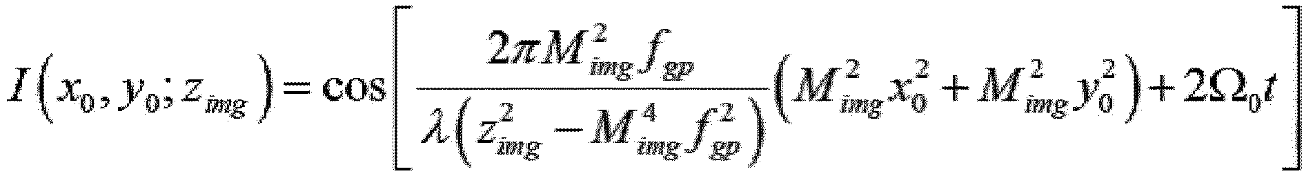
여기서, Mimg는 편광 감응형 렌즈(기하 위상 렌즈) 면의 패턴을 대상물 면으로 이미징할 때 이미징 렌즈에 의한 상의 축소 또는 확대 비율, zimg는 제2 구면파의 초점위치로부터 대상물까지의 거리이다.
그 밖에도, 본 발명의 실시예는 편광 감응형 렌즈(1140)와 스캔수단(1160) 사이에 제2 렌즈(미도시)를 위치시켜, 평면파와 구면파 간의 간섭 패턴을 형성시킬 수 있다.
일반적으로 광 스캐닝 홀로그래피에서는 구면파와 평면파가 간섭된 선형 프레넬 윤대판으로 물체를 스캐닝하여 물체의 홀로그램을 획득한다. 기하 위상 렌즈와 물체 사이에 렌즈를 위치시키면 평면파와 구면파의 간섭 패턴을 형성시킬 수 있다. 따라서, 구면파와 평면파의 간섭에 의해 형성된 간섭 패턴인 선형 프레넬 윤대판으로 인코딩된 홀로그램을 얻을 수 있다.
이를 구체적으로 설명하면 다음과 같다. 이때 설명의 편의상 도 5의 355번 부호 자리에 제1 렌즈 대신 제2 렌즈가 배치된 것을 가정하여 설명한다.
제2 렌즈(미도시)는 편광 감응형 렌즈(1140)와 스캔수단(1160) 사이에 배치되되, 제2 구면파와 동일한 초점 위치(f2)에 초점이 형성되도록 배치된다. 이와 같이, 제2 렌즈(미도시)의 초점위치와 제2 구면파의 초점위치가 동일하게 되면, 제2 구면파는 평면파로 변환되고 제1 구면파는 구면파의 곡률이 제2 렌즈에 의해 추가된다.
이 경우, 간섭 빔은 제1 구면파와 평면파 간의 간섭에 의해 형성되는 선형 프레넬 윤대판 형태로서 아래의 수학식 5으로 정의될 수 있다.

여기서, z는 제2 렌즈에 의해 곡률이 더해진 제1 구면파의 초점위치로부터 대상물까지의 거리이다.
이와 같이, 제2 렌즈의 초점위치가 제2 구면파의 초점위치와 같도록 제2 렌즈를 삽입 배치할 경우, 구면파와 평면파 간의 간섭 패턴인 선형 프레넬 윤대판에 의해 인코딩된 홀로그램을 얻을 수 있다.
도 6은 본 발명에 따른 인라인 스캐닝 홀로그래피 시스템의 제4 실시예를 나타낸 도면이다.
도 6에 나타낸 것과 같이, 제4 실시예에 따른 인라인 스캐닝 홀로그래피 시스템(1400)은 편광기(1110), 선편광 방향 변환기(1120), 신호 생성부(1225), 콜리메이터(1130), 편광 감응형 렌즈(1140), 편광기(1150), 제1 렌즈(1355), 스캔 수단(1160), 집광기(1170), 제1 광 검출기(1175), 전자처리부(1280)를 포함한다.
이러한 도 6은 제2 실시예에 따른 도 4의 구성에 앞서 상술한 제1 렌즈(1355)(또는 제2 렌즈)가 조합된 구조에 해당하므로 그에 대한 중복된 설명은 생략한다.
한편, 상술한 본 발명의 실시예들은 편광 감응형 렌즈로 기하 위상 렌즈를 사용한 것을 예시하고 있으나, 액정으로 형성된 편광 감응성(polarization sensitive) 투과형(transmission) 액정(liquid crystal) GRIN(graded index lens) 등과 같이, 편광에 따라 초점거리를 달리하는 다양한 렌즈를 사용할 수 있다.
구체적인 예로, p-편광 방향에 대해 정렬된 액정으로 구성되어 p-편광된 빛은 굴절시키고 s-편광된 빛은 통과시키는 편광 감응성 투과형 액정 GRIN 렌즈를 카르타시안 좌표계의 x-방향으로 정렬하여 위치시키고, 편광 감응성 투과형 액정 GRIN 렌즈와 편광기(1150) 사이에 1/4 파장판을 삽입할 수 있다. 이 경우 광원으로부터 출력된 빛은 편광기(1110)를 통해 선편광되어 가변 파장판(1121)에 전달되며, 가변 파장판(1121)에서 편광 방향이 변경된 선편광 빔은 콜리메이터(1130)에서 확장된 후 편광 감응성 투과형 액정 GRIN 렌즈를 통과하면서 p-편광 방향에 해당하는 부분은 구면파를 형성하고, s-편광 방향에 해당하는 부분은 평면파를 형성한다. 이때, 편광 감응성 투과형 액정 GRIN 렌즈와 편광기(1150) 사이에 삽입된 1/4 파장판에 의해, p-편광 부분의 구면파와 s-편광 부분의 평면파를 각각 우현 원편광과 좌현 원편광으로 변환하며, 변환된 빔은 편광기(1150)를 통과함으로써 수학식 5와 같이 평면파와 구면파의 간섭에 의해 형성된 간섭 패턴인 선형 프레넬 윤대판을 형성할 수 있다.
또한, 수학식 3 내지 5의 비선형 프레넬 윤대판과 역 곡률의 프레넬 윤대판을 형성하기 위해, 설명의 편의상 기하 위상 렌즈와 대상물 사이에 렌즈(제1 또는 제2 렌즈)를 삽입하는 것으로 설명하였으나, 콜리메이터(1130)와 편광 감응형 렌즈(1140) 사이 부분에 렌즈를 삽입하여 위치시키는 방식으로 수학식 3 내지 5를 형성할 수 있음은 물론이다.
또한, 도 1 및 도 5에 도시된 제1 및 제3 실시예의 경우 함수 발생기에서 가변 파장판(1121)의 변조 신호로 Ω(t)를 생성하여 가변 파장판(1121)에 전달하고, 헤테로다인 기준신호로 sin(12Ω(t))를 생성하여 헤테로다인 검출기(1181)에 전달하였으나, 후술하는 도 7과 같이 빔 스플리터 및 제2 광 검출기를 이용하여 헤테로다인 기준신호를 생성할 수도 있다.
도 7은 본 발명에 따른 인라인 스캐닝 홀로그래피 시스템의 제5 실시예를 나타낸 도면이다.
도 7에 나타낸 것과 같이, 제5 실시예에 따른 인라인 스캐닝 홀로그래피 시스템(1500)은 편광기(1110), 선편광 방향 변환기(1120), 신호 생성부(1125), 콜리메이터(1130), 편광 감응형 렌즈(1140), 편광기(1150), 스캔 수단(1160), 집광기(1170), 제1 광 검출기(1175), 빔 스플리터(1565), 제2 광 검출기(1566), 전자처리부(1180)를 포함한다.
이러한 도 7은 도 1의 구성에 빔 스플리터(1565) 및 제2 광 검출기(1566)가 부가된 경우에 해당한다. 빔 스플리터(1565)는 편광기(1150)와 스캔수단(1160) 사이에 설치되어, 편광기(1150)를 통과한 빔의 일부를 투과시켜 스캔수단(1160)에 전달하고 나머지를 반사시킨다.
제2 광 검출기(1566)는 빔 스플리터(1565)에 의한 반사되는 빔의 경로 상에 위치하여, 빔 스플리터(1565)로부터 반사된 빔을 검출한다. 물론 빔 스플리터(1565)로부터 반사된 빔은 제2 집광기(1567)에 의해 공간적으로 집적된 후 제2 광 검출기(1566)에서 검출된다.
이러한 제2 광 검출기(1566)는 반사된 빔을 검출하여 이를 기초로 비팅 신호 sin(12Ω(t))을 생성한다. 비팅 신호는 앞서 사용된 헤테로다인 기준 신호와 동일한 것을 알 수 있다. 따라서 제2 광 검출기(1566)는 비팅신호를 기준 신호로 하여 헤테로다인 검출기(1181)에 입력할 수 있다.
이러한 제5 실시예의 경우 신호 생성부(1525)는 주기적 램프 신호 Ω(t)를 생성하여 선편광 방향 변환기(1120)에 인가하며, 제2 광 검출기(1566)는 반사된 빔을 기초로 생성한 헤테로다인 기준 신호 sin(12Ω(t))를 전자처리부(1180)의 헤테로다인 검출기(1181)로 인가하면 된다.
상술한 제1 내지 제5 실시예는 대상체(1010)로부터 반사된 빛을 집광하는 것으로 설명하였으나, 대상체(1010)가 형광하는 형광체인 경우 대상체(1010)로부터 형광된 빛을 제1 집광기(1170)를 이용하여 집광하여 제1 광검출기(1175)에 전달하고 제1 광 검출기(1175)는 제1 집광기(1170)를 통해 공간적으로 집적된 빔을 검출하여 형광체의 홀로그램을 레코딩할 수 있다. 이때, 제1 광검출기(1175)와 대상체(1010) 사이에 대상체(1010)로부터 형광된 빛의 파장에 해당하는 빛을 필터링해서 제1 광검출기(1175)에 전달하도록 하는 이색성 거울(dichroic mirror)을 포함한 광학 필터를 위치시켜, 광학 노이즈를 저감할 수 있다.
또한, 대상물(1010)이 빛을 투과하는 투과형 대상물(1010)인 경우 대상물(1010)을 투과한 빛의 경로에 제1 집광기(1170)와 제1 광검출기(1175)를 위치시켜, 대상물을 투과한 빛을 제1 집광기(1170)를 이용해 집광하여 제1 광검출기(1175)에 전달하고, 제1 광 검출기(1175)는 제1 집광기(1170)를 통해 공간적으로 집적된 빔을 검출하여 투과형 대상물(1010)의 홀로그램을 레코딩할 수 있다.
또한, 제1 내지 제5 실시예에서 제1 광검출기(1175)와 대상체(1010) 사이에 푸리에 렌즈(Fourier lens)와, 푸리에 렌즈의 초점에 위치한 핀홀(pin-hole)로 구성된 공간 필터(spatial filter)를 각각 위치시켜 대상체(1010)로부터 반사 또는 투과된 빛을 공간적으로 필터링하면, 대상체(1010)의 위상 분포를 포함한 홀로그램을 얻을 수 있다.
이상과 같은 본 발명에 따른 인라인 스캐닝 홀로그래피 시스템에 의하면, 편광 감응형 렌즈를 이용하여 단일의 광 경로에서 스캐닝 패턴을 형성함에 따라 고효율 및 고품질의 광 스캐닝 홀로그래피를 구현할 수 있음은 물론 높은 안정성 및 낮은 복잡도의 광학계 구조를 사용하여 외부 환경에 강인하고 안정적인 이점이 있다.
다음은 도 8 내지 도 11을 참조하여 기하 위상 스캐닝 홀로그래피 시스템을 설명한다.
기하 위상 스캐닝 홀로그래피 시스템은, 기하 위상 검출 방식을 이용함에 따라, 광 신호를 변조하기 위한 복잡한 변조 장치 없이도, 쌍영상 잡음과 배경 잡음이 제거된 실제 물체의 복소수 홀로그램을 획득할 수 있는 구조를 제안한다.
도 8은 본 발명에 따른 기하 위상 스캐닝 홀로그래피 시스템의 제1 실시예를 나타낸 도면이다.
도 8에 나타낸 것과 같이, 제1 실시예에 따른 인라인 스캐닝 홀로그램 장치(2100)는 편광 빔스플리터(2110), 제1 및 제2 1/4 파장판(2115,2120), 제1 및 제2 콜리메이터(2125,2130), 제1 렌즈(2135), 제1 빔스플리터(2140), 스캔수단(2145), 집광기(2150), 제2 빔스플리터(2155), 제1 및 제2 편광기(2160a,2160b), 제1 및 제2 광검출기(2170a,2170b), 전자처리부(2180)를 포함한다.
우선, 광원으로부터 출력된 선편광(linearly polarized) 빔은 제1 거울(M1)에 전달되고, 제1 거울(M1)은 전달받은 선편광 빔을 편광 빔스플리터(2110)(polarizing beam splitter)에 입시사킨다.
편광 빔스플리터(2110)는 입사되는 선편광 빔을 서로 직교하는 p-편광의 제1 빔 및 s-편광의 제2 빔으로 분리한다.
편광 빔스플리터(2110)에 전달되는 빔의 도파 방향에 대해 수직한 평면에 대하여 상호 직교하는 편광 부분을 나누어, 편광 빔스플리터(2110)가 투과시키는 편광을 p-편광이라 하고, 반사시키는 편광을 s-편광이라 한다.
p-편광의 축 방향은 편광 빔스플리터(2110)와 제1 1/4 파장판(2115) 사이의 경로 상에 양방향 화살표로 도시하였고, s-편광의 축 방향은 편광 빔스플리터(2110)와 제2 1/4 파장판(2120) 사이의 경로 상에 p-편광의 축 방향에 직교한 방향의 양방향 화살표로 도시하였다.
여기서, 선편광 빔의 편광 방향을 p-편광 축에 대해 45도 회전된 방향으로 위치시켜, 편광 빔스플리터(2110)에 p-편광의 방향에 대해 45로 회전된 방향을 갖는 선편광 빔이 전달된다. 따라서 선편광 빔은 편광 빔스플리터(2110)의 p-편광 축에 대해 45도 회전된 편광 방향으로 입사된다.
편광 빔스플리터(2110)는 전달받은 선편광 빔 중 p-편광 부분을 통과시켜 제1 1/4 파장판(2115)으로 전달하고, s-편광 부분을 반사시켜 제2 1/4 파장판(2120)으로 전달한다. 제1 및 제2 1/4 파장판(2115,2120)(quarter wave plate)은 입사되는 빔의 편광을 변경한다.
제1 1/4 파장판(2115)은 p-편광의 제1 빔을 좌현 원편광 빔(left-handed circular polarized beam)으로 변환하여 제2 거울(M2)로 전달하고, 제2 1/4 파장판(2120)은 s-편광의 제2 빔을 우현 원편광 빔(right-handed circular polarized beam)으로 변환하여 제3 거울(M3)로 전달한다.
제2 거울(M2)은 전달받은 좌현 원편광 빔을 빔 확장기인 제1 콜리메이터(2125)로 전달하고, 제3 거울(M3)은 전달받은 우현 원편광 빔을 제2 콜리메이터(2130)로 전달한다.
제1 콜리메이터(2125)는 좌현 원편광 빔을 콜리메이션하여 평면파를 형성시켜 제1 빔스플리터(2140)로 전달한다. 즉, 제1 콜리메이터(2125)는 좌현 원편광 빔을 확장하여 좌현 원편광의 평면파를 제1 빔스플리터(2140)로 제공한다.
제2 콜리메이터(2130)는 우현 원편광 빔을 콜리메이션하여 평면파를 형성시켜 제1 렌즈(2135)로 전달한다. 즉, 제2 콜리메이터(2130)는 우현 원편광 빔을 확장하여 우현 원편광의 평면파를 제1 렌즈(2135)로 제공한다. 여기서, 제1 렌즈(2135)는 우현 원편광의 평면파를 다시 구면파로 변환하여 제1 빔스플리터(2140)로 제공한다.
좌현 원편광의 평면파와 우현 원편광의 구면파는 제1 빔스플리터(2140)의 일면과 타면을 통해 각각 들어와 서로 중첩된다. 즉, 제1 빔스플리터(2140)는 좌현 원편광의 평면파와 우현 원편광의 구면파를 상호 중첩시켜 간섭 빔을 형성하며, 형성한 간섭 빔을 스캔수단(2145)으로 전달한다.
이때, 간섭 빔은 기하 위상 프레넬 윤대판(Geometric Phase Fresnel Zone Plate) 형태로서 아래의 수학식 6으로 정의될 수 있다.
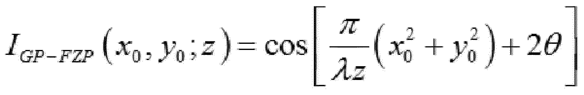
여기서, λ는 사용된 빔의 파장, (x0
2+y0
2)는 빔의 광축에 직교하는 평면을 (x0,y0)로 하는 카타르시안 좌표계, z는 상기 구면파의 초점위치로부터 대상물까지의 거리, θ는 편광 빔스플리터의 p-편광 축에 대해 시계 방향으로 선편광된 각도를 나타낸다.
즉, 도 8의 제1 빔스플리터(2140)를 통해 중첩된 우현 원평광된 구면파와 좌현 원편광된 평면파 중에서 편광 빔스플리터(2110)의 p-편광 축에 대해서 시계방향으로 θ의 각을 갖는 축 방향으로 선편광된 부분의 간섭 패턴은 위상이 2θ 만큼 천위된 프레넬 윤대판(Fresnel zone plate)이 된다. 이때, 편광축의 기하적인 회전각에 의해 간섭패턴의 위상이 천위되므로, 이러한 형태를 기하 위상 프레넬 윤대판(Geometrical Phase Fresnel Zone Plate)이라 한다.
스캔수단(2145)은 제1 빔스플리터(2140)로부터 전달받은 간섭 빔을 이용하여 대상물을 스캔한다. 스캔수단(2145)은 이러한 간섭 빔을 응답지령빔으로 하여 촬영 대상물(이하, 대상물)(2010)을 스캔한다.
대상물을 스캔하기 위한 응답지령빔의 세기 패턴은 수학식 7과 같이 정의될 수 있다.

여기서, dc는 구면파 세기 패턴과 평면파 세기 패턴의 합으로, 이상적인 경우에는 공간에 따른 변화가 없고 실제의 경우에도 공간에 따른 변화가 아주 작은 직류 바이어스(direct current bias) 성분이다.
본 실시예에서 스캔수단(2145)은 거울 스캐너를 사용한다. 거울 스캐너는 대상물(2010)을 X 방향으로 스캔하는 수평 스캔 거울과, Y 방향으로 스캔하는 수직 스캔 거울을 갖는 X-Y 스캐너로 구성된다. 물론, 본 발명의 경우 스캔수단(2145)이 거울 스캐너로 한정되는 것은 아니며 이와 유사한 수단 또는 공지된 다른 스캔수단이 사용될 수도 있다.
본 발명의 실시예는 거울 형태의 스캔수단(2145)에 우현 원편광된 구면파와 좌현 원편광된 평면파가 중첩된 빔이 전달되고, 스캔수단(2145)은 기하 위상 프레넬 윤대판을 대상물을 가로질러 이동시킴에 따라, 대상물을 스캐닝할 수 있도록 한다.
스캔수단(2145)은 전자처리부(2180)에 마련된 스캔 제어부(2185)로부터 스캐닝 제어신호를 받아 동작되며, 스캔 제어부(2185)는 스캔수단(2145)의 스캐닝 위치를 제어하기 위한 스캐닝 제어신호를 발생시킨다. 여기서, 스캐닝 제어신호는 수평 스캔 거울 및 수직 스캔 거울을 수평 방향 및 수직 방향으로 각각 제어하기 위한 수평 스캔 신호 및 수직 스캔 신호를 포함할 수 있다.
물론, 이렇게 거울 스캐너를 이용하는 대신 대상물을 대물판 위에 위치시키고, 대물판을 수평 이동하여 대상물을 스캔할 수 있음은 물론이다. 본 발명은 이외에도 전자광 편향기(electrooptic deflector)를 이용하는 등 다양한 방법을 이용하여 대상물을 스캔할 수 있다.
스캔수단(2145)에 의해 지정되는 스캔 빔의 스캔 위치에서 대상물(2010)로부터 반사된 빔은 집광기(2150)에 의해서 공간적(spatially)으로 집적(integrated)된다.
여기서, 집광기(2150)는 렌즈를 통해 구현될 수 있으며, 이외에도 오목 반사경을 포함한 영상(imaging) 또는 비 영상(non-imaging) 집광기 등의 공지된 다양한 집광수단으로 구현될 수 있다.
집광기(2150)에 의해 집광된 빔은 제2 빔스플리터(2155)로 전달된다. 제2 빔스플리터(2155)는 집광기(2150)로부터 집광된 빔을 전달받아 제1 및 제2 출력 빔으로 분리한다. 제2 빔스플리터(2155)는 집광기(2150)에 의해 집광된 빛 중 일부를 통과시켜 제1 편광기(2160a)로 전달하고, 일부를 반사시켜 제2 편광기(2160b)로 전달한다. 즉, 통과된 제1 출력 빔은 제1 편광기(2160a)로, 반사된 출력 제2 빔은 제2 편광기(2160b)로 전달된다.
제1 및 제2 편광기(2160a,2160b)는 전달받은 제1 및 제2 출력 빔을 각각 편광시킨다. 여기서, 제2 편광기(2160b)는 제1 편광기(2160a)의 편광 방향을 기준으로 시계 방향으로 45도 회전된 편광 방향으로 위치시킨다.
제1 편광기(2160a)는 제2 빔스플리터(2155)로부터 전달받은 제1 출력 빔 중 제1 편광기(2160a)의 편광 방향으로 편광된 빔을 투과시켜 제1 광검출기(2170a)로 전달한다. 마찬가지로, 제2 편광기(2160b)는 전달받은 제2 출력 빔 중 제2 편광기(2160b)의 편광 방향으로 편광된 빔을 투과시켜 제2 광검출기(2170b)로 전달한다.
제1 및 제2 광검출기(2170a,2170b)는 제1 및 제2 편광기(2160a,2160b)에 대응하여 설치되며, 제1 및 제2 편광기(2160a,2160b)를 통과한 각각의 출력 빔을 검출한다.
제1 및 제2 광검출기(2170a,2170b)는 광 다이오드로 구현될 수 있으나, 본 발명이 반드시 이에 한정되지 않으며, 광증배관(photo-multiplier tube) 등 다양한 광 검출수단이 적용될 수 있다. 또한, 집광기 없이도 광 검출수단의 검출 면으로 전달되어 들어오는 빛을 직접 검출할 수도 있다.
제1 및 제2 광검출기(2170a,2170b)는 집광기(2150)를 통해 공간적으로 집적된 빔 중 제1 편광기(2160a)의 방향으로 편광된 편광 부분과 제2 편광기(2160b) 방향으로 편광된 편광 부분을 검출하여 전류 신호로 변환하는데, 편광 부분의 세기에 따라 전류를 생성한다.
즉, 제1 및 제2 광검출기(2170a,2170b)는 제1 및 제2 편광기(2160a,2160b)를 통과한 제1 및 제2 출력 빔의 세기에 대응하여 제1 및 제2 전류 신호를 생성한다.
스캔수단(2145)에 의해 지정되는 스캔 빔의 스캔 위치에 대해 제1 광검출기(2170a)에서 생성된 제1 전류신호는 제1 편광기 방향의 기하 위상 프레넬 윤대판과 대상물의 3차원 영상분포가 인코드된 패턴에 해당하고, 제2 광검출기(2170b)에서 생성된 제2 전류신호는 제2 편광기 방향의 기하 위상 프레넬 윤대판과 대상물의 3차원 영상분포가 인코드된 패턴에 해당한다.
제2 편광기(2160b)의 편광 방향은 제1 편광기(2160a)의 편광 방향을 기준으로 시계 방향으로 45도 회전되어 있다. 따라서, 제1 및 제2 광검출기에서 각각 생성한 제1 및 제2 전류 신호( ,
,  )는 제1 편광기(2160a)의 편광 방향을 기준으로 아래의 수학식 8과 수학식 9와 같이 정의될 수 있다.


여기서, O(x0,y0;z)는 대상물의 반사율(reflectance)에 대한 3차원 분포로서 대상물의 3차원 영상이며,  는 콘볼루션(convolution) 연산, λ는 사용된 빔의 파장, (x,y)는 스캔수단에 의해 지정되는 스캔 빔의 스캔 위치, z는 구면파의 초점위치로부터 대상물까지의 거리(대상물의 깊이 위치), dc는 직류 바이어스 성분이다.
이러한 수학식 8과 수학식 9에 의한 제1 및 제2 전류 신호는 전자처리부(2180) 내의 제1 및 제2 dc 제거 필터(2181a,2181b)로 각각 전달된다.
전자처리부(2180)는 제1 및 제2 광검출기에서 검출된 제1 및 제2 전류 신호를 처리하여 대상물의 복소수 홀로그램을 생성하며, 제1 및 제2 dc 제거 필터(2181a,2181b), AD 컨버터(2182), 신호처리부(2183), 저장부(2184) 및 스캔 제어부(2185)를 포함한다.
제1 및 제2 dc 제거 필터(2181a,2181b)는 제1 및 제2 전류 신호로부터 각각 직류 바이어스 성분 즉, dc 성분을 제거하여 AD 컨버터(2182)에 입력시킨다.
제1 및 제2 dc 제거 필터(2181a,2181b)는 수학식 8, 9에서 dc와 대상물의 반사율 분포가 콘볼루션된 부분을 제거하여 아래의 수학식 10, 11과 같은 신호를 출력으로 생성하여 AD 컨버터(2182)로 전달한다.


AD 컨버터(2182)는 각각의 필터를 통해 dc 성분이 필터링된 제1 및 제2 전류 신호를 디지털 신호로 변환한다. 이러한 AD 컨버터(2182)는 두 개의 입력 채널을 가지며 수학식 10의 동위상 신호와 수학식 11의 π/2 위상 신호를 각 채널을 통해 입력받아 디지털 신호로 변환한다.
신호처리부(2183)는 변환된 디지털 신호로부터 대상물의 복소수 홀로그램을 생성하고, 저장부(2184)는 생성된 복소수 홀로그램을 저장한다.
이때 복소수 홀로그램은 아래의 수학식 12와 같이 정의될 수 있다.

여기서,  는
는  로부터 dc 성분을 제거한 상태의 값,
  는
는  로부터 dc 성분을 제거한 상태의 값을 나타낸다.
스캔 제어부(2185)는 대상물의 임의 위치에 대한 홀로그램 처리가 완료될 때마다 스캔수단(2145)의 위치를 변경시키는 제어 신호를 생성하여 스캔수단(2145)으로 전달한다. 물론, 이를 위해, 신호처리부(2183)는 수학식 1O과 11을 수학식 12와 같이 복소수 더하기 방법으로 더하여 각각의 스캔 위치에 대한 2차원 배열을 형성하고 저장부(2184)는 이를 저장한다.
여기서, 제1 및 제2 dc 제거 필터(2181a,2181b)를 생략하는 대신, AD 컨버터(2182)가 제1 및 제2 광검출기(2170a,2170b)의 출력을 받아서 이를 디지털 신호로 변환 후 디지털 신호처리 방식을 통해 dc 제거 필터링을 수행할 수도 있다.
이외에도, 신호처리부(2183)는 수학식 10, 11에 대하여 각각의 스캔 위치에 따른 2차원 배열을 형성하여 저장부(2184)로 전달한 다음, 스캔이 종료되면 저장부(2184)로부터 읽어들여 수학식 10, 11에 대응하는 2차원 배열을 수학식 12의 복소수 더하기 방법으로 더한 후 다시 저장부(2184)에 저장할 수 있다.
여기서 수학식 12는 종래의 광 스캐닝 홀로그램을 이용하여 획득한 복소수 홀로그램과 동일한데, 이는 곧 복잡한 광 변조기를 사용하지 않고도 기존과 동일한 형태의 홀로그램을 생성할 수 있음을 의미한다.
본 발명의 제1 실시예에서는 선편광 빔을 편광 빔스플리터(2110)를 통해 p-편광과 s-편광으로 분리한 다음 제1 1/4파장판(2115)과 제2 1/4 파장판(2120)을 이용하여 우현 원편광 빔과 좌현 원편광 빔을 생성하였으나, 본 발명이 반드시 이에 한정되지 않으며, 공지된 다양한 간섭수단을 이용하여 우현 원편광과 좌현 원편광을 생성할 수 있다.
도 9는 도 8의 변형 예를 나타낸 도면이다. 이러한 도 9는 좌현 원편광 빔과 우현 원편광 빔을 생성하는 다른 실시예를 나타낸다.,
도 9의 경우 도 8의 편광 빔스플리터(2110), 제1 1/4파장판(2115) 및 제2 1/4파장판(2120)을 제거하는 대신, 편광 빔스플리터(2110)의 위치에는 편광에 무관한 빔스플리터(2111)를 위치시키고, 제2 1/4 파장판(2120)의 위치에는 1/2 파장판(2121)(half wave plate)을 위치시키며, 광원에서는 선편광 빔이 아닌 좌현 원편광 빔을 생성하여 빔스플리터(2111)로 전달한다.
빔스플리터(2111)는 광원으로부터 입사되는 좌현 원편광 빔의 일부를 투과시켜 제2 거울(M2)에 전달하고 일부를 반사시켜 1/2 파장판(2121)에 전달한다. 1/2 파장판(2121)은 전달받은 좌현 원편광 빔을 우현 원편광 빔으로 변환하여 제3 거울(M3)로 전달한다. 즉, 이와 같은 방식을 통해서도 우현 원편광 빔과 좌현 원편광 빔을 생성할 수 있다. 이후의 동작은 앞서 도 8의 원리와 동일하다.
도 10은 본 발명에 따른 기하 위상 스캐닝 홀로그래피 시스템의 제2 실시예를 나타낸 도면이다.
도 10에 나타낸 것과 같이, 제2 실시예에 따른 기하 위상 스캐닝 홀로그래피 시스템(2200)은 편광 빔스플리터(2110), 제1 및 제2 1/4 파장판(2115,2120), 제1 및 제2 콜리메이터(2125,2130), 제1 렌즈(2135), 제1 빔스플리터(2140), 스캔수단(2145), 집광기(2150), 제2 빔스플리터(2155), 제1 및 제2 편광기(2160a,2160b), 제1 및 제2 광검출기(2170a,2170b), 전자처리부(2180), 제2 렌즈(2390)를 포함한다.
이러한 도 10의 제2 실시예는 도 8에 의한 제1 실시예의 구조에서 제1 빔스플리터(2140)와 대상물 사이에 제2 렌즈(2390)를 추가로 삽입한 것이다. 따라서 도 10에서 도 8의 제1 실시예의 경우와 동일한 부호를 갖는 구성요소는 동일한 동작을 수행함을 의미하므로, 동일한 부호의 구성요소에 대한 별도의 설명은 생략한다.
도 10의 경우 제2 렌즈(2390)는 제1 빔스플리터(2140)와 스캔수단(2145) 사이에 위치하며, 제1 콜리메이터(2125)에서 생성된 좌현 원편광의 평면파를 제1 구면파로 변환한다. 이때, 제1 빔스플리터(2140)에서 형성되는 간섭 빔은 서로 다른 초점 위치를 갖는 좌현 원편광의 구면파와 우현 원편광의 구면파 간의 중첩에 의해 형성되는 비선형 프레넬 윤대판 형태를 가지게 된다.
구체적으로, 제2 렌즈(2390)는 제1 콜리메이터(2125)에서 생성된 좌현 원편광의 평면파를 제1 구면파로 변환하여 대상물로 전달하며, 제2 콜리메이터(2130)와 제1 렌즈(2135)에 의해 형성된 우현 원편광의 제2 구면파의 초점 위치를 대상물 쪽으로 전달한다.
이때, 제2 렌즈(2390)를 통과하여 형성된 제1 구면파의 제1 초점의 위치와, 제1 렌즈(2135)를 통과하여 초점 위치가 변경된 제2 구면파의 제2 초점의 위치가 대상물과 제2 렌즈(2390) 사이에 위치할 경우, 대상물을 스캔하는 스캔 빔은 서로 다른 초점 위치를 갖는 발산하는 두 구면파의 중첩에 의해 비선형 프레넬 윤대판이 된다.
또한, 비선형 윤대판을 이용하여 대상물을 스캔하고 대상물로부터 반사된 빔을 제1 실시예의 경우와 같이 집광하여 처리하면 대상물의 비선형 홀로그램을 획득하여 저장부에 저장할 수 있다. 저장부에 저장된 비선형 홀로그램은 수학식 13과 같이 표현된다.

여기서, d는 제1 구면파의 초점과 제2 구면파의 초점 사이의 거리이다. 비선형 홀로그램의 경우 본 출원인에 의한 한국공개특허 제2013-0081127호(22013.07.16 공개)에 따라 d를 조정하여 축소 및 확대에 따른 왜곡을 보정할 수 있다. d는 렌즈의 이미징 법칙에 따라 제2 렌즈(2390)의 위치와 초점거리를 변경하여 조정할 수 있다.
또한, 대상물을 제1 구면파의 초점위치와 제2 구면파의 초점위치 사이에 위치시키는 경우, 발산하는 구면파와 수렴하는 구면파의 역 방향 곡률의 간섭에 의해 형성된 패턴으로 인코드된 물체의 홀로그램을 획득하고 수치적으로 복원하여 분해능을 향상시킬 수 있다. 이는 수학식 14와 같이 주어진다.

다음은 본 발명의 제3 실시예를 설명한다. 제3 실시예는 추가적인 광검출기를 부가하여 제1 및 제2 dc 제거 필터(2181a,2181b) 사용 없이도 dc 성분을 제거함은 물론 노이즈에 강건한 홀로그램을 획득하는 방식이다.
도 11은 본 발명에 따른 기하 위상 스캐닝 홀로그래피 시스템의 제3 실시예를 나타낸 도면이다.
도 11에 나타낸 것과 같이, 제3 실시예에 따른 기하 위상 스캐닝 홀로그래피 시스템(2300)은 편광 빔스플리터(2110), 제1 및 제2 1/4 파장판(2115,2120), 제1 및 제2 콜리메이터(2125,2130), 제1 렌즈(2135), 제1 빔스플리터(2140), 스캔수단(2145), 집광기(2150), 제2 내지 제4 빔스플리터(2455a,2455b,2455c), 제1 내지 제4 편광기(2460a,2460b,2460c,2460d), 제1 내지 제4 광검출기(2470a,2470b,2470c,2470d), 전자처리부(2480)를 포함한다.
이러한 도 11의 제3 실시예는 도 8의 제1 실시예의 구조에서 집광 부분의 구성이 변경된 것이다. 따라서 도 11에서 도 8의 제1 실시예와 동일한 부호를 갖는 구성요소는 동일한 동작을 수행함을 의미하므로, 동일한 부호의 구성요소에 대한 별도의 설명은 생략한다.
이하에서는 집광기(2150) 이후의 구성 부분을 중점적으로 설명한다.
제2 빔스플리터(2455a)는 집광기(2150)에서 집광된 빔을 입사받아 제1 및 제2 출력 빔으로 분리한다. 제2 빔스플리터(2455a)에서 투과된 제1 출력 빔은 제3 빔스플리터(2455b)로, 반사된 제2 출력 빔은 제4 빔스플리터(2455c)에 전달된다.
제3 빔스플리터(2455b)는 제1 출력 빔을 다시 제1a 및 제1b 출력 빔으로 분리한다. 제3 빔스플리터(2455b)에서 투과된 제1a 출력 빔은 제1 편광기(2460a)로 전달되고, 반사된 제1b 출력 빔은 제2 편광기(2460b)로 전달된다.
제4 빔스플리터(2455c)는 제2 출력 빔을 다시 제2a 및 제2b 출력 빔으로 분리한다. 제4 빔스플리터(2455c)에서 투과된 제2a 출력 빔은 제3 편광기(2460c)로 전달되고, 반사된 제2b 출력 빔은 제4 편광기(2460d)로 전달된다.
이때, 제2, 제3 및 제4 편광기(2460b,2460c,2460d)는 각각 제1 편광기(2460a)의 편광 방향을 기준으로 시계 방향으로 45도, 90도, 135도 회전된 편광 방향을 가진다.
제1 내지 제4 광검출기(2470a,2470b,2470c,2470d)는 제1 내지 제4 편광기(2460a,2460b,2460c,2460d)에 각각 대응하여 설치되어, 제1 내지 제4 편광기(2460a,2460b,2460c,2460d)를 통과한 각각의 출력 빔을 검출한다.
여기서, 제1 내지 제4 광검출기(2470a,2470b,2470c,2470d)는 앞서 제1 실시예와 같이, 제1 내지 제4 편광기(2460a,2460b,2460c,2460d)를 통과한 각각의 출력 빔의 세기에 대응하여 제1 내지 제4 전류 신호를 각각 생성한다.
검출된 제1 내지 제4 전류 신호는 제n 전류 신호( )로 명명하며, 아래의 수학식 15와 같이 정의될 수 있다.

여기서, n={1,2,3,4}로, 제1,2,3,4 광검출기에 각각 대응하는 인덱스이다.
또한, pn은 n으로 지정된 n번째 광검출기에서 각각 생성된 홀로그램 신호의 천위된 위상, O(x0,y0;z)는 대상물의 반사율에 대한 3차원 분포로서 대상물의 3차원 영상이며,  는 콘볼루션(convolution) 연산, λ는 사용된 빔의 파장, (x,y)는 스캔수단(2145)에 의해 지정되는 스캔 빔의 스캔 위치, z는 구면파의 초점위치로부터 대상물까지의 거리이다.
이러한 수학식 15에 의한 제1 내지 제4 전류 신호는 각각 전자처리부(2480) 내의 AD 컨버터(2482)로 전달된다.
전자처리부(2480)는 제1 내지 제4 광검출기에서 검출된 제1 내지 제4 전류신호를 처리하여 대상물의 복소수 홀로그램을 생성하며, AD 컨버터(2482), 신호처리부(2483), 저장부(2484) 및 스캔 제어부(2485)를 포함한다.
AD 컨버터(2482)는 제1 내지 제4 전류 신호를 디지털 신호로 변환한다. AD 컨버터(2482)는 4개의 입력 채널을 가지며 수학식 15의 0 위상, π/2 위상, π 위상, 3π/2 위상를 각 채널을 통해 입력받아 디지털 신호로 변환한다. 변환된 디지털 전류신호는 스캔수단(2145)의 스캐닝 위치와 함께 신호처리부(2483)로 제공된다.
신호처리부(2483)는 변환된 디지털 신호로부터 대상물의 복소수 홀로그램을 생성하고, 저장부(2484)는 생성된 복소수 홀로그램을 저장한다.
이때 복소수 홀로그램은 아래의 수학식 16과 같이 정의될 수 있다.

스캔 제어부(2485)는 대상물의 임의 위치에 대한 홀로그램 처리가 완료될 때마다 스캔수단(2145)의 위치를 변경시키는 제어 신호를 생성하여 스캔수단(2145)으로 전달한다. 물론, 이를 위해, 신호처리부(2483)는 수학식 15에 의한 각각의 위상에 따른 신호를 수학식 16과 같이 복소수 더하기 방법으로 더하여 각각의 스캔 위치에 대한 2차원 배열을 형성하고 저장부(2484)는 이를 저장한다.
이외에도, 신호처리부(2483)는 수학식 15의 각 위상에 따른 신호에 대하여 각각의 스캔 위치에 따른 2차원 배열을 형성하여 저장부(2484)로 전달한 다음, 스캔이 종료되면 저장부(2484)로부터 읽어들여 수학식 15의 각각의 위상에 따른 신호에 대응하는 2차원 배열을 수학식 16의 복소수 더하기 방법으로 더한 후 다시 저장부(2484)에 저장할 수 있다.
다음은 본 발명의 제4 실시예에 관하여 설명한다. 본 발명의 제4 실시예는 제3 실시예의 도면인 도 11에서 점선 박스 내의 제4 빔 스플리터(2455c), 제4 편광기(2460d), 제4 광검출기(2470d)를 제거한 경우이다.
이때, 제2 및 제3 빔스플리터(2455a,2455b)의 동작은 제3 실시예와 동일하다. 제3 실시예와 다른 점은 제2 빔스플리터(2455a)에서 반사된 제2 출력 빔이 제3 편광기(2460c)에 전달되어 편광되며, 제3 편광기(2460c)를 통해 편광된 빔은 제3 광검출기(2470c)에서 검출된다.
이러한 제4 실시예의 경우 제1,제2,제3 광검출기(2470a,2470b,2470c)에서 출력된 3개의 전류 신호를 3개 채널을 갖는 AD 컨버터를 이용하여 디지털 신호로 변환하여 신호 처리부에 전달하고, 신호 처리부는 이를 수학식 17의 방법으로 처리하여 복소수 홀로그램을 얻을 수 있다.

이상과 같은 본 발명에 따른 기하 위상 스캐닝 홀로그래피 시스템에 따르면, 광 신호를 변조하기 위한 복잡한 변조 장치의 사용 없이 편광에 따른 기하학적 구조를 이용하여 쌍영상 잡음과 배경 잡음이 없는 실제 물체의 복소수 홀로그램을 획득할 수 있어 구조의 복잡도를 낮출 수 있고 소형 및 경량화가 가능함은 물론, 에너지 소비에 민감한 모바일 기기에도 적용 가능한 이점을 제공한다.
다음은 도 12 내지 도 20을 참조하여 기하 위상 인라인 스캐닝 홀로그래피 시스템을 설명한다.
기하 위상 인라인 스캐닝 홀로그래피 시스템은, 편광 감응형 렌즈를 이용하여 단일의 광 경로에서 스캐닝 패턴을 형성함에 따라 높은 안정성 및 낮은 복잡도를 가지며, 기하 위상 검출 방식을 이용함에 따라 복잡한 변조 장치 없이도 쌍영상 잡음과 배경 잡음이 제거된 실제 물체의 복소수 홀로그램을 획득할 수 있다.
도 12는 본 발명에 따른 기하 위상 인라인 스캐닝 홀로그래피 시스템의 제1 실시예를 나타낸 도면이다.
도 12에 나타낸 것과 같이, 제1 실시예에 따른 기하 위상 인라인 스캐닝 홀로그래피 시스템(3100)은 편광기(3110), 콜리메이터(3120), 편광 감응형 렌즈(3130), 스캔수단(3140), 집광기(3150), 제1 빔스플리터(3155), 제1 및 제2 편광기(3160a,3160b), 제1 및 제2 광검출기(3170a,3170b), 전자처리부(3180)를 포함한다.
먼저, 광원은 전자기파를 발생시킨다. 본 발명의 실시예에서 광원으로는 가간섭 광을 출력하는 레이저 발생기, 그리고 가간섭성이 낮은 LED(light emitting diode) 램프, 결맞음 길이(coherence length)가 짧은 헬로겐 램프 등의 다양한 수단이 사용 가능하다.
편광기(3110)(linear polarizer)는 입력된 광원을 선편광 빔(linearly polarized light)으로 변환하여 콜리메이터(3120)로 제공한다. 도 12에서 광원 및 편광기(3110)는 생략될 수 있으며 이 경우 외부에서 만들어진 선편광 빔이 콜리메이터(3120)로 바로 입력될 수 있다. 또한, 도 12에서 광원이 생략되는 경우에는 외부에서 제공된 광원이 편광기(3110)로 바로 입력될 수 있다.
콜리메이터(3120)(collimator)는 편광기(3110)에서 출력된 빔을 확장시켜 편광 감응형 렌즈(3130)로 전달하며, 빔을 확장할 수 있는 다양한 수단으로 구현될 수 있다.
편광 감응형 렌즈(3130)(polarization sensitive lens)는 콜리메이터(3120)를 통해 확장된 선편광 빔을 입사받아, 음의 초점거리를 갖는 우현 원편광의 제1 구면파 및 양의 초점거리를 갖는 좌현 원편광의 제2 구면파를 동시에 생성한다.
여기서, 편광 감응형 렌즈(3130)는 기하 위상 렌즈(geometric phase lens)로 구성될 수 있다. 편광 감응형 렌즈(3130)는 액정(liquid crystal)에 기반한 판카랏남 상(Pancharatnam-phase) 효과를 갖는 얇은 평판형 구조이며, 입력된 빛의 편광에 따라 입력 빔의 파면을 양과 음의 초점거리를 갖는 파면으로 변경하는 렌즈 역할을 한다. 기하 위상 렌즈는 공지된 것과 같이 마하젠더 간섭계 기반의 아날로그 홀로그램 레코딩 장치를 이용하여 제작될 수 있으며, 예를 들어 ImagineOptix사에서 제공하는 기성품을 사용할 수 있다.
도 13은 본 발명의 실시예에 따른 편광 감응형 렌즈의 원리를 설명하는 도면이다.
도 13의 (a)와 같이, 기하 위상 렌즈(편광 감응형 렌즈; 3130)는 우현 원편광(right-handed circular polarized beam)이 입사되면 해당 편광 방향에 감응하여 볼록 렌즈로 작용하여 양의 초점거리(+fgp)를 갖는 좌현 원편광(left-handed circular polarized beam)의 구면파를 만들고, 도 13의 (b)와 같이 좌현 원편광이 입사되면 해당 편광 방향에 감응하여 오목 렌즈로 작용하여 음의 초점거리(-fgp)를 갖는 우현 원편광의 구면파를 만든다.
다만, 본 발명의 실시예의 경우, 도 13의 (c)와 같이, 선편광(linearly polarized)의 파면이 기하 위상 렌즈에 입력되는데, 이 경우 기하 위상 렌즈는 입력된 빛의 에너지 세기를 거의 절반씩 나누어 음의 초점거리(-fgp)를 갖는 우현 원편광의 구면파(이하, 제1 구면파)와 양의 초점거리(+fgp)를 갖는 좌현 원편광의 구면파(이하, 제2 구면파)의 파면을 동시에 생성한다.
이처럼, 편광 감응형 렌즈(3130)는 입사된 선편광 빔의 일부를 우현 원 편광으로 변경하여 입사되는 빔의 진행 방향과 반대 쪽에 초점을 위치시키는 제1 구면파를 형성하고, 이와 동시에 나머지를 좌현 원 편광으로 변경하여 입사되는 빔의 진행 방향 쪽에 초점을 위치시키는 제2 구면파를 형성한다.
이와 같이, 본 발명의 실시예는 편광 감응형 렌즈를 이용하여 단일의 광 경로에서 스캐닝 패턴을 형성함에 따라, 광원을 두 경로로 분리 후 재결합하여 간섭 패턴을 형성하는 종래 기법보다 더욱 고효율 및 고품질의 광 스캐닝 홀로그래피를 구현할 수 있음은 물론, 높은 안정성 및 낮은 복잡도의 광학계 구조를 사용하여 외부 환경에 강인하고 안정적인 이점이 있다.
편광 감응형 렌즈(3130)에서 인라인(In-Line)으로 도출된 제1 및 제2 구면파는 스캔수단(3140)으로 전달된다. 여기서 제1 구면파와 제2 구면파는 인라인 구조 상에서 상호 중첩되면서 간섭 빔을 형성하게 된다.
스캔수단(3140)은 제1 및 제2 구면파 사이에서 발생한 간섭 빔을 이용하여 대상물을 스캔한다.
이때, 간섭 빔은 기하 위상 프레넬 윤대판(Geometric Phase Fresnel Zone Plate) 형태로서 아래의 수학식 18로 정의될 수 있다.

여기서, λ는 사용된 빔의 파장, fgp는 상기 편광 감응형 렌즈의 초점거리, (x0
2+y0
2)는 선편광 빔의 광축에 직교하는 평면을 (x0,y0)로 하는 카타르시안 좌표계, z는 제2 구면파의 초점위치로부터 대상물까지의 거리, θ는 편광기(3110)의 편광 축에 대해 시계 방향으로 선편광된 각도를 나타낸다.
즉, 도 12의 편광 감응형 렌즈(3140)를 통해 생성된 제1 구면파와 제2 구면파 중에서 편광기(3110)의 편광 축에 대해서 시계방향으로 θ의 각을 갖는 축 방향으로 선편광된 부분의 간섭 패턴은 위상이 2θ 만큼 천위된 비선형 프레넬 윤대판이 된다. 이때, 편광축의 기하적인 회전각에 의해 간섭패턴의 위상이 천위되므로, 이러한 형태를 기하 위상 프레넬 윤대판(Geometrical Phase Fresnel Zone Plate)이라 한다.
스캔수단(3140)은 편광 감응형 렌즈(3130)로부터 전달받은 간섭 빔을 이용하여 대상물을 스캔한다. 스캔수단(3140)은 이러한 간섭 빔을 응답지령빔으로 하여 촬영 대상물(이하, 대상물)을 스캔한다.
대상물을 스캔하기 위한 응답지령빔의 세기 패턴은 수학식 19와 같이 정의될 수 있다.

여기서, dc는 구면파 세기 패턴과 구면파 세기 패턴의 합으로, 이상적인 경우에는 공간에 따른 변화가 없고 실제의 경우에도 공간에 따른 변화가 아주 작은 직류 바이어스(direct current bias) 성분이다.
본 실시예에서 스캔수단(3140)은 거울 스캐너를 사용한다. 거울 스캐너는 대상물(3010)을 X 방향으로 스캔하는 수평 스캔 거울과, Y 방향으로 스캔하는 수직 스캔 거울을 갖는 X-Y 스캐너로 구성된다. 물론, 본 발명의 경우 스캔수단(3140)이 거울 스캐너로 한정되는 것은 아니며 이와 유사한 수단 또는 공지된 다른 스캔수단이 사용될 수도 있다.
본 발명의 실시예는 거울 형태의 스캔수단(3140)에 우현 원편광된 구면파와 좌현 원편광된 구면파가 중첩된 빔이 전달되고, 스캔수단(3140)은 기하 위상 프레넬 윤대판을 대상물을 가로질러 이동시킴에 따라, 대상물을 스캐닝할 수 있도록 한다.
스캔수단(3140)은 전자처리부(3180)에 마련된 스캔 제어부(3185)로부터 스캐닝 제어신호를 받아 동작되며, 스캔 제어부(3185)는 스캔수단(3140)의 스캐닝 위치를 제어하기 위한 스캐닝 제어신호를 발생시킨다. 여기서, 스캐닝 제어신호는 수평 스캔 거울 및 수직 스캔 거울을 수평 방향 및 수직 방향으로 각각 제어하기 위한 수평 스캔 신호 및 수직 스캔 신호를 포함할 수 있다.
물론, 이렇게 거울 스캐너를 이용하는 대신 대상물을 대물판 위에 위치시키고, 대물판을 수평 이동하여 대상물을 스캔할 수 있음은 물론이다. 본 발명은 이외에도 전자광 편향기(electrooptic deflector)를 이용하는 등 다양한 방법을 이용하여 대상물을 스캔할 수 있다.
스캔수단(3140)에 의해 지정되는 스캔 빔의 스캔 위치에서 대상물(3010)로부터 반사된 빔은 집광기(3150)에 의해서 공간적(spatially)으로 집적(integrated)된다.
여기서, 집광기(3150)는 렌즈를 통해 구현될 수 있으며, 이외에도 오목 반사경을 포함한 영상(imaging) 또는 비 영상(non-imaging) 집광기 등의 공지된 다양한 집광수단으로 구현될 수 있다.
집광기(3150)에 의해 집광된 빔은 제1 빔스플리터(3155)로 전달된다. 제1 빔스플리터(3155)는 집광기(3150)로부터 집광된 빔을 전달받아 제1 및 제2 출력 빔으로 분리한다. 제1 빔스플리터(3155)는 집광기(3150)에 의해 집광된 빛 중 일부를 통과시켜 제1 편광기(3160a)로 전달하고, 일부를 반사시켜 제2 편광기(3160b)로 전달한다. 즉, 통과된 제1 출력 빔은 제1 편광기(3160a)로, 반사된 출력 제2 빔은 제2 편광기(3160b)로 전달된다.
제1 및 제2 편광기(3160a,3160b)는 전달받은 제1 및 제2 출력 빔을 각각 편광시킨다. 여기서, 제2 편광기(3160b)는 제1 편광기(3160a)의 편광 방향을 기준으로 시계 방향으로 45도 회전된 편광 방향으로 위치시킨다.
제1 편광기(3160a)는 제1 빔스플리터(3155)로부터 전달받은 제1 출력 빔 중 제1 편광기(3160a)의 편광 방향으로 편광된 빔을 투과시켜 제1 광검출기(3170a)로 전달한다. 마찬가지로, 제2 편광기(3160b)는 전달받은 제2 출력 빔 중 제2 편광기(3160b)의 편광 방향으로 편광된 빔을 투과시켜 제2 광검출기(3170b)로 전달한다.
제1 및 제2 광검출기(3170a,3170b)는 제1 및 제2 편광기(3160a,3160b)에 대응하여 설치되며, 제1 및 제2 편광기(3160a,3160b)를 통과한 각각의 출력 빔을 검출한다.
제1 및 제2 광검출기(3170a,3170b)는 광 다이오드로 구현될 수 있으나, 본 발명이 반드시 이에 한정되지 않으며, 광증배관(photo-multiplier tube) 등 다양한 광 검출수단이 적용될 수 있다. 또한, 집광기 없이도 광 검출수단의 검출 면으로 전달되어 들어오는 빛을 직접 검출할 수도 있다.
제1 및 제2 광검출기(3170a,3170b)는 집광기(3150)를 통해 공간적으로 집적된 빔 중 제1 편광기(3160a)의 방향으로 편광된 편광 부분과 제2 편광기(3160b) 방향으로 편광된 편광 부분을 검출하여 전류 신호로 변환하는데, 편광 부분의 세기에 따라 전류를 생성한다.
즉, 제1 및 제2 광검출기(3170a,3170b)는 제1 및 제2 편광기(3160a,3160b)를 통과한 제1 및 제2 출력 빔의 세기에 대응하여 제1 및 제2 전류 신호를 생성한다.
스캔수단(3140)에 의해 지정되는 스캔 빔의 스캔 위치에 대해 제1 광검출기(3170a)에서 생성된 제1 전류신호는 제1 편광기 방향의 기하 위상 프레넬 윤대판과 대상물의 3차원 영상분포가 인코드된 패턴에 해당하고, 제2 광검출기(3170b)에서 생성된 제2 전류신호는 제2 편광기 방향의 기하 위상 프레넬 윤대판과 대상물의 3차원 영상분포가 인코드된 패턴에 해당한다.
제2 편광기(3160b)의 편광 방향은 제1 편광기(3160a)의 편광 방향을 기준으로 시계 방향으로 45도 회전되어 있다. 따라서, 제1 및 제2 광검출기(3170a,3170b)에서 각각 생성한 제1 및 제2 전류 신호( ,
,  )는 제1 편광기(3160a)의 편광 방향을 기준으로 아래의 수학식 20과 수학식 21과 같이 정의될 수 있다.


여기서, O(x0,y0;z)는 대상물의 반사율에 대한 3차원 분포로서 대상물의 3차원 영상이며,  는 콘볼루션(convolution) 연산, λ는 사용된 빔의 파장, (x,y)는 스캔수단에 의해 지정되는 스캔 빔의 스캔 위치, fgp는 편광 감응형 렌즈의 초점거리, z는 제2 구면파의 초점위치로부터 대상물까지의 거리(대상물의 깊이 위치), dc는 직류 바이어스 성분을 나타낸다.
이러한 수학식 20과 수학식 21에 의한 제1 및 제2 전류 신호는 전자처리부(3180) 내의 제1 및 제2 dc 제거 필터(3181a,3181b)로 각각 전달된다.
전자처리부(3180)는 제1 및 제2 광검출기(3170a,3170b)에서 검출된 제1 및 제2 전류 신호를 처리하여 대상물의 복소수 홀로그램을 생성하며, 제1 및 제2 dc 제거 필터(3181a,3181b), AD 컨버터(3182), 신호처리부(3183), 저장부(3184) 및 스캔 제어부(3185)를 포함한다.
제1 및 제2 dc 제거 필터(3181a,3181b)는 제1 및 제2 전류 신호로부터 각각 직류 바이어스 성분 즉, dc 성분을 제거하여 AD 컨버터(3182)에 입력시킨다.
제1 및 제2 dc 제거 필터(3181a,3181b)는 수학식 20, 21에서 dc와 대상물의 반사율 분포가 콘볼루션된 부분을 제거하여 아래의 수학식 22, 23과 같은 신호를 출력으로 생성하여 AD 컨버터(3182)로 전달한다.


AD 컨버터(3182)는 각각의 필터를 통해 dc 성분이 필터링된 제1 및 제2 전류 신호를 디지털 신호로 변환한다. 이러한 AD 컨버터(3182)는 두 개의 입력 채널을 가지며 수학식 22의 동위상 신호와 수학식 23의 π/2 위상 신호를 각 채널을 통해 입력받아 디지털 신호로 변환한다.
신호처리부(3183)는 변환된 디지털 신호로부터 대상물의 복소수 홀로그램을 생성하고, 저장부(3184)는 생성된 복소수 홀로그램을 저장한다.
이때 복소수 홀로그램은 아래의 수학식 24와 같이 정의될 수 있다.

여기서,  는
는  로부터 dc 성분을 제거한 상태의 값,
  는
는  로부터 dc 성분을 제거한 상태의 값을 나타낸다.
스캔 제어부(3185)는 대상물의 임의 위치에 대한 홀로그램 처리가 완료될 때마다 스캔수단(3140)의 위치를 변경시키는 제어 신호를 생성하여 스캔수단(3140)으로 전달한다. 신호처리부(3183)는 수학식 22와 23을 수학식 24와 같이 복소수 더하기 방법으로 더하여 각각의 스캔 위치에 대한 2차원 배열을 형성하고 저장부(3184)는 이를 저장한다.
여기서, 제1 및 제2 dc 제거 필터(3181a,3181b)를 생략하는 대신, AD 컨버터(3182)가 제1 및 제2 광검출기(3170a,3170b)의 출력을 받아서 이를 디지털 신호로 변환 후 디지털 신호처리 방식을 통해 dc 제거 필터링을 수행할 수도 있다.
이외에도, 신호처리부(3183)는 수학식 22, 23에 대하여 각각의 스캔 위치에 따른 2차원 배열을 형성하여 저장부(3184)로 전달한 다음, 스캔이 종료되면 저장부(3184)로부터 읽어들여 수학식 22, 23에 대응하는 2차원 배열을 수학식 24의 복소수 더하기 방법으로 더한 후 다시 저장부(3184)에 저장할 수 있다.
여기서 수학식 24는 종래의 광 스캐닝 홀로그램을 이용하여 획득한 복소수 홀로그램과 동일한데, 이는 곧 복잡한 광 변조기를 사용하지 않고도 복잡한 간섭계 구조 없이 인라인 구조를 통하여 기존과 동일한 형태의 홀로그램을 생성할 수 있음을 의미한다. 이러한 도 12의 구성은 추후 도 14, 도 17 및 도 18로 응용될 수 있다.
도 14는 본 발명에 따른 기하 위상 인라인 스캐닝 홀로그래피 시스템의 제2 실시예를 나타낸 도면이다.
도 14에 나타낸 것과 같이, 제2 실시예에 따른 기하 위상 인라인 스캐닝 홀로그래피 시스템(3200)은 편광기(3110), 콜리메이터(3120), 편광 감응형 렌즈(3130), 제1 렌즈(3235), 스캔수단(3140), 집광기(3150), 제1 빔스플리터(3155), 제1 및 제2 편광기(3160a,3160b), 제1 및 제2 광검출기(3170a,3170b), 전자처리부(3180)를 포함한다.
이러한 도 14는 도 12의 제1 실시예의 구조에서 제1 렌즈(3235)가 추가로 삽입된 것을 나타내며, 동일한 부호의 구성요소에 대한 별도의 설명은 생략한다.
도 14에서 제1 렌즈(3235)는 편광 감응형 렌즈(3130)와 스캔수단(3140) 사이에 설치되어 제1 및 제2 구면파의 각 초점 간의 거리를 조정하고, 편광 감응형 렌즈 면의 패턴을 대상물 영역의 면으로 이미징하는 이미징 렌즈 역할을 한다.
즉, 기하 위상 렌즈 면을 제1 렌즈(3235)를 이용하여 확대 또는 축소하는 방식으로 대상물의 영역에 이미징하면, 기하 위상 렌즈 면에서의 패턴이 대상물에 이미징되어 투사될 수 있다.
제1 구면파의 초점 위치는 f1, 제2 구면파의 초점위치는 f2라 할 때, 도 12의 경우 f1과 f2 위치 간의 거리는 2fgp 였지만, 도 14의 경우 f1과 f2 위치 간의 거리는 제1 렌즈(3235)의 축소 또는 확대율에 따라 2M2
imgfgp로 변경된다.
또한 이러한 도 14의 경우, 간섭 빔은 기하 위상 비선형 프레넬 윤대판 형태로서, 아래의 수학식 25로 정의될 수 있다.

여기서, Mimg는 편광 감응형 렌즈(기하 위상 렌즈) 면의 패턴을 대상물 영역의 면으로 이미징 시 제1 렌즈(3235)에 의한 상의 축소 또는 확대 비율, zimg는 제2 구면파의 초점위치로부터 대상물까지의 거리, 2M2
imgfgp는 조정된 제1 및 제2 구면파의 각 초점 간의 거리이다.
이와 같이 편광 감응형 렌즈(3130)와 대상물(3010) 사이에 제1 렌즈(3235)를 위치시켜 확대 또는 축소의 방법으로 두 구면파의 초점 간 거리가 변경된 새로운 제1 및 제2 구면파를 대상물의 면에 위치시킬 수 있다.
여기서 상술한 본 발명의 실시예들은 두 구면파가 모두 발산하는 영역에 물체를 위치시킨 것을 예시하지만, 헤테로다인 스캐닝 기반 홀로그램의 현미경 응용에 있어 분해능을 향상시키기 위한 방법을 이용하여, 두 구면파의 초점 사이(f1과 f2 위치 사이 지점)에 물체를 위치시킬 수도 있다.
이를 위해, 편광 감응형 렌즈(기하 위상 렌즈)와 대상물 사이에 이미징 렌즈를 위치시켜, 제1 구면파의 초점 위치(f1)를 대상물의 전면에 위치시키고 제2 구면파의 초점 위치(f2)를 대상물의 후면에 위치시키는 방식을 사용하여, 발산하는 구면파와 수렴하는 구면파의 역 방향 곡률의 간섭 패턴에 의해 인코딩된 물체의 홀로그램을 획득할 수 있으며, 이를 수치적으로 복원하여 분해능을 향상시킬 수 있다.
예를 들면, 기하 위상 렌즈와 대상물 사이에 이미징 렌즈를 위치시켜, 기하 위상 렌즈 면을 대상물 면에 이미징하면 수렴하는 제1 구면파와 발산하는 제2 구면파의 간섭 패턴으로 인코딩된 홀로그램을 얻을 수 있으며, 이 경우 간섭 패턴은 아래의 수학식 26과 같이 정의될 수 있다.
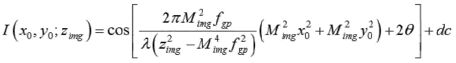
여기서, Mimg는 편광 감응형 렌즈(기하 위상 렌즈) 면의 패턴을 대상물 면으로 이미징할 때 이미징 렌즈에 의한 상의 축소 또는 확대 비율, zimg는 제2 구면파의 초점위치로부터 대상물까지의 거리이다.
그 밖에도, 본 발명의 실시예는 편광 감응형 렌즈(3130)와 스캔수단(3140) 사이에 제2 렌즈(미도시)를 위치시켜, 평면파와 구면파 간의 간섭 패턴을 형성시킬 수 있다.
일반적으로 광 스캐닝 홀로그래피에서는 구면파와 평면파가 간섭된 선형 프레넬 윤대판으로 물체를 스캐닝하여 물체의 홀로그램을 획득한다. 기하 위상 렌즈와 물체 사이에 렌즈를 위치시키면 평면파와 구면파의 간섭 패턴을 형성시킬 수 있다. 따라서, 구면파와 평면파의 간섭에 의해 형성된 간섭 패턴인 선형 프레넬 윤대판으로 인코딩된 홀로그램을 얻을 수 있다.
이를 구체적으로 설명하면 다음과 같다. 이때 설명의 편의상 도 14의 235번 부호 자리에 제1 렌즈 대신 제2 렌즈가 배치된 것을 가정하여 설명한다.
제2 렌즈(미도시)는 편광 감응형 렌즈(3130)와 스캔수단(3140) 사이에 배치되되, 제2 구면파와 동일한 초점 위치(f2)에 초점이 형성되도록 배치된다. 이와 같이, 제2 렌즈(미도시)의 초점위치와 제2 구면파의 초점위치가 동일하게 되면, 제2 구면파는 평면파로 변환되고 제1 구면파는 구면파의 곡률이 제2 렌즈에 의해 추가된다.
이 경우, 간섭 빔은 제1 구면파와 평면파 간의 간섭에 의해 형성되는 선형 프레넬 윤대판 형태로서 아래의 수학식 27로 정의될 수 있다.

여기서, z는 제2 렌즈에 의해 곡률이 더해진 제1 구면파의 초점위치로부터 대상물까지의 거리이다.
이와 같이, 제2 렌즈의 초점위치가 제2 구면파의 초점위치와 같도록 제2 렌즈를 삽입 배치할 경우, 구면파와 평면파 간의 간섭 패턴인 선형 프레넬 윤대판에 의해 인코딩된 홀로그램을 얻을 수 있다.
다음은 본 발명의 제3 실시예를 설명한다. 제3 실시예는 제1 실시예에 추가적인 광검출기를 부가하여, 제1 및 제2 dc 제거 필터(3181a,3181b) 사용 없이도 dc 성분을 제거함은 물론, 노이즈에 강건한 홀로그램을 획득하는 방식이다.
도 15는 본 발명에 따른 기하 위상 인라인 스캐닝 홀로그래피 시스템의 제3 실시예를 나타낸 도면이다.
도 15에 나타낸 것과 같이, 제3 실시예에 따른 기하 위상 인라인 스캐닝 홀로그래피 시스템(3300)은 편광기(3110), 콜리메이터(3120), 편광 감응형 렌즈(3130), 스캔수단(3140), 집광기(3150), 제1 내지 제3 빔스플리터(3355a,3355b,3355c), 제1 내지 제4 편광기(3360a,3360b,3360c,3360d), 제1 내지 제4 광검출기(3370a,3370b,3370c,3370d), 전자처리부(3380)를 포함한다.
이러한 도 15의 제3 실시예는 도 12의 제1 실시예의 구조에서 집광 부분의 구성이 변경된 것이다. 따라서 도 15에서 도 12의 제1 실시예와 동일한 부호를 갖는 구성요소는 동일한 동작을 수행함을 의미하므로, 동일한 부호의 구성요소에 대한 별도의 설명은 생략한다. 또한, 이러한 도 15의 구성은 추후 도 17, 도 19 및 도 20으로 응용될 수 있다.
이하에서는 집광기(3150) 이후의 구성 부분을 중점적으로 설명한다.
제1 빔스플리터(3355a)는 집광기(3150)에서 집광된 빔을 입사받아 제1 및 제2 출력 빔으로 분리한다. 제1 빔스플리터(3355a)에서 투과된 제1 출력 빔은 제2 빔스플리터(3355b)로, 반사된 제2 출력 빔은 제3 빔스플리터(3355c)에 전달된다.
제2 빔스플리터(3355b)는 제1 출력 빔을 다시 제1a 및 제1b 출력 빔으로 분리한다. 제2 빔스플리터(3355b)에서 투과된 제1a 출력 빔은 제1 편광기(3360a)로 전달되고, 반사된 제1b 출력 빔은 제2 편광기(3360b)로 전달된다.
제3 빔스플리터(3355c)는 제2 출력 빔을 다시 제2a 및 제2b 출력 빔으로 분리한다. 제3 빔스플리터(3355c)에서 투과된 제2a 출력 빔은 제3 편광기(3360c)로 전달되고, 반사된 제2b 출력 빔은 제4 편광기(3360d)로 전달된다.
이때, 제2, 제3 및 제4 편광기(3360b,3360c,3360d)는 각각 제1 편광기(3360a)의 편광 방향을 기준으로 시계 방향으로 45도, 90도, 135도 회전된 편광 방향을 가진다.
제1 내지 제4 광검출기(3370a,3370b,3370c,3370d)는 제1 내지 제4 편광기(3360a,3360b,3360c,3360d)에 각각 대응하여 설치되어, 제1 내지 제4 편광기(3360a,3360b,3360c,3360d)를 통과한 각각의 출력 빔을 검출한다.
여기서, 제1 내지 제4 광검출기(3370a,3370b,3370c,3370d)는 앞서 제1 실시예와 같이, 제1 내지 제4 편광기(3360a,3360b,3360c,3360d)를 통과한 각각의 출력 빔의 세기에 대응하여 제1 내지 제4 전류 신호를 각각 생성한다.
검출된 제1 내지 제4 전류 신호는 제n 전류 신호( )로 명명하며, 아래의 수학식 28과 같이 정의될 수 있다.

여기서, n={1,2,3,4}로, 제1,2,3,4 광검출기에 각각 대응하는 인덱스이다.
또한, pn은 n으로 지정된 n번째 광검출기에서 각각 생성된 홀로그램 신호의 천위된 위상, O(x0,y0;z)는 대상물의 반사율에 대한 3차원 분포로서 대상물의 3차원 영상이며,  는 콘볼루션(convolution) 연산, λ는 사용된 빔의 파장, (x,y)는 스캔수단(3140)에 의해 지정되는 스캔 빔의 스캔 위치, fgp는 편광 감응형 렌즈의 초점거리, z는 제2 구면파의 초점위치로부터 대상물까지의 거리이다.
이러한 수학식 28에 의한 제1 내지 제4 전류 신호는 각각 전자처리부(3380) 내의 AD 컨버터(3382)로 전달된다.
전자처리부(3380)는 제1 내지 제4 광검출기에서 검출된 제1 내지 제4 전류신호를 처리하여 대상물의 복소수 홀로그램을 생성하며, AD 컨버터(3382), 신호처리부(3383), 저장부(3384) 및 스캔 제어부(3385)를 포함한다.
AD 컨버터(3382)는 제1 내지 제4 전류 신호를 디지털 신호로 변환한다. AD 컨버터(3382)는 4개의 입력 채널을 가지며 수학식 28의 0 위상, π/2 위상, π 위상, 3π/2 위상를 각 채널을 통해 입력받아 디지털 신호로 변환한다. 변환된 디지털 전류신호는 스캔수단(3140)의 스캐닝 위치와 함께 신호처리부(3383)로 제공된다.
신호처리부(3383)는 변환된 디지털 신호로부터 대상물의 복소수 홀로그램을 생성하고, 저장부(3384)는 생성된 복소수 홀로그램을 저장한다.
이때 복소수 홀로그램은 아래의 수학식 29와 같이 정의될 수 있다.
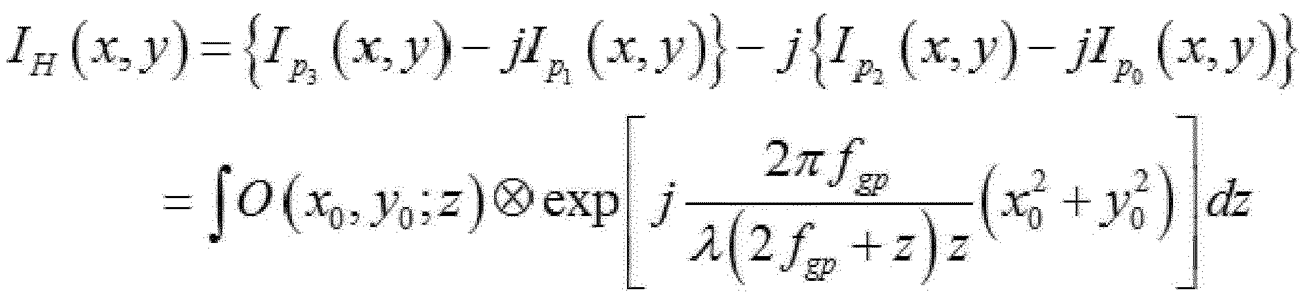
스캔 제어부(3385)는 대상물의 임의 위치에 대한 홀로그램 처리가 완료될 때마다 스캔수단(3140)의 위치를 변경시키는 제어 신호를 생성하여 스캔수단(3140)으로 전달한다. 물론, 이를 위해, 신호처리부(3383)는 수학식 28에 의한 각각의 위상에 따른 신호를 수학식 29와 같이 복소수 더하기 방법으로 더하여 각각의 스캔 위치에 대한 2차원 배열을 형성하고 저장부(3384)는 이를 저장한다.
이외에도, 신호처리부(3383)는 수학식 28의 각 위상에 따른 신호에 대하여 각각의 스캔 위치에 따른 2차원 배열을 형성하여 저장부(3384)로 전달한 다음, 스캔이 종료되면 저장부(3384)로부터 읽어들여 수학식 28의 각각의 위상에 따른 신호에 대응하는 2차원 배열을 수학식 29의 복소수 더하기 방법으로 더한 후 다시 저장부(3384)에 저장할 수 있다.
다음은 제3 실시예에 대한 변형 예를 설명한다. 이는 제3 실시예의 도면인 도 15에서 점선 박스 내의 제3 빔스플리터(3355c), 제4 편광기(3360d), 제4 광검출기(3370d)를 제거한 경우이다.
이때, 제1 및 제2 빔스플리터(3355a,3355b)의 동작은 제3 실시예와 동일하다. 제3 실시예와 다른 점은 제1 빔스플리터(3355a)에서 반사된 제2 출력 빔이 제3 편광기(3360c)에 바로 전달되어 편광되며, 제3 편광기(3360c)를 통해 편광된 빔은 제3 광검출기(3370c)에서 검출된다.
이러한 변형예의 경우 제1,제2,제3 광검출기(3370a,3370b,3370c)에서 출력된 3개의 전류 신호를 3개 채널을 갖는 AD 컨버터를 이용하여 디지털 신호로 변환하여 신호 처리부에 전달하고, 신호 처리부는 이를 수학식 30의 방법으로 처리하여 복소수 홀로그램을 얻을 수 있다.

이상과 같은 본 발명에 따르면, 광 신호를 변조하기 위한 복잡한 변조 장치의 사용 없이 편광에 따른 기하학적 구조를 이용하여 쌍영상 잡음과 배경 잡음이 없는 실제 물체의 복소수 홀로그램을 획득할 수 있어 구조의 복잡도를 낮출 수 있고 소형 및 경량화가 가능함은 물론, 에너지 소비에 민감한 모바일 기기에도 적용 가능하다.
도 16은 본 발명에 따른 기하 위상 인라인 스캐닝 홀로그래피 시스템의 제4 실시예를 나타낸 도면이다.
도 16은 도 15의 제3 실시예의 구조에서 편광 감응형 렌즈(3130)와 스캔수단(3140) 사이에 렌즈(3435)가 추가로 삽입된 것으로, 그 원리는 앞서 도 14의 경우와 같으며, 동일 구성요소에 대한 별도의 설명은 생략한다. 이와 같이, 렌즈(3435)를 추가 삽입할 경우 앞서 수학식 25 내지 수학식 27과 같은 효과를 얻을 수 있다.
이하에서는 기하 위상 인라인 스캐닝 홀로그래피 시스템의 진동, 광원의 요동, 광정렬 오류 등에 따라, 스캔수단(3140)에 의해 지정되는 스캔 빔의 스캔 위치에서 발생되는 위상 요동(phase fluctuation)을 상쇄하여, 위상 요동에 더욱 강건한 홀로그램을 획득하기 위한 기법을 제시한다.
도 17은 본 발명에 따른 기하 위상 인라인 스캐닝 홀로그래피 시스템의 제5 실시예를 나타낸 도면이다. 이러한 도 17의 경우 도 12의 제1 실시예의 구조에 대해 위상 요동 보상 기능이 부가된 것이다.
도 17에 나타낸 것과 같이, 제5 실시예에 따른 기하 위상 인라인 스캐닝 홀로그래피 시스템(3500)은 편광기(3110), 콜리메이터(3120), 편광 감응형 렌즈(3130), 스캔수단(3140), 제1 집광기(3150), 제1 빔스플리터(3155), 제1 및 제2 편광기(3160a,3160b), 제1 및 제2 광검출기(3170a,3170b), 전자처리부(3180-1), 제2 빔스플리터(3590), 제2 집광기(3595), 그리고 R-집광부("R" 표기 요소)를 포함한다.
이러한 도 17은 시스템(3500)의 진동에 의한 위상 요동을 보정하도록, 도 12의 제1 실시예의 구조에서 제2 빔스플리터(3590), 제2 집광기(3595), 그리고 R-집광부("R" 표기 요소)가 추가적으로 삽입된 것을 나타낸다. 나머지 동일한 부호의 구성요소에 대한 별도의 설명은 생략한다.
우선, 도 17은 도 12와 비교할 때, 편광 감응형 렌즈(3130)와 스캔수단(3140) 사이에 제2 빔스플리터(3590)가 추가로 배치된 것을 알 수 있다.
제2 빔스플리터(3590)는 편광 감응형 렌즈(3130)에 의해 만들어진 간섭 빔의 일부분을 투과시켜 대상물의 스캔에 사용하도록 하고 일부를 반사시켜 R-집광부로 전달하는 역할을 한다.
즉, 제2 빔스플리터(3590)는 일측에 입사되는 간섭 빔의 일부를 투과시켜 타측의 스캔수단(3140)으로 전달하고 일부를 반사시켜 하측의 제2 집광기(3595)로 전달한다. 이때, 제2 집광기(3595)는 제2 빔스플리터(3590)에서 반사된 간섭 빔을 공간적으로 집적한다. 이러한 제2 집광기(3595)는 제1 집광기(3150)와 동일한 소자로 구현될 수 있다.
제2 집광기(3595)에 의해 집광된 빔은 R-집광부로 전달된다. R-집광부는 제2 빔스플리터(3590)에서 반사된 빔을 처리한다. 여기서, R-집광부(3155-R + 3160a-R,3160b-R + 3170a,3170b)는 제1 집광기(3150)의 후단에 위치한 요소(3155 + 3160a,3160b + 3170a,3170b)와 대칭되는 형태로 배치된다.
구체적으로, R-집광부는 제1 집광기(3150)의 후단에 위치한 제1 빔스플리터(3155), 제1 및 제2 편광기(3160a,3160b), 제1 및 제2 광검출기(3170a,3170b)와 각각 대칭 형태로 배치되는 제1-R 빔스플리터(3155-R), 제1-R 및 제2-R 편광기(3160a-R,3160b-R), 그리고 제1-R 및 제2-R 광검출기(3170a-R,3170b-R)를 포함한다.
R-집광부 내부 요소들에 의한 빔의 분리, 편광, 검출 원리는 앞서 상술한 것과 동일하므로 상세한 설명은 생략한다. 이와 같이, R-집광부의 마지막 경로인 제1-R 및 제2-R 광검출기(3170a-R,3170b-R)를 통해 검출된 빔은 전자처리부(3180-1)로 전달된다.
전자처리부(3180-1)는 제1-R 및 제2-R 광검출기(3170a-R,3170b-R)에서 검출된 제1-R 및 제2-R 전류 신호를 시스템(3500)의 진동에 의한 위상 요동을 보상하기 위한 제1 및 제2 위상 보정 기준 신호로 사용한다.
또한, 도 17의 전자처리부(3180-1)는 도 12와 비교하면, 제1 및 제2 dc 제거 필터(3181a,3181b)와 함께 제1-R 및 제2-R dc 제거 필터(3181c,3181d)를 추가로 포함한다.
즉, 앞서 도 12의 제1 실시예에서 대상물로부터 반사된 빔을 집광하여 검출된 제1 및 제2 전류 신호에 대해 신호 처리 전 제1 및 제2 dc 제거 필터(3181a,3181b)를 통해 dc 제거를 수행하였듯이, 도 17의 제5 실시예는 스캔수단(3140)의 전단에서 간섭 빔을 집광하여 검출한 제1-R 및 제2-R 전류 신호(이하, 제1 및 제2 위상 보정 기준 신호)로부터 제1-R 및 제2-R dc 제거 필터(3181c,3181d)를 통해 dc 성분을 제거하는 과정을 추가로 포함한다.
dc 성분이 제거된 제1-R 및 제2-R 전류 신호는 아래의 수학식 31 및 15와 같이 표현될 수 있다.


여기서,  는 시스템의 진동, 광원의 요동, 광정렬 오류 등(이하, '시스템의 진동'으로 포괄 명명)에 따른 스캔수단(3140)에 의해 지정되는 스캔 빔의 스캔 위치에서의 위상 요동(phase fluctuation)이다.
물론, 도 17에서 전차처리부(3180-1)는 도 12에서와 동일한 방법으로 제1 및 제2 광검출기(3170a,3170b)에서 검출된 제1 및 제2 전류 신호를 처리하여 대상물의 복소수 홀로그램을 생성하며, 이에 추가적으로 제1-R 및 제2-R 광검출기(3170a-R,3170b-R)에서 검출된 제1-R 및 제2-R 전류 신호를 처리하여 위상 보정을 위한 복소수 홀로그램을 생성한다. 그리고, 위상 보정을 위한 복소수 홀로그램을 대상물의 복소수 홀로그램에 반영하여 시스템의 진동에 의한 위상 요동을 보정한다.
이를 위해, AD 컨버터(3182-1)는 dc 성분이 제거된 제1 및 제2 위상 보정 기준 신호를 디지털 신호로 변환한다. 신호 처리부(3183-1)는 변환된 디지털 신호로부터 위상 보정을 위한 복소수 홀로그램을 생성한 다음, 위상 보정을 위한 복소수 홀로그램의 켤레복소수(complex conjugate)를 저장부(3184-1)에 저장된 대상물의 복소수 홀로그램에 곱하여 시스템(3500)의 위상 요동을 보정한다.
더욱 구체적으로 설명하면, AD 컨버터(3182-1)는 수학식 31의 동위상 신호와 수학식 32의 π/2 위상 신호를 각 채널을 통해 입력받아 디지털 신호로 변환한다. 신호처리부(3183-1)는 변환된 디지털 신호로부터 위상 보정을 위한 복소수 홀로그램을 생성하고 저장부(3184-1)에 저장한다.
이때, 위상 보정을 위한 복소수 홀로그램은 아래의 수학식 33과 같이 정의될 수 있다.

스캔 제어부(3185-1)는 대상물의 임의 위치에 대한 홀로그램 처리가 완료될 때마다 스캔수단(3140)의 위치를 변경시키는 제어 신호를 생성하여 스캔수단(3140)으로 전달한다. 물론, 이를 위해 신호처리부(3183-1)는 수학식 31과 32를 수학식 33과 같이 복소수 더하기 방법으로 더하여 각각의 스캔 위치에 대한 2차원 배열을 형성하고 저장부(3184-1)는 이를 저장한다.
물론, 이 경우 역시, AD 컨버터(3182-1)가 제1-R 및 제2-R 광검출기(3170a-R,3170b-R)의 출력을 받아서 이를 디지털 신호로 변환 후 디지털 신호처리 방식을 통해 dc 제거 필터링을 수행할 수도 있다.
이외에도, 신호처리부(3183-1)는 수학식 31, 32에 대하여 각각의 스캔 위치에 따른 2차원 배열을 형성하여 저장부로 전달한 다음, 스캔이 종료되면 저장부로부터 읽어들여 수학식 31, 32에 대응하는 2차원 배열을 수학식 33의 복소수 더하기 방법으로 더한 후 다시 저장부에 저장할 수 있다.
한편, 저장부에 저장된 대상물의 홀로그램에는 스캔수단에 의해 지정되는 스캔 위치에서의 위상 요동 성분이 포함되어 있기 때문에, 신호처리부(3183-1)는 수학식 33에 의해 구해진 위상 요동의 켤레 복소수를 저장부에 저장된 대상물의 홀로그램에 곱해서 위상 요동을 보정한다.
도 18은 도 17의 변형 예를 나타낸 도면이다. 이러한 도 18은 도 17에 렌즈(3235)가 더 부가된 것이며, 렌즈에 의한 효과는 도 14를 통해 설명한 바 있으므로 중복 설명은 생략한다.
도 19는 본 발명에 따른 기하 위상 인라인 스캐닝 홀로그래피 시스템의 제6 실시예를 나타낸 도면이다. 이러한 도 19의 경우 도 15의 제3 실시예의 구조에 위상 요동 보상 기능이 부가된 것이다.
도 19에 나타낸 것과 같이, 제6 실시예에 따른 기하 위상 인라인 스캐닝 홀로그래피 시스템(3600)은 편광기(3110), 콜리메이터(3120), 편광 감응형 렌즈(3130), 스캔수단(3140), 제1 집광기(3150), 제1 내지 제3 빔스플리터(3355a,3355b,3355c), 제1 내지 제4 편광기(3360a,3360b,3360c,3360d), 제1 내지 제4 광검출기(3370a,3370b,3370c,3370d), 전자처리부(3380-1), 제4 빔스플리터(3690), 제2 집광기(3695), 그리고 R-집광부("R" 표기 요소)를 포함한다.
이러한 도 19는 시스템(3600)의 진동에 의한 위상 요동을 보정하도록, 도 15의 제3 실시예의 구조에서 제4 빔스플리터(3690), 제2 집광기(3695), 그리고 R-집광부("R" 표기 요소)가 추가적으로 삽입된 것을 나타낸다. 나머지 동일한 부호의 구성요소에 대한 별도의 설명은 생략한다.
우선, 도 19는 도 15와 비교할 때, 편광 감응형 렌즈(3130)와 스캔수단(3140) 사이에 제4 빔스플리터(3690)가 추가로 배치된 것을 알 수 있다. 제4 빔스플리터(3690)는 편광 감응형 렌즈(3130)에 의해 만들어진 간섭 빔의 일부분을 투과시켜 대상물의 스캔에 사용하도록 하고 일부를 반사시켜 R-집광부로 전달하는 역할을 한다.
즉, 제4 빔스플리터(3690)는 일측에 입사되는 간섭 빔의 일부를 투과시켜 타측의 스캔수단(3140)으로 전달하고 일부를 반사시켜 하측의 제2 집광기(3695)로 전달한다. 이때, 제2 집광기(3695)는 제2 빔스플리터(3690)에서 반사된 간섭 빔을 공간적으로 집적하며, 제1 집광기(3150)와 동일 소자로 구현될 수 있다.
제2 집광기(3695)에 의해 집광된 빔은 R-집광부로 전달된다. R-집광부는 제4 빔스플리터(3690)에서 반사된 빔을 처리한다. 도 19에서 R-집광부(3355a-R,3355b-R,3355c-R + 3360a-R,3360b-R,3360c-R,3360d-R + 3370a-R,3370b-R,3370c-R,3370d-R)는 제1 집광기(3150)의 후단에 위치한 요소(3355a,3355b,3355c + 3360a,3360b,3360c,3360d + 3370a,3370b,3370c,3370d)와 대칭되는 형태로 배치된다.
구체적으로, R-집광부는 제1 집광기(3150)의 후단에 위치한 제1 내지 제3 빔스플리터(3355a~3355c), 제1 내지 제4 편광기(3360a~3360d), 제1 내지 제4 광검출기(3370a~3370d)와 각각 대칭 형태로 배치되는 제1-R 내지 제3-R 빔스플리터(3355a-R,3355b-R,3355c-R), 제1-R 내지 제4-R 편광기(3360a-R,3360b-R,3360c-R,3360d-R), 그리고 제1-R 내지 제4-R 광검출기(3370a,3370b,3370c,3370d)를 포함한다.
R-집광부 내부 요소들에 의한 빔의 분리, 편광, 검출 원리는 앞서 상술한 것과 동일하므로 상세한 설명은 생략한다. R-집광부의 마지막 경로인 제1-R 내지 제4-R 광검출기(3370a,3370b,3370c,3370d)를 통해 검출된 빔은 전자처리부(3380-1)로 전달된다.
전자처리부(3380-1)는 제1-R 내지 제4-R 광검출기(3370a,3370b,3370c,3370d)에서 검출된 제1-R 내지 제4-R 전류 신호를 시스템(3600)의 진동에 의한 위상 요동을 보상하기 위한 제1 내지 제4 위상 보정 기준 신호로 사용한다.
앞서 도 15의 구성의 경우 dc 제거 필터 없이도 dc 제거가 가능하였기 때문에 도 19 역시 별도로 dc 제거 필터를 필요로 않는다.
제1-R 내지 제4-R 전류 신호 아래의 수학식 34 및 35와 같이 표현될 수 있다.


여기서,  는 위상 요동 성분을 나타낸다.
물론, 도 19에서 전차처리부(3380-1)는 도 15에서와 동일한 방법으로 제1 내지 제4 광검출기(3370a~370d)에서 검출된 제1 내지 제4 전류 신호를 처리하여 대상물의 복소수 홀로그램을 생성하며, 이에 추가적으로 제1-R 내지 제4-R 광검출기(3370a-R ~ 370d-R)에서 검출된 제1-R 내지 제4-R 전류 신호를 처리하여 위상 보정을 위한 복소수 홀로그램을 생성한다.
그리고, 위상 보정을 위한 복소수 홀로그램을 대상물의 복소수 홀로그램에 반영하여 시스템의 진동에 의한 위상 요동을 보정한다. 위상 보정을 위한 복소수 홀로그램은 아래의 수학식 36과 같이 정의될 수 있다.

도 20은 도 19의 변형 예를 나타낸 도면이다. 이러한 도 20은 도 19에 렌즈(3435)가 더 부가된 것이며, 렌즈에 의한 효과는 앞서 설명한 바 있으므로 중복 설명은 생략한다.
이상과 같은 본 발명의 제1 내지 제6 실시예는 대상체로부터 반사된 빛을 집광하는 것으로 설명하였으나, 대상체가 형광하는 형광체인 경우 대상체로부터 형광된 빛을 집광기를 이용하여 집광하여 각각의 광검출기에 전달하고 각각의 광검출기는 집광기를 통해 공간적으로 집적된 빔을 검출하여 형광체의 홀로그램을 레코딩할 수 있다. 이때, 각각의 광검출기와 대상체 사이에 대상체로부터 형광된 빛의 파장에 해당하는 빛을 필터링해서 광검출기에 전달하도록 하는 이색성 거울(dichroic mirror)을 포함한 광학 필터를 위치시켜, 광학 노이즈를 저감할 수 있다.
또한, 대상물이 빛을 투과하는 투과형 대상물인 경우 대상물을 투과한 빛의 경로에 집광기와 각각의 광검출기를 위치시켜, 대상물을 투과한 빛을 집광기를 이용해 집광하여 각각의 광검출기에 전달하고, 각각의 광검출기는 집광기를 통해 공간적으로 집적된 빔을 검출하여 투과형 대상물의 홀로그램을 레코딩할 수 있다.
또한, 제1 내지 제6 실시예에서 각각의 광검출기와 대상체 사이에 푸리에 렌즈(Fourier lens)와, 푸리에 렌즈의 초점에 위치한 핀홀(pin-hole)로 구성된 공간 필터(spatial filter)를 각각 위치시켜 대상체로부터 반사 또는 투과된 빛을 공간적으로 필터링하면, 대상체의 위상 분포를 포함한 홀로그램을 얻을 수 있다.
이상과 같은 본 발명에 따르면, 편광 감응형 렌즈를 이용하여 단일의 광 경로에서 스캐닝 패턴을 형성함에 따라 고효율 및 고품질의 광 스캐닝 홀로그래피를 구현할 수 있음은 물론 높은 안정성 및 낮은 복잡도의 광학계 구조를 사용하여 외부 환경에 강인하고 안정적인 이점이 있다.
본 발명은 도면에 도시된 실시 예를 참고로 설명되었으나 이는 예시적인 것에 불과하며, 본 기술 분야의 통상의 지식을 가진 자라면 이로부터 다양한 변형 및 균등한 다른 실시 예가 가능하다는 점을 이해할 것이다. 따라서, 본 발명의 진정한 기술적 보호 범위는 첨부된 특허청구범위의 기술적 사상에 의하여 정해져야 할 것이다.
Claims (14)
- 선편광 빔을 입사받아 음의 초점거리를 갖는 우현 원편광의 제1 구면파 및 양의 초점거리를 갖는 좌현 원편광의 제2 구면파를 생성하는 편광 감응형 렌즈;상기 생성된 제1 및 제2 구면파의 성분 중에서 소정 편광 방향의 빔 성분만을 통과시키는 제1 편광기;상기 제1 편광기를 통과한 제1 및 제2 구면파 사이에서 발생한 간섭 빔을 이용하여 대상물을 스캔하는 스캔수단; 및상기 대상물로부터 반사된 빔을 검출하는 제1 광 검출기를 포함하는 인라인 스캐닝 홀로그래피 시스템.
- 청구항 1에 있어서,상기 편광 감응형 렌즈의 전단에 위치하며, 외부로부터 입사된 선편광 빔을 위상 지연시켜 편광 방향을 변경하여 상기 편광 감응형 렌즈로 제공하는 선편광 방향 변환기를 더 포함하는 인라인 스캐닝 홀로그래피 시스템.
- 청구항 1에 있어서,상기 편광 감응형 렌즈는 기하 위상 렌즈(geometric phase lens)로 구성된 인라인 스캐닝 홀로그래피 시스템.
- 청구항 2에 있어서,시간에 따라 위상 지연 값을 가변시키는 위상 변조 신호를 상기 선편광 방향 변환기에 인가하는 신호 생성부를 더 포함하는 인라인 스캐닝 홀로그래피 시스템.
- 청구항 4에 있어서,상기 위상 변조 신호는 상기 위상 지연 값이 시간에 따라 선형적으로 가변하는 주기적 램프 신호이며,상기 간섭 빔은,시간에 따라 헤테로다인 변조된 비선형 프레넬 윤대판 형태로서 아래의 수학식으로 정의되는 인라인 스캐닝 홀로그래피 시스템:
 여기서, λ는 사용된 빔의 파장, fgp는 상기 편광 감응형 렌즈의 초점거리, (x0 2+y0 2)는 상기 선편광 빔의 광축에 직교하는 평면을 (x0,y0)로 하는 카타르시안 좌표계, z는 상기 제2 구면파의 초점위치로부터 상기 대상물까지의 거리, 시간 t에 따른 주기적 램프 신호는 Ω0의 기울기를 가지며 0과 π 사이의 값을 가지는 Ω(t)=Ω0·t의 함수로 표현된다.
 - 청구항 4에 있어서,상기 위상 변조 신호는 상기 위상 지연 값이 시간에 따라 {0,π/2,π}의 순서로 불연속 천이되는 위상 천이 신호이며,상기 간섭 빔은,시간에 따라 헤테로다인 변조된 비선형 프레넬 윤대판 형태로서 아래의 수학식으로 정의되는 인라인 스캐닝 홀로그래피 시스템:
 여기서, λ는 사용된 빔의 파장, fgp는 상기 편광 감응형 렌즈의 초점거리, (x0 2+y0 2)는 상기 선편광 빔의 광축에 직교하는 평면을 (x0,y0)로 하는 카타르시안 좌표계, z는 상기 제2 구면파의 초점위치로부터 상기 대상물까지의 거리, Pn은 위상 천이에 사용된 n개의 서로 다른 위상들의 집합 {0,π/2,π}이다.
 - 좌현 원편광의 평면파와 우현 원편광의 구면파를 중첩시켜 간섭 빔을 형성하는 제1 빔스플리터;상기 간섭 빔을 이용하여 대상물을 스캔하는 스캔수단;상기 대상물로부터 반사된 빔을 입사받아 제1 및 제2 출력 빔으로 분리하는 제2 빔스플리터;상기 제1 및 제2 출력 빔을 각각 편광시키는 제1 및 제2 편광기; 및상기 제1 및 제2 편광기를 통과한 각각의 출력 빔을 검출하는 제1 및 제2 광검출기를 포함하는 기하 위상 스캐닝 홀로그래피 시스템.
- 청구항 7에 있어서,입사되는 선편광 빔을 서로 직교하는 p-편광의 제1 빔 및 s-편광의 제2 빔으로 분리하는 편광 빔스플리터;상기 제1 빔을 좌현 원편광 빔으로 변환하는 제1 1/4 파장판;상기 제2 빔을 우현 원편광 빔으로 변환하는 제2 1/4 파장판;상기 좌현 원편광 빔을 확장하여 좌현 원편광의 평면파를 상기 제1 빔스플리터로 제공하는 제1 콜리메이터;상기 우현 원편광 빔을 확장하여 우현 원편광의 평면파를 제공하는 제2 콜리메이터; 및상기 우현 원편광의 평면파를 구면파로 변환하여 상기 제1 빔스플리터로 제공하는 제1 렌즈를 더 포함하는 기하 위상 스캐닝 홀로그래피 시스템.
- 청구항 8에 있어서,상기 간섭 빔은,기하 위상 프레넬 윤대판(Geometric Phase Fresnel Zone Plate) 형태로서 아래의 수학식으로 정의되는 기하 위상 스캐닝 홀로그래피 시스템:
 여기서, λ는 사용된 빔의 파장, (x0 2+y0 2)는 빔의 광축에 직교하는 평면을 (x0,y0)로 하는 카타르시안 좌표계, z는 상기 구면파의 초점위치로부터 상기 대상물까지의 거리, θ는 상기 편광 빔스플리터의 p-편광 축에 대해 시계 방향으로 선편광된 각도를 나타낸다.
 - 청구항 7에 있어서,상기 제1 및 제2 광검출기에서 검출된 제1 및 제2 전류 신호를 처리하여 상기 대상물의 복소수 홀로그램을 생성하는 전자처리부를 더 포함하며,상기 제1 및 제2 광검출기는,상기 제1 및 제2 편광기를 통과한 상기 제1 및 제2 출력 빔의 세기에 대응하여 상기 제1 및 제2 전류 신호(,
 )를 아래의 수학식과 같이 각각 생성하는 기하 위상 스캐닝 홀로그래피 시스템:
 여기서, O(x0,y0;z)는 상기 대상물의 반사율에 대한 3차원 분포로서 상기 대상물의 3차원 영상이며,는 콘볼루션(convolution) 연산, λ는 사용된 빔의 파장, (x,y)는 상기 스캔수단에 의해 지정되는 스캔 빔의 스캔 위치, z는 상기 구면파의 초점위치로부터 상기 대상물까지의 거리, dc는 직류 바이어스 성분을 나타낸다.
- 선편광 빔을 입사받아 음의 초점거리를 갖는 우현 원편광의 제1 구면파 및 양의 초점거리를 갖는 좌현 원편광의 제2 구면파를 생성하는 편광 감응형 렌즈;상기 생성된 제1 및 제2 구면파 사이에서 발생한 간섭 빔을 이용하여 대상물을 스캔하는 스캔수단;상기 대상물로부터 반사된 빔을 입사받아 제1 및 제2 출력 빔으로 분리하는 제1 빔스플리터;상기 제1 및 제2 출력 빔을 각각 편광시키는 제1 및 제2 편광기; 및상기 제1 및 제2 편광기를 통과한 각각의 출력 빔을 검출하는 제1 및 제2 광검출기를 포함하는 기하 위상 인라인 스캐닝 홀로그래피 시스템.
- 청구항 11에 있어서,상기 편광 감응형 렌즈는 기하 위상 렌즈(geometric phase lens)로 구성된 기하 위상 인라인 스캐닝 홀로그래피 시스템.
- 청구항 11에 있어서,상기 간섭 빔은,기하 위상 프레넬 윤대판(Geometric Phase Fresnel Zone Plate) 형태로서 아래의 수학식으로 정의되는 기하 위상 인라인 스캐닝 홀로그래피 시스템:
 여기서, λ는 사용된 빔의 파장, fgp는 상기 편광 감응형 렌즈의 초점거리, (x0 2+y0 2)는 상기 선편광 빔의 광축에 직교하는 평면을 (x0,y0)로 하는 카타르시안 좌표계, z는 상기 제2 구면파의 초점위치로부터 상기 대상물까지의 거리, θ는 광원으로부터 상기 선편광 빔을 생성하여 제공하는 광원측 편광기의 편광 축에 대해 시계 방향으로 선편광된 각도를 나타낸다.
 - 청구항 11에 있어서,상기 제1 및 제2 광검출기에서 검출된 제1 및 제2 전류 신호를 처리하여 상기 대상물의 복소수 홀로그램을 생성하는 전자처리부를 더 포함하며,상기 제1 및 제2 광검출기는,상기 제1 및 제2 편광기를 통과한 상기 제1 및 제2 출력 빔의 세기에 대응하여 상기 제1 및 제2 전류 신호(,
 )를 아래의 수학식과 같이 각각 생성하는 기하 위상 인라인 스캐닝 홀로그래피 시스템:

 여기서, O(x0,y0;z)는 상기 대상물의 반사율에 대한 3차원 분포로서 상기 대상물의 3차원 영상이며,는 콘볼루션(convolution) 연산, λ는 사용된 빔의 파장, (x,y)는 상기 스캔수단에 의해 지정되는 스캔 빔의 스캔 위치, fgp는 상기 편광 감응형 렌즈의 초점거리, z는 상기 제2 구면파의 초점위치로부터 상기 대상물까지의 거리, dc는 직류 바이어스 성분을 나타낸다.
Priority Applications (3)
| Application Number | Priority Date | Filing Date | Title |
|---|---|---|---|
| US17/272,669 US11977353B2 (en) | 2018-09-03 | 2019-08-23 | Optical scanning holography system |
| US18/217,626 US20230341814A1 (en) | 2018-09-03 | 2023-07-03 | Optical scanning holography system |
| US18/217,618 US12050435B2 (en) | 2018-09-03 | 2023-07-03 | Optical scanning holography system |
Applications Claiming Priority (6)
| Application Number | Priority Date | Filing Date | Title |
|---|---|---|---|
| KR10-2018-0104634 | 2018-09-03 | ||
| KR1020180104634A KR102056063B1 (ko) | 2018-09-03 | 2018-09-03 | 인라인 스캐닝 홀로그램 장치 |
| KR10-2018-0136475 | 2018-11-08 | ||
| KR1020180136475A KR102122350B1 (ko) | 2018-11-08 | 2018-11-08 | 기하 위상 스캐닝 홀로그래피 시스템 |
| KR10-2019-0035836 | 2019-03-28 | ||
| KR1020190035836A KR102185432B1 (ko) | 2019-03-28 | 2019-03-28 | 기하 위상 인라인 스캐닝 홀로그래피 시스템 |
Related Child Applications (3)
| Application Number | Title | Priority Date | Filing Date |
|---|---|---|---|
| US17/272,669 A-371-Of-International US11977353B2 (en) | 2018-09-03 | 2019-08-23 | Optical scanning holography system |
| US18/217,626 Division US20230341814A1 (en) | 2018-09-03 | 2023-07-03 | Optical scanning holography system |
| US18/217,618 Division US12050435B2 (en) | 2018-09-03 | 2023-07-03 | Optical scanning holography system |
Publications (1)
| Publication Number | Publication Date |
|---|---|
| WO2020050532A1 true WO2020050532A1 (ko) | 2020-03-12 |
Family
ID=69722066
Family Applications (1)
| Application Number | Title | Priority Date | Filing Date |
|---|---|---|---|
| PCT/KR2019/010807 WO2020050532A1 (ko) | 2018-09-03 | 2019-08-23 | 광 스캐닝 홀로그래피 시스템 |
Country Status (2)
| Country | Link |
|---|---|
| US (3) | US11977353B2 (ko) |
| WO (1) | WO2020050532A1 (ko) |
Cited By (3)
| Publication number | Priority date | Publication date | Assignee | Title |
|---|---|---|---|---|
| CN112379583A (zh) * | 2020-11-12 | 2021-02-19 | 昆明理工大学 | 一种无透镜系统及其彩色扫描全息实现方法 |
| CN112947023A (zh) * | 2021-02-03 | 2021-06-11 | 昆明理工大学 | 一种光学扫描全息三维物体实时识别系统及方法 |
| CN112987528A (zh) * | 2021-03-08 | 2021-06-18 | 昆明理工大学 | 一种基于4f系统实现环形光进行边缘提取的方法 |
Families Citing this family (1)
| Publication number | Priority date | Publication date | Assignee | Title |
|---|---|---|---|---|
| FR3093821B1 (fr) * | 2019-03-14 | 2021-04-16 | Horiba France Sas | Dispositif séparateur de polarisation, interféromètre différentiel et microscope optique à contraste différentiel comprenant un tel dispositif |
Citations (5)
| Publication number | Priority date | Publication date | Assignee | Title |
|---|---|---|---|---|
| JP2772148B2 (ja) * | 1990-04-06 | 1998-07-02 | 浜松ホトニクス株式会社 | 光ヘテロダイン走査型ホログラフィ装置 |
| KR20120014355A (ko) * | 2010-08-09 | 2012-02-17 | (주)펨트론 | 듀얼 파장 디지털 홀로그래피을 이용한 3d 측정 장치 |
| JP2013104950A (ja) * | 2011-11-11 | 2013-05-30 | Citizen Holdings Co Ltd | 位相及び偏光変調デバイス、また、それを用いたレーザー顕微鏡 |
| KR20130081127A (ko) * | 2012-01-06 | 2013-07-16 | 세종대학교산학협력단 | 홀로그램 레코딩 장치 |
| KR101441245B1 (ko) * | 2013-05-29 | 2014-09-17 | 제주대학교 산학협력단 | 디지털 홀로그래픽 현미경 장치 |
Family Cites Families (8)
| Publication number | Priority date | Publication date | Assignee | Title |
|---|---|---|---|---|
| US5412500A (en) * | 1988-08-10 | 1995-05-02 | Fergason; James L. | System for continuously rotating plane of polarized light and apparatus using the same |
| JP3527328B2 (ja) * | 1995-08-31 | 2004-05-17 | 浜松ホトニクス株式会社 | 二重像解消装置 |
| JP4559650B2 (ja) * | 2001-03-22 | 2010-10-13 | シチズンホールディングス株式会社 | 旋光度測定装置及び旋光度測定方法 |
| US7064875B2 (en) * | 2003-03-24 | 2006-06-20 | Fuji Xerox Co., Ltd. | Optical recording apparatus and optical recording/reproducing apparatus |
| EP2936220B1 (en) | 2013-03-13 | 2022-11-16 | ImagineOptix Corporation | Polarization conversion systems with geometric phase holograms |
| US10289070B2 (en) * | 2014-05-01 | 2019-05-14 | Cell-Optic, Inc. | Holograms using birefringent lenses |
| KR102664388B1 (ko) | 2017-01-23 | 2024-05-08 | 삼성전자주식회사 | 영상 디스플레이 장치 |
| US10921752B2 (en) * | 2018-01-30 | 2021-02-16 | Samsung Electronics Co., Ltd. | Self-interference digital holographic system |
-
2019
- 2019-08-23 WO PCT/KR2019/010807 patent/WO2020050532A1/ko active Application Filing
- 2019-08-23 US US17/272,669 patent/US11977353B2/en active Active
-
2023
- 2023-07-03 US US18/217,626 patent/US20230341814A1/en active Pending
- 2023-07-03 US US18/217,618 patent/US12050435B2/en active Active
Patent Citations (5)
| Publication number | Priority date | Publication date | Assignee | Title |
|---|---|---|---|---|
| JP2772148B2 (ja) * | 1990-04-06 | 1998-07-02 | 浜松ホトニクス株式会社 | 光ヘテロダイン走査型ホログラフィ装置 |
| KR20120014355A (ko) * | 2010-08-09 | 2012-02-17 | (주)펨트론 | 듀얼 파장 디지털 홀로그래피을 이용한 3d 측정 장치 |
| JP2013104950A (ja) * | 2011-11-11 | 2013-05-30 | Citizen Holdings Co Ltd | 位相及び偏光変調デバイス、また、それを用いたレーザー顕微鏡 |
| KR20130081127A (ko) * | 2012-01-06 | 2013-07-16 | 세종대학교산학협력단 | 홀로그램 레코딩 장치 |
| KR101441245B1 (ko) * | 2013-05-29 | 2014-09-17 | 제주대학교 산학협력단 | 디지털 홀로그래픽 현미경 장치 |
Non-Patent Citations (1)
| Title |
|---|
| ZHU, ZIYI ET AL.: "Self-interference polarization holographic imaging of a three-dimensional incoherent scene", APPLIED PHYSICS LETTERS, vol. 109, 31 August 2016 (2016-08-31), pages 1 - 5, XP012210996, Retrieved from the Internet <URL:https://aip.scitation.org/doi/10.1063/1.4962140> [retrieved on 20191128] * |
Cited By (4)
| Publication number | Priority date | Publication date | Assignee | Title |
|---|---|---|---|---|
| CN112379583A (zh) * | 2020-11-12 | 2021-02-19 | 昆明理工大学 | 一种无透镜系统及其彩色扫描全息实现方法 |
| CN112379583B (zh) * | 2020-11-12 | 2021-08-24 | 昆明理工大学 | 一种无透镜系统及其彩色扫描全息实现方法 |
| CN112947023A (zh) * | 2021-02-03 | 2021-06-11 | 昆明理工大学 | 一种光学扫描全息三维物体实时识别系统及方法 |
| CN112987528A (zh) * | 2021-03-08 | 2021-06-18 | 昆明理工大学 | 一种基于4f系统实现环形光进行边缘提取的方法 |
Also Published As
| Publication number | Publication date |
|---|---|
| US20230350345A1 (en) | 2023-11-02 |
| US11977353B2 (en) | 2024-05-07 |
| US20230341814A1 (en) | 2023-10-26 |
| US12050435B2 (en) | 2024-07-30 |
| US20210341878A1 (en) | 2021-11-04 |
Similar Documents
| Publication | Publication Date | Title |
|---|---|---|
| WO2020050532A1 (ko) | 광 스캐닝 홀로그래피 시스템 | |
| WO2019135495A1 (ko) | 거리 산출 방법 및 이를 수행하는 라이다 장치 | |
| WO2019135494A1 (ko) | 라이다 장치 | |
| WO2018155958A1 (ko) | 차량용 헤드 업 디스플레이 | |
| WO2015183050A1 (ko) | 옵티컬 트래킹 시스템 및 옵티컬 트래킹 시스템의 마커부 자세 및 위치 산출방법 | |
| WO2022055194A1 (ko) | 스캔 거울과 트랜슬레이션 스테이지를 사용한 플라잉 오버 빔 패턴 스캐닝 홀로그램 현미경 장치 | |
| WO2017155341A1 (en) | Apparatus and method for controlling auto focus of camera module | |
| WO2018084355A1 (ko) | 고분해능 테라헤르츠파 집광모듈, 산란광 검출모듈 및 테라헤르츠파 베셀빔을 이용한 고분해능 검사 장치 | |
| WO2018128489A1 (ko) | 듀얼 렌즈 구동 장치, 듀얼 카메라 모듈 및 광학기기 | |
| WO2018024000A1 (zh) | 发光装置及投影系统 | |
| WO2015027485A1 (zh) | 远程变更签约方法及其装置 | |
| WO2021045529A1 (ko) | 라이다 장치 | |
| WO2021107524A1 (ko) | 카메라 엑추에이터 및 이를 포함하는 카메라 모듈 | |
| WO2014109504A1 (ko) | 거리 검출 장치, 및 이를 구비하는 영상처리장치 | |
| WO2020076111A1 (ko) | 카메라 액추에이터 및 이를 포함하는 카메라 모듈 | |
| WO2014178610A1 (ko) | 옵티컬 트랙킹 시스템 및 이를 이용한 트랙킹 방법 | |
| WO2019225979A1 (en) | Camera and terminal including the same | |
| WO2024071667A1 (ko) | 반사체에 대한 편광분할 더블 스캐닝 홀로그래피 시스템 | |
| WO2024071668A1 (ko) | 투과체에 대한 편광분할 더블 스캐닝 홀로그래피 시스템 | |
| WO2018128381A1 (ko) | 광결정 구조체 및 이를 포함하는 위조 방지용 색변환 필름 | |
| WO2022075820A1 (ko) | 증강현실장치용 도파로의 회절광학소자 아키텍처 | |
| WO2018105815A1 (ko) | 가스 센서 | |
| WO2020059977A1 (ko) | 연속적으로 스티어링 가능한 2차 디퍼런셜 마이크로폰 어레이 및 그것을 구성하는 방법 | |
| WO2021242063A1 (ko) | 초음파 투과 장치 및 파동 제어 방법 | |
| WO2022186464A1 (ko) | 자극 반응형 동적 메타-홀로그래픽 소자 |
Legal Events
| Date | Code | Title | Description |
|---|---|---|---|
| 121 | Ep: the epo has been informed by wipo that ep was designated in this application |
Ref document number: 19858122 Country of ref document: EP Kind code of ref document: A1 |
|
| NENP | Non-entry into the national phase |
Ref country code: DE |
|
| 122 | Ep: pct application non-entry in european phase |
Ref document number: 19858122 Country of ref document: EP Kind code of ref document: A1 |