WO2020050177A1 - 光学フィルター - Google Patents
光学フィルター Download PDFInfo
- Publication number
- WO2020050177A1 WO2020050177A1 PCT/JP2019/034200 JP2019034200W WO2020050177A1 WO 2020050177 A1 WO2020050177 A1 WO 2020050177A1 JP 2019034200 W JP2019034200 W JP 2019034200W WO 2020050177 A1 WO2020050177 A1 WO 2020050177A1
- Authority
- WO
- WIPO (PCT)
- Prior art keywords
- optical filter
- resin
- compound
- layer
- substrate
- Prior art date
- Legal status (The legal status is an assumption and is not a legal conclusion. Google has not performed a legal analysis and makes no representation as to the accuracy of the status listed.)
- Ceased
Links
Images


Classifications
-
- G—PHYSICS
- G02—OPTICS
- G02B—OPTICAL ELEMENTS, SYSTEMS OR APPARATUS
- G02B5/00—Optical elements other than lenses
- G02B5/20—Filters
- G02B5/201—Filters in the form of arrays
-
- G—PHYSICS
- G02—OPTICS
- G02B—OPTICAL ELEMENTS, SYSTEMS OR APPARATUS
- G02B1/00—Optical elements characterised by the material of which they are made; Optical coatings for optical elements
- G02B1/04—Optical elements characterised by the material of which they are made; Optical coatings for optical elements made of organic materials, e.g. plastics
-
- G—PHYSICS
- G02—OPTICS
- G02B—OPTICAL ELEMENTS, SYSTEMS OR APPARATUS
- G02B5/00—Optical elements other than lenses
- G02B5/20—Filters
-
- G—PHYSICS
- G02—OPTICS
- G02B—OPTICAL ELEMENTS, SYSTEMS OR APPARATUS
- G02B5/00—Optical elements other than lenses
- G02B5/20—Filters
- G02B5/22—Absorbing filters
-
- G—PHYSICS
- G02—OPTICS
- G02B—OPTICAL ELEMENTS, SYSTEMS OR APPARATUS
- G02B5/00—Optical elements other than lenses
- G02B5/20—Filters
- G02B5/22—Absorbing filters
- G02B5/223—Absorbing filters containing organic substances, e.g. dyes, inks or pigments
-
- G—PHYSICS
- G02—OPTICS
- G02B—OPTICAL ELEMENTS, SYSTEMS OR APPARATUS
- G02B5/00—Optical elements other than lenses
- G02B5/20—Filters
- G02B5/26—Reflecting filters
-
- G—PHYSICS
- G02—OPTICS
- G02B—OPTICAL ELEMENTS, SYSTEMS OR APPARATUS
- G02B5/00—Optical elements other than lenses
- G02B5/20—Filters
- G02B5/28—Interference filters
Definitions
- the present invention relates to an optical filter.
- an LED is arranged as a light source for illumination next to a solid-state image sensor on a wiring board, light emitted from the LED for illumination enters the inside of a finger, and scattered light passes through a fingerprint and solids.
- a method for entering an image sensor and recognizing a fingerprint pattern is disclosed.
- an illumination LED is arranged beside a solid-state imaging device, light emitted from the illumination LED passes through a protection member and enters the inside of a finger, and scattered light passes through a fingerprint and the protection member.
- a method for recognizing a fingerprint pattern by entering a solid-state imaging device is disclosed.
- Patent Documents 3 and 4 an image sensor (solid-state imaging device) and a protective member are stacked and arranged on a circuit board, and a finger is brought into close contact with the surface of the protective member to illuminate the side of the optical sensor on the circuit board.
- a method is disclosed in which an LED for use is arranged and the light is applied to a finger through a light guide.
- Patent Document 5 uses an optical filter that blocks light in a specific wavelength band.
- a reflection type optical filter is used, The transmission wavelength and the cut wavelength are changed. For this reason, the influence of the minute position difference on the contrast of the fingerprint image becomes large, and the accuracy of sensing may decrease.
- the present invention provides an optical filter that can achieve both excellent visible light transmittance and near-infrared cut performance even when the incident angle becomes large, as the height of the device provided with the optical fingerprint authentication sensor is reduced. Aim.
- An optical filter having a base material (i) including a resin layer, and a dielectric multilayer film provided on at least one surface of the base material (i), At a wavelength of 570 to 625 nm, the shortest wavelength at which the transmittance when measured from a direction perpendicular to the surface of the optical filter is 50% is (Ya) nm, and at a wavelength of 600 to 1000 nm, the surface of the optical filter is (Yb) nm, where (Yb) nm is the wavelength at which the reflectivity when measured from an angle of 5 ° from the vertical direction is 50% with respect to the vertical direction.
- Optical filter At a wavelength of 570 to 625 nm, the shortest wavelength at which the transmittance when measured from a direction perpendicular to the surface of the optical filter is 50% is (Ya) nm, and at a wavelength of 600 to 1000 nm, the surface of the optical filter is (Yb) nm, where (Yb) nm is the wavelength at
- the base material (i) is a base material in which a resin layer containing a compound (A) having an absorption maximum at a wavelength of 630 to 800 nm is laminated on a glass support.
- the optical filter according to any one of [1] to [4].
- the substrate (i) is a substrate in which a resin layer containing a compound (A) having an absorption maximum at a wavelength of 630 to 800 nm is laminated on a resin support.
- the optical filter according to any one of [1] to [4].
- an optical filter having high visible light transmittance and near-infrared cut performance for both incident light from a vertical direction and incident light from an oblique direction and which can be suitably used as a fingerprint authentication sensor application Can be provided.
- An optical fingerprint authentication sensor using such an optical filter has a small incident angle dependence of incident light, can suppress the influence of a vein pattern derived from hemoglobin, and has a small position-dependent contrast change of a fingerprint image. Can be obtained.
- FIG. 1 is a schematic diagram illustrating a configuration of an optical fingerprint authentication sensor according to an embodiment of the present invention.
- FIG. 1 is a schematic diagram illustrating a configuration of an optical filter according to an embodiment of the present invention.
- FIG. 1 is a schematic diagram illustrating a configuration of an optical filter according to an embodiment of the present invention.
- FIG. 1 is a schematic diagram illustrating a configuration of an optical fingerprint authentication sensor according to an embodiment of the present invention.
- FIG. 1 is a schematic diagram illustrating an electronic device according to an embodiment of the invention. It is the schematic diagram which showed the structure which measures a transmission spectrum from a perpendicular direction and the direction of 30 degrees of diagonal. It is the schematic diagram which showed the structure which measures a reflection spectrum from a diagonal direction of 5 degrees, a diagonal direction of 30 degrees, and a diagonal direction of 60 degrees.
- up refers to a relative position with respect to the main surface of the support substrate (the light receiving surface of the sensor), and the direction away from the main surface of the support substrate is “up”.
- the upper side toward the paper surface is “upper”.
- “above” includes a case where the object is in contact with the object (that is, “on”) and a case where the object is located above the object (that is, “over”).
- “down” indicates a relative position with respect to the main surface of the support substrate, and the direction approaching the main surface of the support substrate is “down”.
- the lower side is “lower” toward the paper surface.
- the optical filter of the present invention has a configuration described below, and its use is not particularly limited, but is suitable as an optical fingerprint authentication sensor.
- the optical fingerprint authentication sensor of the present invention is not particularly limited as long as it has an optical filter described later, but as a specific configuration, a photoelectric current is generated by light incident on a light receiving surface to measure illuminance and color temperature.
- a configuration including a conversion element and an optical filter arranged on the light receiving surface side of the photoelectric conversion element is exemplified.
- average transmittance at (V) to (W) nm is synonymous with “average value of transmittance by wavelength at (V) to (W) nm” and “(V) to (W).
- Average reflectance at W) nm is synonymous with “average reflectance by wavelength at (V) to (W) nm”. In this case, V and W have different numerical values.
- the optical filter according to the present invention is an optical filter having a base material (i) including a resin layer and a dielectric multilayer film provided on at least one surface of the base material (i).
- the shortest wavelength at which the transmittance when measured from a direction perpendicular to the surface of the optical filter is 50% is (Ya) nm, and at a wavelength of 600 to 1000 nm, the wavelength is 600 nm to the surface of the optical filter.
- the wavelength at which the reflectance is 50% when measured from an angle of 5 ° from the vertical direction is (Yb) nm, (Yb) is not less than ⁇ (Ya) +80 ⁇ nm.
- the values (Ya) and (Yb) are values measured on the same surface of the optical filter.
- the wavelength (Yb) is preferably ⁇ (Ya) +100 ⁇ nm or more, and more preferably ⁇ (Ya) +120 ⁇ nm or more.
- the optical filter has a small difference between a wavelength range transmitting in the vertical direction and a wavelength range transmitting at a high incident angle, and cuts in the vertical direction. The difference between the wavelength region to be cut and the wavelength region to be cut at a high incident angle is small.
- the average transmittance at a wavelength of 650 to 1000 nm measured from a direction perpendicular to the surface of the optical filter is preferably 20% or less, more preferably. Is 10% or less, more preferably 5% or less. Further, the average transmittance at a wavelength of 650 to 670 nm when measured from an angle of 30 ° from the direction perpendicular to the surface of the optical filter is preferably 10% or less, more preferably 7% or less, and still more preferably 5% or less. It is.
- the average transmittance at a wavelength of 430 to 580 nm measured from a direction perpendicular to the surface of the optical filter is preferably 60% or more, more preferably 70% or more, and further preferably 80% or more. It is.
- the average transmittance at a wavelength of 430 to 580 nm when measured from the direction perpendicular to the surface of the optical filter is too low, the intensity of light incident on the light receiving portion of the optical sensor becomes weak, and the intensity of light passing through the filter decreases. In some cases, it cannot be sufficiently secured and cannot be suitably used for the above purpose.
- the average reflectance at a wavelength of 650 to 670 nm measured at an angle of 30 ° from the direction perpendicular to the plane of the optical filter is preferably 20% or less, more preferably 10% or less, and furthermore Preferably it is 5% or less.
- the average reflectance at a wavelength of 650 to 670 nm when measured from an angle of 60 ° from the direction perpendicular to the plane of the optical filter is preferably 20% or less, more preferably 15% or less.
- the thickness of the optical filter of the present invention is not particularly limited, but is preferably 40 to 1000 ⁇ m, more preferably 50 to 800 ⁇ m, further preferably 80 to 500 ⁇ m, and particularly preferably 90 to 250 ⁇ m.
- the thickness of the optical filter is in the above range, the size and weight of the optical filter can be reduced, and the optical filter can be suitably used for various uses such as an optical sensor.
- the substrate (i) is not particularly limited as long as it has a resin layer and the optical filter of the present invention has the above-described characteristics.
- the absorption maximum wavelength of the base material (i) is preferably in the range of 630 to 800 nm, more preferably 635 to 790 nm, further preferably 640 to 780 nm, and the base material (i)
- the average transmittance at a wavelength of 650 to 670 nm measured from a direction perpendicular to the plane is preferably 20% or less, more preferably 15% or less, and further preferably 10% or less.
- the resin layer preferably contains the compound (A) having an absorption maximum in a wavelength region of 630 to 800 nm.
- the substrate (i) may be a single layer or a multilayer.
- a substrate composed of a resin substrate (ii) containing the compound (A) may be used.
- a multilayer for example, a resin layer such as an overcoat layer made of a curable resin containing the compound (A) is formed on a support such as a glass support or a resin support serving as a base. Examples thereof include a laminated base material and a base material in which a resin layer such as an overcoat layer made of a curable resin or the like is laminated on a resin substrate (ii) containing the compound (A).
- the compound (A) is preferred in view of the manufacturing cost, the ease of adjusting the optical properties, the ability to achieve the effect of removing the flaw of the resin support and the resin substrate (ii), the improvement of the scratch resistance of the substrate (i), and the like.
- the compound (A) is not particularly limited as long as it has an absorption maximum in a wavelength range of 630 to 800 nm, preferably 635 to 795 nm, more preferably 640 to 790 nm. It is preferably at least one compound selected from the group consisting of a croconium compound and a cyanine compound, and particularly preferably a squarylium compound and a phthalocyanine compound.
- the compound (A) may be used alone or in combination of two or more.
- the compound (A) is preferably used in combination of two or more different types, and more preferably used in combination of three or more different types.
- At least one is a squarylium-based compound having an absorption maximum in a range of 630 to 700 nm, and at least one is a phthalocyanine-based compound having an absorption maximum in a range of 700 to 800 nm.
- it is a compound.
- the compound (A) described in WO 2017/094672 can be suitably used.
- the amount of the compound (A) to be added is appropriately selected according to the desired properties, but is usually 0.01 to 20.0 parts by mass, preferably 100 parts by mass, based on 100 parts by mass of the resin used in the resin layer. Desirably, the amount is 0.03 to 10.0 parts by mass.
- the substrate (i) may further include a compound (S) having an absorption maximum in a region having a wavelength of more than 800 nm and not more than 1200 nm.
- the compound (S) may be contained in the same layer (resin layer) as the compound (A) or may be contained in a different layer.
- the compound (S) a metal complex-based compound, a dye or a pigment that acts as a dye that absorbs near-infrared rays can be used.
- the compound (S) described in WO 2017/094672 is preferable. Can be used.
- the absorption maximum wavelength of the compound (S) is more than 800 nm and 1200 nm or less, preferably 810 nm or more and 1180 nm or less, more preferably 820 nm or more and 1150 nm or less, and particularly preferably 840 nm or more and 1120 nm or less.
- the absorption maximum wavelength of the compound (S) is in such a range, unnecessary near-infrared rays can be efficiently cut, and the incident angle dependence of incident light can be reduced.
- the compound (S) may be synthesized by a generally known method.
- Japanese Patent No. 4168031 Japanese Patent No. 4252961, Japanese Patent Publication No. 2010-516823, Japanese Patent Application Laid-Open No. 63-165392.
- the compound can be synthesized with reference to a method described in a gazette or the like.
- S Commercially available products of the compound (S) include S2058 (manufactured by DKSH), CIR-108x, CIR-96x, CIR-RL, CIR-1080 (manufactured by Nippon Carlit), T090821, T091021, T89021, T090721, T090122, (Tosco).
- the amount of the compound (S) to be used is appropriately selected according to the desired properties, but is preferably 0.01 to 20.0 parts by mass, and more preferably 100 parts by mass of the resin used for the resin layer.
- the amount is 0.01 to 15.0 parts by mass, more preferably 0.01 to 10.0 parts by mass.
- the use amount of the compound (S) is larger than the above range, an optical filter in which the characteristics of the compound (S) are more pronounced may be obtained, but the transmittance in the range of 430 to 580 nm is preferable as an optical sensor. In some cases, the strength of the light absorbing layer or the optical filter may decrease.
- the resin used for the resin layer is not particularly limited as long as it does not impair the effects of the present invention. For example, heat stability and moldability to a film are secured, and the deposition is performed at a deposition temperature of 100 ° C. or higher.
- the resin plate When a resin plate having a thickness of 0.1 mm made of the resin is formed, the resin plate has a total light transmittance (JIS @ K7105) of preferably 75 to 95%, more preferably 78 to 95%. %, Particularly preferably 80 to 95%.
- JIS @ K7105 total light transmittance
- the obtained substrate shows good transparency as an optical film.
- the polystyrene-equivalent weight average molecular weight (Mw) of the resin measured by gel permeation chromatography (GPC) is usually 15,000 to 350,000, preferably 30,000 to 250,000.
- the average molecular weight (Mn) is usually from 10,000 to 150,000, preferably from 20,000 to 100,000.
- the resin examples include a cyclic polyolefin resin, an aromatic polyether resin, a polyimide resin, a fluorene polycarbonate resin, a fluorene polyester resin, a polycarbonate resin, a polyamide (aramid) resin, a polyarylate resin, and polysulfone.
- Resin polyether sulfone resin, polyparaphenylene resin, polyamideimide resin, polyethylene naphthalate (PEN) resin, fluorinated aromatic polymer resin, (modified) acrylic resin, epoxy resin, allyl Ester-curable resins, silsesquioxane-based UV-curable resins, acrylic UV-curable resins, vinyl-based UV-curable resins, and resins mainly composed of silica formed by a sol-gel method can be used.
- the use of cyclic polyolefin resin, aromatic polyether resin, fluorene polycarbonate resin, fluorene polyester resin, polycarbonate resin, and polyarylate resin can balance transparency (optical properties) and heat resistance. It is preferable in that an excellent optical filter can be obtained.
- the cyclic polyolefin resin is obtained from at least one monomer selected from the group consisting of a monomer represented by the following formula (X 0 ) and a monomer represented by the following formula (Y 0 ) Resins and resins obtained by hydrogenating the resins are preferred.
- R x1 to R x4 each independently represent an atom or a group selected from the following (i ′) to (ix ′), and k x , mx and p x each independently represent 0 Represents an integer from 4 to 4.
- R y1 and R y2 each independently represent an atom or a group selected from (i ′) to (vi ′), or R y1 and R y2 are mutually bonded It represents the monocyclic or polycyclic alicyclic hydrocarbon, aromatic hydrocarbon or heterocyclic ring formed, and k y and p y each independently represent an integer of 0 to 4.
- Aromatic polyether resin preferably has at least one structural unit selected from the group consisting of a structural unit represented by the following formula (1) and a structural unit represented by the following formula (2).
- R 1 to R 4 each independently represent a monovalent organic group having 1 to 12 carbon atoms, and a to d each independently represent an integer of 0 to 4.
- R 1 to R 4 and ad are each independently the same as R 1 to R 4 and ad in the formula (1), and Y is a single bond, —SO 2 — Or —CO—, R 7 and R 8 each independently represent a halogen atom, a monovalent organic group having 1 to 12 carbon atoms or a nitro group, and g and h each independently represent 0 to 4 It shows an integer, and m shows 0 or 1. However, when m is 0, R 7 is not a cyano group.
- the aromatic polyether-based resin further has at least one structural unit selected from the group consisting of a structural unit represented by the following formula (3) and a structural unit represented by the following formula (4). Is preferred.
- R 5 and R 6 each independently represent a monovalent organic group having 1 to 12 carbon atoms
- Z represents a single bond, —O—, —S—, —SO 2 —, or —.
- e and f each independently represent an integer of 0 to 4, and n represents 0 or 1.
- R 7, R 8, Y, m, g and h are each independently, R 7 in the formula (2), R 8, Y, m, has the same meaning as g and h, R 5 , R 6 , Z, n, e and f each independently have the same meaning as R 5 , R 6 , Z, n, e and f in the formula (3).
- the polyimide resin is not particularly limited as long as it is a polymer compound containing an imide bond in the repeating unit, and may be, for example, a method described in JP-A-2006-199945 or JP-A-2008-163107. Can be synthesized.
- the fluorene polycarbonate-based resin is not particularly limited as long as it is a polycarbonate resin containing a fluorene moiety, and can be synthesized by, for example, a method described in JP-A-2008-163194.
- the fluorene polyester-based resin is not particularly limited as long as it is a polyester resin containing a fluorene moiety.
- it can be synthesized by a method described in JP-A-2010-285505 or JP-A-2011-197450. Can be.
- the fluorinated aromatic polymer resin is not particularly limited, but is selected from the group consisting of an aromatic ring having at least one fluorine atom and an ether bond, a ketone bond, a sulfone bond, an amide bond, an imide bond, and an ester bond.
- the polymer is preferably a polymer containing a repeating unit containing at least one bond, and can be synthesized by, for example, a method described in JP-A-2008-181121.
- the acrylic UV-curable resin is not particularly limited, but is synthesized from a resin composition containing a compound having one or more acrylic or methacrylic groups in the molecule and a compound that is decomposed by ultraviolet rays to generate active radicals. Can be listed.
- the acrylic ultraviolet-curable resin is obtained by laminating a resin layer (light-absorbing layer) containing a compound (S) and a curable resin on a glass support or a resin support serving as a base as the substrate (i).
- a base material obtained by laminating a resin layer such as an overcoat layer made of a curable resin or the like on a resin substrate (ii) containing a compound (S) is particularly suitable as the curable resin.
- a base material obtained by laminating a resin layer such as an overcoat layer made of a curable resin or the like on a resin substrate (ii) containing a compound (S) is particularly suitable as the curable resin.
- Silica-based resin formed by sol-gel method examples include tetramethoxysilane, tetraethoxysilane, dimethoxydiethoxysilane, tetraalkoxysilane such as methoxytriethoxysilane, phenyltrimethoxysilane, phenyltriethoxysilane, diphenyldimethoxysilane, A compound obtained by a sol-gel reaction by hydrolysis of one or more silanes selected from phenylalkoxysilanes such as diphenyldiethoxysilane can be used as the resin.
- ⁇ Commercial item ⁇ Commercially available resins include the following commercially available products.
- Commercial products of the cyclic polyolefin resin include Arton manufactured by JSR Corporation, Zeonoa manufactured by Zeon Corporation, APEL manufactured by Mitsui Chemicals, Inc., and TOPAS manufactured by Polyplastics Co., Ltd.
- Examples of commercially available polyethersulfone resins include Sumika Excel PES manufactured by Sumitomo Chemical Co., Ltd.
- Commercially available polyimide resins include Neoprim L manufactured by Mitsubishi Gas Chemical Co., Ltd.
- Examples of commercially available polycarbonate resins include Pure Ace manufactured by Teijin Limited.
- Commercially available fluorene polycarbonate resins include Iupizeta EP-5000 manufactured by Mitsubishi Gas Chemical Company, Ltd.
- Examples of commercially available fluorene polyester resins include OKP4HT manufactured by Osaka Gas Chemical Co., Ltd.
- Examples of commercially available acrylic resins include Acryviewer manufactured by Nippon Shokubai Co., Ltd.
- Commercial products of the silsesquioxane-based ultraviolet curable resin include Nippon Steel Chemical Co., Ltd.'s SILPLUS.
- the substrate (i) may further contain additives such as an antioxidant, a near-ultraviolet absorber, and a fluorescence quencher as long as the effects of the present invention are not impaired. These other components may be used alone or in combination of two or more.
- Examples of the near-ultraviolet absorber include azomethine compounds, indole compounds, benzotriazole compounds, and triazine compounds.
- Examples of the antioxidant include 2,6-di-t-butyl-4-methylphenol, 2,2′-dioxy-3,3′-di-t-butyl-5,5′-dimethyldiphenylmethane, tetrakis [Methylene-3- (3,5-di-tert-butyl-4-hydroxyphenyl) propionate] methane, and tris (2,4-di-tert-butylphenyl) phosphite.
- additives may be mixed with the resin or the like when manufacturing the resin, or may be added when synthesizing the resin.
- the amount of addition is appropriately selected according to the desired properties, but is usually 0.01 to 5.0 parts by mass, preferably 0.05 to 2.0 parts by mass, per 100 parts by mass of the resin. Parts by weight.
- ⁇ Glass support As the glass support, a colorless and transparent glass substrate, a CuO-containing glass substrate, or a fluorophosphate glass substrate can be used.
- a fluorophosphate glass substrate containing copper as an absorbent is preferable because it can improve near infrared cut performance.
- the resinous substrate (ii) can be formed by, for example, melt molding or cast molding. After molding, a substrate having an overcoat layer laminated thereon can be manufactured by coating a coating agent such as an antireflection agent, a hard coat agent and / or an antistatic agent.
- a coating agent such as an antireflection agent, a hard coat agent and / or an antistatic agent.
- the substrate (i) is a substrate in which a resin layer such as an overcoat layer made of a curable resin containing the compound (A) is laminated on a glass support or a resin support serving as a base.
- a resin solution containing the compound (A) is melt-molded or cast-molded on a glass support or a resin support serving as a base, and preferably applied by a method such as spin coating, slit coating, or inkjet. Thereafter, the solvent is dried and removed, and light irradiation and heating are further performed as necessary, whereby a substrate having a resin layer formed on a glass support or a resin support serving as a base can be manufactured.
- melt molding specifically, a method of melt-molding a pellet obtained by melt-kneading a resin and a compound (A); melting a resin composition containing a resin and a compound (A); A method of molding; or a method of melt-molding pellets obtained by removing the solvent from the resin composition containing the compound (A), the resin and the solvent.
- melt molding method include injection molding, melt extrusion molding, and blow molding.
- a method of casting a resin composition containing the compound (A), a resin and a solvent on a suitable support to remove the solvent; or the compound (A) and a photocurable resin and / or It can also be produced by casting a curable composition containing a thermosetting resin on a suitable support to remove the solvent, and then curing the composition by an appropriate method such as ultraviolet irradiation or heating.
- the substrate (i) is a substrate composed of a resin substrate (ii) containing the compound (A)
- the substrate (i) is peeled off from the support after casting.
- the substrate (i) is made of a curable resin containing the compound (A) on a support such as a glass support or a resin support serving as a base.
- the substrate (i) can be obtained by not peeling off the coating film after cast molding.
- the support examples include a glass plate, a steel belt, a steel drum, and a support made of a resin (for example, a polyester or a cyclic olefin resin).
- a resin for example, a polyester or a cyclic olefin resin
- a glass plate Furthermore, a glass plate, a method of coating the resin composition on an optical component such as quartz or transparent plastic and drying the solvent, or a method of coating the curable composition and curing and drying the optical component, etc.
- a resin layer can be formed on the component.
- the residual solvent amount in the resin layer (resin substrate (ii)) obtained by the above method is preferably as small as possible.
- the amount of the residual solvent is preferably 3% by mass or less, more preferably 1% by mass or less, and still more preferably 0.5% by mass, based on the weight of the resin layer (resin substrate (ii)). % Or less.
- the amount of the residual solvent is in the above range, a resin layer (resin substrate (ii)) that is less likely to be deformed or change its properties and can easily exhibit desired functions can be obtained.
- the optical filter of the present invention has a dielectric multilayer film on at least one surface of the substrate (i).
- the dielectric multilayer film in the present invention is a film having the ability to reflect near infrared rays or a film having an antireflection effect in the visible region, and has a more excellent visible light transmittance and near infrared rays by having a dielectric multilayer film. Cut characteristics can be achieved.
- the dielectric multilayer film may be provided on one surface of the base material or on both surfaces.
- the dielectric multilayer film When provided on one side, it is possible to obtain an optical filter which is excellent in manufacturing cost and ease of manufacture, and when provided on both sides, has high strength and is hardly warped or twisted.
- an optical filter When an optical filter is applied to a solid-state imaging device, it is preferable to provide a dielectric multilayer film on both surfaces of a resin substrate since it is preferable that the optical filter has less warpage and twist.
- the dielectric multilayer film preferably has a reflection characteristic over the entire wavelength range of preferably 700 to 1100 nm, more preferably 700 to 1150 nm, and even more preferably 700 to 1200 nm.
- the dielectric multilayer film a film in which high-refractive-index material layers and low-refractive-index material layers are alternately laminated is exemplified.
- a material constituting the high refractive index material layer a material having a refractive index of 1.7 or more can be used, and a material having a refractive index of usually 1.7 to 2.5 is selected.
- examples of such a material include, for example, titanium oxide, zirconium oxide, tantalum pentoxide, niobium pentoxide, lanthanum oxide, yttrium oxide, zinc oxide, zinc sulfide, indium oxide, and the like, and titanium oxide, tin oxide, and / or tin oxide.
- a material containing a small amount of cerium oxide or the like (for example, 0 to 10% by mass with respect to the main component) can be used.
- a material constituting the low refractive index material layer a material having a refractive index of 1.6 or less can be used, and a material having a refractive index of usually 1.2 to 1.6 is selected.
- Such materials include, for example, silica, alumina, lanthanum fluoride, magnesium fluoride, and sodium aluminum hexafluoride.
- the method of laminating the high-refractive-index material layer and the low-refractive-index material layer is not particularly limited as long as a dielectric multilayer film in which these material layers are laminated is formed.
- a high-refractive-index material layer and a low-refractive-index material layer are alternately stacked directly on the substrate (i) by a CVD method, a sputtering method, a vacuum evaporation method, an ion-assisted evaporation method, an ion plating method, or the like.
- the formed dielectric multilayer film can be formed.
- each of the high-refractive-index material layer and the low-refractive-index material layer is usually preferably 0.1 ⁇ to 0.5 ⁇ , where ⁇ (nm) is the near-infrared wavelength to be cut off.
- ⁇ (nm) is the near-infrared wavelength to be cut off.
- the value of ⁇ (nm) is, for example, 700 to 1400 nm, preferably 750 to 1300 nm.
- the thickness of each layer of the refractive index material layer is substantially the same, and there is a tendency that the cutoff and transmission of a specific wavelength can be easily controlled from the relationship between the optical characteristics of reflection and refraction.
- the total number of laminated layers of the high refractive index material layer and the low refractive index material layer in the dielectric multilayer film is preferably 16 to 70 layers, and more preferably 20 to 60 layers, as a whole of the optical filter.
- a sufficient manufacturing margin can be secured, and the warpage of the optical filter and the crack of the dielectric multilayer film are reduced. can do.
- the material types of the high refractive index material layer and the low refractive index material layer, and the high refractive index material layer and the low refractive index material layer are adjusted according to the absorption characteristics of the compound (A) and the compound (S).
- the thickness, the order of lamination, and the number of laminations are adjusted according to the absorption characteristics of the compound (A) and the compound (S).
- optical thin film design software for example, manufactured by Essential Macleod, manufactured by Thin Film Center
- the parameters can be set as follows.
- the target transmittance at a wavelength of 400 to 700 nm is set to 100%
- the value of Target @ Tolerance is set to 1
- the target transmittance at a wavelength of 705 to 950 nm is set to 0%.
- a parameter setting method such as setting the value of Target @ Tolerance to 0.5 may be mentioned.
- the optical filter of the present invention is provided between the substrate (i) and the dielectric multilayer film on the side opposite to the surface of the substrate (i) on which the dielectric multilayer film is provided, as long as the effects of the present invention are not impaired.
- the surface or the surface of the dielectric multilayer film opposite to the surface on which the substrate (i) is provided has an improved surface hardness of the substrate (i) or the dielectric multilayer film, an improved chemical resistance, an antistatic property,
- a functional film such as an antireflection film, a hard coat film, or an antistatic film can be appropriately provided for the purpose of, for example, erasing damage.
- the optical filter of the present invention may include one layer of the functional film, or two or more layers.
- the optical filter of the present invention may include two or more similar layers or two or more different layers.
- the method for laminating the functional film is not particularly limited, but a coating agent such as an antireflection agent, a hard coating agent and / or an antistatic agent is melted on the substrate (i) or the dielectric multilayer film in the same manner as described above. Molding or cast molding may be used.
- a coating agent such as an antireflection agent, a hard coating agent and / or an antistatic agent is melted on the substrate (i) or the dielectric multilayer film in the same manner as described above. Molding or cast molding may be used.
- it can also be produced by applying a curable composition containing the above-mentioned coating agent or the like on a substrate (i) or a dielectric multilayer film using a bar coater or the like, and then curing the applied composition by ultraviolet irradiation or the like.
- the coating agent examples include an ultraviolet (UV) / electron beam (EB) curable resin and a thermosetting resin, and specific examples thereof include vinyl compounds, urethane, urethane acrylate, acrylate, and epoxy. And epoxy acrylate resins.
- the curable composition containing these coating agents include vinyl, urethane, urethane acrylate, acrylate, epoxy, and epoxy acrylate curable compositions.
- the curable composition may include a polymerization initiator.
- a polymerization initiator a known photopolymerization initiator or thermal polymerization initiator can be used, and a photopolymerization initiator and a thermal polymerization initiator may be used in combination.
- One type of the polymerization initiator may be used alone, or two or more types may be used in combination.
- the mixing ratio of the polymerization initiator in the curable composition is preferably 0.1 to 10% by mass, more preferably 0.5 to 10% by mass, when the total amount of the curable composition is 100% by mass. More preferably, it is 1 to 5% by mass.
- the curable composition has excellent curing properties and handleability, and an antireflection film having a desired hardness, a functional film such as a hard coat film or an antistatic film can be obtained. it can.
- an organic solvent may be added as a solvent to the curable composition, and a known organic solvent can be used.
- the organic solvent include alcohols such as methanol, ethanol, isopropanol, butanol and octanol; ketones such as acetone, methyl ethyl ketone, methyl isobutyl ketone and cyclohexanone; ethyl acetate, butyl acetate, ethyl lactate, ⁇ -butyrolactone, propylene Esters such as glycol monomethyl ether acetate and propylene glycol monoethyl ether acetate; ethers such as ethylene glycol monomethyl ether and diethylene glycol monobutyl ether; aromatic hydrocarbons such as benzene, toluene and xylene; dimethylformamide, dimethylacetamide, N- Amides such as methylpyrrolidone can be mentioned.
- the thickness of the functional film is preferably 0.1 to 30 ⁇ m, more preferably 0.5 to 20 ⁇ m, and particularly preferably 0.7 to 5 ⁇ m.
- the base material (i) and the functional film and / or the dielectric multilayer film may be subjected to a surface treatment such as a corona treatment or a plasma treatment.
- the optical filter of the present invention includes a dielectric multilayer film (hereinafter, also referred to as “near-infrared reflecting layer”) and a base material (i) including a resin layer (hereinafter, also referred to as “near-infrared absorbing layer”). Various modifications are allowed as the form.
- FIG. 2A shows an optical filter 104a provided with a first near-infrared reflecting layer 118a, a near-infrared absorbing layer 120, and a second near-infrared reflecting layer 118b from the light incident side.
- the first near-infrared reflective layer 118a has a structure in which dielectric films having different refractive indexes are stacked.
- the second near-infrared reflective layer 118b may have the same dielectric multilayer structure as the first near-infrared reflective layer 118a, or may have a different dielectric multilayer structure.
- the near-infrared absorbing layer 120 contains a compound that absorbs near-infrared rays in a translucent resin layer.
- the compound that absorbs near-infrared rays include near-infrared absorbing dyes such as the compound (A) and the compound (S).
- the resin layer may also have a function as a base material. By using the near-infrared absorbing layer 120 itself as a structural material, the thickness of the optical filter 104a can be reduced.
- the optical filter 104a shown in FIG. 2A has a structure in which a dielectric multilayer film is formed and a near-infrared absorbing layer 120 is interposed between the first near-infrared reflecting layer 118a and the second near-infrared reflecting layer 118b. Accordingly, it is possible to suppress the variation of the transmitted light spectrum even for light incident on the optical filter 104a from an oblique direction.
- FIG. 2A shows an embodiment in which the near-infrared reflecting layer is provided on both surfaces of the near-infrared absorbing layer, but the optical filter 104a is not limited to this embodiment.
- the near-infrared reflecting layer may be provided only on one side of the near-infrared absorbing layer.
- the first near-infrared reflecting layer 118a and the near-infrared absorbing layer 120 may constitute the optical filter 104a. Even with such a configuration, the synergistic effect of the near-infrared reflecting layer and the near-infrared absorbing layer described above can be exerted. Further, a configuration in which one of the first near-infrared reflective layer and the second near-infrared reflective layer is replaced with an anti-reflection layer can be used.
- FIG. 2B shows that the first resin layer 122 a is provided between the first near-infrared reflective layer 118 a and the near-infrared absorbing layer 120, and the first resin layer 122 a is provided between the second near-infrared reflective layer 118 b and the near-infrared absorbing layer 120.
- the optical filter 104b provided with the second resin layer 122b is shown.
- the near-infrared absorbing layer 120 a layer containing a compound that absorbs near-infrared light in the above-described light-transmitting resin layer can be used.
- the resin layer 122 may include only one of the first resin layer 122a and the second resin layer 122b.
- FIG. 2B illustrates an embodiment in which the near-infrared reflecting layer is provided on both surfaces of the near-infrared absorbing layer, but the optical filter 104b is not limited to this embodiment.
- the near-infrared reflecting layer may be provided only on one side of the near-infrared absorbing layer.
- the resin layers 122a and 122b may or may not include a near-infrared absorbing agent. Further, a configuration in which one of the first near-infrared reflective layer and the second near-infrared reflective layer is replaced with an anti-reflection layer can be used.
- the optical filter 104b shown in FIG. 2B has the same operation and effect as the optical filter 104a shown in FIG. 2A by having a combination of a near-infrared reflecting layer and a near-infrared absorbing layer.
- FIG. 3A shows an optical filter 104c including a transparent glass substrate 124.
- the optical filter 104c has a near-infrared absorbing layer 120 provided on one surface of a glass substrate 124, and a first near-infrared reflecting layer 118a provided on the upper surface thereof.
- a near-infrared absorbing layer 120 a layer containing a compound that absorbs near-infrared rays in a translucent resin layer is used.
- a second near-infrared reflective layer 118b is provided on the other surface of the glass substrate 124.
- the transparent glass substrate 124 can be used as a part (support) of the substrate (i) of the optical filter 104.
- the rigidity of the optical filter 104 can be increased.
- the second near-infrared reflecting layer 118b shown in FIG. 3A may be provided between the glass substrate 124 and the near-infrared absorbing layer 120.
- the near-infrared absorbing layer 120 may be provided on both surfaces of the glass substrate 124. Further, a set of the first near-infrared reflecting layer 118a and the near-infrared absorbing layer 120 may be provided in a plurality of stages. Further, instead of the transparent glass substrate 124, a glass substrate containing a substance that absorbs near infrared light may be used. Further, the near-infrared reflecting layer may be provided on only one side of the near-infrared absorbing layer. For example, the first near-infrared reflective layer 118a, the near-infrared absorbing layer 120, and the glass substrate 124 may constitute the optical filter 104c. Further, a configuration in which one of the first near-infrared reflective layer and the second near-infrared reflective layer is replaced with an anti-reflection layer can be used.
- the optical filter 104c shown in FIG. 3A has the same operation and effect as the optical filter 104a shown in FIG. 2A by having a combination of a near-infrared reflecting layer and a near-infrared absorbing layer.
- FIG. 3B shows an optical filter 104 d formed using a transparent resin substrate 125.
- the optical filter 104d has a near-infrared absorbing layer 120 provided on one surface of a resin substrate 125, and a first near-infrared reflecting layer 118a provided on an upper surface thereof. Further, a second near-infrared reflective layer 118b is provided on the other surface of the resin substrate 125.
- the resin substrate 125 can be used as a base material of the optical filter 104. By using the resin substrate 125 as a base material, the workability and flexibility of the optical filter 104 can be improved. Note that the second near-infrared reflecting layer 118b shown in FIG.
- the resin substrate 124 may be provided between the resin substrate 124 and the near-infrared absorbing layer 120.
- the near-infrared absorbing layer 120 a layer containing a compound that absorbs near-infrared rays in a translucent resin layer is used.
- the near-infrared absorbing layer 120 may be provided on both surfaces of the resin substrate 125. Further, a set of the first near-infrared reflecting layer 118a and the near-infrared absorbing layer 120 may be provided in a plurality of stages. Further, the near-infrared reflecting layer may be provided on only one side of the near-infrared absorbing layer.
- the optical filter 104d may be configured by the first near-infrared reflecting layer 118a, the near-infrared absorbing layer 120, and the resin substrate 125. Further, a configuration in which one of the first near-infrared reflective layer and the second near-infrared reflective layer is replaced with an anti-reflection layer can be used.
- the optical filter 104d shown in FIG. 3B has the same operation and effect as the optical filter 104a shown in FIG. 2A by having a combination of a near-infrared reflecting layer and a near-infrared absorbing layer.
- the near-infrared reflecting layer 118 is designed to transmit at least visible light in a wavelength range of 400 nm to 600 nm and reflect at least near-infrared light having a wavelength of 750 nm or more.
- the near-infrared reflective layer 118 preferably has a high transmittance in the visible region and has an average spectral transmittance of 90% or more in a wavelength band of at least 400 nm to 600 nm.
- the near-infrared reflecting layer 118 preferably has a spectral transmittance of less than 2% in a near-infrared wavelength band of a wavelength of 750 nm or more. This is because near-infrared rays are not incident on the photoelectric conversion element 102, and light in the visible light band is detected with high sensitivity.
- the near-infrared reflective layer 118 has a sharp rising (or falling) characteristic (cutoff characteristic) in spectral transmission characteristics. This is because the near-infrared reflecting layer 118 has a steep cut-off characteristic, and thus has an advantageous effect on optical design in combination with the near-infrared absorbing layer 120. That is, even when the transmission spectrum changes with respect to the obliquely incident light to the near-infrared reflecting layer 118, if the cutoff characteristic is steep, the cutoff wavelength can be easily adjusted to the absorption peak of the near-infrared absorbing layer 120. This is because
- the near-infrared reflective layer 118 is formed of the above-described dielectric multilayer film.
- the physical thickness of each of the high-refractive-index material layer and the low-refractive-index material layer depends on the refractive index of each layer, but is usually preferably 5 to 500 nm. The value is preferably 1.0 to 8.0 ⁇ m for the entire optical filter.
- the optical filter of the present invention When the optical filter of the present invention is applied to the use of an optical fingerprint authentication sensor, it is preferable that the optical filter has a smaller warp. Therefore, it is preferable to provide a dielectric multilayer film on both surfaces of the base material,
- the body multilayer films may have the same or different spectral characteristics.
- the spectral characteristics of the dielectric multilayer films provided on both surfaces are the same, the transmittance of the light blocking zones Za and Zc can be efficiently reduced in the near-infrared wavelength region, and the spectral characteristics of the dielectric multilayer films provided on both surfaces can be reduced. Is different, there is a tendency that it becomes easy to widen the light blocking band Zc to a longer wavelength side.
- the thickness of the resin layer containing the near-infrared absorbing dye such as the compound (A) is preferably when the resin layer also has a function as a resin substrate as in “optical filter 1” and “optical filter 2”. Is 10 to 300 ⁇ m, more preferably 20 to 200 ⁇ m, still more preferably 25 to 150 ⁇ m, and particularly preferably 30 to 120 ⁇ m.
- the optical filter can be reduced in weight and size, and the height of the optical fingerprint authentication sensor can be reduced. If the thickness of the resin layer is larger than the above range, the original purpose of reducing the height of the optical fingerprint authentication sensor cannot be achieved. On the other hand, when the thickness of the resin layer is smaller than the above range, there is a problem that the warp of the optical filter becomes large.
- the thickness of the near-infrared absorbing dye-containing resin layer is preferably It is 0.5 to 150 ⁇ m, more preferably 0.7 to 100 ⁇ m, further preferably 1 to 50 ⁇ m, and particularly preferably 2 to 30 ⁇ m.
- the optical filter can be reduced in weight and size, and the height of the optical fingerprint authentication sensor can be reduced. If the thickness of the resin layer is larger than the above range, the original purpose of reducing the height of the optical fingerprint authentication sensor cannot be achieved.
- the thickness of the resin layer is thinner than the above range, since the solubility of the near-infrared absorbing dye in the resin layer is limited, the type and content of the applicable near-infrared absorbing dye are limited, and sufficient Optical properties cannot be obtained.
- the thickness of the transparent glass substrate used for the “optical filter 3” is preferably 20 to 1000 ⁇ m, more preferably 25 to 500 ⁇ m, further preferably 30 to 300 ⁇ m, and particularly preferably 35 to 210 ⁇ m.
- the optical filter can be reduced in weight and size, and the height of the optical fingerprint authentication sensor can be reduced. If the thickness of the transparent glass is larger than the above range, the original purpose of reducing the height of the optical fingerprint authentication sensor cannot be achieved.
- the thickness of the transparent glass is thinner than the above range, there is a problem that the warp becomes large, the glass layer is broken or chipped due to the brittleness of the glass layer, and it is difficult to use.
- the thickness is preferably 30 to 1000 ⁇ m, more preferably 35 to 500 ⁇ m, still more preferably 40 to 300 ⁇ m, and particularly preferably 45 to 300 ⁇ m. 210210 ⁇ m.
- a resin substrate such as “optical filters 1, 2, and 4” is used. It is preferred to use.
- the resin layer containing the near-infrared absorbing dye use the resin layer itself as a film substrate, use the resin layer coated on another film substrate, or use the resin layer on a glass substrate. It can be used in coated form.
- the film substrate can be manufactured by the solution casting method or the extrusion molding method described above.
- a resin film made of the above resin can be used as the film substrate.
- the resin layer may contain additives such as an antioxidant, a near-ultraviolet absorber, a fluorescent quencher, and a metal complex compound in addition to the near-infrared absorbing dye, as long as the effects of the present invention are not impaired.
- additives such as an antioxidant, a near-ultraviolet absorber, a fluorescent quencher, and a metal complex compound in addition to the near-infrared absorbing dye, as long as the effects of the present invention are not impaired.
- a base material is manufactured by the above-described cast molding, the manufacture of the base material can be facilitated by adding a leveling agent or an antifoaming agent. These components may be used alone or in combination of two or more.
- the substrate (i) may be a single layer or a multilayer, and the layer containing the near-infrared absorbing dye may be a multilayer of resin layers containing separate near-infrared absorbing dyes, A layer containing a near-infrared absorbing dye and a layer not containing a near-infrared absorbing dye may be multilayered. In addition, a resin layer containing a near-infrared absorbing dye may be laminated on the CuO-containing glass layer.
- a resin layer such as an overcoat layer containing a curable resin can be laminated on the base material (i).
- the curable resin layer may contain a near infrared absorbing dye.
- the curable resin is applied to the resin substrate containing a near-infrared absorbing dye from the viewpoints of manufacturing cost and easiness of adjusting the optical characteristics, and further improving the scratch resistance of the resin substrate. It is particularly preferable to use a substrate on which a resin layer such as an overcoat layer is laminated.
- a near-infrared absorbing glass containing a copper component (hereinafter also referred to as “Cu-containing glass”) can be used.
- Cu-containing glass By using Cu-containing glass, it has high transparency to visible light and high shielding property to near infrared rays.
- the phosphate glass also includes a silicate glass in which a part of the glass skeleton is made of SiO 2 .
- the Cu-containing glass particularly, the Cu-containing glass described in WO2017 / 094672 can be suitably used.
- the thickness of the fluorophosphate glass containing a copper component or the phosphate glass containing a copper component is preferably in the range of 0.03 to 5 mm, from the viewpoints of strength, weight reduction, and reduction in height. A range of 0.05 to 1 mm is more preferable.
- the glass substrate having no absorption is not particularly limited as long as it contains a silicate as a main component, and examples thereof include a quartz glass substrate having a crystal structure.
- a borosilicate glass substrate, a soda glass substrate, a color glass substrate, and the like can be used.
- a glass substrate such as a non-alkali glass substrate and a low ⁇ -ray glass substrate has a small influence on the sensor element. preferable.
- a resin layer may be provided between the near-infrared absorbing layer and the near-infrared reflecting film.
- the near-infrared absorbing layer and the glass substrate have different chemical compositions and coefficients of linear thermal expansion. It is preferable to provide an adhesion layer between them to ensure sufficient adhesion therebetween.
- the adhesion layer is not particularly limited as long as it is made of a material capable of securing the adhesion between the near-infrared absorption layer and the glass substrate.
- adhesion unit examples include (a) a structural unit derived from a (meth) acryloyl group-containing compound, (b) It is preferable to have (a) a structural unit derived from a carboxylic acid group-containing compound and (c) a structural unit derived from an epoxy group-containing compound because the adhesion between the near-infrared absorbing layer and the glass substrate is increased.
- the (a) structural unit derived from the (meth) acryloyl group-containing compound, (b) the structural unit derived from the carboxylic acid group-containing compound, and (c) the structural unit derived from the epoxy group-containing compound, are particularly internationally disclosed. No. 2017/094672, (a) a structural unit derived from a (meth) acryloyl group-containing compound, (b) a structural unit derived from a carboxylic acid group-containing compound, and (c) a structural unit derived from an epoxy group-containing compound Structural units can be suitably used.
- Optional components such as an acid generator, an adhesion aid, a surfactant, and a polymerization initiator can be added to the adhesion layer as long as the effects of the present invention are not impaired.
- These addition amounts are appropriately selected according to the desired properties, and are usually selected based on the total of 100 parts by mass of the (meth) acryloyl group-containing compound, the carboxylic acid group-containing compound and the epoxy group-containing compound. It is desirably 0.01 to 15.0 parts by mass, preferably 0.05 to 10.0 parts by mass.
- the polymerization initiator is a component that generates an active species that can initiate polymerization of a monomer component in response to a light beam such as an ultraviolet ray or an electron beam.
- a polymerization initiator is not particularly limited, but examples thereof include an O-acyl oxime compound, an acetophenone compound, a biimidazole compound, an alkylphenone compound, and a benzophenone compound. Specific examples thereof include ethanone-1- [9-ethyl-6- (2-methylbenzoyl) -9H-carbazol-3-yl] -1- (O-acetyloxime), 1- [9-ethyl- 6-benzoyl-9. H.
- the adhesion layer was obtained by, for example, melt-kneading the composition (G) containing the (meth) acryloyl group-containing compound, the carboxylic acid group-containing compound, the epoxy group-containing compound, and if necessary, the optional component.
- the compounding amount of the (meth) acryloyl group-containing compound is preferably 30 to 70 parts by mass, more preferably 40 to 60 parts by mass, per 100 parts by mass of the composition (G).
- the amount is preferably 5 to 30 parts by mass, more preferably 10 to 25 parts by mass, per 100 parts by mass of the composition (G), and the compounding amount of the epoxy group-containing compound is 100 parts by mass of the composition (G).
- Per unit preferably 15 to 50 parts by mass, more preferably 20 to 40 parts by mass.
- the amount of the optional component is appropriately selected depending on the desired properties, but is preferably 0.01 to 15.0 parts by mass, more preferably 0.05 to 1 part by mass, per 100 parts by mass of the composition (G). 10.0 parts by mass.
- the thickness of the adhesion layer is not particularly limited as long as the effects of the present invention are not impaired, but is preferably 0.1 to 5.0 ⁇ m, and more preferably 0.2 to 3.0 ⁇ m.
- the optical filter of the present invention has excellent visible transmittance and near-infrared cut ability even when the incident angle is large. Therefore, it is useful for an optical fingerprint authentication sensor.
- it is useful for an optical fingerprint authentication sensor mounted on a digital still camera, a smartphone, a tablet terminal, a mobile phone, a wearable device, an automobile, a television, a game machine, and the like.
- optical fingerprint sensor The optical filter of the present invention described above and a photoelectric conversion element can be combined and used as an optical fingerprint authentication sensor.
- the optical fingerprint authentication sensor is a sensor for acquiring a fingerprint image and performing personal identification, and can perform authentication in a smartphone, tablet, PC, or the like.
- FIG. 1 shows an optical fingerprint authentication sensor 100a according to an embodiment of the present invention.
- the optical fingerprint authentication sensor 100a includes an optical filter 104 and a photoelectric conversion element 102.
- the photoelectric conversion element 102 generates a current or a voltage by the photovoltaic effect when light enters the light receiving unit.
- FIG. 1 illustrates a photoelectric conversion element 102 including a first electrode 106, a photoelectric conversion layer 108, and a second electrode 114 as an example.
- the photoelectric conversion layer 108 is formed using a semiconductor exhibiting a photoelectric effect.
- the photoelectric conversion layer 108 is formed using a silicon semiconductor.
- the optical filter 104 is provided on the light receiving surface side of the photoelectric conversion element 102. The light passing through the optical filter 104 is applied to the light receiving surface of the photoelectric conversion element 102.
- the optical fingerprint authentication sensor 100a is sensitive to light in the visible light band, and can acquire a more accurate fingerprint image.
- the optical filter 104 includes a near-infrared reflecting layer 118 and a near-infrared absorbing layer 120.
- the light incident on the optical filter 104 is affected by the near-infrared reflecting layer 118 and the near-infrared absorbing layer 120, and the light intensity in the near-infrared band is sufficiently reduced.
- the near-infrared reflecting layer 118 and the near-infrared absorbing layer 120 are provided so as to overlap with each other. That is, the near-infrared reflecting layer 118 and the near-infrared absorbing layer 120 are arranged in series on the optical axis of the incident light.
- the optical fingerprint authentication sensor 100a can receive light at a wide angle by including the optical filter 104, and even in that case, it is possible to detect the external light intensity suitable for the visibility.
- another translucent layer may be interposed between the optical filter 104 and the photoelectric conversion element 102.
- a light-transmitting resin layer may be provided as a sealing material between the optical filter 104 and the photoelectric conversion element 102.
- FIG. 4 shows an example of a cross-sectional structure of an optical fingerprint authentication sensor 100a including a fingerprint authentication sensor light receiving element 102a and an optical filter 104.
- the optical fingerprint authentication sensor 100a detects the intensity of external light with the light receiving element 102a.
- An optical filter 104 is provided on the upper surface of the light receiving element 102a. The optical filter 104 blocks light in the near-infrared wavelength region from light incident on the light receiving surface of the light receiving element 102a, responds to light in the visible light band, and can acquire a more accurate fingerprint image.
- optical filter 104 including the near-infrared reflecting layer 118 and the near-infrared absorbing layer 120, light in the near-infrared wavelength region is blocked from light incident on the light receiving surface of the optical fingerprint authentication sensor light receiving element 102a. It is possible to obtain an optical fingerprint authentication sensor that is sensitive to light in a light band and has few malfunctions.
- a sensor module can be formed by combining the optical filter of the present invention, another optical filter, a lens, a photoelectric conversion element, and the like.
- the electronic device of the present invention includes the above-described optical fingerprint authentication sensor of the present invention.
- an electronic device of the present invention will be described with reference to the drawings.
- FIGS. 5A to 5C illustrate an example of the electronic device 136.
- FIG. 5A is a front view of the electronic device 136
- FIG. 5B is a plan view
- FIG. 5C is a cross-sectional view showing details of a region surrounded by a dotted line in FIG. 5B.
- the electronic device 136 includes a housing 138, a display panel 140, a microphone section 142, and a speaker section 144, and further includes an optical fingerprint authentication sensor 100 (an optical fingerprint authentication sensor 100a described as “optical fingerprint authentication sensor 1” or It includes an optical fingerprint authentication sensor 100b) described as "optical fingerprint authentication sensor 2".
- the optical fingerprint authentication sensor 100 includes an optical filter 104 and a photoelectric conversion element 102.
- the display panel 140 employs a touch panel and has an input function in addition to a display function.
- the optical fingerprint authentication sensor 100 Light enters the optical fingerprint authentication sensor 100 through an optical window 145 provided in the housing 138.
- the optical fingerprint authentication sensor 100 is sensitive to light in a visible light band through an optical window and detects a fingerprint image.
- the electronic device 136 emphasizes the design of the external appearance. Instead of providing an opening for allowing external light to enter the optical fingerprint authentication sensor 100, the electronic device 136 transmits through the optical window 145 of the housing 138 to provide an optical fingerprint. A structure in which light shines on the authentication sensor 100 is adopted.
- the optical window 145 is, for example, a member itself used as a surface panel of the electronic device 136 or a part thereof, and has a light transmitting property.
- the front panel is a member constituting the external appearance of the electronic device 136, it is usually colored. In this case, the optical window 145 has a problem in that the amount of transmitted visible light is reduced, and the optical window 145 is buried in near-infrared information.
- the optical filter 104 is provided in the optical fingerprint authentication sensor 100, visible light can be detected by excluding near-infrared noise.
- the optical filter 104 since the optical filter 104 is provided close to the light receiving surface of the photoelectric conversion element 102, the optical filter 104 can accurately transmit visible light even at a wide angle. Light can be measured.
- Parts and % mean “parts by mass” and “% by mass” unless otherwise specified.
- the methods for measuring the physical properties and the methods for evaluating the physical properties are as follows.
- the molecular weight of the resin was measured by the following method (a), (b) or (c) in consideration of the solubility of each resin in a solvent.
- A Weight average molecular weight in terms of standard polystyrene using a gel permeation chromatography (GPC) apparatus (Waters) (150C, column: H type column, manufactured by Tosoh Corporation, developing solvent: o-dichlorobenzene) (Mw) and number average molecular weight (Mn) were measured.
- GPC gel permeation chromatography
- Tg ⁇ Glass transition temperature (Tg)> Using a differential scanning calorimeter (DSC6200) manufactured by SII Nano Technologies Co., Ltd., the temperature was measured at a rate of temperature rise of 20 ° C. per minute under a nitrogen stream.
- DSC6200 differential scanning calorimeter
- the light 1 transmitted vertically to the optical filter 3 is measured by a spectrophotometer 8 as shown in FIG.
- the transmittance measured at an angle of 30 ° with respect to the direction the light 1 ′ transmitted at an angle of 30 ° with respect to the vertical direction of the optical filter 3 as shown in FIG. It was measured.
- the reflectance measured at an angle of 5 ° from the vertical direction with respect to the same surface as the surface of the optical filter is an angle of 5 ° with respect to the vertical direction of the optical filter 3 as shown in FIG.
- FIG. 7D shows the reflectance when the light 11 reflected by the incident light is measured by the spectrophotometer 8 and measured at an angle of 30 ° from the perpendicular direction to the same surface as the surface of the optical filter.
- the light 12 reflected at an angle of 30 ° with respect to the vertical direction of the optical filter 3 is measured with a spectrophotometer 8 and the angle of 60 ° from the vertical direction with respect to the same plane as the surface of the optical filter is measured.
- FIG. 7 (E) the reflectance 13 was measured by using a spectrophotometer 8 for light 13 reflected by light incident at an angle of 60 ° with respect to the vertical direction of the optical filter 3 as shown in FIG.
- permeability is “average transmittance
- the spectrophotometer When measuring the “average reflectance when measured from an angle of 60 ° with respect to the vertical direction of the optical filter”, the spectrophotometer is used under conditions that the light is incident at an angle of 60 ° with respect to the vertical direction of the optical filter. It was measured using.
- measuring “average transmittance when measured from an angle of 30 ° to the vertical direction of the optical filter” and “average reflectance when measured from an angle of 30 ° to the vertical direction of the optical filter” Is measured using the spectrophotometer under the condition that light is incident at an angle of 30 ° with respect to the vertical direction of the filter.
- ⁇ Fingerprint authentication sensor sensitivity characteristics By comparing the optical characteristics of the optical filter (optical characteristics of light transmitted through the optical filter) with the fingerprint authentication sensor, evaluation of the fingerprint authentication sensor sensitivity characteristics when a fingerprint authentication sensor having the same configuration as that of FIG. went. The evaluation was made based on the following criteria.
- the optical characteristics of light incident on the fingerprint authentication sensor change depending on the incident angle, the sensor sensitivity characteristics are low, and the obtained optical filter has a high transmittance of 650 to 1000 nm, so that red light is cut by the optical filter. In addition, the near-infrared cut was insufficient, the fingerprint image was unclear, and the fingerprint authentication sensor malfunctioned.
- DCM dodec-3-ene
- reaction A hydrogenated polymer
- Mn number average molecular weight
- Mw weight average molecular weight
- Tg glass transition temperature
- the autoclave was heated to 75 ° C., and the catalyst component palladium 2-ethylhexanoate (as Pd atom): 0.003 mg atom and tricyclohexylphosphine; 0.0015 mmol were added to toluene; The total amount of the solution reacted for hours was added in the order of triphenylcarbenium pentafluorophenyl borate; 0.00315 mmol, and polymerization was started.
- the structural unit derived from 5-trimethoxysilyl-bicyclo [2.2.1] hept-2-ene in the polymer B was The ratio was 4.8 mol%, the molecular weight was 74,000, the number average molecular weight (Mn) was 74,000, the weight average molecular weight (Mw) was 185,000, the glass transition temperature (Tg) was 360 ° C, and the saturated water absorption was 0. 0.35%.
- polyimide solution C an N-methyl-2-pyrrolidone solution of polyimide
- thermometer a thermometer, a stirrer, a three-way cock equipped with a nitrogen inlet tube, a Dean-Stark tube, and a cooling tube were attached to the four-necked flask.
- the obtained solution was reacted at 140 ° C. for 3 hours, and generated water was removed from the Dean-Stark tube as needed.
- the temperature was gradually raised to 160 ° C., and the reaction was continued at the same temperature for 6 hours.
- the obtained resin D had a number average molecular weight (Mn) of 75,000, a weight average molecular weight (Mw) of 188,000, and a glass transition temperature (Tg) of 285 ° C.
- the obtained solution is cooled to 5 ° C. using an ice water bath, and while maintaining the same temperature, 22.62 g (0.1 mol) of 1,2,4,5-cyclohexanetetracarboxylic dianhydride and an imidization catalyst 0.50 g (0.005 mol) of triethylamine was added all at once. After the addition was completed, the temperature was raised to 180 ° C. and refluxed for 6 hours while distilling off the distillate as needed.
- Resin E had a glass transition temperature (Tg) of 310 ° C. and was measured for logarithmic viscosity to be 0.87.
- Example 1 100 parts by mass of resin A obtained in Resin Synthesis Example 1, 0.1 part by mass of compound (b-38) (absorption maximum wavelength; 710 nm) as compound (A), and compound (a-2) (absorption maximum wavelength) ; 647 nm) and 0.10 part by mass of compound (a-8) (absorption maximum wavelength: 685 nm), and toluene was further added to dissolve the solution, whereby a solution having a solid content of 30% by mass was obtained. .
- the resulting solution was cast on a smooth glass plate, dried at 60 ° C. for 8 hours, and then at 100 ° C. for 8 hours, and then peeled from the glass plate.
- the exfoliated resin was further dried at 100 ° C. for 8 hours under reduced pressure to obtain a substrate having a thickness of 0.1 mm and a side of 60 mm.
- the maximum absorption wavelength was 648 nm and the average transmittance at 650 to 670 nm was 0% when measured from the direction perpendicular to the surface of the obtained substrate.
- Table 3 shows the results.
- a multilayer vapor-deposited film (a layer in which a silica (SiO 2 ) layer and a titania (TiO 2 ) layer are alternately laminated) reflecting a near infrared ray at a vapor deposition temperature of 150 ° C. is shown in Table 1.
- an optical filter having a thickness of 0.105 mm was obtained.
- the average transmittance at 430 to 580 nm is 83%, the average transmittance at 650 to 1000 nm is 0%, and the transmittance at 570 to 625 nm is 50% when measured from the direction perpendicular to the surface of the obtained optical filter. Is 581 nm.
- the wavelength (Yb) at which the reflectance was 50% when measured from an angle of 5 ° from the perpendicular direction to the measurement surface of the optical filter was 744 nm. Therefore, the difference (Yb-Ya) between Yb and Ya was 163 nm.
- the average transmittance at 650 to 670 nm is 0% and the average reflectance at 650 to 670 nm is 0% when measured at an angle of 30 ° from the direction perpendicular to the plane of the optical filter (incident angle 30 °). there were. Furthermore, the average reflectance at 650 to 670 nm when measured from an angle of 60 ° from the direction perpendicular to the surface of the optical filter (incident angle 60 °) was 6%. The sensitivity characteristic of the fingerprint authentication sensor provided with this optical filter was ⁇ . Table 3 shows the results.
- Example 2 Except that 0.06 parts by mass of compound (b-37) (maximum absorption wavelength; 710 nm) and 0.07 parts by mass of compound (c-20) (maximum absorption wavelength: 685 nm) were used as compound (A).
- a substrate having a thickness of 0.1 mm and a side of 60 mm was obtained, and the optical characteristics were evaluated.
- an optical filter having a thickness of 0.105 mm was obtained and the optical characteristics were evaluated in the same manner as in Example 1 except that the obtained base material was used.
- the performance of the fingerprint authentication sensor having the optical filter was evaluated in the same manner as in Example 1. Table 3 shows the results.
- Example 3 As compound (A), 0.10 part by mass of compound (b-38) (maximum absorption wavelength: 710 nm), 0.04 part by mass of compound (a-22) (maximum absorption wavelength: 670 nm) and compound (a-8) (Absorption maximum wavelength: 685 nm) A substrate having a thickness of 0.1 mm and a side of 60 mm was obtained in the same manner as in Example 1 except that 0.02 parts by mass was used, and the optical characteristics were evaluated. Further, an optical filter having a thickness of 0.105 mm was obtained and the optical characteristics were evaluated in the same manner as in Example 1 except that the obtained base material was used. Next, the performance of the fingerprint authentication sensor having the optical filter was evaluated in the same manner as in Example 1. Table 3 shows the results.
- Example 4 To 100 parts by mass of the polyimide solution C obtained in Resin Synthesis Example 3, 0.04 parts by mass of the compound (b-11) and 0.18 parts by mass of the compound (c-2) were added as the compound (A), and the solid content was 20%. % Solution was obtained. The resulting solution was cast on a smooth glass plate, dried at 60 ° C. for 4 hours, and then at 80 ° C. for 4 hours, and then peeled from the glass plate. The exfoliated resin was further dried at 120 ° C. for 8 hours under reduced pressure to obtain a substrate having a thickness of 0.1 mm and a side of 60 mm. The spectral transmittance of the obtained substrate was measured in the same manner as in Example 1, and the optical characteristics were evaluated.
- Example 5 As a compound (A), 0.31 part by mass of a compound (b-39) (absorption maximum wavelength; 747 nm) and a compound (a) were added to 100 parts by mass of a norbornene-based resin “Zeonor 1400R” (Resin F) manufactured by Zeon Corporation. -17) 0.11 part by mass was added, and a 7: 3 mixed solution of cyclohexane and xylene was further added and dissolved to obtain a solution having a solid content of 20% by mass. The resulting solution was cast on a smooth glass plate, dried at 60 ° C. for 8 hours, and then at 80 ° C. for 8 hours, and then peeled from the glass plate.
- a compound (b-39) absorption maximum wavelength; 747 nm
- a compound (a) 0.11 part by mass was added, and a 7: 3 mixed solution of cyclohexane and xylene was further added and dissolved to obtain a solution having a solid content of
- the exfoliated resin was further dried at 100 ° C. for 24 hours under reduced pressure to obtain a substrate having a thickness of 0.1 mm and a side of 60 mm.
- the spectral transmittance of the obtained substrate was measured in the same manner as in Example 1, and the optical characteristics were evaluated.
- a near infrared cut filter having a thickness of 0.105 mm was obtained in the same manner as in Example 1 except that the obtained base material was used, and the optical characteristics were evaluated.
- the performance of the fingerprint authentication sensor having the optical filter was evaluated in the same manner as in Example 1. Table 3 shows the results.
- Example 6 100 parts by mass of resin A obtained in Resin Synthesis Example 1, 2.00 parts by mass of compound (a-22) (maximum absorption wavelength: 670 nm) as compound (A), and toluene were added to the container to give a resin concentration of 20 parts by mass. % Solution was prepared. The resulting solution was cast on a near-infrared absorbing glass substrate “BS-6” (210 ⁇ m in thickness) manufactured by Matsunami Glass Co., Ltd., cut into a size of 60 mm in length and 60 mm in width, and dried at 20 ° C. for 8 hours. Thereafter, the substrate was further dried at 100 ° C.
- BS-6 near-infrared absorbing glass substrate
- Example 3 shows the results.
- Example 7 A resin composition (H) having the following composition was applied on a transparent glass substrate “OA-10G” (thickness: 200 ⁇ m) manufactured by NEC Corporation and cut into a size of 60 mm in length and 60 mm in width with a bar coater, and then oven The mixture was heated at 70 ° C. for 2 minutes to evaporate the solvent. At this time, the coating conditions of the bar coater were adjusted so that the thickness after drying was 4 ⁇ m. Next, exposure (exposure amount: 500 mJ / cm 2 , 200 mW) was performed using a conveyor type exposure machine to cure the resin composition (H) and form a resin layer on a glass support.
- OA-10G thickness: 200 ⁇ m
- the spectral transmittance of the obtained substrate was measured in the same manner as in Example 1, and the optical characteristics were evaluated. Furthermore, an optical filter having a thickness of 0.109 mm was obtained and the optical characteristics were evaluated in the same manner as in Example 1 except that the obtained base material was used. Next, the performance of the fingerprint authentication sensor having the optical filter was evaluated in the same manner as in Example 1. Table 3 shows the results.
- Resin composition (H) 60 parts by mass of tricyclodecane dimethanol acrylate, 40 parts by mass of dipentaerythritol hexaacrylate, 5 parts by mass of 1-hydroxycyclohexylphenyl ketone, 2.00 parts by mass of compound (b-38), compound ( a-22) 2.00 parts by mass, compound (c-20) 0.30 parts by mass, and methyl ethyl ketone (solvent, solid content concentration (TSC): 30% by mass).
- TSC solid content concentration
- Example 8 100 parts by mass of a norbornene-based resin “Zeonor 1400R” (Resin F) manufactured by Zeon Corporation was dissolved in cyclohexane to obtain a solution having a solid content of 20% by mass. The resulting solution was cast on a smooth glass plate, dried at 60 ° C. for 8 hours, and then at 80 ° C. for 8 hours, and then peeled from the glass plate. The peeled resin was further dried at 100 ° C. for 24 hours under reduced pressure to obtain a resin support having a thickness of 0.1 mm and a side of 60 mm.
- Example 2 A substrate having a thickness of 0.1 mm and a side of 60 mm was obtained in the same manner as in Example 1 except that the compound (A) was not used. Further, an optical filter having a thickness of 0.105 mm was obtained and the optical characteristics were evaluated in the same manner as in Example 1 except that the obtained base material was used. Next, the performance of the fingerprint authentication sensor having the optical filter was evaluated in the same manner as in Example 1. Table 3 shows the results.
- Comparative Example 3 An optical filter having a thickness of 0.106 mm was obtained in the same manner as in Comparative Example 2 except that the multilayer deposited film was as shown in Table 3, and the optical characteristics were evaluated. Next, the performance of the fingerprint authentication sensor having the optical filter was evaluated in the same manner as in Example 1. Table 3 shows the results.
- Form (1) Resin substrate containing compound (A)
- Form (2) Having resin layer containing compound (A) on one surface of resin support
- (3) One of near-infrared absorbing glass substrate
- Form (4) Having a resin layer containing compound (A) on one side of a glass substrate
- Resin A cyclic olefin resin (resin synthesis example 1)
- Resin C polyimide resin (resin synthesis example 3)
- Resin F Cyclic olefin resin "Zeonor 1400R" (manufactured by Zeon Corporation)
- Glass substrate (1) Near infrared ray absorbing glass substrate “BS-6” manufactured by Matsunami Glass Industry Co., Ltd. (thickness 210 ⁇ m) cut into a size of 60 mm in length and 60 mm in width.
- Glass substrate (2) Transparent glass substrate “OA-10G” manufactured by NEC Corporation (thickness: 200 ⁇ m) cut into a size of 60 mm in length and 60 mm in width.
- Solvent (1) toluene
- Solvent (2) N-methyl-2-pyrrolidone
- Solvent (3) cyclohexane / xylene (mass ratio: 7/3)
- optical filter 8 spectrophotometer 9: mirror 11: light 12: light 13: light 100: fingerprint authentication sensor 102: photoelectric conversion element 104: optical filter 106: first electrode 108: photoelectric conversion layer 114: Second electrode 118: Near infrared reflecting layer 120: Near infrared absorbing layer 122: Resin layer 124: Glass substrate 125: Resin substrate 132: Light shielding member 136: Electronic device 138: Housing 140: Display panel 142: Microphone section 144: Speaker Part 145: Optical window
Landscapes
- Physics & Mathematics (AREA)
- General Physics & Mathematics (AREA)
- Optics & Photonics (AREA)
- Optical Filters (AREA)
- Glass Compositions (AREA)
- Laser Surgery Devices (AREA)
- Laminated Bodies (AREA)
Abstract
Description
この問題を解決するため、特許文献5では特定の波長帯の光を遮断する光学フィルターを用いているが、上記で提案されている装置においては、反射型光学フィルターを用いており、入射角依存的に透過波長、カット波長が変化する。そのため、微少な位置の違いが指紋画像のコントラストに与える影響が大きくなり、センシングの精度が落ちる場合があった。
[1] 樹脂層を含む基材(i)と、前記基材(i)の少なくとも一方の面に設けられた誘電体多層膜とを有する光学フィルターであって、
波長570~625nmにおいて、前記光学フィルターの面に対して垂直方向から測定した場合の透過率が50%となる最も短い波長を(Ya)nmとし、波長600~1000nmにおいて、前記光学フィルターの前記面に対して垂直方向より5°の角度から測定した場合の反射率が50%となる波長を(Yb)nmとしたとき、(Yb)が{(Ya)+80}nm以上であることを特徴とする光学フィルター。
本発明に係る光学フィルターは、樹脂層を含む基材(i)と、前記基材(i)の少なくとも一方の面に設けられた誘電体多層膜とを有する光学フィルターであって、波長570~625nmにおいて、該光学フィルターの面に対して垂直方向から測定した場合の透過率が50%となる最も短い波長を(Ya)nmとし、波長600~1000nmにおいて、前記光学フィルターの前記面に対して垂直方向より5°の角度から測定した場合の反射率が50%となる波長を(Yb)nmとしたとき、(Yb)が{(Ya)+80}nm以上であることを特徴とする。なお、前記(Ya)および(Yb)は光学フィルターの同じ面に対して測定したときの値である。
前記波長(Yb)が{(Ya)+80}nm以上であると、光学フィルターは、垂直方向で透過する波長域と、高入射角で透過する波長域との差が小さくなり、垂直方向でカットする波長域と、高入射角でカットする波長域との差が小さくなる。そのような光学フィルターを携帯電話やタブレットの光学式指紋認証センサーに用いた場合、個人認証の誤作動を防ぐことができる。
前記基材(i)は、樹脂層を有し、かつ、本発明の光学フィルターが上述した特性を有する限り、特に限定されない。
前記化合物(A)は、波長630~800nm、好ましくは635~795nm、より好ましくは640~790nmの領域に吸収極大があれば特に限定されないが、スクアリリウム系化合物、フタロシアニン系化合物、ナフタロシアニン系化合物、クロコニウム系化合物およびシアニン系化合物からなる群より選ばれる少なくとも1種の化合物であることが好ましく、特にスクアリリウム系化合物およびフタロシアニン系化合物が好ましい。なお、化合物(A)は、1種単独で用いてもよく、2種以上を組み合わせて用いてもよい。
前記基材(i)は、波長800nm超1200nm以下の領域に吸収極大を有する化合物(S)をさらに含むことができる。前記化合物(S)は、前記化合物(A)と同一の層(樹脂層)に含まれていてもよく、異なる層に含まれていてもよい。
前記樹脂層に用いる樹脂としては、本発明の効果を損なわないものである限り特に制限されないが、例えば、熱安定性およびフィルムへの成形性を確保し、かつ、100℃以上の蒸着温度で行う高温蒸着により誘電体多層膜を形成しうるフィルムとするため、ガラス転移温度(Tg)が、好ましくは110~380℃、より好ましくは110~370℃、さらに好ましくは120~360℃である樹脂が挙げられる。また、前記樹脂のガラス転移温度が140℃以上であると、誘電体多層膜をより高温で蒸着形成しえるフィルムが得られるため、特に好ましい。
環状ポリオレフィン系樹脂としては、下記式(X0)で表される単量体および下記式(Y0)で表される単量体からなる群より選ばれる少なくとも1種の単量体から得られる樹脂、および当該樹脂を水素添加することで得られる樹脂が好ましい。

(i')水素原子
(ii')ハロゲン原子
(iii')トリアルキルシリル基
(iv')酸素原子、硫黄原子、窒素原子またはケイ素原子を含む連結基を有する、置換または非置換の炭素数1~30の炭化水素基
(v')置換または非置換の炭素数1~30の炭化水素基
(vi')極性基(但し、(ii')および(iv')を除く。)
(vii')Rx1とRx2またはRx3とRx4とが、相互に結合して形成されたアルキリデン基(但し、前記結合に関与しないRx1~Rx4は、それぞれ独立に前記(i')~(vi')より選ばれる原子または基を表す。)
(viii')Rx1とRx2またはRx3とRx4とが、相互に結合して形成された単環もしくは多環の炭化水素環または複素環(但し、前記結合に関与しないRx1~Rx4は、それぞれ独立に前記(i')~(vi')より選ばれる原子または基を表す。)
(ix')Rx2とRx3とが、相互に結合して形成された単環の炭化水素環または複素環(但し、前記結合に関与しないRx1とRx4は、それぞれ独立に前記(i')~(vi')より選ばれる原子または基を表す。)
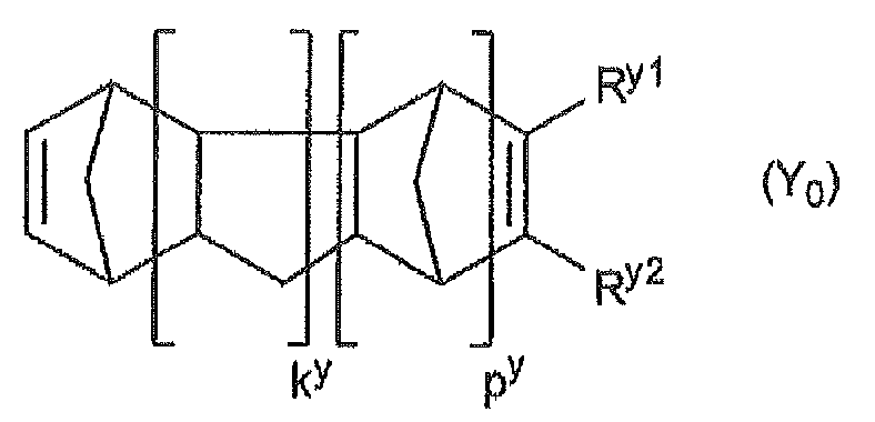
芳香族ポリエーテル系樹脂は、下記式(1)で表される構造単位および下記式(2)で表される構造単位からなる群より選ばれる少なくとも1種の構造単位を有することが好ましい。


ポリイミド系樹脂としては、特に制限されず、繰り返し単位にイミド結合を含む高分子化合物であればよく、例えば、特開2006-199945号公報や特開2008-163107号公報に記載されている方法で合成することができる。
フルオレンポリカーボネート系樹脂としては、特に制限されず、フルオレン部位を含むポリカーボネート樹脂であればよく、例えば、特開2008-163194号公報に記載されている方法で合成することができる。
フルオレンポリエステル系樹脂としては、特に制限されず、フルオレン部位を含むポリエステル樹脂であればよく、例えば、特開2010-285505号公報や特開2011-197450号公報に記載されている方法で合成することができる。
フッ素化芳香族ポリマー系樹脂としては、特に制限されないが、フッ素原子を少なくとも1つ有する芳香族環と、エーテル結合、ケトン結合、スルホン結合、アミド結合、イミド結合およびエステル結合からなる群より選ばれる少なくとも1つの結合を含む繰り返し単位とを含有するポリマーであることが好ましく、例えば特開2008-181121号公報に記載されている方法で合成することができる。
アクリル系紫外線硬化型樹脂としては、特に制限されないが、分子内に一つ以上のアクリル基もしくはメタクリル基を有する化合物と、紫外線によって分解して活性ラジカルを発生させる化合物を含有する樹脂組成物から合成されるものを挙げることができる。アクリル系紫外線硬化型樹脂は、前記基材(i)として、ガラス支持体上やベースとなる樹脂製支持体上に化合物(S)および硬化性樹脂を含む樹脂層(光吸収層)が積層された基材や、化合物(S)を含有する樹脂製基板(ii)上に硬化性樹脂等からなるオーバーコート層などの樹脂層が積層された基材を用いる場合、該硬化性樹脂として特に好適に使用することができる。
ゾルゲル法によるシリカを主成分とする樹脂としては、テトラメトキシシラン、テトラエトキシシラン、ジメトキシジエトキシシラン、メトキシトリエトキシシランなどのテトラアルコキシシラン、フェニルトリメトキシシラン、フェニルトリエトキシシラン、ジフェニルジメトキシシラン、ジフェニルジエトキシシランなどのフェニルアルコキシシラン等から選ばれる1種以上のシラン類の加水分解によるゾルゲル反応により得られる化合物を樹脂として使用することができる。
樹脂の市販品としては、以下の市販品等を挙げることができる。環状ポリオレフィン系樹脂の市販品としては、JSR(株)製アートン、日本ゼオン(株)製ゼオノア、三井化学(株)製APEL、ポリプラスチックス(株)製TOPASなどを挙げることができる。ポリエーテルサルホン系樹脂の市販品としては、住友化学(株)製スミカエクセルPESなどを挙げることができる。ポリイミド系樹脂の市販品としては、三菱ガス化学(株)製ネオプリムLなどを挙げることができる。ポリカーボネート系樹脂の市販品としては、帝人(株)製ピュアエースなどを挙げることができる。フルオレンポリカーボネート系樹脂の市販品としては、三菱ガス化学(株)製ユピゼータEP-5000などを挙げることができる。フルオレンポリエステル系樹脂の市販品としては、大阪ガスケミカル(株)製OKP4HTなどを挙げることができる。アクリル系樹脂の市販品としては、(株)日本触媒製アクリビュアなどを挙げることができる。シルセスキオキサン系紫外線硬化型樹脂の市販品としては、新日鐵化学(株)製シルプラスなどを挙げることができる。
前記基材(i)は、本発明の効果を損なわない範囲において、さらに酸化防止剤、近紫外線吸収剤および蛍光消光剤等の添加剤を含有してもよい。これらその他成分は、1種単独で用いてもよいし、2種以上を併用してもよい。
前記酸化防止剤としては、例えば2,6-ジ-t-ブチル-4-メチルフェノール、2,2'-ジオキシ-3,3'-ジ-t-ブチル-5,5'-ジメチルジフェニルメタン、テトラキス[メチレン-3-(3,5-ジ-t-ブチル-4-ヒドロキシフェニル)プロピオネート]メタン、およびトリス(2,4-ジ-t-ブチルフェニル)ホスファイトなどが挙げられる。
≪樹脂製支持体≫
前記樹脂基板または樹脂製支持体に用いられる樹脂は、前記樹脂層と同様のものを用いることができる。
前記ガラス支持体は、無色透明のガラス基板、CuO含有ガラス基板、またはフツリン酸塩ガラス基板を用いることができる。特に、吸収剤として銅を含むフツリン酸塩ガラス基板は近赤外線カット能を向上させられるため好ましい。
前記基材(i)が、前記樹脂製基板(ii)を含む基材である場合、該樹脂製基板(ii)は、例えば、溶融成形またはキャスト成形により形成することができ、さらに、必要により、成形後に、反射防止剤、ハードコート剤および/または帯電防止剤等のコーティング剤をコーティングすることで、オーバーコート層が積層された基材を製造することができる。
前記溶融成形としては、具体的には、樹脂と化合物(A)等とを溶融混練りして得られたペレットを溶融成形する方法;樹脂と化合物(A)とを含有する樹脂組成物を溶融成形する方法;または、化合物(A)、樹脂および溶剤を含む樹脂組成物から溶剤を除去して得られたペレットを溶融成形する方法などが挙げられる。溶融成形方法としては、射出成形、溶融押出成形またはブロー成形などを挙げることができる。
前記キャスト成形としては、化合物(A)、樹脂および溶剤を含む樹脂組成物を適当な支持体の上にキャスティングして溶剤を除去する方法;または化合物(A)と、光硬化性樹脂および/または熱硬化性樹脂とを含む硬化性組成物を適当な支持体の上にキャスティングして溶媒を除去した後、紫外線照射や加熱などの適切な手法により硬化させる方法などにより製造することもできる。
本発明の光学フィルターは、前記基材(i)の少なくとも一方の面に誘電体多層膜を有する。本発明における誘電体多層膜とは、近赤外線を反射する能力を有する膜または可視域における反射防止効果を有する膜であり、誘電体多層膜を有することでより優れた可視光透過率と近赤外線カット特性を達成することができる。
本発明の光学フィルターは、本発明の効果を損なわない範囲において、基材(i)と誘電体多層膜との間、基材(i)の誘電体多層膜が設けられた面と反対側の面、または誘電体多層膜の基材(i)が設けられた面と反対側の面に、基材(i)や誘電体多層膜の表面硬度の向上、耐薬品性の向上、帯電防止および傷消しなどの目的で、反射防止膜、ハードコート膜や帯電防止膜などの機能膜を適宜設けることができる。
前記機能膜の厚さは、好ましくは0.1~30μm、さらに好ましくは0.5~20μm、特に好ましくは0.7~5μmである。
本発明の光学フィルターは、誘電体多層膜(以下「近赤外線反射層」ともいう。)と、樹脂層(以下「近赤外線吸収層」ともいう。)を含む基材(i)とを有するが、その形態として様々な変形が許容される。
図2(A)は、光入射側から、第1近赤外線反射層118a、近赤外線吸収層120、第2近赤外線反射層118bが設けられた光学フィルター104aを示す。第1近赤外線反射層118aは屈折率の異なる誘電体膜が積層された構造を有する。第2近赤外線反射層118bは、第1近赤外線反射層118aと同じ誘電体多層構造を有していてもよいし、異なる誘電体多層構造を有していてもよい。
図2(B)は、第1近赤外線反射層118aと近赤外線吸収層120との間に第1樹脂層122aが設けられ、第2近赤外線反射層118bと近赤外線吸収層120との間に第2樹脂層122bが設けられた光学フィルター104bを示す。近赤外線反射層と近赤外線吸収層との間に樹脂層を設けることで、光学フィルター104bの薄型化を図りつつ強度を高めることが可能となる。近赤外線吸収層120としては、上述の透光性の樹脂層の中に近赤外線を吸収する化合物を含む層を用いることができる。なお、樹脂層122は、第1樹脂層122a及び第2樹脂層122bの一方のみが設けられていてもよい。また、図2(B)は、近赤外線反射層が近赤外線吸収層の両面に設けられる態様を示すが、光学フィルター104bはこの態様に限定されない。近赤外線反射層は、近赤外線吸収層の片面のみに設けられていてもよい。なお、樹脂層122aおよび122bには近赤外線吸収剤が含まれてもよいし、含まれていなくてもよい。また、第1近赤外線反射層と第2近赤外線反射層のどちらかを反射防止層に代えた構成を用いることもできる。
図3(A)は、透明なガラス基板124を用いて構成される光学フィルター104cを示す。光学フィルター104cは、ガラス基板124の一方の面に近赤外線吸収層120を設け、その上面に第1近赤外線反射層118aが設けられている。近赤外線吸収層120としては、透光性の樹脂層の中に近赤外線を吸収する化合物を含む層が用いられる。また、ガラス基板124の他方の面に第2近赤外線反射層118bが設けられている。透明なガラス基板124は、光学フィルター104の基材(i)の一部(支持体)として用いることができる。ガラス基板124を基材(i)の一部として用いることで、光学フィルター104の剛性を高めることができる。なお、図3(A)において示される第2近赤外線反射層118bを、ガラス基板124と近赤外線吸収層120との間に設けてもよい。
図3(B)は、透明な樹脂基板125を用いて構成される光学フィルター104dを示す。光学フィルター104dは、樹脂基板125の一方の面に近赤外線吸収層120を設け、その上面に第1近赤外線反射層118aが設けられている。また、樹脂基板125の他方の面に第2近赤外線反射層118bが設けられている。樹脂基板125は、光学フィルター104の基材として用いることができる。樹脂基板125を基材として用いることで、光学フィルター104の加工性、柔軟性を高めることができる。なお、図3(B)において示される第2近赤外線反射層118bを、樹脂基板124と近赤外線吸収層120との間に設けてもよい。近赤外線吸収層120としては、透光性の樹脂層の中に近赤外線を吸収する化合物を含む層が用いられる。
近赤外線反射層118は、少なくとも波長400nm~600nmの帯域の可視光線を透過するとともに、少なくとも波長750nm以上の近赤外線を反射するように設計される。近赤外線反射層118は、可視領域の透過率が高く、少なくとも波長400nm~600nmの波長帯域において90%以上の平均分光透過率を有することが好ましい。また、近赤外線反射層118は、波長750nm以上の近赤外線波長帯域においては2%未満の分光透過率を有していることが好ましい。これは、光電変換素子102に近赤外線が入射されず、一方で可視光線帯域の光を高感度で検知するためである。
高屈折率材料層および低屈折率材料層の各層の物理膜厚は、それぞれ層の屈折率にもよるが、通常、5~500nmであることが好ましく、誘電体多層膜の物理膜厚の合計値は光学フィルター全体として1.0~8.0μmであることが好ましい。
化合物(A)等の近赤外線吸収色素を含有する樹脂層の厚みは、「光学フィルター1」および「光学フィルター2」のように、該樹脂層を樹脂基板としての機能を兼ね備えさせる場合は、好ましくは10~300μm、より好ましくは20~200μm、さらに好ましくは25~150μm、特に好ましくは30~120μmである。前記樹脂層の厚みが上記範囲にあると、光学フィルターを軽量化および小型化することができ、光学式指紋認証センサーの低背化を達成することができる。樹脂層の厚みが上記範囲より厚い場合には、光学式指紋認証センサーの低背化という本来の目的が達成できない。一方、前記樹脂層の厚みが上記範囲より薄い場合には、光学フィルターの反りが大きくなる問題がある。
上記樹脂層は、本発明の効果を損なわない範囲において、近赤外線吸収色素の他に酸化防止剤、近紫外線吸収剤、蛍光消光剤および金属錯体系化合物等の添加剤を含有してもよい。また、前述したキャスト成形により基材を製造する場合には、レベリング剤や消泡剤を添加することで基材の製造を容易にすることができる。これら成分は、1種単独で用いてもよいし、2種以上を併用してもよい。
樹脂層を使用する場合には、製造コストや光学特性調整の容易性、さらに、樹脂製基板の耐傷つき性向上等の点から、近赤外線吸収色素を含有する樹脂製基板上に硬化性樹脂からなるオーバーコート層などの樹脂層が積層された基材を用いることが特に好ましい。
前記基材(i)の一部として、銅成分を含む近赤外線吸収ガラス(以下「Cu含有ガラス」ともいう。)を用いることができる。Cu含有ガラスを用いることで、可視光に対する高透過性を有するとともに、近赤外線に対しても高い遮蔽性を有する。なお、リン酸塩ガラスには、ガラス骨格の一部がSiO2で構成されるケイリン酸塩ガラスも含むものとする。Cu含有ガラスとしては、特に国際公開第2017/094672号明細書に記載のCu含有ガラスを好適に用いることができる。
吸収の無いガラス基板としては、主成分として、珪酸塩を含む基板であれば、特に限定されるものではなく、結晶構造を有する石英ガラス基板等が挙げられる。ほかに、ホウ珪酸ガラス基板、ソーダガラス基板および色ガラス基板等を用いることができるが、とりわけ、無アルカリガラス基板、低α線ガラス基板等のガラス基板は、センサー素子への影響が少ないため、好ましい。
本発明において、近赤外線吸収層と近赤外線反射膜の間には樹脂層があってもよい。特に、ガラス基板上に近赤外線吸収層を積層する場合には、前記近赤外線吸収層とガラス基板は、互いに化学的な組成、および熱線膨張率が異なるため、近赤外線吸収層とガラス基板との間に密着層を設けて、それらの十分な密着性を確保することが好ましい。前記密着層は近赤外線吸収層とガラス基板との間の密着性を確保できる材料からなれば、特に限定されないが、例えば、(a)(メタ)アクリロイル基含有化合物に由来する構造単位、(b)カルボン酸基含有化合物に由来する構造単位、および(c)エポキシ基含有化合物に由来する構造単位を有すると、近赤外線吸収層とガラス基板との密着性が高くなるため好ましい。
前記密着層には、本発明の効果を損なわない範囲において、酸発生剤、密着助剤、界面活性剤、重合開始剤等の任意成分を添加することができる。これらの添加量は、所望の特性に応じて適宜選択されるが、前記(メタ)アクリロイル基含有化合物、前記カルボン酸基含有化合物および前記エポキシ基含有化合物の合計100質量部に対して、それぞれ通常0.01~15.0質量部、好ましくは0.05~10.0質量部であることが望ましい。
前記重合開始剤は、紫外線や電子線等の光線に感応してモノマー成分の重合を開始しうる活性種を生じる成分である。このような重合開始剤としては特に限定されるものではないが、O-アシルオキシム化合物、アセトフェノン化合物、ビイミダゾール化合物、アルキルフェノン化合物、ベンゾフェノン化合物などを挙げることができる。これらの具体例としては、エタノン-1-〔9-エチル-6-(2-メチルベンゾイル)-9H-カルバゾール-3-イル〕-1-(O-アセチルオキシム)、1-〔9-エチル-6-ベンゾイル-9.H.-カルバゾール-3-イル〕-オクタン-1-オンオキシム-O-アセテート、1-〔9-エチル-6-(2-メチルベンゾイル)-9.H.-カルバゾール-3-イル〕-エタン-1-オンオキシム-O-ベンゾエート、1-〔9-n-ブチル-6-(2-エチルベンゾイル)-9.H.-カルバゾール-3-イル〕-エタン-1-オンオキシム-O-ベンゾエート、エタノン-1-[9-エチル-6-(2-メチル-4-テトラヒドロフラニルベンゾイル)-9.H.-カルバゾール-3-イル]-1-(O-アセチルオキシム)、1,2-オクタンジオン-1-[4-(フェニルチオ)-2-(O-ベンゾイルオキシム)]、エタノン-1-〔9-エチル-6-(2-メチル-4-テトラヒドロピラニルベンゾイル)-9.H.-カルバゾール-3-イル〕-1-(O-アセチルオキシム)、エタノン-1-〔9-エチル-6-(2-メチル-5-テトラヒドロフラニルベンゾイル)-9.H.-カルバゾール-3-イル〕-1-(O-アセチルオキシム)、エタノン-1-〔9-エチル-6-{2-メチル-4-(2,2-ジメチル-1,3-ジオキソラニル)メトキシベンゾイル}-9.H.-カルバゾール-3-イル〕-1-(O-アセチルオキシム)、2-ベンジル-2-ジメチルアミノ-1-(4-モルホリノフェニル)-ブタン-1-オン、2-ジメチルアミノ-2-(4-メチルベンジル)-1-(4-モルフォリン-4-イル-フェニル)-ブタン-1-オン、2-メチル-1-(4-メチルチオフェニル)-2-モルフォリノプロパン-1-オン、1-フェニル-2-ヒドロキシ-2-メチルプロパン-1-オン、1-(4-i-プロピルフェニル)-2-ヒドロキシ-2-メチルプロパン-1-オン、4-(2-ヒドロキシエトキシ)フェニル-2-ヒドロキシ-2-プロピル)ケトン、1-ヒドロキシシクロヘキシルベンゾフェノン、1-ヒドロキシシクロヘキシルフェニルケトンなどを挙げることができる。これらの重合開始剤は単独で、または2種以上を混合して使用することができる。
密着層の厚みは、本発明の効果を損なわない限り特に制限されないが、好ましくは0.1~5.0μm、さらに好ましくは0.2~3.0μmである。
本発明の光学フィルターは、入射角度が大きい場合においても優れた可視透過率と近赤外線カット能を有する。したがって、光学式指紋認証センサー用として有用である。特に、デジタルスチルカメラ、スマートフォン、タブレット端末、携帯電話、ウェアラブルデバイス、自動車、テレビ、ゲーム機等に搭載される光学式指紋認証センサー用として有用である。
上述した本発明の光学フィルターと、光電変換素子を組み合わせて光学式指紋認証センサーとして用いることができる。ここで、光学式指紋認証センサーとは、指紋画像を取得して個人識別を行うためのセンサーであり、スマートフォンやタブレット、PC等において認証を行うことが可能である。
図1は、本発明の一実施形態に係る光学式指紋認証センサー100aを示す。光学式指紋認証センサー100aは、光学フィルター104及び光電変換素子102を備える。光電変換素子102は、受光部に光が入射すると光起電力効果により電流や電圧を発生する。図1は、一例として、第1電極106、光電変換層108、第2電極114を有する光電変換素子102を示す。光電変換層108は光電効果を発現する半導体で形成される。例えば、光電変換層108は、シリコン半導体を用いて形成される。光学フィルター104は光電変換素子102の受光面側に設けられている。光電変換素子102の受光面には光学フィルター104を通過した光が照射される。
図4は、指紋認証センサー受光素子102aおよび光学フィルター104を備えた光学式指紋認証センサー100aの断面構造の一例を示す。光学式指紋認証センサー100aは、受光素子102aで外光の強度を検知する。受光素子102aの上面には、光学フィルター104が設けられる。光学フィルター104により、受光素子102aの受光面に入射する光から、近赤外線波長領域の光が遮断され、可視光線帯域の光に感応し、より正確な指紋画像を取得できる。
本発明の光学フィルター、他の光学フィルター、レンズ、および光電変換素子等を組み合わせてセンサーモジュールとすることができる。
本発明の電子機器は上述した本発明の光学式指紋認証センサーを含む。以下、図面を参照しながら、本発明の電子機器について説明する。
樹脂の分子量は、各樹脂の溶剤への溶解性等を考慮し、下記の(a)、(b)または(c)の方法にて測定を行った。
t0:溶媒の流下時間
ts:希薄高分子溶液の流下時間
C:0.5g/dL
エスアイアイ・ナノテクノロジーズ株式会社製の示差走査熱量計(DSC6200)を用いて、昇温速度:毎分20℃、窒素気流下で測定した。
ASTM D570に準拠し、試験片を23℃の水中に1週間浸漬させた後、試験片の質量変化より吸水率を測定した。
各種透過率および波長等は、日本分光株式会社製の分光光度計(V-7200)を用いて測定した。
光学フィルターの光学特性(光学フィルターを透過する光の光学特性)と指紋認証センサー、との比較を行い、図4と同様の構成の指紋認証センサーを作成した場合の指紋認証センサー感度特性の評価を行った。評価判断は下記の基準に基づいて行った。
×:入射角度により指紋認証センサーへの入射光の光学特性が変化するため、指紋画像のコントラストが低く、センサー感度特性が低いものであった。
下記実施例および比較例で用いた化合物(A)は、一般的に知られている方法で合成した。一般的合成方法としては、例えば、特許第3366697号公報、特許第2846091号公報、特許第2864475号公報、特許第3703869号公報、特開昭60-228448号公報、特開平1-146846号公報、特開平1-228960号公報、特許第4081149号公報、特開昭63-124054号公報、「フタロシアニン -化学と機能―」(アイピーシー、1997年)、特開2007-169315号公報、特開2009-108267号公報、特開2010-241873号公報、特許第3699464号公報、特許第4740631号公報などに記載されている方法を挙げることができる。
下記式(2)で表される8-メチル-8-メトキシカルボニルテトラシクロ[4.4.0.12,5.17,10]ドデカ-3-エン(以下「DNM」ともいう。)100部と、1-ヘキセン(分子量調節剤)18部と、トルエン(開環重合反応用溶媒)300部とを、窒素置換した反応容器に仕込み、この溶液を80℃に加熱した。次いで、反応容器内の溶液に、重合触媒として、トリエチルアルミニウムのトルエン溶液(0.6mol/リットル)0.2部と、メタノール変性の六塩化タングステンのトルエン溶液(濃度0.025mol/リットル)0.9部とを添加し、この溶液を80℃で3時間加熱攪拌することにより開環重合反応させて開環重合体溶液を得た。この重合反応における重合転化率は97%であった。
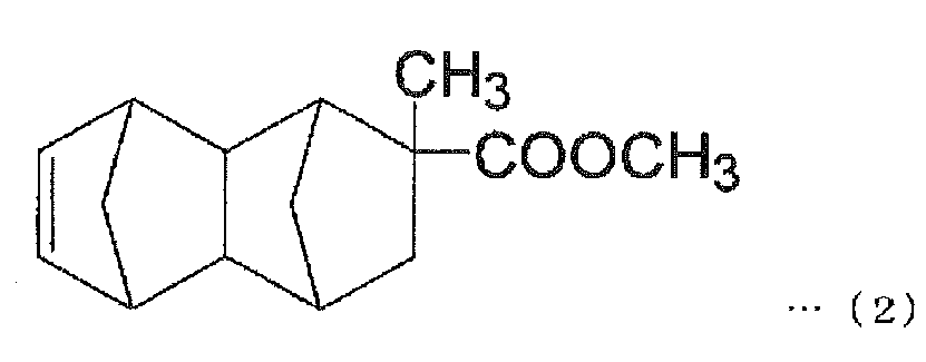
十分に乾燥し、窒素置換した1リットルのステンレス製オートクレーブに、水分6ppmの脱水されたシクロヘキサン;420.4g、p-キシレン;180.2g、5-トリメトキシシリル-ビシクロ[2.2.1]ヘプタ-2-エン;48.75ミリモル(10.43g)、ビシクロ[2.2.1]ヘプタ-2-エン;1,425ミリモル(134.1g)を仕込み、ガス状のエチレンをオートクレーブ内圧が0.1MPaになるように仕込んだ。
温度計、撹拌器、窒素導入管、側管付き滴下ロート、ディーンスターク、冷却管を備えた500mLの5つ口フラスコに、窒素気流下、4,4'-ジアミノジフェニルエーテル 10.0質量部(0.05モル)と、溶剤としてN-メチル-2-ピロリドン 85質量部を仕込んで溶解させた後、1,2,4,5-シクロヘキサンテトラカルボン酸二無水物 11.2質量部(0.05モル)を室温にて固体のまま1時間かけて分割投入し、室温下2時間撹拌した。
3Lの4つ口フラスコに2,6-ジフルオロベンゾニトリル35.12g(0.253mol)、9,9-ビス(4-ヒドロキシフェニル)フルオレン87.60g(0.250mol)、炭酸カリウム41.46g(0.300mol)、N,N-ジメチルアセトアミド(以下「DMAc」ともいう。)443gおよびトルエン111gを添加した。続いて、4つ口フラスコに温度計、撹拌機、窒素導入管付き三方コック、ディーンスターク管および冷却管を取り付けた。次いで、フラスコ内を窒素置換した後、得られた溶液を140℃で3時間反応させ、生成する水をディーンスターク管から随時取り除いた。水の生成が認められなくなったところで、徐々に温度を160℃まで上昇させ、そのままの温度で6時間反応させた。室温(25℃)まで冷却後、生成した塩をろ紙で除去し、ろ液をメタノールに投じて再沈殿させ、ろ別によりろ物(残渣)を単離した。得られたろ物を60℃で一晩真空乾燥し、白色粉末(以下「樹脂D」ともいう。)を得た(収率95%)。得られた樹脂Dは、数平均分子量(Mn)が75,000、重量平均分子量(Mw)が188,000であり、ガラス転移温度(Tg)が285℃であった。
温度計、撹拌器、窒素導入管、側管付き滴下ロート、ディーンスターク管および冷却管を備えた500mLの5つ口フラスコに、窒素気流下、1,4-ビス(4-アミノ-α,α-ジメチルベンジル)ベンゼン27.66g(0.08モル)および4,4'-ビス(4-アミノフェノキシ)ビフェニル7.38g(0.02モル)を入れて、γ―ブチロラクトン68.65g及びN,N-ジメチルアセトアミド17.16gに溶解させた。得られた溶液を、氷水バスを用いて5℃に冷却し、同温に保ちながら1,2,4,5-シクロヘキサンテトラカルボン酸二無水物22.62g(0.1モル)およびイミド化触媒としてトリエチルアミン0.50g(0.005モル)を一括添加した。添加終了後、180℃に昇温し、随時留出液を留去させながら、6時間還流させた。反応終了後、内温が100℃になるまで空冷した後、N,N-ジメチルアセトアミド143.6gを加えて希釈し、攪拌しながら冷却し、固形分濃度20質量%のポリイミド樹脂溶液264.16gを得た。このポリイミド樹脂溶液の一部を1Lのメタノール中に注ぎいれてポリイミドを沈殿させた。濾別したポリイミドをメタノールで洗浄した後、100℃の真空乾燥機中で24時間乾燥させて白色粉末(以下「樹脂E」ともいう。)を得た。得られた樹脂EのIRスペクトルを測定したところ、イミド基に特有の1704cm-1、1770cm-1の吸収が見られた。樹脂Eはガラス転移温度(Tg)が310℃であり、対数粘度を測定したところ、0.87であった。
樹脂合成例1で得た樹脂Aを100質量部に、化合物(A)として、化合物(b-38)(吸収極大波長;710nm)0.1質量部、化合物(a-2)(吸収極大波長;647nm)0.07質量部、および化合物(a-8)(吸収極大波長;685nm)0.10質量部を加え、さらにトルエンを加えて溶解し、固形分が30質量%の溶液を得た。得られた溶液を平滑なガラス板上にキャストし、60℃で8時間、次いで100℃で8時間乾燥した後、ガラス板から剥離した。剥離した樹脂をさらに減圧下100℃で8時間乾燥して、厚さ0.1mm、一辺が60mmの基材を得た。
続いて、得られた基材に、蒸着温度150℃で近赤外線を反射する多層蒸着膜〔シリカ(SiO2)層とチタニア(TiO2)層とが交互に積層されてなるもの〕を表1のような設計で形成し、厚さ0.105mmの光学フィルターを得た。
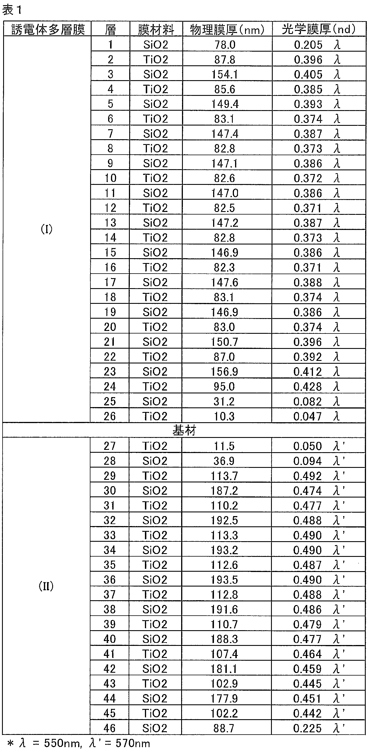
化合物(A)として、化合物(b-37)(吸収極大波長;710nm)0.06質量部および化合物(c-20)(吸収極大波長;685nm)0.07質量部を用いたこと以外は実施例1と同様にして、厚さ0.1mm、一辺が60mmの基材を得て光学特性を評価した。さらに、得られた基材を用いたこと以外は、実施例1と同様にして、厚さ0.105mmの光学フィルターを得て光学特性を評価した。次いで、この光学フィルターを具備した指紋認証センサーの性能評価を実施例1と同様に行った。これらの結果を表3に示す。
化合物(A)として、化合物(b-38)(吸収極大波長;710nm)0.10質量部、化合物(a-22)(吸収極大波長;670nm)0.04質量部および化合物(a-8)(吸収極大波長;685nm)0.02質量部を用いたこと以外は実施例1と同様にして、厚さ0.1mm、一辺が60mmの基材を得て光学特性を評価した。さらに、得られた基材を用いたこと以外は、実施例1と同様にして、厚さ0.105mmの光学フィルターを得て光学特性を評価した。次いで、この光学フィルターを具備した指紋認証センサーの性能評価を実施例1と同様に行った。これらの結果を表3に示す。
樹脂合成例3で得たポリイミド溶液C100質量部に、化合物(A)として、化合物(b-11)0.04質量部および化合物(c-2)0.18質量部を加え、固形分が20質量%の溶液を得た。得られた溶液を平滑なガラス板上にキャストし、60℃で4時間、次いで80℃で4時間乾燥した後、ガラス板から剥離した。剥離した樹脂をさらに減圧下120℃で8時間乾燥して、厚さ0.1mm、一辺が60mmの基材を得た。得られた基材の分光透過率を実施例1と同様に測定し、光学特性を評価した。さらに、得られた基材を用いたこと以外は、実施例1と同様にして、厚さ0.115mmの光学フィルターを得て光学特性を評価した。次いで、この光学フィルターを具備した指紋認証センサーの性能評価を実施例1と同様に行った。これらの結果を表3に示す。
日本ゼオン株式会社製のノルボルネン系樹脂「ゼオノア1400R」(樹脂F)100質量部に、化合物(A)として、化合物(b-39)(吸収極大波長;747nm)0.31質量部および化合物(a-17)0.11質量部を加え、さらにシクロヘキサンとキシレンの7:3混合溶液を加えて溶解し、固形分が20質量%の溶液を得た。得られた溶液を平滑なガラス板上にキャストし、60℃で8時間、次いで80℃で8時間乾燥した後、ガラス板から剥離した。剥離した樹脂をさらに減圧下100℃で24時間乾燥して、厚さ0.1mm、一辺が60mmの基材を得た。得られた基材の分光透過率を実施例1と同様に測定し、光学特性を評価した。さらに、得られた基材を用いたこと以外は、実施例1と同様にして、厚さ0.105mmの近赤外線カットフィルターを得て光学特性を評価した。次いで、この光学フィルターを具備した指紋認証センサーの性能評価を実施例1と同様に行った。これらの結果を表3に示す。
容器に、樹脂合成例1で得られた樹脂A100質量部、化合物(A)として化合物(a-22)(吸収極大波長;670nm)2.00質量部、およびトルエンを加えて樹脂濃度が20質量%の溶液を調製した。得られた溶液を、縦60mm、横60mmの大きさにカットした松浪硝子工業(株)製近赤外線吸収ガラス基板「BS-6」(厚み210μm)上にキャストし、20℃で8時間乾燥した後、さらに減圧下100℃で8時間乾燥して、厚さ0.22mm、縦60mm、横60mmの樹脂層とガラス支持体とからなる基材を得た。得られた基材の分光透過率を実施例1と同様に測定し、光学特性を評価した。さらに、得られた基材を用いたこと以外は、実施例1と同様にして、厚さ0.225mmの光学フィルターを得て光学特性を評価した。次いで、この光学フィルターを具備した指紋認証センサーの性能評価を実施例1と同様に行った。これらの結果を表3に示す。
縦60mm、横60mmの大きさにカットした日本電気硝子(株)製透明ガラス基板「OA-10G」(厚み200um)上に、下記組成の樹脂組成物(H)をバーコーターで塗布し、オーブン中70℃で2分間加熱し、溶剤を揮発除去した。この際、乾燥後の厚みが4μmとなるように、バーコーターの塗布条件を調整した。次に、コンベア式露光機を用いて露光(露光量500mJ/cm2,200mW)を行い、樹脂組成物(H)を硬化させ、ガラス支持体上に樹脂層を形成した。得られた基材の分光透過率を実施例1と同様に測定し、光学特性を評価した。さらに、得られた基材を用いたこと以外は、実施例1と同様にして、厚さ0.109mmの光学フィルターを得て光学特性を評価した。次いで、この光学フィルターを具備した指紋認証センサーの性能評価を実施例1と同様に行った。これらの結果を表3に示す。
日本ゼオン株式会社製のノルボルネン系樹脂「ゼオノア1400R」(樹脂F)100質量部をシクロヘキサンで溶解し、固形分が20質量%の溶液を得た。得られた溶液を平滑なガラス板上にキャストし、60℃で8時間、次いで80℃で8時間乾燥した後、ガラス板から剥離した。剥離した樹脂をさらに減圧下100℃で24時間乾燥して、厚さ0.1mm、一辺が60mmの樹脂製支持体を得た。別容器に、樹脂合成例1で得られた樹脂Aを100質量部、化合物(a-2)0.5質量部、化合物(a-8)1.5質量部、およびトルエンを加えて樹脂濃度が20質量%の溶液を調製した。得られた溶液を上記樹脂製支持体上にキャストし、60℃で8時間、次いで100℃で8時間乾燥して、厚さ0.11mm、一辺が60mmの基材を得た。さらに、得られた基材を用いたこと以外は、実施例1と同様にして、厚さ0.115mmの光学フィルターを得て光学特性を評価した。次いで、この光学フィルターを具備した指紋認証センサーの性能評価を実施例1と同様に行った。これらの結果を表3に示す。
樹脂合成例1で得た樹脂A100質量部に、化合物(b-39)0.09質量部を加え、さらにトルエンを加えて溶解し、固形分が30質量%の溶液を得た。得られた溶液を平滑なガラス板上にキャストし、60℃で8時間、次いで100℃で8時間乾燥した後、ガラス板から剥離した。剥離した樹脂をさらに減圧下100℃で8時間乾燥して、厚さ0.1mm、一辺が60mmの基材を得た。さらに、得られた基材を用いたこと以外は、実施例1と同様にして、厚さ0.115mmの光学フィルターを得て光学特性を評価した。次いで、この光学フィルターを具備した指紋認証センサーの性能評価を実施例1と同様に行った。これらの結果を表3に示す。
化合物(A)を用いなかったこと以外は実施例1と同様にして、厚さ0.1mm、一辺が60mmの基材を得た。さらに、得られた基材を用いたこと以外は、実施例1と同様にして、厚さ0.105mmの光学フィルターを得て光学特性を評価した。次いで、この光学フィルターを具備した指紋認証センサーの性能評価を実施例1と同様に行った。これらの結果を表3に示す。
多層蒸着膜を表3のようにしたこと以外は比較例2と同様にして、厚さ0.106mmの光学フィルターを得て光学特性を評価した。次いで、この光学フィルターを具備した指紋認証センサーの性能評価を実施例1と同様に行った。これらの結果を表3に示す。
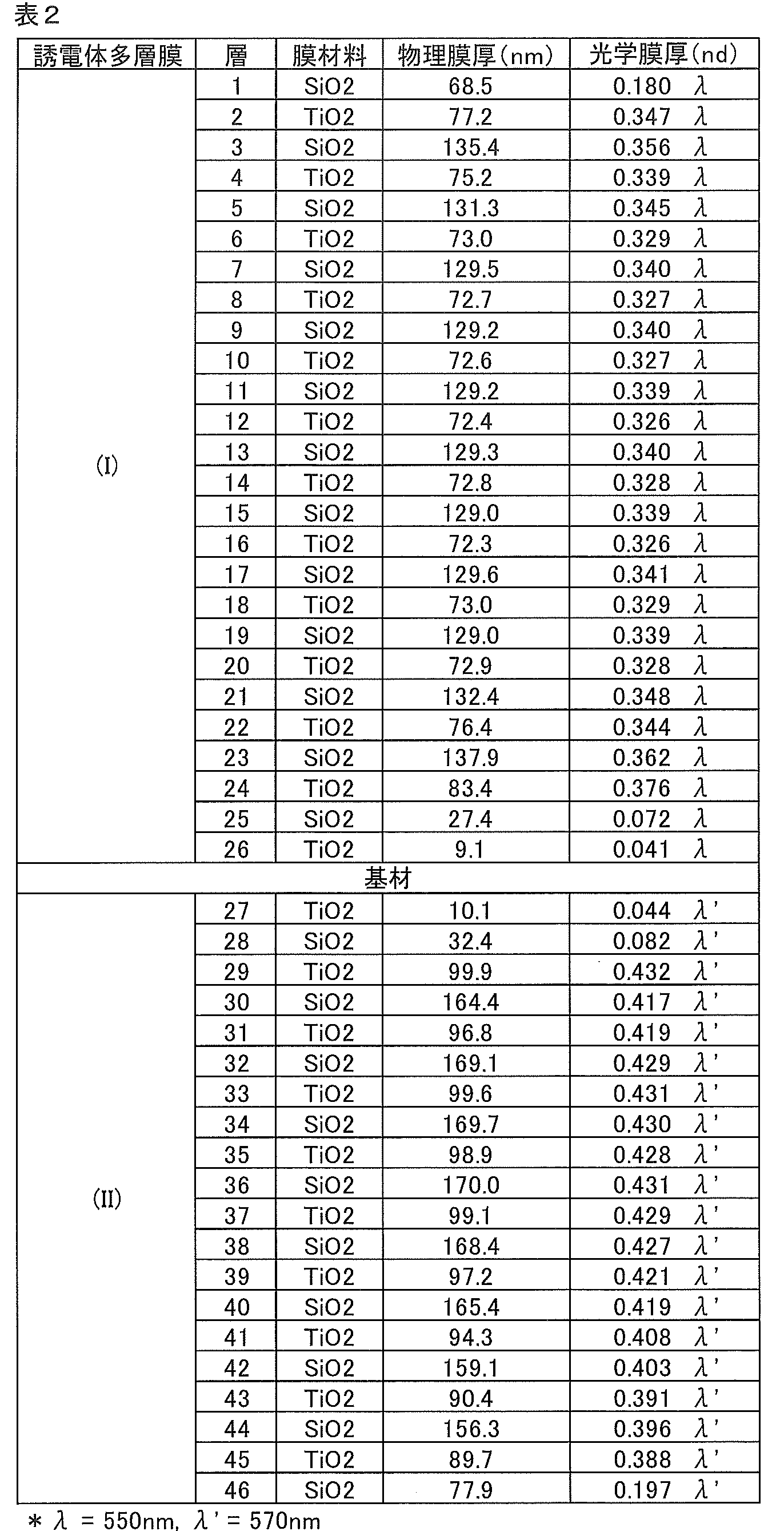

<基材の形態>
形態(1):化合物(A)を含む樹脂製基板
形態(2):樹脂製支持体の片方の面に化合物(A)を含む樹脂層を有する
形態(3):近赤外線吸収ガラス基板の片方の面に化合物(A)を含む樹脂層を有する
形態(4):ガラス基板の片方の面に化合物(A)を含む樹脂層を有する
樹脂A:環状オレフィン系樹脂(樹脂合成例1)
樹脂C:ポリイミド系樹脂(樹脂合成例3)
樹脂F:環状オレフィン系樹脂「ゼオノア 1400R」(日本ゼオン(株)製)
ガラス基板(1):縦60mm、横60mmの大きさにカットした、松浪硝子工業(株)製近赤外線吸収ガラス基板「BS-6」(厚み210μm)
ガラス基板(2):縦60mm、横60mmの大きさにカットした、日本電気硝子(株)製透明ガラス基板「OA-10G」(厚み200μm)
≪化合物(A)≫
化合物(a-2):上記化合物(a-2)(ジクロロメタン中での吸収極大波長647nm)
化合物(a-8):上記化合物(a-8)(ジクロロメタン中での吸収極大波長685nm)
化合物(a-17):上記化合物(a-17)(ジクロロメタン中での吸収極大波長704nm)
化合物(a-22):上記化合物(a-22)(ジクロロメタン中での吸収極大波長670nm)
化合物(b-11):上記化合物(b-11)(ジクロロメタン中での吸収極大波長710nm)
化合物(b-37):上記化合物(b-37)(ジクロロメタン中での吸収極大波長710nm)
化合物(b-38):上記化合物(b-38)(ジクロロメタン中での吸収極大波長710nm)
化合物(b-39):上記化合物(b-39)(ジクロロメタン中での吸収極大波長747nm)
化合物(c-2):上記化合物(c-2)(ジクロロメタン中での吸収極大波長735nm)
化合物(c-20):上記化合物(c-20)(ジクロロメタン中での吸収極大波長685nm)
溶媒(1):トルエン
溶媒(2):N-メチル-2-ピロリドン
溶媒(3):シクロヘキサン/キシレン(質量比:7/3)
3 : 光学フィルター
8 : 分光光度計
9 : ミラー
11 : 光
12 : 光
13 : 光
100:指紋認証センサー
102:光電変換素子
104:光学フィルター
106:第1電極
108:光電変換層
114:第2電極
118:近赤外線反射層
120:近赤外線吸収層
122:樹脂層
124:ガラス基板
125:樹脂基板
132:遮光部材
136:電子機器
138:筐体
140:表示パネル
142:マイクロホン部
144:スピーカ部
145:光学窓
Claims (7)
- 樹脂層を含む基材(i)と、前記基材(i)の少なくとも一方の面に設けられた誘電体多層膜とを有する光学フィルターであって、
波長570~625nmにおいて、前記光学フィルターの面に対して垂直方向から測定した場合の透過率が50%となる最も短い波長を(Ya)nmとし、波長600~1000nmにおいて、前記光学フィルターの前記面に対して垂直方向より5°の角度から測定した場合の反射率が50%となる波長を(Yb)nmとしたとき、(Yb)が{(Ya)+80}nm以上であることを特徴とする光学フィルター。 - 前記基材(i)の吸収極大波長が630~800nmの範囲内にあり、かつ、前記基材(i)の面に対して垂直方向から測定した場合の波長650~670nmにおける平均透過率が20%以下であることを特徴とする請求項1に記載の光学フィルター。
- 光学フィルターの面に対して垂直方向から測定した場合の波長650~1000nmにおける平均透過率が20%以下であることを特徴とする請求項1または2に記載の光学フィルター。
- 光学フィルターの面に対して垂直方向より30°の角度から測定した場合の波長650~670nmにおける平均反射率が20%以下であることを特徴とする請求項1~3のいずれか1項に記載の光学フィルター。
- 前記基材(i)は、波長630~800nmに吸収極大を有する化合物(A)を含有する樹脂製基板(ii)であることを特徴とする請求項1~4のいずれか1項に記載の光学フィルター。
- 前記基材(i)は、ガラス支持体上に、波長630~800nmに吸収極大を有する化合物(A)を含有する樹脂層が積層された基材であることを特徴とする請求項1~4のいずれか1項に記載の光学フィルター。
- 前記基材(i)は、樹脂製支持体上に、波長630~800nmに吸収極大を有する化合物(A)を含有する樹脂層が積層された基材であることを特徴とする請求項1~4のいずれか1項に記載の光学フィルター。
Priority Applications (3)
| Application Number | Priority Date | Filing Date | Title |
|---|---|---|---|
| JP2020541190A JPWO2020050177A1 (ja) | 2018-09-03 | 2019-08-30 | 光学フィルター |
| CN201980052661.XA CN112543881B (zh) | 2018-09-03 | 2019-08-30 | 光学滤波器 |
| KR1020217005611A KR102775397B1 (ko) | 2018-09-03 | 2019-08-30 | 광학 필터 |
Applications Claiming Priority (2)
| Application Number | Priority Date | Filing Date | Title |
|---|---|---|---|
| JP2018-164475 | 2018-09-03 | ||
| JP2018164475 | 2018-09-03 |
Publications (1)
| Publication Number | Publication Date |
|---|---|
| WO2020050177A1 true WO2020050177A1 (ja) | 2020-03-12 |
Family
ID=69722285
Family Applications (1)
| Application Number | Title | Priority Date | Filing Date |
|---|---|---|---|
| PCT/JP2019/034200 Ceased WO2020050177A1 (ja) | 2018-09-03 | 2019-08-30 | 光学フィルター |
Country Status (5)
| Country | Link |
|---|---|
| JP (1) | JPWO2020050177A1 (ja) |
| KR (1) | KR102775397B1 (ja) |
| CN (1) | CN112543881B (ja) |
| TW (1) | TWI813759B (ja) |
| WO (1) | WO2020050177A1 (ja) |
Cited By (4)
| Publication number | Priority date | Publication date | Assignee | Title |
|---|---|---|---|---|
| JP2022026877A (ja) * | 2020-07-31 | 2022-02-10 | 東洋インキScホールディングス株式会社 | 指紋認証センサ用感光性組成物、光学フィルタ、指紋認証センサ、および画像表示装置 |
| JP2022097098A (ja) * | 2020-12-18 | 2022-06-30 | 東洋インキScホールディングス株式会社 | 指紋認証センサ用感光性組成物、光学フィルタ、指紋認証センサ、および画像表示装置 |
| WO2023167062A1 (ja) * | 2022-03-02 | 2023-09-07 | Agc株式会社 | 光学フィルタ |
| CN116835519A (zh) * | 2023-06-29 | 2023-10-03 | 杭州海康微影传感科技有限公司 | 光窗及其制造方法、红外探测器 |
Citations (2)
| Publication number | Priority date | Publication date | Assignee | Title |
|---|---|---|---|---|
| JP2017032685A (ja) * | 2015-07-30 | 2017-02-09 | Jsr株式会社 | 光学フィルターおよび光学フィルターを用いた装置 |
| WO2017094672A1 (ja) * | 2015-11-30 | 2017-06-08 | Jsr株式会社 | 光学フィルター、環境光センサーおよびセンサーモジュール |
Family Cites Families (9)
| Publication number | Priority date | Publication date | Assignee | Title |
|---|---|---|---|---|
| JPH11121841A (ja) * | 1997-10-21 | 1999-04-30 | Canon Inc | レーザー用反射鏡 |
| JP2003233805A (ja) | 2001-12-04 | 2003-08-22 | Canon Inc | 画像入力装置 |
| JP2005018595A (ja) | 2003-06-27 | 2005-01-20 | Canon Inc | 指紋入力装置及びこれを用いた個人認証システム |
| JP2005038406A (ja) | 2003-06-27 | 2005-02-10 | Canon Inc | 指紋入力装置及びこれを用いた個人認証システム |
| JP2005032105A (ja) | 2003-07-09 | 2005-02-03 | Canon Inc | 撮像装置及び指紋認証装置 |
| EP2212726A1 (en) * | 2007-10-30 | 2010-08-04 | 3M Innovative Properties Company | Multi-stack optical bandpass film with electro magnetic interference shielding for optical display filters |
| JP5741283B2 (ja) * | 2010-12-10 | 2015-07-01 | 旭硝子株式会社 | 赤外光透過フィルタ及びこれを用いた撮像装置 |
| US20150192718A1 (en) * | 2012-07-10 | 2015-07-09 | Konica Minolta, Inc. | Infrared shielding film having dielectric multilayer film structure |
| KR102388249B1 (ko) * | 2015-11-27 | 2022-04-20 | 엘지이노텍 주식회사 | 일반 촬영 및 적외선 촬영 겸용 카메라 모듈 |
-
2019
- 2019-08-30 KR KR1020217005611A patent/KR102775397B1/ko active Active
- 2019-08-30 WO PCT/JP2019/034200 patent/WO2020050177A1/ja not_active Ceased
- 2019-08-30 JP JP2020541190A patent/JPWO2020050177A1/ja active Pending
- 2019-08-30 CN CN201980052661.XA patent/CN112543881B/zh active Active
- 2019-09-03 TW TW108131589A patent/TWI813759B/zh active
Patent Citations (2)
| Publication number | Priority date | Publication date | Assignee | Title |
|---|---|---|---|---|
| JP2017032685A (ja) * | 2015-07-30 | 2017-02-09 | Jsr株式会社 | 光学フィルターおよび光学フィルターを用いた装置 |
| WO2017094672A1 (ja) * | 2015-11-30 | 2017-06-08 | Jsr株式会社 | 光学フィルター、環境光センサーおよびセンサーモジュール |
Cited By (7)
| Publication number | Priority date | Publication date | Assignee | Title |
|---|---|---|---|---|
| JP2022026877A (ja) * | 2020-07-31 | 2022-02-10 | 東洋インキScホールディングス株式会社 | 指紋認証センサ用感光性組成物、光学フィルタ、指紋認証センサ、および画像表示装置 |
| JP2022097098A (ja) * | 2020-12-18 | 2022-06-30 | 東洋インキScホールディングス株式会社 | 指紋認証センサ用感光性組成物、光学フィルタ、指紋認証センサ、および画像表示装置 |
| JP7631783B2 (ja) | 2020-12-18 | 2025-02-19 | artience株式会社 | 指紋認証センサ用感光性組成物、光学フィルタ、指紋認証センサ、および画像表示装置 |
| WO2023167062A1 (ja) * | 2022-03-02 | 2023-09-07 | Agc株式会社 | 光学フィルタ |
| JPWO2023167062A1 (ja) * | 2022-03-02 | 2023-09-07 | ||
| JP7856139B2 (ja) | 2022-03-02 | 2026-05-11 | Agc株式会社 | 光学フィルタ |
| CN116835519A (zh) * | 2023-06-29 | 2023-10-03 | 杭州海康微影传感科技有限公司 | 光窗及其制造方法、红外探测器 |
Also Published As
| Publication number | Publication date |
|---|---|
| CN112543881A (zh) | 2021-03-23 |
| CN112543881B (zh) | 2022-12-27 |
| JPWO2020050177A1 (ja) | 2021-08-26 |
| KR102775397B1 (ko) | 2025-03-05 |
| TW202015903A (zh) | 2020-05-01 |
| TWI813759B (zh) | 2023-09-01 |
| KR20210053287A (ko) | 2021-05-11 |
Similar Documents
| Publication | Publication Date | Title |
|---|---|---|
| JP6881660B2 (ja) | 光学フィルターおよび光学センサー装置 | |
| TWI720073B (zh) | 光學濾波器、環境光感測器、感測器模組及電子設備 | |
| KR102434709B1 (ko) | 광학 필터 및 광학 필터를 사용한 장치 | |
| JP6627864B2 (ja) | 光学フィルターおよび光学フィルターを用いた装置 | |
| JP6256335B2 (ja) | 固体撮像素子用光学フィルターおよびその用途 | |
| JP6358114B2 (ja) | 光学フィルターおよび光学フィルターを用いた装置 | |
| KR102384896B1 (ko) | 광학 필터 및 광학 필터를 사용한 장치 | |
| JP6380390B2 (ja) | 光学フィルターおよび前記フィルターを用いた装置 | |
| JP6578718B2 (ja) | 光学フィルターおよび光学フィルターを用いた装置 | |
| CN103858028A (zh) | 滤光器及使用该滤光器的固体摄影装置及照相机模块 | |
| CN112543881B (zh) | 光学滤波器 | |
| JP2017032685A (ja) | 光学フィルターおよび光学フィルターを用いた装置 | |
| WO2014192715A1 (ja) | 光学フィルターおよび前記フィルターを用いた装置 | |
| JP2019124946A (ja) | 光学フィルターおよび光学フィルターを用いた装置 | |
| JP7293875B2 (ja) | 光学フィルターおよび光学センサー装置 | |
| JP2019053157A (ja) | 光学フィルターおよび光学フィルターを用いた装置 | |
| JP2022167805A (ja) | 基材、光学フィルター、固体撮像装置およびカメラモジュール |
Legal Events
| Date | Code | Title | Description |
|---|---|---|---|
| 121 | Ep: the epo has been informed by wipo that ep was designated in this application |
Ref document number: 19856810 Country of ref document: EP Kind code of ref document: A1 |
|
| ENP | Entry into the national phase |
Ref document number: 2020541190 Country of ref document: JP Kind code of ref document: A |
|
| ENP | Entry into the national phase |
Ref document number: 20217005611 Country of ref document: KR Kind code of ref document: A |
|
| NENP | Non-entry into the national phase |
Ref country code: DE |
|
| 122 | Ep: pct application non-entry in european phase |
Ref document number: 19856810 Country of ref document: EP Kind code of ref document: A1 |