WO2020049976A1 - 回路構造体及び電気接続箱 - Google Patents
回路構造体及び電気接続箱 Download PDFInfo
- Publication number
- WO2020049976A1 WO2020049976A1 PCT/JP2019/032097 JP2019032097W WO2020049976A1 WO 2020049976 A1 WO2020049976 A1 WO 2020049976A1 JP 2019032097 W JP2019032097 W JP 2019032097W WO 2020049976 A1 WO2020049976 A1 WO 2020049976A1
- Authority
- WO
- WIPO (PCT)
- Prior art keywords
- terminal
- circuit structure
- conductive
- connection
- semiconductor elements
- Prior art date
- Legal status (The legal status is an assumption and is not a legal conclusion. Google has not performed a legal analysis and makes no representation as to the accuracy of the status listed.)
- Ceased
Links
Images






Classifications
-
- H—ELECTRICITY
- H10—SEMICONDUCTOR DEVICES; ELECTRIC SOLID-STATE DEVICES NOT OTHERWISE PROVIDED FOR
- H10W—GENERIC PACKAGES, INTERCONNECTIONS, CONNECTORS OR OTHER CONSTRUCTIONAL DETAILS OF DEVICES COVERED BY CLASS H10
- H10W40/00—Arrangements for thermal protection or thermal control
- H10W40/10—Arrangements for heating
-
- H—ELECTRICITY
- H01—ELECTRIC ELEMENTS
- H01R—ELECTRICALLY-CONDUCTIVE CONNECTIONS; STRUCTURAL ASSOCIATIONS OF A PLURALITY OF MUTUALLY-INSULATED ELECTRICAL CONNECTING ELEMENTS; COUPLING DEVICES; CURRENT COLLECTORS
- H01R25/00—Coupling parts adapted for simultaneous co-operation with two or more identical counterparts, e.g. for distributing energy to two or more circuits
- H01R25/16—Rails or bus-bars provided with a plurality of discrete connecting locations for counterparts
- H01R25/161—Details
- H01R25/162—Electrical connections between or with rails or bus-bars
-
- H—ELECTRICITY
- H01—ELECTRIC ELEMENTS
- H01R—ELECTRICALLY-CONDUCTIVE CONNECTIONS; STRUCTURAL ASSOCIATIONS OF A PLURALITY OF MUTUALLY-INSULATED ELECTRICAL CONNECTING ELEMENTS; COUPLING DEVICES; CURRENT COLLECTORS
- H01R9/00—Structural associations of a plurality of mutually-insulated electrical connecting elements, e.g. terminal strips or terminal blocks; Terminals or binding posts mounted upon a base or in a case; Bases therefor
- H01R9/22—Bases, e.g. strip, block, panel
- H01R9/24—Terminal blocks
- H01R9/2458—Electrical interconnections between terminal blocks
- H01R9/2466—Electrical interconnections between terminal blocks using a planar conductive structure, e.g. printed circuit board
-
- H—ELECTRICITY
- H02—GENERATION; CONVERSION OR DISTRIBUTION OF ELECTRIC POWER
- H02G—INSTALLATION OF ELECTRIC CABLES OR LINES, OR OF COMBINED OPTICAL AND ELECTRIC CABLES OR LINES
- H02G3/00—Installations of electric cables or lines or protective tubing therefor in or on buildings, equivalent structures or vehicles
- H02G3/02—Details
- H02G3/08—Distribution boxes; Connection or junction boxes
- H02G3/16—Distribution boxes; Connection or junction boxes structurally associated with support for line-connecting terminals within the box
-
- H—ELECTRICITY
- H05—ELECTRIC TECHNIQUES NOT OTHERWISE PROVIDED FOR
- H05K—PRINTED CIRCUITS; CASINGS OR CONSTRUCTIONAL DETAILS OF ELECTRIC APPARATUS; MANUFACTURE OF ASSEMBLAGES OF ELECTRICAL COMPONENTS
- H05K1/00—Printed circuits
- H05K1/02—Details
- H05K1/11—Printed elements for providing electric connections to or between printed circuits
- H05K1/115—Via connections; Lands around holes or via connections
-
- H—ELECTRICITY
- H05—ELECTRIC TECHNIQUES NOT OTHERWISE PROVIDED FOR
- H05K—PRINTED CIRCUITS; CASINGS OR CONSTRUCTIONAL DETAILS OF ELECTRIC APPARATUS; MANUFACTURE OF ASSEMBLAGES OF ELECTRICAL COMPONENTS
- H05K7/00—Constructional details common to different types of electric apparatus
- H05K7/14—Mounting supporting structure in casing or on frame or rack
- H05K7/1422—Printed circuit boards receptacles, e.g. stacked structures, electronic circuit modules or box like frames
- H05K7/1427—Housings
- H05K7/1432—Housings specially adapted for power drive units or power converters
- H05K7/14322—Housings specially adapted for power drive units or power converters wherein the control and power circuits of a power converter are arranged within the same casing
-
- H—ELECTRICITY
- H10—SEMICONDUCTOR DEVICES; ELECTRIC SOLID-STATE DEVICES NOT OTHERWISE PROVIDED FOR
- H10W—GENERIC PACKAGES, INTERCONNECTIONS, CONNECTORS OR OTHER CONSTRUCTIONAL DETAILS OF DEVICES COVERED BY CLASS H10
- H10W70/00—Package substrates; Interposers; Redistribution layers [RDL]
- H10W70/20—Conductive package substrates serving as an interconnection, e.g. metal plates
-
- H—ELECTRICITY
- H10—SEMICONDUCTOR DEVICES; ELECTRIC SOLID-STATE DEVICES NOT OTHERWISE PROVIDED FOR
- H10W—GENERIC PACKAGES, INTERCONNECTIONS, CONNECTORS OR OTHER CONSTRUCTIONAL DETAILS OF DEVICES COVERED BY CLASS H10
- H10W76/00—Containers; Fillings or auxiliary members therefor; Seals
- H10W76/10—Containers or parts thereof
- H10W76/12—Containers or parts thereof characterised by their shape
- H10W76/161—Containers comprising no base
-
- H—ELECTRICITY
- H10—SEMICONDUCTOR DEVICES; ELECTRIC SOLID-STATE DEVICES NOT OTHERWISE PROVIDED FOR
- H10W—GENERIC PACKAGES, INTERCONNECTIONS, CONNECTORS OR OTHER CONSTRUCTIONAL DETAILS OF DEVICES COVERED BY CLASS H10
- H10W90/00—Package configurations
-
- H—ELECTRICITY
- H01—ELECTRIC ELEMENTS
- H01R—ELECTRICALLY-CONDUCTIVE CONNECTIONS; STRUCTURAL ASSOCIATIONS OF A PLURALITY OF MUTUALLY-INSULATED ELECTRICAL CONNECTING ELEMENTS; COUPLING DEVICES; CURRENT COLLECTORS
- H01R2201/00—Connectors or connections adapted for particular applications
- H01R2201/26—Connectors or connections adapted for particular applications for vehicles
-
- H—ELECTRICITY
- H05—ELECTRIC TECHNIQUES NOT OTHERWISE PROVIDED FOR
- H05K—PRINTED CIRCUITS; CASINGS OR CONSTRUCTIONAL DETAILS OF ELECTRIC APPARATUS; MANUFACTURE OF ASSEMBLAGES OF ELECTRICAL COMPONENTS
- H05K2201/00—Indexing scheme relating to printed circuits covered by H05K1/00
- H05K2201/09—Shape and layout
- H05K2201/09209—Shape and layout details of conductors
- H05K2201/09218—Conductive traces
- H05K2201/09236—Parallel layout
-
- H—ELECTRICITY
- H05—ELECTRIC TECHNIQUES NOT OTHERWISE PROVIDED FOR
- H05K—PRINTED CIRCUITS; CASINGS OR CONSTRUCTIONAL DETAILS OF ELECTRIC APPARATUS; MANUFACTURE OF ASSEMBLAGES OF ELECTRICAL COMPONENTS
- H05K2201/00—Indexing scheme relating to printed circuits covered by H05K1/00
- H05K2201/10—Details of components or other objects attached to or integrated in a printed circuit board
- H05K2201/10007—Types of components
- H05K2201/10166—Transistor
-
- H—ELECTRICITY
- H05—ELECTRIC TECHNIQUES NOT OTHERWISE PROVIDED FOR
- H05K—PRINTED CIRCUITS; CASINGS OR CONSTRUCTIONAL DETAILS OF ELECTRIC APPARATUS; MANUFACTURE OF ASSEMBLAGES OF ELECTRICAL COMPONENTS
- H05K2201/00—Indexing scheme relating to printed circuits covered by H05K1/00
- H05K2201/10—Details of components or other objects attached to or integrated in a printed circuit board
- H05K2201/10227—Other objects, e.g. metallic pieces
- H05K2201/10272—Busbars, i.e. thick metal bars mounted on the printed circuit board [PCB] as high-current conductors
-
- H—ELECTRICITY
- H05—ELECTRIC TECHNIQUES NOT OTHERWISE PROVIDED FOR
- H05K—PRINTED CIRCUITS; CASINGS OR CONSTRUCTIONAL DETAILS OF ELECTRIC APPARATUS; MANUFACTURE OF ASSEMBLAGES OF ELECTRICAL COMPONENTS
- H05K2201/00—Indexing scheme relating to printed circuits covered by H05K1/00
- H05K2201/10—Details of components or other objects attached to or integrated in a printed circuit board
- H05K2201/10227—Other objects, e.g. metallic pieces
- H05K2201/10295—Metallic connector elements partly mounted in a hole of the PCB
- H05K2201/10303—Pin-in-hole mounted pins
-
- H—ELECTRICITY
- H05—ELECTRIC TECHNIQUES NOT OTHERWISE PROVIDED FOR
- H05K—PRINTED CIRCUITS; CASINGS OR CONSTRUCTIONAL DETAILS OF ELECTRIC APPARATUS; MANUFACTURE OF ASSEMBLAGES OF ELECTRICAL COMPONENTS
- H05K3/00—Apparatus or processes for manufacturing printed circuits
- H05K3/30—Assembling printed circuits with electric components, e.g. with resistors
- H05K3/32—Assembling printed circuits with electric components, e.g. with resistors electrically connecting electric components or wires to printed circuits
- H05K3/34—Assembling printed circuits with electric components, e.g. with resistors electrically connecting electric components or wires to printed circuits by soldering
- H05K3/3447—Lead-in-hole components
-
- H—ELECTRICITY
- H10—SEMICONDUCTOR DEVICES; ELECTRIC SOLID-STATE DEVICES NOT OTHERWISE PROVIDED FOR
- H10W—GENERIC PACKAGES, INTERCONNECTIONS, CONNECTORS OR OTHER CONSTRUCTIONAL DETAILS OF DEVICES COVERED BY CLASS H10
- H10W70/00—Package substrates; Interposers; Redistribution layers [RDL]
- H10W70/40—Leadframes
- H10W70/479—Leadframes on or in insulating or insulated package substrates, interposers, or redistribution layers
-
- H—ELECTRICITY
- H10—SEMICONDUCTOR DEVICES; ELECTRIC SOLID-STATE DEVICES NOT OTHERWISE PROVIDED FOR
- H10W—GENERIC PACKAGES, INTERCONNECTIONS, CONNECTORS OR OTHER CONSTRUCTIONAL DETAILS OF DEVICES COVERED BY CLASS H10
- H10W70/00—Package substrates; Interposers; Redistribution layers [RDL]
- H10W70/60—Insulating or insulated package substrates; Interposers; Redistribution layers
- H10W70/611—Insulating or insulated package substrates; Interposers; Redistribution layers for connecting multiple chips together
-
- H—ELECTRICITY
- H10—SEMICONDUCTOR DEVICES; ELECTRIC SOLID-STATE DEVICES NOT OTHERWISE PROVIDED FOR
- H10W—GENERIC PACKAGES, INTERCONNECTIONS, CONNECTORS OR OTHER CONSTRUCTIONAL DETAILS OF DEVICES COVERED BY CLASS H10
- H10W70/00—Package substrates; Interposers; Redistribution layers [RDL]
- H10W70/60—Insulating or insulated package substrates; Interposers; Redistribution layers
- H10W70/62—Insulating or insulated package substrates; Interposers; Redistribution layers characterised by their interconnections
- H10W70/65—Shapes or dispositions of interconnections
Definitions
- the present invention relates to a circuit structure on which a semiconductor element is mounted and an electric junction box including the circuit structure.
- an automobile has an electric junction box for distributing electric power from a power supply to loads such as a headlamp and a wiper.
- the electric connection box includes a bus bar connected to a power supply to form a power circuit, and a circuit board having a control circuit for controlling the power circuit.
- the power circuit includes a switching element for supplying / cutting power.
- Patent Document 1 discloses an injection-molded substrate formed by covering a bent circuit conductor with an injection resin. Injection-molded substrates that can be screen printed by flattening have been proposed.
- a circuit structure is a circuit structure in which a plurality of semiconductor elements each including a plurality of first terminals and at least one second terminal provided in parallel with the first terminal are provided.
- a first conductive piece connected to the first terminal of each semiconductor element; a first conductive piece connected to the semiconductor element in a direction in which the semiconductor elements are arranged; one end is connected to the first terminal of each semiconductor element;
- the semiconductor device includes a plurality of connecting portions for connecting the first conductive piece, an insulating portion provided between the connecting portions, and a conductive portion provided on the insulating portion and connected to the second terminal.
- An electric connection box includes the above-described circuit structure, and a control circuit board that controls the semiconductor element of the circuit structure.
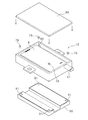
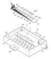
- FIG. 2 is an exploded view of the circuit structure according to the embodiment.
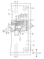
- FIG. 4 is an enlarged view in which a square broken line portion in FIG. 3 is enlarged.
- FIG. 5 is a longitudinal sectional view taken along line VV in FIG. 4.
- FIG. 5 is a vertical sectional view taken along line VI-VI in FIG. 4.
- FIG. 3 is an explanatory diagram illustrating a method for manufacturing a circuit structure according to the embodiment.
- FIG. 3 is an explanatory diagram illustrating a method for manufacturing a circuit structure according to the embodiment.
- FIG. 3 is an explanatory diagram illustrating a method for manufacturing a circuit structure according to the embodiment.
- FIG. 3 is an explanatory diagram illustrating a method for manufacturing a circuit structure according to the embodiment.
- FIG. 3 is an explanatory diagram illustrating a method for manufacturing a circuit structure according to the embodiment.
- FIG. 3 is an explanatory diagram illustrating a method for manufacturing a circuit structure according to the embodiment.
- FIG. 3 is an explanatory diagram illustrating a method for manufacturing a circuit structure according to the embodiment.
- the source terminal and the gate terminal are arranged in a straight line, and the bus bars are respectively arranged at predetermined intervals in accordance with the terminal pitch. Also, the bus bar related to the drain terminal is arranged at a predetermined distance from the bus bar related to the source terminal and the gate terminal.
- a circuit structure includes a circuit structure in which a plurality of semiconductor elements each including a plurality of first terminals and at least one second terminal arranged in parallel with the first terminals are arranged.
- a first conductive piece connected to the first terminal of each semiconductor element; and a first conductive piece connected to the semiconductor element in a direction in which the semiconductor elements are arranged.
- One end is connected to the first terminal of each semiconductor element.
- the first terminal is connected to the connection portion
- the second terminal is connected to the conductive portion provided in the insulating portion provided between the connection portions. Therefore, even when a plurality of semiconductor elements having a small pitch between the first terminal and the second terminal are arranged side by side, wiring can be performed with high accuracy, and the wiring between the first terminal and the second terminal can be provided. The occurrence of a short circuit or the like can be prevented.
- each connection portion is in the shape of a bent rectangular plate, and the insulating portion has a comb-like portion that engages with the one end of each connection portion.
- the insulating portion since the comb-shaped portion of the insulating portion engages with the one end of each joining portion, the insulating portion exists between the connecting portions. Therefore, even when a plurality of semiconductor elements having a small pitch between the first terminal and the second terminal are juxtaposed, wiring can be performed with high accuracy, and the wiring between the wiring of the first terminal and the wiring of the second terminal can be provided. The occurrence of a short circuit or the like can be prevented.
- the first conductive piece and the plurality of connection portions are integrally formed.
- the first conductive piece and the plurality of connecting portions are integrally formed. Therefore, there is no connection point between the first conductive piece and the plurality of connection portions, and the electric resistance between them can be reduced.
- each connection portion may be configured such that an end surface on the one end side connected to the first terminal has a surface and a conductive surface on which the conductive portion is formed in the insulating portion.
- the conductive surface on which the conductive portion is formed in the insulating portion is flush with the end surface on the one end side connected to the first terminal in the connection portion. Therefore, in one semiconductor element, the wiring of the first terminal and the second terminal arranged in parallel can be easily performed.
- the circuit structure according to an aspect of the present disclosure is provided so as to be flush with the conductive surface of the insulating portion, and is separated from the connection portion by a first distance in a direction intersecting a direction in which the connection portions are arranged. And a third terminal of each semiconductor element is connected to the second conductive piece.
- the second conductive piece is arranged at a first distance from the connection portion, and the third terminal is insulated from the first terminal and the second terminal. Further, since the second conductive piece is flush with the conductive surface of the insulating portion, the first terminal, the second terminal, and the third terminal of one semiconductor element are wired on the same surface. be able to.
- the insulating portion is rectangular, and the comb-shaped portion is formed in a portion excluding both ends of one side portion.
- An interval maintaining unit for maintaining the first interval between the first conductive piece and the second conductive piece is provided.
- the gap maintaining section for maintaining the first gap between the first conductive piece and the second conductive piece is provided on the one side of the insulating section where the comb-shaped portion is not formed.
- the semiconductor element is provided at both ends of the portion, that is, at the one side portion where the semiconductor element is not provided. Therefore, it is possible to prevent in advance the problem caused by the expansion of the gap maintaining portion due to the heat generated by the semiconductor element.
- a second portion is provided between the connection portion and the comb-like portion of the insulating portion. An interval is formed.
- the second interval is formed between the connection portion and the comb-shaped portion of the insulating portion in a direction intersecting a direction in which the plurality of connection portions are arranged in parallel. Therefore, for example, when the semiconductor element generates heat, the connecting portions can be deformed in a direction intersecting with the direction in which the plurality of connecting portions are juxtaposed, and the stress can be reduced.
- An electric junction box includes any one of the above-described circuit structures and a control circuit board that controls the semiconductor element of the circuit structure.
- control circuit board controls the semiconductor elements of the circuit structure, and operates the circuit structure as appropriate.
- circuit structure and the electric junction box according to the present embodiment are applied to an electric junction box that distributes power from a power supply to loads such as headlamps and wipers.
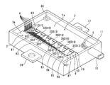
- FIG. 1 is a perspective view showing the appearance of the electric junction box 100 according to the present embodiment
- FIG. 2 is an exploded view of the electric junction box 100 according to the present embodiment.
- the electric connection box 100 according to the present embodiment has a substantially box shape, and includes a control circuit board 9, a circuit structure 10 that accommodates the control circuit board 9, a lid 80 that covers the circuit structure 10,
- a heat sink 90 is provided on the opposite side of the lid 80 with the structure 10 interposed therebetween and radiates heat generated by the circuit structure 10.
- the heat sink 90 is attached to the circuit structure 10 by inserting the screws 70 into the through holes 60 formed at the four corners of the circuit structure 10 and screwing into the screw holes 91 formed at the four corners of the heat sink 90.
- a plurality of semiconductor elements 71 to 77 are arranged in the circuit structure 10 (see FIG. 3).
- the semiconductor elements 71 to 77 are also simply referred to as a semiconductor element 7.
- the semiconductor elements 71 to 77 have the same configuration, for convenience of explanation, the semiconductor element 71 will be described as an example, and the description of the semiconductor elements 72 to 77 will be omitted.
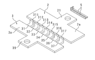
- FIG. 3 is an exploded view of the circuit structure 10 according to the present embodiment
- FIG. 4 is an enlarged view of a square broken line portion in FIG.
- Each semiconductor element 7 is, for example, an FET (more specifically, a surface mount type power MOSFET), and has three source terminals 711 (first terminal), a gate terminal 721 (second terminal), and a drain terminal 731 (FIG. 5). And FIG. 6).
- the three source terminals 711 and the gate terminal 721 are arranged in a straight line, and the drain terminal 731 (third terminal) is provided below the semiconductor element 7.
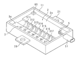
- the semiconductor elements 71 to 77 straddle the first conductive body 3 (integral member) including the first bus bar 3a (first conductive piece) and the second conductive body 2 including the second bus bar 2a (second conductive piece).
- the first conductor 3 and the second conductor 2 are arranged at a predetermined interval 50 (first interval) in a direction (front-back direction) intersecting with the direction in which the semiconductor elements 71 to 77 are arranged.
- One end of each semiconductor element 7 is connected to the first energizer 3, and the other end facing the one end is connected to the second energizer 2.
- the semiconductor elements 71 to 77 are fixed to the second electric conductor 2.
- the first conductive body 3 and the second conductive body 2 are arranged, for example, such that their respective upper surfaces, which are substantially rectangular, are flush with each other. In such a state, the first conductive body 3 and the second conductive body 2 are accommodated in the frame 11.
- the first bus bar 3a of the first conductive body 3 and the second bus bar 2a of the second conductive body 2 are arranged so that their respective longitudinal directions coincide with the longitudinal direction of the frame body 11.
- the frame 11 surrounds and holds the side surfaces of the first and second conductive members 3 and 2.
- the frame 11 is a hollow rectangle and has a predetermined thickness in the vertical direction.
- a connector terminal 5 connected to the control circuit board 9 is provided so as to penetrate the right side wall of the frame 11 in the thickness direction.
- One end protrudes inside the frame 11 and the other end protrudes outside the frame 11. Have been.
- a cylindrical housing 51 that protects the other end of the connector terminal 5 is attached to the outside of the right side wall of the frame 11.
- the first current-carrying member 3 includes the first bus bar 3a, the insulating portion 6, and the connection portions 31 to 37 (connection portions).
- the first conductive body 3 is provided with a terminal plate 39 that rises vertically from the side surface on the front side (long side) of the first bus bar 3a (see FIG. 8).
- the terminal plate 39 is connected to a power supply (battery) or a load (a headlamp, a wiper, or the like).
- the terminal plate 39 penetrates the front side wall of the frame 11 and protrudes outside the frame 11.
- the second energizing body 2 is provided with a terminal plate 21 that rises vertically from the rear (long side) side surface of the second bus bar 2a (see FIG. 8).
- the terminal plate 21 is connected to a power supply (battery) or a load (a headlamp, a wiper, or the like).
- the terminal plate 21 penetrates a rear side wall of the frame 11 and protrudes outside the frame 11.
- FIG. 5 is a longitudinal sectional view taken along line VV in FIG. 4
- FIG. 6 is a longitudinal sectional view taken along line VI-VI in FIG.
- the rear end of the first conductive body 3 and the front end of the second conductive body 2 face each other with an interval 50 therebetween.
- the first conductive body 3 and the second conductive body 2 are insulated.
- the first current-carrying member 3 is provided with an insulating portion 6 in the rear half of the upper surface in the front-rear direction.
- the insulating part 6 is made of a thermoplastic resin having high heat resistance, such as PPS (polyphenylene sulfide).
- the first conductive body 3 is provided with a first bus bar 3a in a front half portion in the front-rear direction.
- the first bus bar 3a is made of, for example, pure copper or a copper alloy, and its upper surface is nickel-plated.
- the insulating portion 6 is substantially rectangular plate-shaped, and is, for example, an insulating substrate. At the rear edge (one side) of the insulating section 6, connection sections 31 to 37 connected to the source terminals of the semiconductor elements 71 to 77 are provided. The connection portions 31 to 37 are respectively connected to three source terminals for each semiconductor element 7. For example, the connection part 31 is connected to three source terminals 711 of the semiconductor element 71 (see FIG. 4).
- the comb portion 600 is formed on the rear edge of the insulating portion 6 except for both ends (see FIG. 9).
- cutout portions 601 to 607 are formed in portions except for both end portions on the rear edge of the insulating portion 6 and corresponding to the connection portions 31 to 37.
- the missing portions 601 to 607 are rectangles following one ends of the connection portions 31 to 37.
- connection portions 31 to 37 are engaged with the comb-shaped portion 600. That is, one ends of the connection portions 31 to 37 are located inside the missing portions 601 to 607, respectively. Thus, the insulating portion 6 exists between the connection portions 31 to 37, and the insulation between the connection portions 31 to 37 is performed.
- connection portions 31 to 37 have, for example, a rectangular plate shape bent in a C shape, and a space 61 is formed inside.
- the connection portions 31 to 37 are arranged along the direction in which the semiconductor elements 71 to 77 are arranged, that is, at equal intervals in the left-right direction.
- One end of each of the connection portions 31 to 37 is connected to the source terminals of the semiconductor elements 71 to 77, and the other end is connected to the first bus bar 3a.
- connection portions 31 to 37 have rectangular end surfaces 311 to 317 on one end side, and the source terminals of the semiconductor elements 71 to 77 are connected to the end surfaces 311 to 317.
- the source terminals of the semiconductor elements 71 to 77 are connected to the end surfaces 311 to 317.
- three source terminals 711 of the semiconductor element 71 are connected to the end face 311 of the connection part 31.
- connection portions 31 to 37 are made of, for example, pure copper or a copper alloy.
- the insulating part 6 is arranged inside the connecting parts 31 to 37 by using, for example, a dowel (not shown) or a positioning part (not shown) provided on the inner side surface of the frame 11.
- a predetermined interval 38 (second interval) is formed between the connection portions 31 to 37 and the comb-shaped portion 600 of the insulating portion 6. More specifically, the connecting portions 31 to 37 are separated from the edges of the cutout portions 601 to 607 of the comb-shaped portion 600 by the second interval 38 in a direction intersecting the direction in which the connecting portions 31 to 37 are arranged, that is, in the front-back direction. ing.
- connection portions 31 to 37 and the first bus bar 3a are integrally formed.
- a plate material of pure copper or a copper alloy is subjected to nickel plating, it is integrally formed by cutting, cutting, pressing, or the like.
- the circuit structure 10 according to the present embodiment there is no so-called connection point in the first current-carrying member 3, and the electric resistance can be reduced.
- the circuit structure 10 according to the present embodiment is not limited to this, and the connection portions 31 to 37 and the first bus bar 3a may be separately provided to form the first conductive body 3.
- the conductive portion 8 is provided in a linear shape on the upper surface 68 of the insulating portion 6.
- the conductive portion 8 is, for example, a copper foil.
- a plurality of pin-shaped connection terminals 4 to be connected to the control circuit board 9 are provided on the left end of the upper surface 68 of the insulating portion 6.
- the conductive portion 8 connects the gate terminal of each semiconductor element 7 to each connection terminal 4. That is, the semiconductor elements 71 to 77 are connected to the connection terminals 4 by the conductive portions 81 to 87, respectively.
- the insulating section 6 may be an insulating substrate, and the conductive sections 81 to 87 may be patterns printed on the upper surface 68 of the insulating section 6.
- each of the conductive portions 81 to 87 may be formed of a groove formed on the upper surface 68 of the insulating portion 6 and a conductive material provided inside the groove so as not to interfere with each other. More specifically, each groove is recessed from a position matching the gate terminal of each of the semiconductor elements 71 to 77 fixed to the second conductor 2 to the corresponding connection terminal 4, and a conductive material such as copper is provided in each groove. Nanoparticle ink may be applied.
- each connection terminal 4 is connected to the gate terminal of each of the semiconductor elements 71 to 77 via the conductive portions 81 to 87.
- the connection terminal 4 is connected to the control circuit board 9, and transmits a control signal transmitted from the control circuit board 9 for controlling the semiconductor elements 71 to 77 to the gates of the semiconductor elements 71 to 77 via the conductive portions 81 to 87. Send to terminal.
- the semiconductor elements 71 to 77 are controlled, and the energization from the first conductive body 3 to the second conductive body 2 or from the second conductive body 2 to the first conductive body 3 is controlled.
- connection portions 31 to 37 are arranged side by side on the rear edge portion (comb-shaped portion 600) in the insulating portion 6, and are arranged in the left-right direction at the edge portion. Are provided in portions excluding both ends.
- the insulating portion 6 has a gap maintaining section 69 for maintaining the gap 50 between the first bus bar 3a and the second bus bar 2a at both ends in the left-right direction at the rear side edge.
- the gap maintaining section 69 has a gap 50 in the lateral direction at the both ends of the insulating section 6 in the left-right direction, toward the second bus bar 2a, in other words, in the direction in which the second conductive body 2 and the first conductive body 3 are separated. Only protruding.
- the present invention is not limited to this, and a configuration may be adopted in which a part of the interval maintaining unit 69 is interposed in the interval 50.
- the gap maintaining portions 69 are provided at both left and right ends of the peripheral portion of the insulating portion 6 apart from the positions of the semiconductor elements 71 to 77. . Therefore, it is possible to prevent a problem caused by the thermal expansion of the gap maintaining portion 69 when the semiconductor elements 71 to 77 generate heat.
- Semiconductor elements 71 to 77 are fixed to the second conductor 2 (second bus bar 2a).
- the second bus bar 2a has a rectangular plate shape, and semiconductor elements 71 to 77 are arranged side by side on the front side on the upper surface. Since the semiconductor elements 71 to 77 have drain terminals below, the semiconductor elements 71 to 77 are fixed to the second bus bar 2a by, for example, soldering the drain terminals to the second bus bar 2a. For example, in the semiconductor element 71, the drain terminal 731 is soldered to the front edge of the second bus bar 2a. Thus, the semiconductor element 71 is connected to the second bus bar 2a and is fixed to the second bus bar 2a.
- a circuit pattern is formed on the control circuit board 9, and a control element such as a microcomputer or a control IC is mounted.
- the control circuit board 9 is connected to the connection terminals 4 and the connector terminals 5.
- the control circuit board 9 transmits a control signal for controlling opening and closing of the semiconductor elements 71 to 77 via the connection terminal 4 and the conductive parts 81 to 87 in response to an instruction signal input via the connector terminal 5. Send to 77.
- the circuit structure 10 according to the present embodiment has a plurality of terminals, and even when a plurality of semiconductor elements 7 having a narrow pitch between terminals are arranged in parallel, the semiconductor element 7 The wiring for each terminal can be performed with high accuracy.
- wiring is performed by the connecting portions 31 to 37 for the source terminal of the semiconductor element 7 and the conductive portion 81 of the insulating portion 6 is connected to the gate terminal.
- the wiring of 87 By performing the wiring of 87, the wiring can be performed with high accuracy, and the occurrence of a short circuit between the wiring of the source terminal and the wiring of the gate terminal can be prevented.
- the conductive portion 8 is provided on the insulating portion 6, and by patterning the conductive portion 8, a large number of wirings can be collectively provided.
- connection portions 31 to 37 are bent in a C shape as described above, and a space 61 is formed inside. Therefore, the one ends of the connection portions 31 to 37 can be vertically deformed. Further, each of the connection portions 31 to 37 has a second space 38 formed between the edges of the cutout portions 601 to 607 of the comb-shaped portion 600 in the left-right direction. An interval 50 is formed between the gap 2a and the gap 2a. Therefore, the one ends of the connection portions 31 to 37 can be deformed in the front-rear direction.
- the semiconductor elements 71 to 77 when the semiconductor elements 71 to 77 generate heat, the semiconductor elements 71 to 77 can be deformed in accordance with the heat generation, and the stress can be reduced. In addition, it is possible to cope with expansion of the second bus bar 2a due to heat generated by the semiconductor elements 71 to 77.
- 7 to 12 are explanatory diagrams illustrating a method for manufacturing the circuit structure 10 according to the present embodiment.
- the surface of a plate made of pure copper or a copper alloy and having a thickness of 2 to 3 mm is subjected to nickel plating, cut into a predetermined shape, and the first and second electric conductors 3 and 2 are formed.
- a bending process is performed on portions to be the connection portions 31 to 37. At this time, the bending process is performed so that the end surfaces 311 to 317 of the connection portions 31 to 37 are flush.
- the first conductive body 3, the second conductive body 2, and the connector terminal 5 are arranged in an insert molding die, and are integrally molded by an injection molding machine.
- a thermoplastic resin having high heat resistance such as PPS (polyphenylene sulfide) is used.
- PPS polyphenylene sulfide
- the insulating portion 6 on which the conductive portion 8 (for example, a wiring pattern) is printed is mounted above the first current-carrying member 3 and inside the connecting portions 31 to 37. Pads for solder mounting are provided on the periphery of the second electric conductor 2, and are arranged in parallel near the end faces 311 to 317 of the connection parts 31 to 37.
- the connection terminal 4 is soldered to the insulating portion 6 in advance.
- solder paste is applied to the second conductor 2 for solder connection of the drain terminal, the end surfaces 311 to 317 of the connection portions 31 to 37 for solder connection of the source terminal, and the mounting pads of the insulating portion 6. Apply 40. Thereafter, the semiconductor elements 71 to 77 are mounted and soldered in a reflow furnace. As a result, the drain terminals of the semiconductor elements 71 to 77 are joined to the second conductor 2, and the source terminals of the semiconductor elements 71 to 77 are joined to the end faces 311 to 317 of the connection portions 31 to 37 of the first conductor 3. . Further, the gate terminals of the connection portions 31 to 37 are joined to the conductive portion 8 of the insulating portion 6.
- connection terminals 4 and the connector terminals 5 are soldered to through-hole portions (see FIG. 3) formed at predetermined positions on the control circuit board 9.
Landscapes
- Engineering & Computer Science (AREA)
- Microelectronics & Electronic Packaging (AREA)
- Architecture (AREA)
- Civil Engineering (AREA)
- Structural Engineering (AREA)
- Connection Or Junction Boxes (AREA)
- Structure Of Printed Boards (AREA)
- Chemical & Material Sciences (AREA)
- Materials Engineering (AREA)
Abstract
複数のソース端子7(11)と、ソース端子(711)と並設された少なくとも一つのゲート端子(721)とを備える半導体素子(71)が複数並設された回路構造体において、各半導体素子(71)のソース端子(711)と接続する第1バスバ(3a)と、半導体素子(71)の並設方向に並設されており、各半導体素子(71)のソース端子(711)に一端が接続され、ソース端子(711)と第1バスバ(3a)とを接続させる複数の接続部(31,32)と、接続部(31,32)同士の間に設けられた絶縁部(6)と、絶縁部(6)に設けられ、ゲート端子(721)と接続された導電部(8)とを備える。
Description
本発明は、半導体素子が実装された回路構造体及び該回路構造体を備える電気接続箱に関する。
本出願は、2018年9月3日出願の日本出願第2018-164663号に基づく優先権を主張し、前記日本出願に記載された全ての記載内容を援用するものである。
本出願は、2018年9月3日出願の日本出願第2018-164663号に基づく優先権を主張し、前記日本出願に記載された全ての記載内容を援用するものである。
従来から、自動車には、電源からヘッドランプ、ワイパー等の負荷へ電力を分配する電気接続箱が搭載されている。電気接続箱は、電源に接続されて電力回路を構成するバスバと、前記電力回路を制御する制御回路を有する回路基板とを備える。電力回路には電力の供給・遮断を行うスイッチング素子等を備える。
特許文献1には、屈曲した回路導体を射出樹脂にて覆って生成される射出成型基板であって、前記回路導体の一部分が射出樹脂から露出され、かつ露出された斯かる一部分が射出樹脂と面一をなすことによって、スクリーン印刷が可能な射出成型基板が提案されている。
本開示の一態様に係る回路構造体は、複数の第1端子と、前記第1端子と並設された少なくとも一つの第2端子とを備える半導体素子が複数並設された回路構造体において、各半導体素子の前記第1端子と接続する第1導電片と、前記半導体素子の並設方向に並設されており、各半導体素子の前記第1端子に一端が接続され、前記第1端子と前記第1導電片とを接続させる複数の接続部と、前記接続部同士の間に設けられた絶縁部と、前記絶縁部に設けられ、前記第2端子と接続された導電部とを備える。
本開示の一態様に係る電気接続箱は、上述した回路構造体と、前記回路構造体の前記半導体素子を制御する制御回路基板とを備える。
[本開示が解決しようとする課題]
一方、MOSFET(Metal Oxide Semiconductor Field Effect Transistor)等の半導体スイッチング素子を用いる場合、ドレイン端子・ソース端子・ゲート端子をそれぞれ別のバスバ上に接続する必要が生じる。
一方、MOSFET(Metal Oxide Semiconductor Field Effect Transistor)等の半導体スイッチング素子を用いる場合、ドレイン端子・ソース端子・ゲート端子をそれぞれ別のバスバ上に接続する必要が生じる。
一般にはスイッチング素子の端子配列は、ソース端子とゲート端子とが直線状に並設され、端子ピッチに合わせて所定間隙にてバスバが夫々配置される。またドレイン端子に係るバスバにおいても、ソース端子・ゲート端子に係るバスバと所定間隙を隔てて配置される。
ところが、近年、スイッチング素子の小型化に伴い、端子ピッチが狭小されつつあり、バスバ同士を隣り合わせる配置が物理的に難しくなっている。また、複数のスイッチング素子を並設させるような場合は、バスバの配置が更に困難である。
しかしながら、特許文献1に係る電子部品搭載用基板においても、このような問題については考慮されておらず、解決することは出来ない。
そこで、狭小な端子ピッチを有する複数の半導体素子を並設する場合において、精度よい配線が可能な回路構造体及び電気接続箱を提供することを目的とする。
[本開示の効果]
本開示の一態様によれば、狭小な端子ピッチを有する複数の半導体素子を並設する場合において、精度よい配線が可能な回路構造体及び電気接続箱を提供できる。
本開示の一態様によれば、狭小な端子ピッチを有する複数の半導体素子を並設する場合において、精度よい配線が可能な回路構造体及び電気接続箱を提供できる。
[本発明の実施形態の説明]
最初に本開示の実施態様を列挙して説明する。また、以下に記載する実施形態の少なくとも一部を任意に組み合わせてもよい。
最初に本開示の実施態様を列挙して説明する。また、以下に記載する実施形態の少なくとも一部を任意に組み合わせてもよい。
(1)本開示の一態様に係る回路構造体は、複数の第1端子と、前記第1端子と並設された少なくとも一つの第2端子とを備える半導体素子が複数並設された回路構造体において、各半導体素子の前記第1端子と接続する第1導電片と、前記半導体素子の並設方向に並設されており、各半導体素子の前記第1端子に一端が接続され、前記第1端子と前記第1導電片とを接続させる複数の接続部と、前記接続部同士の間に設けられた絶縁部と、前記絶縁部に設けられ、前記第2端子と接続された導電部とを備える。
本態様にあっては、前記第1端子を前記接続部に接続させ、前記接続部同士の間に設けられた前記絶縁部内に設けられた前記導電部に前記第2端子を接続させる。従って、前記第1端子及び前記第2端子間のピッチが狭小な複数の半導体素子を並設する場合においても、精度よく配線ができ、前記第1端子の配線及び前記第2端子の配線間にショート等が発生することを防止できる。
(2)本開示の一態様に係る回路構造体は、各接続部は屈曲した矩形板状であり、前記絶縁部は、各接続部の前記一端と係合する櫛歯状部を有する。
本態様にあっては、前記絶縁部の前記櫛歯状部が各接合部の前記一端と係合するので、前記接続部同士の間に前記絶縁部が存在するようになる。従って、前記第1端子及び前記第2端子間のピッチが狭小な複数の半導体素子を並設する場合においても、精度よく配線ができ、前記第1端子の配線及び前記第2端子の配線間にショート等が発生することを防止できる。
(3)本開示の一態様に係る回路構造体は、前記第1導電片及び前記複数の接続部が一体形成されている。
本態様にあっては、前記第1導電片及び前記複数の接続部が一体形成されてある。従って、前記第1導電片及び前記複数の接続部の間における接続点がなくなり、これらの間の電気抵抗を減らすことができる。
(4)本開示の一態様に係る回路構造体は、各接続部は、前記第1端子と接続された前記一端側の端面が、前記絶縁部において前記導電部が形成された導電面と面一である。
本態様にあっては、前記絶縁部において前記導電部が形成された前記導電面と、前記接続部において前記第1端子と接続された前記一端側の端面とは面一である。従って、一つの半導体素子において、並設された前記第1端子及び前記第2端子の配線が容易にできる。
(5)本開示の一態様に係る回路構造体は、前記絶縁部の前記導電面と面一に設けられ、前記接続部の並設方向と交差する方向に、前記接続部と第1間隔離れて配置された第2導電片を備え、各半導体素子の第3端子が前記第2導電片と接続している。
本態様にあっては、前記第2導電片が前記接続部と第1間隔を離れて配置され、前記第3端子と、前記第1端子及び前記第2端子とが絶縁されている。また、前記第2導電片が前記絶縁部の前記導電面と面一であるので、一つの半導体素子が備える前記第1端子、前記第2端子及び前記第3端子を、同一面上に配線することができる。
(6)本開示の一態様に係る回路構造体は、前記絶縁部は、矩形であり、一辺部の両端を除く部分に前記櫛歯状部が形成されており、前記一辺部の両端側に、前記第1導電片及び前記第2導電片の間の前記第1間隔を維持する間隔維持部が設けられている。
本態様にあっては、前記第1導電片及び前記第2導電片の間の前記第1間隔を維持する前記間隔維持部が、前記絶縁部において前記櫛歯状部が形成されていない前記一辺部の両端側、即ち、前記一辺部において前記半導体素子が設けられていないところに設けられている。従って、半導体素子の発熱によって前記間隔維持部が膨張することに起因する問題を事前に防止することができる。
(7)本開示の一態様に係る回路構造体は、前記複数の接続部の並設方向と交差する方向において、前記接続部と前記絶縁部の前記櫛歯状部との間には第2間隔が形成されている。
本態様にあっては、前記接続部と前記絶縁部の前記櫛歯状部との間において、前記複数の接続部の並設方向と交差する方向に、前記第2間隔が形成されている。従って、例えば、半導体素子が発熱した場合、前記複数の接続部の並設方向と交差する方向へ前記接続部が変形することが可能であり、応力を緩和できる。
(8)本開示の一態様に係る電気接続箱は、上述した何れか一つの回路構造体と、前記回路構造体の前記半導体素子を制御する制御回路基板とを備える。
本態様にあっては、前記制御回路基板が前記回路構造体の前記半導体素子を制御し、前記回路構造体を適宜動作させる。
[本発明の実施形態の詳細]
本発明をその実施形態を示す図面に基づいて具体的に説明する。本開示の実施形態に係る回路構造体及び電気接続箱を、以下に図面を参照しつつ説明する。なお、本発明はこれらの例示に限定されるものではなく、請求の範囲によって示され、請求の範囲と均等の意味及び範囲内でのすべての変更が含まれることが意図される。
本発明をその実施形態を示す図面に基づいて具体的に説明する。本開示の実施形態に係る回路構造体及び電気接続箱を、以下に図面を参照しつつ説明する。なお、本発明はこれらの例示に限定されるものではなく、請求の範囲によって示され、請求の範囲と均等の意味及び範囲内でのすべての変更が含まれることが意図される。
以下においては、本実施形態に係る回路構造体及び電気接続箱を、電源からヘッドランプ、ワイパー等の負荷へ電力を分配する電気接続箱に適用した場合を例にあげて説明する。
図1は、本実施形態に係る電気接続箱100の外見を示す斜視図であり、図2は、本実施形態に係る電気接続箱100の分解図である。
本実施形態に係る電気接続箱100は略箱体の形状をなしており、制御回路基板9と、制御回路基板9を収容する回路構造体10と、回路構造体10を覆う蓋80と、回路構造体10を挟んで蓋80と反対側に設けられ、回路構造体10が発する熱を放熱するヒートシンク90とを備える。ヒートシンク90は、ネジ70が回路構造体10の四隅に形成された貫通孔60に挿入されてヒートシンク90の四隅に形成された螺子穴91と螺合することによって回路構造体10に取り付けられる。
本実施形態に係る電気接続箱100は略箱体の形状をなしており、制御回路基板9と、制御回路基板9を収容する回路構造体10と、回路構造体10を覆う蓋80と、回路構造体10を挟んで蓋80と反対側に設けられ、回路構造体10が発する熱を放熱するヒートシンク90とを備える。ヒートシンク90は、ネジ70が回路構造体10の四隅に形成された貫通孔60に挿入されてヒートシンク90の四隅に形成された螺子穴91と螺合することによって回路構造体10に取り付けられる。
回路構造体10には、複数の半導体素子71~77が並設されている(図3参照)。以下、説明の便宜上、半導体素子71~77を単に半導体素子7とも言う。また、半導体素子71~77は同じ構成を有するので、説明の便宜上、半導体素子71の場合を例に挙げて説明し、半導体素子72~77についての説明を省略する。
図3は、本実施形態に係る回路構造体10の分解図であり、図4は、図3の四角の破線部を拡大した拡大図である。
各半導体素子7は、例えばFET(より具体的には面実装タイプのパワーMOSFET)であり、3つのソース端子711(第1端子)、ゲート端子721(第2端子)及びドレイン端子731(図5及び図6参照)を有している。3つのソース端子711とゲート端子721とは直線状に並設されており、ドレイン端子731(第3端子)は半導体素子7の下側に設けられている。
半導体素子71~77は、第1バスバ3a(第1導電片)を備える第1通電体3(一体部材)と、第2バスバ2a(第2導電片)を備える第2通電体2とに跨るように実装されている。即ち、半導体素子71~77の並設方向と交差する方向(前後方向)に、第1通電体3と第2通電体2とが所定の間隔50(第1間隔)隔てて配置されており、各半導体素子7の一端が第1通電体3に接続され、前記一端と対向する他端が第2通電体2に接続されている。半導体素子71~77は第2通電体2に固定されている。
第1通電体3及び第2通電体2は、例えば、略矩形である夫々の上面が面一になるように配置されている。このような状態にて、第1通電体3及び第2通電体2は枠体11内に収容されている。第1通電体3の第1バスバ3a及び第2通電体2の第2バスバ2aは夫々の長手方向が枠体11の長手方向と一致するように配置されている。枠体11は第1通電体3及び第2通電体2の側面を取り囲んで保持している。
枠体11は、中空矩形であり、上下方向に所定の厚みを有する。制御回路基板9と接続されるコネクタ端子5が、枠体11の右側側壁を厚み方向に貫通して設けられ、一端が枠体11の内側に突出され、他端が枠体11の外側に突出されている。枠体11の右側側壁の外側には、コネクタ端子5の他端を保護する円筒形のハウジング51が取り付けられている。
第1通電体3は、第1バスバ3a、絶縁部6及び接続部31~37(接続部)からなる。第1通電体3には、第1バスバ3aの前側(長辺側)の側面から垂直に立ち上がる端子板39が設けられている(図8参照)。端子板39は、電源(バッテリー)又は負荷(ヘッドランプ、ワイパー等)に接続される。端子板39は、枠体11の前側の側壁を貫通し、枠体11の外側に突出している。
第2通電体2には、第2バスバ2aの後側(長辺側)の側面から垂直に立ち上がる端子板21が設けられている(図8参照)。端子板21は、電源(バッテリー)又は負荷(ヘッドランプ、ワイパー等)に接続される。端子板21は、枠体11の後側の側壁を貫通し、枠体11の外側に突出している。
図5は、図4におけるV-V線による縦断面図であり、図6は、図4におけるVI-VI線による縦断面図である。前後方向において、第1通電体3の後側の端部と第2通電体2の前側の端部とは、間隔50を挟んで対向している。これによって、第1通電体3及び第2通電体2は絶縁されている。
第1通電体3は、上面において前後方向の後側半部に絶縁部6が設けられている。絶縁部6は、例えばPPS(ポリフェニレンサルファイド)のような耐熱性の高い熱可塑性樹脂からなる。また、第1通電体3は、前後方向の前側半部に第1バスバ3aが設けられている。第1バスバ3aは、例えば純銅又は銅合金からなり、上面にはニッケルメッキが施されている。
絶縁部6は略矩形板状であり、例えば絶縁基板である。絶縁部6において後側の辺縁(一辺部)には、半導体素子71~77のソース端子と接続される接続部31~37が設けられている。接続部31~37は半導体素子7毎に3つのソース端子と夫々接続する。例えば、接続部31は半導体素子71の3つのソース端子711と接続されている(図4参照)。
より詳しくは、絶縁部6は後側の辺縁において、両端部を除く部分に櫛歯状部600が形成されている(図9参照)。櫛歯状部600では、絶縁部6の後側の辺縁における両端部を除く部分であって接続部31~37に対応する部分に、欠落部601~607が形成されている。欠落部601~607は接続部31~37の一端部に倣う矩形である。
接続部31~37の前記一端部は櫛歯状部600と係合する。即ち、接続部31~37の夫々の一端部は、欠落部601~607の内側に夫々位置する。これによって、接続部31~37同士の間には絶縁部6が存在し、接続部31~37同士間の絶縁が行われる。
接続部31~37は、例えば、C字状に屈曲した矩形板状をなしており、内側には、空間61が形成されている。接続部31~37は、半導体素子71~77の並設方向に沿って、即ち、左右方向に等間隔にて並設されている。接続部31~37は、一端が半導体素子71~77のソース端子と接続され、他端が第1バスバ3aに接続されている。
接続部31~37は一端側の端面311~317が矩形であり、端面311~317に半導体素子71~77のソース端子が接続される。例えば、接続部31の端面311には半導体素子71の3つのソース端子711が接続されている。
また、上述したように、絶縁部6の櫛歯状部600が接続部31~37の前記一端部と係合することによって、接続部31~37同士の間には絶縁部6が設けられている。即ち、接続部31~37の端面311~317同士の間と、接続部31~37の端面311~317及び第1バスバ3aの間とには絶縁部6が設けられている。接続部31~37は、例えば純銅又は銅合金からなる。
絶縁部6は、例えばダボ(図示せず)、又は枠体11の内側面に設けた位置決め部(図示せず)を用いて、接続部31~37の内側に配置されている。後述する導電部8が設けられた絶縁部6の上面68(導電面)と、接続部31~37の前記一端側の端面311~317は面一をなしている(図5参照)。
接続部31~37と、絶縁部6の櫛歯状部600との間には所定の間隔38(第2間隔)が形成されている。詳しくは、各接続部31~37は、接続部31~37の並設方向と交差する方向、即ち前後方向において、櫛歯状部600の欠落部601~607の縁から第2間隔38だけ離れている。
なお、接続部31~37及び第1バスバ3aは一体形成されている。例えば、純銅又は銅合金の板材にニッケルメッキ処理を施した後、切断、切削、プレス加工などにより一体形成される。これによって、本実施形態に係る回路構造体10では、第1通電体3においていわゆる接続点がなくなり、電気抵抗を減らすことができる。
本実施形態に係る回路構造体10はこれに限るものでなく、接続部31~37及び第1バスバ3aを別々に設けて第1通電体3をなしても良い。
本実施形態に係る回路構造体10はこれに限るものでなく、接続部31~37及び第1バスバ3aを別々に設けて第1通電体3をなしても良い。
絶縁部6の上面68には、導電部8が線状に設けられている。導電部8は例えば銅箔である。絶縁部6の上面68において左側の端部には制御回路基板9に接続するピン状の接続端子4が複数突設されている。導電部8は各半導体素子7のゲート端子を各接続端子4に夫々接続させる。
即ち、半導体素子71~77は夫々導電部81~87によって各接続端子4に接続される。例えば、絶縁部6は絶縁基板であり、導電部81~87は絶縁部6の上面68にプリントされたパターンであっても良い。
即ち、半導体素子71~77は夫々導電部81~87によって各接続端子4に接続される。例えば、絶縁部6は絶縁基板であり、導電部81~87は絶縁部6の上面68にプリントされたパターンであっても良い。
本実施形態はこれに限るものでない。例えば、各導電部81~87は、互いに干渉しないように絶縁部6の上面68に形成された溝部と、斯かる溝部の内側に設けられた導電材からなるようにしても良い。
詳しくは、各溝部が、第2通電体2に固定された各半導体素子71~77のゲート端子に整合する位置から夫々対応する接続端子4まで凹設され、各溝部内に導電材、例えば銅ナノ粒子インクを塗布しても良い。
詳しくは、各溝部が、第2通電体2に固定された各半導体素子71~77のゲート端子に整合する位置から夫々対応する接続端子4まで凹設され、各溝部内に導電材、例えば銅ナノ粒子インクを塗布しても良い。
このようにして、各接続端子4は導電部81~87を介して各半導体素子71~77のゲート端子と接続する。
接続端子4は制御回路基板9に接続されており、制御回路基板9が送信する、半導体素子71~77を制御する制御信号を、導電部81~87を介して各半導体素子71~77のゲート端子に送る。これによって、半導体素子71~77が制御され、第1通電体3から第2通電体2へ、又は第2通電体2から第1通電体3への通電が制御される。
接続端子4は制御回路基板9に接続されており、制御回路基板9が送信する、半導体素子71~77を制御する制御信号を、導電部81~87を介して各半導体素子71~77のゲート端子に送る。これによって、半導体素子71~77が制御され、第1通電体3から第2通電体2へ、又は第2通電体2から第1通電体3への通電が制御される。
上述したように、接続部31~37(半導体素子71~77)は、絶縁部6において後側の辺縁部(櫛歯状部600)に並設されており、前記辺縁部において左右方向の両端を除く部分に設けられている。
一方、絶縁部6は、後側の辺縁部における左右方向の両端に、第1バスバ3a及び第2バスバ2aの間の間隔50を維持する間隔維持部69を有している。間隔維持部69は、絶縁部6の前記辺縁部における左右方向の両端部にて、第2バスバ2a側に、換言すれば第2通電体2及び第1通電体3の離隔方向に間隔50だけ突設されている。また、これに限るものでなく、間隔維持部69の一部が間隔50に介在するように構成しても良い。
このように、本実施形態に係る回路構造体10においては、半導体素子71~77の位置から離れて、絶縁部6の前記辺縁部における左右方向の両端部に間隔維持部69を設けている。従って、半導体素子71~77が発熱する際に間隔維持部69が熱膨張することによって生じる問題等を未然に防止出来る。
第2通電体2(第2バスバ2a)には半導体素子71~77が固定されている。第2バスバ2aは矩形の板状であり、上面において、前側の辺縁部に半導体素子71~77が並設されている。半導体素子71~77は下方にドレイン端子を備えているので、ドレイン端子を第2バスバ2aに例えばはんだ付けさせることにより、半導体素子71~77が第2バスバ2aに固定される。
例えば、半導体素子71においては、ドレイン端子731が第2バスバ2aの前側の辺縁部にはんだ付けされている。これによって、半導体素子71が第2バスバ2aに接続されると共に、第2バスバ2aに固定される。
例えば、半導体素子71においては、ドレイン端子731が第2バスバ2aの前側の辺縁部にはんだ付けされている。これによって、半導体素子71が第2バスバ2aに接続されると共に、第2バスバ2aに固定される。
制御回路基板9には、回路パターンが形成されており、マイクロコンピュータ又は制御IC等の制御素子が実装されている。制御回路基板9は接続端子4及びコネクタ端子5に接続されている。制御回路基板9はコネクタ端子5を介して入力される指示信号に応じて、半導体素子71~77の開閉を制御する制御信号を、接続端子4及び導電部81~87を介して半導体素子71~77に送信する。
以上のような構成を有することから、本実施形態に係る回路構造体10は、複数の端子を有し、端子間のピッチが狭小な半導体素子7を複数並設する場合においても、半導体素子7の各端子に係る配線を精度よく行うことができる。
具体的には、本実施形態に係る回路構造体10においては、半導体素子7のソース端子に対しては接続部31~37による配線を行い、ゲート端子に対しては絶縁部6の導電部81~87による配線を行うことにより、配線を精度良く行うことができ、ソース端子の配線とゲート端子の配線間にショートが生じることを防ぐことができる。
更に、導電部8は絶縁部6に設けられており、導電部8をパターン化することによって、多数の配線を集約して設けることができる。
更に、導電部8は絶縁部6に設けられており、導電部8をパターン化することによって、多数の配線を集約して設けることができる。
また、本実施形態に係る回路構造体10と、上述したように、接続部31~37はC字状に屈曲しており、内側には空間61が形成されている。従って、接続部31~37の前記一端部が上下方向に変形することが可能である。
更に、各接続部31~37は、左右方向において、櫛歯状部600の欠落部601~607の縁との間に第2間隔38が形成されており、第2通電体2の第2バスバ2aとの間に間隔50が形成されている。従って、接続部31~37の前記一端部が前後方向に変形することが可能である。
更に、各接続部31~37は、左右方向において、櫛歯状部600の欠落部601~607の縁との間に第2間隔38が形成されており、第2通電体2の第2バスバ2aとの間に間隔50が形成されている。従って、接続部31~37の前記一端部が前後方向に変形することが可能である。
以上のことから、半導体素子71~77が発熱する際、斯かる発熱に応じて変形可能であり、応力を緩和できる。また、半導体素子71~77の発熱による第2バスバ2aの膨張にも対応できる。
以下、本実施形態に係る回路構造体10の製造方法について説明する。図7~図12は、本実施形態に係る回路構造体10の製造方法を説明する説明図である。
先ずは、純銅又は銅合金からなり、厚が2~3mmである板材の表面にニッケルメッキ処理を施し、所定の形状に切断して、第1通電体3及び第2通電体2を成形する。特に、第1通電体3に対しては、櫛型に成形した後、接続部31~37になるべき部分に対して曲げ加工が施される。この際、接続部31~37の端面311~317が面一をなすように曲げ加工が行われる。
第1通電体3、第2通電体2及びコネクタ端子5をインサート成型用金型内に配置して、射出成形機にて一体成型する。成形樹脂には、PPS(ポリフェニレンサルファイド)のような耐熱性の高い熱可塑性樹脂を使用する。これによって、中空矩形の枠体11が成形され、第2通電体2の上面と、接続部31~37の端面311~317が面一をなすよう配設される。
導電部8(例えば、配線パターン)が印刷された絶縁部6を第1通電体3の上側であって、接続部31~37の内側に装着する。
第2通電体2の辺縁部にははんだ実装用パッドが備わり、接続部31~37の端面311~317の近傍に並列される。なお、絶縁部6には、あらかじめ接続端子4をはんだ付けしておく。
第2通電体2の辺縁部にははんだ実装用パッドが備わり、接続部31~37の端面311~317の近傍に並列される。なお、絶縁部6には、あらかじめ接続端子4をはんだ付けしておく。
半導体素子71~77を実装する際、ドレイン端子をはんだ接続する第2通電体2、ソース端子をはんだ接続する接続部31~37の端面311~317、及び絶縁部6の実装用パッドにはんだペースト40を塗布する。この後、半導体素子71~77を載置して、リフロー炉にてはんだ付けを行う。
これによって、半導体素子71~77のドレイン端子が第2通電体2と接合され、半導体素子71~77のソース端子が第1通電体3の接続部31~37の端面311~317に接合される。また、接続部31~37のゲート端子が絶縁部6の導電部8と接合される。
これによって、半導体素子71~77のドレイン端子が第2通電体2と接合され、半導体素子71~77のソース端子が第1通電体3の接続部31~37の端面311~317に接合される。また、接続部31~37のゲート端子が絶縁部6の導電部8と接合される。
次いで、制御回路基板9の所定位置に形成されたスルーホール部(図3参照)に、接続端子4及びコネクタ端子5をはんだ付けする。
今回開示された実施形態はすべての点で例示であって、制限的なものではないと考えられるべきである。本発明の範囲は、上記した意味ではなく、請求の範囲によって示され、請求の範囲と均等の意味及び範囲内でのすべての変更が含まれることが意図される。
2 第2通電体
2a 第2バスバ
3 第1通電体
3a 第1バスバ
4 接続端子
5 コネクタ端子
6 絶縁部
7 半導体素子
8 導電部
9 制御回路基板
10 回路構造体
11 枠体
21 端子板
31~37 接続部
38 第2間隔
39 端子板
50 間隔
51 ハウジング
61 空間
68 上面
69 間隔維持部
71~77 半導体素子
80 蓋
81~87 導電部
100 電気接続箱
311~317 端面
600 櫛歯状部
711 ソース端子
721 ゲート端子
731 ドレイン端子
2a 第2バスバ
3 第1通電体
3a 第1バスバ
4 接続端子
5 コネクタ端子
6 絶縁部
7 半導体素子
8 導電部
9 制御回路基板
10 回路構造体
11 枠体
21 端子板
31~37 接続部
38 第2間隔
39 端子板
50 間隔
51 ハウジング
61 空間
68 上面
69 間隔維持部
71~77 半導体素子
80 蓋
81~87 導電部
100 電気接続箱
311~317 端面
600 櫛歯状部
711 ソース端子
721 ゲート端子
731 ドレイン端子
Claims (8)
- 複数の第1端子と、前記第1端子と並設された少なくとも一つの第2端子とを備える半導体素子が複数並設された回路構造体において、
各半導体素子の前記第1端子と接続する第1導電片と、
前記半導体素子の並設方向に並設されており、各半導体素子の前記第1端子に一端が接続され、前記第1端子と前記第1導電片とを接続させる複数の接続部と、
前記接続部同士の間に設けられた絶縁部と、
前記絶縁部に設けられ、前記第2端子と接続された導電部と
を備える回路構造体。 - 各接続部は屈曲した矩形板状であり、
前記絶縁部は、各接続部の前記一端と係合する櫛歯状部を有する請求項1に記載の回路構造体。 - 前記第1導電片及び前記複数の接続部が一体形成されている請求項2に記載の回路構造体。
- 各接続部は、前記第1端子と接続された前記一端側の端面が、前記絶縁部において前記導電部が形成された導電面と面一である請求項2又は3に記載の回路構造体。
- 前記絶縁部の前記導電面と面一に設けられ、前記接続部の並設方向と交差する方向に、前記接続部と第1間隔離れて配置された第2導電片を備え、
各半導体素子の第3端子が前記第2導電片と接続している請求項4に記載の回路構造体。 - 前記絶縁部は、
矩形であり、
一辺部の両端を除く部分に前記櫛歯状部が形成されており、
前記一辺部の両端側に、前記第1導電片及び前記第2導電片の間の前記第1間隔を維持する間隔維持部が設けられている請求項5に記載の回路構造体。 - 前記複数の接続部の並設方向と交差する方向において、前記接続部と前記絶縁部の前記櫛歯状部との間には第2間隔が形成されている請求項2に記載の回路構造体。
- 請求項1から7の何れか一つに記載の回路構造体と、
前記回路構造体の前記半導体素子を制御する制御回路基板と
を備える電気接続箱。
Priority Applications (2)
| Application Number | Priority Date | Filing Date | Title |
|---|---|---|---|
| US17/271,068 US12027500B2 (en) | 2018-09-03 | 2019-08-16 | Circuit structure and electrical junction box |
| CN201980057297.6A CN112640100B (zh) | 2018-09-03 | 2019-08-16 | 电路结构体及电气连接箱 |
Applications Claiming Priority (2)
| Application Number | Priority Date | Filing Date | Title |
|---|---|---|---|
| JP2018-164663 | 2018-09-03 | ||
| JP2018164663A JP6958515B2 (ja) | 2018-09-03 | 2018-09-03 | 回路構造体及び電気接続箱 |
Publications (1)
| Publication Number | Publication Date |
|---|---|
| WO2020049976A1 true WO2020049976A1 (ja) | 2020-03-12 |
Family
ID=69722480
Family Applications (1)
| Application Number | Title | Priority Date | Filing Date |
|---|---|---|---|
| PCT/JP2019/032097 Ceased WO2020049976A1 (ja) | 2018-09-03 | 2019-08-16 | 回路構造体及び電気接続箱 |
Country Status (4)
| Country | Link |
|---|---|
| US (1) | US12027500B2 (ja) |
| JP (1) | JP6958515B2 (ja) |
| CN (1) | CN112640100B (ja) |
| WO (1) | WO2020049976A1 (ja) |
Citations (3)
| Publication number | Priority date | Publication date | Assignee | Title |
|---|---|---|---|---|
| JP2015138881A (ja) * | 2014-01-22 | 2015-07-30 | 古河電気工業株式会社 | 基板および基板の製造方法 |
| JP2017060256A (ja) * | 2015-09-15 | 2017-03-23 | 株式会社オートネットワーク技術研究所 | 回路構成体および電気接続箱 |
| WO2017104517A1 (ja) * | 2015-12-16 | 2017-06-22 | 株式会社オートネットワーク技術研究所 | 回路構成体、及び電気接続箱 |
Family Cites Families (12)
| Publication number | Priority date | Publication date | Assignee | Title |
|---|---|---|---|---|
| JP2001327044A (ja) * | 2000-05-16 | 2001-11-22 | Auto Network Gijutsu Kenkyusho:Kk | 車両用パワーディストリビュータ |
| JP2004281804A (ja) * | 2003-03-17 | 2004-10-07 | Toyota Motor Corp | 回路基板 |
| JP2007027584A (ja) * | 2005-07-20 | 2007-02-01 | Auto Network Gijutsu Kenkyusho:Kk | 接続構造、回路構成体、およびその製造方法 |
| JP4708941B2 (ja) * | 2005-09-20 | 2011-06-22 | 株式会社オートネットワーク技術研究所 | 接続構造、および回路構成体 |
| US20110205716A1 (en) * | 2008-11-19 | 2011-08-25 | Hiroyuki Moriwaki | Circuit substrate, display panel and display device |
| JP2010199514A (ja) * | 2009-02-27 | 2010-09-09 | Autonetworks Technologies Ltd | 回路構成体 |
| JP5338803B2 (ja) * | 2010-01-22 | 2013-11-13 | 株式会社デンソー | 電力変換装置 |
| JP2014063806A (ja) * | 2012-09-20 | 2014-04-10 | Toshiba Corp | 半導体装置 |
| FR3011346A1 (fr) * | 2013-10-02 | 2015-04-03 | St Microelectronics Sa | Dephaseur electro-optique a capacite d'oxyde |
| JP6115779B2 (ja) * | 2013-11-13 | 2017-04-19 | 株式会社オートネットワーク技術研究所 | スイッチング基板 |
| US20150146340A1 (en) * | 2013-11-26 | 2015-05-28 | Qualcomm Incorporated | Multilayer ceramic capacitor including at least one slot |
| JP6573215B2 (ja) * | 2016-01-27 | 2019-09-11 | 株式会社オートネットワーク技術研究所 | 回路構成体 |
-
2018
- 2018-09-03 JP JP2018164663A patent/JP6958515B2/ja active Active
-
2019
- 2019-08-16 WO PCT/JP2019/032097 patent/WO2020049976A1/ja not_active Ceased
- 2019-08-16 US US17/271,068 patent/US12027500B2/en active Active
- 2019-08-16 CN CN201980057297.6A patent/CN112640100B/zh active Active
Patent Citations (3)
| Publication number | Priority date | Publication date | Assignee | Title |
|---|---|---|---|---|
| JP2015138881A (ja) * | 2014-01-22 | 2015-07-30 | 古河電気工業株式会社 | 基板および基板の製造方法 |
| JP2017060256A (ja) * | 2015-09-15 | 2017-03-23 | 株式会社オートネットワーク技術研究所 | 回路構成体および電気接続箱 |
| WO2017104517A1 (ja) * | 2015-12-16 | 2017-06-22 | 株式会社オートネットワーク技術研究所 | 回路構成体、及び電気接続箱 |
Also Published As
| Publication number | Publication date |
|---|---|
| US12027500B2 (en) | 2024-07-02 |
| CN112640100A (zh) | 2021-04-09 |
| JP6958515B2 (ja) | 2021-11-02 |
| JP2020038882A (ja) | 2020-03-12 |
| CN112640100B (zh) | 2024-10-15 |
| US20210327776A1 (en) | 2021-10-21 |
Similar Documents
| Publication | Publication Date | Title |
|---|---|---|
| US10263405B2 (en) | Circuit assembly and electrical junction box | |
| US10756012B2 (en) | Circuit assembly | |
| US20010045777A1 (en) | Power distributor for vehicle | |
| US10334734B2 (en) | Circuit assembly and electrical junction box | |
| US7736157B2 (en) | Electric connection box | |
| JP7052601B2 (ja) | 回路構成体 | |
| CN112425018B (zh) | 电接线盒 | |
| WO2020049975A1 (ja) | 回路構造体及び回路構造体の製造方法 | |
| JP2017147914A (ja) | 電気接続箱およびワイヤハーネス | |
| JP2011082390A (ja) | 回路構成体および電気接続箱 | |
| US7914297B2 (en) | Electric connection box | |
| CN112640100B (zh) | 电路结构体及电气连接箱 | |
| JP5644223B2 (ja) | 電気接続箱 | |
| US12412877B2 (en) | Circuit assembly and electrical junction box | |
| JP5493800B2 (ja) | 制御装置及び制御装置の製造方法 | |
| US7497698B2 (en) | Electrical module and electrical unit | |
| WO2018173282A1 (ja) | 電気接続箱およびワイヤハーネス | |
| CN109643884B (zh) | 电接线箱 | |
| US12500402B2 (en) | Circuit assembly and electrical junction box | |
| JP4822050B2 (ja) | 回路構成体及びその製造方法 | |
| WO2020017470A1 (ja) | 基板構造体 | |
| JP2006093210A (ja) | 電気回路体 | |
| JP2011101556A (ja) | 電気接続箱及び電気接続箱の製造方法 | |
| WO2018180671A1 (ja) | 回路装置 | |
| JP2004103816A (ja) | 大電流制御ユニットの電子部品実装構造 |
Legal Events
| Date | Code | Title | Description |
|---|---|---|---|
| 121 | Ep: the epo has been informed by wipo that ep was designated in this application |
Ref document number: 19857533 Country of ref document: EP Kind code of ref document: A1 |
|
| NENP | Non-entry into the national phase |
Ref country code: DE |
|
| 122 | Ep: pct application non-entry in european phase |
Ref document number: 19857533 Country of ref document: EP Kind code of ref document: A1 |