WO2020044171A1 - 表示装置 - Google Patents
表示装置 Download PDFInfo
- Publication number
- WO2020044171A1 WO2020044171A1 PCT/IB2019/057030 IB2019057030W WO2020044171A1 WO 2020044171 A1 WO2020044171 A1 WO 2020044171A1 IB 2019057030 W IB2019057030 W IB 2019057030W WO 2020044171 A1 WO2020044171 A1 WO 2020044171A1
- Authority
- WO
- WIPO (PCT)
- Prior art keywords
- protective cover
- display panel
- support
- display device
- angle
- Prior art date
- Legal status (The legal status is an assumption and is not a legal conclusion. Google has not performed a legal analysis and makes no representation as to the accuracy of the status listed.)
- Ceased
Links
Images




Classifications
-
- G—PHYSICS
- G09—EDUCATION; CRYPTOGRAPHY; DISPLAY; ADVERTISING; SEALS
- G09F—DISPLAYING; ADVERTISING; SIGNS; LABELS OR NAME-PLATES; SEALS
- G09F9/00—Indicating arrangements for variable information in which the information is built-up on a support by selection or combination of individual elements
-
- G—PHYSICS
- G06—COMPUTING OR CALCULATING; COUNTING
- G06F—ELECTRIC DIGITAL DATA PROCESSING
- G06F1/00—Details not covered by groups G06F3/00 - G06F13/00 and G06F21/00
- G06F1/16—Constructional details or arrangements
- G06F1/1613—Constructional details or arrangements for portable computers
- G06F1/1633—Constructional details or arrangements of portable computers not specific to the type of enclosures covered by groups G06F1/1615 - G06F1/1626
- G06F1/1637—Details related to the display arrangement, including those related to the mounting of the display in the housing
- G06F1/1652—Details related to the display arrangement, including those related to the mounting of the display in the housing the display being flexible, e.g. mimicking a sheet of paper, or rollable
-
- H—ELECTRICITY
- H10—SEMICONDUCTOR DEVICES; ELECTRIC SOLID-STATE DEVICES NOT OTHERWISE PROVIDED FOR
- H10K—ORGANIC ELECTRIC SOLID-STATE DEVICES
- H10K50/00—Organic light-emitting devices
- H10K50/80—Constructional details
- H10K50/84—Passivation; Containers; Encapsulations
- H10K50/844—Encapsulations
-
- G—PHYSICS
- G02—OPTICS
- G02B—OPTICAL ELEMENTS, SYSTEMS OR APPARATUS
- G02B1/00—Optical elements characterised by the material of which they are made; Optical coatings for optical elements
- G02B1/10—Optical coatings produced by application to, or surface treatment of, optical elements
- G02B1/14—Protective coatings, e.g. hard coatings
-
- G—PHYSICS
- G02—OPTICS
- G02F—OPTICAL DEVICES OR ARRANGEMENTS FOR THE CONTROL OF LIGHT BY MODIFICATION OF THE OPTICAL PROPERTIES OF THE MEDIA OF THE ELEMENTS INVOLVED THEREIN; NON-LINEAR OPTICS; FREQUENCY-CHANGING OF LIGHT; OPTICAL LOGIC ELEMENTS; OPTICAL ANALOGUE/DIGITAL CONVERTERS
- G02F1/00—Devices or arrangements for the control of the intensity, colour, phase, polarisation or direction of light arriving from an independent light source, e.g. switching, gating or modulating; Non-linear optics
- G02F1/01—Devices or arrangements for the control of the intensity, colour, phase, polarisation or direction of light arriving from an independent light source, e.g. switching, gating or modulating; Non-linear optics for the control of the intensity, phase, polarisation or colour
- G02F1/13—Devices or arrangements for the control of the intensity, colour, phase, polarisation or direction of light arriving from an independent light source, e.g. switching, gating or modulating; Non-linear optics for the control of the intensity, phase, polarisation or colour based on liquid crystals, e.g. single liquid crystal display cells
- G02F1/133—Constructional arrangements; Operation of liquid crystal cells; Circuit arrangements
- G02F1/1333—Constructional arrangements; Manufacturing methods
-
- G—PHYSICS
- G02—OPTICS
- G02F—OPTICAL DEVICES OR ARRANGEMENTS FOR THE CONTROL OF LIGHT BY MODIFICATION OF THE OPTICAL PROPERTIES OF THE MEDIA OF THE ELEMENTS INVOLVED THEREIN; NON-LINEAR OPTICS; FREQUENCY-CHANGING OF LIGHT; OPTICAL LOGIC ELEMENTS; OPTICAL ANALOGUE/DIGITAL CONVERTERS
- G02F1/00—Devices or arrangements for the control of the intensity, colour, phase, polarisation or direction of light arriving from an independent light source, e.g. switching, gating or modulating; Non-linear optics
- G02F1/01—Devices or arrangements for the control of the intensity, colour, phase, polarisation or direction of light arriving from an independent light source, e.g. switching, gating or modulating; Non-linear optics for the control of the intensity, phase, polarisation or colour
- G02F1/13—Devices or arrangements for the control of the intensity, colour, phase, polarisation or direction of light arriving from an independent light source, e.g. switching, gating or modulating; Non-linear optics for the control of the intensity, phase, polarisation or colour based on liquid crystals, e.g. single liquid crystal display cells
- G02F1/133—Constructional arrangements; Operation of liquid crystal cells; Circuit arrangements
- G02F1/1333—Constructional arrangements; Manufacturing methods
- G02F1/133305—Flexible substrates, e.g. plastics, organic film
-
- G—PHYSICS
- G02—OPTICS
- G02F—OPTICAL DEVICES OR ARRANGEMENTS FOR THE CONTROL OF LIGHT BY MODIFICATION OF THE OPTICAL PROPERTIES OF THE MEDIA OF THE ELEMENTS INVOLVED THEREIN; NON-LINEAR OPTICS; FREQUENCY-CHANGING OF LIGHT; OPTICAL LOGIC ELEMENTS; OPTICAL ANALOGUE/DIGITAL CONVERTERS
- G02F1/00—Devices or arrangements for the control of the intensity, colour, phase, polarisation or direction of light arriving from an independent light source, e.g. switching, gating or modulating; Non-linear optics
- G02F1/01—Devices or arrangements for the control of the intensity, colour, phase, polarisation or direction of light arriving from an independent light source, e.g. switching, gating or modulating; Non-linear optics for the control of the intensity, phase, polarisation or colour
- G02F1/13—Devices or arrangements for the control of the intensity, colour, phase, polarisation or direction of light arriving from an independent light source, e.g. switching, gating or modulating; Non-linear optics for the control of the intensity, phase, polarisation or colour based on liquid crystals, e.g. single liquid crystal display cells
- G02F1/133—Constructional arrangements; Operation of liquid crystal cells; Circuit arrangements
- G02F1/1333—Constructional arrangements; Manufacturing methods
- G02F1/133308—Support structures for LCD panels, e.g. frames or bezels
-
- G—PHYSICS
- G02—OPTICS
- G02F—OPTICAL DEVICES OR ARRANGEMENTS FOR THE CONTROL OF LIGHT BY MODIFICATION OF THE OPTICAL PROPERTIES OF THE MEDIA OF THE ELEMENTS INVOLVED THEREIN; NON-LINEAR OPTICS; FREQUENCY-CHANGING OF LIGHT; OPTICAL LOGIC ELEMENTS; OPTICAL ANALOGUE/DIGITAL CONVERTERS
- G02F1/00—Devices or arrangements for the control of the intensity, colour, phase, polarisation or direction of light arriving from an independent light source, e.g. switching, gating or modulating; Non-linear optics
- G02F1/01—Devices or arrangements for the control of the intensity, colour, phase, polarisation or direction of light arriving from an independent light source, e.g. switching, gating or modulating; Non-linear optics for the control of the intensity, phase, polarisation or colour
- G02F1/13—Devices or arrangements for the control of the intensity, colour, phase, polarisation or direction of light arriving from an independent light source, e.g. switching, gating or modulating; Non-linear optics for the control of the intensity, phase, polarisation or colour based on liquid crystals, e.g. single liquid crystal display cells
- G02F1/133—Constructional arrangements; Operation of liquid crystal cells; Circuit arrangements
- G02F1/1333—Constructional arrangements; Manufacturing methods
- G02F1/1335—Structural association of cells with optical devices, e.g. polarisers or reflectors
-
- G—PHYSICS
- G02—OPTICS
- G02F—OPTICAL DEVICES OR ARRANGEMENTS FOR THE CONTROL OF LIGHT BY MODIFICATION OF THE OPTICAL PROPERTIES OF THE MEDIA OF THE ELEMENTS INVOLVED THEREIN; NON-LINEAR OPTICS; FREQUENCY-CHANGING OF LIGHT; OPTICAL LOGIC ELEMENTS; OPTICAL ANALOGUE/DIGITAL CONVERTERS
- G02F1/00—Devices or arrangements for the control of the intensity, colour, phase, polarisation or direction of light arriving from an independent light source, e.g. switching, gating or modulating; Non-linear optics
- G02F1/01—Devices or arrangements for the control of the intensity, colour, phase, polarisation or direction of light arriving from an independent light source, e.g. switching, gating or modulating; Non-linear optics for the control of the intensity, phase, polarisation or colour
- G02F1/13—Devices or arrangements for the control of the intensity, colour, phase, polarisation or direction of light arriving from an independent light source, e.g. switching, gating or modulating; Non-linear optics for the control of the intensity, phase, polarisation or colour based on liquid crystals, e.g. single liquid crystal display cells
- G02F1/133—Constructional arrangements; Operation of liquid crystal cells; Circuit arrangements
- G02F1/1333—Constructional arrangements; Manufacturing methods
- G02F1/1335—Structural association of cells with optical devices, e.g. polarisers or reflectors
- G02F1/133528—Polarisers
- G02F1/133541—Circular polarisers
-
- G—PHYSICS
- G06—COMPUTING OR CALCULATING; COUNTING
- G06F—ELECTRIC DIGITAL DATA PROCESSING
- G06F1/00—Details not covered by groups G06F3/00 - G06F13/00 and G06F21/00
- G06F1/16—Constructional details or arrangements
- G06F1/1613—Constructional details or arrangements for portable computers
- G06F1/1615—Constructional details or arrangements for portable computers with several enclosures having relative motions, each enclosure supporting at least one I/O or computing function
- G06F1/1616—Constructional details or arrangements for portable computers with several enclosures having relative motions, each enclosure supporting at least one I/O or computing function with folding flat displays, e.g. laptop computers or notebooks having a clamshell configuration, with body parts pivoting to an open position around an axis parallel to the plane they define in closed position
-
- G—PHYSICS
- G06—COMPUTING OR CALCULATING; COUNTING
- G06F—ELECTRIC DIGITAL DATA PROCESSING
- G06F1/00—Details not covered by groups G06F3/00 - G06F13/00 and G06F21/00
- G06F1/16—Constructional details or arrangements
- G06F1/1613—Constructional details or arrangements for portable computers
- G06F1/1633—Constructional details or arrangements of portable computers not specific to the type of enclosures covered by groups G06F1/1615 - G06F1/1626
- G06F1/1637—Details related to the display arrangement, including those related to the mounting of the display in the housing
- G06F1/1643—Details related to the display arrangement, including those related to the mounting of the display in the housing the display being associated to a digitizer, e.g. laptops that can be used as penpads
-
- G—PHYSICS
- G06—COMPUTING OR CALCULATING; COUNTING
- G06F—ELECTRIC DIGITAL DATA PROCESSING
- G06F3/00—Input arrangements for transferring data to be processed into a form capable of being handled by the computer; Output arrangements for transferring data from processing unit to output unit, e.g. interface arrangements
- G06F3/01—Input arrangements or combined input and output arrangements for interaction between user and computer
- G06F3/03—Arrangements for converting the position or the displacement of a member into a coded form
- G06F3/041—Digitisers, e.g. for touch screens or touch pads, characterised by the transducing means
- G06F3/0412—Digitisers structurally integrated in a display
-
- G—PHYSICS
- G06—COMPUTING OR CALCULATING; COUNTING
- G06F—ELECTRIC DIGITAL DATA PROCESSING
- G06F3/00—Input arrangements for transferring data to be processed into a form capable of being handled by the computer; Output arrangements for transferring data from processing unit to output unit, e.g. interface arrangements
- G06F3/01—Input arrangements or combined input and output arrangements for interaction between user and computer
- G06F3/03—Arrangements for converting the position or the displacement of a member into a coded form
- G06F3/041—Digitisers, e.g. for touch screens or touch pads, characterised by the transducing means
- G06F3/0416—Control or interface arrangements specially adapted for digitisers
- G06F3/04164—Connections between sensors and controllers, e.g. routing lines between electrodes and connection pads
-
- G—PHYSICS
- G09—EDUCATION; CRYPTOGRAPHY; DISPLAY; ADVERTISING; SEALS
- G09F—DISPLAYING; ADVERTISING; SIGNS; LABELS OR NAME-PLATES; SEALS
- G09F9/00—Indicating arrangements for variable information in which the information is built-up on a support by selection or combination of individual elements
- G09F9/30—Indicating arrangements for variable information in which the information is built-up on a support by selection or combination of individual elements in which the desired character or characters are formed by combining individual elements
-
- H—ELECTRICITY
- H05—ELECTRIC TECHNIQUES NOT OTHERWISE PROVIDED FOR
- H05B—ELECTRIC HEATING; ELECTRIC LIGHT SOURCES NOT OTHERWISE PROVIDED FOR; CIRCUIT ARRANGEMENTS FOR ELECTRIC LIGHT SOURCES, IN GENERAL
- H05B33/00—Electroluminescent light sources
- H05B33/02—Details
-
- H—ELECTRICITY
- H05—ELECTRIC TECHNIQUES NOT OTHERWISE PROVIDED FOR
- H05B—ELECTRIC HEATING; ELECTRIC LIGHT SOURCES NOT OTHERWISE PROVIDED FOR; CIRCUIT ARRANGEMENTS FOR ELECTRIC LIGHT SOURCES, IN GENERAL
- H05B33/00—Electroluminescent light sources
- H05B33/12—Light sources with substantially two-dimensional [2D] radiating surfaces
- H05B33/14—Light sources with substantially two-dimensional [2D] radiating surfaces characterised by the chemical or physical composition or the arrangement of the electroluminescent material, or by the simultaneous addition of the electroluminescent material in or onto the light source
-
- H—ELECTRICITY
- H10—SEMICONDUCTOR DEVICES; ELECTRIC SOLID-STATE DEVICES NOT OTHERWISE PROVIDED FOR
- H10K—ORGANIC ELECTRIC SOLID-STATE DEVICES
- H10K50/00—Organic light-emitting devices
- H10K50/80—Constructional details
- H10K50/86—Arrangements for improving contrast, e.g. preventing reflection of ambient light
-
- H—ELECTRICITY
- H10—SEMICONDUCTOR DEVICES; ELECTRIC SOLID-STATE DEVICES NOT OTHERWISE PROVIDED FOR
- H10K—ORGANIC ELECTRIC SOLID-STATE DEVICES
- H10K59/00—Integrated devices, or assemblies of multiple devices, comprising at least one organic light-emitting element covered by group H10K50/00
- H10K59/10—OLED displays
-
- H—ELECTRICITY
- H10—SEMICONDUCTOR DEVICES; ELECTRIC SOLID-STATE DEVICES NOT OTHERWISE PROVIDED FOR
- H10K—ORGANIC ELECTRIC SOLID-STATE DEVICES
- H10K59/00—Integrated devices, or assemblies of multiple devices, comprising at least one organic light-emitting element covered by group H10K50/00
- H10K59/40—OLEDs integrated with touch screens
-
- H—ELECTRICITY
- H10—SEMICONDUCTOR DEVICES; ELECTRIC SOLID-STATE DEVICES NOT OTHERWISE PROVIDED FOR
- H10K—ORGANIC ELECTRIC SOLID-STATE DEVICES
- H10K59/00—Integrated devices, or assemblies of multiple devices, comprising at least one organic light-emitting element covered by group H10K50/00
- H10K59/80—Constructional details
- H10K59/87—Passivation; Containers; Encapsulations
-
- H—ELECTRICITY
- H10—SEMICONDUCTOR DEVICES; ELECTRIC SOLID-STATE DEVICES NOT OTHERWISE PROVIDED FOR
- H10K—ORGANIC ELECTRIC SOLID-STATE DEVICES
- H10K59/00—Integrated devices, or assemblies of multiple devices, comprising at least one organic light-emitting element covered by group H10K50/00
- H10K59/80—Constructional details
- H10K59/8791—Arrangements for improving contrast, e.g. preventing reflection of ambient light
-
- H—ELECTRICITY
- H10—SEMICONDUCTOR DEVICES; ELECTRIC SOLID-STATE DEVICES NOT OTHERWISE PROVIDED FOR
- H10K—ORGANIC ELECTRIC SOLID-STATE DEVICES
- H10K77/00—Constructional details of devices covered by this subclass and not covered by groups H10K10/80, H10K30/80, H10K50/80 or H10K59/80
- H10K77/10—Substrates, e.g. flexible substrates
-
- H—ELECTRICITY
- H10—SEMICONDUCTOR DEVICES; ELECTRIC SOLID-STATE DEVICES NOT OTHERWISE PROVIDED FOR
- H10K—ORGANIC ELECTRIC SOLID-STATE DEVICES
- H10K77/00—Constructional details of devices covered by this subclass and not covered by groups H10K10/80, H10K30/80, H10K50/80 or H10K59/80
- H10K77/10—Substrates, e.g. flexible substrates
- H10K77/111—Flexible substrates
-
- G—PHYSICS
- G06—COMPUTING OR CALCULATING; COUNTING
- G06F—ELECTRIC DIGITAL DATA PROCESSING
- G06F2203/00—Indexing scheme relating to G06F3/00 - G06F3/048
- G06F2203/041—Indexing scheme relating to G06F3/041 - G06F3/045
- G06F2203/04102—Flexible digitiser, i.e. constructional details for allowing the whole digitising part of a device to be flexed or rolled like a sheet of paper
-
- G—PHYSICS
- G06—COMPUTING OR CALCULATING; COUNTING
- G06F—ELECTRIC DIGITAL DATA PROCESSING
- G06F2203/00—Indexing scheme relating to G06F3/00 - G06F3/048
- G06F2203/041—Indexing scheme relating to G06F3/041 - G06F3/045
- G06F2203/04103—Manufacturing, i.e. details related to manufacturing processes specially suited for touch sensitive devices
-
- G—PHYSICS
- G09—EDUCATION; CRYPTOGRAPHY; DISPLAY; ADVERTISING; SEALS
- G09F—DISPLAYING; ADVERTISING; SIGNS; LABELS OR NAME-PLATES; SEALS
- G09F9/00—Indicating arrangements for variable information in which the information is built-up on a support by selection or combination of individual elements
- G09F9/30—Indicating arrangements for variable information in which the information is built-up on a support by selection or combination of individual elements in which the desired character or characters are formed by combining individual elements
- G09F9/301—Indicating arrangements for variable information in which the information is built-up on a support by selection or combination of individual elements in which the desired character or characters are formed by combining individual elements flexible foldable or roll-able electronic displays, e.g. thin LCD, OLED
-
- Y—GENERAL TAGGING OF NEW TECHNOLOGICAL DEVELOPMENTS; GENERAL TAGGING OF CROSS-SECTIONAL TECHNOLOGIES SPANNING OVER SEVERAL SECTIONS OF THE IPC; TECHNICAL SUBJECTS COVERED BY FORMER USPC CROSS-REFERENCE ART COLLECTIONS [XRACs] AND DIGESTS
- Y02—TECHNOLOGIES OR APPLICATIONS FOR MITIGATION OR ADAPTATION AGAINST CLIMATE CHANGE
- Y02E—REDUCTION OF GREENHOUSE GAS [GHG] EMISSIONS, RELATED TO ENERGY GENERATION, TRANSMISSION OR DISTRIBUTION
- Y02E10/00—Energy generation through renewable energy sources
- Y02E10/50—Photovoltaic [PV] energy
- Y02E10/549—Organic PV cells
Definitions
- One embodiment of the present invention relates to a display device.
- the present invention relates to a display device having a flexible display.
- the technical field of one embodiment of the present invention disclosed in this specification and the like includes a semiconductor device, a display device, a light-emitting device, a power storage device, a storage device, an electronic device, a lighting device, an input device, an input / output device, and a driving method thereof. Or a method for producing the same, as an example.
- a semiconductor device generally refers to a device that can function by utilizing semiconductor characteristics.
- a display element used for a flexible display a light-emitting element such as an organic EL (Electro Luminescence) element or a liquid crystal element is typically given.
- organic EL Electro Luminescence
- the basic structure of the organic EL element is such that a layer containing a light-emitting organic compound is sandwiched between a pair of electrodes. By applying a voltage to this element, light emission can be obtained from a light-emitting organic compound. Since a display device to which such an organic EL element is applied does not require a light source such as a backlight, a thin, lightweight, high-contrast display device with low power consumption can be realized.
- Patent Document 1 discloses a flexible light emitting device to which an organic EL element is applied.
- the flexible display is extremely thin compared to the conventional display, there is a problem that it is difficult to increase the mechanical strength. Particularly when the flexible display functions as a touch panel, if the finger or a stylus strongly touches the display surface, the flexible display may be damaged.
- One object of one embodiment of the present invention is to prevent breakage of a flexible display. Another object is to provide a display device with increased mechanical strength. Another object is to provide a highly reliable display device. Another object is to provide a display device or an electronic device having a novel structure.
- One embodiment of the present invention is a display device including a display panel and a protective cover.
- the display panel has a first portion having flexibility.
- the protective cover has translucency and flexibility, and is provided on the display surface side of the display panel so as to overlap.
- the display device has a function of reversibly transforming into a first mode and a second mode.
- the first mode the display panel and the protective cover are each substantially flat.
- the second mode the first portion of the display panel is curved such that the display surface side is a concave curved surface, and a part of the protective cover is curved in the same direction as the first portion.
- a gap is provided between the first portion and the protective cover.
- the display panel and the protective cover are provided in contact with each other.
- the display panel and the protective cover are provided separately from each other.
- the protective cover preferably has a function as a touch panel or a circularly polarizing plate.
- a functional layer having flexibility is provided between the display panel and the protective cover. At this time, in the second mode, it is preferable that a part of the functional layer bends in the same direction as the first part. Further, the functional layer preferably has a function as a touch panel or a circularly polarizing plate.
- the display panel has a second portion and a third portion, and the first portion is located between the second portion and the third portion;
- the second portion and the third portion are substantially flat, and the portion of the protective cover overlapping the second portion and the third portion have a substantially flat region. Is preferred.
- the angle formed by the surface of the second portion and the surface of the third portion is an angle ⁇
- the angle ⁇ is set to 180 degrees in a range of 90 degrees or more and less than 180 degrees.
- the curvature of the first portion is within a range of 90 degrees or more and less than 180 degrees.
- the radius has an angle range smaller than the radius of curvature of the curved portion of the protective cover, and in the range where the angle ⁇ is equal to or more than 0 degree and less than 90 degrees, the radius of curvature of the first portion is equal to the radius of curvature of the curved portion of the protective cover.
- the angle formed by the surface of the second portion and the surface of the third portion is an angle ⁇
- the angle ⁇ is set to 180 degrees in a range of 90 degrees or more and less than 180 degrees. It is preferable to have an angle range in which the distance between the first portion and the protective cover is gradually increased when the distance is gradually reduced.
- the protective cover when the angle formed by the surface of the second portion and the surface of the third portion is an angle ⁇ , the protective cover has a bending direction in a range of 90 ° to 180 °. Preferably, tension is applied in a direction perpendicular to the pair of intersecting ends.
- first support fixed to the second portion and a second support fixed to the third portion.
- first portion is not fixed to either the first support or the second support.
- one of a pair of ends of the protective cover that intersects the bending direction is fixed to the first support, and the other is used as both the first support and the second support. Preferably, it is not fixed.
- the first support has a first rotation axis perpendicular to the bending direction of the second portion, and the second support has a second rotation axis parallel to the first rotation axis. It is preferable to have a rotation axis of At this time, the first support and the second support are rotatable in opposite directions around the first rotation axis or the second rotation axis and at the same angle, respectively. It is preferable that the relative position to the second rotation axis does not change.
- the first support and the second support each have a holding member, and the protective cover is slidably attached to the holding member.
- the protective cover preferably contains at least one of a urethane resin, an acrylic resin, and a silicone resin.
- breakage of a flexible display can be prevented.
- a display device with increased mechanical strength can be provided.
- a highly reliable display device can be provided.
- a display device or an electronic device having a novel structure can be provided.
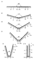
- 1A to 1E are diagrams illustrating a configuration example of a display device.
- 2A to 2F are diagrams illustrating a configuration example of a display device.
- 3A to 3F are diagrams illustrating a configuration example of a display device.
- 4A to 4D are diagrams illustrating a configuration example of a display device.
- 5A to 5F are diagrams illustrating a configuration example of a display device.
- 6A to 6F are diagrams illustrating a configuration example of a display device.
- 7A to 7D are diagrams illustrating a configuration example of a display device.
- 8A to 8C are diagrams illustrating a configuration example of a display device.
- 9A to 9D are diagrams illustrating a configuration example of a display device.
- FIG. 10A to 10F2 are diagrams illustrating a configuration example of a display device.
- FIG. 11 is a diagram illustrating a configuration example of a display device.
- 12A and 12B are diagrams illustrating a configuration example of a display device.
- FIG. 13 is a diagram illustrating a configuration example of a display panel.
- FIG. 14 is a diagram illustrating a configuration example of a display panel.
- FIG. 15 is a diagram illustrating a configuration example of a display panel.
- FIG. 16A is a block diagram of a display device.
- 16B and 16C are circuit diagrams of pixels.
- 17A, 17C, and 17D are circuit diagrams of the display device.
- FIG. 17B is a timing chart.
- 18A to 18E are diagrams illustrating a configuration example of a pixel.
- a display panel which is one embodiment of a display device has a function of displaying (outputting) an image or the like on a display surface. Therefore, the display panel is one mode of an output device.
- a display panel substrate to which a connector such as FPC (Flexible Printed Circuit) or TCP (Tape Carrier Package) is attached, or an IC by COG (Chip On Glass) method or the like is attached to the substrate.
- a connector such as FPC (Flexible Printed Circuit) or TCP (Tape Carrier Package) is attached, or an IC by COG (Chip On Glass) method or the like is attached to the substrate.
- a display panel module a display module, or simply a display panel.
- a touch panel which is one embodiment of a display device has a function of displaying an image or the like on a display surface and a function of detecting, pressing, or approaching a detection target such as a finger or a stylus on the display surface. And a function as a touch sensor for detection. Therefore, a touch panel is one mode of an input / output device.
- the touch panel can also be called, for example, a display panel with a touch sensor (or a display device) or a display panel with a touch sensor function (or a display device).
- the touch panel may have a configuration including a display panel and a touch sensor panel.
- a structure having a function as a touch sensor can be provided inside or on the surface of the display panel.
- a device in which a connector or an IC is mounted on a substrate of a touch panel is sometimes referred to as a touch panel module, a display module, or simply a touch panel.
- FIG. 1A is a schematic perspective view of the display device 10.
- the display device 10 includes a display panel 11, a protective cover 12, a support 21, and a support 22.
- the display panel 11 has a display unit 15.
- At least a part of the display panel 11 has flexibility and can be curved.
- a plurality of pixels are arranged in a matrix on the display section 15 of the display panel 11, and an image can be displayed on the display section 15.
- At least one or more display elements are provided for the pixels provided in the display unit 15 of the display panel 11.
- a display element an organic EL element can be typically used.
- various display elements such as a light-emitting element such as an inorganic EL element and an LED element, a liquid crystal element, a microcapsule, an electrophoresis element, an electrowetting element, an electrofluidic element, an electrochromic element, and a MEMS element can be used. it can.
- the protective cover 12 is located on the display surface side of the display panel 11 and has a function of protecting the surface of the display panel 11.
- the protective cover 12 has a light-transmitting property, and a user can see an image displayed on the display unit 15 through the protective cover 12. Further, at least a part of the protective cover 12 has flexibility and can be curved.
- the protective cover 12 may have a function as a touch sensor panel or a function as an optical film.
- the protective cover 12 may be configured to include a sensor element such as a capacitive touch sensor, an optical sensor, or a pressure-sensitive touch sensor.
- the optical film include a circularly polarizing plate and an anti-reflection film (including an AR (Anti-Reflection) film and an AG (Anti-Glare) film).
- urethane resin As the protective cover 12, a sheet-shaped member having at least one of urethane resin, acrylic resin, silicone resin, fluorine resin, olefin resin, vinyl resin, styrene resin, amide resin, ester resin, and epoxy resin is used. Is preferred.
- urethane resin has a relatively high dielectric constant, and can increase sensitivity when a capacitance type touch sensor is applied.
- the surface of the protective cover 12 can be provided with a function of high slipperiness and self-healing properties, which is preferable.
- an organic resin having a self-healing property as a material located on the outermost surface of the protective cover 12 because surface scattering due to scratches or the like can be prevented and display quality can be maintained.
- a water-repellent or oil-repellent resin as the organic resin, or by performing a surface treatment for imparting water repellency or oil repellency, stains such as fingerprint marks adhere to the surface of the protective cover 12. Can be prevented.
- the material having self-healing properties for example, a material containing polyrotaxane, cyclodextrin, polyphenylene ether, or the like can be used in addition to the urethane resin described above.
- the protective cover 12 has a configuration in which the organic resin having the self-healing property is laminated on a sheet made of at least one of the urethane resin, the acrylic resin, and the silicone resin described above.
- the protective cover 12 in order to improve the lubricity of the outermost surface of the protective cover 12, it is preferable to perform coating, surface treatment, or to apply a film having high lubricity. In addition, by improving the slipperiness not only on the display surface side of the protective cover 12 but also on the display panel 11 side, when the display panel 11 and the protective cover 12 are provided in contact with each other, they become slippery. preferable.
- the support 21 and the support 22 have a function of supporting the display panel 11. It is preferable that at least the surface of the support 21 and the support 22 that supports the display panel 11 be a flat surface or a smooth curved surface. Further, it is preferable that the surface has such a rigidity that the surface does not deform even when pressed by a finger or a stylus. For example, it is preferable to use a relatively rigid material such as plastic, glass, metal, alloy, ceramic, or wood for the surfaces of the support 21 and the support 22 that support the display panel 11.
- the display panel 11 has a portion fixed to the support 21, a portion fixed to the support 22, and a portion not fixed to any support between these two portions. It is preferable that at least a portion of the display panel 11 that is not fixed to the support 21 and the support 22 has flexibility.
- FIG. 1B is a schematic perspective view of the display device 10 in a state where the display panel 11 and the protective cover 12 are not curved.
- the display panel 11 is in a state of being supported by either the support 21 or the support 22. Further, a protective cover 12 is provided on the display surface side of the display panel 11. In this state, since the entire display panel 11 is supported by the rigid supports 21 and 22, the display panel 11 has high mechanical strength against pressure from the display surface side. At this time, the support 21 and the support 22 may be in close contact with each other at least between the respective surfaces supporting the display panel 11 (also referred to as seams) so that a gap or a step is not generated as much as possible. preferable.
- FIG. 1C is a schematic perspective view of the display device 10 in a state where the display panel 11 and the protective cover 12 are curved.
- the display panel 11 is curved such that a part on the display surface side has a concave curved surface.
- the protective cover 12 is also curved in the same direction so that a part on the display surface side is concave.
- 1D and 1E are enlarged views of regions P and Q in FIG. 1C, respectively.
- the direction D of the arrow indicated by the broken line in FIGS. 1B and 1C corresponds to the bending direction of the display panel 11.
- the case where the display panel 11 is curved so that the long side direction of the display panel 11 matches the bending direction is shown.
- the bending direction is not limited to this, and may match the short side direction. Further, the direction may not be parallel to any of the sides forming the outline of the display panel 11.
- the region P is a region including the ends of the curved portions of the display panel 11 and the protective cover 12.
- the region Q is a region including the ends of the non-curved portions of the display panel 11 and the protective cover 12.
- the display panel 11 and the protective cover 12 are separated from each other in the curved portions of the display panel 11 and the protective cover 12, respectively. That is, it can be said that there is a gap between the curved portion of the display panel 11 and the protective cover 12.
- an end also referred to as a side
- the protective cover 12 is deformed so as to be shifted outward relative to the end of the support 22.
- FIGS. 1A to 1E the display panel 11 and the protective cover 12 are not bent when the display panel 11 and the protective cover 12 are viewed from the top, so that the state of the shift is easily understood.
- the respective ends of the cover 12, the support 21, and the support 22 are shown to coincide.
- the protective cover 12 When the display panel 11 is curved, the protective cover 12 is deformed so as to be relatively displaced with respect to the display panel 11, so that both the display panel 11 and the protective cover 12 are not expanded and contracted in the curved portion. A gap can be provided between the panel 11 and the protective cover 12.
- FIG. 2A is a cross-sectional view along the bending direction when the display panel 11 and the protective cover 12 are in close contact with each other
- FIG. 2B is a cross-sectional view when a crescent-shaped gap is provided therebetween.
- the display panel 11 even if the display panel 11 is not curved and is protruded from the protective cover 12 side by a tapered member (a stylus 29 in this case) at a portion supported by the support body 22, Since the pressure can be absorbed by the deformation of the protective cover 12, the display panel 11 can be prevented from being deformed and damaged. On the other hand, in the curved portion of the display panel 11, since the back side of the display panel 11 is not supported, the display panel 11 is also deformed following the deformation of the protective cover 12. As a result, in the worst case, the display panel 11 may be damaged and the stylus 29 may penetrate.
- a tapered member a stylus 29 in this case
- the case where the curved portion of the display panel 11 is not supported by the support 21 and the support 22 has been described.
- a support that can also support the curved portion of the display panel 11. at least the surface supporting the display panel 11 needs to be deformed or stretched. Therefore, the surface of the support that supports the display panel 11 needs to have flexibility or elasticity, and it is difficult to achieve high rigidity. Therefore, when the display panel 11 is protruded from the display surface side, the surface of the support is deformed by the pressure, and the display panel 11 itself may be deformed into a concave shape and may be damaged. Therefore, even in the case of such a configuration, it is necessary to provide a gap between the display panel 11 and the protective cover 12 so that they are not in contact with each other and to absorb the pressure by deformation of the protective cover 12. Extremely effective.
- 2C to 2F are enlarged cross-sectional views of a region surrounded by a broken line shown in FIG. 2B.
- FIG. 2C is an example in which the display panel 11 and the protective cover 12 are provided in contact with each other.
- FIG. 2D shows an example in which the protective cover 12 has a laminated structure in which a functional layer 12a and a functional layer 12b are laminated.
- the functional layer 12b located on the display surface side is a layer containing the above-described organic resin having self-healing properties.
- As the functional layer 12a located on the display panel 11 side a sheet-like member containing the above-described urethane resin or the like can be used.
- a protective cover 14 may be provided on the back surface side (the support 21 or the support 22 side) of the display panel 11. Since the display panel 11 has a curved portion that is not supported by the supports 21 and 22, the display device 10 having higher mechanical strength can be provided by providing the protective cover 14 on the back surface side of the display panel 11. .
- the same material as the protective cover 12 may be used for the protective cover 14.
- the protective cover 14 may have a laminated structure in which a functional layer 14a and a functional layer 14b are laminated.
- the functional layers 14a and 14b can be made of the same material as the functional layers 12a and 12b, respectively.
- FIGS. 3A to 3F are schematic cross-sectional views of the display device 10 along the bending direction.
- the rotation axis 31a of the support 21 and the rotation axis 32a of the support 22 are indicated by circles, respectively.
- the angle shown in each figure indicates the angle formed by a pair of flat surfaces sandwiching the curved portion of the display panel 11. Note that this angle is an angle formed by a pair of surfaces of the support 21 and the support 22 that support the display panel 11, or a rotation angle of each of the support 21 and the support 22 (a rotation angle from the state of FIG. 3A). Can be rephrased as the angle subtracted from 180 degrees.
- an angle formed by a pair of flat surfaces sandwiching a curved portion of the display panel 11 may be simply described as “angle”.
- the display panel 11 and the protective cover 12 are shown as having the same length in the cross-sectional direction. Also, as shown in FIG. 3A, a case where the display panel 11 and the end of the protective cover 12 coincide with each other when the display panel 11 is not bent is shown.
- 3A to 3F show an example in which the protective cover 12 and the support 21 have their ends fixed. That is, the protective cover 12 is deformed so as to slide (shift) toward the support 22 side.
- 3B, 3C, 3D, 3E, and 3F show cases where the angles are 150 degrees, 120 degrees, 90 degrees, 30 degrees, and 0 degrees, respectively.
- the amount of displacement of the protective cover 12 from the state where the angle is 180 degrees is clearly shown.
- the angle has been denoted the deviation amount when the alpha degree of D alpha, for example, D 150, the angle represents the deviation amount when the 150 degrees.
- the shift amount of the protective cover 12 gradually increases as the angle decreases, at least in a range of 90 degrees to 180 degrees. Although the displacement is shown to gradually increase even at an angle smaller than the angle of 90 degrees, the displacement may not change or may decrease in this angle range.
- the display panel 11 functions as a touch panel
- the display panel 11 when the display panel 11 is operated in a curved state, it is preferable to use the display panel 11 in an angle range of 90 degrees or more and less than 180 degrees.
- the display panel 11 is bent at an angle smaller than this (that is, less than 90 degrees), a touch operation and a pen input operation become difficult. Therefore, in at least the angle range of 90 degrees or more and less than 180 degrees, as the angle decreases, the amount of displacement of the protection cover 12 increases so that the gap between the display panel 11 and the protection cover 12 increases.
- the protective cover 12 is deformed.
- the end of the protective cover 12 is formed.
- the portion is preferably in a state where tension is applied in the bending direction (that is, a state where an outward pulling force is applied).
- the mechanism that applies tension to the protective cover 12 may be a mechanism that pulls one of a pair of ends perpendicular to the bending direction of the protective cover 12. Alternatively, a mechanism that pulls both of them may be used. Such a mechanism may be provided in one or both of the support 21 and the support 22, or may be incorporated in a housing of an electronic device or the like separately from the support.
- 4A to 4D are schematic cross-sectional views in which the curved portion of the display panel 11 is enlarged.
- 4A, 4B, 4C, and 4D show states where the angles are 120 degrees, 90 degrees, 30 degrees, and 0 degrees, respectively.
- a gap having a crescent-shaped cross section can be suitably formed between the display panel 11 and the protective cover 12 in the curved portion.
- a portion where no gap is provided (for example, a portion where the display panel 11 and the protective cover 12 are in contact with each other) can be a portion where the display panel 11 is always supported by the support 21 or the support 22.
- the magnitude relationship between the radius of curvature r 1 and the radius of curvature r 2 is reversed.
- the radius of curvature r 2 is smaller than the radius of curvature r 1.
- the center O 1 is always located inside (the display panel 11 side) of the center O 2 .
- a configuration is possible in which a gap is always formed between the display panel 11 and the protective cover 12 whenever the display panel 11 is curved.
- the center O 1 and the center O 2 is roughly aligned when curving them.
- the display panel 11 and the protective cover 12 are bonded and integrated, the total thickness is increased, so that the stress generated when the display panel 11 is bent increases, and in the worst case, The display panel 11 may be broken.
- the display device 10 has a configuration in which the display panel 11 and the protective cover 12 are each independently curved with different radii of curvature, so that the stress generated when the display panel 11 is bent can be reduced, and damage is prevented. can do.
- 5A to 5F show a configuration in which the protective cover 12 can be shifted to both the support 21 side and the support 22 side.
- the shift amount of the protective cover 12 toward the support 21 is indicated by (L), and the shift amount toward the support 22 is indicated by (R).
- D 150 (L) and D 150 (R) indicate the amount of shift of the protective cover 12 toward the support 21 and the amount of shift toward the support 22 when the angle is 150 degrees, respectively.
- a value obtained by adding D 150 (L) and D 150 (R) is equal to D 150 in FIG. 3B. They roughly match.
- the protective cover 12 when the protective cover 12 is curved, the pair of ends thereof are displaced from each other, so that the displacement amount of the protective cover 12 with respect to the support body 22 can be reduced as compared with the configuration shown in FIG. Since the size can be reduced, the size of an electronic device including the display device can be reduced.
- the amount of shift of the protective cover 12 toward the support 21 and the amount of shift toward the support 22 may be the same or different. It is preferable that the respective shift amounts are substantially matched because the shift amount of the protective cover 12 with respect to the support 21 and the shift amount with respect to the support 22 can be minimized.
- 6A to 6F show an example in which a gap G is provided between the display panel 11 and the protective cover 12 and they are not in contact with each other.
- a higher mechanical strength can be realized by configuring the protective cover 12 so that the non-curved portion of the display panel 11 does not come into contact with such a portion.
- the distance (interval G) between the display panel 11 and the protective cover 12 is made uniform at least in the display unit 15.
- the protective cover 12 is supported by the support 21, the support 22, the housing of the electronic device, or the like.
- the distance between the display panel 11 and the protective cover 12 varies due to, for example, a part of the protective cover 12 being bent, the surface reflection of the protective cover 12 becomes non-uniform, and the visibility may be reduced. . Therefore, by making the distance between the display panel 11 and the protective cover 12 uniform, a display device with high display quality can be realized.
- a mechanism such as a slit structure for slidably holding the protective cover 12 may be provided on the support 21 and the support 22 outside the display unit 15.
- a structure in which air exists between the display panel 11 and the protective cover 12 (also referred to as a structure having an air gap) can be employed.
- a fluid such as a gas, a liquid, a gel, or a sheet-like member having fluidity may be provided between the display panel 11 and the protective cover 12.
- a material having a higher refractive index than air can be used for the fluid.
- the refractive index is close to the member located on the outermost surface of the display panel 11 or the member forming the protective cover 12 (for example, the difference in the refractive index is 10% or less, preferably 5% or less), the light extraction efficiency is increased. It is preferable because it can be performed.
- One or more sheet-like members may be provided between the display panel 11 and the protective cover 12.
- FIGS. 7A to 7D show an example in which the functional layer 13 is provided between the display panel 11 and the protective cover 12. It is preferable that the functional layer 13 has flexibility like the display panel 11 and the protective cover 12.
- the functional layer 13 may have a function as a touch sensor panel or a function as an optical film.
- the touch sensor panel can be configured to include a sensor element such as a capacitive touch sensor, an optical sensor, or a pressure-sensitive touch sensor.
- examples of the optical film include a circularly polarizing plate and an antireflection film (including an AR film and an AG film).
- the functional layer 13 when the display panel 11 is curved in a range of 90 degrees or more and less than 180 degrees, the functional layer 13 has a curvature radius larger than that of the display panel 11 and larger than that of the protective cover 12. Preferably, it is curved so as to be small. As shown in FIG. 7D, when the display panel 11 is folded (at an angle of 0 degree), the radius of curvature of the functional layer 13 is smaller than that of the display panel 11 and larger than that of the protective cover 12. Preferably, the functional layer 13 is curved.
- FIG. 7A and the like show an example in which the display panel 11 is in contact with the functional layer 13 and the functional layer 13 and the protective cover 12 when the display panel 11 is not curved. As in the case of No. 2, they may be configured so that they do not touch each other.
- the functional layer 13 When the functional layer 13 is sufficiently thin compared to the display panel 11 or sufficiently flexible compared to the display panel 11, the functional layer 13 is bonded and fixed to the display panel 11 or the protective cover 12. May be. In particular, when the display panel 11 and the functional layer 13 are bonded to each other, it is preferable that the neutral plane of the stacked body in which the display panel 11 and the functional layer 13 are laminated is located inside the display panel 11.
- FIGS. 8A to 8C are schematic perspective views of the support 21 and the support 22, respectively.
- the display panel 11 is indicated by a broken line.
- 8A shows a state in which the display panel 11 is not curved
- FIG. 8B shows a state in which the two flat surfaces of the display panel 11 are curved so as to have an angle of 120 degrees
- FIG. 8C shows a state in which the display panel 11 is curved.
- the support 21 has a pair of gears 31 attached to both ends thereof, and the support 22 has a pair of gears 32 attached to both ends thereof.
- the gear 31 and the gear 32 are fixed to the support 21 or the support 22, respectively.
- the gear 31 and the gear 32 mesh with each other at a gear ratio of 1: 1 and are configured to be rotatable in opposite directions at the same angle. Therefore, the support 21 and the support 22 can be rotated at the same angle in opposite directions. Therefore, the supports 21 and 22 can be reversibly deformed from the form shown in FIG. 8A to the form shown in FIG. 8C via the form shown in FIG. 8B.
- the support 21 and the support 22 can rotate around their respective rotation axes without changing the relative positions of the rotation axes.
- the display panel 11 can be bent without expanding and contracting in the bending direction.
- FIG. 8A to 8C show a region 28 in which the display panel 11 is always supported by the support 21 or the support 22.
- the region 28 is a region where the display panel 11 is always fixed along the surface of the support 21 or the support 22.
- the display panel 11 and the support 21 or the support 22 are not fixed, and the display panel 11 can be lifted from the surface of the support 21 or the support 22. ing.
- the display panel 11 and the supports 21 and 22 may be bonded and fixed in the region 28 via an adhesive or an adhesive sheet.
- a configuration in which the entire area including the curved portion of the display panel 11 is attached to the support 21 and the support 22 with a weakly viscous adhesive sheet that can be easily peeled off may be employed. At this time, the non-curved portion of the display panel 11 does not rise (peel off) from the support 21 or the support 22 even when the support 21 and the support 22 are rotated. The state is fixed to the body 22.
- FIG. 9A is a schematic side view of the bending portion when the display panel 11 is bent at 90 degrees when viewed from a direction perpendicular to the bending direction.
- the gear 31 and the gear 32 are indicated by broken lines.
- FIG. 9A shows an example in which the holding members 23 are provided on the supports 21 and 22, respectively.
- the display panel 11 and the protective cover 12 have an area sandwiched between the support 21 and the holding member 23 and an area sandwiched between the support 22 and the holding member 23.
- the holding member 23 has a function as a guide that slidably holds the display panel 11 or the protective cover 12.
- the pair of holding members 23 can be provided in a region outside the display unit of the display panel 11.
- a member having a U-shape surrounding the display portion of the display panel 11, or a member having a square bracket-like (square, bracket, like, shape) upper surface shape can be used.
- the holding member 23 and the support body 21 or the support body 22 may be fixed with screws, adhesives, or the like, respectively, or may be integrally formed. Since the holding member 23 is fixed to the support 21 or the support 22, it can be interpreted as a part of the support 21 or the support 22.
- the protective cover 12 is slidably held between the display panel 11 and the holding member 23.
- FIG. 9B shows an example in which a spacer 24 is provided between the display panel 11 and the protective cover 12.
- the display panel 11 and the protective cover 12 are held by the spacer 24 so as to be separated by the thickness of the spacer 24.
- the protective cover 12 is slidably held between the spacer 24 and the holding member 23. Therefore, it can be said that the holding member 23 and the spacer 24 form a slit structure for holding the protective cover 12.
- the spacer 24 may have a U-shaped upper surface similar to that of the holding member 23. Alternatively, the spacers 24 may be provided along both ends of the holding member 23. Further, the spacer 24 is preferably fixed to the support 21 or the support 22. The spacer 24 can also be interpreted as a part of the support 21 or the support 22.
- 9C and 9D show examples in which the shape of the end of the holding member 23 is different from the above.
- the end of the holding member 23 is processed to have a convex curved surface.
- the end of the holding member 23 is processed to have a cross-sectional shape on an arc.
- the protective cover 12 is deformed at the ends of the pair of holding members 23 so as to be curved along a curved surface.
- the protective cover 12 can be prevented from bending with a radius smaller than the radius of curvature of the curved surface. That is, the holding member 23 has a function of controlling the curvature of the protective cover 12.
- the curved portion of the protective cover 12 can be constituted by a pair of curved portions having a smaller radius of curvature than the display panel 11 and a substantially flat portion therebetween. Even with such a configuration, the distance between the curved portion of the display panel 11 and the protective cover 12 can be changed according to the angle at which the display panel 11 is bent.
- FIG. 10B1 is a schematic cross-sectional view near the end of the support 22.
- the display panel 11 and the protective cover 12 are provided between the support 22 and the holding member 23.
- the protection cover 12 is slidably held on the display panel 11.
- a spring 41a and a movable member 42 are provided near the end of the support 22.
- the support 22 is provided with a recess in which the movable member 42 can move, and the shape of the recess controls the movable range of the movable member 42.
- the movable member 42 is fixed to the protective cover 12 by the adhesive member 43.
- FIG. 10B1 illustrates an example in which the movable member 42 is fixed to the upper surface of the protective cover 12, but is not limited thereto, and may be fixed to the back surface of the protective cover. Further, the method of fixing the movable member 42 and the protective cover 12 is not limited to this.
- the protective cover 12 may be fixed by fitting the movable member 42 without using the adhesive member 43.
- FIG. 10A it shows the spring 41a when the natural length L 0 length.
- the spring 41a is provided between the support 22 and the movable member 42 is disposed in a state of contracting the natural length L 0.
- the outward tension is always applied to the protective cover 12 via the movable member 42.
- ⁇ 0 includes 180 degrees, that is, a state in which the display panel 11 is not bent.
- FIGS. 10C1 and 10C2 show examples in which the spacer 24 is provided.
- 10C1 and 10C2 show an example in which the back surface of the protective cover 12 and the movable member 42 are fixed by the adhesive member 43.
- the holding member 23 may be provided to cover the end of the protective cover 12, the spring 41a, the adhesive member 43, and the movable member 42.
- Figure 10D shows a spring 41b which is natural length L 0.
- Figure 10E1 as shown in FIG 10E2, spring 41b is in an extended state from natural length L 0, the both ends are respectively fixed to the movable member 42 and the support 22.
- 10F1 and 10F2 show examples in which the spacer 24 is provided.
- the tension mechanism illustrated here is movable so that tension is applied to the end of the protective cover 12 at least in the range of 90 degrees or more and 180 degrees or less. It is preferable to select the movable range of the member 42, the spring coefficient of the spring, and the like.
- FIG. 11 is a schematic perspective view of the display device 10.
- FIG. 12A is a schematic perspective view of the display device 10 shown in FIG.
- the display device 10 includes a support 21, a support 22, a holding member 23a, a holding member 23b, a spacer 24a, a spacer 24b, a gear 31, a gear 32, a protective cover 12, and a display panel.
- a part of the display panel 11 is sandwiched between the support 21 and the spacer 24a, and the other part is sandwiched between the support 22 and the spacer 24b.
- the display panel 11, the support 21 and the support 22 are bonded together with a weakly viscous adhesive sheet.
- a part of the protective cover 12 is sandwiched between the spacer 24a and the holding member 23a, and another part is sandwiched between the spacer 24b and the holding member 23a.
- the protective cover 12 is slidably held between the spacer 24a and the holding member 23a and between the spacer 24b and the holding member 23a.
- the gear 31 is attached to the support 21 and the gear 32 is attached to the support 22.
- the gears 31 and 32 are covered with a cover 33.
- FIG. 12B is an enlarged view of an end of the spacer 24b.
- a recess for disposing the spring 41 is provided in the spacer 24b.
- the movable member 42 is provided on the spacer 24b.
- the spring 41 is arranged in the concave portion in a state where it is contracted from its natural length. One side of the concave portion is cut away on the movable member 42 side, and one end of the spring 41 is provided so as to be in contact with the movable member 42.
- the protective cover 12 can be attached to the upper surface of the movable member 42 using an adhesive or the like.
- the spacer 24a, the spacer 24b, the holding member 23a, and the holding member 23b each have a U-shaped upper surface shape so as to be overlapped with the non-display area of the display panel 11 and not to overlap the display portion. I have. The user can see an image displayed on the display unit 15 of the display panel 11 via the protective cover 12 in a region surrounded by the pair of holding members 23a and 23b.
- FIG. 13 shows a top view of the display panel 700.
- the display panel 700 is provided with a flexible supporting substrate 745 and can be used as a flexible display.
- the display panel 700 includes a pixel portion 702 provided over a flexible supporting substrate 745.
- a source driver circuit portion 704, a pair of gate driver circuit portions 706, a wiring 710, and the like are provided over the supporting substrate 745.
- a plurality of display elements are provided in the pixel portion 702.
- an FPC terminal portion 708 to which an FPC 716 (Flexible Printed Circuit) is connected is provided in a part of the support substrate 745.
- Various signals and the like are supplied to the pixel portion 702, the source driver circuit portion 704, and the gate driver circuit portion 706 by the FPC 716 through the FPC terminal portion 708 and the wiring 710.
- a pair of gate driver circuit portions 706 are provided on both sides of the pixel portion 702.
- the gate driver circuit portion 706 and the source driver circuit portion 704 may be separately formed on a semiconductor substrate or the like and may be in the form of a packaged IC chip.
- the IC chip can be mounted on the supporting substrate 745 by a COF (Chip On Film) technique or the like.
- a transistor including an oxide semiconductor be used as a transistor included in the pixel portion 702, the source driver circuit portion 704, and the gate driver circuit portion 706.
- a light-emitting element or the like can be used as a display element provided in the pixel portion 702.
- the light emitting element include self-luminous light emitting elements such as an LED (Light Emitting Diode), an OLED (Organic LED), a QLED (Quantum-dot LED), and a semiconductor laser.
- a liquid crystal element such as a transmission liquid crystal element, a reflection liquid crystal element, or a transflective liquid crystal element can be used as the display element.
- MEMS Micro Electro Mechanical Systems
- a display element to which a microcapsule method, an electrophoresis method, an electrowetting method, an electronic powder fluid (registered trademark) method, or the like is used is used. You can also.
- FIG. 13 illustrates an example in which the portion of the support substrate 745 where the FPC terminal portion 708 is provided has a protruding shape.
- a part of the supporting substrate 745 including the FPC terminal portion 708 can be folded back in the region P1 in FIG.
- the display panel 700 can be mounted on an electronic device or the like in a state where the FPC 716 is placed over the back side of the pixel portion 702, so that space and size of the electronic device can be reduced. Can be achieved.
- an IC 717 is mounted on the FPC 716 connected to the display panel 700.
- the IC 717 has a function as, for example, a source driver circuit.
- the source driver circuit portion 704 in the display panel 700 can be configured to include at least one of a protection circuit, a buffer circuit, a demultiplexer circuit, and the like.
- FIGS. 14 and 15 are schematic cross-sectional views of the display panel 700 shown in FIG. 13 taken along alternate long and short dash line ST.
- FIGS. 14 and 15 show cross sections including the pixel portion 702, the gate driver circuit portion 706, and the FPC terminal portion 708.
- the pixel portion 702 includes a transistor 750 and a capacitor 790.
- the gate driver circuit portion 706 includes a transistor 752.
- the transistors 750 and 752 are transistors in which an oxide semiconductor is used for a semiconductor layer where a channel is formed. Note that this embodiment is not limited thereto, and a transistor including silicon (amorphous silicon, polycrystalline silicon, or single crystal silicon) or an organic semiconductor can be used for a semiconductor layer.
- the transistor used in this embodiment includes an oxide semiconductor film which is highly purified and in which formation of oxygen vacancies is suppressed.
- the transistor can have significantly lower off-state current. Therefore, in a pixel to which such a transistor is applied, a holding time of an electric signal such as an image signal can be increased, and a writing interval of an image signal or the like can be set long. Therefore, the frequency of the refresh operation can be reduced, so that power consumption can be reduced.
- the transistor used in this embodiment has a relatively high field-effect mobility, high-speed operation is possible.
- a switching transistor in a pixel portion and a driver transistor used in a driver circuit portion can be formed over the same substrate. That is, a configuration in which a driving circuit formed of a silicon wafer or the like is not applied is also possible, and the number of components of the display device can be reduced.
- high-quality images can be provided by using a transistor which can operate at high speed.
- the capacitor 790 includes a lower electrode formed by processing the same film as the first gate electrode of the transistor 750 and an upper electrode formed by processing the same metal oxide film as the semiconductor layer. Have.
- the upper electrode has a low resistance, similarly to the source and drain regions of the transistor 750.
- a part of an insulating film functioning as a first gate insulating layer of the transistor 750 is provided between the lower electrode and the upper electrode. That is, the capacitor 790 has a stacked structure in which an insulating film functioning as a dielectric film is sandwiched between a pair of electrodes.
- a wiring obtained by processing the same film as the source electrode and the drain electrode of the transistor 750 is connected to the upper electrode.
- An insulating layer 770 functioning as a planarization film is provided over the transistor 750, the transistor 752, and the capacitor 790.
- the transistor 750 included in the pixel portion 702 and the transistor 752 included in the gate driver circuit portion 706 may have different structures. For example, a structure in which a top-gate transistor is applied to one of them and a bottom-gate transistor is applied to the other may be employed. Note that the source driver circuit portion 704 is similar to the gate driver circuit portion 706.
- the FPC terminal portion 708 includes a wiring 760, a part of which functions as a connection electrode, an anisotropic conductive film 780, and an FPC 716.
- the wiring 760 is electrically connected to a terminal included in the FPC 716 through the anisotropic conductive film 780.
- the wiring 760 is formed using the same conductive film as a source electrode and a drain electrode of the transistor 750 and the like.
- the display panel 700 illustrated in FIG. 14 includes a supporting substrate 745 and a supporting substrate 740.
- a flexible substrate such as a glass substrate or a plastic substrate can be used, for example.
- the transistor 750, the transistor 752, the capacitor 790, and the like are provided over the insulating layer 744.
- the support substrate 745 and the insulating layer 744 are attached to each other with an adhesive layer 742.
- the display panel 700 includes the light-emitting element 782, the coloring layer 736, the light-blocking layer 738, and the like.
- the light-emitting element 782 includes the conductive layer 772, the EL layer 786, and the conductive layer 788.
- the conductive layer 772 is electrically connected to a source electrode or a drain electrode of the transistor 750.
- the conductive layer 772 is provided over the insulating layer 770 and functions as a pixel electrode.
- An insulating layer 730 is provided to cover an end portion of the conductive layer 772, and an EL layer 786 and a conductive layer 788 are provided over the insulating layer 730 and the conductive layer 772.
- a material having reflectivity to visible light can be used for the conductive layer 772.
- a material containing aluminum, silver, or the like can be used.
- a material having a property of transmitting visible light can be used.
- an oxide material containing indium, zinc, tin, or the like may be used.
- the light-emitting element 782 is a top-emission light-emitting element that emits light to the side opposite to the formation surface (the side of the support substrate 740).
- the EL layer 786 includes an organic compound or an inorganic compound such as a quantum dot.
- the EL layer 786 includes a light-emitting material that emits white light when a current flows.
- a fluorescent material As the light-emitting material, a fluorescent material, a phosphorescent material, a thermally activated delayed fluorescence (TADF) material, an inorganic compound (such as a quantum dot material), or the like can be used.
- TADF thermally activated delayed fluorescence
- an inorganic compound such as a quantum dot material
- a material that can be used for the quantum dot include a colloidal quantum dot material, an alloy type quantum dot material, a core-shell type quantum dot material, and a core type quantum dot material.
- the light-blocking layer 738 and the coloring layer 736 are provided on one surface of the insulating layer 746.
- the coloring layer 736 is provided at a position overlapping with the light-emitting element 782.
- the light-blocking layer 738 is provided in a region of the pixel portion 702 which does not overlap with the light-emitting element 782.
- the light-blocking layer 738 may be provided so as to overlap with the gate driver circuit portion 706 and the like.
- the supporting substrate 740 is attached to the other surface of the insulating layer 746 by an adhesive layer 747. Further, the support substrate 740 and the support substrate 745 are attached to each other with a sealing layer 732.
- a light-emitting material that emits white light is used for the EL layer 786 included in the light-emitting element 782.
- White light emitted from the light-emitting element 782 is colored by the coloring layer 736 and emitted to the outside.
- the EL layer 786 is provided over pixels having different colors. Display is performed by arranging pixels in the pixel portion 702 in which a coloring layer 736 transmitting any of red light (R), green light (G), or blue light (B) is provided in a matrix.
- the panel 700 can perform full-color display.
- a conductive film having a transmissive property and a reflective property may be used as the conductive layer 788.
- a microresonator (microcavity) structure can be realized between the conductive layer 772 and the conductive layer 788 so that light of a specific wavelength is enhanced and emitted.
- an optical adjustment layer for adjusting an optical distance is provided between the conductive layer 772 and the conductive layer 788, and the thickness of the optical adjustment layer is made different between pixels of different colors, so that each of the pixels is different.
- a configuration in which the color purity of light emitted from the pixel is increased may be employed.
- the EL layer 786 is formed in an island shape for each pixel or in a stripe shape for each pixel column, that is, when the EL layer 786 is formed by applying different colors, a structure in which the coloring layer 736 and the above-described optical adjustment layer are not provided may be employed.
- each of the insulating layers 744 and 746 be an inorganic insulating film functioning as a barrier film with low moisture permeability.
- a display panel 700A shown in FIG. 15 includes a resin layer 743 between the adhesive layer 742 and the insulating layer 744 shown in FIG. Further, a protective layer 749 is provided instead of the supporting substrate 740.
- the resin layer 743 is a layer containing an organic resin such as polyimide or acrylic.
- the insulating layer 744 includes an inorganic insulating film such as silicon oxide, silicon oxynitride, or silicon nitride.
- the resin layer 743 and the support substrate 745 are attached to each other with an adhesive layer 742.
- the resin layer 743 is preferably thinner than the support substrate 745.
- the protective layer 749 is attached to the sealing layer 732.
- a glass substrate, a resin film, or the like can be used.
- an optical member such as a polarizing plate (including a circularly polarizing plate) or a scattering plate, an input device such as a touch sensor panel, or a structure in which two or more of these are stacked may be applied.
- the EL layer 786 included in the light-emitting element 782 is provided in an island shape over the insulating layer 730 and the conductive layer 772. By forming the EL layer 786 so that the emission color is different for each sub-pixel, color display can be realized without using the coloring layer 736.
- a protective layer 741 is provided so as to cover the light-emitting element 782.
- the protective layer 741 has a function of preventing impurities such as water from diffusing into the light-emitting element 782.
- the protective layer 741 has a stacked structure in which an insulating layer 741a, an insulating layer 741b, and an insulating layer 741c are stacked in this order from the conductive layer 788 side.
- an inorganic insulating film having a high barrier property against impurities such as water be used for the insulating layers 741a and 741c, and an organic insulating film functioning as a planarization film be used for the insulating layer 741b.
- the protective layer 741 be provided to extend to the gate driver circuit portion 706 as well.
- an organic insulating film which covers the transistor 750, the transistor 752, and the like be formed in an island shape inside the sealing layer 732.
- the end of the organic insulating film be located inside the sealing layer 732 or in a region overlapping with the end of the sealing layer 732.
- FIG. 15 illustrates an example in which the insulating layer 770, the insulating layer 730, and the insulating layer 741b are processed in an island shape. For example, in a portion overlapping with the sealing layer 732, the insulating layer 741c and the insulating layer 741a are provided in contact with each other.
- the surface of the organic insulating film which covers the transistor 750 or the transistor 752 is not exposed outside the sealing layer 732, so that water is externally applied to the transistor 750 or the transistor 752 via the organic insulating film. And hydrogen can be suitably prevented from diffusing. Accordingly, a change in the electrical characteristics of the transistor is suppressed and a highly reliable display device can be realized.
- the bendable region P1 has a portion where an inorganic insulating film such as an insulating layer 744 is not provided in addition to the support substrate 745 and the adhesive layer 742. Further, in the region P1, an insulating layer 770 containing an organic material covers the wiring 760 in order to prevent the wiring 760 from being exposed.
- an inorganic insulating film is not provided as much as possible in the bendable region P1 and only a conductive layer containing a metal or an alloy and a layer containing an organic material are stacked, cracks may be generated when bending. Can be prevented.
- a part of the display panel 700A can be bent with a very small radius of curvature.
- a conductive layer 761 is provided over the protective layer 741.
- the conductive layer 761 can be used as a wiring or an electrode.
- the conductive layer 761 functions as an electrostatic shielding film for preventing electric noise generated when driving a pixel from being transmitted to the touch sensor. be able to.
- a structure in which a predetermined constant potential is applied to the conductive layer 761 may be employed.
- the conductive layer 761 can be used, for example, as an electrode of a touch sensor.
- display panel 700A can function as a touch panel.
- the conductive layer 761 can be used as an electrode or a wiring of a capacitive touch sensor.
- the conductive layer 761 can be used as a wiring or an electrode to which a detection circuit is connected or a wiring or an electrode to which a sensor signal is input.
- the conductive layer 761 is preferably provided in a portion which does not overlap with the light-emitting element 782.
- the conductive layer 761 can be provided at a position overlapping with the insulating layer 730. Accordingly, it is not necessary to use a transparent conductive film having relatively low conductivity as the conductive layer 761, and a metal or alloy having high conductivity can be used, so that the sensitivity of the sensor can be increased.
- the type of the touch sensor that can be formed using the conductive layer 761 is not limited to a capacitance type, and various types such as a resistive type, a surface acoustic wave type, an infrared type, an optical type, and a pressure-sensitive type. Can be used. Alternatively, two or more of these may be used in combination.
- the transistor includes a conductive layer functioning as a gate electrode, a semiconductor layer, a conductive layer functioning as a source electrode, a conductive layer functioning as a drain electrode, and an insulating layer functioning as a gate insulating layer.
- the structure of the transistor included in the display device of one embodiment of the present invention is not particularly limited.
- a planar transistor, a staggered transistor, or an inverted staggered transistor may be used.
- a top-gate transistor structure or a bottom-gate transistor structure may be employed.
- gate electrodes may be provided above and below a channel.
- crystallinity of a semiconductor material used for the transistor there is no particular limitation on the crystallinity of a semiconductor material used for the transistor, and an amorphous semiconductor, a single crystal semiconductor, or a semiconductor having crystallinity other than single crystal (a microcrystalline semiconductor, a polycrystalline semiconductor, Semiconductor).
- a single crystal semiconductor or a semiconductor having crystallinity is preferable because deterioration of transistor characteristics can be suppressed.
- a metal oxide having an energy gap of 2 eV or more, preferably 2.5 eV or more, more preferably 3 eV or more can be used.
- a metal oxide containing indium or the like is used, and for example, a CAC-OS described later can be used.
- a transistor including a metal oxide having a wider band gap and a lower carrier density than silicon has a low off-state current and can hold charge accumulated in a capacitor connected in series with the transistor for a long time. Is possible.
- the semiconductor layer is an In-M-Zn-based oxide containing, for example, indium, zinc, and M (M is a metal such as aluminum, titanium, gallium, germanium, yttrium, zirconium, lanthanum, cerium, tin, neodymium, or hafnium). It can be the film described.
- the metal oxide included in the semiconductor layer is an In-M-Zn-based oxide
- the atomic ratio of metal elements in a sputtering target used for forming the In-M-Zn oxide is In ⁇ M
- Zn It is preferable to satisfy ⁇ M.
- each of the atomic ratios of the semiconductor layers to be formed includes a variation of ⁇ 40% of the atomic ratio of the metal element contained in the sputtering target.
- the semiconductor layer As the semiconductor layer, a metal oxide film with low carrier density is used.
- the semiconductor layer has a carrier density of 1 ⁇ 10 17 / cm 3 or less, preferably 1 ⁇ 10 15 / cm 3 or less, further preferably 1 ⁇ 10 13 / cm 3 or less, more preferably 1 ⁇ 10 11 / cm 3. 3 or less, more preferably less than 1 ⁇ 10 10 / cm 3 , and a metal oxide having a carrier density of 1 ⁇ 10 ⁇ 9 / cm 3 or more can be used.
- Such metal oxides are referred to as high purity intrinsic or substantially high purity intrinsic metal oxides. Since the metal oxide has a low impurity concentration and a low density of defect states, it can be said that the metal oxide has stable characteristics.
- the invention is not limited thereto, and an oxide semiconductor having an appropriate composition may be used depending on required semiconductor characteristics and electric characteristics (eg, field-effect mobility and threshold voltage) of the transistor.
- the carrier density and the impurity concentration of the semiconductor layer, the defect density, the atomic ratio between a metal element and oxygen, the interatomic distance, and the density be appropriate.
- the concentration of silicon or carbon (concentration obtained by secondary ion mass spectrometry) in the semiconductor layer is set to 2 ⁇ 10 18 atoms / cm 3 or less, preferably 2 ⁇ 10 17 atoms / cm 3 or less.
- an alkali metal and an alkaline earth metal may generate carriers when combined with a metal oxide, which may increase off-state current of a transistor.
- the concentration of the alkali metal or alkaline earth metal obtained by the secondary ion mass spectrometry in the semiconductor layer is set to 1 ⁇ 10 18 atoms / cm 3 or less, preferably 2 ⁇ 10 16 atoms / cm 3 or less.
- the concentration of nitrogen in the semiconductor layer obtained by secondary ion mass spectrometry is preferably 5 ⁇ 10 18 atoms / cm 3 or less.
- Oxide semiconductors are classified into single-crystal oxide semiconductors and non-single-crystal oxide semiconductors.
- the non-single-crystal oxide semiconductor include a CAAC-OS (c-axis-aligned crystal oxide semiconductor), a polycrystalline oxide semiconductor, an nc-OS (nanocrystal line oxide semiconductor), and a pseudo-amorphous oxide semiconductor (a-like OS). : Amorphous-like oxide semiconductor, an amorphous oxide semiconductor, and the like.
- the above-described non-single-crystal oxide semiconductor or CAC-OS can be preferably used.
- the non-single-crystal oxide semiconductor an nc-OS or a CAAC-OS can be preferably used.
- the semiconductor layer includes two or more of a CAAC-OS region, a polycrystalline oxide semiconductor region, an nc-OS region, a pseudo-amorphous oxide semiconductor region, and an amorphous oxide semiconductor region. May be used as the mixed film.
- the mixed film may have a single-layer structure or a stacked structure including any two or more of the above-described regions.
- the semiconductor layer of the transistor disclosed in one embodiment of the present invention is preferably formed using a CAC-OS (Cloud-Aligned Composite Oxide Semiconductor).
- CAC-OS Cloud-Aligned Composite Oxide Semiconductor
- CAC-OS Cloud-Aligned Composite
- the CAC-OS is one structure of a material in which an element included in a metal oxide is unevenly distributed in a size of, for example, 0.5 nm or more and 10 nm or less, preferably 1 nm or more and 2 nm or less. Note that in the following, one or more metal elements are unevenly distributed in the metal oxide, and the region having the metal element has a size of 0.5 nm to 10 nm, preferably 1 nm to 2 nm, or a size in the vicinity thereof.
- the state mixed by is also referred to as a mosaic shape or a patch shape.
- the metal oxide preferably contains at least indium. In particular, it preferably contains indium and zinc.
- CAC-OS in an In-Ga-Zn oxide is an indium oxide (hereinafter referred to as InO).
- InO indium oxide
- X1 X1 is greater real than 0
- X2 Zn Y2 O Z2 X2, Y2, and Z2 is larger real than 0
- gallium Oxide hereinafter, referred to as GaO X3 (X3 is a real number larger than 0)
- Ga X4 Zn Y4 O Z4 X4, Y4, and Z4 are real numbers larger than 0)
- the material becomes mosaic by separate into, mosaic InO X1 or in X2 Zn Y2 O Z2, is a configuration in which uniformly distributed in the film (hereinafter Also referred to as a cloud-like
- the CAC-OS is a composite metal oxide having a structure in which a region containing GaO X3 as a main component and a region containing In X2 Zn Y2 O Z2 or InO X1 as a main component are mixed.
- the atomic ratio of In to the element M in the first region is larger than the atomic ratio of In to the element M in the second region.
- the In concentration is higher than that of the region No. 2.
- IGZO is a common name and may refer to one compound of In, Ga, Zn, and O. Representative examples are represented by InGaO 3 (ZnO) m1 (m1 is a natural number), or In (1 + x0) Ga ( 1-x0) O 3 (ZnO) m0 (-1 ⁇ x0 ⁇ 1, m0 is an arbitrary number) Crystalline compounds may be mentioned.
- the crystalline compound has a single crystal structure, a polycrystal structure, or a CAAC structure.
- the CAAC structure is a crystal structure in which a plurality of IGZO nanocrystals have a c-axis orientation and are connected without being oriented in the ab plane.
- CAC-OS relates to the material configuration of metal oxide.
- a CAC-OS is a material composition containing In, Ga, Zn, and O, a region which is observed as a nanoparticle mainly containing Ga as a part, and a nanoparticle mainly containing In as a part.
- a region observed in a shape means a configuration in which each region is randomly dispersed in a mosaic shape. Therefore, in the CAC-OS, the crystal structure is a secondary element.
- the CAC-OS does not include a stacked structure of two or more kinds of films having different compositions.
- a structure including two layers of a film mainly containing In and a film mainly containing Ga is not included.
- the CAC-OS has a region which is observed in the form of a nanoparticle mainly including the metal element and a nanoparticle mainly including In as a part.
- the region observed in the form of particles refers to a configuration in which each of the regions is randomly dispersed in a mosaic shape.
- the CAC-OS can be formed by a sputtering method under conditions in which, for example, the substrate is not intentionally heated.
- any one or more selected from an inert gas (typically, argon), an oxygen gas, and a nitrogen gas is used as a deposition gas.
- the flow rate ratio of the oxygen gas to the total flow rate of the film formation gas during the film formation is preferably as low as possible.
- the flow rate ratio of the oxygen gas is preferably from 0% to less than 30%, more preferably from 0% to 10%. .
- the CAC-OS is characterized in that a clear peak is not observed when measured using a ⁇ / 2 ⁇ scan by an Out-of-plane method, which is one of X-ray diffraction (XRD) measurement methods.
- XRD X-ray diffraction
- the CAC-OS includes a ring-shaped region with high luminance and a ring-shaped region in the ring-shaped region. Multiple bright spots are observed. Accordingly, the electron diffraction pattern shows that the crystal structure of the CAC-OS has an nc (nano-crystal) structure having no orientation in a planar direction and a cross-sectional direction.
- nc nano-crystal
- a region where GaO X3 is a main component is obtained by EDX mapping obtained using energy dispersive X-ray spectroscopy (EDX). It can be confirmed that a region where In X2 Zn Y2 O Z2 or InO X1 is a main component is unevenly distributed and mixed.
- EDX energy dispersive X-ray spectroscopy
- the CAC-OS has a different structure from an IGZO compound in which metal elements are uniformly distributed, and has different properties from the IGZO compound.
- the CAC-OS is phase-separated into a region containing GaO X3 or the like as a main component and a region containing In X2 Zn Y2 O Z2 or InO X1 as a main component.
- the region in which In X2 Zn Y2 O Z2 or InO X1 is a main component is a region having higher conductivity than the region in which GaO X3 or the like is a main component. That is, conductivity as a metal oxide is exhibited by flowing carriers in a region containing In X2 Zn Y2 O Z2 or InO X1 as a main component. Therefore, high field-effect mobility ( ⁇ ) can be realized by distributing a region containing In X2 Zn Y2 O Z2 or InO X1 as a main component in a cloud shape in the metal oxide.
- a region containing GaO X3 or the like as a main component is a region having higher insulating properties as compared with a region containing In X2 Zn Y2 O Z2 or InO X1 as a main component.
- the region where GaO X3 or the like is the main component is distributed in the metal oxide, so that the leakage current can be suppressed and a favorable switching operation can be realized.
- the insulating property due to GaO X3 and the like and the conductivity due to In X2 Zn Y2 O Z2 or InO X1 act complementarily, and thus are high.
- On-state current (I on ) and high field-effect mobility ( ⁇ ) can be realized.
- a semiconductor element using the CAC-OS has high reliability. Therefore, the CAC-OS is most suitable for various semiconductor devices including a display.
- a transistor having a CAC-OS in a semiconductor layer has high field-effect mobility and high driving ability, the transistor is used for a driver circuit, typically, a scan line driver circuit for generating a gate signal.
- a display device having a narrow frame width can be provided.
- the transistor in a signal line driver circuit included in the display device in particular, a demultiplexer connected to an output terminal of a shift register included in the signal line driver circuit, the number of wirings connected to the display device is small.
- a display device can be provided.
- a transistor having a CAC-OS in a semiconductor layer does not require a laser crystallization step, unlike a transistor using low-temperature polysilicon. Therefore, even in a display device using a large-area substrate, manufacturing cost can be reduced. Further, in high-resolution and large-sized display devices such as ultra high-definition ("4K resolution”, “4K2K”, “4K”) and super high-definition (“8K resolution”, “8K4K”, “8K”), semiconductor The use of a transistor including a CAC-OS in a layer for a driver circuit and a display portion is preferable because writing can be performed in a short time and display defects can be reduced.
- silicon may be used for a semiconductor in which a channel of a transistor is formed.
- amorphous silicon may be used as silicon, it is particularly preferable to use crystalline silicon.
- microcrystalline silicon, polycrystalline silicon, single crystal silicon, or the like is preferably used.
- polycrystalline silicon can be formed at a lower temperature than single-crystal silicon, and has higher field-effect mobility and higher reliability than amorphous silicon.
- Conductive layer In addition to the gate, source and drain of the transistor, materials that can be used for conductive layers such as various wirings and electrodes included in a display device include aluminum, titanium, chromium, nickel, copper, yttrium, zirconium, molybdenum, silver, A metal such as tantalum or tungsten, or an alloy mainly containing such a metal is given. Further, a film containing any of these materials can be used as a single layer or a stacked structure.
- a single-layer structure of an aluminum film containing silicon a two-layer structure of stacking an aluminum film on a titanium film, a two-layer structure of stacking an aluminum film on a tungsten film, and a copper film on a copper-magnesium-aluminum alloy film.
- a two-layer structure in which a copper film is stacked on a titanium film a two-layer structure in which a copper film is stacked on a tungsten film, a titanium film or a titanium nitride film, and an aluminum film or a copper film stacked thereon are stacked, and a titanium film or a titanium nitride film is further formed thereon, a three-layer structure, a molybdenum film or a molybdenum nitride film, and an aluminum film or a copper film are stacked thereover, and further a molybdenum film or There is a three-layer structure in which a molybdenum nitride film is formed.
- an oxide such as indium oxide, tin oxide, or zinc oxide may be used.
- it is preferable to use copper containing manganese since the controllability of the shape by etching is improved.
- each insulating layer examples include, for example, resins such as acrylic and epoxy, resins having a siloxane bond, and inorganic insulating materials such as silicon oxide, silicon oxynitride, silicon nitride oxide, silicon nitride, and aluminum oxide. Materials can also be used.
- the light-emitting element be provided between a pair of insulating films having low water permeability. Accordingly, it is possible to prevent impurities such as water from entering the light emitting element, and it is possible to suppress a decrease in reliability of the display device.
- the insulating film having low water permeability examples include a film containing nitrogen and silicon such as a silicon nitride film and a silicon nitride oxide film, and a film containing nitrogen and aluminum such as an aluminum nitride film.
- a silicon oxide film, a silicon oxynitride film, an aluminum oxide film, or the like may be used.
- the water vapor transmission rate of the insulating film having low water permeability is 1 ⁇ 10 ⁇ 5 [g / (m 2 ⁇ day)] or less, preferably 1 ⁇ 10 ⁇ 6 [g / (m 2 ⁇ day)] or less. It is more preferably not more than 1 ⁇ 10 ⁇ 7 [g / (m 2 ⁇ day)], and still more preferably not more than 1 ⁇ 10 ⁇ 8 [g / (m 2 ⁇ day)].
- the display device illustrated in FIG. 16A includes a pixel portion 502, a driver circuit portion 504, a protection circuit 506, and a terminal portion 507. Note that the protection circuit 506 may not be provided.
- the pixel portion 502 includes a plurality of pixel circuits 501 for driving a plurality of display elements arranged in X rows and Y columns (X and Y are each independently a natural number of 2 or more).
- the driving circuit portion 504 includes driving circuits such as a gate driver 504a that outputs a scanning signal to the gate lines GL_1 to GL_X and a source driver 504b that supplies a data signal to the data lines DL_1 to DL_Y.
- the gate driver 504a may have at least a shift register.
- the source driver 504b is configured using, for example, a plurality of analog switches. Further, the source driver 504b may be formed using a shift register or the like.
- the terminal portion 507 is a portion provided with terminals for inputting power, a control signal, an image signal, and the like from an external circuit to a display device.
- the protection circuit 506 is a circuit that, when a potential outside a certain range is applied to a wiring to which the protection circuit 506 is connected, connects the wiring to another wiring.
- the protection circuit 506 illustrated in FIG. 16A is connected to various wirings such as a gate line GL which is a wiring between the gate driver 504a and the pixel circuit 501 or a data line DL which is a wiring between the source driver 504b and the pixel circuit 501. Connected. Note that in FIG. 16A, the protection circuit 506 is hatched in order to distinguish between the protection circuit 506 and the pixel circuit 501.
- the gate driver 504a and the source driver 504b may be provided over the same substrate as the pixel portion 502, or may be provided over a substrate (eg, a single crystal semiconductor or a polycrystalline semiconductor) over which a gate driver circuit or a source driver circuit is formed separately.
- a driving circuit substrate formed of a semiconductor may be mounted on a substrate provided with the pixel portion 502 by COG or TAB (Tape Automated Bonding).
- the plurality of pixel circuits 501 illustrated in FIG. 16A can have a configuration illustrated in FIG. 16B or 16C, for example.
- the pixel circuit 501 illustrated in FIG. 16B includes a liquid crystal element 570, a transistor 550, and a capacitor 560. Further, a data line DL_n, a gate line GL_m, a potential supply line VL, and the like are connected to the pixel circuit 501.
- the potential of one of the pair of electrodes of the liquid crystal element 570 is appropriately set in accordance with the specifications of the pixel circuit 501.
- the alignment state of the liquid crystal element 570 is set by data to be written. Note that a common potential (common potential) may be applied to one of a pair of electrodes of the liquid crystal element 570 included in each of the plurality of pixel circuits 501. Alternatively, a different potential may be applied to one of the pair of electrodes of the liquid crystal element 570 of the pixel circuit 501 in each row.
- the pixel circuit 501 illustrated in FIG. 16C includes a transistor 552, a transistor 554, a capacitor 562, and a light-emitting element 572.
- the pixel circuit 501 is connected to a data line DL_n, a gate line GL_m, a potential supply line VL_a, a potential supply line VL_b, and the like.
- one of the potential supply lines VL_a and VL_b is supplied with the high power supply potential VDD and the other is supplied with the low power supply potential VSS.
- FIG. 17A is a circuit diagram of the pixel circuit 400.
- the pixel circuit 400 includes a transistor M1, a transistor M2, a capacitor C1, and a circuit 401.
- the wiring S1, the wiring S2, the wiring G1, and the wiring G2 are connected to the pixel circuit 400.
- the transistor M1 has a gate connected to the wiring G1, one of a source and a drain connected to the wiring S1, and the other connected to one electrode of the capacitor C1.
- the transistor M2 has a gate connected to the wiring G2, one of a source and a drain connected to the wiring S2, the other connected to the other electrode of the capacitor C1, and the circuit 401, respectively.
- the circuit 401 is a circuit including at least one display element.
- the display element various elements can be used; however, typically, a light-emitting element such as an organic EL element or an LED element, a liquid crystal element, a MEMS (Micro Electro Mechanical Systems) element, or the like can be used.
- a light-emitting element such as an organic EL element or an LED element
- a liquid crystal element such as an organic EL element or an LED element
- MEMS Micro Electro Mechanical Systems
- a node connecting the transistor M1 and the capacitor C1 is referred to as a node N1
- a node connecting the transistor M2 and the circuit 401 is referred to as a node N2.
- the pixel circuit 400 can hold the potential of the node N1 by turning off the transistor M1. Further, by turning off the transistor M2, the potential of the node N2 can be held. In addition, by writing a predetermined potential to the node N1 via the transistor M1 in a state where the transistor M2 is turned off, the potential of the node N2 is changed in accordance with a change in the potential of the node N1 by capacitive coupling via the capacitor C1. Can be changed.
- a transistor to which an oxide semiconductor is applied can be applied to one or both of the transistor M1 and the transistor M2. Therefore, the potential of the node N1 or the node N2 can be held for a long time with extremely low off-state current. Note that in the case where the period during which the potential of each node is held is short (specifically, when the frame frequency is 30 Hz or higher, a transistor to which a semiconductor such as silicon is applied may be used.
- FIG. 17B is a timing chart relating to the operation of the pixel circuit 400. Note that, here, for the sake of simplicity, the effects of various resistances such as wiring resistance, parasitic capacitance of transistors and wirings, and threshold voltages of transistors are not considered.
- one frame period is divided into a period T1 and a period T2.
- the period T1 is a period for writing a potential to the node N2
- the period T2 is a period for writing a potential to the node N1.
- Period T1 a potential for turning on the transistor is applied to both the wiring G1 and the wiring G2. Further, the supply voltage V ref is a fixed potential to the wiring S1, and supplies a first data potential V w to the wiring S2.
- the potential Vref is applied to the node N1 from the wiring S1 via the transistor M1. Further, the node N2 is supplied from the wiring S2 through the transistor M2 is first data potential V w. Therefore, a state where the potential difference V w -V ref is held in the capacitor C1.
- a potential for turning on the transistor M1 is applied to the wiring G1
- a potential for turning off the transistor M2 is applied to the wiring G2.
- the second data potential V data is supplied to the wiring S1.
- the wiring S2 may be given a predetermined constant potential or may be in a floating state.
- the second data potential V data is supplied to the node N1 from the wiring S1 via the transistor M1.
- the potential of the node N2 changes by the potential dV in accordance with the second data potential V data due to the capacitive coupling by the capacitor C1. That is, the circuit 401, so that the potential obtained by adding the first data potential V w and the potential dV is input.
- FIG. 17B shows that the potential dV is a positive value, the potential dV may be a negative value. That is, the second data potential V data may be lower than the potential V ref .
- the potential dV is substantially determined by the capacitance value of the capacitor C1 and the capacitance value of the circuit 401.
- the capacitance value of the capacitor C1 is sufficiently larger than the capacitance of the circuit 401, the potential dV is a potential close to the second data potential V data.
- the pixel circuit 400 can generate a potential to be supplied to the circuit 401 including a display element by combining two types of data signals, it is possible to perform gradation correction in the pixel circuit 400. Become.
- the pixel circuit 400 can also generate a potential exceeding the maximum potential that can be supplied by the source driver connected to the wiring S1 and the wiring S2. For example, when a light-emitting element is used, high dynamic range (HDR) display or the like can be performed. In the case where a liquid crystal element is used, overdrive driving or the like can be realized.
- HDR high dynamic range
- the pixel circuit 400LC illustrated in FIG. 17C includes a circuit 401LC.
- the circuit 401LC includes a liquid crystal element LC and a capacitor C2.
- one electrode is connected to one node of the node N2 and the capacitor C2, and the other electrode is connected to a wiring to which the potential Vcom2 is supplied .
- the other electrode of the capacitor C2 is connected to a wiring to which the potential Vcom1 is supplied .
- Capacitor C2 functions as a storage capacitor. Note that the capacitor C2 can be omitted if unnecessary.
- the pixel circuit 400LC can supply a high voltage to the liquid crystal element LC, a high-speed display can be realized by, for example, overdrive driving, or a liquid crystal material with a high driving voltage can be used. Further, by supplying a correction signal to the wiring S1 or the wiring S2, the gradation can be corrected according to the use temperature, the deterioration state of the liquid crystal element LC, and the like.
- the pixel circuit 400EL illustrated in FIG. 17D includes a circuit 401EL.
- the circuit 401EL includes a light-emitting element EL, a transistor M3, and a capacitor C2.
- the other electrode of the capacitor C2 is connected to a wiring to which the potential Vcom is supplied .
- the other electrode is connected to a wiring to which the potential VL is supplied.
- the transistor M3 has a function of controlling a current supplied to the light-emitting element EL.
- the capacity C2 functions as a storage capacity. If the capacitor C2 is unnecessary, it can be omitted.
- the transistor M3 may be connected to the cathode side. At that time, the values of the potential VH and the potential VL can be changed as appropriate.
- a high current can be supplied to the light-emitting element EL by applying a high potential to the gate of the transistor M3; thus, for example, HDR display can be realized.
- a correction signal to the wiring S1 or the wiring S2, it is possible to correct variation in electrical characteristics of the transistor M3 and the light-emitting element EL.
- the present invention is not limited to the circuits illustrated in FIGS. 17C and 17D, and may have a configuration in which a transistor, a capacitor, and the like are additionally provided.
- FIG. 18A to 18E show configuration examples of the pixel 300.
- FIG. 18A to 18E show configuration examples of the pixel 300.
- the pixel 300 has a plurality of pixels 301. Each of the plurality of pixels 301 functions as a sub-pixel. By forming one pixel 300 by a plurality of pixels 301 having different colors, the display portion can perform full-color display.
- the combination of colors represented by the pixel 301 included in the pixel 300 illustrated in FIG. 18A is red (R), green (G), and blue (B).
- the combination of colors represented by the pixel 301 included in the pixel 300 illustrated in FIG. 18B is cyan (C), magenta (M), and yellow (Y).
- Each of the pixels 300 shown in FIGS. 18C to 18E has four sub-pixels.
- the combination of colors represented by the pixel 301 included in the pixel 300 illustrated in FIG. 18C is red (R), green (G), blue (B), and white (W). With the use of the white sub-pixel, the luminance of the display portion can be increased.
- the combination of colors represented by the pixel 301 included in the pixel 300 illustrated in FIG. 18D is red (R), green (G), blue (B), and yellow (Y).
- the combination of colors represented by the pixel 301 included in the pixel 300 illustrated in FIG. 18E is cyan (C), magenta (M), yellow (Y), and white (W).
- the display device of one embodiment of the present invention can reproduce color gamut of various standards.
- PAL Phase Alternating Line
- NTSC National Television System Committee
- sRGB standard RGB
- ITU-R @ BT. Standard used in the Adobe RGB standard
- HDTV High Definition Television, also referred to as HDTV
- DCI-P3 Digital Cinema Initiatives P3) standard
- UHDTV used in digital cinema projection Ultra High Definition Television, also called Super Hi-Vision
- R @ BT. 2020 REC.2020 (Recommendation 2020)
- a display device capable of full-color display at a resolution of so-called full high definition (also referred to as “2K resolution”, “2K1K”, or “2K”) can be realized. it can.
- a display device capable of performing full-color display at a resolution of so-called ultra high definition also referred to as “4K resolution”, “4K2K”, or “4K” is realized. be able to.
- a display device capable of full-color display at a resolution of so-called super high definition also referred to as “8K resolution”, “8K4K”, or “8K”
- 8K resolution also referred to as “8K resolution”, “8K4K”, or “8K”
Landscapes
- Engineering & Computer Science (AREA)
- Physics & Mathematics (AREA)
- Theoretical Computer Science (AREA)
- General Physics & Mathematics (AREA)
- Nonlinear Science (AREA)
- General Engineering & Computer Science (AREA)
- Computer Hardware Design (AREA)
- Optics & Photonics (AREA)
- Human Computer Interaction (AREA)
- Mathematical Physics (AREA)
- Chemical & Material Sciences (AREA)
- Crystallography & Structural Chemistry (AREA)
- Devices For Indicating Variable Information By Combining Individual Elements (AREA)
- Computer Networks & Wireless Communication (AREA)
- Liquid Crystal (AREA)
- Electroluminescent Light Sources (AREA)
- Electrochromic Elements, Electrophoresis, Or Variable Reflection Or Absorption Elements (AREA)
Priority Applications (10)
| Application Number | Priority Date | Filing Date | Title |
|---|---|---|---|
| CN201980051995.5A CN112534492B (zh) | 2018-08-31 | 2019-08-21 | 显示装置 |
| JP2020539158A JP7434159B2 (ja) | 2018-08-31 | 2019-08-21 | 表示装置 |
| KR1020267005501A KR20260036031A (ko) | 2018-08-31 | 2019-08-21 | 표시 장치 |
| KR1020217006491A KR102931750B1 (ko) | 2018-08-31 | 2019-08-21 | 표시 장치 |
| CN202311477931.6A CN117542269A (zh) | 2018-08-31 | 2019-08-21 | 显示装置 |
| US17/270,574 US11907017B2 (en) | 2018-08-31 | 2019-08-21 | Display device |
| US18/410,743 US12321200B2 (en) | 2018-08-31 | 2024-01-11 | Display device |
| JP2024016805A JP7690625B2 (ja) | 2018-08-31 | 2024-02-07 | 表示装置 |
| US19/197,125 US20250328167A1 (en) | 2018-08-31 | 2025-05-02 | Display Device |
| JP2025089554A JP2025116124A (ja) | 2018-08-31 | 2025-05-29 | 表示装置 |
Applications Claiming Priority (2)
| Application Number | Priority Date | Filing Date | Title |
|---|---|---|---|
| JP2018-163032 | 2018-08-31 | ||
| JP2018163032 | 2018-08-31 |
Related Child Applications (2)
| Application Number | Title | Priority Date | Filing Date |
|---|---|---|---|
| US17/270,574 A-371-Of-International US11907017B2 (en) | 2018-08-31 | 2019-08-21 | Display device |
| US18/410,743 Continuation US12321200B2 (en) | 2018-08-31 | 2024-01-11 | Display device |
Publications (1)
| Publication Number | Publication Date |
|---|---|
| WO2020044171A1 true WO2020044171A1 (ja) | 2020-03-05 |
Family
ID=69644050
Family Applications (1)
| Application Number | Title | Priority Date | Filing Date |
|---|---|---|---|
| PCT/IB2019/057030 Ceased WO2020044171A1 (ja) | 2018-08-31 | 2019-08-21 | 表示装置 |
Country Status (5)
| Country | Link |
|---|---|
| US (3) | US11907017B2 (https=) |
| JP (3) | JP7434159B2 (https=) |
| KR (2) | KR20260036031A (https=) |
| CN (2) | CN117542269A (https=) |
| WO (1) | WO2020044171A1 (https=) |
Cited By (5)
| Publication number | Priority date | Publication date | Assignee | Title |
|---|---|---|---|---|
| WO2021258827A1 (zh) * | 2020-06-24 | 2021-12-30 | 京东方科技集团股份有限公司 | 触控模组、其制备方法及显示装置 |
| WO2022119101A1 (ko) * | 2020-12-04 | 2022-06-09 | 삼성전자 주식회사 | 보호 부재를 포함하는 전자 장치 |
| CN115019666A (zh) * | 2022-05-23 | 2022-09-06 | 国家国防科技工业局军工项目审核中心 | 一种满足大屏端模拟需求的分屏式显示组件 |
| JP2023051751A (ja) * | 2021-09-30 | 2023-04-11 | 株式会社リコー | 画像表示装置 |
| US12254146B2 (en) | 2021-09-30 | 2025-03-18 | Ricoh Company, Ltd. | Flexible image display device with movable detector |
Families Citing this family (14)
| Publication number | Priority date | Publication date | Assignee | Title |
|---|---|---|---|---|
| KR20260036031A (ko) * | 2018-08-31 | 2026-03-13 | 가부시키가이샤 한도오따이 에네루기 켄큐쇼 | 표시 장치 |
| CN110010007B (zh) * | 2019-04-25 | 2024-03-08 | 武汉华星光电半导体显示技术有限公司 | 柔性显示装置及显示设备 |
| CN110459131A (zh) * | 2019-07-30 | 2019-11-15 | 武汉华星光电半导体显示技术有限公司 | 可折叠显示装置 |
| US11277929B2 (en) * | 2019-11-19 | 2022-03-15 | Intel Corporation | Personal computing device covers having stands |
| CN110910767B (zh) * | 2019-11-29 | 2020-12-25 | 武汉华星光电半导体显示技术有限公司 | 柔性显示屏及显示装置 |
| CN113443147A (zh) * | 2020-03-24 | 2021-09-28 | 空中客车(中国)企业管理服务有限公司 | 集成式飞行器乘客娱乐设备、飞行器乘客座椅和飞行器 |
| USD987622S1 (en) | 2020-03-25 | 2023-05-30 | Intel Corporation | Portable computer |
| CN111816070B (zh) * | 2020-07-01 | 2021-08-03 | 武汉华星光电半导体显示技术有限公司 | 显示装置 |
| KR102929664B1 (ko) * | 2020-08-24 | 2026-02-24 | 삼성디스플레이 주식회사 | 폴더블 윈도우 및 이를 포함하는 표시 장치 |
| KR20220087193A (ko) * | 2020-12-17 | 2022-06-24 | 엘지디스플레이 주식회사 | 폴더블 표시 장치 |
| TWI775547B (zh) * | 2021-07-29 | 2022-08-21 | 宏碁股份有限公司 | 折疊式電子裝置及其控制方法 |
| KR20230080734A (ko) * | 2021-11-30 | 2023-06-07 | 삼성전자주식회사 | 디스플레이 보호 구조를 포함하는 전자 장치 |
| CN114551758A (zh) * | 2022-02-14 | 2022-05-27 | 深圳市华星光电半导体显示技术有限公司 | Oled显示面板及显示装置 |
| CN119811211B (zh) * | 2025-01-24 | 2025-12-26 | 惠科股份有限公司 | 柔性显示面板和电子设备 |
Citations (4)
| Publication number | Priority date | Publication date | Assignee | Title |
|---|---|---|---|---|
| WO1999034348A1 (fr) * | 1997-12-24 | 1999-07-08 | Mitsubishi Denki Kabushiki Kaisha | Structure d'installation d'un ecran flexible a cristaux liquides |
| WO2012147188A1 (ja) * | 2011-04-27 | 2012-11-01 | 富士通フロンテック株式会社 | 接続方法及び接続治具 |
| US20150192951A1 (en) * | 2014-01-07 | 2015-07-09 | Samsung Display Co., Ltd. | Display device |
| WO2017013538A1 (ja) * | 2015-07-23 | 2017-01-26 | 株式会社半導体エネルギー研究所 | 表示装置、モジュール、及び電子機器 |
Family Cites Families (30)
| Publication number | Priority date | Publication date | Assignee | Title |
|---|---|---|---|---|
| JP2004252676A (ja) | 2003-02-19 | 2004-09-09 | Seiko Epson Corp | タッチパネル付電気光学パネル及びタッチパネル、タッチパネル付電気光学パネルの製造方法、タッチパネルの製造方法並びに電気光学装置及び電子機器 |
| KR101563685B1 (ko) * | 2009-02-12 | 2015-10-28 | 삼성전자주식회사 | 멀티 디스플레이 장치 |
| JP5174781B2 (ja) * | 2009-10-15 | 2013-04-03 | 三菱電機株式会社 | 表示装置およびその製造方法 |
| KR102079188B1 (ko) | 2012-05-09 | 2020-02-19 | 가부시키가이샤 한도오따이 에네루기 켄큐쇼 | 발광 장치 및 전자 기기 |
| WO2014175296A1 (en) * | 2013-04-24 | 2014-10-30 | Semiconductor Energy Laboratory Co., Ltd. | Display device |
| JP6070394B2 (ja) | 2013-05-07 | 2017-02-01 | 三菱電機株式会社 | 液晶表示装置及びその製造方法 |
| TWI643056B (zh) * | 2013-07-22 | 2018-12-01 | 日商半導體能源研究所股份有限公司 | 發光裝置 |
| US9377817B2 (en) * | 2013-08-20 | 2016-06-28 | Semiconductor Energy Laboratory Co., Ltd. | Display device |
| KR102347532B1 (ko) * | 2014-01-23 | 2022-01-05 | 삼성디스플레이 주식회사 | 접을 수 있는 플렉서블 표시 장치 및 이의 제조 방법 |
| US10013020B2 (en) * | 2014-01-29 | 2018-07-03 | Hewlett-Packard Development Company, L.P. | Electronic device with flexible display |
| US9588549B2 (en) * | 2014-02-28 | 2017-03-07 | Semiconductor Energy Laboratory Co., Ltd. | Electronic device |
| KR101749728B1 (ko) | 2014-04-01 | 2017-06-22 | 삼성디스플레이 주식회사 | 곡면표시장치 |
| JP6454482B2 (ja) * | 2014-05-28 | 2019-01-16 | 京セラ株式会社 | 携帯端末 |
| KR102202228B1 (ko) * | 2014-06-11 | 2021-01-13 | 삼성전자 주식회사 | 플렉서블 디스플레이를 포함하는 전자 장치 |
| KR102322377B1 (ko) * | 2014-12-31 | 2021-11-05 | 엘지디스플레이 주식회사 | 접이식 디스플레이 장치 |
| US10236459B2 (en) | 2015-02-04 | 2019-03-19 | Sharp Kabushiki Kaisha | Display device and method for producing same |
| KR102363826B1 (ko) * | 2015-02-05 | 2022-02-16 | 삼성디스플레이 주식회사 | 표시 장치 |
| KR102285991B1 (ko) * | 2015-04-28 | 2021-08-04 | 엘지디스플레이 주식회사 | 곡면형 디스플레이 장치 |
| US9817261B2 (en) | 2015-04-28 | 2017-11-14 | Lg Display Co., Ltd. | Curved cover for curved display and curved type display apparatus including the same |
| KR102421579B1 (ko) * | 2015-11-16 | 2022-07-18 | 삼성디스플레이 주식회사 | 폴더블 표시 장치 |
| KR102538093B1 (ko) * | 2016-06-28 | 2023-05-30 | 삼성디스플레이 주식회사 | 표시 장치 |
| CN117666709A (zh) * | 2016-10-27 | 2024-03-08 | 株式会社半导体能源研究所 | 数据处理装置、显示装置以及电子设备 |
| US10599265B2 (en) * | 2016-11-17 | 2020-03-24 | Semiconductor Energy Laboratory Co., Ltd. | Electronic device and touch panel input method |
| KR102762585B1 (ko) * | 2016-11-30 | 2025-02-05 | 엘지디스플레이 주식회사 | 폴더블 표시 장치 |
| WO2018138779A1 (ja) | 2017-01-24 | 2018-08-02 | シャープ株式会社 | フレキシブルディスプレイ |
| US9964995B1 (en) * | 2017-06-21 | 2018-05-08 | Dell Products L.P. | Dynamic antenna orientation with a flexible information handling system display |
| CN107221256B (zh) * | 2017-07-25 | 2019-04-02 | 武汉华星光电半导体显示技术有限公司 | 柔性显示组件及显示屏 |
| US10461275B2 (en) | 2017-07-25 | 2019-10-29 | Wuhan China Star Optoelectronics Semiconductor Display Technology Co., Ltd. | Flexible display component and display screen |
| KR102547854B1 (ko) * | 2018-05-04 | 2023-06-26 | 삼성디스플레이 주식회사 | 폴더블 표시 장치 및 폴더블 표시 장치의 제조 방법 |
| KR20260036031A (ko) * | 2018-08-31 | 2026-03-13 | 가부시키가이샤 한도오따이 에네루기 켄큐쇼 | 표시 장치 |
-
2019
- 2019-08-21 KR KR1020267005501A patent/KR20260036031A/ko active Pending
- 2019-08-21 KR KR1020217006491A patent/KR102931750B1/ko active Active
- 2019-08-21 CN CN202311477931.6A patent/CN117542269A/zh active Pending
- 2019-08-21 WO PCT/IB2019/057030 patent/WO2020044171A1/ja not_active Ceased
- 2019-08-21 US US17/270,574 patent/US11907017B2/en active Active
- 2019-08-21 CN CN201980051995.5A patent/CN112534492B/zh active Active
- 2019-08-21 JP JP2020539158A patent/JP7434159B2/ja active Active
-
2024
- 2024-01-11 US US18/410,743 patent/US12321200B2/en active Active
- 2024-02-07 JP JP2024016805A patent/JP7690625B2/ja active Active
-
2025
- 2025-05-02 US US19/197,125 patent/US20250328167A1/en active Pending
- 2025-05-29 JP JP2025089554A patent/JP2025116124A/ja active Pending
Patent Citations (4)
| Publication number | Priority date | Publication date | Assignee | Title |
|---|---|---|---|---|
| WO1999034348A1 (fr) * | 1997-12-24 | 1999-07-08 | Mitsubishi Denki Kabushiki Kaisha | Structure d'installation d'un ecran flexible a cristaux liquides |
| WO2012147188A1 (ja) * | 2011-04-27 | 2012-11-01 | 富士通フロンテック株式会社 | 接続方法及び接続治具 |
| US20150192951A1 (en) * | 2014-01-07 | 2015-07-09 | Samsung Display Co., Ltd. | Display device |
| WO2017013538A1 (ja) * | 2015-07-23 | 2017-01-26 | 株式会社半導体エネルギー研究所 | 表示装置、モジュール、及び電子機器 |
Cited By (7)
| Publication number | Priority date | Publication date | Assignee | Title |
|---|---|---|---|---|
| WO2021258827A1 (zh) * | 2020-06-24 | 2021-12-30 | 京东方科技集团股份有限公司 | 触控模组、其制备方法及显示装置 |
| US11941209B2 (en) | 2020-06-24 | 2024-03-26 | Boe Technology Group Co., Ltd. | Touch module, preparation method therefor, and display device |
| WO2022119101A1 (ko) * | 2020-12-04 | 2022-06-09 | 삼성전자 주식회사 | 보호 부재를 포함하는 전자 장치 |
| JP2023051751A (ja) * | 2021-09-30 | 2023-04-11 | 株式会社リコー | 画像表示装置 |
| US12254146B2 (en) | 2021-09-30 | 2025-03-18 | Ricoh Company, Ltd. | Flexible image display device with movable detector |
| CN115019666A (zh) * | 2022-05-23 | 2022-09-06 | 国家国防科技工业局军工项目审核中心 | 一种满足大屏端模拟需求的分屏式显示组件 |
| CN115019666B (zh) * | 2022-05-23 | 2022-11-18 | 国家国防科技工业局军工项目审核中心 | 一种满足大屏端模拟需求的分屏式显示组件 |
Also Published As
| Publication number | Publication date |
|---|---|
| KR20210041028A (ko) | 2021-04-14 |
| KR102931750B1 (ko) | 2026-02-27 |
| JP2024050828A (ja) | 2024-04-10 |
| US20240143035A1 (en) | 2024-05-02 |
| US12321200B2 (en) | 2025-06-03 |
| CN117542269A (zh) | 2024-02-09 |
| CN112534492B (zh) | 2023-12-05 |
| KR20260036031A (ko) | 2026-03-13 |
| US20250328167A1 (en) | 2025-10-23 |
| CN112534492A (zh) | 2021-03-19 |
| JP7690625B2 (ja) | 2025-06-10 |
| JP2025116124A (ja) | 2025-08-07 |
| JP7434159B2 (ja) | 2024-02-20 |
| US20210191468A1 (en) | 2021-06-24 |
| US11907017B2 (en) | 2024-02-20 |
| JPWO2020044171A1 (ja) | 2021-09-30 |
Similar Documents
| Publication | Publication Date | Title |
|---|---|---|
| US12321200B2 (en) | Display device | |
| JP7487183B2 (ja) | 可撓性部品の支持具および表示装置 | |
| KR102934081B1 (ko) | 표시 장치 및 전자 기기 | |
| JP2018022143A (ja) | 表示装置および電子機器 | |
| JP7633454B2 (ja) | 半導体装置 | |
| JP2018063399A (ja) | 表示装置、及び表示装置の駆動方法 | |
| JP2026053477A (ja) | 表示装置 | |
| JP6965065B2 (ja) | 表示装置 | |
| TW201824219A (zh) | 顯示裝置及電子裝置 | |
| JP2018054901A (ja) | 表示システムおよび電子機器 | |
| CN121099665A (zh) | 薄膜晶体管 | |
| CN120282660A (zh) | 子像素、显示面板及制造显示面板的方法 |
Legal Events
| Date | Code | Title | Description |
|---|---|---|---|
| 121 | Ep: the epo has been informed by wipo that ep was designated in this application |
Ref document number: 19854261 Country of ref document: EP Kind code of ref document: A1 |
|
| ENP | Entry into the national phase |
Ref document number: 2020539158 Country of ref document: JP Kind code of ref document: A |
|
| NENP | Non-entry into the national phase |
Ref country code: DE |
|
| ENP | Entry into the national phase |
Ref document number: 20217006491 Country of ref document: KR Kind code of ref document: A |
|
| 122 | Ep: pct application non-entry in european phase |
Ref document number: 19854261 Country of ref document: EP Kind code of ref document: A1 |