WO2020022372A1 - 仮固定基板、仮固定方法および電子部品の製造方法 - Google Patents
仮固定基板、仮固定方法および電子部品の製造方法 Download PDFInfo
- Publication number
- WO2020022372A1 WO2020022372A1 PCT/JP2019/028976 JP2019028976W WO2020022372A1 WO 2020022372 A1 WO2020022372 A1 WO 2020022372A1 JP 2019028976 W JP2019028976 W JP 2019028976W WO 2020022372 A1 WO2020022372 A1 WO 2020022372A1
- Authority
- WO
- WIPO (PCT)
- Prior art keywords
- substrate
- temporary
- electronic component
- fixing
- temporary fixing
- Prior art date
- Legal status (The legal status is an assumption and is not a legal conclusion. Google has not performed a legal analysis and makes no representation as to the accuracy of the status listed.)
- Ceased
Links
Images




Classifications
-
- H—ELECTRICITY
- H10—SEMICONDUCTOR DEVICES; ELECTRIC SOLID-STATE DEVICES NOT OTHERWISE PROVIDED FOR
- H10P—GENERIC PROCESSES OR APPARATUS FOR THE MANUFACTURE OR TREATMENT OF DEVICES COVERED BY CLASS H10
- H10P52/00—Grinding, lapping or polishing of wafers, substrates or parts of devices
-
- H—ELECTRICITY
- H10—SEMICONDUCTOR DEVICES; ELECTRIC SOLID-STATE DEVICES NOT OTHERWISE PROVIDED FOR
- H10P—GENERIC PROCESSES OR APPARATUS FOR THE MANUFACTURE OR TREATMENT OF DEVICES COVERED BY CLASS H10
- H10P72/00—Handling or holding of wafers, substrates or devices during manufacture or treatment thereof
- H10P72/70—Handling or holding of wafers, substrates or devices during manufacture or treatment thereof for supporting or gripping
-
- H—ELECTRICITY
- H10—SEMICONDUCTOR DEVICES; ELECTRIC SOLID-STATE DEVICES NOT OTHERWISE PROVIDED FOR
- H10P—GENERIC PROCESSES OR APPARATUS FOR THE MANUFACTURE OR TREATMENT OF DEVICES COVERED BY CLASS H10
- H10P95/00—Generic processes or apparatus for manufacture or treatments not covered by the other groups of this subclass
Definitions
- the present invention relates to a temporary fixing substrate for a silicon substrate, a temporary fixing method, and a method for manufacturing an electronic component.
- Patent Documents 1, 2, and 3 a method of supporting the silicon substrate using a temporary fixing substrate made of glass or ceramics is known.
- a silicon substrate is bonded to a temporary fixed substrate with a thermosetting resin, and after cooling, the silicon substrate is thinned by grinding and polishing.
- a multilayer wiring is formed on the surface, and then the silicon substrate is peeled off from the temporary fixed substrate and diced to a desired size.
- a release layer is provided in advance on the adhesive layer, and a laser beam is applied to the release layer from the temporary fixed substrate side, thereby separating the silicon substrate from the temporary fixed substrate.
- Patent Document 2 attempts to reduce the warpage of the adhesive by bending the support substrate in the direction opposite to the warpage of the adhesive in advance.
- the warpage of the support substrate is adjusted by heating deformation, changing the polishing method, and removing the affected layer.
- the amount of bending of the bonded body after bonding may be large due to restrictions on conditions such as the type of thermosetting resin, bonding temperature, and thickness of the temporarily fixed substrate and the silicon substrate.
- handling of each substrate in the bonding equipment becomes difficult, or the substrate may be broken by pressure at the time of bonding.
- the silicon substrate is thinned by grinding and polishing after obtaining the bonded body, the amount of bending of the bonded body approaches the initial amount of bending of the temporary fixed substrate before bonding to the silicon substrate. For this reason, the amount of bending becomes larger than the amount of bending of the bonded body immediately after bonding, and it becomes difficult to carry out subsequent processes.
- An object of the present invention is to provide a temporary fixed substrate having a fixed surface for bonding and temporarily fixing a silicon substrate or an electronic component chip, and a bottom surface opposite to the fixed surface.
- An object of the present invention is to make it possible to further reduce the amount of bending of the bonded body after bonding to the chip.
- the present invention is a temporary fixed substrate made of ceramics or glass, comprising a fixing surface for bonding and temporarily fixing at least one of a silicon substrate and an electronic component chip, and a bottom surface opposite to the fixing surface. hand, It has an outer peripheral plate portion and a concave deformed portion surrounded by the outer peripheral plate portion, and the fixing surface is a flat surface in the outer peripheral plate portion.
- the present invention also includes a step of bonding at least one of the silicon substrate and the electronic component chip to the fixing surface of the temporary fixing substrate to obtain an adhesive, and a step of separating the silicon layer from the temporary fixing substrate. It is characterized by having.
- the present invention provides a step of bonding the silicon substrate to the fixed surface of the temporary fixed substrate to obtain a bonded body,
- a method of manufacturing an electronic component comprising: providing an electronic component chip in or on the silicon layer; and separating the silicon layer and the electronic component chip from the temporary fixed substrate. It is.
- the present invention is characterized in that the method further comprises a step of bonding the electronic component chip to the fixing surface of the temporary fixing substrate to obtain an adhesive, and a step of separating the electronic component chip from the temporary fixing substrate.
- the present invention relates to a method for manufacturing an electronic component.
- a temporary fixing substrate made of ceramics, comprising: a fixing surface for bonding and temporarily fixing at least one of a silicon substrate and an electronic component chip; and a bottom surface opposite to the fixing surface. Even if the initial curvature of the fixed substrate is the same, the amount of bending of the bonded body after the temporary fixed substrate is bonded to the silicon substrate or the electronic component chip can be further reduced. As a result, it is not necessary to excessively increase the initial bending amount of the temporary fixed substrate, handling of each substrate in the bonding equipment is easy, and cracking due to pressure during bonding can be suppressed. Further, after obtaining the bonded body, for example, after thinning the silicon substrate by grinding and polishing, the amount of bending of the bonded body can be reduced, and the subsequent handling of the bonded body becomes easy.
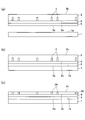
- (A) shows the silicon substrate 2 and the temporary fixed substrate 1 before bonding
- (b) shows an adhesive body in which the silicon substrate 2 and the temporary fixed substrate 1 are bonded
- (c) shows an adhesive silicon This shows a state where the layer 2A is thinned.
- (A) shows a state where the wiring 6 is provided on the silicon layer 2A, and (b) shows a state where the temporary fixed substrate 1 is separated from the silicon substrate.
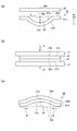
- (A) is a schematic diagram showing a silicon substrate 12 and a curved temporary fixing substrate 11 (before joining), and (b) shows a state where the silicon substrate 12 and the temporary fixing substrate 11 are joined.
- (C) shows the adhesive 14.
- (A) shows a state where the silicon layer 14A of the bonding body is thinned
- (b) shows a bonding body between the silicon layer 14A and the temporary fixing substrate 11A
- (c) shows a state where the silicon layer 12B is formed on the temporary fixing substrate. It shows a state separated from 11A.
- (A) shows the material 20 before processing
- (b) shows the temporary fixed substrate 21 according to the embodiment of the present invention
- (c) is a plan view of the temporary fixed substrate 21.
- (A) is a schematic diagram showing the silicon substrate 22 and the temporary fixed substrate 21 (before joining), (b) shows a state where the silicon substrate 22 and the temporary fixed substrate 21 are joined, and (c) ) Indicates an adhesive body 23.
- FIG. 8 is a schematic diagram showing a temporary fixing substrate 31 having a rectangular shape when viewed in plan.
- (A) shows a state in which the electronic component chip 36 is temporarily fixed by the resin mold 35, and (b) shows a state in which the electronic component 36 and the resin mold 35 are separated from the temporarily fixed substrate 1 by light irradiation.
- a method for temporarily fixing and separating a silicon substrate using a temporarily fixed substrate will be described with reference to FIGS.
- a predetermined conductor 3 is provided on the bonding surface 2a side of the silicon substrate 2.
- the adhesive layer 4 and the release layer 5 are provided on the surface 2a of the silicon substrate 2.
- the bonding surface 1 a of the temporary fixed substrate 1 is opposed to the surface 5 a of the release layer 5.
- the silicon substrate 2 and the temporary fixed substrate 1 are joined to obtain an adhesive.
- the non-bonding surface 2b of the silicon substrate 2 is processed, and the silicon layer 2A is thinned as shown in FIG. 2c is a machined surface.
- the conductor 3A has penetrated the silicon layer 2A.
- a predetermined wiring layer 6 is formed on the silicon substrate 2A.
- Reference numeral 7 denotes a rewiring layer for supplying power to a device chip (electronic component chip) provided on the wiring layer, and is formed by a photo process or a plating method. If necessary, a plurality of device chips are set on this wiring layer (not shown), and then a laser beam having a predetermined wavelength and energy is irradiated from the temporary fixing substrate side. Causes delamination. Thereby, as shown in FIG. 2B, the silicon layer 2A is separated from the temporary fixed substrate together with the adhesive layer 4 and the wiring layer 6, and is subjected to the next processing step.
- the bonded body is curved due to a difference in thermal expansion between the silicon substrate and the temporary fixed substrate.
- the temporary fixing substrate 11 is previously curved in a direction opposite to the direction of the adhesive body. That is, the temporary fixing substrate 11 is curved such that the joint surface 11a of the temporary fixing substrate 11 is recessed and the temporary fixing substrate 11b is expanded.
- 12a is a joint surface
- 12b is a non-joint surface.
- L is an imaginary surface when the temporary fixing substrate 11 is not curved
- W is the amount of curvature.
- the temporary fixing substrate 11 and the silicon substrate 12 are interposed between the jigs 13 and heated while being pressed as indicated by an arrow A.
- a thermosetting adhesive (not shown) is interposed between the temporary fixing substrate 11 and the silicon substrate 12 so that the temporary fixing substrate 11 and the silicon substrate are bonded.
- both the temporarily fixed substrate 11 and the silicon substrate 12 are flattened by heating and pressing.
- an adhesive body 14 of the temporary fixed substrate 11A and the silicon substrate 12A is obtained.
- the temporary fixing substrate 11A is warped to the opposite side from the initial side. This is because the temporary fixed substrate 11A has a larger thermal expansion coefficient than silicon, and therefore contracts during cooling as indicated by an arrow B, and as a result, the entire adhesive body 14 curves toward the opposite side.
- the bending amount W is a plus sign.
- the adhesive 14A is placed on the flat surface 15a of the jig 15, and pressure is applied as shown by an arrow C to process the adhesive while flattening the adhesive.
- the silicon substrate is thinned, a thin silicon layer 12B is formed, and the silicon layer and the temporarily fixed substrate 11A are flattened.
- the adhesive 14A bends again as shown in FIG.
- the amount of curvature W of the adhesive body 14A is smaller than the amount of curvature W before thin plate processing as shown in FIG. 3C, and approaches the curvature of the temporarily fixed substrate before bonding (FIG. a)).
- the silicon layer is separated from the temporarily fixed substrate.
- the shape of the temporary fixed substrate 11A tends to return to the initial shape.
- the silicon layer is thin, it is almost flat.
- the amount of curvature W of the temporary fixed substrate 11 in FIG. 3A can be reduced.
- the amount of curvature W of the bonded body 14 after bonding shown in FIG. (Plus sign opposite to the initial state) can be reduced.
- the amount of bending of the bonded body after bonding may increase (FIG. 3C).
- FIG. 5A shows the material 20 of the temporary fixed substrate.
- the thickness of the temporary fixed substrate material 20 (the distance between the pair of main surfaces 20a and 20b) is constant.
- the material 20 is deformed so that the main surface 20a side is depressed, and the temporary fixed substrate 21 is obtained.
- the thickness of the temporary fixed substrate 21 (the distance between the pair of main surfaces 21a and 21b) is constant.
- An outer peripheral flat plate portion 21 c is provided at a peripheral portion of the temporary fixed substrate 21, and a concave deformation portion 21 d is provided inside the temporary fixed substrate 21.
- the outer peripheral flat plate portion 21c has a ring-shaped flat plate shape, and maintains the shape before processing shown in FIG. L is a virtual surface along the main surface 21a (flat surface 21e) of the outer peripheral flat plate portion 21c.
- the concave deformed portion 21d is deformed downward from the virtual surface L (toward the main surface 21b) and is concave.
- the planar shape of the concave deformed portion 21d is circular.
- the maximum value of the depression of the concave deformed portion 21b from the virtual plane L is defined as the amount of curvature W.
- the bonding surface 22a of the silicon substrate 22 and the bonding surface 21a of the temporary fixed substrate 21 are opposed to each other.
- a predetermined adhesive layer or a release layer can be further formed on the bonding surface 22a side of the silicon substrate 22.
- the temporary fixing substrate 21 and the silicon substrate 22 are sandwiched between the jigs 13, and heated while being pressed as shown by the arrow A.
- a thermosetting adhesive (not shown) is interposed between the temporary fixing substrate 21 and the silicon substrate 22 so that the temporary fixing substrate 21 and the silicon substrate 22 are bonded to each other.
- both the temporarily fixed substrate 21 and the silicon substrate 22 are flattened by heating and pressing.
- the adhesive 23 is placed on the flat surface 15a of the jig 15, and pressure is applied as shown by arrow C to process the adhesive while flattening the adhesive.
- the silicon substrate 22A becomes thinner, a thin silicon layer 22B is formed, and the silicon layer and the temporarily fixed substrate are flattened. 22c is a machined surface.
- the adhesive body 23A bends again as shown in FIG. 7B.
- the temporary fixed substrate is approaching the initial shape. That is, the amount of curvature W of the adhesive body 23A is smaller than the amount of curvature W before thin plate processing as shown in FIG. 6C, and approaches the shape of the temporary fixed substrate before bonding.
- the silicon layer 22B is separated from the temporarily fixed substrate.
- the shape of the temporary fixed substrate 21 tends to return to the initial shape.
- the silicon substrate is thinned, it is almost flat.
- the outer peripheral flat portion 21c is not deformed, and only the concave deformed portion 21d is flatly deformed by the jig 13. Since the outer peripheral flat plate portion has a ring shape and surrounds the concave deformed portion, it acts as an anchor such that the shape of the temporary fixed substrate is not significantly deformed. As a result, the amount of bending after the adhesive 23 is removed from the jig 13 can be reduced (see FIG. 6C).
- the amount of bending after the adhesive 23 is removed from the jig 13 can be reduced.
- the amount of initial bending of the temporary fixed substrate can be reduced. Therefore, handling of each substrate in the bonding equipment is easy, and cracking due to pressure during bonding can be suppressed.
- the silicon substrate is thinned by grinding and polishing (see FIG. 7B), the amount of bending of the adhesive 23A can be reduced, and the subsequent handling of the adhesive is also facilitated. .
- an electronic component is adhered to the fixing surface of the temporary fixing substrate and temporarily fixed by a resin mold.
- an adhesive layer is provided on the fixed surface 1a of the temporary fixed substrate 1.
- examples of such an adhesive include a double-sided tape and a hot-melt adhesive.
- various methods such as roll coating, spray coating, screen printing, and spin coating can be adopted.
- a number of electronic components 36 are placed on the temporary fixing substrate 1 and the adhesive layer is cured to form the adhesive layer 34.
- This curing step is performed according to the properties of the adhesive, and examples thereof include heating and ultraviolet irradiation.
- a liquid resin molding agent is poured in to cure the resin molding agent.
- the electronic component 36 is fixed in the resin mold 35.
- 35b is a resin that fills the gap 37 between the electronic components
- 35a is a resin that covers the electronic components.
- the mold resin include an epoxy resin, a polyimide resin, a polyurethane resin, and a urethane resin.
- the electronic component 36 and the resin mold 35 are separated from the temporary fixed substrate 1 by irradiating light from the bottom surface 1b side of the temporary fixed substrate 1 (see FIG. 9B).
- the wavelength of the light irradiated from the bottom side of the temporary fixed substrate is appropriately changed depending on the type of the electronic component or the resin mold, but may be, for example, 200 nm to 400 nm.
- the material of the temporary fixing substrate is preferably ceramics in terms of mechanical strength and durability against chemicals, and alumina, aluminum nitride, YAG, sialon, and spinel are particularly preferable.
- the material forming the temporary fixed substrate is translucent alumina.
- 100 ppm or more and 300 ppm or less of magnesium oxide powder are added to high-purity alumina powder having a purity of preferably 99.9% or more (preferably 99.95% or more).
- high-purity alumina powder a high-purity alumina powder manufactured by Daimei Chemical Co., Ltd. can be exemplified.
- the purity of the magnesium oxide powder is preferably 99.9% or more, and the average particle size is preferably 50 ⁇ m or less.
- alumina powder it is preferable to add 200 to 800 ppm of zirconia (ZrO 2 ) and 10 to 30 ppm of yttria (Y 2 O 3 ) to the alumina powder as sintering aids.
- ZrO 2 zirconia
- Y 2 O 3 yttria
- the method for forming the temporary fixed substrate is not particularly limited, and may be any method such as a doctor blade method, an extrusion method, and a mold casting method. Particularly preferably, the base substrate is manufactured using a doctor blade method.
- a slurry containing a ceramic powder, a dispersion medium, and a binder is produced, and the slurry is formed into a tape shape by a doctor blade method, which is laminated and punched into a desired thickness shape.
- a molded body is obtained.
- the molded body is dried, preferably calcined in the atmosphere, and then calcined in hydrogen.
- the sintering temperature during the main firing is preferably from 1700 to 1900 ° C., more preferably from 1750 to 1850 ° C., from the viewpoint of densification of the sintered body.
- the surface of the sintered body is polished with a diamond wrap or the like to adjust the thickness unevenness to be equal to or less than a predetermined value, and both surfaces are mirror-finished.
- the annealing temperature is preferably 1700 ° C. or less from the viewpoint of preventing deformation and abnormal grain growth, and more preferably the maximum temperature is 1600 ° C. or less.
- the temperature is preferably 1200 ° C. or more, more preferably 1400 ° C. or more.
- the annealing time is preferably 1 to 6 hours.
- the glass constituting the temporary fixing substrate may be a silicate glass or a borosilicate glass.
- the temporary fixed substrate of the present invention has an outer peripheral flat plate portion and a concave deformed portion surrounded by the outer peripheral flat plate portion, and the fixing surface is a flat surface in the outer peripheral flat plate portion.
- the width F of the outer peripheral flat plate portion (see FIGS. 5B and 5C) is preferably not less than 4% of the width R of the temporary fixed substrate 21, thereby suppressing the amount of bending of the adhesive. The effect is higher. From this viewpoint, the width F of the outer peripheral flat plate portion is more preferably 8% or more of the width R of the temporary fixed substrate 21, and particularly preferably 10% or more.
- the width F of the outer peripheral flat plate portion is preferably 60% or less of the width R of the temporary fixed substrate 21, thereby increasing the effect of suppressing the amount of bending of the adhesive. From this viewpoint, the width F of the outer peripheral flat plate portion is more preferably 40% or less of the width R of the temporary fixed substrate 21, and particularly preferably 30% or less.
- the width R of the temporary fixed substrate is the length of a line segment that crosses the temporary fixed substrate in a plane.
- the width F of the outer peripheral flat plate portion is the total value of the lengths of the line segments that cross the outer peripheral flat plate portion among the line segments that cross the temporary fixed substrate in a plane.
- the width of each of the two outer peripheral flat portions in the width direction of the temporary fixed substrate is F / 2, but in this case, the width of the outer peripheral flat portion is F / 2.
- (F / 2 + F / 2) F.
- the width R of the temporary fixed substrate and the width F of the outer peripheral flat plate portion may change depending on the direction of the line segment traversing the temporary fixed substrate.
- the planar shape of the temporary fixed substrate 31 is rectangular, and the thickness of the temporary fixed substrate 31 (the distance between the main surface 31a and the opposite main surface) is constant.
- An outer peripheral flat portion 31c is provided at the peripheral edge of the temporary fixed substrate 31, and a concave deformed portion 31d is provided inside the outer peripheral flat portion 31c.
- the outer peripheral flat portion 31c has a flat plate shape, and the main surface 31a of the outer peripheral flat portion 31 constitutes a flat surface 31e.
- the concave deformed portion 31d is deformed downward from the virtual surface and is concave.
- the planar shape of the concave deformed portion 31d is a rectangle.
- the width R2 in the vertical direction and the width R1 in the horizontal direction are different, and the width F2 of the outer peripheral flat plate portion in the vertical direction (F2 / 2 + F2 / 2).
- the width F1 (F1 / 2 + F1 / 2) of the outer peripheral flat portion in the lateral direction may be different.
- the width of the outer peripheral flat plate portion / the width of the temporary fixed substrate (F1 / R1, F2 / R2) is 4 to 60% in both the vertical and horizontal directions.
- the amount of curvature W of the concave deformed portion is 0.1 mm or more, whereby the amount of curvature of the adhesive can be suppressed. From this viewpoint, the amount of curvature W of the concave deformation portion is more preferably 0.3 mm or more, and particularly preferably 0.6 mm or more.
- the contour in the cross section can be an arc, a parabola, a cone, or a dish.
- the contour of the cross section of the concave deformed portion is parabolic. Further, by making the boundary between the outer flat portion and the curved portion gentle (increase the radius of curvature R), it is possible to suppress the occurrence of cracks when bonding to the silicon substrate.
- the amount of curvature of the concave deformed portion is 2.5 mm or less, thereby suppressing a problem of handling into the bonding apparatus and preventing breakage during bonding. easy. From this viewpoint, the amount of curvature of the concave deformation portion is preferably equal to or less than 2.0 mm, and more preferably equal to or less than 1.0 mm.
- the thickness unevenness (so-called TTV) of the entire temporary fixed substrate is large, the thickness unevenness of the adhesive layer occurs at the time of bonding with the silicon substrate or the electronic component chip, which causes deformation after bonding.
- the thickness unevenness is preferably 10 ⁇ m or less.
- the thickness unevenness is preferably 5 ⁇ m or less, more preferably 3 ⁇ m or less.
- the amount of curvature of the concave deformed portion is measured as follows. That is, the virtual surface L is obtained by extending the fixed surface (flat surface) of the outer peripheral flat portion onto the concave deformed portion. Then, the depth of the deepest portion of the concavely deformed portions viewed from the virtual plane L is defined as the amount of curvature W.
- the amount of curvature W is defined as the amount of curvature W.
- each of the temporary fixed substrate, the silicon substrate, and the like may have the same plane shape and plane dimension as each other, or may have different plane shapes and plane dimensions.
- each of the temporary fixed substrate, the silicon substrate, and the like may be a disk, a rectangle, an ellipse, an ellipse, a triangle, a polygon, or the like.
- it is preferable that each of the temporary fixed substrate and the silicon substrate is a disk shape or a regular polygon shape, and it is more preferable that the temporary fixed substrate and the silicon substrate are point symmetric, and it is more preferable that the silicon substrate is a disk shape. In this case, thermal contraction occurs uniformly in each direction around the point symmetry axis.
- the diameter (width) is preferably set to 100 to 300 mm.
- the orientation flat and the notch are formed on the silicon substrate, if the same orientation flat and the notch are also formed on the temporary fixing substrate, the positioning at the time of bonding can be easily performed, and the defective bonding can be reduced.
- the temporary fixed substrate and the silicon substrate are square or rectangular, the length of one side thereof is preferably 100 to 1000 mm. In this case, it is preferable that the corners have an R or C shape from the viewpoint of suppressing the amount of bending after bonding.
- the thickness of the temporary fixed substrate is, for example, preferably from 0.2 to 5.0 mm, and more preferably from 0.5 to 2.0 mm.
- the thickness is easy to suppress warpage after bonding, and it is easy to prevent the temporary fixing substrate from being damaged. Further, by setting this to 5.0 mm or less, the weight of the substrate is suppressed, and the transfer becomes easy.
- the temporary fixing substrate and the silicon substrate etc. are overlapped and heated in a state where they are pressed and fixed to cure the thermosetting adhesive. Thereby, an adhesive body is obtained.
- Examples of the adhesive for bonding the temporary fixing substrate and the silicon substrate include a thermosetting resin, a UV (ultraviolet curing) adhesive, a double-sided tape, a hot melt adhesive, and the like. Further, as a method of providing the adhesive on the temporary fixing substrate, various methods such as roll coating, spray coating, screen printing, and spin coating can be adopted.
- a release layer between the adhesive layer and the temporary fixing substrate.
- a release layer in addition to a laser release type in which the release layer is carbonized by laser light irradiation and peeled off, a UV release type in which the UV light is deactivated and loses tackiness and peels off due to irradiation, In this case, a heat-peelable type in which the components in the layer foam and peel off can be adopted.
- Various electronic component structures can be manufactured on the silicon substrate of the present invention.
- a wiring layer is formed by bonding a silicon substrate to a temporary fixed substrate, thinning the silicon substrate, and then performing a thin film forming step and a patterning step.
- the present invention is particularly useful because if the curvature of the adhesive body between the temporary fixing substrate and the silicon substrate is large, it is difficult to pattern a fine wiring structure with high precision in the patterning step.
- electronic component chips can be placed on a silicon substrate, and each electronic component chip can be electrically connected to a wiring layer. After the silicon substrate is separated from the temporary fixed substrate, the electronic component chips can be separated by cutting the silicon substrate.
- the present invention can be suitably applied to so-called FOWLP technology.
- FOWLP technology electronic component chips are temporarily relocated on a support wafer (temporary fixed substrate), sealed with a resin mold, wiring is formed on the surface of the resin mold, and then the electronic component chip and mold resin are supported. By peeling off from the wafer (temporary fixed substrate), a thin structure can be realized. Then, after separating the resin mold and the electronic component chip sealed therein from the temporary fixing substrate, the resin mold is cut, and each electronic component chip can be separated. Also in this case, when the resin sealing of the electronic component chip and the wiring formation on the temporary fixed substrate are performed, the problem of the curvature of the adhesive caused by the difference in thermal expansion between the respective members becomes problematic. Can improve this.
- the curvature of the adhesive caused by a difference in thermal expansion between the temporary fixing substrate and the electronic component chip becomes a problem. Can be improved.
- the area occupied by the electronic component chip with respect to the area of the temporary fixed substrate exceeds 60%, this tendency becomes remarkable, and the present invention is useful.
- a grinder When thinning the silicon substrate by processing, a grinder can be used. In other words, a desired thickness can be obtained by fixing the temporary fixed substrate side of the bonded body of the temporary fixed substrate and the silicon substrate with a vacuum chuck or the like and processing the silicon substrate side with a grinding wheel.
- Examples 1 to 7 A slurry was prepared by mixing the following components.
- (Raw material powder) ⁇ 100 parts by mass of ⁇ -alumina powder having a purity of 99.99% ⁇ MgO (magnesia) 250 ppm ⁇ ZrO2 (zirconia) 400ppm ⁇ Y2O3 (yttria) 15ppm
- (Dispersion medium) ⁇ 45 parts by mass of 2-ethylhexanol (binder) ⁇ PVB resin 4 parts by mass (dispersant) ⁇ 3 parts by mass of polymer surfactant (plasticizer) ⁇ DOP 0.1 parts by mass
- the material 20 was sandwiched between jigs having a predetermined shape, and heat-treated at a temperature of 1600 ° C. and deformed to obtain a temporary fixed substrate 21 (see FIGS. 5B and 5C).
- the diameter (width) of the temporary fixed substrate, the width of the outer peripheral flat plate portion, and the amount of curvature W were variously changed as shown in Table 1 by changing the molding conditions and the shape of the jig.
- Example 3 The same experiment as in Example 1 was performed. However, in this example, the shape of the jig at the time of the heat treatment was adjusted, and the outer peripheral flat plate portion was not provided on the temporary fixed substrate. Further, the diameter ⁇ and the amount of curvature W of the temporary fixed substrate were variously changed as shown in Table 2 by changing the molding conditions and the shape of the jig. The width of the outer peripheral flat portion is 0 mm.
- the amount of bending of the adhesive is small even if the amount of bending of the temporary fixing substrate is the same as that of the comparative example. Further, by setting the ratio of the width of the outer peripheral flat portion to 4 to 60%, the effect of the present invention became more remarkable.
- the respective temporary fixed substrates of Examples 1 to 7 were manufactured, electronic component chips were bonded, and sealed with a resin mold. Otherwise, in the same manner as in Examples 1 to 7, the electronic component chip and the resin mold were separated from the temporarily fixed substrate. Then, the resin mold was cut to obtain each electronic component chip. The presence or absence of cracks at the time of bonding (visual observation) and the amount of bending of the bonded body after bonding were measured, and the same results as in Examples 1 to 7 were obtained.
Landscapes
- Mechanical Treatment Of Semiconductor (AREA)
- Adhesives Or Adhesive Processes (AREA)
- Container, Conveyance, Adherence, Positioning, Of Wafer (AREA)
Abstract
【課題】シリコン基板等を接着し、仮固定するための固定面と、固定面の反対側にある底面とを備え、セラミックスからなる仮固定基板において、仮固定基板をシリコン基板に接着した後の接着体の湾曲量を低減する。 【解決手段】仮固定基板21は、シリコン基板と電子部品チップとの少なくとも一方を接着し、仮固定するための固定面21aと、固定面の反対側にある底面21bとを備え、セラミックスまたはガラスからなる。仮固定基板21は、外周平板部21cと、外周平板部によって包囲された凹状変形部21dとを有する。固定面21aが、外周平板部において平坦面21eである。
Description
本発明は、シリコン基板の仮固定基板、仮固定方法および電子部品の製造方法に関するものである。
近年、電子部品の小型化、低背化への要求が強まっており、その製造のためのシリコン基板についても、極端に薄くした状態で用いられるケースが多くなっている。この際、薄くしたシリコン基板は、剛性が不足し、搬送、研削・研磨といったプロセスに耐えられないため、ガラスやセラミックスからなる仮固定基板を用いてシリコン基板を支持する方法が知られている(特許文献1、2、3)。
これらの従来技術では、熱硬化性樹脂によってシリコン基板を仮固定基板に対して接着し、冷却した後、シリコン基板を研削・研磨により薄板化する。次いで、さらに表面への多層配線形成等を行い、その後、仮固定基板からシリコン基板を剥がし、所望の寸法にダイシングする。接着層にあらかじめ剥離層を設けておき、仮固定基板側から剥離層に対してレーザー光をあてることで、シリコン基板を仮固定基板から剥離させる。
シリコン基板を仮固定基板上に熱硬化性樹脂で接着する際、シリコン基板と仮固定基板との熱膨張差によって、接着体に反りが発生する。このため、特許文献2では、支持基板を予め接着体の反りとは逆方向に湾曲させておくことで、接着体の反りを少なくすることが試みられている。支持基板の反りは、加熱変形、研磨方法の変更、加工変質層の除去によって調節している。
しかし、熱硬化性樹脂の種類、接着温度、仮固定基板とシリコン基板の厚み、といった条件の制約から、接着後の接着体の湾曲量が大きくなることがある。この場合には、仮固定基板の反対側への初期の湾曲量を、接着体の湾曲量に応じて大きくしておく必要がある。しかし、そうした場合、接合の際に、接合設備での各基板のハンドリングが難しくなったり、接合時の圧力で割れることがあった。また、接着体を得た後、シリコン基板を研削・研磨により薄くすると、接着体の湾曲量はシリコン基板に接着する前の仮固定基板の初期の湾曲量に近づく。このため、接着直後の接着体の湾曲量にくらべて湾曲量が大きくなり、その後のプロセスを実施することが困難となる。
本発明の課題は、シリコン基板や電子部品チップを接着し、仮固定するための固定面と、固定面の反対側にある底面とを備える仮固定基板において、仮固定基板をシリコン基板や電子部品チップに接着した後の接着体の湾曲量を一層低減できるようにすることである。
本発明は、シリコン基板と電子部品チップとの少なくとも一方を接着し、仮固定するための固定面と、前記固定面の反対側にある底面とを備え、セラミックスまたはガラスからなる仮固定基板であって、
外周平板部と、前記外周平板部によって包囲された凹状変形部とを有しており、前記固定面が前記外周平板部において平坦面であることを特徴とする。
外周平板部と、前記外周平板部によって包囲された凹状変形部とを有しており、前記固定面が前記外周平板部において平坦面であることを特徴とする。
また、本発明は、前記仮固定基板の前記固定面に前記シリコン基板と電子部品チップとの少なくとも一方を接着して接着体を得る工程、および
前記シリコン層を前記仮固定基板から分離する工程
を有することを特徴とする。
前記シリコン層を前記仮固定基板から分離する工程
を有することを特徴とする。
また、本発明は、前記仮固定基板の前記固定面に前記シリコン基板を接着して接着体を得る工程、
前記シリコン層内または前記シリコン層上に電子部品チップを設ける工程、および
前記シリコン層および電子部品チップを前記仮固定基板から分離する工程
を有することを特徴とする、電子部品の製造方法に係るものである。
前記シリコン層内または前記シリコン層上に電子部品チップを設ける工程、および
前記シリコン層および電子部品チップを前記仮固定基板から分離する工程
を有することを特徴とする、電子部品の製造方法に係るものである。
また、本発明は、前記仮固定基板の前記固定面に前記電子部品チップを接着して接着体を得る工程、および
前記電子部品チップを前記仮固定基板から分離する工程
を有することを特徴とする、電子部品の製造方法に係るものである。
前記電子部品チップを前記仮固定基板から分離する工程
を有することを特徴とする、電子部品の製造方法に係るものである。
本発明によれば、シリコン基板と電子部品チップとの少なくとも一方を接着し、仮固定するための固定面と、固定面の反対側にある底面とを備え、セラミックスからなる仮固定基板において、仮固定基板の初期の湾曲が同じであっても、仮固定基板をシリコン基板や電子部品チップに接着した後の接着体の湾曲量を一層低減できる。この結果、仮固定基板の初期の湾曲量を過度に大きくしておく必要がなく、接合設備での各基板のハンドリングが容易であり、接合時の圧力で割れることも抑制できる。また、接着体を得た後、例えばシリコン基板を研削・研磨により薄くした後、接着体の湾曲量を小さくでき、この後の接着体のハンドリングも容易となる。
最初に、図1、図2を参照しつつ、仮固定基板を用いたシリコン基板の仮固定および分離方法について述べる。
まず、図1(a)に示す例では、シリコン基板2の接合面2a側に所定の導体3を設けておく。そして、シリコン基板2の表面2a上に接着層4、剥離層5を設ける。仮固定基板1の接合面1aを剥離層5の表面5aに対向させる。
まず、図1(a)に示す例では、シリコン基板2の接合面2a側に所定の導体3を設けておく。そして、シリコン基板2の表面2a上に接着層4、剥離層5を設ける。仮固定基板1の接合面1aを剥離層5の表面5aに対向させる。
次いで、図1(b)に示すように、シリコン基板2と仮固定基板1とを接合し、接着体を得る。次いで、シリコン基板2の非接合面2bを加工し、図1(c)に示すようにシリコン層2Aを薄くする。2cは加工面である。本例では、シリコン層2Aを薄くした時点で、導体3Aはシリコン層2Aを貫通している。
次いで、図2(a)に示すように、シリコン基板2A上に所定の配線層6を形成する。7は、配線層の上に設置するデバイスチップ(電子部品チップ)に給電するための再配線層であり、フォトプロセスやめっき法により形成される。この配線層の上に必要に応じ、複数のデバイスチップを設置(図示せず)し、次いで、仮固定基板側から所定波長およびエネルギーのレーザ光を照射し、剥離層5で仮固定基板1の剥離を生じさせる。これによって、図2(b)に示すように、シリコン層2Aは、接着層4、配線層6とともに仮固定基板から分離され、次の処理工程に供される。
ここで、シリコン基板を仮固定基板上に熱硬化性樹脂で接着する際、シリコン基板と仮固定基板との熱膨張差によって、接着体に湾曲が発生する。このため、図3(a)に示すように、仮固定基板11を、予め接着体の湾曲とは逆方向に湾曲させておく方法が知られている。すなわち、仮固定基板11の接合面11aが凹み、11bが膨らむように、仮固定基板11を湾曲させる。12aは接合面であり、12bは非接合面である。ここで、Lは、仮固定基板11が湾曲していない場合の仮想面であり、Wは湾曲量であるが、接合面が凹んでいる場合にはマイナス符号とし,接合面が突出している場合にはプラス符号とする。
次いで、図3(b)に示すように、治具13の間に仮固定基板11、シリコン基板12をはさみ、矢印Aのように加圧しながら加熱する。好ましくは仮固定基板11とシリコン基板12との間に、図示しない熱硬化性接着剤を介在させ、効果させることで、仮固定基板11とシリコン基板とを接着する。この時点では、加熱および加圧によって仮固定基板11、シリコン基板12はともに平坦な状態になる。
接合が終了すると、図3(c)に示すように、仮固定基板11Aとシリコン基板12Aとの接着体14が得られる。ただし、接着体においては、仮固定基板11Aは、初期とは反対側に反っている。これは、仮固定基板11Aのほうが熱膨張係数がシリコンよりも大きいので、冷却時に矢印Bのように収縮し、この結果、接着体14の全体が反対側に向かって湾曲するからである。湾曲量Wはプラス符号となる。
次いで、図4(a)に示すように、治具15の平坦面15a上に接着体14Aを乗せ、矢印Cのように圧力を加えて接着体を平坦にしつつ加工する。これによって、シリコン基板が薄くなって、薄いシリコン層12Bが形成されるとともに、シリコン層および仮固定基板11Aは平坦化する。次いで,接着体14Aを治具15から取り外すと、図4(b)に示すように接着体14Aは再び湾曲する。ただし、接着体14Aの湾曲量Wは、図3(c)に示すような薄板加工前の湾曲量Wよりも小さくなっており、接合前の仮固定基板の湾曲に近づいている(図3(a))。
次いで、図4(c)に示すように、仮固定基板からシリコン層を分離する。このとき、仮固定基板11Aの形状は初期形状に戻る傾向がある。一方、シリコン層は薄板化しているので、ほぼ平坦となっている。
ここで、図3(a)における仮固定基板11の初期の湾曲量Wをマイナス符号方向に大きく設定しておくことによって、図3(c)に示す接合後の接着体14の湾曲量W(初期と反対のプラス符号)を小さくすることができる。しかし、熱硬化性樹脂の種類、接着温度、仮固定基板とシリコン基板の厚み、といった条件の制約から、接着後の接着体の湾曲量が大きくなることがある(図3(c))。この場合には、仮固定基板の反対側への初期の湾曲量を、接着体の湾曲量に応じて大きくしておく必要がある(図3(a))。しかし、そうした場合、図3(b)に示す接合の際に、接合設備での各基板のハンドリングが難しくなったり、接合時の圧力で割れることがあった。また、接着体を得た後、シリコン基板を研削・研磨により薄くすると、接着体の湾曲量はシリコン基板に接着する前の仮固定基板の初期の湾曲量に近づく(図4(b))。このため、接着直後の接着体の湾曲量にくらべて湾曲量が大きくなり、その後のプロセスを実施することが困難となる。
図5~図8は、本発明の実施例に係るものである。
図5(a)は、仮固定基板の材料20を示す。仮固定基板材料20の厚さ(一対の主面20aと20bとの間隔)は一定である。
図5(a)は、仮固定基板の材料20を示す。仮固定基板材料20の厚さ(一対の主面20aと20bとの間隔)は一定である。
次いで、図5(b)、(c)に示すように、材料20の主面20a側が凹むように変形させ、仮固定基板21を得る。ここで、仮固定基板21の厚さ(一対の主面21aと21bとの間隔)は一定である。仮固定基板21の周縁部には外周平板部21cが設けられており、仮固定基板21の内側に凹状変形部21dが設けられている。外周平板部21cはリング状の平板形状をなしており、図5(a)に示す加工前の形態を維持している。Lは外周平板部21cの主面21a(平坦面21e)に沿った仮想面である。一方、凹状変形部21dは、仮想面Lから下側(主面21b側)へと向かって変形し、凹んでいる。本例では、凹状変形部21dの平面形状は円形である。凹状変形部21bの仮想面Lからの凹みの最大値を湾曲量Wとする。
図6(a)に示す例では、シリコン基板22の接合面22aと仮固定基板21の接合面21aとを対向させる。なお、シリコン基板22の接合面22a側には所定の接着剤層や剥離層を更に形成できる。次いで、図6(b)に示すように、治具13の間に仮固定基板21、シリコン基板22をはさみ、矢印Aのように加圧しながら加熱する。仮固定基板21とシリコン基板22との間には、図示しない熱硬化性接着剤を介在させ、効果させることで、仮固定基板21とシリコン基板22とを接着する。この時点では、加熱および加圧によって仮固定基板21、シリコン基板22はともに平坦な状態になる。
接合が終了すると、図6(c)に示すように、仮固定基板21Aとシリコン基板22Aとの接着体23が得られる。ただし、接着体においては、仮固定基板21Aは、初期とは反対側に沿っている。これは、仮固定基板21Aのほうが熱膨張係数がシリコンよりも大きいので、冷却時に矢印Bのように収縮し、この結果、接着体23の全体が反対側に向かって湾曲するからである。
次いで、図7(a)に示すように、治具15の平坦面15a上に接着体23を乗せ、矢印Cのように圧力を加えて接着体を平坦にしつつ加工する。これによって、シリコン基板22Aが薄くなって、薄いシリコン層22Bが形成されるとともに、シリコン層および仮固定基板は平坦化する。22cは加工面である。次いで,接着体23Aを治具15から取り外すと、図7(b)に示すように接着体23Aは再び湾曲する。ただし、仮固定基板は、初期の形状に近づいている。すなわち、接着体23Aの湾曲量Wは、図6(c)に示すような薄板加工前の湾曲量Wよりも小さくなっており、接合前の仮固定基板の形状に近づいている。
次いで、図7(c)に示すように、仮固定基板からシリコン層22Bを分離する。このとき、仮固定基板21の形状は初期形状に戻る傾向がある。一方、シリコン基板は薄板化しているので、ほぼ平坦となっている。
ここで、本発明においては、図6(a)に示すように、仮固定基板の初期の湾曲量が同じであっても、仮固定基板をシリコン基板に接着したときに(図6(b)参照)、外周平板部21cは変形せず、凹状変形部21dのみが治具13によって平坦に変形する。そして、外周平板部はリング状をなしており、凹状変形部を包囲していることから、仮固定基板の形状が大きく変形しないようなアンカーとして作用する。この結果、接着体23を治具13から取り外した後の湾曲量を低減できる(図6(c)参照)。
この結果、仮固定基板の初期の湾曲量が同等であっても、接着体23を治具13から取り外した後の湾曲量を低減できる。また、接着体23を治具13から取り外した後の湾曲量が同等である場合には、仮固定基板の初期の湾曲量を低減できる。ゆえに、接合設備での各基板のハンドリングが容易であり、接合時の圧力で割れることも抑制できる。また、接着体を得た後、シリコン基板を研削・研磨により薄くした後(図7(b)参照))、接着体23Aの湾曲量を小さくでき、この後の接着体のハンドリングも容易となる。
以下、本発明の仮固定基板を電子部品チップの接着に利用した実施形態について述べる。
まず、仮固定基板の前記固定面に電子部品を接着し、樹脂モールドによって仮固定する。例えば、図9(a)に示すように、仮固定基板1の固定面1a上に接着剤層を設ける。こうした接着剤としては、両面テープやホットメルト系の接着剤などを例示できる。また、接着剤層を仮固定基板上に設ける方法としては、ロール塗布、スプレー塗布、スクリーン印刷、スピンコートなど種々の方法を採用できる。
まず、仮固定基板の前記固定面に電子部品を接着し、樹脂モールドによって仮固定する。例えば、図9(a)に示すように、仮固定基板1の固定面1a上に接着剤層を設ける。こうした接着剤としては、両面テープやホットメルト系の接着剤などを例示できる。また、接着剤層を仮固定基板上に設ける方法としては、ロール塗布、スプレー塗布、スクリーン印刷、スピンコートなど種々の方法を採用できる。
次いで、仮固定基板1上に多数の電子部品36を設置し、接着剤層を硬化させて接着層34を形成する。この硬化工程は、接着剤の性質に合わせて行うが、加熱、紫外線照射を例示できる。
次いで、液状の樹脂モールド剤を流し込み、樹脂モールド剤を硬化させる。これによって、図9(a)に示すように、樹脂モールド35内に電子部品36を固定する。ただし、35bは、電子部品の隙間37を充填する樹脂であり、35aは、電子部品を被覆する樹脂である。
モールド樹脂としては、エポキシ系樹脂、ポリイミド系樹脂、ポリウレタン系樹脂、ウレタン系樹脂などが挙げられる。
モールド樹脂としては、エポキシ系樹脂、ポリイミド系樹脂、ポリウレタン系樹脂、ウレタン系樹脂などが挙げられる。
次いで、矢印Aに示すように、仮固定基板1の底面1b側から光を照射することによって、仮固定基板1から電子部品36および樹脂モールド35を分離する(図9(b)参照)。
仮固定基板の底面側から照射する光の波長は電子部品や樹脂モールドの種類によって適宜変更するが、例えば200nm~400nmとすることができる。
仮固定基板の底面側から照射する光の波長は電子部品や樹脂モールドの種類によって適宜変更するが、例えば200nm~400nmとすることができる。
以下、本発明の各構成要素について更に述べる。
仮固定基板の材質は、機械的強度および薬品に対する耐久性の点からセラミックスが好ましく、アルミナ、窒化アルミニウム、YAG、サイアロン、スピネルが特に好ましい。
仮固定基板の材質は、機械的強度および薬品に対する耐久性の点からセラミックスが好ましく、アルミナ、窒化アルミニウム、YAG、サイアロン、スピネルが特に好ましい。
好適な実施形態においては、仮固定基板を構成する材料が透光性アルミナである。この場合、好ましくは純度99.9%以上(好ましくは99.95%以上)の高純度アルミナ粉末に対して、100ppm以上、300ppm以下の酸化マグネシウム粉末を添加する。このような高純度アルミナ粉末としては、大明化学工業株式会社製の高純度アルミナ粉体を例示できる。また、この酸化マグネシウム粉末の純度は99.9%以上が好ましく、平均粒径は50μm以下が好ましい。
また、好適な実施形態においては、焼結助剤として、アルミナ粉末に対して、ジルコニア(ZrO2)を200~800ppm、イットリア(Y2O3)を10~30ppm添加することが好ましい。
仮固定基板の成形方法は特に限定されず、ドクターブレード法、押し出し法、モールドキャスト法など任意の方法であってよい。特に好ましくは、ベース基板をドクタープレード法を用いて製造する。
好適な実施形態においては、セラミック粉末、分散媒および結合剤を含むスラリーを製造し、このスラリーをドクターブレード法によりテープ状に成型し、これを所望の厚さ形状になるように積層、打ち抜きすることで成形体を得る。
次いで、成形体を乾燥し、好ましくは大気中で仮焼し、次いで、水素中で本焼成する。本焼成時の焼結温度は、焼結体の緻密化という観点から、1700~1900℃が好ましく、1750~1850℃が更に好ましい。この焼結体をダイヤラップ等により表面研磨を行い、厚さムラを一定以下となるように調整するとともに、両面を鏡面化する。
このように焼成時に十分に緻密な焼結体を生成させた後に、厚さムラの調整、表面を鏡面化した上でアニール処理を実施することで精度よく湾曲量の調整を行うことができる。このアニール温度は、変形や異常粒成長発生を防止するといった観点から1700℃以下であることが好ましく、最高温度が1600℃以下であることが更に好ましい。一方で焼結体のクリープ変形を十分に行い、湾曲量を精度よく調整するためには1200℃以上が好ましく、1400℃以上であることが更に好ましい。また、アニール時間は、1~6時間であることが好ましい。
また、仮固定基板を構成するガラスは、珪酸塩系ガラスや硼珪酸塩系ガラスであってよい。
本発明の仮固定基板は、外周平板部と、外周平板部によって包囲された凹状変形部とを有しており、前記固定面が前記外周平板部において平坦面である。ここで、外周平板部の幅F(図5(b)、(c)参照)は、仮固定基板21の幅Rの4%以上であることが好ましく、これによって接着体の湾曲量を抑制する効果が高くなる。この観点からは、外周平板部の幅Fは、仮固定基板21の幅Rの8%以上であることが更に好ましく、10%以上であることが特に好ましい。
また、外周平板部の幅Fは、仮固定基板21の幅Rの60%以下であることが好ましく、これによって接着体の湾曲量を抑制する効果が高くなる。この観点からは、外周平板部の幅Fは、仮固定基板21の幅Rの40%以下であることが更に好ましく、30%以下であることが特に好ましい。
なお、仮固定基板の幅Rは、仮固定基板を平面的に横断する線分の長さである。また、外周平板部の幅Fは、仮固定基板を平面的に横断する前記線分のうち、前記外周平板部を横断する線分の長さの合計値である。例えば、図5(c)に示すような平面図においては、仮固定基板の幅方向の2箇所の外周平板部の幅はそれぞれF/2であるが、この場合には外周平板部の幅は、(F/2+F/2)=Fとなる。
また、仮固定基板を横断する線分の方向によっては仮固定基板の幅R、外周平板部の幅Fが変化する場合がある。例えば図8に示す例では、仮固定基板31の平面形状が長方形であり、仮固定基板31の厚さ(主面31aと反対側の主面との間隔)は一定である。仮固定基板31の周縁部には外周平板部31cが設けられており、外周平板部31cの内側に凹状変形部31dが設けられている。外周平板部31cは平板形状をなしており、外周平板部31の主面31aは平坦面31eを構成している。凹状変形部31dは、仮想面から下側へと向かって変形し、凹んでいる。本例では、凹状変形部31dの平面形状は長方形である。例えば、仮固定基板の平面形状が長方形である場合には、縦方向の幅R2と横方向の幅R1とは異なっている上、縦方向の外周平板部の幅F2(F2/2+F2/2)と横方向の外周平板部の幅F1(F1/2+F1/2)とが異なる場合がある。この場合には、縦方向と横方向とで(外周平板部の幅/仮固定基板の幅(F1/R1、F2/R2)がそれぞれ4~60%であることが好ましい。
接合前の仮固定基板においては、凹状変形部の湾曲量Wが0.1mm以上であることが好ましく、これによって接着体の湾曲量を抑制できる。この観点からは、凹状変形部の湾曲量Wは0.3mm以上であることが更に好ましく、0.6mm以上であることが特に好ましい。
また、凹状変形部の形状については、断面における輪郭を、円弧状、放物線状、円錐状、皿状とすることができる。ただし、湾曲量の抑制を効果的に行うためには、凹状変形部の断面における輪郭が放物線状であることが好ましい。また、外周平坦部と湾曲部の境界部分を緩やかにする(曲率半径Rを大きくする)ことで、シリコン基板と接着する際、クラックの発生を抑制することができる。
また、接合前の仮固定基板においては、凹状変形部の湾曲量が2.5mm以下であることが好ましく、これによって接合装置内へのハンドリングの問題が抑えられ、また接合時の破損を防止し易い。この観点からは、凹状変形部の湾曲量は2.0mm以下であることが好ましく、1.0mm以下であることが更に好ましい。
このとき、仮固定基板全体における厚みムラ(いわゆるTTV)が大きいと、シリコン基板や電子部品チップとの貼り合わせの際、接着層の厚みムラが発生し、接着後の変形の原因となるため、厚みムラは10um以下が好ましい。また、接着されたシリコン基板や電子部品チップに高精度の配線形成を行う場合、厚みムラは5um以下が好ましく、3um以下であることが更に好ましい。
なお、凹状変形部の湾曲量は以下のようにして測定する。すなわち、外周平板部の固定面(平坦面)を凹状変形部上に延長することで仮想面Lを得る。そして、仮想面Lから見て凹状変形部のうちら最も深い部分の深さを湾曲量Wと定義する。また、具体的な測定装置としては、平坦なテーブル上に設置した基板の形状をレーザー測長機で計測することで可能となる。
仮固定基板とシリコン基板等のそれぞれの平面形状、平面寸法は特に限定されない。仮固定基板とシリコン基板等とは、互いに同じ平面形状、平面寸法を有していてもよいし、異なる平面形状、平面寸法を有していてもよい。具体的には、例えば、仮固定基板、シリコン基板等のそれぞれは、円板状であってもよいし、矩形状、長円状、楕円状、三角形状、多角形状などであってもよい。なかでも、仮固定基板とシリコン基板のそれぞれが、円板状、正多角形状である場合のように、点対称であることが好ましく、円板状であることがさらに好ましい。この場合は、点対称軸を中心として各方位で均等に熱収縮が生じる。
なお、仮固定基板、シリコン基板等が円板状である場合は、その直径(幅)は、100~300mmとすることが好ましい。シリコン基板にオリフラやノッチが形成されている場合、仮固定基板にも同様のオリフラやノッチを形成すると、接着の際の位置決めがしやすく、接着ズレ不良を低減することができる。また、仮固定基板、シリコン基板が正方形または長方形である場合は、その一辺の長さは、100~1000mmとすることが好ましい。この場合、角部はRまたはC形状とすることが、接着後の湾曲量を抑制するとの観点から好ましい。
仮固定基板の厚さは、例えば、0.2~5.0mmであることが好ましく、0,5~2.0mmであることが更に好ましい。これを0.2mm以上とすることによって、接着後の反り抑制がし易くなるとともに、仮固定基板の破損を防止し易くなる。また、これを5.0mm以下とすることによって、基板重量が抑えられ、搬送がしやすくなる。
仮固定基板とシリコン基板等とを熱硬化性樹脂を用いて接合する場合は、仮固定基板とシリコン基板等とを重ね合わせて加圧固定した状態で加熱して熱硬化性接着剤を硬化させることにより、接着体を得る。
仮固定基板とシリコン基板等とを接着する接着剤としては、熱硬化性樹脂の他、UV(紫外線硬化型)接着剤、両面テープやホットメルト系の接着剤などを例示できる。また、接着剤を仮固定基板上に設ける方法としては、ロール塗布、スプレー塗布、スクリーン印刷、スピンコートなど種々の方法を採用できる。
また、接着層と仮固定基板との間に剥離層を形成することが好ましい。こうした剥離層としては、レーザー光の照射により剥離層が炭化して剥離するレーザー剥離型のものに加え、UV光の照射により失活し、粘着性が失われ剥離するUV剥離型のもの、加熱により層内の成分が発泡し剥離する加熱剥離型のものも採用できる。
本発明のシリコン基板には、各種電子部品構造を作製できる。例えばCCDやCMOSを作製する場合は、仮固定基板にシリコン基板を接合した後に、シリコン基板を薄くし、次いで薄膜形成工程及びパターニング工程を行うことによって配線層を形成する。この際、仮固定基板とシリコン基板との接着体の湾曲が大きいと、パターニング工程において、微細な配線構造を高精度にパターニングすることが難しいため、本発明は特に有用である。
また、シリコン基板上に電子部品チップを設置し、各電子部品チップと配線層とを電気的に接続することができる。そして、シリコン基板を仮固定基板から分離した後に、シリコン基板を割断することによって、各電子部品チップを分離することができる。
また、本発明は、いわゆるFOWLP技術に対して好適に適用できる。FOWLP技術においては、電子部品チップを一旦サポートウェハー(仮固定基板)上に再配置し、樹脂モールドで封止した後、樹脂モールドの表面に配線を形成し、次いで電子部品チップおよびモールド樹脂をサポートウェハー(仮固定基板)から剥離することで、薄型構造の実現が可能となる。そして、樹脂モールドおよびこれに封止された電子部品チップを仮固定基板から分離した後に、樹脂モールドを割断し、各電子部品チップをそれぞれ分離することができる。この場合においても、仮固定基板上で電子部品チップの樹脂封止、配線形成を行った際に各部材のとの熱膨張差によって生じる接着体の湾曲が問題となるが、本発明を用いることでこれを改善することができる。
また、仮固定基板に接着する電子部品を大面積化した場合には、仮固定基板と電子部品チップとの熱膨張差によって生じる接着体の湾曲が問題となるが、本発明を用いることでこれを改善することができる。特に仮固定基板の面積に対する電子部品チップが占める面積が60%を超えるとこの傾向が顕著となるため、本発明が有用である。
仮固定基板に外周平板部と凹状変形部とを形成する際には、外周平板部に適合する平坦部と凹状変形部に適合する突起とを有する治具を準備し、仮固定基板を加熱しながら治具を押しつけることによって塑性変形させる。あるいは、同様の平坦部と突起とを有する金型中に平板を収容し、加熱しながら金型を押圧することで、外周平板部と凹状変形部とを形成できる。
シリコン基板を加工によって薄くする際には、グラインダーを用いることができる。すなわち、仮固定基板とシリコン基板の接着体の、仮固定基板側をバキュームチャック等で固定し、シリコン基板側を研削砥石で加工することで、所望の厚さとすることができる。
(実施例1~7)
以下の成分を混合したスラリーを調製した。
(原料粉末)
・純度99.99%のα-アルミナ粉末 100質量部
・MgO(マグネシア) 250ppm
・ZrO2(ジルコニア) 400ppm
・Y2O3(イットリア) 15ppm
(分散媒)
・2-エチルヘキサノール 45質量部
(結合剤)
・PVB樹脂 4質量部
(分散剤)
・高分子界面活性剤 3質量部
(可塑剤)
・DOP 0.1質量部
以下の成分を混合したスラリーを調製した。
(原料粉末)
・純度99.99%のα-アルミナ粉末 100質量部
・MgO(マグネシア) 250ppm
・ZrO2(ジルコニア) 400ppm
・Y2O3(イットリア) 15ppm
(分散媒)
・2-エチルヘキサノール 45質量部
(結合剤)
・PVB樹脂 4質量部
(分散剤)
・高分子界面活性剤 3質量部
(可塑剤)
・DOP 0.1質量部
このスラリーを、ドクターブレード法を用いて焼成後の厚さに換算して0.7mmとなるようテープ状に成形し、焼成後の大きさに換算してφ300mmとなるよう切断した。得られた粉末成形体を、大気中1240℃で仮焼(予備焼成)の後、基板をモリブデン製の板に載せ、水素3:窒素1の雰囲気中で、1800℃で2.5時間保持し、焼成を行った。その後、グラインダーによる研削、ダイヤモンド砥粒によるラップ、CMPリキッドによる研磨を順に行い、厚さ0.6mmの仮固定基板材料20を得た(図5(a))。
次いで、材料20を所定の形状の冶具に挟み、1600℃の温度で熱処理し、変形させることで、仮固定基板21を得た(図5(b)(c)参照)。
得られた仮固定基板と同じ径のシリコン基板とを熱硬化性樹脂で接着し、その際のクラック発生有無、接着後の湾曲量を測定した。ただし、剥離層は加熱剥離型接着剤を用いた。次いで、シリコン基板を0.1mm厚まで研削加工し、研削後の接着体の湾曲量を測定した。
ただし、成形条件や治具の形状を変更することによって、仮固定基板の直径(幅)、外周平板部の幅、湾曲量Wを、表1に示すように種々変更した。
そして、各例について、接着時のクラックの有無(目視)、接着後の接着体の湾曲量、シリコン基板を研削加工した後の接着体の湾曲量をそれぞれ測定した。測定結果を表1に示す。

(比較例1~3)
実施例1と同様の実験を行った。ただし、本例では、熱処理の際の冶具形状を調整し、仮固定基板に外周平板部を設けなかった。また、成形条件や治具の形状を変更することによって、仮固定基板の直径φ、湾曲量Wを、表2に示すように種々変更した。外周平板部の幅は0mmとなる。
実施例1と同様の実験を行った。ただし、本例では、熱処理の際の冶具形状を調整し、仮固定基板に外周平板部を設けなかった。また、成形条件や治具の形状を変更することによって、仮固定基板の直径φ、湾曲量Wを、表2に示すように種々変更した。外周平板部の幅は0mmとなる。
そして、各例について、接着時のクラックの有無(目視)、接着後の接着体の湾曲量、シリコン基板を研削加工した後の接着体の湾曲量をそれぞれ測定した。測定結果を表2に示す。

外周平板部のない比較例の仮固定基板を使用した場合には、接着体の湾曲量が相対的に大きくなっており、シリコン基板の研磨後の湾曲量も大きくなっている。
本発明の仮固定基板を使用した場合には、仮固定基板の湾曲量が比較例と同じであっても、接着体の湾曲量が小さくなっている。また、外周平板部の幅の比率を4~60%とすることで、本発明の効果が一層顕著になっていた。
また、実施例1~7の各仮固定基板を製造し、電子部品チップを接着し、樹脂モールドで封止した。他は実施例1~7と同様にして電子部品チップおよび樹脂モールドを仮固定基板から分離した。そして樹脂モールドを割断して各電子部品チップを得た。接着時のクラックの有無(目視)、接着後の接着体の湾曲量をそれぞれ測定したが、実施例1~7と同様の結果を得た。
Claims (13)
- シリコン基板と電子部品チップとの少なくとも一方を接着し、仮固定するための固定面と、前記固定面の反対側にある底面とを備え、セラミックスまたはガラスからなる仮固定基板であって、
外周平板部と、前記外周平板部によって包囲された凹状変形部とを有しており、前記固定面が前記外周平板部において平坦面であることを特徴とする、仮固定基板。 - 前記セラミックスが透光性アルミナであることを特徴とする、請求項1記載の仮固定基板。
- 前記外周平板部の幅が前記仮固定基板の幅の4~60%であることを特徴とする、請求項1または2記載の仮固定基板。
- 前記凹状変形部の湾曲量が0.1~2.5mmであることを特徴とする、請求項1~3のいずれか一つの請求項に記載の仮固定基板。
- 請求項1~4のいずれか一つの請求項に記載の仮固定基板の前記固定面に前記シリコン基板と前記電子部品チップとの少なくとも一方を接着して接着体を得る工程
を有することを特徴とする、仮固定方法。 - 前記接着体の前記シリコン基板を加工してシリコン基板を薄くし、シリコン層を形成する工程、および
前記シリコン層を前記仮固定基板から分離する工程
を有することを特徴とする、請求項5記載の方法。 - 前記シリコン層に電子部品構造を設ける工程を有することを特徴とする、請求項5または6記載の方法。
- 前記仮固定基板の前記固定面に前記電子部品チップを接着した後、前記電子部品チップを樹脂モールドで覆う工程を有していることを特徴とする、請求項5記載の方法。
- 請求項1~4のいずれか一つの請求項に記載の仮固定基板の前記固定面に前記シリコン基板を接着して接着体を得る工程、
前記シリコン層内または前記シリコン層上に電子部品チップを設ける工程、および
前記シリコン層および前記電子部品チップを前記仮固定基板から分離する工程
を有することを特徴とする、電子部品の製造方法。 - 前記シリコン層を前記仮固定基板から分離した後、前記シリコン層を分割する工程を有することを特徴とする、請求項9記載の方法。
- 前記シリコン層内に配線を設け、この配線を前記電子部品チップと接続する工程を有することを特徴とする、請求項9または10記載の方法。
- 請求項1~4のいずれか一つの請求項に記載の仮固定基板の前記固定面に前記電子部品チップを接着して接着体を得る工程、および
前記電子部品チップを前記仮固定基板から分離する工程
を有することを特徴とする、電子部品の製造方法。 - 前記仮固定基板の前記固定面に前記電子部品チップを接着した後、前記電子部品チップを樹脂モールドで覆う工程を有していることを特徴とする、請求項12記載の方法。
Priority Applications (1)
| Application Number | Priority Date | Filing Date | Title |
|---|---|---|---|
| JP2020532437A JP7266036B2 (ja) | 2018-07-26 | 2019-07-24 | 仮固定基板、仮固定方法および電子部品の製造方法 |
Applications Claiming Priority (2)
| Application Number | Priority Date | Filing Date | Title |
|---|---|---|---|
| JP2018-139956 | 2018-07-26 | ||
| JP2018139956 | 2018-07-26 |
Publications (1)
| Publication Number | Publication Date |
|---|---|
| WO2020022372A1 true WO2020022372A1 (ja) | 2020-01-30 |
Family
ID=69181691
Family Applications (1)
| Application Number | Title | Priority Date | Filing Date |
|---|---|---|---|
| PCT/JP2019/028976 Ceased WO2020022372A1 (ja) | 2018-07-26 | 2019-07-24 | 仮固定基板、仮固定方法および電子部品の製造方法 |
Country Status (3)
| Country | Link |
|---|---|
| JP (1) | JP7266036B2 (ja) |
| TW (1) | TWI814872B (ja) |
| WO (1) | WO2020022372A1 (ja) |
Citations (5)
| Publication number | Priority date | Publication date | Assignee | Title |
|---|---|---|---|---|
| JPS63261831A (ja) * | 1987-04-03 | 1988-10-28 | ビービーシー ブラウン ボヴェリ アクチェンゲゼルシャフト | 層の接合方法及び接合を実施するための装置 |
| JPH08316300A (ja) * | 1995-05-23 | 1996-11-29 | Sumitomo Metal Mining Co Ltd | 電子デバイス用支持板 |
| JP2011023438A (ja) * | 2009-07-14 | 2011-02-03 | Nippon Electric Glass Co Ltd | 基板接合体の製造方法 |
| JP2015220302A (ja) * | 2014-05-16 | 2015-12-07 | 株式会社ディスコ | サポートプレート、サポートプレートの形成方法及びウェーハの加工方法 |
| JP2016076650A (ja) * | 2014-10-08 | 2016-05-12 | トヨタ自動車株式会社 | 半導体装置の製造方法 |
Family Cites Families (6)
| Publication number | Priority date | Publication date | Assignee | Title |
|---|---|---|---|---|
| US7094666B2 (en) * | 2004-07-29 | 2006-08-22 | Silicon Genesis Corporation | Method and system for fabricating strained layers for the manufacture of integrated circuits |
| US7427554B2 (en) * | 2005-08-12 | 2008-09-23 | Silicon Genesis Corporation | Manufacturing strained silicon substrates using a backing material |
| TWI340446B (en) * | 2005-12-30 | 2011-04-11 | Advanced Semiconductor Eng | Method and device for preventing warpage of a substrate strip during semiconductor packaging and the substrate strip |
| FR2965974B1 (fr) * | 2010-10-12 | 2013-11-29 | Soitec Silicon On Insulator | Procédé de collage moléculaire de substrats en silicium et en verre |
| WO2013023708A1 (de) * | 2011-08-12 | 2013-02-21 | Ev Group E. Thallner Gmbh | Vorrichtung und verfahren zum bonden von substraten |
| WO2017155002A1 (ja) * | 2016-03-11 | 2017-09-14 | ボンドテック株式会社 | 基板接合方法 |
-
2019
- 2019-07-24 WO PCT/JP2019/028976 patent/WO2020022372A1/ja not_active Ceased
- 2019-07-24 JP JP2020532437A patent/JP7266036B2/ja active Active
- 2019-07-25 TW TW108126305A patent/TWI814872B/zh active
Patent Citations (5)
| Publication number | Priority date | Publication date | Assignee | Title |
|---|---|---|---|---|
| JPS63261831A (ja) * | 1987-04-03 | 1988-10-28 | ビービーシー ブラウン ボヴェリ アクチェンゲゼルシャフト | 層の接合方法及び接合を実施するための装置 |
| JPH08316300A (ja) * | 1995-05-23 | 1996-11-29 | Sumitomo Metal Mining Co Ltd | 電子デバイス用支持板 |
| JP2011023438A (ja) * | 2009-07-14 | 2011-02-03 | Nippon Electric Glass Co Ltd | 基板接合体の製造方法 |
| JP2015220302A (ja) * | 2014-05-16 | 2015-12-07 | 株式会社ディスコ | サポートプレート、サポートプレートの形成方法及びウェーハの加工方法 |
| JP2016076650A (ja) * | 2014-10-08 | 2016-05-12 | トヨタ自動車株式会社 | 半導体装置の製造方法 |
Also Published As
| Publication number | Publication date |
|---|---|
| JP7266036B2 (ja) | 2023-04-27 |
| TWI814872B (zh) | 2023-09-11 |
| JPWO2020022372A1 (ja) | 2021-08-02 |
| TW202030851A (zh) | 2020-08-16 |
Similar Documents
| Publication | Publication Date | Title |
|---|---|---|
| KR101142000B1 (ko) | 정전척 | |
| EP2960925B1 (en) | Semiconductor device and method for manufacturing semiconductor device | |
| TWI514441B (zh) | A substrate substrate, a composite substrate for a semiconductor, a semiconductor circuit substrate, and a method of manufacturing the same | |
| JP3904943B2 (ja) | サファイアウエハーの加工方法及び電子装置の製造方法 | |
| KR20250145080A (ko) | 가고정 기판 및 가고정 기판의 제조 방법 | |
| KR101642671B1 (ko) | 반도체용 복합 기판의 핸들 기판 및 반도체용 복합 기판 | |
| TWI815002B (zh) | 暫時固定基板、複合基板及電子構件的剝離方法 | |
| JP7266036B2 (ja) | 仮固定基板、仮固定方法および電子部品の製造方法 | |
| CN110494956A (zh) | 临时固定基板以及电子部件的模塑方法 | |
| JP7698792B2 (ja) | 仮固定基板、仮固定基板の製造方法、および仮固定方法 | |
| JP7303081B2 (ja) | 仮固定基板、複合基板および電子部品の剥離方法 | |
| CN110462804B (zh) | 临时固定基板以及电子部件的临时固定方法 | |
| JP2023149989A (ja) | 仮固定基板、仮固定基板の製造方法、および電子部品の仮固定方法 | |
| WO2026074917A1 (ja) | 仮固定基板および仮固定基板の製造方法 | |
| WO2026074915A1 (ja) | 仮固定基板および仮固定基板の製造方法 | |
| JP5094467B2 (ja) | セラミック基板の製造方法 | |
| CN118398564A (zh) | 芯片结构及其制备方法 |
Legal Events
| Date | Code | Title | Description |
|---|---|---|---|
| 121 | Ep: the epo has been informed by wipo that ep was designated in this application |
Ref document number: 19840986 Country of ref document: EP Kind code of ref document: A1 |
|
| ENP | Entry into the national phase |
Ref document number: 2020532437 Country of ref document: JP Kind code of ref document: A |
|
| NENP | Non-entry into the national phase |
Ref country code: DE |
|
| 122 | Ep: pct application non-entry in european phase |
Ref document number: 19840986 Country of ref document: EP Kind code of ref document: A1 |