WO2020008976A1 - ペリクル複合体及びその製造方法 - Google Patents
ペリクル複合体及びその製造方法 Download PDFInfo
- Publication number
- WO2020008976A1 WO2020008976A1 PCT/JP2019/025422 JP2019025422W WO2020008976A1 WO 2020008976 A1 WO2020008976 A1 WO 2020008976A1 JP 2019025422 W JP2019025422 W JP 2019025422W WO 2020008976 A1 WO2020008976 A1 WO 2020008976A1
- Authority
- WO
- WIPO (PCT)
- Prior art keywords
- film
- pellicle
- carbon
- substrate
- frame
- Prior art date
- Legal status (The legal status is an assumption and is not a legal conclusion. Google has not performed a legal analysis and makes no representation as to the accuracy of the status listed.)
- Ceased
Links
Images

Classifications
-
- G—PHYSICS
- G03—PHOTOGRAPHY; CINEMATOGRAPHY; ANALOGOUS TECHNIQUES USING WAVES OTHER THAN OPTICAL WAVES; ELECTROGRAPHY; HOLOGRAPHY
- G03F—PHOTOMECHANICAL PRODUCTION OF TEXTURED OR PATTERNED SURFACES, e.g. FOR PRINTING, FOR PROCESSING OF SEMICONDUCTOR DEVICES; MATERIALS THEREFOR; ORIGINALS THEREFOR; APPARATUS SPECIALLY ADAPTED THEREFOR
- G03F1/00—Originals for photomechanical production of textured or patterned surfaces, e.g., masks, photo-masks, reticles; Mask blanks or pellicles therefor; Containers specially adapted therefor; Preparation thereof
- G03F1/62—Pellicles, e.g. pellicle assemblies, e.g. having membrane on support frame; Preparation thereof
-
- G—PHYSICS
- G03—PHOTOGRAPHY; CINEMATOGRAPHY; ANALOGOUS TECHNIQUES USING WAVES OTHER THAN OPTICAL WAVES; ELECTROGRAPHY; HOLOGRAPHY
- G03F—PHOTOMECHANICAL PRODUCTION OF TEXTURED OR PATTERNED SURFACES, e.g. FOR PRINTING, FOR PROCESSING OF SEMICONDUCTOR DEVICES; MATERIALS THEREFOR; ORIGINALS THEREFOR; APPARATUS SPECIALLY ADAPTED THEREFOR
- G03F1/00—Originals for photomechanical production of textured or patterned surfaces, e.g., masks, photo-masks, reticles; Mask blanks or pellicles therefor; Containers specially adapted therefor; Preparation thereof
- G03F1/62—Pellicles, e.g. pellicle assemblies, e.g. having membrane on support frame; Preparation thereof
- G03F1/64—Pellicles, e.g. pellicle assemblies, e.g. having membrane on support frame; Preparation thereof characterised by the frames, e.g. structure or material, including bonding means therefor
Definitions
- the present invention relates to a pellicle complex and a method for producing the same.
- the miniaturization of semiconductor devices is progressing year by year, and patterns with a line width of about 45 nm have been achieved by excimer exposure.
- a pattern having a smaller width for example, a line width of about 32 nm or less has been demanded, and accordingly, it has been studied to change the exposure light to extreme ultraviolet (EUV, Extreme Ultra Violet) having a shorter wavelength.
- EUV extreme ultraviolet
- a resist is exposed by EUV reflected by a photomask (reticle, working mask, or the like) reflecting an exposure pattern.
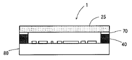
- a pellicle complex provided with a dust-proof protective film is used for the photomask (for example, Patent Documents 1 and 2). As shown in FIG.
- the pellicle composite 1 of Patent Documents 1 and 2 is provided on a pattern forming surface of a photomask 80, and includes a pellicle film 25 functioning as a dust-proof film, and a pellicle film 25. And a frame 40 provided on the outer edge.
- the pellicle film 25 of Patent Document 1 is a DLC
- the pellicle film 25 of Patent Document 2 is a graphene film or a graphite thin film, and the pellicle film 25 and the frame 40 are bonded with an adhesive 70.
- the pellicle composite as described above has problems in durability, outgas generation, resistance to hydrogen radicals, and the like.
- the present invention has been made in view of the above circumstances, and an object thereof is to improve at least one (preferably all) of durability, outgas generation, and hydrogen radical resistance.
- the present inventors have conducted intensive studies to solve the above-mentioned problems, and as a result, it has been found that the decrease in durability and the generation of outgas are attributable to the adhesive, and that a part of the pellicle film is a carbon film, When a film composed of a predetermined element is formed on the frame side of the film and the two are surface-bonded, the peel strength between the two can be maintained at a predetermined value or more without using an adhesive, and the hydrogen radical resistance of the pellicle film is also improved.
- the present invention was found to be able to increase the durability, to improve the durability, to reduce the outgassing, and the like, and to complete the present invention. That is, the present invention is as follows.
- the element constituting the frame (C) is at least one element selected from the group consisting of silicon, zirconium, niobium, molybdenum, titanium, and tungsten.
- [5] The pellicle composite according to any one of [1] to [4], wherein the carbon film (A) is a carbonaceous film or a graphite film (A1).
- a laminate obtained by laminating a carbonized material film (A ′) on one surface of a substrate (C ′) made of the same material as the frame portion (C) is heated to convert the carbonized material film (A ′) to a carbon film ( After A), the laminated body is etched from the substrate (C ′) side to leave the outer edge of the substrate (C ′) thicker than other portions, thereby forming the frame portion (C),
- a laminate obtained by laminating a carbonized raw material film (A ′) on one surface of a substrate (C ′) made of the same material as the frame portion (C) is heated to convert the carbonized raw material film (A ′) to carbonaceous material.
- the carbon film (A) and the film portion (B) are changed to two layers of a film or a graphite film (A1) and a layer (B2) containing both elements and carbon constituting the frame portion (C).
- the pellicle composite of the present invention at least one (preferably all) of durability, outgassing, and hydrogen radical resistance can be improved.
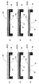
- FIG. 1 is a schematic sectional view showing an example of the pellicle complex of the present invention.
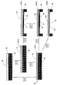
- FIG. 2 is a schematic flow chart showing an example of the method for producing a pellicle composite of the present invention.
- FIG. 3 is a schematic flow chart showing another example of the method for producing a pellicle composite of the present invention.
- FIG. 4 is a schematic cross-sectional view showing a photomask provided with a conventional pellicle composite.
- EUV Extreme UV
- EUV Extreme Ultra Violet
- EUV as used herein means light having a wavelength of 5 nm to 30 nm, preferably 5 nm to 13.5 nm.
- the pellicle composite of the present invention is preferably used for the EUV lithography method.
- the pellicle complex is used to protect a pattern surface of a photomask reflecting an exposure pattern, and includes a pellicle film and a frame portion (pellicle frame) provided on an outer edge of the pellicle film. Be composed.
- the shape of the pellicle film is not particularly limited, and can be appropriately selected from a circle, an ellipse, a polygon, and the like. A preferred shape is a square such as a square or a rectangle.
- Pellicle film The film portion of the pellicle complex. In the present invention, it is composed of a carbon film (A) and a film part (B). The film part (B) will be described later.
- the carbon film (A) means a film substantially composed of carbon atoms, and is used as a constituent member of the pellicle film in the present invention.
- the thickness of the carbon film is, for example, 1,000 nm or less, preferably 5 nm to 100 nm, more preferably 5 nm to 50 nm, and particularly preferably 5 nm to 30 nm.
- the area of the carbon film is, for example, 100 cm 2 or more, preferably 120 cm 2 or more, and more preferably 150 cm 2 or more and 3000 cm 2 or less.
- the shape of the carbon film is not particularly limited, it is preferably a rectangle or a square, and the length of one side is, for example, 10 cm or more, preferably 15 cm or more, and more preferably 20 cm or more.
- the carbon film transmittance of EUV having a wavelength of 13.5 nm is, for example, 55% or more and 97% or less, preferably 74% or more and 97% or less, and more preferably 84% or more and 97% or less.
- the surface roughness (Sa) of the carbon film is, for example, 0.1 nm or more and 500 nm or less.
- the surface roughness is preferably 0.2 nm or more, more preferably 0.5 nm or more, further preferably 1 nm or more, and preferably 200 nm or less, more preferably 100 nm or less, and even more preferably 50 nm or less.
- the surface roughness Sa means an arithmetic average height obtained based on ISO 25178.
- the EUV transmittance improves as the surface roughness decreases.
- the carbon film includes a carbonaceous film, a diamond-like carbon film (DLC), a graphene film, a graphite film, and the like, and the carbonaceous film includes an amorphous carbon film, an amorphous carbon film, and the like.
- Preferred carbon films are a carbonaceous film, a graphene film, a graphite film and the like, and more preferred are a carbonaceous film and a graphite film (A1).
- the carbonaceous film can be distinguished from the graphene film or the graphite film based on the results of the laser Raman measurement.
- a G band due to the graphite structure appears around 1575 to 1600 cm -1
- a D band due to the amorphous carbon structure appears around 1350 to 1360 cm -1 .
- the ratio (I (D) / I (G); D / G band intensity ratio) between the G band intensity (I (G)) and the intensity of the D band (I (D)) in the Raman spectrum is 0.5.
- Those exceeding the above are classified as carbonaceous films, and those having a D / G band intensity ratio of 0.5 or less are classified as graphene films or graphite films.
- the D / G band intensity ratio of the carbonaceous film is preferably 2.5 or less, more preferably 0.7 or more and 1.5 or less, and particularly preferably 0.9 or more and 1.3 or less.
- the D / G band intensity ratio of Glassy @ carbon which is a typical amorphous carbon produced by a method such as vapor deposition or sputtering, is about 1.8 to 2.0.
- a carbonaceous film having a D / G band intensity ratio of 1.5 or less can be obtained or manufactured by an appropriate method, and for example, is preferably manufactured by carbonizing an aromatic polyimide film.
- the aromatic polyimide film is made of, for example, a polyamic acid prepared by combining pyromellitic dianhydride, 4,4-diaminodiphenyl ether (ODA), and p-phenylenediamine (PDA) with an acid anhydride such as acetic anhydride.
- ODA 4,4-diaminodiphenyl ether
- PDA p-phenylenediamine
- a film obtained by a chemical cure method in which imidization is performed using a dehydrating agent typified by a substance or a tertiary amine such as picoline, quinoline, isoquinoline, or pyridine as an imidization accelerator is preferable.
- the carbonization treatment (heat treatment) of the aromatic polyimide film may be performed at about 900 to 2000 ° C.
- the heating rate up to the carbonization temperature is not particularly limited, but is, for example, 5 ° C./min or more and 15 ° C./min or less.
- the material may be cooled to room temperature by natural cooling or the like.
- the thickness of the carbonaceous film can be selected from the same range as the thickness of the carbon film described above.
- the surface roughness (Sa) of the carbonaceous film is the same as the surface roughness (Sa) of the carbon film.
- the D / G band intensity ratio of the graphene film or the graphite film is 0 or more and 0.5 or less, preferably 0 or more and 0.1 or less, more preferably 0 or more and 0.05 or less.
- Examples of the graphene film include a graphene single-layer film and a graphene multilayer film having a thickness of less than 5 nm.
- the graphite film is a film having a thickness of 5 nm or more, and the preferable range of the thickness is the same as the preferable range of the carbon film.
- the surface roughness (Sa) of the graphite film is the same as the surface roughness (Sa) of the carbon film described above.
- the graphene film or the graphite film is formed by heating a carbonaceous film obtained from the aromatic polyimide film at a temperature higher than the carbonization temperature, for example, higher than 2000 ° C. and 3300 ° C. or lower, preferably 2200 ° C. or higher and 3200 ° C. or lower, more preferably 2400 ° C. or higher and 3000 or higher. It can be obtained by performing heat treatment at a temperature of not more than °C.
- the pellicle frame means a frame formed on the pellicle film, and is used to cover the photomask with the pellicle complex.
- the pellicle frame may have a vent to keep the pressure inside the exposure apparatus and inside the pellicle complex constant.
- the material of the pellicle frame include elements such as cesium, potassium, sodium, and rubidium which form an intercalation compound with a carbon film, and elements which dissolve (solid-dissolve) carbon such as nickel, bismuth, and iron or dissolve in carbon. Although it may be present, it preferably contains an element consisting of silicon, zirconium, niobium, molybdenum, titanium, and tungsten.
- Silicon, molybdenum, titanium, tungsten, and the like are elements that form a metal carbide (metal carbide), and are more preferable than elements that hardly react with carbon atoms such as zirconium and niobium. It is preferable that these elements are the most numerous elements among the elements constituting the frame (excluding carbon, hydrogen, oxygen, and nitrogen).
- semimetals or metals such as silicon, zirconium, niobium, molybdenum, titanium, and tungsten are preferable, and metals such as zirconium, niobium, molybdenum, titanium, and tungsten are more preferable.
- FIG. 1A is a schematic cross-sectional view showing an example of the pellicle complex 1 of the present invention.
- the pellicle complex 1 (2) as an example is a carbonaceous film (A1) as a carbon film (A) 20. 21 and a frame (C) 40 provided along the outer edge of the carbon film 20 (21).
- the pellicle complex 2 includes a film portion (B) 30 surface-bonded to one side (the side where the frame portion (C) 40 exists) of the carbon film (A) 20, and the film in the illustrated example is provided.
- the portion (B) 30 is a film portion (hereinafter, referred to as “homogeneous film” (B1)) 31 which is made of the same material as the frame portion (C) 40 and is integrated with the frame portion (C) 40.
- the film part (B) 30 (31) and the carbon film (A) 20 (21) are surface-bonded, the two are directly bonded, so that the peel strength between them can be more than a predetermined value without using an adhesive. Can be maintained. In addition, it is possible to prevent a decrease in durability and outgas generation due to the adhesive. Further, since the carbon film 20 (21) is protected by the film portion 30 (31), the hydrogen radical resistance can be increased.
- the thickness of the carbon film (A) 20 (in the illustrated example, the thickness of the carbonaceous film (A1) 21) is as described above in the column of terms.
- the thickness of the film portion (B) 30 (in the illustrated example, the thickness of the homogeneous film (B1) 31) is, for example, 0.5 nm to 100 nm, preferably 0.5 nm to 10 nm, and more preferably 0.5 nm. Not less than 5 nm.
- the surface roughness of the carbon film (A) 20 (in the illustrated example, the surface roughness of the carbonaceous film (A1) 21) is as described above in the term column.
- the surface roughness means the roughness on the outer surface side (the side opposite to the contact surface with the film portion 30) of the carbon film (A) 20.
- the surface roughness (Sa) of the outer surface of the film portion (B) 30 (in the illustrated example, the homogeneous film (B1) 31) (that is, the surface roughness on the side not in contact with the carbon film (A) 20) is, for example, 0.
- the bonding strength between the carbon film (A) 20 and the film part (B) 30 is sufficient if the strength does not cause the two to peel off during production or use of the pellicle composite 1. It is preferable that the strength is such that material destruction (for example, material destruction of the carbon film (A) 20) occurs earlier than interface destruction when a peeling test is performed.
- the film part (B) 30 does not need to be made of the same material as that of the frame part (C) 40, and it is sufficient that the film part (B) 30 contains at least a part of the constituent elements of the frame part (C) 40.
- the film part (B) 30 has a two-layer structure, and the two-layer structure is a homogeneous film ( B1) 31 and a film (hereinafter referred to as “frame element / carbon-containing film” (B2)) 35 on the carbonaceous film (A1) 21 side.
- the film (B2) 35 contains both the elements constituting the frame (C) 40 and carbon.
- the film (B2) 35 contains carbon, the bonding property with the carbon film (A) 20 (in the illustrated example, the carbonaceous film (A1) 21) is further improved, and the film (B2) 35 is formed of the frame portion (C).
- the bonding property with the frame portion (C) 40 is further improved.
- Examples of the frame element / carbon-containing film (B2) 35 include various films depending on the elements constituting the frame.
- the element constituting the frame portion (hereinafter, sometimes referred to as “frame element”) is a metal element or a metalloid element
- a metal carbide film or a metalloid metal carbide film can be given, and these are a metal carbide and a metalloid.
- It may be a layer containing carbide or the like. Further, it may be a layer containing an interlayer compound between the frame element and the carbon film, or a layer in which carbon is dissolved in the frame element.
- it is a metal carbide film.
- the formation of the metal carbide film is performed using mapping of element distribution which can be measured by scanning transmission electron microscopy (STEM) and energy dispersive X-ray spectroscopy (EDS: energy dispersive X-ray spectrometry).
- STEM scanning transmission electron microscopy
- EDS energy dispersive X-ray spectrometry
- a pellicle complex cut out to several mm square using a laser marker is used. After the cut-out pellicle complex is embedded in a resin such as epoxy, the pellicle complex is cut together with the resin so that the cross section of the pellicle complex is exposed, and processed into a sample for cross-sectional TEM measurement.
- the shaving of the cross section is not a mechanical process such as polishing or cutting that affects the shape of the cross section, but is, for example, a focused ion beam (FIB), an electron beam (EB), or an Ar ion beam (EB). It is desirable to use a method that can perform cross-section processing with high precision, such as Ar Ion Beam). STEM / EDS analysis is performed on the sample whose cross section has been processed to confirm the formation of a metal carbide film and measure the film thickness. At the same time, confirmation of the carbon film and the homogeneous film and measurement of the film thickness can be performed.
- FIB focused ion beam
- EB electron beam
- EB Ar ion beam
- the total thickness of the two layers is the same as the thickness of the film part (B) 30 described above.
- the thickness of the film (homogeneous film (B1) 31 in the illustrated example) on the frame (C) 40 side of the film portion (B) 30 having a two-layer structure is, for example, 0.3 nm or more and 60 nm or less, preferably It is 0.3 nm or more and 6 nm or less, more preferably 0.3 nm or more and 3 nm or less.
- the thickness of the film (the frame element / carbon-containing film (B2) 35 in the illustrated example) on the carbon film (A) 20 side is, for example, 0.2 nm or more and 40 nm.
- the thickness is preferably from 0.2 nm to 4 nm, more preferably from 0.2 nm to 2 nm.
- the film part (B) 30 of the pellicle complex 4 illustrated in FIG. 1C is composed of a frame element / carbon-containing film (B2) 35. As shown in the illustrated example, the homogeneous film (B1) 31 is not essential.
- the pellicle complex 5 in FIG. 1D is obtained by changing the carbonaceous film (A1) 21 of the pellicle complex 2 in FIG. 1A to a graphite film (A1) 22.
- the pellicle complex 6 of FIG. 1E is obtained by changing the carbonaceous film (A1) 21 of the pellicle complex 3 of FIG. 1B to a graphite film (A1) 22.
- the pellicle complex 7 in FIG. 1F is obtained by changing the carbonaceous film (A1) 21 of the pellicle complex 4 in FIG. 1C to a graphite film (A1) 22.
- the carbon film (A) 20 may be a carbonaceous film (A1) 21 or a graphite film (A1) 22.
- various films can be used as the carbon film (A) 20 as long as the film is substantially composed of carbon atoms.
- FIG. 2 is a schematic flow chart for explaining a method for manufacturing the pellicle complexes 2 to 4 of FIGS. 1A to 1C.
- a carbonized raw material film (A ′) 50 is laminated on one surface of a substrate (C ′) 45 having the same material as the frame portion 40 to produce a first laminate 60.
- the carbonized raw material film (A ') 50 a known carbonized raw material can be used, and preferably, the above-mentioned aromatic polyimide film can be used.
- the obtained first laminate 60 is heated at a carbonization temperature (for example, about 900 to 2000 ° C. when the carbonized raw material film (A ′) 50 is an aromatic polyimide film) (carbonization step: S11).
- a carbonization temperature for example, about 900 to 2000 ° C. when the carbonized raw material film (A ′) 50 is an aromatic polyimide film
- carbonization step: S11 carbonization step: S11
- the second laminate 61 in which the carbonized raw material film (A ′) 50 has been changed to the carbonaceous film (A1) 21 is obtained.
- etching step: S13 By etching while masking the outer edge of the substrate (C ′) of the second stacked body 61 (etching step: S13), the frame part (C) 40 and the film part (B) 30 are formed, and the pellicle composite is formed. 2 can be manufactured.
- a part of the substrate (C ′) remains as a homogeneous film (B 1) 31 while being etched away. Details
- the product (third laminate 62) of the carbonization step S12 is obtained by treating the second laminate 61 under a carbonization condition stronger (higher temperature, longer time, etc.) than the production condition. However, it can be produced (carbonization step: S16).
- step S13 By performing the same etching as in step S13 (etching step: S14) while masking the outer edge of the substrate (C ′) of the obtained third stacked body 62 (etching step: S14), the frame part (C) 40 and the film part ( B) 30 is formed, and the pellicle complex 3 can be manufactured.
- step S15 By increasing the etching conditions, the homogeneous film (B1) 31 of the film part (B) 30 can be removed (etching step: S15), and the pellicle composite 4 can be manufactured.
- the first laminate 61 can be formed directly (that is, without going through the carbonization step) by a vapor deposition method or a sputtering method.
- the pellicle complex 3 can also be manufactured by subjecting the pellicle complex 2 to a carbonizing treatment having the same strength as in steps S12 and S16 (carbonizing step: S17).
- FIG. 3 is a schematic flow chart for explaining a method for producing the pellicle complexes 5 to 7 shown in FIGS. 1 (d) to 1 (f).
- the third laminate 62 obtained in the production example of FIG. 2 is treated at a graphitization temperature (for example, higher than 2000 ° C. and 3300 ° C. or lower) (graphitization step: S21).
- a fourth laminate 63 in which the carbonaceous film (A1) 21 is replaced with the graphite film (A1) 22 is manufactured.
- the fourth laminate 63 is obtained by treating the first laminate 60 at a graphitization temperature (graphitization step: S22), or treating the second laminate 61 at a graphitization temperature (graphitization). Step: S23) It is also possible to manufacture.
- the obtained fourth stacked body 63 is processed in the same etching step as the step S14 (etching step: S24), or is processed in the same etching step as the step S15 (etching step: S25).
- the pellicle complex 6 or the pellicle complex 7 can be manufactured.
- the substrate (C ′) 45 can be formed without the frame element / carbon-containing film (B2) 35 interposed therebetween.
- a fifth laminated body 64 in which the graphite film (A1) 22 is directly laminated on 45 may be formed.
- the first laminate 60 or the second laminate 61 is treated at the graphitization temperature (graphitization step: S26, S27)
- the frame element / carbon-containing film is formed.
- the graphite film (A1) 22 can be formed without forming the 35, and the fifth laminate 64 can be manufactured.
- the pellicle composite 5 can be manufactured by etching the fifth laminate 64 thus obtained in the same manner as in the step S13 (etching step: S28).
- etching method a known etching method can be appropriately selected depending on the material constituting the substrate (C ′) 45.
- the substrate (C ′) 45 is molybdenum or the like, a 25 wt% aqueous nitric acid solution can be used as an etchant.
- the other substrate (C ′) can also be etched using an appropriate known etchant regardless of acid or alkali.
- a dry etching process such as RIE (reactive ion etching) may be used.
- Thickness of pellicle film (carbon film (A), film part (B))
- the thickness of the pellicle film is measured using a step gauge (Dektak150, manufactured by Bruker Veeco).
- the film cut into a size of 1 cm ⁇ 1 cm was attached to a smooth glass substrate, and the steps of the four sides of the film and the glass substrate were measured, and the average was defined as the thickness of the pellicle film.
- Carbon film (A) 20 carbonaceous film (A1) 21 or graphite film (A1) 22 in the example) constituting the pellicle film, frame element / carbon-containing film (B2) 35 (molybdenum carbide film in the example)
- the thickness of the homogeneous film (B1) 31 (molybdenum film in the example) was measured using a cross-sectional TEM and mapping of element distribution.
- EUV transmittance of pellicle film The EUV transmittance (T) of the pellicle film is determined for EUV having a wavelength of 13.5 nm, and (a) the carbon film (A) 20 (in the embodiment, the carbon film (A1) 21 or the graphite film (A1) 22 ), (B) the transmittance (Tb) of the frame element / carbon-containing film (B2) 35 (molybdenum carbide film in the example), and (c) the homogeneous film (B1) 31 (example). Calculated from the product of the transmittance (Tc) of the molybdenum film.
- EUV transmittance (Ta) of the carbonaceous film (A1) 21 EUV transmittance is substantially defined by the number of carbons present in the optical path through which EUV passes, and the number of carbons can be estimated by density. Therefore EUV transmission of the carbonaceous film (A1) 21 (T C [ %]) , the transmittance of the graphite film (A1) 22 T G [% ], the density of the graphite film (A1) 22 (2.24g / cm 3 ) In consideration of the density of the carbonaceous film (A1) (assumed to be 2.0 g / cm 3 ), it is determined by the following equation.
- T G in equation (2) the thickness of the carbonaceous film (A1) 21 is measured, and assuming that the carbonaceous film (A1) 21 is a graphite film (A1) having the same thickness, The value of TG obtained by applying equation (1) was adopted.
- the EUV transmittance (Tb [%]) of the molybdenum carbide film (B2) 35 was obtained by substituting the value of the film thickness Db (nm) of the molybdenum carbide film (B2) 35 into the following equation (3).
- 0.993 means EUV transmittance (% / nm) per 1 nm of the molybdenum carbide film (B2).
- Film thickness Db (nm) Log 0.993 (Tb [%] / 100) (3)
- D / G band intensity ratio The Raman spectrum of the carbon film (A) 20 was measured with a laser Raman microscope. The measurement positions are a plurality of positions including one central portion and four end portions. At each position, the intensity of the G band (I (G)) due to the graphite structure around 1575 to 1600 cm ⁇ 1 and 1350 to 1350 The intensity (I (D)) of the D band caused by the amorphous carbon structure near 1360 cm -1 and the ratio (I (D) / I (G)) were obtained, and the ratio (I (D) / I (G) )) was taken as the D / G band intensity ratio of the carbon film (A).
- Hydrogen Radical Resistance was measured using (A) pellicle film (carbon film (A) 20, frame element / carbon containing film (B2) 35, homogeneous film (PC) B1) The sum of 31) was evaluated based on the amount of decrease in film thickness.
- the pellicle film has a non-carbon film such as the frame element / carbon-containing film (B2) 35 and the homogeneous film (B1) 31 in addition to the carbon film (A) 20, the carbon film (A) 20 side faces down. It was placed on a test bench with a ground electrode so as to face.
- the pellicle film was only the carbon film (A) 20 (when the non-carbon film was not provided), the carbon film (A) 20 was placed on the test table.
- a powered electrode to which a DC blocking capacitor and an RF power supply were connected was set on the upper stage.
- the pellicle film is exposed to hydrogen radicals from above, and the amount of reduction in the thickness of the metal carbide film is measured, and the uppermost film (in the example, the frame element / carbon-containing film (B2) 35) Or, the homogeneous film (B1) 31.
- the thickness decrease of the carbon film (A) is measured, did.
- Production Example 1-1 Production of Molybdenum Substrate (C ′) (that is, First Laminate 60) Having Polyimide Film (A ′) 50 (see FIG. 2)
- a 4.0% by mass dimethylformamide solution of a polyamic acid in which pyromellitic dianhydride, 4,4′-diaminodiphenyl ether, and p-phenylenediamine were mixed at a molar ratio of 2: 1: 1 was synthesized. It was applied on a 5 cm square molybdenum substrate (C ′) 45 (thickness: 100 ⁇ m) using a coater. The substrate (C ′) was heated at 125 ° C., 250 ° C., and 450 ° C. for 60 seconds each to prepare a molybdenum substrate (C ′) (first laminate 60) including the polyimide film (A ′) 50. The thickness of the polyimide film (A ') on the substrate (C') was 80 nm.
- Production Example 2-1 Production of Molybdenum Substrate (C ′) with Carbonaceous Film (A1) 21 (ie, Second Laminate 61) (see FIG. 2)
- the molybdenum substrate (C ′) (first laminate 60) including the polyimide film (A ′) 50 of Production Example 1-1 was heated to 900 ° C. at a rate of 10 ° C./min in a nitrogen atmosphere for 15 minutes. After keeping the temperature, the substrate was naturally cooled (step S11), and a molybdenum substrate (C ′) (second laminated body 61) including the carbonaceous film (A1) 21 was produced. Note that the thickness of the carbonaceous film (A1) 21 on the substrate (C ′) was 60 nm.
- Production Example 2-2 Production of molybdenum substrate (C ′) (ie, third laminate 62) including carbonaceous film (A1) 21 and molybdenum carbide film (B2) 35 (see FIG. 2)
- the molybdenum substrate (C ′) (first laminate 60) including the polyimide film (A ′) 50 of Production Example 1-1 was heated to 1100 ° C. at a rate of 10 ° C./min in a nitrogen atmosphere for 15 minutes. After keeping the temperature, the substrate was naturally cooled (step S12), and a molybdenum substrate (C ′) (third laminate 62) including the carbonaceous film (A1) 21 and the molybdenum carbide film (B2) 35 was produced.
- the thickness of the carbonaceous film (A1) 21 on the substrate (C ′) was 47 nm
- the thickness of the molybdenum carbide film (B2) 35 was 7 nm.
- Production Example 2-3 Production of molybdenum substrate (C ′) (ie, fourth laminate 63) including graphite film (A1) 22 and molybdenum carbide film (B2) 35 (see FIG. 3)
- the molybdenum substrate (C ′) (third laminate 62) including the carbonaceous film (A1) 21 and the molybdenum carbide film (B2) 35 of Production Example 2-2 was subjected to 2800 at a rate of 5 ° C./min in an argon atmosphere.
- Step S21 After the temperature was raised to 200 ° C., the temperature was maintained for 20 minutes, and then the substrate was naturally cooled (Step S21), to produce a molybdenum substrate (C ′) (fourth laminate 63) including the graphite film (A1) 22 and the molybdenum carbide film (B2) 35. did.
- the thickness of the graphite film (A1) 22 on the substrate (C ′) was 13 nm, and the thickness of the molybdenum carbide film (B2) 35 was 12 nm.
- Production Example 3-1 Production of Pellicle Composite 2 Having Carbonaceous Film (A1) 21 and Molybdenum Film (B1) 31 (see FIG. 2) After protecting the four sides on the substrate (C ′) side of the molybdenum substrate (C ′) (second laminated body 61) including the carbonaceous film (A1) 21 of Production Example 2-1 with a water-resistant tape having a width of 10 mm, The substrate (C ′) is immersed in 25 wt% nitric acid at a liquid temperature of 20 ° C. for 50 minutes and wet-etched so as to leave a part of the substrate (C ′) as a frame (C) (Step S13). The pellicle composite 2 including the film (B1) 31 was produced.
- Production Example 3-2 Production of pellicle composite 4 including carbonaceous film (A1) 21 and molybdenum carbide film (B2) 35 (see FIG. 2)
- the carbonaceous film (A1) 21 and the molybdenum carbide film (B2) of Production Example 2-2 are used instead of the molybdenum substrate (C ′) (second laminated body 61) of Production Example 2-1.
- the molybdenum substrate (C ′) third stacked body 62
- the pellicle composite 4 provided with the carbonaceous film (A1) 21 and the molybdenum carbide film (B2) 35 was produced.
- Production Example 3-3 Production of Pellicle Composite 3 Having Carbonaceous Film (A1) 21, Molybdenum Carbide Film (B2) 35, and Molybdenum Film (B1) 31 Carbonaceous film (A1) 21 of Production Example 2-2
- the liquid temperature is 25 ° C. at 20 ° C.
- Production Example 3-4 Production of Pellicle Composite 7 Having Graphite Film (A1) 22 and Molybdenum Carbide Film (B2) 35 (see FIG. 3)
- the four sides on the substrate side of the molybdenum substrate (C ′) (the fourth laminate 63) including the graphite film (A1) 22 and the molybdenum carbide film (B2) 35 of Production Example 2-3 are protected with a 10 mm-wide water-resistant tape.
- the substrate (C ') is immersed in 25 wt% nitric acid at a liquid temperature of 20 [deg.] C. for 50 minutes and wet-etched so as to leave a part of the substrate (C') as a frame (C).
- B2 A pellicle complex 7 including 35 was produced.
- Production Example 3-5 Production of Pellicle Composite 6 Having Graphite Film (A1) 22, Molybdenum Carbide Film (B2) 35, and Molybdenum Film (B1) 31
- the immersion time in 25 wt% nitric acid was changed from 50 minutes to 45 minutes.
- a pellicle composite 6 including a graphite film (A1) 22, a molybdenum carbide film (B2) 35, and a molybdenum film (B1) 31 was produced in the same manner as in Production Example 3-4 except for the above.
- Example 1 Regarding the pellicle composite 2 including the carbonaceous film (A1) 21 and the molybdenum film (B1) 31 of Production Example 3-1, the thickness and surface roughness of each film, and the Raman spectrum peak intensity ratio of the carbonaceous film (A1) 21
- the pellicle composite 2 was evaluated for its resistance to hydrogen radicals.
- the EUV transmittance of the pellicle film was calculated from the theoretical value of the EUV transmittance of each film. Table 1 shows the results.
- Example 2 Example 1 was repeated except that the pellicle complexes 3, 4, 6, and 7 disclosed in Production Examples 3-2 to 3-5 were used. Table 1 shows the results.
- Comparative Example 1 A carbonaceous film (A1) 21 was produced in the same manner as in Production Example 2-1 except that the substrate (C ′) was not used. Evaluation of the obtained carbonaceous film (A1) 21 was performed in the same manner as in Example 1. Table 1 shows the results.
- Comparative Example 2 A graphite film (A1) 22 was produced in the same manner as in Production Example 2-3 except that the substrate (C ′) was not used. The obtained graphite film (A1) 22 was evaluated in the same manner as in Example 1. Table 1 shows the results.
- the pellicle composite of the present invention is useful for protecting a photomask used in various lithography methods such as an EUV lithography method.
Landscapes
- Physics & Mathematics (AREA)
- General Physics & Mathematics (AREA)
- Carbon And Carbon Compounds (AREA)
- Preparing Plates And Mask In Photomechanical Process (AREA)
- Separation Using Semi-Permeable Membranes (AREA)
Abstract
ペリクル複合体は、炭素膜(A)と、該炭素膜の片側に面接合された膜部(B)と、前記膜部(B)の外縁に沿って設けられた枠部(C)とを有し、前記枠部(C)を構成する元素が、前記膜部(B)にその構成元素の少なくとも一部として含まれる。前記枠部(C)を構成する元素が、ケイ素、ジルコニウム、ニオブ、モリブデン、チタン、およびタングステンからなる群より選ばれる1種以上であることが好ましい。前記膜部(B)が、枠部(C)と同じ材質の層であるか、枠部(C)を構成する元素と炭素との両方を含む層であるかの少なくとも1つを満足することが好ましい。
Description
本発明はペリクル複合体及びその製造方法に関する。
半導体デバイスの微細化は年々進んでおり、線幅45nm程度のパターンはエキシマ露光によって達成されている。近年、より狭い、例えば線幅32nm程度以下のパターンも求められており、それに応じて露光光をより短波長の極端紫外線(EUV、Extreme Ultra Violet)に変更することが検討されている。
EUVリソグラフィー法では、露光パターンを反映したフォトマスク(レチクル、ワーキングマスクなど)で反射させたEUVでレジストを露光する。そして前記フォトマスクには、防塵用の保護膜を備えたペリクル複合体が使用されている(例えば、特許文献1、特許文献2など)。特許文献1及び特許文献2のペリクル複合体1は、図4に示すように、フォトマスク80のパターン形成面に設けられるものであり、防塵膜として機能するペリクル膜25と、該ペリクル膜25の外縁に設けられた枠部40とで構成される。ペリクル複合体1を枠部40側からフォトマスク80に接合することで、パターン形成面を埃から保護することが可能となる。また特許文献1のペリクル膜25はDLCであり、特許文献2のペリクル膜25はグラフェン膜又は黒鉛薄膜であり、これらペリクル膜25と枠部40とは接着剤70で接合されている。
EUVリソグラフィー法では、露光パターンを反映したフォトマスク(レチクル、ワーキングマスクなど)で反射させたEUVでレジストを露光する。そして前記フォトマスクには、防塵用の保護膜を備えたペリクル複合体が使用されている(例えば、特許文献1、特許文献2など)。特許文献1及び特許文献2のペリクル複合体1は、図4に示すように、フォトマスク80のパターン形成面に設けられるものであり、防塵膜として機能するペリクル膜25と、該ペリクル膜25の外縁に設けられた枠部40とで構成される。ペリクル複合体1を枠部40側からフォトマスク80に接合することで、パターン形成面を埃から保護することが可能となる。また特許文献1のペリクル膜25はDLCであり、特許文献2のペリクル膜25はグラフェン膜又は黒鉛薄膜であり、これらペリクル膜25と枠部40とは接着剤70で接合されている。
しかし上記の様なペリクル複合体は耐久性、アウトガス発生、水素ラジカル耐性などに課題を有する。本発明は上記の様な事情に着目してなされたものであって、その目的は、耐久性、アウトガス発生、水素ラジカル耐性の少なくとも1つ(好ましくは全て)を改善する点にある。
本発明者らは、前記課題を解決するために鋭意研究を重ねた結果、耐久性の低下やアウトガスの発生は接着剤に帰因すること、そしてペリクル膜の一部を炭素膜とし、この炭素膜の枠体側に所定の元素から構成される膜を形成し、両者を面接合すると、接着剤を使用しなくても両者間の剥離強度を所定以上に維持でき、ペリクル膜の水素ラジカル耐性も上げることができ、加えて耐久性向上、アウトガス低減などもできることを見出し、本発明を完成した。
すなわち、本発明は以下の通りである。
[1] 炭素膜(A)と、該炭素膜の片側に面接合された膜部(B)と、前記膜部(B)の外縁に沿って設けられた枠部(C)とを有し、前記枠部(C)を構成する元素が、前記膜部(B)にその構成元素の少なくとも一部として含まれることを特徴とするペリクル複合体。
[2] 前記枠部(C)を構成する元素が、ケイ素、ジルコニウム、ニオブ、モリブデン、チタン、およびタングステンからなる群より選ばれる1種以上である[1]に記載のペリクル複合体。
[3] 前記膜部(B)が、枠部(C)と同じ材質の層であるか、枠部(C)を構成する元素と炭素との両方を含む層であるかの少なくとも1つを満足する[1]又は[2]に記載のペリクル複合体。
[4] 前記炭素膜(A)と前記膜部(B)とが直接接合している[1]~[3]のいずれかに記載のペリクル複合体。
[5] 前記炭素膜(A)が、炭素質膜又はグラファイト膜(A1)である[1]~[4]のいずれかに記載のペリクル複合体。
[6] 前記枠部(C)と同一材料からなる基板(C’)の片面に炭化原料膜(A’)を積層した積層体を加熱して前記炭化原料膜(A’)を炭素膜(A)にした後、前記積層体を基板(C’)側からエッチングし、基板(C’)の外縁をそれ以外の部分よりも厚く残すことで前記枠部(C)を形成する一方、外縁部以外の部分も残して前記膜部(B)を形成する[1]~[5]のいずれかに記載のペリクル複合体の製造方法。
[7] 前記枠部(C)と同一材料からなる基板(C’)の片面に炭化原料膜(A’)を積層した積層体を加熱し、前記炭化原料膜(A’)を、炭素質膜又はグラファイト膜(A1)と、枠部(C)を構成する元素及び炭素の両方を含む層(B2)との2層に変化させて前記炭素膜(A)と前記膜部(B)とを形成した後、
基板(C’)の外縁を前記枠部(C)として残しつつ前記積層体を基板(C’)側からエッチングする[1]~[5]のいずれかに記載のペリクル複合体の製造方法。
[8] 枠部(C)として残す部分以外の基板をエッチングしつつ残し、残した部分を前記層(B2)と合わせて前記膜部(B)とする[7]に記載のペリクル複合体の製造方法。
[9] 前記エッチングによって枠部(C)として残す部分以外の基板(C’)を残さず除去する[7]に記載のペリクル複合体の製造方法。
すなわち、本発明は以下の通りである。
[1] 炭素膜(A)と、該炭素膜の片側に面接合された膜部(B)と、前記膜部(B)の外縁に沿って設けられた枠部(C)とを有し、前記枠部(C)を構成する元素が、前記膜部(B)にその構成元素の少なくとも一部として含まれることを特徴とするペリクル複合体。
[2] 前記枠部(C)を構成する元素が、ケイ素、ジルコニウム、ニオブ、モリブデン、チタン、およびタングステンからなる群より選ばれる1種以上である[1]に記載のペリクル複合体。
[3] 前記膜部(B)が、枠部(C)と同じ材質の層であるか、枠部(C)を構成する元素と炭素との両方を含む層であるかの少なくとも1つを満足する[1]又は[2]に記載のペリクル複合体。
[4] 前記炭素膜(A)と前記膜部(B)とが直接接合している[1]~[3]のいずれかに記載のペリクル複合体。
[5] 前記炭素膜(A)が、炭素質膜又はグラファイト膜(A1)である[1]~[4]のいずれかに記載のペリクル複合体。
[6] 前記枠部(C)と同一材料からなる基板(C’)の片面に炭化原料膜(A’)を積層した積層体を加熱して前記炭化原料膜(A’)を炭素膜(A)にした後、前記積層体を基板(C’)側からエッチングし、基板(C’)の外縁をそれ以外の部分よりも厚く残すことで前記枠部(C)を形成する一方、外縁部以外の部分も残して前記膜部(B)を形成する[1]~[5]のいずれかに記載のペリクル複合体の製造方法。
[7] 前記枠部(C)と同一材料からなる基板(C’)の片面に炭化原料膜(A’)を積層した積層体を加熱し、前記炭化原料膜(A’)を、炭素質膜又はグラファイト膜(A1)と、枠部(C)を構成する元素及び炭素の両方を含む層(B2)との2層に変化させて前記炭素膜(A)と前記膜部(B)とを形成した後、
基板(C’)の外縁を前記枠部(C)として残しつつ前記積層体を基板(C’)側からエッチングする[1]~[5]のいずれかに記載のペリクル複合体の製造方法。
[8] 枠部(C)として残す部分以外の基板をエッチングしつつ残し、残した部分を前記層(B2)と合わせて前記膜部(B)とする[7]に記載のペリクル複合体の製造方法。
[9] 前記エッチングによって枠部(C)として残す部分以外の基板(C’)を残さず除去する[7]に記載のペリクル複合体の製造方法。
本発明のペリクル複合体によれば、耐久性、アウトガス発生、水素ラジカル耐性の少なくとも1つ(好ましくは全て)を改善できる。
1.用語
本明細書で使用する用語の意味を説明する。
(1)極端紫外線(EUV、Extreme Ultra Violet)
本明細書でEUVは、波長が5nm~30nm、好ましくは5nm~13.5nmの光のことを意味する。本発明のペリクル複合体は該EUVによるリソグラフィー法に使用することが好ましい。
本明細書で使用する用語の意味を説明する。
(1)極端紫外線(EUV、Extreme Ultra Violet)
本明細書でEUVは、波長が5nm~30nm、好ましくは5nm~13.5nmの光のことを意味する。本発明のペリクル複合体は該EUVによるリソグラフィー法に使用することが好ましい。
(2)ペリクル複合体
ペリクル複合体は、露光パターンを反映したフォトマスクのパターン面を保護するために使用され、ペリクル膜と、該ペリクル膜の外縁に設けられた枠部(ペリクル枠)とで構成される。ペリクル膜の形状は特に限定されず、円形、楕円形、多角形などから適宜選択できる。好ましい形状は、正方形、長方形などの四角形である。
ペリクル複合体は、露光パターンを反映したフォトマスクのパターン面を保護するために使用され、ペリクル膜と、該ペリクル膜の外縁に設けられた枠部(ペリクル枠)とで構成される。ペリクル膜の形状は特に限定されず、円形、楕円形、多角形などから適宜選択できる。好ましい形状は、正方形、長方形などの四角形である。
(3)ペリクル膜
ペリクル複合体の膜部を指す。本発明では、炭素膜(A)と膜部(B)とから構成される。膜部(B)については、後述する。
ペリクル複合体の膜部を指す。本発明では、炭素膜(A)と膜部(B)とから構成される。膜部(B)については、後述する。
(4)炭素膜(A)
炭素膜(A)とは、実質的に炭素原子から構成される膜を意味し、本発明では前記ペリクル膜の構成部材として使用される。炭素膜の厚さは、例えば、1000nm以下であり、5nm以上100nm以下であることが好ましく、5nm以上50nm以下であることがより好ましく、5nm以上30nm以下であることが特に好ましい。
炭素膜の面積は、例えば、100cm2以上、好ましくは120cm2以上、より好ましくは150cm2以上3000cm2以下である。炭素膜の形状は特に限定されないが、長方形又は正方形であることが好ましく、一辺の長さは例えば10cm以上であり、15cm以上が好ましく、20cm以上であることがより好ましい。波長13.5nmのEUVの炭素膜透過率は、例えば、55%以上97%以下、好ましくは74%以上97%以下、より好ましくは84%以上97%以下である。
炭素膜の表面粗さ(Sa)は、例えば、0.1nm以上、500nm以下である。表面粗さは、0.2nm以上が好ましく、より好ましくは0.5nm以上であり、更に好ましくは1nm以上であり、また200nm以下が好ましく、100nm以下がより好ましく、50nm以下が更に好ましい。なお表面粗さSaは、ISO 25178に基づいて求められる算術平均高さを意味する。表面粗さが小さいほどEUV透過率は向上する。
炭素膜(A)とは、実質的に炭素原子から構成される膜を意味し、本発明では前記ペリクル膜の構成部材として使用される。炭素膜の厚さは、例えば、1000nm以下であり、5nm以上100nm以下であることが好ましく、5nm以上50nm以下であることがより好ましく、5nm以上30nm以下であることが特に好ましい。
炭素膜の面積は、例えば、100cm2以上、好ましくは120cm2以上、より好ましくは150cm2以上3000cm2以下である。炭素膜の形状は特に限定されないが、長方形又は正方形であることが好ましく、一辺の長さは例えば10cm以上であり、15cm以上が好ましく、20cm以上であることがより好ましい。波長13.5nmのEUVの炭素膜透過率は、例えば、55%以上97%以下、好ましくは74%以上97%以下、より好ましくは84%以上97%以下である。
炭素膜の表面粗さ(Sa)は、例えば、0.1nm以上、500nm以下である。表面粗さは、0.2nm以上が好ましく、より好ましくは0.5nm以上であり、更に好ましくは1nm以上であり、また200nm以下が好ましく、100nm以下がより好ましく、50nm以下が更に好ましい。なお表面粗さSaは、ISO 25178に基づいて求められる算術平均高さを意味する。表面粗さが小さいほどEUV透過率は向上する。
炭素膜には、炭素質膜、ダイヤモンド様炭素膜(DLC)、グラフェン膜、グラファイト膜などが含まれ、前記炭素質膜には無定形炭素膜、アモルファスカーボン膜などが含まれる。好ましい炭素膜は、炭素質膜、グラフェン膜、グラファイト膜などであり、より好ましくは炭素質膜、グラファイト膜(A1)である。
炭素質膜と、グラフェン膜又はグラファイト膜とはレーザーラマン測定結果に基づいて区別できる。レーザーラマン分光の場合、1575~1600cm-1付近にグラファイト構造に起因するGバンドが現れ、1350~1360cm-1付近にアモルファスカーボン構造に起因するDバンドが現れる。ラマンスペクトルにおけるGバンド強度(I(G))と、Dバンド(I(D))の強度との比(I(D)/I(G);D/Gバンド強度比)が0.5を超えるものが炭素質膜に分類され、D/Gバンド強度比が0.5以下のものがグラフェン膜又はグラファイト膜に分類される。
炭素質膜のD/Gバンド強度比は、好ましくは2.5以下、より好ましくは0.7以上1.5以下、特に好ましくは0.9以上1.3以下である。蒸着やスパッタリングなどの方法で作製される典型的なアモルファス炭素であるGlassy carbonのD/Gバンド強度比は1.8~2.0程度である。D/Gバンド強度比が1.5以下の炭素質膜は適当な方法で入手乃至製造でき、例えば、芳香族ポリイミド膜を炭素化することによって製造することが好ましい。前記芳香族ポリイミド膜は、例えば、ピロメリット酸二無水物と、4,4-ジアミノジフェニルエーテル(ODA)、p-フェニレンジアミン(PDA)とを組み合わせて作製されるポリアミド酸に無水酢酸等の酸無水物に代表される脱水剤や、ピコリン、キノリン、イソキノリン、ピリジン等の第3級アミン類をイミド化促進剤として用い、イミド転化するケミカルキュア法による膜が好ましい。芳香族ポリイミド膜の炭素化処理(熱処理)は、窒素、アルゴンあるいはアルゴンと窒素の混合ガスなどの不活性ガス雰囲気下、900~2000℃程度で15~30分行えばよい。炭素化処理温度までの昇温速度は特に限定されないが、例えば5℃/分以上、15℃/分以下である。炭素化熱処理の後は、自然冷却などにより室温まで冷却すればよい。
炭素質膜の厚さは、上述の炭素膜の厚さと同様の範囲から選択できる。炭素質膜の表面粗さ(Sa)も、上述の炭素膜の表面粗さ(Sa)と同様である。
グラフェン膜又はグラファイト膜のD/Gバンド強度比は、0以上0.5以下、好ましくは0以上0.1以下、より好ましくは0以上0.05以下である。
前記グラフェン膜は、グラフェン単層膜又は厚さ5nm未満のグラフェン多層膜などが挙げられる。グラファイト膜は、厚さ5nm以上の膜であり、その厚さの好ましい範囲は炭素膜の好ましい範囲と同様である。
グラファイト膜の表面粗さ(Sa)は、上述の炭素膜の表面粗さ(Sa)と同様である。
グラファイト膜の表面粗さ(Sa)は、上述の炭素膜の表面粗さ(Sa)と同様である。
グラフェン膜又はグラファイト膜は、前記芳香族ポリイミド膜から得られる炭素質膜を炭化温度より高い温度、例えば、2000℃超3300℃以下、好ましくは2200℃以上3200℃以下、より好ましくは2400℃以上3000℃以下で熱処理することで得ることができる。
(5)ペリクル枠
ペリクル枠はペリクル膜に形成される枠部を意味し、ペリクル複合体でフォトマスクを覆う為に使用される。ペリクル枠は、露光装置内とペリクル複合体内の気圧を一定にするため、通気孔を有していてもよい。
前記ペリクル枠の材質としては、セシウム、カリウム、ナトリウム、ルビジウムなどの炭素膜と層間化合物を形成する元素、ニッケル、ビスマス、鉄などの炭素を溶解(固溶)するか炭素に溶解する元素などであってもよいが、ケイ素、ジルコニウム、ニオブ、モリブデン、チタン、およびタングステンからなる元素を含んでいることが好ましい。ケイ素、モリブデン、チタン、タングステンなどは炭化金属(金属炭化物)を形成する元素であり、ジルコニウム、ニオブなどの炭素原子と反応し難い元素よりも好ましい。これら元素は、枠を構成する元素(ただし、炭素、水素、酸素、窒素を除く)のうち最多元素であることが好ましい。ペリクル枠の材質としては、ケイ素、ジルコニウム、ニオブ、モリブデン、チタン、およびタングステンなどの半金属又は金属が好ましく、ジルコニウム、ニオブ、モリブデン、チタン、およびタングステンなどの金属がより好ましい。
ペリクル枠はペリクル膜に形成される枠部を意味し、ペリクル複合体でフォトマスクを覆う為に使用される。ペリクル枠は、露光装置内とペリクル複合体内の気圧を一定にするため、通気孔を有していてもよい。
前記ペリクル枠の材質としては、セシウム、カリウム、ナトリウム、ルビジウムなどの炭素膜と層間化合物を形成する元素、ニッケル、ビスマス、鉄などの炭素を溶解(固溶)するか炭素に溶解する元素などであってもよいが、ケイ素、ジルコニウム、ニオブ、モリブデン、チタン、およびタングステンからなる元素を含んでいることが好ましい。ケイ素、モリブデン、チタン、タングステンなどは炭化金属(金属炭化物)を形成する元素であり、ジルコニウム、ニオブなどの炭素原子と反応し難い元素よりも好ましい。これら元素は、枠を構成する元素(ただし、炭素、水素、酸素、窒素を除く)のうち最多元素であることが好ましい。ペリクル枠の材質としては、ケイ素、ジルコニウム、ニオブ、モリブデン、チタン、およびタングステンなどの半金属又は金属が好ましく、ジルコニウム、ニオブ、モリブデン、チタン、およびタングステンなどの金属がより好ましい。
2.ペリクル複合体
以下、図示例を参照しつつ本発明のペリクル複合体1を詳細に説明する。なお同じ構成部分については同一の符号を付して重複説明を避ける。
図1(a)は本発明のペリクル複合体1の一例を示す概略断面図であり、該一例としてのペリクル複合体1(2)は、炭素膜(A)20としての炭素質膜(A1)21と、該炭素膜20(21)の外縁に沿って設けられた枠部(C)40とを有する。また前記ペリクル複合体2は、該炭素膜(A)20の片側(枠部(C)40が存在する側)に面接合された膜部(B)30を備えており、かつ図示例の膜部(B)30は枠部(C)40と同じ材質から構成されかつ枠部(C)40と一体になっている膜部(以下、「同質膜」(B1)という)31である。膜部(B)30(31)と炭素膜(A)20(21)とを面接合させると、両者は直接接合されるため、接着剤を使用しなくても両者間の剥離強度を所定以上に維持できる。また接着剤に帰因する耐久性低下、アウトガス発生などを防止できる。さらに炭素膜20(21)が膜部30(31)によって保護されるため、水素ラジカル耐性を上げることもできる。
以下、図示例を参照しつつ本発明のペリクル複合体1を詳細に説明する。なお同じ構成部分については同一の符号を付して重複説明を避ける。
図1(a)は本発明のペリクル複合体1の一例を示す概略断面図であり、該一例としてのペリクル複合体1(2)は、炭素膜(A)20としての炭素質膜(A1)21と、該炭素膜20(21)の外縁に沿って設けられた枠部(C)40とを有する。また前記ペリクル複合体2は、該炭素膜(A)20の片側(枠部(C)40が存在する側)に面接合された膜部(B)30を備えており、かつ図示例の膜部(B)30は枠部(C)40と同じ材質から構成されかつ枠部(C)40と一体になっている膜部(以下、「同質膜」(B1)という)31である。膜部(B)30(31)と炭素膜(A)20(21)とを面接合させると、両者は直接接合されるため、接着剤を使用しなくても両者間の剥離強度を所定以上に維持できる。また接着剤に帰因する耐久性低下、アウトガス発生などを防止できる。さらに炭素膜20(21)が膜部30(31)によって保護されるため、水素ラジカル耐性を上げることもできる。
炭素膜(A)20の厚さ(図示例では、炭素質膜(A1)21の厚さ)は、用語の欄で上述した通りである。膜部(B)30の厚さ(図示例では、同質膜(B1)31の厚さ)は、例えば、0.5nm以上100nm以下、好ましくは0.5nm以上10nm以下、より好ましくは0.5nm以上5nm以下である。
炭素膜(A)20の表面粗さ(図示例では、炭素質膜(A1)21の表面粗さ)は用語の欄で上述した通りである。ここでいう表面粗さとは、炭素膜(A)20の外面側(膜部30との接触面に反対する側)の粗さを意味する。
膜部(B)30(図示例では、同質膜(B1)31)の外面の表面粗さ(Sa)(すなわち炭素膜(A)20と接していない側の表面粗さ)は、例えば、0.1nm以上1000nm以下、好ましくは0.1nm以上500nm以下、より好ましくは0.1nm以上200nm以下である。表面粗さが小さいほどEUV透過率は向上する。
炭素膜(A)20と膜部(B)30との接合強度は、ペリクル複合体1の製造乃至使用時に両者が剥離しない程度の強度であれば足りる。剥離試験を行った時に界面破壊よりも材料破壊(例えば、炭素膜(A)20の材料破壊)が先に生じる程度の強度であることが好ましい。
膜部(B)30(図示例では、同質膜(B1)31)の外面の表面粗さ(Sa)(すなわち炭素膜(A)20と接していない側の表面粗さ)は、例えば、0.1nm以上1000nm以下、好ましくは0.1nm以上500nm以下、より好ましくは0.1nm以上200nm以下である。表面粗さが小さいほどEUV透過率は向上する。
炭素膜(A)20と膜部(B)30との接合強度は、ペリクル複合体1の製造乃至使用時に両者が剥離しない程度の強度であれば足りる。剥離試験を行った時に界面破壊よりも材料破壊(例えば、炭素膜(A)20の材料破壊)が先に生じる程度の強度であることが好ましい。
前記膜部(B)30は、枠部(C)40と同じ材質である必要はなく、その構成元素の少なくとも一部として前記枠部(C)40を構成する元素を含んでいればよい。例えば、図1(b)のペリクル複合体3(1)は、前記膜部(B)30が2層構造になっており、該2層構造は、枠部(C)40側の同質膜(B1)31と、炭素質膜(A1)21側の膜(以下、「枠部元素・炭素含有膜」(B2)という)35から構成される。そして、この膜(B2)35は枠部(C)40を構成する元素と炭素との両方を含む。膜(B2)35が炭素を含むことで炭素膜(A)20(図示例では、炭素質膜(A1)21)との接合性がさらに改善され、膜(B2)35が枠部(C)40の構成元素を含むことで枠部(C)40との接合性がさらに改善される。
枠部元素・炭素含有膜(B2)35としては、枠部を構成する元素に応じて種々の膜が挙げられる。例えば枠部を構成する元素(以下、「枠部元素」という場合がある)が金属元素又は半金属元素である場合、炭化金属膜、炭化半金属膜が挙げられ、これらは金属炭化物、半金属炭化物などを含む層であってもよい。また枠部元素と炭素膜との層間化合物含有層であってもよく、炭素が枠部元素に固溶した層であってもよい。好ましくは炭化金属膜である。
炭化金属膜の生成は、走査型透過電子顕微鏡(STEM:Scanning transmission electron microscopy)測定とエネルギー分散型X線分析(EDS:Energy dispersive X-ray spectrometry)による元素分布のマッピングを用いて測定できる。測定にはレーザーマーカーを用いて数ミリ角に切り出したペリクル複合体を用いる。切り出されたペリクル複合体を、エポキシなどの樹脂に包埋した後に、ペリクル複合体の断面が露出するように樹脂ごと削りだし、断面TEM測定用のサンプルに加工する。断面の削り出しは、断面の形状に影響を与える研磨や切削などの機械的な処理ではなく、例えば集束イオンビーム(FIB:Focused Ion Beam)や電子ビーム(EB:Electron Beam)、Arイオンビーム(Ar Ion Beam)などの高精度で断面加工を行える手法が望ましい。断面加工されたサンプルに対し、STEM/EDS分析を行い、炭化金属膜の生成確認と膜厚測定を行う。同時に炭素膜と同質膜の確認と膜厚測定を行うことも出来る。
炭化金属膜の生成は、走査型透過電子顕微鏡(STEM:Scanning transmission electron microscopy)測定とエネルギー分散型X線分析(EDS:Energy dispersive X-ray spectrometry)による元素分布のマッピングを用いて測定できる。測定にはレーザーマーカーを用いて数ミリ角に切り出したペリクル複合体を用いる。切り出されたペリクル複合体を、エポキシなどの樹脂に包埋した後に、ペリクル複合体の断面が露出するように樹脂ごと削りだし、断面TEM測定用のサンプルに加工する。断面の削り出しは、断面の形状に影響を与える研磨や切削などの機械的な処理ではなく、例えば集束イオンビーム(FIB:Focused Ion Beam)や電子ビーム(EB:Electron Beam)、Arイオンビーム(Ar Ion Beam)などの高精度で断面加工を行える手法が望ましい。断面加工されたサンプルに対し、STEM/EDS分析を行い、炭化金属膜の生成確認と膜厚測定を行う。同時に炭素膜と同質膜の確認と膜厚測定を行うことも出来る。
膜部(B)30が2層構造のとき、2層合計の厚さは上述の膜部(B)30の厚さと同じである。また2層構造の膜部(B)30のうち、枠部(C)40側の膜(図示例では同質膜(B1)31)の厚さは、例えば、0.3nm以上60nm以下、好ましくは0.3nm以上6nm以下、より好ましくは0.3nm以上3nm以下である。2層構造の膜部(B)30のうち、炭素膜(A)20側の膜(図示例では枠部元素・炭素含有膜(B2)35)の厚さは、例えば、0.2nm以上40nm以下、好ましくは0.2nm以上4nm以下、より好ましくは0.2nm以上2nm以下である。
図1(c)に例示のペリクル複合体4の膜部(B)30は、枠部元素・炭素含有膜(B2)35で構成されている。この図示例に示される様に、同質膜(B1)31は必須ではない。
図1(d)のペリクル複合体5は、図1(a)のペリクル複合体2の炭素質膜(A1)21をグラファイト膜(A1)22に変更したものである。図1(e)のペリクル複合体6は、図1(b)のペリクル複合体3の炭素質膜(A1)21をグラファイト膜(A1)22に変更したものである。図1(f)のペリクル複合体7は、図1(c)のペリクル複合体4の炭素質膜(A1)21をグラファイト膜(A1)22に変更したものである。これら図示例に示される様に、炭素膜(A)20は炭素質膜(A1)21であってもよく、グラファイト膜(A1)22であってもよい。さらには用語の欄で説明した様に、実質的に炭素原子から構成される膜であれば、種々の膜が炭素膜(A)20として使用できる。
3.製造方法
図2は図1(a)~(c)のペリクル複合体2~4の製造方法を説明するための概略フロー図である。この製造例では、まず枠部40と同じ材質を有する基板(C’)45の片面に炭化原料膜(A’)50を積層して第1積層体60を製造する。炭化原料膜(A’)50としては、公知の炭化原料が使用でき、好ましくは上述した芳香族ポリイミド膜が使用可能である。
図2は図1(a)~(c)のペリクル複合体2~4の製造方法を説明するための概略フロー図である。この製造例では、まず枠部40と同じ材質を有する基板(C’)45の片面に炭化原料膜(A’)50を積層して第1積層体60を製造する。炭化原料膜(A’)50としては、公知の炭化原料が使用でき、好ましくは上述した芳香族ポリイミド膜が使用可能である。
得られた第1積層体60を炭素化温度(炭化原料膜(A’)50が芳香族ポリイミド膜の場合は、例えば、900~2000℃程度)で加熱する(炭素質化工程:S11)ことで炭化原料膜(A’)50が炭素質膜(A1)21に変化した第2積層体61が得られる。この第2積層体61の基板(C’)の外縁部をマスキングしつつエッチングすることで(エッチング工程:S13)、枠部(C)40と膜部(B)30が形成され、ペリクル複合体2を製造できる。膜部(B)30では、エッチングによって削られながらも基板(C’)の一部が同質膜(B1)31として残っている。エッチング方法の詳細は後述する。
第1積層体60の炭素質化工程では、炭素質化条件によっては(炭化原料膜(A’)50が芳香族ポリイミドの場合は、例えば、1000℃以上の加熱で)炭素質膜(A1)21のみならず、基板(C’)45との界面側に枠部元素・炭素含有膜(B2)35が形成されることもある(炭素質化工程:S12)。この炭素質化工程S12による生成物(第3積層体62)は、前記第2積層体61をその製造条件よりも強い(より高温、より長時間などの)炭素質化条件下で処理することでも製造できる(炭素質化工程:S16)。得られた第3積層体62の基板(C’)の外縁部をマスキングしつつ、前記工程S13と同様のエッチングをすることで(エッチング工程:S14)、枠部(C)40と膜部(B)30が形成され、ペリクル複合体3を製造できる。エッチング条件をより強くすることで、膜部(B)30の同質膜(B1)31を除去することも可能であり(エッチング工程:S15)、ペリクル複合体4を製造できる。
なお炭素質膜(A1)21の種類によっては、蒸着法やスパッタリング法によって前記第1積層体61を直接(すなわち炭素質化工程を経ることなく)形成することも可能である。またペリクル複合体2を工程S12やS16と同様の強さの炭素質化処理をすることによって(炭素質化工程:S17)、ペリクル複合体3を製造することも可能である。
図3は図1(d)~(f)のペリクル複合体5~7の製造方法を説明するための概略フロー図である。この製造例では、図2の製造例で得られた第3積層体62をグラファイト化温度(例えば、2000℃超3300℃以下)で処理し(グラファイト化工程:S21)、第3積層体62の炭素質膜(A1)21をグラファイト膜(A1)22に代えた第4積層体63を製造する。この第4積層体63は、前記第1積層体60をグラファイト化温度で処理することで(グラファイト化工程:S22)、又は前記第2積層体61をグラファイト化温度で処理することで(グラファイト化工程:S23)製造することも可能である。そして得られた第4積層体63を、前記工程S14と同様のエッチング工程で処理することで(エッチング工程:S24)、又は前記工程S15と同様のエッチング工程で処理することで(エッチング工程:S25)ペリクル複合体6又はペリクル複合体7を製造できる。
一方、基板(C’)45の片面に蒸着法やスパッタリング法によってグラファイト膜(A1)22を形成することで、枠部元素・炭素含有膜(B2)35が介在することなく基板(C’)45にグラファイト膜(A1)22が直接積層された第5積層体64を形成してもよい。また基板(C’)45の構成元素によっては、前記第1積層体60又は第2積層体61をグラファイト化温度で処理した時(グラファイト化工程:S26、S27)、枠部元素・炭素含有膜(B2)35を形成することなくグラファイト膜(A1)22を形成でき、前記第5積層体64を製造できる。この様にして得られた第5積層体64を前記工程S13と同様のエッチングをすることで(エッチング工程:S28)、ペリクル複合体5を製造できる。
4.エッチング
エッチング法は、基板(C’)45を構成する材料に応じて公知のエッチング法を適宜選択できる。例えば、基板(C’)45がモリブデンなどの場合、25wt%の硝酸水溶液をエッチャントとして用いることが出来る。その他の基板(C’)においても、酸やアルカリ問わず適切な既知のエッチャントを用いてエッチングすることが出来る。またRIE(反応性イオンエッチング)などのドライエッチングプロセスを用いても良い。
エッチング法は、基板(C’)45を構成する材料に応じて公知のエッチング法を適宜選択できる。例えば、基板(C’)45がモリブデンなどの場合、25wt%の硝酸水溶液をエッチャントとして用いることが出来る。その他の基板(C’)においても、酸やアルカリ問わず適切な既知のエッチャントを用いてエッチングすることが出来る。またRIE(反応性イオンエッチング)などのドライエッチングプロセスを用いても良い。
本願は、2018年7月6日に出願された日本国特許出願第2018-129343号に基づく優先権の利益を主張するものである。2018年7月6日に出願された日本国特許出願第2018-129343号の明細書の全内容が、本願に参考のため援用される。
以下、実施例を挙げて本発明をより具体的に説明するが、本発明はもとより下記実施例によって制限を受けるものではなく、前・後記の趣旨に適合し得る範囲で適当に変更を加えて実施することも勿論可能であり、それらはいずれも本発明の技術的範囲に包含される。
なお実施例での各種評価は以下の様にして行った。
なお実施例での各種評価は以下の様にして行った。
1.ペリクル膜(炭素膜(A)、膜部(B))の厚さ
ペリクル膜の厚さは、段差計(BrukerVeeco社製:Dektak150)を用いて測定する。1cm×1cmの大きさに切り出した膜を、平滑なガラス基板に貼り付け、膜の4辺とガラス基板の段差を測定し、その平均をペリクル膜の厚さとした。
ペリクル膜の厚さは、段差計(BrukerVeeco社製:Dektak150)を用いて測定する。1cm×1cmの大きさに切り出した膜を、平滑なガラス基板に貼り付け、膜の4辺とガラス基板の段差を測定し、その平均をペリクル膜の厚さとした。
2.ペリクル膜を構成する炭素膜(A)20(実施例では炭素質膜(A1)21又はグラファイト膜(A1)22)、枠部元素・炭素含有膜(B2)35(実施例では炭化モリブデン膜)、同質膜(B1)31(実施例ではモリブデン膜)の厚さは、断面TEMと元素分布のマッピングを用いて測定した。
3.ペリクル膜のEUV透過率(T)
ペリクル膜のEUV透過率(T)は、波長13.5nmのEUVに対して定められ、(a)炭素膜(A)20(実施例では炭素質膜(A1)21又はグラファイト膜(A1)22)のEUV透過率(Ta)、(b)枠部元素・炭素含有膜(B2)35(実施例では炭化モリブデン膜)の透過率(Tb)、(c)同質膜(B1)31(実施例ではモリブデン膜)の透過率(Tc)の積から算出した。
ペリクル膜のEUV透過率(T)は、波長13.5nmのEUVに対して定められ、(a)炭素膜(A)20(実施例では炭素質膜(A1)21又はグラファイト膜(A1)22)のEUV透過率(Ta)、(b)枠部元素・炭素含有膜(B2)35(実施例では炭化モリブデン膜)の透過率(Tb)、(c)同質膜(B1)31(実施例ではモリブデン膜)の透過率(Tc)の積から算出した。
(1)(a1)グラファイト膜(A1)22のEUV透過率(Ta)
炭素膜(A)20のうち、(a1)グラファイト膜(A1)22のEUV透過率(Ta=TG[%])は、グラファイト膜(A1)22の膜厚DG(nm)の値を下記式(1)に代入して求めた。式中、0.998は膜を形成するグラファイト層1層(単層グラフェン)の透過率を意味し、0.3354は該グラファイト層1層(単層グラフェン)の厚さ(nm)を意味する。
式:膜厚DG(nm)=Log0.998(TG[%]/100)×0.3354 (1)
炭素膜(A)20のうち、(a1)グラファイト膜(A1)22のEUV透過率(Ta=TG[%])は、グラファイト膜(A1)22の膜厚DG(nm)の値を下記式(1)に代入して求めた。式中、0.998は膜を形成するグラファイト層1層(単層グラフェン)の透過率を意味し、0.3354は該グラファイト層1層(単層グラフェン)の厚さ(nm)を意味する。
式:膜厚DG(nm)=Log0.998(TG[%]/100)×0.3354 (1)
(2)炭素質膜(A1)21のEUV透過率(Ta)
EUV透過率は実質的にEUVが透過する光路に存在する炭素の数で規定され、炭素の数は密度で見積もることができる。従って炭素質膜(A1)21のEUV透過率(TC[%])は、グラファイト膜(A1)22の透過率TG[%]、グラファイト膜(A1)22の密度(2.24g/cm3)、炭素質膜(A1)の密度(2.0g/cm3と仮定)を考慮して、下記式によって求まる。式(2)のTGには、炭素質膜(A1)21の厚さを測定し、この炭素質膜(A1)21を仮に同じ厚さのグラファイト膜(A1)であると仮定して上記式(1)を適用して求まるTGの値を採用した。
Ta(%)=TC(%)=TG(%)×2.24/2.0 (2)
EUV透過率は実質的にEUVが透過する光路に存在する炭素の数で規定され、炭素の数は密度で見積もることができる。従って炭素質膜(A1)21のEUV透過率(TC[%])は、グラファイト膜(A1)22の透過率TG[%]、グラファイト膜(A1)22の密度(2.24g/cm3)、炭素質膜(A1)の密度(2.0g/cm3と仮定)を考慮して、下記式によって求まる。式(2)のTGには、炭素質膜(A1)21の厚さを測定し、この炭素質膜(A1)21を仮に同じ厚さのグラファイト膜(A1)であると仮定して上記式(1)を適用して求まるTGの値を採用した。
Ta(%)=TC(%)=TG(%)×2.24/2.0 (2)
(b)炭化モリブデン膜のEUV透過率(Tb)
炭化モリブデン膜(B2)35のEUV透過率(Tb[%])は、炭化モリブデン膜(B2)35の膜厚Db(nm)の値を下記式(3)に代入して求めた。式中、0.993は炭化モリブデン膜(B2)1nm当たりのEUV透過率(%/nm)を意味する。
膜厚Db(nm)=Log0.993(Tb[%]/100) (3)
炭化モリブデン膜(B2)35のEUV透過率(Tb[%])は、炭化モリブデン膜(B2)35の膜厚Db(nm)の値を下記式(3)に代入して求めた。式中、0.993は炭化モリブデン膜(B2)1nm当たりのEUV透過率(%/nm)を意味する。
膜厚Db(nm)=Log0.993(Tb[%]/100) (3)
(c)モリブデン膜(B1)のEUV透過率(Tc)
モリブデン膜(B1)31のEUV透過率(Tc[%])は、モリブデン膜(B1)31の膜厚Dc(nm)の値を下記式(4)に代入して求めた。式中、0.994はモリブデン膜(B1)1nm当たりのEUV透過率(%/nm)を意味する。
膜厚Dc(nm)=Log0.994(Tc[%]/100) (4)
モリブデン膜(B1)31のEUV透過率(Tc[%])は、モリブデン膜(B1)31の膜厚Dc(nm)の値を下記式(4)に代入して求めた。式中、0.994はモリブデン膜(B1)1nm当たりのEUV透過率(%/nm)を意味する。
膜厚Dc(nm)=Log0.994(Tc[%]/100) (4)
4.表面粗さ
ペリクル膜を構成する炭素膜(A)20(実施例では炭素質膜(A1)21又はグラファイト膜(A1)22)、枠部元素・炭素含有膜(B2)35(実施例では炭化モリブデン膜)、同質膜(B1)31(実施例ではモリブデン膜)の表面粗さ(Sa)は、レーザー顕微鏡で測定し、ISO 25178に基づいて算出した。レーザー顕微鏡の拡大倍率:50倍、カットオフ値(λc):80μmとした。表面粗さ(Sa)の測定位置は、中心部1箇所と端部4箇所を含む複数箇所を測定し、その平均を、表面粗さ(Sa)とした。
ペリクル膜を構成する炭素膜(A)20(実施例では炭素質膜(A1)21又はグラファイト膜(A1)22)、枠部元素・炭素含有膜(B2)35(実施例では炭化モリブデン膜)、同質膜(B1)31(実施例ではモリブデン膜)の表面粗さ(Sa)は、レーザー顕微鏡で測定し、ISO 25178に基づいて算出した。レーザー顕微鏡の拡大倍率:50倍、カットオフ値(λc):80μmとした。表面粗さ(Sa)の測定位置は、中心部1箇所と端部4箇所を含む複数箇所を測定し、その平均を、表面粗さ(Sa)とした。
5.D/Gバンド強度比
炭素膜(A)20のラマンスペクトルをレーザーラマン顕微鏡で測定した。測定位置は、中心部1箇所と端部4箇所を含む複数箇所であり、それぞれの箇所で1575~1600cm-1付近のグラファイト構造に起因するGバンドの強度(I(G))と、1350~1360cm-1付近のアモルファスカーボン構造に起因するDバンドの強度(I(D))と、その比(I(D)/I(G))を求め、この比(I(D)/I(G))の平均値を炭素膜(A)のD/Gバンド強度比とした。
炭素膜(A)20のラマンスペクトルをレーザーラマン顕微鏡で測定した。測定位置は、中心部1箇所と端部4箇所を含む複数箇所であり、それぞれの箇所で1575~1600cm-1付近のグラファイト構造に起因するGバンドの強度(I(G))と、1350~1360cm-1付近のアモルファスカーボン構造に起因するDバンドの強度(I(D))と、その比(I(D)/I(G))を求め、この比(I(D)/I(G))の平均値を炭素膜(A)のD/Gバンド強度比とした。
6.耐水素ラジカル性
耐水素ラジカル性は、サムコ社製PC-300ドライクリーナーを用いて、(A)ペリクル膜(炭素膜(A)20、枠部元素・炭素含有膜(B2)35、同質膜(B1)31の合計)の膜厚減少量により評価した。
ペリクル膜が、炭素膜(A)20に加えて、枠部元素・炭素含有膜(B2)35及び同質膜(B1)31などの非炭素膜を有する場合、炭素膜(A)20側が下を向くようにグラウンド電極つきの試験台に配置した。ペリクル膜が炭素膜(A)20のみの場合(前記非炭素膜を有さない場合)、該炭素膜(A)20を前記試験台に配置した。直流阻止コンデンサとRF電源を接続したパワード電極をステージ上部に設置した。以下の条件で、上方からペリクル膜を水素ラジカルに暴露し、炭化金属膜の膜厚減少量を測定し、最上部の膜(実施例の場合は、枠部元素・炭素含有膜(B2)35又は同質膜(B1)31。ペリクル膜が炭素膜(A)のみから構成される比較例の場合は、炭素膜(A))の膜厚減少量を測定し、ペリクル膜の膜厚減少量とした。
[水素ラジカル暴露条件]
試験時の電源出力:100W
プロセスガス流量:100sccm
ガス圧力 :10Pa
処理時間 :30分
耐水素ラジカル性は、サムコ社製PC-300ドライクリーナーを用いて、(A)ペリクル膜(炭素膜(A)20、枠部元素・炭素含有膜(B2)35、同質膜(B1)31の合計)の膜厚減少量により評価した。
ペリクル膜が、炭素膜(A)20に加えて、枠部元素・炭素含有膜(B2)35及び同質膜(B1)31などの非炭素膜を有する場合、炭素膜(A)20側が下を向くようにグラウンド電極つきの試験台に配置した。ペリクル膜が炭素膜(A)20のみの場合(前記非炭素膜を有さない場合)、該炭素膜(A)20を前記試験台に配置した。直流阻止コンデンサとRF電源を接続したパワード電極をステージ上部に設置した。以下の条件で、上方からペリクル膜を水素ラジカルに暴露し、炭化金属膜の膜厚減少量を測定し、最上部の膜(実施例の場合は、枠部元素・炭素含有膜(B2)35又は同質膜(B1)31。ペリクル膜が炭素膜(A)のみから構成される比較例の場合は、炭素膜(A))の膜厚減少量を測定し、ペリクル膜の膜厚減少量とした。
[水素ラジカル暴露条件]
試験時の電源出力:100W
プロセスガス流量:100sccm
ガス圧力 :10Pa
処理時間 :30分
製造例1-1:ポリイミド膜(A’)50を備えるモリブデン基板(C’)(すなわち第1積層体60)の作製(図2参照)
ピロメリット酸二無水物、4,4’-ジアミノジフェニルエーテル、p-フェニレンジアミンをモル比で2:1:1の割合で混合したポリアミド酸の4.0質量%のジメチルホルムアミド溶液を合成し、スピンコーターを用いて5cm角のモリブデン基板(C’)45(厚さ100μm)上に塗布した。その基板(C’)を125℃、250℃、450℃で各60秒間加熱し、ポリイミド膜(A’)50を備えるモリブデン基板(C’)(第1積層体60)を作製した。なお、基板(C’)上のポリイミド膜(A’)の厚さ80nmであった。
ピロメリット酸二無水物、4,4’-ジアミノジフェニルエーテル、p-フェニレンジアミンをモル比で2:1:1の割合で混合したポリアミド酸の4.0質量%のジメチルホルムアミド溶液を合成し、スピンコーターを用いて5cm角のモリブデン基板(C’)45(厚さ100μm)上に塗布した。その基板(C’)を125℃、250℃、450℃で各60秒間加熱し、ポリイミド膜(A’)50を備えるモリブデン基板(C’)(第1積層体60)を作製した。なお、基板(C’)上のポリイミド膜(A’)の厚さ80nmであった。
製造例2-1:炭素質膜(A1)21を備えるモリブデン基板(C’)(すなわち第2積層体61)の作製(図2参照)
製造例1-1のポリイミド膜(A’)50を備えるモリブデン基板(C’)(第1積層体60)を、窒素雰囲気下、10℃/分の速度で900℃まで昇温し、15分間保った後に自然冷却させ(工程S11)、炭素質膜(A1)21を備えるモリブデン基板(C’)(第2積層体61)を作製した。なお、基板(C’)上の炭素質膜(A1)21の厚さは60nmであった。
製造例1-1のポリイミド膜(A’)50を備えるモリブデン基板(C’)(第1積層体60)を、窒素雰囲気下、10℃/分の速度で900℃まで昇温し、15分間保った後に自然冷却させ(工程S11)、炭素質膜(A1)21を備えるモリブデン基板(C’)(第2積層体61)を作製した。なお、基板(C’)上の炭素質膜(A1)21の厚さは60nmであった。
製造例2-2:炭素質膜(A1)21と炭化モリブデン膜(B2)35を備えるモリブデン基板(C’)(すなわち第3積層体62)の作製(図2参照)
製造例1-1のポリイミド膜(A’)50を備えるモリブデン基板(C’)(第1積層体60)を、窒素雰囲気下、10℃/分の速度で1100℃まで昇温し、15分間保った後に自然冷却させ(工程S12)、炭素質膜(A1)21と炭化モリブデン膜(B2)35を備えるモリブデン基板(C’)(第3積層体62)を作製した。なお、基板(C’)上の炭素質膜(A1)21の厚さは47nmであり、炭化モリブデン膜(B2)35の厚さは7nmであった。
製造例1-1のポリイミド膜(A’)50を備えるモリブデン基板(C’)(第1積層体60)を、窒素雰囲気下、10℃/分の速度で1100℃まで昇温し、15分間保った後に自然冷却させ(工程S12)、炭素質膜(A1)21と炭化モリブデン膜(B2)35を備えるモリブデン基板(C’)(第3積層体62)を作製した。なお、基板(C’)上の炭素質膜(A1)21の厚さは47nmであり、炭化モリブデン膜(B2)35の厚さは7nmであった。
製造例2-3:グラファイト膜(A1)22と炭化モリブデン膜(B2)35を備えるモリブデン基板(C’)(すなわち第4積層体63)の作製(図3参照)
製造例2-2の炭素質膜(A1)21と炭化モリブデン膜(B2)35を備えるモリブデン基板(C’)(第3積層体62)を、アルゴン雰囲気下、5℃/分の速度で2800℃まで昇温し、20分間保った後に自然冷却させ(工程S21)、グラファイト膜(A1)22と炭化モリブデン膜(B2)35を備えるモリブデン基板(C’)(第4積層体63)を作製した。なお、基板(C’)上のグラファイト膜(A1)22の厚さは13nmであり、炭化モリブデン膜(B2)35の厚さは12nmであった。
製造例2-2の炭素質膜(A1)21と炭化モリブデン膜(B2)35を備えるモリブデン基板(C’)(第3積層体62)を、アルゴン雰囲気下、5℃/分の速度で2800℃まで昇温し、20分間保った後に自然冷却させ(工程S21)、グラファイト膜(A1)22と炭化モリブデン膜(B2)35を備えるモリブデン基板(C’)(第4積層体63)を作製した。なお、基板(C’)上のグラファイト膜(A1)22の厚さは13nmであり、炭化モリブデン膜(B2)35の厚さは12nmであった。
製造例3-1:炭素質膜(A1)21とモリブデン膜(B1)31を備えるペリクル複合体2の作製(図2参照)
製造例2-1の炭素質膜(A1)21を備えるモリブデン基板(C’)(第2積層体61)の基板(C’)側の4辺を、幅10mmの耐水テープで保護した後に、液温20℃の25wt%硝酸に50分間浸して基板(C’)を枠体(C)として一部残すようにウェットエッチングし(工程S13)、3cm角の炭素質膜(A1)21とモリブデン膜(B1)31を備えるペリクル複合体2を作製した。
製造例2-1の炭素質膜(A1)21を備えるモリブデン基板(C’)(第2積層体61)の基板(C’)側の4辺を、幅10mmの耐水テープで保護した後に、液温20℃の25wt%硝酸に50分間浸して基板(C’)を枠体(C)として一部残すようにウェットエッチングし(工程S13)、3cm角の炭素質膜(A1)21とモリブデン膜(B1)31を備えるペリクル複合体2を作製した。
製造例3-2:炭素質膜(A1)21と炭化モリブデン膜(B2)35を備えるペリクル複合体4の作製(図2参照)
製造例3-1において、製造例2-1のモリブデン基板(C’)(第2積層体61)の代わりに、製造例2-2の炭素質膜(A1)21と炭化モリブデン膜(B2)35を備えるモリブデン基板(C’)(第3積層体62)を用いて、炭素質膜(A1)21と炭化モリブデン膜(B2)35を備えるペリクル複合体4を作製した。
製造例3-1において、製造例2-1のモリブデン基板(C’)(第2積層体61)の代わりに、製造例2-2の炭素質膜(A1)21と炭化モリブデン膜(B2)35を備えるモリブデン基板(C’)(第3積層体62)を用いて、炭素質膜(A1)21と炭化モリブデン膜(B2)35を備えるペリクル複合体4を作製した。
製造例3-3:炭素質膜(A1)21と炭化モリブデン膜(B2)35とモリブデン膜(B1)31を備えるペリクル複合体3の作製
製造例2-2の炭素質膜(A1)21と炭化モリブデン膜(B2)35を備えるモリブデン基板(C’)(第3積層体62)の基板(C’)側の4辺を、幅10mmの耐水テープで保護した後に、液温20℃の25wt%硝酸に45分間浸して基板(C’)を枠体(C)として一部残すようにウェットエッチングし、3cm角の炭素質膜(A1)21と炭化モリブデン膜(B2)35とモリブデン膜(B1)31を備えるペリクル複合体3を作製した。
製造例2-2の炭素質膜(A1)21と炭化モリブデン膜(B2)35を備えるモリブデン基板(C’)(第3積層体62)の基板(C’)側の4辺を、幅10mmの耐水テープで保護した後に、液温20℃の25wt%硝酸に45分間浸して基板(C’)を枠体(C)として一部残すようにウェットエッチングし、3cm角の炭素質膜(A1)21と炭化モリブデン膜(B2)35とモリブデン膜(B1)31を備えるペリクル複合体3を作製した。
製造例3-4:グラファイト膜(A1)22と炭化モリブデン膜(B2)35を備えるペリクル複合体7の作製(図3参照)
製造例2-3のグラファイト膜(A1)22と炭化モリブデン膜(B2)35を備えるモリブデン基板(C’)(第4積層体63)の基板側の4辺を、幅10mmの耐水テープで保護した後に、液温20℃の25wt%硝酸に50分間浸して基板(C’)を枠体(C)として一部残すようにウェットエッチングし、3cm角のグラファイト膜(A1)22と炭化モリブデン膜(B2)35を備えるペリクル複合体7を作製した。
製造例2-3のグラファイト膜(A1)22と炭化モリブデン膜(B2)35を備えるモリブデン基板(C’)(第4積層体63)の基板側の4辺を、幅10mmの耐水テープで保護した後に、液温20℃の25wt%硝酸に50分間浸して基板(C’)を枠体(C)として一部残すようにウェットエッチングし、3cm角のグラファイト膜(A1)22と炭化モリブデン膜(B2)35を備えるペリクル複合体7を作製した。
製造例3-5:グラファイト膜(A1)22と炭化モリブデン膜(B2)35とモリブデン膜(B1)31を備えるペリクル複合体6の作製
25wt%硝酸への浸漬時間を50分から45分に変更する以外は製造例3-4と同様にして、グラファイト膜(A1)22と炭化モリブデン膜(B2)35とモリブデン膜(B1)31を備えるペリクル複合体6を作製した。
25wt%硝酸への浸漬時間を50分から45分に変更する以外は製造例3-4と同様にして、グラファイト膜(A1)22と炭化モリブデン膜(B2)35とモリブデン膜(B1)31を備えるペリクル複合体6を作製した。
実施例1
製造例3-1の炭素質膜(A1)21とモリブデン膜(B1)31を備えるペリクル複合体2について、各膜の厚さと表面粗さ、炭素質膜(A1)21のラマンスペクトルピーク強度比、ペリクル複合体2の耐水素ラジカル性を評価した。ペリクル膜のEUV透過率は、各膜のEUV透過率の理論値から算出した。結果を表1に示す。
製造例3-1の炭素質膜(A1)21とモリブデン膜(B1)31を備えるペリクル複合体2について、各膜の厚さと表面粗さ、炭素質膜(A1)21のラマンスペクトルピーク強度比、ペリクル複合体2の耐水素ラジカル性を評価した。ペリクル膜のEUV透過率は、各膜のEUV透過率の理論値から算出した。結果を表1に示す。
実施例2~5
製造例3-2~3-5に開示のペリクル複合体3、4、6、7を用いる以外は実施例1と同様にした。結果を表1に示す。
製造例3-2~3-5に開示のペリクル複合体3、4、6、7を用いる以外は実施例1と同様にした。結果を表1に示す。
比較例1
基板(C’)を用いない以外は製造例2-1と同様にして炭素質膜(A1)21を製造した。得られた炭素質膜(A1)21の評価を実施例1と同様にして行った。結果を表1に示す。
基板(C’)を用いない以外は製造例2-1と同様にして炭素質膜(A1)21を製造した。得られた炭素質膜(A1)21の評価を実施例1と同様にして行った。結果を表1に示す。
比較例2
基板(C’)を用いない以外は製造例2-3と同様にしてグラファイト膜(A1)22を製造した。得られたグラファイト膜(A1)22の評価を実施例1と同様にして行った。結果を表1に示す。
基板(C’)を用いない以外は製造例2-3と同様にしてグラファイト膜(A1)22を製造した。得られたグラファイト膜(A1)22の評価を実施例1と同様にして行った。結果を表1に示す。

本発明のペリクル複合体は、EUVリソグラフィー法などの各種リソグラフィー法で使用するフォトマスクを保護するのに有用である。
1,2,3,4,5,6,7 ペリクル複合体
20 炭素膜(A)
21 炭素質膜(A1)
22 グラファイト膜(A1)
30 膜部(B)
31 同質膜(B1)
35 枠部元素・炭素含有膜(B2)
40 枠部(C)
20 炭素膜(A)
21 炭素質膜(A1)
22 グラファイト膜(A1)
30 膜部(B)
31 同質膜(B1)
35 枠部元素・炭素含有膜(B2)
40 枠部(C)
Claims (9)
- 炭素膜(A)と、該炭素膜の片側に面接合された膜部(B)と、前記膜部(B)の外縁に沿って設けられた枠部(C)とを有し、前記枠部(C)を構成する元素が、前記膜部(B)にその構成元素の少なくとも一部として含まれることを特徴とするペリクル複合体。
- 前記枠部(C)を構成する元素が、ケイ素、ジルコニウム、ニオブ、モリブデン、チタン、およびタングステンからなる群より選ばれる1種以上である請求項1に記載のペリクル複合体。
- 前記膜部(B)が、枠部(C)と同じ材質の層であるか、枠部(C)を構成する元素と炭素との両方を含む層であるかの少なくとも1つを満足する請求項1又は2に記載のペリクル複合体。
- 前記炭素膜(A)と前記膜部(B)とが直接接合している請求項1~3のいずれか1項に記載のペリクル複合体。
- 前記炭素膜(A)が、炭素質膜又はグラファイト膜(A1)である請求項1~4のいずれか1項に記載のペリクル複合体。
- 前記枠部(C)と同一材料からなる基板(C’)の片面に炭化原料膜(A’)を積層した積層体を加熱して前記炭化原料膜(A’)を炭素膜(A)にした後、前記積層体を基板(C’)側からエッチングし、基板(C’)の外縁をそれ以外の部分よりも厚く残すことで前記枠部(C)を形成する一方、外縁部以外の部分も残して前記膜部(B)を形成する請求項1~5のいずれか1項に記載のペリクル複合体の製造方法。
- 前記枠部(C)と同一材料からなる基板(C’)の片面に炭化原料膜(A’)を積層した積層体を加熱し、前記炭化原料膜(A’)を、炭素質膜又はグラファイト膜(A1)と、枠部(C)を構成する元素及び炭素の両方を含む層(B2)との2層に変化させて前記炭素膜(A)と前記膜部(B)とを形成した後、
基板(C’)の外縁を前記枠部(C)として残しつつ前記積層体を基板(C’)側からエッチングする請求項1~5のいずれか1項に記載のペリクル複合体の製造方法。 - 枠部(C)として残す部分以外の基板をエッチングしつつ残し、残した部分を前記層(B2)と合わせて前記膜部(B)とする請求項7に記載のペリクル複合体の製造方法。
- 前記エッチングによって枠部(C)として残す部分以外の基板(C’)を残さず除去する請求項7に記載のペリクル複合体の製造方法。
Priority Applications (1)
| Application Number | Priority Date | Filing Date | Title |
|---|---|---|---|
| JP2020528819A JP7213248B2 (ja) | 2018-07-06 | 2019-06-26 | ペリクル複合体及びその製造方法 |
Applications Claiming Priority (2)
| Application Number | Priority Date | Filing Date | Title |
|---|---|---|---|
| JP2018129343 | 2018-07-06 | ||
| JP2018-129343 | 2018-07-06 |
Publications (1)
| Publication Number | Publication Date |
|---|---|
| WO2020008976A1 true WO2020008976A1 (ja) | 2020-01-09 |
Family
ID=69059622
Family Applications (1)
| Application Number | Title | Priority Date | Filing Date |
|---|---|---|---|
| PCT/JP2019/025422 Ceased WO2020008976A1 (ja) | 2018-07-06 | 2019-06-26 | ペリクル複合体及びその製造方法 |
Country Status (3)
| Country | Link |
|---|---|
| JP (1) | JP7213248B2 (ja) |
| TW (1) | TWI789538B (ja) |
| WO (1) | WO2020008976A1 (ja) |
Cited By (2)
| Publication number | Priority date | Publication date | Assignee | Title |
|---|---|---|---|---|
| WO2022030499A1 (ja) * | 2020-08-06 | 2022-02-10 | 三井化学株式会社 | ペリクル、露光原版、露光装置、ペリクルの製造方法及び半導体装置の製造方法 |
| EP4071552A1 (en) * | 2021-04-09 | 2022-10-12 | Korea Electronics Technology Institute | Molybdenum-carbide-containing pellicle for extreme ultraviolet lithography |
Citations (3)
| Publication number | Priority date | Publication date | Assignee | Title |
|---|---|---|---|---|
| WO2015178250A1 (ja) * | 2014-05-19 | 2015-11-26 | 三井化学株式会社 | ペリクル膜、ペリクル、露光原版、露光装置及び半導体装置の製造方法 |
| US20170090278A1 (en) * | 2015-09-30 | 2017-03-30 | G-Force Nanotechnology Ltd. | Euv pellicle film and manufacturing method thereof |
| US20170205705A1 (en) * | 2016-01-15 | 2017-07-20 | Taiwan Semiconductor Manufacturing Company Ltd. | Pellicle and method for manufacturing the same |
Family Cites Families (3)
| Publication number | Priority date | Publication date | Assignee | Title |
|---|---|---|---|---|
| EP3007206A4 (en) * | 2013-05-24 | 2017-03-15 | Mitsui Chemicals, Inc. | Pellicle and euv exposure device comprising same |
| KR102345543B1 (ko) * | 2015-08-03 | 2021-12-30 | 삼성전자주식회사 | 펠리클 및 이를 포함하는 포토마스크 조립체 |
| US10001701B1 (en) * | 2016-12-15 | 2018-06-19 | Taiwan Semiconductor Manufacturing Co., Ltd. | Pellicle structures and methods of fabricating thereof |
-
2019
- 2019-06-26 WO PCT/JP2019/025422 patent/WO2020008976A1/ja not_active Ceased
- 2019-06-26 JP JP2020528819A patent/JP7213248B2/ja active Active
- 2019-07-03 TW TW108123407A patent/TWI789538B/zh active
Patent Citations (3)
| Publication number | Priority date | Publication date | Assignee | Title |
|---|---|---|---|---|
| WO2015178250A1 (ja) * | 2014-05-19 | 2015-11-26 | 三井化学株式会社 | ペリクル膜、ペリクル、露光原版、露光装置及び半導体装置の製造方法 |
| US20170090278A1 (en) * | 2015-09-30 | 2017-03-30 | G-Force Nanotechnology Ltd. | Euv pellicle film and manufacturing method thereof |
| US20170205705A1 (en) * | 2016-01-15 | 2017-07-20 | Taiwan Semiconductor Manufacturing Company Ltd. | Pellicle and method for manufacturing the same |
Cited By (8)
| Publication number | Priority date | Publication date | Assignee | Title |
|---|---|---|---|---|
| WO2022030499A1 (ja) * | 2020-08-06 | 2022-02-10 | 三井化学株式会社 | ペリクル、露光原版、露光装置、ペリクルの製造方法及び半導体装置の製造方法 |
| JPWO2022030499A1 (ja) * | 2020-08-06 | 2022-02-10 | ||
| EP4071552A1 (en) * | 2021-04-09 | 2022-10-12 | Korea Electronics Technology Institute | Molybdenum-carbide-containing pellicle for extreme ultraviolet lithography |
| KR20220140105A (ko) * | 2021-04-09 | 2022-10-18 | 한국전자기술연구원 | 탄화몰리브데넘을 포함하는 극자외선 노광용 펠리클 |
| JP2022161891A (ja) * | 2021-04-09 | 2022-10-21 | コリア エレクトロニクス テクノロジ インスティチュート | 炭化モリブデンを含む極紫外線露光用ペリクル |
| JP7428745B2 (ja) | 2021-04-09 | 2024-02-06 | コリア エレクトロニクス テクノロジ インスティチュート | 炭化モリブデンを含む極紫外線露光用ペリクル |
| KR102676228B1 (ko) * | 2021-04-09 | 2024-06-18 | 한국전자기술연구원 | 탄화몰리브데넘을 포함하는 극자외선 노광용 펠리클 |
| US12326658B2 (en) | 2021-04-09 | 2025-06-10 | Korea Electronics Technology Institute | Pellicle for extreme ultraviolet lithography containing molybdenum carbide |
Also Published As
| Publication number | Publication date |
|---|---|
| TWI789538B (zh) | 2023-01-11 |
| JP7213248B2 (ja) | 2023-01-26 |
| JPWO2020008976A1 (ja) | 2021-07-08 |
| TW202006460A (zh) | 2020-02-01 |
Similar Documents
| Publication | Publication Date | Title |
|---|---|---|
| KR101699574B1 (ko) | Euv 리소그래피용 반사층이 형성된 기판, euv 리소그래피용 반사형 마스크 블랭크, euv 리소그래피용 반사형 마스크, 및 그 반사층이 형성된 기판의 제조 방법 | |
| JP6401341B2 (ja) | Euvリソグラフィー用多層反射膜付き基板及びeuvリソグラフィー用反射型マスクブランク、並びにeuvリソグラフィー用反射型マスク及び半導体装置の製造方法 | |
| JP5638769B2 (ja) | 反射型マスクブランクの製造方法及び反射型マスクの製造方法 | |
| TWI467318B (zh) | An optical member for EUV microfilm, and a method for manufacturing a substrate with a reflective layer for EUV microfilm | |
| JP5082857B2 (ja) | Euvリソグラフィ用反射型マスクブランク、および該マスクブランク用の導電膜付基板 | |
| JP5507876B2 (ja) | 反射型マスクブランク及び反射型マスクの製造方法 | |
| KR102239726B1 (ko) | 다층 반사막을 구비한 기판, euv 리소그래피용 반사형 마스크 블랭크, euv 리소그래피용 반사형 마스크 및 그 제조 방법과 반도체 장치의 제조 방법 | |
| JP4163038B2 (ja) | 反射型マスクブランク及び反射型マスク並びに半導体の製造方法 | |
| KR20180103775A (ko) | 극자외선 리소그래피용 펠리클 및 그의 제조방법 | |
| JPWO2016031746A1 (ja) | シランカップリング剤層積層高分子フィルム | |
| JP2015109366A (ja) | Euvリソグラフィ用反射型マスクブランク若しくはeuvリソグラフィ用の反射層付基板、およびその製造方法 | |
| JP7213249B2 (ja) | ペリクル複合体及びその製造方法 | |
| KR20110079618A (ko) | Euv 리소그래피용 반사형 마스크 블랭크 | |
| JPWO2019131506A1 (ja) | 導電膜付き基板、多層反射膜付き基板、反射型マスクブランク、反射型マスク及び半導体装置の製造方法 | |
| WO2020008976A1 (ja) | ペリクル複合体及びその製造方法 | |
| JP5196507B2 (ja) | 反射型マスクブランク、反射型マスク及び多層膜反射鏡 | |
| JP4553239B2 (ja) | 反射型マスクブランクス及び反射型マスク並びに半導体装置の製造方法 | |
| JP4926521B2 (ja) | 反射型マスクブランクス及び反射型マスク並びに半導体装置の製造方法 | |
| WO2020008978A1 (ja) | 補強ペリクル膜及び補強ペリクル膜の製造方法 | |
| KR20240031910A (ko) | 반사형 마스크 블랭크 및 반사형 마스크의 제조 방법 | |
| KR20190107604A (ko) | 극자외선 리소그래피용 펠리클 및 그의 제조방법 | |
| JP4342830B2 (ja) | 反射型マスクブランクスの製造方法及び反射型マスクの製造方法並びに反射多層膜付き基板の製造方法。 | |
| JP2026074351A (ja) | Euvリソグラフィ用ペリクル |
Legal Events
| Date | Code | Title | Description |
|---|---|---|---|
| 121 | Ep: the epo has been informed by wipo that ep was designated in this application |
Ref document number: 19830412 Country of ref document: EP Kind code of ref document: A1 |
|
| ENP | Entry into the national phase |
Ref document number: 2020528819 Country of ref document: JP Kind code of ref document: A |
|
| NENP | Non-entry into the national phase |
Ref country code: DE |
|
| 122 | Ep: pct application non-entry in european phase |
Ref document number: 19830412 Country of ref document: EP Kind code of ref document: A1 |