WO2020008853A1 - 磁気トンネル接合素子及び半導体装置 - Google Patents
磁気トンネル接合素子及び半導体装置 Download PDFInfo
- Publication number
- WO2020008853A1 WO2020008853A1 PCT/JP2019/023979 JP2019023979W WO2020008853A1 WO 2020008853 A1 WO2020008853 A1 WO 2020008853A1 JP 2019023979 W JP2019023979 W JP 2019023979W WO 2020008853 A1 WO2020008853 A1 WO 2020008853A1
- Authority
- WO
- WIPO (PCT)
- Prior art keywords
- layer
- tunnel junction
- magnetic tunnel
- magnetic
- junction device
- Prior art date
- Legal status (The legal status is an assumption and is not a legal conclusion. Google has not performed a legal analysis and makes no representation as to the accuracy of the status listed.)
- Ceased
Links
Images
















Classifications
-
- H—ELECTRICITY
- H10—SEMICONDUCTOR DEVICES; ELECTRIC SOLID-STATE DEVICES NOT OTHERWISE PROVIDED FOR
- H10N—ELECTRIC SOLID-STATE DEVICES NOT OTHERWISE PROVIDED FOR
- H10N50/00—Galvanomagnetic devices
- H10N50/80—Constructional details
-
- H—ELECTRICITY
- H10—SEMICONDUCTOR DEVICES; ELECTRIC SOLID-STATE DEVICES NOT OTHERWISE PROVIDED FOR
- H10N—ELECTRIC SOLID-STATE DEVICES NOT OTHERWISE PROVIDED FOR
- H10N50/00—Galvanomagnetic devices
- H10N50/10—Magnetoresistive devices
-
- H—ELECTRICITY
- H10—SEMICONDUCTOR DEVICES; ELECTRIC SOLID-STATE DEVICES NOT OTHERWISE PROVIDED FOR
- H10B—ELECTRONIC MEMORY DEVICES
- H10B61/00—Magnetic memory devices, e.g. magnetoresistive RAM [MRAM] devices
-
- H—ELECTRICITY
- H10—SEMICONDUCTOR DEVICES; ELECTRIC SOLID-STATE DEVICES NOT OTHERWISE PROVIDED FOR
- H10N—ELECTRIC SOLID-STATE DEVICES NOT OTHERWISE PROVIDED FOR
- H10N50/00—Galvanomagnetic devices
- H10N50/80—Constructional details
- H10N50/85—Materials of the active region
Definitions
- the present disclosure relates to a magnetic tunnel junction element and a semiconductor device.
- CMOS Complementary MOS
- an SRAM Static Random Access Memory
- MRAM Magnetoresistive Random Access Memory
- a magnetoresistive memory is a memory element using a magnetic tunnel junction (MTJ) element in which an insulating thin film is sandwiched between a pair of ferromagnetic layers.
- MTJ magnetic tunnel junction
- the magnitude of the tunnel resistance changes depending on the relative magnetization directions of the pair of ferromagnetic layers. This allows the MTJ element to store information by controlling the magnetization directions of the pair of ferromagnetic layers to be parallel or antiparallel.
- Patent Literature 1 discloses an interface perpendicular magnetization type STT-MRAM (Spin Transfer Torque-MRAM) using an MTJ element.
- Patent Literature 1 discloses that the STT-MRAM and a peripheral circuit including a selection transistor and the like are simultaneously formed by improving the thermal resistance of the MTJ element to a level that can withstand the thermal load in the wiring forming process. I have.
- the present disclosure proposes a magnetic tunnel junction element having higher thermal resistance and a semiconductor device equipped with the magnetic tunnel junction element.
- a magnetization fixed layer having a fixed magnetization direction
- a first insulating layer provided on the magnetization fixed layer and formed of an insulating material, and provided on the first insulating layer
- Multi-layer structure including at least one magnetization free layer, an adjacent layer provided adjacent to the magnetization free layer and formed of a nonmagnetic transition metal, and at least one barrier layer formed of the nonmagnetic transition metal And a cap layer provided on the adjacent layer.
- the magnetic tunnel junction device includes a magnetic tunnel junction device, and the magnetic tunnel junction device is provided on the magnetization fixed layer having a fixed magnetization direction, and is formed of an insulating material.
- a semiconductor device is provided, which has a multilayer structure including at least one barrier layer formed of a transition metal and includes a cap layer provided on the adjacent layer.
- the perpendicular magnetic anisotropy of the magnetization free layer is reduced. Can be suppressed.
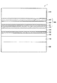
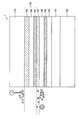
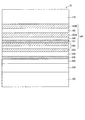
- FIG. 1 is a longitudinal sectional view schematically illustrating a main laminated structure of a magnetic tunnel junction element according to an embodiment of the present disclosure. It is a longitudinal cross-sectional view which shows typically the mode of the diffusion of the atom when performing heat processing to the magnetic tunnel junction element which concerns on the same embodiment.
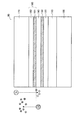
- FIG. 9 is a longitudinal sectional view schematically showing the state of diffusion of atoms when heat treatment is performed on a magnetic tunnel junction element according to a comparative example.
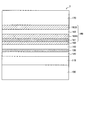
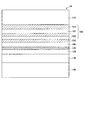
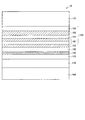
- FIG. 11 is a longitudinal sectional view schematically showing another laminated structure of the magnetic tunnel junction device according to the same embodiment.
- FIG. 11 is a longitudinal sectional view schematically showing another laminated structure of the magnetic tunnel junction device according to the same embodiment.
- FIG. 11 is a longitudinal sectional view schematically showing another laminated structure of the magnetic tunnel junction device according to the same embodiment.
- FIG. 11 is a longitudinal sectional view schematically showing another laminated structure of the magnetic tunnel junction device according to the same embodiment.
- FIG. 11 is a longitudinal sectional view schematically showing another laminated structure of the magnetic tunnel junction device according to the same embodiment.
- FIG. 11 is a longitudinal sectional view schematically showing another laminated structure of the magnetic tunnel junction device according to the same embodiment.
- FIG. 11 is a longitudinal sectional view schematically showing another laminated structure of the magnetic tunnel junction device according to the same embodiment.
- FIG. 11 is a longitudinal sectional view schematically showing another laminated structure of the magnetic tunnel junction device according to the same embodiment.
- FIG. 11 is a longitudinal sectional view schematically showing another laminated structure of the magnetic tunnel junction device according to the same embodiment.
- FIG. 11 is a longitudinal sectional view schematically showing another laminated structure of the magnetic tunnel junction device according to the same embodiment.
- FIG. 11 is a longitudinal sectional view schematically showing another laminated structure of the magnetic tunnel junction device according to the same embodiment.
- FIG. 11 is a longitudinal sectional view schematically showing another laminated structure of the magnetic tunnel junction device according to the same embodiment.
- FIG. 11 is a longitudinal sectional view schematically showing another laminated structure of the magnetic tunnel junction device according to the same embodiment.
- FIG. 11 is a longitudinal sectional view schematically showing another laminated structure of the magnetic tunnel junction device according to the same embodiment.
- FIG. 11 is a longitudinal sectional view schematically showing another laminated structure of the magnetic tunnel junction device according to the same embodiment.
- FIG. 11 is a longitudinal sectional view schematically showing another laminated structure of the magnetic tunnel junction device according to the same embodiment.
- FIG. 11 is a longitudinal sectional view schematically showing another laminated structure of the magnetic tunnel junction device according to the same embodiment.
- FIG. 11 is a longitudinal sectional view schematically showing another laminated structure of the magnetic tunnel junction device according to the same embodiment.
- FIG. 11 is a longitudinal sectional view schematically showing another laminated structure of the magnetic tunnel junction device according to the same embodiment. It is a longitudinal cross-sectional view which shows the modification of the magnetic tunnel junction element concerning the embodiment typically.
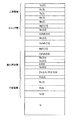
- FIG. 2 is an explanatory diagram illustrating a laminated structure of the magnetic tunnel junction device according to the first embodiment.
- FIG. 9 is an explanatory diagram illustrating a laminated structure of a magnetic tunnel junction device according to a second embodiment.
- FIG. 4 is an explanatory diagram showing a laminated structure of a magnetic tunnel junction device according to Comparative Example 1.
- FIG. 9 is an explanatory diagram illustrating a laminated structure of a magnetic tunnel junction element according to Comparative Example 2.
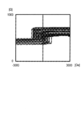
- FIG. 7 is a graph showing the evaluation results of the magneto-resistance characteristics of the magnetic tunnel junction device according to the first embodiment.
- FIG. 7 is a graph showing the evaluation results of the magneto-resistance characteristics of the magnetic tunnel junction device according to the first embodiment.
- FIG. 7 is a graph showing the evaluation results of the magneto-resistance characteristics of the magnetic tunnel junction device according to the first embodiment.
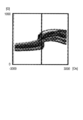
- FIG. 14 is a graph showing the evaluation results of the magneto-resistance characteristics of the magnetic tunnel junction device according to the second embodiment.
- FIG. 14 is a graph showing the evaluation results of the magneto-resistance characteristics of the magnetic tunnel junction device according to the second embodiment.
- FIG. 14 is a graph showing the evaluation results of the magneto-resistance characteristics of the magnetic tunnel junction device according to the second embodiment.
- FIG. 9 is a graph showing the evaluation results of the magneto-resistance characteristics of the magnetic tunnel junction device according to Comparative Example 1.
- FIG. 9 is a graph showing the evaluation results of the magneto-resistance characteristics of the magnetic tunnel junction device according to Comparative Example 1.
- FIG. 9 is a graph showing the evaluation results of the magneto-resistance characteristics of the magnetic tunnel junction device according to Comparative Example 1.
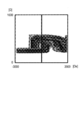
- FIG. 9 is a graph showing the evaluation results of the magneto-resistance characteristics of the magnetic tunnel junction device according to Comparative Example 2.
- FIG. 9 is a graph showing the evaluation results of the magneto-resistance characteristics of the magnetic tunnel junction device according to Comparative Example 2.
- FIG. 9 is a graph showing the evaluation results of the magneto-resistance characteristics of the magnetic tunnel junction device according to Comparative Example 2.
- FIG. 9 is an explanatory diagram illustrating a laminated structure of a magnetic tunnel junction device according to a third embodiment.
- FIG. 14 is an explanatory diagram illustrating a laminated structure of a magnetic tunnel junction device according to a fourth embodiment.
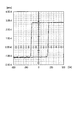
- FIG. 9 is a graph showing, as a relative value, a change in the TMR ratio of the magnetic tunnel junction element with respect to the thickness of an adjacent layer.
- FIG. 9 is a graph showing, as a relative value, a change in coercive force variation of the magnetic tunnel junction element with respect to the thickness of the barrier layer.
- FIG. 9 is a graph showing, as a relative value, a change in coercive force variation of the magnetic tunnel junction element with respect to the thickness of the intermediate layer.
- FIG. 4 is a graph showing, as a relative value, a change in coercive force of a magnetic tunnel junction element with respect to a film thickness of a magnetic layer.
- FIG. 9 is a graph showing, as a relative value, a change in a write voltage of the magnetic tunnel junction element with respect to the thickness of the magnetic layer in the adjustment layer.
- the size of some components may be exaggerated for convenience of description. Therefore, the relative sizes of the components illustrated in the drawings do not always accurately represent the magnitude relationship between the actual components.
- the direction in which the substrate and the layers are stacked is referred to as an up-down direction
- the direction in which the substrate exists is referred to as a down direction
- the direction facing the down direction is referred to as an up direction.
- FIG. 1 is a longitudinal sectional view schematically showing a main laminated structure of a magnetic tunnel junction device 1 according to the present embodiment.
- the magnetic tunnel junction device 1 has a multilayer structure including a substrate 100, a lower electrode 110, a magnetization fixed layer 120, a first insulating layer 130, a magnetization free layer 140, an adjacent layer 150, And a top layer 170 constituted by the above.
- the magnetic tunnel junction device 1 is an STT-MRAM that controls the direction of magnetization of the magnetization free layer 140 using the torque due to the spin of electrons.
- the direction of the easy axis of the magnetization free layer 140 and the magnetization fixed layer 120 is perpendicular to the film surface, so that the efficiency of magnetization reversal by spin injection can be improved. Therefore, in the magnetic tunnel junction element 1, the magnetization free layer 140 and the magnetization fixed layer 120 are caused by the interface perpendicular magnetic anisotropy induced at the interface between the magnetization fixed layer 120 and the magnetization free layer 140 and the first insulating layer 130. Perpendicular magnetic anisotropy is provided.
- An STT-MRAM such as the magnetic tunnel junction device 1 is also called an interface perpendicular magnetization type STT-MRAM.
- the substrate 100 is a member that supports each layer of the magnetic tunnel junction device 1.
- the substrate 100 may be formed of any of semiconductor, quartz, glass, and organic resin.
- the substrate 100 may be formed of a semiconductor such as silicon (Si) or germanium (Ge), or a compound semiconductor such as gallium arsenide (GaAs), gallium nitride (GaN), or silicon carbide (SiC).
- the substrate 100 may be an SOI (Silicon On Insulator) substrate in which an insulating film such as SiO 2 is sandwiched between silicon substrates.
- the lower electrode 110 is provided on the substrate 100.
- the lower electrode 110 is formed of various metal materials or alloy materials, and functions as a connection point between the magnetic tunnel junction device 1 and various wirings.
- the lower electrode 110 may be formed of a known material and a laminated structure, for example, may be formed of a single-layer film, or may be formed of a laminated film of a plurality of films. Further, the lower electrode 110 may function as a base film for controlling the crystal orientation of the magnetization fixed layer 120 provided on the lower electrode 110. In such a case, the lower electrode 110 may be formed of a metal material having substantially the same crystal structure or magnetic anisotropy as the magnetization fixed layer 120.
- the magnetization fixed layer 120 is provided on the lower electrode 110.
- the magnetization fixed layer 120 is a magnetic layer having an easy axis of magnetization perpendicular to the film surface and having a fixed magnetization direction.
- the magnetization fixed layer 120 can be formed of a known material and a laminated structure.
- the magnetization fixed layer 120 may be formed, for example, in a stacked ferrimagnetic structure in which ferromagnetic layers, nonmagnetic layers, and ferromagnetic layers are alternately stacked.
- the magnetization fixed layer 120 may be formed as a stacked film of various metal layers in order to fix the direction of magnetization, impart perpendicular magnetic anisotropy, or control the crystal structure.
- the first insulating layer 130 is provided on the magnetization fixed layer 120.
- the first insulating layer 130 functions as a tunnel insulating film of the MTJ element by being formed of an insulating material.
- the first insulating layer 130 may be formed as a thin film layer having a thickness of about 1 nm using an inorganic oxide such as magnesium oxide (MgO) or aluminum oxide (Al 2 O 3 ). More specifically, the first insulating layer 130 may be formed with magnesium oxide (MgO) to a thickness of about 1 nm.
- the first insulating layer 130 When the first insulating layer 130 is formed of magnesium oxide (MgO), the first insulating layer 130 becomes a layer having good crystallinity at a lower temperature, and thus a tunnel between the magnetization fixed layer 120 and the magnetization free layer 140 is formed.
- the magnetoresistance effect (Tunnel Magneto Resistance Effect: TMR effect) can be further enhanced.
- the magnetization free layer 140 is provided on the first insulating layer 130.
- the magnetization free layer 140 is a magnetic layer having an easy axis of magnetization in a direction perpendicular to the film surface due to interface perpendicular magnetic anisotropy generated at the interface with the first insulating layer 130 and capable of controlling the direction of magnetization.
- the magnetization free layer 140 may be formed of a magnetic material containing a 3d transition metal and boron (B), or may be formed of CoFeB with a thickness of about 1 nm to 2 nm. In such a case, by setting the content of boron (B) in the magnetization free layer 140 to 15 atomic% or more, the perpendicular magnetic anisotropy can be further enhanced.
- a magnetic tunnel junction device (MTJ device) is configured by sandwiching the first insulating layer 130 between the magnetization fixed layer 120 and the magnetization free layer 140, which are ferromagnetic materials.
- a current is caused to flow by a tunnel effect by applying a voltage perpendicularly to a junction surface between the magnetization fixed layer 120 and the magnetization free layer 140 and the first insulating layer 130.
- the magnitude of the tunnel effect changes depending on whether the magnetization directions of the magnetization fixed layer 120 and the magnetization free layer 140 are parallel or antiparallel. Therefore, the magnetic tunnel junction device 1 can control the magnitude of the current flowing between the lower electrode 110 and the upper electrode 170 by controlling the direction of magnetization of the magnetization free layer 140.
- the adjacent layer 150 is formed of a nonmagnetic transition metal and is provided adjacent to the magnetization free layer 140.
- the adjacent layer 150 suppresses the diffusion of boron (B) contained in the magnetization free layer 140 from the magnetization free layer 140 to the cap layer 160 side by heat treatment or the like.
- boron (B) contained in the magnetization free layer 140 may diffuse into a surrounding layer due to a high-temperature and long-time heat treatment. In such a case, the content of boron (B) in the magnetization free layer 140 decreases, so that it becomes difficult for the magnetization free layer 140 to maintain perpendicular magnetic anisotropy.
- the volume of the magnetization free layer 140 is limited, so that the content of boron (B) in the magnetization free layer 140 is It tends to decrease by diffusion.
- the adjacent layer 150 traps boron (B) diffused from the magnetization free layer 140, so that the boron (B) can stay around the magnetization free layer 140. According to this, the adjacent layer 150 suppresses the perpendicular magnetic anisotropy of the magnetization free layer 140 due to the decrease in the boron (B) content by suppressing the diffusion of boron (B) due to the heat treatment. can do.
- the adjacent layer 150 can be formed of a nonmagnetic transition metal having high density and high thermal conductivity.
- the adjacent layer 150 may be formed of any of molybdenum (Mo), tungsten (W), niobium (Nb), Ir (iridium), or Ti (titanium).
- the adjacent layer 150 is formed of any of molybdenum (Mo), tungsten (W), and niobium (Nb) having higher density and thermal conductivity, so that the diffusion of boron (B) is more effectively suppressed. be able to. More specifically, the adjacent layer 150 may be formed of molybdenum (Mo).
- the adjacent layer 150 may be formed with a thickness of 0.25 nm or more and 1.0 nm or less.
- the adjacent layer 150 may be a thin film that does not affect other characteristics because the diffusion of boron (B) may be suppressed to such an extent that the magnetization free layer 140 can maintain perpendicular magnetic anisotropy. It may be formed.
- the magnetic tunnel junction device 1 may have a larger TMR effect (that is, a TMR ratio) as shown in an example described later. it can.
- the cap layer 160 is formed on the adjacent layer 150.
- the cap layer 160 is provided in a multilayer structure in which a plurality of layers are stacked for the purpose of protecting the magnetization free layer 140 and the adjacent layer 150, improving the characteristics of the magnetization free layer 140, and the like.
- the cap layer 160 may be provided in a multilayer structure in which the second insulating layer 161, the intermediate layer 162, and the barrier layer 163 are sequentially stacked from the adjacent layer 150 side.
- the cap layer 160 may have a multilayer structure other than the structure illustrated in FIG. Variations of the multilayer structure of the cap layer 160 will be described later with reference to FIGS.
- the second insulating layer 161 is formed of an insulating material.
- the second insulating layer 161 may be formed as a thin film layer having a thickness of about 1 nm using an inorganic oxide such as magnesium oxide (MgO) or aluminum oxide (Al 2 O 3 ). More specifically, the second insulating layer 161 may be formed with magnesium oxide (MgO) to a thickness of about 1 nm.
- the second insulating layer 161 can control the easy axis of magnetization of the magnetization free layer 140 in a direction perpendicular to the film surface by the interface perpendicular magnetic anisotropy. Can be enhanced.
- the intermediate layer 162 is formed of a non-magnetic material.
- the intermediate layer 162 reduces a difference in crystal orientation between layers adjacent to the intermediate layer 162.
- the intermediate layer 162 may be formed of a nonmagnetic material such as Ru, Pt, Pd, TiN, or TaN with a thickness of 1 nm or more and 10 nm or less. More specifically, the intermediate layer 162 may be formed with ruthenium (Ru) to a thickness of 1 nm.
- the barrier layer 163 is formed of a non-magnetic transition metal.
- the barrier layer 163 prevents metal contained in the upper electrode 170 from diffusing into the magnetization free layer 140 or the first insulating layer 130 below the cap layer 160 due to heat treatment or the like.
- metal atoms such as tantalum (Ta) included in the upper electrode 170 diffuse into the magnetization free layer 140 or the first insulating layer 130 by the heat treatment at a high temperature and for a long time. Can occur.
- the interface between the magnetization free layer 140 and the first insulating layer 130 is disturbed by the diffused tantalum (Ta) or the like, so that the interface perpendicular magnetic anisotropy of the magnetization free layer 140 is reduced.
- the barrier layer 163 traps tantalum (Ta) or the like diffused from the upper electrode 170 to prevent the interface between the magnetization free layer 140 and the first insulating layer 130 from being disturbed by tantalum (Ta) or the like. According to this, the barrier layer 163 can prevent the perpendicular magnetic anisotropy of the magnetization free layer 140 from being reduced by the diffusion of atoms due to the heat treatment.
- the barrier layer 163 can be formed of a nonmagnetic transition metal having high density and high thermal conductivity, similarly to the adjacent layer 150.
- the barrier layer 163 may be formed of any of molybdenum (Mo), tungsten (W), niobium (Nb), Ir (iridium), or Ti (titanium).
- Mo molybdenum
- W tungsten
- Nb niobium
- Ir iridium
- Ti titanium
- the barrier layer 163 may be formed of the same nonmagnetic transition metal as the adjacent layer 150, or may be formed of a different nonmagnetic transition metal. More specifically, the barrier layer 163 may be formed of molybdenum (Mo).
- the barrier layer 163 may be formed of a metal having a larger product of the density and the thermal conductivity than the product of the density and the thermal conductivity of the metal included in the upper electrode 170.
- melting points, densities and thermal conductivities of tantalum (Ta), molybdenum (Mo), tungsten (W), niobium (Nb), Ir (iridium) and Ti (titanium) are as shown in Table 1 below. is there. Therefore, when the metal included in the upper electrode 170 is tantalum (Ta), the barrier layer 163 is made of molybdenum (Mo) having a larger product of the density and the thermal conductivity than that of the tantalum (Ta). , Iridium (Ir), or tungsten (W). In such a case, the barrier layer 163 can more effectively suppress diffusion of metal atoms from the upper electrode 170.
- the barrier layer 163 may be formed with a thickness of 1.0 nm or more and 10 nm or less. That is, the barrier layer 163 can be formed to have a larger thickness than the adjacent layer 150 formed using a similar material. According to this, the barrier layer 163 can more reliably prevent the diffusion of tantalum (Ta) from the upper electrode 170 to the magnetization free layer 140 or the first insulating layer 130.
- Ta tantalum
- the barrier layer 163 is formed with a film thickness of 1.0 nm or more as shown in an example described later, diffusion of metal from the upper electrode 170 can be sufficiently prevented. Variation can be reduced.
- the barrier layer 163 is formed with a film thickness of 10 nm or less, the workability of the magnetic tunnel junction device 1 is improved, so that a secondary characteristic variation due to the processing accuracy or the like can be reduced.
- the upper electrode 170 is provided on the cap layer 160.
- the upper electrode 170 is formed of various metal materials or alloy materials, and functions as a connection point between the magnetic tunnel junction device 1 and various wirings.
- the upper electrode 170 may be formed of a known material and a laminated structure, for example, may be formed of a single-layer film, or may be formed of a laminated film of a plurality of films. Further, the upper electrode 170 may function as a hard mask when the magnetic tunnel junction element 1 is processed by etching or the like. In such a case, the upper electrode 170 may be formed to include tantalum (Ta) or tantalum nitride (TaN).
- the upper electrode 170 has a multilayer structure in which a Ru film having a thickness of 1 nm, a Ta film having a thickness of 1 nm, a Ru film having a thickness of 5 nm, and a Ta film having a thickness of 77 nm are sequentially stacked from the cap layer 160 side. May be formed.
- the upper electrode 170 has a multilayer structure in which a Ru film having a thickness of 1 nm, a Ta film having a thickness of 1 nm, a Ru film having a thickness of 5 nm, and a TaN film having a thickness of 77 nm are sequentially stacked from the cap layer 160 side.
- the adjacent layer 150 formed of the nonmagnetic transition metal is provided adjacent to the magnetization free layer 140, and similarly formed of the nonmagnetic transition metal.
- the barrier layer 163 is provided in the cap layer 160.
- FIG. 2A is a vertical cross-sectional view schematically showing the state of diffusion of atoms when heat treatment is performed on the magnetic tunnel junction device 1 according to the present embodiment.
- FIG. 2B is a vertical cross-sectional view schematically illustrating the state of diffusion of atoms when heat treatment is performed on the magnetic tunnel junction element 90 according to the comparative example.
- the adjacent layer 150 and the barrier layer 163 are not provided as compared with the magnetic tunnel junction device 1. Therefore, in the magnetic tunnel junction element 90 according to the comparative example, when heat treatment is performed at high temperature and for a long time, metal atoms such as tantalum (Ta) included in the upper electrode 170 diffuse to the cap layer 160 side. I will.
- the tantalum (Ta) diffused by the heat treatment disturbs the interface between the magnetization free layer 140 and the first insulating layer 130, and lowers the perpendicular magnetic anisotropy of the interface. Let me do it.
- the perpendicular magnetic anisotropy of the magnetization free layer 140 is reduced by the high-temperature and long-time heat treatment.
- the magnetic tunnel junction device 1 when heat treatment is performed at high temperature and for a long time, metal atoms such as tantalum (Ta) included in the upper electrode 170 are: The diffusion to the cap layer 160 side is prevented by the barrier layer 163. As a result, in the magnetic tunnel junction device 1 according to the present embodiment, the interface between the magnetization free layer 140 and the first insulating layer 130 is not disturbed by tantalum (Ta) or the like. Can be maintained. Further, diffusion of boron (B) contained in the magnetization free layer 140 to the cap layer 160 side by the adjacent layer 150 is suppressed. Therefore, the magnetization free layer 140 can hold a sufficient amount of boron (B) to maintain perpendicular magnetic anisotropy.
- Ta tantalum
- the reduction of the perpendicular magnetic anisotropy of the magnetization free layer 140 can be suppressed by suppressing the diffusion of atoms generated by the high-temperature and long-time heat treatment. .
- the magnetic tunnel junction device 1 according to the present embodiment can maintain desired magnetic characteristics even when a high-load heat treatment is performed. Therefore, the magnetic tunnel junction element 1 according to the present embodiment restricts a manufacturing process for a semiconductor device in which various circuits such as a logic circuit, a memory circuit, and a pixel circuit are mounted and various heat treatment processes are performed. Can be loaded together.
- FIGS. 3 to 18 are longitudinal sectional views schematically showing other laminated structures of the magnetic tunnel junction devices 2 to 17 according to the present embodiment.
- the magnetic tunnel junction device 2 is different from the magnetic tunnel junction device 1 shown in FIG. 1 in that the stacking order of the intermediate layer 162 and the barrier layer 163 is changed.
- the cap layer 160 of the magnetic tunnel junction device 2 has a structure in which the second insulating layer 161, the barrier layer 163, and the intermediate layer 162 are stacked from the adjacent layer 150 side. That is, the barrier layer 163 does not need to be provided adjacent to the upper electrode 170 and may be provided at any position of the cap layer 160.
- barrier layer 163 is a layer that prevents diffusion of metal from the upper electrode 170 to the interface between the magnetization free layer 140 and the first insulating layer 130, any one of the barrier layers 163 between the upper electrode 170 and the adjacent layer 150 What is necessary is just to be provided in the position.
- the cap layer 160 includes the second insulating layer 161
- the second insulating layer 161 is adjacent to the adjacent layer 150 in order to increase the perpendicular magnetic anisotropy of the magnetization free layer 140 by the interface perpendicular magnetic anisotropy.
- the barrier layer 163 is provided at any position between the upper electrode 170 and the second insulating layer 161.
- the magnetic tunnel junction device 3 is different from the magnetic tunnel junction device 1 shown in FIG. 1 in that a plurality of barrier layers 163A and 163B are provided.
- the cap layer 160 of the magnetic tunnel junction device 3 has a structure in which the second insulating layer 161, the first barrier layer 163A, the intermediate layer 162, and the second barrier layer 163B are stacked from the adjacent layer 150 side. Prepare.
- the first barrier layer 163A and the second barrier layer 163B are formed of the same material and thickness as the barrier layer 163 of the magnetic tunnel junction device 1 shown in FIG. Prevent spread.
- the magnetic tunnel junction device 3 shown in FIG. 4 since a plurality of barrier layers 163A and 163B are provided, the diffusion of tantalum (Ta) or the like from the upper electrode 170 during the heat treatment is more reliably prevented, so that the magnetization is improved. The lowering of the perpendicular magnetic anisotropy of the free layer 140 can be more reliably prevented.
- the magnetic tunnel junction device 4 is different from the magnetic tunnel junction device 1 shown in FIG. 1 in that a magnetic layer 164 is inserted between the second insulating layer 161 and the intermediate layer 162. .
- the cap layer 160 of the magnetic tunnel junction device 4 has a structure in which the second insulating layer 161, the magnetic layer 164, the intermediate layer 162, and the barrier layer 163 are stacked from the adjacent layer 150 side.
- the magnetic layer 164 is made of a magnetic material containing a 3d transition metal and boron (B), similarly to the magnetization free layer 140, and improves the magnetic characteristics of the magnetic tunnel junction device 4. Specifically, the magnetic layer 164 is stacked adjacent to the second insulating layer 161 to improve the crystallinity of the second insulating layer 161 after the heat treatment. Thereby, the magnetic layer 164 can improve the perpendicular magnetic anisotropy of the magnetization free layer 140 via the adjacent layer 150.
- B 3d transition metal and boron
- the magnetic layer 164 may be formed of CoFeB with a thickness of 0.9 nm or less.
- the perpendicular magnetic anisotropy of the magnetic layer 164 can be further enhanced by setting the content of boron (B) to 15 atomic% or more.
- the magnetic tunnel junction element 4 has a high perpendicular magnetic anisotropy by forming the magnetic layer 164 provided on the second insulating layer 161 with a thickness of 0.9 nm or less. Properties and coercive forces.
- the lower limit of the thickness of the magnetic layer 164 is not particularly limited, but may be 0.1 nm. In the magnetic tunnel junction device 4 shown in FIG. 5, since the magnetic layer 164 is provided in addition to the magnetization free layer 140, the magnetic characteristics of the entire magnetic tunnel junction device 4 can be improved.
- the magnetic tunnel junction device 5 is different from the magnetic tunnel junction device 4 shown in FIG. 5 in that the stacking order of the intermediate layer 162 and the barrier layer 163 is changed.
- the cap layer 160 of the magnetic tunnel junction device 5 has a structure in which the second insulating layer 161, the magnetic layer 164, the barrier layer 163, and the intermediate layer 162 are stacked from the adjacent layer 150 side. That is, the barrier layer 163 does not need to be provided adjacent to the upper electrode 170 and may be provided at any position of the cap layer 160. Since the barrier layer 163 is a layer that prevents diffusion of metal from the upper electrode 170, it may be provided at any position between the upper electrode 170 and the magnetic layer 164.
- the magnetic tunnel junction device 6 is different from the magnetic tunnel junction device 3 shown in FIG. 4 in that a plurality of barrier layers 163A and 163B are provided.
- the cap layer 160 of the magnetic tunnel junction device 6 includes the second insulating layer 161, the magnetic layer 164, the first barrier layer 163A, the intermediate layer 162, and the second barrier layer 163B from the adjacent layer 150 side. It has a laminated structure.
- the first barrier layer 163A and the second barrier layer 163B are formed of the same material and thickness as the barrier layer 163 of the magnetic tunnel junction device 1 shown in FIG. Prevent spread. Further, the first barrier layer 163A can suppress the diffusion of boron (B) from the magnetic layer 164. In the magnetic tunnel junction device 6 shown in FIG. 7, since a plurality of barrier layers 163A and 163B are provided, diffusion of tantalum (Ta) or the like from the upper electrode 170 during heat treatment is more reliably prevented, and the magnetization free layer is formed. The lowering of the perpendicular magnetic anisotropy of the magnetic layer 140 and the magnetic layer 164 can be prevented more reliably.
- the magnetic tunnel junction element 7 is different from the magnetic tunnel junction element 1 shown in FIG. 1 in that the second insulating layer 161 is not provided and each layer of the cap layer 160 is formed of a conductive material.
- the cap layer 160 of the magnetic tunnel junction device 7 has a structure in which the intermediate layer 162 and the barrier layer 163 are stacked from the adjacent layer 150 side.
- the second insulating layer 161 is a layer that increases the perpendicular magnetic anisotropy of the magnetization free layer 140 by the interface perpendicular magnetic anisotropy. Good.
- the manufacturing cost can be reduced by simplifying the laminated structure of the cap layer 160.
- the magnetic tunnel junction device 8 includes a 3d transition metal and boron (B) between the second insulating layer 161 and the intermediate layer 162 with respect to the magnetic tunnel junction device 1 shown in FIG. The difference is that an adjustment layer 165 in which a magnetic layer formed of a magnetic material and a nonmagnetic layer formed of a nonmagnetic transition metal are stacked is inserted. More specifically, the cap layer 160 of the magnetic tunnel junction device 8 is formed by laminating an adjustment layer 165 composed of a magnetic layer and a nonmagnetic layer, a second insulating layer 161, an intermediate layer 162, and a barrier layer 163 from the adjacent layer 150 side. With structure.
- the magnetic layer of the adjustment layer 165 is formed of a magnetic material containing a 3d transition metal and boron (B), similarly to the magnetization free layer 140, and may be formed of, for example, CoFeB to a thickness of 0.7 nm or less. .
- the perpendicular magnetic anisotropy of the magnetic layer of the adjustment layer 165 can be further enhanced by setting the content of boron (B) to 15 atomic% or more.
- the magnetic layer of the adjustment layer 165 is formed to have a thickness of 0.7 nm or less, so that an excessively high write voltage can be prevented.
- the lower limit of the thickness of the magnetic layer of the adjustment layer 165 is not particularly limited, but may be 0.1 nm.
- the nonmagnetic layer of the adjustment layer 165 is formed of a nonmagnetic transition metal such as molybdenum (Mo), tungsten (W), niobium (Nb), Ir (iridium), or Ti (titanium), like the adjacent layer 150.
- a nonmagnetic transition metal such as molybdenum (Mo), tungsten (W), niobium (Nb), Ir (iridium), or Ti (titanium), like the adjacent layer 150.
- Mo molybdenum
- tungsten W
- Nb niobium
- Ir iridium
- Ti titanium
- the cap layer 160 includes the adjustment layer 165 having the same laminated structure as the magnetization free layer 140 and the adjacent layer 150, so that the boron (B) near the magnetization free layer 140 after the heat treatment is formed. ) Can be controlled with higher accuracy. According to this, the magnetic tunnel junction element 8 can more reliably prevent the perpendicular anisotropy of the magnetization free layer 140 from decreasing due to the heat treatment.
- the magnetic tunnel junction element 9 shown in FIG. 10 is different from the magnetic tunnel junction element 8 shown in FIG. 9 in that the stacking order of the intermediate layer 162 and the barrier layer 163 is changed.
- the cap layer 160 of the magnetic tunnel junction device 9 has the adjustment layer 165 composed of a magnetic layer and a non-magnetic layer, the second insulating layer 161, the barrier layer 163, and the intermediate layer 162 stacked from the adjacent layer 150 side.
- the barrier layer 163 does not need to be provided adjacent to the upper electrode 170 and may be provided at any position of the cap layer 160.
- the barrier layer 163 is a layer that prevents diffusion of metal from the upper electrode 170 to the interface between the magnetization free layer 140 and the first insulating layer 130, any one of the barrier layers 163 between the upper electrode 170 and the second insulating layer 161. It may be provided at such a position.
- the magnetic tunnel junction device 10 is different from the magnetic tunnel junction device 8 shown in FIG. 9 in that a plurality of barrier layers 163A and 163B are provided. More specifically, the cap layer 160 of the magnetic tunnel junction device 10 includes an adjustment layer 165 composed of a magnetic layer and a nonmagnetic layer, a second insulating layer 161, a first barrier layer 163A, an intermediate layer 162, and a second barrier layer. It has a structure in which the layer 163B is stacked.
- the first barrier layer 163A and the second barrier layer 163B are formed of the same material and thickness as the barrier layer 163 of the magnetic tunnel junction device 1 shown in FIG. Prevent spread.
- the magnetic tunnel junction device 10 shown in FIG. 11 since a plurality of barrier layers 163A and 163B are provided, diffusion of tantalum (Ta) or the like from the upper electrode 170 during heat treatment is more reliably prevented, and the magnetization free layer is formed. 140 can be more reliably prevented from decreasing.
- the magnetic tunnel junction device 11 is different from the magnetic tunnel junction device 8 shown in FIG. 9 in that a magnetic layer 164 is inserted between the second insulating layer 161 and the intermediate layer 162.
- the cap layer 160 of the magnetic tunnel junction device 11 includes an adjustment layer 165 composed of a magnetic layer and a nonmagnetic layer, a second insulating layer 161, a magnetic layer 164, an intermediate layer 162, and a barrier layer from the adjacent layer 150 side. 163 is provided.
- the magnetic layer 164 is formed of a magnetic material containing a 3d transition metal and boron (B), similarly to the magnetization free layer 140, and improves the magnetic characteristics of the magnetic tunnel junction device 11. Specifically, the magnetic layer 164 is stacked adjacent to the second insulating layer 161 to improve the crystallinity of the second insulating layer 161 after the heat treatment. Thereby, the magnetic layer 164 can improve the perpendicular magnetic anisotropy of the magnetization free layer 140 via the adjacent layer 150.
- B 3d transition metal and boron
- the magnetic layer 164 may be formed of CoFeB with a thickness of 0.9 nm or less.
- the perpendicular magnetic anisotropy of the magnetic layer 164 can be further enhanced by setting the content of boron (B) to 15 atomic% or more.
- the magnetic tunnel junction element 11 has a high perpendicular magnetic anisotropy by forming the magnetic layer 164 provided on the second insulating layer 161 to a thickness of 0.9 nm or less. Properties and coercive forces.
- the lower limit of the thickness of the magnetic layer 164 is not particularly limited, but may be 0.1 nm. In the magnetic tunnel junction device 11 shown in FIG. 12, since the magnetic layer 164 is provided in addition to the magnetization free layer 140, the magnetic characteristics of the entire magnetic tunnel junction device 11 can be improved.
- the magnetic tunnel junction element 12 is different from the magnetic tunnel junction element 11 shown in FIG. 12 in that the stacking order of the intermediate layer 162 and the barrier layer 163 is changed.
- the cap layer 160 of the magnetic tunnel junction device 12 includes an adjustment layer 165 composed of a magnetic layer and a non-magnetic layer, a second insulating layer 161, a magnetic layer 164, a barrier layer 163, and an intermediate layer from the adjacent layer 150 side. 162 are laminated. That is, the barrier layer 163 does not need to be provided adjacent to the upper electrode 170 and may be provided at any position of the cap layer 160. Since the barrier layer 163 is a layer that prevents diffusion of metal from the upper electrode 170, it may be provided at any position between the upper electrode 170 and the magnetic layer 164.
- the magnetic tunnel junction device 13 is different from the magnetic tunnel junction device 11 shown in FIG. 12 in that a plurality of barrier layers 163A and 163B are provided.
- the cap layer 160 of the magnetic tunnel junction device 13 includes an adjustment layer 165 composed of a magnetic layer and a nonmagnetic layer, a second insulating layer 161, a magnetic layer 164, a first barrier layer 163A, It has a structure in which an intermediate layer 162 and a second barrier layer 163B are stacked.
- the first barrier layer 163A and the second barrier layer 163B are formed of the same material and thickness as the barrier layer 163 of the magnetic tunnel junction device 1 shown in FIG. Prevent spread. Further, the first barrier layer 163A can suppress the diffusion of boron (B) from the magnetic layer 164. In the magnetic tunnel junction element 13 shown in FIG. 14, since a plurality of barrier layers 163A and 163B are provided, diffusion of tantalum (Ta) or the like from the upper electrode 170 during heat treatment is more reliably prevented, and the magnetization free layer is formed. The lowering of the perpendicular magnetic anisotropy of the magnetic layer 140 and the magnetic layer 164 can be prevented more reliably.
- the magnetic tunnel junction device 14 is different from the magnetic tunnel junction device 8 shown in FIG. 9 in that the second insulating layer 161 is not provided and each layer of the cap layer 160 is formed of a conductive material.
- the cap layer 160 of the magnetic tunnel junction device 14 has a structure in which an adjustment layer 165 composed of a magnetic layer and a nonmagnetic layer, an intermediate layer 162, and a barrier layer 163 are stacked from the adjacent layer 150 side.
- the second insulating layer 161 is a layer that enhances the perpendicular magnetic anisotropy of the magnetization free layer 140 due to the interface perpendicular magnetic anisotropy, and therefore cannot be provided depending on the degree of the perpendicular magnetic anisotropy of the magnetization free layer 140. May be.
- the manufacturing cost can be reduced by simplifying the laminated structure of the cap layer 160.
- the magnetic tunnel junction device 15 is different from the magnetic tunnel junction device 14 shown in FIG. 15 in that a magnetic layer 164 is inserted between the adjustment layer 165 and the intermediate layer 162.
- the cap layer 160 of the magnetic tunnel junction device 15 has a structure in which an adjustment layer 165 composed of a magnetic layer and a nonmagnetic layer, a magnetic layer 164, an intermediate layer 162, and a barrier layer 163 are stacked from the adjacent layer 150 side. Prepare.
- the magnetic layer 164 may be formed of a magnetic material containing a 3d transition metal and boron (B), or may be formed of CoFeB with a thickness of 0.9 nm or less.
- the perpendicular magnetic anisotropy of the magnetic layer 164 can be further enhanced by setting the content of boron (B) to 15 atomic% or more.
- the magnetic tunnel junction device 15 can have high perpendicular magnetic anisotropy and coercive force.
- the lower limit of the thickness of the magnetic layer 164 is not particularly limited, but may be 0.1 nm. In the magnetic tunnel junction device 15 shown in FIG. 16, since the magnetic layer 164 is provided in addition to the magnetization free layer 140, the magnetic characteristics of the entire magnetic tunnel junction device 15 can be improved.
- the magnetic tunnel junction element 16 is different from the magnetic tunnel junction element 15 shown in FIG. 16 in that the stacking order of the intermediate layer 162 and the barrier layer 163 is changed.
- the cap layer 160 of the magnetic tunnel junction device 16 has a structure in which an adjustment layer 165 composed of a magnetic layer and a nonmagnetic layer, a magnetic layer 164, a barrier layer 163, and an intermediate layer 162 are stacked from the adjacent layer 150 side.
- the barrier layer 163 does not need to be provided adjacent to the upper electrode 170 and may be provided at any position of the cap layer 160. Since the barrier layer 163 is a layer that prevents diffusion of metal from the upper electrode 170, it may be provided at any position between the upper electrode 170 and the magnetic layer 164.
- the magnetic tunnel junction device 17 is different from the magnetic tunnel junction device 15 shown in FIG. 16 in that a plurality of barrier layers 163A and 163B are provided.
- the cap layer 160 of the magnetic tunnel junction device 17 includes the adjustment layer 165 composed of a magnetic layer and a nonmagnetic layer, the magnetic layer 164, the first barrier layer 163A, the intermediate layer 162, and the It has a structure in which two barrier layers 163B are stacked.
- the first barrier layer 163A and the second barrier layer 163B are formed of the same material and thickness as the barrier layer 163 of the magnetic tunnel junction device 1 shown in FIG. Prevent spread. Further, the first barrier layer 163A can suppress the diffusion of boron (B) from the magnetic layer 164. In the magnetic tunnel junction element 17 shown in FIG. 18, since a plurality of barrier layers 163A and 163B are provided, diffusion of tantalum (Ta) or the like from the upper electrode 170 during heat treatment is more reliably prevented, and the magnetization free layer is formed. The lowering of the perpendicular magnetic anisotropy of the magnetic layer 140 and the magnetic layer 164 can be prevented more reliably.
- Each of the layers constituting the magnetic tunnel junction elements 1 to 17 according to the present embodiment can be formed by a sputtering method.
- the film forming conditions and the like of the sputtering method are not particularly limited, and optimal conditions can be appropriately selected.
- FIG. 19 is a longitudinal sectional view schematically showing a magnetic tunnel junction device 1 according to this modification.
- the magnetic tunnel junction device 1 according to the present modification is processed by etching or the like, and the exposed surface after the device processing is covered with the protective film 180.
- the protective film 180 only needs to cover at least the side surfaces of the magnetic tunnel junction device 1, and does not necessarily have to cover the upper surface of the magnetic tunnel junction device 1.
- the protective film 180 is an insulating film such as SiN x or SiO x and can be formed by a physical film forming method such as PVD (Physical Vapor Deposition).
- the protective film 180 may be a SiN film formed by plasma PVD.
- the end surfaces of the magnetization free layer 140 and the magnetization fixed layer 120 are exposed. Therefore, when these end faces are exposed to a source gas (for example, SiH 4 or NH 3 ) used in a chemical deposition method such as CVD (Chemical Vapor Deposition), the magnetization free layer 140 and the magnetization There is a possibility that the magnetic properties of the fixed layer 120 may be degraded. Therefore, by forming the protective film 180 by a physical film forming method, it is possible to prevent the magnetic characteristics of the magnetic tunnel junction device 1 after the device processing from being deteriorated.
- a source gas for example, SiH 4 or NH 3
- CVD Chemical Vapor Deposition
- the thickness of the protective film 180 is not particularly limited, but may be, for example, 5 nm or more and 30 nm or less.
- the protective film 180 can be formed by performing reactive sputtering in an Ar and N 2 gas atmosphere using a silicon (Si) target having a purity of more than 5N, for example.
- the flow rates of the Ar gas and the N 2 gas may be, for example, 20 sccm, respectively.
- the write voltage can be further reduced in the magnetic tunnel junction device 1 whose side surface is protected by the protective film 180 formed by such a physical film forming method.
- the writing voltage tends to increase due to the thermal load. Therefore, it is more preferable to reduce the writing voltage by using the protective film 180 described above. .
- the magnetic tunnel junction device according to the present embodiment will be specifically described with reference to examples and comparative examples.
- the following example is merely an example, and the magnetic tunnel junction device according to the present embodiment is not limited to the following example.
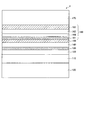
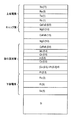
- FIG. 20 is an explanatory diagram illustrating a stacked structure of the magnetic tunnel junction device according to the first embodiment.
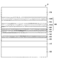
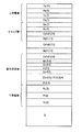
- FIG. 21 is an explanatory diagram illustrating a stacked structure of the magnetic tunnel junction device according to the second embodiment.
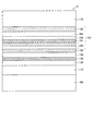
- FIG. 22 is an explanatory diagram illustrating a stacked structure of the magnetic tunnel junction element according to Comparative Example 1.
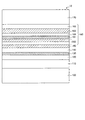
- FIG. 23 is an explanatory diagram illustrating a stacked structure of the magnetic tunnel junction device according to Comparative Example 2. 20 to 23, the numerical values in parentheses indicate the thickness of each layer in units of nanometers.
- a lower electrode made of Ta (5 nm), Pt (5 nm) and Ru (3 nm), Pt (0.3 nm), Co (0.5 nm) and Pt (0. 3 nm), a magnetization fixed layer made of Co (0.5 nm), Ir (0.5 nm), Co (0.6 nm), Mo (0.4 nm), CoFeB (0.9 nm), and MgO. (1.0 nm) first insulating layer, CoFeB (1.5 nm) free magnetization layer, Mo (0.8 nm) adjacent layer, MgO (1.0 nm), Ru (7 nm) and Mo (7 nm). ) And an upper electrode made of Ru (1 nm), Ta (1 nm), Ru (5 nm), and Ta (77 nm), thereby manufacturing a magnetic tunnel junction device according to Example 1. .
- a lower electrode made of Ta (5 nm), Pt (5 nm) and Ru (3 nm), a Pt (0.3 nm), Co (0.5 nm) and Pt ( 0.3 nm), a magnetization fixed layer made of Co (0.5 nm), Ir (0.5 nm), Co (0.6 nm), Mo (0.4 nm), and CoFeB (0.9 nm).
- MgO 1.0 nm
- a magnetization free layer of CoFeB 1.5 nm
- an adjacent layer of Mo 0.8 nm
- CoFeB 0.5 nm
- Mo 0.8 nm
- MgO 1.0 nm
- the magnetic tunnel junction device according to Example 2 was manufactured. It was.
- Ta (1 nm), Ru (5 nm), and an upper electrode made of Ta (77 nm) were laminated to produce a magnetic tunnel junction device according to Comparative Example 1.
- a lower electrode made of Ta (5 nm), Pt (5 nm) and Ru (3 nm), a Pt (0.3 nm), Co (0.5 nm) and Pt ( 0.3 nm), a magnetization fixed layer made of Co (0.5 nm), Ir (0.5 nm), Co (0.6 nm), Mo (0.4 nm), and CoFeB (0.9 nm).
- MgO 1.0 nm
- CoFeB 1.5 nm
- a magnetic tunnel junction device according to Comparative Example 2 was manufactured by laminating a cap layer made of and an upper electrode made of Ru (1 nm), Ta (1 nm), Ru (5 nm), and Ta (77 nm).
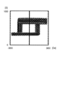
- FIGS. 24A to 24C are graphs showing evaluation results of the magneto-resistance characteristics of the magnetic tunnel junction device according to Example 1.
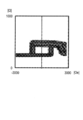
- FIG. 25A to 25C are graphs showing the evaluation results of the magneto-resistance characteristics of the magnetic tunnel junction device according to Example 2.
- 26A to 26C are graphs showing evaluation results of the magneto-resistance characteristics of the magnetic tunnel junction device according to Comparative Example 1.
- 27A to 27C are graphs showing evaluation results of the magneto-resistance characteristics of the magnetic tunnel junction device according to Comparative Example 2.
- Example 1 in the magnetic tunnel junction device according to Example 1, a film is formed on a Si substrate (FIG. 24A), a device is processed (FIG. 24B), and a heat treatment is performed (FIG. 24C), a square hysteresis curve is formed. Therefore, in Example 1, it can be seen that the magnetic tunnel junction element functions as an MTJ element even after element processing and heat treatment, and the magnetization free layer retains perpendicular magnetic anisotropy.
- Example 2 in the magnetic tunnel junction device according to Example 2, a film is formed on a Si substrate (FIG. 25A), a device is processed (FIG. 25B), and a heat treatment is performed (FIG. 25C), a square hysteresis curve is formed. Therefore, in Example 2, it can be seen that the magnetic tunnel junction element functions as an MTJ element even after element processing and heat treatment, and the magnetization free layer retains perpendicular magnetic anisotropy.
- FIGS. 27A to 27C in the magnetic tunnel junction device according to Comparative Example 2, a square hysteresis curve is shown in a state where a film is formed on a Si substrate (FIG. 27A) and a state where the element is processed (FIG. 27B). Although it is formed, it can be seen that no hysteresis curve is formed in the heat-treated state (FIG. 27C). Therefore, in Comparative Example 2, although the magnetization free layer has perpendicular magnetic anisotropy when formed on a Si substrate and when a device is processed, the magnetization free layer loses perpendicular magnetic anisotropy by heat treatment. It can be seen that the magnetic tunnel junction element of No. does not function as an MTJ element.
- the adjacent layer formed of the nonmagnetic transition metal is provided adjacent to the magnetization free layer, and the barrier layer similarly formed of the nonmagnetic transition metal is formed of the cap layer. It can be seen that the element functions as an MTJ element even after element processing and heat treatment. That is, it can be seen that the magnetic tunnel junction element according to the present embodiment has improved resistance to heat treatment.
- FIG. 30 shows a change in the TMR ratio of the magnetic tunnel junction device when the thickness of the adjacent layer of the magnetic tunnel junction device according to the first embodiment is changed from 0.15 nm to 1.15 nm.
- FIG. 30 is a graph showing, as a relative value, a change in the TMR ratio of the magnetic tunnel junction element with respect to the film thickness of the adjacent layer (Mo). Referring to FIG. 30, it is found that when the thickness of the adjacent layer (Mo) is 0.1 nm or more and 1 nm or less, the TMR ratio of the magnetic tunnel junction device is further improved.
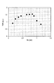
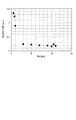
- FIG. 31 shows a change in coercive force (Hc) variation of the magnetic tunnel junction device when the thickness of the barrier layer of the magnetic tunnel junction device according to the first embodiment is changed from 0.5 nm to 11 nm.
- FIG. 31 is a graph showing, as a relative value, a change in variation in coercive force (Hc) of the magnetic tunnel junction element with respect to the thickness of the barrier layer (Mo). Referring to FIG. 31, it can be seen that when the thickness of the barrier layer (Mo) is 1 nm or more, the coercive force (Hc) variation of the magnetic tunnel junction element becomes smaller. On the other hand, when the thickness of the barrier layer is 10 nm or less, the processing of the magnetic tunnel junction element is facilitated, so that the processing accuracy of the magnetic tunnel junction element can be improved.
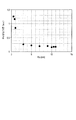
- FIG. 32 shows a change in coercive force (Hc) variation of the magnetic tunnel junction device when the thickness of the intermediate layer of the magnetic tunnel junction device according to the first embodiment is changed from 0.5 nm to 11 nm.
- FIG. 32 is a graph showing, as a relative value, a change in variation in coercive force (Hc) of the magnetic tunnel junction element with respect to the thickness of the intermediate layer (Ru). Referring to FIG. 32, it is found that when the thickness of the intermediate layer is 1 nm or more, the coercive force (Hc) variation of the magnetic tunnel junction element is reduced. On the other hand, when the thickness of the intermediate layer is 10 nm or less, the processing of the magnetic tunnel junction element is facilitated, so that the processing accuracy of the magnetic tunnel junction element can be improved.
- FIG. 28 is an explanatory diagram illustrating the stacked structure of the magnetic tunnel junction device according to the third embodiment.
- a lower electrode made of Ta (5 nm), Pt (5 nm) and Ru (3 nm), Pt (0.3 nm), Co (0.5 nm) and Pt (0. 3 nm), a magnetization fixed layer made of Co (0.5 nm), Ir (0.5 nm), Co (0.6 nm), Mo (0.4 nm), CoFeB (0.9 nm), and MgO.
- FIG. 33 shows a change in the coercive force (Hc) of the magnetic tunnel junction device when the thickness of the magnetic layer of the magnetic tunnel junction device according to the third embodiment was changed from 0 nm to 3.5 nm.
- FIG. 33 is a graph showing, as a relative value, a change in the coercive force (Hc) of the magnetic tunnel junction element with respect to the thickness of the magnetic layer (CoFeB). Referring to FIG. 33, it can be seen that when the thickness of the magnetic layer (CoFeB) is 0.9 nm or less, the coercive force (Hc) of the magnetic tunnel junction element becomes larger.
- FIG. 29 is an explanatory diagram illustrating the stacked structure of the magnetic tunnel junction device according to the fourth embodiment.
- a lower electrode made of Ta (5 nm), Pt (5 nm) and Ru (3 nm), and Pt (0.3 nm), Co (0.5 nm) and Pt (0. 3 nm), a magnetization fixed layer made of Co (0.5 nm), Ir (0.5 nm), Co (0.6 nm), Mo (0.4 nm), CoFeB (0.9 nm), and MgO. (1.0 nm) first insulating layer, CoFeB (1.5 nm) magnetization free layer, Mo (0.8 nm) adjacent layer, and adjustment of CoFeB (0 nm to 1 nm) and Mo (0.8 nm).
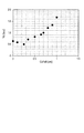
- FIG. 34 shows a change in the write voltage (Vc) of the magnetic tunnel junction element when the thickness of the magnetic layer in the adjustment layer of the magnetic tunnel junction element according to Example 4 was changed from 0 nm to 1 nm.
- FIG. 34 is a graph showing, as a relative value, a change in the write voltage (Vc) of the magnetic tunnel junction element with respect to the thickness of the magnetic layer (CoFeB) in the adjustment layer. Referring to FIG. 34, it can be seen that when the thickness of the magnetic layer (CoFeB) in the adjustment layer is 0.7 nm or less, the write voltage of the magnetic tunnel junction device can be further reduced.
- the magnetic tunnel junction elements 1 to 17 can be mounted together with transistors and the like on various semiconductor devices.
- the magnetic tunnel junction elements 1 to 17 may be mounted on a semiconductor device such as a solid-state imaging device, an arithmetic processing device, a communication device, or a storage device.
- a magnetic tunnel junction device comprising: (2) Further comprising an upper electrode provided on the cap layer, The magnetic tunnel junction device according to (1), wherein the product of the density and the thermal conductivity of the nonmagnetic transition metal is higher than the product of the density and the thermal conductivity of the metal material included in the upper electrode.
- the upper electrode includes Ta or TaN, The magnetic tunnel junction device according to (2), wherein the metal material included in the upper electrode is Ta.
- the cap layer further includes a stacked structure in which a layer formed of the nonmagnetic transition metal is stacked on a magnetic layer formed of a magnetic material including a 3d transition metal and B, The magnetic tunnel junction device according to any one of (1) to (4), wherein the laminated structure is provided such that the magnetic layer is adjacent to the adjacent layer.
- the cap layer further includes a second insulating layer formed of an insulating material.
- the magnetic tunnel junction device according to any one of (1) to (14), wherein the thickness of the adjacent layer is 0.25 nm or more and 1 nm or less.
- the cap layer further includes an intermediate layer formed of a non-magnetic material, The magnetic tunnel junction device according to any one of (1) to (16), wherein a thickness of the intermediate layer is 1 nm or more and 10 nm or less.
- the magnetic tunnel junction device according to any one of (1) to (17), wherein the magnetic tunnel junction device has a columnar shape or a cone shape.
- a magnetic tunnel junction element The magnetic tunnel junction element, A magnetization fixed layer having a fixed magnetization direction, A first insulating layer provided on the magnetization fixed layer and formed of an insulating material; A magnetization free layer provided on the first insulating layer; An adjacent layer provided adjacent to the magnetization free layer and formed of a nonmagnetic transition metal; A cap layer formed in a multilayer structure including at least one or more barrier layers formed of the nonmagnetic transition metal, and provided on the adjacent layer;
- a semiconductor device comprising:
Landscapes
- Hall/Mr Elements (AREA)
- Mram Or Spin Memory Techniques (AREA)
- Superconductor Devices And Manufacturing Methods Thereof (AREA)
Abstract
磁化の向きが固定された磁化固定層(120)と、前記磁化固定層の上に設けられ、絶縁材料で形成された第1絶縁層(130)と、前記第1絶縁層の上に設けられた磁化自由層(140)と、前記磁化自由層の上に隣接して設けられ、非磁性遷移金属で形成された隣接層(150)と、前記非磁性遷移金属で形成されたバリア層(163)を少なくとも1つ以上含む多層構造で形成され、前記隣接層の上に設けられたキャップ層(160)と、を備える、磁気トンネル接合素子(1)。
Description
本開示は、磁気トンネル接合素子及び半導体装置に関する。
近年、半導体装置では、CMOS(Complementary MOS)を用いたロジック回路に大容量の不揮発メモリを混載させることが一般的になっている。
例えば、ロジック回路にSRAM(Static Random Access Memory)等を混載させることが行われている。一方で、半導体装置のコスト及び消費電力を低減するために、SRAMを磁気抵抗メモリ(Magnetoresistive Random Access Memory:MRAM)で置換することが検討されている。
磁気抵抗メモリ(MRAM)は、絶縁性薄膜を一対の強磁性層で挟持した磁気トンネル接合(Magnetic Tunnel Junction:MTJ)素子を利用したメモリ素子である。MTJ素子では、一対の強磁性層の相対的な磁化の向きによってトンネル抵抗の大きさが変化する。これにより、MTJ素子は、一対の強磁性層の磁化の向きを平行又は反平行のいずれかに制御することで、情報を記憶することができる。
例えば、下記の特許文献1には、MTJ素子を用いた界面垂直磁化型のSTT-MRAM(Spin Transfer Torque-MRAM)が開示されている。特許文献1には、配線形成プロセスにおける熱負荷に耐え得る程度にMTJ素子の熱耐性を向上させることで、STT-MRAMと、選択トランジスタ等を含む周辺回路とを同時に作り込むことが開示されている。
しかし、半導体装置の構造及び製造工程の複雑化に伴い、ロジック回路等と混載され得るMTJ素子には、さらなる熱耐性が求められるようになっている。そのため、特許文献1に開示された技術では、十分な熱耐性を有するMTJ素子を実現することが困難となっていた。
そこで、本開示では、より高い熱耐性を有する磁気トンネル接合素子、及び該磁気トンネル接合素子を搭載した半導体装置を提案する。
本開示によれば、磁化の向きが固定された磁化固定層と、前記磁化固定層の上に設けられ、絶縁材料で形成された第1絶縁層と、前記第1絶縁層の上に設けられた磁化自由層と、前記磁化自由層の上に隣接して設けられ、非磁性遷移金属で形成された隣接層と、前記非磁性遷移金属で形成されたバリア層を少なくとも1つ以上含む多層構造で形成され、前記隣接層の上に設けられたキャップ層と、を備える、磁気トンネル接合素子が提供される。
また、本開示によれば、磁気トンネル接合素子を備え、前記磁気トンネル接合素子は、磁化の向きが固定された磁化固定層と、前記磁化固定層の上に設けられ、絶縁材料で形成された第1絶縁層と、前記第1絶縁層の上に設けられた磁化自由層と、前記磁化自由層の上に隣接して設けられ、非磁性遷移金属で形成された隣接層と、前記非磁性遷移金属で形成されたバリア層を少なくとも1つ以上含む多層構造で形成され、前記隣接層の上に設けられたキャップ層と、を備える、半導体装置が提供される。
本開示によれば、高温及び長時間の熱処理にて生じる上部電極からの金属原子の拡散、及び磁化自由層からの原子の拡散を抑制することで、磁化自由層の垂直磁気異方性の低下を抑制することができる。
以上説明したように本開示によれば、より高い熱耐性を有する磁気トンネル接合素子、及び該磁気トンネル接合素子を搭載した半導体装置を提供することができる。
なお、上記の効果は必ずしも限定的なものではなく、上記の効果とともに、または上記の効果に代えて、本明細書に示されたいずれかの効果、または本明細書から把握され得る他の効果が奏されてもよい。
以下に添付図面を参照しながら、本開示の好適な実施の形態について詳細に説明する。なお、本明細書及び図面において、実質的に同一の機能構成を有する構成要素については、同一の符号を付することにより重複説明を省略する。
なお、以下の説明にて参照する各図面では、説明の便宜上、一部の構成部材の大きさを誇張して表現している場合がある。したがって、各図面において図示される構成部材同士の相対的な大きさは、必ずしも実際の構成部材同士の大小関係を正確に表現するものではない。また、以下の説明では、基板及び層の積層方向を上下方向と表現し、基板が存在する方向を下方向と表現し、該下方向と対向する方向を上方向と表現する。
なお、説明は以下の順序で行うものとする。
1.主構成例
2.他の構成例
3.変形例
1.主構成例
2.他の構成例
3.変形例
<1.主構成例>
まず、図1を参照して、本開示の一実施形態に係る磁気トンネル接合素子の主構成例について説明する。図1は、本実施形態に係る磁気トンネル接合素子1の主たる積層構造を模式的に示す縦断面図である。
まず、図1を参照して、本開示の一実施形態に係る磁気トンネル接合素子の主構成例について説明する。図1は、本実施形態に係る磁気トンネル接合素子1の主たる積層構造を模式的に示す縦断面図である。
図1に示すように、磁気トンネル接合素子1は、基板100と、下部電極110と、磁化固定層120と、第1絶縁層130と、磁化自由層140と、隣接層150と、多層構造にて構成されるキャップ層160と、上部電極170と、を備える。
本実施形態に係る磁気トンネル接合素子1は、電子のスピンによるトルクを用いて、磁化自由層140の磁化の向きを制御するSTT-MRAMである。STT-MRAMでは、磁化自由層140及び磁化固定層120の磁化容易軸の方向を膜面に対して垂直方向とすることで、スピン注入による磁化反転の効率を向上させることができる。そのため、磁気トンネル接合素子1では、磁化固定層120及び磁化自由層140と、第1絶縁層130との界面に誘起される界面垂直磁気異方性によって、磁化自由層140及び磁化固定層120に垂直磁気異方性を付与している。磁気トンネル接合素子1のようなSTT-MRAMは、界面垂直磁化型STT-MRAMとも称される。
基板100は、磁気トンネル接合素子1の各層を支持する部材である。基板100は、半導体、石英、ガラス又は有機樹脂のいずれで形成されてもよい。例えば、基板100は、シリコン(Si)若しくはゲルマニウム(Ge)等の半導体、又はガリウムヒ素(GaAs)、窒化ガリウム(GaN)若しくはシリコンカーバイド(SiC)等の化合物半導体で形成されてもよい。または、基板100は、シリコン基板の中にSiO2等の絶縁膜を挟み込んだSOI(Silicon On Insulator)基板であってもよい。
下部電極110は、基板100の上に設けられる。下部電極110は、各種金属材料又は合金材料にて形成されることで、磁気トンネル接合素子1と各種配線との接続点として機能する。下部電極110は、公知の材料及び積層構造で形成されてもよく、例えば、単層膜で形成されてもよく、複数の膜の積層膜で形成されてもよい。また、下部電極110は、下部電極110の上に設けられる磁化固定層120の結晶配向を制御する下地膜として機能してもよい。このような場合、下部電極110は、磁化固定層120と結晶構造又は磁気異方性が略同じ金属材料で形成されてもよい。
磁化固定層120は、下部電極110の上に設けられる。磁化固定層120は、膜面に対して垂直方向に磁化容易軸を有し、磁化の向きが固定された磁性層である。磁化固定層120は、公知の材料及び積層構造で形成され得る。磁化固定層120は、例えば、強磁性層と、非磁性層と、強磁性層とを交互に積層した積層フェリ構造にて形成されてもよい。また、磁化固定層120は、磁化の向きを固定するため、垂直磁気異方性を持たせるため、又は結晶構造を制御するために、種々の金属層の積層膜として形成されてもよい。
第1絶縁層130は、磁化固定層120の上に設けられる。第1絶縁層130は、絶縁材料で形成されることで、MTJ素子のトンネル絶縁膜として機能する。第1絶縁層130は、例えば、酸化マグネシウム(MgO)又は酸化アルミニウム(Al2O3)などの無機酸化物にて、膜厚1nm程度の薄膜層として形成されてもよい。より詳細には、第1絶縁層130は、酸化マグネシウム(MgO)にて膜厚1nm程度で形成されてもよい。第1絶縁層130が酸化マグネシウム(MgO)で形成される場合、第1絶縁層130は、より低温で結晶性が良好な層となるため、磁化固定層120及び磁化自由層140の間のトンネル磁気抵抗効果(Tunnel Magneto Resistance Effect:TMR効果)をより高めることができる。
磁化自由層140は、第1絶縁層130の上に設けられる。磁化自由層140は、第1絶縁層130との界面に生じる界面垂直磁気異方性によって膜面に対して垂直方向に磁化容易軸を有し、磁化の向きが制御可能な磁性層である。具体的には、磁化自由層140は、3d遷移金属及びホウ素(B)を含む磁性材料にて形成されてもよく、CoFeBにて膜厚1nm~2nm程度で形成されてもよい。このような場合、磁化自由層140は、ホウ素(B)の含有量を15原子%以上とすることで、垂直磁気異方性をより強めることができる。
本実施形態では、強磁性体である磁化固定層120及び磁化自由層140によって第1絶縁層130が挟持されることで、磁気トンネル接合素子(MTJ素子)が構成される。磁気トンネル接合素子1では、磁化固定層120及び磁化自由層140と、第1絶縁層130との接合面に対して垂直に電圧が印加されることで、トンネル効果によって電流が流れる。このときのトンネル効果の大きさは、磁化固定層120及び磁化自由層140の磁化の向きが平行又は反平行のいずれであるのかによって変化する。したがって、磁気トンネル接合素子1は、磁化自由層140の磁化の向きを制御することで、下部電極110及び上部電極170の間に流れる電流の大きさを制御することができる。
隣接層150は、非磁性遷移金属にて形成され、磁化自由層140の上に隣接して設けられる。隣接層150は、熱処理等によって、磁化自由層140に含まれるホウ素(B)が磁化自由層140からキャップ層160側に拡散することを抑制する。
具体的には、磁気トンネル接合素子1では、高温及び長時間の熱処理によって、磁化自由層140に含まれるホウ素(B)が周囲の層に拡散することが生じ得る。このような場合、磁化自由層140のホウ素(B)の含有量が低下するため、磁化自由層140は、垂直磁気異方性を保持することが困難となってしまう。特に、磁気トンネル接合素子1が柱体形状又は錐体形状に素子加工されている場合、磁化自由層140の体積が限定されているため、磁化自由層140のホウ素(B)の含有量は、拡散によって減少しやすくなる。隣接層150は、磁化自由層140から拡散するホウ素(B)をトラップすることで、ホウ素(B)を磁化自由層140の周囲に滞留させることができる。これによれば、隣接層150は、熱処理によるホウ素(B)の拡散を抑制することで、ホウ素(B)の含有量の低下に起因する磁化自由層140の垂直磁気異方性の低下を抑制することができる。
隣接層150は、密度及び熱伝導率が高い非磁性遷移金属にて形成することができる。例えば、隣接層150は、モリブデン(Mo)、タングステン(W)、ニオブ(Nb)、Ir(イリジウム)又はTi(チタン)のいずれかで形成されてもよい。隣接層150は、密度及び熱伝導率がより高いモリブデン(Mo)、タングステン(W)又はニオブ(Nb)のいずれかで形成されることで、ホウ素(B)の拡散をより効果的に抑制することができる。より詳細には、隣接層150は、モリブデン(Mo)にて形成されてもよい。
隣接層150は、0.25nm以上1.0nm以下の膜厚で形成されてもよい。隣接層150は、磁化自由層140が垂直磁気異方性を保持することができる程度にホウ素(B)の拡散を抑制すればよいため、他の特性に対して影響を与えない程度の薄膜で形成されてもよい。後述する実施例で示すように、隣接層150が膜厚0.25nm以上1.0nm以下で形成される場合、磁気トンネル接合素子1は、TMR効果(すなわち、TMR比)をより大きくすることができる。
キャップ層160は、隣接層150の上に形成される。キャップ層160は、磁化自由層140及び隣接層150の保護、又は磁化自由層140の特性向上等を目的として、複数の層を積層させた多層構造にて設けられる。具体的には、キャップ層160は、隣接層150側から第2絶縁層161、中間層162及びバリア層163を順に積層させた多層構造にて設けられてもよい。なお、キャップ層160は、図1で図示する構造以外の多層構造を備えていてもよい。キャップ層160の多層構造のバリエーションについては、図3~図18を参照して後述する。
第2絶縁層161は、絶縁材料で形成される。第2絶縁層161は、例えば、酸化マグネシウム(MgO)又は酸化アルミニウム(Al2O3)などの無機酸化物にて膜厚1nm程度の薄膜層として形成されてもよい。より詳細には、第2絶縁層161は、酸化マグネシウム(MgO)にて膜厚1nm程度で形成されてもよい。第2絶縁層161は、界面垂直磁気異方性によって、磁化自由層140の磁化容易軸を膜面に垂直な方向に制御することができるため、磁化自由層140の垂直磁気異方性をより高めることができる。
中間層162は、非磁性材料で形成される。中間層162は、中間層162に隣接する層間の結晶配向等の差を緩和する。例えば、中間層162は、Ru、Pt、Pd、TiN又はTaNなどの非磁性材料にて膜厚1nm以上10nm以下で形成されてもよい。より詳細には、中間層162は、ルテニウム(Ru)にて膜厚1nmで形成されてもよい。
バリア層163は、非磁性遷移金属にて形成される。バリア層163は、熱処理等によって、上部電極170に含まれる金属がキャップ層160の下層の磁化自由層140又は第1絶縁層130に拡散することを防止する。具体的には、磁気トンネル接合素子1では、高温及び長時間の熱処理によって、上部電極170に含まれるタンタル(Ta)等の金属原子が磁化自由層140又は第1絶縁層130に拡散することが生じ得る。このような場合、拡散したタンタル(Ta)等によって磁化自由層140及び第1絶縁層130の界面が乱されるため、磁化自由層140の界面垂直磁気異方性が低下してしまう。バリア層163は、上部電極170から拡散するタンタル(Ta)等をトラップすることで、タンタル(Ta)等によって磁化自由層140及び第1絶縁層130の界面が乱されることを防止する。これによれば、バリア層163は、熱処理による原子の拡散によって磁化自由層140の垂直磁気異方性が低下することを防止することができる。
バリア層163は、隣接層150と同様に、密度及び熱伝導率が高い非磁性遷移金属にて形成することができる。例えば、バリア層163は、モリブデン(Mo)、タングステン(W)、ニオブ(Nb)、Ir(イリジウム)又はTi(チタン)のいずれかで形成されてもよい。なお、バリア層163は、隣接層150と同じ非磁性遷移金属で形成されてもよく、異なる非磁性遷移金属で形成されてもよい。より詳細には、バリア層163は、モリブデン(Mo)にて形成されてもよい。
例えば、バリア層163は、上部電極170に含まれる金属の密度及び熱伝導率の積よりも、密度及び熱伝導率の積が大きい金属で形成されてもよい。ここで、タンタル(Ta)、モリブデン(Mo)、タングステン(W)、ニオブ(Nb)、Ir(イリジウム)及びTi(チタン)の融点、密度及び熱伝導率は、以下の表1に示すとおりである。したがって、上部電極170に含まれる金属がタンタル(Ta)である場合、バリア層163は、タンタル(Ta)の密度及び熱伝導率の積よりも密度及び熱伝導率の積が大きいモリブデン(Mo)、イリジウム(Ir)、又はタングステン(W)で形成されてもよい。このような場合、バリア層163は、上部電極170からの金属原子の拡散をより効果的に抑制することができる。

バリア層163は、膜厚1.0nm以上10nm以下で形成されてもよい。すなわち、バリア層163は、同様の材料で形成される隣接層150よりも厚い膜厚で形成され得る。これによれば、バリア層163は、上部電極170から磁化自由層140又は第1絶縁層130へのタンタル(Ta)の拡散をより確実に防止することができる。後述する実施例で示すように、バリア層163が膜厚1.0nm以上で形成される場合、上部電極170からの金属の拡散を十分に防止することができるため、磁気トンネル接合素子1のHcばらつきを小さくすることができる。一方、バリア層163が膜厚10nm以下で形成される場合、磁気トンネル接合素子1の加工性が良好となるため、加工精度等に起因する二次的な特性ばらつきを小さくすることができる。
上部電極170は、キャップ層160の上に設けられる。上部電極170は、各種金属材料又は合金材料にて形成されることで、磁気トンネル接合素子1と各種配線との接続点として機能する。上部電極170は、公知の材料及び積層構造で形成されてもよく、例えば、単層膜で形成されてもよく、複数の膜の積層膜で形成されてもよい。また、上部電極170は、磁気トンネル接合素子1をエッチング等によって素子加工する際のハードマスクとして機能してもよい。このような場合、上部電極170は、タンタル(Ta)又は窒化タンタル(TaN)を含んで形成されてもよい。より詳細には、上部電極170は、キャップ層160側から膜厚1nmのRu膜、膜厚1nmのTa膜、膜厚5nmのRu膜、及び膜厚77nmのTa膜を順に積層した多層構造にて形成されてもよい。または、上部電極170は、キャップ層160側から膜厚1nmのRu膜、膜厚1nmのTa膜、膜厚5nmのRu膜、及び膜厚77nmのTaN膜を順に積層した多層構造、膜厚1nmのRu膜、膜厚1nmのTaN膜、膜厚5nmのRu膜、及び膜厚77nmのTa膜を順に積層した多層構造、又は膜厚1nmのRu膜、膜厚1nmのTaN膜、膜厚5nmのRu膜、及び膜厚77nmのTaN膜を順に積層した多層構造にて形成されてもよい。
上述したように、本実施形態に係る磁気トンネル接合素子1では、非磁性遷移金属で形成された隣接層150が磁化自由層140に隣接して設けられ、かつ同様に非磁性遷移金属で形成されたバリア層163がキャップ層160内に設けられる。これにより、本実施形態に係る磁気トンネル接合素子1は、熱耐性を向上させることができる。
かかる効果について、図2A及び図2Bを参照して、より具体的に説明する。図2Aは、本実施形態に係る磁気トンネル接合素子1に熱処理を行った際の原子の拡散の様子を模式的に示す縦断面図である。図2Bは、比較例に係る磁気トンネル接合素子90に熱処理を行った際の原子の拡散の様子を模式的に示す縦断面図である。
図2Bに示すように、比較例に係る磁気トンネル接合素子90では、磁気トンネル接合素子1と比較して、隣接層150及びバリア層163が設けられていない。したがって、比較例に係る磁気トンネル接合素子90では、高温及び長時間での熱処理が行われた場合、上部電極170に含まれるタンタル(Ta)等の金属原子は、キャップ層160側に拡散してしまう。熱処理によって拡散したタンタル(Ta)は、磁化自由層140及び第1絶縁層130の界面を乱し、界面垂直磁気異方性を低下させることで、磁化自由層140の垂直磁気異方性が低下させてしまう。また、磁化自由層140では、磁化自由層140に含まれるホウ素(B)がキャップ層160側へ拡散するため、ホウ素(B)の含有量が低下し、垂直磁気異方性を維持することが困難になってしまう。
したがって、比較例に係る磁気トンネル接合素子90では、高温及び長時間の熱処理によって、磁化自由層140の垂直磁気異方性が低下してしまう。このような場合、磁気トンネル接合素子90は、磁化自由層140の磁化容易軸を膜面に垂直方向に制御することが困難になるため、所望の磁気特性を実現することが困難になってしまう。よって、比較例に係る磁気トンネル接合素子90は、熱耐性が低いため、高温及び長時間の熱処理を行うことが困難であった。
一方、図2Aに示すように、本実施形態に係る磁気トンネル接合素子1では、高温及び長時間での熱処理が行われた場合、上部電極170に含まれるタンタル(Ta)等の金属原子は、バリア層163によってキャップ層160側への拡散が防止される。これにより、本実施形態に係る磁気トンネル接合素子1では、磁化自由層140及び第1絶縁層130との界面がタンタル(Ta)等によって乱されないため、磁化自由層140は、垂直磁気異方性を維持することができる。また、磁化自由層140に含まれるホウ素(B)は、隣接層150によってキャップ層160側への拡散が抑制される。よって、磁化自由層140は、垂直磁気異方性を維持するために十分な量のホウ素(B)を保持することができる。
したがって、本実施形態に係る磁気トンネル接合素子1では、高温及び長時間の熱処理にて生じる原子の拡散を抑制することで、磁化自由層140の垂直磁気異方性の低下を抑制することができる。これによれば、本実施形態に係る磁気トンネル接合素子1は、高負荷の熱処理が行われた場合でも、所望の磁気特性を維持することが可能である。よって、本実施形態に係る磁気トンネル接合素子1は、ロジック回路、メモリ回路又は画素回路等の様々な回路が混載され、様々な熱処理プロセスが行われる半導体装置に対して、製造プロセスを制約することなく混載されることができる。
<2.他の構成例>
続いて、図3~図18を参照して、本実施形態に係る磁気トンネル接合素子1の他の構成例について説明する。図3~図18は、本実施形態に係る磁気トンネル接合素子2~17の他の積層構造を模式的に示す縦断面図である。
続いて、図3~図18を参照して、本実施形態に係る磁気トンネル接合素子1の他の構成例について説明する。図3~図18は、本実施形態に係る磁気トンネル接合素子2~17の他の積層構造を模式的に示す縦断面図である。
図3~図18に示す磁気トンネル接合素子2~17の他の積層構造は、図1で示した磁気トンネル接合素子1の積層構造に対して、キャップ層160の内部の積層構造のみが異なる。したがって、以下では、図1、図3~図18に示す磁気トンネル接合素子1~17の各々のキャップ層160の差異についてのみ説明し、共通する基板100~隣接層150及び上部電極170の各層についての説明は省略する。
図3に示すように、磁気トンネル接合素子2は、図1に示す磁気トンネル接合素子1に対して、中間層162及びバリア層163の積層順が入れ替わっている点が異なる。具体的には、磁気トンネル接合素子2のキャップ層160は、隣接層150側から第2絶縁層161、バリア層163、及び中間層162を積層した構造を備える。すなわち、バリア層163は、上部電極170に隣接して設けられていなくともよく、キャップ層160のいずれかの位置に設けられていればよい。バリア層163は、上部電極170から磁化自由層140及び第1絶縁層130の間の界面への金属の拡散を防止する層であるため、上部電極170と隣接層150との間のいずれかの位置に設けられていればよい。
ただし、キャップ層160が第2絶縁層161を含む場合、界面垂直磁気異方性によって磁化自由層140の垂直磁気異方性を高めるために、第2絶縁層161は、隣接層150に隣接して設けられる。このような場合、バリア層163は、上部電極170と第2絶縁層161との間のいずれかの位置に設けられることになる。
図4に示すように、磁気トンネル接合素子3は、図1に示す磁気トンネル接合素子1に対して、複数のバリア層163A、163Bが設けられている点が異なる。具体的には、磁気トンネル接合素子3のキャップ層160は、隣接層150側から第2絶縁層161、第1のバリア層163A、中間層162、及び第2のバリア層163Bを積層した構造を備える。
第1のバリア層163A及び第2のバリア層163Bは、図1に示す磁気トンネル接合素子1のバリア層163と同様の材料及び膜厚で形成され、上部電極170からのタンタル(Ta)等の拡散を防止する。図4に示す磁気トンネル接合素子3では、バリア層163A、163Bが複数設けられているため、熱処理の際の上部電極170からのタンタル(Ta)等の拡散をより確実に防止することで、磁化自由層140の垂直磁気異方性の低下をより確実に防止することができる。
図5に示すように、磁気トンネル接合素子4は、図1に示す磁気トンネル接合素子1に対して、第2絶縁層161及び中間層162の間に磁性層164が挿入されている点が異なる。具体的には、磁気トンネル接合素子4のキャップ層160は、隣接層150側から第2絶縁層161、磁性層164、中間層162、及びバリア層163を積層した構造を備える。
磁性層164は、磁化自由層140と同様に、3d遷移金属及びホウ素(B)を含む磁性材料にて形成され、磁気トンネル接合素子4の磁気特性を向上させる。具体的には、磁性層164は、第2絶縁層161に隣接して積層されることで、熱処理後の第2絶縁層161の結晶性を向上させる。これにより、磁性層164は、隣接層150を介して磁化自由層140の垂直磁気異方性を向上させることができる。
例えば、磁性層164は、CoFeBにて膜厚0.9nm以下で形成されてもよい。磁性層164は、ホウ素(B)の含有量を15原子%以上とすることで、垂直磁気異方性をより強めることができる。後述する実施例にて示すように、第2絶縁層161の上に設けられた磁性層164が膜厚0.9nm以下で形成されることにより、磁気トンネル接合素子4は、高い垂直磁気異方性及び保磁力を有することができる。なお、磁性層164の膜厚の下限は、特に限定されないが、0.1nmとしてもよい。図5に示す磁気トンネル接合素子4では、磁化自由層140に加えて、磁性層164が設けられるため、磁気トンネル接合素子4の全体での磁気特性を向上させることができる。
図6に示すように、磁気トンネル接合素子5は、図5に示す磁気トンネル接合素子4に対して、中間層162及びバリア層163の積層順が入れ替わっている点が異なる。具体的には、磁気トンネル接合素子5のキャップ層160は、隣接層150側から第2絶縁層161、磁性層164、バリア層163、及び中間層162を積層した構造を備える。すなわち、バリア層163は、上部電極170に隣接して設けられていなくともよく、キャップ層160のいずれかの位置に設けられていればよい。バリア層163は、上部電極170からの金属の拡散を防止する層であるため、上部電極170と磁性層164との間のいずれかの位置に設けられていればよい。
図7に示すように、磁気トンネル接合素子6は、図4に示す磁気トンネル接合素子3に対して、複数のバリア層163A、163Bが設けられている点が異なる。具体的には、磁気トンネル接合素子6のキャップ層160は、隣接層150側から第2絶縁層161、磁性層164、第1のバリア層163A、中間層162、及び第2のバリア層163Bを積層した構造を備える。
第1のバリア層163A及び第2のバリア層163Bは、図1に示す磁気トンネル接合素子1のバリア層163と同様の材料及び膜厚で形成され、上部電極170からのタンタル(Ta)等の拡散を防止する。また、第1のバリア層163Aは、磁性層164からのホウ素(B)の拡散を抑制することができる。図7に示す磁気トンネル接合素子6では、バリア層163A、163Bが複数設けられているため、熱処理の際の上部電極170からのタンタル(Ta)等の拡散をより確実に防止し、磁化自由層140及び磁性層164の垂直磁気異方性の低下をより確実に防止することができる。
図8に示すように、磁気トンネル接合素子7は、図1に示す磁気トンネル接合素子1に対して、第2絶縁層161が設けられず、キャップ層160の各層が導電材料で形成される点が異なる。具体的には、磁気トンネル接合素子7のキャップ層160は、隣接層150側から中間層162、及びバリア層163を積層した構造を備える。第2絶縁層161は、界面垂直磁気異方性によって、磁化自由層140の垂直磁気異方性を高める層であるため、磁化自由層140の垂直磁気異方性の程度によっては設けられなくともよい。図8に示す磁気トンネル接合素子7では、キャップ層160の積層構造を簡略化することによって、製造コストを削減することができる。
図9に示すように、磁気トンネル接合素子8は、図1に示す磁気トンネル接合素子1に対して、第2絶縁層161及び中間層162の間に、3d遷移金属及びホウ素(B)を含む磁性材料にて形成される磁性層と、非磁性遷移金属で形成される非磁性層とを積層した調整層165が挿入されている点が異なる。具体的には、磁気トンネル接合素子8のキャップ層160は、隣接層150側から磁性層及び非磁性層からなる調整層165、第2絶縁層161、中間層162、及びバリア層163を積層した構造を備える。
調整層165の磁性層は、磁化自由層140と同様に、3d遷移金属及びホウ素(B)を含む磁性材料にて形成され、例えば、CoFeBにて膜厚0.7nm以下で形成されてもよい。調整層165の磁性層は、ホウ素(B)の含有量を15原子%以上とすることで、垂直磁気異方性をより強めることができる。後述する実施例にて示すように、調整層165の磁性層は、膜厚0.7nm以下で形成されることにより、書き込み電圧が過度に高くなることを防止することができる。なお、調整層165の磁性層の膜厚の下限は、特に限定されないが、0.1nmとしてもよい。
調整層165の非磁性層は、隣接層150と同様に、モリブデン(Mo)、タングステン(W)、ニオブ(Nb)、Ir(イリジウム)又はTi(チタン)などの非磁性遷移金属で形成され、例えば、モリブデン(Mo)にて膜厚0.25nm以上1.0nm以下で形成されてもよい。調整層165の非磁性層は、下層の磁性層に含まれるホウ素(B)が熱処理によって拡散することを抑制することができる。
図9に示す磁気トンネル接合素子8では、キャップ層160に磁化自由層140及び隣接層150と同様の積層構造の調整層165を含むことによって、熱処理後の磁化自由層140の近傍のホウ素(B)の濃度をより高い精度で制御することが可能となる。これによれば、磁気トンネル接合素子8は、熱処理による磁化自由層140の垂直異方性の低下をより確実に防止することができる。
図10に示す磁気トンネル接合素子9は、図9に示す磁気トンネル接合素子8に対して、中間層162及びバリア層163の積層順が入れ替わっている点が異なる。具体的には、磁気トンネル接合素子9のキャップ層160は、隣接層150側から磁性層及び非磁性層からなる調整層165、第2絶縁層161、バリア層163、及び中間層162を積層した構造を備える。すなわち、バリア層163は、上部電極170に隣接して設けられていなくともよく、キャップ層160のいずれかの位置に設けられていればよい。バリア層163は、上部電極170から磁化自由層140及び第1絶縁層130の間の界面への金属の拡散を防止する層であるため、上部電極170と第2絶縁層161との間のいずれかの位置に設けられていればよい。
図11に示すように、磁気トンネル接合素子10は、図9に示す磁気トンネル接合素子8に対して、複数のバリア層163A、163Bが設けられている点が異なる。具体的には、磁気トンネル接合素子10のキャップ層160は、磁性層及び非磁性層からなる調整層165、第2絶縁層161、第1のバリア層163A、中間層162、及び第2のバリア層163Bを積層した構造を備える。
第1のバリア層163A及び第2のバリア層163Bは、図1に示す磁気トンネル接合素子1のバリア層163と同様の材料及び膜厚で形成され、上部電極170からのタンタル(Ta)等の拡散を防止する。図11に示す磁気トンネル接合素子10では、バリア層163A、163Bが複数設けられているため、熱処理の際の上部電極170からのタンタル(Ta)等の拡散をより確実に防止し、磁化自由層140の垂直磁気異方性の低下をより確実に防止することができる。
図12に示すように、磁気トンネル接合素子11は、図9に示す磁気トンネル接合素子8に対して、第2絶縁層161及び中間層162の間に磁性層164が挿入されている点が異なる。具体的には、磁気トンネル接合素子11のキャップ層160は、隣接層150側から磁性層及び非磁性層からなる調整層165、第2絶縁層161、磁性層164、中間層162、及びバリア層163を積層した構造を備える。
磁性層164は、磁化自由層140と同様に、3d遷移金属及びホウ素(B)を含む磁性材料にて形成され、磁気トンネル接合素子11の磁気特性を向上させる。具体的には、磁性層164は、第2絶縁層161に隣接して積層されることで、熱処理後の第2絶縁層161の結晶性を向上させる。これにより、磁性層164は、隣接層150を介して磁化自由層140の垂直磁気異方性を向上させることができる。
例えば、磁性層164は、CoFeBにて膜厚0.9nm以下で形成されてもよい。磁性層164は、ホウ素(B)の含有量を15原子%以上とすることで、垂直磁気異方性をより強めることができる。後述する実施例にて示すように、第2絶縁層161の上に設けられた磁性層164が膜厚0.9nm以下で形成されることにより、磁気トンネル接合素子11は、高い垂直磁気異方性及び保磁力を有することができる。なお、磁性層164の膜厚の下限は、特に限定されないが、0.1nmとしてもよい。図12に示す磁気トンネル接合素子11では、磁化自由層140に加えて、磁性層164が設けられるため、磁気トンネル接合素子11の全体での磁気特性を向上させることができる。
図13に示すように、磁気トンネル接合素子12は、図12に示す磁気トンネル接合素子11に対して、中間層162及びバリア層163の積層順が入れ替わっている点が異なる。具体的には、磁気トンネル接合素子12のキャップ層160は、隣接層150側から磁性層及び非磁性層からなる調整層165、第2絶縁層161、磁性層164、バリア層163、及び中間層162を積層した構造を備える。すなわち、バリア層163は、上部電極170に隣接して設けられていなくともよく、キャップ層160のいずれかの位置に設けられていればよい。バリア層163は、上部電極170からの金属の拡散を防止する層であるため、上部電極170と磁性層164との間のいずれかの位置に設けられていればよい。
図14に示すように、磁気トンネル接合素子13は、図12に示す磁気トンネル接合素子11に対して、複数のバリア層163A、163Bが設けられている点が異なる。具体的には、磁気トンネル接合素子13のキャップ層160は、隣接層150側から磁性層及び非磁性層からなる調整層165、第2絶縁層161、磁性層164、第1のバリア層163A、中間層162、及び第2のバリア層163Bを積層した構造を備える。
第1のバリア層163A及び第2のバリア層163Bは、図1に示す磁気トンネル接合素子1のバリア層163と同様の材料及び膜厚で形成され、上部電極170からのタンタル(Ta)等の拡散を防止する。また、第1のバリア層163Aは、磁性層164からのホウ素(B)の拡散を抑制することができる。図14に示す磁気トンネル接合素子13では、バリア層163A、163Bが複数設けられているため、熱処理の際の上部電極170からのタンタル(Ta)等の拡散をより確実に防止し、磁化自由層140及び磁性層164の垂直磁気異方性の低下をより確実に防止することができる。
図15に示すように、磁気トンネル接合素子14は、図9に示す磁気トンネル接合素子8に対して、第2絶縁層161が設けられず、キャップ層160の各層が導電材料で形成される点が異なる。具体的には、磁気トンネル接合素子14のキャップ層160は、隣接層150側から磁性層及び非磁性層からなる調整層165、中間層162、及びバリア層163を積層した構造を備える。第2絶縁層161は、界面垂直磁気異方性によって、磁化自由層140の垂直磁気異方性を高める層であるため、磁化自由層140の垂直磁気異方性の程度によっては、設けられなくともよい。図15に示す磁気トンネル接合素子14では、キャップ層160の積層構造を簡略化することによって、製造コストを削減することができる。
図16に示すように、磁気トンネル接合素子15は、図15に示す磁気トンネル接合素子14に対して、調整層165及び中間層162の間に磁性層164が挿入されている点が異なる。具体的には、磁気トンネル接合素子15のキャップ層160は、隣接層150側から磁性層及び非磁性層からなる調整層165、磁性層164、中間層162、及びバリア層163を積層した構造を備える。
例えば、磁性層164は、3d遷移金属及びホウ素(B)を含む磁性材料にて形成されてもよく、CoFeBにて膜厚0.9nm以下で形成されてもよい。磁性層164は、ホウ素(B)の含有量を15原子%以上とすることで、垂直磁気異方性をより強めることができる。後述する実施例にて示すように、磁性層164が膜厚0.9nm以下で形成されることにより、磁気トンネル接合素子15は、高い垂直磁気異方性及び保磁力を有することができる。なお、磁性層164の膜厚の下限は、特に限定されないが、0.1nmとしてもよい。図16に示す磁気トンネル接合素子15では、磁化自由層140に加えて、磁性層164が設けられるため、磁気トンネル接合素子15の全体での磁気特性を向上させることができる。
図17に示すように、磁気トンネル接合素子16は、図16に示す磁気トンネル接合素子15に対して、中間層162及びバリア層163の積層順が入れ替わっている点が異なる。具体的には、磁気トンネル接合素子16のキャップ層160は、隣接層150側から磁性層及び非磁性層からなる調整層165、磁性層164、バリア層163、及び中間層162を積層した構造を備える。すなわち、バリア層163は、上部電極170に隣接して設けられていなくともよく、キャップ層160のいずれかの位置に設けられていればよい。バリア層163は、上部電極170からの金属の拡散を防止する層であるため、上部電極170と磁性層164との間のいずれかの位置に設けられていればよい。
図18に示すように、磁気トンネル接合素子17は、図16に示す磁気トンネル接合素子15に対して、複数のバリア層163A、163Bが設けられている点が異なる。具体的には、磁気トンネル接合素子17のキャップ層160は、隣接層150側から磁性層及び非磁性層からなる調整層165、磁性層164、第1のバリア層163A、中間層162、及び第2のバリア層163Bを積層した構造を備える。
第1のバリア層163A及び第2のバリア層163Bは、図1に示す磁気トンネル接合素子1のバリア層163と同様の材料及び膜厚で形成され、上部電極170からのタンタル(Ta)等の拡散を防止する。また、第1のバリア層163Aは、磁性層164からのホウ素(B)の拡散を抑制することができる。図18に示す磁気トンネル接合素子17では、バリア層163A、163Bが複数設けられているため、熱処理の際の上部電極170からのタンタル(Ta)等の拡散をより確実に防止し、磁化自由層140及び磁性層164の垂直磁気異方性の低下をより確実に防止することができる。
以上にて、本実施形態に係る磁気トンネル接合素子1~17の構成例について説明した。本実施形態に係る磁気トンネル接合素子1~17を構成する各層は、いずれもスパッタリング法によって成膜することができる。スパッタリング法の成膜条件等は、特に限定されず、適宜最適な条件を選択することができる。
<3.変形例>
次に、図19を参照して、本実施形態に係る磁気トンネル接合素子1の変形例について説明する。図19は、本変形例に係る磁気トンネル接合素子1を模式的に示す縦断面図である。
次に、図19を参照して、本実施形態に係る磁気トンネル接合素子1の変形例について説明する。図19は、本変形例に係る磁気トンネル接合素子1を模式的に示す縦断面図である。
図19に示すように、本変形例に係る磁気トンネル接合素子1は、エッチング等によって素子加工されており、素子加工後に露出した面が保護膜180によって覆われている。なお、保護膜180は、磁気トンネル接合素子1の少なくとも側面を覆っていればよく、磁気トンネル接合素子1の上面は必ずしも覆っていなくともよい。
保護膜180は、SiNx又はSiOx等の絶縁膜であり、PVD(Physical Vapor Deposition)等の物理的な成膜方法によって成膜されることができる。例えば、保護膜180は、プラズマPVDによって成膜されたSiN膜であってもよい。
エッチング等による素子加工後の磁気トンネル接合素子1は、磁化自由層140及び磁化固定層120等の端面が露出している。そのため、これらの端面がCVD(Chemical Vapor Deposition)等の化学的な成膜方法で用いられる原料ガス(例えば、SiH4又はNH3等)に曝露された場合、化学反応によって磁化自由層140及び磁化固定層120の磁気特性が低下する可能性がある。したがって、保護膜180は、物理的な成膜方法によって成膜されることによって、素子加工後の磁気トンネル接合素子1の磁気特性の低下を防止することができる。
保護膜180の膜厚は、特に限定されないが、例えば、5nm以上30nm以下としてもよい。保護膜180は、例えば、純度5N超のシリコン(Si)ターゲットを用いて、Ar及びN2ガス雰囲気下で反応性スパッタを行うことで形成することができる。Arガス及びN2ガスの流量は、例えば、それぞれ20sccmとしてもよい。
このような物理的な成膜方法で形成された保護膜180で側面を保護された磁気トンネル接合素子1は、書き込み電圧をより低電圧化することができる。高温及び長時間の熱処理が行われた磁気トンネル接合素子1は、熱負荷によって書き込み電圧が上昇しやすいため、上述した保護膜180を用いて書き込み電圧の低電圧化を図っておくことがより好ましい。
以下では、実施例及び比較例を参照しながら、本実施形態に係る磁気トンネル接合素子について具体的に説明する。なお、以下に示す実施例は、あくまでも一例であって、本実施形態に係る磁気トンネル接合素子が下記の例に限定されるものではない。
<本実施形態に係る磁気トンネル接合素子の効果の検証>
まず、本実施形態に係る磁気トンネル接合素子の効果を検証するために、図20~図23にて積層構造を示す磁気トンネル接合素子を製造した。図20は、実施例1に係る磁気トンネル接合素子の積層構造を示す説明図である。図21は、実施例2に係る磁気トンネル接合素子の積層構造を示す説明図である。図22は、比較例1に係る磁気トンネル接合素子の積層構造を示す説明図である。図23は、比較例2に係る磁気トンネル接合素子の積層構造を示す説明図である。なお、図20~図23において、括弧書き内の数値は、ナノメートル単位の各層の膜厚を表す。
まず、本実施形態に係る磁気トンネル接合素子の効果を検証するために、図20~図23にて積層構造を示す磁気トンネル接合素子を製造した。図20は、実施例1に係る磁気トンネル接合素子の積層構造を示す説明図である。図21は、実施例2に係る磁気トンネル接合素子の積層構造を示す説明図である。図22は、比較例1に係る磁気トンネル接合素子の積層構造を示す説明図である。図23は、比較例2に係る磁気トンネル接合素子の積層構造を示す説明図である。なお、図20~図23において、括弧書き内の数値は、ナノメートル単位の各層の膜厚を表す。
図20に示すように、Si基板上に、Ta(5nm)、Pt(5nm)及びRu(3nm)からなる下部電極と、Pt(0.3nm)、Co(0.5nm)及びPt(0.3nm)の6回積層構造、Co(0.5nm)、Ir(0.5nm)、Co(0.6nm)、Mo(0.4nm)、CoFeB(0.9nm)からなる磁化固定層と、MgO(1.0nm)の第1絶縁層と、CoFeB(1.5nm)の磁化自由層と、Mo(0.8nm)の隣接層と、MgO(1.0nm)、Ru(7nm)及びMo(7nm)からなるキャップ層と、Ru(1nm)、Ta(1nm)、Ru(5nm)及びTa(77nm)からなる上部電極と、を積層することで、実施例1に係る磁気トンネル接合素子を製造した。
また、図21に示すように、Si基板上に、Ta(5nm)、Pt(5nm)及びRu(3nm)からなる下部電極と、Pt(0.3nm)、Co(0.5nm)及びPt(0.3nm)の6回積層構造、Co(0.5nm)、Ir(0.5nm)、Co(0.6nm)、Mo(0.4nm)、CoFeB(0.9nm)からなる磁化固定層と、MgO(1.0nm)の第1絶縁層と、CoFeB(1.5nm)の磁化自由層と、Mo(0.8nm)の隣接層と、CoFeB(0.5nm)、Mo(0.8nm)、MgO(1.0nm)及びMo(7nm)からなるキャップ層と、Ru(1nm)、Ta(1nm)、Ru(5nm)及びTa(77nm)からなる上部電極と、を積層することで、実施例2に係る磁気トンネル接合素子を製造した。
また、図22に示すように、Si基板上に、Ta(5nm)、Pt(5nm)及びRu(3nm)からなる下部電極と、Pt(0.3nm)、Co(0.5nm)及びPt(0.3nm)の6回積層構造、Co(0.5nm)、Ir(0.5nm)、Co(0.6nm)、Mo(0.4nm)、CoFeB(0.9nm)からなる磁化固定層と、MgO(1.0nm)の第1絶縁層と、CoFeB(1.5nm)の磁化自由層と、MgO(1.0nm)、及びCoFeB(0.5nm)からなるキャップ層と、Ru(1nm)、Ta(1nm)、Ru(5nm)及びTa(77nm)からなる上部電極と、を積層することで、比較例1に係る磁気トンネル接合素子を製造した。
さらに、図23に示すように、Si基板上に、Ta(5nm)、Pt(5nm)及びRu(3nm)からなる下部電極と、Pt(0.3nm)、Co(0.5nm)及びPt(0.3nm)の6回積層構造、Co(0.5nm)、Ir(0.5nm)、Co(0.6nm)、Mo(0.4nm)、CoFeB(0.9nm)からなる磁化固定層と、MgO(1.0nm)の第1絶縁層と、CoFeB(1.5nm)の磁化自由層と、MgO(1.0nm)、CoFeB(0.5nm)、Ru(7nm)及びMo(7nm)からなるキャップ層と、Ru(1nm)、Ta(1nm)、Ru(5nm)及びTa(77nm)からなる上部電極と、を積層することで、比較例2に係る磁気トンネル接合素子を製造した。
続いて、Si基板上に成膜した状態、成膜した状態から直径60nm程度の円柱形状に素子加工した状態、及び素子加工後にさらに高温及び長時間の熱処理を行った状態の各々において、実施例1、2又は比較例1、2に係る磁気トンネル接合素子の磁気-抵抗特性を評価した。具体的には、M-Hループの測定は、振動試料型磁力計(Vibrating Sample Magnetometer:VSM)にて行い、R-Hループの測定は、オートプローバにて行った。その結果を図24A~図27Cに示す。
図24A~図24Cは、実施例1に係る磁気トンネル接合素子の磁気-抵抗特性の評価結果を示すグラフ図である。また、図25A~図25Cは、実施例2に係る磁気トンネル接合素子の磁気-抵抗特性の評価結果を示すグラフ図である。さらに、図26A~図26Cは、比較例1に係る磁気トンネル接合素子の磁気-抵抗特性の評価結果を示すグラフ図である。図27A~図27Cは、比較例2に係る磁気トンネル接合素子の磁気-抵抗特性の評価結果を示すグラフ図である。
図24A~図24Cを参照すると、実施例1に係る磁気トンネル接合素子では、Si基板上に成膜した状態(図24A)、素子加工した状態(図24B)、及び熱処理を行った状態(図24C)のいずれでも角形のヒステリシス曲線が形成されていることがわかる。したがって、実施例1では、素子加工及び熱処理後も磁気トンネル接合素子は、MTJ素子として機能しており、磁化自由層は、垂直磁気異方性を保持していることがわかる。
図25A~図25Cを参照すると、実施例2に係る磁気トンネル接合素子では、Si基板上に成膜した状態(図25A)、素子加工した状態(図25B)、及び熱処理を行った状態(図25C)のいずれでも角形のヒステリシス曲線が形成されていることがわかる。したがって、実施例2では、素子加工及び熱処理後も磁気トンネル接合素子は、MTJ素子として機能しており、磁化自由層は、垂直磁気異方性を保持していることがわかる。
一方、図26A~図26Cを参照すると、比較例1に係る磁気トンネル接合素子では、Si基板上に成膜した状態(図26A)では、角形のヒステリシス曲線が形成されているものの、素子加工した状態(図26B)及び熱処理を行った状態(図26C)では、ヒステリシス曲線が形成されていないことがわかる。したがって、比較例1では、磁化自由層は、Si基板上に成膜した状態では垂直磁気異方性を備えているものの、素子加工によって垂直磁気異方性を失うため、素子加工後の磁気トンネル接合素子は、MTJ素子として機能しなくなることがわかる。
また、図27A~図27Cを参照すると、比較例2に係る磁気トンネル接合素子では、Si基板上に成膜した状態(図27A)及び素子加工した状態(図27B)では、角形のヒステリシス曲線が形成されているものの、熱処理を行った状態(図27C)では、ヒステリシス曲線が形成されていないことがわかる。したがって、比較例2では、磁化自由層は、Si基板上に成膜した状態及び素子加工した状態では垂直磁気異方性を備えているものの、熱処理によって垂直磁気異方性を失うため、熱処理後の磁気トンネル接合素子は、MTJ素子として機能しなくなることがわかる。
したがって、本実施形態に係る磁気トンネル接合素子は、非磁性遷移金属で形成された隣接層が磁化自由層に隣接して設けられ、かつ同様に非磁性遷移金属で形成されたバリア層がキャップ層の内部に設けられることで、素子加工及び熱処理後もMTJ素子として機能することがわかる。すなわち、本実施形態に係る磁気トンネル接合素子は、熱処理に対する耐性が向上していることがわかる。
<磁気トンネル接合素子の各層の膜厚の検討>
次に、本実施形態に係る磁気トンネル接合素子の各層の膜厚を変化させて、磁気特性を測定した。具体的には、M-Hループの測定は、振動試料型磁力計(Vibrating Sample Magnetometer:VSM)にて行い、R-Hループの測定は、オートプローバにて行った。MR特性の測定は、CIPT(Current-In-Plane Tunneling)測定器にて行った。その結果を図30~図34に示す。
次に、本実施形態に係る磁気トンネル接合素子の各層の膜厚を変化させて、磁気特性を測定した。具体的には、M-Hループの測定は、振動試料型磁力計(Vibrating Sample Magnetometer:VSM)にて行い、R-Hループの測定は、オートプローバにて行った。MR特性の測定は、CIPT(Current-In-Plane Tunneling)測定器にて行った。その結果を図30~図34に示す。
(隣接層)
まず、実施例1に係る磁気トンネル接合素子の隣接層の膜厚を0.15nmから1.15nmまで変化させた際の磁気トンネル接合素子のTMR比の変化を図30に示す。図30は、隣接層(Mo)の膜厚に対する磁気トンネル接合素子のTMR比の変化を相対値で示すグラフ図である。図30を参照すると、隣接層(Mo)の膜厚が0.1nm以上1nm以下の場合、磁気トンネル接合素子のTMR比がより向上することがわかる。
まず、実施例1に係る磁気トンネル接合素子の隣接層の膜厚を0.15nmから1.15nmまで変化させた際の磁気トンネル接合素子のTMR比の変化を図30に示す。図30は、隣接層(Mo)の膜厚に対する磁気トンネル接合素子のTMR比の変化を相対値で示すグラフ図である。図30を参照すると、隣接層(Mo)の膜厚が0.1nm以上1nm以下の場合、磁気トンネル接合素子のTMR比がより向上することがわかる。
(バリア層)
次に、実施例1に係る磁気トンネル接合素子のバリア層の膜厚を0.5nmから11nmまで変化させた際の磁気トンネル接合素子の保磁力(Hc)ばらつきの変化を図31に示す。図31は、バリア層(Mo)の膜厚に対する磁気トンネル接合素子の保磁力(Hc)ばらつきの変化を相対値で示すグラフ図である。図31を参照すると、バリア層(Mo)の膜厚が1nm以上の場合、磁気トンネル接合素子の保磁力(Hc)ばらつきがより小さくなることがわかる。一方、バリア層の膜厚が10nm以下の場合、磁気トンネル接合素子の加工が容易になるため、磁気トンネル接合素子の加工精度を向上させることができる。
次に、実施例1に係る磁気トンネル接合素子のバリア層の膜厚を0.5nmから11nmまで変化させた際の磁気トンネル接合素子の保磁力(Hc)ばらつきの変化を図31に示す。図31は、バリア層(Mo)の膜厚に対する磁気トンネル接合素子の保磁力(Hc)ばらつきの変化を相対値で示すグラフ図である。図31を参照すると、バリア層(Mo)の膜厚が1nm以上の場合、磁気トンネル接合素子の保磁力(Hc)ばらつきがより小さくなることがわかる。一方、バリア層の膜厚が10nm以下の場合、磁気トンネル接合素子の加工が容易になるため、磁気トンネル接合素子の加工精度を向上させることができる。
(中間層)
続いて、実施例1に係る磁気トンネル接合素子の中間層の膜厚を0.5nmから11nmまで変化させた際の磁気トンネル接合素子の保磁力(Hc)ばらつきの変化を図32に示す。図32は、中間層(Ru)の膜厚に対する磁気トンネル接合素子の保磁力(Hc)ばらつきの変化を相対値で示すグラフ図である。図32を参照すると、中間層の膜厚が1nm以上の場合、磁気トンネル接合素子の保磁力(Hc)ばらつきが小さくなることがわかる。一方、中間層の膜厚が10nm以下の場合、磁気トンネル接合素子の加工が容易になるため、磁気トンネル接合素子の加工精度を向上させることができる。
続いて、実施例1に係る磁気トンネル接合素子の中間層の膜厚を0.5nmから11nmまで変化させた際の磁気トンネル接合素子の保磁力(Hc)ばらつきの変化を図32に示す。図32は、中間層(Ru)の膜厚に対する磁気トンネル接合素子の保磁力(Hc)ばらつきの変化を相対値で示すグラフ図である。図32を参照すると、中間層の膜厚が1nm以上の場合、磁気トンネル接合素子の保磁力(Hc)ばらつきが小さくなることがわかる。一方、中間層の膜厚が10nm以下の場合、磁気トンネル接合素子の加工が容易になるため、磁気トンネル接合素子の加工精度を向上させることができる。
(磁性層)
次に、磁性層の膜厚を検討するために、図28にて積層構造を示す磁気トンネル接合素子を製造した。図28は、実施例3に係る磁気トンネル接合素子の積層構造を示す説明図である。
次に、磁性層の膜厚を検討するために、図28にて積層構造を示す磁気トンネル接合素子を製造した。図28は、実施例3に係る磁気トンネル接合素子の積層構造を示す説明図である。
図28に示すように、Si基板上に、Ta(5nm)、Pt(5nm)及びRu(3nm)からなる下部電極と、Pt(0.3nm)、Co(0.5nm)及びPt(0.3nm)の6回積層構造、Co(0.5nm)、Ir(0.5nm)、Co(0.6nm)、Mo(0.4nm)、CoFeB(0.9nm)からなる磁化固定層と、MgO(1.0nm)の第1絶縁層と、CoFeB(1.5nm)の磁化自由層と、Mo(0.8nm)の隣接層と、MgO(1.0nm)の第2絶縁層、CoFeB(0nm~3.5nm)の磁性層、Ru(7nm)の中間層、及びMo(7nm)のバリア層を含むキャップ層と、Ru(1nm)、Ta(1nm)、Ru(5nm)及びTa(77nm)からなる上部電極と、を積層することで、実施例3に係る磁気トンネル接合素子を製造した。
ここで、実施例3に係る磁気トンネル接合素子の磁性層の膜厚を0nmから3.5nmまで変化させた際の磁気トンネル接合素子の保磁力(Hc)の変化を図33に示す。図33は、磁性層(CoFeB)の膜厚に対する磁気トンネル接合素子の保磁力(Hc)の変化を相対値で示すグラフ図である。図33を参照すると、磁性層(CoFeB)の膜厚が0.9nm以下の場合、磁気トンネル接合素子の保磁力(Hc)がより大きくなることがわかる。
(調整層)
続いて、調整層の磁性層の膜厚を検討するために、図29にて積層構造を示す磁気トンネル接合素子を製造した。図29は、実施例4に係る磁気トンネル接合素子の積層構造を示す説明図である。
続いて、調整層の磁性層の膜厚を検討するために、図29にて積層構造を示す磁気トンネル接合素子を製造した。図29は、実施例4に係る磁気トンネル接合素子の積層構造を示す説明図である。
図29に示すように、Si基板上に、Ta(5nm)、Pt(5nm)及びRu(3nm)からなる下部電極と、Pt(0.3nm)、Co(0.5nm)及びPt(0.3nm)の6回積層構造、Co(0.5nm)、Ir(0.5nm)、Co(0.6nm)、Mo(0.4nm)、CoFeB(0.9nm)からなる磁化固定層と、MgO(1.0nm)の第1絶縁層と、CoFeB(1.5nm)の磁化自由層と、Mo(0.8nm)の隣接層と、CoFeB(0nm~1nm)及びMo(0.8nm)の調整層、MgO(1.0nm)の第2絶縁層、CoFeB(0.5nm)の磁性層、Ru(7nm)の中間層、及びMo(7nm)のバリア層を含むキャップ層と、Ru(1nm)、Ta(1nm)、Ru(5nm)及びTa(77nm)からなる上部電極と、を積層することで、実施例4に係る磁気トンネル接合素子を製造した。
ここで、実施例4に係る磁気トンネル接合素子の調整層における磁性層の膜厚を0nmから1nmまで変化させた際の磁気トンネル接合素子の書き込み電圧(Vc)の変化を図34に示す。図34は、調整層における磁性層(CoFeB)の膜厚に対する磁気トンネル接合素子の書き込み電圧(Vc)の変化を相対値で示すグラフ図である。図34を参照すると、調整層における磁性層(CoFeB)の膜厚が0.7nm以下の場合、磁気トンネル接合素子の書き込み電圧をより低くすることができることがわかる。
以上、添付図面を参照しながら本開示の好適な実施形態について詳細に説明したが、本開示の技術的範囲はかかる例に限定されない。本開示の技術分野における通常の知識を有する者であれば、特許請求の範囲に記載された技術的思想の範疇内において、各種の変更例または修正例に想到し得ることは明らかであり、これらについても、当然に本開示の技術的範囲に属するものと了解される。
例えば、上記実施形態に係る磁気トンネル接合素子1~17は、多様な半導体装置にトランジスタ等と共に混載され得る。例えば、磁気トンネル接合素子1~17は、固体撮像装置、演算処理装置、通信装置又は記憶装置等の半導体装置に混載されてもよい。
また、本明細書に記載された効果は、あくまで説明的または例示的なものであって限定的ではない。つまり、本開示に係る技術は、上記の効果とともに、または上記の効果に代えて、本明細書の記載から当業者には明らかな他の効果を奏しうる。
なお、以下のような構成も本開示の技術的範囲に属する。
(1)
磁化の向きが固定された磁化固定層と、
前記磁化固定層の上に設けられ、絶縁材料で形成された第1絶縁層と、
前記第1絶縁層の上に設けられた磁化自由層と、
前記磁化自由層の上に隣接して設けられ、非磁性遷移金属で形成された隣接層と、
前記非磁性遷移金属で形成されたバリア層を少なくとも1つ以上含む多層構造で形成され、前記隣接層の上に設けられたキャップ層と、
を備える、磁気トンネル接合素子。
(2)
前記キャップ層の上に設けられた上部電極をさらに備え、
前記非磁性遷移金属の密度及び熱伝導率の積は、前記上部電極に含まれる金属材料の密度及び熱伝導率の積よりも高い、前記(1)に記載の磁気トンネル接合素子。
(3)
前記上部電極は、Ta又はTaNを含み、
前記上部電極に含まれる金属材料は、Taである、前記(2)に記載の磁気トンネル接合素子。
(4)
前記非磁性遷移金属は、Mo、W、Nb、Ir、Hf又はTiのいずれかである、前記(1)に記載の磁気トンネル接合素子。
(5)
前記キャップ層は、3d遷移金属及びBを含む磁性材料で形成された磁性層の上に前記非磁性遷移金属で形成された層を積層させた積層構造をさらに含み、
前記積層構造は、前記磁性層が前記隣接層に隣接するように設けられる、前記(1)~(4)のいずれか一項に記載の磁気トンネル接合素子。
(6)
前記積層構造の前記磁性層の膜厚は、0.7nm以下である、前記(5)に記載の磁気トンネル接合素子。
(7)
前記3d遷移金属及びBを含む磁性材料は、Bを15原子%以上含む、前記(5)又は(6)に記載の磁気トンネル接合素子。
(8)
前記キャップ層は、絶縁材料で形成された第2絶縁層をさらに含む、前記(1)~(7)のいずれか一項に記載の磁気トンネル接合素子。
(9)
前記第2絶縁層は、前記隣接層の上に設けられる、前記(8)に記載の磁気トンネル接合素子。
(10)
前記第1絶縁層及び前記第2絶縁層を形成する絶縁材料は、無機酸化物である、前記(9)に記載の磁気トンネル接合素子。
(11)
前記キャップ層は、3d遷移金属及びBを含む磁性材料で形成され、前記第2絶縁層の上に設けられる磁性層をさらに含む、前記(8)~(10)のいずれか一項に記載の磁気トンネル接合素子。
(12)
前記第2絶縁層の上に設けられる前記磁性層の膜厚は、0.9nm以下である、前記(11)に記載の磁気トンネル接合素子。
(13)
前記3d遷移金属及びBを含む磁性材料は、Bを15原子%以上含む、前記(11)又は(12)に記載の磁気トンネル接合素子。
(14)
前記キャップ層の各層は、導電材料で形成される、前記(1)~(7)のいずれか一項に記載の磁気トンネル接合素子。
(15)
前記隣接層の膜厚は、0.25nm以上1nm以下である、前記(1)~(14)のいずれか一項に記載の磁気トンネル接合素子。
(16)
前記バリア層の膜厚は、1nm以上10nm以下である、前記(1)~(15)のいずれか一項に記載の磁気トンネル接合素子。
(17)
前記キャップ層は、非磁性材料で形成される中間層をさらに含み、
前記中間層の膜厚は、1nm以上10nm以下である、前記(1)~(16)のいずれか一項に記載の磁気トンネル接合素子。
(18)
前記磁気トンネル接合素子は、柱体形状又は錐体形状である、前記(1)~(17)のいずれか一項に記載の磁気トンネル接合素子。
(19)
磁気トンネル接合素子を備え、
前記磁気トンネル接合素子は、
磁化の向きが固定された磁化固定層と、
前記磁化固定層の上に設けられ、絶縁材料で形成された第1絶縁層と、
前記第1絶縁層の上に設けられた磁化自由層と、
前記磁化自由層の上に隣接して設けられ、非磁性遷移金属で形成された隣接層と、
前記非磁性遷移金属で形成されたバリア層を少なくとも1つ以上含む多層構造で形成され、前記隣接層の上に設けられたキャップ層と、
を備える、半導体装置。
(1)
磁化の向きが固定された磁化固定層と、
前記磁化固定層の上に設けられ、絶縁材料で形成された第1絶縁層と、
前記第1絶縁層の上に設けられた磁化自由層と、
前記磁化自由層の上に隣接して設けられ、非磁性遷移金属で形成された隣接層と、
前記非磁性遷移金属で形成されたバリア層を少なくとも1つ以上含む多層構造で形成され、前記隣接層の上に設けられたキャップ層と、
を備える、磁気トンネル接合素子。
(2)
前記キャップ層の上に設けられた上部電極をさらに備え、
前記非磁性遷移金属の密度及び熱伝導率の積は、前記上部電極に含まれる金属材料の密度及び熱伝導率の積よりも高い、前記(1)に記載の磁気トンネル接合素子。
(3)
前記上部電極は、Ta又はTaNを含み、
前記上部電極に含まれる金属材料は、Taである、前記(2)に記載の磁気トンネル接合素子。
(4)
前記非磁性遷移金属は、Mo、W、Nb、Ir、Hf又はTiのいずれかである、前記(1)に記載の磁気トンネル接合素子。
(5)
前記キャップ層は、3d遷移金属及びBを含む磁性材料で形成された磁性層の上に前記非磁性遷移金属で形成された層を積層させた積層構造をさらに含み、
前記積層構造は、前記磁性層が前記隣接層に隣接するように設けられる、前記(1)~(4)のいずれか一項に記載の磁気トンネル接合素子。
(6)
前記積層構造の前記磁性層の膜厚は、0.7nm以下である、前記(5)に記載の磁気トンネル接合素子。
(7)
前記3d遷移金属及びBを含む磁性材料は、Bを15原子%以上含む、前記(5)又は(6)に記載の磁気トンネル接合素子。
(8)
前記キャップ層は、絶縁材料で形成された第2絶縁層をさらに含む、前記(1)~(7)のいずれか一項に記載の磁気トンネル接合素子。
(9)
前記第2絶縁層は、前記隣接層の上に設けられる、前記(8)に記載の磁気トンネル接合素子。
(10)
前記第1絶縁層及び前記第2絶縁層を形成する絶縁材料は、無機酸化物である、前記(9)に記載の磁気トンネル接合素子。
(11)
前記キャップ層は、3d遷移金属及びBを含む磁性材料で形成され、前記第2絶縁層の上に設けられる磁性層をさらに含む、前記(8)~(10)のいずれか一項に記載の磁気トンネル接合素子。
(12)
前記第2絶縁層の上に設けられる前記磁性層の膜厚は、0.9nm以下である、前記(11)に記載の磁気トンネル接合素子。
(13)
前記3d遷移金属及びBを含む磁性材料は、Bを15原子%以上含む、前記(11)又は(12)に記載の磁気トンネル接合素子。
(14)
前記キャップ層の各層は、導電材料で形成される、前記(1)~(7)のいずれか一項に記載の磁気トンネル接合素子。
(15)
前記隣接層の膜厚は、0.25nm以上1nm以下である、前記(1)~(14)のいずれか一項に記載の磁気トンネル接合素子。
(16)
前記バリア層の膜厚は、1nm以上10nm以下である、前記(1)~(15)のいずれか一項に記載の磁気トンネル接合素子。
(17)
前記キャップ層は、非磁性材料で形成される中間層をさらに含み、
前記中間層の膜厚は、1nm以上10nm以下である、前記(1)~(16)のいずれか一項に記載の磁気トンネル接合素子。
(18)
前記磁気トンネル接合素子は、柱体形状又は錐体形状である、前記(1)~(17)のいずれか一項に記載の磁気トンネル接合素子。
(19)
磁気トンネル接合素子を備え、
前記磁気トンネル接合素子は、
磁化の向きが固定された磁化固定層と、
前記磁化固定層の上に設けられ、絶縁材料で形成された第1絶縁層と、
前記第1絶縁層の上に設けられた磁化自由層と、
前記磁化自由層の上に隣接して設けられ、非磁性遷移金属で形成された隣接層と、
前記非磁性遷移金属で形成されたバリア層を少なくとも1つ以上含む多層構造で形成され、前記隣接層の上に設けられたキャップ層と、
を備える、半導体装置。
1、2、3、4、5、6、7、8、9、10、11、12、13、14、15、16、17 磁気トンネル接合素子
100 基板
110 下部電極
120 磁化固定層
130 第1絶縁層
140 磁化自由層
150 隣接層
160 キャップ層
161 第2絶縁層
162 中間層
163 バリア層
164 磁性層
165 調整層
170 上部電極
180 保護膜
100 基板
110 下部電極
120 磁化固定層
130 第1絶縁層
140 磁化自由層
150 隣接層
160 キャップ層
161 第2絶縁層
162 中間層
163 バリア層
164 磁性層
165 調整層
170 上部電極
180 保護膜
Claims (19)
- 磁化の向きが固定された磁化固定層と、
前記磁化固定層の上に設けられ、絶縁材料で形成された第1絶縁層と、
前記第1絶縁層の上に設けられた磁化自由層と、
前記磁化自由層の上に隣接して設けられ、非磁性遷移金属で形成された隣接層と、
前記非磁性遷移金属で形成されたバリア層を少なくとも1つ以上含む多層構造で形成され、前記隣接層の上に設けられたキャップ層と、
を備える、磁気トンネル接合素子。 - 前記キャップ層の上に設けられた上部電極をさらに備え、
前記非磁性遷移金属の密度及び熱伝導率の積は、前記上部電極に含まれる金属材料の密度及び熱伝導率の積よりも高い、請求項1に記載の磁気トンネル接合素子。 - 前記上部電極は、Ta又はTaNを含み、
前記上部電極に含まれる金属材料は、Taである、請求項2に記載の磁気トンネル接合素子。 - 前記非磁性遷移金属は、Mo、W、Nb、Ir、Hf又はTiのいずれかである、請求項1に記載の磁気トンネル接合素子。
- 前記キャップ層は、3d遷移金属及びBを含む磁性材料で形成された磁性層の上に前記非磁性遷移金属で形成された層を積層させた積層構造をさらに含み、
前記積層構造は、前記磁性層が前記隣接層に隣接するように設けられる、請求項1に記載の磁気トンネル接合素子。 - 前記積層構造の前記磁性層の膜厚は、0.7nm以下である、請求項5に記載の磁気トンネル接合素子。
- 前記3d遷移金属及びBを含む磁性材料は、Bを15原子%以上含む、請求項5に記載の磁気トンネル接合素子。
- 前記キャップ層は、絶縁材料で形成された第2絶縁層をさらに含む、請求項1に記載の磁気トンネル接合素子。
- 前記第2絶縁層は、前記隣接層の上に設けられる、請求項8に記載の磁気トンネル接合素子。
- 前記第1絶縁層及び前記第2絶縁層を形成する絶縁材料は、無機酸化物である、請求項9に記載の磁気トンネル接合素子。
- 前記キャップ層は、3d遷移金属及びBを含む磁性材料で形成され、前記第2絶縁層の上に設けられる磁性層をさらに含む、請求項8に記載の磁気トンネル接合素子。
- 前記第2絶縁層の上に設けられる前記磁性層の膜厚は、0.9nm以下である、請求項11に記載の磁気トンネル接合素子。
- 前記3d遷移金属及びBを含む磁性材料は、Bを15原子%以上含む、請求項11に記載の磁気トンネル接合素子。
- 前記キャップ層の各層は、導電材料で形成される、請求項1に記載の磁気トンネル接合素子。
- 前記隣接層の膜厚は、0.25nm以上1nm以下である、請求項1に記載の磁気トンネル接合素子。
- 前記バリア層の膜厚は、1nm以上10nm以下である、請求項1に記載の磁気トンネル接合素子。
- 前記キャップ層は、非磁性材料で形成される中間層をさらに含み、
前記中間層の膜厚は、1nm以上10nm以下である、請求項1に記載の磁気トンネル接合素子。 - 前記磁気トンネル接合素子は、柱体形状又は錐体形状である、請求項1に記載の磁気トンネル接合素子。
- 磁気トンネル接合素子を備え、
前記磁気トンネル接合素子は、
磁化の向きが固定された磁化固定層と、
前記磁化固定層の上に設けられ、絶縁材料で形成された第1絶縁層と、
前記第1絶縁層の上に設けられた磁化自由層と、
前記磁化自由層の上に隣接して設けられ、非磁性遷移金属で形成された隣接層と、
前記非磁性遷移金属で形成されたバリア層を少なくとも1つ以上含む多層構造で形成され、前記隣接層の上に設けられたキャップ層と、
を備える、半導体装置。
Priority Applications (3)
| Application Number | Priority Date | Filing Date | Title |
|---|---|---|---|
| US17/252,775 US12022742B2 (en) | 2018-07-04 | 2019-06-17 | Magnetic tunnel junction element and semiconductor device |
| DE112019003363.8T DE112019003363B4 (de) | 2018-07-04 | 2019-06-17 | Elemente mit magnetischem tunnelübergang und halbleitervorrichtung |
| JP2020528767A JP7399088B2 (ja) | 2018-07-04 | 2019-06-17 | 磁気トンネル接合素子及び半導体装置 |
Applications Claiming Priority (2)
| Application Number | Priority Date | Filing Date | Title |
|---|---|---|---|
| JP2018127722 | 2018-07-04 | ||
| JP2018-127722 | 2018-07-04 |
Publications (1)
| Publication Number | Publication Date |
|---|---|
| WO2020008853A1 true WO2020008853A1 (ja) | 2020-01-09 |
Family
ID=69060248
Family Applications (1)
| Application Number | Title | Priority Date | Filing Date |
|---|---|---|---|
| PCT/JP2019/023979 Ceased WO2020008853A1 (ja) | 2018-07-04 | 2019-06-17 | 磁気トンネル接合素子及び半導体装置 |
Country Status (5)
| Country | Link |
|---|---|
| US (1) | US12022742B2 (ja) |
| JP (1) | JP7399088B2 (ja) |
| DE (1) | DE112019003363B4 (ja) |
| TW (1) | TWI812741B (ja) |
| WO (1) | WO2020008853A1 (ja) |
Cited By (4)
| Publication number | Priority date | Publication date | Assignee | Title |
|---|---|---|---|---|
| US20220383923A1 (en) * | 2021-05-27 | 2022-12-01 | Samsung Electronics Co., Ltd. | Magnetic memory device |
| WO2023276273A1 (ja) * | 2021-07-01 | 2023-01-05 | ソニーセミコンダクタソリューションズ株式会社 | 磁気メモリ素子及び半導体装置 |
| US20230180628A1 (en) * | 2020-06-10 | 2023-06-08 | Sony Semiconductor Solutions Corporation | Magnetoresistive effect element, semiconductor device, and electronic equipment |
| US12611852B2 (en) | 2021-02-09 | 2026-04-28 | Ewald Dörken Ag | Ageing-resistant sealing sheet |
Families Citing this family (4)
| Publication number | Priority date | Publication date | Assignee | Title |
|---|---|---|---|---|
| US20210313395A1 (en) * | 2020-04-03 | 2021-10-07 | Nanya Technology Corporation | Semiconductor device with embedded magnetic storage structure and method for fabricating the same |
| US12114578B2 (en) * | 2021-12-03 | 2024-10-08 | Samsung Electronics Co., Ltd. | Magnetoresistive memory elements for spin-transfer torque (STT) and spin-orbit torque (SOT) random access memories |
| CN116490051A (zh) * | 2022-01-14 | 2023-07-25 | 联华电子股份有限公司 | 磁性存储器元件及其制作方法 |
| CN117835799B (zh) * | 2023-12-06 | 2025-04-01 | 清华大学 | 单向轨道磁阻材料、轨道矩器件及其数据读写方法 |
Citations (5)
| Publication number | Priority date | Publication date | Assignee | Title |
|---|---|---|---|---|
| WO2006129725A1 (ja) * | 2005-06-03 | 2006-12-07 | Nec Corporation | Mram |
| JP2012238631A (ja) * | 2011-05-10 | 2012-12-06 | Sony Corp | 記憶素子、記憶装置 |
| JP2013115413A (ja) * | 2011-12-01 | 2013-06-10 | Sony Corp | 記憶素子、記憶装置 |
| US20150028440A1 (en) * | 2013-07-26 | 2015-01-29 | Agency For Science, Technology And Research | Magnetoresistive device and method of forming the same |
| JP2016178301A (ja) * | 2015-03-20 | 2016-10-06 | エイチジーエスティーネザーランドビーブイ | 垂直磁気異方性の強化のための二重MgO界面およびCoFeB層を有する垂直スピントランスファートルク(STT)メモリセル |
Family Cites Families (6)
| Publication number | Priority date | Publication date | Assignee | Title |
|---|---|---|---|---|
| US7528457B2 (en) | 2006-04-14 | 2009-05-05 | Magic Technologies, Inc. | Method to form a nonmagnetic cap for the NiFe(free) MTJ stack to enhance dR/R |
| US20120068698A1 (en) * | 2010-09-17 | 2012-03-22 | Industrial Technology Research Institute | Structure of tmr and fabrication method of integrated 3-axis magnetic field sensor and sensing circuit |
| JP5895610B2 (ja) | 2012-03-07 | 2016-03-30 | 富士通株式会社 | 磁気抵抗メモリおよび磁気抵抗メモリの製造方法 |
| WO2017052542A1 (en) | 2015-09-24 | 2017-03-30 | Intel Corporation | Spin hall effect magnetic random access memory bitcell |
| US10134808B2 (en) | 2015-11-02 | 2018-11-20 | Qualcomm Incorporated | Magnetic tunnel junction (MTJ) devices with heterogeneous free layer structure, particularly suited for spin-torque-transfer (STT) magnetic random access memory (MRAM) (STT MRAM) |
| WO2017086481A1 (ja) | 2015-11-18 | 2017-05-26 | 国立大学法人東北大学 | 磁気トンネル接合素子及び磁気メモリ |
-
2019
- 2019-06-17 US US17/252,775 patent/US12022742B2/en active Active
- 2019-06-17 JP JP2020528767A patent/JP7399088B2/ja active Active
- 2019-06-17 DE DE112019003363.8T patent/DE112019003363B4/de active Active
- 2019-06-17 WO PCT/JP2019/023979 patent/WO2020008853A1/ja not_active Ceased
- 2019-06-25 TW TW108122081A patent/TWI812741B/zh active
Patent Citations (5)
| Publication number | Priority date | Publication date | Assignee | Title |
|---|---|---|---|---|
| WO2006129725A1 (ja) * | 2005-06-03 | 2006-12-07 | Nec Corporation | Mram |
| JP2012238631A (ja) * | 2011-05-10 | 2012-12-06 | Sony Corp | 記憶素子、記憶装置 |
| JP2013115413A (ja) * | 2011-12-01 | 2013-06-10 | Sony Corp | 記憶素子、記憶装置 |
| US20150028440A1 (en) * | 2013-07-26 | 2015-01-29 | Agency For Science, Technology And Research | Magnetoresistive device and method of forming the same |
| JP2016178301A (ja) * | 2015-03-20 | 2016-10-06 | エイチジーエスティーネザーランドビーブイ | 垂直磁気異方性の強化のための二重MgO界面およびCoFeB層を有する垂直スピントランスファートルク(STT)メモリセル |
Cited By (5)
| Publication number | Priority date | Publication date | Assignee | Title |
|---|---|---|---|---|
| US20230180628A1 (en) * | 2020-06-10 | 2023-06-08 | Sony Semiconductor Solutions Corporation | Magnetoresistive effect element, semiconductor device, and electronic equipment |
| US12611852B2 (en) | 2021-02-09 | 2026-04-28 | Ewald Dörken Ag | Ageing-resistant sealing sheet |
| US20220383923A1 (en) * | 2021-05-27 | 2022-12-01 | Samsung Electronics Co., Ltd. | Magnetic memory device |
| US11942128B2 (en) * | 2021-05-27 | 2024-03-26 | Samsung Electronics Co., Ltd. | Magnetic memory device |
| WO2023276273A1 (ja) * | 2021-07-01 | 2023-01-05 | ソニーセミコンダクタソリューションズ株式会社 | 磁気メモリ素子及び半導体装置 |
Also Published As
| Publication number | Publication date |
|---|---|
| JPWO2020008853A1 (ja) | 2021-08-02 |
| US12022742B2 (en) | 2024-06-25 |
| DE112019003363B4 (de) | 2024-12-05 |
| US20210257541A1 (en) | 2021-08-19 |
| JP7399088B2 (ja) | 2023-12-15 |
| TW202013779A (zh) | 2020-04-01 |
| DE112019003363T5 (de) | 2021-03-18 |
| TWI812741B (zh) | 2023-08-21 |
Similar Documents
| Publication | Publication Date | Title |
|---|---|---|
| JP7399088B2 (ja) | 磁気トンネル接合素子及び半導体装置 | |
| US10643681B2 (en) | Memory device | |
| CN107452871B (zh) | 磁存储器件及其制造方法 | |
| CN103608861B (zh) | 自旋扭矩磁阻存储元件及其制造方法 | |
| US9024398B2 (en) | Perpendicular STTMRAM device with balanced reference layer | |
| CN103022342B (zh) | 用于具有氧吸收保护层的mram器件的结构和方法 | |
| JP5148673B2 (ja) | 磁気抵抗効果素子及び磁気メモリ | |
| GB2537039B (en) | Perpendicular spin transfer torque (STT) memory cell with double MgO interface and CoFeB layer for enhancement of perpendicular magnetic anisotropy | |
| US20120112297A1 (en) | Magnetic random access memory and method of fabricating the same | |
| JP2013048210A (ja) | 磁気抵抗素子 | |
| KR20080060143A (ko) | 기억 소자 및 메모리 | |
| JP5786341B2 (ja) | 記憶素子、メモリ装置 | |
| US8710604B2 (en) | Magnetoresistive element and manufacturing method of the same | |
| CN107683507A (zh) | 磁隧道结 | |
| CN102779939A (zh) | 存储元件和存储装置 | |
| JP2012151213A5 (ja) | ||
| JP6567272B2 (ja) | 磁性多層スタック | |
| JP2012151213A (ja) | 記憶素子、メモリ装置 | |
| KR101903309B1 (ko) | 자기 터널 접합의 자기 전극을 형성하는 방법들 및 자기 터널 접합을 형성하는 방법들 | |
| JP2012160681A (ja) | 記憶素子、メモリ装置 | |
| KR101956975B1 (ko) | 메모리 소자 | |
| US11050014B2 (en) | Memory device | |
| US20160260890A1 (en) | Novel perpendicular magnetoresistive elements | |
| CN107690718B (zh) | 磁性隧道结 | |
| KR101903310B1 (ko) | 자기 터널 접합 |
Legal Events
| Date | Code | Title | Description |
|---|---|---|---|
| 121 | Ep: the epo has been informed by wipo that ep was designated in this application |
Ref document number: 19830104 Country of ref document: EP Kind code of ref document: A1 |
|
| ENP | Entry into the national phase |
Ref document number: 2020528767 Country of ref document: JP Kind code of ref document: A |
|
| 122 | Ep: pct application non-entry in european phase |
Ref document number: 19830104 Country of ref document: EP Kind code of ref document: A1 |