WO2020008526A1 - 荷電粒子線検出器、電子顕微鏡、電子線エネルギー損失分光装置および撮像装置 - Google Patents
荷電粒子線検出器、電子顕微鏡、電子線エネルギー損失分光装置および撮像装置 Download PDFInfo
- Publication number
- WO2020008526A1 WO2020008526A1 PCT/JP2018/025207 JP2018025207W WO2020008526A1 WO 2020008526 A1 WO2020008526 A1 WO 2020008526A1 JP 2018025207 W JP2018025207 W JP 2018025207W WO 2020008526 A1 WO2020008526 A1 WO 2020008526A1
- Authority
- WO
- WIPO (PCT)
- Prior art keywords
- layer
- scintillator
- charged particle
- particle beam
- film
- Prior art date
- Legal status (The legal status is an assumption and is not a legal conclusion. Google has not performed a legal analysis and makes no representation as to the accuracy of the status listed.)
- Ceased
Links
Images





Classifications
-
- H—ELECTRICITY
- H01—ELECTRIC ELEMENTS
- H01J—ELECTRIC DISCHARGE TUBES OR DISCHARGE LAMPS
- H01J37/00—Discharge tubes with provision for introducing objects or material to be exposed to the discharge, e.g. for the purpose of examination or processing thereof
- H01J37/02—Details
- H01J37/244—Detectors; Associated components or circuits therefor
Definitions
- the present disclosure relates to a charged particle beam detector including a scintillator that detects charged particles, and a charged particle beam device using the same.
- a transmission image of the electron beam transmitted through the sample is enlarged by an objective lens and an imaging lens and projected onto a scintillator. Then, the image of the transmitted electron beam is converted into an optical image by a scintillator, and the optical image is photographed using a high-definition CCD (Charge Coupled Device) camera.
- CCD Charge Coupled Device
- an electron microscope equipped with an electron beam energy loss spectrometer such as a transmission electron microscope or a scanning electron microscope
- a spectrum image or an energy filter image obtained by passing through a sample and then performing energy spectroscopy with a spectroscope. Is projected onto a scintillator provided in the EELS device. Then, the spectrum image or the energy filter image is converted into a light image by the scintillator, and the high-definition CCD camera captures the light image.
- the light image converted by the scintillator is not blurred. It is necessary to efficiently project the light on the light receiving surface of the CCD camera.
- Patent Document 1 discloses that even if the thickness of an incident window provided in a near-field optical observation device (having a light-emitting layer having a light-emitting material capable of emitting light by electron beam excitation) is reduced, the intensity is reduced. A technique using collodion to maintain is disclosed.
- Patent Document 2 discloses a manufacturing process of an image display device, in which a collodion film is provided between a fluorescent film and an aluminum film, and then fired to burn off the collodion film.
- a scintillator capable of converting a transmitted electron beam image into a light image with high resolution and high efficiency has been demanded. Further, it is required that the electron microscope can be used in a wide acceleration voltage range depending on a sample to be observed. In particular, a scintillator having a high luminous intensity even at a low accelerating voltage is required in order to capture a transmission electron microscope image of a biological sample or a light element material with a high contrast.
- a scintillator that captures a spectrum image or an energy filter image obtained by energy spectroscopy must correspond to a low acceleration voltage.
- a configuration is required in which the light emission intensity of the scintillator increases even at a low acceleration voltage. Therefore, there is an urgent need to develop a scintillator that can be used in a wide acceleration range from a low acceleration voltage to a high acceleration voltage and has a sufficient light emission intensity.
- Patent Document 1 describes using collodion as an adhesive to solidify the fluorescent film, but does not disclose the unevenness of the fluorescent film.
- Patent Document 2 describes that a collodion film is provided between a fluorescent film and an aluminum film. However, it is described that the collodion film is burned and burned off thereafter. No collodion is used.
- the present disclosure has been made in view of the above problems, and has as its object to provide a technique capable of converting an electron beam image into a light image with high resolution and high efficiency.
- a phosphor layer formed of phosphor particles comprising a laminated layer of a metal layer, a charged particle beam detector for detecting charged particles,
- a charged particle beam detector including a resin layer provided between a metal layer and the fluorescent layer.
- an electron beam image can be converted into a light image with high resolution and high efficiency.
- FIG. 1 is a diagram illustrating a configuration of a scintillator of the present disclosure used for a transmission electron microscope. It is a figure showing the measurement result of the reflectance of the metal layer surface.
- 5 is an optical microscope photograph of a surface of an aluminum film according to the scintillator of the present disclosure. It is a figure which shows the histogram of the brightness
- 1 is a schematic view of a general transmission electron microscope equipped with a CCD camera. 1 is a diagram illustrating an observation system of a transmission electron microscope to which the scintillator of the present disclosure is applied.
- FIG. 4 is a diagram illustrating a relationship between an electron beam acceleration voltage and a light emission intensity of a scintillator.
- FIG. 2 is a diagram illustrating an electron beam detection unit of a transmission electron microscope equipped with an EELS device.
- a charged particle beam detector including a scintillator that detects charged particles is a device that detects fluorescence generated when electrons or the like enter a phosphor at a high speed. It is mounted on a charged particle beam device such as an electron microscope or EELS that irradiates the sample with a charged particle beam to detect the charged particle beam. Further, the charged particle beam detector may be configured independently as an imaging device.
- the charged particle beam detector according to the present disclosure includes a laminate in which a fluorescent layer made of phosphor particles that generate fluorescence is provided on one surface of a resin layer, and a metal layer is provided adjacently on the other surface. Further, a detection unit for detecting the fluorescence, such as a light receiving element for receiving the generated fluorescence, is provided.
- a charged particle beam device equipped with a charged particle beam detector there are an electron microscope that irradiates a sample with a charged particle beam to display an image, an EELS device that performs electron beam spectral analysis, and the like.
- the present disclosure is also applicable to a camera including a scintillator that detects charged particles.
- FIG. 1 is a diagram illustrating a configuration of a scintillator 1 of the present disclosure used for a transmission electron microscope.
- a scintillator refers to an element that emits light upon incidence of a charged particle beam, and includes a metal layer 3 (for example, an aluminum film), a resin layer, and the like in addition to the fluorescent layer 2 formed by a phosphor. 6 (for example, a collodion film), an ITO (Indium Tin Oxide) layer 4 and a glass substrate 5 are referred to as a scintillator 1.
- the scintillator 1 is a laminate in which each layer or structure is laminated in the order of a glass substrate 5, an ITO layer 4, a fluorescent layer 2, a resin layer 6, and a metal layer 3.
- a known phosphor can be used as the phosphor forming the phosphor layer 2.
- the phosphor layer 2 is formed using a GOS (Gd 2 O 2 S: Tb) phosphor.
- the metal layer 3 is stacked on the resin layer 6 by vapor deposition.
- the resin film provided adjacent to the fluorescent layer is usually burned off in the manufacturing process.
- the resin film is burned off, a pinhole is generated in the metal film provided in contact with the resin film, or the metal film is peeled off, so that the ratio of mirror reflection of light in the metal film is reduced.
- the amount of current of an irradiated electron beam is as low as about nano to picoampere, so that the electron beam hardly burns the resin layer. That is, even if the resin layer is left in the scintillator, the resin layer is not burned by the electron beam, and a pinhole does not occur in the adjacent metal layer. Therefore, in the present disclosure, the scintillator 1 is configured to include the resin layer 6.
- the metal layer 3 according to the scintillator 1 of the present disclosure is formed as a continuous film without pinholes.
- the phosphor layer is formed by binding a plurality of phosphor particles, so that the surface becomes rough.
- the surface roughness of the fluorescent layer 2 is reduced because the fluorescent layer 2 is made of a phosphor having a small particle size.
- the metal layer 3 can be laminated on a flatter surface. That is, in the scintillator 1 of the present disclosure, the metal layer 3 having more excellent flatness than the related art is formed. Further, by interposing the resin layer 6, the adhesiveness of the metal layer 3 can be improved.
- a phosphor having an average particle size of about 2 to 3 ⁇ m is often used in a fluorescent layer used for a cathode ray tube.
- a phosphor having an average particle size of 1.6 ⁇ m is used. That is, the fluorescent layer 2 according to the present disclosure has a flatter surface than the fluorescent layer used for the cathode ray tube.
- the average particle diameter is a median diameter and means D50.
- the method of applying the phosphor when forming the fluorescent layer 2 is a centrifugal coating method, and the fluorescent layer 2 can be formed extremely flat.
- a procedure for producing the scintillator 1 of the present disclosure and a method for evaluating characteristics will be described.
- the glass substrate 5 was cleaned.
- the glass substrate 5 has, for example, the ITO layer 4 formed on the surface on the side on which the fluorescent layer 2 is applied.
- the scintillator 1 does not have to include the ITO layer 4.
- the ITO layer 4 is a transparent material that transmits light and has conductivity. Therefore, when the ITO layer 4 is provided, it plays a role of discharging electricity without charging the scintillator 1.
- a coating solution for forming the fluorescent layer 2 was prepared as follows. First, 1.16 g of anhydrous barium acetate (for superconductivity) was dissolved in 134 ml of pure water, and an aqueous 0.87% barium acetate solution (1.16 g / 134 ml) was prepared as electrolytic water. Next, two drops of a surfactant were added to 250 ml of pure water, followed by stirring. 240 ml of pure water was put into a beaker, 60 ml of the prepared 0.87% barium acetate aqueous solution and 10 ml of the surfactant aqueous solution were added and stirred.
- a phosphor sample (GOS (Gd 2 O 2 S: Tb) phosphor
- GOS Gd 2 O 2 S: Tb phosphor
- the average particle diameter (median diameter) of the phosphor measured by the particle size distribution measuring device was 1.6 ⁇ m as a value (D50) of 50% of the volume%.
- the above-mentioned surfactant is a linear alkylbenzene-based or alcohol ether-based surfactant.
- Linear alkylbenzene or alcohol ether surfactants are inexpensive and easy to handle.
- the fluorescent layer 2 was successfully formed.
- the amount of water glass to be added may be reduced.
- a method of preparing a coating liquid when the amount of water glass to be added is halved will be described.
- 300 ml of pure water was put into a beaker, 30 ml of the prepared 0.87% barium acetate aqueous solution and 10 ml of the surfactant aqueous solution were added and stirred.
- 640 mg of a phosphor sample (GOS (Gd 2 O 2 S: Tb) phosphor) was placed in a beaker, and 30 ml of pure water was added.
- the phosphor is the same as described above and has an average particle size of D50 of 1.6 ⁇ m.
- the coating liquid is put into a container provided with a glass substrate 5 (the ITO layer 4 may or may not be on the glass substrate 5) at the bottom, and the number of rotations is 2,000 rpm and the rotation time is measured using a centrifuge. Centrifugal coating was performed for 5 minutes.
- the scintillator 1 of the present disclosure is formed by forming a resin layer 6 (collodion film) on the fluorescent layer 2, forming a highly flat surface, and then providing a metal layer 3 (aluminum film).
- the collodion film was formed on the fluorescent layer 2 using a collodion film stretcher.
- the collodion membrane tensioner is a wet-type thin film that attaches the collodion film formed on the water surface to the target object using the volatilization of the solvent or the drop in the water level after the collodion solution dropped on the water surface spreads on the water surface. It is a creator.
- the necessary tools and reagents for forming the collodion film are as follows. 1) Cleaned collodion membrane tensioner 2) 2% (mass / volume concentration) collodion / isoamyl acetate solution 3) Micropipette (minimum dispensing volume 10 ⁇ l) 4) 500 ml of pure water at 25 ° C to 35 ° C
- the temperature of pure water to be charged into the collodion membrane stretcher was set at 25 ° C. to 35 ° C.
- a mesh base was placed at the center of a collodion membrane stretcher containing 400 ml to 500 ml of pure water at 25 ° C. to 35 ° C., and the laminate (glass substrate 5 and phosphor layer 2) in which the surface of the phosphor layer 2 was subjected to plasma treatment, It was slowly sunk on the mesh table.
- the collodion solution was dropped from a height of 15 mm above the water surface, quickly covered, and allowed to stand for 5 minutes.
- the thickness of the collodion film is determined by the concentration of the collodion solution, the amount of the collodion solution to be dropped, the size of the petri dish, and the water temperature. When the concentration is high, the amount of dripping is large, the petri dish is small, and the water temperature is high, the collodion film becomes thick.
- a collodion film was formed under the conditions that the concentration of the collodion solution was 2% by mass / volume, the amount of the liquid dropped was 10 ⁇ l or 20 ⁇ l, the size of the petri dish was 155 mm ⁇ , and the water temperature was 25 ° C. to 30 ° C. did.
- the drain cock of the collodion membrane tensioner was opened to drain at a rate of about two drops per second. While the fluorescent layer 2 on which the collodion film was stretched was placed on the mesh table, it was air-dried while preventing dust from adhering.
- the collodion film is formed on the fluorescent layer 2.
- the scintillator 1 is formed by forming a collodion film and then depositing an aluminum film on the collodion film. As described above, in the scintillator 1 of the present disclosure, the collodion film is not baked and burned off, but remains disposed between the aluminum film and the fluorescent layer 2.
- the thickness of the fluorescent layer 2 (average thickness of the fluorescent layer 2) can be measured, for example, as follows. In the present disclosure, the average thickness of the fluorescent layer 2 was measured using a laser focus displacement meter. The fluorescent layer 2 is partially removed to expose the glass substrate 5, and the position of the glass substrate 5 is set to the zero point of the height. Then, the measurement of the thickness at 1 ⁇ m intervals over a width of 1000 ⁇ m is performed three times by shifting the measurement line, and the average of the measurement values at each measurement point is defined as the average thickness of the fluorescent layer 2. The interval between the measurement lines is, for example, approximately 5 ⁇ m.
- ⁇ In addition to the above measurement method, it is also possible to calculate an estimated value of the thickness from the film weight of the fluorescent layer 2. For example, in the case of a product to be shipped, it is not possible to measure the film thickness by shaving the fluorescent layer 2, so the above estimated value is calculated.
- the average film thickness (estimated value) of the fluorescent layer 2 is calculated by calculating the film thickness of the top surface (the thickest portion of the layer) of the fluorescent layer 2 from the weight per unit area of the fluorescent layer 2, and calculating the fluorescent layer 2 from the film thickness. Calculate by subtracting the surface irregularities.
- the average film thickness (estimated value) of the film thickness is calculated.
- the weight of the laminate (glass substrate 5 + ITO layer 4) is measured, and after forming the fluorescent layer 2, the weight of the laminate (glass substrate 5 + ITO layer 4 + fluorescent layer 2) is measured again. did.
- the weight of the laminate changed from 1.48887 g to 1.5448 g before and after forming the fluorescent layer 2.
- the thickness of the fluorescent layer 2 can be determined by dividing the above-mentioned film weight per area by a film thickness per 1 ⁇ m of film thickness and 1 cm 2 of area, which is specified in advance.
- the film weight per 1 ⁇ m of film thickness and 1 cm 2 of area is determined in advance by, for example, measuring the film thickness by SEM observation and dividing the weight of the fluorescent layer 2 by the film thickness and the area of the glass substrate 5.
- the film thickness measured by SEM observation is, for example, a film thickness corresponding to the top surface (the thickest portion of the layer) of the fluorescent layer 2.
- the film weight per 1 ⁇ m of film thickness and 1 cm 2 of area was 0.249 mg / cm 2 .
- the previously specified film thickness per 1 ⁇ m of film thickness and 1 cm 2 of area is a value determined based on the film thickness of the top surface of the fluorescent layer 2.
- the film thickness corresponds to the top surface.
- the average thickness of the fluorescent layer 2 is a value obtained by subtracting the unevenness of the fluorescent layer 2 from the thickness corresponding to the top surface of the fluorescent layer 2.
- the length of the unevenness (Rz) of the maximum and minimum portions of the fluorescent layer is half the length.
- the thickness of each fluorescent layer was about 5.0 ⁇ m (half the depth of the irregularities).
- the surface roughness (Ra) of the fluorescent layer described later is about 2.0 ⁇ m, and the value of about 4 to 5 times the surface roughness (Ra) is the depth of the unevenness of the fluorescent layer.
- a method for measuring the surface roughness (Ra) of the fluorescent layer 2 will be described.
- the surface roughness (Ra) of the fluorescent layer 2 was measured using a laser focus displacement meter, similarly to the measurement of the thickness of the fluorescent layer 2.
- the glass substrate 5 coated with the fluorescent layer 2 was placed in a place where the laser was irradiated, and the measurement was performed while focusing on the surface of the fluorescent layer 2.
- the thickness was measured three times at 1 ⁇ m intervals over a width of 1000 ⁇ m by shifting the measurement line, and the average of the surface roughness (Ra) was obtained.
- the surface roughness (Ra) is obtained by Expression 1.
- L measurement width ( ⁇ m)
- f (x) roughness curve ( ⁇ m).
- the roughness curve was obtained by dividing the integrated value of the values at each measurement position measured by the laser focus displacement meter by the number of measurements to obtain an average value, and subtracting the average value from the measurement position x and the measurement value at the measurement position x. This is a function in which a value f (x) (average difference) is associated.
- the surface roughness (Ra) is a value obtained by integrating the absolute value of the average difference f (x) and dividing by the measurement width L.
- the flatness Ra of the phosphor layer 2 produced this time was measured to be 2.165 ⁇ m, 2.397 ⁇ m, and 2.323 ⁇ m as a result of performing the measurement three times. This is a result of performing the measurement for shifting the line three times described above three times.
- the average surface roughness (Ra) of the three measurement results was 2.295 ⁇ m.
- the flatness of the metal layer 3 (aluminum film) was improved (or the surface roughness (Ra) was reduced).
- the reflectance is improved and a bright light image can be taken.
- the reflectance of the aluminum film will be described.
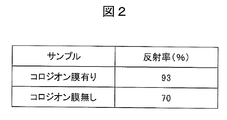
- FIG. 2 is a diagram showing a measurement result of the reflectance of the surface of the metal layer 3.
- the light reflectance of the scintillator 1 (with a collodion film) of the present disclosure was 93%.
- the reflectance was 70%. That is, when the collodion film was formed on the fluorescent layer 2, the reflectance of the aluminum film was improved.
- the measured value of the reflectance is the reflectance of light having a wavelength of 550 nm.
- FIG. 3 is an optical microscope photograph of the surface of the aluminum film according to the scintillator 1 of the present disclosure. As shown in FIG. 3, the photographed image shows the luster of the aluminum film, and it can be seen that specular reflection occurs on the aluminum film surface.
- FIG. 4 is a diagram showing a histogram of luminance in an optical microscope photograph of the surface of the aluminum film.
- the horizontal axis is the luminance
- the vertical axis is the count number. From FIG. 4, the luminance distribution of the scattered light with the luminance value 180 substantially at the center can be confirmed.
- the ratio where the luminance value was 220 or more was 12% of the total count number. That is, due to the interposition of the resin layer, specular reflection occurs in a region of about 10% or more of the surface of the aluminum film in the area of the laminate in which the aluminum layer is laminated on the phosphor layer.
- the surface roughness (Ra) of the aluminum film surface was 1.90 ⁇ m when the surface roughness (Ra) of the phosphor layer surface was vapor-deposited on the phosphor layer having a surface roughness of 2.15 ⁇ m. That is, the surface roughness (Ra) of the aluminum film surface became smaller than the surface roughness (Ra) of the phosphor layer surface.
- the flatness of the surface of the fluorescent layer 2 is excellent.
- the flatness is further improved by forming the resin layer 6 (collodion film) on the flat fluorescent layer 2.
- the metal layer 3 aluminum film
- the metal layer 3 which specularly reflected in a region of 10% or more of the whole could be formed.
- the resin layer 6 between the fluorescent layer 2 and the metal layer 3 even if the metal layer 3 has high flatness, the adhesiveness of the metal layer 3 is improved, and the metal layer 3 is peeled off. It became difficult.
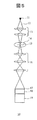
- FIG. 5 is a schematic diagram of a general transmission electron microscope 50 equipped with the CCD camera 19.
- the optical system of the transmission electron microscope 50 includes an electron gun 11, a condenser lens 13, an objective lens 14, and an imaging lens 16.
- the electron beam 12 emitted from the electron gun 11 is irradiated on a sample 15 arranged in a magnetic field of an objective lens 14 after the spot size of the electron beam 12 is adjusted by a condenser lens 13.
- the electron beam 12 is transmitted through the sample 15 to form an image, and is then enlarged by the objective lens 14 and the imaging lens 16 to form a transmission electron microscope image on the scintillator 17.
- the transmission electron microscope image is converted into an optical image by a scintillator 17 and projected on a light receiving surface of a CCD camera 19 by an optical fiber plate or an optical lens 18.
- FIG. 6 is a diagram illustrating an observation system 7 of a transmission electron microscope to which the scintillator 1 of the present disclosure is applied.
- the observation system 7 includes a column 8, a fluorescent screen 9, a multiport 10, and a CCD camera 19.
- the disclosed scintillator 1 is mounted at a position indicated by a lead wire 17.
- FIG. 7 is a diagram showing the relationship between the acceleration voltage of the electron beam and the emission intensity of the scintillator 1.
- FIG. 7 shows the case where the average thickness of the fluorescent layer 2 of the scintillator 1 is 18 ⁇ m and the case where it is 7 ⁇ m.
- the scintillator 1 in the application example 1 was formed by dropping 20 ⁇ l of a collodion solution having a concentration of 2% by mass / volume percent with the amount of the 10% aqueous solution of water glass when forming the fluorescent layer 2 being 60 ml.
- the thickness of the aluminum film was 100 nm.
- the emission intensity was high when the electron beam acceleration voltage was 80 kV.
- the average thickness of the fluorescent layer 2 was 7 ⁇ m, the emission intensity was high when the electron beam acceleration voltage was 40 kV.
- the average film thickness of the fluorescent layer 2 is small, the scattering of the electron beam and the light scattering width are narrow, and the resolution is improved. In other words, if the average film thickness of the fluorescent layer 2 is reduced, an electron beam image can be converted into a good optical image even with an electron beam at a low accelerating voltage, and a good image can be obtained with a transmission electron microscope. .
- the scintillator 1 having an average film thickness of 9 ⁇ m of the fluorescent layer 2 was used, a high luminous intensity was shown with respect to an electron beam having a low acceleration voltage of 40 kV.
- the scintillator 1 of application example 2 is the same as the method of forming the fluorescent layer 2 provided in the scintillator 1 of application example 1, except that the amount of the 10% aqueous water glass solution to be added is 30 ml, the amount of the collodion solution is 10 ⁇ l, and the average film of the aluminum film is The thickness was made 200 nm. The average thickness of the fluorescent layer 2 provided in the scintillator 1 is 18 ⁇ m.
- the scintillator 2 of the application example 2 is a scintillator in which the amount of the collodion solution dropped is 10 ⁇ l to improve the adhesion of the aluminum film.
- the scintillator 1 of the application example 2 when the electron beam of the acceleration voltage of 40 kV was irradiated, a high emission intensity was obtained. Therefore, the scintillator 1 of the present disclosure was able to convert an electron beam image into a good light image even with a low acceleration voltage electron beam, and a good image could be obtained with a transmission electron microscope. The same performance was exhibited even when the average thickness of the fluorescent layer 2 was 9 ⁇ m.
- FIG. 8 is a diagram showing an electron beam detector of a transmission electron microscope equipped with an electron beam energy loss spectroscopy (EELS) device.
- the transmission electron microscope has a detection unit (including a scintillator 32, a mirror 33, and a CCD camera 34) for observation of a transmission electron beam image and a detection unit (magnetic field prism 35, scintillator 36 and a CCD camera 37).
- the CCD camera for observing the transmitted electron beam image is structured to move in the front-back direction.
- the CCD camera is moved so that the scintillator 32 is arranged at the position of the optical axis of the electron beam.
- the transmitted electron image converted into an optical image by the scintillator 32 is transferred to a photosensitive surface of a CCD camera 34 via a mirror 33.
- the detection unit for observing the transmitted electron image is returned to the rear position, and the transmitted electron beam is made incident on the magnetic field prism 35. Then, an electron beam intensity distribution reflecting the energy spectrum of the transmitted electron beam is projected onto the EELS scintillator 36, or a two-dimensional energy filter image obtained by forming an energy-separated transmitted electron beam into an EELS scintillator is formed. 36.
- the electron beam intensity distribution and the energy filter image are converted into a light intensity distribution by the scintillator 36 and measured by the EELS measurement CCD camera 37.
- the scintillator 1 of the present disclosure can be applied to both the scintillator 32 and the EELS scintillator 36 described above.
- the scintillator 1 of the present disclosure has a phosphor layer 2 formed by a plurality of phosphor particles, a resin layer 6 (collodion film) laminated adjacent to the phosphor layer 2, and a resin layer 6 laminated adjacent to the resin layer 6.
- a metal layer 3 (aluminum film).
- the thickness of the phosphor layer 2 can be reduced by setting the average particle diameter of the phosphor for forming the phosphor layer 2 to 2 ⁇ m or less, for example. Therefore, the scintillator 1 of the present disclosure has a high optical image resolution because the average thickness of the fluorescent layer 2 is small.
- the scintillator 1 of the present disclosure includes the metal layer 3 having excellent flatness by forming the metal layer 3 on the resin layer 6. Therefore, light is specularly reflected in a region of 10% or more of the metal layer 3, and a sufficiently bright light image can be captured even when the thickness of the fluorescent layer 2 is small.
- the fluorescent layer 2 included in the scintillator 1 of the present disclosure may have an average thickness of 10 ⁇ m or less.
- the scintillator 1 of the present disclosure can capture a sufficiently bright and high-resolution optical image even when the thickness of the fluorescent layer 2 is 10 ⁇ m or less.
- the scintillator 1 of the present disclosure can be applied to a scanning electron microscope, an EELS device, and the like, in addition to a transmission electron microscope.
Landscapes
- Chemical & Material Sciences (AREA)
- Analytical Chemistry (AREA)
- Measurement Of Radiation (AREA)
Abstract
荷電粒子線検出器であって、蛍光体粒子よりなる蛍光層と、金属層とが積層された積層体を備える荷電粒子線検出器において、前記金属層および前記蛍光層の間に設けられた樹脂層を備えることを特徴とする。
Description
本開示は、荷電粒子を検出するシンチレータを備えた荷電粒子線検出器およびそれを用いた荷電粒子線装置に関する。
透過電子顕微鏡像を撮像する場合、試料を透過した電子線の透過像を対物レンズと結像レンズとで拡大してシンチレータ上に投影する。そして、シンチレータによって透過電子線の像を光像に変換し、高精細CCD(Charge Coupled Device)カメラを用いて光像を撮影する。高精細な高倍率像を十分な明るさで撮像するためには、シンチレータによって生成した光像を滲みなく高効率でCCDカメラの受光面に投影することが必要である。
また、透過型電子顕微鏡や走査電子顕微鏡など、電子線エネルギー損失分光装置(以下、EELS装置)を搭載した電子顕微鏡においては、試料を透過した後、分光器でエネルギー分光したスペクトル像またはエネルギーフィルタ像をEELS装置が備えるシンチレータ上に投影する。そしてシンチレータによって、スペクトル像またはエネルギーフィルタ像を光像に変換し、高精細CCDカメラが当該光像を撮影する。
EELS装置においても、低加速電圧の電子線によって得られるスペクトル像またはエネルギーフィルタ像を高精細な高倍率像として十分な明るさで撮像するためには、シンチレータにおいて変換された光像を滲みなく高効率でCCDカメラの受光面に投影することが必要である。
特許文献1には、近接場光学観察装置が備える入射窓(電子線励起により発光可能な発光材料を有している発光層を有している)において、膜厚を薄くしても、強度を保つためにコロジオンを用いる手法が開示されている。また、特許文献2には、画像表示装置の製造工程であって、蛍光膜とアルミニウム膜の間にコロジオン膜を設け、その後焼成して上記コロジオン膜を焼き飛ばす工程が開示されている。
近年、CCDカメラの画素の高精細化に伴い、透過電子線像を高解像且つ高効率で光像に変換することができるシンチレータが求められている。また、電子顕微鏡は、観察する試料に応じて幅広い加速電圧範囲で使用できることが必要とされている。特に生体試料や軽元素材料などの透過電子顕微鏡像を高コントラストで撮像するために、低加速電圧でも発光強度が高いシンチレータが求められている。
また、透過型電子顕微鏡または走査電子顕微鏡にEELS装置を搭載した電子顕微鏡においても、エネルギー分光したスペクトル像またはエネルギーフィルタ像を撮影するシンチレータが低加速電圧に対応する必要がある。そのためには、低加速電圧の場合であってもシンチレータの発光強度が大きくなる構成が必要となる。したがって、低加速電圧から高加速電圧までの幅広い加速レンジで使用でき、且つ十分な発光強度を持つシンチレータの開発が急務である。
シンチレータによって生成する光像の解像度を高めるためには、例えば、蛍光層が射出した光を鏡面反射する平坦性の高い金属層で蛍光層を覆う必要がある。特許文献1に記載されたシンチレータ検出器は、蛍光膜を固めるために接着剤としてコロジオンを使用することが記載されているものの、蛍光膜の凹凸を均すことは開示されていない。また、特許文献2では、蛍光膜とアルミニウム膜の間にコロジオン膜を設けることが記載されているものの、その後焼成してコロジオン膜を焼き飛ばすことが記載されており、蛍光膜とアルミニウム膜の接着にコロジオンは使用されていない。
本開示は、上記課題に鑑みてなされたものであり、電子線像を高解像且つ高効率で光像に変換することができる技術を提供することにある。
本開示は、上記課題を解決するために、例えば、蛍光体粒子によって形成される蛍光層と、金属層とが積層された積層体を備え、荷電粒子を検出する荷電粒子線検出器において、前記金属層および前記蛍光層の間に設けられた樹脂層を備えることを特徴とする荷電粒子線検出器を提供する。
本開示によれば、電子線像を高解像且つ高効率で光像に変換することができる。上記以外の課題、構成および効果は、以下の実施の形態の説明により明らかにされる。
荷電粒子を検出するシンチレータを備えた荷電粒子線検出器は、電子等が蛍光体に高速で入射することにより発生する蛍光を検出する装置である。試料に荷電粒子線を照射する電子顕微鏡、EELS等の荷電粒子線装置に、荷電粒子線を検出するために搭載される。また、荷電粒子線検出器を、撮像装置として独立して構成してもよい。
本開示の荷電粒子線検出器は、樹脂層の一方の面に蛍光を発生する蛍光体粒子よりなる蛍光層、他方の面に金属層とが隣接して積層された積層体を備える。また、発生した蛍光を受光する受光素子等、蛍光を検知する検知手段を備える。
荷電粒子線検出器を搭載する荷電粒子線装置は、試料に荷電粒子線を照射して画像を表示する電子顕微鏡や、電子線の分光分析を行うEELS装置等がある。
また、荷電粒子を検出するシンチレータを備えるカメラにも本開示は適用可能である。
以下、添付図面を参照して本開示の種々の実施例について説明する。ただし、これらの実施例は本開示を実現するための一例に過ぎず、本開示の技術的範囲を限定するものではない。また、各図において共通の構成については同一の参照番号が付されている。
[シンチレータの構成]
始めに、本開示のシンチレータの全体的な構成を説明する。
図1は、透過型電子顕微鏡に用いる本開示のシンチレータ1の構成を示す図である。なお、本明細書の以下の説明では、シンチレータは荷電粒子線を入射して発光する素子を指し、蛍光体によって形成される蛍光層2以外にも金属層3(例えば、アルミニウム膜)、樹脂層6(例えば、コロジオン膜)、ITO(Indium Tin Oxide)層4およびガラス基板5を含む構造物をシンチレータ1と称する。
始めに、本開示のシンチレータの全体的な構成を説明する。
図1は、透過型電子顕微鏡に用いる本開示のシンチレータ1の構成を示す図である。なお、本明細書の以下の説明では、シンチレータは荷電粒子線を入射して発光する素子を指し、蛍光体によって形成される蛍光層2以外にも金属層3(例えば、アルミニウム膜)、樹脂層6(例えば、コロジオン膜)、ITO(Indium Tin Oxide)層4およびガラス基板5を含む構造物をシンチレータ1と称する。
図1に示されるように、シンチレータ1は、ガラス基板5、ITO層4、蛍光層2、樹脂層6および金属層3の順に各層または構造物が積層されて形成された積層体である。蛍光層2を形成する蛍光体は、周知の蛍光体を用いることができる。本開示では、例えば、GOS(Gd2O2S:Tb)蛍光体を用いて蛍光層2を形成する。また、金属層3は、蒸着により樹脂層6の上に積層されている。
ブラウン管用途で蛍光層を作成する場合は、蛍光層に隣接して設けられる樹脂膜は、通常製造工程において焼き飛ばされる。樹脂膜を焼き飛ばすと、樹脂膜と接して設けられている金属膜にピンホールが生じたり、金属膜の剥離が起きるため、金属膜において光が鏡面反射する割合が低下する。
透過型電子顕微鏡に用いるシンチレータの場合、照射される電子線の電流量がナノ~ピコアンペア程度の低電流であるため、電子線により樹脂層が焼けることがほとんどない。つまり、樹脂層をシンチレータに残しておいても、電子線により樹脂層が焼け、隣接する金属層にピンホールを生じさせることがない。そのため、本開示では、敢えてシンチレータ1が樹脂層6を含む構成とした。本開示のシンチレータ1に係る金属層3は、ピンホールがない連続的な膜として形成されている。
通常、蛍光層は、複数の蛍光体の粒子をバインディングして形成するため、表面が粗くなる。一方、本開示のシンチレータ1では、粒径が小さい蛍光体によって蛍光層2を作成するため、蛍光層2の表面の粗さを低下させている。また、樹脂層6を蛍光層2に積層することによって、金属層3を直接蛍光層2に積層した場合と異なり、より平坦な表面に金属層3を積層することができる。即ち、本開示のシンチレータ1は、従来よりも平坦性に優れた金属層3が形成されている。また、樹脂層6を介在させることによって、金属層3の接着性を向上させることができる。
また、ブラウン管に用いる蛍光層では、平均粒径が2~3μm程度の大きさの蛍光体を用いる場合が多い。一方、本開示では、一例として、平均粒径が1.6μmの蛍光体を用いている。即ち、本開示に係る蛍光層2はブラウン管に用いる蛍光層よりも表面が平坦である。ここで、平均粒径は、メディアン径でありD50を意味する。また、蛍光層2を形成する際の蛍光体の塗布方法は遠心塗布法であり、極めて平坦に蛍光層2を形成することが可能である。以下に、本開示のシンチレータ1の作成手順および特性評価の方法について説明する。
[蛍光層の遠心塗布]
まず、蛍光層2の形成方法について説明する。
始めに、ガラス基板5の洗浄を行った。ガラス基板5は、例えば、蛍光層2を塗布する側の表面にITO層4を形成する。ただし、シンチレータ1は、ITO層4を設けなくともよい。ITO層4は、光を透過させる透明な素材であり、且つ導電性がある。そのため、ITO層4を設けるとシンチレータ1を帯電させずに電気を逃がす役割を果たす。
まず、蛍光層2の形成方法について説明する。
始めに、ガラス基板5の洗浄を行った。ガラス基板5は、例えば、蛍光層2を塗布する側の表面にITO層4を形成する。ただし、シンチレータ1は、ITO層4を設けなくともよい。ITO層4は、光を透過させる透明な素材であり、且つ導電性がある。そのため、ITO層4を設けるとシンチレータ1を帯電させずに電気を逃がす役割を果たす。
蛍光層2を形成するための塗布液を以下のようにして用意した。まず、無水酢酸バリウム(超電導用)1.16gを純水134mlに溶かし、0.87%酢酸バリウム水溶液(1.16g/134ml)を電解水として調製した。次に、純水250mlに界面活性剤二滴を加えて撹拌した。ビーカに純水240mlを入れ、調製した0.87%酢酸バリウム水溶液60mlと界面活性剤水溶液10mlとを加えて撹拌した。次に、ビーカに蛍光体試料(GOS(Gd2O2S:Tb)蛍光体)を640mg入れて、純水を30ml加えた。粒度分布測定装置で計測した蛍光体の平均粒径(メディアン径)は、体積%の50%の値(D50)で1.6μmだった。
次に、水ガラス原液(ケイ酸カリウム)20mlに純水40mlを加えて10%水ガラス水溶液60ml(6g/(20ml+40ml))を調製した。続いて、蛍光体懸濁液を超音波洗浄機にて分散処理した。その後、蛍光体懸濁液に10%水ガラス水溶液を60ml加えて撹拌し、電解水中に注ぎ込んだ。以上のようにして塗布液を調整し、塗布液の液量は400ml(240ml+60ml+10ml+30ml+60ml)となった。
なお、上記の界面活性剤は、直鎖アルキルベンゼン系またはアルコールエーテル系の界面活性剤である。直鎖アルキルベンゼン系またはアルコールエーテル系の界面活性剤は、安価で取扱いが容易である。その他、縮合ナフタレンスルホン酸系の界面活性剤を使用した場合も、良好に蛍光層2を形成できた。
また、シリカの凝集体を防ぎたい場合には、添加する水ガラスの量を減らしてもよい。以下に、添加する水ガラスの量を半分にした場合の塗布液の調製方法を説明する。まず、ビーカに純水300mlを入れ、調製した0.87%酢酸バリウム水溶液30mlと界面活性剤水溶液10mlとを加えて撹拌した。次に、ビーカに蛍光体試料(GOS(Gd2O2S:Tb)蛍光体)を640mg入れて、純水を30ml加えた。蛍光体は上で説明したものと同じであり、平均粒径がD50で1.6μmである。
次に、水ガラス原液(ケイ酸カリウム)10mlに純水20mlを加えて10%水ガラス水溶液を30ml(3g/(10ml+20ml))調製した。続いて、蛍光体懸濁液を超音波洗浄機にて分散処理した。その後、蛍光体懸濁液に10%水ガラス水溶液を30ml加えて撹拌し、電解水中に注ぎ込んだ。以上のようにして塗布液を調整し、塗布液の液量は400ml(300ml+30ml+10ml+30ml+60ml)となった。
次に、底にガラス基板5(ITO層4はガラス基板5上にあってもなくてもよい)が設置された容器に塗布液を入れ、遠心分離機を用いて、回転数2000rpm、回転時間5minで遠心塗布を行った。
遠心塗布を実施する場合、回転角速度を上げることによって粒子に加わる遠心力が増加する。したがって、回転数を上げることにより、微細な蛍光体の粒子を短時間で基板上に塗布することができる。遠心分離機を用いずに塗布液を静置して自然沈降させて蛍光層2を形成する場合、平均粒径が1.6μm程度の微細な粒子を沈降させるには2時間程度かかる。一方、遠心塗布によって蛍光層2を形成する場合、回転数を2000rpmに設定すると、5分間程度でガラス基板5上に蛍光体2を塗布することができる。また、遠心塗布によって蛍光層2を形成した場合、蛍光体に遠心力が働くため、ガラス基板5に蛍光体が押し付けられて、密度の高い蛍光層2が得られる。
次に、遠心分離機において回転処理が済んだ容器から溶液をピペットで取り除き、容器の底からガラス基板5を取り出した。取り出したガラス基板5を自然乾燥させて蛍光層2を形成した。
[コロジオン膜の塗布]
本開示のシンチレータ1は、蛍光層2上に樹脂層6(コロジオン膜)を形成し、平坦性の高い表面を形成した後に、金属層3(アルミニウム膜)が設けられて作成される。コロジオン膜は、コロジオン膜張器を用いて蛍光層2上に形成した。コロジオン膜張器は、水面に滴下したコロジオン溶液が水面上に広がった後、溶媒の揮発または水位の低下を利用して、水面上に形成されたコロジオン膜を目的物に張り付ける湿式法の薄膜作成器である。
本開示のシンチレータ1は、蛍光層2上に樹脂層6(コロジオン膜)を形成し、平坦性の高い表面を形成した後に、金属層3(アルミニウム膜)が設けられて作成される。コロジオン膜は、コロジオン膜張器を用いて蛍光層2上に形成した。コロジオン膜張器は、水面に滴下したコロジオン溶液が水面上に広がった後、溶媒の揮発または水位の低下を利用して、水面上に形成されたコロジオン膜を目的物に張り付ける湿式法の薄膜作成器である。
コロジオン膜を形成する際に必要な用具と試薬は、以下のとおりである。
1)清浄済みのコロジオン膜張器
2)2%(質量/体積パーセント濃度)コロジオン・酢酸イソアミル溶液
3)マイクロピペット(最小分注量10μl)
4)25℃~35℃の純水500ml
1)清浄済みのコロジオン膜張器
2)2%(質量/体積パーセント濃度)コロジオン・酢酸イソアミル溶液
3)マイクロピペット(最小分注量10μl)
4)25℃~35℃の純水500ml
なお、コロジオン膜張器に入れる純水の液温が室温より低い場合、溶媒揮発時の湿度によってはコロジオン膜に穴を生じさせることがある。そのため、コロジオン膜張器に入れる純水の液温は25℃~35℃にした。
以下に、コロジオン膜の作成工程について説明する。まず、25℃~35℃の純水を400ml~500mlの入れたコロジオン膜張器の中央にメッシュ台を置き、蛍光層2の表面をプラズマ処理した積層体(ガラス基板5および蛍光層2)を上記メッシュ台上にゆっくりと沈めた。
続いて、コロジオン溶液を水面上15mmの高さから滴下し、すばやく蓋をして5分間静置した。コロジオン膜の厚さはコロジオン溶液の濃度、滴下するコロジオン溶液の液量、シャーレの大きさ、および水温で決まる。濃度が高く、滴下量が多く、シャーレが小さく、水温が高いとコロジオン膜は膜厚が厚くなる。
本開示では、コロジオン溶液の濃度が2%質量/体積パーセントであり、滴下した液量が10μlまたは20μl、シャーレの大きさが155mmφ、水温が25℃~30℃の条件でコロジオン膜の作成を実施した。
続いて、コロジオン膜張器の排水コックを開き1秒間に二滴程度の速さで排水した。コロジオン膜が張られた蛍光層2をメッシュ台に載置したまま、ゴミが付着しないようにして自然乾燥した。
上記のように、コロジオン膜は蛍光層2の上に形成される。シンチレータ1は、コロジオン膜を形成後、さらにアルミニウム膜をコロジオン膜上に蒸着することによって作成する。上述したとおり、本開示のシンチレータ1においては、コロジオン膜は焼成して焼き飛ばされることはなく、アルミニウム膜と蛍光層2との間に配置されたまま残る。
アルミニウム膜を蒸着して作成したシンチレータを、焼成温度300~400℃で焼成してコロジオン膜を焼き飛ばすと、アルミニウム膜は自然放置でも簡単に剥がれた。つまり樹脂であるコロジオン膜とアルミニウム膜とが隣接して接着した方が、アルミニウム膜を蛍光層の上に直接形成した場合よりもアルミニウム膜の接着性が向上する。
[蛍光層の厚さおよび平坦性]
蛍光層2の厚さ(蛍光層2の平均膜厚)は、例えば、以下のようにして計測することができる。本開示では蛍光層2の平均厚さをレーザフォーカス変位計を用いて計測した。蛍光層2を一部削り取りガラス基板5を剥き出しにし、ガラス基板5の位置を高さのゼロ点とする。そして、1000μmの幅に亘って1μm間隔で厚さを計測することを、測定ラインをずらして三回行い、各計測点における計測値の平均を蛍光層2の平均膜厚とする。測定ラインの間隔は、例えば、略5μmとする。
蛍光層2の厚さ(蛍光層2の平均膜厚)は、例えば、以下のようにして計測することができる。本開示では蛍光層2の平均厚さをレーザフォーカス変位計を用いて計測した。蛍光層2を一部削り取りガラス基板5を剥き出しにし、ガラス基板5の位置を高さのゼロ点とする。そして、1000μmの幅に亘って1μm間隔で厚さを計測することを、測定ラインをずらして三回行い、各計測点における計測値の平均を蛍光層2の平均膜厚とする。測定ラインの間隔は、例えば、略5μmとする。
上記の計測方法以外にも、蛍光層2の膜重量から厚さの推測値を算出することも可能である。例えば、出荷用の製品では、蛍光層2を削って膜厚を測定することはできないため上記推測値を算出する。蛍光層2の平均膜厚(推測値)は、蛍光層2の単位面積当たりの重量から蛍光層2のトップ面(層が最も厚い部分)の膜厚を算出し、当該膜厚から蛍光層2表面の凹凸分を差し引いて求める。
以下に、膜厚の平均膜厚(推測値)の算出を行った例を示す。
まず、蛍光層2を形成する前に積層体(ガラス基板5+ITO層4)の重量を計測し、蛍光層2を形成した後に、再度積層体(ガラス基板5+ITO層4+蛍光層2)の重量を計測した。積層体の重量は、蛍光層2を形成する前と後とで、1.4887gから1.5448gに変化した。言い換えると、蛍光層2の重量は、
1.5448(g) - 1.4887(g) = 56.1(mg)
である。また、ガラス基板5の面積は9.61cm2であったため、面積当たりの平均膜重量は、
56.1mg ÷ 9.61cm2 = 5.84mg/cm2
となる。
まず、蛍光層2を形成する前に積層体(ガラス基板5+ITO層4)の重量を計測し、蛍光層2を形成した後に、再度積層体(ガラス基板5+ITO層4+蛍光層2)の重量を計測した。積層体の重量は、蛍光層2を形成する前と後とで、1.4887gから1.5448gに変化した。言い換えると、蛍光層2の重量は、
1.5448(g) - 1.4887(g) = 56.1(mg)
である。また、ガラス基板5の面積は9.61cm2であったため、面積当たりの平均膜重量は、
56.1mg ÷ 9.61cm2 = 5.84mg/cm2
となる。
上記面積当たりの膜重量を、予め特定しておいた膜厚1μmおよび面積1cm2あたりの膜重量で除することによって蛍光層2の厚さを決定することができる。膜厚1μmおよび面積1cm2あたりの膜重量は、例えば、SEM観察によって膜厚を計測し、蛍光層2の重量を当該膜厚とガラス基板5の面積で除することによって予め決定しておく。ここでSEM観察によって計測する膜厚は、例えば、蛍光層2のトップ面(層が最も厚い部分)に対応する膜厚である。遠心塗布を行って製膜したサンプルでは、膜厚1μmおよび面積1cm2あたりの膜重量は、0.249mg/cm2であった。
したがって、蛍光層2の膜厚は、
5.84mg/cm2 ÷ 0.249(mg/cm2)/μm = 23.4μm
となる。ここで、予め特定しておいた膜厚1μmおよび面積1cm2あたりの膜重量は、蛍光層2のトップ面の膜厚に基づいて決定された値であるため、この膜厚も蛍光層2のトップ面に対応する膜厚となる。
5.84mg/cm2 ÷ 0.249(mg/cm2)/μm = 23.4μm
となる。ここで、予め特定しておいた膜厚1μmおよび面積1cm2あたりの膜重量は、蛍光層2のトップ面の膜厚に基づいて決定された値であるため、この膜厚も蛍光層2のトップ面に対応する膜厚となる。
蛍光層2の平均膜厚は、蛍光層2のトップ面に対応する膜厚から蛍光層2の凹凸分を差し引いた値である。レーザフォーカス変位計で計測した平均膜厚とSEMで決定したトップ面に対応する膜厚との差は、およそ5μm(上記凹凸の深さの半分の値)であった。したがって、蛍光層2の平均膜厚は、
23.4μm - 5.0μm = 18.4μm
となる。以上のようにして、蛍光層2の平均膜厚(推測値)が求められる。
23.4μm - 5.0μm = 18.4μm
となる。以上のようにして、蛍光層2の平均膜厚(推測値)が求められる。
なお、実際に複数の蛍光層の平均膜厚を計測した結果、平均膜厚が0~20μmの範囲内である場合、蛍光層の厚みの最大部分と最少部分の凹凸(Rz)の半分の長さは、どの蛍光層もおよそ5.0μm(上記凹凸の深さの半分の値)程度であった。後述する蛍光層の表面粗さ(Ra)は、およそ2.0μm程度であり、表面粗さ(Ra)の4~5倍程度の値が蛍光層の凹凸の深さとなっている。以下に、蛍光層2の表面粗さ(Ra)の計測方法について説明する。
蛍光層2の表面粗さ(Ra)は、蛍光層2の厚さの計測と同様、レーザフォーカス変位計を用いて計測した。レーザの当たる場所に蛍光層2を塗布したガラス基板5を設置し、蛍光層2の表面にフォーカスを合わせて計測を行った。1000μmの幅に亘って1μm間隔で厚さを計測することを、測定ラインをずらして三回行い、表面粗さ(Ra)の平均を求めた。表面粗さ(Ra)は式1で求められる。

ここで、L:測定幅(μm)、f(x):粗さ曲線(μm)である。粗さ曲線は、レーザフォーカス変位計で計測した各計測位置での値の積算値を測定回数で除して平均値を求め、計測位置xと、計測位置xにおける測定値から平均値を差し引いた値f(x)(平均差)とを対応づけた関数である。表面粗さ(Ra)は、平均差f(x)の絶対値を積算して測定幅Lで除した値である。
今回作成した蛍光層2の平坦性Raは、測定を三回実施した結果、2.165μm、2.397μmおよび2.323μmと測定された。これは、上で説明したラインを三回ずらす測定を三回実施した結果である。三回の測定結果の平均した表面粗さ(Ra)は2.295μmとなった。
蛍光層2の表面粗さ(Ra)を計測した後に、蛍光層2上に樹脂層6(コロジオン膜)を形成した。同様の方法により樹脂層6の表面粗さ(Ra)を三回計測したところ、2.044μm、1.939μmおよび2.028μmとなった。三回の測定結果を平均した表面粗さ(Ra)は2.004μmとなった。つまり、コロジオン膜を形成することによって、表面粗さ(Ra)が0.291μm低下した。即ち、樹脂層6の表面粗さは蛍光層2の表面粗さよりも小さく、シンチレータ1の平坦性が向上した。
蛍光層2および樹脂層6の表面粗さ(Ra)の別の計測結果は以下のとおりであった。その結果、蛍光層の表面粗さ(Ra)は、2.211μm、2.195μmおよび2.212μmであり、三回の測定結果を平均した表面粗さ(Ra)は2.206μmとなった。一方、樹脂層6(コロジオン膜)形成後の表面粗さ(Ra)は、2.183μm、2.157μmおよび2.133μmであり、三回の測定結果を平均した表面粗さ(Ra)は2.158μmとなった。即ち、コロジオン膜を形成することにより表面粗さ(Ra)は0.048μm低下し、シンチレータ1の平坦性が向上した。
上記のとおり、コロジオン膜を蛍光層2の上に形成することによって、二回の測定ともシンチレータ1の平坦性の向上を確認できた。なお、例えば、蛍光体の平均粒径(D50)を2μm以下とすることによって蛍光層2の厚みを薄くし、且つ平坦性を向上することができる。
平坦性に優れる樹脂層6(コロジオン膜)の上にアルミニウム膜を蒸着することにより、金属層3(アルミニウム膜)の平坦性は向上した(または表面粗さ(Ra)が低下した)。平坦性の高い金属層3を形成することによって、反射率が向上し明るい光像を撮影できるようになる。以下に、アルミニウム膜の反射率について説明する。
[アルミニウム膜の反射率]
続いて、作成したシンチレータ1の金属層3の表面の反射率を測定した。
図2は、金属層3の表面の反射率の測定結果を示す図である。本開示のシンチレータ1(コロジオン膜あり)の光の反射率は93%であった。一方、コロジオン膜を設けずに蛍光層2の上に直接アルミニウム膜を蒸着させたシンチレータでは、反射率は70%だった。即ち、蛍光層2の上にコロジオン膜を形成すると、アルミニウム膜の反射率が向上した。なお、上記の測定で反射率の測定値は波長が550nmの光の反射率である。
続いて、作成したシンチレータ1の金属層3の表面の反射率を測定した。
図2は、金属層3の表面の反射率の測定結果を示す図である。本開示のシンチレータ1(コロジオン膜あり)の光の反射率は93%であった。一方、コロジオン膜を設けずに蛍光層2の上に直接アルミニウム膜を蒸着させたシンチレータでは、反射率は70%だった。即ち、蛍光層2の上にコロジオン膜を形成すると、アルミニウム膜の反射率が向上した。なお、上記の測定で反射率の測定値は波長が550nmの光の反射率である。
図3は、本開示のシンチレータ1に係るアルミニウム膜の表面の光学顕微鏡写真である。図3に示されているとおり、撮像した写真にはアルミニウム膜の光沢が現れており、アルミニウム膜表面において鏡面反射が起きていることがわかる。
図4は、アルミニウム膜表面の光学顕微鏡写真における輝度のヒストグラムを示す図である。図4において、横軸が輝度であり、縦軸がカウント数である。図4からは、輝度値180を概ね中心にした散乱光の輝度分布が確認できる。また、輝度220以上の位置に鏡面反射と考えられる強い光の分布が存在する。輝度値が220以上の割合は、全体のカウント数の12%だった。すなわち、樹脂層が介在することにより、蛍光体層にアルミニウム層が積層されている積層体面積のうち、アルミニウム膜表面のおよそ10%以上の領域において鏡面反射している。
また、アルミニウム膜表面の表面粗さ(Ra)は、蛍光層表面の表面粗さ(Ra)が2.15μmの蛍光層上に蒸着した場合に1.90μmだった。すなわち、アルミニウム膜表面の表面粗さ(Ra)は、蛍光層表面の表面粗さ(Ra)よりも小さくなった。
本開示では、平均粒径が小さい蛍光体(平均粒径1.6μm)を用いて蛍光層2を作成したため、蛍光層2の表面の平坦性が優れている。その上、本開示のシンチレータ1では、平坦な蛍光層2の上に樹脂層6(コロジオン膜)を形成することによってさらに平坦性を向上させた。そして、当該樹脂層6の上に金属層3(アルミニウム膜)を蒸着することにより、平坦性の高い金属層3を形成した。その結果、全体の10%以上の領域で鏡面反射する金属層3を作成できた。また、蛍光層2と金属層3の間に樹脂層6を形成することにより、平坦性の高い金属層3であっても、金属層3の接着性が向上し、金属層3の剥がれが起きにくくなった。
以下に、本開示のシンチレータ1を種々の装置に適用した適用例1~3について説明する。
(適用例1)
まず、図5を参照して一般的な透過電子顕微鏡50について概略的に説明する。
図5は、CCDカメラ19を搭載した一般的な透過電子顕微鏡50の概略図である。透過電子顕微鏡50の光学系は、電子銃11、コンデンサレンズ13、対物レンズ14および結像レンズ16から構成される。
(適用例1)
まず、図5を参照して一般的な透過電子顕微鏡50について概略的に説明する。
図5は、CCDカメラ19を搭載した一般的な透過電子顕微鏡50の概略図である。透過電子顕微鏡50の光学系は、電子銃11、コンデンサレンズ13、対物レンズ14および結像レンズ16から構成される。
電子銃11から放出された電子線12は、コンデンサレンズ13で電子線12のスポットサイズが調整された後、対物レンズ14の磁場内に配置された試料15に照射される。電子線12は、試料15を透過して像が形成された後、対物レンズ14および結像レンズ16で拡大され、シンチレータ17に透過電子顕微鏡像を結像する。透過電子顕微鏡像は、シンチレータ17によって光像に変換され、光ファイバプレートまたは光学レンズ18でCCDカメラ19の受光面に投影される。
続いて、透過型電子顕微鏡の観察システムに本開示のシンチレータ1を搭載した例について図6を参照しながら説明する。
図6は、本開示のシンチレータ1を適用した透過型電子顕微鏡の観察システム7を示す図である。観察システム7は、カラム8、蛍光板9、マルチポート10、およびCCDカメラ19から構成されている。本開示ノシンチレータ1は、引き出し線17で示された位置に搭載されている。
図6は、本開示のシンチレータ1を適用した透過型電子顕微鏡の観察システム7を示す図である。観察システム7は、カラム8、蛍光板9、マルチポート10、およびCCDカメラ19から構成されている。本開示ノシンチレータ1は、引き出し線17で示された位置に搭載されている。
図7は、電子線の加速電圧とシンチレータ1における発光強度との関係を示す図である。図7には、シンチレータ1の蛍光層2の平均膜厚が18μmのものと7μmのものとが示されている。なお、適用例1におけるシンチレータ1は、蛍光層2を形成する際の10%水ガラス水溶液の量を60mlとし、コロジオン溶液は濃度が2%質量/体積パーセントのものを20μl滴下して形成した。また、アルミニウム膜の膜厚は100nmとした。
図7に示されているように、蛍光層2の平均膜厚が18μmの場合は、電子線の加速電圧が80kVのときに高い発光強度となった。また、蛍光層2の平均膜厚が7μmの場合は、電子線の加速電圧40kVのときに高い発光強度となった。また、蛍光層2の平均膜厚が薄いため、電子線の散乱および光散乱幅が狭く、解像度が向上した。つまり、蛍光層2の平均膜厚を小さくすれば低加速電圧の電子線でも、電子線の像を良好な光像に変換することができ、良好な画像を透過型電子顕微鏡で得ることができる。なお、蛍光層2の平均膜厚が9μmのシンチレータ1を使用した場合も同様に、低加速電圧40kVの電子線に対して高い発光強度を示した。
(適用例2)
適用例2のシンチレータ1は、適用例1のシンチレータ1が備える蛍光層2の形成方法において、添加する10%水ガラス水溶液の量を30mlとし、コロジオン溶液の量を10μlとし、アルミニウム膜の平均膜厚を200nmとして作成した。また、蛍当該シンチレータ1が備える蛍光層2の平均膜厚は18μmである。適用例2のシンチレータ2は滴下するコロジオン溶液の量を10μlとすることで、アルミニウム膜の密着性を向上させたシンチレータである。
適用例2のシンチレータ1は、適用例1のシンチレータ1が備える蛍光層2の形成方法において、添加する10%水ガラス水溶液の量を30mlとし、コロジオン溶液の量を10μlとし、アルミニウム膜の平均膜厚を200nmとして作成した。また、蛍当該シンチレータ1が備える蛍光層2の平均膜厚は18μmである。適用例2のシンチレータ2は滴下するコロジオン溶液の量を10μlとすることで、アルミニウム膜の密着性を向上させたシンチレータである。
適用例2のシンチレータ1では、加速電圧40kVの電子線を照射した場合に、高い発光強度が得られた。したがって、低加速電圧の電子線でも、本開示のシンチレータ1は電子線の像を良好な光像に変換することができ、良好な画像を透過型電子顕微鏡で得ることができた。なお、蛍光層2の平均膜厚が9μmのものであっても同様の性能を示した。
(適用例3)
続いて、電子線エネルギー損失分光(EELS)装置が搭載された透過電子顕微鏡にも本開示のシンチレータ1を適用できることを説明する。
続いて、電子線エネルギー損失分光(EELS)装置が搭載された透過電子顕微鏡にも本開示のシンチレータ1を適用できることを説明する。
図8は、電子線エネルギー損失分光(EELS)装置が搭載された透過電子顕微鏡の電子線検出部を示す図である。図8に示されているとおり、透過電子顕微鏡は、透過電子線像観察用の検出部(シンチレータ32、ミラー33およびCCDカメラ34を含む)とエネルギースペクトル観察用の検出部(磁場プリズム35、シンチレータ36およびCCDカメラ37を含む)との二つの検出部を備える。
透過電子線像観察用のCCDカメラ34は前後方向に移動する構造となっており、透過電子像観察時にはシンチレータ32が電子線38の光軸の位置に配置されるようにCCDカメラ34を移動する。シンチレータ32で光像に変換された透過電子像はミラー33を介してCCDカメラ34の感光面に転写される。
一方、電子線エネルギー損失分光測定時は、透過電子像観察用の検出部を後ろの位置に戻して、透過電子線を磁場プリズム35に入射させる。そして、透過電子線のエネルギースペクトルを反映した電子線強度分布が、EELS用シンチレータ36上に投射されるか、または、エネルギー分光した透過電子線を結像した2次元エネルギーフィルタ像が、EELS用シンチレータ36上に投影される。この電子線強度分布やエネルギーフィルタ像をシンチレータ36で光強度分布に変換し、EELS測定用CCDカメラ37で測定する。
上で説明したシンチレータ32およびEELS用シンチレータ36の双方に本開示のシンチレータ1を適用することができる。
[まとめ]
本開示のシンチレータ1は、複数の蛍光体粒子によって形成される蛍光層2と、蛍光層2に隣接して積層された樹脂層6(コロジオン膜)と、樹脂層6と隣接して積層された金属層3(アルミニウム膜)と、を備える。例えば、蛍光層2を形成するための蛍光体の平均粒径を、例えば、2μm以下とすることによって蛍光層2の厚みを薄くすることができる。したがって、本開示のシンチレータ1は、蛍光層2の平均膜厚が薄いために光像の解像度が高い。さらに、本開示のシンチレータ1は、樹脂層6の上に金属層3を形成することによって、平坦性の優れた金属層3を備える。したがって、金属層3の10%以上の領域で光が鏡面反射し、蛍光層2の膜厚が薄くても十分に明るい光像を撮影できる。一例として、本開示のシンチレータ1が備える蛍光層2は、平均厚さが10μm以下であってもよい。本開示のシンチレータ1は、蛍光層2の厚さが10μm以下であっても、十分に明るく高解像度な光像を撮影できる。また、本開示のシンチレータ1は、透過型電子顕微鏡の他、走査型電子顕微鏡およびEELS装置等に適用することができる。
本開示のシンチレータ1は、複数の蛍光体粒子によって形成される蛍光層2と、蛍光層2に隣接して積層された樹脂層6(コロジオン膜)と、樹脂層6と隣接して積層された金属層3(アルミニウム膜)と、を備える。例えば、蛍光層2を形成するための蛍光体の平均粒径を、例えば、2μm以下とすることによって蛍光層2の厚みを薄くすることができる。したがって、本開示のシンチレータ1は、蛍光層2の平均膜厚が薄いために光像の解像度が高い。さらに、本開示のシンチレータ1は、樹脂層6の上に金属層3を形成することによって、平坦性の優れた金属層3を備える。したがって、金属層3の10%以上の領域で光が鏡面反射し、蛍光層2の膜厚が薄くても十分に明るい光像を撮影できる。一例として、本開示のシンチレータ1が備える蛍光層2は、平均厚さが10μm以下であってもよい。本開示のシンチレータ1は、蛍光層2の厚さが10μm以下であっても、十分に明るく高解像度な光像を撮影できる。また、本開示のシンチレータ1は、透過型電子顕微鏡の他、走査型電子顕微鏡およびEELS装置等に適用することができる。
1…シンチレータ
2…蛍光体
3…アルミニウム膜
4…ITO膜
5…ガラス板
6…樹脂膜
7…観察システム
8…カラム
9…蛍光板
10…マルチポート
11…電子銃
12…電子線
13…コンデンサレンズ
14…対物レンズ
15…試料
16…結像レンズ
17…シンチレータ
18…光ファイバプレートまたは光学レンズ
19…CCDカメラ
31…結像レンズ
32…シンチレータ
33…ミラー
34…CCDカメラ
35…磁場プリズム
36…EELS用シンチレータ
37…EELS測定用CCD
38…電子線
2…蛍光体
3…アルミニウム膜
4…ITO膜
5…ガラス板
6…樹脂膜
7…観察システム
8…カラム
9…蛍光板
10…マルチポート
11…電子銃
12…電子線
13…コンデンサレンズ
14…対物レンズ
15…試料
16…結像レンズ
17…シンチレータ
18…光ファイバプレートまたは光学レンズ
19…CCDカメラ
31…結像レンズ
32…シンチレータ
33…ミラー
34…CCDカメラ
35…磁場プリズム
36…EELS用シンチレータ
37…EELS測定用CCD
38…電子線
Claims (11)
- 蛍光体粒子によって形成される蛍光層と、金属層とが積層された積層体を備え、荷電粒子を検出する荷電粒子線検出器において、
前記金属層および前記蛍光層の間に設けられた樹脂層を備えることを特徴とする荷電粒子線検出器。 - 請求項1において、
前記樹脂層はコロジオン膜であることを特徴とする荷電粒子線検出器。 - 請求項1において、
前記樹脂層の前記蛍光層と接する面の表面粗さ(第一のRa)は、前記樹脂層の前記金属層と接する面の表面粗さ(第2のRa)よりも大きいことを特徴とする荷電粒子線検出器。 - 請求項1において、
前記金属層が光を鏡面反射する領域の面積は、前記金属層と前記樹脂層とが接する面積の10%以上であることを特徴とする荷電粒子線検出器。 - 請求項1において、
前記金属層は、前記金属層と前記樹脂層とが接する領域内にピンホールがないことを特徴とする荷電粒子線検出器。 - 請求項1において、
前記蛍光層の平均厚さが10μm以下であることを特徴とする荷電粒子線検出器。 - 請求項1において、
前記金属層は、アルミニウム膜であることを特徴とする荷電粒子線検出器。 - 請求項1に記載において、
前記蛍光体粒子の平均粒径が2μm以下であることを特徴とする荷電粒子線検出器。 - 請求項1ないし8のいずれかに記載の荷電粒子線検出器を備える電子顕微鏡。
- 請求項1ないし8のいずれかに記載の荷電粒子線検出器を備える電子線エネルギー損失分光装置。
- 請求項1ないし8のいずれかに記載の荷電粒子線検出器を備える撮像装置。
Priority Applications (2)
| Application Number | Priority Date | Filing Date | Title |
|---|---|---|---|
| CN201880094245.1A CN112236838B (zh) | 2018-07-03 | 2018-07-03 | 带电粒子束检测器、电子显微镜、电子束能量损失分光装置以及摄像装置 |
| PCT/JP2018/025207 WO2020008526A1 (ja) | 2018-07-03 | 2018-07-03 | 荷電粒子線検出器、電子顕微鏡、電子線エネルギー損失分光装置および撮像装置 |
Applications Claiming Priority (1)
| Application Number | Priority Date | Filing Date | Title |
|---|---|---|---|
| PCT/JP2018/025207 WO2020008526A1 (ja) | 2018-07-03 | 2018-07-03 | 荷電粒子線検出器、電子顕微鏡、電子線エネルギー損失分光装置および撮像装置 |
Publications (1)
| Publication Number | Publication Date |
|---|---|
| WO2020008526A1 true WO2020008526A1 (ja) | 2020-01-09 |
Family
ID=69060941
Family Applications (1)
| Application Number | Title | Priority Date | Filing Date |
|---|---|---|---|
| PCT/JP2018/025207 Ceased WO2020008526A1 (ja) | 2018-07-03 | 2018-07-03 | 荷電粒子線検出器、電子顕微鏡、電子線エネルギー損失分光装置および撮像装置 |
Country Status (2)
| Country | Link |
|---|---|
| CN (1) | CN112236838B (ja) |
| WO (1) | WO2020008526A1 (ja) |
Cited By (1)
| Publication number | Priority date | Publication date | Assignee | Title |
|---|---|---|---|---|
| JPWO2021234800A1 (ja) * | 2020-05-18 | 2021-11-25 |
Citations (6)
| Publication number | Priority date | Publication date | Assignee | Title |
|---|---|---|---|---|
| JPH02204956A (ja) * | 1989-01-25 | 1990-08-14 | Nippon Denshi Tekunikusu Kk | 走査形電子顕微鏡 |
| JP2002131438A (ja) * | 2000-10-26 | 2002-05-09 | Canon Inc | 放射線検出装置およびこれを用いた放射線画像形成装置 |
| JP2004214057A (ja) * | 2003-01-06 | 2004-07-29 | Hitachi High-Technologies Corp | 電子線分光器、それを備えた電子顕微鏡及び分析方法 |
| JP2005009872A (ja) * | 2003-06-16 | 2005-01-13 | Canon Inc | シンチレーションプレートおよびその製造方法 |
| JP2013508905A (ja) * | 2009-10-23 | 2013-03-07 | サーモ フィッシャー サイエンティフィック (ブレーメン) ゲーエムベーハー | 荷電粒子を検出する検出装置、荷電粒子を検出する方法および質量分析計 |
| JP2015005351A (ja) * | 2013-06-19 | 2015-01-08 | 日本電子株式会社 | 検出器および荷電粒子線装置 |
Family Cites Families (3)
| Publication number | Priority date | Publication date | Assignee | Title |
|---|---|---|---|---|
| JP2008226745A (ja) * | 2007-03-15 | 2008-09-25 | Toshiba Corp | メタルバック付き蛍光面とその製造方法および画像表示装置 |
| JP2013026152A (ja) * | 2011-07-25 | 2013-02-04 | Hitachi High-Technologies Corp | 電子顕微鏡 |
| CN103805161B (zh) * | 2013-12-13 | 2016-05-25 | 北京中科科仪股份有限公司 | 一种二次电子探测器闪烁体的制备方法 |
-
2018
- 2018-07-03 WO PCT/JP2018/025207 patent/WO2020008526A1/ja not_active Ceased
- 2018-07-03 CN CN201880094245.1A patent/CN112236838B/zh active Active
Patent Citations (6)
| Publication number | Priority date | Publication date | Assignee | Title |
|---|---|---|---|---|
| JPH02204956A (ja) * | 1989-01-25 | 1990-08-14 | Nippon Denshi Tekunikusu Kk | 走査形電子顕微鏡 |
| JP2002131438A (ja) * | 2000-10-26 | 2002-05-09 | Canon Inc | 放射線検出装置およびこれを用いた放射線画像形成装置 |
| JP2004214057A (ja) * | 2003-01-06 | 2004-07-29 | Hitachi High-Technologies Corp | 電子線分光器、それを備えた電子顕微鏡及び分析方法 |
| JP2005009872A (ja) * | 2003-06-16 | 2005-01-13 | Canon Inc | シンチレーションプレートおよびその製造方法 |
| JP2013508905A (ja) * | 2009-10-23 | 2013-03-07 | サーモ フィッシャー サイエンティフィック (ブレーメン) ゲーエムベーハー | 荷電粒子を検出する検出装置、荷電粒子を検出する方法および質量分析計 |
| JP2015005351A (ja) * | 2013-06-19 | 2015-01-08 | 日本電子株式会社 | 検出器および荷電粒子線装置 |
Cited By (3)
| Publication number | Priority date | Publication date | Assignee | Title |
|---|---|---|---|---|
| JPWO2021234800A1 (ja) * | 2020-05-18 | 2021-11-25 | ||
| WO2021234800A1 (ja) * | 2020-05-18 | 2021-11-25 | 株式会社日立ハイテク | 透過電子顕微鏡 |
| JP7332803B2 (ja) | 2020-05-18 | 2023-08-23 | 株式会社日立ハイテク | 透過電子顕微鏡 |
Also Published As
| Publication number | Publication date |
|---|---|
| CN112236838B (zh) | 2024-04-26 |
| CN112236838A (zh) | 2021-01-15 |
Similar Documents
| Publication | Publication Date | Title |
|---|---|---|
| US7242470B2 (en) | Multilayered surface-enhanced Raman scattering substrates | |
| US5552602A (en) | Electron microscope | |
| US20180080885A1 (en) | Cathodoluminescence-activated nanoscale imaging | |
| CN1656373A (zh) | 元素特定的x射线荧光显微镜以及操作方法 | |
| JP2001512568A (ja) | 軟x線顕微透視装置 | |
| US5932880A (en) | Scintillator device and image pickup apparatus using the same | |
| CN103069535B (zh) | 包括角度滤波器的光纤荧光屏 | |
| CN108507991A (zh) | 一种双光子荧光的增强方法及其应用 | |
| WO2020008526A1 (ja) | 荷電粒子線検出器、電子顕微鏡、電子線エネルギー損失分光装置および撮像装置 | |
| Baturin et al. | Electron emission projection imager | |
| Dunlap et al. | Nanoscale imaging of quantum dot dimers using time-resolved super-resolution microscopy combined with scanning electron microscopy | |
| US9029768B2 (en) | Detector and charged particle beam instrument | |
| CN117198839A (zh) | 一种阵列微通道板、其制作方法与用途 | |
| JP2015230195A (ja) | 荷電粒子線装置 | |
| WO2013175972A1 (ja) | 電子顕微鏡および電子検出器 | |
| Li et al. | Combinatorial synthesis of BaClF-ReF3 (Re= La, Pr, Er, Sm) layers with graded-index as antireflection coatings in the thermal infrared | |
| JP2011184706A (ja) | 成膜方法、及びその成膜方法を用いて製造された薄膜材料 | |
| CN208173546U (zh) | 光电阴极及x射线诊断系统 | |
| CN115963133B (zh) | 一种光电探测器 | |
| CN118352211A (zh) | 一种用于激光束和电子束位置同步探测的超快透射电镜样品杆及使用方法 | |
| EP3245663A1 (en) | Sample holder for use in both a light optical microscope and a charged particle microscope | |
| US7005652B1 (en) | Sample-stand for scanning electron microscope | |
| CN108281337B (zh) | 光电阴极及x射线诊断系统 | |
| JP2014059305A (ja) | インプリント用ガラス基板、レジストパターン形成方法、インプリント用ガラス基板の検査方法及び検査装置 | |
| CN114975043B (zh) | 一种用于微光像增强器的亚光荧光屏及其制备方法 |
Legal Events
| Date | Code | Title | Description |
|---|---|---|---|
| 121 | Ep: the epo has been informed by wipo that ep was designated in this application |
Ref document number: 18925322 Country of ref document: EP Kind code of ref document: A1 |
|
| NENP | Non-entry into the national phase |
Ref country code: DE |
|
| 122 | Ep: pct application non-entry in european phase |
Ref document number: 18925322 Country of ref document: EP Kind code of ref document: A1 |
|
| NENP | Non-entry into the national phase |
Ref country code: JP |