WO2020004130A1 - アンテナ装置及び電子機器 - Google Patents
アンテナ装置及び電子機器 Download PDFInfo
- Publication number
- WO2020004130A1 WO2020004130A1 PCT/JP2019/024040 JP2019024040W WO2020004130A1 WO 2020004130 A1 WO2020004130 A1 WO 2020004130A1 JP 2019024040 W JP2019024040 W JP 2019024040W WO 2020004130 A1 WO2020004130 A1 WO 2020004130A1
- Authority
- WO
- WIPO (PCT)
- Prior art keywords
- parasitic
- radiating element
- feed
- antenna device
- radiation element
- Prior art date
Links
Images


Classifications
-
- H—ELECTRICITY
- H01—ELECTRIC ELEMENTS
- H01Q—ANTENNAS, i.e. RADIO AERIALS
- H01Q1/00—Details of, or arrangements associated with, antennas
- H01Q1/12—Supports; Mounting means
- H01Q1/22—Supports; Mounting means by structural association with other equipment or articles
- H01Q1/24—Supports; Mounting means by structural association with other equipment or articles with receiving set
-
- H—ELECTRICITY
- H01—ELECTRIC ELEMENTS
- H01Q—ANTENNAS, i.e. RADIO AERIALS
- H01Q5/00—Arrangements for simultaneous operation of antennas on two or more different wavebands, e.g. dual-band or multi-band arrangements
- H01Q5/30—Arrangements for providing operation on different wavebands
- H01Q5/378—Combination of fed elements with parasitic elements
- H01Q5/385—Two or more parasitic elements
-
- H—ELECTRICITY
- H01—ELECTRIC ELEMENTS
- H01Q—ANTENNAS, i.e. RADIO AERIALS
- H01Q9/00—Electrically-short antennas having dimensions not more than twice the operating wavelength and consisting of conductive active radiating elements
- H01Q9/04—Resonant antennas
Definitions
- the present invention relates to an antenna device and an electronic device including the same.
- the antenna device is provided together with an electronic circuit in a portable, limited-sized housing. Therefore, the size of the circuit board and the size of the antenna device that can be accommodated in the housing are naturally limited.
- the frequency band used for communication has been broadened, but as described above, there is no room for providing antennas, and it is difficult to provide a large number of antennas to cover a plurality of frequency bands. ing.
- the characteristics of the parasitic radiating element are fed and radiated by magnetically coupling the parasitic radiating element physically separated from the feeding circuit to the feeding radiating element.
- a method of adding to the characteristics of the element has been used.
- Patent Document 1 discloses an antenna device including two radiating elements and a degree-of-coupling adjustment circuit that controls power supply to the two radiating elements.
- the above-described method of adding a parasitic radiating element cannot be applied in order to configure an antenna device that can be applied to further wideband communication in recent years. For example, even if another parasitic radiating element is arranged close to the parasitic radiating element coupled to the feeding radiating element, the effect of widening the band is small. This is because the newly added parasitic radiation element cannot receive sufficient power from the parasitic radiation element already provided.
- An object of the present invention is to provide an antenna device that includes a feed radiating element and a parasitic radiating element and effectively achieves a wide band, and an electronic apparatus including the antenna device.
- a first coupling element including a first coil and a second coil coupled to the first coil, a feed circuit, a feed radiation element, a first parasitic radiation element, and a second parasitic radiation element;
- the feed radiating element is connected to the feed circuit, the first coil is connected between the first parasitic radiating element and ground, and the second coil is connected to the second parasitic radiating element and ground.
- Connected between The first parasitic radiation element is fed by electric field coupling with the feed radiation element, and the second parasitic radiation element is fed via the first coupling element.
- the feed radiating element and the first parasitic radiating element can be strongly coupled to the electric field, and the second parasitic radiating element is coupled to the first parasitic radiating element via the coupling element.
- the characteristic of the second parasitic radiation element as a radiation element is effectively used. Therefore, a broadband antenna device can be obtained.
- An electronic device as an example of the present disclosure includes the antenna device, a circuit board on which a power supply circuit connected to the antenna device is formed, and a housing that houses the antenna device and the circuit board.
- an electronic device including the antenna device provided in a limited space in the housing can be obtained.
- a broadband antenna device including a feed radiation element and a parasitic radiation element
- an electronic apparatus including the antenna device.
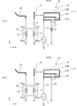
- FIG. 1A is a circuit diagram of an antenna device 101A according to the first embodiment.
- FIG. 1B is a circuit diagram of the antenna device 101B according to the first embodiment.
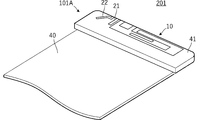
- FIG. 2A is a plan view of a main part of an electronic device 201 including the antenna device 101A, and FIG. 2B is a side view thereof.
- FIG. 2C is a schematic circuit diagram of the antenna device 101 ⁇ / b> A formed on the circuit board 40.
- FIG. 3 is a perspective view of an electronic device including the antenna device 101A.
- FIG. 4 is a cross-sectional view of an electronic device 201 including the antenna device 101A.
- FIG. 5 is a perspective view of the coupling element 30.
- FIG. 1A is a circuit diagram of an antenna device 101A according to the first embodiment.
- FIG. 1B is a circuit diagram of the antenna device 101B according to the first embodiment.
- FIG. 2A is a plan view of a main part of an electronic device 201 including the antenna device 101A
- FIG. 6 is an exploded plan view showing a conductor pattern formed on each layer of the coupling element 30.
- FIG. 7 is a circuit diagram of a coupling element 30 including four coil conductor patterns.
- FIG. 8 is a diagram illustrating a frequency characteristic of a reflection coefficient of the antenna device 101A.
- FIG. 9 is a circuit diagram of the antenna device 102 according to the second embodiment.
- FIG. 10A is a plan view of a main part of an electronic device 202 including the antenna device 102, and FIG. 10B is a side view thereof.
- FIG. 11 is a circuit diagram of an antenna device 103 according to the third embodiment.
- FIG. 12 is a circuit diagram of an antenna device 104 according to the fourth embodiment.
- FIG. 13 is a diagram illustrating a frequency characteristic of a reflection coefficient of the antenna device 104.
- FIG. 14 is a circuit diagram of an antenna device as a comparative example.
- An antenna device includes: A coupling element including a first coil and a second coil coupled to the first coil; A first parasitic radiating element and a second parasitic radiating element that are indirectly fed from the feeding circuit, and a feeding radiating element that is directly fed from the feeding circuit; The first coil is connected between the first parasitic radiation element and ground; The second coil is connected between the second parasitic radiation element and ground; The first parasitic radiation element is electrically coupled to the feed radiation element.
- the feed radiating element and the first parasitic radiating element can be strongly coupled to the electric field, and the second parasitic radiating element is coupled to the first parasitic radiating element via the coupling element.
- the characteristic of the second parasitic radiation element as a radiation element is effectively used. Therefore, a broadband antenna device can be obtained.
- the first coupling element is an element in which a plurality of insulating base materials and a plurality of conductor patterns are stacked, and the plurality of conductor patterns are the plurality of insulating patterns.
- the first coil and the second coil are formed on a surface of a base material, and are formed by one or more conductor patterns among the plurality of conductor patterns. According to this structure, a small first coupling element having a high coupling coefficient is formed, and a small antenna device can be obtained.
- the antenna device includes a portion where the feed radiating element and the first parasitic radiating element extend in the same direction. According to this structure, the coupling between the feed radiation element and the first parasitic radiation element can be enhanced.
- the feed radiating element resonates in a first frequency band and a second frequency band higher in frequency than the first frequency band, and the first parasitic radiation is provided.
- the element and the second parasitic radiation element resonate in the second frequency band. According to this structure, the second frequency band can be widened.
- the resonance frequency of the second parasitic radiating element is the difference between the resonance frequency of the feed radiating element in the second frequency band and the resonance frequency of the first parasitic radiating element. between. According to this structure, the second frequency band having a high frequency band can be effectively widened.
- the feed radiating element, the first parasitic radiating element, and the second parasitic radiating element are formed so as to be arranged in a plane, and the first parasitic radiating element is provided. Is located between the feed radiating element and the second parasitic radiating element. According to this structure, since the radiation efficiency of the second parasitic radiation element is higher than that of the first parasitic radiation element, the resonance frequency in the second frequency band of the feed radiation element and the resonance frequency of the first parasitic radiation element are different. , And the second frequency band is effectively widened.
- the ground is a ground conductor
- the feed radiating element is arranged at a position farther from the ground conductor than the first parasitic radiating element. According to this structure, the radiation efficiency of the long feed line radiating element connected to the feed circuit is increased.
- the feed radiating element is an inverted-F radiating element having a feed line and a short-circuit line. According to this structure, it is possible to obtain an antenna device having a feed radiating element having high radiation efficiency while being small.
- the antenna device includes an inductor connected in series between a short-circuit line of the inverted F-type radiating element and a ground. According to this structure, it is possible to obtain an antenna device that has a feed radiating element that is small and that supports low-band communication.
- the antenna device has a portion extending from a connection portion of a feeder line to the inverted F-type radiating element in a direction away from the first parasitic radiating element. According to this structure, the influence of the first parasitic radiation element on the feed radiation element is small, and the magnetic field coupling between the first parasitic radiation element and the feed radiation element can be enhanced.
- the feed radiating element is connected between the feed circuit and a ground, and the first parasitic radiating element and the second parasitic radiating element are connected to the feed radiating element. Is partially enclosed. According to this structure, the first parasitic radiation element and the second parasitic radiation element can be arranged in a limited space together with the feed radiation element, and a small antenna device is configured.
- An antenna apparatus includes an impedance adjustment circuit connected between the feed radiating element and a ground, the resonance frequency of the first parasitic radiating element and the second parasitic radiating element.
- the impedance of the impedance adjustment circuit at the resonance frequency is higher than the impedance of the feed radiating element at the resonance frequency.
- the fed radiation element is substantially equal to the first parasitic radiation element and the second parasitic radiation element. Since there is no influence, the radiation efficiency of the first parasitic radiation element or the second parasitic radiation element alone can be maintained.
- the antenna device includes a capacitor connected in series between the first parasitic radiation element and the first coil. According to this structure, the resonance frequency of the first parasitic radiation element can be set to the predetermined frequency without shortening the line length of the first parasitic radiation element. Therefore, the degree of coupling between the first parasitic radiation element and the feed radiation element can be ensured.
- An antenna device provides a second coupling element including a third coil and a fourth coil coupled to the third coil, and the power supply circuit via the first coupling element and the second coupling element.
- a third parasitic radiating element which is fed by the power supply, the third coil is connected between the second parasitic radiating element and the ground, and the fourth coil is connected to the third parasitic radiating element and the ground. Connected between According to this structure, further broadening of the band can be achieved by the three parasitic radiation elements.
- An electronic apparatus is the electronic apparatus according to any one of the antenna apparatus according to the first aspect to the antenna apparatus according to the twelfth aspect, and the power supply circuit connected to the antenna apparatus. And a housing for accommodating the antenna device and the circuit board. According to this structure, an electronic device including a broadband antenna device can be obtained.
- the feed radiating element, the first parasitic radiating element, and the second parasitic radiating element are formed on a dielectric or insulator covering a part of the circuit board. This is the conductor pattern obtained. According to this structure, it is possible to obtain an electronic device including a space-saving and high-gain antenna device as compared with a structure in which each radiation element is formed on a circuit board.
- the feed radiating element has a shape along an outer edge of the housing. According to this structure, an electronic device including a relatively large-sized feed radiating element is configured without limiting the space inside the housing.
- FIG. 1A is a circuit diagram of an antenna device 101A according to the first embodiment.
- FIG. 1B is a circuit diagram of another antenna device 101B according to the first embodiment.
- the antenna device 101A includes the feed radiating element 10, the first parasitic radiating element 21, the second parasitic radiating element 22, and the coupling element 30.
- the coupling element 30 includes a first coil L1 and a second coil L2 that is electromagnetically coupled (mainly magnetically coupled) to the first coil L1.
- the coupling element 30 is preferably a laminated transformer or chip component in which the first coil L1 and the second coil L2 are laminated.
- the first coil L1 of the coupling element 30 is connected between the first parasitic radiation element 21 and the ground, and the second coil L2 is connected between the second parasitic radiation element 22 and the ground.
- the first parasitic radiation element 21 and the feed radiation element 10 have a portion extending in the same direction, and the first parasitic radiation element 21 is electrically coupled to the feed radiation element 10 at the extending portion. Arrow lines at both ends in FIGS. 1A and 1B illustrate this electric field coupling.
- the portion where the first parasitic radiation element 21 and the feed radiation element 10 extend in the same direction is a part where the first parasitic radiation element 21 and the feed radiation element 10 run in parallel at an interval from each other.
- the feed radiating element 10 is an inverted-F radiating element including a main radiating element 11, a sub-radiating element 12, a feed line 13, and a short-circuit line 14.
- the power supply circuit 1 is connected between the power supply line 13 and the ground.
- An inductor Ls is connected in series between the short-circuit line 14 and the ground.
- the main radiating element 11 includes a first extending portion 11A extending in the Y direction, and a first extending portion 11A extending from the end of the first extending portion 11A in the X direction.
- a second extending portion 11B that extends, a third extending portion 11C that extends in the ⁇ Y direction from an end of the second extending portion 11B, and a fourth extending portion 11D that extends in the ⁇ X direction from an end of the third extending portion 11C. It consists of.
- the sub radiating element 12 extends in the X direction from the middle of the first extending part 11A of the main radiating element 11, and is disposed between the second extending part 11B and the fourth extending part 11D of the main radiating element 11.
- a stray capacitance Cs is formed between the vicinity of the tip of the sub-radiating element 12 and the vicinity of the tip of the main radiating element 11 (near the tip of the fourth extension 11D).
- the stray capacitance Cs is a capacitance generated between the conductor pattern forming the main radiating element 11 and the conductor pattern forming the sub-radiating element 12.
- This stray capacitance is a capacitance component added to the radiating element of the inverted-F antenna, and the resonance frequency of the main radiating element 11 and the sub-radiating element 12 is adjusted by the magnitude of the stray capacitance.
- the antenna device 101A includes a capacitor C connected in series between the first parasitic radiation element 21 and the first coil L1 of the coupling element 30.
- the capacitor C is provided to increase the resonance frequency of the first parasitic radiation element 21 to a predetermined frequency while maintaining the first parasitic radiation element 21 at a predetermined length.
- the first parasitic radiation element 21 for the high band does not become extremely short, so that the coupling between the first parasitic radiation element 21 and the radiation element 10 can be enhanced.
- the capacitor C may be omitted.
- the feed radiating element 10 is fed directly from the feed circuit 1.
- the first parasitic radiating element 21 is fed by electric field coupling with the feeding radiating element 10, particularly with the main radiating element 11.
- the second parasitic radiation element 22 is fed from the first parasitic radiation element 21 via the coupling element 30.
- the name of the “parasitic radiating element” is a radiating element that is not directly supplied with power from the power supply circuit 1, and is supplied indirectly as described above.
- the inductor Ls makes it difficult for a high-frequency high-frequency current in the communication frequency band to flow from the short-circuit line 14 to the ground side. Thereby, the vicinity of the electric field coupling of the first parasitic radiation element 21 is prevented from being equivalently short-circuited, and the first parasitic radiation element 21 and the feed radiation element 10 are compared with the case where the inductor Ls is not provided. Electric field coupling works more effectively. However, for example, when the electric field coupling between the first parasitic radiation element 21 and the feed radiation element 10 does not matter, the inductor Ls may not be provided as in the antenna device 101B shown in FIG. 1B.
- FIG. 2A is a plan view of a main part of an electronic device 201 including the antenna device 101A
- FIG. 2B is a side view thereof
- FIG. 2C is an antenna formed on the circuit board 40.
- FIG. 3 is a perspective view of a main part of an electronic device including the antenna device 101A.
- FIG. 4 is a cross-sectional view of an electronic device 201 including the antenna device 101A.
- the electronic device 201 includes an antenna device 101A, a circuit board 40 on which a power supply circuit connected to the antenna device 101A is formed, a housing 50 that houses the antenna device 101A and the circuit board 40, Is provided.
- the circuit board 40 includes a ground conductor formation region GR and a ground conductor non-formation region NGR.
- the antenna 41 is disposed at a position covering the non-ground conductor forming region NGR of the circuit board 40.
- the antenna 41 has a predetermined conductor pattern formed on a dielectric or an insulator.
- the feed radiating element 10 On the surface of the antenna 41, the feed radiating element 10, the first parasitic radiating element 21, and the second parasitic radiating element 22 are formed.
- the surface of the antenna 41 is a radiating element forming region. The smallest rectangular area surrounding a plurality of radiating elements formed in a plane may be the radiating element forming area.
- the feed radiating element 10, the first parasitic radiating element 21, and the second parasitic radiating element 22 are formed so as to be arranged in a plane direction. It is located at a position sandwiched by the feed radiating element 22. Therefore, the feed radiating element 10 and the second parasitic radiating element 22 are located outside the radiating element forming region with respect to the first parasitic radiating element 21.
- the feed radiating element 10, the first parasitic radiating element 21, and the second parasitic radiating element 22 are, for example, conductive patterns of Cu or the like formed by the LDS method (Laser Direct Structuring).
- an electronic device including an antenna device that is space-saving and has a high gain as compared with a structure in which each radiation element is formed on the circuit board 40.
- the main radiating element 11 Since the stray capacitance Cs shown in FIGS. 1A and 1B is generated between the conductor pattern forming the main radiating element 11 and the conductor pattern forming the sub-radiating element 12, the main radiating element 11 is The size of the stray capacitance Cs can be adjusted by trimming the open end of the conductor pattern forming the conductor pattern or the conductor pattern forming the auxiliary radiation element 12.
- the power supply circuit 1 shown in FIGS. 1A, 1B, and 2C is formed on the circuit board 40. Further, the coupling element 30, the inductor Ls, and the capacitor C are formed on the circuit board 40. (In the example shown in FIG. 2C, the chip capacitor C and the chip inductor Ls are mounted.)
- the coupling element 30 is a chip component (transformer of a laminated body) including the first coil L1 and the second coil L2. It is mounted on a circuit board 40.
- the antenna 41 is mounted on the circuit board 40, and the feed radiating element 10 formed on the antenna 41 is electrically connected to one end of the feed circuit 1. Connected to one end of chip inductor Ls.
- the first parasitic radiation element 21 is connected to one end of the chip capacitor C, and the second parasitic radiation element 22 is connected to the second parasitic radiation element connection terminal PS2 of the coupling element 30 (FIGS. 1A and 1B). B)).
- the second parasitic radiation element 22 extends non-parallel to the first parasitic radiation element 21. Therefore, the second parasitic radiation element 22 is mainly magnetically coupled to the first parasitic radiation element 21 via the coupling element 30 without performing unnecessary electric field coupling.
- the feed radiating element 10 is an inverted F-type radiating element, an antenna device having a small size but having a high radiation efficiency can be obtained.
- the inductor Ls connected in series between the short-circuit line 14 of the inverted F-type radiating element and the ground is provided, the power-supplying radiating element is small in size and compatible with communication in a low frequency band (for example, a low band described later). Is obtained.
- 2A and 2C show an example in which a conductor pattern is not formed between the power supply line 13 and the short-circuit line 14, but a conductor pattern is formed in this portion. You may. That is, a continuous conductor pattern from the power supply line 13 to the short-circuit line 14 may be formed.
- the second extending portion 11B extending in the direction away from the first parasitic radiation element 21 from the connection portion of the feed line 13 to the inverted F-type radiation element is provided, Since most of the radiation that contributes to the radiation is located at a position distant from the first parasitic radiation element 21, it is possible to suppress the radiation of the feed radiation element 10 from being hindered by the first parasitic radiation element 21. In other words, the influence of the first parasitic radiation element 21 on the feed radiation element 10 is small. Since the second parasitic radiation element 22 is located farther from the feed radiation element 10 than the first parasitic radiation element 21, the influence on the feed radiation element 10 is further reduced. Thereby, the radiation characteristics of the first parasitic radiation element 21 and the second parasitic radiation element 22 can be added to the radiation characteristic of the feed radiation element 10 without substantially changing the radiation characteristic of the feed radiation element 10.
- FIG. 14 shows a circuit diagram of an antenna device as a comparative example.
- the antenna device as the comparative example includes a feed radiating element 60, a first parasitic radiating element 71, a second parasitic radiating element 72, and a coupling element 80.
- the first coil LA of the coupling element 80 is connected between the feed radiating element 60 and the ground
- the second coil LB is connected between the first parasitic radiating element 71 and the ground.
- the second parasitic radiation element 72 is arranged close to the first parasitic radiation element 71 for electric field coupling.
- the antenna device of the comparative example as shown in FIG. 14 it is not possible to strongly couple a further parasitic radiation element (second parasitic radiation element 72) to the parasitic radiation element (first parasitic radiation element 71). It is difficult for the additional parasitic radiation element (second parasitic radiation element 72) to receive sufficient power from the parasitic radiation element (first parasitic radiation element 71). Therefore, the effect of widening the band by adding the second parasitic radiation element 72 is small.
- the first parasitic radiating element 71 changes the radiation characteristic of the feed radiating element 60.
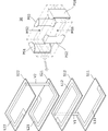
- FIG. 5 is a perspective view of the coupling element 30, and FIG. 6 is an exploded plan view showing a conductor pattern formed on each layer of the coupling element 30.
- the coupling element 30 of the present embodiment is a rectangular parallelepiped chip component mounted on a circuit board in an electronic device.
- FIG. 5 the external shape of the coupling element 30 and the internal structure are separately illustrated.
- the outer shape of the coupling element 30 is represented by a two-dot chain line.
- a first ground terminal PG1, a first parasitic radiation element connection terminal PS1, a second ground terminal PG2, and a second parasitic radiation element connection terminal PS2 are formed on the outer surface of the coupling element 30, a first ground terminal PG1, a first parasitic radiation element connection terminal PS1, a second ground terminal PG2, and a second parasitic radiation element connection terminal PS2 are formed.
- the coupling element 30 includes a first surface MS1 and a second surface MS2 opposite to the first surface.
- the first surface MS1 is a mounting surface, and this surface faces the circuit board.
- first conductor pattern L11, a second conductor pattern L12, a third conductor pattern L21, and a fourth conductor pattern L22 are formed inside the coupling element 30.
- the first conductor pattern L11 and the second conductor pattern L12 are connected via an interlayer connection conductor V1.
- the third conductor pattern L21 and the fourth conductor pattern L22 are connected via an interlayer connection conductor V2.
- the insulating base materials S11, S12, S21, and S22 on which the above-described conductor patterns are formed are separately illustrated in the stacking direction.
- the first ground terminal PG1 and the first parasitic radiation element connection terminal PS1 are terminals to which both ends of the first coil L1 are connected, and the first parasitic radiation element connection terminal PS1 and the second ground terminal PG2 are connected to the second coil. Both ends are connected terminals.
- a pattern L22 is formed.
- These coil conductor patterns are arranged such that the first conductor pattern L11, the second conductor pattern L12, the third conductor pattern L21, and the fourth conductor pattern L22 are arranged in this order from the layer closest to the mounting surface. S21 and S22 are stacked.
- FIG. 6 shows an insulating substrate on which a coil conductor pattern is formed.
- a plurality of insulating bases on which no coil conductor pattern is formed are stacked below the insulating base S11 and above the insulating base S22.
- the first end of the first conductor pattern L11 is connected to the first ground terminal PG1, and the second end is connected to the first end of the second conductor pattern L12 via the interlayer connection conductor V1.
- the second end of the second conductor pattern L12 is connected to the first parasitic radiation element connection terminal PS1.
- the first end of the third conductor pattern L21 is connected to the second parasitic radiation element connection terminal PS2, and the second end of the third conductor pattern L21 is connected to the fourth conductor pattern L22 via the interlayer connection conductor V2. It is connected to the first end.
- the second end of the fourth conductor pattern L22 is connected to the second ground terminal PG2.
- the insulating bases S11, S12, S21, and S22 are, for example, liquid crystal polymer (LCP) sheets, and the conductor patterns L11, L12, L21, and L22 are formed by patterning copper foil, for example. It was done.
- the insulating base materials S11, S12, S21, and S22 are, for example, low-temperature co-fired ceramics (LTCC [Low Temperature Co-fired Ceramics]) and have conductor patterns L11 and L12. , L21 and L22 are formed by printing a copper paste, for example.
- FIG. 7 is a circuit diagram of the coupling element 30 including the four coil conductor patterns.
- the second conductor pattern L12 and the first conductor pattern L11 are connected in series to form a first coil L1.
- the fourth conductor pattern L22 and the third conductor pattern L21 are connected in series to form a second coil L2.
- the first coil L1 and the second coil L2 are electromagnetically coupled.
- the conductor patterns L11, L12, L21, and L22 overlap over the entire circumference in plan view, and the conductor patterns L11, L12, L21, and L22 are closest to each other in the stacking direction (other insulating base materials). ), And the coupling coefficient between the first coil L1 and the second coil L2 is high.
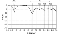
- FIG. 8 is a diagram showing the frequency characteristic of the reflection coefficient of the antenna device 101A.
- the horizontal axis represents the frequency
- the vertical axis represents the reflection loss (S11) of the antenna device 101A viewed from the power supply circuit 1.
- resonance points occur at frequencies f11, f12, f21, and f22.
- the frequency f11 is a resonance frequency of the main radiation element 11 in the first frequency band F1
- the frequency f12 is a resonance frequency of the sub radiation element 12.
- This frequency f12 is a resonance frequency in a second frequency band F2 having a higher frequency than the first frequency band.
- the frequency f21 is the resonance frequency of the first parasitic radiation element 21
- the frequency f22 is the resonance frequency of the second parasitic radiation element 22.
- the first frequency band F1 is a low-band communication frequency band from 700 MHz to 960 MHz, for example
- the second frequency band F2 is a high-band communication frequency band from 1700 MHz to 2700 MHz, for example.
- the resonance of the main radiating element 11 is used for low-band communication
- the resonance of the sub-radiating element 12 is used for high-band communication such as the 1800 MHz band.
- the resonance of the resonance frequency f22 of the second parasitic radiation element 22 and the resonance of the resonance frequency f21 of the first parasitic radiation element 21 are used for high-band communication higher than f12.
- the feed radiating element 10 has a resonance frequency in both the first frequency band F1 and the second frequency band F2, and the first parasitic radiating element 21 and the second parasitic radiating element 22 are in the second frequency band F2. Has a resonance frequency.
- the resonance frequency f22 of the second parasitic radiation element 22 is determined between the resonance frequency f21 of the first parasitic radiation element 21 and the resonance frequency f12 in the second frequency band of the feed radiation element 10. Therefore, the resonance frequency of the first parasitic radiation element 21 from the resonance frequency of the feed radiation element 10 (particularly, in this embodiment, the resonance frequency f12 of the auxiliary radiation element 12, that is, the resonance frequency in the second frequency band of the feed radiation element 10).
- the antenna devices 101A and 101B can be used over a wide band continuous up to f21.
- the second parasitic radiation element 22 is located outside (in a position electrically separated from the power supply circuit 1) in the radiating element forming region than the first parasitic radiation element 21, so that the radiation is not easily disturbed. Therefore, the second parasitic radiation element 22 effectively contributes to broadening the band.
- a higher-order resonance mode such as 3 ⁇ / 4 resonance may be used.
- a high-frequency band can be similarly widened for an inverted F-type radiating element in which the feeding radiating element does not include the auxiliary radiating element.
- FIG. 9 is a circuit diagram of the antenna device 102 according to the second embodiment.
- the antenna device 102 includes a first parasitic radiation element 21, a second parasitic radiation element 22, a radiation element 10, and a coupling element 30.
- the first coil L1 of the coupling element 30 is connected between the first parasitic radiation element 21 and the ground, and the second coil L2 is connected between the second parasitic radiation element 22 and the ground.
- the first parasitic radiating element 21 and the feeding radiating element 10 have their tips close to each other.
- the tip of the first parasitic radiation element 21 and the tip of the feed radiation element 10 extend in the same direction.
- the direction in which the feeding radiating element 10 extends from the connection portion (feeding point) of the feeding line and the direction in which the first parasitic radiating element 21 extends from the coupling element 30 are opposite to each other.
- the first parasitic radiating element 21 and the feeding radiating element 10 are electrically coupled mainly at a portion where the tips are close to each other (a portion surrounded by a broken line in the drawing).
- the feed radiating element 10 is fed directly from the feed circuit 1.
- the first parasitic radiation element 21 is fed by electric field coupling with the feed radiation element 10.
- the second parasitic radiation element 22 is fed from the first parasitic radiation element 21 via the coupling element 30.
- the feed radiating element 10 is used for communication in a first frequency band (for example, low band from 700 MHz to 960 MHz) by its quarter wavelength resonance, and is used for communication in a second frequency band (for example, from 1700 MHz to 2700 MHz) by its quarter wavelength resonance. Band).
- the resonance of the first parasitic radiation element 21 and the resonance of the second parasitic radiation element 22 are used for communication in the second frequency band.
- the distal end of the feed radiating element 10 (the end farther from the connection part of the feeder line) and the distal end of the first parasitic radiating element 21 are portions having a high electric field strength, and therefore, the first parasitic radiating element 21 is not. Even if the parallel running distance between the tip of the radiating element 21 and the tip of the feeding radiating element 10 is short, the feeding radiating element 10 and the first parasitic radiating element 21 can be strongly coupled.
- FIG. 10A is a plan view of a main part of an electronic device 202 including the antenna device 102
- FIG. 10B is a side view thereof.
- the electronic device 202 includes the antenna device 102, a circuit board 40 on which a power supply circuit connected to the antenna device 102 is formed, and a housing that houses the antenna device 102 and the circuit board 40.
- the housing is not shown in FIGS. 10A and 10B.
- the circuit board 40 includes a ground conductor forming region GR and a ground conductor non-forming region NGR.
- the antenna 41 is disposed at a position covering the non-ground conductor forming region NGR of the circuit board 40.
- the antenna 41 has a predetermined conductor pattern formed on a dielectric or an insulator.
- the feed radiating element 10, the first parasitic radiating element 21, and the second parasitic radiating element 22 are formed on the surface of the antenna 41.
- the feed radiating element 10, the first parasitic radiating element 21, and the second parasitic radiating element 22 are, for example, conductive patterns of Cu or the like formed by the LDS method (Laser Direct Structuring).
- the power supply circuit 1 shown in FIG. 9 is formed on the circuit board 40. Further, the coupling element 30 is formed on the circuit board 40.
- the coupling element 30 is a chip component including the first coil L1 and the second coil L2, and is mounted on the circuit board 40.
- the feed radiating element 10 formed on the antenna 41 is connected to one end of the feed circuit 1 while the antenna 41 is mounted on the circuit board 40 and is electrically connected.
- the first parasitic radiation element 21 and the second parasitic radiation element 22 are connected to the coupling element 30.
- the second parasitic radiating element 22 It is located outside the feed radiating element 21. According to this structure, since the radiation efficiency of the second parasitic radiation element 22 is higher than that of the first parasitic radiation element 21, the resonance frequency in the second frequency band of the passive radiation element 10 and the first parasitic radiation element 21 The gain in the frequency band between the first and second resonance frequencies is increased, and the second frequency band is effectively widened.
- the feed radiating element 10 is arranged at a position farther from the ground conductor forming region GR than the first parasitic radiating element 21. According to this structure, the radiation efficiency of the feed radiating element 10 having a long line length connected to the feed circuit 1 is increased.
- FIG. 11 is a circuit diagram of an antenna device 103 according to the third embodiment.
- This antenna device 103 includes a first parasitic radiation element 21, a second parasitic radiation element 22, a radiation element 10, and a coupling element 30.
- the feed radiating element 10 has an end opposite to the connection end of the feed circuit 1 connected to the ground via the impedance adjusting circuit 15. Since the feeding radiating element 10, the impedance adjusting circuit 15, the ground, and the feeding circuit 1 form a loop, the feeding radiating element 10 can be called a loop radiating element.
- the feed radiation element 10 is formed at a position surrounding the first parasitic radiation element 21 and the second parasitic radiation element 22.
- the first parasitic radiation element 21 and the feed radiation element 10 have a part extending in the same direction (a part where the first parasitic radiation element 21 and the feed radiation element 10 run in parallel).
- the first parasitic radiation element 21 is electrically coupled to the feed radiation element 10.
- the feed radiating element 10 is fed directly from the feed circuit 1.
- the first parasitic radiating element 21 is fed by electric field coupling with the feeding radiating element 10, particularly with the main radiating element 11.
- the second parasitic radiation element 22 is fed from the first parasitic radiation element 21 via the coupling element 30.
- the feed radiating element 10 is used for communication in a first frequency band (for example, a low band from 700 MHz to 960 MHz), and the first parasitic radiating element 21 and the second parasitic radiating element 22 are in a second frequency band (for example, from 1700 MHz to 2700 MHz). Used for high-band) communications.
- a first frequency band for example, a low band from 700 MHz to 960 MHz
- the first parasitic radiating element 21 and the second parasitic radiating element 22 are in a second frequency band (for example, from 1700 MHz to 2700 MHz). Used for high-band) communications.
- the impedance adjusting circuit 15 has a high impedance in a high band, and the tip of the feed radiating element 10 (end farther from the connection of the feed circuit 1) is substantially open. In other words, the reactance of the impedance adjustment circuit 15 is determined so that the tip of the feed radiating element 10 is substantially open in the high band. For this reason, in the high band, the first parasitic radiation element 21 and the second parasitic radiation element 22 are not electrically surrounded by the loop. In other words, when the first parasitic radiation element 21 and the second parasitic radiation element 22 radiate, the feed radiating element 10 appears to be open by the impedance adjustment circuit 15. Therefore, in the high band, the first parasitic radiation element 21 and the second parasitic radiation element 22 function as radiation elements without being affected by the radiation element 10. That is, the radiation efficiency of the first parasitic radiation element 21 or the second parasitic radiation element 22 alone is maintained.
- the feed radiation element 10 is connected between the feed circuit 1 and the ground, and the first parasitic radiation element 21 and the second parasitic radiation element 22 are partially surrounded by the feed radiation element 10. Therefore, the first parasitic radiation element 21 and the second parasitic radiation element 22 can be arranged in a limited space together with the feed radiation element 10, and a small antenna device is configured.
- FIG. 12 is a circuit diagram of an antenna device 104 according to the fourth embodiment.
- This antenna device 104 includes a feed radiating element 10, a first parasitic radiating element 21, a second parasitic radiating element 22, a third parasitic radiating element 23, and coupling elements 30A and 30B.
- the antenna device 104 of the present embodiment includes a third parasitic radiation element 23 and two coupling elements 30A and 30B, different from the examples shown in FIGS. 1A and 1B.
- the coupling element 30A includes a first coil L1, and a second coil L2 that is electromagnetically coupled (mainly magnetically coupled) to the first coil L1.
- the coupling element 30B includes a third coil L3 and a fourth coil L4 that is electromagnetically coupled (mainly magnetically coupled) to the third coil L3.
- the first coil L1 of the coupling element 30A is connected between the first parasitic radiation element 21 and the ground.
- a series circuit of the second coil L2 of the coupling element 30A and the third coil L3 of the coupling element 30B is connected between the second parasitic radiation element 22 and the ground.
- the fourth coil L4 of the coupling element 30B is connected between the third parasitic radiation element 23 and the ground.
- the feed radiating element 10 is an inverted-F radiating element including a main radiating element 11, a sub-radiating element 12, a feed line 13, and a short-circuit line 14.
- the power supply circuit 1 is connected between the power supply line 13 and the ground via a capacitor C.
- An inductor Ls is connected in series between the short-circuit line 14 and the ground.
- the configuration of the feed radiating element 10 is as described in the first embodiment. Further, the configuration of the first parasitic radiation element 21 and the second parasitic radiation element 22 is the same as the first parasitic radiation element 21 and the second parasitic radiation element 22 shown in the first embodiment.
- FIG. 13 is a diagram showing the frequency characteristic of the reflection coefficient of the antenna device 104.
- the horizontal axis represents the frequency
- the vertical axis represents the reflection loss (S11) of the antenna device 104 as viewed from the power supply circuit 1.
- resonance points occur at frequencies f11, f12, f21, f22, and f23.
- the frequency f11 is the resonance frequency of the main radiating element 11 in the first frequency band F1
- the frequency f12 is the resonance frequency of the sub-radiating element 12.
- This frequency f12 is a resonance frequency in a second frequency band F2 having a higher frequency than the first frequency band.
- the frequency f21 is the resonance frequency of the first parasitic radiation element 21
- the frequency f22 is the resonance frequency of the second parasitic radiation element 22
- the frequency f23 is the resonance frequency of the third parasitic radiation element 23.
- the first frequency band F1 is a low-band communication frequency band from 700 MHz to 960 MHz, for example
- the second frequency band F2 is a high-band communication frequency band from 1700 MHz to 2700 MHz, for example.
- the resonance of the main radiating element 11 is used for low-band communication
- the resonance of the sub-radiating element 12 is used for high-band communication such as the 1800 MHz band.
- the resonance of the first parasitic radiation element 21 at the resonance frequency f21, the resonance of the second parasitic radiation element 22 at the resonance frequency f22, and the resonance of the third parasitic radiation element 23 at the resonance frequency f23 are higher than f12. Used for high-band communication in the region.
- the feed radiating element 10 has a resonance frequency in both the first frequency band F1 and the second frequency band F2, and includes the first parasitic radiating element 21, the second parasitic radiating element 22, and the third parasitic radiating element.
- the radiating element 23 has a resonance frequency in the second frequency band F2.
- the antenna device of the present invention can be used not only for transmission but also for reception or transmission / reception, and the same operation is performed even if transmission / reception is reversed.
- the “feeding circuit” is not limited to a circuit that outputs transmission power, but corresponds to a circuit that inputs and amplifies a reception signal during reception.
- the electronic device according to the present invention is not limited to the electronic devices 201 and 202 described above.
- an electronic device including the antenna device described in the third embodiment or the fourth embodiment is also included in the electronic device of the present invention.
- Capacitor GR Ground conductor forming area L1, LA ... First coil L2, LB ... Second coil L3 ... Third coil L4 ... Fourth coil L11 ... First conductor pattern L12 ... Second conductor pattern L21 ... Third conductor Pattern L22 Fourth conductor pattern Ls Inductor MS1 First surface MS2 Second surface NGR Ground conductor non-forming region PG1 First ground terminal PG2 Second ground terminal PS1 First parasitic radiation element connection terminal PS2 ... second parasitic radiation element connection terminals S11, S12, S21, S22 ... insulating bases V1, V2 ... interlayer connection conductor 1 ... power supply circuits 10, 60 ... power supply radiation elements 11, 71 ... main radiation element 11A ...
- first extension Portion 11B Second extension portion 11C Third extension portion 11D Fourth extension portion 12, 72 Secondary radiating element 13 Feeding line 14
- Short circuit line 15 Impedance adjustment Path 21 first parasitic radiation element 22 second parasitic radiation element 30, 30A, 30B, 80 coupling element 40 circuit board 41 antenna 50 housings 101A, 101B, 102, 103, 104 antenna apparatus 201, 202 ...
Landscapes
- Support Of Aerials (AREA)
- Details Of Aerials (AREA)
Abstract
アンテナ装置(101A,101B)は、第1コイル(L1)と、第1コイル(L1)に結合する第2コイル(L2)とを備える結合素子(30)と、給電放射素子(10)と、第1無給電放射素子(21)と、第2無給電放射素子(22)とを備える。そして、第1コイル(L1)は第1無給電放射素子(21)とグランドとの間に接続され、第2コイル(L2)は第2無給電放射素子(22)とグランドとの間に接続され、第1無給電放射素子(21)は給電放射素子(10)に電界結合する。
Description
本発明は、アンテナ装置及びそれを備える電子機器に関するものである。
アンテナ装置を備える携帯電子機器においては、携帯可能な、限られた大きさの筐体内に電子回路と共にアンテナ装置が設けられる。そのため、筐体内に収まる回路基板の大きさ及びアンテナ装置の大きさには自ずと制約がある。
一方、通信に用いる周波数帯域の広帯域化が進んでいるが、上述のとおり、アンテナを設けるスペースに余裕がなく、複数の周波数帯域をカバーするために多数のアンテナを設けることが困難な状況になっている。
アンテナ装置の放射利得の周波数特性を広帯域化する一つの方法として、給電回路から物理的に切り離された無給電放射素子を給電放射素子に磁界結合させることによって、無給電放射素子の特性を給電放射素子の特性に付加する手法が従来用いられている。
例えば、特許文献1には、2つの放射素子と、この2つの放射素子に対する給電を制御する結合度調整回路とを備えたアンテナ装置が示されている。
ところが、近年の更なる広帯域の通信に適用可能なアンテナ装置を構成するために、上述の、無給電放射素子を付加する手法を適用できない。例えば、給電放射素子に結合する無給電放射素子に更に別の無給電放射素子を近接配置しても広帯域化の効果は小さい。これは、新たに追加する無給電放射素子が、既に設けられている無給電放射素子から充分な電力を受けられないからである。
本発明の目的は、給電放射素子と無給電放射素子とを備えて、効果的に広帯域化を図ったアンテナ装置及びそれを備える電子機器を提供することにある。
本開示の一例としてのアンテナ装置は、
第1コイル及び当該第1コイルに結合する第2コイルを備える第1結合素子と、給電回路と、給電放射素子と、第1無給電放射素子と、第2無給電放射素子と、を備え、
前記給電放射素子は、前記給電回路に接続され、前記第1コイルは前記第1無給電放射素子とグランドとの間に接続され、前記第2コイルは前記第2無給電放射素子とグランドとの間に接続され、
前記第1無給電放射素子は前記給電放射素子と電界結合することによって給電され、前記第2無給電放射素子は前記第1結合素子を介して給電される。
第1コイル及び当該第1コイルに結合する第2コイルを備える第1結合素子と、給電回路と、給電放射素子と、第1無給電放射素子と、第2無給電放射素子と、を備え、
前記給電放射素子は、前記給電回路に接続され、前記第1コイルは前記第1無給電放射素子とグランドとの間に接続され、前記第2コイルは前記第2無給電放射素子とグランドとの間に接続され、
前記第1無給電放射素子は前記給電放射素子と電界結合することによって給電され、前記第2無給電放射素子は前記第1結合素子を介して給電される。
上記構成によれば、給電放射素子と第1無給電放射素子とを強く電界結合させることができ、かつ、第2無給電放射素子は結合素子を介して第1無給電放射素子と結合するので、第2無給電放射素子の放射素子としての特性が有効に利用される。そのため、広帯域のアンテナ装置が得られる。
本開示の一例としての電子機器は、上記アンテナ装置と、当該アンテナ装置に接続される給電回路が形成された回路基板と、前記アンテナ装置及び前記回路基板を収める筐体と、を備える。
上記構成により、筐体内の限られたスペースに設けられたアンテナ装置を備える電子機器が得られる。
本発明によれば、給電放射素子と無給電放射素子とを備える広帯域のアンテナ装置、及びそれを備える電子機器が得られる。
まず、本発明に係るアンテナ装置及び電子機器における各種態様の構成について記載する。
本発明に係る第1の態様のアンテナ装置は、
第1コイル及び当該第1コイルに結合する第2コイルを備える結合素子と、
給電回路から間接的に給電される第1無給電放射素子及び第2無給電放射素子並びに前記給電回路から直接的に給電される給電放射素子と、を備え、
前記第1コイルは前記第1無給電放射素子とグランドとの間に接続され、
前記第2コイルは前記第2無給電放射素子とグランドとの間に接続され、
前記第1無給電放射素子は前記給電放射素子に電界結合する。
第1コイル及び当該第1コイルに結合する第2コイルを備える結合素子と、
給電回路から間接的に給電される第1無給電放射素子及び第2無給電放射素子並びに前記給電回路から直接的に給電される給電放射素子と、を備え、
前記第1コイルは前記第1無給電放射素子とグランドとの間に接続され、
前記第2コイルは前記第2無給電放射素子とグランドとの間に接続され、
前記第1無給電放射素子は前記給電放射素子に電界結合する。
上記構成によれば、給電放射素子と第1無給電放射素子とを強く電界結合させることができ、かつ、第2無給電放射素子は結合素子を介して第1無給電放射素子と結合するので、第2無給電放射素子の放射素子としての特性が有効に利用される。そのため、広帯域のアンテナ装置が得られる。
本発明に係る第2の態様のアンテナ装置では、前記第1結合素子は、複数の絶縁基材と、複数の導体パターンとが積層された素子であり、前記複数の導体パターンは前記複数の絶縁基材の表面に形成され、前記第1コイル及び前記第2コイルは、前記複数の導体パターンのうち、1つ以上の導体パターンによって形成される。この構造によれば、結合係数の高い小型の第1結合素子が構成され、小型のアンテナ装置が得られる。
本発明に係る第3の態様のアンテナ装置は、前記給電放射素子及び前記第1無給電放射素子が、互いに同方向に延伸する部分を有する。この構造によれば、給電放射素子と第1無給電放射素子との結合を高めることができる。
本発明に係る第4の態様のアンテナ装置は、前記給電放射素子が、第1周波数帯域と、前記第1周波数帯域よりも周波数の高い第2周波数帯域とで共振し、前記第1無給電放射素子及び前記第2無給電放射素子は前記第2周波数帯域で共振する。この構造によれば、第2周波数帯域を広帯域化できる。
本発明に係る第5の態様のアンテナ装置は、前記第2無給電放射素子の共振周波数が前記給電放射素子の前記第2周波数帯域における共振周波数と前記第1無給電放射素子の共振周波数との間にある。この構造によれば、周波数帯域の高い第2周波数帯域を効果的に広帯域化できる。
本発明に係る第6の態様のアンテナ装置は、前記給電放射素子、前記第1無給電放射素子及び前記第2無給電放射素子は平面方向に並ぶように形成され、前記第1無給電放射素子は前記給電放射素子と前記第2無給電放射素子とで挟まれる位置にある。この構造によれば、第1無給電放射素子に比べて第2無給電放射素子の放射効率が高まるので、給電放射素子の第2周波数帯域における共振周波数と第1無給電放射素子の共振周波数との間の利得が高まり、第2周波数帯域が効果的に広帯域化される。
本発明に係る第7の態様のアンテナ装置は、前記グランドはグランド導体であり、前記給電放射素子が前記第1無給電放射素子に比べてグランド導体から離れた位置に配置されている。この構造によれば、給電回路に接続される線長の長い給電放射素子の放射効率が高まる。
本発明に係る第8の態様のアンテナ装置は、前記給電放射素子が、給電線と短絡線とを有する逆F型放射素子である。この構造によれば、小型でありながら放射効率の高い給電放射素子を有するアンテナ装置が得られる。
本発明に係る第9の態様のアンテナ装置は、前記逆F型放射素子の短絡線とグランドとの間に直列接続されたインダクタを備える。この構造によれば、小型でありながらローバンドでの通信に対応する給電放射素子を有するアンテナ装置が得られる。
本発明に係る第10の態様のアンテナ装置は、前記逆F型放射素子への給電線の接続部から前記第1無給電放射素子より遠ざかる方向に延伸する部分を有する。この構造によれば、第1無給電放射素子が給電放射素子に与える影響は小さく、第1無給電放射素子と給電放射素子との磁界結合を高めることができる。
本発明に係る第11の態様のアンテナ装置は、前記給電放射素子が前記給電回路とグランドとの間に接続され、前記第1無給電放射素子及び前記第2無給電放射素子は前記給電放射素子で部分的に囲まれる。この構造によれば、給電放射素子と共に第1無給電放射素子及び第2無給電放射素子を限られたスペースに配置することができ、小型のアンテナ装置が構成される。
本発明に係る第12の態様のアンテナ装置は、前記給電放射素子とグランドとの間に接続されたインピーダンス調整回路を備え、前記第1無給電放射素子の共振周波数及び前記第2無給電放射素子の共振周波数での前記インピーダンス調整回路のインピーダンスは前記給電放射素子の共振周波数でのインピーダンスより高い。この構造によれば、第1無給電放射素子の共振周波数及び第2無給電放射素子の共振周波数で、給電放射素子は第1無給電放射素子及び第2無給電放射素子に対して実質的に影響を与えないので、第1無給電放射素子又は第2無給電放射素子単体での放射効率が維持できる。
本発明に係る第13の態様のアンテナ装置は、前記第1無給電放射素子と前記第1コイルとの間に直列接続されたキャパシタを備える。この構造によれば、第1無給電放射素子の線長を短くすることなく、第1無給電放射素子の共振周波数を所定周波数に定めることができる。そのため、第1無給電放射素子と給電放射素子との結合度を確保できる。
本発明に係る第14の態様のアンテナ装置は、第3コイル及び当該第3コイルに結合する第4コイルを備える第2結合素子と、前記給電回路から第1結合素子及び第2結合素子を介して給電される第3無給電放射素子と、を備え、前記第3コイルは前記第2無給電放射素子とグランドとの間に接続され、前記第4コイルは前記第3無給電放射素子とグランドとの間に接続される。この構造によれば、3つの無給電放射素子により、更なる広帯域化が図れる。
本発明に係る第15の態様の電子機器は、上記第1の態様のアンテナ装置から上記第12の態様のアンテナ装置のいずれかに記載のアンテナ装置と、当該アンテナ装置に接続される前記給電回路が形成された回路基板と、前記アンテナ装置及び前記回路基板を収める筐体と、を備える。この構造によれば、広帯域のアンテナ装置を備える電子機器が得られる。
本発明に係る第16の態様の電子機器は、前記給電放射素子、前記第1無給電放射素子及び前記第2無給電放射素子が、前記回路基板の一部を覆う誘電体又は絶縁体に形成された導体パターンである。この構造によれば、回路基板に各放射素子を形成する構造に比べて、省スペースかつ高利得のアンテナ装置を備える電子機器が得られる。
本発明に係る第17の態様の電子機器は、前記給電放射素子が前記筐体の外縁に沿った形状を備える。この構造によれば、筐体内部の空間を制限することなく、相対的に大サイズの給電放射素子を備える電子機器が構成される。
以降、図を参照して幾つかの具体的な例を挙げて、本発明を実施するための複数の形態を示す。各図中には同一箇所に同一符号を付している。要点の説明又は理解の容易性を考慮して、実施形態を説明の便宜上分けて示すが、異なる実施形態で示した構成の部分的な置換又は組み合わせは可能である。第2の実施形態以降では第1の実施形態と共通の事柄についての記述を省略し、異なる点についてのみ説明する。特に、同様の構成による同様の作用効果については実施形態毎には逐次言及しない。
《第1の実施形態》
図1(A)は第1の実施形態に係るアンテナ装置101Aの回路図である。また、図1(B)は第1の実施形態に係る別のアンテナ装置101Bの回路図である。
図1(A)は第1の実施形態に係るアンテナ装置101Aの回路図である。また、図1(B)は第1の実施形態に係る別のアンテナ装置101Bの回路図である。
アンテナ装置101Aは、給電放射素子10と、第1無給電放射素子21と、第2無給電放射素子22と、結合素子30とを備える。
結合素子30は第1コイルL1と、この第1コイルL1に電磁界結合(主として磁界結合)する第2コイルL2とを備える。第1コイルL1と第2コイルL2の結合を高めることを考慮すると、結合素子30は、第1コイルL1と第2コイルL2とを積層した、積層体のトランスやチップ部品であることが好ましい。
結合素子30の第1コイルL1は第1無給電放射素子21とグランドとの間に接続されていて、第2コイルL2は第2無給電放射素子22とグランドとの間に接続されている。
第1無給電放射素子21と給電放射素子10とは同方向に延伸する部分を有し、その延伸する部分で、第1無給電放射素子21は給電放射素子10に電界結合する。図1(A)、図1(B)中の両端矢印線は、この電界結合を図示するものである。なお、第1無給電放射素子21と給電放射素子10とが同方向に延伸する部分は、第1無給電放射素子21と給電放射素子10とが互いに間隔をおいて並走する部分である。
給電放射素子10は、主放射素子11、副放射素子12、給電線13、及び短絡線14を備える逆F型放射素子である。給電線13とグランドとの間には給電回路1が接続される。短絡線14とグランドとの間にはインダクタLsが直列接続されている。
図1(A)、図1(B)に示すX-Y座標軸の採り方において、主放射素子11は、Y方向に延伸する第1延伸部11A、第1延伸部11Aの端からX方向に延伸する第2延伸部11Bと、第2延伸部11Bの端から-Y方向に延伸する第3延伸部11Cと、第3延伸部11Cの端から-X方向に延伸する第4延伸部11Dとで構成される。
副放射素子12は主放射素子11のうち第1延伸部11Aの途中からX方向に延伸し、主放射素子11の第2延伸部11Bと第4延伸部11Dとの間に配置される。そして、この副放射素子12の先端付近と主放射素子11の先端付近(第4延伸部11Dの先端付近)との間に浮遊容量Csを形成している。この浮遊容量Csは主放射素子11を構成する導体パターンと副放射素子12を構成する導体パターンとの間に生じる容量である。この浮遊容量は逆Fアンテナの放射素子に付加される容量成分であり、この浮遊容量の大きさによって主放射素子11及び副放射素子12の共振周波数が調整されている。
アンテナ装置101Aは、第1無給電放射素子21と結合素子30の第1コイルL1との間に直列接続されたキャパシタCを備える。このキャパシタCは第1無給電放射素子21を所定長に維持したまま、第1無給電放射素子21の共振周波数を所定周波数に高めるために設けられている。このことにより、ハイバンド用の第1無給電放射素子21が極端に短くならないので、この第1無給電放射素子21と給電放射素子10との結合を高めることができる。ただし、第1無給電放射素子21の共振周波数を所定周波数に高めるために第1無給電放射素子21をさほど短くしなくてもよい場合には、図1(B)に示すアンテナ装置101Bのように、キャパシタCは無くてもよい。
給電放射素子10は給電回路1から直接的に給電される。第1無給電放射素子21は、給電放射素子10の特に主放射素子11との電界結合によって給電される。第2無給電放射素子22は結合素子30を介して第1無給電放射素子21から給電される。
なお、「無給電放射素子」の名称は給電回路1から直接的に給電されない放射素子という意味での名称であり、上述のとおり、間接的には給電される。
上記インダクタLsは、短絡線14からグランド側へ、通信周波数帯のハイバンドの高周波電流を流れ難くする。このことにより、第1無給電放射素子21の電界結合付近が等価的なショートにならないようにして、インダクタLsを備えない場合に比べて、第1無給電放射素子21と給電放射素子10との電界結合がより有効に作用する。ただし、例えば、第1無給電放射素子21と給電放射素子10との電界結合が問題とならない場合には、図1(B)に示すアンテナ装置101Bのように、インダクタLsは無くてもよい。
図2(A)はアンテナ装置101Aを備える電子機器201の主要部の平面図であり、図2(B)はその側面図であり、図2(C)は、回路基板40に形成されたアンテナ装置101Aの概略回路図である。図3はアンテナ装置101Aを備える電子機器の主要部の斜視図である。また、図4はアンテナ装置101Aを備える電子機器201の断面図である。
電子機器201は、図4に示すように、アンテナ装置101Aと、このアンテナ装置101Aに接続される給電回路が形成された回路基板40と、アンテナ装置101A及び回路基板40を収める筐体50と、を備える。
図2(A)、図2(B)、図2(C)に表れているように、回路基板40はグランド導体形成領域GRとグランド導体非形成領域NGRとを備える。この回路基板40のグランド導体非形成領域NGRを覆う位置にアンテナ41が配置されている。このアンテナ41は、誘電体又は絶縁体に所定の導体パターンが形成されたものである。アンテナ41の表面には、給電放射素子10、第1無給電放射素子21及び第2無給電放射素子22が形成されている。このアンテナ41の表面が放射素子形成領域である。平面内に形成された複数の放射素子を取り囲む最小の矩形領域を放射素子形成領域としてもよい。また、給電放射素子10、第1無給電放射素子21及び第2無給電放射素子22は平面方向に並ぶように形成されており、第1無給電放射素子21は給電放射素子10と第2無給電放射素子22とで挟まれる位置にある。したがって、給電放射素子10と第2無給電放射素子22は第1無給電放射素子21よりも放射素子形成領域の外側に位置する。これら給電放射素子10、第1無給電放射素子21及び第2無給電放射素子22は、例えばLDS法(Laser Direct Structuring)によって形成されたCu等の導体パターンである。
本実施形態によれば、回路基板40に各放射素子を形成する構造に比べて、省スペースかつ高利得のアンテナ装置を備える電子機器が得られる。
主放射素子11を構成する導体パターンと副放射素子12を構成する導体パターンとの間に、図1(A)、図1(B)に示した浮遊容量Csが生じるので、主放射素子11を構成する導体パターン又は副放射素子12を構成する導体パターンの開放端をトリミングすることによって浮遊容量Csの大きさを調整することができる。
回路基板40には、図1(A)、図1(B)、図2(C)に示した給電回路1が形成されている。また、回路基板40には結合素子30、インダクタLs、及びキャパシタCが形成されている。(図2(C)に示す例ではチップキャパシタC及びチップインダクタLsが実装されている。)結合素子30は第1コイルL1と第2コイルL2を備えるチップ部品(積層体のトランス)であり、回路基板40に実装されている。
図2(C)に表れているように、回路基板40上にアンテナ41が搭載され、電気的に接続された状態で、アンテナ41に形成されている給電放射素子10は給電回路1の一端及びチップインダクタLsの一端に接続される。また、第1無給電放射素子21はチップキャパシタCの一端に接続され、第2無給電放射素子22は結合素子30の第2無給電放射素子接続端子PS2(図1(A)、図1(B)参照)に接続される。
第2無給電放射素子22は第1無給電放射素子21に対して非平行に延伸している。そのため、第2無給電放射素子22は第1無給電放射素子21と不要な電界結合をすることなく、結合素子30を介して主に磁界結合する。
本実施形態によれば、給電放射素子10が逆F型放射素子であるので、小型でありながら放射効率の高い給電放射素子を有するアンテナ装置が得られる。また、逆F型放射素子の短絡線14とグランドとの間に直列接続されたインダクタLsを備えるので、小型でありながら低い周波数帯域(例えば、後述するローバンド)での通信に対応する給電放射素子を有するアンテナ装置が得られる。なお、図2(A)、図2(C)においては、給電線13と短絡線14との間には導体パターンが形成されていない例を示したが、この部分に導体パターンが形成されていてもよい。つまり、給電線13から短絡線14まで連続する導体パターンが形成されていてもよい。
また、本実施形態によれば、逆F型放射素子への給電線13の接続部から第1無給電放射素子21より遠ざかる方向に延伸する第2延伸部11Bを有するので、給電放射素子10の放射に寄与する大部分が第1無給電放射素子21から離れた場所に位置するので、給電放射素子10の放射が第1無給電放射素子21によって妨げられることを抑制できる。換言すれば、第1無給電放射素子21が給電放射素子10に与える影響は小さい。第2無給電放射素子22は第1無給電放射素子21よりも給電放射素子10から離れた位置にあるため、給電放射素子10に与える影響は更に小さい。これによって、給電放射素子10の放射特性をほとんど変化させることなく、第1無給電放射素子21及び第2無給電放射素子22の放射特性を給電放射素子10の放射特性に加えることができる。
ここで、比較例としてのアンテナ装置の回路図を図14に示す。この比較例としてのアンテナ装置は、給電放射素子60と、第1無給電放射素子71と、第2無給電放射素子72と、結合素子80とを備える。結合素子80の第1コイルLAは給電放射素子60とグランドとの間に接続されていて、第2コイルLBは第1無給電放射素子71とグランドとの間に接続されている。第2無給電放射素子72は第1無給電放射素子71に電界結合させるために近接配置されている。
図14に示すような比較例のアンテナ装置では、無給電放射素子(第1無給電放射素子71)にさらなる無給電放射素子(第2無給電放射素子72)を強く結合させることはできず、さらなる無給電放射素子(第2無給電放射素子72)が、無給電放射素子(第1無給電放射素子71)から充分な電力を受けることは難しい。そのため、第2無給電放射素子72を付加することによる広帯域化効果は小さい。また、このように給電放射素子60と第1無給電放射素子71とを結合素子80で結合させると、第1無給電放射素子71が給電放射素子60の放射特性を変化させてしまう。
次に、上記結合素子30の構成例を示す。
図5は結合素子30の斜視図であり、図6は結合素子30の各層に形成されている導体パターンを示す分解平面図である。
本実施形態の結合素子30は電子機器内の回路基板に実装される、直方体状のチップ部品である。図5においては、結合素子30の外形とその内部の構造とを分離して図示している。結合素子30の外形は二点鎖線で表している。結合素子30の外面には、第1グランド端子PG1、第1無給電放射素子接続端子PS1、第2グランド端子PG2、及び第2無給電放射素子接続端子PS2が形成されている。また、結合素子30は第1面MS1と当該第1面とは反対側の面である第2面MS2とを備える。本実施形態では、第1面MS1が実装面であり、この面が回路基板に対向する。
結合素子30の内部には、第1導体パターンL11、第2導体パターンL12、第3導体パターンL21、第4導体パターンL22が形成されている。第1導体パターンL11と第2導体パターンL12とは層間接続導体V1を介して接続されている。第3導体パターンL21と第4導体パターンL22とは層間接続導体V2を介して接続されている。なお、図5においては、上記各導体パターンが形成された絶縁基材S11,S12,S21,S22を積層方向に分離して表している。
第1グランド端子PG1及び第1無給電放射素子接続端子PS1は第1コイルL1の両端が接続される端子であり、第1無給電放射素子接続端子PS1及び第2グランド端子PG2は第2コイルの両端が接続される端子である。
図6に表れているように、絶縁基材S11に第1導体パターンL11、絶縁基材S12に第2導体パターンL12、絶縁基材S21に第3導体パターンL21、絶縁基材S22に第4導体パターンL22、がそれぞれ形成されている。これらコイル導体パターンは、実装面に近い層から順に第1導体パターンL11、第2導体パターンL12、第3導体パターンL21、第4導体パターンL22が配置されるように、絶縁基材S11,S12,S21,S22が積層されている。なお、図6では、コイル導体パターンが形成されている絶縁基材について表している。本実施形態の結合素子30は、絶縁基材S11より下方、絶縁基材S22より上方のそれぞれに、コイル導体パターンが形成されていない複数の絶縁基材が積層されている。
第1導体パターンL11の第1端は第1グランド端子PG1に接続されていて、第2端は層間接続導体V1を介して第2導体パターンL12の第1端に接続されている。第2導体パターンL12の第2端は第1無給電放射素子接続端子PS1に接続されている。また、第3導体パターンL21の第1端は第2無給電放射素子接続端子PS2に接続されていて、第3導体パターンL21の第2端は層間接続導体V2を介して第4導体パターンL22の第1端に接続されている。第4導体パターンL22の第2端は第2グランド端子PG2に接続されている。
結合素子30を樹脂多層基板で構成する場合、上記絶縁基材S11,S12,S21,S22は例えば液晶ポリマー(LCP)シートであり、導体パターンL11,L12,L21,L22は例えば銅箔をパターンニングしたものである。また、結合素子30をセラミック多層基板で構成する場合、上記絶縁基材S11,S12,S21,S22は例えば低温同時焼成セラミックス(LTCC[Low Temperature Co-fired Ceramics])であり、導体パターンL11,L12,L21,L22は例えば銅ペーストを印刷形成したものである。
図7は、上記4つのコイル導体パターンを含む結合素子30の回路図である。第2導体パターンL12と第1導体パターンL11は直列接続されて第1コイルL1を構成している。同様に、第4導体パターンL22と第3導体パターンL21は直列接続されて第2コイルL2を構成している。第1コイルL1と第2コイルL2は電磁界結合する。
上記構成により、各導体パターンL11,L12,L21,L22は平面視で全周に亘って重なり、各導体パターンL11,L12,L21,L22は積層方向に最も近接している(他の絶縁基材を介さないで積層方向に隣接している)ので、第1コイルL1と第2コイルL2との結合係数は高い。
なお、導体パターンの形成されていない他の絶縁基材を介して、適切な結合係数に適宜調整することも可能である。
図8はアンテナ装置101Aの反射係数の周波数特性を示す図である。ここで、横軸は周波数、縦軸は給電回路1から視たアンテナ装置101Aの反射損失(S11)である。図8において、周波数f11,f12,f21,f22で共振点が生じている。ここで、周波数f11は主放射素子11の第1周波数帯域F1での共振周波数であり、周波数f12は副放射素子12の共振周波数である。この周波数f12は、第1周波数帯域よりも周波数の高い第2周波数帯域F2での共振周波数である。また、周波数f21は第1無給電放射素子21の共振周波数であり、周波数f22は第2無給電放射素子22の共振周波数である。
第1周波数帯域F1は例えば700MHzから960MHzまでのローバンドの通信周波数帯であり、第2周波数帯域F2は例えば1700MHzから2700MHzまでのハイバンドの通信周波数帯である。この例では、主放射素子11の共振が、ローバンドの通信に使用され、副放射素子12の共振が1800MHz帯等のハイバンドの通信に用いられる。さらに、第2無給電放射素子22の共振周波数f22の共振、及び第1無給電放射素子21の共振周波数f21の共振は、上記f12より高域のハイバンドの通信に使用される。このように、給電放射素子10は第1周波数帯域F1と第2周波数帯域F2の両方に共振周波数を有し、第1無給電放射素子21及び第2無給電放射素子22は第2周波数帯域F2に共振周波数を有する。
第2無給電放射素子22の共振周波数f22は、第1無給電放射素子21の共振周波数f21と給電放射素子10の第2周波数帯域における共振周波数f12との間に定められている。そのため、給電放射素子10の共振周波数(特に、本実施形態では副放射素子12の共振周波数f12、すなわち給電放射素子10の第2周波数帯域における共振周波数)から第1無給電放射素子21の共振周波数f21まで連続する広帯域に亘ってアンテナ装置101A,101Bは使用可能となる。また、第2無給電放射素子22は、第1無給電放射素子21よりも放射素子形成領域において外側(給電回路1から電気的に離れた位置)に位置するため、放射が妨げられ難い。そのため、第2無給電放射素子22は広帯域化に効果的に寄与する。
なお、主放射素子11の基本共振周波数(λ/4共振)以外に、例えば3λ/4共振等の高次共振モードを利用してもよい。また、上記給電放射素子が上記副放射素子を備えない逆F型放射素子についても同様に高周波数帯域を広帯域化できる。
《第2の実施形態》
第2の実施形態では、第1無給電放射素子と給電放射素子とが先端部同士で電界結合する例について示す。
第2の実施形態では、第1無給電放射素子と給電放射素子とが先端部同士で電界結合する例について示す。
図9は第2の実施形態に係るアンテナ装置102の回路図である。このアンテナ装置102は、第1無給電放射素子21と、第2無給電放射素子22と、給電放射素子10と、結合素子30とを備える。
結合素子30の第1コイルL1は第1無給電放射素子21とグランドとの間に接続されていて、第2コイルL2は第2無給電放射素子22とグランドとの間に接続されている。
第1無給電放射素子21と給電放射素子10とは、先端部同士が近接している。また、第1無給電放射素子21の先端部と給電放射素子10の先端部とは同方向に延伸する。但し、給電放射素子10の給電線の接続部(給電点)からの延伸方向と、第1無給電放射素子21の結合素子30からの延伸方向とは逆向きである。第1無給電放射素子21と給電放射素子10とは、主に先端部同士の近接する部分(図中の破線で囲む部分)で、電界結合する。
給電放射素子10は給電回路1から直接的に給電される。第1無給電放射素子21は、給電放射素子10との電界結合によって給電される。第2無給電放射素子22は結合素子30を介して第1無給電放射素子21から給電される。
給電放射素子10は、その1/4波長共振で第1周波数帯域(例えば700MHzから960MHzまでのローバンド)の通信に使用され、その3/4波長共振で第2周波数帯域(例えば1700MHzから2700MHzまでハイバンド)の通信に使用される。また、第1無給電放射素子21の共振及び第2無給電放射素子22の共振が第2周波数帯域の通信に使用される。
このように、給電放射素子10の先端部(給電線の接続部から遠い側の端部)、及び第1無給電放射素子21の先端部は電界強度の強い部分であるので、第1無給電放射素子21の先端部と給電放射素子10の先端部との並走距離が短くても、給電放射素子10と第1無給電放射素子21とを強く結合させることができる。
図10(A)はアンテナ装置102を備える電子機器202の主要部の平面図であり、図10(B)はその側面図である。
電子機器202は、アンテナ装置102と、このアンテナ装置102に接続される給電回路が形成された回路基板40と、アンテナ装置102及び回路基板40を収める筐体と、を備える。図10(A)、図10(B)では筐体を図示していない。
回路基板40はグランド導体形成領域GRとグランド導体非形成領域NGRとを備える。この回路基板40のグランド導体非形成領域NGRを覆う位置にアンテナ41が配置されている。このアンテナ41は、誘電体又は絶縁体に所定の導体パターンが形成されたものである。アンテナ41の表面には、給電放射素子10、第1無給電放射素子21及び第2無給電放射素子22が形成されている。これら給電放射素子10、第1無給電放射素子21及び第2無給電放射素子22は、例えばLDS法(Laser Direct Structuring)によって形成されたCu等の導体パターンである。
回路基板40には、図9に示した給電回路1が形成されている。また、回路基板40には結合素子30が形成されている。結合素子30は第1コイルL1と第2コイルL2を備えるチップ部品であり、回路基板40に実装されている。
回路基板40上にアンテナ41が搭載され、電気的に接続された状態で、アンテナ41に形成されている給電放射素子10は給電回路1の一端に接続される。また、第1無給電放射素子21及び第2無給電放射素子22は結合素子30に接続される。
図10(A)に表れているように、給電放射素子10、第1無給電放射素子21及び第2無給電放射素子22の放射素子形成領域において、第2無給電放射素子22が第1無給電放射素子21に比べて外側の位置にある。この構造によれば、第1無給電放射素子21に比べて第2無給電放射素子22の放射効率が高まるので、給電放射素子10の第2周波数帯域における共振周波数と第1無給電放射素子21の共振周波数との間の周波数帯での利得が高まり、第2周波数帯域が効果的に広帯域化される。
また、図10(A)に表れているように、給電放射素子10が第1無給電放射素子21に比べてグランド導体形成領域GRから離れた位置に配置されている。この構造によれば、給電回路1に接続される線長の長い給電放射素子10の放射効率が高まる。
《第3の実施形態》
第3の実施形態では、給電放射素子がループ状放射素子である例について示す。
第3の実施形態では、給電放射素子がループ状放射素子である例について示す。
図11は第3の実施形態に係るアンテナ装置103の回路図である。このアンテナ装置103は、第1無給電放射素子21と、第2無給電放射素子22と、給電放射素子10と、結合素子30とを備える。
給電放射素子10は、給電回路1の接続端とは反対側の端部が、インピーダンス調整回路15を介してグランドに接続されている。給電放射素子10とインピーダンス調整回路15とグランドと給電回路1とでループが構成されるので、給電放射素子10はループ状放射素子と言うことができる。この給電放射素子10は第1無給電放射素子21及び第2無給電放射素子22を囲む位置に形成されている。
第1無給電放射素子21と給電放射素子10とは同方向に延伸する部分(第1無給電放射素子21と給電放射素子10とが並走する部分)を有し、その延伸する部分で、第1無給電放射素子21は給電放射素子10に電界結合する。
給電放射素子10は給電回路1から直接的に給電される。第1無給電放射素子21は、給電放射素子10の特に主放射素子11との電界結合によって給電される。第2無給電放射素子22は結合素子30を介して第1無給電放射素子21から給電される。
給電放射素子10は第1周波数帯域(例えば700MHzから960MHzまでのローバンド)の通信に使用され、第1無給電放射素子21及び第2無給電放射素子22は第2周波数帯域(例えば1700MHzから2700MHzまでハイバンド)の通信に使用される。
インピーダンス調整回路15はハイバンドにおいて高インピーダンスとなって、給電放射素子10の先端部(給電回路1の接続部から遠い側の端部)は実質的に開放状態となる。言い換えると、ハイバンドにおいて給電放射素子10の先端部が実質的に開放状態となるようにインピーダンス調整回路15のリアクタンスが定められている。このため、ハイバンドにおいて第1無給電放射素子21及び第2無給電放射素子22が上記ループで電気的に囲まれることがない。換言すれば、第1無給電放射素子21及び第2無給電放射素子22が放射する際には、給電放射素子10がインピーダンス調整回路15によってオープンに見えるようになる。そのため、ハイバンドにおいて第1無給電放射素子21及び第2無給電放射素子22は給電放射素子10の影響を受けることなく放射素子として作用する。つまり、第1無給電放射素子21又は第2無給電放射素子22単体での放射効率が維持される。
本実施形態によれば、給電放射素子10が給電回路1とグランドとの間に接続され、第1無給電放射素子21及び第2無給電放射素子22は給電放射素子10で部分的に囲まれるので、給電放射素子10と共に第1無給電放射素子21及び第2無給電放射素子22を限られたスペースに配置することができ、小型のアンテナ装置が構成される。
《第4の実施形態》
第4の実施形態では、3つ以上の無給電放射素子及び2つ以上の結合素子を備えるアンテナ装置の例について示す。
第4の実施形態では、3つ以上の無給電放射素子及び2つ以上の結合素子を備えるアンテナ装置の例について示す。
図12は第4の実施形態に係るアンテナ装置104の回路図である。このアンテナ装置104は、給電放射素子10、第1無給電放射素子21、第2無給電放射素子22、第3無給電放射素子23、及び結合素子30A,30Bを備える。
本実施形態のアンテナ装置104は、図1(A)、図1(B)に示した例とは異なり、第3無給電放射素子23と二つの結合素子30A,30Bを備える。
結合素子30Aは第1コイルL1と、この第1コイルL1に電磁界結合(主として磁界結合)する第2コイルL2とを備える。結合素子30Bは第3コイルL3と、この第3コイルL3に電磁界結合(主として磁界結合)する第4コイルL4とを備える。
第1無給電放射素子21とグランドとの間には結合素子30Aの第1コイルL1が接続されている。第2無給電放射素子22とグランドとの間には結合素子30Aの第2コイルL2と結合素子30Bの第3コイルL3との直列回路が接続されている。第3無給電放射素子23とグランドとの間には結合素子30Bの第4コイルL4が接続されている。
給電放射素子10は、主放射素子11、副放射素子12、給電線13、及び短絡線14を備える逆F型放射素子である。給電線13とグランドとの間には、キャパシタCを介して給電回路1が接続される。短絡線14とグランドとの間にはインダクタLsが直列接続されている。
上記給電放射素子10の構成は第1の実施形態で示したとおりである。また、第1無給電放射素子21及び第2無給電放射素子22の構成は第1の実施形態で示した第1無給電放射素子21及び第2無給電放射素子22のとおりである。
図13はアンテナ装置104の反射係数の周波数特性を示す図である。ここで、横軸は周波数、縦軸は給電回路1から視たアンテナ装置104の反射損失(S11)である。図13において、周波数f11,f12,f21,f22,f23で共振点が生じている。ここで、周波数f11は主放射素子11の第1周波数帯域F1での共振周波数であり、周波数f12は副放射素子12の共振周波数である。この周波数f12は、第1周波数帯域よりも周波数の高い第2周波数帯域F2での共振周波数である。また、周波数f21は第1無給電放射素子21の共振周波数であり、周波数f22は第2無給電放射素子22の共振周波数であり、周波数f23は第3無給電放射素子23の共振周波数である。
第1周波数帯域F1は例えば700MHzから960MHzまでのローバンドの通信周波数帯であり、第2周波数帯域F2は例えば1700MHzから2700MHzまでのハイバンドの通信周波数帯である。この例では、主放射素子11の共振が、ローバンドの通信に使用され、副放射素子12の共振が1800MHz帯等のハイバンドの通信に用いられる。また、第1無給電放射素子21の共振周波数f21の共振、第2無給電放射素子22の共振周波数f22の共振、及び第3無給電放射素子23の共振周波数f23の共振で、上記f12より高域のハイバンドの通信に使用される。
このように、給電放射素子10は第1周波数帯域F1と第2周波数帯域F2の両方に共振周波数を有し、第1無給電放射素子21、第2無給電放射素子22、及び第3無給電放射素子23は第2周波数帯域F2に共振周波数を有する。
このように3つ以上の無給電放射素子を設けることによって、また、各無給電放射素子に接続される結合素子を備えることによって、更なる広帯域化を図ることができる。
なお、本発明におけるアンテナ装置は、当然ながら送信用に限らず、受信用又は送受信用に用いることができ、送受が逆の関係であっても同様に作用する。「給電回路」は送信電力を出力する回路に限る意味を持つものではなく、受信時には受信信号を入力して増幅する回路に相当する。
また、本発明における電子機器は既に示した電子機器201,202に限らない。例えば、第3の実施形態や第4の実施形態で示したアンテナ装置を備える電子機器も本発明における電子機器に含まれる。
最後に、上述の実施形態の説明は、すべての点で例示であって、制限的なものではない。当業者にとって変形及び変更が適宜可能である。本発明の範囲は、上述の実施形態ではなく、特許請求の範囲によって示される。さらに、本発明の範囲には、特許請求の範囲内と均等の範囲内での実施形態からの変更が含まれる。
C…キャパシタ
GR…グランド導体形成領域
L1,LA…第1コイル
L2,LB…第2コイル
L3…第3コイル
L4…第4コイル
L11…第1導体パターン
L12…第2導体パターン
L21…第3導体パターン
L22…第4導体パターン
Ls…インダクタ
MS1…第1面
MS2…第2面
NGR…グランド導体非形成領域
PG1…第1グランド端子
PG2…第2グランド端子
PS1…第1無給電放射素子接続端子
PS2…第2無給電放射素子接続端子
S11,S12,S21,S22…絶縁基材
V1,V2…層間接続導体
1…給電回路
10,60…給電放射素子
11,71…主放射素子
11A…第1延伸部
11B…第2延伸部
11C…第3延伸部
11D…第4延伸部
12,72…副放射素子
13…給電線
14…短絡線
15…インピーダンス調整回路
21…第1無給電放射素子
22…第2無給電放射素子
30,30A,30B,80…結合素子
40…回路基板
41…アンテナ
50…筐体
101A,101B,102,103,104…アンテナ装置
201,202…電子機器
Claims (17)
- 第1コイル及び当該第1コイルに結合する第2コイルを備える第1結合素子と、
給電回路と、
給電放射素子と、
第1無給電放射素子と、
第2無給電放射素子と、を備え、
前記給電放射素子は、前記給電回路に接続され、
前記第1コイルは前記第1無給電放射素子とグランドとの間に接続され、
前記第2コイルは前記第2無給電放射素子とグランドとの間に接続され、
前記第1無給電放射素子は前記給電放射素子と電界結合することによって給電され、
前記第2無給電放射素子は前記第1結合素子を介して給電される、
アンテナ装置。 - 前記第1結合素子は、複数の絶縁基材と、複数の導体パターンとが積層された素子であり、
前記複数の導体パターンは前記複数の絶縁基材の表面に形成され、
前記第1コイル及び前記第2コイルは、前記複数の導体パターンのうち、1つ以上の導体パターンによって形成される、
請求項1に記載のアンテナ装置。 - 前記給電放射素子及び前記第1無給電放射素子は、互いに同方向に延伸する部分を有する、
請求項1又は2に記載のアンテナ装置。 - 前記給電放射素子は、第1周波数帯域と、前記第1周波数帯域よりも周波数の高い第2周波数帯域とで共振し、
前記第1無給電放射素子及び前記第2無給電放射素子は前記第2周波数帯域で共振する、
請求項1から3のいずれかに記載のアンテナ装置。 - 前記第2無給電放射素子の共振周波数は前記給電放射素子の前記第2周波数帯域における共振周波数と前記第1無給電放射素子の共振周波数との間にある、
請求項4に記載のアンテナ装置。 - 前記給電放射素子、前記第1無給電放射素子及び前記第2無給電放射素子は平面方向に並ぶように形成され、前記第1無給電放射素子は前記給電放射素子と前記第2無給電放射素子とで挟まれる位置にある、請求項5に記載のアンテナ装置。
- 前記グランドはグランド導体であり、
前記給電放射素子は前記第1無給電放射素子に比べて前記グランド導体から離れた位置に配置されている、請求項1から6のいずれかに記載のアンテナ装置。 - 前記給電放射素子は、給電線と短絡線とを有する逆F型放射素子である、
請求項1から6のいずれかに記載のアンテナ装置。 - 前記短絡線とグランドとの間に直列接続されたインダクタを備える、
請求項8に記載のアンテナ装置。 - 前記給電放射素子は当該給電放射素子の給電線の接続部から前記第1無給電放射素子より遠ざかる方向に延伸する部分を有する、請求項8又は9に記載のアンテナ装置。
- 前記給電放射素子は前記給電回路とグランドとの間に接続され、
前記第1無給電放射素子及び前記第2無給電放射素子は前記給電放射素子で部分的に囲まれた、
請求項1から6のいずれかに記載のアンテナ装置。 - 前記給電放射素子とグランドとの間に接続されたインピーダンス調整回路を備え、
前記第1無給電放射素子の共振周波数及び前記第2無給電放射素子の共振周波数での前記インピーダンス調整回路のインピーダンスは前記給電放射素子の共振周波数でのインピーダンスより高い、
請求項11に記載のアンテナ装置。 - 前記第1無給電放射素子と前記第1コイルとの間に直列接続されたキャパシタを備える、
請求項1から12のいずれかに記載のアンテナ装置。 - 第3コイル及び当該第3コイルに結合する第4コイルを備える第2結合素子と、
前記給電回路から前記第1結合素子及び前記第2結合素子を介して給電される第3無給電放射素子と、を備え、
前記第3コイルは前記第2無給電放射素子とグランドとの間に接続され、
前記第4コイルは前記第3無給電放射素子とグランドとの間に接続される、
請求項1から13のいずれかに記載のアンテナ装置。 - 請求項1から14のいずれかに記載のアンテナ装置と、当該アンテナ装置に接続される前記給電回路が形成された回路基板と、前記アンテナ装置及び前記回路基板を収める筐体と、を備える電子機器。
- 前記給電放射素子、前記第1無給電放射素子及び前記第2無給電放射素子は、前記回路基板の一部を覆う誘電体又は絶縁体に形成された導体パターンである、
請求項15に記載の電子機器。 - 前記給電放射素子は前記筐体の外縁に沿った形状を備える、請求項15又は16に記載の電子機器。
Priority Applications (2)
| Application Number | Priority Date | Filing Date | Title |
|---|---|---|---|
| CN201990000708.3U CN214280210U (zh) | 2018-06-25 | 2019-06-18 | 天线装置以及电子设备 |
| JP2020527420A JP6825750B2 (ja) | 2018-06-25 | 2019-06-18 | アンテナ装置及び電子機器 |
Applications Claiming Priority (4)
| Application Number | Priority Date | Filing Date | Title |
|---|---|---|---|
| JP2018120314 | 2018-06-25 | ||
| JP2018-120314 | 2018-06-25 | ||
| JP2018-163542 | 2018-08-31 | ||
| JP2018163542 | 2018-08-31 |
Publications (1)
| Publication Number | Publication Date |
|---|---|
| WO2020004130A1 true WO2020004130A1 (ja) | 2020-01-02 |
Family
ID=68986530
Family Applications (1)
| Application Number | Title | Priority Date | Filing Date |
|---|---|---|---|
| PCT/JP2019/024040 WO2020004130A1 (ja) | 2018-06-25 | 2019-06-18 | アンテナ装置及び電子機器 |
Country Status (3)
| Country | Link |
|---|---|
| JP (1) | JP6825750B2 (ja) |
| CN (1) | CN214280210U (ja) |
| WO (1) | WO2020004130A1 (ja) |
Citations (2)
| Publication number | Priority date | Publication date | Assignee | Title |
|---|---|---|---|---|
| WO2017141601A1 (ja) * | 2016-02-18 | 2017-08-24 | パナソニックIpマネジメント株式会社 | アンテナ装置及び電子機器 |
| WO2018101284A1 (ja) * | 2016-11-29 | 2018-06-07 | 株式会社村田製作所 | アンテナ装置および電子機器 |
-
2019
- 2019-06-18 WO PCT/JP2019/024040 patent/WO2020004130A1/ja active Application Filing
- 2019-06-18 CN CN201990000708.3U patent/CN214280210U/zh active Active
- 2019-06-18 JP JP2020527420A patent/JP6825750B2/ja active Active
Patent Citations (2)
| Publication number | Priority date | Publication date | Assignee | Title |
|---|---|---|---|---|
| WO2017141601A1 (ja) * | 2016-02-18 | 2017-08-24 | パナソニックIpマネジメント株式会社 | アンテナ装置及び電子機器 |
| WO2018101284A1 (ja) * | 2016-11-29 | 2018-06-07 | 株式会社村田製作所 | アンテナ装置および電子機器 |
Also Published As
| Publication number | Publication date |
|---|---|
| CN214280210U (zh) | 2021-09-24 |
| JP6825750B2 (ja) | 2021-02-03 |
| JPWO2020004130A1 (ja) | 2020-12-17 |
Similar Documents
| Publication | Publication Date | Title |
|---|---|---|
| TWI600210B (zh) | 多頻段天線 | |
| US6639559B2 (en) | Antenna element | |
| JP4089680B2 (ja) | アンテナ装置 | |
| JP4305282B2 (ja) | アンテナ装置 | |
| KR100707242B1 (ko) | 유전체 칩 안테나 | |
| CN109716583B (zh) | 天线装置以及电子设备 | |
| US9190721B2 (en) | Antenna device | |
| WO2015182677A1 (ja) | マルチアンテナ及びそれを備える無線装置 | |
| US9431711B2 (en) | Broadband multi-strip patch antenna | |
| JP5726983B2 (ja) | チップ状アンテナ装置及び送受信用通信回路基板 | |
| JPWO2002089249A1 (ja) | 移動体通信用の広帯域アンテナ | |
| CN108352621B (zh) | 天线装置 | |
| JP6990833B2 (ja) | アンテナ装置 | |
| CN211088515U (zh) | 天线耦合元件、天线装置及电子设备 | |
| TW201517381A (zh) | 具有雙調整機制之小型化天線 | |
| WO2019208044A1 (ja) | アンテナ装置及び通信端末装置 | |
| US20150194725A1 (en) | Internal lc antenna for wireless communication device | |
| JP2005020266A (ja) | 多周波アンテナ装置 | |
| JP2014121014A (ja) | アンテナ装置 | |
| JP6825429B2 (ja) | マルチバンドアンテナ及び無線通信装置 | |
| WO2020004130A1 (ja) | アンテナ装置及び電子機器 | |
| JP4329579B2 (ja) | アンテナ装置 | |
| WO2014021081A1 (ja) | アンテナ装置 | |
| KR101101856B1 (ko) | 접지면 공진을 이용한 안테나 | |
| CN215732211U (zh) | 天线装置及电子设备 |
Legal Events
| Date | Code | Title | Description |
|---|---|---|---|
| 121 | Ep: the epo has been informed by wipo that ep was designated in this application |
Ref document number: 19827005 Country of ref document: EP Kind code of ref document: A1 |
|
| ENP | Entry into the national phase |
Ref document number: 2020527420 Country of ref document: JP Kind code of ref document: A |
|
| NENP | Non-entry into the national phase |
Ref country code: DE |
|
| 122 | Ep: pct application non-entry in european phase |
Ref document number: 19827005 Country of ref document: EP Kind code of ref document: A1 |