WO2020002963A1 - 電気装置 - Google Patents
電気装置 Download PDFInfo
- Publication number
- WO2020002963A1 WO2020002963A1 PCT/IB2018/000889 IB2018000889W WO2020002963A1 WO 2020002963 A1 WO2020002963 A1 WO 2020002963A1 IB 2018000889 W IB2018000889 W IB 2018000889W WO 2020002963 A1 WO2020002963 A1 WO 2020002963A1
- Authority
- WO
- WIPO (PCT)
- Prior art keywords
- flexible substrate
- intermediate portion
- layer
- connector
- connection
- Prior art date
Links
Images


Classifications
-
- H—ELECTRICITY
- H05—ELECTRIC TECHNIQUES NOT OTHERWISE PROVIDED FOR
- H05K—PRINTED CIRCUITS; CASINGS OR CONSTRUCTIONAL DETAILS OF ELECTRIC APPARATUS; MANUFACTURE OF ASSEMBLAGES OF ELECTRICAL COMPONENTS
- H05K1/00—Printed circuits
- H05K1/02—Details
-
- H—ELECTRICITY
- H05—ELECTRIC TECHNIQUES NOT OTHERWISE PROVIDED FOR
- H05K—PRINTED CIRCUITS; CASINGS OR CONSTRUCTIONAL DETAILS OF ELECTRIC APPARATUS; MANUFACTURE OF ASSEMBLAGES OF ELECTRICAL COMPONENTS
- H05K7/00—Constructional details common to different types of electric apparatus
- H05K7/02—Arrangements of circuit components or wiring on supporting structure
- H05K7/06—Arrangements of circuit components or wiring on supporting structure on insulating boards, e.g. wiring harnesses
Definitions
- the present invention relates to an electric device.
- JP-A-11-68354 discloses a configuration in which an end of a flexible wiring board (flexible substrate) is bent and held by a holding rib formed on a case.
- an object of the present invention is to provide an electric device in which the fixing strength of a flexible substrate is increased.
- One embodiment of the present invention provides a first electric component, a second electric component, a base substrate on which the first electric component and the second electric component are mounted, a first electric component, and a second electric component.
- a fixing means is provided at a position between the first electric component and the second electric component, and the flexible substrate is bent at an intermediate portion of the flexible substrate. It is fixed to the base substrate by being inserted into the fixing means.
- FIG. 1 is a plan view of the electric device according to the first embodiment.
- FIG. 2 is a plan view of a base substrate included in the electric device according to the first embodiment.
- FIG. 3 is a plan view of a flexible substrate included in the electric device according to the first embodiment before deformation.
- FIG. 4 is a rear view of a flexible substrate included in the electric device according to the first embodiment before deformation.
- FIG. 5 is a sectional view taken along line AA of FIG.
- FIG. 6 is a sectional view taken along line BB of FIG.
- FIG. 7 is a schematic diagram (part 1) illustrating an assembly process of the electric device according to the first embodiment.
- FIG. 8 is a schematic diagram (part 2) illustrating an assembly process of the electric device according to the first embodiment.
- FIG. 1 is a plan view of the electric device according to the first embodiment.
- FIG. 2 is a plan view of a base substrate included in the electric device according to the first embodiment.
- FIG. 3 is a plan view of
- FIG. 9 is a schematic diagram (part 3) illustrating an assembly process of the electric device according to the first embodiment.
- FIG. 10 is a schematic diagram showing an arrangement relationship between the connection electrodes and the external electrodes in FIG. 8 and corresponds to a cross-sectional view taken along the line BB of FIG.
- FIG. 11 is a schematic diagram showing an arrangement relationship between connection electrodes and external electrodes in FIG. 9 and corresponds to a cross-sectional view taken along line BB of FIG.
- FIG. 12 is a plan view of an electric device of a comparative example.
- FIG. 13 is a schematic diagram of a first modified example of the electric device of the first embodiment.
- FIG. 14 is a schematic diagram of a second modification of the electric device according to the first embodiment.
- FIG. 15 is a plan view of a flexible substrate included in the electric device according to the second embodiment before deformation.
- FIG. 16 is a rear view of a flexible substrate included in the electric device according to the second embodiment before deformation.
- FIG. 17 is a sectional view taken along line AA of FIG.
- FIG. 18 is a sectional view taken along line BB of FIG.
- FIG. 19 is a plan view of the electric device according to the second embodiment.
- FIG. 20 is a sectional view taken along line AA of FIG.
- FIG. 21 is a plan view of a flexible substrate included in the electric device according to the third embodiment before deformation.
- FIG. 22 is a sectional view taken along line AA of FIG.
- FIG. 23 is a sectional view taken along line BB of FIG. FIG.
- FIG. 24 is a plan view of the electric device according to the third embodiment.
- FIG. 25 is a sectional view taken along line AA of FIG.
- FIG. 26 is a schematic diagram illustrating a modification of the electric device of the third embodiment.
- FIG. 27 is a schematic diagram of a flexible substrate included in the electric device according to the fourth embodiment before deformation.
- FIG. 28 is a schematic diagram illustrating a state where a flexible substrate included in the electric device according to the fourth embodiment is bent.
- FIG. 29 is a plan view of the electric device according to the fourth embodiment.
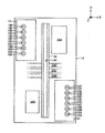
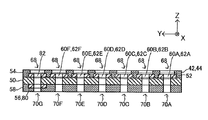
- FIG. 1 is a plan view of an electric device 10 according to the first embodiment.
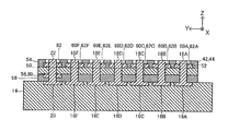
- FIG. 2 is a plan view of the base substrate 12 included in the electric device 10 according to the first embodiment.
- the X axis, the Y axis, and the Z axis are orthogonal to each other.
- symbols with black circles in white circles indicate axes in the direction from the paper surface toward the front
- symbols with x in white circles indicate An axis in a direction from the paper surface toward the back is represented.
- the electric device 10 of the present embodiment shown in FIG. 1 and the like is applied, for example, as an inverter for a motor of an electric vehicle.
- the inverter converts DC power supplied from a battery or a fuel cell into three-phase AC power and supplies the three-phase AC power to the motor, and converts three-phase regenerative power generated by the motor into DC power. It charges the battery.
- the electric device 10 includes a power module (strong electric component, not shown) including a power transistor such as an IGBT (Insulated Gate Bipolar Transistor) or a feedback diode, a smoothing capacitor (not shown) for smoothing a DC voltage, It includes three-phase busbars 34U, 34V, 34W (high-power components) and single-phase busbars (high-power components, not shown) connected to the module, a controller (not shown) for controlling a power module, a power supply device (not shown), These are mounted on the base substrate 12.
- a power module strong electric component, not shown
- a power transistor such as an IGBT (Insulated Gate Bipolar Transistor) or a feedback diode
- a smoothing capacitor (not shown) for smoothing a DC voltage
- It includes three-phase busbars 34U, 34V, 34W (high-power components) and single-phase busbars (high-power components, not shown) connected to the module, a controller (not shown) for controlling
- a first connector 14 (first electrical component) and a second connector 24 (second electrical component) constituting a circuit of the electrical device 10 are arranged on the base substrate 12 so as to be oblique to each other. I have.
- the first connector 14 and the second connector 24 are connected to a harness (not shown) and a rigid printed circuit board (not shown) that constitute the electric device 10.
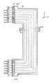
- External electrodes 16A-16F (connection pins 18A-18F extending in the Z-axis direction) are arranged on the upper surface of the first connector 14.
- External electrodes 26A-26F connection pins 28A-28F extending in the Z-axis direction
- the external electrodes 16A-16F and the external electrodes 26A-26F are electrically connected to each other by a flexible substrate 42 (wirings 60A-60F arranged on the flexible substrate 42).
- the number of external electrodes 16A-16F (connection pins 18A-18F) and the number of external electrodes 26A-26F (connection pins 28A-28F) are arbitrarily designed.
- a first structural component 36A (arbitrary component such as a device or a bracket) is arranged on the base substrate 12 so as to be adjacent to the first connector 14 in the X-axis direction, and a second structural component 36B is provided. Are arranged adjacent to each other in the X-axis direction with the second connector 24.
- the bracket 38 (fixing means) is disposed on the base substrate 12 for fixing, for example, the three-phase bus bars 34A, 34V, 34W (and / or single-phase bus bars) disposed on the base substrate 12.
- the bracket 38 has an elongated shape extending in the Y-axis direction and, for example, passes between the first connector 14 and the first structural component 36A and passes between the second connector 24 and the second structural component 36B. It is arranged to be.
- the bracket 38 has a fixing groove 40 (fixing means) formed along its longitudinal direction (Y-axis direction).
- the fixing groove 40 is formed so as to open at the upper surface of the bracket 38 and at both ends in the longitudinal direction, and the flexible substrate 42 is inserted therein.
- the upper surface of the first connector 14 and the upper surface of the second connector 24 are substantially flush with the upper surface of the base board 12, and the bracket 38 (three-sided) is provided between the first connector 14 and the second connector 24.
- the fixing groove 40 may be formed directly on the base substrate 12.
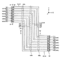
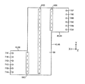
- FIG. 3 is a plan view of the flexible substrate 42 of the electric device 10 according to the first embodiment before deformation.
- FIG. 4 is a rear view of the flexible substrate 42 of the electric device 10 according to the first embodiment before deformation.
- FIG. 5 is a sectional view taken along line AA of FIG.
- FIG. 6 is a sectional view taken along line BB of FIG.
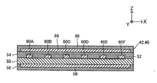
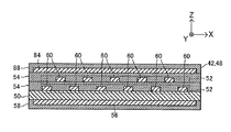
- the flexible substrate 42 cover layers 54, 58, and 88 is shown as transparent in the drawings.
- the flexible board 42 has a main surface formed in a crank shape following the arrangement of the first connector 14 and the second connector 24 on the base board 12.
- the flexible board 42 includes a first connection portion 44 connected to the first connector 14, a second connection portion 46 connected to the second connector 24, and the first connection portion 44 and the second connection portion 46. And an intermediate portion 48 that is disposed between them and inserted into the fixing groove 40.
- connection electrodes 62A to 62F (the number and arrangement form can be arbitrarily designed) connected to the external electrodes 16A to 16F (connection pins 18A to 18F) arranged on the first connector 14.
- the connection electrodes 64A-64F (the number and arrangement of the connection electrodes 64A-64F) connected to the external electrodes 26A-26F (connection pins 28A-28F) disposed on the second connector 24 are arbitrarily arranged. (Can be designed).
- the flexible substrate 42 also includes a wiring 60A connecting the connection electrode 62A and the connection electrode 64A, a wiring 60B connecting the connection electrode 62B and the connection electrode 64B, a wiring 60C connecting the connection electrode 62C and the connection electrode 64C, A wiring 60D connecting the connection electrode 62D and the connection electrode 64D, a wiring 60E connecting the connection electrode 62E and the connection electrode 64E, and a wiring 60F connecting the connection electrode 62F and the connection electrode 64F are arranged.
- the wires 60A to 60F pass through the intermediate portion 48 from the first connection portion 44 (connection electrodes 62A to 64F) while maintaining a state in which they are arranged in parallel at a predetermined interval, and the second connection portion 46 (connection).
- the electrodes are arranged so as to reach the electrodes 64A to 64F).
- the wirings 60A to 60F are used for transmitting and receiving a control signal to and from a controller and a power transistor, and for supplying a power supply voltage to a power supply device and a controller.
- the flexible substrate 42 has three folds (dashed lines) along the Y-axis direction.
- the fold is disposed at the boundary between the first connecting portion 44 and the intermediate portion 48, at the center of the intermediate portion 48 in the X-axis direction, at the boundary between the second connecting portion 46 and the intermediate portion 48, and is disposed at the intermediate portion. They are arranged so as to be parallel to the wirings 60A to 60F.
- the flexible substrate 42 is provided with deformation portions 66A-66C at positions overlapping the folds in plan view. The deformable portions 66A-66C are arranged so that the longitudinal direction thereof is along the fold of the flexible substrate 42.
- the deformable portions 66A to 66C deform the intermediate portion 48 of the flexible substrate 42 in the Z-axis direction (toward the base substrate 12) by plastically deforming the flexible substrate 42 along the fold before mounting the flexible substrate 42 on the base substrate 12. This is to add a bending habit for deforming into a shape. Thereby, the convex shape for the operator to insert the flexible substrate 42 (the intermediate portion 48) into the fixing groove 40 can be easily formed by the deformed portions 66A-66C, and the working efficiency can be improved.
- through holes 70A to 70F are formed at positions overlapping the connection electrodes 62A to 62F of the flexible substrate 42, and the through holes 70A to 70F are connected to the external electrodes 16A to 16F.
- the pins 18A-18F are inserted (FIGS. 10 and 11).
- through holes 71A-71F are formed at positions overlapping the connection electrodes 64A-64F of the flexible substrate 42, and the connection pins 28A-28F of the external electrodes 26A-26F are inserted into the through holes 71A-71F.
- the connection pins 18A to 18F and the connection pins 28A to 28F have a length equal to or greater than the thickness of the flexible board 42.
- An opening 68 communicating with the through holes 70A-70F is formed at a position of the cover layer 54 overlapping the connection electrodes 62A-62F, and the connection electrodes 62A-62F are exposed at the bottom surface of the opening 68.
- an opening 68 communicating with the through holes 71A-71F is formed in the cover layer 54 at a position overlapping the connection electrodes 64A-64F, and the connection electrodes 64A-64F are exposed at the bottom surface of the opening 68.
- the flexible substrate 42 is formed, for example, by using an adhesive (not shown) on one surface of the base layer 50 (the surface opposite to the surface on the base substrate 12 side, or the surface on the base substrate 12 side). ), A wiring layer 52 (first layer) for forming the wirings 60A to 60F, the connection electrodes 62A to 62F, and the connection electrodes 64A to 64F, and a cover layer 54 for protecting the wiring layer 52 are laminated. A metal layer 56 (second layer) forming the deformed portions 66A-66C and a cover layer 58 protecting the metal layer 56 are laminated on the surface (the surface on the base substrate 12 side or the surface opposite to the surface on the base substrate 12 side). Things.
- a material having excellent elasticity (flexibility) and insulating properties such as polyimide is applied.
- a material having high conductivity such as copper is applied to the wiring layer 52 and the metal layer 56, and a pattern is formed by etching.
- the metal layer 56 may be formed thicker than the wiring layer 52 to facilitate plastic deformation.
- FIG. 7 is a schematic diagram (part 1) illustrating an assembling process of the electric device 10 according to the first embodiment.
- FIG. 8 is a schematic diagram (part 2) illustrating an assembly process of the electric device 10 according to the first embodiment.
- FIG. 9 is a schematic diagram (part 3) illustrating an assembly process of the electric device 10 according to the first embodiment.
- FIG. 10 is a schematic diagram showing an arrangement relationship between the connection electrodes 62A-62F and the external electrodes 16A-16F in FIG. 8, and corresponds to a sectional view taken along the line BB of FIG.
- FIG. 11 is a schematic diagram showing an arrangement relationship between the connection electrodes 62A-62F and the external electrodes 16A-16F in FIG. 9, and corresponds to a sectional view taken along the line BB of FIG.
- the flexible substrate 42 is deformed so that the width of the intermediate portion 48 in the X-axis direction is reduced.
- the deformed portions 66A-66C are mainly deformed because stress is more concentrated in the deformed portions 66A-66C having the bending habit than in other portions of the flexible substrate 42.
- the width of the intermediate portion 48 in the X-axis direction is set to be substantially the same as or smaller than the width of the fixing groove 40. In this state, in the bent intermediate portion 48, a restoring force for returning to the shape shown in FIG. 7 is generated by the elastic force of the flexible substrate 42 (the base layer 50, the cover layers 54 and 58, and the metal layer 56). .
- the through holes 70A-70F penetrating the connection electrodes 62A-62F and the connection pins 18A-18F of the external electrodes 16A-16F are connected. They are arranged to face each other.
- through holes 71A-71F penetrating connection electrodes 64A-64F and connection pins 28A-28F of external electrodes 26A-26F are arranged so as to face each other.
- connection pins 18A-18F are inserted into the through holes 70A-70F, and the connection pins 18A-18F are brought into contact with the connection electrodes 62A-62F. Electrodes 16A-16F are electrically connected. Then, the first connection portion 44 is connected to the first connector 14 by soldering the connection electrodes 62A-62F and the connection pins 18A-18F.
- connection pins 28A-28F By inserting the connection pins 28A-28F into the through holes 71A-71F and bringing the connection pins 28A-28F into contact with the connection electrodes 64A-64F, the connection electrodes 64A-64F and the external electrodes 26A-26F are electrically connected. Is done. Then, the second connection portion 46 is connected to the second connector 24 by soldering the connection electrodes 62A-62F and the connection pins 18A-18F.
- FIG. 12 is a plan view of the electric device 10 of the comparative example.
- the first connector 14 disposed on the base substrate 12 has external electrodes 16A-16F
- the second connector 24 has external electrodes 26A-26F
- the external electrodes 16A-26F are connected to each other.
- a method of connecting the external electrodes 16A to 16F and the external electrodes 26A to 26F one by one with a coating wiring or the like can be considered, but the working efficiency is reduced.
- first connector 14 and the second connector 24 are designed so that the distance between them in the X-axis direction is reduced, it becomes difficult to connect the flexible board 42 having the shape shown in FIG.
- the restoring force generated by the deformation causes the flexible board 42 and the external electrodes 16 to be connected to each other. Is applied to the joint between the flexible substrate 42 and the external electrode 26, and the joint may be disconnected.
- a first structural component 36A is disposed adjacent to the first connector 14
- a second structural component 36B is disposed adjacent to the second connector 24, and the first structural component 36A and the second
- the height of the structural component 36B is higher than the heights of the first connector 14 and the second connector 24
- the flexible board 42 interferes with the first structural component 36A and the second structural component 36B.
- the interference can be avoided by deforming the flexible substrate 42, but the stress associated with the deformation is applied to the joint portion, and the risk of disconnection becomes significant. Further, with the vibration or acceleration / deceleration of the electric vehicle on which the electric device 10 is mounted, there is a possibility that a large stress is applied to the connection portion and the connection is broken.
- the intermediate portion 48 of the flexible board 42 is folded in a convex shape in the Z-axis direction (direction toward the base board 12), and the bracket 38 (the base board 12 May be formed) and the intermediate portion 48 having a convex shape is inserted.
- the bracket 38 the base board 12 May be formed
- the intermediate portion 48 having a convex shape is inserted.
- the occupied width (occupied area) of the intermediate portion 48 can be reduced. Therefore, interference of the intermediate portion 48 with other components on the base substrate 12 can be avoided, and the degree of freedom in designing the flexible substrate 42 can be improved.
- ⁇ ⁇ JP-A-11-68354 discloses a conventional configuration in which an end of a flexible wiring board is bent and held by holding ribs formed in a case.
- the fixing strength is not sufficient, and the ends are not supported by the vibration or acceleration / deceleration. There is a risk of leaving from
- the intermediate portion 48 inside the side of the flexible substrate 42 is bent into a convex shape and inserted into the fixing groove 40.
- the shape of the intermediate portion 48 can be stably maintained in the fixing groove 40.
- the intermediate portion 48 is turned up in the Z-axis direction by receiving a force (vibration or acceleration) from the outside, and becomes convex in the opposite direction to the base substrate 12 so that the intermediate portion 48 can be inserted into the fixing groove 40. There is no cancellation. Therefore, swing in the X-axis direction can be reduced.
- the contact position between the intermediate portion 48 and the fixing groove 40 is at two positions, one inner wall and the other inner wall of the fixing groove 40, and frictional forces in the Y-axis direction and the Z-axis direction are generated at these positions. Therefore, since there are two places where a frictional force is generated, the swing in the longitudinal direction (Y-axis direction) and the swing in the height direction (Z-axis direction) of the fixing groove 40 of the flexible substrate 42 are also more than those of the above-described conventional configuration. Can be suppressed.
- the flexible board 42 For example, in a case where 30 wires for passing a current of about 2 A (ampere) are arranged on the flexible board 42, 30 wires are arranged in the middle portion 48 of the flexible board 42 so as to be arranged in the X-axis direction. In order to avoid such a problem, the interval between the wirings needs to be about 1 mm. Therefore, in the comparative example shown in FIG. 12, the width of the intermediate portion 48 needs to be about 30 mm.
- the width of the intermediate portion 48 can be reduced to about 9 mm in plan view (as viewed from the Z-axis direction). Therefore, in the present embodiment, the width of the intermediate portion 48 can be reduced at a ratio of 9 mm / 30 mm as compared with the comparative example, and the degree of freedom in designing the flexible substrate 42 can be increased accordingly.
- the width of the bracket 38 in the X-axis direction is about 11 to 13 mm, and the width of the fixing groove 40 is 9 mm.
- the radius of curvature of the tip of the intermediate section 48 when the intermediate section 48 is inserted into the fixing groove 40 is designed to be about 2.5 mm. It is preferred to do so.
- the length of the convex shape of the intermediate portion 48 in the Z-axis direction is 10 mm or more. It is preferable that the depth of the groove 40 is also 10 mm or more.
- FIG. 13 is a schematic diagram of a first modified example of the electric device 10 of the first embodiment.
- FIG. 14 is a schematic diagram of a second modified example of the electric device 10 of the first embodiment.
- the first modification and the second modification are also configured to limit the swing of the flexible substrate 42 in the Z-axis direction also in the swing. In the first modification shown in FIG.
- two ear portions 72 are provided so as to sandwich the intermediate portion 48 in the intermediate portion 48, and the ear portions 72 are connected to the third structural component 36 ⁇ / b> C disposed on the base substrate 12,
- the swing of the intermediate portion 48 in the Z-axis direction (and the X-axis direction and the Y-axis direction) is limited by fixing the intermediate portion 48 to the structural component 36D with a rivet 74 or the like.
- a branch wiring 76 for branching the swing of the wirings 60 ⁇ / b> A to 60 ⁇ / b> F is formed, and the second wiring is formed. You may make it connectable to the structural component 36B etc.
- the lid 78 is attached to the base substrate 12, and the upper part of the lid 78 is in contact with the flexible substrate 42 to limit the swing of the flexible substrate 42 in the Z-axis direction. .
- the swing in the Z-axis direction can be sufficiently suppressed only by inserting the convex intermediate portion 48 into the fixing groove 40, the configurations of the first modification and the second modification are unnecessary.
- the electric device 10 includes a first connector 14, a second connector 24, a base board 12 on which the first connector 14 and the second connector 24 are mounted, and a first connector 14.
- the electric device 10 includes a flexible board 42 for connecting to the second connector 24.
- a fixing groove 40 is provided at a position between the first connector 14 and the second connector 24, and the flexible substrate 42 is bent at an intermediate portion 48 of the flexible substrate 42 and inserted into the fixing groove 40. As a result, it is fixed to the base substrate 12.
- the shape of the intermediate portion 48 can be stably maintained in the fixing groove 40.
- the intermediate portion 48 is turned up in the Z-axis direction by receiving a force (vibration or acceleration) from the outside, and becomes convex in the opposite direction to the base substrate 12 so that the intermediate portion 48 can be inserted into the fixing groove 40. It will not be released. Therefore, swing in the X-axis direction can be reduced.
- the contact position between the intermediate portion 48 and the fixing groove 40 is at two positions, one inner wall and the other inner wall of the fixing groove 40, and frictional forces in the Y-axis direction and the Z-axis direction are generated at these positions. Therefore, since there are two places where the frictional force is generated, the swinging in the longitudinal direction (Y-axis direction) and the height direction (Z-axis direction) of the fixing groove 40 of the flexible substrate 42 can be suppressed. .
- the intermediate portion 48 is bent into a convex shape and inserted into the fixing groove 40.
- the shape of the intermediate portion 48 into which the fixing groove 40 is inserted can be constructed with a simple configuration.
- high-voltage components (three-phase busbars 34A, 34V, 34W, single-phase busbars, etc.) are arranged at positions between the first connector 14 and the second connector 24 of the base board 12, and brackets are provided.
- Numeral 38 fixes the high-power component to the base substrate 12.
- the fixing groove 40 can be arranged on the bracket 38 for fixing the existing components of the electric device 10. This allows the flexible substrate 42 to be arranged without adding new components, thereby reducing costs.
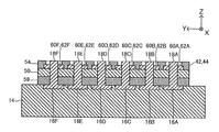
- the flexible substrate 42 includes a laminated structure of a wiring layer 52 and a metal layer 56
- the wiring layer 52 includes a wiring 60A- electrically connecting the first connector 14 and the second connector 24. 60F, the metal layer 56 is deformed following the bent shape of the intermediate portion 48.
- the stress is easily concentrated on the intermediate portion 48 by the bent shape (bending habit) of the intermediate portion 48, thereby facilitating the formation of the intermediate portion 48 at the time of mounting and improving the working efficiency.
- a plurality of wirings 60A to 60F are arranged on the flexible substrate 42, and the wirings 60A to 60F pass through the intermediate portion 48.
- FIG. 15 is a plan view of a flexible substrate 42 included in the electric device 10 according to the second embodiment before deformation.
- FIG. 16 is a rear view of the flexible substrate 42 of the electric device 10 according to the second embodiment before deformation.
- FIG. 17 is a sectional view taken along line AA of FIG.
- FIG. 18 is a sectional view taken along line BB of FIG.
- FIG. 19 is a plan view of the electric device 10 according to the second embodiment.
- FIG. 20 is a sectional view taken along line AA of FIG.
- the same components as those in the first embodiment are denoted by the same reference numerals, and the description thereof will be omitted unless necessary.
- the metal layer 56 is disposed so as to cover the wiring layer 52 in plan view (when viewed from the thickness direction of the flexible substrate 42), and the intermediate portion 48 is bent such that the metal layer 56 is on the outside. (See FIG. 7).
- the metal layer 56 includes the deformed portions 66A-66C as in the first embodiment, but the outer shape of the metal layer 56 accommodates most of the outer shape of the wirings 60A-60F in plan view. (FIG. 15). Further, the metal layer 56 is disposed on the surface of the base layer 50 on the base substrate 12 side, and the wiring layer 52 is disposed on the surface of the base layer 50 opposite to the surface on the base substrate 12 side (FIG. 17).
- a ground electrode 20 (connection pin 22) is arranged on the first connector 14 adjacent to the external electrode 16F, and is arranged on the second connector 24 adjacent to the external electrode 26F.
- the ground electrode 30 (connection pin 32) is arranged, and the metal layer 56 is electrically connected to the ground electrode 20 and the ground electrode 30.
- the metal layer 56 includes connection electrodes 80 extending from the wiring layer 52 (wirings 60A to 60F) in a plan view to positions adjacent to the connection electrode 62F and positions adjacent to the connection electrode 64F. (FIGS. 16 and 18).
- the wiring layer 52 is provided with a dummy electrode 82 spatially separated from the wirings 60A to 60F at positions overlapping the connection electrodes 80 in plan view (FIGS. 15 and 18).
- a through hole 70G penetrating the flexible substrate 42 (the connection electrode 80 and the dummy electrode 82) is formed at a position overlapping the connection electrode 80 and the dummy electrode 82 (FIG. 15). 16 and 18).
- a through hole 71 ⁇ / b> G that penetrates the flexible substrate 42 (the connection electrode 80 and the dummy electrode 82) is formed at a position overlapping the connection electrode 80 and the dummy electrode 82. (FIGS. 15, 16, and 18).
- connection pin 22 is inserted into the through hole 70G to make the connection pin 22 contact the connection electrode 80 and the dummy electrode 82
- connection pin 32 is inserted into the through hole 71G to connect the connection pin 32 to the connection electrode 80 and the dummy electrode 82.
- the metal layer 56 is electrically connected to the ground electrode 20 and the ground electrode 30 (FIGS. 19 and 20).
- the connection pins 22 and 32 are connected to the dummy electrodes 82 by soldering.
- the intermediate portion 48 of the flexible substrate 42 is bent so that the metal layer 56 is outside the convex shape and inserted into the fixing groove 40 (see FIG. 9), and is used for fixing the wirings 60A-60F.
- the portion inserted into the groove 40 is arranged so as to be covered with the metal layer 56 from the outside. Accordingly, noise traveling from the three-phase bus bars 34U, 34V, 34W disposed below the bracket 38 to the wirings 60A to 60F can be shielded. Note that the same effects as described above can be obtained even if the three-phase bus bars 34U, 34V, 34W fixed to the bracket 38 have any orientation on the base substrate 12.
- FIG. 21 is a plan view of a flexible substrate 42 included in the electric device 10 according to the third embodiment before deformation.
- FIG. 22 is a sectional view taken along line AA of FIG.
- FIG. 23 is a sectional view taken along line BB of FIG.
- FIG. 24 is a plan view of the electric device 10 according to the third embodiment.
- FIG. 25 is a sectional view taken along line AA of FIG.
- the flexible board 42 includes the wiring layer 52 including the wirings 60A to 60F for electrically connecting the first connector 14 and the second connector 24, and the flexible board 42 sandwiching the wiring layer 52.
- the laminated structure (FIG. 22) of a metal layer 56 (second layer) and a metal layer 84 (third layer) grounded when mounted on the base substrate 12 is included. 21 is arranged so as to cover the wiring layer 52 when viewed from the thickness direction (FIG. 21), and at least one of the metal layer 56 and the metal layer 84 is deformed following the bent shape of the intermediate portion 48 (FIG. 7). , FIG. 24).
- the flexible substrate 42 is similar to that of the second embodiment, but the metal layer 84 and the metal layer 84 covering the wiring layer 52 in plan view (when viewed from the thickness direction) are formed on the wiring layer 52. Is different in that a cover layer 88 for covering is added.
- the metal layer 84 is arranged such that its outer shape accommodates most of the outer shape of the wirings 60A to 60F inside.
- the metal layer 84 includes the connection electrode 86 extending to a position overlapping the connection electrode 80 of the metal layer 56 as described above in plan view (FIGS. 21, 23, and 24). Further, a through-hole 70G that penetrates the flexible substrate 42 is formed at a position where the connection electrode 80 and the connection electrode 86 overlap in plan view of the first connection portion 44 (FIGS. 21, 23, and 24). Similarly, a through-hole 71G penetrating the flexible substrate 42 is formed at a position where the connection electrode 80 and the connection electrode 86 overlap in a plan view of the second connection portion 46 (FIGS. 21, 23, and 24).
- connection pin 22 is inserted into the through hole 70 ⁇ / b> G of the first connection portion 44 so that the connection pin 22 contacts the connection electrode 80 and the connection electrode 86 (FIGS. 24 and 25), and the through hole of the second connection portion 46.
- connection pin 32 By inserting the connection pin 32 into the 71G and making the connection pin 32 contact the connection electrode 80 and the connection electrode 86, the metal layer 56 (connection electrode 80) and the metal layer 84 (connection electrode 86) are connected to the ground electrode 20 and the ground electrode. 30 and is electrically connected.
- the portions (intermediate portions 48) of the wirings 60A to 60F inserted into the fixing grooves 40 are covered with the metal layer 56 from the outside and covered with the metal layer 84 from the inside. It has become.
- the metal layer 56 can shield electric noise from the three-phase bus bars 34U, 34V, 34W disposed below the bracket 38 toward the wirings 60A to 60F.
- the electric device 10 of the present embodiment has a configuration in which the three-phase busbars 34U, 34V, 34W and other high-current components (such as single-phase busbars) pass over the flexible board 42.
- the metal layer 84 can shield electric noise from the high-voltage component toward the wirings 60A to 60F. Therefore, it is possible to improve the layout of the high-voltage components such as the three-phase bus bars 34U, 34V, and 34W in the electric device 10.
- the flexible substrate 42 has the same function and effect as described above even if the flexible substrate 42 is inserted into the fixing groove 40 with the metal layer 56 and the metal layer 84 reversed.
- FIG. 26 is a schematic view showing a modified example of the electric device 10 of the third embodiment.
- the wiring layer 52 (and the cover layer 54) constituting the wiring 60 has a two-layer structure.
- some of the wirings 60 arranged in a line at the boundary between the first connection portion 44 and the intermediate portion 48 are formed on a layer different from the remaining wirings 60 by using a laminated structure (not shown).
- the stacked structure is used again to form an array similar to the array of the wiring 60 in the first connecting portion 44 by using the stacked structure (not shown) again. You just have to return it.
- the increase in the width of the intermediate portion 48 can be suppressed even if the number of the wirings 60 increases, so that the degree of freedom in designing the flexible substrate 42 can be improved.
- the modified example can be applied to other embodiments.
- FIG. 27 is a schematic diagram of a flexible substrate 42 included in the electric device 10 according to the fourth embodiment before deformation.
- FIG. 28 is a schematic diagram when the flexible substrate 42 configuring the electric device 10 according to the fourth embodiment is bent.
- FIG. 29 is a plan view of the electric device 10 according to the fourth embodiment.
- the flexible substrate 42 of the present embodiment is similar to the third embodiment, but the intermediate portion 48 has a wavy shape that oscillates in the width direction (X-axis direction) of the fixing groove 40, and has an antinode of the wavy shape. At the position, it is fixed to the fixing groove 40 by being pressed against the inner wall of the fixing groove 40.
- the intermediate portion 48 of the flexible substrate 42 is formed so as to have a wave-like amplitude in the X-axis direction by being compressed in the Y-axis direction.
- the work efficiency is better when the wavy shape is formed in a state where the intermediate portion 48 is arranged in the fixing groove 40.
- the first connector 14 is connected to the first connection portion 44, and the second connector 24 is connected to the second connection portion 46, whereby the wave shape of the intermediate portion 48 is maintained (FIG. 29).
- the cover layer 58 (and the metal layer 56) becomes the upper surface.
- the swing of the flexible substrate 42 (the intermediate portion 48) in the X-axis direction is suppressed by the intermediate portion 48 applying a force to the inner walls on both sides of the fixing groove 40. Further, the swing in the Y-axis direction and the swing in the Z-axis direction are suppressed by the frictional force between the intermediate portion 48 and the inner walls on both sides of the fixing groove 40.
- the wiring layer 52 is sandwiched between the metal layer 56 and the metal layer 84 in the X-axis direction (see FIG. 22). Therefore, even if strong electric components such as the three-phase bus bars 34U, 34V, 34W (not shown in FIG. 29) are arranged in the area indicated by the broken line in FIG. 29 (the area sandwiching the bracket 38 in the X-axis direction), the metal layer 56 and the The metal layer 84 can shield electric noise from the high-voltage component toward the wiring layer 52.
- the fourth embodiment can be applied to the first to third embodiments. That is, in the first to third embodiments, the intermediate portion 48 of the flexible board 42 may be corrugated as in the fourth embodiment and fixed to the fixing groove 40 without bending the intermediate portion 48 into a convex shape. In a state where the portion 48 is formed in a convex shape, it may be further fixed in the fixing groove 40 in a wavy shape as in the fourth embodiment.
Landscapes
- Engineering & Computer Science (AREA)
- Microelectronics & Electronic Packaging (AREA)
- Structure Of Printed Boards (AREA)
Abstract
第1のコネクタと、第2のコネクタと、第1のコネクタと第2のコネクタが搭載されたべース基板と、第1のコネクタと第2のコネクタとを接続するフレキシブル基板とを有する電気装置である。そして、第1のコネクタと第2のコネクタとの間となる位置には固定用溝が設けられ、フレキシブル基板は、フレキシブル基板の中間部において折り曲げられ固定用溝に差し込まれることでベース基板に固定される。
Description
本発明は、電気装置に関する。
特開平11−68354公報は、フレキシブル配線板(フレキシブル基板)の端部を折り曲げてケースに形成された保持リブに保持させる構成を開示している。
しかし、上記構成では、フレキシブル基板の端部のみが固定される態様となるので、フレキシブル基板が大きくなるとその固定強度が十分でなくなる。
そこで、本発明は、フレキシブル基板の固定強度を高めた電気装置を提供することを目的とする。
本発明の一態様は、第1の電気部品と、第2の電気部品と、第1の電気部品と第2の電気部品が搭載されたベース基板と、第1の電気部品と第2の電気部品とを接続するフレキシブル基板とを有する電気装置において、第1の電気部品と第2の電気部品との間となる位置には固定手段が設けられ、フレキシブル基板は、フレキシブル基板の中間部において折り曲げられ固定手段に差し込まれることでベース基板に固定される。
以下、図面を参照しながら、本発明の実施形態について説明する。
[第1実施形態]
図1は、第1実施形態の電気装置10の平面図である。図2は、第1実施形態の電気装置10を構成するベース基板12の平面図である。なお明細書及び図面において、X軸、Y軸、Z軸は互いに直交するものとする。また図中の座標軸(X軸、Y軸、Z軸)において、白丸印の中に黒丸印がある記号は紙面から手前に向かう方向の軸を表し、白丸印の中に×印がある記号は紙面から奥に向かう方向の軸を表すものとする。
図1は、第1実施形態の電気装置10の平面図である。図2は、第1実施形態の電気装置10を構成するベース基板12の平面図である。なお明細書及び図面において、X軸、Y軸、Z軸は互いに直交するものとする。また図中の座標軸(X軸、Y軸、Z軸)において、白丸印の中に黒丸印がある記号は紙面から手前に向かう方向の軸を表し、白丸印の中に×印がある記号は紙面から奥に向かう方向の軸を表すものとする。
図1等に示す本実施形態の電気装置10は、例えば、電動車両のモータ用のインバータとして適用される。インバータは、バッテリや燃料電池から供給された直流の電力を三相交流の電力に変換してモータに供給するものであり、またモータで発生した三相の回生電力を直流の電力に変換してバッテリに充電するものである。
本実施形態の電気装置10は、IGBT(Insulated Gate Bipolar Transistor)等のパワートランジスタや帰還ダイオードを備えたパワーモジュール(強電部品、不図示)、直流電圧を平滑化する平滑コンデンサ(不図示)、パワーモジュールに接続された三相バスバ34U,34V,34W(強電部品)及び単相バスバ(強電部品、不図示)、パワーモジュールを制御するコントローラ(不図示)、電源装置(不図示)等を備え、これらがベース基板12に取り付けられている。
ベース基板12には、電気装置10の回路を構成する第1のコネクタ14(第1の電気部品)及び第2のコネクタ24(第2の電気部品)が互いに斜向かいとなるように配置されている。第1のコネクタ14及び第2のコネクタ24は、電気装置10を構成するハーネス(不図示)やリジッドプリント基板(不図示)に接続されている。第1のコネクタ14の上面には外部電極16A−16F(Z軸方向に延びる接続ピン18A−18F)が配置されている。第2のコネクタ24の上面には外部電極26A−26F(Z軸方向に延びる接続ピン28A−28F)が配置されている。外部電極16A−16Fと外部電極26A−26Fとがフレキシブル基板42(フレキシブル基板42に配置された配線60A−60F)により互いに電気的に接続される。なお、外部電極16A−16F(接続ピン18A−18F)及び外部電極26A−26F(接続ピン28A−28F)の個数は任意に設計される。
その他、ベース基板12には、第1の構造部品36A(デバイス、ブラケット等の任意の構成要素)が第1のコネクタ14とX軸方向で互いに隣接するように配置され、第2の構造部品36Bが第2のコネクタ24とX軸方向で互いに隣接するように配置されている。
ブラケット38(固定手段)は、例えば、ベース基板12上に配置された三相バスバ34A,34V,34W(及び/若しくは、単相バスバ)を固定するためにベース基板12に配置されるものである。ブラケット38は、Y軸方向に延びる細長形状を有し、例えば、第1のコネクタ14と第1の構造部品36Aとの間、第2のコネクタ24と第2の構造部品36Bとの間を通過するように配置されている。
ブラケット38には、その長手方向(Y軸方向)に沿って固定用溝40(固定手段)が形成されている。固定用溝40は、ブラケット38の上面及び長手方向の両端において開口するように形成されており、フレキシブル基板42が差し込まれる。
なお、第1のコネクタ14及び第2のコネクタ24の上面がベース基板12の上面とほぼ同一平面を形成する場合であって第1のコネクタ14と第2のコネクタ24の間にブラケット38(三相バスバ34U,34V,34W)が配置されていない場合、固定用溝40は、ベース基板12に直接形成してもよい。
図3は、第1実施形態の電気装置10を構成するフレキシブル基板42の変形前の平面図である。図4は、第1実施形態の電気装置10を構成するフレキシブル基板42の変形前の裏面図である。図5は、図3のA−A線断面図である。図6は、図3のB−B線断面図である。なお、フレキシブル基板42の内部構造の視認を容易にするため、図面においてフレキシブル基板42(カバー層54,58,88)は透明なものとして図示している。
図3に示すように、フレキシブル基板42は、その主面がベース基板12上の第1のコネクタ14及び第2のコネクタ24の配置に倣ってクランク形に形成されたものである。
フレキシブル基板42は、第1のコネクタ14に接続する第1の接続部44と第2のコネクタ24に接続される第2の接続部46と、第1の接続部44と第2の接続部46の間に配置され固定用溝40に差し込まれる中間部48とを有する。
第1の接続部44には、第1のコネクタ14に配置された外部電極16A−16F(接続ピン18A−18F)に接続する接続電極62A−62F(個数及び配置形態は任意に設計可能)が配置されており、第2の接続部46には第2のコネクタ24に配置された外部電極26A−26F(接続ピン28A−28F)に接続する接続電極64A−64F(個数及び配置形態は任意に設計可能)が配置されている。
また、フレキシブル基板42には、接続電極62Aと接続電極64Aとを接続する配線60A、接続電極62Bと接続電極64Bとを接続する配線60B、接続電極62Cと接続電極64Cとを接続する配線60C、接続電極62Dと接続電極64Dとを接続する配線60D、接続電極62Eと接続電極64Eとを接続する配線60E、接続電極62Fと接続電極64Fとを接続する配線60Fが配置されている。配線60A−60Fは所定の間隔を空けて並列に並んだ状態を維持しつつ第1の接続部44(接続電極62A−64F)から、中間部48を通過し、第2の接続部46(接続電極64A−64F)に到達するように配置されている。なお、配線60A−60Fは、コントローラやパワートランジスタに対する制御信号の送受信、電源装置やコントローラへの電源電圧の供給に用いられる。
図3、図4に示すように、フレキシブル基板42には、Y軸方向に沿って3箇所の折り目(一点鎖線)が形成されている。折り目は第1の接続部44と中間部48との境界、中間部48のX軸方向の中央部、第2の接続部46と中間部48との境界に配置され、中間部に配置された配線60A−60Fと平行となるように配置されている。また、フレキシブル基板42には、平面視で当該折り目と重なる位置に変形部66A−66Cを備えている。変形部66A−66Cは、その長手方向がフレキシブル基板42の折り目に沿うように配置されている。また、変形部66A−66Cは、フレキシブル基板42をベース基板12に実装する前に折り目に沿って塑性変形させることで、フレキシブル基板42の中間部48をZ軸方向(ベース基板12側)に凸形状に変形させるための曲げ癖を付けるものである。これにより、作業者がフレキシブル基板42(中間部48)を固定用溝40に差し込むための凸形状を変形部66A−66Cにより容易に形成して作業効率を向上させることができる。
図3、図4に示すように、フレキシブル基板42の接続電極62A−62Fと重なる位置には、貫通孔70A−70Fが形成されており、貫通孔70A−70Fには外部電極16A−16Fの接続ピン18A−18Fが挿通する(図10、図11)。同様に、フレキシブル基板42の接続電極64A−64Fと重なる位置には、貫通孔71A−71Fが形成されており、貫通孔71A−71Fには外部電極26A−26Fの接続ピン28A−28Fが挿通する。接続ピン18A−18F及び接続ピン28A−28Fは、フレキシブル基板42の厚み以上の長さを有する。
カバー層54の接続電極62A−62Fに重なる位置には貫通孔70A−70Fに連通する開口部68が形成され、開口部68の底面において接続電極62A−62Fが露出する。同様に、カバー層54の接続電極64A−64Fに重なる位置には貫通孔71A−71Fに連通する開口部68が形成され、開口部68の底面において接続電極64A−64Fが露出する。
図5、6に示すように、フレキシブル基板42は、例えば、接着剤(不図示)を用いてベース層50の一方の面(ベース基板12側の面の反対面、又はベース基板12側の面)に配線60A−60F、接続電極62A−62F、及び接続電極64A−64Fを形成する配線層52(第1層)、配線層52を保護するカバー層54を積層し、ベース層50の他方の面(ベース基板12側の面、又はベース基板12側の面の反対面)に変形部66A−66Cを形成する金属層56(第2層)及び金属層56を保護するカバー層58を積層したものである。ベース層50及びカバー層54,58はポリイミド等の弾力性(可撓性)と絶縁性の優れた材料が適用される。また、配線層52及び金属層56は銅などの導電性の高い材料が適用され、エッチングによりパターンが形成される。金属層56は、塑性変形を容易にするため配線層52よりも厚く形成してもよい。
図7は、第1実施形態の電気装置10の組み付け工程を示す模式図(その1)である。図8は、第1実施形態の電気装置10の組み付け工程を示す模式図(その2)である。図9は、第1実施形態の電気装置10の組み付け工程を示す模式図(その3)である。図10は、図8における接続電極62A−62Fと外部電極16A−16Fとの配置関係を示す模式図であって図3のB−B線断面図に対応するものである。図11は、図9における接続電極62A−62Fと外部電極16A−16Fとの配置関係を示す模式図であって図3のB−B線断面図に対応するものである。
次に、フレキシブル基板42をベース基板12に組み付ける工程について説明する。
図7に示すように、図3に示すように形成されたフレキシブル基板42において、変形部66A、変形部66B、変形部66Cに重なる位置においてプレス機等を用いて折り目を形成する。このとき、中間部48において金属層56側が山折りになるように折り目を形成する。これにより、フレキシブル基板42中の変形部66A−66Cは塑性変形し、フレキシブル基板42には凸形状の曲げ癖が形成される。ただし、当該フレキシブル基板42に何ら負荷を与えない場合、両端にある二つの折り目(変形部66A、変形部66C)の間隔は固定用溝40の幅よりも広くなる。
図8に示すように、中間部48のX軸方向の幅が狭くなるようにフレキシブル基板42を変形させる。このとき、曲げ癖を備えた変形部66A−66Cはフレキシブル基板42の他の部分よりも応力が集中するので変形部66A−66Cが主として変形する。さらに、フレキシブル基板42について、中間部48のX軸方向の幅を固定用溝40の幅と同程度若しくは当該幅よりも狭くなるようにする。この状態において、折り曲げられた中間部48では、フレキシブル基板42(ベース層50、カバー層54,58、金属層56)の弾性力により図7に示す形状に戻ろうとする復元力が発生している。
また、このとき、図10(図9、図11の直前の状態)に示すように、接続電極62A−62Fを貫通する貫通孔70A−70Fと外部電極16A−16Fの接続ピン18A−18Fとが互いに対向するように配置される。同様に、接続電極64A−64Fを貫通する貫通孔71A−71Fと外部電極26A−26Fの接続ピン28A−28Fとが互いに対向するように配置される。
図9に示すように、フレキシブル基板42の中間部48を固定用溝40に差し込む。すると中間部48は、自身が持つ復元力により固定用溝40の互いに対向する2つの内壁に当接し、固定用溝40の幅を広げる方向の力を2つの内壁に付与することになる。これにより、ベース基板12に対するフレキシブル基板42のX軸方向(幅方向)の揺動(ズレ)を抑制することができる。またフレキシブル基板42と固定用溝40との間の摩擦力によりフレキシブル基板42のY軸方向(長手方向)の揺動及びZ軸方向(高さ方向)の揺動も抑制することができる。
また、このとき、図11に示すように貫通孔70A−70Fに接続ピン18A−18Fを挿通して接続ピン18A−18Fを接続電極62A−62Fに接触させることで、接続電極62A−62Fと外部電極16A−16Fが電気的に接続される。そして、接続電極62A−62Fと接続ピン18A−18Fとを半田付けすることにより、第1の接続部44が第1のコネクタ14に接続される。
同様に貫通孔71A−71Fに接続ピン28A−28Fを挿通して接続ピン28A−28Fを接続電極64A−64Fに接触させることで、接続電極64A−64Fと外部電極26A−26Fが電気的に接続される。そして、接続電極62A−62Fと接続ピン18A−18Fとを半田付けすることにより、第2の接続部46が第2のコネクタ24に接続される。
[第1実施形態と比較例との対比]
図12は、比較例の電気装置10の平面図である。図12に示すように、例えば、ベース基板12に配置された第1のコネクタ14には外部電極16A−16Fがあり、第2のコネクタ24には外部電極26A−26Fがあり、外部電極16A−16Fと外部電極26A−26Fを互いに接続する場合を考える。このとき、例えば外部電極16A−16Fと外部電極26A−26Fを被覆配線等で一つずつ接続していく方法も考えられるが作業効率が低下する。そこで、外部電極16A−16F、及び外部電極26A−26Fの配置形態及び接続形態に倣って配線60A−60Fを配置したフレキシブル基板42により、両者を電気的に接続する構成が考えられる。しかし、配線60A−60Fに流す電流が比較的大きい場合には、配線60A−60Fの配置間隔を広く設計する必要がある。
図12は、比較例の電気装置10の平面図である。図12に示すように、例えば、ベース基板12に配置された第1のコネクタ14には外部電極16A−16Fがあり、第2のコネクタ24には外部電極26A−26Fがあり、外部電極16A−16Fと外部電極26A−26Fを互いに接続する場合を考える。このとき、例えば外部電極16A−16Fと外部電極26A−26Fを被覆配線等で一つずつ接続していく方法も考えられるが作業効率が低下する。そこで、外部電極16A−16F、及び外部電極26A−26Fの配置形態及び接続形態に倣って配線60A−60Fを配置したフレキシブル基板42により、両者を電気的に接続する構成が考えられる。しかし、配線60A−60Fに流す電流が比較的大きい場合には、配線60A−60Fの配置間隔を広く設計する必要がある。
一方、第1のコネクタ14と第2のコネクタ24とのX軸方向の間隔が狭くなるように設計されている場合、図12に示す形状のフレキシブル基板42の接続が困難になる。もちろん、フレキシブル基板42を変形させることによりフレキシブル基板42を第1のコネクタ14及び第2のコネクタ24に接続することは可能であるが、当該変形によって生じる復元力がフレキシブル基板42と外部電極16との接合部分、フレキシブル基板42と外部電極26との接合部分に付与され当該接合部分が断線する虞がある。
また、第1の構造部品36Aが第1のコネクタ14に隣接して配置され、第2の構造部品36Bが第2のコネクタ24に隣接して配置され、且つ第1の構造部品36A及び第2の構造部品36Bの高さが第1のコネクタ14及び第2のコネクタ24の高さよりも高い場合を考える。この場合、第1のコネクタ14及び第2のコネクタ24にフレキシブル基板42を接続しようとするとフレキシブル基板42が第1の構造部品36A及び第2の構造部品36Bに干渉する。この場合も、フレキシブル基板42を変形させて当該干渉を回避することも可能であるが、当該変形に伴う応力が前記の接合部分に付与されて断線する虞が顕著となる。さらに、電気装置10が搭載された電動車両の振動や加減速に伴い、当該接合部分に大きな応力が付与され断線する虞もある。
これに対して、本実施形態では、図1に示すように、フレキシブル基板42の中間部48をZ軸方向(ベース基板12に向かう方向)に向けて凸形状に折り畳み、ブラケット38(ベース基板12でもよい)に固定用溝40を形成して凸形状となった中間部48を差し込む構成としている。これにより、中間部48の幅が配線60A−60Fの配置により広くなったとしても中間部48は凸形状に折り曲げられて固定用溝40に差し込まれるため、ベース基板12への実装後において平面視したときの中間部48の占有幅(占有面積)を小さくすることができる。よって、中間部48のベース基板12上の他の構成要素との干渉を回避でき、フレキシブル基板42の設計の自由度を向上させることができる。
前記した特開平11−68354公報では、フレキシブル配線板の端部を折り曲げてケースに形成された保持リブに保持させる従来構成を開示している。しかし、上記のようにフレキシブル配線板の端部のみが固定される態様となるので、フレキシブル配線板が大きくなるとその固定強度が十分でなくなり、外部からの振動又は加減速により当該端部が保持リブから離脱する虞がある。
これに対して、本実施形態では、フレキシブル基板42の辺よりも内側となる中間部48を凸形状に折り曲げて固定用溝40に差し込む構成となっている。当該構成により、中間部48は固定用溝40内においてその形状を安定的に維持することができる。例えば、中間部48が外部から力(振動、加速度)を受けてZ軸方向にめくれ上がり、ベース基板12に対して反対方向に凸形状になって中間部48の固定用溝40への差し込みが解除されるようなことはない。したがって、X軸方向の揺動を低減することができる。
また、中間部48と固定用溝40との接触位置は固定用溝40の一方の内壁と他方の内壁の2箇所となり、当該位置においてY軸方向及びZ軸方向の摩擦力も発生する。よって、摩擦力を発生させる箇所が2箇所あるためフレキシブル基板42の固定用溝40の長手方向(Y軸方向)の揺動及び高さ方向(Z軸方向)の揺動も上記従来構成よりも抑制することができる。
例えば、フレキシブル基板42に2A(アンペア)程度の電流を流す配線を30本配置する場合、フレキシブル基板42の中間部48には30本の配線がX軸方向に並ぶように配置されるが、短絡等を回避するため配線の並ぶ間隔は1mm程度必要となる。よって、図12に示す比較例において、中間部48の幅は30mm程度必要となる。
一方、本実施形態では、フレキシブル基板42の厚みを50μm程度に設計した場合、中間部48の幅を平面視で(Z軸方向から見て)9mm程度まで低下させることができる。よって、本実施形態では、中間部48の幅を比較例と比較して9mm/30mmの割合で低下させることができ、その分、フレキシブル基板42の設計の自由度を高めることができる。
ここで、ブラケット38のX軸方向の幅は11−13mm程度、固定用溝40の幅は9mmとしている。また、上記のようにフレキシブル基板42の厚みを50μm程度に設計した場合、中間部48を固定用溝40に差し込んだときの中間部48の先端の曲率半径は2.5mm程度となるように設計することが好適である。また、中間部48によりフレキシブル基板42を固定用溝40に固定するためには、中間部48の凸形状のZ軸方向の長さが10mm以上あることが好適であり、これに対応して固定用溝40の深さも10mm以上あることが好適である。
[第1実施形態の変形例]
図13は、第1実施形態の電気装置10の第1変形例の模式図である。図14は、第1実施形態の電気装置10の第2変形例の模式図である。第1変形例及び第2変形例はい揺動もフレキシブル基板42のZ軸方向の揺動を制限する構成となっている。図13に示す第1変形例では、中間部48において中間部48を挟むように2つの耳部72を設け、耳部72をベース基板12に配置された第3の構造部品36C、第4の構造部品36Dにリベット74等で固定することで中間部48のZ軸方向(及びX軸方向とY軸方向)の揺動を制限している。
図13は、第1実施形態の電気装置10の第1変形例の模式図である。図14は、第1実施形態の電気装置10の第2変形例の模式図である。第1変形例及び第2変形例はい揺動もフレキシブル基板42のZ軸方向の揺動を制限する構成となっている。図13に示す第1変形例では、中間部48において中間部48を挟むように2つの耳部72を設け、耳部72をベース基板12に配置された第3の構造部品36C、第4の構造部品36Dにリベット74等で固定することで中間部48のZ軸方向(及びX軸方向とY軸方向)の揺動を制限している。
なお、図13に示すように、フレキシブル基板42において更なる積層構造(不図示)を構築することにより、配線60A−60Fのうちのい揺動かを分岐させる分岐配線76を形成して第2の構造部品36B等に接続できるようにしてもよい。
図14に示す第2変形例では、ベース基板12に蓋部78を取り付けるとともに蓋部78の上部がフレキシブル基板42に当接するようにしてフレキシブル基板42のZ軸方向の揺動を制限している。ただし、固定用溝40に凸形状の中間部48を差し込むだけでZ軸方向の揺動を十分に抑制できるのであれば、第1変形例及び第2変形例の構成は不要である。
[第1実施形態の効果]
第1実施形態の電気装置10は、第1のコネクタ14と、第2のコネクタ24と、第1のコネクタ14と第2のコネクタ24が搭載されたベース基板12と、第1のコネクタ14と第2のコネクタ24とを接続するフレキシブル基板42とを有する電気装置10である。そして、第1のコネクタ14と第2のコネクタ24との間となる位置には固定用溝40が設けられ、フレキシブル基板42は、フレキシブル基板42の中間部48において折り曲げられ固定用溝40に差し込まれることでベース基板12に固定される。
第1実施形態の電気装置10は、第1のコネクタ14と、第2のコネクタ24と、第1のコネクタ14と第2のコネクタ24が搭載されたベース基板12と、第1のコネクタ14と第2のコネクタ24とを接続するフレキシブル基板42とを有する電気装置10である。そして、第1のコネクタ14と第2のコネクタ24との間となる位置には固定用溝40が設けられ、フレキシブル基板42は、フレキシブル基板42の中間部48において折り曲げられ固定用溝40に差し込まれることでベース基板12に固定される。
上記構成により、中間部48は固定用溝40内においてその形状を安定的に維持することができる。例えば、中間部48が外部から力(振動、加速度)を受けてZ軸方向にめくれ上がり、ベース基板12に対して反対方向に凸形状になって中間部48の固定用溝40への差し込みが解除されることはない。したがって、X軸方向の揺動を低減することができる。
また、中間部48と固定用溝40との接触位置は固定用溝40の一方の内壁と他方の内壁の2箇所となり、当該位置においてY軸方向及びZ軸方向の摩擦力も発生する。よって、摩擦力を発生させる箇所が2箇所あるためフレキシブル基板42の固定用溝40の長手方向(Y軸方向)の揺動及び高さ方向(Z軸方向)の揺動を抑制することができる。
本実施形態において、中間部48は、凸形状に折り曲げられて固定用溝40に差し込まれている。これにより、簡易な構成で固定用溝40の差し込む中間部48の形状を構築することができる。
本実施形態において、ベース基板12の第1のコネクタ14と第2のコネクタ24との間となる位置には強電部品(三相バスバ34A,34V,34W、単相バスバ等)が配置され、ブラケット38は、強電部品をベース基板12に固定する。
上記構成により、電気装置10における既存の構成要素を固定するブラケット38に固定用溝40を配置することができる。これにより、新たな構成要素を追加することなく、フレキシブル基板42を配置できるので、コストを抑制することができる。
本実施形態において、フレキシブル基板42は、配線層52と金属層56との積層構造を含み、配線層52は、第1のコネクタ14と第2のコネクタ24とを電気的に接続する配線60A−60Fを含み、金属層56は、中間部48の折り曲げ形状に倣って変形している。
上記構成により、中間部48の折り曲げ形状(曲げ癖)により中間部48に応力を集中しやすくすることで実装時の中間部48の形成を容易にし、作業効率を向上させることができる。
本実施形態において、フレキシブル基板42には複数の配線60A−60Fが配置され、配線60A−60Fは中間部48を通過している。上記構成により、中間部48の幅が配線60A−60Fの配置により広くなったとしても中間部48は折り曲げられて固定用溝40に差し込まれるため、ベース基板12への実装後において平面視したときの中間部48の占有幅(占有面積)を小さくすることができる。よって、中間部48のベース基板12上の他の構成要素との干渉を回避でき、フレキシブル基板42の設計の自由度を向上させることができる。
[第2実施形態]
図15は、第2実施形態の電気装置10を構成するフレキシブル基板42の変形前の平面図である。図16は、第2実施形態の電気装置10を構成するフレキシブル基板42の変形前の裏面図である。図17は、図15のA−A線断面図である。図18は、図16のB−B線断面図である。図19は、第2実施形態の電気装置10の平面図である。図20は、図19のA−A線断面図である。なお、以後の説明において、第1実施形態と共通の構成要素については同一番号を付し、必要な場合を除いてその説明を省略する。
図15は、第2実施形態の電気装置10を構成するフレキシブル基板42の変形前の平面図である。図16は、第2実施形態の電気装置10を構成するフレキシブル基板42の変形前の裏面図である。図17は、図15のA−A線断面図である。図18は、図16のB−B線断面図である。図19は、第2実施形態の電気装置10の平面図である。図20は、図19のA−A線断面図である。なお、以後の説明において、第1実施形態と共通の構成要素については同一番号を付し、必要な場合を除いてその説明を省略する。
第2実施形態において、金属層56は、平面視で(フレキシブル基板42の厚み方向から見て)配線層52を覆うように配置され、中間部48は、金属層56が外側となるように折り曲げられている(図7参照)。
すなわち、金属層56は第1実施形態と同様に変形部66A−66Cを包含するものであるが、平面視してその外形が配線60A−60Fの外形のほとんどの部分を内側に収容するように配置されている(図15)。また、金属層56がベース層50のベース基板12側の面に配置され、配線層52がベース層50のベース基板12側の面の反対面に配置されている(図17)。
図19、図20に示すように、第1のコネクタ14には外部電極16Fに隣接して接地電極20(接続ピン22)が配置され、第2のコネクタ24には外部電極26Fに隣接して接地電極30(接続ピン32)が配置され、金属層56は接地電極20及び接地電極30に電気的に接続されるようになっている。
金属層56は、平面視で配線層52(配線60A−60F)からはみ出た位置であって接続電極62Fに隣接する位置、及び接続電極64Fに隣接する位置にまでそれぞれ延出した接続電極80を備えている(図16、図18)。一方、配線層52は、平面視で接続電極80と重なる位置には配線60A−60Fとは空間的に分離したダミー電極82を備えている(図15、図18)。
フレキシブル基板42の第1の接続部44において、接続電極80及びダミー電極82と重なる位置にはフレキシブル基板42(接続電極80、ダミー電極82)を貫通する貫通孔70Gが形成されている(図15、図16、図18)。同様に、フレキシブル基板42の第2の接続部46において、接続電極80及びダミー電極82と重なる位置にはフレキシブル基板42(接続電極80、ダミー電極82)を貫通する貫通孔71Gが形成されている(図15、図16、図18)。
そして、貫通孔70Gに接続ピン22を挿通して接続ピン22を接続電極80及びダミー電極82に接触させ、貫通孔71Gに接続ピン32を挿通して接続ピン32を接続電極80及びダミー電極82に接触することで、金属層56は接地電極20及び接地電極30に電気的に接続される(図19、図20)。また、半田付けにより接続ピン22,32はダミー電極82にそれぞれ接続される。
図19に示すように、フレキシブル基板42の中間部48は金属層56が凸形状の外側となるように折り曲げられて固定用溝40に差し込まれ(図9参照)、配線60A−60Fの固定用溝40に差し込まれた部分は外側から金属層56に覆われた配置となっている。これにより、ブラケット38の下に配置された三相バスバ34U,34V,34Wから配線60A−60Fに向かうノイズを遮蔽することができる。なお、ブラケット38に固定された三相バスバ34U,34V,34Wが、ベース基板12上で任意の向きであっても上記同様の効果を奏する。
[第3実施形態]
図21は、第3実施形態の電気装置10を構成するフレキシブル基板42の変形前の平面図である。図22は、図21のA−A線断面図である。図23は、図21のB−B線断面図である。図24は、第3実施形態の電気装置10の平面図である。図25は、図24のA−A線断面図である。
図21は、第3実施形態の電気装置10を構成するフレキシブル基板42の変形前の平面図である。図22は、図21のA−A線断面図である。図23は、図21のB−B線断面図である。図24は、第3実施形態の電気装置10の平面図である。図25は、図24のA−A線断面図である。
第3実施形態において、フレキシブル基板42は、第1のコネクタ14と第2のコネクタ24とを電気的に接続する配線60A−60Fを含む配線層52と、配線層52を挟み込むとともにフレキシブル基板42をベース基板12に実装すると接地される金属層56(第2層)及び金属層84(第3層)と、の積層構造(図22)を含み、金属層56及び金属層84は、フレキシブル基板42の厚み方向から見て配線層52を覆うように配置され(図21)、金属層56及び金属層84のうちの少なくとも一方は、中間部48の折り曲げ形状に倣って変形している(図7、図24参照)。
すなわち、本実施形態において、フレキシブル基板42は第2実施形態のものと類似するが、配線層52の上に平面視で(厚み方向から見て)配線層52を覆う金属層84及び金属層84をカバーするカバー層88が追加されている点で相違する。ここで、金属層84は、その外形が配線60A−60Fの外形のほとんどの部分を内側に収容するように配置されている。
金属層84は平面視で前記のように金属層56の接続電極80と重なる位置に延出した接続電極86を備えている(図21、図23、図24)。また、第1の接続部44の平面視で接続電極80と接続電極86が重なる位置においてフレキシブル基板42を貫通する貫通孔70Gが形成されている(図21、図23、図24)。同様に、第2の接続部46の平面視で接続電極80と接続電極86が重なる位置においてフレキシブル基板42を貫通する貫通孔71Gが形成されている(図21、図23、図24)。
第1の接続部44の貫通孔70Gに接続ピン22を挿通して接続ピン22を接続電極80及び接続電極86に接触させ(図24、図25)、また第2の接続部46の貫通孔71Gに接続ピン32を挿通して接続ピン32を接続電極80及び接続電極86に接触することで、金属層56(接続電極80)及び金属層84(接続電極86)が接地電極20及び接地電極30と電気的に接続される。
図22に示すように、フレキシブル基板42において、配線60A−60Fの固定用溝40に差し込まれた部分(中間部48)は外側から金属層56に覆われ内側から金属層84に覆われた配置となっている。これにより、金属層56がブラケット38の下に配置された三相バスバ34U,34V,34Wから配線60A−60Fに向かう電気的ノイズを遮蔽することができる。また、図示は省略しているが、本実施形態の電気装置10において、三相バスバ34U,34V,34Wや他の強電部品(単相バスバ等)がフレキシブル基板42の上部を通過する構成であったとしても、当該強電部品から配線60A−60Fに向かう電気的ノイズを金属層84が遮蔽することができる。したがって、電気装置10における三相バスバ34U,34V,34W等の強電部品のレイアウト性を向上させることできる。なお、フレキシブル基板42は、金属層56と金属層84の表裏が入れ替わった状態で固定用溝40に差し込まれても上記同様の作用効果を有する。
図26は、第3実施形態の電気装置10の変形例を示す模式図である。図26に示すように、変形例では配線60(配線60A−60F)を構成する配線層52(及びカバー層54)を2層構造にしている。この構成は、例えば、第1の接続部44と中間部48との境界において一列に並んだ配線60のうちのいくつかを積層構造(不図示)を用いて残りの配線60とは異なる層に配置した積層配列とし、第2の接続部46と中間部48との境界において再び積層構造(不図示)を用いて当該積層配列から第1の接続部44における配線60の配列と同様の配列に戻すようにすればよい。この構成により配線60の数が増えても中間部48の幅の増加を抑えることができるので、フレキシブル基板42の設計の自由度を向上させることができる。なお、当該変形例は他の実施形態においても適用可能である。
[第4実施形態]
図27は、第4実施形態の電気装置10を構成するフレキシブル基板42の変形前の模式図である。図28は、第4実施形態の電気装置10を構成するフレキシブル基板42を折り曲げたときの模式図である。図29は、第4実施形態の電気装置10の平面図である。
図27は、第4実施形態の電気装置10を構成するフレキシブル基板42の変形前の模式図である。図28は、第4実施形態の電気装置10を構成するフレキシブル基板42を折り曲げたときの模式図である。図29は、第4実施形態の電気装置10の平面図である。
本実施形態のフレキシブル基板42は、第3実施形態に類似するが、中間部48は、固定用溝40の幅方向(X軸方向)に振幅する波形状を有し、当該波形状の腹の位置において固定用溝40の内壁に押圧されることで固定用溝40に固定されている。
図28、図29に示すように、フレキシブル基板42の中間部48は、Y軸方向から圧縮することでX軸方向に波形状に振幅するように形成される。ここで、この波形状は、中間部48を固定用溝40内に配置した状態で形成したほうが作業効率がよい。そして、この状態で第1のコネクタ14に第1の接続部44を接続し、第2のコネクタ24に第2の接続部46を接続することで中間部48の波形状が維持される(図29)。なお、第2の接続部46と第2のコネクタ24との接続の際は、カバー層58(及び金属層56)が上面となる。
上記構成において、フレキシブル基板42(中間部48)のX軸方向の揺動は、中間部48が固定用溝40の両側の内壁に力を付与することで抑制される。また、Y軸方向の揺動及びZ軸方向の揺動は中間部48と固定用溝40の両側の内壁との間の摩擦力により抑制される。
また、上記構成において、配線層52は、金属層56及び金属層84によりX軸方向から挟まれた態様となっている(図22参照)。よって、図29の破線で示す領域(ブラケット38をX軸方向から挟む領域)に三相バスバ34U,34V,34W(図29では不図示)等の強電部品が配置されたとしても金属層56及び金属層84が強電部品から配線層52に向かう電気的ノイズを遮蔽することができる。
なお、第4実施形態は、第1実施形態乃至第3実施形態にも適用できる。すなわち、第1実施形態乃至第3実施形態においてフレキシブル基板42の中間部48を凸形状に折り曲げることなく第4実施形態のように波形状にして固定用溝40に固定してもよく、また中間部48を凸形状にした状態でさらに第4実施形態のように波形状にして固定用溝40に固定してもよい。
以上、本発明の実施形態について説明したが、上記実施形態は本発明の適用例の一部を示したに過ぎず、本発明の技術的範囲を上記実施形態の具体的構成に限定する趣旨ではない。
Claims (8)
- 第1の電気部品と、第2の電気部品と、前記第1の電気部品と前記第2の電気部品が搭載されたベース基板と、前記第1の電気部品と前記第2の電気部品とを接続するフレキシブル基板とを有する電気装置において、
前記第1の電気部品と前記第2の電気部品との間となる位置には固定手段が設けられ、
前記フレキシブル基板は、前記フレキシブル基板の中間部において折り曲げられ前記固定手段に差し込まれることで前記ベース基板に固定される電気装置。 - 請求項1に記載の電気装置において、
前記中間部は、凸形状に折り曲げられて前記固定手段に差し込まれている電気装置。 - 請求項1または2に記載の電気装置において、
前記ベース基板の前記第1の電気部品と前記第2の電気部品との間となる位置には強電部品が配置され、
前記固定手段は、前記強電部品を前記ベース基板に固定する電気装置。 - 請求項1乃至3のいずれか1項に記載の電気装置において、
前記フレキシブル基板は、第1層と第2層との積層構造を含み、
前記第1層は、前記第1の電気部品と前記第2の電気部品とを電気的に接続する配線を含み、
前記第2層は、前記中間部の折り曲げ形状に倣って変形している電気装置。 - 請求項4に記載の電気装置において、
前記第2層は、前記フレキシブル基板の厚み方向から見て前記第1層を覆うように配置されるとともに前記フレキシブル基板を前記ベース基板に実装すると接地され、
前記中間部は、前記第2層が外側となるように折り曲げられている電気装置。 - 請求項1乃至3のいずれか1項に記載の電気装置において、
前記フレキシブル基板は、
前記第1の電気部品と前記第2の電気部品とを電気的に接続する配線を含む第1層と、
前記第1層を挟み込むとともに前記フレキシブル基板を前記ベース基板に実装すると接地される第2層及び第3層と、の積層構造を含み、
前記第2層及び前記第3層は、前記フレキシブル基板の厚み方向から見て前記第1層を覆うように配置され、
前記第2層及び前記第3層のうちの少なくとも一方は、前記中間部の折り曲げ形状に倣って変形している電気装置。 - 請求項4乃至6のいずれか1項に記載の電気装置において、
前記フレキシブル基板には複数の前記配線が配置され、
前記配線は前記中間部を通過している電気装置。 - 請求項1乃至7のいずれか1項に記載の電気装置において、
前記中間部は、前記固定手段の幅方向に振幅する波形状を有し、当該波形状の腹の位置において前記固定手段の内壁に押圧されることで前記固定手段に固定されている電気装置。
Priority Applications (1)
| Application Number | Priority Date | Filing Date | Title |
|---|---|---|---|
| PCT/IB2018/000889 WO2020002963A1 (ja) | 2018-06-28 | 2018-06-28 | 電気装置 |
Applications Claiming Priority (1)
| Application Number | Priority Date | Filing Date | Title |
|---|---|---|---|
| PCT/IB2018/000889 WO2020002963A1 (ja) | 2018-06-28 | 2018-06-28 | 電気装置 |
Publications (1)
| Publication Number | Publication Date |
|---|---|
| WO2020002963A1 true WO2020002963A1 (ja) | 2020-01-02 |
Family
ID=68984673
Family Applications (1)
| Application Number | Title | Priority Date | Filing Date |
|---|---|---|---|
| PCT/IB2018/000889 WO2020002963A1 (ja) | 2018-06-28 | 2018-06-28 | 電気装置 |
Country Status (1)
| Country | Link |
|---|---|
| WO (1) | WO2020002963A1 (ja) |
Citations (6)
| Publication number | Priority date | Publication date | Assignee | Title |
|---|---|---|---|---|
| JPS5950490U (ja) * | 1983-04-18 | 1984-04-03 | 株式会社東芝 | フレキシブルpc板の防振装置 |
| JPS60143697A (ja) * | 1984-12-12 | 1985-07-29 | 松下電器産業株式会社 | 印刷配線基板へのリード線固定方法 |
| JP2007258593A (ja) * | 2006-03-24 | 2007-10-04 | Sumitomo Bakelite Co Ltd | 電子機器 |
| JP2008068724A (ja) * | 2006-09-14 | 2008-03-27 | Yazaki Corp | 電線固定構造及び電線固定方法 |
| JP2013246929A (ja) * | 2012-05-24 | 2013-12-09 | Toyota Boshoku Corp | 電子基板の接続構造 |
| JP2014532269A (ja) * | 2011-10-06 | 2014-12-04 | タイコ・エレクトロニクス・コーポレイションTyco Electronics Corporation | 電源端子コネクタ及びコネクタシステム |
-
2018
- 2018-06-28 WO PCT/IB2018/000889 patent/WO2020002963A1/ja active Application Filing
Patent Citations (6)
| Publication number | Priority date | Publication date | Assignee | Title |
|---|---|---|---|---|
| JPS5950490U (ja) * | 1983-04-18 | 1984-04-03 | 株式会社東芝 | フレキシブルpc板の防振装置 |
| JPS60143697A (ja) * | 1984-12-12 | 1985-07-29 | 松下電器産業株式会社 | 印刷配線基板へのリード線固定方法 |
| JP2007258593A (ja) * | 2006-03-24 | 2007-10-04 | Sumitomo Bakelite Co Ltd | 電子機器 |
| JP2008068724A (ja) * | 2006-09-14 | 2008-03-27 | Yazaki Corp | 電線固定構造及び電線固定方法 |
| JP2014532269A (ja) * | 2011-10-06 | 2014-12-04 | タイコ・エレクトロニクス・コーポレイションTyco Electronics Corporation | 電源端子コネクタ及びコネクタシステム |
| JP2013246929A (ja) * | 2012-05-24 | 2013-12-09 | Toyota Boshoku Corp | 電子基板の接続構造 |
Similar Documents
| Publication | Publication Date | Title |
|---|---|---|
| CN108281225A (zh) | 布线部件、布线部件的制造方法以及布线部件连接结构 | |
| US9343725B2 (en) | Bus bar module and power supply unit | |
| CN107742976A (zh) | 具有导体板和电流轨的滤波器 | |
| TWI453768B (zh) | Composite flexible circuit cable | |
| WO2020246111A1 (ja) | 配線材及びバッテリモジュール | |
| CN105451432A (zh) | 柔性印刷电路板以及包含该电路板的触摸面板 | |
| US10505291B2 (en) | Conductor connection structure of plate-like routing members | |
| JP5713426B2 (ja) | 複数の配索材を搭載するメタルコア基板 | |
| CN109963400A (zh) | 电路板、连接器组件和线缆束 | |
| JPH11298094A (ja) | フレキシブルプリント配線板 | |
| CN110377180B (zh) | 触控电极、触控结构、触控显示面板及触控显示装置 | |
| WO2020002963A1 (ja) | 電気装置 | |
| JP2019114540A (ja) | 電池導電接続シート及び電池導電接続モジュール | |
| CN108695665A (zh) | 层叠布线体的导体连接结构 | |
| CN109845057B (zh) | 配线模块 | |
| JPS61271707A (ja) | ワイヤハ−ネス | |
| JP6634046B2 (ja) | 配索材、及び、配索材の製造方法 | |
| JP7344454B2 (ja) | 蓄電モジュール | |
| JP4205275B2 (ja) | 配線接続装置 | |
| JP4177037B2 (ja) | ワイヤーハーネスの配索構造 | |
| JP7418375B2 (ja) | バスバモジュール | |
| JPS6180712A (ja) | ワイヤハーネス用集束回路板および自動車用ワイヤハーネス | |
| JP7380483B2 (ja) | 車載用配線モジュール | |
| JP7419292B2 (ja) | バスバモジュール | |
| US20230369725A1 (en) | Busbar module |
Legal Events
| Date | Code | Title | Description |
|---|---|---|---|
| 121 | Ep: the epo has been informed by wipo that ep was designated in this application |
Ref document number: 18924142 Country of ref document: EP Kind code of ref document: A1 |
|
| NENP | Non-entry into the national phase |
Ref country code: DE |
|
| 122 | Ep: pct application non-entry in european phase |
Ref document number: 18924142 Country of ref document: EP Kind code of ref document: A1 |
|
| NENP | Non-entry into the national phase |
Ref country code: JP |