WO2019240207A1 - Imaging device and method for manufacturing same, and electronic apparatus - Google Patents
Imaging device and method for manufacturing same, and electronic apparatus Download PDFInfo
- Publication number
- WO2019240207A1 WO2019240207A1 PCT/JP2019/023429 JP2019023429W WO2019240207A1 WO 2019240207 A1 WO2019240207 A1 WO 2019240207A1 JP 2019023429 W JP2019023429 W JP 2019023429W WO 2019240207 A1 WO2019240207 A1 WO 2019240207A1
- Authority
- WO
- WIPO (PCT)
- Prior art keywords
- substrate
- light shielding
- horizontal
- plane
- imaging device
- Prior art date
Links
- 238000003384 imaging method Methods 0.000 title claims abstract description 288
- 238000000034 method Methods 0.000 title claims description 96
- 238000004519 manufacturing process Methods 0.000 title claims description 41
- 239000000758 substrate Substances 0.000 claims abstract description 222
- 238000006243 chemical reaction Methods 0.000 claims abstract description 108
- 239000013078 crystal Substances 0.000 claims abstract description 102
- 239000004065 semiconductor Substances 0.000 claims description 112
- 238000005530 etching Methods 0.000 claims description 87
- 238000009792 diffusion process Methods 0.000 claims description 29
- 239000012535 impurity Substances 0.000 claims description 28
- 239000000463 material Substances 0.000 claims description 27
- 239000012212 insulator Substances 0.000 claims description 4
- 230000007547 defect Effects 0.000 claims description 3
- 230000001747 exhibiting effect Effects 0.000 claims 1
- 230000008569 process Effects 0.000 description 56
- 238000002955 isolation Methods 0.000 description 36
- 239000007790 solid phase Substances 0.000 description 29
- 238000001514 detection method Methods 0.000 description 23
- 230000004048 modification Effects 0.000 description 23
- 238000012986 modification Methods 0.000 description 23
- 238000012545 processing Methods 0.000 description 20
- 238000011049 filling Methods 0.000 description 18
- 238000000926 separation method Methods 0.000 description 18
- 230000000875 corresponding effect Effects 0.000 description 17
- 230000000694 effects Effects 0.000 description 17
- 230000006870 function Effects 0.000 description 17
- 238000005516 engineering process Methods 0.000 description 16
- 230000015572 biosynthetic process Effects 0.000 description 15
- 239000000243 solution Substances 0.000 description 13
- 229910004298 SiO 2 Inorganic materials 0.000 description 12
- 239000007864 aqueous solution Substances 0.000 description 12
- 229910052751 metal Inorganic materials 0.000 description 12
- 239000002184 metal Substances 0.000 description 12
- 238000010586 diagram Methods 0.000 description 10
- 238000001312 dry etching Methods 0.000 description 10
- 229910052581 Si3N4 Inorganic materials 0.000 description 9
- HQVNEWCFYHHQES-UHFFFAOYSA-N silicon nitride Chemical compound N12[Si]34N5[Si]62N3[Si]51N64 HQVNEWCFYHHQES-UHFFFAOYSA-N 0.000 description 9
- NBIIXXVUZAFLBC-UHFFFAOYSA-N Phosphoric acid Chemical compound OP(O)(O)=O NBIIXXVUZAFLBC-UHFFFAOYSA-N 0.000 description 8
- 239000011810 insulating material Substances 0.000 description 7
- 238000012546 transfer Methods 0.000 description 7
- 102220469884 CTP synthase 1_K73Q_mutation Human genes 0.000 description 6
- KRHYYFGTRYWZRS-UHFFFAOYSA-N Fluorane Chemical compound F KRHYYFGTRYWZRS-UHFFFAOYSA-N 0.000 description 6
- 239000000203 mixture Substances 0.000 description 6
- 238000001039 wet etching Methods 0.000 description 6
- VYPSYNLAJGMNEJ-UHFFFAOYSA-N Silicium dioxide Chemical compound O=[Si]=O VYPSYNLAJGMNEJ-UHFFFAOYSA-N 0.000 description 4
- 229910000147 aluminium phosphate Inorganic materials 0.000 description 4
- 239000000470 constituent Substances 0.000 description 4
- 230000006872 improvement Effects 0.000 description 4
- 230000007246 mechanism Effects 0.000 description 4
- 229910001092 metal group alloy Inorganic materials 0.000 description 4
- 150000004767 nitrides Chemical class 0.000 description 4
- 230000003287 optical effect Effects 0.000 description 4
- 229910021332 silicide Inorganic materials 0.000 description 4
- FVBUAEGBCNSCDD-UHFFFAOYSA-N silicide(4-) Chemical compound [Si-4] FVBUAEGBCNSCDD-UHFFFAOYSA-N 0.000 description 4
- 229910052814 silicon oxide Inorganic materials 0.000 description 4
- WGTYBPLFGIVFAS-UHFFFAOYSA-M tetramethylammonium hydroxide Chemical compound [OH-].C[N+](C)(C)C WGTYBPLFGIVFAS-UHFFFAOYSA-M 0.000 description 4
- ZOXJGFHDIHLPTG-UHFFFAOYSA-N Boron Chemical compound [B] ZOXJGFHDIHLPTG-UHFFFAOYSA-N 0.000 description 3
- OAICVXFJPJFONN-UHFFFAOYSA-N Phosphorus Chemical compound [P] OAICVXFJPJFONN-UHFFFAOYSA-N 0.000 description 3
- KWYUFKZDYYNOTN-UHFFFAOYSA-M Potassium hydroxide Chemical compound [OH-].[K+] KWYUFKZDYYNOTN-UHFFFAOYSA-M 0.000 description 3
- XUIMIQQOPSSXEZ-UHFFFAOYSA-N Silicon Chemical compound [Si] XUIMIQQOPSSXEZ-UHFFFAOYSA-N 0.000 description 3
- HEMHJVSKTPXQMS-UHFFFAOYSA-M Sodium hydroxide Chemical compound [OH-].[Na+] HEMHJVSKTPXQMS-UHFFFAOYSA-M 0.000 description 3
- 229910052796 boron Inorganic materials 0.000 description 3
- 238000012937 correction Methods 0.000 description 3
- 238000013500 data storage Methods 0.000 description 3
- 238000013461 design Methods 0.000 description 3
- 230000005684 electric field Effects 0.000 description 3
- 238000010438 heat treatment Methods 0.000 description 3
- PXHVJJICTQNCMI-UHFFFAOYSA-N nickel Substances [Ni] PXHVJJICTQNCMI-UHFFFAOYSA-N 0.000 description 3
- 230000002093 peripheral effect Effects 0.000 description 3
- 229910052698 phosphorus Inorganic materials 0.000 description 3
- 239000011574 phosphorus Substances 0.000 description 3
- 229910021420 polycrystalline silicon Inorganic materials 0.000 description 3
- 229920005591 polysilicon Polymers 0.000 description 3
- 239000000047 product Substances 0.000 description 3
- 229910052710 silicon Inorganic materials 0.000 description 3
- 239000010703 silicon Substances 0.000 description 3
- QNRATNLHPGXHMA-XZHTYLCXSA-N (r)-(6-ethoxyquinolin-4-yl)-[(2s,4s,5r)-5-ethyl-1-azabicyclo[2.2.2]octan-2-yl]methanol;hydrochloride Chemical compound Cl.C([C@H]([C@H](C1)CC)C2)CN1[C@@H]2[C@H](O)C1=CC=NC2=CC=C(OCC)C=C21 QNRATNLHPGXHMA-XZHTYLCXSA-N 0.000 description 2
- OAKJQQAXSVQMHS-UHFFFAOYSA-N Hydrazine Chemical compound NN OAKJQQAXSVQMHS-UHFFFAOYSA-N 0.000 description 2
- NRTOMJZYCJJWKI-UHFFFAOYSA-N Titanium nitride Chemical compound [Ti]#N NRTOMJZYCJJWKI-UHFFFAOYSA-N 0.000 description 2
- 238000009825 accumulation Methods 0.000 description 2
- 229910052782 aluminium Inorganic materials 0.000 description 2
- XAGFODPZIPBFFR-UHFFFAOYSA-N aluminium Chemical compound [Al] XAGFODPZIPBFFR-UHFFFAOYSA-N 0.000 description 2
- 239000002585 base Substances 0.000 description 2
- HUCVOHYBFXVBRW-UHFFFAOYSA-M caesium hydroxide Chemical compound [OH-].[Cs+] HUCVOHYBFXVBRW-UHFFFAOYSA-M 0.000 description 2
- 239000011651 chromium Substances 0.000 description 2
- 239000010949 copper Substances 0.000 description 2
- 238000002050 diffraction method Methods 0.000 description 2
- 238000010894 electron beam technology Methods 0.000 description 2
- 238000009434 installation Methods 0.000 description 2
- 239000007769 metal material Substances 0.000 description 2
- 238000002156 mixing Methods 0.000 description 2
- 239000000126 substance Substances 0.000 description 2
- 239000010936 titanium Substances 0.000 description 2
- QGZKDVFQNNGYKY-UHFFFAOYSA-O Ammonium Chemical compound [NH4+] QGZKDVFQNNGYKY-UHFFFAOYSA-O 0.000 description 1
- OKTJSMMVPCPJKN-UHFFFAOYSA-N Carbon Chemical compound [C] OKTJSMMVPCPJKN-UHFFFAOYSA-N 0.000 description 1
- VYZAMTAEIAYCRO-UHFFFAOYSA-N Chromium Chemical compound [Cr] VYZAMTAEIAYCRO-UHFFFAOYSA-N 0.000 description 1
- RYGMFSIKBFXOCR-UHFFFAOYSA-N Copper Chemical compound [Cu] RYGMFSIKBFXOCR-UHFFFAOYSA-N 0.000 description 1
- ZOKXTWBITQBERF-UHFFFAOYSA-N Molybdenum Chemical compound [Mo] ZOKXTWBITQBERF-UHFFFAOYSA-N 0.000 description 1
- RTAQQCXQSZGOHL-UHFFFAOYSA-N Titanium Chemical compound [Ti] RTAQQCXQSZGOHL-UHFFFAOYSA-N 0.000 description 1
- 238000002441 X-ray diffraction Methods 0.000 description 1
- 230000001133 acceleration Effects 0.000 description 1
- 230000002411 adverse Effects 0.000 description 1
- 239000003513 alkali Substances 0.000 description 1
- 239000012670 alkaline solution Substances 0.000 description 1
- 230000003321 amplification Effects 0.000 description 1
- ONRPGGOGHKMHDT-UHFFFAOYSA-N benzene-1,2-diol;ethane-1,2-diamine Chemical compound NCCN.OC1=CC=CC=C1O ONRPGGOGHKMHDT-UHFFFAOYSA-N 0.000 description 1
- 230000005540 biological transmission Effects 0.000 description 1
- 230000008859 change Effects 0.000 description 1
- 238000005229 chemical vapour deposition Methods 0.000 description 1
- 229910052804 chromium Inorganic materials 0.000 description 1
- 229910017052 cobalt Inorganic materials 0.000 description 1
- 239000010941 cobalt Substances 0.000 description 1
- GUTLYIVDDKVIGB-UHFFFAOYSA-N cobalt atom Chemical compound [Co] GUTLYIVDDKVIGB-UHFFFAOYSA-N 0.000 description 1
- 238000002485 combustion reaction Methods 0.000 description 1
- 238000004891 communication Methods 0.000 description 1
- 230000000295 complement effect Effects 0.000 description 1
- 229910052802 copper Inorganic materials 0.000 description 1
- 230000002596 correlated effect Effects 0.000 description 1
- 229910003460 diamond Inorganic materials 0.000 description 1
- 239000010432 diamond Substances 0.000 description 1
- 238000010292 electrical insulation Methods 0.000 description 1
- 238000007667 floating Methods 0.000 description 1
- 230000004313 glare Effects 0.000 description 1
- 229910002804 graphite Inorganic materials 0.000 description 1
- 239000010439 graphite Substances 0.000 description 1
- 229910052739 hydrogen Inorganic materials 0.000 description 1
- 239000001257 hydrogen Substances 0.000 description 1
- -1 hydrogen ions Chemical class 0.000 description 1
- 230000033444 hydroxylation Effects 0.000 description 1
- 238000005805 hydroxylation reaction Methods 0.000 description 1
- 150000002500 ions Chemical class 0.000 description 1
- 229910052741 iridium Inorganic materials 0.000 description 1
- GKOZUEZYRPOHIO-UHFFFAOYSA-N iridium atom Chemical compound [Ir] GKOZUEZYRPOHIO-UHFFFAOYSA-N 0.000 description 1
- 238000005304 joining Methods 0.000 description 1
- 239000004973 liquid crystal related substance Substances 0.000 description 1
- 238000012423 maintenance Methods 0.000 description 1
- 238000005259 measurement Methods 0.000 description 1
- 229910044991 metal oxide Inorganic materials 0.000 description 1
- 150000004706 metal oxides Chemical class 0.000 description 1
- 230000000116 mitigating effect Effects 0.000 description 1
- 229910052750 molybdenum Inorganic materials 0.000 description 1
- 239000011733 molybdenum Substances 0.000 description 1
- 229910021421 monocrystalline silicon Inorganic materials 0.000 description 1
- 229910052759 nickel Inorganic materials 0.000 description 1
- 238000003199 nucleic acid amplification method Methods 0.000 description 1
- 239000011368 organic material Substances 0.000 description 1
- 239000012466 permeate Substances 0.000 description 1
- 239000012071 phase Substances 0.000 description 1
- 238000000206 photolithography Methods 0.000 description 1
- HWLDNSXPUQTBOD-UHFFFAOYSA-N platinum-iridium alloy Chemical compound [Ir].[Pt] HWLDNSXPUQTBOD-UHFFFAOYSA-N 0.000 description 1
- 238000001953 recrystallisation Methods 0.000 description 1
- 230000004044 response Effects 0.000 description 1
- 238000005070 sampling Methods 0.000 description 1
- WNUPENMBHHEARK-UHFFFAOYSA-N silicon tungsten Chemical compound [Si].[W] WNUPENMBHHEARK-UHFFFAOYSA-N 0.000 description 1
- 230000007480 spreading Effects 0.000 description 1
- 238000003892 spreading Methods 0.000 description 1
- 229910052715 tantalum Inorganic materials 0.000 description 1
- GUVRBAGPIYLISA-UHFFFAOYSA-N tantalum atom Chemical compound [Ta] GUVRBAGPIYLISA-UHFFFAOYSA-N 0.000 description 1
- 230000002123 temporal effect Effects 0.000 description 1
- 229910052719 titanium Inorganic materials 0.000 description 1
- WFKWXMTUELFFGS-UHFFFAOYSA-N tungsten Chemical compound [W] WFKWXMTUELFFGS-UHFFFAOYSA-N 0.000 description 1
- 229910052721 tungsten Inorganic materials 0.000 description 1
- 239000010937 tungsten Substances 0.000 description 1
Images


Classifications
-
- H—ELECTRICITY
- H01—ELECTRIC ELEMENTS
- H01L—SEMICONDUCTOR DEVICES NOT COVERED BY CLASS H10
- H01L27/00—Devices consisting of a plurality of semiconductor or other solid-state components formed in or on a common substrate
- H01L27/14—Devices consisting of a plurality of semiconductor or other solid-state components formed in or on a common substrate including semiconductor components sensitive to infrared radiation, light, electromagnetic radiation of shorter wavelength or corpuscular radiation and specially adapted either for the conversion of the energy of such radiation into electrical energy or for the control of electrical energy by such radiation
- H01L27/144—Devices controlled by radiation
- H01L27/146—Imager structures
- H01L27/14601—Structural or functional details thereof
- H01L27/1464—Back illuminated imager structures
-
- H—ELECTRICITY
- H01—ELECTRIC ELEMENTS
- H01L—SEMICONDUCTOR DEVICES NOT COVERED BY CLASS H10
- H01L27/00—Devices consisting of a plurality of semiconductor or other solid-state components formed in or on a common substrate
- H01L27/14—Devices consisting of a plurality of semiconductor or other solid-state components formed in or on a common substrate including semiconductor components sensitive to infrared radiation, light, electromagnetic radiation of shorter wavelength or corpuscular radiation and specially adapted either for the conversion of the energy of such radiation into electrical energy or for the control of electrical energy by such radiation
- H01L27/144—Devices controlled by radiation
- H01L27/146—Imager structures
- H01L27/14601—Structural or functional details thereof
- H01L27/1462—Coatings
- H01L27/14623—Optical shielding
-
- H—ELECTRICITY
- H01—ELECTRIC ELEMENTS
- H01L—SEMICONDUCTOR DEVICES NOT COVERED BY CLASS H10
- H01L27/00—Devices consisting of a plurality of semiconductor or other solid-state components formed in or on a common substrate
- H01L27/14—Devices consisting of a plurality of semiconductor or other solid-state components formed in or on a common substrate including semiconductor components sensitive to infrared radiation, light, electromagnetic radiation of shorter wavelength or corpuscular radiation and specially adapted either for the conversion of the energy of such radiation into electrical energy or for the control of electrical energy by such radiation
- H01L27/144—Devices controlled by radiation
- H01L27/146—Imager structures
- H01L27/14601—Structural or functional details thereof
- H01L27/14603—Special geometry or disposition of pixel-elements, address-lines or gate-electrodes
- H01L27/14605—Structural or functional details relating to the position of the pixel elements, e.g. smaller pixel elements in the center of the imager compared to pixel elements at the periphery
-
- H—ELECTRICITY
- H01—ELECTRIC ELEMENTS
- H01L—SEMICONDUCTOR DEVICES NOT COVERED BY CLASS H10
- H01L27/00—Devices consisting of a plurality of semiconductor or other solid-state components formed in or on a common substrate
- H01L27/14—Devices consisting of a plurality of semiconductor or other solid-state components formed in or on a common substrate including semiconductor components sensitive to infrared radiation, light, electromagnetic radiation of shorter wavelength or corpuscular radiation and specially adapted either for the conversion of the energy of such radiation into electrical energy or for the control of electrical energy by such radiation
- H01L27/144—Devices controlled by radiation
- H01L27/146—Imager structures
- H01L27/14601—Structural or functional details thereof
- H01L27/14609—Pixel-elements with integrated switching, control, storage or amplification elements
- H01L27/14612—Pixel-elements with integrated switching, control, storage or amplification elements involving a transistor
- H01L27/14614—Pixel-elements with integrated switching, control, storage or amplification elements involving a transistor having a special gate structure
-
- H—ELECTRICITY
- H01—ELECTRIC ELEMENTS
- H01L—SEMICONDUCTOR DEVICES NOT COVERED BY CLASS H10
- H01L27/00—Devices consisting of a plurality of semiconductor or other solid-state components formed in or on a common substrate
- H01L27/14—Devices consisting of a plurality of semiconductor or other solid-state components formed in or on a common substrate including semiconductor components sensitive to infrared radiation, light, electromagnetic radiation of shorter wavelength or corpuscular radiation and specially adapted either for the conversion of the energy of such radiation into electrical energy or for the control of electrical energy by such radiation
- H01L27/144—Devices controlled by radiation
- H01L27/146—Imager structures
- H01L27/14601—Structural or functional details thereof
- H01L27/1463—Pixel isolation structures
-
- H—ELECTRICITY
- H01—ELECTRIC ELEMENTS
- H01L—SEMICONDUCTOR DEVICES NOT COVERED BY CLASS H10
- H01L27/00—Devices consisting of a plurality of semiconductor or other solid-state components formed in or on a common substrate
- H01L27/14—Devices consisting of a plurality of semiconductor or other solid-state components formed in or on a common substrate including semiconductor components sensitive to infrared radiation, light, electromagnetic radiation of shorter wavelength or corpuscular radiation and specially adapted either for the conversion of the energy of such radiation into electrical energy or for the control of electrical energy by such radiation
- H01L27/144—Devices controlled by radiation
- H01L27/146—Imager structures
- H01L27/14643—Photodiode arrays; MOS imagers
-
- H—ELECTRICITY
- H01—ELECTRIC ELEMENTS
- H01L—SEMICONDUCTOR DEVICES NOT COVERED BY CLASS H10
- H01L27/00—Devices consisting of a plurality of semiconductor or other solid-state components formed in or on a common substrate
- H01L27/14—Devices consisting of a plurality of semiconductor or other solid-state components formed in or on a common substrate including semiconductor components sensitive to infrared radiation, light, electromagnetic radiation of shorter wavelength or corpuscular radiation and specially adapted either for the conversion of the energy of such radiation into electrical energy or for the control of electrical energy by such radiation
- H01L27/144—Devices controlled by radiation
- H01L27/146—Imager structures
- H01L27/14683—Processes or apparatus peculiar to the manufacture or treatment of these devices or parts thereof
- H01L27/14685—Process for coatings or optical elements
-
- H—ELECTRICITY
- H01—ELECTRIC ELEMENTS
- H01L—SEMICONDUCTOR DEVICES NOT COVERED BY CLASS H10
- H01L27/00—Devices consisting of a plurality of semiconductor or other solid-state components formed in or on a common substrate
- H01L27/14—Devices consisting of a plurality of semiconductor or other solid-state components formed in or on a common substrate including semiconductor components sensitive to infrared radiation, light, electromagnetic radiation of shorter wavelength or corpuscular radiation and specially adapted either for the conversion of the energy of such radiation into electrical energy or for the control of electrical energy by such radiation
- H01L27/144—Devices controlled by radiation
- H01L27/146—Imager structures
- H01L27/14683—Processes or apparatus peculiar to the manufacture or treatment of these devices or parts thereof
- H01L27/14689—MOS based technologies
-
- H—ELECTRICITY
- H01—ELECTRIC ELEMENTS
- H01L—SEMICONDUCTOR DEVICES NOT COVERED BY CLASS H10
- H01L27/00—Devices consisting of a plurality of semiconductor or other solid-state components formed in or on a common substrate
- H01L27/14—Devices consisting of a plurality of semiconductor or other solid-state components formed in or on a common substrate including semiconductor components sensitive to infrared radiation, light, electromagnetic radiation of shorter wavelength or corpuscular radiation and specially adapted either for the conversion of the energy of such radiation into electrical energy or for the control of electrical energy by such radiation
- H01L27/144—Devices controlled by radiation
- H01L27/146—Imager structures
- H01L27/14601—Structural or functional details thereof
- H01L27/1462—Coatings
- H01L27/14621—Colour filter arrangements
-
- H—ELECTRICITY
- H01—ELECTRIC ELEMENTS
- H01L—SEMICONDUCTOR DEVICES NOT COVERED BY CLASS H10
- H01L27/00—Devices consisting of a plurality of semiconductor or other solid-state components formed in or on a common substrate
- H01L27/14—Devices consisting of a plurality of semiconductor or other solid-state components formed in or on a common substrate including semiconductor components sensitive to infrared radiation, light, electromagnetic radiation of shorter wavelength or corpuscular radiation and specially adapted either for the conversion of the energy of such radiation into electrical energy or for the control of electrical energy by such radiation
- H01L27/144—Devices controlled by radiation
- H01L27/146—Imager structures
- H01L27/14601—Structural or functional details thereof
- H01L27/14625—Optical elements or arrangements associated with the device
- H01L27/14627—Microlenses
-
- H—ELECTRICITY
- H01—ELECTRIC ELEMENTS
- H01L—SEMICONDUCTOR DEVICES NOT COVERED BY CLASS H10
- H01L27/00—Devices consisting of a plurality of semiconductor or other solid-state components formed in or on a common substrate
- H01L27/14—Devices consisting of a plurality of semiconductor or other solid-state components formed in or on a common substrate including semiconductor components sensitive to infrared radiation, light, electromagnetic radiation of shorter wavelength or corpuscular radiation and specially adapted either for the conversion of the energy of such radiation into electrical energy or for the control of electrical energy by such radiation
- H01L27/144—Devices controlled by radiation
- H01L27/146—Imager structures
- H01L27/14601—Structural or functional details thereof
- H01L27/14625—Optical elements or arrangements associated with the device
- H01L27/14629—Reflectors
Definitions
- the present disclosure relates to an imaging apparatus that performs imaging by performing photoelectric conversion, a manufacturing method thereof, and an electronic apparatus including the imaging element.
- An imaging apparatus includes a photoelectric conversion unit that generates a charge according to a received light amount by photoelectric conversion, a charge holding unit that holds a charge transferred from the photoelectric conversion unit, and a first direction.
- the light-shielding portion includes a horizontal light-shielding portion that is located between the photoelectric conversion portion and the charge holding portion and extends along the horizontal plane, and a vertical light-shielding portion that is orthogonal to the horizontal light-shielding portion.
- the horizontal light-shielding portion is formed, for example, by performing crystal anisotropic etching using an etching solution on a Si substrate.
- the horizontal light-shielding portion has less than three Si back bonds in a substantially horizontal direction with respect to the substrate surface.
- the horizontal light shielding portion has three Si back bonds.
- the Si back bond is a bond that extends in the negative direction opposite to the Si unbonded hand side with respect to the normal of the Si ⁇ 111 ⁇ plane as the positive direction. Means hands.
- three back bonds that form an angle of ⁇ 19.47 ° to + 19.47 ° with respect to the ⁇ 111 ⁇ plane are shown.
- the horizontal light shielding portion is orthogonal to the first direction and is represented by the surface index ⁇ 111 ⁇ .
- ⁇ Along the first crystal plane of the substrate and along the second crystal plane of the Si ⁇ 111 ⁇ substrate that is inclined with respect to the first direction and represented by the plane index ⁇ 111 ⁇ .
- an electronic apparatus as an embodiment of the present disclosure includes the imaging device.
- the manufacturing method of the imaging device as one embodiment of the present disclosure includes the following operations (A) to (D).
- a Si ⁇ 111 ⁇ substrate having a first crystal plane represented by a plane index ⁇ 111 ⁇ extending along a horizontal plane orthogonal to the first direction while the first direction is a thickness direction is prepared. thing.
- C Forming a charge holding unit that holds charges transferred from the photoelectric conversion unit on the Si ⁇ 111 ⁇ substrate.
- (D) forming a light shielding portion that is located between the photoelectric conversion unit and the charge holding unit in the first direction and includes a horizontal light shielding portion that extends along a horizontal plane and a vertical light shielding portion that is orthogonal to the horizontal light shielding portion.
- crystal anisotropic etching using an etching solution is performed on the Si ⁇ 111 ⁇ substrate, and the first crystal of the Si ⁇ 111 ⁇ substrate that is orthogonal to the first direction and is represented by a plane index ⁇ 111 ⁇ .
- a horizontal light-shielding portion including a first surface and a second surface along the second crystal surface is formed.
- the above-described configuration allows the light shielding layer to be easily formed by crystal anisotropic etching using an etching solution such as an alkaline aqueous solution and has high dimensional accuracy. It will be equipped with. Moreover, in the method for manufacturing an image sensor according to the present disclosure, an image sensor having a light shielding layer having high dimensional accuracy can be obtained.
- the imaging device and the electronic apparatus as an embodiment of the present disclosure, it is possible to suppress the generation of noise and achieve excellent imaging performance.
- the imaging element can be manufactured.
- the effect of this indication is not limited to this, Any effect described below may be sufficient.
- FIG. 3 is a block diagram illustrating a configuration example of functions of the imaging apparatus according to the first embodiment of the present disclosure.
- FIG. FIG. 2 is a circuit diagram illustrating a circuit configuration of one sensor pixel in the imaging apparatus illustrated in FIG. 1.
- FIG. 2 is a perspective view schematically illustrating a configuration of a part of sensor pixels in the imaging apparatus illustrated in FIG. 1.
- FIG. 2 is a first cross-sectional view schematically showing the configuration of some sensor pixels in the imaging apparatus shown in FIG. 1.
- FIG. 4 is a second cross-sectional view schematically illustrating the configuration of some sensor pixels in the imaging device illustrated in FIG. 1.
- FIG. 6H is a cross-sectional view illustrating a process following FIG. 6H. It is a top view showing typically the composition of some sensor pixels in the imaging device concerning a 2nd embodiment of this indication. It is a top view showing typically the composition of some sensor pixels in the imaging device concerning a 3rd embodiment of this indication.
- FIG. 9 is a first cross-sectional view schematically illustrating the configuration of some sensor pixels in the imaging device illustrated in FIG. 8.
- FIG. 9 is a second cross-sectional view schematically illustrating the configuration of some sensor pixels in the imaging device illustrated in FIG. 8.
- FIG. 9 is a third cross-sectional view schematically showing the configuration of some sensor pixels in the imaging device shown in FIG.
- FIG. 9 is a perspective view schematically illustrating a configuration of some sensor pixels in the imaging device illustrated in FIG. 8. It is sectional drawing showing 1 process in the manufacturing method of the imaging device shown in FIG.
- FIG. 11B is a cross-sectional view illustrating a process following FIG. 11A. It is sectional drawing showing the 1 process following FIG. 11B.
- FIG. 11D is a cross-sectional view illustrating a process following FIG. 11C.
- FIG. 9 is another cross-sectional view illustrating a step in the method for manufacturing the imaging device illustrated in FIG. 8. It is sectional drawing showing the 1 process following FIG. 12A. It is sectional drawing showing the 1 process following FIG. 12B.
- FIG. 12C is a cross-sectional view illustrating a process following FIG. 12C.
- FIG. 14C is a cross-sectional view illustrating a process following FIG. 14C. It is sectional drawing showing the 1 process following FIG. 14D. It is sectional drawing showing the 1 process following FIG. 14E.
- FIG. 14F is a cross-sectional view illustrating a process following FIG. 14F. It is sectional drawing showing the 1 process following FIG. 14G.
- FIG. 16 is a cross-sectional view illustrating a step in the method for manufacturing the imaging device illustrated in FIG. 15. It is sectional drawing showing the 1 process following FIG. 16A.
- FIG. 16B is a cross-sectional view illustrating a process following FIG. 16B.
- FIG. 16D is a cross-sectional view illustrating a process following FIG. 16C.
- FIG. 18 is a cross-sectional view schematically illustrating the configuration of some sensor pixels in the imaging device illustrated in FIG. 17.
- FIG. 19B is a cross-sectional view illustrating a process following FIG. 19B.
- FIG. 19D is a cross-sectional view illustrating a process following FIG. 19C. It is a perspective view showing typically the composition of some sensor pixels in the imaging device concerning a 6th embodiment of this indication. It is sectional drawing which represents typically the structure of the one part sensor pixel in the imaging device shown in FIG. It is sectional drawing showing 1 process in the manufacturing method of the imaging device shown in FIG.
- FIG. 22B is a cross-sectional view illustrating a process following FIG. 22A.
- FIG. 22B is a cross-sectional view illustrating a process following FIG. 22A.
- FIG. 22B is a cross-sectional view illustrating a process following FIG. 22B.
- FIG. 22D is a cross-sectional view illustrating a process following FIG. 22C. It is sectional drawing showing the 1 process following FIG. 22D.
- FIG. 22D is a cross-sectional view illustrating a process following FIG. 22E. It is sectional drawing which represents typically the structure of the one part sensor pixel in the modification of the imaging device which concerns on 6th Embodiment of this indication.
- FIG. 24 is a cross-sectional view illustrating a step in the method for manufacturing the imaging device illustrated in FIG. 23.
- FIG. 24B is a cross-sectional view illustrating a process following FIG. 24A.
- FIG. 25B is a cross-sectional view illustrating a process following FIG.
- FIG. 24B is a cross-sectional view illustrating a process following FIG. 24C. It is sectional drawing which represents typically the structure of the one part sensor pixel in the modification of the imaging device which concerns on 6th Embodiment of this indication.
- FIG. 26 is a cross-sectional view illustrating a step in the method for manufacturing the imaging device illustrated in FIG. 25.
- FIG. 26B is a cross-sectional view illustrating a process following FIG. 26A. It is sectional drawing which represents typically the structure of the one part sensor pixel in the modification of the imaging device which concerns on 6th Embodiment of this indication. It is the schematic showing the example of whole structure of an electronic device. It is a block diagram which shows an example of a schematic structure of a vehicle control system.
- FIG. 10 is an enlarged plan view schematically illustrating a main part of a pixel array unit in an imaging apparatus as another modified example of the present disclosure. It is a schematic diagram explaining the back bond in the crystal plane of the Si substrate of this indication. It is a schematic diagram explaining the off angle in the surface of Si substrate of this indication.
- Modification of Fourth Embodiment An example of a solid-state imaging device in which a light shielding part and an element separation part are integrated, and only a vertical light shielding part exists in a strip-like Si remaining region. 6).
- Fifth Embodiment An example of a solid-state imaging device having a three-dimensional structure. 7).
- Sixth Embodiment An example of a solid-state imaging device in which a horizontal light-shielding portion and an element isolation portion are integrated by etching from the back side of a semiconductor substrate, and the horizontal light-shielding portion and the element isolation portion are used as a light-shielding portion. 8).
- Modified Example of Sixth Embodiment An example of a solid-state imaging device further including an additional light shielding unit. 9.
- Modification of Sixth Embodiment An example of a solid-state imaging device further including a vertical light shielding portion. 10. Modification Example of Sixth Embodiment An example of a solid-state imaging device having a three-dimensional structure. 11. Application example to electronic equipment 12. Application example to mobile object 13. Other variations
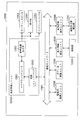
- FIG. 1 is a block diagram illustrating a functional configuration example of the solid-state imaging device 101 according to the first embodiment of the present technology.
- the solid-state imaging device 101 is a so-called global shutter-type back-illuminated image sensor such as a CMOS (Complementary Metal Oxide Semiconductor) image sensor.
- the solid-state imaging device 101 receives light from a subject, performs photoelectric conversion, and generates an image signal to capture an image.
- CMOS Complementary Metal Oxide Semiconductor
- the global shutter method is basically a global exposure method that starts exposure at the same time for all pixels and ends exposure at the same time for all pixels.
- all pixels means all of the pixels appearing in the image, and dummy pixels and the like are excluded.
- the global shutter method includes a method in which global exposure is performed on pixels in a predetermined area instead of all the pixels in the portion appearing in the image.
- a back-illuminated image sensor is a photoelectric converter such as a photodiode that receives light from a subject and converts it into an electrical signal.
- the solid-state imaging device 101 includes, for example, a pixel array unit 111, a vertical driving unit 112, a ramp wave module 113, a column signal processing unit 114, a clock module 115, a data storage unit 116, a horizontal driving unit 117, a system control unit 118, and a signal.
- a processing unit 119 is provided.
- the pixel array unit 111 is formed on the semiconductor substrate 11 (described later). Peripheral circuits such as the vertical driving unit 112 to the signal processing unit 119 are formed on the same semiconductor substrate 11 as the pixel array unit 111, for example.
- the pixel array unit 111 includes a plurality of sensor pixels 121 including photoelectric conversion elements that generate and accumulate charges according to the amount of light incident from the subject. As shown in FIG. 1, the sensor pixels 121 are arranged in each of the horizontal direction (row direction) and the vertical direction (column direction). In the pixel array unit 111, pixel drive lines 122 are wired along the row direction for each pixel row composed of sensor pixels 121 arranged in one column in the row direction, and are composed of sensor pixels 121 arranged in one column in the column direction. For each pixel column, a vertical signal line 123 is wired along the column direction.
- the vertical drive unit 112 includes a shift register, an address decoder, and the like.
- the vertical drive unit 112 supplies signals and the like to the plurality of sensor pixels 121 via the plurality of pixel drive lines 122 to drive all the plurality of sensor pixels 121 in the pixel array unit 111 at the same time, or Drive line by line.
- the ramp wave module 113 generates a ramp wave signal used for A / D (Analog / Digital) conversion of the pixel signal and supplies it to the column signal processing unit 114.
- the column signal processing unit 114 includes, for example, a shift register and an address decoder, and performs a noise removal process, a correlated double sampling process, an A / D conversion process, and the like to generate a pixel signal.
- the column signal processing unit 114 supplies the generated pixel signal to the signal processing unit 119.
- the clock module 115 supplies a clock signal for operation to each part of the solid-state imaging device 101.
- the horizontal drive unit 117 sequentially selects unit circuits corresponding to the pixel columns of the column signal processing unit 114. By the selective scanning by the horizontal driving unit 117, the pixel signals subjected to signal processing for each unit circuit in the column signal processing unit 114 are sequentially output to the signal processing unit 119.
- the system control unit 118 includes a timing generator that generates various timing signals.
- the system control unit 118 performs drive control of the vertical drive unit 112, the ramp wave module 113, the column signal processing unit 114, the clock module 115, and the horizontal drive unit 117 based on the timing signal generated by the timing generator. is there.
- the signal processing unit 119 performs signal processing such as arithmetic processing on the pixel signal supplied from the column signal processing unit 114 while temporarily storing data in the data storage unit 116 as necessary, and outputs each pixel signal. Is output.
- FIG. 2 shows a circuit configuration example of one sensor pixel 121 of the pixel array unit 111.
- the sensor pixel 121 in the pixel array unit 111 includes a photoelectric conversion unit 51, a first transfer transistor (TRX) 52, a second transfer transistor (TRM) 53, a charge holding unit (MEM) 54, and a third transfer. It includes a transistor (TRG) 55, a charge-voltage converter (FD) 56, a discharge transistor (OFG) 57, a reset transistor (RST) 58, an amplification transistor (AMP) 59, and a selection transistor (SEL) 60.
- TRG transistor
- FD charge-voltage converter
- OFFG discharge transistor
- RST reset transistor
- AMP amplification transistor
- SEL selection transistor
- TRX52, TRM53, TRG55, OFG57, RST58, AMP59, and SEL60 are all N-type MOS transistors.
- Drive signals S52, S53, S55, S57, S58, and S60 are supplied to the gate electrodes of TRX52, TRM53, TRG55, OFG57, RST58, and SEL60, respectively.
- the drive signals S52, S53, S55, S57, S58, and S60 are pulse signals in which a high level state is an active state (on state) and a low level state is an inactive state (off state).
- setting the drive signal to the active state is also referred to as turning on the drive signal
- setting the drive signal to the inactive state is also referred to as turning off the drive signal.
- the photoelectric conversion unit 51 is a photoelectric conversion element made of, for example, a PN junction photodiode, and receives light from the subject, generates electric charge according to the amount of received light by photoelectric conversion, and accumulates it.
- the TRX 52 is connected between the photoelectric conversion unit 51 and the TRM 53, and transfers charges accumulated in the photoelectric conversion unit 51 to the MEM 54 in response to a drive signal S52 applied to the gate electrode of the TRX 52. is there.
- the TRM 53 controls the potential of the MEM 54 in accordance with the drive signal S53 applied to the gate electrode of the TRM 53. For example, when the drive signal S53 is turned on and the TRM 53 is turned on, the potential of the MEM 54 is deepened. Further, when the drive signal S53 is turned off and the TRM 53 is turned off, the potential of the MEM 54 becomes shallow. When the drive signal S52 and the drive signal S53 are turned on and the TRX 52 and the TRM 53 are turned on, the charges accumulated in the photoelectric conversion unit 51 are transferred to the MEM 54 via the TRX 52 and the TRM 53.
- the MEM 54 is an area that temporarily holds charges accumulated in the photoelectric conversion unit 51 in order to realize a global shutter function.
- the TRG 55 is connected between the TRM 53 and the FD 56, and transfers the electric charge held in the MEM 54 to the FD 56 in accordance with the drive signal S55 applied to the gate electrode of the TRG 55. For example, when the drive signal S53 is turned off, the TRM 53 is turned off, the drive signal S55 is turned on, and the TRG 55 is turned on, the charge held in the MEM 54 is transferred to the FD 56 via the TRM 53 and the TRG 55. ing.
- the FD 56 is a floating diffusion region that converts the electric charge transferred from the MEM 54 via the TRG 55 into an electric signal (for example, a voltage signal) and outputs the electric signal.
- An RST 58 is connected to the FD 56 and a vertical signal line VSL is connected via the AMP 59 and the SEL 60.
- the OFG 57 has a drain connected to the power supply VDD and a source connected to the wiring between the TRX 52 and the TRM 53.
- the OFG 57 initializes, that is, resets the photoelectric conversion unit 51 in accordance with the drive signal S57 applied to the gate electrode. For example, when the drive signal S52 and the drive signal S57 are turned on and the TRX 52 and the OFG 57 are turned on, the potential of the photoelectric conversion unit 51 is reset to the voltage level of the power supply VDD. That is, the photoelectric conversion unit 51 is initialized.
- the OFG 57 forms an overflow path between the TRX 52 and the power supply VDD, and discharges the electric charge overflowing from the photoelectric conversion unit 51 to the power supply VDD.
- the RST 58 has a drain connected to the power supply VDD and a source connected to the FD 56.
- the RST 58 initializes, that is, resets each region from the MEM 54 to the FD 56 in accordance with the drive signal S58 applied to the gate electrode. For example, when drive signal S55 and drive signal S58 are turned on and TRG55 and RST58 are turned on, the potentials of MEM 54 and FD 56 are reset to the voltage level of power supply VDD. That is, initialization of the MEM 54 and the FD 56 is performed.
- the AMP 59 has a gate electrode connected to the FD 56 and a drain connected to the power supply VDD, and serves as an input unit of a source follower circuit that reads out electric charges obtained by photoelectric conversion in the photoelectric conversion unit 51. That is, the source of the AMP 59 is connected to the vertical signal line VSL via the SEL 60, thereby forming a source follower circuit together with a constant current source connected to one end of the vertical signal line VSL.
- the pixel circuit illustrated in FIG. 2 is an example of a pixel circuit that can be used in the pixel array unit 111, and a pixel circuit having another configuration can also be used.
- the transistors RST58, AMP59, and SEL60 are referred to as pixel transistors.
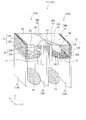
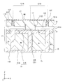
- FIG. 3 is a perspective view schematically showing the configuration of any two adjacent sensor pixels 121A and 121B in the solid-state imaging device 101.
- FIG. 4A and 4B are cross-sectional views schematically showing the configuration of the sensor pixels 121A and 121B, respectively.
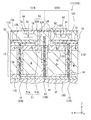
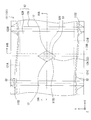
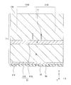
- FIG. 5A is a plan view schematically showing the entire configuration of the pixel array unit 111.
- FIG. 5B is an enlarged plan view showing a partial region of the pixel array unit 111, and schematically shows the configuration of four sensor pixels 121A to 121D adjacent to each other.
- the shape of the light shielding portion 12 (described later) is mainly indicated by a solid line, and other components are partially omitted.
- P and N in the figure represent a P-type semiconductor region and an N-type semiconductor region, respectively.
- “+” or “ ⁇ ” at the end of each symbol of “P ++”, “P +”, “P ⁇ ”, and “P ⁇ ” represents the impurity concentration of the P-type semiconductor region.
- “+” or “ ⁇ ” at the end of each symbol “N ++”, “N +”, “N ⁇ ”, and “N ⁇ ” represents the impurity concentration of the N-type semiconductor region.
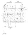
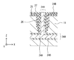
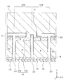
- the solid-state imaging device 101 includes a semiconductor substrate 11, a photoelectric conversion unit 51 embedded in the semiconductor substrate 11, a TRX 52, a TRM 53, a MEM 54, a TRG 55, an OFG 57, an opaque unit 12, and an element isolation unit 13. , An etching stopper 17, a color filter CF, and a light receiving lens LNS.
- the back surface 11B (FIGS. 4A and 4B) is the light receiving surface.
- the semiconductor substrate 11 is made of, for example, a Si ⁇ 111 ⁇ substrate.
- the Si ⁇ 111 ⁇ substrate is a single crystal silicon substrate having a ⁇ 111 ⁇ crystal orientation.
- the semiconductor substrate 11 has a back surface 11B that is a light receiving surface that receives light from a subject that has passed through the light receiving lens LNS and the color filter CF, and a surface 11A opposite to the back surface 11B.
- the photoelectric conversion unit 51 includes, for example, an N ⁇ type semiconductor region 51A and an N type semiconductor region 51B in order from a position close to the back surface 11B.
- the light incident on the back surface 11B is photoelectrically converted in the N ⁇ type semiconductor region 51A to generate charges, and then the charges are accumulated in the N type semiconductor region 51B.
- the boundary between the N ⁇ type semiconductor region 51A and the N type semiconductor region 51B is not always clear.
- the N type impurity concentration gradually increases from the N ⁇ type semiconductor region 51A toward the N type semiconductor region 51B. Just do it.
- the light shielding unit 12 is a member that functions to prevent light from entering the MEM 54, and is provided so as to surround the MEM 54.
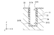
- the light shielding unit 12 is provided on the opposite side of the back surface 11B of the semiconductor substrate 11 as viewed from the photoelectric conversion unit 51, for example, and spreads along a horizontal plane (XY plane), and the horizontal light shielding portion.
- a vertical light shielding portion 12V extending along the YZ plane so as to be orthogonal to 12H.
- the vertical light shielding portion 12 ⁇ / b> V is a wall portion that is provided at a boundary portion between the sensor pixels 121 adjacent in the X-axis direction in plan view and extends in the Y-axis direction.
- the vertical light shielding portion 12V is exposed on the surface 11A of the Si ⁇ 111 ⁇ substrate. Further, the horizontal light shielding portion 12H is located between the photoelectric conversion unit 51 and the MEM 54 in the Z-axis direction as shown in FIG. 4, and the pixel array except for the opening 12K as shown in FIGS. 5A and 5B.
- the portion 111 is provided over the entire XY plane. The light that has entered from the back surface 11 ⁇ / b> B and has not been absorbed by the photoelectric conversion unit 51 but transmitted through the photoelectric conversion unit 51 is reflected by the horizontal light shielding portion 12 ⁇ / b> H of the light shielding unit 12 and is incident on the photoelectric conversion unit 51 again.
- the horizontal light shielding portion 12H includes a pair of first surfaces S1, a pair of second surfaces S2, and a third surface S3.
- the pair of first surfaces S1 are surfaces along the first crystal surface 11S1 of the semiconductor substrate 11, and face each other in the Z-axis direction (see FIGS. 4A and 4B).
- the first crystal face 11S1 in the semiconductor substrate 11 is represented by a plane index ⁇ 111 ⁇ .
- the pair of second surfaces S2 are surfaces along the second crystal surface 11S2 of the semiconductor substrate 11, and are located at both ends of the pixel array unit 111 in the Y-axis direction (see FIG. 4B).
- the second crystal plane 11S2 of the semiconductor substrate is not in the effective pixel region but in the peripheral pixel region surrounding it. For example, in FIG.
- the second crystal plane 11S2 in the semiconductor substrate 11 is represented by a plane index ⁇ 111 ⁇ , and is inclined by about 19.5 ° with respect to the Z-axis direction. That is, the inclination angle of the second crystal plane 11S2 with respect to the horizontal plane (XY plane) is about 70.5 °. As shown in FIGS. 5A and 5B, the second crystal plane 11S2 is inclined with respect to the X axis and the Y axis on the horizontal plane (XY plane), for example, about 30 ° with respect to the Y axis. It makes an angle.
- the light shielding portion 12 has a two-layer structure of an inner layer portion 12A and an outer layer portion 12B surrounding the periphery thereof.
- the inner layer portion 12A is made of, for example, a material containing at least one of a single metal having a light shielding property, a metal alloy, a metal nitride, and a metal silicide. More specifically, the constituent material of the inner layer portion 12A includes Al (aluminum), Cu (copper), Co (cobalt), W (tungsten), Ti (titanium), Ta (tantalum), Ni (nickel).
- the inner layer portion 12A may be made of graphite or an organic material.
- the outer layer portion 12B is made of an insulating material such as SiOx (silicon oxide). The outer layer portion 12B ensures electrical insulation between the inner layer portion 12A and the semiconductor substrate 11.
- the element isolation part 13A is in contact with the horizontal light shielding part 12H, for example.
- a part of the element isolation portion 13B penetrates the opening 12K in the Z-axis direction and protrudes to the surface 11A side from the horizontal light shielding portion 12H.
- Etching stoppers 17 are provided at both ends of the opening 12K in the X-axis direction.
- the etching stopper 17 has a function of hindering the progress of etching when the horizontal light shielding portion 12H is formed by wet etching.
- the etching stopper 17 exhibits etching resistance with respect to an etching solution capable of etching the semiconductor substrate 11 in the ⁇ 110> direction, for example, an alkaline aqueous solution.
- an impurity element such as B (boron)
- a crystal defect structure in which hydrogen ions are implanted or an insulator such as an oxide can be used.
- Each gate electrode in TRX 52, TRM 53, TRG 55, and OFG 57 is provided on the surface 11 A of the semiconductor substrate 11 via the insulating layer 18. Further, the MEM 54 which is an N-type semiconductor region is embedded in the semiconductor substrate 11 and is disposed between the surface 11A and the horizontal light shielding portion 12H. Further, a P-type semiconductor region 16 is provided between the MRM 54 and the surface 11A.
- the solid-state imaging device 101 further includes a P-type semiconductor region 14 provided along the side surface of the element isolation unit 13 between the element isolation unit 13 and the photoelectric conversion unit 51.
- the solid-state imaging device 101 further includes a fixed charge film 15 provided between the photoelectric conversion unit 51 and the back surface 11B.
- the fixed charge film 15 is exposed on the back surface 11B.
- the fixed charge film 15 has a negative fixed charge in order to suppress the generation of dark current due to the interface state of the back surface 11 ⁇ / b> B that is the light receiving surface of the semiconductor substrate 11.
- a hole accumulation layer is formed in the vicinity of the back surface 11 ⁇ / b> B of the semiconductor substrate 11 by the electric field induced by the fixed charge film 15. The hole accumulation layer suppresses generation of electrons from the back surface 11B.
- the color filter CF is provided in contact with the fixed charge film 15.
- the light receiving lens LNS is located on the side opposite to the fixed charge film 15 when viewed from the color filter CF, and is provided so as to be in contact with the color filter CF.
- the surface 11A of the semiconductor substrate 11 is prepared.
- a hard mask HM that selectively covers is formed.
- the hard mask HM has an opening K at a position where the vertical light shielding portion 12V of the light shielding portion 12 is to be formed, and is made of an insulating material such as SiN (silicon nitride) or SiO 2 (silicon oxide).
- the etching stopper 17 is formed by, for example, forming a trench having a predetermined depth from the surface 11A of the semiconductor substrate 11 at a predetermined position and then filling the trench with an insulator such as an oxide.
- the vertical light shielding portion 12 ⁇ / b> V is formed by digging out the exposed portion of the Si ⁇ 111 ⁇ constituting the semiconductor substrate 11 in the opening K by dry etching using the hard mask HM.
- a trench 12T is formed at a predetermined position.
- the depth of the trench 12T at this time corresponds to the dimension in the Z-axis direction of the vertical light shielding portion 12V to be formed later.
- wet etching is performed on the semiconductor substrate 11, which will be described later, since the etching process slightly proceeds in the ⁇ 111> direction, the depth of the trench 12T may be adjusted in consideration of this.
- a sidewall SW is formed so as to cover the side surface and the bottom surface of the trench 12T.
- an insulating film made of, for example, SiN or SiO 2 is formed so as to cover the inner surface of the trench 12T, that is, the side surface 12TA and the bottom surface 12TB of the trench 12T, and then the trench 12T is formed by dry etch back. Only the insulating film covering the bottom surface 12TB is removed.
- the constituent material of the sidewall SW may be different from the constituent material of the hard mask HM.
- part of Si ⁇ 111 ⁇ constituting the semiconductor substrate 11 is removed by dry etching back so as to further dig up the bottom surface 12TB of the trench 12T.
- the bottom surface 12TB is further dug down by a depth corresponding to the thickness of the horizontal light shielding portion 12H.
- wet etching is performed on the semiconductor substrate 11 to be described later, since the etching process slightly proceeds in the ⁇ 111> direction, the digging depth from the bottom surface 12TB of the trench 12T is adjusted in consideration of this. Good. This process need not be performed.
- a predetermined alkaline aqueous solution is injected into the trench 12T and wet etching is performed to partially remove Si ⁇ 111 ⁇ constituting the semiconductor substrate 11.
- KOH, NaOH, CsOH or the like can be applied if it is an inorganic solution, and if it is an organic solution, EDP (ethylenediamine pyrocatechol aqueous solution), N 2 H 4 (hydrazine), NH 4 OH (hydroxylation). Ammonium), TMAH (tetramethylammonium hydroxide), and the like are applicable.
- the distance of the etching progress in the ⁇ 110> direction can be adjusted by the etching time of the semiconductor substrate 11 with the aqueous alkali solution.
- the etching stopper 17 in advance at a predetermined position as in the present embodiment, the progress of etching in the ⁇ 110> direction can be easily controlled, and the region where Si ⁇ 111 ⁇ remains can be accurately determined. It can be secured.
- FIG. 5B shows a state where the four third crystal faces 11S3 spreading from the two etching stoppers 17 as base points form a rhombus in plan view.
- the rhombic region surrounded by the four third crystal faces 11S3 is the Si remaining region 22 where Si ⁇ 111 ⁇ remaining finally surrounded by the horizontal light shielding portion 12H of the light shielding portion 12 remains.
- the second crystal face 11S2 is also formed.
- the hard mask HM and the sidewall SW are removed by, for example, wet etching.
- the hard mask HM and the sidewall SW can be removed by isotropic dry etching.
- a chemical solution containing HF (hydrofluoric acid) such as DHF (dilute hydrofluoric acid) or BHF (buffered hydrofluoric acid) is used, and the hard mask HM or the like is used.
- HF hydrofluoric acid
- BHF biuffered hydrofluoric acid
- a chemical solution containing hot phosphoric acid or HF may be used.
- the hard mask HM and the sidewall SW need not be removed.
- the outer layer portion 12B is formed using an insulating material or the like so as to cover the side surface 12TA of the trench 12T and the inner surface of the space 12Z and the surface 11A of the semiconductor substrate 11, and the inner layer so as to fill the trench 12T and the space 12Z. Fill portion 12A.
- the light shielding part 12 including the vertical light shielding part 12V occupying the trench 12T and the horizontal light shielding part 12H occupying the space 12Z is formed.
- the width of the trench 12T dimension in the X-axis direction
- the thickness of the space 12Z dimension in the Z-axis direction).
- the inner layer portion 12A is filled with the above-described metal material at this stage, it is difficult to perform a process involving a high temperature thereafter. Therefore, after temporarily filling the trench 12T and the space 12Z using a temporary filling material having relatively high heat resistance such as SiO 2 , SiN, or polysilicon, After the step of forming the element isolation portion 13 is completed, it may be replaced with a predetermined metal material.
- a temporary filling material having relatively high heat resistance such as SiO 2 , SiN, or polysilicon
- the vertical light shielding portion 12V is provided at the boundary position between the sensor pixels 121. For this reason, it is possible to prevent light leaking from one sensor pixel 121 to another sensor pixel 121 adjacent thereto from entering the photoelectric conversion unit 51 of the other sensor pixel 121 and generating noise such as color mixing. it can.
- the horizontal light-shielding portion 12H that is positioned between the photoelectric conversion unit 51 and the MEM 54 in the thickness direction and extends along the horizontal plane is provided. For this reason, in each sensor pixel 121, it can prevent that the light which permeate
- the horizontal light shielding portion 12H is provided inside the semiconductor substrate 11 which is a Si ⁇ 111 ⁇ substrate.
- the horizontal light shielding portion 12H includes a first surface S1 along the first crystal surface 11S1 and a second surface S2 along the second crystal surface 11S2 inclined with respect to the first surface S1. Yes.
- both the first crystal face 11S1 and the second crystal face 11S2 are represented by a plane index ⁇ 111 ⁇ . Accordingly, the horizontal light shielding portion 12H can be easily formed by crystal anisotropic etching using an etching solution such as an alkaline aqueous solution and has high dimensional accuracy.
- the etching stopper 17 is provided in advance, the controllability at the time of crystal anisotropic etching is improved, and the horizontal light-shielding portion 12H having higher dimensional accuracy is provided. It is easily obtained.
- the presence of the horizontal light-shielding portion 12H avoids the influence of the electric field generated in each transistor (for example, TRX52) in each sensor pixel 121 from reaching the photoelectric conversion unit 51. be able to. That is, it is possible to prevent a dark current generated by the electric field of each transistor from flowing into the photoelectric conversion unit 51 and generating noise.
- the channel mobility is higher than that in the case where the Si (100) substrate is used, and the charge transfer characteristics are improved. Improvement can be expected.
- the anisotropic crystal etching using the alkaline aqueous solution is performed on the Si ⁇ 111 ⁇ substrate when forming the light shielding portion 12, high controllability is achieved. Is obtained.
- FIG. 7 is an enlarged plan view showing a partial region of the pixel array unit 111 in the solid-state imaging device 102 according to the second embodiment of the present technology.
- the configuration of four sensor pixels 121A to 121D that are close to each other. Is schematically represented.
- FIG. 7 corresponds to FIG. 5B of the first embodiment, and the shape of the light shielding part 12 is mainly indicated by a solid line.
- the horizontal light shielding portion 12H in the light shielding portion 12 forms the opening 12K and has the island-like Si remaining region 22.
- the light shielding unit 12 is separated by the strip-like Si remaining region 23 extending in the X-axis direction. Further, the solid-state imaging device 102 according to the present embodiment does not have the etching stopper 17. Except for these points, the other configuration is substantially the same as that of the solid-state imaging device 101 according to the first embodiment.
- the solid-state imaging device 102 according to the present embodiment can form the horizontal light shielding portion 12H in the light shielding portion 12 without using the etching stopper 17, the manufacturing process can be simplified. Moreover, since the area of the Si remaining region 23 is larger than the area of the Si remaining region 22 of the solid-state imaging device 101 according to the first embodiment, the mechanical strength when forming the space 12Z can be increased. it can. However, the solid-state imaging device 101 is more advantageous than the solid-state imaging device 102 in terms of light shielding properties.
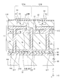
- FIG. 8 is an enlarged plan view showing a partial region of the pixel array unit 111 in the solid-state imaging device 103 according to the third embodiment of the present technology.
- the configuration of four sensor pixels 121A to 121D that are close to each other. Is schematically represented.
- FIG. 8 corresponds to FIG. 5B of the first embodiment, and the shapes of the light shielding part 12 and the light shielding part 24 (described later) are mainly shown by solid lines.
- 9A represents a cross section taken along the line IXA-IXA shown in FIG. 8
- FIG. 9B represents a cross section taken along the line IXB-IXB shown in FIG.
- FIG. 10 is a perspective view schematically showing the configuration of any two adjacent sensor pixels 121A and 121B in the solid-state imaging device 103, and corresponds to FIG. 3 of the first embodiment. .
- the solid-state imaging device 103 according to the present embodiment further includes a light shielding unit 24 in addition to the light shielding unit 12. Except for this point, the other configuration is substantially the same as that of the solid-state imaging device 102 according to the second embodiment.
- the light shielding part 24 is provided in the Si remaining region 23 where Si ⁇ 111 ⁇ remains in the layer where the light shielding part 12 is provided.
- the light shielding unit 24 includes a horizontal light shielding part 24H extending along the horizontal plane (XY plane) and a vertical light shielding part 24V extending along the YZ plane so as to be orthogonal to the horizontal light shielding part 24H. It is out.
- the vertical light-shielding portion 12V is a wall portion on the extension of the vertical light-shielding portion 12V in the Y-axis direction, and is provided at the boundary portion between the sensor pixels 121 adjacent in the X-axis direction in plan view. It has been.
- the horizontal light shielding portion 24H is located at a deep position away from the surface 11A in the Z-axis direction, that is, below the vertical terminal portion 52V in the Z-axis direction. As shown in FIG. 8, the horizontal light shielding portion 24 ⁇ / b> H extends in the X-axis direction in a strip shape so as to occupy a region corresponding to the Si remaining region 23. The light that is incident from the back surface 11B and is transmitted through the photoelectric conversion unit 51 without being absorbed by the photoelectric conversion unit 51 is reflected by the horizontal light shielding portion 24H of the light shielding unit 24 and is incident on the photoelectric conversion unit 51 again.
- the horizontal light-shielding portion 24H of the light-shielding portion 24 also functions as a reflector, similarly to the horizontal light-shielding portion 12H, and functions to prevent light that has passed through the photoelectric conversion portion 51 from entering the MEM 54 and generating noise.
- the horizontal light shielding portion 24H includes a pair of fourth surfaces S4 and a pair of fifth surfaces S5.
- the pair of fourth surfaces S4 are surfaces along the fourth crystal surface 11S4 of the semiconductor substrate 11, and face each other in the Z-axis direction (see FIGS. 9A to 9C).
- the fourth crystal plane 11S4 in the semiconductor substrate 11 is represented by a plane index ⁇ 111 ⁇ .
- the pair of fifth surfaces S5 are surfaces along the fifth crystal surface 11S5 of the semiconductor substrate 11, and are located at both ends in the Y-axis direction of the pixel array unit 111 (see FIG. 9C).
- the fifth crystal plane 11S5 in the semiconductor substrate 11 is represented by a plane index ⁇ 111 ⁇ , and is inclined by about 19.5 ° with respect to the Z-axis direction. That is, the inclination angle of the fifth crystal plane 11S5 with respect to the horizontal plane (XY plane) is, for example, about 70.5 °.
- An insulating layer 25 is provided around the vertical light shielding portion 12V, and insulating layers 25 to 27 are provided around the vertical light shielding portion 24V.
- the insulating layers 25 to 27 are used as masks when the light shielding part 12 and the light shielding part 24 are processed.
- FIGS. 11A to 11D and FIGS. 12A to 12D a process of forming the light shielding portion 12 and the light shielding portion 24 will be described.
- 11A to 11D are cross-sectional views showing the main part of the process of forming the light shielding part 12, and correspond to FIG. 9A.
- 12A to 12D are cross-sectional views of relevant parts showing the formation process of the light shielding portion 24, and correspond to FIG. 9B.
- the trench 12T is formed at the position where the vertical light shielding portion 12V is to be formed, and the vertical light shielding portion.
- a trench 24T is formed at a position where 24V is to be formed.
- Si ⁇ 111 ⁇ constituting the semiconductor substrate 11 is partially removed by dry etching back using the insulating layer 25 as a hard mask. .
- the depth of the trench 12T at this time becomes the dimension in the Z-axis direction of the vertical light shielding portion 12V to be formed later.
- the insulating layer 25 is further formed so as to cover the side surface 12TA and the bottom surface 12TB of the trench 12T and the side surface 24TA and the bottom surface 24TB of the trench 24T. After that, only the portion of the insulating layer 25 that covers the bottom surfaces 12TB and 24TB is removed by dry etch back.
- Si ⁇ 111 ⁇ constituting the semiconductor substrate 11 is partially removed by dry etching back so as to further dig up the bottom surface 12TB of the trench 12T and the bottom surface 24TB of the trench 24T, respectively.
- the insulating layer 26 is formed over the entire surface so as to fill the trench 12T and the trench 24T, and then a resist mask RM is formed by photolithography so as to selectively cover the portion of the insulating layer 26 where the trench 12T is filled.
- a resist mask RM is formed by photolithography so as to selectively cover the portion of the insulating layer 26 where the trench 12T is filled.
- a part of the insulating layer 26 filling the trench 24T not covered with the resist mask RM is removed by dry etch back.
- the insulating layer 26 remains only in the portion covering the side surface 24TA of the trench 24T, and Si ⁇ 111 ⁇ is exposed on the bottom surface 24TB of the trench 24T (FIG. 11A).
- the insulating layer 25 and the insulating layer 26 are both made of an insulating material such as SiO 2 or SiN. However, the insulating layer 25 and the insulating layer 26 are preferably made of different materials.
- the resist mask RM is removed.
- Si ⁇ 111 ⁇ exposed on the bottom surface 24TB of the trench 24T not covered with the insulating layer 26 is further dug down by dry etch back.
- the insulating layer 27 is further formed by the CVD method, for example, using the same material as the insulating layer 25, and the insulating layer 27 covering the bottom surface TB is removed by dry etching back.
- Si ⁇ 111 ⁇ exposed on the bottom surface 24TB of the trench 24T is subjected to crystal anisotropic etching using an alkaline aqueous solution in the same manner as in the first embodiment, thereby forming a space. 24Z is formed.
- the insulating layer 26 filling the trench 12T is dissolved and removed by, for example, phosphoric acid, and then crystal anisotropic etching using an alkaline aqueous solution is performed to form the space 12Z. .
- the outer layer portion 12B is formed using an insulating material or the like so as to cover the insulating layer 25 and the inner surface of the space 12Z, and the inner layer portion 12A is filled so as to fill the trench 12T and the space 12Z.
- the light shielding part 12 including the vertical light shielding part 12V occupying the trench 12T and the horizontal light shielding part 12H occupying the space 12Z is formed.
- the outer layer 24B is formed using an insulating material or the like so as to cover the insulating layer 27 and the inner surface of the space 24Z, and the inner layer 24A is filled so as to fill the trench 24T and the space 24Z.
- the light shielding part 24 including the vertical light shielding part 24V occupying the trench 24T and the horizontal light shielding part 24H occupying the space 24Z is formed.
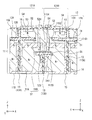
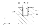
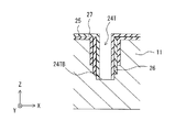
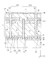
- FIG. 13 is an enlarged cross-sectional view illustrating a partial region of the pixel array unit 111 in the solid-state imaging device 104 according to the fourth embodiment of the present technology.
- FIG. 13 corresponds to FIG. 4A of the first embodiment, and mainly shows the structure of the sensor pixel 121A.
- the solid-state imaging device 101 includes the element isolation unit 13 formed from the back surface 11B.
- the light shielding unit and the element separation unit are integrated. That is, in the solid-state imaging device 104, a vertical light shielding portion 31V extending in the Z-axis direction from the front surface 11A to the back surface 11B of the semiconductor substrate 11 and a horizontal light shielding extending in a horizontal plane so as to be orthogonal to the vertical light shielding portion 31V.
- the light shielding part 31 including the part 31H is provided.
- the light shielding portion 31 has a two-layer structure of an inner layer portion 31A and an outer layer portion 31B surrounding the periphery.
- the inner layer portion 31A and the outer layer portion 31B are made of the same material as the inner layer portion 12A and the outer layer portion 12B, for example. Further, a solid phase diffusion layer 19 including a P-type region and an N-type region is formed around the light shielding portion 31.
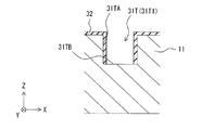
- FIGS. 14A to 14H are cross-sectional views of relevant parts showing the steps of forming the light shielding part 31 and the solid phase diffusion layer 19, and correspond to FIG.
- the trench 31T (31T1) is formed at the position where the vertical light shielding portion 31V is to be formed, in the same manner as the solid-state imaging device 103 of the third embodiment.
- Si ⁇ 111 ⁇ constituting the semiconductor substrate 11 is dry-etched using the insulating layer 32 as a hard mask. Part is removed by bag.
- the depth of the trench 31T1 at this time is the dimension in the Z-axis direction at a portion above the horizontal light shielding portion 31H in the vertical light shielding portion 31V to be formed later.
- an insulating layer 32 is further formed so as to cover side surface 31TA and bottom surface 31TB of trench 31T1. After that, only the portion of the insulating layer 32 covering the bottom surface 31TB is removed by dry etch back.
- Si ⁇ 111 ⁇ constituting the semiconductor substrate 11 is partially removed by dry etch back so as to further dig up the bottom surface 31TB of the trench 31T1.
- an insulating layer 33 is formed entirely using, for example, SiN so as to fill the trench 31T1, and then part of the insulating layer 33 filling the trench 31T1 is removed by dry etch back.
- the insulating layer 33 remains only in the portion covering the side surface 31TA of the trench 31T1, and Si ⁇ 111 ⁇ is exposed on the bottom surface 31TB of the trench 31T1 (FIG. 14B).
- Si ⁇ 111 ⁇ constituting the semiconductor substrate 11 is partially removed by dry etch back so as to further dig up the bottom surface 31TB of the trench 31T1.
- a trench 31T2 communicating with the trench 31T1 is formed below the trench 31T1.
- Si ⁇ 111 ⁇ is exposed on the side and bottom surfaces of the trench 31T2.
- Si ⁇ 111 ⁇ exposed on the side and bottom surfaces of the trench 31T2 is heated and thermally oxidized to form an insulating layer 34 made of SiO 2 and the like that covers the side and bottom surfaces of the trench 31T2.
- the insulating layer 33 is dissolved and removed only with a portion covering the side surface 31TA, for example, with phosphoric acid.
- Si ⁇ 111 ⁇ is exposed in the gap between the insulating layer 32 and the insulating layer 34.
- a space 31Z is formed by performing crystal anisotropic etching using an alkaline aqueous solution on Si ⁇ 111 ⁇ exposed in the gap between the insulating layer 32 and the insulating layer 34. . After that, the insulating layer 32 and the insulating layer 34 are removed.
- an insulating layer 35 such as a SiO 2 film containing P (phosphorus) which is an N-type impurity element so as to cover the inner surfaces of the trenches 31T1 and 31T2 and the inner surface of the space 31Z.
- P (phosphorus) contained in the insulating layer 35 is solid-phase diffused into the inner surfaces of the trenches 31T1 and 31T2 and the inner surface of the space 31Z in the semiconductor substrate 11 by heat treatment.
- an insulating layer 36 such as a SiO 2 film containing B (boron) which is a P-type impurity element is formed so as to cover the N-type region 19A.
- B (boron) contained in the insulating layer 36 is solid-phase diffused toward the inner surfaces of the trenches 31T1 and 31T2 and the inner surface of the space 31Z by heat treatment.
- the P-type region 19B can be formed inside the N-type region 19A, and the solid phase diffusion layer 19 is obtained.
- the light shielding portion 31 is formed by sequentially forming the outer layer portion 31B and the inner layer portion 31A so as to fill the trenches 31T1 and 31T2 and the space 31Z covered with the solid phase diffusion layer 19.
- the solid-state imaging device 104 includes the light shielding unit 31 that performs light shielding on the MEM 54 and also functions as an element separation unit that separates adjacent photoelectric conversion units 51.
- the manufacturing process can be simplified.
- the solid-state imaging device 104 is provided with the solid phase diffusion layer 19 including a pn junction around the light shielding portion 31 extending from the front surface 11A to the back surface 11B, an improvement in the pixel capacitance Qs can be expected.
- FIG. 15 is an enlarged plan view showing a partial region of the pixel array unit 111 in the solid-state imaging device 104A as a modification of the fourth embodiment, and the configuration of four sensor pixels 121A to 121D adjacent to each other. Is schematically represented.
- FIG. 15 corresponds to FIG. 5B of the first embodiment, and the shape of the light shielding portion 31 is mainly indicated by a solid line.
- the solid-state imaging device 104A as the present modification has a strip-like Si remaining region 23 like the solid-state imaging device 102 shown in FIG.
- the solid-state imaging device 104 ⁇ / b> A only the vertical light shielding portion 31 ⁇ / b> V of the light shielding portion 31 is provided in the strip-shaped Si remaining region 23, and the horizontal light shielding portion 31 ⁇ / b> H extending in the horizontal plane does not exist in the strip-shaped Si remaining region 23. Except for this point, the other configuration is substantially the same as that of the solid-state imaging device 104 as the fourth embodiment.
- FIGS. 16A to 16D are cross-sectional views corresponding to the cross-section in the direction of the arrow along the line XVI-XVI shown in FIG.
- the method for forming the light shielding portion 31 formed in the region other than the band-like Si remaining region 23 is the same as that in the fourth embodiment, and is therefore omitted.
- the trench 31T (31T1) is formed at the position where the vertical light-shielding portion 31V is to be formed in the same manner as the solid-state imaging device 104 of the fourth embodiment.
- Si ⁇ 111 ⁇ constituting the semiconductor substrate 11 is dry-etched using the insulating layer 32 as a hard mask. Part is removed by bag.
- the depth of the trench 31T1 at this time is the dimension in the Z-axis direction at a portion above the horizontal light shielding portion 31H in the vertical light shielding portion 31V to be formed later.
- an insulating layer 32 is further formed so as to cover side surface 31TA and bottom surface 31TB of trench 31T1. After that, only the portion of the insulating layer 32 covering the bottom surface 31TB is removed by dry etch back.
- the Si ⁇ 111 ⁇ constituting the semiconductor substrate 11 is dry-etched back so as to further dig up the bottom surface 31TB of the trench 31T1.
- the operation to remove a part is performed.
- the trench 31T1 in the strip-like Si remaining region 23 is selectively protected by a resist mask so that the bottom surface 31TB of the trench 31T1 is not dug down.
- an insulating layer 33 is formed over the entire surface using, for example, SiN so as to fill the trench 31T1, and then the insulating layer filling the trench 31T1 by dry etching back. 33 is partially removed. As a result, the insulating layer 33 remains only in the portion covering the side surface 31TA of the trench 31T1, and Si ⁇ 111 ⁇ is exposed on the bottom surface 31TB of the trench 31T1 (FIG. 16B).
- Si ⁇ 111 ⁇ constituting the semiconductor substrate 11 is partially removed by dry etching back so as to further dig up the bottom surface 31TB of the trench 31T1.
- a trench 31T2 communicating with the trench 31T1 is formed below the trench 31T1.
- Si ⁇ 111 ⁇ is exposed on the side and bottom surfaces of the trench 31T2.
- Si ⁇ 111 ⁇ exposed on the side and bottom surfaces of the trench 31T2 is heated and thermally oxidized to form an insulating layer 34 made of SiO 2 and the like that covers the side and bottom surfaces of the trench 31T2.
- the insulating layer 33 is dissolved and removed only with a portion covering the side surface 31TA, for example, with phosphoric acid.
- the space 31Z is formed by performing the crystal anisotropic etching using the alkaline aqueous solution.
- Si ⁇ 111 ⁇ is not exposed in the strip-like Si remaining region 23, etching of Si ⁇ 111 ⁇ is not performed.
- FIGS. 14E to 14H the formation of the light-shielding portion 31 having only the vertical light-shielding portion 31V and not having the horizontal light-shielding portion 31H is completed in the band-shaped Si remaining region 23.
- the area of the Si remaining region 23 is larger than the area of the Si remaining region 22 of the solid-state imaging device 101 according to the first embodiment.
- the mechanical strength at the time of forming the space 31Z can be increased.
- the manufacturing of the solid-state imaging device 104A can be realized.
- FIG. 17 is a perspective view schematically illustrating a part of the configuration of any two adjacent sensor pixels 121A and 121B in the solid-state imaging device 105 according to the fifth embodiment of the present technology. This corresponds to FIG. 3 of the embodiment.
- FIG. 18 illustrates a cross-sectional configuration of the solid-state imaging device 105.
- the solid-state imaging device 105 has a three-dimensional structure in which three substrates, that is, a first substrate BP1, a second substrate BP2, and a third substrate BP3 are sequentially stacked.
- the first substrate BP1 is obtained by providing a plurality of sensor pixels 121 on the semiconductor substrate 11.
- the second substrate BP2 includes a semiconductor substrate 81 including the read circuit CR2, an insulating layer 82 in which the semiconductor substrate 81 is embedded and bonded to the first substrate BP1, and a wiring layer 83 bonded to the third substrate BP3. are doing.
- the second substrate BP2 further includes a through wiring 84 that connects the wiring layer 83 and the FD 56 in the sensor pixel 121 of the first substrate BP1.
- the logic circuit CR3 includes, for example, a vertical driving unit 112, a ramp wave module 113, a column signal processing unit 114, a clock module 115, a data storage unit 116, a horizontal driving unit 117, a system control unit 118, and a signal processing unit 119. ing.
- the sensor pixel 121 in the solid-state imaging device 105 has a light shielding part 72 instead of the light shielding part 12 and has an element separation part 73 instead of the element separation part 13. Except for these points, the sensor pixel 121 in the solid-state imaging device 105 has substantially the same configuration as the sensor pixel 121 in the solid-state imaging device 101.
- the light shielding portion 72 has a two-layer structure of, for example, an inner layer portion 72A and an outer layer portion 72B surrounding the periphery.
- the inner layer portion 72A is made of a material including at least one of a single metal having a light shielding property, a metal alloy, a metal nitride, and a metal silicide, for example.
- the outer layer portion 72B is a solid phase diffusion layer including a pn junction between a P-type region and an N-type region.
- the element isolation unit 73 is a wall-like member that extends in the Z-axis direction so as to penetrate the semiconductor substrate 11 at the boundary position between the adjacent sensor pixels 121 and surrounds the photoelectric conversion units 51.
- the sensor pixels 121 adjacent to each other are electrically separated from each other by the element separation unit 73.
- the element separation portion 73 provided at a position corresponding to the vertical light shielding portion 72V in the Z-axis direction is indicated as an element separation portion 73A and corresponds to the opening 72K in the Z-axis direction.
- a part including a part at a position where the element is located is indicated as an element isolation part 73B.
- the element isolation portion 73B includes a horizontal light shielding portion 73H that overlaps the region corresponding to the opening 72K in the Z-axis direction.
- FIGS. 19A to 19D are cross-sectional views showing the manufacturing process of the solid-state imaging device 105, and correspond to FIG.
- a semiconductor substrate 11 is prepared in which a photoelectric conversion unit 51, a P-type semiconductor region 14, a fixed charge film 15, and an etching stopper 17 are formed at predetermined positions.
- the light shielding part 72 is formed in the same manner as the light shielding part 12 of the solid-state imaging device 101 of the first embodiment.
- the inner layer portion 72A is formed of a temporary filling material such as polysilicon.
- the outer layer portion 72B which is a solid phase diffusion layer, is formed in the same manner as the solid phase diffusion layer 19 in the solid-state imaging device 104 of the fourth embodiment.
- TRX52, TRM53, MEM54, TRG55, and OFG57 are formed on the surface 11A of the semiconductor substrate 11 using a known method, and an insulating layer 82A covering them is formed.
- the second substrate lower part BP2-1 having the insulating layer 82B in which the semiconductor substrate 81 including the readout circuit CR2 is embedded is bonded to the upper surface of the insulating layer 82A.
- the insulating layer 82A is formed by bonding the insulating layer 82A and the insulating layer 82B.
- the through wiring 84 is further formed so as to penetrate the second substrate lower part BP2-1.
- a wiring layer 83 is formed on the second substrate lower part BP2-1.
- the second substrate BP2 is provided on the first substrate BP1.
- the semiconductor substrate 11 is thinned from the back surface 11B side.
- a third substrate BP3 is prepared, and the wiring layer 83 of the second substrate BP2 and the wiring layer 63 of the third substrate BP3 are bonded to face each other.
- the element isolation part 73 is formed from the back surface 11B side. Specifically, as shown in FIG. 19D, first, a length that extends in the Z-axis direction by digging down the semiconductor substrate 11 from the back surface 11B side at a position where the element isolation portion 73A and the element isolation portion 73B are to be formed. A hole K73A and a long hole K73B are respectively formed. At this time, the long hole K73A is formed so as to reach the light shielding portion 72. Subsequently, after removing the temporary filling material filled as the inner layer portion 72A, refilling with a material containing at least one of a single metal, a metal alloy, a metal nitride, and a metal silicide having light shielding properties.
- the formation of the long hole K73A and the formation of the long hole K73B are performed at the same time, and after that, the long hole K73A is refilled with the above-described light-shielding material, and the long hole K73B and the space 73Z have the above-described light shielding properties. It is desirable to perform the material filling at the same time. However, the formation of the long hole K73A and the formation of the long hole K73B may be performed separately, or the refilling operation for the long hole K73A and the filling operation for the long hole K73B may be performed separately. Good. Finally, the solid-state imaging device 105 is completed by joining the color filter CF and the light receiving lens LNS in order on the back surface 11B.
- the second substrate BP2 including the readout circuit CR2 and the third substrate BP3 including the logic circuit CR3 are formed separately from the first substrate BP1 including the sensor pixel 121.
- the first to third substrates BP1 to BP3 can be stacked. Therefore, since general-purpose products can be used for the read circuit CR2 and the logic circuit CR3, the degree of freedom in design is increased and the manufacturing cost can be expected to be reduced.
- the element separation unit 73 is also provided with a horizontal light shielding portion 73H. For this reason, the light-shielding property with respect to MEM54 and FD56 can be improved further. Also, the mechanical strength is improved. Furthermore, it is considered that charge transfer is performed more smoothly than in the configuration in which the two light shielding units 12 and the light shielding unit 24 are provided as in the solid-state imaging device 103 of the third embodiment.
- FIG. 20 is a perspective view schematically illustrating the configuration of any two adjacent sensor pixels 121A and 121B in the solid-state imaging device 106 according to the sixth embodiment of the present technology.
- FIG. 21 schematically illustrates a cross-sectional configuration of the sensor pixels 121A and 121B.
- an insulating layer is used as a hard mask HM that selectively covers the back surface 11B. 94 is formed.
- the trenches 91T and 91T and the space 91Z communicating with the trench 91T are formed at positions where the vertical light-shielding portion 91V and the element isolation portion 13 are to be formed, and an N-type region is formed on the outside.
- a solid phase diffusion layer 19 having a P-type region is formed.
- the trench 91T and the space 91Z are formed from the back surface 11B in the same manner as the trench 12T and the space 12Z in the first embodiment, and then the trench 13T is formed.
- the solid phase diffusion layer 19 is formed in the same manner as the solid-state imaging device 104 of the fourth embodiment.
- the back surface 11B of the semiconductor substrate 11 is joined to the temporary substrate 96 via the insulating layer 95, and the surface of the semiconductor substrate 11 is 11A is thinned.
- a material having relatively high heat resistance such as SiO 2 , SiN, or polysilicon is used for temporarily filling the trenches 13T and 91T and the space 91Z.
- TRX52, TRM53, MEM54, TRG55, and OFG57 are formed using a known method.
- FIG. 22E after removing the temporary substrate 96 and the insulating layer 95, as shown in FIG. 22F, the temporary filling material in the trenches 13T, 91T and the space 91Z is removed, and the trenches 13T, 13T, The outer layer portion 91B and the inner layer portion 91A are sequentially formed so as to fill 91T and the space 91Z. Thereby, the element isolation
- the solid-state imaging device 106 includes the vertical light-shielding portion 91V also serving as the element separation unit 13 and the horizontal light-shielding portion 91H without providing the vertical light-shielding portion 12V in the first embodiment.
- the light shielding part 91 is provided. For this reason, it becomes possible to improve the freedom degree of the layout in the surface 11A side of the semiconductor substrate 11.
- FIG. As an example, the formation region of the charge holding portion (MEM) 54 can be enlarged by the vertical light shielding portion 12V.
- the solid phase diffusion layer 19 including a pn junction is provided around the light shielding portion 91, an improvement in the pixel capacitance Qs can be expected.
- the solid-state imaging device 106A as the present modification is such that a light-shielding portion 93 is further provided in addition to the light-shielding portion 91, like the solid-state imaging device 103 shown in FIG. 9C and FIG. Except this point, the other configuration is substantially the same as that of the solid-state imaging device 106 according to the sixth embodiment.
- FIG. 23 shows a cross section of the solid-state imaging device 106A corresponding to the direction of the arrow along the line IXC-IXC shown in FIG.
- the light shielding part 93 similarly to the light shielding part 24 in the solid-state imaging device 103 according to the third embodiment, at least an Si remaining in which Si ⁇ 111 ⁇ remains in the opening provided with the horizontal light shielding part 91H of the light shielding part 91. It is provided in the region 23 (see FIG. 7).
- the light shielding portion 93 extends along the horizontal plane (XY plane), similarly to the horizontal light shielding portion 91H, and is orthogonal to the element isolation portion 13 in the present embodiment.
- the trenches 13T and 91T are formed.
- spaces 93AZ and 91Z communicating with trenches 13T and 91T, respectively, and solid phase diffusion layer 19 having an N-type region on the outside and a P-type region on the inside are formed.
- the space 93Z communicating with the trench 13T and the trench 93T and the space 91Z communicating with the trench 91T and the trench 91T are formed separately.
- the trench 13T and the space 93Z communicating with the trench 13T can be formed, for example, in the same manner as in the fourth embodiment.
- the back surface 11B of the semiconductor substrate 11 is joined to the temporary substrate 96 via the insulating layer 95, and the semiconductor substrate 11 The surface 11A is thinned.
- TRX52, TRM53, MEM54, TRG55, and OFG57 are formed using a known method. After that, after removing the temporary substrate 96 and the insulating layer 95, as shown in FIG.
- the temporary filling material in the trenches 13T and 91T and the spaces 91Z and 93Z is removed, and the outer layer portion 91B and the inner layer portion 91A are separated. Sequentially formed. Thereby, the element isolation
- FIG. 25 schematically illustrates a cross-sectional configuration of any two adjacent sensor pixels 121A and 121B in a solid-state imaging device 106B as a modification of the sixth embodiment.
- the solid-state imaging device 106B as the present modification is such that a light shielding portion 92 orthogonal to the horizontal light shielding portion 91H is further provided on the surface 11A side of the semiconductor substrate 11. Except this point, the other configuration is substantially the same as that of the solid-state imaging device 106 according to the sixth embodiment.
- the light shielding part 92 extends from the front surface 11 ⁇ / b> A to the back surface 11 ⁇ / b> B of the semiconductor substrate 11, is in contact with the horizontal light shielding part 91 ⁇ / b> H of the light shielding part 91, and is integrated with the light shielding part 91. That is, in the solid-state imaging device 106B of the present embodiment, as in the solid-state imaging device 104 of the fourth embodiment, a horizontal light-shielding portion that extends in the Z-axis direction from the front surface 11A to the back surface 11B of the semiconductor substrate 11.
- a solid phase diffusion layer 99 including a P-type region and an N-type region is formed around the light shielding portion 92.
- the solid phase diffusion layer 99 may have a configuration similar to that of the solid phase diffusion layer 19, or may include a different impurity concentration or impurity from the solid phase diffusion layer 19.
- a trench 92T is formed at a position where the vertical light shielding portion 91V is formed.
- the solid phase diffusion layer 19 is formed in the same manner as the solid-state imaging device 104 of the fourth embodiment.
- the trench 92T is temporarily filled, and the hard mask HM is removed.
- TRX52, TRM53, MEM54, TRG55, and OFG57 are formed using a known method.
- the temporary filling material in the trenches 13T, 91T, 92T and the space 91Z is removed, and the outer layer portion 91B is filled so as to fill the trenches 13T, 91T, 92T and the space 91Z.
- the inner layer portion 91A are sequentially formed.
- the light shielding portions 91 and 92 are collectively formed.
- the element isolation portion 13 (13B) is formed at the same time.
- the color filter CF and the light receiving lens LNS are sequentially joined on the back surface 11B, thereby completing the solid-state imaging device 106B.
- the light shielding portion 92 is further provided, and the trench 92T constituting the light shielding portion 92 is separately formed from the surface 11A side of the semiconductor substrate 11.
- the solid phase diffusion layer 99 having an impurity concentration different from that of the solid phase diffusion layer 19 can be formed around the trench 92T.
- the solid phase diffusion layer 99 including an impurity concentration and an impurity material suitable for the charge holding unit (MEM) 54 can be formed. Therefore, in addition to the effects of the fourth embodiment, it is possible to form an optimum profile for each.
- FIG. 27 schematically illustrates a cross-sectional configuration of any two adjacent sensor pixels 121A and 121B in a solid-state imaging device 106C as a modified example of the sixth embodiment.
- the solid-state imaging device 106C is a combination of the solid-state imaging device 106 according to the sixth embodiment and the solid-state imaging device 105 according to the fifth embodiment.
- the substrate BP1) has a three-dimensional structure in which a second substrate BP2 and a third substrate BP3 are sequentially stacked.
- the sensor substrate 121 includes the second substrate BP2 including the readout circuit CR2 and the third substrate BP3 including the logic circuit CR3.
- the first to third substrates BP1 to BP3 can be stacked after being formed separately from the first substrate BP1 including the first substrate BP1. Therefore, since general-purpose products can be used for the read circuit CR2 and the logic circuit CR3, the degree of freedom in design is increased and the manufacturing cost can be expected to be reduced.
- FIG. 28 is a block diagram illustrating a configuration example of a camera 2000 as an electronic apparatus to which the present technology is applied.
- the camera 2000 is an optical unit 2001 including a lens group, an imaging device (imaging device) 2002 to which the above-described solid-state imaging device 101 or the like (hereinafter referred to as the solid-state imaging device 101 or the like) is applied, and a camera signal processing circuit.
- a DSP (Digital Signal Processor) circuit 2003 is provided.
- the camera 2000 also includes a frame memory 2004, a display unit 2005, a recording unit 2006, an operation unit 2007, and a power supply unit 2008.
- the DSP circuit 2003, the frame memory 2004, the display unit 2005, the recording unit 2006, the operation unit 2007, and the power supply unit 2008 are connected to each other via a bus line 2009.
- the optical unit 2001 captures incident light (image light) from a subject and forms an image on the imaging surface of the imaging device 2002.
- the imaging device 2002 converts the amount of incident light imaged on the imaging surface by the optical unit 2001 into an electrical signal for each pixel and outputs the electrical signal as a pixel signal.
- the display unit 2005 includes a panel type display device such as a liquid crystal panel or an organic EL panel, for example, and displays a moving image or a still image captured by the imaging device 2002.
- the recording unit 2006 records a moving image or a still image captured by the imaging device 2002 on a recording medium such as a hard disk or a semiconductor memory.
- the operation unit 2007 issues operation commands for various functions of the camera 2000 under the operation of the user.
- the power supply unit 2008 appropriately supplies various power sources serving as operation power sources for the DSP circuit 2003, the frame memory 2004, the display unit 2005, the recording unit 2006, and the operation unit 2007 to these supply targets.
- the technology according to the present disclosure can be applied to various products.
- the technology according to the present disclosure is realized as a device that is mounted on any type of moving body such as an automobile, an electric vehicle, a hybrid electric vehicle, a motorcycle, a bicycle, personal mobility, an airplane, a drone, a ship, and a robot. May be.
- FIG. 29 is a block diagram illustrating a schematic configuration example of a vehicle control system that is an example of a mobile control system to which the technology according to the present disclosure can be applied.
- the vehicle control system 12000 includes a plurality of electronic control units connected via a communication network 12001.
- the vehicle control system 12000 includes a drive system control unit 12010, a body system control unit 12020, an outside vehicle information detection unit 12030, an in-vehicle information detection unit 12040, and an integrated control unit 12050.
- a microcomputer 12051, a sound image output unit 12052, and an in-vehicle network I / F (Interface) 12053 are illustrated as a functional configuration of the integrated control unit 12050.
- the drive system control unit 12010 controls the operation of the device related to the drive system of the vehicle according to various programs.
- the drive system control unit 12010 includes a driving force generator for generating a driving force of a vehicle such as an internal combustion engine or a driving motor, a driving force transmission mechanism for transmitting the driving force to wheels, and a steering angle of the vehicle. It functions as a control device such as a steering mechanism that adjusts and a braking device that generates a braking force of the vehicle.
- the body system control unit 12020 controls the operation of various devices mounted on the vehicle body according to various programs.
- the body system control unit 12020 functions as a keyless entry system, a smart key system, a power window device, or a control device for various lamps such as a headlamp, a back lamp, a brake lamp, a blinker, or a fog lamp.
- the body control unit 12020 can be input with radio waves transmitted from a portable device that substitutes for a key or signals from various switches.
- the body system control unit 12020 receives input of these radio waves or signals, and controls a door lock device, a power window device, a lamp, and the like of the vehicle.
- the vehicle outside information detection unit 12030 detects information outside the vehicle on which the vehicle control system 12000 is mounted.
- the imaging unit 12031 is connected to the vehicle exterior information detection unit 12030.
- the vehicle exterior information detection unit 12030 causes the imaging unit 12031 to capture an image outside the vehicle and receives the captured image.
- the vehicle outside information detection unit 12030 may perform an object detection process or a distance detection process such as a person, a car, an obstacle, a sign, or a character on a road surface based on the received image.
- the imaging unit 12031 is an optical sensor that receives light and outputs an electrical signal corresponding to the amount of received light.
- the imaging unit 12031 can output an electrical signal as an image, or can output it as distance measurement information. Further, the light received by the imaging unit 12031 may be visible light or invisible light such as infrared rays.
- the vehicle interior information detection unit 12040 detects vehicle interior information.
- a driver state detection unit 12041 that detects a driver's state is connected to the in-vehicle information detection unit 12040.
- the driver state detection unit 12041 includes, for example, a camera that images the driver, and the vehicle interior information detection unit 12040 determines the degree of fatigue or concentration of the driver based on the detection information input from the driver state detection unit 12041. It may be calculated or it may be determined whether the driver is asleep.
- the microcomputer 12051 calculates a control target value of the driving force generator, the steering mechanism, or the braking device based on the information inside / outside the vehicle acquired by the vehicle outside information detection unit 12030 or the vehicle interior information detection unit 12040, and the drive system control unit A control command can be output to 12010.
- the microcomputer 12051 realizes ADAS (Advanced Driver Assistance System) functions including vehicle collision avoidance or impact mitigation, tracking based on inter-vehicle distance, vehicle speed maintenance, vehicle collision warning, or vehicle lane departure warning. It is possible to perform cooperative control for the purpose.
- ADAS Advanced Driver Assistance System
- the microcomputer 12051 controls the driving force generator, the steering mechanism, the braking device, and the like based on the information around the vehicle acquired by the vehicle exterior information detection unit 12030 or the vehicle interior information detection unit 12040. It is possible to perform cooperative control for the purpose of automatic driving that autonomously travels without depending on the operation.
- the microcomputer 12051 can output a control command to the body system control unit 12020 based on information outside the vehicle acquired by the vehicle outside information detection unit 12030.
- the microcomputer 12051 controls the headlamp according to the position of the preceding vehicle or the oncoming vehicle detected by the vehicle outside information detection unit 12030, and performs cooperative control for the purpose of preventing glare such as switching from a high beam to a low beam. It can be carried out.
- the sound image output unit 12052 transmits an output signal of at least one of sound and image to an output device capable of visually or audibly notifying information to a vehicle occupant or the outside of the vehicle.
- an audio speaker 12061, a display unit 12062, and an instrument panel 12063 are illustrated as output devices.
- the display unit 12062 may include at least one of an on-board display and a head-up display, for example.
- FIG. 30 is a diagram illustrating an example of an installation position of the imaging unit 12031.
- the imaging unit 12031 includes imaging units 12101, 12102, 12103, 12104, and 12105.
- the imaging units 12101, 12102, 12103, 12104, and 12105 are provided, for example, at positions such as a front nose, a side mirror, a rear bumper, a back door, and an upper part of a windshield in the vehicle interior of the vehicle 12100.
- the imaging unit 12101 provided in the front nose and the imaging unit 12105 provided in the upper part of the windshield in the vehicle interior mainly acquire an image in front of the vehicle 12100.
- the imaging units 12102 and 12103 provided in the side mirror mainly acquire an image of the side of the vehicle 12100.
- the imaging unit 12104 provided in the rear bumper or the back door mainly acquires an image behind the vehicle 12100.
- the imaging unit 12105 provided on the upper part of the windshield in the passenger compartment is mainly used for detecting a preceding vehicle or a pedestrian, an obstacle, a traffic light, a traffic sign, a lane, or the like.
- FIG. 30 shows an example of the shooting range of the imaging units 12101 to 12104.
- the imaging range 12111 indicates the imaging range of the imaging unit 12101 provided in the front nose
- the imaging ranges 12112 and 12113 indicate the imaging ranges of the imaging units 12102 and 12103 provided in the side mirrors, respectively
- the imaging range 12114 The imaging range of the imaging part 12104 provided in the rear bumper or the back door is shown. For example, by superimposing the image data captured by the imaging units 12101 to 12104, an overhead image when the vehicle 12100 is viewed from above is obtained.
- At least one of the imaging units 12101 to 12104 may have a function of acquiring distance information.
- at least one of the imaging units 12101 to 12104 may be a stereo camera including a plurality of imaging elements, or may be an imaging element having pixels for phase difference detection.
- the microcomputer 12051 based on the distance information obtained from the imaging units 12101 to 12104, the distance to each three-dimensional object in the imaging range 12111 to 12114 and the temporal change of this distance (relative speed with respect to the vehicle 12100).
- a predetermined speed for example, 0 km / h or more
- the microcomputer 12051 can set an inter-vehicle distance to be secured in advance before the preceding vehicle, and can perform automatic brake control (including follow-up stop control), automatic acceleration control (including follow-up start control), and the like.
- automatic brake control including follow-up stop control
- automatic acceleration control including follow-up start control
- cooperative control for the purpose of autonomous driving or the like autonomously traveling without depending on the operation of the driver can be performed.
- the microcomputer 12051 converts the three-dimensional object data related to the three-dimensional object to other three-dimensional objects such as a two-wheeled vehicle, a normal vehicle, a large vehicle, a pedestrian, and a utility pole based on the distance information obtained from the imaging units 12101 to 12104. It can be classified and extracted and used for automatic avoidance of obstacles.
- the microcomputer 12051 identifies obstacles around the vehicle 12100 as obstacles that are visible to the driver of the vehicle 12100 and obstacles that are difficult to see.
- the microcomputer 12051 determines the collision risk indicating the risk of collision with each obstacle, and when the collision risk is equal to or higher than the set value and there is a possibility of collision, the microcomputer 12051 is connected via the audio speaker 12061 or the display unit 12062. By outputting an alarm to the driver and performing forced deceleration or avoidance steering via the drive system control unit 12010, driving assistance for collision avoidance can be performed.
- At least one of the imaging units 12101 to 12104 may be an infrared camera that detects infrared rays.
- the microcomputer 12051 can recognize a pedestrian by determining whether a pedestrian is present in the captured images of the imaging units 12101 to 12104.
- pedestrian recognition is, for example, whether or not a person is a pedestrian by performing a pattern matching process on a sequence of feature points indicating the outline of an object and a procedure for extracting feature points in the captured images of the imaging units 12101 to 12104 as infrared cameras. It is carried out by the procedure for determining.
- the audio image output unit 12052 When the microcomputer 12051 determines that a pedestrian is present in the captured images of the imaging units 12101 to 12104 and recognizes the pedestrian, the audio image output unit 12052 has a rectangular outline for emphasizing the recognized pedestrian.
- the display unit 12062 is controlled so as to be superimposed and displayed. Further, the audio image output unit 12052 may control the display unit 12062 so as to display an icon or the like indicating a pedestrian at a desired position.
- the technology according to the present disclosure can be applied to the imaging unit 12031 among the configurations described above.
- the solid-state imaging device 101 illustrated in FIG. 1 and the like can be applied to the imaging unit 12031.
- the present disclosure has been described with some embodiments and modifications, the present disclosure is not limited to the above-described embodiments and the like, and various modifications are possible.
- the shape of the etching stopper is not limited to this.
- a wall-like etching stopper 37 extending along the Y axis may be provided.
- the opening 12K has a substantially hexagonal shape.
- an etching stopper 37 extending in the Y-axis direction is provided in parallel with the vertical light shielding portion 12V of the light shielding portion 12 as in the solid-state imaging device 107. Good.
- an etching stopper 17 having a small occupied area in the XY plane as in the solid-state imaging device 101 of the first embodiment.
- the solid-phase diffusion layer 19 having a pn junction is formed around the light-shielding portion 31, but the solid-state imaging described in the other embodiments is provided. Also in the apparatus, a solid phase diffusion layer may be formed around the light shielding portion and the element isolation portion. This is because an improvement in the pixel capacitance Qs can be expected.
- a solid phase diffusion layer having a pn junction may be formed around the light shielding portions 12 and 24 and the element isolation portion 73 in the solid-state imaging devices 101 to 103 in the first to third embodiments.
- the solid-state imaging device 105 having a three-dimensional structure in which three substrates are stacked is illustrated, but the type and number of substrates to be stacked are not limited thereto.
- the horizontal light-shielding portion 73H is provided in the element separation unit 73, but the horizontal light-shielding portion 73H may not be provided.
- the light shielding part and the element separation part may be formed integrally. In that case, the light shielding part and the element isolation part can be formed collectively from the surface of the semiconductor substrate on which the sensor pixels are formed (the side opposite to the light incident side). In that case, a solid phase diffusion layer including a pn junction may be provided both around the light shielding portion and around the element isolation portion.
- the Si ⁇ 111 ⁇ substrate in the present disclosure is a substrate or wafer made of a silicon single crystal and having a crystal plane represented by ⁇ 111 ⁇ in the Miller index notation.
- the Si ⁇ 111 ⁇ substrate in the present disclosure also includes a substrate or wafer whose crystal orientation is deviated by several degrees, for example, deviated several degrees from the ⁇ 111 ⁇ plane in the nearest [110] direction. Further, a substrate in which a single crystal of silicon is grown by an epitaxial method or the like on a part or the entire surface of the substrate or wafer is also included.
- the ⁇ 111 ⁇ plane is a crystal plane equivalent to each other in symmetry (111) plane, ( ⁇ 111) plane, (1-11) plane, (11-1) plane, ( ⁇ A general term for the (1-11) plane, the (-11-1) plane, the (1-1-1) plane, and the (-1-1-1) plane. Therefore, the description of the Si ⁇ 111 ⁇ substrate in the specification of the present disclosure may be read as, for example, a Si (1-11) substrate.
- the minus sign is substituted for the bar code for expressing the negative index of the Miller index.
- the ⁇ 110> direction in the description of the present invention is the [110] direction, [101] direction, [011] direction, [ ⁇ 110] direction, [1-10], which are crystal plane directions equivalent to each other in symmetry.
- Direction, [ ⁇ 101] direction, [10-1] direction, [0-11] direction, [01-1] direction, [-1-10] direction, [ ⁇ 10-1] direction and [0-1-] 1] A general term for a direction, which may be read as either.
- etching is performed in a direction orthogonal to the element formation surface and a direction further orthogonal to the direction orthogonal to the element formation surface (that is, a direction parallel to the element formation surface).
- Table 1 shows specific combinations of planes and orientations in which etching in the ⁇ 110> direction is established in the ⁇ 111 ⁇ plane which is the crystal plane of the Si ⁇ 111 ⁇ substrate in the present invention. .
- the ⁇ 110> direction of the present disclosure is limited to a direction orthogonal to the ⁇ 111 ⁇ plane that is an element formation surface and a direction parallel to the element formation surface. That is, the combination of the element formation surface in the Si ⁇ 111 ⁇ substrate of the present disclosure and the orientation in which etching is performed on the Si ⁇ 111 ⁇ substrate is selected from any of the combinations indicated by ⁇ in Table 1.
- the Si ⁇ 111 ⁇ substrate is used to perform etching in the X-axis direction but not in the Y-axis direction and Z-axis direction.
- the present disclosure is not limited to this, and it is only necessary that the etching progress direction be in both the X-axis direction and the Y-axis direction, or in either the X-axis direction or the Y-axis direction.
- the Si ⁇ 111 ⁇ substrate includes, for example, a substrate processed so that the substrate surface has an off angle with respect to the ⁇ 112> direction as shown in FIG.
- the off angle is 19.47 ° or less, even in the case of a substrate having an off angle, the ⁇ 110> direction, that is, the Si back, with respect to the etching rate in the ⁇ 111> direction, that is, the direction having three Si back bonds.
- the relationship that the etching rate in the direction having one bond is sufficiently high is maintained.
- the substrate surface has an off angle in the ⁇ 112> direction.
- the off angle may be in the ⁇ 110> direction, and the off angle direction does not matter.
- the Si plane orientation can be analyzed using an X-ray diffraction method, an electron beam diffraction method, an electron beam backscatter diffraction method, or the like. Since the number of Si back bonds is determined by the crystal structure of Si, the number of back bonds can be analyzed by analyzing the Si plane orientation.
- the horizontal shading part is A first surface along a first crystal plane of the Si ⁇ 111 ⁇ substrate that is orthogonal to the first direction and represented by a plane index ⁇ 111 ⁇ ; A second surface along a second crystal plane of the Si ⁇ 111 ⁇ substrate which is inclined with respect to the first direction and represented by a plane index ⁇ 111 ⁇ .
- the horizontal light-shielding portion further includes a third surface that is inclined with respect to the first direction and along the third crystal plane of the Si ⁇ 111 ⁇ substrate represented by a plane index ⁇ 111 ⁇ . 1) The imaging apparatus described.
- the charge moving from the photoelectric conversion unit to the charge holding unit passes.
- the imaging apparatus according to any one of (1) to (6), further including an extending vertical electrode.
- the said light-shielding part further includes the additional horizontal light-shielding part which is provided in the position different from the said horizontal light-shielding part in the said 1st direction, and spreads along the said horizontal surface.
- the additional horizontal light shielding portion is provided in a region overlapping with the Si remaining region other than the region occupied by the horizontal light shielding portion in a plane orthogonal to the first direction in the first direction.
- Imaging device. The vertical light-shielding portion is exposed on the surface of the Si ⁇ 111 ⁇ substrate that is located opposite to the photoelectric conversion unit when viewed from the horizontal light-shielding portion. Any one of (1) to (9) The imaging device described in one.
- An additional light shielding part including an additional horizontal light shielding part provided at a position different from the horizontal light shielding part in the first direction and extending along the horizontal plane; and an additional vertical light shielding part orthogonal to the additional horizontal light shielding part.
- An electronic device equipped with an imaging device A Si ⁇ 111 ⁇ substrate extending along a horizontal plane perpendicular to the first direction and having a first direction as a thickness direction; A photoelectric conversion unit that is provided on the Si ⁇ 111 ⁇ substrate and generates a charge corresponding to the amount of received light by photoelectric conversion; A charge holding unit that is provided on the Si ⁇ 111 ⁇ substrate and holds the charge transferred from the photoelectric conversion unit; A light shielding part including a horizontal light shielding part located between the photoelectric conversion part and the charge holding part in the first direction and extending along the horizontal plane; and a vertical light shielding part orthogonal to the horizontal light shielding part.
- the horizontal shading part is A first surface along a first crystal plane of the Si ⁇ 111 ⁇ substrate that is orthogonal to the first direction and represented by a plane index ⁇ 111 ⁇ ; A second surface along a second crystal plane of the Si ⁇ 111 ⁇ substrate which is inclined with respect to the first direction and represented by a plane index ⁇ 111 ⁇ .
- the horizontal light-shielding portion further includes a third surface that is inclined with respect to the first direction and along the third crystal plane of the Si ⁇ 111 ⁇ substrate represented by a plane index ⁇ 111 ⁇ . 15) The electronic device described in the item.
- a third crystal plane of the Si ⁇ 111 ⁇ substrate that is inclined with respect to the first direction and represented by a plane index ⁇ 111 ⁇ is further formed,
- the charge holding portion is formed on the other surface side facing the one surface (17) ) Manufacturing method of the imaging device according to the description.
Abstract
Provided is an imaging device having an excellent light shielding property with respect to a charge holding unit. This imaging device has: a Si{111} substrate that expands along a horizontal plane; a photoelectric conversion unit that is provided on the Si{111} substrate and generates charges by means of photoelectric conversion according to a light receiving amount; a charge holding unit that is provided on the Si{111} substrate and holds charges transported from the photoelectric conversion unit; and a light shielding unit that is positioned between the photoelectric conversion unit and the charge holding unit in the thickness direction and has a horizontal light shielding portion that expands along a horizontal plane and a vertical light shielding portion perpendicular to the horizontal light shielding portion. Here, the horizontal light shielding portion includes: a first surface that is perpendicular to the thickness direction and disposed along a first crystal plane of the Si{111} substrate, said first crystal plane being represented by the plane index {111}; and a second surface that is inclined with respect to the thickness direction and disposed along a second crystal plane of the Si{111} substrate, said second crystal plane being represented by the plane index {111}.
Description
本開示は、光電変換を行うことで撮像を行う撮像装置およびその製造方法、ならびに撮像素子を備えた電子機器に関する。
The present disclosure relates to an imaging apparatus that performs imaging by performing photoelectric conversion, a manufacturing method thereof, and an electronic apparatus including the imaging element.
これまでに、グローバルシャッタ方式の裏面照射型の固体撮像装置において、光電変換部から転送された電荷を保持する電荷保持部の近傍に、水平遮光部および垂直遮光部を形成することが提案されている(例えば、特許文献1参照)。
Up to now, it has been proposed to form a horizontal light-shielding portion and a vertical light-shielding portion in the vicinity of the charge holding portion for holding the charge transferred from the photoelectric conversion portion in the global shutter type back-illuminated solid-state imaging device. (For example, refer to Patent Document 1).
このような固体撮像装置では、例えば光電変換部において吸収されずに通過した光が電荷保持部に進入すると、ノイズが発生するおそれがある。
In such a solid-state imaging device, for example, when light that has passed without being absorbed in the photoelectric conversion unit enters the charge holding unit, noise may occur.
したがって、電荷保持部に対する遮光性に優れた撮像装置を提供することが望まれる。
Therefore, it is desired to provide an imaging device that is excellent in light-shielding properties for the charge holding unit.
本開示の一実施形態としての撮像装置は、受光量に応じた電荷を光電変換により生成する光電変換部と、光電変換部から転送される電荷を保持する電荷保持部と、第1の方向において光電変換部と電荷保持部との間に位置すると共に水平面に沿って広がる水平遮光部分、および水平遮光部分と直交する垂直遮光部分、を含む遮光部とを有する。ここで水平遮光部分は、例えばSi基板に対して、エッチング溶液を用いた結晶異方性エッチングを行い形成されるものである。例えばアルカリ溶液を用いたエッチングの場合、Siの未結合手とOHイオンとの反応を起点にエッチングが進行する。このため、表面に露出する未結合手が多いほどエッチングが進行しやすく、バルク側に伸びるバックボンドが多いほどエッチングが進行しにくい。すなわち、水平遮光部分は基板表面と略水平方向に、3本未満のSiバックボンドを有する。一方、Si基板の表面と略垂直方向において、水平遮光部分はSiバックボンドを3本有する。Siバックボンドとは、例えば図32の概略説明図において説明すると、Si{111}面の法線に対してSi未結合手側を正方向としたときに、それと反対側の負方向に伸びる結合手を意味する。図32の例では、{111}面に対し-19.47°~+19.47°の角度をなす3本のバックボンドを示している。具体的に、光電変換部、水平遮光部分、電荷保持部をSi{111}基板に設ける場合、水平遮光部分は、第1の方向と直交すると共に面指数{111}で表されるSi{111}基板の第1の結晶面に沿った第1の面と、第1の方向に対して傾斜すると共に面指数{111}で表されるSi{111}基板の第2の結晶面に沿った第2の面とを含む。
また、本開示の一実施形態としての電子機器は、上記撮像装置を備えたものである。 An imaging apparatus according to an embodiment of the present disclosure includes a photoelectric conversion unit that generates a charge according to a received light amount by photoelectric conversion, a charge holding unit that holds a charge transferred from the photoelectric conversion unit, and a first direction. The light-shielding portion includes a horizontal light-shielding portion that is located between the photoelectric conversion portion and the charge holding portion and extends along the horizontal plane, and a vertical light-shielding portion that is orthogonal to the horizontal light-shielding portion. Here, the horizontal light-shielding portion is formed, for example, by performing crystal anisotropic etching using an etching solution on a Si substrate. For example, in the case of etching using an alkaline solution, the etching proceeds from the reaction between Si dangling bonds and OH ions. For this reason, the more unbonded hands exposed on the surface, the easier the etching proceeds, and the more back bonds extending to the bulk side, the more difficult the etching proceeds. That is, the horizontal light-shielding portion has less than three Si back bonds in a substantially horizontal direction with respect to the substrate surface. On the other hand, in a direction substantially perpendicular to the surface of the Si substrate, the horizontal light shielding portion has three Si back bonds. For example, referring to the schematic explanatory diagram of FIG. 32, the Si back bond is a bond that extends in the negative direction opposite to the Si unbonded hand side with respect to the normal of the Si {111} plane as the positive direction. Means hands. In the example of FIG. 32, three back bonds that form an angle of −19.47 ° to + 19.47 ° with respect to the {111} plane are shown. Specifically, when the photoelectric conversion unit, the horizontal light shielding portion, and the charge holding portion are provided on the Si {111} substrate, the horizontal light shielding portion is orthogonal to the first direction and is represented by the surface index {111}. } Along the first crystal plane of the substrate and along the second crystal plane of the Si {111} substrate that is inclined with respect to the first direction and represented by the plane index {111}. A second surface.
Also, an electronic apparatus as an embodiment of the present disclosure includes the imaging device.
本開示の一実施形態としての撮像装置の製造方法は、以下の(A)から(D)の操作を含むものである。
(A)第1の方向を厚さ方向とすると共に第1の方向と直交する水平面に沿って広がる面指数{111}で表される第1の結晶面を有するSi{111}基板を用意すること。
(B)Si{111}基板に、受光量に応じた電荷を光電変換により生成する光電変換部を形成すること。
(C)Si{111}基板に、光電変換部から転送される電荷を保持する電荷保持部を形成すること。
(D)第1の方向において光電変換部と電荷保持部との間に位置すると共に水平面に沿って広がる水平遮光部分とその水平遮光部分と直交する垂直遮光部分とを含む遮光部を形成すること。
ここで、Si{111}基板に対しエッチング溶液を用いた結晶異方性エッチングを行い、第1の方向と直交すると共に面指数{111}で表されるSi{111}基板の第1の結晶面と、第1の方向に対して傾斜すると共に面指数{111}で表されるSi{111}基板の第2の結晶面とをそれぞれ形成することにより、第1の結晶面に沿った第1の面および第2の結晶面に沿った第2の面を含む水平遮光部分を形成する。 The manufacturing method of the imaging device as one embodiment of the present disclosure includes the following operations (A) to (D).
(A) A Si {111} substrate having a first crystal plane represented by a plane index {111} extending along a horizontal plane orthogonal to the first direction while the first direction is a thickness direction is prepared. thing.
(B) Forming a photoelectric conversion unit that generates a charge corresponding to the amount of received light by photoelectric conversion on the Si {111} substrate.
(C) Forming a charge holding unit that holds charges transferred from the photoelectric conversion unit on the Si {111} substrate.
(D) forming a light shielding portion that is located between the photoelectric conversion unit and the charge holding unit in the first direction and includes a horizontal light shielding portion that extends along a horizontal plane and a vertical light shielding portion that is orthogonal to the horizontal light shielding portion. .
Here, crystal anisotropic etching using an etching solution is performed on the Si {111} substrate, and the first crystal of the Si {111} substrate that is orthogonal to the first direction and is represented by a plane index {111}. Forming a plane and a second crystal plane of the Si {111} substrate, which is inclined with respect to the first direction and represented by the plane index {111}, respectively, along the first crystal plane A horizontal light-shielding portion including a first surface and a second surface along the second crystal surface is formed.
本開示の一実施形態としての撮像素子および電子機器では、上記の構成により、例えばアルカリ水溶液などのエッチング溶液を用いた結晶異方性エッチングにより簡便に形成可能であって高い寸法精度を有する遮光層を備えたものとなる。また、本開示の撮像素子の製造方法では、高い寸法精度を有する遮光層を有する撮像素子が得られる。
In the imaging device and the electronic apparatus as an embodiment of the present disclosure, the above-described configuration allows the light shielding layer to be easily formed by crystal anisotropic etching using an etching solution such as an alkaline aqueous solution and has high dimensional accuracy. It will be equipped with. Moreover, in the method for manufacturing an image sensor according to the present disclosure, an image sensor having a light shielding layer having high dimensional accuracy can be obtained.
本開示の一実施形態としての撮像装置および電子機器によれば、ノイズの発生を抑制し、優れた撮像性能を実現できる。また、本開示の一実施形態としての撮像装置の製造方法によれば、上記撮像素子を製造することができる。
なお、本開示の効果はこれに限定されるものではなく、以下に記載のいずれの効果であってもよい。 According to the imaging device and the electronic apparatus as an embodiment of the present disclosure, it is possible to suppress the generation of noise and achieve excellent imaging performance. Moreover, according to the manufacturing method of the imaging device as one embodiment of the present disclosure, the imaging element can be manufactured.
In addition, the effect of this indication is not limited to this, Any effect described below may be sufficient.
[規則91に基づく訂正 05.07.2019]
本開示の第1の実施の形態に係る撮像装置の機能の構成例を示すブロック図である。
図1に示した撮像装置における一のセンサ画素の回路構成を表す回路図である。
図1に示した撮像装置における一部のセンサ画素の構成を模式的に表す斜視図である。
図1に示した撮像装置における一部のセンサ画素の構成を模式的に表す第1の断面図である。
図1に示した撮像装置における一部のセンサ画素の構成を模式的に表す第2の断面図である。
図1に示した撮像装置における画素アレイ部の全体構成を模式的に表す平面図である。
図5Aに示した画素アレイ部の要部を拡大して模式的に表す平面図である。
図1に示した撮像装置の製造方法における一工程を表す断面図である。
図6Aに続く一工程を表す断面図である。
図6Bに続く一工程を表す断面図である。
図6Cに続く一工程を表す断面図である。
図6Dに続く一工程を表す断面図である。
図6Dに続く一工程を表す他の断面図である。
図6Eおよび図6Fに続く一工程を表す断面図である。
図6Gに続く一工程を表す断面図である。
図6Hに続く一工程を表す断面図である。
本開示の第2の実施の形態に係る撮像装置における一部のセンサ画素の構成を模式的に表す平面図である。
本開示の第3の実施の形態に係る撮像装置における一部のセンサ画素の構成を模式的に表す平面図である。
図8に示した撮像装置における一部のセンサ画素の構成を模式的に表す第1の断面図である。
図8に示した撮像装置における一部のセンサ画素の構成を模式的に表す第2の断面図である。
図8に示した撮像装置における一部のセンサ画素の構成を模式的に表す第3の断面図である。
図8に示した撮像装置における一部のセンサ画素の構成を模式的に表す斜視図である。
図8に示した撮像装置の製造方法における一工程を表す断面図である。
図11Aに続く一工程を表す断面図である。
図11Bに続く一工程を表す断面図である。
図11Cに続く一工程を表す断面図である。
図8に示した撮像装置の製造方法における一工程を表す他の断面図である。
図12Aに続く一工程を表す断面図である。
図12Bに続く一工程を表す断面図である。
図12Cに続く一工程を表す断面図である。
本開示の第4の実施の形態に係る撮像装置における一部のセンサ画素の構成を模式的に表す断面図である。
図13に示した撮像装置の製造方法における一工程を表す断面図である。
図14Aに続く一工程を表す断面図である。
図14Bに続く一工程を表す断面図である。
図14Cに続く一工程を表す断面図である。
図14Dに続く一工程を表す断面図である。
図14Eに続く一工程を表す断面図である。
図14Fに続く一工程を表す断面図である。
図14Gに続く一工程を表す断面図である。
本開示の第4の実施の形態に係る撮像装置の変形例における一部のセンサ画素の構成を模式的に表す平面図である。
図15に示した撮像装置の製造方法における一工程を表す断面図である。
図16Aに続く一工程を表す断面図である。
図16Bに続く一工程を表す断面図である。
図16Cに続く一工程を表す断面図である。
本開示の第5の実施の形態に係る撮像装置における一部のセンサ画素の構成を模式的に表す斜視図である。
図17に示した撮像装置における一部のセンサ画素の構成を模式的に表す断面図である。
図18に示した撮像装置の製造方法における一工程を表す断面図である。
図19Aに続く一工程を表す断面図である。
図19Bに続く一工程を表す断面図である。
図19Cに続く一工程を表す断面図である。
本開示の第6の実施の形態に係る撮像装置における一部のセンサ画素の構成を模式的に表す斜視図である。
図20に示した撮像装置における一部のセンサ画素の構成を模式的に表す断面図である。
図20に示した撮像装置の製造方法における一工程を表す断面図である。
図22Aに続く一工程を表す断面図である。
図22Bに続く一工程を表す断面図である。
図22Cに続く一工程を表す断面図である。
図22Dに続く一工程を表す断面図である。
図22Eに続く一工程を表す断面図である。
本開示の第6の実施の形態に係る撮像装置の変形例における一部のセンサ画素の構成を模式的に表す断面図である。
図23に示した撮像装置の製造方法における一工程を表す断面図である。
図24Aに続く一工程を表す断面図である。
図24Bに続く一工程を表す断面図である。
図24Cに続く一工程を表す断面図である。
本開示の第6の実施の形態に係る撮像装置の変形例における一部のセンサ画素の構成を模式的に表す断面図である。
図25に示した撮像装置の製造方法における一工程を表す断面図である。
図26Aに続く一工程を表す断面図である。
本開示の第6の実施の形態に係る撮像装置の変形例における一部のセンサ画素の構成を模式的に表す断面図である。
電子機器の全体構成例を表す概略図である。
車両制御システムの概略的な構成の一例を示すブロック図である。
車外情報検出部及び撮像部の設置位置の一例を示す説明図である。
本開示のその他の変形例としての撮像装置における画素アレイ部の要部を拡大して模式的に表す平面図である。
本開示のSi基板の結晶面におけるバックボンドを説明する模式図である。
本開示のSi基板の表面におけるオフ角を説明する模式図である。
[Correction based on Rule 91 05.07.2019]
3 is a block diagram illustrating a configuration example of functions of the imaging apparatus according to the first embodiment of the present disclosure. FIG. FIG. 2 is a circuit diagram illustrating a circuit configuration of one sensor pixel in the imaging apparatus illustrated in FIG. 1. FIG. 2 is a perspective view schematically illustrating a configuration of a part of sensor pixels in the imaging apparatus illustrated in FIG. 1. FIG. 2 is a first cross-sectional view schematically showing the configuration of some sensor pixels in the imaging apparatus shown in FIG. 1. FIG. 4 is a second cross-sectional view schematically illustrating the configuration of some sensor pixels in the imaging device illustrated in FIG. 1. FIG. 2 is a plan view schematically illustrating an overall configuration of a pixel array unit in the imaging device illustrated in FIG. 1. FIG. 5B is a plan view schematically showing an enlarged main part of the pixel array section shown in FIG. 5A. It is sectional drawing showing 1 process in the manufacturing method of the imaging device shown in FIG. It is sectional drawing showing the 1 process following FIG. 6A. FIG. 6B is a cross-sectional view illustrating a process following FIG. 6B. It is sectional drawing showing the 1 process following FIG. 6C. It is sectional drawing showing the 1 process following FIG. 6D. FIG. 6D is another cross-sectional view illustrating a process following FIG. 6D. FIG. 6D is a cross-sectional view illustrating a process subsequent to FIGS. 6E and 6F. It is sectional drawing showing the 1 process following FIG. 6G. FIG. 6H is a cross-sectional view illustrating a process following FIG. 6H. It is a top view showing typically the composition of some sensor pixels in the imaging device concerning a 2nd embodiment of this indication. It is a top view showing typically the composition of some sensor pixels in the imaging device concerning a 3rd embodiment of this indication. FIG. 9 is a first cross-sectional view schematically illustrating the configuration of some sensor pixels in the imaging device illustrated in FIG. 8. FIG. 9 is a second cross-sectional view schematically illustrating the configuration of some sensor pixels in the imaging device illustrated in FIG. 8. FIG. 9 is a third cross-sectional view schematically showing the configuration of some sensor pixels in the imaging device shown in FIG. 8. FIG. 9 is a perspective view schematically illustrating a configuration of some sensor pixels in the imaging device illustrated in FIG. 8. It is sectional drawing showing 1 process in the manufacturing method of the imaging device shown in FIG. FIG. 11B is a cross-sectional view illustrating a process following FIG. 11A. It is sectional drawing showing the 1 process following FIG. 11B. FIG. 11D is a cross-sectional view illustrating a process following FIG. 11C. FIG. 9 is another cross-sectional view illustrating a step in the method for manufacturing the imaging device illustrated in FIG. 8. It is sectional drawing showing the 1 process following FIG. 12A. It is sectional drawing showing the 1 process following FIG. 12B. FIG. 12C is a cross-sectional view illustrating a process following FIG. 12C. It is sectional drawing which represents typically the structure of the one part sensor pixel in the imaging device which concerns on 4th Embodiment of this indication. It is sectional drawing showing 1 process in the manufacturing method of the imaging device shown in FIG. It is sectional drawing showing the 1 process following FIG. 14A. It is sectional drawing showing the 1 process following FIG. 14B. FIG. 14C is a cross-sectional view illustrating a process following FIG. 14C. It is sectional drawing showing the 1 process following FIG. 14D. It is sectional drawing showing the 1 process following FIG. 14E. FIG. 14F is a cross-sectional view illustrating a process following FIG. 14F. It is sectional drawing showing the 1 process following FIG. 14G. It is a top view showing typically the composition of some sensor pixels in the modification of the imaging device concerning a 4th embodiment of this indication. FIG. 16 is a cross-sectional view illustrating a step in the method for manufacturing the imaging device illustrated in FIG. 15. It is sectional drawing showing the 1 process following FIG. 16A. FIG. 16B is a cross-sectional view illustrating a process following FIG. 16B. FIG. 16D is a cross-sectional view illustrating a process following FIG. 16C. It is a perspective view showing typically the composition of some sensor pixels in the imaging device concerning a 5th embodiment of this indication. FIG. 18 is a cross-sectional view schematically illustrating the configuration of some sensor pixels in the imaging device illustrated in FIG. 17. It is sectional drawing showing 1 process in the manufacturing method of the imaging device shown in FIG. It is sectional drawing showing the 1 process following FIG. 19A. FIG. 19B is a cross-sectional view illustrating a process following FIG. 19B. FIG. 19D is a cross-sectional view illustrating a process following FIG. 19C. It is a perspective view showing typically the composition of some sensor pixels in the imaging device concerning a 6th embodiment of this indication. It is sectional drawing which represents typically the structure of the one part sensor pixel in the imaging device shown in FIG. It is sectional drawing showing 1 process in the manufacturing method of the imaging device shown in FIG. FIG. 22B is a cross-sectional view illustrating a process following FIG. 22A. FIG. 22B is a cross-sectional view illustrating a process following FIG. 22B. FIG. 22D is a cross-sectional view illustrating a process following FIG. 22C. It is sectional drawing showing the 1 process following FIG. 22D. FIG. 22D is a cross-sectional view illustrating a process following FIG. 22E. It is sectional drawing which represents typically the structure of the one part sensor pixel in the modification of the imaging device which concerns on 6th Embodiment of this indication. FIG. 24 is a cross-sectional view illustrating a step in the method for manufacturing the imaging device illustrated in FIG. 23. FIG. 24B is a cross-sectional view illustrating a process following FIG. 24A. FIG. 25B is a cross-sectional view illustrating a process following FIG. 24B. FIG. 24D is a cross-sectional view illustrating a process following FIG. 24C. It is sectional drawing which represents typically the structure of the one part sensor pixel in the modification of the imaging device which concerns on 6th Embodiment of this indication. FIG. 26 is a cross-sectional view illustrating a step in the method for manufacturing the imaging device illustrated in FIG. 25. FIG. 26B is a cross-sectional view illustrating a process following FIG. 26A. It is sectional drawing which represents typically the structure of the one part sensor pixel in the modification of the imaging device which concerns on 6th Embodiment of this indication. It is the schematic showing the example of whole structure of an electronic device. It is a block diagram which shows an example of a schematic structure of a vehicle control system. It is explanatory drawing which shows an example of the installation position of a vehicle exterior information detection part and an imaging part. FIG. 10 is an enlarged plan view schematically illustrating a main part of a pixel array unit in an imaging apparatus as another modified example of the present disclosure. It is a schematic diagram explaining the back bond in the crystal plane of the Si substrate of this indication. It is a schematic diagram explaining the off angle in the surface of Si substrate of this indication.
以下、本開示の実施の形態について図面を参照して詳細に説明する。なお、説明は以下の順序で行う。
1.第1の実施の形態
水平遮光部分が占める階層において島状のSi残存領域を有する固体撮像装置の例。
2.第2の実施の形態
水平遮光部分が占める階層において帯状のSi残存領域を有する固体撮像装置の例。
3.第3の実施の形態
追加の遮光部をさらに備えた固体撮像装置の例。
4.第4の実施の形態
遮光部と素子分離部とが一体化した構造を有する固体撮像装置の例。
5.第4の実施の形態の変形例
遮光部と素子分離部とが一体化しており、帯状のSi残存領域には垂直遮光部分のみが存在するようにした固体撮像装置の例。
6.第5の実施の形態
3次元構造を有する固体撮像装置の例。
7.第6の実施の形態
半導体基板の裏面側からのエッチングにより水平遮光部分と素子分離部とが一体化しており、この水平遮光部分と素子分離部とを遮光部として有する固体撮像装置の例。
8.第6の実施の形態の変形例
追加の遮光部をさらに備えた固体撮像装置の例。
9.第6の実施の形態の変形例
垂直遮光部分をさらに備えた固体撮像装置の例。
10.第6の実施の形態の変化例
3次元構造を有する固体撮像装置の例。
11.電子機器への適用例
12.移動体への適用例
13.その他の変形例 Hereinafter, embodiments of the present disclosure will be described in detail with reference to the drawings. The description will be given in the following order.
1. 1st Embodiment The example of the solid-state imaging device which has island-like Si residual region in the hierarchy which a horizontal light-shielding part occupies.
2. Second Embodiment An example of a solid-state imaging device having a strip-like Si remaining region in a layer occupied by a horizontal light shielding portion.
3. Third Embodiment An example of a solid-state imaging device further including an additional light shielding unit.
4). Fourth Embodiment An example of a solid-state imaging device having a structure in which a light shielding portion and an element separation portion are integrated.
5. Modification of Fourth Embodiment An example of a solid-state imaging device in which a light shielding part and an element separation part are integrated, and only a vertical light shielding part exists in a strip-like Si remaining region.
6). Fifth Embodiment An example of a solid-state imaging device having a three-dimensional structure.
7). Sixth Embodiment An example of a solid-state imaging device in which a horizontal light-shielding portion and an element isolation portion are integrated by etching from the back side of a semiconductor substrate, and the horizontal light-shielding portion and the element isolation portion are used as a light-shielding portion.
8). Modified Example of Sixth Embodiment An example of a solid-state imaging device further including an additional light shielding unit.
9. Modification of Sixth Embodiment An example of a solid-state imaging device further including a vertical light shielding portion.
10. Modification Example of Sixth Embodiment An example of a solid-state imaging device having a three-dimensional structure.
11. Application example toelectronic equipment 12. Application example to mobile object 13. Other variations
1.第1の実施の形態
水平遮光部分が占める階層において島状のSi残存領域を有する固体撮像装置の例。
2.第2の実施の形態
水平遮光部分が占める階層において帯状のSi残存領域を有する固体撮像装置の例。
3.第3の実施の形態
追加の遮光部をさらに備えた固体撮像装置の例。
4.第4の実施の形態
遮光部と素子分離部とが一体化した構造を有する固体撮像装置の例。
5.第4の実施の形態の変形例
遮光部と素子分離部とが一体化しており、帯状のSi残存領域には垂直遮光部分のみが存在するようにした固体撮像装置の例。
6.第5の実施の形態
3次元構造を有する固体撮像装置の例。
7.第6の実施の形態
半導体基板の裏面側からのエッチングにより水平遮光部分と素子分離部とが一体化しており、この水平遮光部分と素子分離部とを遮光部として有する固体撮像装置の例。
8.第6の実施の形態の変形例
追加の遮光部をさらに備えた固体撮像装置の例。
9.第6の実施の形態の変形例
垂直遮光部分をさらに備えた固体撮像装置の例。
10.第6の実施の形態の変化例
3次元構造を有する固体撮像装置の例。
11.電子機器への適用例
12.移動体への適用例
13.その他の変形例 Hereinafter, embodiments of the present disclosure will be described in detail with reference to the drawings. The description will be given in the following order.
1. 1st Embodiment The example of the solid-state imaging device which has island-like Si residual region in the hierarchy which a horizontal light-shielding part occupies.
2. Second Embodiment An example of a solid-state imaging device having a strip-like Si remaining region in a layer occupied by a horizontal light shielding portion.
3. Third Embodiment An example of a solid-state imaging device further including an additional light shielding unit.
4). Fourth Embodiment An example of a solid-state imaging device having a structure in which a light shielding portion and an element separation portion are integrated.
5. Modification of Fourth Embodiment An example of a solid-state imaging device in which a light shielding part and an element separation part are integrated, and only a vertical light shielding part exists in a strip-like Si remaining region.
6). Fifth Embodiment An example of a solid-state imaging device having a three-dimensional structure.
7). Sixth Embodiment An example of a solid-state imaging device in which a horizontal light-shielding portion and an element isolation portion are integrated by etching from the back side of a semiconductor substrate, and the horizontal light-shielding portion and the element isolation portion are used as a light-shielding portion.
8). Modified Example of Sixth Embodiment An example of a solid-state imaging device further including an additional light shielding unit.
9. Modification of Sixth Embodiment An example of a solid-state imaging device further including a vertical light shielding portion.
10. Modification Example of Sixth Embodiment An example of a solid-state imaging device having a three-dimensional structure.
11. Application example to
<1.第1の実施の形態>
[固体撮像装置101の構成]
図1は、本技術の第1の実施の形態に係る固体撮像装置101の機能の構成例を示すブロック図である。 <1. First Embodiment>
[Configuration of Solid-State Imaging Device 101]
FIG. 1 is a block diagram illustrating a functional configuration example of the solid-state imaging device 101 according to the first embodiment of the present technology.
[固体撮像装置101の構成]
図1は、本技術の第1の実施の形態に係る固体撮像装置101の機能の構成例を示すブロック図である。 <1. First Embodiment>
[Configuration of Solid-State Imaging Device 101]
FIG. 1 is a block diagram illustrating a functional configuration example of the solid-
固体撮像装置101は、例えばCMOS(Complementary Metal Oxide Semiconductor)イメージセンサなどの、いわゆるグローバルシャッタ方式の裏面照射型イメージセンサである。固体撮像装置101は、被写体からの光を受光して光電変換し、画像信号を生成することで画像を撮像するものである。
The solid-state imaging device 101 is a so-called global shutter-type back-illuminated image sensor such as a CMOS (Complementary Metal Oxide Semiconductor) image sensor. The solid-state imaging device 101 receives light from a subject, performs photoelectric conversion, and generates an image signal to capture an image.
グローバルシャッタ方式とは、基本的には全画素同時に露光を開始し、全画素同時に露光を終了するグローバル露光を行う方式である。ここで、全画素とは、画像に現れる部分の画素の全てということであり、ダミー画素等は除外される。また、時間差や画像の歪みが問題にならない程度に十分小さければ、全画素同時ではなく、複数行(例えば、数十行)単位でグローバル露光を行いながら、グローバル露光を行う領域を移動する方式もグローバルシャッタ方式に含まれる。また、画像に表れる部分の画素の全てでなく、所定領域の画素に対してグローバル露光を行う方式もグローバルシャッタ方式に含まれる。
The global shutter method is basically a global exposure method that starts exposure at the same time for all pixels and ends exposure at the same time for all pixels. Here, “all pixels” means all of the pixels appearing in the image, and dummy pixels and the like are excluded. Also, if the time difference and image distortion are small enough not to be a problem, there is a method of moving the global exposure area while performing global exposure in units of multiple lines (for example, several tens of lines) instead of all pixels simultaneously. Included in the global shutter system. In addition, the global shutter method includes a method in which global exposure is performed on pixels in a predetermined area instead of all the pixels in the portion appearing in the image.
裏面照射型イメージセンサとは、被写体からの光を受光して電気信号に変換するフォトダイオード等の光電変換部が、被写体からの光が入射する受光面と、各画素を駆動させるトランジスタ等の配線が設けられた配線層との間に設けられている構成のイメージセンサをいう。なお、本技術はCMOSイメージセンサへの適用に限られるものではない。
A back-illuminated image sensor is a photoelectric converter such as a photodiode that receives light from a subject and converts it into an electrical signal. A light-receiving surface on which light from the subject is incident and wiring such as a transistor that drives each pixel An image sensor having a configuration provided between the wiring layer and the wiring layer. Note that the present technology is not limited to application to a CMOS image sensor.
固体撮像装置101は、例えば、画素アレイ部111、垂直駆動部112、ランプ波モジュール113、カラム信号処理部114、クロックモジュール115、データ格納部116、水平駆動部117、システム制御部118、および信号処理部119を備えている。
The solid-state imaging device 101 includes, for example, a pixel array unit 111, a vertical driving unit 112, a ramp wave module 113, a column signal processing unit 114, a clock module 115, a data storage unit 116, a horizontal driving unit 117, a system control unit 118, and a signal. A processing unit 119 is provided.
固体撮像装置101では、半導体基板11(後出)上に画素アレイ部111が形成される。垂直駆動部112から信号処理部119などの周辺回路は、例えば、画素アレイ部111と同じ半導体基板11上に形成される。
In the solid-state imaging device 101, the pixel array unit 111 is formed on the semiconductor substrate 11 (described later). Peripheral circuits such as the vertical driving unit 112 to the signal processing unit 119 are formed on the same semiconductor substrate 11 as the pixel array unit 111, for example.
画素アレイ部111は、被写体から入射した光の量に応じた電荷を生成して蓄積する光電変換素子を含むセンサ画素121を複数有する。センサ画素121は、図1に示したように、横方向(行方向)および縦方向(列方向)のそれぞれに配列される。画素アレイ部111では、行方向に一列に配列されたセンサ画素121からなる画素行ごとに、画素駆動線122が行方向に沿って配線され、列方向に一列に配列されたセンサ画素121からなる画素列ごとに、垂直信号線123が列方向に沿って配線されている。
The pixel array unit 111 includes a plurality of sensor pixels 121 including photoelectric conversion elements that generate and accumulate charges according to the amount of light incident from the subject. As shown in FIG. 1, the sensor pixels 121 are arranged in each of the horizontal direction (row direction) and the vertical direction (column direction). In the pixel array unit 111, pixel drive lines 122 are wired along the row direction for each pixel row composed of sensor pixels 121 arranged in one column in the row direction, and are composed of sensor pixels 121 arranged in one column in the column direction. For each pixel column, a vertical signal line 123 is wired along the column direction.
垂直駆動部112は、シフトレジスタやアドレスデコーダなどからなる。垂直駆動部112は、複数の画素駆動線122を介して複数のセンサ画素121に対し信号等をそれぞれ供給することにより、画素アレイ部111における複数のセンサ画素121の全てを同時に駆動させ、または画素行単位で駆動させる。
The vertical drive unit 112 includes a shift register, an address decoder, and the like. The vertical drive unit 112 supplies signals and the like to the plurality of sensor pixels 121 via the plurality of pixel drive lines 122 to drive all the plurality of sensor pixels 121 in the pixel array unit 111 at the same time, or Drive line by line.
ランプ波モジュール113は、画素信号のA/D(Analog/Digital)変換に用いるランプ波信号を生成し、カラム信号処理部114に供給する。カラム信号処理部114は、例えば、シフトレジスタやアドレスデコーダなどからなり、ノイズ除去処理、相関二重サンプリング処理、A/D変換処理等を行い、画素信号を生成するものである。カラム信号処理部114は、生成した画素信号を信号処理部119に供給する。
The ramp wave module 113 generates a ramp wave signal used for A / D (Analog / Digital) conversion of the pixel signal and supplies it to the column signal processing unit 114. The column signal processing unit 114 includes, for example, a shift register and an address decoder, and performs a noise removal process, a correlated double sampling process, an A / D conversion process, and the like to generate a pixel signal. The column signal processing unit 114 supplies the generated pixel signal to the signal processing unit 119.
クロックモジュール115は、固体撮像装置101の各部に動作用のクロック信号を供給するものである。
The clock module 115 supplies a clock signal for operation to each part of the solid-state imaging device 101.
水平駆動部117は、カラム信号処理部114の画素列に対応する単位回路を順番に選択する。この水平駆動部117による選択走査により、カラム信号処理部114において単位回路ごとに信号処理された画素信号が順番に信号処理部119に出力されるようになっている。
The horizontal drive unit 117 sequentially selects unit circuits corresponding to the pixel columns of the column signal processing unit 114. By the selective scanning by the horizontal driving unit 117, the pixel signals subjected to signal processing for each unit circuit in the column signal processing unit 114 are sequentially output to the signal processing unit 119.
システム制御部118は、各種のタイミング信号を生成するタイミングジェネレータ等からなる。システム制御部118は、タイミングジェネレータで生成されたタイミング信号に基づいて、垂直駆動部112、ランプ波モジュール113、カラム信号処理部114、クロックモジュール115、および水平駆動部117の駆動制御を行なうものである。
The system control unit 118 includes a timing generator that generates various timing signals. The system control unit 118 performs drive control of the vertical drive unit 112, the ramp wave module 113, the column signal processing unit 114, the clock module 115, and the horizontal drive unit 117 based on the timing signal generated by the timing generator. is there.
信号処理部119は、必要に応じてデータ格納部116にデータを一時的に格納しながら、カラム信号処理部114から供給された画素信号に対して演算処理等の信号処理を行ない、各画素信号からなる画像信号を出力するものである。
The signal processing unit 119 performs signal processing such as arithmetic processing on the pixel signal supplied from the column signal processing unit 114 while temporarily storing data in the data storage unit 116 as necessary, and outputs each pixel signal. Is output.
[センサ画素121の構成]
次に、図2を参照して、図1の画素アレイ部111に形成されるセンサ画素121の回路構成例について説明する。図2は、画素アレイ部111の1つのセンサ画素121の回路構成例を示している。 [Configuration of Sensor Pixel 121]
Next, a circuit configuration example of thesensor pixel 121 formed in the pixel array unit 111 of FIG. 1 will be described with reference to FIG. FIG. 2 shows a circuit configuration example of one sensor pixel 121 of the pixel array unit 111.
次に、図2を参照して、図1の画素アレイ部111に形成されるセンサ画素121の回路構成例について説明する。図2は、画素アレイ部111の1つのセンサ画素121の回路構成例を示している。 [Configuration of Sensor Pixel 121]
Next, a circuit configuration example of the
図2の例では、画素アレイ部111におけるセンサ画素121は、光電変換部51、第1転送トランジスタ(TRX)52、第2転送トランジスタ(TRM)53、電荷保持部(MEM)54、第3転送トランジスタ(TRG)55、電荷電圧変換部(FD)56、排出トランジスタ(OFG)57、リセットトランジスタ(RST)58、増幅トランジスタ(AMP)59、および選択トランジスタ(SEL)60を含んでいる。
In the example of FIG. 2, the sensor pixel 121 in the pixel array unit 111 includes a photoelectric conversion unit 51, a first transfer transistor (TRX) 52, a second transfer transistor (TRM) 53, a charge holding unit (MEM) 54, and a third transfer. It includes a transistor (TRG) 55, a charge-voltage converter (FD) 56, a discharge transistor (OFG) 57, a reset transistor (RST) 58, an amplification transistor (AMP) 59, and a selection transistor (SEL) 60.
また、この例では、TRX52、TRM53、TRG55、OFG57、RST58、AMP59、およびSEL60は、いずれもN型のMOSトランジスタである。TRX52、TRM53、TRG55、OFG57、RST58、およびSEL60の各ゲート電極には、駆動信号S52,S53,S55,S57,S58,S60がそれぞれ供給される。駆動信号S52,S53,S55,S57,S58,S60は、高レベルの状態がアクティブ状態(オンの状態)となり、低レベルの状態が非アクティブ状態(オフの状態)となるパルス信号である。なお、以下、駆動信号をアクティブ状態にすることを、駆動信号をオンするとも称し、駆動信号を非アクティブ状態にすることを、駆動信号をオフするとも称する。
In this example, TRX52, TRM53, TRG55, OFG57, RST58, AMP59, and SEL60 are all N-type MOS transistors. Drive signals S52, S53, S55, S57, S58, and S60 are supplied to the gate electrodes of TRX52, TRM53, TRG55, OFG57, RST58, and SEL60, respectively. The drive signals S52, S53, S55, S57, S58, and S60 are pulse signals in which a high level state is an active state (on state) and a low level state is an inactive state (off state). Hereinafter, setting the drive signal to the active state is also referred to as turning on the drive signal, and setting the drive signal to the inactive state is also referred to as turning off the drive signal.
光電変換部51は、例えばPN接合のフォトダイオードからなる光電変換素子であり、被写体からの光を受光して、その受光量に応じた電荷を光電変換により生成し、蓄積するものである。
The photoelectric conversion unit 51 is a photoelectric conversion element made of, for example, a PN junction photodiode, and receives light from the subject, generates electric charge according to the amount of received light by photoelectric conversion, and accumulates it.
TRX52は、光電変換部51とTRM53との間に接続されており、TRX52のゲート電極に印加される駆動信号S52に応じて、光電変換部51に蓄積されている電荷をMEM54に転送するものである。
The TRX 52 is connected between the photoelectric conversion unit 51 and the TRM 53, and transfers charges accumulated in the photoelectric conversion unit 51 to the MEM 54 in response to a drive signal S52 applied to the gate electrode of the TRX 52. is there.
TRM53は、TRM53のゲート電極に印加される駆動信号S53に応じてMEM54のポテンシャルを制御するものである。例えば、駆動信号S53がオンし、TRM53がオンしたとき、MEM54のポテンシャルが深くなる。また、駆動信号S53がオフし、TRM53がオフしたとき、MEM54のポテンシャルが浅くなる。駆動信号S52および駆動信号S53がオンし、TRX52およびTRM53がオンすると、光電変換部51に蓄積されている電荷が、TRX52およびTRM53を介して、MEM54に転送されるようになっている。
The TRM 53 controls the potential of the MEM 54 in accordance with the drive signal S53 applied to the gate electrode of the TRM 53. For example, when the drive signal S53 is turned on and the TRM 53 is turned on, the potential of the MEM 54 is deepened. Further, when the drive signal S53 is turned off and the TRM 53 is turned off, the potential of the MEM 54 becomes shallow. When the drive signal S52 and the drive signal S53 are turned on and the TRX 52 and the TRM 53 are turned on, the charges accumulated in the photoelectric conversion unit 51 are transferred to the MEM 54 via the TRX 52 and the TRM 53.
MEM54は、グローバルシャッタ機能を実現するために、光電変換部51に蓄積された電荷を一時的に保持する領域である。
The MEM 54 is an area that temporarily holds charges accumulated in the photoelectric conversion unit 51 in order to realize a global shutter function.
TRG55は、TRM53とFD56との間に接続されており、TRG55のゲート電極に印加される駆動信号S55に応じて、MEM54に保持されている電荷をFD56に転送するものである。例えば、駆動信号S53がオフし、TRM53がオフし、駆動信号S55がオンし、TRG55がオンすると、MEM54に保持されている電荷が、TRM53およびTRG55を介して、FD56に転送されるようになっている。
The TRG 55 is connected between the TRM 53 and the FD 56, and transfers the electric charge held in the MEM 54 to the FD 56 in accordance with the drive signal S55 applied to the gate electrode of the TRG 55. For example, when the drive signal S53 is turned off, the TRM 53 is turned off, the drive signal S55 is turned on, and the TRG 55 is turned on, the charge held in the MEM 54 is transferred to the FD 56 via the TRM 53 and the TRG 55. ing.
FD56は、TRG55を介してMEM54から転送されてきた電荷を電気信号(例えば、電圧信号)に変換して出力する浮遊拡散領域である。FD56には、RST58が接続されるとともに、AMP59およびSEL60を介して垂直信号線VSLが接続されている。
The FD 56 is a floating diffusion region that converts the electric charge transferred from the MEM 54 via the TRG 55 into an electric signal (for example, a voltage signal) and outputs the electric signal. An RST 58 is connected to the FD 56 and a vertical signal line VSL is connected via the AMP 59 and the SEL 60.
OFG57は、電源VDDに接続されたドレインと、TRX52とTRM53との間の配線に接続されたソースとを有している。OFG57は、そのゲート電極に印加される駆動信号S57に応じて、光電変換部51を初期化、すなわちリセットする。例えば、駆動信号S52および駆動信号S57がオンし、TRX52およびOFG57がオンすると、光電変換部51の電位が電源VDDの電圧レベルにリセットされる。すなわち、光電変換部51の初期化が行われる。
The OFG 57 has a drain connected to the power supply VDD and a source connected to the wiring between the TRX 52 and the TRM 53. The OFG 57 initializes, that is, resets the photoelectric conversion unit 51 in accordance with the drive signal S57 applied to the gate electrode. For example, when the drive signal S52 and the drive signal S57 are turned on and the TRX 52 and the OFG 57 are turned on, the potential of the photoelectric conversion unit 51 is reset to the voltage level of the power supply VDD. That is, the photoelectric conversion unit 51 is initialized.
また、OFG57は、TRX52と電源VDDとの間にオーバーフローパスを形成し、光電変換部51から溢れた電荷を電源VDDに排出する。
Further, the OFG 57 forms an overflow path between the TRX 52 and the power supply VDD, and discharges the electric charge overflowing from the photoelectric conversion unit 51 to the power supply VDD.
RST58は、電源VDDに接続されたドレインと、FD56に接続されたソースとを有している。RST58は、そのゲート電極に印加される駆動信号S58に応じて、MEM54からFD56までの各領域を初期化、すなわちリセットする。例えば、駆動信号S55および駆動信号S58がオンし、TRG55およびRST58がオンすると、MEM54およびFD56の電位が電源VDDの電圧レベルにリセットされる。すなわち、MEM54およびFD56の初期化が行われる。
The RST 58 has a drain connected to the power supply VDD and a source connected to the FD 56. The RST 58 initializes, that is, resets each region from the MEM 54 to the FD 56 in accordance with the drive signal S58 applied to the gate electrode. For example, when drive signal S55 and drive signal S58 are turned on and TRG55 and RST58 are turned on, the potentials of MEM 54 and FD 56 are reset to the voltage level of power supply VDD. That is, initialization of the MEM 54 and the FD 56 is performed.
AMP59は、FD56に接続されたゲート電極と、電源VDDに接続されたドレインとを有しており、光電変換部51での光電変換によって得られる電荷を読み出すソースフォロワ回路の入力部となる。すなわち、AMP59は、そのソースがSEL60を介して垂直信号線VSLに接続されることにより、垂直信号線VSLの一端に接続される定電流源と共にソースフォロワ回路を構成する。
The AMP 59 has a gate electrode connected to the FD 56 and a drain connected to the power supply VDD, and serves as an input unit of a source follower circuit that reads out electric charges obtained by photoelectric conversion in the photoelectric conversion unit 51. That is, the source of the AMP 59 is connected to the vertical signal line VSL via the SEL 60, thereby forming a source follower circuit together with a constant current source connected to one end of the vertical signal line VSL.
SEL60は、AMP59のソースと垂直信号線VSLとの間に接続されており、SEL60のゲート電極には、選択信号として駆動信号S60が供給される。SEL60は、駆動信号S60がオンすると導通状態となり、SEL60が設けられているセンサ画素121が選択状態となる。センサ画素121が選択状態になると、AMP59から出力される画素信号が垂直信号線VSLを介してカラム信号処理部114によって読み出されるようになっている。
The SEL 60 is connected between the source of the AMP 59 and the vertical signal line VSL, and a drive signal S60 is supplied as a selection signal to the gate electrode of the SEL 60. The SEL 60 becomes conductive when the drive signal S60 is turned on, and the sensor pixel 121 provided with the SEL 60 is selected. When the sensor pixel 121 is selected, the pixel signal output from the AMP 59 is read out by the column signal processing unit 114 via the vertical signal line VSL.
また、画素アレイ部111では、複数の画素駆動線122が、例えば画素行毎に配線される。そして、垂直駆動部112から複数の画素駆動線122を通して、選択されたセンサ画素121に対し駆動信号S52,S53,S55,S57,S58,S60が供給される。
In the pixel array unit 111, a plurality of pixel drive lines 122 are wired for each pixel row, for example. Then, drive signals S52, S53, S55, S57, S58, and S60 are supplied from the vertical drive unit 112 to the selected sensor pixel 121 through the plurality of pixel drive lines 122.
なお、図2に示した画素回路は、画素アレイ部111に用いることが可能な画素回路の一例であり、他の構成の画素回路を用いることも可能である。また、以下、RST58、AMP59、およびSEL60の各トランジスタを、画素トランジスタと称する。
Note that the pixel circuit illustrated in FIG. 2 is an example of a pixel circuit that can be used in the pixel array unit 111, and a pixel circuit having another configuration can also be used. Hereinafter, the transistors RST58, AMP59, and SEL60 are referred to as pixel transistors.
図3は、固体撮像装置101における、隣り合う任意の2つのセンサ画素121A,121Bの構成を模式的に表す斜視図である。図4Aおよび図4Bは、それぞれセンサ画素121A,121Bの構成を模式的に表す断面図である。さらに、図5Aは、画素アレイ部111の全体構成を模式的に表す平面図である。図5Bは、画素アレイ部111の一部領域を拡大して表す平面図であり、互いに近接する4つのセンサ画素121A~121Dの構成を模式的に表している。なお、図5Aおよび図5Bでは、主に遮光部12(後出)の形状を実線で示しており、他の構成要素を一部省略している。また、図4Aは、図5Bに示したIVA-IVA線に沿った矢視方向の断面を表し、図4Bは、図5Bに示したIVB-IVB線に沿った矢視方向の断面を表している。図3~図5Bには、固体撮像装置101における複数のセンサ画素121のうち、1ないし4つのセンサ画素121が示されているが、固体撮像装置101における他のセンサ画素121も実質的に図3~図5Bに示したものと同じ構成を有している。また、本明細書では、半導体基板11の延在する面をXY面とし、半導体基板11の厚さ方向をZ軸方向とする。
FIG. 3 is a perspective view schematically showing the configuration of any two adjacent sensor pixels 121A and 121B in the solid-state imaging device 101. FIG. 4A and 4B are cross-sectional views schematically showing the configuration of the sensor pixels 121A and 121B, respectively. Further, FIG. 5A is a plan view schematically showing the entire configuration of the pixel array unit 111. FIG. 5B is an enlarged plan view showing a partial region of the pixel array unit 111, and schematically shows the configuration of four sensor pixels 121A to 121D adjacent to each other. In FIGS. 5A and 5B, the shape of the light shielding portion 12 (described later) is mainly indicated by a solid line, and other components are partially omitted. 4A shows a cross section taken along the line IVA-IVA shown in FIG. 5B, and FIG. 4B shows a cross section taken along the line IVB-IVB shown in FIG. 5B. Yes. FIGS. 3 to 5B show one to four sensor pixels 121 among the plurality of sensor pixels 121 in the solid-state imaging device 101, but other sensor pixels 121 in the solid-state imaging device 101 are also substantially illustrated. 3 to 5B have the same configuration. In this specification, the extending surface of the semiconductor substrate 11 is defined as an XY plane, and the thickness direction of the semiconductor substrate 11 is defined as a Z-axis direction.
なお、図中の「P」及び「N」の記号は、それぞれP型半導体領域およびN型半導体領域を表している。さらに、「P++」、「P+」、「P-」、および「P--」の各記号における末尾の「+」または「-」は、いずれもP型半導体領域の不純物濃度を表している。同様に、「N++」、「N+」、「N-」、および「N--」の各記号における末尾の「+」または「-」は、いずれもN型半導体領域の不純物濃度を表している。ここで、「+」の数が多いほど不純物濃度が高いことを示し、「-」の数が多いほど不純物濃度が低いことを示す。これは、以降の図面についても同様である。
Note that the symbols “P” and “N” in the figure represent a P-type semiconductor region and an N-type semiconductor region, respectively. Further, “+” or “−” at the end of each symbol of “P ++”, “P +”, “P−”, and “P−−” represents the impurity concentration of the P-type semiconductor region. Similarly, “+” or “−” at the end of each symbol “N ++”, “N +”, “N−”, and “N−−” represents the impurity concentration of the N-type semiconductor region. . Here, the greater the number of “+”, the higher the impurity concentration, and the greater the number of “−”, the lower the impurity concentration. The same applies to the subsequent drawings.
固体撮像装置101は、半導体基板11と、その半導体基板11に埋設された光電変換部51と、TRX52と、TRM53と、MEM54と、TRG55と、OFG57と、遮光部12と、素子分離部13と、エッチングストッパ17と、カラーフィルタCFと、受光レンズLNSとを有している。なお、固体撮像装置101では、裏面11B(図4Aおよび図4B)がその受光面となる。
The solid-state imaging device 101 includes a semiconductor substrate 11, a photoelectric conversion unit 51 embedded in the semiconductor substrate 11, a TRX 52, a TRM 53, a MEM 54, a TRG 55, an OFG 57, an opaque unit 12, and an element isolation unit 13. , An etching stopper 17, a color filter CF, and a light receiving lens LNS. In the solid-state imaging device 101, the back surface 11B (FIGS. 4A and 4B) is the light receiving surface.
半導体基板11は、例えばSi{111}基板からなる。Si{111}基板とは、{111}の結晶方位を有する単結晶シリコン基板である。半導体基板11は、受光レンズLNSおよびカラーフィルタCFを透過した被写体からの光を受光する受光面である裏面11Bと、その裏面11Bと反対側の表面11Aとを有している。
The semiconductor substrate 11 is made of, for example, a Si {111} substrate. The Si {111} substrate is a single crystal silicon substrate having a {111} crystal orientation. The semiconductor substrate 11 has a back surface 11B that is a light receiving surface that receives light from a subject that has passed through the light receiving lens LNS and the color filter CF, and a surface 11A opposite to the back surface 11B.
光電変換部51は、例えば裏面11Bに近い位置から順に、N-型半導体領域51AとN型半導体領域51Bとを有している。裏面11Bに入射した光は、N-型半導体領域51Aにおいて光電変換されて電荷が生成されたのち、その電荷がN型半導体領域51Bに蓄積されるようになっている。なお、N-型半導体領域51AとN型半導体領域51Bとの境界は必ずしも明確ではなく、例えばN-型半導体領域51AからN型半導体領域51Bへ向かうにつれて徐々にN型の不純物濃度が高くなっていればよい。
The photoelectric conversion unit 51 includes, for example, an N− type semiconductor region 51A and an N type semiconductor region 51B in order from a position close to the back surface 11B. The light incident on the back surface 11B is photoelectrically converted in the N− type semiconductor region 51A to generate charges, and then the charges are accumulated in the N type semiconductor region 51B. Note that the boundary between the N− type semiconductor region 51A and the N type semiconductor region 51B is not always clear. For example, the N type impurity concentration gradually increases from the N− type semiconductor region 51A toward the N type semiconductor region 51B. Just do it.
遮光部12は、MEM54への光の入射を妨げるように機能する部材であり、MEM54を取り囲むように設けられている。具体的には、遮光部12は、例えば光電変換部51から見て半導体基板11の裏面11Bと反対側に設けられて水平面(XY面)に沿って広がる水平遮光部分12Hと、その水平遮光部分12Hと直交するようにYZ面に沿って広がる垂直遮光部分12Vとを含んでいる。垂直遮光部分12Vは、図5Bに示したように、平面視においてX軸方向に隣り合うセンサ画素121同士の境界部分に設けられ、Y軸方向に延在する壁部分である。垂直遮光部分12Vは、Si{111}基板の表面11Aに露出している。また、水平遮光部分12Hは、図4に示したようにZ軸方向において光電変換部51とMEM54との間に位置し、図5Aおよび図5Bに示したように、開口12Kを除き、画素アレイ部111におけるXY面の全体に亘って設けられている。裏面11Bから入射して光電変換部51により吸収されずに光電変換部51を透過した光は、遮光部12の水平遮光部分12Hにおいて反射し、再度、光電変換部51へ入射することとなる。すなわち、遮光部12の水平遮光部分12Hはリフレクタとして機能し、光電変換部51を透過した光がMEM54へ入射してノイズが発生するのを抑制するように機能する。また、遮光部12の垂直遮光部分12Vは、隣接するセンサ画素121からの漏れ光が光電変換部51へ入射することにより混色等のノイズを発生させるのを防止するように機能する。
The light shielding unit 12 is a member that functions to prevent light from entering the MEM 54, and is provided so as to surround the MEM 54. Specifically, the light shielding unit 12 is provided on the opposite side of the back surface 11B of the semiconductor substrate 11 as viewed from the photoelectric conversion unit 51, for example, and spreads along a horizontal plane (XY plane), and the horizontal light shielding portion. And a vertical light shielding portion 12V extending along the YZ plane so as to be orthogonal to 12H. As shown in FIG. 5B, the vertical light shielding portion 12 </ b> V is a wall portion that is provided at a boundary portion between the sensor pixels 121 adjacent in the X-axis direction in plan view and extends in the Y-axis direction. The vertical light shielding portion 12V is exposed on the surface 11A of the Si {111} substrate. Further, the horizontal light shielding portion 12H is located between the photoelectric conversion unit 51 and the MEM 54 in the Z-axis direction as shown in FIG. 4, and the pixel array except for the opening 12K as shown in FIGS. 5A and 5B. The portion 111 is provided over the entire XY plane. The light that has entered from the back surface 11 </ b> B and has not been absorbed by the photoelectric conversion unit 51 but transmitted through the photoelectric conversion unit 51 is reflected by the horizontal light shielding portion 12 </ b> H of the light shielding unit 12 and is incident on the photoelectric conversion unit 51 again. That is, the horizontal light shielding portion 12H of the light shielding portion 12 functions as a reflector, and functions to suppress the noise that is generated when the light transmitted through the photoelectric conversion portion 51 enters the MEM 54. Further, the vertical light shielding portion 12 </ b> V of the light shielding portion 12 functions so as to prevent leakage light from the adjacent sensor pixel 121 from entering the photoelectric conversion portion 51 to generate noise such as color mixing.
さらに、水平遮光部分12Hは、一対の第1の面S1と、一対の第2の面S2と、第3の面S3とを含んでいる。一対の第1の面S1は、それぞれ、半導体基板11の第1の結晶面11S1に沿った面であり、Z軸方向において互いに対向している(図4Aおよび図4B参照)。なお、半導体基板11における第1の結晶面11S1は、面指数{111}で表されるものである。また、一対の第2の面S2は、それぞれ、半導体基板11の第2の結晶面11S2に沿った面であり、画素アレイ部111におけるY軸方向の両端に位置する(図4B参照)。半導体基板の第2の結晶面11S2は、有効画素領域ではなく、それを取り囲む周辺画素領域にある。例えば、図4Bでは、センサ画素121Bおよびセンサ画素121Dが有効画素領域を形成しており、その外側が周辺画素領域となっている。なお、半導体基板11における第2の結晶面11S2は、面指数{111}で表されるものであり、Z軸方向に対して約19.5°傾斜している。すなわち、水平面(XY面)に対する第2の結晶面11S2の傾斜角度は約70.5°である。また、図5Aおよび図5Bに示したように、第2の結晶面11S2は、水平面(XY面)においてX軸およびY軸に対して傾斜しており、例えばY軸に対して約30°の角度をなしている。さらに、第3の面S3は、例えば菱形の平面形状を有する開口12Kの輪郭を規定する面であり、半導体基板11の第3の結晶面11S3に沿った面である。半導体基板11の第3の結晶面11S3は、第2の結晶面11S2と同様、Z軸方向に対して約19.5°傾斜している。すなわち、水平面(XY面)に対する第3の結晶面11S3の傾斜角度は約70.5°である。このように、厚さ方向と直交する水平面内において水平遮光部分12Hが占める領域以外のSi残存領域22は、島状、図5Aおよび図5Bの例では菱形をなしている。
Furthermore, the horizontal light shielding portion 12H includes a pair of first surfaces S1, a pair of second surfaces S2, and a third surface S3. The pair of first surfaces S1 are surfaces along the first crystal surface 11S1 of the semiconductor substrate 11, and face each other in the Z-axis direction (see FIGS. 4A and 4B). The first crystal face 11S1 in the semiconductor substrate 11 is represented by a plane index {111}. The pair of second surfaces S2 are surfaces along the second crystal surface 11S2 of the semiconductor substrate 11, and are located at both ends of the pixel array unit 111 in the Y-axis direction (see FIG. 4B). The second crystal plane 11S2 of the semiconductor substrate is not in the effective pixel region but in the peripheral pixel region surrounding it. For example, in FIG. 4B, the sensor pixel 121B and the sensor pixel 121D form an effective pixel region, and the outside thereof is a peripheral pixel region. The second crystal plane 11S2 in the semiconductor substrate 11 is represented by a plane index {111}, and is inclined by about 19.5 ° with respect to the Z-axis direction. That is, the inclination angle of the second crystal plane 11S2 with respect to the horizontal plane (XY plane) is about 70.5 °. As shown in FIGS. 5A and 5B, the second crystal plane 11S2 is inclined with respect to the X axis and the Y axis on the horizontal plane (XY plane), for example, about 30 ° with respect to the Y axis. It makes an angle. Furthermore, the third surface S3 is a surface that defines the outline of the opening 12K having, for example, a rhombic planar shape, and is a surface along the third crystal surface 11S3 of the semiconductor substrate 11. The third crystal plane 11S3 of the semiconductor substrate 11 is inclined by about 19.5 ° with respect to the Z-axis direction, like the second crystal plane 11S2. That is, the inclination angle of the third crystal plane 11S3 with respect to the horizontal plane (XY plane) is about 70.5 °. Thus, the Si remaining region 22 other than the region occupied by the horizontal light-shielding portion 12H in the horizontal plane orthogonal to the thickness direction has an island shape, and has a diamond shape in the examples of FIGS. 5A and 5B.
また、遮光部12は、内層部分12Aと、その周囲を取り囲む外層部分12Bとの2層構造を有している。内層部分12Aは、例えば遮光性を有する単体金属、金属合金、金属窒化物、および金属シリサイドのうちの少なくとも1種を含む材料からなる。より、具体的には、内層部分12Aの構成材料としては、Al(アルミニウム),Cu(銅),Co(コバルト),W(タングステン),Ti(チタン),Ta(タンタル),Ni(ニッケル),Mo(モリブデン),Cr(クロム),Ir(イリジウム),白金イリジウム,TiN(窒化チタン)またはタングステンシリコン化合物などが挙げられる。なかでもAl(アルミニウム)が最も光学的に好ましい構成材料である。なお、内層部分12Aは、グラファイトや有機材料により構成されていてもよい。外層部分12Bは、例えばSiOx(シリコン酸化物)などの絶縁材料により構成されている。外層部分12Bにより、内層部分12Aと半導体基板11との電気的絶縁性が確保される。
Further, the light shielding portion 12 has a two-layer structure of an inner layer portion 12A and an outer layer portion 12B surrounding the periphery thereof. The inner layer portion 12A is made of, for example, a material containing at least one of a single metal having a light shielding property, a metal alloy, a metal nitride, and a metal silicide. More specifically, the constituent material of the inner layer portion 12A includes Al (aluminum), Cu (copper), Co (cobalt), W (tungsten), Ti (titanium), Ta (tantalum), Ni (nickel). , Mo (molybdenum), Cr (chromium), Ir (iridium), platinum iridium, TiN (titanium nitride) or tungsten silicon compound. Among these, Al (aluminum) is the most optically preferable constituent material. The inner layer portion 12A may be made of graphite or an organic material. The outer layer portion 12B is made of an insulating material such as SiOx (silicon oxide). The outer layer portion 12B ensures electrical insulation between the inner layer portion 12A and the semiconductor substrate 11.
素子分離部13は、互いに隣り合うセンサ画素121同士の境界位置において半導体基板11を貫くようにZ軸方向に延在すると共に各光電変換部51を取り囲む壁状の部材である。素子分離部13により、互いに隣り合うセンサ画素121同士は電気的に分離されている。素子分離部13は、例えば酸化珪素などの絶縁材料によって構成されている。なお、図3、図4Aおよび図4Bでは、素子分離部13のうち、Z軸方向において垂直遮光部分12Vと対応する位置に設けられたものを素子分離部13Aと表示し、Z軸方向において開口12Kと対応する位置にある一部を含むものを素子分離部13Bと表示している。素子分離部13Aは、例えば水平遮光部分12Hと当接している。一方、素子分離部13Bの一部は開口12KをZ軸方向へ貫いて水平遮光部分12Hよりも表面11A側に突出している。
The element isolation unit 13 is a wall-shaped member that extends in the Z-axis direction so as to penetrate the semiconductor substrate 11 at the boundary position between adjacent sensor pixels 121 and surrounds the photoelectric conversion units 51. Sensor elements 121 adjacent to each other are electrically separated from each other by the element separation unit 13. The element isolation part 13 is made of an insulating material such as silicon oxide. 3, FIG. 4A and FIG. 4B, the element isolation portion 13 provided at a position corresponding to the vertical light-shielding portion 12V in the Z-axis direction is indicated as an element isolation portion 13A and is open in the Z-axis direction. A device including a part at a position corresponding to 12K is indicated as an element isolation portion 13B. The element isolation part 13A is in contact with the horizontal light shielding part 12H, for example. On the other hand, a part of the element isolation portion 13B penetrates the opening 12K in the Z-axis direction and protrudes to the surface 11A side from the horizontal light shielding portion 12H.
エッチングストッパ17は、開口12KのうちのX軸方向における両端部に設けられている。エッチングストッパ17は、水平遮光部分12Hをウェットエッチング処理により形成する際の、エッチングの進行を阻害する機能を有する。エッチングストッパ17は、例えば半導体基板11の<110>方向へのエッチングを行うことのできるエッチング溶液、例えばアルカリ水溶液に対しエッチング耐性を示すものである。エッチングストッパ17としては、例えばB(ボロン)などの不純物元素や、水素イオン注入を行った結晶欠陥構造、あるいは酸化物等の絶縁体などを用いることができる。
Etching stoppers 17 are provided at both ends of the opening 12K in the X-axis direction. The etching stopper 17 has a function of hindering the progress of etching when the horizontal light shielding portion 12H is formed by wet etching. The etching stopper 17 exhibits etching resistance with respect to an etching solution capable of etching the semiconductor substrate 11 in the <110> direction, for example, an alkaline aqueous solution. As the etching stopper 17, for example, an impurity element such as B (boron), a crystal defect structure in which hydrogen ions are implanted, or an insulator such as an oxide can be used.
TRX52、TRM53、TRG55、およびOFG57における各ゲート電極は、いずれも半導体基板11の表面11Aに絶縁層18を介して設けられている。また、N型半導体領域であるMEM54は、半導体基板11に埋設されており、表面11Aと水平遮光部分12Hとの間に配置されている。さらに、MRM54と表面11Aとの間には、P型半導体領域16が設けられている。
Each gate electrode in TRX 52, TRM 53, TRG 55, and OFG 57 is provided on the surface 11 A of the semiconductor substrate 11 via the insulating layer 18. Further, the MEM 54 which is an N-type semiconductor region is embedded in the semiconductor substrate 11 and is disposed between the surface 11A and the horizontal light shielding portion 12H. Further, a P-type semiconductor region 16 is provided between the MRM 54 and the surface 11A.
TRX52は、ゲート電極として、水平端子部52Hおよび垂直端子部52Vを含んでいる。水平端子部52Hは、半導体基板11の表面11Aに設けられている。垂直端子部52Vは、水平端子部52Hから下方へZ軸方向に沿って延在し、開口12KとN型半導体領域51Bとを順次貫いてN-型半導体領域51Aの内部に到達している。垂直端子部52Vは、水平面内において水平遮光部分12Hが占める領域以外のSi残存領域22(開口12Kに対応する領域)に設けられている。TRX52は、光電変換部51からMEM54へ移動する電荷が通過するものである。
The TRX 52 includes a horizontal terminal portion 52H and a vertical terminal portion 52V as gate electrodes. The horizontal terminal portion 52 </ b> H is provided on the surface 11 </ b> A of the semiconductor substrate 11. The vertical terminal portion 52V extends downward along the Z-axis direction from the horizontal terminal portion 52H, and reaches the inside of the N− type semiconductor region 51A through the opening 12K and the N type semiconductor region 51B sequentially. The vertical terminal portion 52V is provided in the Si remaining region 22 (region corresponding to the opening 12K) other than the region occupied by the horizontal light shielding portion 12H in the horizontal plane. The TRX 52 is used to pass charges moving from the photoelectric conversion unit 51 to the MEM 54.
固体撮像装置101は、さらに、素子分離部13と光電変換部51との間において素子分離部13の側面に沿って設けられたP型半導体領域14を有している。固体撮像装置101は、光電変換部51と裏面11Bとの間に設けられた固定電荷膜15をさらに有している。固定電荷膜15は、裏面11Bに露出している。固定電荷膜15は、半導体基板11の受光面である裏面11Bの界面準位に起因する暗電流の発生を抑制するため、負の固定電荷を有している。固定電荷膜15が誘起する電界により、半導体基板11の裏面11B近傍にホール蓄積層が形成される。このホール蓄積層によって裏面11Bからの電子の発生が抑制される。
The solid-state imaging device 101 further includes a P-type semiconductor region 14 provided along the side surface of the element isolation unit 13 between the element isolation unit 13 and the photoelectric conversion unit 51. The solid-state imaging device 101 further includes a fixed charge film 15 provided between the photoelectric conversion unit 51 and the back surface 11B. The fixed charge film 15 is exposed on the back surface 11B. The fixed charge film 15 has a negative fixed charge in order to suppress the generation of dark current due to the interface state of the back surface 11 </ b> B that is the light receiving surface of the semiconductor substrate 11. A hole accumulation layer is formed in the vicinity of the back surface 11 </ b> B of the semiconductor substrate 11 by the electric field induced by the fixed charge film 15. The hole accumulation layer suppresses generation of electrons from the back surface 11B.
カラーフィルタCFは、固定電荷膜15に接するように設けられている。受光レンズLNSは、カラーフィルタCFから見て固定電荷膜15と反対側に位置し、カラーフィルタCFと接するように設けられている。
The color filter CF is provided in contact with the fixed charge film 15. The light receiving lens LNS is located on the side opposite to the fixed charge film 15 when viewed from the color filter CF, and is provided so as to be in contact with the color filter CF.
[規則91に基づく訂正 05.07.2019]
[固体撮像装置101の製造方法]
次に、図6Aから図6Iを参照して、固体撮像装置101の製造方法の一例について説明する。なお、ここでは、主に遮光部12を形成する工程について説明する。[Correction based onRule 91 05.07.2019]
[Method for Manufacturing Solid-State Imaging Device 101]
Next, an example of a method for manufacturing the solid-state imaging device 101 will be described with reference to FIGS. 6A to 6I. Here, a process of mainly forming the light shielding portion 12 will be described.
[固体撮像装置101の製造方法]
次に、図6Aから図6Iを参照して、固体撮像装置101の製造方法の一例について説明する。なお、ここでは、主に遮光部12を形成する工程について説明する。[Correction based on
[Method for Manufacturing Solid-State Imaging Device 101]
Next, an example of a method for manufacturing the solid-
まず、図6Aに示したように、光電変換部51、P型半導体領域14、固定電荷膜15、およびエッチングストッパ17がそれぞれ所定の位置に形成された半導体基板11を用意したのち、その表面11Aを選択的に覆うハードマスクHMを形成する。ハードマスクHMは、遮光部12のうちの垂直遮光部分12Vを形成する予定の位置に開口Kを有しており、例えばSiN(窒化珪素)やSiO2(酸化珪素)などの絶縁材料からなる。なお、エッチングストッパ17は、例えば半導体基板11の表面11Aから所定の深さを有するトレンチを所定の位置に形成したのち、そのトレンチを酸化物等の絶縁体で埋めることにより形成する。
First, as shown in FIG. 6A, after preparing the semiconductor substrate 11 in which the photoelectric conversion unit 51, the P-type semiconductor region 14, the fixed charge film 15, and the etching stopper 17 are respectively formed at predetermined positions, the surface 11A of the semiconductor substrate 11 is prepared. A hard mask HM that selectively covers is formed. The hard mask HM has an opening K at a position where the vertical light shielding portion 12V of the light shielding portion 12 is to be formed, and is made of an insulating material such as SiN (silicon nitride) or SiO 2 (silicon oxide). The etching stopper 17 is formed by, for example, forming a trench having a predetermined depth from the surface 11A of the semiconductor substrate 11 at a predetermined position and then filling the trench with an insulator such as an oxide.
次に図6Bに示したように、ハードマスクHMを利用したドライエッチングにより、半導体基板11を構成するSi{111}のうち開口Kにおいて露出した部分を掘り下げることで、垂直遮光部分12Vを形成する予定の位置にトレンチ12Tを形成する。このときのトレンチ12Tの深さが、後に形成される垂直遮光部分12VのZ軸方向の寸法に対応する。なお、後述の半導体基板11に対するウェットエッチングの実施の際、<111>方向にも僅かにエッチング処理が進行するので、それを考慮してトレンチ12Tの深さを調節するとよい。
Next, as shown in FIG. 6B, the vertical light shielding portion 12 </ b> V is formed by digging out the exposed portion of the Si {111} constituting the semiconductor substrate 11 in the opening K by dry etching using the hard mask HM. A trench 12T is formed at a predetermined position. The depth of the trench 12T at this time corresponds to the dimension in the Z-axis direction of the vertical light shielding portion 12V to be formed later. When wet etching is performed on the semiconductor substrate 11, which will be described later, since the etching process slightly proceeds in the <111> direction, the depth of the trench 12T may be adjusted in consideration of this.
続いて図6Cに示したように、トレンチ12Tの側面および底面を覆うようにサイドウォールSWを形成する。サイドウォールSWを形成する際には、例えばSiNやSiO2などからなる絶縁膜をトレンチ12Tの内面、すなわちトレンチ12Tの側面12TAおよび底面12TBを覆うように形成したのち、ドライエッチバックにより、トレンチ12Tの底面12TBを覆う絶縁膜のみを除去する。このとき、表面11Aを選択的に覆うハードマスクHMをドライエッチバックにより除去せずに残存させるため、サイドウォールSWの構成材料はハードマスクHMの構成材料と異なるものを用いるとよい。
Subsequently, as shown in FIG. 6C, a sidewall SW is formed so as to cover the side surface and the bottom surface of the trench 12T. When forming the sidewall SW, an insulating film made of, for example, SiN or SiO 2 is formed so as to cover the inner surface of the trench 12T, that is, the side surface 12TA and the bottom surface 12TB of the trench 12T, and then the trench 12T is formed by dry etch back. Only the insulating film covering the bottom surface 12TB is removed. At this time, since the hard mask HM that selectively covers the surface 11A is left without being removed by dry etching back, the constituent material of the sidewall SW may be different from the constituent material of the hard mask HM.
続いて図6Dに示したように、必要に応じて、トレンチ12Tの底面12TBをさらに掘り下げるように、半導体基板11を構成するSi{111}をドライエッチバックにより一部除去する。その際、例えば水平遮光部分12Hの厚さに対応する深さ分だけ、底面12TBをさらに掘り下げるようにする。この場合も、後述の半導体基板11に対するウェットエッチングの実施の際、<111>方向にも僅かにエッチング処理が進行するので、それを考慮してトレンチ12Tの底面12TBからの掘り下げ深さを調節するとよい。なお、この処理は実施しなくともよい。
Subsequently, as shown in FIG. 6D, if necessary, part of Si {111} constituting the semiconductor substrate 11 is removed by dry etching back so as to further dig up the bottom surface 12TB of the trench 12T. At this time, for example, the bottom surface 12TB is further dug down by a depth corresponding to the thickness of the horizontal light shielding portion 12H. Also in this case, when wet etching is performed on the semiconductor substrate 11 to be described later, since the etching process slightly proceeds in the <111> direction, the digging depth from the bottom surface 12TB of the trench 12T is adjusted in consideration of this. Good. This process need not be performed.
続いて図6Eおよび図6Fに示したように、トレンチ12Tに所定のアルカリ水溶液を注入し、ウェットエッチングを行うことで、半導体基板11を構成するSi{111}を一部除去する。アルカリ水溶液としては、無機溶液であればKOH,NaOH,またはCsOHなどが適用可能であり、有機溶液であればEDP(エチレンジアミンピロカテコール水溶液),N2H4(ヒドラジン),NH4OH(水酸化アンモニウム),またはTMAH(水酸化テトラメチルアンモニウム)などが適用可能である。ここでは、Si{111}の面方位に応じてエッチングレートが異なる性質を利用した結晶異方性エッチングを行う。具体的には、Si{111}基板においては、<111>方向、すなわちSiバックボンドを3本有する方向のエッチングレートに対して<110>方向、すなわちSiバックボンドを1本または2本有する方向のエッチングレートが十分に高くなる。したがって、本実施の形態では、X軸方向へのエッチングが進行する一方、Y軸方向およびZ軸方向にはほとんどエッチングが進行しないこととなる。その結果、Si{111}基板である半導体基板11の内部に、第1の結晶面11S1、第2の結晶面11S2、および第3の結晶面11S3によって囲まれた、トレンチ12Tと連通する空間12Zが形成されることとなる。なお、<110>方向へのエッチングの進行の距離は、半導体基板11に対するアルカリ水溶液によるエッチング処理時間によって調整できる。但し、本実施の形態のように所定の位置にエッチングストッパ17を予め設けておくことにより、<110>方向へのエッチングの進行を容易に制御でき、Si{111}が残存する領域を精度良く確保できる。<110>方向へのエッチングの進行はエッチングストッパ17において停止され、その結果、1つのエッチングストッパ17を基点として広がる、面指数{111}で表される2つの第3の結晶面11S3が形成されることとなる(図5B参照)。なお、図5Bでは、2つのエッチングストッパ17を基点として広がる4つの第3の結晶面11S3が、平面視で菱形をなしている様子を表している。その4つの第3の結晶面11S3が取り囲む菱形の領域が、最終的に遮光部12の水平遮光部分12Hに取り囲まれるSi{111}が残存するSi残存領域22である。また、第3の結晶面11S3の形成と並行して第2の結晶面11S2(図5B)も形成される。
Subsequently, as shown in FIGS. 6E and 6F, a predetermined alkaline aqueous solution is injected into the trench 12T and wet etching is performed to partially remove Si {111} constituting the semiconductor substrate 11. As the alkaline aqueous solution, KOH, NaOH, CsOH or the like can be applied if it is an inorganic solution, and if it is an organic solution, EDP (ethylenediamine pyrocatechol aqueous solution), N 2 H 4 (hydrazine), NH 4 OH (hydroxylation). Ammonium), TMAH (tetramethylammonium hydroxide), and the like are applicable. Here, crystal anisotropic etching is performed using the property that the etching rate varies depending on the plane orientation of Si {111}. Specifically, in the Si {111} substrate, the <110> direction, that is, the direction having one or two Si back bonds with respect to the <111> direction, that is, the etching rate in the direction having three Si back bonds. The etching rate is sufficiently high. Therefore, in the present embodiment, while the etching in the X-axis direction proceeds, the etching hardly proceeds in the Y-axis direction and the Z-axis direction. As a result, the space 12Z that communicates with the trench 12T surrounded by the first crystal plane 11S1, the second crystal plane 11S2, and the third crystal plane 11S3 inside the semiconductor substrate 11 that is a Si {111} substrate. Will be formed. Note that the distance of the etching progress in the <110> direction can be adjusted by the etching time of the semiconductor substrate 11 with the aqueous alkali solution. However, by providing the etching stopper 17 in advance at a predetermined position as in the present embodiment, the progress of etching in the <110> direction can be easily controlled, and the region where Si {111} remains can be accurately determined. It can be secured. The progress of etching in the <110> direction is stopped at the etching stopper 17, and as a result, two third crystal planes 11 </ b> S <b> 3 represented by a plane index {111} are formed that spread from one etching stopper 17 as a base point. (See FIG. 5B). FIG. 5B shows a state where the four third crystal faces 11S3 spreading from the two etching stoppers 17 as base points form a rhombus in plan view. The rhombic region surrounded by the four third crystal faces 11S3 is the Si remaining region 22 where Si {111} remaining finally surrounded by the horizontal light shielding portion 12H of the light shielding portion 12 remains. Further, in parallel with the formation of the third crystal face 11S3, the second crystal face 11S2 (FIG. 5B) is also formed.
空間12Zの形成ののち、図6Gに示したように、ハードマスクHMおよびサイドウォールSWを、例えばウェットエッチングにより除去する。なお、等方性のドライエッチングによりハードマスクHMおよびサイドウォールSWの除去を行うことが可能な場合もある。ウェットエッチングでは、ハードマスクHM等がSiO2からなる場合には例えばDHF(希フッ酸)やBHF(バッファードフッ酸)などのHF(フッ酸)が含有される薬液を用い、ハードマスクHM等がSiNからなる場合にはホットりん酸(hot phosphoricacid)やHFが含有される薬液を用いるとよい。なお、ハードマスクHMおよびサイドウォールSWの除去を行わなくともよい。そののち、トレンチ12Tの側面12TAおよび空間12Zの内面と、半導体基板11の表面11Aとを覆うように絶縁材料などを用いて外層部分12Bを形成し、さらにトレンチ12Tおよび空間12Zを埋めるように内層部分12Aを充填する。これにより、トレンチ12Tを占める垂直遮光部分12Vと、空間12Zを占める水平遮光部分12Hとを含む遮光部12が形成される。なお、空間12Zを隙間なく充填するためには、空間12Zの厚さ(Z軸方向の寸法)よりもトレンチ12Tの幅(X軸方向の寸法)が広いことが望ましい。また、内層部分12Aは、この段階において上述の金属材料を充填した場合、その後の高温を伴う処理を行うことが困難となる。そこで、SiO2やSiN、あるいはポリシリコンなどの比較的耐熱性に優れる仮埋め材料を用いて一時的にトレンチ12Tおよび空間12Zを埋めておき、後の高温を伴う工程が終了してから、例えば素子分離部13の形成工程が終了してから、所定の金属材料に置換するようにするとよい。
After the formation of the space 12Z, as shown in FIG. 6G, the hard mask HM and the sidewall SW are removed by, for example, wet etching. In some cases, the hard mask HM and the sidewall SW can be removed by isotropic dry etching. In the wet etching, when the hard mask HM or the like is made of SiO 2, a chemical solution containing HF (hydrofluoric acid) such as DHF (dilute hydrofluoric acid) or BHF (buffered hydrofluoric acid) is used, and the hard mask HM or the like is used. When is made of SiN, a chemical solution containing hot phosphoric acid or HF may be used. The hard mask HM and the sidewall SW need not be removed. After that, the outer layer portion 12B is formed using an insulating material or the like so as to cover the side surface 12TA of the trench 12T and the inner surface of the space 12Z and the surface 11A of the semiconductor substrate 11, and the inner layer so as to fill the trench 12T and the space 12Z. Fill portion 12A. Thereby, the light shielding part 12 including the vertical light shielding part 12V occupying the trench 12T and the horizontal light shielding part 12H occupying the space 12Z is formed. In order to fill the space 12Z without a gap, it is desirable that the width of the trench 12T (dimension in the X-axis direction) is wider than the thickness of the space 12Z (dimension in the Z-axis direction). Further, when the inner layer portion 12A is filled with the above-described metal material at this stage, it is difficult to perform a process involving a high temperature thereafter. Therefore, after temporarily filling the trench 12T and the space 12Z using a temporary filling material having relatively high heat resistance such as SiO 2 , SiN, or polysilicon, After the step of forming the element isolation portion 13 is completed, it may be replaced with a predetermined metal material.
[規則91に基づく訂正 05.07.2019]
続いて図6Hに示したように、既知の方法を用いてTRX52、TRM53、MEM54、TRG55、およびOFG57を形成する。そののち、図6Iに示したように、センサ画素121の境界位置に素子分離部13をそれぞれ形成する。素子分離部13を形成するにあたっては、例えば裏面11Bからドライエッチングなどによりトレンチを形成する。その際、水平遮光部分12Hに到達する深さのトレンチを形成する。そののち、そのトレンチを所定の材料により充填することで、素子分離部13が得られる。最後に、裏面11B上にカラーフィルタCFと受光レンズLNSとを順に接合することにより、固体撮像装置101が完成する。[Correction based onRule 91 05.07.2019]
Subsequently, as shown in FIG. 6H, TRX52, TRM53, MEM54, TRG55, and OFG57 are formed using a known method. After that, as shown in FIG. 6I, theelement isolation portions 13 are formed at the boundary positions of the sensor pixels 121, respectively. In forming the element isolation portion 13, for example, a trench is formed from the back surface 11 </ b> B by dry etching or the like. At that time, a trench having a depth reaching the horizontal light shielding portion 12H is formed. After that, the element isolation part 13 is obtained by filling the trench with a predetermined material. Finally, the color filter CF and the light receiving lens LNS are sequentially joined on the back surface 11B, whereby the solid-state imaging device 101 is completed.
続いて図6Hに示したように、既知の方法を用いてTRX52、TRM53、MEM54、TRG55、およびOFG57を形成する。そののち、図6Iに示したように、センサ画素121の境界位置に素子分離部13をそれぞれ形成する。素子分離部13を形成するにあたっては、例えば裏面11Bからドライエッチングなどによりトレンチを形成する。その際、水平遮光部分12Hに到達する深さのトレンチを形成する。そののち、そのトレンチを所定の材料により充填することで、素子分離部13が得られる。最後に、裏面11B上にカラーフィルタCFと受光レンズLNSとを順に接合することにより、固体撮像装置101が完成する。[Correction based on
Subsequently, as shown in FIG. 6H, TRX52, TRM53, MEM54, TRG55, and OFG57 are formed using a known method. After that, as shown in FIG. 6I, the
[固体撮像装置101の作用効果]
このように、本実施の形態の固体撮像装置101では、センサ画素121同士の境界位置に垂直遮光部分12Vを設けるようにした。このため、一のセンサ画素121から、それと隣接する他のセンサ画素121へ漏れた光が他のセンサ画素121の光電変換部51へ入射し、混色等のノイズが発生するのを防止することができる。 [Operational Effects of Solid-State Imaging Device 101]
As described above, in the solid-state imaging device 101 according to the present embodiment, the vertical light shielding portion 12V is provided at the boundary position between the sensor pixels 121. For this reason, it is possible to prevent light leaking from one sensor pixel 121 to another sensor pixel 121 adjacent thereto from entering the photoelectric conversion unit 51 of the other sensor pixel 121 and generating noise such as color mixing. it can.
このように、本実施の形態の固体撮像装置101では、センサ画素121同士の境界位置に垂直遮光部分12Vを設けるようにした。このため、一のセンサ画素121から、それと隣接する他のセンサ画素121へ漏れた光が他のセンサ画素121の光電変換部51へ入射し、混色等のノイズが発生するのを防止することができる。 [Operational Effects of Solid-State Imaging Device 101]
As described above, in the solid-
また、本実施の形態の固体撮像装置101では、厚さ方向において光電変換部51とMEM54との間に位置すると共に水平面に沿って広がる水平遮光部分12Hを設けるようにした。このため、各センサ画素121において光電変換部51に吸収されずに光電変換部51を透過した光がMEM54へ入射するのを妨げることができる。よって、ノイズの発生を防止することができる。この効果は、MEM54に電荷を蓄積する時間が長くなるほど顕著に現れる。
Further, in the solid-state imaging device 101 of the present embodiment, the horizontal light-shielding portion 12H that is positioned between the photoelectric conversion unit 51 and the MEM 54 in the thickness direction and extends along the horizontal plane is provided. For this reason, in each sensor pixel 121, it can prevent that the light which permeate | transmitted the photoelectric conversion part 51, without being absorbed by the photoelectric conversion part 51 injects into MEM54. Therefore, the generation of noise can be prevented. This effect becomes more prominent as the time for accumulating charges in the MEM 54 becomes longer.
また、本実施の形態の固体撮像装置101では、水平遮光部分12HがSi{111}基板である半導体基板11の内部に設けられている。水平遮光部分12Hは、第1の結晶面11S1に沿った第1の面S1と、第1の面S1に対して傾斜した第2の結晶面11S2に沿った第2の面S2とを含んでいる。ここで、第1の結晶面11S1および第2の結晶面11S2は、いずれも面指数{111}で表されるものである。したがって、水平遮光部分12Hは、アルカリ水溶液などのエッチング溶液を用いた結晶異方性エッチングにより簡便に形成可能であって高い寸法精度を有するものとなる。特に、本実施の形態の固体撮像装置101では、エッチングストッパ17を予め設けるようにしたので、結晶異方性エッチングの際の制御性が向上し、よりいっそう高い寸法精度を有する水平遮光部分12Hが簡便に得られる。
Further, in the solid-state imaging device 101 according to the present embodiment, the horizontal light shielding portion 12H is provided inside the semiconductor substrate 11 which is a Si {111} substrate. The horizontal light shielding portion 12H includes a first surface S1 along the first crystal surface 11S1 and a second surface S2 along the second crystal surface 11S2 inclined with respect to the first surface S1. Yes. Here, both the first crystal face 11S1 and the second crystal face 11S2 are represented by a plane index {111}. Accordingly, the horizontal light shielding portion 12H can be easily formed by crystal anisotropic etching using an etching solution such as an alkaline aqueous solution and has high dimensional accuracy. In particular, in the solid-state imaging device 101 of the present embodiment, since the etching stopper 17 is provided in advance, the controllability at the time of crystal anisotropic etching is improved, and the horizontal light-shielding portion 12H having higher dimensional accuracy is provided. It is easily obtained.
また、本実施の形態の固体撮像装置101では、水平遮光部分12Hの存在により、各センサ画素121における各トランジスタ(例えばTRX52など)において発生する電界の影響が光電変換部51へ及ぶのを回避することができる。すなわち、各トランジスタの電界により生じる暗電流が光電変換部51へ流れ込み、ノイズが発生するのを防止することができる。
Further, in the solid-state imaging device 101 of the present embodiment, the presence of the horizontal light-shielding portion 12H avoids the influence of the electric field generated in each transistor (for example, TRX52) in each sensor pixel 121 from reaching the photoelectric conversion unit 51. be able to. That is, it is possible to prevent a dark current generated by the electric field of each transistor from flowing into the photoelectric conversion unit 51 and generating noise.
さらに、本実施の形態の固体撮像装置101では、半導体基板11としてSi{111}基板を用いるようにしたので、Si(100)基板を用いた場合よりもチャネル移動度が高く、電荷転送特性の向上が期待できる。
Further, in the solid-state imaging device 101 of the present embodiment, since the Si {111} substrate is used as the semiconductor substrate 11, the channel mobility is higher than that in the case where the Si (100) substrate is used, and the charge transfer characteristics are improved. Improvement can be expected.
また、本実施の形態の固体撮像装置101の製造方法では、遮光部12を形成するにあたり、Si{111}基板に対するアルカリ水溶液を用いた結晶異方性エッチングを行うようにしたので、高い制御性が得られる。そのうえ、選択Epi成長を利用した技術やSON(Silicon On Nothing)技術を用いた方法において問題となる再結晶化は生じない。このため、撮像性能への悪影響が回避できる。
Further, in the manufacturing method of the solid-state imaging device 101 of the present embodiment, since the anisotropic crystal etching using the alkaline aqueous solution is performed on the Si {111} substrate when forming the light shielding portion 12, high controllability is achieved. Is obtained. In addition, there is no problem of recrystallization in a technique using selective epi growth or a method using SON (Silicon On Nothing) technology. For this reason, an adverse effect on the imaging performance can be avoided.
<2.第2の実施の形態>
[固体撮像装置102の構成]
図7は、本技術の第2の実施の形態に係る固体撮像装置102における画素アレイ部111の一部領域を拡大して表す平面図であり、互いに近接する4つのセンサ画素121A~121Dの構成を模式的に表している。なお、図7は第1の実施の形態の図5Bに対応するものであり、主に遮光部12の形状を実線で示している。 <2. Second Embodiment>
[Configuration of Solid-State Imaging Device 102]
FIG. 7 is an enlarged plan view showing a partial region of thepixel array unit 111 in the solid-state imaging device 102 according to the second embodiment of the present technology. The configuration of four sensor pixels 121A to 121D that are close to each other. Is schematically represented. FIG. 7 corresponds to FIG. 5B of the first embodiment, and the shape of the light shielding part 12 is mainly indicated by a solid line.
[固体撮像装置102の構成]
図7は、本技術の第2の実施の形態に係る固体撮像装置102における画素アレイ部111の一部領域を拡大して表す平面図であり、互いに近接する4つのセンサ画素121A~121Dの構成を模式的に表している。なお、図7は第1の実施の形態の図5Bに対応するものであり、主に遮光部12の形状を実線で示している。 <2. Second Embodiment>
[Configuration of Solid-State Imaging Device 102]
FIG. 7 is an enlarged plan view showing a partial region of the
上記第1の実施の形態に係る固体撮像装置101では、遮光部12における水平遮光部分12Hが開口12Kを形成しており、島状のSi残存領域22を有するようにした。これに対し、本実施の形態に係る固体撮像装置102は、遮光部12が、X軸方向に延びる帯状のSi残存領域23により分離されるようにしたものである。また、本実施の形態に係る固体撮像装置102は、エッチングストッパ17を有していない。これらの点を除き、他は上記第1の実施の形態に係る固体撮像装置101と実質的に同様の構成を有する。
In the solid-state imaging device 101 according to the first embodiment, the horizontal light shielding portion 12H in the light shielding portion 12 forms the opening 12K and has the island-like Si remaining region 22. On the other hand, in the solid-state imaging device 102 according to the present embodiment, the light shielding unit 12 is separated by the strip-like Si remaining region 23 extending in the X-axis direction. Further, the solid-state imaging device 102 according to the present embodiment does not have the etching stopper 17. Except for these points, the other configuration is substantially the same as that of the solid-state imaging device 101 according to the first embodiment.
このように、本実施の形態に係る固体撮像装置102は、エッチングストッパ17を使用することなく、遮光部12における水平遮光部分12Hを形成することができるので、製造プロセスが簡素化できる。また、上記第1の実施の形態に係る固体撮像装置101のSi残存領域22の面積と比較してSi残存領域23の面積が大きいので、空間12Zを形成する際の機械的強度を高めることができる。但し、遮光性の点では固体撮像装置102よりも固体撮像装置101のほうが有利である。
Thus, since the solid-state imaging device 102 according to the present embodiment can form the horizontal light shielding portion 12H in the light shielding portion 12 without using the etching stopper 17, the manufacturing process can be simplified. Moreover, since the area of the Si remaining region 23 is larger than the area of the Si remaining region 22 of the solid-state imaging device 101 according to the first embodiment, the mechanical strength when forming the space 12Z can be increased. it can. However, the solid-state imaging device 101 is more advantageous than the solid-state imaging device 102 in terms of light shielding properties.
<3.第3の実施の形態>
[固体撮像装置103の構成]
図8は、本技術の第3の実施の形態に係る固体撮像装置103における画素アレイ部111の一部領域を拡大して表す平面図であり、互いに近接する4つのセンサ画素121A~121Dの構成を模式的に表している。なお、図8は第1の実施の形態の図5Bに対応するものであり、主に遮光部12および遮光部24(後出)の形状を実線で示している。また、図9Aは、図8に示したIXA-IXA 線に沿った矢視方向の断面を表し、図9Bは、図8に示したIXB-IXB 線に沿った矢視方向の断面を表し、図9Cは、図8に示したIXC-IXC 線に沿った矢視方向の断面を表している。なお、図9A~図9Bでは、遮光部24の近傍のみを表し、一部の構成要素の記載を省略している。さらに、図10は、固体撮像装置103における、隣り合う任意の2つのセンサ画素121A,121Bの構成を模式的に表す斜視図であり、第1の実施の形態の図3に対応するものである。 <3. Third Embodiment>
[Configuration of Solid-State Imaging Device 103]
FIG. 8 is an enlarged plan view showing a partial region of thepixel array unit 111 in the solid-state imaging device 103 according to the third embodiment of the present technology. The configuration of four sensor pixels 121A to 121D that are close to each other. Is schematically represented. FIG. 8 corresponds to FIG. 5B of the first embodiment, and the shapes of the light shielding part 12 and the light shielding part 24 (described later) are mainly shown by solid lines. 9A represents a cross section taken along the line IXA-IXA shown in FIG. 8, and FIG. 9B represents a cross section taken along the line IXB-IXB shown in FIG. FIG. 9C shows a cross section in the direction of the arrow along the line IXC-IXC shown in FIG. In FIGS. 9A to 9B, only the vicinity of the light-shielding portion 24 is shown, and some components are not shown. Further, FIG. 10 is a perspective view schematically showing the configuration of any two adjacent sensor pixels 121A and 121B in the solid-state imaging device 103, and corresponds to FIG. 3 of the first embodiment. .
[固体撮像装置103の構成]
図8は、本技術の第3の実施の形態に係る固体撮像装置103における画素アレイ部111の一部領域を拡大して表す平面図であり、互いに近接する4つのセンサ画素121A~121Dの構成を模式的に表している。なお、図8は第1の実施の形態の図5Bに対応するものであり、主に遮光部12および遮光部24(後出)の形状を実線で示している。また、図9Aは、図8に示したIXA-IXA 線に沿った矢視方向の断面を表し、図9Bは、図8に示したIXB-IXB 線に沿った矢視方向の断面を表し、図9Cは、図8に示したIXC-IXC 線に沿った矢視方向の断面を表している。なお、図9A~図9Bでは、遮光部24の近傍のみを表し、一部の構成要素の記載を省略している。さらに、図10は、固体撮像装置103における、隣り合う任意の2つのセンサ画素121A,121Bの構成を模式的に表す斜視図であり、第1の実施の形態の図3に対応するものである。 <3. Third Embodiment>
[Configuration of Solid-State Imaging Device 103]
FIG. 8 is an enlarged plan view showing a partial region of the
本実施の形態の固体撮像装置103は、遮光部12に加えて遮光部24をさらに設けるようにしたものである。この点を除き、他は上記第2の実施の形態に係る固体撮像装置102と実質的に同様の構成を有する。
The solid-state imaging device 103 according to the present embodiment further includes a light shielding unit 24 in addition to the light shielding unit 12. Except for this point, the other configuration is substantially the same as that of the solid-state imaging device 102 according to the second embodiment.
遮光部24は、遮光部12が設けられた階層においてSi{111}が残存するSi残存領域23に設けられている。遮光部24は、遮光部12と同様に、水平面(XY面)に沿って広がる水平遮光部分24Hと、その水平遮光部分24Hと直交するようにYZ面に沿って広がる垂直遮光部分24Vとを含んでいる。垂直遮光部分12Vは、図10に示したように、Y軸方向において垂直遮光部分12Vの延長上にある壁部分であり、平面視においてX軸方向に隣り合うセンサ画素121同士の境界部分に設けられている。また、水平遮光部分24Hは、Z軸方向において表面11Aから遠ざかった深い位置、すなわち、Z軸方向において垂直端子部52Vの下方に位置する。水平遮光部分24Hは、図8に示したように、Si残存領域23に対応する領域を占めるように帯状にX軸方向へ延在している。裏面11Bから入射して光電変換部51により吸収されずに光電変換部51を透過した光は、遮光部24の水平遮光部分24Hにおいて反射し、再度、光電変換部51へ入射することとなる。すなわち、遮光部24の水平遮光部分24Hも水平遮光部分12Hと同様にリフレクタとして機能し、光電変換部51を透過した光がMEM54へ入射してノイズが発生するのを抑制するように機能する。
The light shielding part 24 is provided in the Si remaining region 23 where Si {111} remains in the layer where the light shielding part 12 is provided. As with the light shielding unit 12, the light shielding unit 24 includes a horizontal light shielding part 24H extending along the horizontal plane (XY plane) and a vertical light shielding part 24V extending along the YZ plane so as to be orthogonal to the horizontal light shielding part 24H. It is out. As shown in FIG. 10, the vertical light-shielding portion 12V is a wall portion on the extension of the vertical light-shielding portion 12V in the Y-axis direction, and is provided at the boundary portion between the sensor pixels 121 adjacent in the X-axis direction in plan view. It has been. Further, the horizontal light shielding portion 24H is located at a deep position away from the surface 11A in the Z-axis direction, that is, below the vertical terminal portion 52V in the Z-axis direction. As shown in FIG. 8, the horizontal light shielding portion 24 </ b> H extends in the X-axis direction in a strip shape so as to occupy a region corresponding to the Si remaining region 23. The light that is incident from the back surface 11B and is transmitted through the photoelectric conversion unit 51 without being absorbed by the photoelectric conversion unit 51 is reflected by the horizontal light shielding portion 24H of the light shielding unit 24 and is incident on the photoelectric conversion unit 51 again. That is, the horizontal light-shielding portion 24H of the light-shielding portion 24 also functions as a reflector, similarly to the horizontal light-shielding portion 12H, and functions to prevent light that has passed through the photoelectric conversion portion 51 from entering the MEM 54 and generating noise.
さらに、水平遮光部分24Hは、一対の第4の面S4と、一対の第5の面S5とを含んでいる。一対の第4の面S4は、それぞれ、半導体基板11の第4の結晶面11S4に沿った面であり、Z軸方向において互いに対向している(図9A~図9C参照)。なお、半導体基板11における第4の結晶面11S4は、面指数{111}で表されるものである。また、一対の第5の面S5は、それぞれ、半導体基板11の第5の結晶面11S5に沿った面であり、画素アレイ部111におけるY軸方向の両端に位置する(図9C参照)。なお、半導体基板11における第5の結晶面11S5は、面指数{111}で表されるものであるが、Z軸方向に対して約19.5°傾斜している。すなわち、水平面(XY面)に対する第5の結晶面11S5の傾斜角度は、例えば約70.5°である。
Furthermore, the horizontal light shielding portion 24H includes a pair of fourth surfaces S4 and a pair of fifth surfaces S5. The pair of fourth surfaces S4 are surfaces along the fourth crystal surface 11S4 of the semiconductor substrate 11, and face each other in the Z-axis direction (see FIGS. 9A to 9C). Note that the fourth crystal plane 11S4 in the semiconductor substrate 11 is represented by a plane index {111}. The pair of fifth surfaces S5 are surfaces along the fifth crystal surface 11S5 of the semiconductor substrate 11, and are located at both ends in the Y-axis direction of the pixel array unit 111 (see FIG. 9C). Note that the fifth crystal plane 11S5 in the semiconductor substrate 11 is represented by a plane index {111}, and is inclined by about 19.5 ° with respect to the Z-axis direction. That is, the inclination angle of the fifth crystal plane 11S5 with respect to the horizontal plane (XY plane) is, for example, about 70.5 °.
なお、垂直遮光部分12Vの周囲には絶縁層25が設けられており、垂直遮光部分24Vの周囲には絶縁層25~27が設けられている。絶縁層25~27は、遮光部12および遮光部24の加工時にマスクとして用いられるものである。
An insulating layer 25 is provided around the vertical light shielding portion 12V, and insulating layers 25 to 27 are provided around the vertical light shielding portion 24V. The insulating layers 25 to 27 are used as masks when the light shielding part 12 and the light shielding part 24 are processed.
[固体撮像装置103の製造方法]
ここでは、図11A~図11Dおよび図12A~図12Dを参照して、遮光部12および遮光部24の形成工程について説明する。図11A~図11Dは、遮光部12の形成工程を表す要部断面図であり、図9Aに対応するものである。図12A~図12Dは、遮光部24の形成工程を表す要部断面図であり、図9Bに対応するものである。 [Method for Manufacturing Solid-State Imaging Device 103]
Here, with reference to FIGS. 11A to 11D and FIGS. 12A to 12D, a process of forming thelight shielding portion 12 and the light shielding portion 24 will be described. 11A to 11D are cross-sectional views showing the main part of the process of forming the light shielding part 12, and correspond to FIG. 9A. 12A to 12D are cross-sectional views of relevant parts showing the formation process of the light shielding portion 24, and correspond to FIG. 9B.
ここでは、図11A~図11Dおよび図12A~図12Dを参照して、遮光部12および遮光部24の形成工程について説明する。図11A~図11Dは、遮光部12の形成工程を表す要部断面図であり、図9Aに対応するものである。図12A~図12Dは、遮光部24の形成工程を表す要部断面図であり、図9Bに対応するものである。 [Method for Manufacturing Solid-State Imaging Device 103]
Here, with reference to FIGS. 11A to 11D and FIGS. 12A to 12D, a process of forming the
まず、図11Aおよび図12Aに示したように、第1の実施の形態の固体撮像装置101と同様にして、垂直遮光部分12Vを形成する予定の位置にトレンチ12Tを形成すると共に、垂直遮光部分24Vを形成する予定の位置にトレンチ24Tを形成する。その際、表面11Aを覆うように絶縁層25を選択的に成膜したのち、その絶縁層25をハードマスクとして用いて半導体基板11を構成するSi{111}をドライエッチバックにより一部除去する。このときのトレンチ12Tの深さが、後に形成される垂直遮光部分12VのZ軸方向の寸法となる。次に、トレンチ12Tの側面12TAおよび底面12TBならびにトレンチ24Tの側面24TAおよび底面24TBを覆うように絶縁層25をさらに形成する。そののち、ドライエッチバックにより、絶縁層25のうち底面12TB,24TBを覆う部分のみを除去する。
First, as shown in FIGS. 11A and 12A, in the same manner as the solid-state imaging device 101 of the first embodiment, the trench 12T is formed at the position where the vertical light shielding portion 12V is to be formed, and the vertical light shielding portion. A trench 24T is formed at a position where 24V is to be formed. At that time, after the insulating layer 25 is selectively formed so as to cover the surface 11A, Si {111} constituting the semiconductor substrate 11 is partially removed by dry etching back using the insulating layer 25 as a hard mask. . The depth of the trench 12T at this time becomes the dimension in the Z-axis direction of the vertical light shielding portion 12V to be formed later. Next, the insulating layer 25 is further formed so as to cover the side surface 12TA and the bottom surface 12TB of the trench 12T and the side surface 24TA and the bottom surface 24TB of the trench 24T. After that, only the portion of the insulating layer 25 that covers the bottom surfaces 12TB and 24TB is removed by dry etch back.
続いて図11Bおよび図12Bに示したように、トレンチ12Tの底面12TBおよびトレンチ24Tの底面24TBをそれぞれさらに掘り下げるように、半導体基板11を構成するSi{111}をドライエッチバックにより一部除去する。そののち、トレンチ12Tおよびトレンチ24Tを埋めるように、全面的に絶縁層26を形成したのち、絶縁層26のうちトレンチ12Tを埋める部分を選択的に覆うように、フォトリソグラフィ法によりレジストマスクRMを形成する(図11B)。そののち、ドライエッチバックにより、レジストマスクRMにより覆われていないトレンチ24Tを埋める絶縁層26を一部除去する。これにより、トレンチ24Tの側面24TAを覆う部分のみ絶縁層26が残存することとなり、トレンチ24Tの底面24TBにはSi{111}が露出した状態となる(図11A)。なお、絶縁層25および絶縁層26は、いずれもSiO2やSiNなどの
絶縁材料からなる。但し、絶縁層25と絶縁層26とは、互いに異なる材料からなることが望ましい。 Subsequently, as shown in FIGS. 11B and 12B, Si {111} constituting thesemiconductor substrate 11 is partially removed by dry etching back so as to further dig up the bottom surface 12TB of the trench 12T and the bottom surface 24TB of the trench 24T, respectively. . After that, the insulating layer 26 is formed over the entire surface so as to fill the trench 12T and the trench 24T, and then a resist mask RM is formed by photolithography so as to selectively cover the portion of the insulating layer 26 where the trench 12T is filled. Form (FIG. 11B). After that, a part of the insulating layer 26 filling the trench 24T not covered with the resist mask RM is removed by dry etch back. As a result, the insulating layer 26 remains only in the portion covering the side surface 24TA of the trench 24T, and Si {111} is exposed on the bottom surface 24TB of the trench 24T (FIG. 11A). The insulating layer 25 and the insulating layer 26 are both made of an insulating material such as SiO 2 or SiN. However, the insulating layer 25 and the insulating layer 26 are preferably made of different materials.
絶縁材料からなる。但し、絶縁層25と絶縁層26とは、互いに異なる材料からなることが望ましい。 Subsequently, as shown in FIGS. 11B and 12B, Si {111} constituting the
続いて図12Cに示したように、レジストマスクRMを除去する。そののち、図11Cに示したように、ドライエッチバックにより、絶縁層26により覆われていないトレンチ24Tの底面24TBに露出したSi{111}をさらに掘り下げる。そののち、CVD法により、例えば絶縁層25と同じ材料を用いて絶縁層27をさらに形成し、底面TBを覆う絶縁層27をドライエッチバックにより除去する。
Subsequently, as shown in FIG. 12C, the resist mask RM is removed. After that, as shown in FIG. 11C, Si {111} exposed on the bottom surface 24TB of the trench 24T not covered with the insulating layer 26 is further dug down by dry etch back. After that, the insulating layer 27 is further formed by the CVD method, for example, using the same material as the insulating layer 25, and the insulating layer 27 covering the bottom surface TB is removed by dry etching back.
続いて図12Dに示したように、トレンチ24Tの底面24TBに露出したSi{111}を、上記第1の実施の形態と同様にアルカリ水溶液を用いた結晶異方性エッチングを行うことにより、空間24Zを形成する。次に、図11Dに示したように、トレンチ12Tを埋める絶縁層26を、例えばリン酸などにより溶解除去したのち、アルカリ水溶液を用いた結晶異方性エッチングを行うことにより、空間12Zを形成する。
Subsequently, as shown in FIG. 12D, Si {111} exposed on the bottom surface 24TB of the trench 24T is subjected to crystal anisotropic etching using an alkaline aqueous solution in the same manner as in the first embodiment, thereby forming a space. 24Z is formed. Next, as shown in FIG. 11D, the insulating layer 26 filling the trench 12T is dissolved and removed by, for example, phosphoric acid, and then crystal anisotropic etching using an alkaline aqueous solution is performed to form the space 12Z. .
そののち、絶縁層25と空間12Zの内面とを覆うように絶縁材料などを用いて外層部分12Bを形成し、さらにトレンチ12Tおよび空間12Zを埋めるように内層部分12Aを充填する。これにより、トレンチ12Tを占める垂直遮光部分12Vと、空間12Zを占める水平遮光部分12Hとを含む遮光部12が形成される。同様に、絶縁層27と空間24Zの内面とを覆うように絶縁材料などを用いて外層24Bし、さらにトレンチ24Tおよび空間24Zを埋めるように内層24Aを充填する。これにより、トレンチ24Tを占める垂直遮光部分24Vと、空間24Zを占める水平遮光部分24Hとを含む遮光部24が形成される。
Thereafter, the outer layer portion 12B is formed using an insulating material or the like so as to cover the insulating layer 25 and the inner surface of the space 12Z, and the inner layer portion 12A is filled so as to fill the trench 12T and the space 12Z. Thereby, the light shielding part 12 including the vertical light shielding part 12V occupying the trench 12T and the horizontal light shielding part 12H occupying the space 12Z is formed. Similarly, the outer layer 24B is formed using an insulating material or the like so as to cover the insulating layer 27 and the inner surface of the space 24Z, and the inner layer 24A is filled so as to fill the trench 24T and the space 24Z. Thereby, the light shielding part 24 including the vertical light shielding part 24V occupying the trench 24T and the horizontal light shielding part 24H occupying the space 24Z is formed.
[固体撮像装置103の作用効果]
このように、本実施の形態の固体撮像装置103では、平面視において遮光部12の水平遮光部分12Hが形成されていないSi残存領域23と重複する領域に、追加の遮光部24をさらに設けるようにした。このため、各センサ画素121において光電変換部51に吸収されずに光電変換部51を透過した光がMEM54へ入射するのをよりいっそう妨げることができる。よって、ノイズの発生をよりいっそう防止することができる。 [Operational Effects of Solid-State Imaging Device 103]
As described above, in the solid-state imaging device 103 according to the present embodiment, the additional light-shielding portion 24 is further provided in a region overlapping the Si remaining region 23 where the horizontal light-shielding portion 12H of the light-shielding portion 12 is not formed in plan view. I made it. For this reason, in each sensor pixel 121, the light that has not been absorbed by the photoelectric conversion unit 51 but transmitted through the photoelectric conversion unit 51 can be further prevented from entering the MEM 54. Therefore, the generation of noise can be further prevented.
このように、本実施の形態の固体撮像装置103では、平面視において遮光部12の水平遮光部分12Hが形成されていないSi残存領域23と重複する領域に、追加の遮光部24をさらに設けるようにした。このため、各センサ画素121において光電変換部51に吸収されずに光電変換部51を透過した光がMEM54へ入射するのをよりいっそう妨げることができる。よって、ノイズの発生をよりいっそう防止することができる。 [Operational Effects of Solid-State Imaging Device 103]
As described above, in the solid-
<4.第4の実施の形態>
[固体撮像装置104の構成]
図13は、本技術の第4の実施の形態に係る固体撮像装置104における画素アレイ部111の一部領域を拡大して表す断面図である。なお、図13は第1の実施の形態の図4Aに対応するものであり、主にセンサ画素121Aの構造を示している。 <4. Fourth Embodiment>
[Configuration of Solid-State Imaging Device 104]
FIG. 13 is an enlarged cross-sectional view illustrating a partial region of thepixel array unit 111 in the solid-state imaging device 104 according to the fourth embodiment of the present technology. FIG. 13 corresponds to FIG. 4A of the first embodiment, and mainly shows the structure of the sensor pixel 121A.
[固体撮像装置104の構成]
図13は、本技術の第4の実施の形態に係る固体撮像装置104における画素アレイ部111の一部領域を拡大して表す断面図である。なお、図13は第1の実施の形態の図4Aに対応するものであり、主にセンサ画素121Aの構造を示している。 <4. Fourth Embodiment>
[Configuration of Solid-State Imaging Device 104]
FIG. 13 is an enlarged cross-sectional view illustrating a partial region of the
第1の実施の形態の固体撮像装置101などでは、裏面11Bから形成した素子分離部13を備えている。これに対し、本実施の形態の固体撮像装置104では、遮光部と素子分離部とが一体化している。すなわち、固体撮像装置104では、半導体基板11の表面11Aから裏面11Bに至るまでZ軸方向へ延在する垂直遮光部分31Vと、その垂直遮光部分31Vに対し直交するように水平面内に広がる水平遮光部分31Hとを含む遮光部31を備えている。遮光部31は、内層部分31Aと、その周囲を取り囲む外層部分31Bとの2層構造を有している。内層部分31Aおよび外層部分31Bは、例えば内層部分12Aおよび外層部分12Bとそれぞれ同種の材料により構成されている。さらに、遮光部31の周囲には、P型領域とN型領域とを含む固相拡散層19が形成されている。
The solid-state imaging device 101 according to the first embodiment includes the element isolation unit 13 formed from the back surface 11B. On the other hand, in the solid-state imaging device 104 of the present embodiment, the light shielding unit and the element separation unit are integrated. That is, in the solid-state imaging device 104, a vertical light shielding portion 31V extending in the Z-axis direction from the front surface 11A to the back surface 11B of the semiconductor substrate 11 and a horizontal light shielding extending in a horizontal plane so as to be orthogonal to the vertical light shielding portion 31V. The light shielding part 31 including the part 31H is provided. The light shielding portion 31 has a two-layer structure of an inner layer portion 31A and an outer layer portion 31B surrounding the periphery. The inner layer portion 31A and the outer layer portion 31B are made of the same material as the inner layer portion 12A and the outer layer portion 12B, for example. Further, a solid phase diffusion layer 19 including a P-type region and an N-type region is formed around the light shielding portion 31.
[固体撮像装置104の製造方法]
ここでは、図14A~図14Hを参照して、遮光部31および固相拡散層19の形成工程について説明する。図14A~図14Hは、遮光部31および固相拡散層19の形成工程を表す要部断面図であり、図13に対応するものである。 [Method for Manufacturing Solid-State Imaging Device 104]
Here, with reference to FIGS. 14A to 14H, a process of forming thelight shielding portion 31 and the solid phase diffusion layer 19 will be described. FIGS. 14A to 14H are cross-sectional views of relevant parts showing the steps of forming the light shielding part 31 and the solid phase diffusion layer 19, and correspond to FIG.
ここでは、図14A~図14Hを参照して、遮光部31および固相拡散層19の形成工程について説明する。図14A~図14Hは、遮光部31および固相拡散層19の形成工程を表す要部断面図であり、図13に対応するものである。 [Method for Manufacturing Solid-State Imaging Device 104]
Here, with reference to FIGS. 14A to 14H, a process of forming the
まず、図14Aに示したように、第3の実施の形態の固体撮像装置103と同様にして、垂直遮光部分31Vを形成する予定の位置にトレンチ31T(31T1)を形成する。その際、表面11Aを覆うようにSiO2などを用いて絶縁層32を選択的に成膜したの
ち、その絶縁層32をハードマスクとして用いて半導体基板11を構成するSi{111}をドライエッチバックにより一部除去する。このときのトレンチ31T1の深さが、後に形成される垂直遮光部分31Vのうちの水平遮光部分31Hよりも上の部分におけるZ軸方向の寸法となる。次に、トレンチ31T1の側面31TAおよび底面31TBを覆うように絶縁層32をさらに形成する。そののち、ドライエッチバックにより、絶縁層32のうち底面31TBを覆う部分のみを除去する。 First, as shown in FIG. 14A, thetrench 31T (31T1) is formed at the position where the vertical light shielding portion 31V is to be formed, in the same manner as the solid-state imaging device 103 of the third embodiment. At that time, after selectively forming an insulating layer 32 using SiO 2 or the like so as to cover the surface 11A, Si {111} constituting the semiconductor substrate 11 is dry-etched using the insulating layer 32 as a hard mask. Part is removed by bag. The depth of the trench 31T1 at this time is the dimension in the Z-axis direction at a portion above the horizontal light shielding portion 31H in the vertical light shielding portion 31V to be formed later. Next, an insulating layer 32 is further formed so as to cover side surface 31TA and bottom surface 31TB of trench 31T1. After that, only the portion of the insulating layer 32 covering the bottom surface 31TB is removed by dry etch back.
ち、その絶縁層32をハードマスクとして用いて半導体基板11を構成するSi{111}をドライエッチバックにより一部除去する。このときのトレンチ31T1の深さが、後に形成される垂直遮光部分31Vのうちの水平遮光部分31Hよりも上の部分におけるZ軸方向の寸法となる。次に、トレンチ31T1の側面31TAおよび底面31TBを覆うように絶縁層32をさらに形成する。そののち、ドライエッチバックにより、絶縁層32のうち底面31TBを覆う部分のみを除去する。 First, as shown in FIG. 14A, the
続いて図14Bに示したように、トレンチ31T1の底面31TBをさらに掘り下げるように、半導体基板11を構成するSi{111}をドライエッチバックにより一部除去する。そののち、トレンチ31T1を埋めるように、例えばSiNを用いて全面的に絶縁層33を形成したのち、ドライエッチバックにより、トレンチ31T1を埋める絶縁層33を一部除去する。これにより、トレンチ31T1の側面31TAを覆う部分のみ絶縁層33が残存することとなり、トレンチ31T1の底面31TBにはSi{111}が露出した状態となる(図14B)。
Subsequently, as shown in FIG. 14B, Si {111} constituting the semiconductor substrate 11 is partially removed by dry etch back so as to further dig up the bottom surface 31TB of the trench 31T1. After that, an insulating layer 33 is formed entirely using, for example, SiN so as to fill the trench 31T1, and then part of the insulating layer 33 filling the trench 31T1 is removed by dry etch back. As a result, the insulating layer 33 remains only in the portion covering the side surface 31TA of the trench 31T1, and Si {111} is exposed on the bottom surface 31TB of the trench 31T1 (FIG. 14B).
続いて図14Cに示したように、トレンチ31T1の底面31TBをさらに掘り下げるように、半導体基板11を構成するSi{111}をドライエッチバックにより一部除去する。これにより、トレンチ31T1に連通するトレンチ31T2が、トレンチ31T1の下方に形成される。トレンチ31T2の側面および底面には、Si{111}が露出している。そののち、トレンチ31T2の側面および底面に露出しているSi{111}を加熱し、熱酸化させることにより、トレンチ31T2の側面および底面を覆う、SiO2などからなる絶縁層34を形成する。さらに、側面31TAを覆う部分のみ絶縁層33を、例えばリン酸などにより溶解除去する。その結果、絶縁層32と絶縁層34との隙間に、Si{111}が露出することとなる。
Subsequently, as shown in FIG. 14C, Si {111} constituting the semiconductor substrate 11 is partially removed by dry etch back so as to further dig up the bottom surface 31TB of the trench 31T1. Thus, a trench 31T2 communicating with the trench 31T1 is formed below the trench 31T1. Si {111} is exposed on the side and bottom surfaces of the trench 31T2. Thereafter, Si {111} exposed on the side and bottom surfaces of the trench 31T2 is heated and thermally oxidized to form an insulating layer 34 made of SiO 2 and the like that covers the side and bottom surfaces of the trench 31T2. Further, the insulating layer 33 is dissolved and removed only with a portion covering the side surface 31TA, for example, with phosphoric acid. As a result, Si {111} is exposed in the gap between the insulating layer 32 and the insulating layer 34.
続いて図14Dに示したように、絶縁層32と絶縁層34との隙間に露出したSi{111}に対し、アルカリ水溶液を用いた結晶異方性エッチングを行うことにより、空間31Zを形成する。そののち、絶縁層32および絶縁層34を除去する。
Subsequently, as shown in FIG. 14D, a space 31Z is formed by performing crystal anisotropic etching using an alkaline aqueous solution on Si {111} exposed in the gap between the insulating layer 32 and the insulating layer 34. . After that, the insulating layer 32 and the insulating layer 34 are removed.
次に、図14Eに示したように、トレンチ31T1,31T2の内面、および空間31Zの内面を覆うように、例えばN型の不純物元素であるP(リン)を含むSiO2膜などの絶縁層35を形成する。そののち、熱処理により、絶縁層35に含まれるP(リン)を半導体基板11におけるトレンチ31T1,31T2の内面および空間31Zの内面へ固相拡散させる。
Next, as shown in FIG. 14E, an insulating layer 35 such as a SiO 2 film containing P (phosphorus) which is an N-type impurity element so as to cover the inner surfaces of the trenches 31T1 and 31T2 and the inner surface of the space 31Z. Form. Thereafter, P (phosphorus) contained in the insulating layer 35 is solid-phase diffused into the inner surfaces of the trenches 31T1 and 31T2 and the inner surface of the space 31Z in the semiconductor substrate 11 by heat treatment.
さらに、図14Fに示したように、絶縁層35を除去したのち、再び熱処理を行い、P(リン)を半導体基板11の内部に拡散させ、N型領域19Aを形成する。
Further, as shown in FIG. 14F, after the insulating layer 35 is removed, heat treatment is performed again, and P (phosphorus) is diffused into the semiconductor substrate 11 to form an N-type region 19A.
続いて図14Gに示したように、N型領域19Aを覆うように、P型の不純物元素であるB(ボロン)を含むSiO2膜などの絶縁層36を形成する。そののち、熱処理により、絶縁層36に含まれるB(ボロン)をトレンチ31T1,31T2の内面および空間31Zの内面へ向けて固相拡散させる。その結果、図14Hに示したように、N型領域19Aの内側にP型領域19Bを形成することができ、固相拡散層19が得られる。
Subsequently, as shown in FIG. 14G, an insulating layer 36 such as a SiO 2 film containing B (boron) which is a P-type impurity element is formed so as to cover the N-type region 19A. Thereafter, B (boron) contained in the insulating layer 36 is solid-phase diffused toward the inner surfaces of the trenches 31T1 and 31T2 and the inner surface of the space 31Z by heat treatment. As a result, as shown in FIG. 14H, the P-type region 19B can be formed inside the N-type region 19A, and the solid phase diffusion layer 19 is obtained.
続いて、固相拡散層19に覆われたトレンチ31T1,31T2および空間31Zを埋めるように、外層部分31Bと内層部分31Aとを順次形成することにより、遮光部31が形成される。
Subsequently, the light shielding portion 31 is formed by sequentially forming the outer layer portion 31B and the inner layer portion 31A so as to fill the trenches 31T1 and 31T2 and the space 31Z covered with the solid phase diffusion layer 19.
[固体撮像装置104の作用効果]
このように、本実施の形態の固体撮像装置104は、MEM54に対する遮光を行うと共に、隣り合う光電変換部51同士を隔てる素子分離部としても機能する遮光部31を備えるようにしたので、構造および製造プロセスの簡素化が図れる。さらに、固体撮像装置104は、表面11Aから裏面11Bに至るまで延在する遮光部31の周囲にpn接合を含む固相拡散層19を設けるようにしたので、画素容量Qsの向上が期待できる。 [Operational Effects of Solid-State Imaging Device 104]
As described above, the solid-state imaging device 104 according to the present embodiment includes the light shielding unit 31 that performs light shielding on the MEM 54 and also functions as an element separation unit that separates adjacent photoelectric conversion units 51. The manufacturing process can be simplified. Furthermore, since the solid-state imaging device 104 is provided with the solid phase diffusion layer 19 including a pn junction around the light shielding portion 31 extending from the front surface 11A to the back surface 11B, an improvement in the pixel capacitance Qs can be expected.
このように、本実施の形態の固体撮像装置104は、MEM54に対する遮光を行うと共に、隣り合う光電変換部51同士を隔てる素子分離部としても機能する遮光部31を備えるようにしたので、構造および製造プロセスの簡素化が図れる。さらに、固体撮像装置104は、表面11Aから裏面11Bに至るまで延在する遮光部31の周囲にpn接合を含む固相拡散層19を設けるようにしたので、画素容量Qsの向上が期待できる。 [Operational Effects of Solid-State Imaging Device 104]
As described above, the solid-
<5.第4の実施の形態の変形例>
[固体撮像装置104Aの構成]
図15は、第4の実施の形態の変形例としての固体撮像装置104Aにおける画素アレイ部111の一部領域を拡大して表す平面図であり、互いに近接する4つのセンサ画素121A~121Dの構成を模式的に表している。なお、図15は第1の実施の形態の図5Bに対応するものであり、主に遮光部31の形状を実線で示している。 <5. Modification of Fourth Embodiment>
[Configuration of Solid-State Imaging Device 104A]
FIG. 15 is an enlarged plan view showing a partial region of thepixel array unit 111 in the solid-state imaging device 104A as a modification of the fourth embodiment, and the configuration of four sensor pixels 121A to 121D adjacent to each other. Is schematically represented. FIG. 15 corresponds to FIG. 5B of the first embodiment, and the shape of the light shielding portion 31 is mainly indicated by a solid line.
[固体撮像装置104Aの構成]
図15は、第4の実施の形態の変形例としての固体撮像装置104Aにおける画素アレイ部111の一部領域を拡大して表す平面図であり、互いに近接する4つのセンサ画素121A~121Dの構成を模式的に表している。なお、図15は第1の実施の形態の図5Bに対応するものであり、主に遮光部31の形状を実線で示している。 <5. Modification of Fourth Embodiment>
[Configuration of Solid-
FIG. 15 is an enlarged plan view showing a partial region of the
本変形例としての固体撮像装置104Aは、図7に示した固体撮像装置102のように、帯状のSi残存領域23を有するものである。固体撮像装置104Aでは、遮光部31のうち、垂直遮光部分31Vのみが帯状のSi残存領域23に設けられており、水平面内に広がる水平遮光部分31Hは帯状のSi残存領域23には存在しない。この点を除き、他は上記第4の実施の形態としての固体撮像装置104と実質的に同じ構成を有する。
The solid-state imaging device 104A as the present modification has a strip-like Si remaining region 23 like the solid-state imaging device 102 shown in FIG. In the solid-state imaging device 104 </ b> A, only the vertical light shielding portion 31 </ b> V of the light shielding portion 31 is provided in the strip-shaped Si remaining region 23, and the horizontal light shielding portion 31 </ b> H extending in the horizontal plane does not exist in the strip-shaped Si remaining region 23. Except for this point, the other configuration is substantially the same as that of the solid-state imaging device 104 as the fourth embodiment.
[固体撮像装置104Aの製造方法]
ここでは、図16A~図16Dを参照して、帯状のSi残存領域23における、垂直遮光部分31Vのみを有する遮光部31を形成する方法について説明する。図16A~図16Dは、図15に示したXVI-XVI線に沿った矢視方向の断面に相当する断面図である。帯状のSi残存領域23以外の領域に形成される遮光部31の形成方法は、上記第4の実施の形態と同様であるので省略する。 [Method for Manufacturing Solid-State Imaging Device 104A]
Here, with reference to FIGS. 16A to 16D, a method of forming thelight shielding portion 31 having only the vertical light shielding portion 31V in the strip-like Si remaining region 23 will be described. 16A to 16D are cross-sectional views corresponding to the cross-section in the direction of the arrow along the line XVI-XVI shown in FIG. The method for forming the light shielding portion 31 formed in the region other than the band-like Si remaining region 23 is the same as that in the fourth embodiment, and is therefore omitted.
ここでは、図16A~図16Dを参照して、帯状のSi残存領域23における、垂直遮光部分31Vのみを有する遮光部31を形成する方法について説明する。図16A~図16Dは、図15に示したXVI-XVI線に沿った矢視方向の断面に相当する断面図である。帯状のSi残存領域23以外の領域に形成される遮光部31の形成方法は、上記第4の実施の形態と同様であるので省略する。 [Method for Manufacturing Solid-
Here, with reference to FIGS. 16A to 16D, a method of forming the
まず、図16Aに示したように、第4の実施の形態の固体撮像装置104と同様にして、垂直遮光部分31Vを形成する予定の位置にトレンチ31T(31T1)を形成する。その際、表面11Aを覆うようにSiO2などを用いて絶縁層32を選択的に成膜したのち、その絶縁層32をハードマスクとして用いて半導体基板11を構成するSi{111}をドライエッチバックにより一部除去する。このときのトレンチ31T1の深さが、後に形成される垂直遮光部分31Vのうちの水平遮光部分31Hよりも上の部分におけるZ軸方向の寸法となる。次に、トレンチ31T1の側面31TAおよび底面31TBを覆うように絶縁層32をさらに形成する。そののち、ドライエッチバックにより、絶縁層32のうち底面31TBを覆う部分のみを除去する。
First, as shown in FIG. 16A, the trench 31T (31T1) is formed at the position where the vertical light-shielding portion 31V is to be formed in the same manner as the solid-state imaging device 104 of the fourth embodiment. At that time, after selectively forming an insulating layer 32 using SiO 2 or the like so as to cover the surface 11A, Si {111} constituting the semiconductor substrate 11 is dry-etched using the insulating layer 32 as a hard mask. Part is removed by bag. The depth of the trench 31T1 at this time is the dimension in the Z-axis direction at a portion above the horizontal light shielding portion 31H in the vertical light shielding portion 31V to be formed later. Next, an insulating layer 32 is further formed so as to cover side surface 31TA and bottom surface 31TB of trench 31T1. After that, only the portion of the insulating layer 32 covering the bottom surface 31TB is removed by dry etch back.
続いて、帯状のSi残存領域23以外の領域のトレンチ31T1では、図14Bに示したように、トレンチ31T1の底面31TBをさらに掘り下げるように、半導体基板11を構成するSi{111}をドライエッチバックにより一部除去する操作がなされる。このとき、帯状のSi残存領域23のトレンチ31T1をレジストマスクにより選択的に保護しておき、トレンチ31T1の底面31TBの掘り下げがなされないようにする。そのレジストマスクを除去したのち、図16Bに示したように、トレンチ31T1を埋めるように、例えばSiNを用いて全面的に絶縁層33を形成したのち、ドライエッチバックにより、トレンチ31T1を埋める絶縁層33を一部除去する。これにより、トレンチ31T1の側面31TAを覆う部分のみ絶縁層33が残存することとなり、トレンチ31T1の底面31TBにはSi{111}が露出した状態となる(図16B)。
Subsequently, in the trench 31T1 in the region other than the strip-like Si remaining region 23, as shown in FIG. 14B, the Si {111} constituting the semiconductor substrate 11 is dry-etched back so as to further dig up the bottom surface 31TB of the trench 31T1. The operation to remove a part is performed. At this time, the trench 31T1 in the strip-like Si remaining region 23 is selectively protected by a resist mask so that the bottom surface 31TB of the trench 31T1 is not dug down. After removing the resist mask, as shown in FIG. 16B, an insulating layer 33 is formed over the entire surface using, for example, SiN so as to fill the trench 31T1, and then the insulating layer filling the trench 31T1 by dry etching back. 33 is partially removed. As a result, the insulating layer 33 remains only in the portion covering the side surface 31TA of the trench 31T1, and Si {111} is exposed on the bottom surface 31TB of the trench 31T1 (FIG. 16B).
続いて図16Cに示したように、トレンチ31T1の底面31TBをさらに掘り下げるように、半導体基板11を構成するSi{111}をドライエッチバックにより一部除去する。これにより、トレンチ31T1に連通するトレンチ31T2が、トレンチ31T1の下方に形成される。トレンチ31T2の側面および底面には、Si{111}が露出している。そののち、トレンチ31T2の側面および底面に露出しているSi{111}を加熱し、熱酸化させることにより、トレンチ31T2の側面および底面を覆う、SiO2などからなる絶縁層34を形成する。さらに、側面31TAを覆う部分のみ絶縁層33を、例えばリン酸などにより溶解除去する。その結果、図16Dに示したように、絶縁層32~34により隙間なく覆われた、一連のトレンチ31Tが現れる。なお、トレンチT1とトレンチT2との繋ぎ目部分に段差が生じた場合であっても、絶縁層34の厚さを適宜調整することにより、絶縁層32と絶縁層34との隙間にSi{111}が露出するのを回避することができる。
Subsequently, as shown in FIG. 16C, Si {111} constituting the semiconductor substrate 11 is partially removed by dry etching back so as to further dig up the bottom surface 31TB of the trench 31T1. Thus, a trench 31T2 communicating with the trench 31T1 is formed below the trench 31T1. Si {111} is exposed on the side and bottom surfaces of the trench 31T2. Thereafter, Si {111} exposed on the side and bottom surfaces of the trench 31T2 is heated and thermally oxidized to form an insulating layer 34 made of SiO 2 and the like that covers the side and bottom surfaces of the trench 31T2. Further, the insulating layer 33 is dissolved and removed only with a portion covering the side surface 31TA, for example, with phosphoric acid. As a result, as shown in FIG. 16D, a series of trenches 31T covered with the insulating layers 32 to 34 without gaps appear. Even when a step is generated at the joint portion between the trench T1 and the trench T2, by adjusting the thickness of the insulating layer 34 as appropriate, Si {111 is formed in the gap between the insulating layer 32 and the insulating layer 34. } Can be avoided.
こののち、帯状のSi残存領域23以外の領域のトレンチ31T1では、図14Dに示したように、アルカリ水溶液を用いた結晶異方性エッチングの実施により空間31Zの形成がなされる。しかし、帯状のSi残存領域23ではSi{111}が露出していないので、Si{111}のエッチングはなされない。さらに、図14E~図14Hの工程を順に行うことにより、帯状のSi残存領域23において、水平遮光部分31Hを有しない、垂直遮光部分31Vのみを有する遮光部31の形成が完了する。
Thereafter, in the trench 31T1 in the region other than the band-like Si remaining region 23, as shown in FIG. 14D, the space 31Z is formed by performing the crystal anisotropic etching using the alkaline aqueous solution. However, since Si {111} is not exposed in the strip-like Si remaining region 23, etching of Si {111} is not performed. Further, by sequentially performing the steps of FIGS. 14E to 14H, the formation of the light-shielding portion 31 having only the vertical light-shielding portion 31V and not having the horizontal light-shielding portion 31H is completed in the band-shaped Si remaining region 23.
[固体撮像装置104Aの作用効果]
このように、本変形例としての固体撮像装置104Aによれば、上記第1の実施の形態に係る固体撮像装置101のSi残存領域22の面積と比較してSi残存領域23の面積が大きいので、空間31Zを形成する際の機械的強度を高めることができる。また、固体撮像装置104Aの製造方法によれば、固体撮像装置104Aの製造が実現できる。 [Operational Effects of Solid-State Imaging Device 104A]
As described above, according to the solid-state imaging device 104A as the modification, the area of the Si remaining region 23 is larger than the area of the Si remaining region 22 of the solid-state imaging device 101 according to the first embodiment. The mechanical strength at the time of forming the space 31Z can be increased. Moreover, according to the manufacturing method of the solid-state imaging device 104A, the manufacturing of the solid-state imaging device 104A can be realized.
このように、本変形例としての固体撮像装置104Aによれば、上記第1の実施の形態に係る固体撮像装置101のSi残存領域22の面積と比較してSi残存領域23の面積が大きいので、空間31Zを形成する際の機械的強度を高めることができる。また、固体撮像装置104Aの製造方法によれば、固体撮像装置104Aの製造が実現できる。 [Operational Effects of Solid-
As described above, according to the solid-
<6.第5の実施の形態>
[固体撮像装置105の構成]
図17は、本技術の第5の実施の形態に係る固体撮像装置105における、隣り合う任意の2つのセンサ画素121A,121Bの構成の一部を模式的に表す斜視図であり、第1の実施の形態の図3に対応するものである。また、図18は、固体撮像装置105の断面構成を表すものである。 <6. Fifth embodiment>
[Configuration of Solid-State Imaging Device 105]
FIG. 17 is a perspective view schematically illustrating a part of the configuration of any two adjacent sensor pixels 121A and 121B in the solid-state imaging device 105 according to the fifth embodiment of the present technology. This corresponds to FIG. 3 of the embodiment. FIG. 18 illustrates a cross-sectional configuration of the solid-state imaging device 105.
[固体撮像装置105の構成]
図17は、本技術の第5の実施の形態に係る固体撮像装置105における、隣り合う任意の2つのセンサ画素121A,121Bの構成の一部を模式的に表す斜視図であり、第1の実施の形態の図3に対応するものである。また、図18は、固体撮像装置105の断面構成を表すものである。 <6. Fifth embodiment>
[Configuration of Solid-State Imaging Device 105]
FIG. 17 is a perspective view schematically illustrating a part of the configuration of any two
固体撮像装置105は、3つの基板、すなわち、第1基板BP1、第2基板BP2、および第3基板BP3が順に積層された3次元構造を有するものである。第1基板BP1は、半導体基板11に複数のセンサ画素121が設けられたものである。第2基板BP2は、読み出し回路CR2を含む半導体基板81と、半導体基板81を埋設し、第1基板BP1と接合される絶縁層82と、第3基板BP3と接合される配線層83とを有している。第2基板BP2は、配線層83と、第1基板BP1のセンサ画素121におけるFD56とをつなぐ貫通配線84をさらに有している。読み出し回路CR2は、センサ画素121から出力される電荷に基づく画素信号を出力するものである。配線層83には、複数の画素駆動線122と、複数の垂直信号線123とが形成されている。第3基板BP3は、ロジック回路CR3を含む半導体基板61と、第2基板BP2の配線層83と接合される配線層63と、半導体基板61と配線層63との間に設けられた絶縁層62とを有している。ロジック回路CR3は、例えば垂直駆動部112、ランプ波モジュール113、カラム信号処理部114、クロックモジュール115、データ格納部116、水平駆動部117、システム制御部118、および信号処理部119などを有している。
The solid-state imaging device 105 has a three-dimensional structure in which three substrates, that is, a first substrate BP1, a second substrate BP2, and a third substrate BP3 are sequentially stacked. The first substrate BP1 is obtained by providing a plurality of sensor pixels 121 on the semiconductor substrate 11. The second substrate BP2 includes a semiconductor substrate 81 including the read circuit CR2, an insulating layer 82 in which the semiconductor substrate 81 is embedded and bonded to the first substrate BP1, and a wiring layer 83 bonded to the third substrate BP3. are doing. The second substrate BP2 further includes a through wiring 84 that connects the wiring layer 83 and the FD 56 in the sensor pixel 121 of the first substrate BP1. The readout circuit CR2 outputs a pixel signal based on the charges output from the sensor pixel 121. In the wiring layer 83, a plurality of pixel drive lines 122 and a plurality of vertical signal lines 123 are formed. The third substrate BP3 includes a semiconductor substrate 61 including the logic circuit CR3, a wiring layer 63 bonded to the wiring layer 83 of the second substrate BP2, and an insulating layer 62 provided between the semiconductor substrate 61 and the wiring layer 63. And have. The logic circuit CR3 includes, for example, a vertical driving unit 112, a ramp wave module 113, a column signal processing unit 114, a clock module 115, a data storage unit 116, a horizontal driving unit 117, a system control unit 118, and a signal processing unit 119. ing.
固体撮像装置105におけるセンサ画素121は、遮光部12の代わりに遮光部72を有し、素子分離部13の代わりに素子分離部73を有している。固体撮像装置105におけるセンサ画素121は、これらの点を除き、他は固体撮像装置101におけるセンサ画素121と実質的に同じ構成を有する。
The sensor pixel 121 in the solid-state imaging device 105 has a light shielding part 72 instead of the light shielding part 12 and has an element separation part 73 instead of the element separation part 13. Except for these points, the sensor pixel 121 in the solid-state imaging device 105 has substantially the same configuration as the sensor pixel 121 in the solid-state imaging device 101.
遮光部72は、例えば内層部分72Aと、その周囲を取り囲む外層部分72Bとの2層構造を有している。内層部分72Aは、内層部分12Aと同様に、例えば遮光性を有する単体金属、金属合金、金属窒化物、および金属シリサイドのうちの少なくとも1種を含む材料からなる。外層部分72Bは、固相拡散層19と同様に、P型領域とN型領域とのpn接合を含む固相拡散層である。また、遮光部72は、遮光部12と同様に、光電変換部51から見て裏面11Bと反対側に設けられて水平面に沿って広がる水平遮光部分72Hと、その水平遮光部分72Hと直交するようにYZ面に沿って広がる垂直遮光部分72Vとを含んでいる。水平遮光部分72Hはリフレクタとして機能し、光電変換部51を透過した光がMEM54へ入射してノイズが発生するのを抑制するように機能する。また、垂直遮光部分72Vは、隣接するセンサ画素121からの漏れ光が光電変換部51へ入射することにより混色等のノイズを発生させるのを防止するように機能する。水平遮光部分72Hには、垂直端子部52Vが貫く開口72Kが設けられている。
The light shielding portion 72 has a two-layer structure of, for example, an inner layer portion 72A and an outer layer portion 72B surrounding the periphery. Similarly to the inner layer portion 12A, the inner layer portion 72A is made of a material including at least one of a single metal having a light shielding property, a metal alloy, a metal nitride, and a metal silicide, for example. Similar to the solid phase diffusion layer 19, the outer layer portion 72B is a solid phase diffusion layer including a pn junction between a P-type region and an N-type region. Similarly to the light-shielding part 12, the light-shielding part 72 is provided on the opposite side to the back surface 11B when viewed from the photoelectric conversion part 51, and extends horizontally along the horizontal plane, and is orthogonal to the horizontal light-shielding part 72H. And a vertical light shielding portion 72V extending along the YZ plane. The horizontal light-shielding portion 72H functions as a reflector, and functions to prevent light that has passed through the photoelectric conversion unit 51 from entering the MEM 54 and generating noise. The vertical light-shielding portion 72V functions to prevent noise such as color mixture from occurring due to leakage light from the adjacent sensor pixel 121 entering the photoelectric conversion unit 51. The horizontal light shielding portion 72H is provided with an opening 72K through which the vertical terminal portion 52V penetrates.
素子分離部73は、互いに隣り合うセンサ画素121同士の境界位置において半導体基板11を貫くようにZ軸方向に延在すると共に各光電変換部51を取り囲む壁状の部材である。素子分離部73により、互いに隣り合うセンサ画素121同士は電気的に分離されている。なお、図17および図18では、素子分離部73のうち、Z軸方向において垂直遮光部分72Vと対応する位置に設けられたものを素子分離部73Aと表示し、Z軸方向において開口72Kと対応する位置にある一部を含むものを素子分離部73Bと表示している。素子分離部73Bは、開口72Kに対応する領域とZ軸方向において重なり合う水平遮光部分73Hを含んでいる。
The element isolation unit 73 is a wall-like member that extends in the Z-axis direction so as to penetrate the semiconductor substrate 11 at the boundary position between the adjacent sensor pixels 121 and surrounds the photoelectric conversion units 51. The sensor pixels 121 adjacent to each other are electrically separated from each other by the element separation unit 73. In FIG. 17 and FIG. 18, the element separation portion 73 provided at a position corresponding to the vertical light shielding portion 72V in the Z-axis direction is indicated as an element separation portion 73A and corresponds to the opening 72K in the Z-axis direction. A part including a part at a position where the element is located is indicated as an element isolation part 73B. The element isolation portion 73B includes a horizontal light shielding portion 73H that overlaps the region corresponding to the opening 72K in the Z-axis direction.
[固体撮像装置105の製造方法]
次に、図19A~図19Dを参照して、固体撮像装置105の製造方法について説明する。図19A~図19Dは、固体撮像装置105の製造工程を表す断面図であり、図18に対応するものである。 [Method of Manufacturing Solid-State Imaging Device 105]
Next, a method for manufacturing the solid-state imaging device 105 will be described with reference to FIGS. 19A to 19D. 19A to 19D are cross-sectional views showing the manufacturing process of the solid-state imaging device 105, and correspond to FIG.
次に、図19A~図19Dを参照して、固体撮像装置105の製造方法について説明する。図19A~図19Dは、固体撮像装置105の製造工程を表す断面図であり、図18に対応するものである。 [Method of Manufacturing Solid-State Imaging Device 105]
Next, a method for manufacturing the solid-
まず、図19Aに示したように、光電変換部51、P型半導体領域14、固定電荷膜15、およびエッチングストッパ17がそれぞれ所定の位置に形成された半導体基板11を用意する。そののち、上記第1の実施の形態の固体撮像装置101の遮光部12と同様にして、遮光部72を形成する。但し、内層部分72Aはポリシリコンなどの仮埋め材により形成する。また、固相拡散層である外層部分72Bは、上記第4の実施の形態の固体撮像装置104における固相拡散層19と同様にして形成する。
First, as shown in FIG. 19A, a semiconductor substrate 11 is prepared in which a photoelectric conversion unit 51, a P-type semiconductor region 14, a fixed charge film 15, and an etching stopper 17 are formed at predetermined positions. After that, the light shielding part 72 is formed in the same manner as the light shielding part 12 of the solid-state imaging device 101 of the first embodiment. However, the inner layer portion 72A is formed of a temporary filling material such as polysilicon. The outer layer portion 72B, which is a solid phase diffusion layer, is formed in the same manner as the solid phase diffusion layer 19 in the solid-state imaging device 104 of the fourth embodiment.
次に、図19Bに示したように、半導体基板11の表面11Aに既知の方法を用いてTRX52、TRM53、MEM54、TRG55、およびOFG57を形成すると共に、それらを覆う絶縁層82Aを形成する。そののち、絶縁層82Aの上面に、読み出し回路CR2を含む半導体基板81が埋設された絶縁層82Bを有する第2基板下部BP2-1を接合する。絶縁層82Aと絶縁層82Bとが接合されて絶縁層82が形成される。そののち、第2基板下部BP2-1を貫くように、貫通配線84をさらに形成する。
Next, as shown in FIG. 19B, TRX52, TRM53, MEM54, TRG55, and OFG57 are formed on the surface 11A of the semiconductor substrate 11 using a known method, and an insulating layer 82A covering them is formed. After that, the second substrate lower part BP2-1 having the insulating layer 82B in which the semiconductor substrate 81 including the readout circuit CR2 is embedded is bonded to the upper surface of the insulating layer 82A. The insulating layer 82A is formed by bonding the insulating layer 82A and the insulating layer 82B. After that, the through wiring 84 is further formed so as to penetrate the second substrate lower part BP2-1.
次に、図19Cに示したように、第2基板下部BP2-1の上に、配線層83を形成する。これにより、第1基板BP1の上に第2基板BP2が設けられた状態となる。こののち、半導体基板11を裏面11B側から薄肉化する。
Next, as shown in FIG. 19C, a wiring layer 83 is formed on the second substrate lower part BP2-1. As a result, the second substrate BP2 is provided on the first substrate BP1. Thereafter, the semiconductor substrate 11 is thinned from the back surface 11B side.
次に、図19Dに示したように、第3基板BP3を用意し、第2基板BP2の配線層83と、第3基板BP3の配線層63とを対向させて接合する。
Next, as shown in FIG. 19D, a third substrate BP3 is prepared, and the wiring layer 83 of the second substrate BP2 and the wiring layer 63 of the third substrate BP3 are bonded to face each other.
そののち、裏面11B側から素子分離部73を形成する。具体的には、まず、図19Dに示したように、素子分離部73Aおよび素子分離部73Bをそれぞれ形成すべき位置に、半導体基板11を裏面11B側から掘り下げてZ軸方向に延在する長孔K73Aおよび長孔K73Bをそれぞれ形成する。この際、長孔K73Aは、遮光部72に達するように形成する。続いて、内層部分72Aとして充填されていた仮埋め材を除去したのち、遮光性を有する単体金属、金属合金、金属窒化物、および金属シリサイドのうちの少なくとも1種を含む材料を再充填することにより素子分離部73Aを形成する。一方、水平遮光部分72Hと同様の方法により、すなわち、アルカリ水溶液などのエッチング溶液を用いた結晶異方性エッチングにより、素子分離部73Bのうちの水平遮光部分73Hを形成するための空間73Zを形成する。そののち、遮光性を有する単体金属、金属合金、金属窒化物、および金属シリサイドのうちの少なくとも1種を含む材料を、長孔K73Bおよび空間73Zに充填することにより、水平遮光部分73Hを含む素子分離部73Bを形成する。なお、長孔K73Aの形成と長孔K73Bの形成とを同時に行い、そののち、長孔K73Aに対する上記した遮光性を有する材料の再充填と、長孔K73Bおよび空間73Zに対する上記した遮光性を有する材料の充填とを同時に行うことが望ましい。ただし、長孔K73Aの形成と長孔K73Bの形成とを個別に行うようにしてもよいし、長孔K73Aに対する再充填の作業と長孔K73Bに対する充填の作業とを個別に行うようにしてもよい。最後に、裏面11B上にカラーフィルタCFと受光レンズLNSとを順に接合することにより、固体撮像装置105が完成する。
Thereafter, the element isolation part 73 is formed from the back surface 11B side. Specifically, as shown in FIG. 19D, first, a length that extends in the Z-axis direction by digging down the semiconductor substrate 11 from the back surface 11B side at a position where the element isolation portion 73A and the element isolation portion 73B are to be formed. A hole K73A and a long hole K73B are respectively formed. At this time, the long hole K73A is formed so as to reach the light shielding portion 72. Subsequently, after removing the temporary filling material filled as the inner layer portion 72A, refilling with a material containing at least one of a single metal, a metal alloy, a metal nitride, and a metal silicide having light shielding properties. Thus, the element isolation portion 73A is formed. On the other hand, a space 73Z for forming the horizontal light shielding portion 73H in the element isolation portion 73B is formed by the same method as the horizontal light shielding portion 72H, that is, by crystal anisotropic etching using an etching solution such as an alkaline aqueous solution. To do. After that, by filling the long hole K73B and the space 73Z with a material containing at least one of a single metal, a metal alloy, a metal nitride, and a metal silicide having a light shielding property, an element including the horizontal light shielding portion 73H A separation portion 73B is formed. The formation of the long hole K73A and the formation of the long hole K73B are performed at the same time, and after that, the long hole K73A is refilled with the above-described light-shielding material, and the long hole K73B and the space 73Z have the above-described light shielding properties. It is desirable to perform the material filling at the same time. However, the formation of the long hole K73A and the formation of the long hole K73B may be performed separately, or the refilling operation for the long hole K73A and the filling operation for the long hole K73B may be performed separately. Good. Finally, the solid-state imaging device 105 is completed by joining the color filter CF and the light receiving lens LNS in order on the back surface 11B.
[固体撮像装置105の作用効果]
このように、固体撮像装置105では、読み出し回路CR2を含む第2基板BP2や、ロジック回路CR3を含む第3基板BP3を、センサ画素121を含む第1基板BP1とは別体として形成したのち、それら第1~第3基板BP1~BP3を積層することができる。そのため、読み出し回路CR2やロジック回路CR3は汎用品を使用できるので、設計上の自由度が高まるうえ、製造コストの抑制が期待できる。 [Operational Effects of Solid-State Imaging Device 105]
As described above, in the solid-state imaging device 105, the second substrate BP2 including the readout circuit CR2 and the third substrate BP3 including the logic circuit CR3 are formed separately from the first substrate BP1 including the sensor pixel 121. The first to third substrates BP1 to BP3 can be stacked. Therefore, since general-purpose products can be used for the read circuit CR2 and the logic circuit CR3, the degree of freedom in design is increased and the manufacturing cost can be expected to be reduced.
このように、固体撮像装置105では、読み出し回路CR2を含む第2基板BP2や、ロジック回路CR3を含む第3基板BP3を、センサ画素121を含む第1基板BP1とは別体として形成したのち、それら第1~第3基板BP1~BP3を積層することができる。そのため、読み出し回路CR2やロジック回路CR3は汎用品を使用できるので、設計上の自由度が高まるうえ、製造コストの抑制が期待できる。 [Operational Effects of Solid-State Imaging Device 105]
As described above, in the solid-
また、固体撮像装置105では、素子分離部73にも水平遮光部分73Hを設けるようにした。このため、MEM54やFD56に対する遮光性をよりいっそう高めることができる。また、機械的強度も向上する。さらに、上記第3の実施の形態の固体撮像装置103のように2つの遮光部12および遮光部24を設けた構成と比較して、より円滑な電荷転送が行われると考えられる。
Further, in the solid-state imaging device 105, the element separation unit 73 is also provided with a horizontal light shielding portion 73H. For this reason, the light-shielding property with respect to MEM54 and FD56 can be improved further. Also, the mechanical strength is improved. Furthermore, it is considered that charge transfer is performed more smoothly than in the configuration in which the two light shielding units 12 and the light shielding unit 24 are provided as in the solid-state imaging device 103 of the third embodiment.
<7.第6の実施の形態>
[固体撮像装置106の構成]
図20は、本技術の第6の実施の形態に係る固体撮像装置106における、隣り合う任意の2つのセンサ画素121A,121Bの構成を模式的に表す斜視図である。図21は、センサ画素121A,121Bの断面構成を模式的に表すものである。 <7. Sixth Embodiment>
[Configuration of Solid-State Imaging Device 106]
FIG. 20 is a perspective view schematically illustrating the configuration of any two adjacent sensor pixels 121A and 121B in the solid-state imaging device 106 according to the sixth embodiment of the present technology. FIG. 21 schematically illustrates a cross-sectional configuration of the sensor pixels 121A and 121B.
[固体撮像装置106の構成]
図20は、本技術の第6の実施の形態に係る固体撮像装置106における、隣り合う任意の2つのセンサ画素121A,121Bの構成を模式的に表す斜視図である。図21は、センサ画素121A,121Bの断面構成を模式的に表すものである。 <7. Sixth Embodiment>
[Configuration of Solid-State Imaging Device 106]
FIG. 20 is a perspective view schematically illustrating the configuration of any two
第1の実施の形態の固体撮像装置101などでは、遮光部12を構成する垂直遮光部分12Vおよび水平遮光部分12Hを半導体基板11の表面11Aからのエッチングにより形成した。これに対し、本実施の形態に係る固体撮像装置106は、半導体基板11の裏面11Bからのエッチングにより水平遮光部分および素子分離部が一体化している。また、本実施の形態に係る固体撮像装置106は、水平遮光部分12Hを有していない。すなわち、固体撮像装置106では、上記第1の実施の形態の素子分離部13に相当する垂直遮光部分91Vと、その垂直遮光部分91Vと直交するように水平面内に広がる水平遮光部分91Hとを含む遮光部91を備えている。遮光部91は、上記第4の実施の形態の遮光部31と同様に、内層部分91Aと、その周囲を取り囲む外層部分91Bとの2層構造を有している。内層部分91Aおよび外層部分91Bは、例えば内層部分12Aおよび外層部分12Bとそれぞれ同種の材料により構成されている。さらに、遮光部91の周囲には、P型領域とN型領域とを含む固相拡散層19が形成されている。これらの点を除き、他は上記第1の実施の形態に係る固体撮像装置101と実質的に同様の構成を有する。
In the solid-state imaging device 101 according to the first embodiment, the vertical light shielding portion 12V and the horizontal light shielding portion 12H constituting the light shielding portion 12 are formed by etching from the surface 11A of the semiconductor substrate 11. On the other hand, in the solid-state imaging device 106 according to the present embodiment, the horizontal light shielding portion and the element separation portion are integrated by etching from the back surface 11B of the semiconductor substrate 11. Further, the solid-state imaging device 106 according to the present embodiment does not have the horizontal light shielding portion 12H. That is, the solid-state imaging device 106 includes a vertical light shielding portion 91V corresponding to the element isolation unit 13 of the first embodiment and a horizontal light shielding portion 91H extending in a horizontal plane so as to be orthogonal to the vertical light shielding portion 91V. A light shielding portion 91 is provided. The light shielding portion 91 has a two-layer structure of an inner layer portion 91A and an outer layer portion 91B surrounding the periphery, similarly to the light shielding portion 31 of the fourth embodiment. The inner layer portion 91A and the outer layer portion 91B are made of the same type of material as the inner layer portion 12A and the outer layer portion 12B, for example. Further, a solid phase diffusion layer 19 including a P-type region and an N-type region is formed around the light shielding portion 91. Except for these points, the other configuration is substantially the same as that of the solid-state imaging device 101 according to the first embodiment.
[固体撮像装置106の製造方法]
次に、図22A~22Fを参照して、固体撮像装置106の製造方法の一例について説明する。 [Method for Manufacturing Solid-State Imaging Device 106]
Next, an example of a method for manufacturing the solid-state imaging device 106 will be described with reference to FIGS. 22A to 22F.
次に、図22A~22Fを参照して、固体撮像装置106の製造方法の一例について説明する。 [Method for Manufacturing Solid-State Imaging Device 106]
Next, an example of a method for manufacturing the solid-
まず、図22Aに示したように、エッチングストッパ17、光電変換部51および固定電荷膜15がそれぞれ形成された半導体基板11を用意したのち、その裏面11Bを選択的に覆うハードマスクHMとして絶縁層94を形成する。
First, as shown in FIG. 22A, after preparing the semiconductor substrate 11 on which the etching stopper 17, the photoelectric conversion unit 51, and the fixed charge film 15 are respectively formed, an insulating layer is used as a hard mask HM that selectively covers the back surface 11B. 94 is formed.
次に、図22Bに示したように、垂直遮光部分91Vおよび素子分離部13を形成する予定の位置にトレンチ13T,91Tおよびトレンチ91Tと連通する空間91Zと、外側にN型領域を、内側にP型領域を有する固相拡散層19とを形成する。その際、まず、第1の実施の形態におけるトレンチ12Tおよび空間12Zと同様にして、裏面11Bからトレンチ91Tおよび空間91Zを形成したのち、トレンチ13Tを形成する。そののち、第4の実施の形態の固体撮像装置104と同様にして、固相拡散層19を形成する。
Next, as shown in FIG. 22B, the trenches 91T and 91T and the space 91Z communicating with the trench 91T are formed at positions where the vertical light-shielding portion 91V and the element isolation portion 13 are to be formed, and an N-type region is formed on the outside. A solid phase diffusion layer 19 having a P-type region is formed. At that time, first, the trench 91T and the space 91Z are formed from the back surface 11B in the same manner as the trench 12T and the space 12Z in the first embodiment, and then the trench 13T is formed. After that, the solid phase diffusion layer 19 is formed in the same manner as the solid-state imaging device 104 of the fourth embodiment.
続いて、図22Cに示したように、トレンチ13T,91Tおよび空間91Zを仮埋めしたのち、半導体基板11の裏面11Bを、絶縁層95を介して仮基板96に接合し、半導体基板11の表面11Aを薄肉化する。その際、トレンチ13T,91Tおよび空間91Zの仮埋めには、例えばSiO2やSiN、あるいはポリシリコンなどの比較的耐熱性に優れる材料を用いる。
Subsequently, as shown in FIG. 22C, after temporarily filling the trenches 13T and 91T and the space 91Z, the back surface 11B of the semiconductor substrate 11 is joined to the temporary substrate 96 via the insulating layer 95, and the surface of the semiconductor substrate 11 is 11A is thinned. At that time, a material having relatively high heat resistance such as SiO 2 , SiN, or polysilicon is used for temporarily filling the trenches 13T and 91T and the space 91Z.
次に、図22Dに示したように、既知の方法を用いてTRX52、TRM53、MEM54、TRG55、およびOFG57を形成する。そののち、図22Eに示したように、仮基板96および絶縁層95を除去したのち、図22Fに示したように、トレンチ13T,91Tおよび空間91Z内の仮埋め材料を除去し、トレンチ13T,91Tおよび空間91Zを埋めるように、外層部分91Bと内層部分91Aとを順次形成する。これにより、素子分離部13(13B)および遮光部91が形成される。最後に、裏面11B上にカラーフィルタCFと受光レンズLNSとを順に接合することにより、固体撮像装置106が完成する。
Next, as shown in FIG. 22D, TRX52, TRM53, MEM54, TRG55, and OFG57 are formed using a known method. After that, as shown in FIG. 22E, after removing the temporary substrate 96 and the insulating layer 95, as shown in FIG. 22F, the temporary filling material in the trenches 13T, 91T and the space 91Z is removed, and the trenches 13T, 13T, The outer layer portion 91B and the inner layer portion 91A are sequentially formed so as to fill 91T and the space 91Z. Thereby, the element isolation | separation part 13 (13B) and the light-shielding part 91 are formed. Finally, the color filter CF and the light receiving lens LNS are sequentially joined on the back surface 11B, whereby the solid-state imaging device 106 is completed.
[固体撮像装置106の作用効果]
このように、本実施の形態の固体撮像装置106は、第1の実施の形態などにおける垂直遮光部分12Vを設けずに、素子分離部13を兼ねる垂直遮光部分91Vと、水平遮光部分91Hとからなる遮光部91を備えるようにした。このため、半導体基板11の表面11A側におけるレイアウトの自由度を向上させることが可能となる。一例として、垂直遮光部分12V分、電荷保持部(MEM)54の形成領域を拡大することができる。 [Operational Effects of Solid-State Imaging Device 106]
As described above, the solid-state imaging device 106 according to the present embodiment includes the vertical light-shielding portion 91V also serving as the element separation unit 13 and the horizontal light-shielding portion 91H without providing the vertical light-shielding portion 12V in the first embodiment. The light shielding part 91 is provided. For this reason, it becomes possible to improve the freedom degree of the layout in the surface 11A side of the semiconductor substrate 11. FIG. As an example, the formation region of the charge holding portion (MEM) 54 can be enlarged by the vertical light shielding portion 12V.
このように、本実施の形態の固体撮像装置106は、第1の実施の形態などにおける垂直遮光部分12Vを設けずに、素子分離部13を兼ねる垂直遮光部分91Vと、水平遮光部分91Hとからなる遮光部91を備えるようにした。このため、半導体基板11の表面11A側におけるレイアウトの自由度を向上させることが可能となる。一例として、垂直遮光部分12V分、電荷保持部(MEM)54の形成領域を拡大することができる。 [Operational Effects of Solid-State Imaging Device 106]
As described above, the solid-
なお、本実施の形態の遮光部91は、FEOL(Front End of Line)前に、半導体基板11の裏面11Bからのエッチングにより、素子分離部を兼ねるトレンチ91T(91T,93T)およびトレンチ91Tと連通する空間91Zを設けることで形成可能である。
It should be noted that the light shielding portion 91 of the present embodiment communicates with the trench 91T (91T, 93T) and the trench 91T also serving as an element isolation portion by etching from the back surface 11B of the semiconductor substrate 11 before FEOL (Front End of Line). It can be formed by providing a space 91Z.
また、本実施の形態の固体撮像装置106では、遮光部91の周囲にpn接合を含む固相拡散層19を設けるようにしたので、画素容量Qsの向上が期待できる。
In the solid-state imaging device 106 according to the present embodiment, since the solid phase diffusion layer 19 including a pn junction is provided around the light shielding portion 91, an improvement in the pixel capacitance Qs can be expected.
<8.第6の実施の形態の変形例>
[固体撮像装置106Aの構成]
図23は、第6の実施の形態の変形例としての固体撮像装置106Aにおける、隣り合う任意の2つのセンサ画素121A,121Bの断面構成を模式的に表すものである。 <8. Modification of Sixth Embodiment>
[Configuration of Solid-State Imaging Device 106A]
FIG. 23 schematically illustrates a cross-sectional configuration of any two adjacent sensor pixels 121A and 121B in a solid-state imaging device 106A as a modification of the sixth embodiment.
[固体撮像装置106Aの構成]
図23は、第6の実施の形態の変形例としての固体撮像装置106Aにおける、隣り合う任意の2つのセンサ画素121A,121Bの断面構成を模式的に表すものである。 <8. Modification of Sixth Embodiment>
[Configuration of Solid-
FIG. 23 schematically illustrates a cross-sectional configuration of any two
本変形例としての固体撮像装置106Aは、図9Cや図10に示した固体撮像装置103のように、遮光部91に加えて遮光部93をさらに設けるようにしたものである。この点を除き、他は上記第6の実施の形態に係る固体撮像装置106と実質的に同様の構成を有する。なお、図23は、図8に示したIXC-IXC線に沿った矢視方向に相当する固体撮像装置106Aの断面を表している。
The solid-state imaging device 106A as the present modification is such that a light-shielding portion 93 is further provided in addition to the light-shielding portion 91, like the solid-state imaging device 103 shown in FIG. 9C and FIG. Except this point, the other configuration is substantially the same as that of the solid-state imaging device 106 according to the sixth embodiment. FIG. 23 shows a cross section of the solid-state imaging device 106A corresponding to the direction of the arrow along the line IXC-IXC shown in FIG.
遮光部93は、上記第3の実施の形態の固体撮像装置103における遮光部24と同様に、少なくとも、遮光部91の水平遮光部分91Hが設けられた開口においてSi{111}が残存するSi残存領域23(図7参照)に設けられている。遮光部93は、水平遮光部分91Hと同様に、水平面(XY面)に沿って広がっており、本実施の形態では、素子分離部13と直交している。
In the light shielding part 93, similarly to the light shielding part 24 in the solid-state imaging device 103 according to the third embodiment, at least an Si remaining in which Si {111} remains in the opening provided with the horizontal light shielding part 91H of the light shielding part 91. It is provided in the region 23 (see FIG. 7). The light shielding portion 93 extends along the horizontal plane (XY plane), similarly to the horizontal light shielding portion 91H, and is orthogonal to the element isolation portion 13 in the present embodiment.
[固体撮像装置106Aの製造方法]
次に、図24A~24Dを参照して、固体撮像装置106Aの製造方法の一例について説明する。 [Method of Manufacturing Solid-State Imaging Device 106A]
Next, an example of a method for manufacturing the solid-state imaging device 106A will be described with reference to FIGS. 24A to 24D.
次に、図24A~24Dを参照して、固体撮像装置106Aの製造方法の一例について説明する。 [Method of Manufacturing Solid-
Next, an example of a method for manufacturing the solid-
まず、第6の実施の形態と同様に、エッチングストッパ17、光電変換部51および固定電荷膜15がそれぞれ形成された半導体基板11を用意したのち、図24Aに示したように、トレンチ13T,91Tおよびトレンチ13T,91Tとそれぞれ連通する空間93AZ,91Zと、外側にN型領域を、内側にP型領域を有する固相拡散層19とを形成する。その際、トレンチ13Tおよびトレンチ93Tと連通する空間93Zと、トレンチ91Tおよびトレンチ91Tと連通する空間91Zとは別々に形成する。トレンチ13Tおよびトレンチ13Tと連通する空間93Zは、例えば、第4の実施の形態と同様にして形成することができる。
First, as in the sixth embodiment, after preparing the semiconductor substrate 11 on which the etching stopper 17, the photoelectric conversion unit 51, and the fixed charge film 15 are respectively formed, as shown in FIG. 24A, the trenches 13T and 91T are formed. In addition, spaces 93AZ and 91Z communicating with trenches 13T and 91T, respectively, and solid phase diffusion layer 19 having an N-type region on the outside and a P-type region on the inside are formed. At that time, the space 93Z communicating with the trench 13T and the trench 93T and the space 91Z communicating with the trench 91T and the trench 91T are formed separately. The trench 13T and the space 93Z communicating with the trench 13T can be formed, for example, in the same manner as in the fourth embodiment.
次に、図24Bに示したように、トレンチ13T,91Tおよび空間91Z,93Zを仮埋めしたのち、半導体基板11の裏面11Bを、絶縁層95を介して仮基板96に接合し、半導体基板11の表面11Aを薄肉化する。続いて、図24Cに示したように、既知の方法を用いてTRX52、TRM53、MEM54、TRG55、およびOFG57を形成する。そののち、仮基板96および絶縁層95を除去したのち、図24Dに示したように、トレンチ13T,91Tおよび空間91Z,93Z内の仮埋め材料を除去し、外層部分91Bと内層部分91Aとを順次形成する。これにより、素子分離部13(13B)および遮光部91,93Hが形成される。最後に、裏面11B上にカラーフィルタCFと受光レンズLNSとを順に接合することにより、固体撮像装置106Aが完成する。
Next, as shown in FIG. 24B, after the trenches 13T and 91T and the spaces 91Z and 93Z are temporarily filled, the back surface 11B of the semiconductor substrate 11 is joined to the temporary substrate 96 via the insulating layer 95, and the semiconductor substrate 11 The surface 11A is thinned. Subsequently, as shown in FIG. 24C, TRX52, TRM53, MEM54, TRG55, and OFG57 are formed using a known method. After that, after removing the temporary substrate 96 and the insulating layer 95, as shown in FIG. 24D, the temporary filling material in the trenches 13T and 91T and the spaces 91Z and 93Z is removed, and the outer layer portion 91B and the inner layer portion 91A are separated. Sequentially formed. Thereby, the element isolation | separation part 13 (13B) and the light-shielding parts 91 and 93H are formed. Finally, the color filter CF and the light receiving lens LNS are sequentially joined on the back surface 11B, thereby completing the solid-state imaging device 106A.
[固体撮像装置106Aの作用効果]
このように、本変形例としての固体撮像装置106Aでは、平面視において遮光部91の水平遮光部分91Hが形成されていないSi残存領域23と重複する領域に、追加の遮光部93をさらに設けるようにした。このため、第6の実施の形態の効果に加えて、各センサ画素121において光電変換部51に吸収されずに光電変換部51を透過した光がMEM54へ入射するのをよりいっそう妨げることができる。よって、ノイズの発生をよりいっそう防止することができる。
<9.第6の実施の形態の変形例>
[固体撮像装置106Bの構成]
図25は、第6の実施の形態の変形例としての固体撮像装置106Bにおける、隣り合う任意の2つのセンサ画素121A,121Bの断面構成を模式的に表すものである。 [Operational Effects of Solid-State Imaging Device 106A]
As described above, in the solid-state imaging device 106A as the present modification, the additional light shielding portion 93 is further provided in a region overlapping the Si remaining region 23 where the horizontal light shielding portion 91H of the light shielding portion 91 is not formed in plan view. I made it. For this reason, in addition to the effect of the sixth embodiment, it is possible to further prevent the light transmitted through the photoelectric conversion unit 51 without being absorbed by the photoelectric conversion unit 51 in each sensor pixel 121 from entering the MEM 54. . Therefore, the generation of noise can be further prevented.
<9. Modification of Sixth Embodiment>
[Configuration of Solid-State Imaging Device 106B]
FIG. 25 schematically illustrates a cross-sectional configuration of any two adjacent sensor pixels 121A and 121B in a solid-state imaging device 106B as a modification of the sixth embodiment.
このように、本変形例としての固体撮像装置106Aでは、平面視において遮光部91の水平遮光部分91Hが形成されていないSi残存領域23と重複する領域に、追加の遮光部93をさらに設けるようにした。このため、第6の実施の形態の効果に加えて、各センサ画素121において光電変換部51に吸収されずに光電変換部51を透過した光がMEM54へ入射するのをよりいっそう妨げることができる。よって、ノイズの発生をよりいっそう防止することができる。
<9.第6の実施の形態の変形例>
[固体撮像装置106Bの構成]
図25は、第6の実施の形態の変形例としての固体撮像装置106Bにおける、隣り合う任意の2つのセンサ画素121A,121Bの断面構成を模式的に表すものである。 [Operational Effects of Solid-
As described above, in the solid-
<9. Modification of Sixth Embodiment>
[Configuration of Solid-
FIG. 25 schematically illustrates a cross-sectional configuration of any two
本変形例としての固体撮像装置106Bは、半導体基板11の表面11A側に、水平遮光部分91Hと直交する遮光部92をさらに設けるようにしたものである。この点を除き、他は上記第6の実施の形態に係る固体撮像装置106と実質的に同様の構成を有する。
The solid-state imaging device 106B as the present modification is such that a light shielding portion 92 orthogonal to the horizontal light shielding portion 91H is further provided on the surface 11A side of the semiconductor substrate 11. Except this point, the other configuration is substantially the same as that of the solid-state imaging device 106 according to the sixth embodiment.
遮光部92は、半導体基板11の表面11Aから裏面11Bに向かって延在し、遮光部91の水平遮光部分91Hと接しており、遮光部91と一体化している。すなわち、本実施の形態の固体撮像装置106Bでは、第4の実施の形態の固体撮像装置104と同様に、半導体基板11の表面11Aから裏面11Bに至るまでZ軸方向に延在する水平遮光部分(91V,92)と、その垂直遮光部分(例えば、91V)に対し直交するように水平面内に広がる水平遮光部分91Hとを含む遮光部を備えている。遮光部92の周囲には、P型領域とN型領域とを含む固相拡散層99が形成されている。固相拡散層99は、固相拡散層19と同様の構成であってもよいし、固相拡散層19とは異なる不純物濃度や不純物を含む構成としてもよい。
The light shielding part 92 extends from the front surface 11 </ b> A to the back surface 11 </ b> B of the semiconductor substrate 11, is in contact with the horizontal light shielding part 91 </ b> H of the light shielding part 91, and is integrated with the light shielding part 91. That is, in the solid-state imaging device 106B of the present embodiment, as in the solid-state imaging device 104 of the fourth embodiment, a horizontal light-shielding portion that extends in the Z-axis direction from the front surface 11A to the back surface 11B of the semiconductor substrate 11. (91V, 92) and a light shielding part including a horizontal light shielding part 91H extending in a horizontal plane so as to be orthogonal to the vertical light shielding part (for example, 91V). A solid phase diffusion layer 99 including a P-type region and an N-type region is formed around the light shielding portion 92. The solid phase diffusion layer 99 may have a configuration similar to that of the solid phase diffusion layer 19, or may include a different impurity concentration or impurity from the solid phase diffusion layer 19.
[固体撮像装置106Bの製造方法]
次に、図26A~26Cを参照して、固体撮像装置106Bの製造方法の一例について説明する。 [Method for Manufacturing Solid-State Imaging Device 106B]
Next, an example of a method for manufacturing the solid-state imaging device 106B will be described with reference to FIGS. 26A to 26C.
次に、図26A~26Cを参照して、固体撮像装置106Bの製造方法の一例について説明する。 [Method for Manufacturing Solid-
Next, an example of a method for manufacturing the solid-
まず、第6の実施の形態と同様にして、トレンチ13T,91Tおよび空間91Zを仮埋めしたのち、半導体基板11の裏面11Bを、絶縁層95を介して仮基板96に接合し、半導体基板11の表面11Aを薄肉化する。
First, similarly to the sixth embodiment, after the trenches 13T and 91T and the space 91Z are temporarily filled, the back surface 11B of the semiconductor substrate 11 is joined to the temporary substrate 96 via the insulating layer 95, and the semiconductor substrate 11 The surface 11A is thinned.
続いて、図26Aに示したように、半導体基板11の表面11Aを選択的に覆うハードマスクHMを形成したのち、例えば、垂直遮光部分91Vが形成された位置にトレンチ92Tを形成する。更に、第4の実施の形態の固体撮像装置104と同様にして、固相拡散層19を形成する。続いて、図26Bに示したように、トレンチ92Tを仮埋めし、ハードマスクHMを除去する。そののち、第6の実施の形態と同様に、既知の方法を用いてTRX52、TRM53、MEM54、TRG55、およびOFG57を形成する。次に、仮基板96および絶縁層95を除去したのち、トレンチ13T,91T,92Tおよび空間91Z内の仮埋め材料を除去し、トレンチ13T,91T,92Tおよび空間91Zを埋めるように、外層部分91Bと内層部分91Aとを順次形成する。これにより、遮光部91,92が一括形成される。また、素子分離部13(13B)も同時に形成される。最後に、裏面11B上にカラーフィルタCFと受光レンズLNSとを順に接合することにより、固体撮像装置106Bが完成する。
Subsequently, as shown in FIG. 26A, after forming a hard mask HM that selectively covers the surface 11A of the semiconductor substrate 11, for example, a trench 92T is formed at a position where the vertical light shielding portion 91V is formed. Further, the solid phase diffusion layer 19 is formed in the same manner as the solid-state imaging device 104 of the fourth embodiment. Subsequently, as shown in FIG. 26B, the trench 92T is temporarily filled, and the hard mask HM is removed. After that, as in the sixth embodiment, TRX52, TRM53, MEM54, TRG55, and OFG57 are formed using a known method. Next, after removing the temporary substrate 96 and the insulating layer 95, the temporary filling material in the trenches 13T, 91T, 92T and the space 91Z is removed, and the outer layer portion 91B is filled so as to fill the trenches 13T, 91T, 92T and the space 91Z. And the inner layer portion 91A are sequentially formed. Thereby, the light shielding portions 91 and 92 are collectively formed. In addition, the element isolation portion 13 (13B) is formed at the same time. Finally, the color filter CF and the light receiving lens LNS are sequentially joined on the back surface 11B, thereby completing the solid-state imaging device 106B.
[固体撮像装置106Bの作用効果]
このように、本変形例としての固体撮像装置106Bでは、遮光部92をさらに設け、遮光部92を構成するトレンチ92Tを、半導体基板11の表面11A側から別途形成するようにした。これにより、例えば、トレンチ92Tの周囲に、固相拡散層19とは異なる不純物濃度を有する固相拡散層99を形成することが可能となる。例えば、光電変換部51とは独立して、電荷保持部(MEM)54に適した不純物濃度や不純物材料を含む固相拡散層99を形成できるようになる。よって、第4の実施の形態の効果に加えて、それぞれに最適なプロファイル形成が可能となる。 [Operational Effects of Solid-State Imaging Device 106B]
As described above, in the solid-state imaging device 106B as the present modification, the light shielding portion 92 is further provided, and the trench 92T constituting the light shielding portion 92 is separately formed from the surface 11A side of the semiconductor substrate 11. Thereby, for example, the solid phase diffusion layer 99 having an impurity concentration different from that of the solid phase diffusion layer 19 can be formed around the trench 92T. For example, independent of the photoelectric conversion unit 51, the solid phase diffusion layer 99 including an impurity concentration and an impurity material suitable for the charge holding unit (MEM) 54 can be formed. Therefore, in addition to the effects of the fourth embodiment, it is possible to form an optimum profile for each.
このように、本変形例としての固体撮像装置106Bでは、遮光部92をさらに設け、遮光部92を構成するトレンチ92Tを、半導体基板11の表面11A側から別途形成するようにした。これにより、例えば、トレンチ92Tの周囲に、固相拡散層19とは異なる不純物濃度を有する固相拡散層99を形成することが可能となる。例えば、光電変換部51とは独立して、電荷保持部(MEM)54に適した不純物濃度や不純物材料を含む固相拡散層99を形成できるようになる。よって、第4の実施の形態の効果に加えて、それぞれに最適なプロファイル形成が可能となる。 [Operational Effects of Solid-
As described above, in the solid-
<10.第6の実施の形態の変形例>
[固体撮像装置106Cの構成]
図27は、第6の実施の形態の変形例としての固体撮像装置106Cにおける、隣り合う任意の2つのセンサ画素121A,121Bの断面構成を模式的に表すものである。 <10. Modification of Sixth Embodiment>
[Configuration of Solid-State Imaging Device 106C]
FIG. 27 schematically illustrates a cross-sectional configuration of any two adjacent sensor pixels 121A and 121B in a solid-state imaging device 106C as a modified example of the sixth embodiment.
[固体撮像装置106Cの構成]
図27は、第6の実施の形態の変形例としての固体撮像装置106Cにおける、隣り合う任意の2つのセンサ画素121A,121Bの断面構成を模式的に表すものである。 <10. Modification of Sixth Embodiment>
[Configuration of Solid-
FIG. 27 schematically illustrates a cross-sectional configuration of any two
固体撮像装置106Cは、第6の実施の形態の固体撮像装置106と第5の実施の形態の固体撮像装置105とを組み合わせたものであり、固体撮像装置106を構成する半導体基板11(第1基板BP1)上に、第2基板BP2、および第3基板BP3が順に積層された3次元構造を有するものである。
The solid-state imaging device 106C is a combination of the solid-state imaging device 106 according to the sixth embodiment and the solid-state imaging device 105 according to the fifth embodiment. The substrate BP1) has a three-dimensional structure in which a second substrate BP2 and a third substrate BP3 are sequentially stacked.
[固体撮像装置106Cの作用効果]
このように、固体撮像装置106Cでは、第5の実施の形態の固体撮像装置105と同様に、読み出し回路CR2を含む第2基板BP2や、ロジック回路CR3を含む第3基板BP3を、センサ画素121を含む第1基板BP1とは別体として形成したのち、それら第1~第3基板BP1~BP3を積層することができる。そのため、読み出し回路CR2やロジック回路CR3は汎用品を使用できるので、設計上の自由度が高まるうえ、製造コストの抑制が期待できる。 [Operational Effects of Solid-State Imaging Device 106C]
As described above, in the solid-state imaging device 106C, as in the solid-state imaging device 105 of the fifth embodiment, the sensor substrate 121 includes the second substrate BP2 including the readout circuit CR2 and the third substrate BP3 including the logic circuit CR3. The first to third substrates BP1 to BP3 can be stacked after being formed separately from the first substrate BP1 including the first substrate BP1. Therefore, since general-purpose products can be used for the read circuit CR2 and the logic circuit CR3, the degree of freedom in design is increased and the manufacturing cost can be expected to be reduced.
このように、固体撮像装置106Cでは、第5の実施の形態の固体撮像装置105と同様に、読み出し回路CR2を含む第2基板BP2や、ロジック回路CR3を含む第3基板BP3を、センサ画素121を含む第1基板BP1とは別体として形成したのち、それら第1~第3基板BP1~BP3を積層することができる。そのため、読み出し回路CR2やロジック回路CR3は汎用品を使用できるので、設計上の自由度が高まるうえ、製造コストの抑制が期待できる。 [Operational Effects of Solid-
As described above, in the solid-
<11.電子機器への適用例>
図28は、本技術を適用した電子機器としてのカメラ2000の構成例を示すブロック図である。 <11. Application example to electronic equipment>
FIG. 28 is a block diagram illustrating a configuration example of acamera 2000 as an electronic apparatus to which the present technology is applied.
図28は、本技術を適用した電子機器としてのカメラ2000の構成例を示すブロック図である。 <11. Application example to electronic equipment>
FIG. 28 is a block diagram illustrating a configuration example of a
カメラ2000は、レンズ群などからなる光学部2001、上述の固体撮像装置101など(以下、固体撮像装置101等という。)が適用される撮像装置(撮像デバイス)2002、およびカメラ信号処理回路であるDSP(Digital Signal Processor)回路2003を備える。また、カメラ2000は、フレームメモリ2004、表示部2005、記録部2006、操作部2007、および電源部2008も備える。DSP回路2003、フレームメモリ2004、表示部2005、記録部2006、操作部2007および電源部2008は、バスライン2009を介して相互に接続されている。
The camera 2000 is an optical unit 2001 including a lens group, an imaging device (imaging device) 2002 to which the above-described solid-state imaging device 101 or the like (hereinafter referred to as the solid-state imaging device 101 or the like) is applied, and a camera signal processing circuit. A DSP (Digital Signal Processor) circuit 2003 is provided. The camera 2000 also includes a frame memory 2004, a display unit 2005, a recording unit 2006, an operation unit 2007, and a power supply unit 2008. The DSP circuit 2003, the frame memory 2004, the display unit 2005, the recording unit 2006, the operation unit 2007, and the power supply unit 2008 are connected to each other via a bus line 2009.
光学部2001は、被写体からの入射光(像光)を取り込んで撮像装置2002の撮像面上に結像する。撮像装置2002は、光学部2001によって撮像面上に結像された入射光の光量を画素単位で電気信号に変換して画素信号として出力する。
The optical unit 2001 captures incident light (image light) from a subject and forms an image on the imaging surface of the imaging device 2002. The imaging device 2002 converts the amount of incident light imaged on the imaging surface by the optical unit 2001 into an electrical signal for each pixel and outputs the electrical signal as a pixel signal.
表示部2005は、例えば、液晶パネルや有機ELパネル等のパネル型表示装置からなり、撮像装置2002で撮像された動画または静止画を表示する。記録部2006は、撮像装置2002で撮像された動画または静止画を、ハードディスクや半導体メモリ等の記録媒体に記録する。
The display unit 2005 includes a panel type display device such as a liquid crystal panel or an organic EL panel, for example, and displays a moving image or a still image captured by the imaging device 2002. The recording unit 2006 records a moving image or a still image captured by the imaging device 2002 on a recording medium such as a hard disk or a semiconductor memory.
操作部2007は、ユーザによる操作の下に、カメラ2000が持つ様々な機能について操作指令を発する。電源部2008は、DSP回路2003、フレームメモリ2004、表示部2005、記録部2006および操作部2007の動作電源となる各種の電源を、これら供給対象に対して適宜供給する。
The operation unit 2007 issues operation commands for various functions of the camera 2000 under the operation of the user. The power supply unit 2008 appropriately supplies various power sources serving as operation power sources for the DSP circuit 2003, the frame memory 2004, the display unit 2005, the recording unit 2006, and the operation unit 2007 to these supply targets.
上述したように、撮像装置2002として、上述した固体撮像装置101等を用いることで、良好な画像の取得が期待できる。
As described above, by using the above-described solid-state imaging device 101 or the like as the imaging device 2002, good image acquisition can be expected.
<12.移動体への応用例>
本開示に係る技術(本技術)は、様々な製品へ応用することができる。例えば、本開示に係る技術は、自動車、電気自動車、ハイブリッド電気自動車、自動二輪車、自転車、パーソナルモビリティ、飛行機、ドローン、船舶、ロボット等のいずれかの種類の移動体に搭載される装置として実現されてもよい。 <12. Application example to mobile objects>
The technology according to the present disclosure (present technology) can be applied to various products. For example, the technology according to the present disclosure is realized as a device that is mounted on any type of moving body such as an automobile, an electric vehicle, a hybrid electric vehicle, a motorcycle, a bicycle, personal mobility, an airplane, a drone, a ship, and a robot. May be.
図29は、本開示に係る技術が適用され得る移動体制御システムの一例である車両制御システムの概略的な構成例を示すブロック図である。
FIG. 29 is a block diagram illustrating a schematic configuration example of a vehicle control system that is an example of a mobile control system to which the technology according to the present disclosure can be applied.
車両制御システム12000は、通信ネットワーク12001を介して接続された複数の電子制御ユニットを備える。図29に示した例では、車両制御システム12000は、駆動系制御ユニット12010、ボディ系制御ユニット12020、車外情報検出ユニット12030、車内情報検出ユニット12040、及び統合制御ユニット12050を備える。また、統合制御ユニット12050の機能構成として、マイクロコンピュータ12051、音声画像出力部12052、及び車載ネットワークI/F(Interface)12053が図示されている。
The vehicle control system 12000 includes a plurality of electronic control units connected via a communication network 12001. In the example shown in FIG. 29, the vehicle control system 12000 includes a drive system control unit 12010, a body system control unit 12020, an outside vehicle information detection unit 12030, an in-vehicle information detection unit 12040, and an integrated control unit 12050. Further, as a functional configuration of the integrated control unit 12050, a microcomputer 12051, a sound image output unit 12052, and an in-vehicle network I / F (Interface) 12053 are illustrated.
駆動系制御ユニット12010は、各種プログラムにしたがって車両の駆動系に関連する装置の動作を制御する。例えば、駆動系制御ユニット12010は、内燃機関又は駆動用モータ等の車両の駆動力を発生させるための駆動力発生装置、駆動力を車輪に伝達するための駆動力伝達機構、車両の舵角を調節するステアリング機構、及び、車両の制動力を発生させる制動装置等の制御装置として機能する。
The drive system control unit 12010 controls the operation of the device related to the drive system of the vehicle according to various programs. For example, the drive system control unit 12010 includes a driving force generator for generating a driving force of a vehicle such as an internal combustion engine or a driving motor, a driving force transmission mechanism for transmitting the driving force to wheels, and a steering angle of the vehicle. It functions as a control device such as a steering mechanism that adjusts and a braking device that generates a braking force of the vehicle.
ボディ系制御ユニット12020は、各種プログラムにしたがって車体に装備された各種装置の動作を制御する。例えば、ボディ系制御ユニット12020は、キーレスエントリシステム、スマートキーシステム、パワーウィンドウ装置、あるいは、ヘッドランプ、バックランプ、ブレーキランプ、ウィンカー又はフォグランプ等の各種ランプの制御装置として機能する。この場合、ボディ系制御ユニット12020には、鍵を代替する携帯機から発信される電波又は各種スイッチの信号が入力され得る。ボディ系制御ユニット12020は、これらの電波又は信号の入力を受け付け、車両のドアロック装置、パワーウィンドウ装置、ランプ等を制御する。
The body system control unit 12020 controls the operation of various devices mounted on the vehicle body according to various programs. For example, the body system control unit 12020 functions as a keyless entry system, a smart key system, a power window device, or a control device for various lamps such as a headlamp, a back lamp, a brake lamp, a blinker, or a fog lamp. In this case, the body control unit 12020 can be input with radio waves transmitted from a portable device that substitutes for a key or signals from various switches. The body system control unit 12020 receives input of these radio waves or signals, and controls a door lock device, a power window device, a lamp, and the like of the vehicle.
車外情報検出ユニット12030は、車両制御システム12000を搭載した車両の外部の情報を検出する。例えば、車外情報検出ユニット12030には、撮像部12031が接続される。車外情報検出ユニット12030は、撮像部12031に車外の画像を撮像させるとともに、撮像された画像を受信する。車外情報検出ユニット12030は、受信した画像に基づいて、人、車、障害物、標識又は路面上の文字等の物体検出処理又は距離検出処理を行ってもよい。
The vehicle outside information detection unit 12030 detects information outside the vehicle on which the vehicle control system 12000 is mounted. For example, the imaging unit 12031 is connected to the vehicle exterior information detection unit 12030. The vehicle exterior information detection unit 12030 causes the imaging unit 12031 to capture an image outside the vehicle and receives the captured image. The vehicle outside information detection unit 12030 may perform an object detection process or a distance detection process such as a person, a car, an obstacle, a sign, or a character on a road surface based on the received image.
撮像部12031は、光を受光し、その光の受光量に応じた電気信号を出力する光センサである。撮像部12031は、電気信号を画像として出力することもできるし、測距の情報として出力することもできる。また、撮像部12031が受光する光は、可視光であっても良いし、赤外線等の非可視光であっても良い。
The imaging unit 12031 is an optical sensor that receives light and outputs an electrical signal corresponding to the amount of received light. The imaging unit 12031 can output an electrical signal as an image, or can output it as distance measurement information. Further, the light received by the imaging unit 12031 may be visible light or invisible light such as infrared rays.
車内情報検出ユニット12040は、車内の情報を検出する。車内情報検出ユニット12040には、例えば、運転者の状態を検出する運転者状態検出部12041が接続される。運転者状態検出部12041は、例えば運転者を撮像するカメラを含み、車内情報検出ユニット12040は、運転者状態検出部12041から入力される検出情報に基づいて、運転者の疲労度合い又は集中度合いを算出してもよいし、運転者が居眠りをしていないかを判別してもよい。
The vehicle interior information detection unit 12040 detects vehicle interior information. For example, a driver state detection unit 12041 that detects a driver's state is connected to the in-vehicle information detection unit 12040. The driver state detection unit 12041 includes, for example, a camera that images the driver, and the vehicle interior information detection unit 12040 determines the degree of fatigue or concentration of the driver based on the detection information input from the driver state detection unit 12041. It may be calculated or it may be determined whether the driver is asleep.
マイクロコンピュータ12051は、車外情報検出ユニット12030又は車内情報検出ユニット12040で取得される車内外の情報に基づいて、駆動力発生装置、ステアリング機構又は制動装置の制御目標値を演算し、駆動系制御ユニット12010に対して制御指令を出力することができる。例えば、マイクロコンピュータ12051は、車両の衝突回避あるいは衝撃緩和、車間距離に基づく追従走行、車速維持走行、車両の衝突警告、又は車両のレーン逸脱警告等を含むADAS(Advanced Driver Assistance System)の
機能実現を目的とした協調制御を行うことができる。 Themicrocomputer 12051 calculates a control target value of the driving force generator, the steering mechanism, or the braking device based on the information inside / outside the vehicle acquired by the vehicle outside information detection unit 12030 or the vehicle interior information detection unit 12040, and the drive system control unit A control command can be output to 12010. For example, the microcomputer 12051 realizes ADAS (Advanced Driver Assistance System) functions including vehicle collision avoidance or impact mitigation, tracking based on inter-vehicle distance, vehicle speed maintenance, vehicle collision warning, or vehicle lane departure warning. It is possible to perform cooperative control for the purpose.
機能実現を目的とした協調制御を行うことができる。 The
また、マイクロコンピュータ12051は、車外情報検出ユニット12030又は車内情報検出ユニット12040で取得される車両の周囲の情報に基づいて駆動力発生装置、ステアリング機構又は制動装置等を制御することにより、運転者の操作に拠らずに自律的に走行する自動運転等を目的とした協調制御を行うことができる。
Further, the microcomputer 12051 controls the driving force generator, the steering mechanism, the braking device, and the like based on the information around the vehicle acquired by the vehicle exterior information detection unit 12030 or the vehicle interior information detection unit 12040. It is possible to perform cooperative control for the purpose of automatic driving that autonomously travels without depending on the operation.
また、マイクロコンピュータ12051は、車外情報検出ユニット12030で取得される車外の情報に基づいて、ボディ系制御ユニット12020に対して制御指令を出力することができる。例えば、マイクロコンピュータ12051は、車外情報検出ユニット12030で検知した先行車又は対向車の位置に応じてヘッドランプを制御し、ハイビームをロービームに切り替える等の防眩を図ることを目的とした協調制御を行うことができる。
Further, the microcomputer 12051 can output a control command to the body system control unit 12020 based on information outside the vehicle acquired by the vehicle outside information detection unit 12030. For example, the microcomputer 12051 controls the headlamp according to the position of the preceding vehicle or the oncoming vehicle detected by the vehicle outside information detection unit 12030, and performs cooperative control for the purpose of preventing glare such as switching from a high beam to a low beam. It can be carried out.
音声画像出力部12052は、車両の搭乗者又は車外に対して、視覚的又は聴覚的に情報を通知することが可能な出力装置へ音声及び画像のうちの少なくとも一方の出力信号を送信する。図29の例では、出力装置として、オーディオスピーカ12061、表示部12062及びインストルメントパネル12063が例示されている。表示部12062は、例えば、オンボードディスプレイ及びヘッドアップディスプレイの少なくとも一つを含んでいてもよい。
The sound image output unit 12052 transmits an output signal of at least one of sound and image to an output device capable of visually or audibly notifying information to a vehicle occupant or the outside of the vehicle. In the example of FIG. 29, an audio speaker 12061, a display unit 12062, and an instrument panel 12063 are illustrated as output devices. The display unit 12062 may include at least one of an on-board display and a head-up display, for example.
図30は、撮像部12031の設置位置の例を示す図である。
FIG. 30 is a diagram illustrating an example of an installation position of the imaging unit 12031.
図30では、撮像部12031として、撮像部12101、12102、12103、12104、12105を有する。
In FIG. 30, the imaging unit 12031 includes imaging units 12101, 12102, 12103, 12104, and 12105.
撮像部12101、12102、12103、12104、12105は、例えば、車両12100のフロントノーズ、サイドミラー、リアバンパ、バックドア及び車室内のフロントガラスの上部等の位置に設けられる。フロントノーズに備えられる撮像部12101及び車室内のフロントガラスの上部に備えられる撮像部12105は、主として車両12100の前方の画像を取得する。サイドミラーに備えられる撮像部12102、12103は、主として車両12100の側方の画像を取得する。リアバンパ又はバックドアに備えられる撮像部12104は、主として車両12100の後方の画像を取得する。車室内のフロントガラスの上部に備えられる撮像部12105は、主として先行車両又は、歩行者、障害物、信号機、交通標識又は車線等の検出に用いられる。
The imaging units 12101, 12102, 12103, 12104, and 12105 are provided, for example, at positions such as a front nose, a side mirror, a rear bumper, a back door, and an upper part of a windshield in the vehicle interior of the vehicle 12100. The imaging unit 12101 provided in the front nose and the imaging unit 12105 provided in the upper part of the windshield in the vehicle interior mainly acquire an image in front of the vehicle 12100. The imaging units 12102 and 12103 provided in the side mirror mainly acquire an image of the side of the vehicle 12100. The imaging unit 12104 provided in the rear bumper or the back door mainly acquires an image behind the vehicle 12100. The imaging unit 12105 provided on the upper part of the windshield in the passenger compartment is mainly used for detecting a preceding vehicle or a pedestrian, an obstacle, a traffic light, a traffic sign, a lane, or the like.
なお、図30には、撮像部12101ないし12104の撮影範囲の一例が示されている。撮像範囲12111は、フロントノーズに設けられた撮像部12101の撮像範囲を示し、撮像範囲12112,12113は、それぞれサイドミラーに設けられた撮像部12102,12103の撮像範囲を示し、撮像範囲12114は、リアバンパ又はバックドアに設けられた撮像部12104の撮像範囲を示す。例えば、撮像部12101ないし12104で撮像された画像データが重ね合わせられることにより、車両12100を上方から見た俯瞰画像が得られる。
FIG. 30 shows an example of the shooting range of the imaging units 12101 to 12104. The imaging range 12111 indicates the imaging range of the imaging unit 12101 provided in the front nose, the imaging ranges 12112 and 12113 indicate the imaging ranges of the imaging units 12102 and 12103 provided in the side mirrors, respectively, and the imaging range 12114 The imaging range of the imaging part 12104 provided in the rear bumper or the back door is shown. For example, by superimposing the image data captured by the imaging units 12101 to 12104, an overhead image when the vehicle 12100 is viewed from above is obtained.
撮像部12101ないし12104の少なくとも1つは、距離情報を取得する機能を有していてもよい。例えば、撮像部12101ないし12104の少なくとも1つは、複数の撮像素子からなるステレオカメラであってもよいし、位相差検出用の画素を有する撮像素子であってもよい。
At least one of the imaging units 12101 to 12104 may have a function of acquiring distance information. For example, at least one of the imaging units 12101 to 12104 may be a stereo camera including a plurality of imaging elements, or may be an imaging element having pixels for phase difference detection.
例えば、マイクロコンピュータ12051は、撮像部12101ないし12104から得られた距離情報を基に、撮像範囲12111ないし12114内における各立体物までの距離と、この距離の時間的変化(車両12100に対する相対速度)を求めることにより、特に車両12100の進行路上にある最も近い立体物で、車両12100と略同じ方向に所定の速度(例えば、0km/h以上)で走行する立体物を先行車として抽出することができる。さらに、マイクロコンピュータ12051は、先行車の手前に予め確保すべき車間距離を設定し、自動ブレーキ制御(追従停止制御も含む)や自動加速制御(追従発進制御も含む)等を行うことができる。このように運転者の操作に拠らずに自律的に走行する自動運転等を目的とした協調制御を行うことができる。
For example, the microcomputer 12051, based on the distance information obtained from the imaging units 12101 to 12104, the distance to each three-dimensional object in the imaging range 12111 to 12114 and the temporal change of this distance (relative speed with respect to the vehicle 12100). In particular, it is possible to extract, as a preceding vehicle, a three-dimensional object that travels at a predetermined speed (for example, 0 km / h or more) in the same direction as the vehicle 12100, particularly the closest three-dimensional object on the traveling path of the vehicle 12100. it can. Further, the microcomputer 12051 can set an inter-vehicle distance to be secured in advance before the preceding vehicle, and can perform automatic brake control (including follow-up stop control), automatic acceleration control (including follow-up start control), and the like. Thus, cooperative control for the purpose of autonomous driving or the like autonomously traveling without depending on the operation of the driver can be performed.
例えば、マイクロコンピュータ12051は、撮像部12101ないし12104から得られた距離情報を元に、立体物に関する立体物データを、2輪車、普通車両、大型車両、歩行者、電柱等その他の立体物に分類して抽出し、障害物の自動回避に用いることができる。例えば、マイクロコンピュータ12051は、車両12100の周辺の障害物を、車両12100のドライバが視認可能な障害物と視認困難な障害物とに識別する。そして、マイクロコンピュータ12051は、各障害物との衝突の危険度を示す衝突リスクを判断し、衝突リスクが設定値以上で衝突可能性がある状況であるときには、オーディオスピーカ12061や表示部12062を介してドライバに警報を出力することや、駆動系制御ユニット12010を介して強制減速や回避操舵を行うことで、衝突回避のための運転支援を行うことができる。
For example, the microcomputer 12051 converts the three-dimensional object data related to the three-dimensional object to other three-dimensional objects such as a two-wheeled vehicle, a normal vehicle, a large vehicle, a pedestrian, and a utility pole based on the distance information obtained from the imaging units 12101 to 12104. It can be classified and extracted and used for automatic avoidance of obstacles. For example, the microcomputer 12051 identifies obstacles around the vehicle 12100 as obstacles that are visible to the driver of the vehicle 12100 and obstacles that are difficult to see. The microcomputer 12051 determines the collision risk indicating the risk of collision with each obstacle, and when the collision risk is equal to or higher than the set value and there is a possibility of collision, the microcomputer 12051 is connected via the audio speaker 12061 or the display unit 12062. By outputting an alarm to the driver and performing forced deceleration or avoidance steering via the drive system control unit 12010, driving assistance for collision avoidance can be performed.
撮像部12101ないし12104の少なくとも1つは、赤外線を検出する赤外線カメラであってもよい。例えば、マイクロコンピュータ12051は、撮像部12101ないし12104の撮像画像中に歩行者が存在するか否かを判定することで歩行者を認識することができる。かかる歩行者の認識は、例えば赤外線カメラとしての撮像部12101ないし12104の撮像画像における特徴点を抽出する手順と、物体の輪郭を示す一連の特徴点にパターンマッチング処理を行って歩行者か否かを判別する手順によって行われる。マイクロコンピュータ12051が、撮像部12101ないし12104の撮像画像中に歩行者が存在すると判定し、歩行者を認識すると、音声画像出力部12052は、当該認識された歩行者に強調のための方形輪郭線を重畳表示するように、表示部12062を制御する。また、音声画像出力部12052は、歩行者を示すアイコン等を所望の位置に表示するように表示部12062を制御してもよい。
At least one of the imaging units 12101 to 12104 may be an infrared camera that detects infrared rays. For example, the microcomputer 12051 can recognize a pedestrian by determining whether a pedestrian is present in the captured images of the imaging units 12101 to 12104. Such pedestrian recognition is, for example, whether or not a person is a pedestrian by performing a pattern matching process on a sequence of feature points indicating the outline of an object and a procedure for extracting feature points in the captured images of the imaging units 12101 to 12104 as infrared cameras. It is carried out by the procedure for determining. When the microcomputer 12051 determines that a pedestrian is present in the captured images of the imaging units 12101 to 12104 and recognizes the pedestrian, the audio image output unit 12052 has a rectangular outline for emphasizing the recognized pedestrian. The display unit 12062 is controlled so as to be superimposed and displayed. Further, the audio image output unit 12052 may control the display unit 12062 so as to display an icon or the like indicating a pedestrian at a desired position.
以上、本開示に係る技術が適用され得る車両制御システムの一例について説明した。本開示に係る技術は、以上説明した構成のうち、撮像部12031に適用され得る。具体的には、図1などに示した固体撮像装置101等を撮像部12031に適用することができる。撮像部12031に本開示に係る技術を適用することにより、車両制御システムの優れた動作が期待できる。
Heretofore, an example of a vehicle control system to which the technology according to the present disclosure can be applied has been described. The technology according to the present disclosure can be applied to the imaging unit 12031 among the configurations described above. Specifically, the solid-state imaging device 101 illustrated in FIG. 1 and the like can be applied to the imaging unit 12031. By applying the technology according to the present disclosure to the imaging unit 12031, excellent operation of the vehicle control system can be expected.
<13.その他の変形例>
以上、いくつかの実施の形態および変形例を挙げて本開示を説明したが、本開示は上記実施の形態等に限定されるものではなく、種々の変形が可能である。例えば上記第1の実施の形態では、柱状のエッチングストッパ17を有する固体撮像装置101について説明したが、エッチングストッパの形状はこれに限定されるものではない。例えば図31に示した固体撮像装置107のように、Y軸に沿って延在する壁状のエッチングストッパ37を設けるようにしてもよい。この場合、開口12Kは略六角形となる。垂直端子部52Vを形成するための領域面積を十分に確保したい場合には、固体撮像装置107のように遮光部12の垂直遮光部分12Vと平行にY軸方向へ延在するエッチングストッパ37を設けるとよい。一方、開口12Kの領域面積をより小さくするためには、上記第1の実施の形態の固体撮像装置101のように、XY面内における占有面積の小さな形状のエッチングストッパ17を設けるとよい。 <13. Other variations>
Although the present disclosure has been described with some embodiments and modifications, the present disclosure is not limited to the above-described embodiments and the like, and various modifications are possible. For example, in the first embodiment, the solid-state imaging device 101 having the columnar etching stopper 17 has been described. However, the shape of the etching stopper is not limited to this. For example, as in the solid-state imaging device 107 shown in FIG. 31, a wall-like etching stopper 37 extending along the Y axis may be provided. In this case, the opening 12K has a substantially hexagonal shape. When it is desired to secure a sufficient area for forming the vertical terminal portion 52V, an etching stopper 37 extending in the Y-axis direction is provided in parallel with the vertical light shielding portion 12V of the light shielding portion 12 as in the solid-state imaging device 107. Good. On the other hand, in order to further reduce the area of the opening 12K, it is preferable to provide an etching stopper 17 having a small occupied area in the XY plane as in the solid-state imaging device 101 of the first embodiment.
以上、いくつかの実施の形態および変形例を挙げて本開示を説明したが、本開示は上記実施の形態等に限定されるものではなく、種々の変形が可能である。例えば上記第1の実施の形態では、柱状のエッチングストッパ17を有する固体撮像装置101について説明したが、エッチングストッパの形状はこれに限定されるものではない。例えば図31に示した固体撮像装置107のように、Y軸に沿って延在する壁状のエッチングストッパ37を設けるようにしてもよい。この場合、開口12Kは略六角形となる。垂直端子部52Vを形成するための領域面積を十分に確保したい場合には、固体撮像装置107のように遮光部12の垂直遮光部分12Vと平行にY軸方向へ延在するエッチングストッパ37を設けるとよい。一方、開口12Kの領域面積をより小さくするためには、上記第1の実施の形態の固体撮像装置101のように、XY面内における占有面積の小さな形状のエッチングストッパ17を設けるとよい。 <13. Other variations>
Although the present disclosure has been described with some embodiments and modifications, the present disclosure is not limited to the above-described embodiments and the like, and various modifications are possible. For example, in the first embodiment, the solid-
また、上記第4の実施の形態に係る固体撮像装置104では、遮光部31の周囲にpn接合を有する固相拡散層19を形成するようにしたが、他の実施の形態で説明した固体撮像装置においても遮光部や素子分離部の周囲に固相拡散層を形成するようにしてもよい。画素容量Qsの向上が期待できるからである。例えば、上記第1~第3の実施の形態における固体撮像装置101~103における遮光部12,24や素子分離部73の周囲にpn接合を有する固相拡散層を形成するようにしてもよい。
In the solid-state imaging device 104 according to the fourth embodiment, the solid-phase diffusion layer 19 having a pn junction is formed around the light-shielding portion 31, but the solid-state imaging described in the other embodiments is provided. Also in the apparatus, a solid phase diffusion layer may be formed around the light shielding portion and the element isolation portion. This is because an improvement in the pixel capacitance Qs can be expected. For example, a solid phase diffusion layer having a pn junction may be formed around the light shielding portions 12 and 24 and the element isolation portion 73 in the solid-state imaging devices 101 to 103 in the first to third embodiments.
また、上記第5の実施の形態では、3つの基板が積層された3次元構造を有する固体撮像装置105を例示したが、積層される基板の種類や数はそれに限定されるものではない。また、上記第5の実施の形態の固体撮像装置105は、素子分離部73に水平遮光部分73Hを設けるようにしたが、水平遮光部分73Hを設けなくともよい。また、3次元構造を有する固体撮像装置においても、遮光部と素子分離部とを一体に形成するようにしてもよい。その場合、センサ画素が形成された半導体基板の表面(光入射側と反対側)から遮光部と素子分離部とを一括形成可能である。さらにその場合、遮光部の周囲および素子分離部の周囲の双方に、pn接合を含む固相拡散層を設けるようにしてもよい。
In the fifth embodiment, the solid-state imaging device 105 having a three-dimensional structure in which three substrates are stacked is illustrated, but the type and number of substrates to be stacked are not limited thereto. In the solid-state imaging device 105 of the fifth embodiment, the horizontal light-shielding portion 73H is provided in the element separation unit 73, but the horizontal light-shielding portion 73H may not be provided. Also in a solid-state imaging device having a three-dimensional structure, the light shielding part and the element separation part may be formed integrally. In that case, the light shielding part and the element isolation part can be formed collectively from the surface of the semiconductor substrate on which the sensor pixels are formed (the side opposite to the light incident side). In that case, a solid phase diffusion layer including a pn junction may be provided both around the light shielding portion and around the element isolation portion.
本開示におけるSi{111}基板とは、シリコン単結晶からなり、ミラー指数の表記において{111}で表される結晶面を有する基板またはウェハである。本開示におけるSi{111}基板は、結晶方位が数度ずれた、例えば{111}面から最近接の[110]方向へ数度ずれた基板またはウェハも含む。さらに、これらの基板またはウェハ上の一部または全面にエピタキシャル法等によりシリコン単結晶を成長させたものをも含む。
The Si {111} substrate in the present disclosure is a substrate or wafer made of a silicon single crystal and having a crystal plane represented by {111} in the Miller index notation. The Si {111} substrate in the present disclosure also includes a substrate or wafer whose crystal orientation is deviated by several degrees, for example, deviated several degrees from the {111} plane in the nearest [110] direction. Further, a substrate in which a single crystal of silicon is grown by an epitaxial method or the like on a part or the entire surface of the substrate or wafer is also included.
また、本開示の表記において{111}面は、対称性において互いに等価な結晶面である(111)面、(-111)面、(1-11)面、(11-1)面、(-1-11)面、(-11-1)面、(1-1-1)面および(-1-1-1)面の総称である。したがって、本開示の明細書等におけるSi{111}基板という記載を、例えばSi(1-11)基板と読み替えてもよい。ここで、ミラー指数の負方向の指数を表記するためのバー符号はマイナス符号で代用している。
Further, in the notation of the present disclosure, the {111} plane is a crystal plane equivalent to each other in symmetry (111) plane, (−111) plane, (1-11) plane, (11-1) plane, (− A general term for the (1-11) plane, the (-11-1) plane, the (1-1-1) plane, and the (-1-1-1) plane. Therefore, the description of the Si {111} substrate in the specification of the present disclosure may be read as, for example, a Si (1-11) substrate. Here, the minus sign is substituted for the bar code for expressing the negative index of the Miller index.
また、本発明の記載における <110>方向は、対称性において互いに等価な結晶面方向である[110]方向、[101]方向、[011]方向、[-110]方向、[1-10]方向、[-101]方向、[10-1]方向、[0-11]方向、[01-1]方向、[-1-10]方向、[-10-1]方向および[0-1-1]方向の総称であり、いずれかに読み替えてもよい。但し、本開示は、素子形成面と直交する方向と、この素子形成面に直交する方向に対してさらに直交する方向(すなわち素子形成面と平行な方向)とにエッチングを行うものである。
Further, the <110> direction in the description of the present invention is the [110] direction, [101] direction, [011] direction, [−110] direction, [1-10], which are crystal plane directions equivalent to each other in symmetry. Direction, [−101] direction, [10-1] direction, [0-11] direction, [01-1] direction, [-1-10] direction, [−10-1] direction and [0-1-] 1] A general term for a direction, which may be read as either. However, in the present disclosure, etching is performed in a direction orthogonal to the element formation surface and a direction further orthogonal to the direction orthogonal to the element formation surface (that is, a direction parallel to the element formation surface).
表1は、本発明におけるSi{111}基板の結晶面である{111}面において<110>方向へのエッチングが成立することとなる面と方位との具体的な組み合わせを示したものである。
Table 1 shows specific combinations of planes and orientations in which etching in the <110> direction is established in the {111} plane which is the crystal plane of the Si {111} substrate in the present invention. .

表1に示したように、{111}面と<110>方向との組み合わせは、96(=8×12)通り存在する。しかしながら、本開示の<110>方向は、素子形成面である{111}面と直交する方向と、素子形成面と平行な方向とに限られる。すなわち、本開示のSi{111}基板における素子形成面と、そのSi{111}基板に対してエッチングを行う方位との組み合わせは、表1において○で示した組合せのいずれかから選択される。
As shown in Table 1, there are 96 (= 8 × 12) combinations of {111} planes and <110> directions. However, the <110> direction of the present disclosure is limited to a direction orthogonal to the {111} plane that is an element formation surface and a direction parallel to the element formation surface. That is, the combination of the element formation surface in the Si {111} substrate of the present disclosure and the orientation in which etching is performed on the Si {111} substrate is selected from any of the combinations indicated by ◯ in Table 1.
また、上記第1の実施の形態では、Si{111}基板を用いて、X軸方向へのエッチングが進行する一方、Y軸方向およびZ軸方向には進行しない場合を例示した。しかしながら、本開示はこれに限定されず、X軸方向およびY軸方向の双方、または、X軸方向もしくはY軸方向のいずれか一方にエッチング進行方位があればよい。また、Si{111}基板には、例えば、図33に示したように、基板表面が<112>方向に対してオフ角があるように加工された基板の場合も含まれる。オフ角が19.47°以下の場合、オフ角を有する基板の場合においても、<111>方向、すなわちSiバックボンドを3本有する方向のエッチングレートに対して、<110>方向、すなわちSiバックボンドを1本有する方向のエッチングレートが十分に高くなる関係性は保たれる。オフ角が大きくなるとステップ数が多くなり、ミクロな段差の密度が高くなるので、好ましくは5°以下がよい。なお、図33の例では基板表面が<112>方向にオフ角がある場合を挙げたが、<110>方向にオフ角がある場合でも構わなく、オフ角の方向は問わない。また、Si面方位は、X線回折法、電子線回折法、電子線後方散乱回折法などを用いて解析可能である。Siバックボンド数は、Siの結晶構造で決定されているものであるため、Si面方位を解析することによって、バックボンド数も解析可能である。
In the first embodiment, the Si {111} substrate is used to perform etching in the X-axis direction but not in the Y-axis direction and Z-axis direction. However, the present disclosure is not limited to this, and it is only necessary that the etching progress direction be in both the X-axis direction and the Y-axis direction, or in either the X-axis direction or the Y-axis direction. In addition, the Si {111} substrate includes, for example, a substrate processed so that the substrate surface has an off angle with respect to the <112> direction as shown in FIG. When the off angle is 19.47 ° or less, even in the case of a substrate having an off angle, the <110> direction, that is, the Si back, with respect to the etching rate in the <111> direction, that is, the direction having three Si back bonds. The relationship that the etching rate in the direction having one bond is sufficiently high is maintained. As the off-angle increases, the number of steps increases and the density of micro steps increases, so 5 ° or less is preferable. In the example of FIG. 33, the substrate surface has an off angle in the <112> direction. However, the off angle may be in the <110> direction, and the off angle direction does not matter. Further, the Si plane orientation can be analyzed using an X-ray diffraction method, an electron beam diffraction method, an electron beam backscatter diffraction method, or the like. Since the number of Si back bonds is determined by the crystal structure of Si, the number of back bonds can be analyzed by analyzing the Si plane orientation.
なお、本明細書中に記載された効果はあくまで例示であってその記載に限定されるものではなく、他の効果があってもよい。また、本技術は以下のような構成を取り得るものである。
(1)
第1の方向を厚さ方向とすると共に前記第1の方向と直交する水平面に沿って広がる面指数{111}で表される第1の結晶面を有するSi{111}基板と、
前記Si{111}基板に設けられ、受光量に応じた電荷を光電変換により生成する光電変換部と、
前記Si{111}基板に設けられ、前記光電変換部から転送される前記電荷を保持する電荷保持部と、
前記第1の方向において前記光電変換部と前記電荷保持部との間に位置すると共に前記水平面に沿って広がる水平遮光部分、および前記水平遮光部分と直交する垂直遮光部分、を含む遮光部と
を有し、
前記水平遮光部分は、
前記第1の方向と直交すると共に面指数{111}で表される前記Si{111}基板の第1の結晶面に沿った第1の面と、
前記第1の方向に対して傾斜すると共に面指数{111}で表される前記Si{111}基板の第2の結晶面に沿った第2の面と
を含む
撮像装置。
(2)
前記水平遮光部分は、前記第1の方向に対して傾斜すると共に面指数{111}で表される前記Si{111}基板の第3の結晶面に沿った第3の面をさらに含む
上記(1)記載の撮像装置。
(3)
前記垂直遮光部分は、前記第1の方向と直交する第2の方向に延在している
上記(2)記載の撮像装置。
(4)
前記Si{111}基板の<110>方向へのエッチングを行うことのできるエッチング溶液に対しエッチング耐性を示すエッチングストッパをさらに有する
上記(1)から(3)のいずれか1つに記載の撮像装置。
(5)
前記エッチングストッパは、不純物元素、結晶欠陥構造または絶縁体である
上記(4)記載の撮像装置。
(6)
前記第1の方向と直交する面内において前記水平遮光部分が占める領域以外のSi残存領域は、島状または帯状をなしている
上記(1)から(3)のいずれか1つに記載の撮像装置。
(7)
前記第1の方向と直交する面内において前記水平遮光部分が占める領域以外のSi残存領域に設けられ、前記光電変換部から前記電荷保持部へ移動する電荷が通過する、前記第1の方向に延在する垂直電極
をさらに有する
上記(1)から(6)のいずれか1つに記載の撮像装置。
(8)
前記遮光部は、前記第1の方向において前記水平遮光部分と異なる位置に設けられて前記水平面に沿って広がる追加水平遮光部分をさらに含む
上記(1)から(7)のいずれか1つに記載の撮像装置。
(9)
前記追加水平遮光部分は、前記第1の方向と直交する面内のうち前記水平遮光部分が占める領域以外のSi残存領域と前記第1の方向において重なり合う領域に設けられている
上記(8)記載の撮像装置。
(10)
前記垂直遮光部分は、前記Si{111}基板のうちの、前記水平遮光部分から見て前記光電変換部と反対に位置する表面に露出している
上記(1)から(9)のいずれか1つに記載の撮像装置。
(11)
前記第1の方向において前記水平遮光部分と異なる位置に設けられて前記水平面に沿って広がる追加水平遮光部分と、前記追加水平遮光部分と直交する追加垂直遮光部分とを含む追加遮光部、をさらに有する
上記(10)記載の撮像装置。
(12)
前記追加水平遮光部分は、前記第1の方向と直交する面内のうち前記水平遮光部分が占める領域以外のSi残存領域と前記第1の方向において重なり合う領域に設けられている
上記(11)記載の撮像装置。
(13)
前記追加垂直遮光部分は、前記Si{111}基板のうちの前記表面と反対に位置する裏面に露出している
上記(11)または(12)に記載の撮像装置。
(14)
前記垂直遮光部分の周囲にはP型またはN型の不純物が拡散した半導体領域がさらに設けられており、
前記半導体領域は、前記水平遮光部分を挟んで互いに不純物濃度および不純物材料の少なくとも一方が異なっている
上記(1)から(13)のいずれか1つに記載の撮像装置。
(15)
撮像装置を備えた電子機器であって、
前記撮像装置は、
第1の方向を厚さ方向とすると共に前記第1の方向と直交する水平面に沿って広がるSi{111}基板と、
前記Si{111}基板に設けられ、受光量に応じた電荷を光電変換により生成する光電変換部と、
前記Si{111}基板に設けられ、前記光電変換部から転送される前記電荷を保持する電荷保持部と、
前記第1の方向において前記光電変換部と前記電荷保持部との間に位置すると共に前記水平面に沿って広がる水平遮光部分と、前記水平遮光部分と直交する垂直遮光部分とを含む遮光部と
を有し、
前記水平遮光部分は、
前記第1の方向と直交すると共に面指数{111}で表される前記Si{111}基板の第1の結晶面に沿った第1の面と、
前記第1の方向に対して傾斜すると共に面指数{111}で表される前記Si{111}基板の第2の結晶面に沿った第2の面と
を含む
電子機器。
(16)
前記水平遮光部分は、前記第1の方向に対して傾斜すると共に面指数{111}で表される前記Si{111}基板の第3の結晶面に沿った第3の面をさらに含む
上記(15)記載の電子機器。
(17)
第1の方向を厚さ方向とすると共に前記第1の方向と直交する水平面に沿って広がるSi{111}基板を用意することと、
前記Si{111}基板に、受光量に応じた電荷を光電変換により生成する光電変換部を形成することと、
前記Si{111}基板に、前記光電変換部から転送される前記電荷を保持する電荷保持部を形成することと、
前記第1の方向において前記光電変換部と前記電荷保持部との間に位置すると共に前記水平面に沿って広がる水平遮光部分と、前記水平遮光部分と直交する垂直遮光部分とを含む遮光部を形成することと
を含み、
前記Si{111}基板に対しエッチング溶液を用いた結晶異方性エッチングを行い、前記第1の方向と直交すると共に面指数{111}で表される前記Si{111}基板の第1の結晶面と、前記第1の方向に対して傾斜すると共に面指数{111}で表される前記Si{111}基板の第2の結晶面とをそれぞれ形成することにより、前記第1の結晶面に沿った第1の面および前記第2の結晶面に沿った第2の面、を含む前記水平遮光部分を形成する
撮像装置の製造方法。
(18)
前記結晶異方性エッチングを行うことにより、前記第1の方向に対して傾斜すると共に面指数{111}で表される前記Si{111}基板の第3の結晶面をさらに形成し、前記第3の結晶面に沿った第3の面を含む前記水平遮光部分をさらに形成する
上記(17)記載の撮像装置の製造方法。
(19)
前記Si{111}基板の一の面から前記水平遮光部分および前記垂直遮光部分となるトレンチを形成したのち、前記一の面と対向する他の面側に前記電荷保持部を形成する
上記(17)記載の撮像装置の製造方法。
(20)
第1の方向を厚さ方向とすると共に前記第1の方向と直交する水平面に沿って広がるSi基板と、
前記Si基板に設けられ、受光量に応じた電荷を光電変換により生成する光電変換部と、
前記Si基板に設けられ、前記光電変換部から転送される前記電荷を保持する電荷保持部と、
前記第1の方向において前記光電変換部と前記電荷保持部との間に位置すると共に前記水平面に沿って広がる水平遮光部分、および前記水平遮光部分と直交する垂直遮光部分、を含む遮光部と
を有し、
前記水平遮光部分は、前記第1の方向と直交すると共に3本のSiバックボンドを有する結晶面に沿った第1の面と、
前記第1の方向に対して傾斜すると共に3本のSiバックボンドを有する第2の結晶面に沿った第2の面と
を含む
撮像装置。 In addition, the effect described in this specification is an illustration to the last, and is not limited to the description, There may exist another effect. Moreover, this technique can take the following structures.
(1)
A Si {111} substrate having a first crystal plane represented by a plane index {111} having a first direction as a thickness direction and extending along a horizontal plane perpendicular to the first direction;
A photoelectric conversion unit that is provided on the Si {111} substrate and generates a charge corresponding to the amount of received light by photoelectric conversion;
A charge holding unit that is provided on the Si {111} substrate and holds the charge transferred from the photoelectric conversion unit;
A light-shielding part including a horizontal light-shielding part located between the photoelectric conversion part and the charge holding part in the first direction and extending along the horizontal plane, and a vertical light-shielding part orthogonal to the horizontal light-shielding part. Have
The horizontal shading part is
A first surface along a first crystal plane of the Si {111} substrate that is orthogonal to the first direction and represented by a plane index {111};
A second surface along a second crystal plane of the Si {111} substrate which is inclined with respect to the first direction and represented by a plane index {111}.
(2)
The horizontal light-shielding portion further includes a third surface that is inclined with respect to the first direction and along the third crystal plane of the Si {111} substrate represented by a plane index {111}. 1) The imaging apparatus described.
(3)
The imaging device according to (2), wherein the vertical light-shielding portion extends in a second direction orthogonal to the first direction.
(4)
The imaging apparatus according to any one of (1) to (3), further including an etching stopper that exhibits etching resistance to an etching solution capable of etching the Si {111} substrate in a <110> direction. .
(5)
The imaging device according to (4), wherein the etching stopper is an impurity element, a crystal defect structure, or an insulator.
(6)
The imaging region according to any one of (1) to (3), wherein an Si remaining region other than a region occupied by the horizontal light shielding portion in a plane orthogonal to the first direction has an island shape or a band shape. apparatus.
(7)
In the first direction, provided in a Si remaining region other than the region occupied by the horizontal light-shielding portion in a plane orthogonal to the first direction, the charge moving from the photoelectric conversion unit to the charge holding unit passes. The imaging apparatus according to any one of (1) to (6), further including an extending vertical electrode.
(8)
The said light-shielding part further includes the additional horizontal light-shielding part which is provided in the position different from the said horizontal light-shielding part in the said 1st direction, and spreads along the said horizontal surface. The said (1) to any one of (7) Imaging device.
(9)
The additional horizontal light shielding portion is provided in a region overlapping with the Si remaining region other than the region occupied by the horizontal light shielding portion in a plane orthogonal to the first direction in the first direction. Imaging device.
(10)
The vertical light-shielding portion is exposed on the surface of the Si {111} substrate that is located opposite to the photoelectric conversion unit when viewed from the horizontal light-shielding portion. Any one of (1) to (9) The imaging device described in one.
(11)
An additional light shielding part including an additional horizontal light shielding part provided at a position different from the horizontal light shielding part in the first direction and extending along the horizontal plane; and an additional vertical light shielding part orthogonal to the additional horizontal light shielding part. The imaging apparatus according to (10) above.
(12)
The additional horizontal light shielding portion is provided in a region overlapping with the Si remaining region other than the region occupied by the horizontal light shielding portion in a plane orthogonal to the first direction in the first direction. Imaging device.
(13)
The imaging apparatus according to (11) or (12), wherein the additional vertical light-shielding portion is exposed on a back surface opposite to the front surface of the Si {111} substrate.
(14)
A semiconductor region in which P-type or N-type impurities are diffused is further provided around the vertical light shielding portion,
The imaging device according to any one of (1) to (13), wherein the semiconductor region has at least one of an impurity concentration and an impurity material different from each other across the horizontal light shielding portion.
(15)
An electronic device equipped with an imaging device,
The imaging device
A Si {111} substrate extending along a horizontal plane perpendicular to the first direction and having a first direction as a thickness direction;
A photoelectric conversion unit that is provided on the Si {111} substrate and generates a charge corresponding to the amount of received light by photoelectric conversion;
A charge holding unit that is provided on the Si {111} substrate and holds the charge transferred from the photoelectric conversion unit;
A light shielding part including a horizontal light shielding part located between the photoelectric conversion part and the charge holding part in the first direction and extending along the horizontal plane; and a vertical light shielding part orthogonal to the horizontal light shielding part. Have
The horizontal shading part is
A first surface along a first crystal plane of the Si {111} substrate that is orthogonal to the first direction and represented by a plane index {111};
A second surface along a second crystal plane of the Si {111} substrate which is inclined with respect to the first direction and represented by a plane index {111}.
(16)
The horizontal light-shielding portion further includes a third surface that is inclined with respect to the first direction and along the third crystal plane of the Si {111} substrate represented by a plane index {111}. 15) The electronic device described in the item.
(17)
Providing a Si {111} substrate having a first direction as a thickness direction and extending along a horizontal plane perpendicular to the first direction;
Forming, on the Si {111} substrate, a photoelectric conversion unit that generates a charge corresponding to the amount of received light by photoelectric conversion;
Forming a charge holding unit for holding the charge transferred from the photoelectric conversion unit on the Si {111} substrate;
Forming a light-shielding part including a horizontal light-shielding part located between the photoelectric conversion part and the charge holding part in the first direction and extending along the horizontal plane; and a vertical light-shielding part orthogonal to the horizontal light-shielding part And doing
Crystal anisotropic etching using an etching solution is performed on the Si {111} substrate, and the first crystal of the Si {111} substrate is orthogonal to the first direction and is represented by a plane index {111}. Forming a plane and a second crystal plane of the Si {111} substrate, which is inclined with respect to the first direction and represented by a plane index {111}, A method for manufacturing an imaging apparatus, wherein the horizontal light-shielding portion is formed including a first surface along the second crystal surface and a second surface along the second crystal surface.
(18)
By performing the crystal anisotropic etching, a third crystal plane of the Si {111} substrate that is inclined with respect to the first direction and represented by a plane index {111} is further formed, The method for manufacturing an imaging device according to (17), further including forming the horizontal light-shielding portion including a third surface along the third crystal plane.
(19)
After forming trenches to be the horizontal light shielding portion and the vertical light shielding portion from one surface of the Si {111} substrate, the charge holding portion is formed on the other surface side facing the one surface (17) ) Manufacturing method of the imaging device according to the description.
(20)
A Si substrate extending along a horizontal plane perpendicular to the first direction and having a first direction as a thickness direction;
A photoelectric conversion unit that is provided on the Si substrate and generates a charge corresponding to the amount of received light by photoelectric conversion;
A charge holding unit provided on the Si substrate and holding the charge transferred from the photoelectric conversion unit;
A light shielding part including a horizontal light shielding part located between the photoelectric conversion part and the charge holding part in the first direction and extending along the horizontal plane, and a vertical light shielding part orthogonal to the horizontal light shielding part. Have
The horizontal light shielding portion includes a first surface along a crystal plane orthogonal to the first direction and having three Si back bonds,
A second surface along a second crystal plane that is inclined with respect to the first direction and has three Si back bonds.
(1)
第1の方向を厚さ方向とすると共に前記第1の方向と直交する水平面に沿って広がる面指数{111}で表される第1の結晶面を有するSi{111}基板と、
前記Si{111}基板に設けられ、受光量に応じた電荷を光電変換により生成する光電変換部と、
前記Si{111}基板に設けられ、前記光電変換部から転送される前記電荷を保持する電荷保持部と、
前記第1の方向において前記光電変換部と前記電荷保持部との間に位置すると共に前記水平面に沿って広がる水平遮光部分、および前記水平遮光部分と直交する垂直遮光部分、を含む遮光部と
を有し、
前記水平遮光部分は、
前記第1の方向と直交すると共に面指数{111}で表される前記Si{111}基板の第1の結晶面に沿った第1の面と、
前記第1の方向に対して傾斜すると共に面指数{111}で表される前記Si{111}基板の第2の結晶面に沿った第2の面と
を含む
撮像装置。
(2)
前記水平遮光部分は、前記第1の方向に対して傾斜すると共に面指数{111}で表される前記Si{111}基板の第3の結晶面に沿った第3の面をさらに含む
上記(1)記載の撮像装置。
(3)
前記垂直遮光部分は、前記第1の方向と直交する第2の方向に延在している
上記(2)記載の撮像装置。
(4)
前記Si{111}基板の<110>方向へのエッチングを行うことのできるエッチング溶液に対しエッチング耐性を示すエッチングストッパをさらに有する
上記(1)から(3)のいずれか1つに記載の撮像装置。
(5)
前記エッチングストッパは、不純物元素、結晶欠陥構造または絶縁体である
上記(4)記載の撮像装置。
(6)
前記第1の方向と直交する面内において前記水平遮光部分が占める領域以外のSi残存領域は、島状または帯状をなしている
上記(1)から(3)のいずれか1つに記載の撮像装置。
(7)
前記第1の方向と直交する面内において前記水平遮光部分が占める領域以外のSi残存領域に設けられ、前記光電変換部から前記電荷保持部へ移動する電荷が通過する、前記第1の方向に延在する垂直電極
をさらに有する
上記(1)から(6)のいずれか1つに記載の撮像装置。
(8)
前記遮光部は、前記第1の方向において前記水平遮光部分と異なる位置に設けられて前記水平面に沿って広がる追加水平遮光部分をさらに含む
上記(1)から(7)のいずれか1つに記載の撮像装置。
(9)
前記追加水平遮光部分は、前記第1の方向と直交する面内のうち前記水平遮光部分が占める領域以外のSi残存領域と前記第1の方向において重なり合う領域に設けられている
上記(8)記載の撮像装置。
(10)
前記垂直遮光部分は、前記Si{111}基板のうちの、前記水平遮光部分から見て前記光電変換部と反対に位置する表面に露出している
上記(1)から(9)のいずれか1つに記載の撮像装置。
(11)
前記第1の方向において前記水平遮光部分と異なる位置に設けられて前記水平面に沿って広がる追加水平遮光部分と、前記追加水平遮光部分と直交する追加垂直遮光部分とを含む追加遮光部、をさらに有する
上記(10)記載の撮像装置。
(12)
前記追加水平遮光部分は、前記第1の方向と直交する面内のうち前記水平遮光部分が占める領域以外のSi残存領域と前記第1の方向において重なり合う領域に設けられている
上記(11)記載の撮像装置。
(13)
前記追加垂直遮光部分は、前記Si{111}基板のうちの前記表面と反対に位置する裏面に露出している
上記(11)または(12)に記載の撮像装置。
(14)
前記垂直遮光部分の周囲にはP型またはN型の不純物が拡散した半導体領域がさらに設けられており、
前記半導体領域は、前記水平遮光部分を挟んで互いに不純物濃度および不純物材料の少なくとも一方が異なっている
上記(1)から(13)のいずれか1つに記載の撮像装置。
(15)
撮像装置を備えた電子機器であって、
前記撮像装置は、
第1の方向を厚さ方向とすると共に前記第1の方向と直交する水平面に沿って広がるSi{111}基板と、
前記Si{111}基板に設けられ、受光量に応じた電荷を光電変換により生成する光電変換部と、
前記Si{111}基板に設けられ、前記光電変換部から転送される前記電荷を保持する電荷保持部と、
前記第1の方向において前記光電変換部と前記電荷保持部との間に位置すると共に前記水平面に沿って広がる水平遮光部分と、前記水平遮光部分と直交する垂直遮光部分とを含む遮光部と
を有し、
前記水平遮光部分は、
前記第1の方向と直交すると共に面指数{111}で表される前記Si{111}基板の第1の結晶面に沿った第1の面と、
前記第1の方向に対して傾斜すると共に面指数{111}で表される前記Si{111}基板の第2の結晶面に沿った第2の面と
を含む
電子機器。
(16)
前記水平遮光部分は、前記第1の方向に対して傾斜すると共に面指数{111}で表される前記Si{111}基板の第3の結晶面に沿った第3の面をさらに含む
上記(15)記載の電子機器。
(17)
第1の方向を厚さ方向とすると共に前記第1の方向と直交する水平面に沿って広がるSi{111}基板を用意することと、
前記Si{111}基板に、受光量に応じた電荷を光電変換により生成する光電変換部を形成することと、
前記Si{111}基板に、前記光電変換部から転送される前記電荷を保持する電荷保持部を形成することと、
前記第1の方向において前記光電変換部と前記電荷保持部との間に位置すると共に前記水平面に沿って広がる水平遮光部分と、前記水平遮光部分と直交する垂直遮光部分とを含む遮光部を形成することと
を含み、
前記Si{111}基板に対しエッチング溶液を用いた結晶異方性エッチングを行い、前記第1の方向と直交すると共に面指数{111}で表される前記Si{111}基板の第1の結晶面と、前記第1の方向に対して傾斜すると共に面指数{111}で表される前記Si{111}基板の第2の結晶面とをそれぞれ形成することにより、前記第1の結晶面に沿った第1の面および前記第2の結晶面に沿った第2の面、を含む前記水平遮光部分を形成する
撮像装置の製造方法。
(18)
前記結晶異方性エッチングを行うことにより、前記第1の方向に対して傾斜すると共に面指数{111}で表される前記Si{111}基板の第3の結晶面をさらに形成し、前記第3の結晶面に沿った第3の面を含む前記水平遮光部分をさらに形成する
上記(17)記載の撮像装置の製造方法。
(19)
前記Si{111}基板の一の面から前記水平遮光部分および前記垂直遮光部分となるトレンチを形成したのち、前記一の面と対向する他の面側に前記電荷保持部を形成する
上記(17)記載の撮像装置の製造方法。
(20)
第1の方向を厚さ方向とすると共に前記第1の方向と直交する水平面に沿って広がるSi基板と、
前記Si基板に設けられ、受光量に応じた電荷を光電変換により生成する光電変換部と、
前記Si基板に設けられ、前記光電変換部から転送される前記電荷を保持する電荷保持部と、
前記第1の方向において前記光電変換部と前記電荷保持部との間に位置すると共に前記水平面に沿って広がる水平遮光部分、および前記水平遮光部分と直交する垂直遮光部分、を含む遮光部と
を有し、
前記水平遮光部分は、前記第1の方向と直交すると共に3本のSiバックボンドを有する結晶面に沿った第1の面と、
前記第1の方向に対して傾斜すると共に3本のSiバックボンドを有する第2の結晶面に沿った第2の面と
を含む
撮像装置。 In addition, the effect described in this specification is an illustration to the last, and is not limited to the description, There may exist another effect. Moreover, this technique can take the following structures.
(1)
A Si {111} substrate having a first crystal plane represented by a plane index {111} having a first direction as a thickness direction and extending along a horizontal plane perpendicular to the first direction;
A photoelectric conversion unit that is provided on the Si {111} substrate and generates a charge corresponding to the amount of received light by photoelectric conversion;
A charge holding unit that is provided on the Si {111} substrate and holds the charge transferred from the photoelectric conversion unit;
A light-shielding part including a horizontal light-shielding part located between the photoelectric conversion part and the charge holding part in the first direction and extending along the horizontal plane, and a vertical light-shielding part orthogonal to the horizontal light-shielding part. Have
The horizontal shading part is
A first surface along a first crystal plane of the Si {111} substrate that is orthogonal to the first direction and represented by a plane index {111};
A second surface along a second crystal plane of the Si {111} substrate which is inclined with respect to the first direction and represented by a plane index {111}.
(2)
The horizontal light-shielding portion further includes a third surface that is inclined with respect to the first direction and along the third crystal plane of the Si {111} substrate represented by a plane index {111}. 1) The imaging apparatus described.
(3)
The imaging device according to (2), wherein the vertical light-shielding portion extends in a second direction orthogonal to the first direction.
(4)
The imaging apparatus according to any one of (1) to (3), further including an etching stopper that exhibits etching resistance to an etching solution capable of etching the Si {111} substrate in a <110> direction. .
(5)
The imaging device according to (4), wherein the etching stopper is an impurity element, a crystal defect structure, or an insulator.
(6)
The imaging region according to any one of (1) to (3), wherein an Si remaining region other than a region occupied by the horizontal light shielding portion in a plane orthogonal to the first direction has an island shape or a band shape. apparatus.
(7)
In the first direction, provided in a Si remaining region other than the region occupied by the horizontal light-shielding portion in a plane orthogonal to the first direction, the charge moving from the photoelectric conversion unit to the charge holding unit passes. The imaging apparatus according to any one of (1) to (6), further including an extending vertical electrode.
(8)
The said light-shielding part further includes the additional horizontal light-shielding part which is provided in the position different from the said horizontal light-shielding part in the said 1st direction, and spreads along the said horizontal surface. The said (1) to any one of (7) Imaging device.
(9)
The additional horizontal light shielding portion is provided in a region overlapping with the Si remaining region other than the region occupied by the horizontal light shielding portion in a plane orthogonal to the first direction in the first direction. Imaging device.
(10)
The vertical light-shielding portion is exposed on the surface of the Si {111} substrate that is located opposite to the photoelectric conversion unit when viewed from the horizontal light-shielding portion. Any one of (1) to (9) The imaging device described in one.
(11)
An additional light shielding part including an additional horizontal light shielding part provided at a position different from the horizontal light shielding part in the first direction and extending along the horizontal plane; and an additional vertical light shielding part orthogonal to the additional horizontal light shielding part. The imaging apparatus according to (10) above.
(12)
The additional horizontal light shielding portion is provided in a region overlapping with the Si remaining region other than the region occupied by the horizontal light shielding portion in a plane orthogonal to the first direction in the first direction. Imaging device.
(13)
The imaging apparatus according to (11) or (12), wherein the additional vertical light-shielding portion is exposed on a back surface opposite to the front surface of the Si {111} substrate.
(14)
A semiconductor region in which P-type or N-type impurities are diffused is further provided around the vertical light shielding portion,
The imaging device according to any one of (1) to (13), wherein the semiconductor region has at least one of an impurity concentration and an impurity material different from each other across the horizontal light shielding portion.
(15)
An electronic device equipped with an imaging device,
The imaging device
A Si {111} substrate extending along a horizontal plane perpendicular to the first direction and having a first direction as a thickness direction;
A photoelectric conversion unit that is provided on the Si {111} substrate and generates a charge corresponding to the amount of received light by photoelectric conversion;
A charge holding unit that is provided on the Si {111} substrate and holds the charge transferred from the photoelectric conversion unit;
A light shielding part including a horizontal light shielding part located between the photoelectric conversion part and the charge holding part in the first direction and extending along the horizontal plane; and a vertical light shielding part orthogonal to the horizontal light shielding part. Have
The horizontal shading part is
A first surface along a first crystal plane of the Si {111} substrate that is orthogonal to the first direction and represented by a plane index {111};
A second surface along a second crystal plane of the Si {111} substrate which is inclined with respect to the first direction and represented by a plane index {111}.
(16)
The horizontal light-shielding portion further includes a third surface that is inclined with respect to the first direction and along the third crystal plane of the Si {111} substrate represented by a plane index {111}. 15) The electronic device described in the item.
(17)
Providing a Si {111} substrate having a first direction as a thickness direction and extending along a horizontal plane perpendicular to the first direction;
Forming, on the Si {111} substrate, a photoelectric conversion unit that generates a charge corresponding to the amount of received light by photoelectric conversion;
Forming a charge holding unit for holding the charge transferred from the photoelectric conversion unit on the Si {111} substrate;
Forming a light-shielding part including a horizontal light-shielding part located between the photoelectric conversion part and the charge holding part in the first direction and extending along the horizontal plane; and a vertical light-shielding part orthogonal to the horizontal light-shielding part And doing
Crystal anisotropic etching using an etching solution is performed on the Si {111} substrate, and the first crystal of the Si {111} substrate is orthogonal to the first direction and is represented by a plane index {111}. Forming a plane and a second crystal plane of the Si {111} substrate, which is inclined with respect to the first direction and represented by a plane index {111}, A method for manufacturing an imaging apparatus, wherein the horizontal light-shielding portion is formed including a first surface along the second crystal surface and a second surface along the second crystal surface.
(18)
By performing the crystal anisotropic etching, a third crystal plane of the Si {111} substrate that is inclined with respect to the first direction and represented by a plane index {111} is further formed, The method for manufacturing an imaging device according to (17), further including forming the horizontal light-shielding portion including a third surface along the third crystal plane.
(19)
After forming trenches to be the horizontal light shielding portion and the vertical light shielding portion from one surface of the Si {111} substrate, the charge holding portion is formed on the other surface side facing the one surface (17) ) Manufacturing method of the imaging device according to the description.
(20)
A Si substrate extending along a horizontal plane perpendicular to the first direction and having a first direction as a thickness direction;
A photoelectric conversion unit that is provided on the Si substrate and generates a charge corresponding to the amount of received light by photoelectric conversion;
A charge holding unit provided on the Si substrate and holding the charge transferred from the photoelectric conversion unit;
A light shielding part including a horizontal light shielding part located between the photoelectric conversion part and the charge holding part in the first direction and extending along the horizontal plane, and a vertical light shielding part orthogonal to the horizontal light shielding part. Have
The horizontal light shielding portion includes a first surface along a crystal plane orthogonal to the first direction and having three Si back bonds,
A second surface along a second crystal plane that is inclined with respect to the first direction and has three Si back bonds.
本出願は、日本国特許庁において2018年6月15日に出願された日本特許出願番号2018-114537号および2019年6月10日に出願された日本特許出願番号2019-108072号を基礎として優先権を主張するものであり、この出願のすべての内容を参照によって本出願に援用する。
This application is prioritized based on Japanese Patent Application No. 2018-114537 filed on June 15, 2018 at the Japan Patent Office and Japanese Patent Application No. 2019-108072 filed on June 10, 2019. All content of this application is hereby incorporated by reference into this application.
当業者であれば、設計上の要件や他の要因に応じて、種々の修正、コンビネーション、サブコンビネーション、および変更を想到し得るが、それらは添付の請求の範囲やその均等物の範囲に含まれるものであることが理解される。
Those skilled in the art will envision various modifications, combinations, subcombinations, and changes, depending on design requirements and other factors, which are within the scope of the appended claims and their equivalents. It is understood that
Claims (20)
- 第1の方向を厚さ方向とすると共に前記第1の方向と直交する水平面に沿って広がる面指数{111}で表される第1の結晶面を有するSi{111}基板と、
前記Si{111}基板に設けられ、受光量に応じた電荷を光電変換により生成する光電変換部と、
前記Si{111}基板に設けられ、前記光電変換部から転送される前記電荷を保持する電荷保持部と、
前記第1の方向において前記光電変換部と前記電荷保持部との間に位置すると共に前記水平面に沿って広がる水平遮光部分、および前記水平遮光部分と直交する垂直遮光部分、を含む遮光部と
を有し、
前記水平遮光部分は、
前記第1の方向と直交すると共に前記Si{111}基板の前記第1の結晶面に沿った第1の面と、
前記第1の方向に対して傾斜すると共に面指数{111}で表される前記Si{111}基板の第2の結晶面に沿った第2の面と
を含む
撮像装置。 A Si {111} substrate having a first crystal plane represented by a plane index {111} having a first direction as a thickness direction and extending along a horizontal plane perpendicular to the first direction;
A photoelectric conversion unit that is provided on the Si {111} substrate and generates a charge corresponding to the amount of received light by photoelectric conversion;
A charge holding unit that is provided on the Si {111} substrate and holds the charge transferred from the photoelectric conversion unit;
A light-shielding part including a horizontal light-shielding part located between the photoelectric conversion part and the charge holding part in the first direction and extending along the horizontal plane, and a vertical light-shielding part orthogonal to the horizontal light-shielding part. Have
The horizontal shading part is
A first surface orthogonal to the first direction and along the first crystal plane of the Si {111} substrate;
A second surface along a second crystal plane of the Si {111} substrate which is inclined with respect to the first direction and represented by a plane index {111}. - 前記水平遮光部分は、前記第1の方向に対して傾斜すると共に面指数{111}で表される前記Si{111}基板の第3の結晶面に沿った第3の面をさらに含む
請求項1記載の撮像装置。 The horizontal light-shielding portion further includes a third surface that is inclined with respect to the first direction and is along a third crystal plane of the Si {111} substrate represented by a plane index {111}. The imaging apparatus according to 1. - 前記垂直遮光部分は、前記第1の方向と直交する第2の方向に延在している
請求項2記載の撮像装置。 The imaging apparatus according to claim 2, wherein the vertical light shielding portion extends in a second direction orthogonal to the first direction. - 前記Si{111}基板の<110>方向へのエッチングを行うことのできるエッチング溶液に対しエッチング耐性を示すエッチングストッパをさらに有する
請求項1記載の撮像装置。 The imaging apparatus according to claim 1, further comprising an etching stopper exhibiting etching resistance against an etching solution capable of performing etching in the <110> direction of the Si {111} substrate. - 前記エッチングストッパは、不純物元素、結晶欠陥構造または絶縁体である
請求項4記載の撮像装置。 The imaging apparatus according to claim 4, wherein the etching stopper is an impurity element, a crystal defect structure, or an insulator. - 前記第1の方向と直交する面内において前記水平遮光部分が占める領域以外のSi残存領域は、島状または帯状をなしている
請求項1記載の撮像装置。 The imaging device according to claim 1, wherein an Si remaining region other than a region occupied by the horizontal light shielding portion in a plane orthogonal to the first direction has an island shape or a band shape. - 前記第1の方向と直交する面内において前記水平遮光部分が占める領域以外のSi残存領域に設けられ、前記光電変換部から前記電荷保持部へ移動する電荷が通過する、前記第1の方向に延在する垂直電極
をさらに有する
請求項1記載の撮像装置。 In the first direction, provided in a Si remaining region other than the region occupied by the horizontal light-shielding portion in a plane orthogonal to the first direction, the charge moving from the photoelectric conversion unit to the charge holding unit passes. The imaging apparatus according to claim 1, further comprising an extending vertical electrode. - 前記遮光部は、前記第1の方向において前記水平遮光部分と異なる位置に設けられて前記水平面に沿って広がる追加水平遮光部分をさらに含む
請求項1記載の撮像装置。 The imaging apparatus according to claim 1, wherein the light shielding unit further includes an additional horizontal light shielding part that is provided at a position different from the horizontal light shielding part in the first direction and extends along the horizontal plane. - 前記追加水平遮光部分は、前記第1の方向と直交する面内のうち前記水平遮光部分が占める領域以外のSi残存領域と前記第1の方向において重なり合う領域に設けられている
請求項8記載の撮像装置。 The said additional horizontal light-shielding part is provided in the area | region which overlaps in Si remaining area | regions other than the area | region which the said horizontal light-shielding part occupies in the surface orthogonal to the said 1st direction in the said 1st direction. Imaging device. - 前記垂直遮光部分は、前記Si{111}基板のうちの、前記水平遮光部分から見て前記光電変換部と反対に位置する表面に露出している
請求項1記載の撮像装置。 The imaging apparatus according to claim 1, wherein the vertical light shielding portion is exposed on a surface of the Si {111} substrate that is positioned opposite to the photoelectric conversion unit when viewed from the horizontal light shielding portion. - 前記第1の方向において前記水平遮光部分と異なる位置に設けられて前記水平面に沿って広がる追加水平遮光部分と、前記追加水平遮光部分と直交する追加垂直遮光部分とを含む追加遮光部、をさらに有する
請求項10記載の撮像装置。 An additional light shielding part including an additional horizontal light shielding part provided at a position different from the horizontal light shielding part in the first direction and extending along the horizontal plane; and an additional vertical light shielding part orthogonal to the additional horizontal light shielding part. The imaging apparatus according to claim 10. - 前記追加水平遮光部分は、前記第1の方向と直交する面内のうち前記水平遮光部分が占める領域以外のSi残存領域と前記第1の方向において重なり合う領域に設けられている
請求項11記載の撮像装置。 The said additional horizontal light-shielding part is provided in the area | region which overlaps in Si remaining area | regions other than the area | region which the said horizontal light-shielding part occupies in the surface orthogonal to the said 1st direction in the said 1st direction. Imaging device. - 前記追加垂直遮光部分は、前記Si{111}基板のうちの前記表面と反対に位置する裏面に露出している
請求項11記載の撮像装置。 The imaging apparatus according to claim 11, wherein the additional vertical light-shielding portion is exposed on a back surface opposite to the front surface of the Si {111} substrate. - 前記垂直遮光部分の周囲には、P型またはN型の不純物が拡散してなる第1の半導体領域、および前記水平遮光部分を挟んで前記第1の半導体領域と反対側にあって前記不純物が拡散してなる第2の半導体領域、がさらに設けられており、
前記第1の半導体領域の第1の不純物濃度は前記第2の半導体領域の第2の不純物濃度と異なり、前記第1の半導体領域の第1の不純物材料は前記第2の半導体領域の第2の不純物材料と異なり、または、前記第1の不純物濃度および前記第1の不純物材料は前記第2の不純物濃度および前記第2の不純物材料と異なる
請求項1記載の撮像装置。 Around the vertical light shielding portion, there is a first semiconductor region in which a P-type or N-type impurity is diffused, and the impurities on the opposite side of the first semiconductor region with the horizontal light shielding portion interposed therebetween. A second semiconductor region formed by diffusion is further provided;
The first impurity concentration of the first semiconductor region is different from the second impurity concentration of the second semiconductor region, and the first impurity material of the first semiconductor region is the second impurity concentration of the second semiconductor region. The imaging apparatus according to claim 1, wherein the first impurity concentration and the first impurity material are different from the second impurity concentration and the second impurity material. - 撮像装置を備えた電子機器であって、
前記撮像装置は、
第1の方向を厚さ方向とすると共に前記第1の方向と直交する水平面に沿って広がるSi{111}基板と、
前記Si{111}基板に設けられ、受光量に応じた電荷を光電変換により生成する光電変換部と、
前記Si{111}基板に設けられ、前記光電変換部から転送される前記電荷を保持する電荷保持部と、
前記第1の方向において前記光電変換部と前記電荷保持部との間に位置すると共に前記水平面に沿って広がる水平遮光部分と、前記水平遮光部分と直交する垂直遮光部分とを含む遮光部と
を有し、
前記水平遮光部分は、
前記第1の方向と直交すると共に面指数{111}で表される前記Si{111}基板の第1の結晶面に沿った第1の面と、
前記第1の方向に対して傾斜すると共に面指数{111}で表される前記Si{111}基板の第2の結晶面に沿った第2の面と
を含む
電子機器。 An electronic device equipped with an imaging device,
The imaging device
A Si {111} substrate extending along a horizontal plane perpendicular to the first direction and having a first direction as a thickness direction;
A photoelectric conversion unit that is provided on the Si {111} substrate and generates a charge corresponding to the amount of received light by photoelectric conversion;
A charge holding unit that is provided on the Si {111} substrate and holds the charge transferred from the photoelectric conversion unit;
A light shielding part including a horizontal light shielding part located between the photoelectric conversion part and the charge holding part in the first direction and extending along the horizontal plane; and a vertical light shielding part orthogonal to the horizontal light shielding part. Have
The horizontal shading part is
A first surface along a first crystal plane of the Si {111} substrate that is orthogonal to the first direction and represented by a plane index {111};
A second surface along a second crystal plane of the Si {111} substrate which is inclined with respect to the first direction and represented by a plane index {111}. - 前記水平遮光部分は、前記第1の方向に対して傾斜すると共に面指数{111}で表される前記Si{111}基板の第3の結晶面に沿った第3の面をさらに含む
請求項15記載の電子機器。 The horizontal light-shielding portion further includes a third surface that is inclined with respect to the first direction and is along a third crystal plane of the Si {111} substrate represented by a plane index {111}. 15. The electronic device according to 15. - 第1の方向を厚さ方向とすると共に前記第1の方向と直交する水平面に沿って広がる面指数{111}で表される第1の結晶面を有するSi{111}基板を用意することと、
前記Si{111}基板に、受光量に応じた電荷を光電変換により生成する光電変換部を形成することと、
前記Si{111}基板に、前記光電変換部から転送される前記電荷を保持する電荷保持部を形成することと、
前記第1の方向において前記光電変換部と前記電荷保持部との間に位置すると共に前記水平面に沿って広がる水平遮光部分と、前記水平遮光部分と直交する垂直遮光部分とを含む遮光部を形成することと
を含み、
前記Si{111}基板に対しエッチング溶液を用いた結晶異方性エッチングを行い、前記第1の方向と直交すると共に面指数{111}で表される前記Si{111}基板の第1の結晶面と、前記第1の方向に対して傾斜すると共に面指数{111}で表される前記Si{111}基板の第2の結晶面とをそれぞれ形成することにより、前記第1の結晶面に沿った第1の面および前記第2の結晶面に沿った第2の面、を含む前記水平遮光部分を形成する
撮像装置の製造方法。 Providing a Si {111} substrate having a first crystal plane represented by a plane index {111} extending along a horizontal plane orthogonal to the first direction, the first direction being the thickness direction; ,
Forming, on the Si {111} substrate, a photoelectric conversion unit that generates a charge corresponding to the amount of received light by photoelectric conversion;
Forming a charge holding unit for holding the charge transferred from the photoelectric conversion unit on the Si {111} substrate;
Forming a light-shielding part including a horizontal light-shielding part located between the photoelectric conversion part and the charge holding part in the first direction and extending along the horizontal plane; and a vertical light-shielding part orthogonal to the horizontal light-shielding part And doing
Crystal anisotropic etching using an etching solution is performed on the Si {111} substrate, and the first crystal of the Si {111} substrate is orthogonal to the first direction and is represented by a plane index {111}. Forming a plane and a second crystal plane of the Si {111} substrate, which is inclined with respect to the first direction and represented by a plane index {111}, A method for manufacturing an imaging apparatus, wherein the horizontal light-shielding portion is formed including a first surface along the second crystal surface and a second surface along the second crystal surface. - 前記結晶異方性エッチングを行うことにより、前記第1の方向に対して傾斜すると共に面指数{111}で表される前記Si{111}基板の第3の結晶面をさらに形成し、前記第3の結晶面に沿った第3の面を含む前記水平遮光部分をさらに形成する
請求項17記載の撮像装置の製造方法。 By performing the crystal anisotropic etching, a third crystal plane of the Si {111} substrate that is inclined with respect to the first direction and represented by a plane index {111} is further formed, The method of manufacturing an imaging device according to claim 17, further comprising forming the horizontal light-shielding portion including a third surface along the third crystal plane. - 前記Si{111}基板は、表面および裏面を有し、
前記裏面から前記結晶異方性エッチングを行うことにより、垂直方向空間と、前記垂直方向空間と連通すると共に前記前記第1の結晶面および前記第2の結晶面を含む水平方向空間とを前記Si{111}基板に形成し、
前記水平遮光部分と前記表面との間に前記電荷保持部を形成する
請求項17記載の撮像装置の製造方法。 The Si {111} substrate has a front surface and a back surface;
By performing the crystal anisotropic etching from the back surface, a vertical space and a horizontal space communicating with the vertical space and including the first crystal plane and the second crystal plane are converted into the Si space. Formed on a {111} substrate,
The method of manufacturing an imaging apparatus according to claim 17, wherein the charge holding portion is formed between the horizontal light shielding portion and the surface. - 第1の方向を厚さ方向とすると共に前記第1の方向と直交する水平面に沿って広がるSi基板と、
前記Si基板に設けられ、受光量に応じた電荷を光電変換により生成する光電変換部と、
前記Si基板に設けられ、前記光電変換部から転送される前記電荷を保持する電荷保持部と、
前記第1の方向において前記光電変換部と前記電荷保持部との間に位置すると共に前記水平面に沿って広がる水平遮光部分、および前記水平遮光部分と直交する垂直遮光部分、を含む遮光部と
を有し、
前記水平遮光部分は、前記第1の方向と直交すると共に3本のSiバックボンドを有する結晶面に沿った第1の面と、
前記第1の方向に対して傾斜すると共に3本のSiバックボンドを有する第2の結晶面に沿った第2の面と
を含む
撮像装置。 A Si substrate extending along a horizontal plane perpendicular to the first direction and having a first direction as a thickness direction;
A photoelectric conversion unit that is provided on the Si substrate and generates a charge corresponding to the amount of received light by photoelectric conversion;
A charge holding unit provided on the Si substrate and holding the charge transferred from the photoelectric conversion unit;
A light-shielding part including a horizontal light-shielding part located between the photoelectric conversion part and the charge holding part in the first direction and extending along the horizontal plane, and a vertical light-shielding part orthogonal to the horizontal light-shielding part. Have
The horizontal light shielding portion includes a first surface along a crystal plane orthogonal to the first direction and having three Si back bonds;
A second surface along a second crystal plane that is inclined with respect to the first direction and has three Si back bonds.
Priority Applications (5)
| Application Number | Priority Date | Filing Date | Title |
|---|---|---|---|
| JP2020525642A JP7242666B2 (en) | 2018-06-15 | 2019-06-13 | IMAGING DEVICE AND MANUFACTURING METHOD THEREOF, ELECTRONIC DEVICE |
| US16/972,657 US11888006B2 (en) | 2018-06-15 | 2019-06-13 | Imaging device, manufacturing method thereof, and electronic apparatus |
| CN201980032346.0A CN112119503B (en) | 2018-06-15 | 2019-06-13 | Image pickup apparatus, method of manufacturing image pickup apparatus, and electronic device |
| EP19818806.2A EP3813116A4 (en) | 2018-06-15 | 2019-06-13 | Imaging device and method for manufacturing same, and electronic apparatus |
| US18/529,624 US20240105743A1 (en) | 2018-06-15 | 2023-12-05 | Imaging device, manufacturing method thereof, and electronic apparatus |
Applications Claiming Priority (4)
| Application Number | Priority Date | Filing Date | Title |
|---|---|---|---|
| JP2018-114537 | 2018-06-15 | ||
| JP2018114537 | 2018-06-15 | ||
| JP2019108072 | 2019-06-10 | ||
| JP2019-108072 | 2019-06-10 |
Related Child Applications (2)
| Application Number | Title | Priority Date | Filing Date |
|---|---|---|---|
| US16/972,657 A-371-Of-International US11888006B2 (en) | 2018-06-15 | 2019-06-13 | Imaging device, manufacturing method thereof, and electronic apparatus |
| US18/529,624 Continuation US20240105743A1 (en) | 2018-06-15 | 2023-12-05 | Imaging device, manufacturing method thereof, and electronic apparatus |
Publications (1)
| Publication Number | Publication Date |
|---|---|
| WO2019240207A1 true WO2019240207A1 (en) | 2019-12-19 |
Family
ID=68842245
Family Applications (1)
| Application Number | Title | Priority Date | Filing Date |
|---|---|---|---|
| PCT/JP2019/023429 WO2019240207A1 (en) | 2018-06-15 | 2019-06-13 | Imaging device and method for manufacturing same, and electronic apparatus |
Country Status (5)
| Country | Link |
|---|---|
| US (2) | US11888006B2 (en) |
| EP (1) | EP3813116A4 (en) |
| JP (1) | JP7242666B2 (en) |
| CN (1) | CN112119503B (en) |
| WO (1) | WO2019240207A1 (en) |
Cited By (12)
| Publication number | Priority date | Publication date | Assignee | Title |
|---|---|---|---|---|
| WO2021100675A1 (en) * | 2019-11-18 | 2021-05-27 | ソニーセミコンダクタソリューションズ株式会社 | Solid-state imaging device and electronic device |
| WO2021112098A1 (en) * | 2019-12-02 | 2021-06-10 | ソニーセミコンダクタソリューションズ株式会社 | Imaging device, method for manufacturing same, and electronic apparatus |
| WO2021112128A1 (en) * | 2019-12-03 | 2021-06-10 | ソニーセミコンダクタソリューションズ株式会社 | Imaging device, method for manufacturing same, and electronic apparatus |
| WO2021172176A1 (en) * | 2020-02-28 | 2021-09-02 | ソニーセミコンダクタソリューションズ株式会社 | Solid-state imaging device and electronic apparatus |
| WO2022102509A1 (en) * | 2020-11-11 | 2022-05-19 | ソニーセミコンダクタソリューションズ株式会社 | Image capture element, image capture device, and method for manufacturing image capture element |
| FR3116649A1 (en) * | 2020-11-20 | 2022-05-27 | Commissariat A L'energie Atomique Et Aux Energies Alternatives | Pixel with buried optical isolation |
| WO2022181155A1 (en) * | 2021-02-26 | 2022-09-01 | ソニーセミコンダクタソリューションズ株式会社 | Imaging device and electronic apparatus |
| WO2022259855A1 (en) * | 2021-06-11 | 2022-12-15 | ソニーセミコンダクタソリューションズ株式会社 | Semiconductor device, method for manufacturing same, and electronic apparatus |
| WO2023013137A1 (en) * | 2021-08-03 | 2023-02-09 | ソニーセミコンダクタソリューションズ株式会社 | Imaging device, method for manufacturing same, and electronic apparatus |
| WO2023074157A1 (en) * | 2021-10-27 | 2023-05-04 | ソニーセミコンダクタソリューションズ株式会社 | Solid-state imaging device |
| WO2023085132A1 (en) * | 2021-11-12 | 2023-05-19 | ソニーセミコンダクタソリューションズ株式会社 | Light detection device, and electronic apparatus |
| WO2023249116A1 (en) * | 2022-06-24 | 2023-12-28 | ソニーセミコンダクタソリューションズ株式会社 | Imaging element and electronic device |
Families Citing this family (1)
| Publication number | Priority date | Publication date | Assignee | Title |
|---|---|---|---|---|
| CN111183522B (en) * | 2017-10-03 | 2023-11-17 | 索尼半导体解决方案公司 | Solid-state image pickup element, method for manufacturing solid-state image pickup element, and electronic device |
Citations (9)
| Publication number | Priority date | Publication date | Assignee | Title |
|---|---|---|---|---|
| JP2008060195A (en) * | 2006-08-30 | 2008-03-13 | Nikon Corp | Solid-state imaging device and method for manufacturing the same |
| JP2013098446A (en) * | 2011-11-04 | 2013-05-20 | Sony Corp | Solid-state imaging element, method for manufacturing solid-state imaging element, and electronic device |
| JP2015046477A (en) * | 2013-08-28 | 2015-03-12 | ソニー株式会社 | Solid-state image-capturing device, method for manufacturing the same, and electronic device |
| JP2015095468A (en) * | 2013-11-08 | 2015-05-18 | ソニー株式会社 | Solid state imaging element, method for manufacturing solid state imaging element, and electronic apparatus |
| JP2016103541A (en) * | 2014-11-27 | 2016-06-02 | キヤノン株式会社 | Solid-state imaging device |
| WO2016136486A1 (en) | 2015-02-27 | 2016-09-01 | ソニー株式会社 | Solid-state imaging device and electronic device |
| JP2016534557A (en) * | 2013-08-05 | 2016-11-04 | アップル インコーポレイテッド | Image sensor with embedded light shield and vertical gate |
| JP2018114537A (en) | 2017-01-19 | 2018-07-26 | 株式会社 ユーアイテクニカ | Mandrel |
| JP2019108072A (en) | 2017-12-20 | 2019-07-04 | ヒルタ工業株式会社 | Cross member structure for automobile |
Family Cites Families (13)
| Publication number | Priority date | Publication date | Assignee | Title |
|---|---|---|---|---|
| US9133566B2 (en) * | 2005-12-09 | 2015-09-15 | Element Six Technologies Limited | High crystalline quality synthetic diamond |
| JP2009004605A (en) * | 2007-06-22 | 2009-01-08 | Fujifilm Corp | Image sensor and imaging device |
| JP5521312B2 (en) * | 2008-10-31 | 2014-06-11 | ソニー株式会社 | SOLID-STATE IMAGING DEVICE, MANUFACTURING METHOD THEREOF, AND ELECTRONIC DEVICE |
| JP2011243885A (en) * | 2010-05-20 | 2011-12-01 | Panasonic Corp | Solid-state imaging device and method of manufacturing the same |
| JP5682174B2 (en) * | 2010-08-09 | 2015-03-11 | ソニー株式会社 | Solid-state imaging device, manufacturing method thereof, and electronic apparatus |
| JP5708025B2 (en) * | 2011-02-24 | 2015-04-30 | ソニー株式会社 | Solid-state imaging device, manufacturing method thereof, and electronic apparatus |
| JP5885608B2 (en) * | 2012-07-23 | 2016-03-15 | 株式会社東芝 | Solid-state imaging device |
| JP2015032640A (en) * | 2013-07-31 | 2015-02-16 | 株式会社東芝 | Solid-state imaging apparatus, and manufacturing method of solid-state imaging apparatus |
| JP6780421B2 (en) * | 2016-03-01 | 2020-11-04 | ソニー株式会社 | Image sensor, stacked image sensor, solid-state image sensor, and driving method of solid-state image sensor |
| CN109314123B (en) * | 2016-07-06 | 2023-06-20 | 索尼半导体解决方案公司 | Imaging element, method of manufacturing imaging element, and electronic apparatus |
| JP6926450B2 (en) * | 2016-11-22 | 2021-08-25 | ソニーグループ株式会社 | Image sensor, stacked image sensor and solid-state image sensor |
| JP7007088B2 (en) * | 2016-12-07 | 2022-01-24 | ソニーセミコンダクタソリューションズ株式会社 | Light receiving elements, image sensors and electronic devices |
| US10991746B2 (en) * | 2018-10-29 | 2021-04-27 | Taiwan Semiconductor Manufacturing Co., Ltd. | High performance image sensor |
-
2019
- 2019-06-13 CN CN201980032346.0A patent/CN112119503B/en active Active
- 2019-06-13 WO PCT/JP2019/023429 patent/WO2019240207A1/en active Application Filing
- 2019-06-13 EP EP19818806.2A patent/EP3813116A4/en active Pending
- 2019-06-13 US US16/972,657 patent/US11888006B2/en active Active
- 2019-06-13 JP JP2020525642A patent/JP7242666B2/en active Active
-
2023
- 2023-12-05 US US18/529,624 patent/US20240105743A1/en active Pending
Patent Citations (9)
| Publication number | Priority date | Publication date | Assignee | Title |
|---|---|---|---|---|
| JP2008060195A (en) * | 2006-08-30 | 2008-03-13 | Nikon Corp | Solid-state imaging device and method for manufacturing the same |
| JP2013098446A (en) * | 2011-11-04 | 2013-05-20 | Sony Corp | Solid-state imaging element, method for manufacturing solid-state imaging element, and electronic device |
| JP2016534557A (en) * | 2013-08-05 | 2016-11-04 | アップル インコーポレイテッド | Image sensor with embedded light shield and vertical gate |
| JP2015046477A (en) * | 2013-08-28 | 2015-03-12 | ソニー株式会社 | Solid-state image-capturing device, method for manufacturing the same, and electronic device |
| JP2015095468A (en) * | 2013-11-08 | 2015-05-18 | ソニー株式会社 | Solid state imaging element, method for manufacturing solid state imaging element, and electronic apparatus |
| JP2016103541A (en) * | 2014-11-27 | 2016-06-02 | キヤノン株式会社 | Solid-state imaging device |
| WO2016136486A1 (en) | 2015-02-27 | 2016-09-01 | ソニー株式会社 | Solid-state imaging device and electronic device |
| JP2018114537A (en) | 2017-01-19 | 2018-07-26 | 株式会社 ユーアイテクニカ | Mandrel |
| JP2019108072A (en) | 2017-12-20 | 2019-07-04 | ヒルタ工業株式会社 | Cross member structure for automobile |
Non-Patent Citations (1)
| Title |
|---|
| See also references of EP3813116A4 |
Cited By (13)
| Publication number | Priority date | Publication date | Assignee | Title |
|---|---|---|---|---|
| WO2021100675A1 (en) * | 2019-11-18 | 2021-05-27 | ソニーセミコンダクタソリューションズ株式会社 | Solid-state imaging device and electronic device |
| WO2021112098A1 (en) * | 2019-12-02 | 2021-06-10 | ソニーセミコンダクタソリューションズ株式会社 | Imaging device, method for manufacturing same, and electronic apparatus |
| WO2021112128A1 (en) * | 2019-12-03 | 2021-06-10 | ソニーセミコンダクタソリューションズ株式会社 | Imaging device, method for manufacturing same, and electronic apparatus |
| WO2021172176A1 (en) * | 2020-02-28 | 2021-09-02 | ソニーセミコンダクタソリューションズ株式会社 | Solid-state imaging device and electronic apparatus |
| WO2022102509A1 (en) * | 2020-11-11 | 2022-05-19 | ソニーセミコンダクタソリューションズ株式会社 | Image capture element, image capture device, and method for manufacturing image capture element |
| FR3116649A1 (en) * | 2020-11-20 | 2022-05-27 | Commissariat A L'energie Atomique Et Aux Energies Alternatives | Pixel with buried optical isolation |
| WO2022181155A1 (en) * | 2021-02-26 | 2022-09-01 | ソニーセミコンダクタソリューションズ株式会社 | Imaging device and electronic apparatus |
| DE112022001252T5 (en) | 2021-02-26 | 2023-12-07 | Sony Semiconductor Solutions Corporation | IMAGING DEVICE AND ELECTRONIC DEVICE |
| WO2022259855A1 (en) * | 2021-06-11 | 2022-12-15 | ソニーセミコンダクタソリューションズ株式会社 | Semiconductor device, method for manufacturing same, and electronic apparatus |
| WO2023013137A1 (en) * | 2021-08-03 | 2023-02-09 | ソニーセミコンダクタソリューションズ株式会社 | Imaging device, method for manufacturing same, and electronic apparatus |
| WO2023074157A1 (en) * | 2021-10-27 | 2023-05-04 | ソニーセミコンダクタソリューションズ株式会社 | Solid-state imaging device |
| WO2023085132A1 (en) * | 2021-11-12 | 2023-05-19 | ソニーセミコンダクタソリューションズ株式会社 | Light detection device, and electronic apparatus |
| WO2023249116A1 (en) * | 2022-06-24 | 2023-12-28 | ソニーセミコンダクタソリューションズ株式会社 | Imaging element and electronic device |
Also Published As
| Publication number | Publication date |
|---|---|
| US20210249456A1 (en) | 2021-08-12 |
| JPWO2019240207A1 (en) | 2021-07-08 |
| JP7242666B2 (en) | 2023-03-20 |
| CN112119503B (en) | 2024-01-19 |
| US11888006B2 (en) | 2024-01-30 |
| EP3813116A1 (en) | 2021-04-28 |
| US20240105743A1 (en) | 2024-03-28 |
| CN112119503A (en) | 2020-12-22 |
| EP3813116A4 (en) | 2021-08-18 |
Similar Documents
| Publication | Publication Date | Title |
|---|---|---|
| WO2019240207A1 (en) | Imaging device and method for manufacturing same, and electronic apparatus | |
| KR20200085257A (en) | Light receiving element, ranging module, and electronic apparatus | |
| WO2021112128A1 (en) | Imaging device, method for manufacturing same, and electronic apparatus | |
| WO2021112098A1 (en) | Imaging device, method for manufacturing same, and electronic apparatus | |
| WO2021100675A1 (en) | Solid-state imaging device and electronic device | |
| WO2020045142A1 (en) | Imaging device and electronic instrument | |
| WO2022181155A1 (en) | Imaging device and electronic apparatus | |
| WO2020105634A1 (en) | Solid-state imaging device and electronic equipment | |
| WO2021095668A1 (en) | Solid-state imaging element and method for manufacturing same | |
| US20220415948A1 (en) | Imaging device and electronic apparatus | |
| WO2021117448A1 (en) | Solid-state imaging device and electronic apparatus | |
| US20220159208A1 (en) | Imaging device and electronic apparatus | |
| WO2021111816A1 (en) | Solid-state imaging element and method for manufacturing same | |
| WO2021100556A1 (en) | Imaging device and method of manufacturing same, electronic equipment | |
| US20220408051A1 (en) | Imaging device and electronic apparatus | |
| WO2020241163A1 (en) | Imaging device and electronic equipment | |
| TW202105696A (en) | Imaging device, manufacturing method thereof and electronic machine wherein the imaging device comprises a Si{111} substrate, a photoelectric conversion unit, a charge retention unit, and a light shielding unit | |
| WO2021111818A1 (en) | Solid-state imaging device and method for manufacturing same | |
| WO2023013137A1 (en) | Imaging device, method for manufacturing same, and electronic apparatus | |
| WO2021100509A1 (en) | Imaging device, method for manufacturing same, and electronic apparatus | |
| WO2022080124A1 (en) | Imaging device and manufacturing method for imaging device | |
| US20240136378A1 (en) | Imaging device and electronic apparatus |
Legal Events
| Date | Code | Title | Description |
|---|---|---|---|
| 121 | Ep: the epo has been informed by wipo that ep was designated in this application |
Ref document number: 19818806 Country of ref document: EP Kind code of ref document: A1 |
|
| ENP | Entry into the national phase |
Ref document number: 2020525642 Country of ref document: JP Kind code of ref document: A |
|
| NENP | Non-entry into the national phase |
Ref country code: DE |
|
| WWE | Wipo information: entry into national phase |
Ref document number: 2019818806 Country of ref document: EP |