WO2019239887A1 - 撮像素子、制御方法、および電子機器 - Google Patents
撮像素子、制御方法、および電子機器 Download PDFInfo
- Publication number
- WO2019239887A1 WO2019239887A1 PCT/JP2019/021197 JP2019021197W WO2019239887A1 WO 2019239887 A1 WO2019239887 A1 WO 2019239887A1 JP 2019021197 W JP2019021197 W JP 2019021197W WO 2019239887 A1 WO2019239887 A1 WO 2019239887A1
- Authority
- WO
- WIPO (PCT)
- Prior art keywords
- pixel
- conversion efficiency
- unit
- signal
- circuit
- Prior art date
- Legal status (The legal status is an assumption and is not a legal conclusion. Google has not performed a legal analysis and makes no representation as to the accuracy of the status listed.)
- Ceased
Links
Images






Classifications
-
- H—ELECTRICITY
- H04—ELECTRIC COMMUNICATION TECHNIQUE
- H04N—PICTORIAL COMMUNICATION, e.g. TELEVISION
- H04N25/00—Circuitry of solid-state image sensors [SSIS]; Control thereof
- H04N25/50—Control of the SSIS exposure
- H04N25/57—Control of the dynamic range
-
- H—ELECTRICITY
- H04—ELECTRIC COMMUNICATION TECHNIQUE
- H04N—PICTORIAL COMMUNICATION, e.g. TELEVISION
- H04N25/00—Circuitry of solid-state image sensors [SSIS]; Control thereof
- H04N25/50—Control of the SSIS exposure
- H04N25/57—Control of the dynamic range
- H04N25/59—Control of the dynamic range by controlling the amount of charge storable in the pixel, e.g. modification of the charge conversion ratio of the floating node capacitance
-
- H—ELECTRICITY
- H04—ELECTRIC COMMUNICATION TECHNIQUE
- H04N—PICTORIAL COMMUNICATION, e.g. TELEVISION
- H04N25/00—Circuitry of solid-state image sensors [SSIS]; Control thereof
- H04N25/70—SSIS architectures; Circuits associated therewith
- H04N25/76—Addressed sensors, e.g. MOS or CMOS sensors
- H04N25/77—Pixel circuitry, e.g. memories, A/D converters, pixel amplifiers, shared circuits or shared components
-
- H—ELECTRICITY
- H04—ELECTRIC COMMUNICATION TECHNIQUE
- H04N—PICTORIAL COMMUNICATION, e.g. TELEVISION
- H04N25/00—Circuitry of solid-state image sensors [SSIS]; Control thereof
- H04N25/70—SSIS architectures; Circuits associated therewith
- H04N25/76—Addressed sensors, e.g. MOS or CMOS sensors
- H04N25/77—Pixel circuitry, e.g. memories, A/D converters, pixel amplifiers, shared circuits or shared components
- H04N25/772—Pixel circuitry, e.g. memories, A/D converters, pixel amplifiers, shared circuits or shared components comprising A/D, V/T, V/F, I/T or I/F converters
-
- H—ELECTRICITY
- H04—ELECTRIC COMMUNICATION TECHNIQUE
- H04N—PICTORIAL COMMUNICATION, e.g. TELEVISION
- H04N25/00—Circuitry of solid-state image sensors [SSIS]; Control thereof
- H04N25/70—SSIS architectures; Circuits associated therewith
- H04N25/76—Addressed sensors, e.g. MOS or CMOS sensors
- H04N25/78—Readout circuits for addressed sensors, e.g. output amplifiers or A/D converters
-
- H—ELECTRICITY
- H10—SEMICONDUCTOR DEVICES; ELECTRIC SOLID-STATE DEVICES NOT OTHERWISE PROVIDED FOR
- H10F—INORGANIC SEMICONDUCTOR DEVICES SENSITIVE TO INFRARED RADIATION, LIGHT, ELECTROMAGNETIC RADIATION OF SHORTER WAVELENGTH OR CORPUSCULAR RADIATION
- H10F39/00—Integrated devices, or assemblies of multiple devices, comprising at least one element covered by group H10F30/00, e.g. radiation detectors comprising photodiode arrays
- H10F39/10—Integrated devices
- H10F39/12—Image sensors
Definitions
- the present disclosure relates to an imaging device, a control method, and an electronic device, and more particularly, to an imaging device, a control method, and an electronic device that can improve noise characteristics at low illuminance.
- the solid-state imaging device having one AD (Analog to Digital) converter for each pixel and AD-converting pixel signals in parallel for each pixel has been developed. Further, the solid-state imaging device may have a configuration in which an AD converter is provided for each of a plurality of pixels, not for each pixel, and AD conversion is performed for each area where the pixels are arranged.
- AD Analog to Digital
- Patent Document 1 conversion efficiency in an AD converter provided for each pixel or for each of a plurality of pixels can be switched, and a signal on the high illuminance side is acquired by reducing the conversion efficiency to obtain a wide dynamic range.
- a solid-state imaging device capable of realizing a range is disclosed.
- the solid-state imaging device disclosed in Patent Document 1 described above has a configuration that does not consider special measures for signals on the low illuminance side. Therefore, the noise of the AD converter has a great influence on the noise characteristics at low illuminance, and improvement of the noise characteristics has been demanded.
- This disclosure has been made in view of such a situation, and is intended to improve noise characteristics at low illuminance.
- An imaging device is disposed for each pixel circuit that outputs an analog pixel signal and each pixel circuit or each area where a predetermined number of the pixel circuits are disposed, and the pixel signal
- a pixel having a digital conversion circuit for digitally converting the light and the pixel circuit receives a light irradiated to the pixel, performs photoelectric conversion, and generates a charge according to the amount of light.
- a charge-voltage converter that can switch a conversion efficiency when converting the charge generated in the photoelectric converter to a voltage between a reference conversion efficiency that is a reference and a high conversion efficiency that is higher than the reference conversion efficiency.
- a control unit that performs control in an image sensor includes a pixel circuit that outputs an analog pixel signal and one pixel circuit or a predetermined number of the pixel circuits.
- the pixel circuit has a pixel signal output from a pixel that is arranged for each area and has a digital conversion circuit for digitally converting the pixel signal, and according to the brightness of an image based on the pixel signal.
- the conversion efficiency when converting the charge generated according to the amount of light into voltage in the photoelectric conversion unit that receives the light irradiated to the pixels and performs photoelectric conversion is set as a reference conversion efficiency and the reference And controlling the switching of the conversion efficiency in the charge-voltage conversion unit that can be switched between a high conversion efficiency higher than the conversion efficiency.
- An electronic device is provided with a pixel circuit that outputs an analog pixel signal and one pixel circuit or an area where a predetermined number of pixel circuits are arranged, and the pixel signal A pixel having a digital conversion circuit for digitally converting the light, and the pixel circuit receives the light irradiated to the pixel, performs photoelectric conversion, and generates a charge corresponding to the amount of the light And a charge-voltage conversion unit that can switch a conversion efficiency when converting the charge generated in the photoelectric conversion unit into a voltage between a reference conversion efficiency serving as a reference and a high conversion efficiency higher than the reference conversion efficiency.
- the imaging device which has is provided.
- an analog pixel signal is output from a pixel circuit, and the pixel signal is output by a digital conversion circuit that is disposed for each pixel circuit or for each area where a predetermined number of pixel circuits are disposed. Digitally converted.
- photoelectric conversion unit photoelectric conversion is performed by receiving light irradiated to the pixel, and a charge corresponding to the amount of light is generated.
- the charge-voltage conversion unit the charge generated in the photoelectric conversion unit is generated.
- the conversion efficiency when converting to voltage can be switched between a reference conversion efficiency as a reference and a high conversion efficiency higher than the reference conversion efficiency.
- a pixel signal output from the pixel is acquired, and switching of conversion efficiency in the charge-voltage converter is controlled according to the brightness of the image based on the pixel signal.
- noise characteristics at low illuminance can be improved.
- FIG. 1 is a block diagram illustrating a configuration example of an embodiment of a solid-state imaging device to which the present technology is applied.
- the solid-state imaging device 1 includes a pixel array unit 4 in which a plurality of pixels 2 are arranged in a two-dimensional array on a semiconductor substrate using a semiconductor such as silicon (Si). Further, the pixel array unit 4 is also provided with a time code transfer unit 3 that transfers the time code generated by the time code generation unit 7 to each pixel 2.
- the solid-state imaging device 1 includes a pixel driving circuit 5, a DAC (D / A converter) 6, a time code generating unit 7, a vertical driving circuit 8, an output unit 9, and a timing generating circuit 10 around the pixel array unit 4. Is formed.
- Each of the plurality of pixels 2 arranged in a two-dimensional array includes an ADC 13 having a comparison circuit 11 and a data storage unit 12 and a light receiving element (for example, PD 52 in FIG. 3 described later), as shown in the upper right of FIG. And a pixel circuit 14 having.
- a charge signal corresponding to the amount of light received by the light receiving element is output from the pixel circuit 14, and the charge signal is converted from an analog pixel signal SIG to a digital pixel signal SIG by the ADC 13 and output. .
- the pixel drive circuit 5 drives the pixel circuit 14 in the pixel 2.
- the DAC 6 generates a reference signal (reference voltage signal) REF, which is a slope signal whose level (voltage) monotonously decreases with time, and supplies it to each pixel 2.
- the time code generation unit 7 generates a time code used when each pixel 2 converts the analog pixel signal SIG into a digital signal (AD conversion), and supplies the time code to the corresponding time code transfer unit 3.
- a plurality of time code generation units 7 are provided for the pixel array unit 4, and as many time code transfer units 3 as the number corresponding to the time code generation units 7 are provided in the pixel array unit 4. . That is, the time code generation unit 7 and the time code transfer unit 3 that transfers the time code generated there correspond to each other one to one.
- the vertical drive circuit 8 performs control to output the digital pixel signal SIG generated in the pixel 2 to the output unit 9 in a predetermined order based on the timing signal supplied from the timing generation circuit 10.
- the digital pixel signal SIG output from the pixel 2 is output from the output unit 9 to the outside of the solid-state imaging device 1.
- the output unit 9 performs predetermined digital signal processing such as black level correction processing for correcting the black level and CDS (Correlated Double Sampling) processing as necessary, and then outputs to the outside.
- the timing generation circuit 10 includes a timing generator that generates various timing signals, and supplies the generated various timing signals to the pixel driving circuit 5, the DAC 6, the vertical driving circuit 8, and the like.
- the solid-state imaging device 1 is configured as described above. In FIG. 1, as described above, it has been described that all the circuits constituting the solid-state imaging device 1 are formed on one semiconductor substrate. However, for example, a plurality of circuits constituting the solid-state imaging device 1 are provided. It can also be set as the structure arrange
- a charge signal corresponding to the amount of light received by the light receiving element is output from the pixel circuit 14 to the ADC 13 as an analog pixel signal SIG, and is converted into a digital pixel signal SIG by the ADC 13 and output.
- the comparison circuit 11 compares the reference signal REF supplied from the DAC 6 with the pixel signal SIG, and outputs an output signal VCO as a comparison result signal representing the comparison result. For example, the comparison circuit 11 inverts the output signal VCO when the reference signal REF and the pixel signal SIG become the same (voltage).
- the data storage unit 12 receives a WR signal (hereinafter, also referred to as a write control signal WR) indicating a pixel signal write operation from the vertical drive circuit 8.
- a WR signal hereinafter also referred to as a write control signal WR
- An RD signal hereinafter also referred to as a read control signal RD
- the time code generated by the time code generation unit 7 is also supplied to the data storage unit 12 via the time code transfer unit 3.
- the vertical drive circuit 8 generates a control signal and supplies it to the pixel array unit 4, but generates a control signal for driving all the pixels simultaneously.
- a circuit (not shown) may be arranged in a horizontal portion. That is, as long as the control signal is supplied to the pixel array unit 4, the arrangement of the circuit that generates the control signal is not limited.
- the data storage unit 12 includes a latch control circuit (for example, an input / output control unit 25 in FIG. 2 described later) for controlling a time code writing operation and a reading operation based on the WR signal and the RD signal, and a time code.
- a latch storage unit (for example, a signal storage unit 26 in FIG. 2 to be described later) that stores data is configured.
- the latch control circuit is supplied from the time code transfer unit 3 while the Hi (High) output signal VCO is being input from the comparison circuit 11, and is updated every unit time.
- the code is stored in the latch storage unit.
- the reference signal REF and the pixel signal SIG become the same (voltage) and the output signal VCO supplied from the comparison circuit 11 is inverted to Lo (Low)
- the supplied time code is written (updated).
- the time code stored last in the latch storage unit is retained in the latch storage unit.
- the time code stored in the latch storage unit represents the time when the pixel signal SIG and the reference signal REF become equal, and data indicating that the pixel signal SIG was the reference voltage at that time, that is, digitized Represents the amount of light.
- the operation of the pixel 2 is changed from the write operation to the read operation.
- the latch control circuit In the read operation of the time code, the latch control circuit, based on the WORD signal that controls the read timing, when the pixel 2 reaches its own read timing, the time code (digital code) stored in the latch storage unit.
- the pixel signal SIG) is output to the time code transfer unit 3.
- the time code transfer unit 3 sequentially transfers the supplied time code in the column direction (vertical direction) and supplies it to the output unit 9.
- the pixel signal which is the inverted time code when the output signal VCO read from the latch storage unit in the time code read operation is inverted Digitized pixel data indicating that SIG is the reference voltage at that time is also referred to as AD converted pixel data.
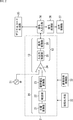
- FIG. 2 is a block diagram illustrating a configuration example of the pixel 2.
- the pixel 2 includes a photoelectric conversion unit 21, a transfer unit 22, a charge / voltage conversion unit 23, a comparator 24, an input / output control unit 25, and a signal storage unit 26.
- the photoelectric conversion unit 21, the transfer unit 22, and the charge-voltage conversion unit 23 constitute the pixel circuit 14 in FIG.
- the comparator 24, the input / output control unit 25, and the signal storage unit 26 constitute the ADC 13 of FIG. 1, and the comparator 24 corresponds to the comparison circuit 11, and the input / output control unit 25 and the signal storage unit. 26 corresponds to the data storage unit 12.
- the pixel 2 is connected to a reference signal generator 31 that generates a reference signal REF similar to the DAC 6 in FIG. Further, the pixel 2 includes an initialization unit 32 that initializes (resets) the photoelectric conversion unit 21, the charge-voltage conversion unit 23, and the comparator 24, and a conversion that controls switching of conversion efficiency in the charge-voltage conversion unit 23. An efficiency control unit 33 is connected.
- the signal storage unit 26 inputs and outputs a signal to and from the signal input / output unit 34 corresponding to the time code transfer unit 3 in FIG.
- the signal input / output unit 34 is supplied with a digital time code from the digital code generation unit 35 corresponding to the time code generation unit 7 of FIG. 1, and the signal output from the signal storage unit 26 to the signal input / output unit 34 is shown in FIG. 1 is output via a signal processing unit 36 and an output control unit 37 corresponding to one output unit 9.
- FIG. 2 shows a configuration example in which one ADC 13 is arranged for one pixel circuit 14, for example, for an area in which a predetermined number of pixel circuits 14 are arranged.
- a configuration in which one ADC 13 is arranged may be employed.
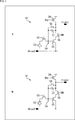
- FIG. 3A shows a circuit configuration of the pixel circuit 14 at the reference conversion efficiency which is the reference conversion efficiency
- FIG. 3B shows a high conversion having a conversion efficiency higher than the reference conversion efficiency.
- a circuit configuration of the pixel circuit 14 at the time of efficiency is shown.
- the pixel circuit 14 includes a PD (Photodiode) 52, a transfer transistor 53, an FD (Floating Diffusion) unit 54, an amplification transistor 55, an enable transistor 56, a capacitor 57, a changeover switch 58, and a transistor 59.
- PD 52 corresponds to the photoelectric conversion unit 21 in FIG. 2
- the transfer transistor 53 corresponds to the transfer unit 22 in FIG. 2
- the amplification transistor 55, the enable transistor 56, the capacitor 57, the changeover switch 58, and the transistor 59 include This corresponds to the charge-voltage converter 23 in FIG.
- the PD 52 receives light applied to the pixels 2 and performs photoelectric conversion, and generates and accumulates charges corresponding to the amount of light.
- the transfer transistor 53 has one of the source / drain connected to the PD 52 and the other source / drain connected to the FD unit 54, and charges generated in the PD 52 according to the transfer signal TG supplied to the gate electrode. Transfer to the FD unit 54.
- the FD portion 54 is a floating diffusion region that temporarily accumulates the charges transferred through the transfer transistor 53.
- one of the source / drain is connected to the enable transistor 56, and the other of the source / drain is connected to the bias voltage, and the charge accumulated in the FD portion 54 connected to the gate electrode.
- the enable transistor 56 has one of its source / drain connected to the output terminal PixOut and the other source / drain connected to the amplifying transistor 55, and is turned on according to an enable signal EN that controls whether the amplifying transistor 55 is valid or invalid. / Turn off.
- the capacitor 57 has one terminal connected to the FD unit 54 and the other terminal connected to the output terminal PixOut, thereby forming a feedback capacitor.
- the changeover switch 58 has one terminal connected to the FD unit 54 in parallel with the capacitor 57 and the other terminal connected to the output terminal PixOut.
- one of the source / drain is connected to the power supply voltage, and one of the source / drain is connected to the output terminal PixOut, and the bias voltage Vbp is supplied to the gate electrode.
- the conversion efficiency control unit 33 of FIG. Conversion efficiency can be switched between conversion efficiency and high conversion efficiency.
- the changeover switch 58 is controlled to be on during the reference conversion efficiency.
- the pixel circuit 14 has a circuit configuration in which source follower readout is performed, and an analog pixel signal in which charges are converted into voltage with reference conversion efficiency is output from the output terminal PixOut to the subsequent comparator 24 (see FIG. 4). Read out. That is, at this time, after the FD unit 54 is initialized and the ADC 13 acquires the pixel signal at the reset level, the bias of the transistor (PMOS) 59 also becomes a voltage at which the transistor 59 is turned off. During this time, the enable transistors 56 are also connected vertically, and are set to a low voltage so that the amplification transistor 55 directly connected to the FD unit 54 is disabled.
- PMOS transistor
- the changeover switch 58 is controlled to be off.
- the pixel circuit 14 has a circuit configuration in which source-grounded readout is performed, and an analog pixel signal in which charges are converted into voltage with high conversion efficiency is output from the output terminal PixOut to the subsequent comparator 24 (see FIG. 4).
- the transistor (PMOS) 59 is biased to have a constant current.
- the enable transistors 56 are connected vertically, and are set to a high voltage so that the amplification transistor 55 directly connected to the FD unit 54 operates as a source-grounded operational amplifier.
- the bias voltage VbiasS is determined to have an appropriate balance so as to be as low as possible from the viewpoint of the operating range of the output terminal PixOut so that it is as high as possible from the viewpoint of transferring pixel signals.
- the reset in the pixel circuit 14 can be performed by using the changeover switch 58, and the voltage immediately after the changeover switch 58 is turned off is read as the reset level. Thereafter, the signal level is transferred from the PD 52 to the FD unit 54 via the transfer transistor 53 and read.
- the pixel circuit 14 is configured to be able to switch the conversion efficiency when converting the charge generated in the PD 52 into a voltage.
- the pixel circuit 14 has a high conversion efficiency at low illuminance, thereby reducing noise at low illuminance. The characteristics can be improved.
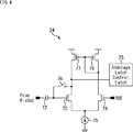
- FIG. 4 shows a circuit configuration of the comparator 24 that is the previous stage of the ADC 13.
- the comparator 24 includes a capacitor 72, transistors 73 and 74, a constant current source 75, an auto zero switch 76, and transistors 77 and 78.
- the capacitor 72 has one terminal connected to the output terminal (PixOut) of the pixel circuit 14 and the other terminal connected to the gate electrode of the transistor 73, so that the analog pixel signal output from the pixel circuit 14 Cut the DC component.
- the pixel signal output from the pixel circuit 14 is supplied to the transistor 73 via the capacitor 72.
- the reference signal REF is supplied to the transistor 74 from the reference signal generation unit 31 in FIG. 2, and the transistor 74 forms a differential pair with the amplification transistor 55 in FIG.
- the auto zero switch 76 is connected between the connection point of the capacitor 72 and the transistor 73 and the connection point of the transistor 73 and the transistor 77, and is used to align the operating points.
- Transistors 77 and 78 form a current mirror.
- An input / output control unit 25 that is a subsequent stage of the ADC 13 is connected between the transistor 73 and the transistor 77.
- the capacitor 72 can store the offset of the output of the pixel circuit 14 with auto-zero. If the circuit design of the comparator 24 makes it possible to align the operating points, the capacitor 72 and the auto zero switch 76 are unnecessary. However, from the viewpoint that the operating points vary, the capacitor 72 and the auto zero switch 76 are not required. A configuration having 76 is preferable.
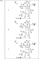
- FIG. 5A shows the circuit configuration of the pixel circuit 14A at the time of the reference conversion efficiency
- FIG. 5B shows the circuit configuration of the pixel circuit 14A at the time of the high conversion efficiency
- C shows the circuit configuration of the pixel circuit 14A when the conversion efficiency is low.
- the same reference numerals are given to the same components as those in the pixel circuit 14 shown in FIG. 3, and detailed description thereof is omitted.
- the pixel circuit 14 ⁇ / b> A includes a PD 52, a transfer transistor 53, an FD unit 54, an amplification transistor 55, an enable transistor 56, a capacitor 57, a changeover switch 58, and a transistor 59. 14 and in common.
- the pixel circuit 14A further includes a changeover switch 60 and a capacitor 61.
- the changeover switch 60 has one terminal connected to the FD unit 54 and the other terminal connected to the capacitor 61. Like the changeover switch 58, the changeover switch 60 is turned on / off by the conversion efficiency control unit 33 in FIG. Be controlled.
- the capacitor 61 has one terminal connected to the changeover switch 60 and the other terminal grounded.
- the pixel circuit 14A configured in this way can switch the conversion efficiency in three stages of reference conversion efficiency, high conversion efficiency, and low conversion efficiency.
- the pixel circuit 14A turns on the changeover switch 58 and turns off the changeover switch 60 so that the capacitor 61 is disconnected, that is, as shown in FIG.
- the circuit configuration is the same, and the reference conversion efficiency is set.
- the pixel circuit 14A has the same circuit configuration as that of FIG. 3B by setting both the changeover switch 58 and the changeover switch 60 to OFF, and is set to high conversion efficiency.
- the pixel circuit 14A is set to low conversion efficiency by connecting the capacitor 61 by turning on both the changeover switch 58 and the changeover switch 60.
- the pixel circuit 14A can realize three types of conversion efficiency by switching the connection of the capacitor 61 for reducing the conversion efficiency.
- FIG. 6 a description will be given of a circuit configuration of a pixel circuit 14B as a third configuration example and switching of conversion efficiency in the pixel circuit 14B.
- the same reference numerals are given to the same components as those in the pixel circuit 14 in FIG. 3 and the pixel circuit 14A in FIG. 5, and detailed description thereof is omitted.
- the pixel circuit 14B is common to the pixel circuit 14 of FIG. 3 in that it includes an FD unit 54, an amplification transistor 55, an enable transistor 56, a capacitor 57, a changeover switch 58, and a transistor 59. Furthermore, the pixel circuit 14B is common to the pixel circuit 14A of FIG. 5 in that it includes a changeover switch 60 and a capacitor 61.
- the pixel circuit 14B further includes PDs 52a and 52b, transfer transistors 53a and 53b, and discharge transistors 62a and 62b.
- the PD 52a and the PD 52b are formed to have different sensitivities, the sensitivity of the PD 52a is small, and the sensitivity of the PD 52b is large.
- the PD 52a and the PD 52b are different in sensitivity by changing the size as the light receiving area, the light receiving sensitivity (for example, the size of the on-chip microlens, the difference in the characteristics of the detection wavelength (color filter)), and the like. Can be set to
- the pixel circuit 14B controls the transfer transistors 53a and 53b and the discharge transistors 62a and 62b, and selects one of the PDs 52a and 52b to be used for image construction, thereby increasing the sensitivity to three levels. Can be switched. That is, it is possible to switch to using only the PD 52a having a low sensitivity, using only the PD 52b having a high sensitivity, or using both the PD 52a and the PD 52b.
- the PD 52b is continuously reset by the discharge transistor 62b different from the transfer transistor 53b.
- the PD 52a is continuously reset by the discharge transistor 62a different from the transfer transistor 53a.
- the transfer transistors 53a and 53b are driven simultaneously.
- the pixel circuit 14B can change the sensitivity in three stages, that is, only the PD 52a having a low sensitivity is used, only the PD 52b having a high sensitivity is used, or both the PD 52a and the PD 52b are added and used. .
- FIG. 7 illustrates processing performed in the solid-state imaging device 1 including the pixel circuit 14 illustrated in FIG.
- step S ⁇ b> 11 the solid-state imaging device 1 performs sensing on all the pixels 2 arranged in the pixel array unit 4, and each pixel 2 Charges corresponding to the amount of received light are generated.
- Step S12 the pixel 2 converts the charge into voltage with the conversion efficiency set at the present time, and outputs the AD converted pixel signal, and the conversion efficiency control unit 33 acquires the pixel signal.
- step S13 the conversion efficiency control unit 33 calculates a histogram of pixel signals of all the pixels 2. Then, for example, the conversion efficiency control unit 33 removes defects from the histograms of all the pixel signals, and compares the number of pixels of the saturated pixel signal with a predetermined threshold value.
- FIG. 8 shows an example of a histogram calculated by the conversion efficiency control unit 33.
- FIG. 8A shows a histogram when the number of pixels of a saturated pixel signal among the pixel signals output from all the pixels 2 is equal to or greater than a threshold value.
- the conversion efficiency control unit 33 acquires a comparison result that an image constructed by these pixel signals is too bright.
- FIG. 8B shows a histogram when the number of saturated pixel signals in the pixel signals output from all the pixels 2 is small.
- the conversion efficiency control unit 33 obtains the number of pixels of the pixel signal that saturates when the conversion efficiency set at the present time is switched to the high conversion efficiency. Then, even after switching to high conversion efficiency, if the level of the pixel signal is so small that the number of pixels of the saturated pixel signal does not exist, the conversion efficiency control unit 33 is too dark. Get the comparison result.
- step S14 the conversion efficiency control unit 33 determines whether to switch the conversion efficiency according to the comparison result in step S13. For example, the conversion efficiency control unit 33 determines to switch the conversion efficiency when the comparison result indicates that the image is too bright or the comparison result indicates that the image is too dark. On the other hand, the conversion efficiency control unit 33 determines that the conversion efficiency is not switched when the comparison result indicates that the image has appropriate brightness (that is, it is neither too bright nor too dark).
- step S14 If the conversion efficiency control unit 33 determines in step S14 that the conversion efficiency is not switched, that is, if it is a comparison result that the image has an appropriate brightness with the conversion efficiency set at the present time, the process proceeds to step S14. Return to S11. That is, in this case, the same processing is repeated with the conversion efficiency currently set as it is.
- step S14 determines in step S14 to switch the conversion efficiency
- step S15 the conversion efficiency control unit 33 controls the charge voltage conversion unit 23 to switch the conversion efficiency according to the comparison result in step S13, that is, according to the brightness of the image based on the pixel signal.
- the conversion efficiency control unit 33 determines the conversion efficiency when the number of pixels of the saturated pixel signal is equal to or greater than the threshold and the comparison result indicates that the image is too bright.
- the charge / voltage converter 23 is controlled so as to be lowered.
- the number of pixels of the saturated pixel signal becomes almost zero, and the solid-state imaging device 1 can acquire an image with appropriate brightness.
- the conversion efficiency control unit 33 has a low pixel signal level so that the number of pixels of the saturated pixel signal is small and there is no number of pixels of the saturated pixel signal even when switching to high conversion efficiency. If the comparison result indicates that the charge / voltage conversion unit 23 is too dark, the charge / voltage conversion unit 23 is controlled to increase the conversion efficiency. At this time, the conversion efficiency control unit 33 can switch the charge voltage conversion unit 23 to the high conversion efficiency for all the pixels 2 at the same time. As described above, the noise characteristics can be improved by making the charge-voltage conversion unit 23 have a high conversion efficiency, and the solid-state imaging device 1 has a low noise even when the illuminance is low so that an image usually becomes dark. Images can be acquired.
- step S15 After the process of step S15, the process returns to step S11, and the same process is repeated thereafter with the newly set conversion efficiency.
- the conversion efficiency control unit 33 can appropriately set the conversion efficiency of the charge-voltage conversion unit 23 according to the brightness of the image, and the solid-state imaging device 1 can display an image with appropriate brightness and less noise. Can be acquired.
- the control based on the threshold value can be performed to switch the conversion efficiency in three stages. it can.
- FIG. 9 illustrates processing performed in the solid-state imaging device 1 including the pixel circuit 14B illustrated in FIG.
- steps S21 to S23 processing similar to that in steps S11 to S13 in FIG. 7 is performed.
- step S23 comparison using the same histogram as shown in FIG. 8 is performed.
- step S24 the conversion efficiency control unit 33 determines whether to switch the PD 52 used for image construction.
- step S24 if the conversion efficiency control unit 33 determines not to switch the PD 52 used for image construction, the process returns to step S21. That is, in this case, of the PDs 52a and 52b shown in FIG. 6, the one currently used for image construction is continuously used, and the same processing is repeated thereafter.
- step S24 determines in step S24 to switch the PD 52 used for image construction.
- step S25 the conversion efficiency control unit 33 performs control to switch the PD 52 used for image construction according to the comparison result in step S13, that is, according to the brightness of the image based on the pixel signal.
- the conversion efficiency control unit 33 selects a PD 52a having a low sensitivity when a pixel signal of a certain level or more is output, as in the case of switching the conversion efficiency by controlling the changeover switches 58 and 60, and selects the PD 52a within a certain range.
- the highly sensitive PD 52b is selected, and when the pixel signal is the least, the PD 52a and 52b are both used to perform switching so as to obtain the maximum pixel signal.
- step S25 After the process of step S25, the process returns to step S21, and thereafter, the same process is repeated using the newly set PD 52.
- the conversion efficiency control unit 33 can switch the PD 52 to be used in accordance with the brightness of the image and appropriately set the sensitivity, and the solid-state imaging device 1 can select an image with more appropriate brightness and less noise. Can be acquired.
- FIG. 10 is a diagram illustrating an example of a detailed circuit configuration of the pixel 2.
- FIG. 10 shows a circuit configuration example of the pixel 2 that includes the pixel circuit 14A of FIG. 5 and can switch conversion efficiency in three stages.
- the pixel 2 is configured by including a bias circuit 81 between the pixel circuit 14A and the ADC 13, and the bias circuit 81 is configured by combining transistors 91 to 96.
- bias circuit 81 may be provided for each pixel circuit 14A, the bias circuit 81 may be shared by four pixel circuits 14A, or a larger number of bias circuits 81 may be provided.
- the pixel circuit 14A may supply the pixel circuit.
- the bias voltage ENPbias supplied to the gate electrode of the transistor 92, the source voltage of the transistor 93, and the drain voltage of the transistor 96 can be shared by all the bias circuits 81.
- the ADC 13 includes a comparator 24 (see FIG. 4), a band limiting unit 82, transistors 83 and 84, a positive feedback circuit (PFB) 85, an input / output control unit 25, and a signal storage unit 26.
- PFB positive feedback circuit
- the band limiting unit 82 includes a capacitor 101, and performs band limitation on the output signal output from the comparator 24.
- the output signal output from the comparator 24 and band-limited by the band-limiting unit 82 is once received by the transistor 83 and input to the positive feedback circuit 85 via the transistor 84 connected in series with the transistor 83. .
- the positive feedback circuit 85 is configured by combining transistors 111 to 117, and the transistors 114 to 117 constitute a NOR circuit.
- the positive feedback circuit 85 can speed up the response to the output signal output from the comparator 24 by feeding back the output to the input.
- the input / output control unit 25 is configured by combining an inverter 121, a NAND circuit 122, and an inverter 123.
- the signal storage unit 26 includes a plurality of 1-bit latches 131, and each latch 131 includes a switch 132 and inverters 133 and 134.
- FIG. 11 is a diagram illustrating an example of a detailed circuit configuration of the signal input / output unit 34.
- the signal input / output unit 34 includes a transistor 141, a tristate inverter 142, a tristate buffer 143, FF circuits 144-1 to 144-N, buffer circuits 145-1 to 145-N, and an FF circuit 146. -1 to 146-N and buffer circuits 147-1 to 147-N are connected.
- one set of FF circuits and buffer circuits are provided for each of the latches 131 included in the signal storage unit 26, and a plurality of sets are provided according to the number of bits required for the signal storage unit 26.
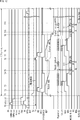
- FIG. 12 shows a drive waveform at the reference conversion efficiency at which the conversion efficiency is medium among the conversion efficiencies that can be switched in three stages in the pixel circuit 14A.
- FIG. 13 shows a drive waveform at the low conversion efficiency.
- FIG. 14 shows a drive waveform at a high conversion efficiency. Timings T0 to T11 that are common in FIGS. 12 to 14 will be described later, and timings a to d will be described first.
- the FD unit 54 ahead of the transfer transistor 53 keeps the reset signal RST supplied to the changeover switch 58 at “H”, so that the comparator 24 Conductive with the input side.
- the capacitance 57 which is the parasitic capacitance of this portion determines the conversion efficiency.
- the potential of the portion connected to the transistor (PMOS) 59 drops to almost GND because the conduction of the enable transistor 56 is cut off, whereby the charge-voltage converter 23 is initialized.
- the bias voltage Vb supplied to the transistor 96 becomes “L” in which no current flows.
- the control may be left as it is, or the transistor 93 is turned ON again at the timing c after the bias voltage Vb is set to “L” in order to set the potential of the differential amplifier to High. Also good.
- the capacitor Cgs of the common source amplifier is used. That is, when the bias voltage Vb is supplied to the transistor 96, a constant current flows, and the bias circuit 81 is activated.
- the reset signal RST supplied to the changeover switch 58 and the initialization signal Rini supplied to the transistor 96 are driven at the same time so that the initialization voltage Vrini is applied to the side of the transfer transistor 53 as in a differential circuit. Is set in the FD section 54 of Then, by slowly turning OFF the reset signal RST and the initialization signal Rini, the charge injection and the clock feedthrough can be made the same amount while the operating point is the initialization voltage Vrini.
- the input signal of the ADC 13 that follows has a relationship that the voltage at the reset level is low and the voltage at the signal level is high. Therefore, in this case, the signal input to the comparator 24 is not controlled with a high reset level as shown in FIGS. 12 and 13, and the voltage is set low. On the other hand, the signal level is controlled at a high potential as shown in FIGS. By controlling in this way, switching of three types of conversion efficiencies can be realized with the same pixel circuit 14A.
- timings T0 to T11 that are common to FIGS. 12 to 14 will be described.
- the PD 52 is initialized by an OFG signal supplied to a discharge transistor (not shown).
- An exposure (accumulation) period is from the timing when the OFG signal is switched from ON to OFF until the timing when the TG signal supplied to the transfer transistor 53 is switched from ON to OFF.
- the exposure (accumulation) period is from the timing when the TG signal is switched from ON to OFF one frame before the timing when the TG signal is switched from ON to OFF next time.
- the OFG signal is illustrated as a pulse with a short ON period, but the ON period may be long, or a plurality of pulses with two or more ON periods may be used. May be entered. Further, from the viewpoint of suppressing overflow, an intermediate voltage, an intermediate pulse, or the like may be used as the OFG signal instead of the binary values of ON and OFF.
- the potential of the REF signal supplied to the transistor 74 is set to be the initial voltage of the FD unit 54, and the FD unit 54 is initialized.
- the FD unit 54 can be soft reset (gradual transition from linear to saturation region to reduce kT / C noise to about 1/2).
- the FDG signal supplied to the changeover switch 60 is kept ON, and the same control is performed by the RST signal supplied to the changeover switch 58 so that the changeover switch 58 and the changeover switch 60 are connected. The conversion efficiency can be reduced by the capacity 57.
- the RST signal and the FDG signal are not fixed voltages and may be controlled simultaneously.
- the second floating portion of the comparator 24 is initialized by the INI signal supplied to the transistor 111 and the INI2 signal supplied to the transistor 112.
- the INI signal and the INI2 signal are described separately, but they may be the same signal.
- the FORCEVCO signal supplied to the transistors 115 and 117 the output of the comparator 24 is in a Ready state, and a signal can be written to the latch 131.
- a signal input / output unit 34 that inputs a time code generated by the time code generation unit 7 and outputs AD conversion pixel data that is a time code stored in the signal storage unit 26 is provided.
- the time code is written to the latch 131 from the outside by the WEN signal that is controlled and supplied to the tri-state buffer 143.
- a REF signal which is a monotonously decreasing slope signal, is input to the transistor 74, and the VCO signal is inverted at a timing inverted compared with the potential of the FD unit 54.
- the time code that has been continuously written is stored in the latch 131, and the writing operation to the corresponding latch 131 is stopped.
- the positive feedback circuit 85 which is a positive feedback circuit, is configured so that the VCO signal operates even when the current in the previous stage of the comparator 24 is several nA. Therefore, once the output of the previous stage of the comparator 24 is received by the transistor 83 of the second stage, a high PSRR (power supply voltage fluctuation removal ratio) can be realized. Subsequently, by connecting to the transistor 84, which is a high voltage NMOS, control is performed so that the voltage of the floating portion V2nd beyond that does not exceed the gate potential. This gate potential can use the same power supply as the logic circuit in the subsequent stage, but a different voltage may be used.
- a positive feedback is built in the floating part V2nd by a NOR circuit controlled by a test signal and a FORCEVCO signal as a malfunction prevention function, thereby enabling high-speed transition.
- the time code written in the latch 131 is fixed because the signal input / output unit 34 is constituted by a multi-stage connection of flip-flops as shown in FIG. It becomes an offset.
- the offset of the time code written in the latch 131 is canceled because the same offset is superimposed on the signal level by the CDS calculation.
- the comparator 24 that has not been inverted for some reason is forcibly inverted by the FORCEVCO signal, so that it is possible to avoid affecting the subsequent reading process.
- the reason for not inversion includes reasons such as a circuit failure or that the PD 52 is exposed to strong light and the potential is lower than the voltage at the end of the slope.
- the constant current of the comparator 24 can be made zero, and then the potential of the REF signal becomes high, It is possible to suppress power consumption until a constant current flows through the comparator 24.
- AD conversion pixel data (digital data) stored in the latch 131 is read out.
- the latch 131 is formed with a size close to the minimum dimension that can be processed for area reasons, so that the driving force of the NMOS and the PMOS is not balanced. Therefore, the read capability (time) differs depending on whether the signal inside the latch 131 is “H” or “L” and whether the read destination LBL (Local Bit Line) is “H” or “L”. turn into.
- the signal of the latch 131 may change when the signal of the latch 131 is read depending on the impedance of the LBL. In order to prevent such a concern, control is devised so that the impedance of the transistor 141 controlled by the xPC signal and the external impedance of the latch 131 when reading the latch signal are high when viewed from the latch 131.
- the NMOS since the transistor has a higher mutual conductance gm than the PMOS, the NMOS is lower than the PMOS. Therefore, the method of lowering the LBL “H” to “L” by the NMOS rather than pulling the LBL “L” to “H” by the PMOS. Works fast. For this reason, before reading by the xPC signal, the power supply is once set, and LBL is preset to “H” every time. The read from the latch 131 is not different from the preset value when the read signal is “H”, so it is not affected even if the capacity of the PMOS is low, and the PMOS has a low driving power. May be.
- the NMOS is responsible for lowering the potential of the LBL precharged to “H”.
- the gate width W is usually increased, but this increases the area cost.
- the impedance of the LBL viewed from the inverters 133 and 134 inside the latch 131 is improved. Specifically, with respect to the switch 132 provided at the output of the latch 131, at the time of writing, both the NMOS and the PMOS constituting the latch 131 are turned on, while at the time of reading, only the NMOS is turned on. Take control. This makes it possible to read signals at high speed and robustly without increasing the size of many NMOS transistors in the latch 131.
- the signal read to the LBL is read to the flip-flop with the AD conversion clock set to L with the REN signal ON, and the signal is output to the output by inputting the AD conversion clock after the REN signal is OFF. Is transferred to the bucket relay system.
- data is temporarily written in a memory such as SRAM (Static Random Access Memory) (not shown) provided in the solid-state imaging device 1 once.
- SRAM Static Random Access Memory
- the voltage of the REF signal is returned to a high level, the TG signal supplied to the transfer transistor 53 is turned on, and the charge of the PD 52 is transferred to the FD unit 54.
- timing T10 From timing T7 to timing T10, processing similar to that from timing T2 to timing T5 is performed, and signal level AD conversion is performed.
- the reset level is read from the SRAM once stored and subtracted from the signal level. Accordingly, a series of circuit noises including the fixed pattern noise of the comparator 24 and the signal input / output unit 34 and the random noise of the pixel 2 and the comparator 24 can be canceled (correlated double sampling).
- a process of transmitting to the outside of the solid-state imaging device 1 is performed via a signal readout circuit, for example, via a high-speed serial interface such as SLVS-EC (Scalable Voltage Signaling with Embedded Clock). Note that a process of narrowing the data band such as signal compression may be performed before this process.
- SLVS-EC Scalable Voltage Signaling with Embedded Clock
- the pixel 2 is driven by the control method as described above, and the noise and speed of the output signal can be reduced.
- the signal storage unit 26 stores both a reset level code and a light reception signal level code, and outputs the codes to the outside of the solid-state imaging device 1 sequentially or simultaneously by two or more plural repeaters. Can be adopted.
- the solid-state imaging device 1 including the comparison circuit 11 a stacked structure in which two or three semiconductor wafers are stacked, or a stacked structure in which more than that is stacked may be employed.
- the code transition by the AD conversion clock is made finer at low illuminance while the slope of the REF signal is constant, and the code transition becomes coarser at high illuminance. By controlling in this way, it is also possible to improve the power efficiency by reducing the number of circuit transitions.
- control signal when the control signal becomes insufficient in the solid-state imaging device 1 due to multi-pixels and multi-circuits, the drive capability of the signal is appropriately improved such as buffering, and the category of the design act.
- the circuit may be changed.
- the solid-state imaging device 1 as described above is applied to various electronic devices such as an imaging system such as a digital still camera and a digital video camera, a mobile phone having an imaging function, or other devices having an imaging function. be able to.
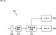
- FIG. 15 is a block diagram illustrating a configuration example of an imaging device mounted on an electronic device.
- the imaging apparatus 201 includes an optical system 202, an imaging element 203, a signal processing circuit 204, a monitor 205, and a memory 206, and can capture still images and moving images.
- the optical system 202 includes one or more lenses, guides image light (incident light) from a subject to the image sensor 203, and forms an image on a light receiving surface (sensor unit) of the image sensor 203.
- the solid-state imaging device 1 described above is applied as the imaging element 203.
- the image sensor 203 electrons are accumulated for a certain period according to the image formed on the light receiving surface via the optical system 202. Then, a signal corresponding to the electrons accumulated in the image sensor 203 is supplied to the signal processing circuit 204.
- the signal processing circuit 204 performs various signal processing on the pixel signal output from the image sensor 203.
- An image (image data) obtained by performing signal processing by the signal processing circuit 204 is supplied to the monitor 205 and displayed, or supplied to the memory 206 and stored (recorded).
- the imaging apparatus 201 configured as described above, by applying the solid-state imaging apparatus 1 described above, for example, an image with little noise can be captured even at low illuminance.
- FIG. 16 is a diagram illustrating a usage example in which the above-described image sensor (solid-state imaging device) is used.
- the image sensor described above can be used in various cases for sensing light such as visible light, infrared light, ultraviolet light, and X-ray as follows.
- Devices for taking images for viewing such as digital cameras and mobile devices with camera functions
- Devices used for traffic such as in-vehicle sensors that capture the back, surroundings, and interiors of vehicles, surveillance cameras that monitor traveling vehicles and roads, and ranging sensors that measure distances between vehicles, etc.
- Equipment used for home appliances such as TVs, refrigerators, air conditioners, etc. to take pictures and operate the equipment according to the gestures ⁇ Endoscopes, equipment that performs blood vessel photography by receiving infrared light, etc.
- Equipment used for medical and health care ⁇ Security equipment such as security surveillance cameras and personal authentication cameras ⁇ Skin measuring instrument for photographing skin and scalp photography Such as a microscope to do beauty Equipment used for sports-Equipment used for sports such as action cameras and wearable cameras for sports applications-Used for agriculture such as cameras for monitoring the condition of fields and crops apparatus
- the technology according to the present disclosure can be applied to various products.
- the technology according to the present disclosure is realized as a device that is mounted on any type of moving body such as an automobile, an electric vehicle, a hybrid electric vehicle, a motorcycle, a bicycle, personal mobility, an airplane, a drone, a ship, and a robot. May be.
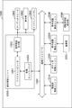
- FIG. 17 is a block diagram illustrating a schematic configuration example of a vehicle control system that is an example of a mobile control system to which the technology according to the present disclosure can be applied.
- the vehicle control system 12000 includes a plurality of electronic control units connected via a communication network 12001.
- the vehicle control system 12000 includes a drive system control unit 12010, a body system control unit 12020, a vehicle exterior information detection unit 12030, a vehicle interior information detection unit 12040, and an integrated control unit 12050.
- a microcomputer 12051, an audio image output unit 12052, and an in-vehicle network I / F (interface) 12053 are illustrated.
- the drive system control unit 12010 controls the operation of the device related to the drive system of the vehicle according to various programs.
- the drive system control unit 12010 includes a driving force generator for generating a driving force of a vehicle such as an internal combustion engine or a driving motor, a driving force transmission mechanism for transmitting the driving force to wheels, and a steering angle of the vehicle. It functions as a control device such as a steering mechanism that adjusts and a braking device that generates a braking force of the vehicle.
- the body system control unit 12020 controls the operation of various devices mounted on the vehicle body according to various programs.
- the body system control unit 12020 functions as a keyless entry system, a smart key system, a power window device, or a control device for various lamps such as a headlamp, a back lamp, a brake lamp, a blinker, or a fog lamp.
- the body control unit 12020 can be input with radio waves transmitted from a portable device that substitutes for a key or signals from various switches.
- the body system control unit 12020 receives input of these radio waves or signals, and controls a door lock device, a power window device, a lamp, and the like of the vehicle.
- the vehicle outside information detection unit 12030 detects information outside the vehicle on which the vehicle control system 12000 is mounted.
- the imaging unit 12031 is connected to the vehicle exterior information detection unit 12030.
- the vehicle exterior information detection unit 12030 causes the imaging unit 12031 to capture an image outside the vehicle and receives the captured image.
- the vehicle outside information detection unit 12030 may perform an object detection process or a distance detection process such as a person, a car, an obstacle, a sign, or a character on a road surface based on the received image.
- the imaging unit 12031 is an optical sensor that receives light and outputs an electrical signal corresponding to the amount of received light.
- the imaging unit 12031 can output an electrical signal as an image, or can output it as distance measurement information. Further, the light received by the imaging unit 12031 may be visible light or invisible light such as infrared rays.
- the vehicle interior information detection unit 12040 detects vehicle interior information.
- a driver state detection unit 12041 that detects a driver's state is connected to the in-vehicle information detection unit 12040.
- the driver state detection unit 12041 includes, for example, a camera that images the driver, and the vehicle interior information detection unit 12040 determines the degree of fatigue or concentration of the driver based on the detection information input from the driver state detection unit 12041. It may be calculated or it may be determined whether the driver is asleep.
- the microcomputer 12051 calculates a control target value of the driving force generator, the steering mechanism, or the braking device based on the information inside / outside the vehicle acquired by the vehicle outside information detection unit 12030 or the vehicle interior information detection unit 12040, and the drive system control unit A control command can be output to 12010.
- the microcomputer 12051 realizes an ADAS (Advanced Driver Assistance System) function including vehicle collision avoidance or impact mitigation, following traveling based on inter-vehicle distance, vehicle speed maintaining traveling, vehicle collision warning, or vehicle lane departure warning, etc. It is possible to perform cooperative control for the purpose.
- ADAS Advanced Driver Assistance System
- the microcomputer 12051 controls the driving force generator, the steering mechanism, the braking device, and the like based on the information around the vehicle acquired by the vehicle exterior information detection unit 12030 or the vehicle interior information detection unit 12040. It is possible to perform cooperative control for the purpose of automatic driving that autonomously travels without depending on the operation.
- the microcomputer 12051 can output a control command to the body system control unit 12020 based on information outside the vehicle acquired by the vehicle outside information detection unit 12030.
- the microcomputer 12051 controls the headlamp according to the position of the preceding vehicle or the oncoming vehicle detected by the vehicle outside information detection unit 12030, and performs cooperative control for the purpose of preventing glare such as switching from a high beam to a low beam. It can be carried out.
- the sound image output unit 12052 transmits an output signal of at least one of sound and image to an output device capable of visually or audibly notifying information to a vehicle occupant or the outside of the vehicle.
- an audio speaker 12061, a display unit 12062, and an instrument panel 12063 are illustrated as output devices.
- the display unit 12062 may include at least one of an on-board display and a head-up display, for example.
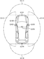
- FIG. 18 is a diagram illustrating an example of an installation position of the imaging unit 12031.
- the vehicle 12100 includes imaging units 12101, 12102, 12103, 12104, and 12105 as the imaging unit 12031.
- the imaging units 12101, 12102, 12103, 12104, and 12105 are provided, for example, at positions such as a front nose, a side mirror, a rear bumper, a back door, and an upper part of a windshield in the vehicle interior of the vehicle 12100.
- the imaging unit 12101 provided in the front nose and the imaging unit 12105 provided in the upper part of the windshield in the vehicle interior mainly acquire an image in front of the vehicle 12100.
- the imaging units 12102 and 12103 provided in the side mirror mainly acquire an image of the side of the vehicle 12100.
- the imaging unit 12104 provided in the rear bumper or the back door mainly acquires an image behind the vehicle 12100.
- the forward images acquired by the imaging units 12101 and 12105 are mainly used for detecting a preceding vehicle or a pedestrian, an obstacle, a traffic light, a traffic sign, a lane, or the like.
- FIG. 18 shows an example of the shooting range of the imaging units 12101 to 12104.
- the imaging range 12111 indicates the imaging range of the imaging unit 12101 provided in the front nose
- the imaging ranges 12112 and 12113 indicate the imaging ranges of the imaging units 12102 and 12103 provided in the side mirrors, respectively
- the imaging range 12114 The imaging range of the imaging part 12104 provided in the rear bumper or the back door is shown. For example, by superimposing the image data captured by the imaging units 12101 to 12104, an overhead image when the vehicle 12100 is viewed from above is obtained.
- At least one of the imaging units 12101 to 12104 may have a function of acquiring distance information.
- at least one of the imaging units 12101 to 12104 may be a stereo camera including a plurality of imaging elements, or may be an imaging element having pixels for phase difference detection.
- the microcomputer 12051 based on the distance information obtained from the imaging units 12101 to 12104, the distance to each three-dimensional object in the imaging range 12111 to 12114 and the temporal change of this distance (relative speed with respect to the vehicle 12100).
- a predetermined speed for example, 0 km / h or more
- the microcomputer 12051 can set an inter-vehicle distance to be secured in advance before the preceding vehicle, and can perform automatic brake control (including follow-up stop control), automatic acceleration control (including follow-up start control), and the like.
- automatic brake control including follow-up stop control
- automatic acceleration control including follow-up start control
- cooperative control for the purpose of autonomous driving or the like autonomously traveling without depending on the operation of the driver can be performed.
- the microcomputer 12051 converts the three-dimensional object data related to the three-dimensional object to other three-dimensional objects such as a two-wheeled vehicle, a normal vehicle, a large vehicle, a pedestrian, and a utility pole based on the distance information obtained from the imaging units 12101 to 12104. It can be classified and extracted and used for automatic avoidance of obstacles.
- the microcomputer 12051 identifies obstacles around the vehicle 12100 as obstacles that are visible to the driver of the vehicle 12100 and obstacles that are difficult to see.
- the microcomputer 12051 determines the collision risk indicating the risk of collision with each obstacle, and when the collision risk is equal to or higher than the set value and there is a possibility of collision, the microcomputer 12051 is connected via the audio speaker 12061 or the display unit 12062. By outputting an alarm to the driver and performing forced deceleration or avoidance steering via the drive system control unit 12010, driving assistance for collision avoidance can be performed.
- At least one of the imaging units 12101 to 12104 may be an infrared camera that detects infrared rays.
- the microcomputer 12051 can recognize a pedestrian by determining whether a pedestrian is present in the captured images of the imaging units 12101 to 12104.
- pedestrian recognition is, for example, whether or not a person is a pedestrian by performing a pattern matching process on a sequence of feature points indicating the outline of an object and a procedure for extracting feature points in the captured images of the imaging units 12101 to 12104 as infrared cameras. It is carried out by the procedure for determining.
- the audio image output unit 12052 When the microcomputer 12051 determines that a pedestrian is present in the captured images of the imaging units 12101 to 12104 and recognizes the pedestrian, the audio image output unit 12052 has a rectangular outline for emphasizing the recognized pedestrian.
- the display unit 12062 is controlled so as to be superimposed and displayed. Further, the audio image output unit 12052 may control the display unit 12062 so as to display an icon or the like indicating a pedestrian at a desired position.
- the technology according to the present disclosure may be applied to, for example, the imaging unit 12031 among the configurations described above.
- the technology according to the present disclosure may be applied to, for example, the imaging unit 12031 among the configurations described above.
- the technology according to the present disclosure to the imaging unit 12031 and the like, it is possible to obtain a captured image with lower noise and higher image quality.
- image recognition processing using the captured image can be performed with high accuracy. .
- a pixel circuit that outputs an analog pixel signal;
- a pixel having a digital conversion circuit that is arranged for each one of the pixel circuits or for each area where a predetermined number of the pixel circuits are arranged, and that digitally converts the pixel signals;
- the pixel circuit includes: A photoelectric conversion unit that receives light applied to the pixel, performs photoelectric conversion, and generates charges according to the amount of light; and A charge-voltage conversion unit capable of switching a conversion efficiency when converting the charge generated in the photoelectric conversion unit into a voltage between a reference conversion efficiency serving as a reference and a high conversion efficiency higher than the reference conversion efficiency element.
- the control unit according to (1) further including a control unit that acquires the pixel signal output from the pixel and controls switching of the conversion efficiency in the charge-voltage conversion unit according to image brightness based on the pixel signal.
- Image sensor (3) The image sensor according to (2), wherein when the image is darker than a predetermined threshold, the control unit switches the photoelectric conversion unit to a high conversion efficiency simultaneously for all the pixels.
- the charge-voltage conversion unit has a changeover switch for switching between a circuit configuration serving as a source follower readout realizing the reference conversion efficiency and a circuit configuration serving as a source grounded readout realizing the high conversion efficiency,
- the image pickup device according to (2) or (3) wherein the control unit controls the changeover switch.
- the charge-voltage conversion unit can switch the conversion efficiency in three stages of the reference conversion efficiency, the high conversion efficiency, and the low conversion efficiency lower than the reference conversion efficiency.
- a control unit that acquires the pixel signal output from the digital conversion circuit and switches a photoelectric conversion unit used to construct the image among a plurality of the photoelectric conversion units according to the brightness of the image based on the pixel signal.
- the imaging device further comprising: (8) The image sensor according to (7), wherein the pixel circuit includes, as the plurality of photoelectric conversion units, a first photoelectric conversion unit having a large light receiving area and a second photoelectric conversion unit having a small light receiving area. (9) The control unit switches use of the first photoelectric conversion unit, use of the second photoelectric conversion unit, or use of both the first photoelectric conversion unit and the second photoelectric conversion unit.
- the imaging device according to (8).
- a control unit that performs control in the image sensor A pixel circuit that outputs an analog pixel signal; and a digital conversion circuit that is disposed for each of the pixel circuits or for each area where a predetermined number of the pixel circuits are disposed, and that digitally converts the pixel signals.
- the photoelectric conversion unit that receives the light irradiated to the pixel and performs photoelectric conversion in the pixel circuit converts the electric charge generated according to the amount of light into a voltage.
- a control method including controlling the switching of the conversion efficiency in a charge-voltage conversion unit capable of switching the conversion efficiency between a reference conversion efficiency as a reference and a high conversion efficiency higher than the reference conversion efficiency.
- a pixel circuit that outputs an analog pixel signal;
- a pixel having a digital conversion circuit that is arranged for each one of the pixel circuits or for each area where a predetermined number of the pixel circuits are arranged, and that digitally converts the pixel signal;
- the pixel circuit includes: A photoelectric conversion unit that receives light applied to the pixel, performs photoelectric conversion, and generates charges according to the amount of light; and A charge-voltage conversion unit capable of switching a conversion efficiency when converting the charge generated in the photoelectric conversion unit into a voltage between a reference conversion efficiency serving as a reference and a high conversion efficiency higher than the reference conversion efficiency An electronic device provided with an element.
- 1 solid-state imaging device 2 pixels, 3 time code transfer unit, 4 pixel array unit, 5 pixel drive circuit, 6 DAC, 7 time code generation unit, 8 vertical drive circuit, 9 output unit, 10 timing generation circuit, 11 comparison circuit , 12 data storage unit, 13 ADC, 14 pixel circuit, 21 photoelectric conversion unit, 22 transfer unit, 23 charge voltage conversion unit, 24 comparator, 25 input / output control unit, 26 signal storage unit, 31 reference signal generation unit, 32 Initialization means, 33 conversion efficiency control section, 34 signal input / output section, 35 digital code generation section, 36 signal processing section, 37 output control section
Landscapes
- Engineering & Computer Science (AREA)
- Multimedia (AREA)
- Signal Processing (AREA)
- Transforming Light Signals Into Electric Signals (AREA)
- Solid State Image Pick-Up Elements (AREA)
Abstract
本開示は、低照度におけるノイズ特性を改善することができるようにする撮像素子、制御方法、および電子機器に関する。 画素は、アナログの画素信号を出力する画素回路と、画素信号をデジタル変換するデジタル変換回路とを有する。そして、画素回路は、画素に照射される光を受光して光電変換を行い、その光の光量に応じた電荷を発生する光電変換部と、光電変換部で発生した電荷を電圧に変換する際の変換効率を、基準となる基準変換効率と、前記基準変換効率よりも高い高変換効率とで切り替え可能な電荷電圧変換部とを有する。本技術は、例えば、画素内でAD変換を行う固体撮像装置に適用できる。
Description
本開示は、撮像素子、制御方法、および電子機器に関し、特に、低照度におけるノイズ特性を改善することができるようにした撮像素子、制御方法、および電子機器に関する。
近年、1画素ごとに1つのAD(Analog to Digital)変換器を有し、画素ごとに並列的に画素信号をAD変換する構成の固体撮像素子が開発されている。また、固体撮像素子は、1画素ごとではなく、複数の画素ごとにAD変換器を有し、それらの画素が配置されているエリアごとにAD変換するような構成を採用してもよい。
また、特許文献1には、1画素ごと、または、複数の画素ごとに設けられるAD変換器における変換効率を切り替え可能とし、変換効率を低くすることで高照度側の信号を取得して広ダイナミックレンジを実現することができる固体撮像装置が開示されている。
しかしながら、上述した特許文献1で開示されている固体撮像素子は、低照度側の信号に対する特段の対処について考慮されていない構成であった。そのため、AD変換器のノイズが、低照度におけるノイズ特性に与える影響が大きく、そのノイズ特性の改善が求められていた。
本開示は、このような状況に鑑みてなされたものであり、低照度におけるノイズ特性を改善することができるようにするものである。
本開示の一側面の撮像素子は、アナログの画素信号を出力する画素回路と、1個の前記画素回路ごと、または、所定個数の前記画素回路が配置されるエリアごとに配置され、前記画素信号をデジタル変換するデジタル変換回路とを有する画素を備え、前記画素回路は、前記画素に照射される光を受光して光電変換を行い、その光の光量に応じた電荷を発生する光電変換部と、前記光電変換部で発生した電荷を電圧に変換する際の変換効率を、基準となる基準変換効率と、前記基準変換効率よりも高い高変換効率とで切り替え可能な電荷電圧変換部とを有する。
本開示の一側面の制御方法は、撮像素子における制御を行う制御部が、アナログの画素信号を出力する画素回路と、1個の前記画素回路ごと、または、所定個数の前記画素回路が配置されるエリアごとに配置され、前記画素信号をデジタル変換するデジタル変換回路とを有する画素から出力される前記画素信号を取得することと、前記画素信号に基づく画像の明るさに従って、前記画素回路が有する、前記画素に照射される光を受光して光電変換を行う光電変換部において光の光量に応じて発生した電荷を電圧に変換する際の変換効率を、基準となる基準変換効率と、前記基準変換効率よりも高い高変換効率とで切り替え可能な電荷電圧変換部における前記変換効率の切り替えを制御することを含む。
本開示の一側面の電子機器は、アナログの画素信号を出力する画素回路と、1個の前記画素回路ごと、または、所定個数の前記画素回路が配置されるエリアごとに配置され、前記画素信号をデジタル変換するデジタル変換回路とを有する画素を有し、前記画素回路は、前記画素に照射される光を受光して光電変換を行い、その光の光量に応じた電荷を発生する光電変換部と、前記光電変換部で発生した電荷を電圧に変換する際の変換効率を、基準となる基準変換効率と、前記基準変換効率よりも高い高変換効率とで切り替え可能な電荷電圧変換部とを有する撮像素子を備える。
本開示の一側面においては、画素回路からアナログの画素信号が出力され、1個の画素回路ごと、または、所定個数の画素回路が配置されるエリアごとに配置されるデジタル変換回路により画素信号がデジタル変換される。また、光電変換部では、画素に照射される光を受光して光電変換が行われて、その光の光量に応じた電荷が発生し、電荷電圧変換部では、光電変換部で発生した電荷を電圧に変換する際の変換効率を、基準となる基準変換効率と、基準変換効率よりも高い高変換効率とで切り替え可能とされる。さらに、画素から出力される画素信号が取得され、その画素信号に基づく画像の明るさに従って、電荷電圧変換部における変換効率の切り替えが制御される。
本開示の一側面によれば、低照度におけるノイズ特性を改善することができる。
なお、ここに記載された効果は必ずしも限定されるものではなく、本開示中に記載されたいずれかの効果であってもよい。
以下、本技術を適用した具体的な実施の形態について、図面を参照しながら詳細に説明する。
<固体撮像装置の構成例>
図1は、本技術を適用した固体撮像装置の一実施の形態の構成例を示すブロック図である。
図1は、本技術を適用した固体撮像装置の一実施の形態の構成例を示すブロック図である。
図1に示すように、固体撮像装置1は、例えば、シリコン(Si)などの半導体を用いた半導体基板に、2次元アレイ状に複数の画素2が配列された画素アレイ部4を有する。さらに、画素アレイ部4には、時刻コード発生部7で生成された時刻コードを各画素2に転送する時刻コード転送部3も設けられている。また、固体撮像装置1は、画素アレイ部4の周辺に、画素駆動回路5、DAC(D/A Converter)6、時刻コード発生部7、垂直駆動回路8、出力部9、およびタイミング生成回路10が形成されている。
2次元アレイ状に配列された複数の画素2それぞれには、図1の右上に示すように、比較回路11およびデータ記憶部12を有するADC13と、受光素子(例えば、後述する図3のPD52)を有する画素回路14とが設けられている。例えば、画素2は、受光素子が受光した光量に応じた電荷信号が画素回路14から出力され、その電荷信号をADC13によって、アナログである画素信号SIGからデジタルの画素信号SIGに変換して出力する。
画素駆動回路5は、画素2内の画素回路14を駆動する。DAC6は、時間経過に応じてレベル(電圧)が単調減少するスロープ信号である参照信号(基準電圧信号)REFを生成し、各画素2に供給する。
時刻コード発生部7は、各画素2が、アナログの画素信号SIGをデジタルの信号に変換(AD変換)する際に使用される時刻コードを生成し、対応する時刻コード転送部3に供給する。時刻コード発生部7は、画素アレイ部4に対して複数個設けられており、画素アレイ部4内には、時刻コード発生部7に対応する数だけ、時刻コード転送部3が設けられている。即ち、時刻コード発生部7と、そこで生成された時刻コードを転送する時刻コード転送部3は、1対1に対応する。
垂直駆動回路8は、画素2内で生成されたデジタルの画素信号SIGを、タイミング生成回路10から供給されるタイミング信号に基づいて、所定の順番で出力部9に出力させる制御を行う。画素2から出力されたデジタルの画素信号SIGは、出力部9から固体撮像装置1の外部へ出力される。出力部9は、黒レベルを補正する黒レベル補正処理やCDS(Correlated Double Sampling;相関2重サンプリング)処理など、所定のデジタル信号処理を必要に応じて行い、その後、外部へ出力する。
タイミング生成回路10は、各種のタイミング信号を生成するタイミングジェネレータなどによって構成され、生成した各種のタイミング信号を、画素駆動回路5、DAC6、垂直駆動回路8などに供給する。
固体撮像装置1は、以上のように構成されている。なお、図1では、上述したように、固体撮像装置1を構成する全ての回路が、1つの半導体基板上に形成されるように説明したが、例えば、固体撮像装置1を構成する回路を複数枚の半導体基板に分けて配置する構成とすることもできる。
ここで、画素2の動作について説明する。
画素2では、受光素子が受光した光量に応じた電荷信号が、アナログの画素信号SIGとして画素回路14からADC13に出力され、ADC13においてデジタルの画素信号SIGにAD変換されて出力される。
ADC13では、比較回路11が、DAC6から供給される参照信号REFと画素信号SIGを比較し、比較結果を表す比較結果信号として出力信号VCOを出力する。例えば、比較回路11は、参照信号REFと画素信号SIGが同一(の電圧)になったとき、出力信号VCOを反転させる。
データ記憶部12には、比較回路11から出力信号VCOが入力される他、垂直駆動回路8から、画素信号の書き込み動作であることを表すWR信号(以下では、書き込み制御信号WRともいう)、画素信号の読み出し動作であることを表すRD信号(以下では、読み出し制御信号RDともいう)、および、画素信号の読み出し動作中における画素2の読み出しタイミングを制御するWORD信号が供給される。また、データ記憶部12には、時刻コード転送部3を介して、時刻コード発生部7で生成された時刻コードも供給される。なお、ここでは、画素2の動作を分かり易くするために、垂直駆動回路8が制御信号を生成して画素アレイ部4へ供給すると説明しているが、全画素同時に駆動する制御信号を生成する回路(図示せず)が、例えば、水平部分に配置される構成としてもよい。即ち、制御信号が画素アレイ部4へ供給される構成であれば、制御信号を生成する回路の配置が制約されることはない。
例えば、データ記憶部12は、WR信号及びRD信号に基づいて、時刻コードの書き込み動作と読み出し動作を制御するラッチ制御回路(例えば、後述する図2の入出力制御部25)と、時刻コードを記憶するラッチ記憶部(例えば、後述する図2の信号記憶部26)で構成される。
ラッチ制御回路は、時刻コードの書き込み動作においては、比較回路11からHi(High)の出力信号VCOが入力されている間、時刻コード転送部3から供給される、単位時間ごとに更新される時刻コードをラッチ記憶部に記憶させる。そして、参照信号REFと画素信号SIGが同一(の電圧)になり、比較回路11から供給される出力信号VCOがLo(Low)に反転されたとき、供給される時刻コードの書き込み(更新)を中止し、最後にラッチ記憶部に記憶された時刻コードをラッチ記憶部に保持させる。ラッチ記憶部に記憶された時刻コードは、画素信号SIGと参照信号REFが等しくなった時刻を表しており、画素信号SIGがその時刻の基準電圧であったことを示すデータ、即ち、デジタル化された光量値を表す。
参照信号REFの掃引が終了し、画素アレイ部4内の全ての画素2のラッチ記憶部に時刻コードが記憶された後、画素2の動作が、書き込み動作から読み出し動作に変更される。
ラッチ制御回路は、時刻コードの読み出し動作においては、読み出しタイミングを制御するWORD信号に基づいて、画素2が自分の読み出しタイミングとなったときに、ラッチ記憶部に記憶されている時刻コード(デジタルの画素信号SIG)を、時刻コード転送部3に出力する。時刻コード転送部3は、供給された時刻コードを、列方向(垂直方向)に順次転送し、出力部9に供給する。
以下では、時刻コードの書き込み動作においてラッチ記憶部に書き込まれる時刻コードと区別するため、時刻コードの読み出し動作においてラッチ記憶部から読み出される出力信号VCOが反転したときの反転時刻コードである、画素信号SIGがその時刻の基準電圧であったことを示すデジタル化された画素データを、AD変換画素データとも称する。
<画素の構成例>
図2は、画素2の構成例を示すブロック図である。
図2は、画素2の構成例を示すブロック図である。
図2に示すように、画素2は、光電変換部21、転送部22、電荷電圧変換部23、比較器24、入出力制御部25、および信号記憶部26により構成される。例えば、光電変換部21、転送部22、および電荷電圧変換部23は、図1の画素回路14を構成する。同様に、比較器24、入出力制御部25、および信号記憶部26は、図1のADC13を構成しており、比較器24が比較回路11に対応し、入出力制御部25および信号記憶部26がデータ記憶部12に対応する。
また、画素2には、図1のDAC6と同様の参照信号REFを発生する参照信号発生部31が接続されている。さらに、画素2には、光電変換部21、電荷電圧変換部23、および比較器24を初期化(リセット)する初期化手段32、並びに、電荷電圧変換部23における変換効率の切り替えを制御する変換効率制御部33が接続されている。
また、信号記憶部26は、図1の時刻コード転送部3に対応する信号入出力部34との間で信号を入出力する。信号入出力部34は、図1の時刻コード発生部7に対応するデジタルコード生成部35からデジタルの時刻コードが供給され、信号記憶部26から信号入出力部34に出力された信号は、図1の出力部9に対応する信号処理部36および出力制御部37を介して出力される。
なお、図2の画素2では、1個の画素回路14に対して1個のADC13が配置される構成例が示されているが、例えば、所定個数の画素回路14が配置されるエリアに対して1個のADC13が配置されるような構成を採用してもよい。
<画素回路の第1の構成例>
図3を参照して、第1の構成例となる画素回路14の回路構成、および、画素回路14での変換効率の切り替えについて説明する。
図3を参照して、第1の構成例となる画素回路14の回路構成、および、画素回路14での変換効率の切り替えについて説明する。
図3のAには、基準となる変換効率である基準変換効率時における画素回路14の回路構成が示されており、図3のBには、基準変換効率よりも高い変換効率である高変換効率時における画素回路14の回路構成が示されている。
図3に示すように、画素回路14は、PD(Photodiode)52、転送トランジスタ53、FD(Floating Diffusion)部54、増幅トランジスタ55、イネーブルトランジスタ56、容量57、切り替えスイッチ58、およびトランジスタ59を備えて構成される。例えば、PD52は、図2の光電変換部21に対応し、転送トランジスタ53は、図2の転送部22に対応し、増幅トランジスタ55、イネーブルトランジスタ56、容量57、切り替えスイッチ58、およびトランジスタ59は、図2の電荷電圧変換部23に対応する。
PD52は、画素2に照射される光を受光して光電変換を行い、その光の光量に応じた電荷を発生して蓄積する。
転送トランジスタ53は、ソース/ドレインの一方がPD52に接続されるとともに、ソース/ドレインの他方がFD部54に接続されており、ゲート電極に供給される転送信号TGに従って、PD52で発生した電荷をFD部54に転送する。
FD部54は、転送トランジスタ53を介して転送されてくる電荷を一時的に蓄積する浮遊拡散領域である。
増幅トランジスタ55は、ソース/ドレインの一方がイネーブルトランジスタ56に接続されるとともに、ソース/ドレインの他方がバイアス電圧に接続されており、ゲート電極に接続されているFD部54に蓄積されている電荷に応じた電圧を発生する。
イネーブルトランジスタ56は、ソース/ドレインの一方が出力端子PixOutに接続されるとともに、ソース/ドレインの他方が増幅トランジスタ55に接続されており、増幅トランジスタ55の有効または無効を制御するイネーブル信号ENに従ってオン/オフする。
容量57は、一方の端子がFD部54に接続されるとともに、他方の端子が出力端子PixOutに接続されており、帰還容量を形成する。
切り替えスイッチ58は、容量57と並列に、一方の端子がFD部54に接続されるとともに、他方の端子が出力端子PixOutに接続されている。
トランジスタ59は、ソース/ドレインの一方が電源電圧に接続されるとともに、ソース/ドレインの一方が出力端子PixOutに接続されており、ゲート電極にはバイアス電圧Vbpが供給される。
このように構成される画素回路14において、後述する図7のフローチャートを参照して説明するように、図2の変換効率制御部33によって切り替えスイッチ58のオン/オフが制御されることにより、基準変換効率および高変換効率で変換効率が切り替えられる。
例えば、図3のAに示すように、基準変換効率時には、切り替えスイッチ58がオンに制御される。これにより、画素回路14はソースフォロワ読み出しとなる回路構成となって、基準変換効率で電荷が電圧に変換されたアナログの画素信号が、出力端子PixOutから後段の比較器24(図4参照)へ読み出される。即ち、このとき、FD部54を初期化してリセットレベルの画素信号をADC13が取得した後、トランジスタ(PMOS)59のバイアスもトランジスタ59がオフとなる電圧になる。この間、イネーブルトランジスタ56も、縦積みで接続され、FD部54と直結する増幅トランジスタ55が無効となるように、Low電圧に設定される。
一方、図3のBに示すように、高変換効率時には、切り替えスイッチ58がオフに制御される。これにより、画素回路14はソース接地読み出しとなる回路構成となって、高変換効率で電荷が電圧に変換されたアナログの画素信号が、出力端子PixOutから後段の比較器24(図4参照)へ読み出される。即ち、このとき、トランジスタ(PMOS)59は定電流となるようにバイアスされる。そして、イネーブルトランジスタ56は、縦積みで接続され、FD部54と直結する増幅トランジスタ55が、ソース接地のオペアンプとして動作するように、High電圧に設定される。なお、バイアス電圧VbiasSは、画素信号を転送する観点からはなるべく高い電圧となるように、出力端子PixOutの動作レンジの観点からはなるべく低い電圧となるように、適切なバランスとなるように決定される。
なお、画素回路14におけるリセットは、切り替えスイッチ58を利用してリセットを行うことができ、切り替えスイッチ58をオフにした直後の電圧がリセットレベルとして読み出される。その後、信号レベルがPD52から転送トランジスタ53を介してFD部54に転送されて読み出される。
このように、画素回路14は、PD52で発生した電荷を電圧に変換する際の変換効率を切り替え可能に構成されており、例えば、低照度時には高変換効率とすることで、低照度でのノイズ特性を改善することができる。
<比較器の構成例>
図4には、ADC13の前段となる比較器24の回路構成が示されている。
図4には、ADC13の前段となる比較器24の回路構成が示されている。
図4に示すように、比較器24は、容量72、トランジスタ73および74、定電流源75、オートゼロスイッチ76、並びに、トランジスタ77および78を備えて構成される。
容量72は、一方の端子が画素回路14の出力端子(PixOut)が接続されるとともに、他方の端子がトランジスタ73のゲート電極に接続されており、画素回路14から出力されるアナログの画素信号の直流成分をカットする。
トランジスタ73には、容量72を介して画素回路14から出力される画素信号が供給される。トランジスタ74には、図2の参照信号発生部31から参照信号REFが供給され、トランジスタ74は、図3の増幅トランジスタ55と差動対を構成する。
オートゼロスイッチ76は、容量72およびトランジスタ73の接続点と、トランジスタ73およびトランジスタ77の接続点との間に接続されており、動作点を揃えるのに利用される。トランジスタ77および78は、カレントミラーを構成する。そして、トランジスタ73とトランジスタ77との間に、ADC13の後段となる入出力制御部25が接続される。
このように構成される比較器24では、画素回路14からの入力に容量72を挿入することで、容量72が、画素回路14の出力のオフセットをオートゼロにて記憶することができる。なお、比較器24の回路設計で、この動作点を揃えることが可能であれば、容量72およびオートゼロスイッチ76は不要になるが、この動作点にバラツキが生じるという観点より、容量72およびオートゼロスイッチ76を有する構成とすることが好適である。
<画素回路の第2の構成例>
図5を参照して、第2の構成例となる画素回路14Aの回路構成と、画素回路14Aでの変換効率の切り替えについて説明する。
図5を参照して、第2の構成例となる画素回路14Aの回路構成と、画素回路14Aでの変換効率の切り替えについて説明する。
図5のAには、基準変換効率時における画素回路14Aの回路構成が示されており、図5のBには、高変換効率時における画素回路14Aの回路構成が示されており、図5のCには、低変換効率時における画素回路14Aの回路構成が示されている。なお、図5に示す画素回路14Aにおいて、図3の画素回路14と共通する構成については、同一の符号を付し、その詳細な説明は省略する。
図5に示すように、画素回路14Aは、PD52、転送トランジスタ53、FD部54、増幅トランジスタ55、イネーブルトランジスタ56、容量57、切り替えスイッチ58、およびトランジスタ59を備える点で、図3の画素回路14と共通する。
そして、画素回路14Aは、切り替えスイッチ60、および容量61を、さらに備えて構成される。
切り替えスイッチ60は、一方の端子がFD部54に接続されるとともに、他方の端子が容量61に接続されており、切り替えスイッチ58と同様に、図2の変換効率制御部33によってオン/オフが制御される。
容量61は、一方の端子が切り替えスイッチ60に接続されるとともに、他方の端子が接地されている。
このように構成される画素回路14Aは、基準変換効率、高変換効率、および低変換効率の3段階で変換効率を切り替えることができる。
即ち、図5のAに示すように、画素回路14Aは、切り替えスイッチ58をオンとし、かつ、切り替えスイッチ60をオフとすることで、容量61が切り離された状態、即ち、図3のAと同様の回路構成となり、基準変換効率に設定される。
一方、図5のBに示すように、画素回路14Aは、切り替えスイッチ58および切り替えスイッチ60を共にオフとすることで、図3のBと同様の回路構成となり、高変換効率に設定される。
さらに、図5のCに示すように、画素回路14Aは、切り替えスイッチ58および切り替えスイッチ60を共にオンとすることで、容量61が接続されて低変換効率に設定される。
このように、画素回路14Aは、変換効率を低下させるための容量61の接続を切り替えることで、3通りの変換効率を実現することができる。
<画素回路の第3の構成例>
図6を参照して、第3の構成例となる画素回路14Bの回路構成と、画素回路14Bでの変換効率の切り替えについて説明する。なお、図6に示す画素回路14Bにおいて、図3の画素回路14および図5の画素回路14Aと共通する構成については、同一の符号を付し、その詳細な説明は省略する。
図6を参照して、第3の構成例となる画素回路14Bの回路構成と、画素回路14Bでの変換効率の切り替えについて説明する。なお、図6に示す画素回路14Bにおいて、図3の画素回路14および図5の画素回路14Aと共通する構成については、同一の符号を付し、その詳細な説明は省略する。
図6に示すように、画素回路14Bは、FD部54、増幅トランジスタ55、イネーブルトランジスタ56、容量57、切り替えスイッチ58、およびトランジスタ59を備える点で、図3の画素回路14と共通する。さらに、画素回路14Bは、切り替えスイッチ60、および容量61を備える点で、図5の画素回路14Aと共通する。
そして、画素回路14Bは、PD52aおよび52b、転送トランジスタ53aおよび53b、並びに、排出トランジスタ62aおよび62bを、さらに備えて構成される。
例えば、PD52aとPD52bとは、それぞれ異なる感度となるように形成され、PD52aの感度が小さく、PD52bの感度が大きく形成される。例えば、PD52aとPD52bとは、受光面積であるサイズや、受光感度(例えば、オンチップマイクロレンズの大きさや、検出波長(カラーフィルタ)の特性の違い)などを異なるものとすることで、異なる感度に設定することができる。
そして、画素回路14Bは、転送トランジスタ53aおよび53b、並びに、排出トランジスタ62aおよび62bに対する制御を行って、PD52aおよび52bのうち、画像の構築に使用するものを選択することで、感度を3段階に切り替えることができる。即ち、感度が小さなPD52aのみ使用、感度が大きなPD52bのみ使用、または、PD52aとPD52bとの両方を使用するように切り替えることができる。
例えば、PD52aのみ使用する場合には、PD52bは、転送トランジスタ53bとは違う排出トランジスタ62bによりリセットし続けることになる。同様に、PD52bのみ使用する場合には、PD52aは、転送トランジスタ53aとは違う排出トランジスタ62aによりリセットし続けることになる。そして、PD52aとPD52bとの両方を使用する場合には、転送トランジスタ53aおよび53bを同時に駆動することになる。
このように、画素回路14Bは、感度が小さなPD52aのみ使用、感度が大きなPD52bのみ使用、または、PD52aとPD52bとの両方を加算して使用するという3段階で感度の変更を実現することができる。
<変換効率の制御方法>
図7に示すフローチャートを参照して、固体撮像装置1における変換効率の制御方法について説明する。図7には、図3に示した画素回路14を備える固体撮像装置1で行われる処理が示されている。
図7に示すフローチャートを参照して、固体撮像装置1における変換効率の制御方法について説明する。図7には、図3に示した画素回路14を備える固体撮像装置1で行われる処理が示されている。
例えば、固体撮像装置1において撮像が始まると処理が開始され、ステップS11において、固体撮像装置1は、画素アレイ部4に配置されている全ての画素2でセンシングを行って、それぞれの画素2において光の受光量に応じた電荷が発生する。
ステップS12において、画素2は、現時点で設定されている変換効率で電荷を電圧に変換してAD変換した画素信号を出力し、変換効率制御部33は、画素信号を取得する。
ステップS13において、変換効率制御部33は、全ての画素2の画素信号のヒストグラムを算出する。そして、変換効率制御部33は、例えば、全ての画素信号のヒストグラムから欠陥を除き、飽和している画素信号の画素数と所定の閾値とを比較する。
ここで、図8には、変換効率制御部33により算出されるヒストグラムの一例が示されている。図8のAには、全ての画素2から出力される画素信号のうち、飽和している画素信号の画素数が閾値以上である場合のヒストグラムが示されている。この場合、変換効率制御部33は、これらの画素信号により構築される画像は明るすぎるいという比較結果を取得する。
一方、図8のBには、全ての画素2から出力される画素信号において、飽和している画素信号の画素数が少ない場合のヒストグラムが示されている。この場合、変換効率制御部33は、現時点で設定されている変換効率から高変換効率に切り替えたときの、飽和する画素信号の画素数を求める。そして、変換効率制御部33は、高変換効率に切り替え後においても、飽和する画素信号の画素数が存在しない程度に画素信号のレベルが小さい場合、これらの画素信号により構築される画像は暗すぎるという比較結果を取得する。
ステップS14において、変換効率制御部33は、ステップS13での比較結果に従って、変換効率を切り替えるか否かを判定する。例えば、変換効率制御部33は、画像が明るすぎるという比較結果、または、画像が暗すぎるという比較結果である場合には、変換効率を切り替えると判定する。一方、変換効率制御部33は、画像が適切な明るさである(即ち、明るすぎでもなく、かつ、暗すぎでもない)という比較結果である場合には、変換効率を切り替えないと判定する。
ステップS14において、変換効率制御部33が、変換効率を切り替えないと判定した場合、即ち、現時点で設定されている変換効率で画像が適切な明るさであるという比較結果である場合、処理はステップS11に戻る。即ち、この場合、現時点で設定されている変換効率そのままで、以下、同様の処理が繰り返される。
一方、ステップS14において、変換効率制御部33が、変換効率を切り替えると判定した場合、処理はステップS15に進む。
ステップS15において、変換効率制御部33は、ステップS13での比較結果に従って、即ち、画素信号に基づく画像の明るさに従って、電荷電圧変換部23に対して変換効率を切り替える制御を行う。
例えば、変換効率制御部33は、図8のAに示したヒストグラムように、飽和している画素信号の画素数が閾値以上であって、画像が明るすぎるという比較結果である場合、変換効率を低くするように電荷電圧変換部23に対する制御を行う。これにより、図8のBに示したヒストグラムように、飽和している画素信号の画素数がほぼ0となって、固体撮像装置1は、適切な明るさの画像を取得することができる。
一方、変換効率制御部33は、飽和している画素信号の画素数が少なくて、高変換効率に切り替えたとしても飽和する画素信号の画素数が存在しない程度に画素信号のレベルが小さく、画像が暗すぎるという比較結果である場合、変換効率を高くするように電荷電圧変換部23に対する制御を行う。このとき、変換効率制御部33は、全ての画素2に対して一斉に、電荷電圧変換部23を高変換効率に切り替えることができる。このように、電荷電圧変換部23を高変換効率にすることによってノイズ特性を改善することができ、通常では画像が暗くなるような低照度であっても、固体撮像装置1は、低ノイズの画像を取得することができる。
ステップS15の処理後、処理はステップS11に戻り、以下、新たに設定された変換効率で、同様の処理が繰り返される。
以上のように、変換効率制御部33は、画像の明るさに従って電荷電圧変換部23の変換効率を適切に設定することができ、固体撮像装置1は、適切な明るさでノイズの少ない画像を取得することができる。
なお、図6に示した画素回路14Aを備える固体撮像装置1においても、図7を参照して説明したのと同様に閾値に基づいた判定により、変換効率を3段階で切り替える制御を行うことができる。
<感度の制御方法>
図9に示すフローチャートを参照して、固体撮像装置1における感度の制御方法について説明する。図9には、図6に示した画素回路14Bを備える固体撮像装置1で行われる処理が示されている。
図9に示すフローチャートを参照して、固体撮像装置1における感度の制御方法について説明する。図9には、図6に示した画素回路14Bを備える固体撮像装置1で行われる処理が示されている。
ステップS21乃至S23において、図7のステップS11乃至S13と同様の処理が行われ、ステップS23では、上述の図8に示したのと同様のヒストグラムを用いた比較が行われる。そして、ステップS24において、変換効率制御部33は、画像の構築に使用するPD52を切り替えるか否かを判定する。
ステップS24において、変換効率制御部33が、画像の構築に使用するPD52を切り替えないと判定した場合、処理はステップS21に戻る。即ち、この場合、図6のPD52aおよびPD52bのうち、現時点で画像の構築に使用している方を継続して使用して、以下、同様の処理が繰り返される。
一方、ステップS24において、変換効率制御部33が、画像の構築に使用するPD52を切り替えると判定した場合、処理はステップS25に進む。
ステップS25において、変換効率制御部33は、ステップS13での比較結果に従って、即ち、画素信号に基づく画像の明るさに従って、画像の構築に使用するPD52を切り替える制御を行う。
例えば、変換効率制御部33は、切り替えスイッチ58および60を制御することによる変換効率の切り替えと同様に、ある一定以上の画素信号が出力される場合、感度の小さいPD52aを選択し、ある範囲に画素信号が収まる場合は、感度の高いPD52bを選択し、最も少ない画素信号の場合、PD52aおよび52bの両方を使い最大限の画素信号を取得するように切り替えを行う。
ステップS25の処理後、処理はステップS21に戻り、以下、新たに設定されたPD52を使用して、同様の処理が繰り返される。
以上のように、変換効率制御部33は、画像の明るさに従って使用するPD52を切り替えて感度を適切に設定することができ、固体撮像装置1は、より適切な明るさでノイズの少ない画像を取得することができる。
<画素の回路構成>
図10は、画素2の詳細な回路構成の一例を示す図である。
図10は、画素2の詳細な回路構成の一例を示す図である。
図10には、図5の画素回路14Aを備え、3段階で変換効率を切り替えることができる画素2の回路構成例が示されている。
図10に示すように、画素2は、画素回路14AおよびADC13の間に、バイアス回路81を備えて構成され、バイアス回路81は、トランジスタ91乃至96が組み合わされて構成される。
例えば、バイアス回路81は、1個の画素回路14Aごとに1つずつ設けられる構成であってもよいし、4個の画素回路14Aでバイアス回路81を共有する構成としたり、それ以上の個数の画素回路14Aで供給する構成としてもよい。また、トランジスタ92のゲート電極に供給されるバイアス電圧ENPbiasや、トランジスタ93のソース電圧、トランジスタ96のドレイン電圧は、全てのバイアス回路81で共通化することができる。
ADC13は、比較器24(図4参照)、帯域制限部82、トランジスタ83および84、ポジティブフィードバック回路(PFB)85、入出力制御部25、並びに、信号記憶部26により構成される。
帯域制限部82は、容量101により構成され、比較器24から出力される出力信号に対する帯域制限を行う。そして、比較器24から出力され帯域制限部82により帯域制限された出力信号は、トランジスタ83で一旦受けられ、トランジスタ83と直列的に接続されるトランジスタ84を介してポジティブフィードバック回路85に入力される。
ポジティブフィードバック回路85は、トランジスタ111乃至117が組み合わされて構成され、トランジスタ114乃至117によりNOR回路が構成される。ポジティブフィードバック回路85は、出力を入力にフィードバックすることにより、比較器24から出力される出力信号に対する応答の高速化を図ることができる。
入出力制御部25は、インバータ121、NAND回路122、およびインバータ123が組み合わされて構成される。また、信号記憶部26は、複数個の1ビットのラッチ131により構成され、それぞれのラッチ131は、スイッチ132、並びに、インバータ133および134により構成されている。
<信号入出力部の回路構成>
図11は、信号入出力部34の詳細な回路構成の一例を示す図である。
図11は、信号入出力部34の詳細な回路構成の一例を示す図である。
図11に示すように、信号入出力部34は、トランジスタ141、トライステートインバータ142、トライステートバッファ143、FF回路144-1乃至144-N、バッファ回路145-1乃至145-N、FF回路146-1乃至146-N、およびバッファ回路147-1乃至147-Nが接続されて構成されている。ここで、FF回路およびバッファ回路は、信号記憶部26が有するラッチ131に対して1セットずつ設けられ、信号記憶部26に必要なビット数分に応じて複数セット備えた構成となる。
<駆動波形>
図12乃至図14を参照して、画素2を制御する駆動波形について説明する。
図12乃至図14を参照して、画素2を制御する駆動波形について説明する。
図12には、画素回路14Aにおいて3段階に切り替えられる変換効率のうち、変換効率が中となる基準変換効率時の駆動波形が示されており、図13には、低変換効率時の駆動波形が示されており、図14には、高変換効率時の駆動波形が示されている。なお、図12乃至図14で共通となるタイミングT0乃至T11については後述し、先にタイミングa乃至dについて説明する。
図12に示すように、基準変換効率時において、タイミングaで、転送トランジスタ53の先のFD部54は、切り替えスイッチ58に供給されるリセット信号RSTが"H"となり続けることによって、比較器24に入力される側と導通する。この部分の寄生容量である容量57が変換効率を決定する。
そして、初期化は、まずバイアス回路81を有効にするため、トランジスタ96に供給されるバイアス電圧Vbを定電流電圧まで引き上げ、トランジスタ93をON(この場合"ENNbias=H")にする。また、1フレームで蓄積した暗電流を除去するため、切り替えスイッチ60の導通をON状態(FDG=H)とする。そして、トランジスタ(PMOS)59に接続される部分の電位は、イネーブルトランジスタ56の導通が切れていることからほぼGNDまで低下し、これにより電荷電圧変換部23は初期化される。なお、初期化後は、トランジスタ93の導通を切り、トランジスタ92をON電位(この場合"ENPbias=L")とすることで、電荷電圧変換部23は浮遊状態となる。
その後、タイミングbで、トランジスタ96に供給されるバイアス電圧Vbは電流を流さない"L"となる。ここでは制御の一例が示されており、そのままでもよいし、差動構成のアンプの電位をHighとするため、バイアス電圧Vbは"L"とした後に、タイミングcで、トランジスタ93を再度ONとしてもよい。
最後に、タイミングdで、切り替えスイッチ60の導通をOFF状態(FDG=L)として、その後、基準変換効率の状態における画素2ごとに並列的なAD変換が行われる。
図13に示すように、低変換効率時では、図12と同様に基本的な初期化が行われ、最後の切り替えスイッチ60の導通をON状態(FDG=H)のままとするか、OFF状態(FDG=L)として接続を切るかどうかが、図12と異なる制御となる。
図14に示すように、高変換効率時では、ソース接地アンプの容量Cgsを使用する。即ち、バイアス電圧Vbがトランジスタ96に供給されることによって一定電流が流され、バイアス回路81が有効化する。
まず、タイミングaで、切り替えスイッチ58に供給されるリセット信号RSTとトランジスタ96に供給される初期化信号Riniを同時に駆動し、差動回路のようにとして、初期化電圧Vriniが転送トランジスタ53の横のFD部54に設定される。そして、ゆっくりリセット信号RSTおよび初期化信号RiniをOFFすることで、動作点を初期化電圧Vriniとしつつ、チャージインジェクションとクロックフィードスルーを同量とすることができる。
ここで、図14に示すような変換効率が高いこの制御の場合には、後に続くADC13の入力信号はリセットレベルの電圧が低く、信号レベルの電圧が高いという関係になる。そこで、この場合、比較器24に入力される信号は、図12および図13に示すようなリセットレベルが高い制御はなく、電圧を低く設定する。一方、信号レベルの制御は、図12および図13に示すのと同様に高い電位である。このように制御することで、同一の画素回路14Aで3種類の変換効率の切り替えを実現することができる。
また、スロープ信号は低い電圧から高い電圧へ単調減少するようにしても同様の効果(同一回路で高ゲイン信号の取得)が得られるが、比較器24の出力電圧の極性が逆になり調整用の回路が必要となるため、上述したような手法の方がより好ましい。
以下では、図12乃至図14で共通となるタイミングT0乃至T11について説明する。
まず、タイミングT0において、露光制御として、排出トランジスタ(図示せず)に供給されるOFG信号によりPD52を初期化する。そして、OFG信号がONからOFFに切り替わったタイミングから、転送トランジスタ53に供給されるTG信号がONからOFFに切り替わるタイミングまでが露光(蓄積)期間となる。また、排出トランジスタが設けられない構成では、1フレーム前でTG信号がONからOFFに切り替わったタイミングから、次にTG信号がONからOFFに切り替わるタイミングまでが露光(蓄積)期間となる。なお、図12乃至図14では、OFG信号は、ONである期間が短いパルスで図示されているが、ONである期間が長くてもよいし、ONである期間が2回以上の複数のパルスで入力されてもよい。また、オーバーフローの抑制の観点から、OFG信号として、ONおよびOFFの2値ではなく、中間電圧や中間パルスなどを用いてもよい。
タイミングT1において、トランジスタ74に供給されるREF信号の電位が、FD部54の初期電圧になるように設定され、FD部54が初期化される。このとき、REF信号の電位を上昇させることで、FD部54をソフトリセット(線形から飽和領域へ徐々に移行してkT/Cノイズを約1/2に低減)させることが可能になる。また、FD部54の動作範囲を高い電圧にすることができる結果、取り扱い最大電荷量の向上を図り、PD52からFD部54への信号転送のマージンを拡大することができる。また、切り替えスイッチ60に供給されるFDG信号をONし続けたままとし、切り替えスイッチ58に供給されるRST信号により同様の制御を行うことで、切り替えスイッチ58と切り替えスイッチ60との間に接続されている容量57によって、変換効率を低下させることができる。もちろん、RST信号およびFDG信号は、固定電圧ではなく、それらを同時に制御してもよい。
タイミングT2において、トランジスタ111に供給されるINI信号、および、トランジスタ112に供給されるINI2信号により、比較器24の2段目の浮遊部が初期化される。ここでは、INI信号およびINI2信号を分けて説明しているが、それらが同一の信号であってもよい。INI信号およびINI2信号を同一とする場合には、配線を一本マージすることができ、レイアウト設計のマージンの拡大が可能となる。また、トランジスタ115および117に供給されるFORCEVCO信号を制御することで、比較器24の出力はReady状態となり、ラッチ131に信号の書き込みが可能な状態となる。
タイミングT3において、時刻コード発生部7において生成される時刻コードの入力、および、信号記憶部26に記憶されている時刻コードであるAD変換画素データの出力を行う信号入出力部34(リピータ)を制御し、トライステートバッファ143に供給されるWEN信号により、外部からラッチ131へ時刻コードの書き込みを行う。同時に、単調減少のスロープ信号であるREF信号をトランジスタ74に入力し、FD部54の電位と比較して反転したタイミングで、VCO信号が反転する。そして、このタイミングで、書き込み続けられていた時刻コードがラッチ131に記憶され、対応するラッチ131への書き込み動作を停止する。
このVCO信号は、比較器24の前段における電流が数nAでも動作するように、正帰還回路であるポジティブフィードバック回路85が構成されている。従って、比較器24の前段の出力を、2段目のトランジスタ83で一旦受けることで、高いPSRR(電源電圧変動除去比)を実現することができる。続いて、高電圧NMOSであるトランジスタ84へ接続することで、その先の浮遊部V2ndの電圧がゲート電位以上にならないように制御される。このゲート電位は、後段のロジック回路と同じ電源を使用可能であるが、別電圧を使用してもよい。また、浮遊部V2ndには、テスト信号、誤動作防止機能としてのFORCEVCO信号により制御されるNOR回路で正帰還が組まれており、高速遷移を可能としている。ここで、ラッチ131に書き込まれる時刻コードは、図11に示したように信号入出力部34がフリップフロップの多段接続で構成されていることより、場所により、1コードずつずれが生じた固定のオフセットとなる。しかしながら、後述するように、CDSの演算により信号レベルも同じオフセットが重畳することより、ラッチ131に書き込まれる時刻コードのオフセットはキャンセルされる。
タイミングT4において、REF信号のスロープが任意の電圧まで低下したところで全画素2のリセットレベルのAD変換が終了する。なお、何らかの理由で反転しなかった比較器24に関しては、FORCEVCO信号にて強制的に反転され、後段の読み出し処理に影響を及ぼすことが回避される。例えば、何らかの反転しない理由とは、回路の故障や、PD52に強い光が当たって電位がスロープの終了時の電圧よりも下回ることなどの理由が挙げられる。そして、AD変換の終了とともにREF信号の電圧を低電位にすること、例えば、GNDにすることで、比較器24の定電流をゼロとすることができ、次にREF信号の電位が高くなり、比較器24に定電流が流れるまで消費電力を抑制することが可能となる。
タイミングT5において、ラッチ131に記憶されたAD変換画素データ(デジタルデータ)を外部に読み出す。例えば、ラッチ131は面積的な理由から、加工可能な最小寸法に近いサイズで作成されるため、NMOSとPMOSの駆動力のバランスは取れていない。従って、ラッチ131の内部の信号が"H"か"L"かによって、また、読み出し先のLBL(Local Bit Line)が"H"か"L"かによって、読み出し能力(時間)が異なるものとなってしまう。また、LBLのインピーダンス如何により、ラッチ131の信号読み出し時に、ラッチ131の信号そのものが変化してしまうことが懸念される。そのような懸念を防止するために、xPC信号で制御されるトランジスタ141と、ラッチ信号の読み出し時にラッチ131の外部のインピーダンスがラッチ131から見て高くなるように制御による工夫を行う。
ここで、トランジスタで相互コンダクタンスgmが高いのはPMOSよりもNMOSであるので、LBLの"L"を"H"にPMOSで引き上げるよりも、LBLの"H"を"L"にNMOSで引き下げる方が高速に動作する。このことより、xPC信号により読み出す前に一旦電源にセットし、LBLを毎回"H"にプリセットする。そして、ラッチ131からの読み出しは、読み出し信号が"H"である場合はプリセット値と差がないので、PMOSの能力が低くても影響を受けることはなく、PMOSは駆動力が低い状態であってもよい。一方、ラッチ131からの読み出し信号が"L"である場合、"H"にプリチャージされたLBLの電位の引き下げはNMOSが担うことになる。しかしながら、最小サイズのトランジスタでは十分な相互コンダクタンスgmを確保できないことから、たいていはゲート幅Wを大きくしたりするが、これは面積コストが大きくなってしまう。
そこで、ラッチ131の出力に設けられているスイッチ132の抵抗を書き込み時よりも向上させることにより、ラッチ131の内部のインバータ133および134から見たLBLのインピーダンスを向上させる。具体的には、ラッチ131の出力に設けられているスイッチ132について、書き込み時には、ラッチ131を構成するNMOSとPMOSとの両方をONにする一方で、読み出し時には、NMOSのみをONにするような制御を行う。これにより、ラッチ131の内部に多数あるNMOSトランジスタのサイズを増大させることなく、高速でロバストな信号読み出しを可能とすることができる。そして、LBLへ読み出された信号は、REN信号のONとともに、AD変換クロックをLとした状態でフリップフロップへ読み出され、REN信号のOFF後にAD変換クロックを入力することで出力へと信号をバケツリレー式に転送する。また、CDSを行うために、一旦、固体撮像装置1の内部に設けられた図示しないSRAM(Static Random Access Memory)などのメモリへ一時書き込みを行う。
タイミングT6において、REF信号の電圧が高いレベルに戻され、転送トランジスタ53に供給されるTG信号をONとして、PD52の電荷をFD部54へ転送する。
タイミングT7からタイミングT10までにおいて、タイミングT2からタイミングT5までと同様の処理が行われ、信号レベルのAD変換が行われる。そして、タイミングT10において、信号レベルの出力時には一旦記憶したSRAMからリセットレベルを読み出して信号レベルと減算を行う。これにより、比較器24および信号入出力部34の固定パタンノイズ、並びに、画素2および比較器24のランダムノイズを含む一連の回路ノイズをキャンセル(相関2重サンプリング)することができる。
タイミングT11において、信号読み出し回路を介して、例えば、SLVS-EC(Scalable Low Voltage Signaling with Embedded Clock)などの高速シリアルインタフェースを介して、固体撮像装置1の外部へ送信する処理が行われる。なお、この処理の前段に、信号圧縮などのデータ帯域を絞る処理を行ってもよい。
以上のような制御方法により画素2が駆動され、出力信号の低ノイズ化および高速化を図ることができる。
なお、信号記憶部26は、リセットレベルのコードと、受光信号レベルのコードとの両方を記憶し、順次、または、2つ以上の複数のリピータにより同時に、固体撮像装置1の外部へ出力する構成を採用することができる。また、比較回路11を備えた固体撮像装置1として、半導体ウェハが2層積層または3層積層された積層構造や、それ以上の積層された積層構造を採用してもよい。また、AD変換の分解能を可変とするため、REF信号のスロープは一定の傾きのまま、AD変換クロックによるコード遷移について、低照度時にはコード遷移を細かくし、高照度時になるにつれてコード遷移を粗くするように制御することで、回路の遷移回数を低減させて電力効率を向上させることも可能である。さらに、図示しないが、多画素、多回路になり、固体撮像装置1の内部で制御信号がセトリング不足となる場合、バッファを行うなど、適宜信号の駆動能力の向上を行って、設計行為の範疇である回路変更を図ってもよい。
<電子機器の構成例>
上述したような固体撮像装置1は、例えば、デジタルスチルカメラやデジタルビデオカメラなどの撮像システム、撮像機能を備えた携帯電話機、または、撮像機能を備えた他の機器といった各種の電子機器に適用することができる。
上述したような固体撮像装置1は、例えば、デジタルスチルカメラやデジタルビデオカメラなどの撮像システム、撮像機能を備えた携帯電話機、または、撮像機能を備えた他の機器といった各種の電子機器に適用することができる。
図15は、電子機器に搭載される撮像装置の構成例を示すブロック図である。
図15に示すように、撮像装置201は、光学系202、撮像素子203、信号処理回路204、モニタ205、およびメモリ206を備えて構成され、静止画像および動画像を撮像可能である。
光学系202は、1枚または複数枚のレンズを有して構成され、被写体からの像光(入射光)を撮像素子203に導き、撮像素子203の受光面(センサ部)に結像させる。
撮像素子203としては、上述した固体撮像装置1が適用される。撮像素子203には、光学系202を介して受光面に結像される像に応じて、一定期間、電子が蓄積される。そして、撮像素子203に蓄積された電子に応じた信号が信号処理回路204に供給される。
信号処理回路204は、撮像素子203から出力された画素信号に対して各種の信号処理を施す。信号処理回路204が信号処理を施すことにより得られた画像(画像データ)は、モニタ205に供給されて表示されたり、メモリ206に供給されて記憶(記録)されたりする。
このように構成されている撮像装置201では、上述した固体撮像装置1を適用することで、例えば、低照度時でもノイズの少ない画像を撮像することができる。
<イメージセンサの使用例>
図16は、上述のイメージセンサ(固体撮像装置)を使用する使用例を示す図である。
図16は、上述のイメージセンサ(固体撮像装置)を使用する使用例を示す図である。
上述したイメージセンサは、例えば、以下のように、可視光や、赤外光、紫外光、X線等の光をセンシングする様々なケースに使用することができる。
・ディジタルカメラや、カメラ機能付きの携帯機器等の、鑑賞の用に供される画像を撮影する装置
・自動停止等の安全運転や、運転者の状態の認識等のために、自動車の前方や後方、周囲、車内等を撮影する車載用センサ、走行車両や道路を監視する監視カメラ、車両間等の測距を行う測距センサ等の、交通の用に供される装置
・ユーザのジェスチャを撮影して、そのジェスチャに従った機器操作を行うために、TVや、冷蔵庫、エアーコンディショナ等の家電に供される装置
・内視鏡や、赤外光の受光による血管撮影を行う装置等の、医療やヘルスケアの用に供される装置
・防犯用途の監視カメラや、人物認証用途のカメラ等の、セキュリティの用に供される装置
・肌を撮影する肌測定器や、頭皮を撮影するマイクロスコープ等の、美容の用に供される装置
・スポーツ用途等向けのアクションカメラやウェアラブルカメラ等の、スポーツの用に供される装置
・畑や作物の状態を監視するためのカメラ等の、農業の用に供される装置
・自動停止等の安全運転や、運転者の状態の認識等のために、自動車の前方や後方、周囲、車内等を撮影する車載用センサ、走行車両や道路を監視する監視カメラ、車両間等の測距を行う測距センサ等の、交通の用に供される装置
・ユーザのジェスチャを撮影して、そのジェスチャに従った機器操作を行うために、TVや、冷蔵庫、エアーコンディショナ等の家電に供される装置
・内視鏡や、赤外光の受光による血管撮影を行う装置等の、医療やヘルスケアの用に供される装置
・防犯用途の監視カメラや、人物認証用途のカメラ等の、セキュリティの用に供される装置
・肌を撮影する肌測定器や、頭皮を撮影するマイクロスコープ等の、美容の用に供される装置
・スポーツ用途等向けのアクションカメラやウェアラブルカメラ等の、スポーツの用に供される装置
・畑や作物の状態を監視するためのカメラ等の、農業の用に供される装置
<移動体への応用例>
本開示に係る技術(本技術)は、様々な製品へ応用することができる。例えば、本開示に係る技術は、自動車、電気自動車、ハイブリッド電気自動車、自動二輪車、自転車、パーソナルモビリティ、飛行機、ドローン、船舶、ロボット等のいずれかの種類の移動体に搭載される装置として実現されてもよい。
本開示に係る技術(本技術)は、様々な製品へ応用することができる。例えば、本開示に係る技術は、自動車、電気自動車、ハイブリッド電気自動車、自動二輪車、自転車、パーソナルモビリティ、飛行機、ドローン、船舶、ロボット等のいずれかの種類の移動体に搭載される装置として実現されてもよい。
図17は、本開示に係る技術が適用され得る移動体制御システムの一例である車両制御システムの概略的な構成例を示すブロック図である。
車両制御システム12000は、通信ネットワーク12001を介して接続された複数の電子制御ユニットを備える。図17に示した例では、車両制御システム12000は、駆動系制御ユニット12010、ボディ系制御ユニット12020、車外情報検出ユニット12030、車内情報検出ユニット12040、及び統合制御ユニット12050を備える。また、統合制御ユニット12050の機能構成として、マイクロコンピュータ12051、音声画像出力部12052、及び車載ネットワークI/F(interface)12053が図示されている。
駆動系制御ユニット12010は、各種プログラムにしたがって車両の駆動系に関連する装置の動作を制御する。例えば、駆動系制御ユニット12010は、内燃機関又は駆動用モータ等の車両の駆動力を発生させるための駆動力発生装置、駆動力を車輪に伝達するための駆動力伝達機構、車両の舵角を調節するステアリング機構、及び、車両の制動力を発生させる制動装置等の制御装置として機能する。
ボディ系制御ユニット12020は、各種プログラムにしたがって車体に装備された各種装置の動作を制御する。例えば、ボディ系制御ユニット12020は、キーレスエントリシステム、スマートキーシステム、パワーウィンドウ装置、あるいは、ヘッドランプ、バックランプ、ブレーキランプ、ウィンカー又はフォグランプ等の各種ランプの制御装置として機能する。この場合、ボディ系制御ユニット12020には、鍵を代替する携帯機から発信される電波又は各種スイッチの信号が入力され得る。ボディ系制御ユニット12020は、これらの電波又は信号の入力を受け付け、車両のドアロック装置、パワーウィンドウ装置、ランプ等を制御する。
車外情報検出ユニット12030は、車両制御システム12000を搭載した車両の外部の情報を検出する。例えば、車外情報検出ユニット12030には、撮像部12031が接続される。車外情報検出ユニット12030は、撮像部12031に車外の画像を撮像させるとともに、撮像された画像を受信する。車外情報検出ユニット12030は、受信した画像に基づいて、人、車、障害物、標識又は路面上の文字等の物体検出処理又は距離検出処理を行ってもよい。
撮像部12031は、光を受光し、その光の受光量に応じた電気信号を出力する光センサである。撮像部12031は、電気信号を画像として出力することもできるし、測距の情報として出力することもできる。また、撮像部12031が受光する光は、可視光であっても良いし、赤外線等の非可視光であっても良い。
車内情報検出ユニット12040は、車内の情報を検出する。車内情報検出ユニット12040には、例えば、運転者の状態を検出する運転者状態検出部12041が接続される。運転者状態検出部12041は、例えば運転者を撮像するカメラを含み、車内情報検出ユニット12040は、運転者状態検出部12041から入力される検出情報に基づいて、運転者の疲労度合い又は集中度合いを算出してもよいし、運転者が居眠りをしていないかを判別してもよい。
マイクロコンピュータ12051は、車外情報検出ユニット12030又は車内情報検出ユニット12040で取得される車内外の情報に基づいて、駆動力発生装置、ステアリング機構又は制動装置の制御目標値を演算し、駆動系制御ユニット12010に対して制御指令を出力することができる。例えば、マイクロコンピュータ12051は、車両の衝突回避あるいは衝撃緩和、車間距離に基づく追従走行、車速維持走行、車両の衝突警告、又は車両のレーン逸脱警告等を含むADAS(Advanced Driver Assistance System)の機能実現を目的とした協調制御を行うことができる。
また、マイクロコンピュータ12051は、車外情報検出ユニット12030又は車内情報検出ユニット12040で取得される車両の周囲の情報に基づいて駆動力発生装置、ステアリング機構又は制動装置等を制御することにより、運転者の操作に拠らずに自律的に走行する自動運転等を目的とした協調制御を行うことができる。
また、マイクロコンピュータ12051は、車外情報検出ユニット12030で取得される車外の情報に基づいて、ボディ系制御ユニット12020に対して制御指令を出力することができる。例えば、マイクロコンピュータ12051は、車外情報検出ユニット12030で検知した先行車又は対向車の位置に応じてヘッドランプを制御し、ハイビームをロービームに切り替える等の防眩を図ることを目的とした協調制御を行うことができる。
音声画像出力部12052は、車両の搭乗者又は車外に対して、視覚的又は聴覚的に情報を通知することが可能な出力装置へ音声及び画像のうちの少なくとも一方の出力信号を送信する。図17の例では、出力装置として、オーディオスピーカ12061、表示部12062及びインストルメントパネル12063が例示されている。表示部12062は、例えば、オンボードディスプレイ及びヘッドアップディスプレイの少なくとも一つを含んでいてもよい。
図18は、撮像部12031の設置位置の例を示す図である。
図18では、車両12100は、撮像部12031として、撮像部12101,12102,12103,12104,12105を有する。
撮像部12101,12102,12103,12104,12105は、例えば、車両12100のフロントノーズ、サイドミラー、リアバンパ、バックドア及び車室内のフロントガラスの上部等の位置に設けられる。フロントノーズに備えられる撮像部12101及び車室内のフロントガラスの上部に備えられる撮像部12105は、主として車両12100の前方の画像を取得する。サイドミラーに備えられる撮像部12102,12103は、主として車両12100の側方の画像を取得する。リアバンパ又はバックドアに備えられる撮像部12104は、主として車両12100の後方の画像を取得する。撮像部12101及び12105で取得される前方の画像は、主として先行車両又は、歩行者、障害物、信号機、交通標識又は車線等の検出に用いられる。
なお、図18には、撮像部12101ないし12104の撮影範囲の一例が示されている。撮像範囲12111は、フロントノーズに設けられた撮像部12101の撮像範囲を示し、撮像範囲12112,12113は、それぞれサイドミラーに設けられた撮像部12102,12103の撮像範囲を示し、撮像範囲12114は、リアバンパ又はバックドアに設けられた撮像部12104の撮像範囲を示す。例えば、撮像部12101ないし12104で撮像された画像データが重ね合わせられることにより、車両12100を上方から見た俯瞰画像が得られる。
撮像部12101ないし12104の少なくとも1つは、距離情報を取得する機能を有していてもよい。例えば、撮像部12101ないし12104の少なくとも1つは、複数の撮像素子からなるステレオカメラであってもよいし、位相差検出用の画素を有する撮像素子であってもよい。
例えば、マイクロコンピュータ12051は、撮像部12101ないし12104から得られた距離情報を基に、撮像範囲12111ないし12114内における各立体物までの距離と、この距離の時間的変化(車両12100に対する相対速度)を求めることにより、特に車両12100の進行路上にある最も近い立体物で、車両12100と略同じ方向に所定の速度(例えば、0km/h以上)で走行する立体物を先行車として抽出することができる。さらに、マイクロコンピュータ12051は、先行車の手前に予め確保すべき車間距離を設定し、自動ブレーキ制御(追従停止制御も含む)や自動加速制御(追従発進制御も含む)等を行うことができる。このように運転者の操作に拠らずに自律的に走行する自動運転等を目的とした協調制御を行うことができる。
例えば、マイクロコンピュータ12051は、撮像部12101ないし12104から得られた距離情報を元に、立体物に関する立体物データを、2輪車、普通車両、大型車両、歩行者、電柱等その他の立体物に分類して抽出し、障害物の自動回避に用いることができる。例えば、マイクロコンピュータ12051は、車両12100の周辺の障害物を、車両12100のドライバが視認可能な障害物と視認困難な障害物とに識別する。そして、マイクロコンピュータ12051は、各障害物との衝突の危険度を示す衝突リスクを判断し、衝突リスクが設定値以上で衝突可能性がある状況であるときには、オーディオスピーカ12061や表示部12062を介してドライバに警報を出力することや、駆動系制御ユニット12010を介して強制減速や回避操舵を行うことで、衝突回避のための運転支援を行うことができる。
撮像部12101ないし12104の少なくとも1つは、赤外線を検出する赤外線カメラであってもよい。例えば、マイクロコンピュータ12051は、撮像部12101ないし12104の撮像画像中に歩行者が存在するか否かを判定することで歩行者を認識することができる。かかる歩行者の認識は、例えば赤外線カメラとしての撮像部12101ないし12104の撮像画像における特徴点を抽出する手順と、物体の輪郭を示す一連の特徴点にパターンマッチング処理を行って歩行者か否かを判別する手順によって行われる。マイクロコンピュータ12051が、撮像部12101ないし12104の撮像画像中に歩行者が存在すると判定し、歩行者を認識すると、音声画像出力部12052は、当該認識された歩行者に強調のための方形輪郭線を重畳表示するように、表示部12062を制御する。また、音声画像出力部12052は、歩行者を示すアイコン等を所望の位置に表示するように表示部12062を制御してもよい。
以上、本開示に係る技術が適用され得る車両制御システムの一例について説明した。本開示に係る技術は、以上説明した構成のうち、例えば、撮像部12031等に適用され得る。撮像部12031等に本開示に係る技術を適用することにより、より低ノイズで高画質な撮像画像を得ることができるため、例えば、撮像画像を用いた画像認識処理を高精度に行うことができる。
<構成の組み合わせ例>
なお、本技術は以下のような構成も取ることができる。
(1)
アナログの画素信号を出力する画素回路と、
1個の前記画素回路ごと、または、所定個数の前記画素回路が配置されるエリアごとに配置され、前記画素信号をデジタル変換するデジタル変換回路と
を有する画素を備え、
前記画素回路は、
前記画素に照射される光を受光して光電変換を行い、その光の光量に応じた電荷を発生する光電変換部と、
前記光電変換部で発生した電荷を電圧に変換する際の変換効率を、基準となる基準変換効率と、前記基準変換効率よりも高い高変換効率とで切り替え可能な電荷電圧変換部と
を有する
撮像素子。
(2)
前記画素から出力される前記画素信号を取得し、前記画素信号に基づく画像の明るさに従って、前記電荷電圧変換部における前記変換効率の切り替えを制御する制御部
をさらに備える上記(1)に記載の撮像素子。
(3)
前記制御部は、前記画像が所定の閾値より暗い場合、全ての前記画素に対して一斉に、前記光電変換部を高変換効率に切り替える
上記(2)に記載の撮像素子。
(4)
前記電荷電圧変換部は、前記基準変換効率を実現するソースフォロワ読み出しとなる回路構成と、前記高変換効率を実現するソース接地読み出しとなる回路構成とを切り替える切り替えスイッチを有し、
前記制御部は、前記切り替えスイッチに対する制御を行う
上記(2)または(3)に記載の撮像素子。
(5)
前記電荷電圧変換部は、前記基準変換効率、前記高変換効率、および、前記基準変換効率よりも低い低変換効率の3段階で前記変換効率が切り替えられる
上記(1)から(4)までのいずれかに記載の撮像素子。
(6)
前記画素回路は、それぞれ感度の異なる複数の前記光電変換部を有する
上記(1)から(5)までのいずれかに記載の撮像素子。
(7)
前記デジタル変換回路から出力される前記画素信号を取得し、前記画素信号に基づく画像の明るさに従って、複数の前記光電変換部のうちの、前記画像の構築に用いる光電変換部を切り替える制御部
をさらに備える上記(6)に記載の撮像素子。
(8)
前記画素回路は、複数の前記光電変換部として、受光面積が大きな第1の光電変換部と、受光面積が小さな第2の光電変換部とを有する
上記(7)に記載の撮像素子。
(9)
前記制御部は、前記第1の光電変換部の使用、前記第2の光電変換部の使用、または、前記第1の光電変換部と前記第2の光電変換部との両方の使用を切り替える
上記(8)に記載の撮像素子。
(10)
撮像素子における制御を行う制御部が、
アナログの画素信号を出力する画素回路と、1個の前記画素回路ごと、または、所定個数の前記画素回路が配置されるエリアごとに配置され、前記画素信号をデジタル変換するデジタル変換回路とを有する画素から出力される前記画素信号を取得することと、
前記画素信号に基づく画像の明るさに従って、前記画素回路が有する、前記画素に照射される光を受光して光電変換を行う光電変換部において光の光量に応じて発生した電荷を電圧に変換する際の変換効率を、基準となる基準変換効率と、前記基準変換効率よりも高い高変換効率とで切り替え可能な電荷電圧変換部における前記変換効率の切り替えを制御すること
を含む制御方法。
(11)
アナログの画素信号を出力する画素回路と、
1個の前記画素回路ごと、または、所定個数の前記画素回路が配置されるエリアごとに配置され、前記画素信号をデジタル変換するデジタル変換回路と
を有する画素を有し、
前記画素回路は、
前記画素に照射される光を受光して光電変換を行い、その光の光量に応じた電荷を発生する光電変換部と、
前記光電変換部で発生した電荷を電圧に変換する際の変換効率を、基準となる基準変換効率と、前記基準変換効率よりも高い高変換効率とで切り替え可能な電荷電圧変換部と
を有する
撮像素子を備える電子機器。
なお、本技術は以下のような構成も取ることができる。
(1)
アナログの画素信号を出力する画素回路と、
1個の前記画素回路ごと、または、所定個数の前記画素回路が配置されるエリアごとに配置され、前記画素信号をデジタル変換するデジタル変換回路と
を有する画素を備え、
前記画素回路は、
前記画素に照射される光を受光して光電変換を行い、その光の光量に応じた電荷を発生する光電変換部と、
前記光電変換部で発生した電荷を電圧に変換する際の変換効率を、基準となる基準変換効率と、前記基準変換効率よりも高い高変換効率とで切り替え可能な電荷電圧変換部と
を有する
撮像素子。
(2)
前記画素から出力される前記画素信号を取得し、前記画素信号に基づく画像の明るさに従って、前記電荷電圧変換部における前記変換効率の切り替えを制御する制御部
をさらに備える上記(1)に記載の撮像素子。
(3)
前記制御部は、前記画像が所定の閾値より暗い場合、全ての前記画素に対して一斉に、前記光電変換部を高変換効率に切り替える
上記(2)に記載の撮像素子。
(4)
前記電荷電圧変換部は、前記基準変換効率を実現するソースフォロワ読み出しとなる回路構成と、前記高変換効率を実現するソース接地読み出しとなる回路構成とを切り替える切り替えスイッチを有し、
前記制御部は、前記切り替えスイッチに対する制御を行う
上記(2)または(3)に記載の撮像素子。
(5)
前記電荷電圧変換部は、前記基準変換効率、前記高変換効率、および、前記基準変換効率よりも低い低変換効率の3段階で前記変換効率が切り替えられる
上記(1)から(4)までのいずれかに記載の撮像素子。
(6)
前記画素回路は、それぞれ感度の異なる複数の前記光電変換部を有する
上記(1)から(5)までのいずれかに記載の撮像素子。
(7)
前記デジタル変換回路から出力される前記画素信号を取得し、前記画素信号に基づく画像の明るさに従って、複数の前記光電変換部のうちの、前記画像の構築に用いる光電変換部を切り替える制御部
をさらに備える上記(6)に記載の撮像素子。
(8)
前記画素回路は、複数の前記光電変換部として、受光面積が大きな第1の光電変換部と、受光面積が小さな第2の光電変換部とを有する
上記(7)に記載の撮像素子。
(9)
前記制御部は、前記第1の光電変換部の使用、前記第2の光電変換部の使用、または、前記第1の光電変換部と前記第2の光電変換部との両方の使用を切り替える
上記(8)に記載の撮像素子。
(10)
撮像素子における制御を行う制御部が、
アナログの画素信号を出力する画素回路と、1個の前記画素回路ごと、または、所定個数の前記画素回路が配置されるエリアごとに配置され、前記画素信号をデジタル変換するデジタル変換回路とを有する画素から出力される前記画素信号を取得することと、
前記画素信号に基づく画像の明るさに従って、前記画素回路が有する、前記画素に照射される光を受光して光電変換を行う光電変換部において光の光量に応じて発生した電荷を電圧に変換する際の変換効率を、基準となる基準変換効率と、前記基準変換効率よりも高い高変換効率とで切り替え可能な電荷電圧変換部における前記変換効率の切り替えを制御すること
を含む制御方法。
(11)
アナログの画素信号を出力する画素回路と、
1個の前記画素回路ごと、または、所定個数の前記画素回路が配置されるエリアごとに配置され、前記画素信号をデジタル変換するデジタル変換回路と
を有する画素を有し、
前記画素回路は、
前記画素に照射される光を受光して光電変換を行い、その光の光量に応じた電荷を発生する光電変換部と、
前記光電変換部で発生した電荷を電圧に変換する際の変換効率を、基準となる基準変換効率と、前記基準変換効率よりも高い高変換効率とで切り替え可能な電荷電圧変換部と
を有する
撮像素子を備える電子機器。
なお、本実施の形態は、上述した実施の形態に限定されるものではなく、本開示の要旨を逸脱しない範囲において種々の変更が可能である。また、本明細書に記載された効果はあくまで例示であって限定されるものではなく、他の効果があってもよい。
1 固体撮像装置, 2 画素, 3 時刻コード転送部, 4 画素アレイ部, 5 画素駆動回路, 6 DAC, 7 時刻コード発生部, 8 垂直駆動回路, 9 出力部, 10 タイミング生成回路, 11 比較回路, 12 データ記憶部, 13 ADC, 14 画素回路, 21 光電変換部, 22 転送部, 23 電荷電圧変換部, 24 比較器, 25 入出力制御部, 26 信号記憶部, 31 参照信号発生部, 32 初期化手段, 33 変換効率制御部, 34 信号入出力部, 35 デジタルコード生成部, 36 信号処理部, 37 出力制御部
Claims (11)
- アナログの画素信号を出力する画素回路と、
1個の前記画素回路ごと、または、所定個数の前記画素回路が配置されるエリアごとに配置され、前記画素信号をデジタル変換するデジタル変換回路と
を有する画素を備え、
前記画素回路は、
前記画素に照射される光を受光して光電変換を行い、その光の光量に応じた電荷を発生する光電変換部と、
前記光電変換部で発生した電荷を電圧に変換する際の変換効率を、基準となる基準変換効率と、前記基準変換効率よりも高い高変換効率とで切り替え可能な電荷電圧変換部と
を有する
撮像素子。 - 前記画素から出力される前記画素信号を取得し、前記画素信号に基づく画像の明るさに従って、前記電荷電圧変換部における前記変換効率の切り替えを制御する制御部
をさらに備える請求項1に記載の撮像素子。 - 前記制御部は、前記画像が所定の閾値より暗い場合、全ての前記画素に対して一斉に、前記光電変換部を高変換効率に切り替える
請求項2に記載の撮像素子。 - 前記電荷電圧変換部は、前記基準変換効率を実現するソースフォロワ読み出しとなる回路構成と、前記高変換効率を実現するソース接地読み出しとなる回路構成とを切り替える切り替えスイッチを有し、
前記制御部は、前記切り替えスイッチに対する制御を行う
請求項2に記載の撮像素子。 - 前記電荷電圧変換部は、前記基準変換効率、前記高変換効率、および、前記基準変換効率よりも低い低変換効率の3段階で前記変換効率が切り替えられる
請求項1に記載の撮像素子。 - 前記画素回路は、それぞれ感度の異なる複数の前記光電変換部を有する
請求項1に記載の撮像素子。 - 前記デジタル変換回路から出力される前記画素信号を取得し、前記画素信号に基づく画像の明るさに従って、複数の前記光電変換部のうちの、前記画像の構築に用いる光電変換部を切り替える制御部
をさらに備える請求項6に記載の撮像素子。 - 前記画素回路は、複数の前記光電変換部として、受光面積が大きな第1の光電変換部と、受光面積が小さな第2の光電変換部とを有する
請求項7に記載の撮像素子。 - 前記制御部は、前記第1の光電変換部の使用、前記第2の光電変換部の使用、または、前記第1の光電変換部と前記第2の光電変換部との両方の使用を切り替える
請求項8に記載の撮像素子。 - 撮像素子における制御を行う制御部が、
アナログの画素信号を出力する画素回路と、1個の前記画素回路ごと、または、所定個数の前記画素回路が配置されるエリアごとに配置され、前記画素信号をデジタル変換するデジタル変換回路とを有する画素から出力される前記画素信号を取得することと、
前記画素信号に基づく画像の明るさに従って、前記画素回路が有する、前記画素に照射される光を受光して光電変換を行う光電変換部において光の光量に応じて発生した電荷を電圧に変換する際の変換効率を、基準となる基準変換効率と、前記基準変換効率よりも高い高変換効率とで切り替え可能な電荷電圧変換部における前記変換効率の切り替えを制御すること
を含む制御方法。 - アナログの画素信号を出力する画素回路と、
1個の前記画素回路ごと、または、所定個数の前記画素回路が配置されるエリアごとに配置され、前記画素信号をデジタル変換するデジタル変換回路と
を有する画素を有し、
前記画素回路は、
前記画素に照射される光を受光して光電変換を行い、その光の光量に応じた電荷を発生する光電変換部と、
前記光電変換部で発生した電荷を電圧に変換する際の変換効率を、基準となる基準変換効率と、前記基準変換効率よりも高い高変換効率とで切り替え可能な電荷電圧変換部と
を有する
撮像素子を備える電子機器。
Priority Applications (1)
| Application Number | Priority Date | Filing Date | Title |
|---|---|---|---|
| US16/963,779 US20210360187A1 (en) | 2018-06-12 | 2019-05-29 | Imaging element, control method, and electronic device |
Applications Claiming Priority (2)
| Application Number | Priority Date | Filing Date | Title |
|---|---|---|---|
| JP2018-111597 | 2018-06-12 | ||
| JP2018111597A JP2021170691A (ja) | 2018-06-12 | 2018-06-12 | 撮像素子、制御方法、および電子機器 |
Publications (1)
| Publication Number | Publication Date |
|---|---|
| WO2019239887A1 true WO2019239887A1 (ja) | 2019-12-19 |
Family
ID=68843264
Family Applications (1)
| Application Number | Title | Priority Date | Filing Date |
|---|---|---|---|
| PCT/JP2019/021197 Ceased WO2019239887A1 (ja) | 2018-06-12 | 2019-05-29 | 撮像素子、制御方法、および電子機器 |
Country Status (3)
| Country | Link |
|---|---|
| US (1) | US20210360187A1 (ja) |
| JP (1) | JP2021170691A (ja) |
| WO (1) | WO2019239887A1 (ja) |
Cited By (1)
| Publication number | Priority date | Publication date | Assignee | Title |
|---|---|---|---|---|
| WO2022230279A1 (ja) * | 2021-04-26 | 2022-11-03 | ソニーセミコンダクタソリューションズ株式会社 | 撮像装置 |
Families Citing this family (5)
| Publication number | Priority date | Publication date | Assignee | Title |
|---|---|---|---|---|
| JP2023162762A (ja) * | 2022-04-27 | 2023-11-09 | ソニーセミコンダクタソリューションズ株式会社 | 光検出装置および増幅回路 |
| US20260046531A1 (en) * | 2022-08-23 | 2026-02-12 | Sony Semiconductor Solutions Corporation | Light detection element |
| US12477245B2 (en) * | 2023-04-25 | 2025-11-18 | Analog Devices International Unlimited Company | Image sensor |
| WO2025182288A1 (ja) * | 2024-02-26 | 2025-09-04 | ソニーセミコンダクタソリューションズ株式会社 | 撮像装置および撮像方法 |
| WO2025211006A1 (ja) * | 2024-04-01 | 2025-10-09 | ソニーセミコンダクタソリューションズ株式会社 | イメージセンサ、および、撮像装置 |
Citations (4)
| Publication number | Priority date | Publication date | Assignee | Title |
|---|---|---|---|---|
| WO2016114153A1 (ja) * | 2015-01-13 | 2016-07-21 | ソニー株式会社 | 固体撮像装置、駆動方法、及び、電子機器 |
| WO2017150240A1 (ja) * | 2016-03-04 | 2017-09-08 | ソニー株式会社 | 固体撮像素子、駆動方法、および電子機器 |
| WO2017169724A1 (ja) * | 2016-03-28 | 2017-10-05 | ソニー株式会社 | 信号処理装置および方法、撮像素子、並びに電子機器 |
| WO2017203839A1 (ja) * | 2016-05-24 | 2017-11-30 | ソニー株式会社 | 固体撮像素子および撮像装置 |
-
2018
- 2018-06-12 JP JP2018111597A patent/JP2021170691A/ja active Pending
-
2019
- 2019-05-29 WO PCT/JP2019/021197 patent/WO2019239887A1/ja not_active Ceased
- 2019-05-29 US US16/963,779 patent/US20210360187A1/en not_active Abandoned
Patent Citations (4)
| Publication number | Priority date | Publication date | Assignee | Title |
|---|---|---|---|---|
| WO2016114153A1 (ja) * | 2015-01-13 | 2016-07-21 | ソニー株式会社 | 固体撮像装置、駆動方法、及び、電子機器 |
| WO2017150240A1 (ja) * | 2016-03-04 | 2017-09-08 | ソニー株式会社 | 固体撮像素子、駆動方法、および電子機器 |
| WO2017169724A1 (ja) * | 2016-03-28 | 2017-10-05 | ソニー株式会社 | 信号処理装置および方法、撮像素子、並びに電子機器 |
| WO2017203839A1 (ja) * | 2016-05-24 | 2017-11-30 | ソニー株式会社 | 固体撮像素子および撮像装置 |
Cited By (1)
| Publication number | Priority date | Publication date | Assignee | Title |
|---|---|---|---|---|
| WO2022230279A1 (ja) * | 2021-04-26 | 2022-11-03 | ソニーセミコンダクタソリューションズ株式会社 | 撮像装置 |
Also Published As
| Publication number | Publication date |
|---|---|
| US20210360187A1 (en) | 2021-11-18 |
| JP2021170691A (ja) | 2021-10-28 |
Similar Documents
| Publication | Publication Date | Title |
|---|---|---|
| TWI879128B (zh) | 光檢測裝置 | |
| US11582416B2 (en) | Solid-state image sensor, imaging device, and method of controlling solid-state image sensor | |
| CN112640428A (zh) | 固态成像装置、信号处理芯片和电子设备 | |
| WO2019239887A1 (ja) | 撮像素子、制御方法、および電子機器 | |
| WO2020110679A1 (ja) | 固体撮像素子、撮像装置、および、固体撮像素子の制御方法 | |
| CN112740659A (zh) | 固态摄像元件和摄像装置 | |
| JP2019195135A (ja) | 固体撮像素子および撮像装置 | |
| WO2020012943A1 (ja) | コンパレータ及び撮像装置 | |
| JP2020156070A (ja) | 固体撮像装置、電子機器、および、固体撮像装置の制御方法 | |
| WO2020129657A1 (ja) | センサ及び制御方法 | |
| US11381764B2 (en) | Sensor element and electronic device | |
| WO2023276199A1 (ja) | 固体撮像素子、電子機器、および、固体撮像素子の制御方法 | |
| US20250211875A1 (en) | Solid-state imaging device with differencing circuit for frame differencing | |
| US11283417B2 (en) | Amplification circuit, imaging device, and control method of amplification circuit | |
| JP2023040318A (ja) | 撮像回路および撮像装置 | |
| WO2020183809A1 (ja) | 固体撮像装置、電子機器、および、固体撮像装置の制御方法 | |
| WO2019193801A1 (ja) | 固体撮像素子、電子機器および固体撮像素子の制御方法 | |
| WO2022044809A1 (ja) | 撮像装置および電子機器 | |
| WO2024180908A1 (ja) | 固体撮像素子、光検出装置、および、固体撮像素子の製造方法 | |
| CN112997475B (zh) | 电子电路、固态成像元件以及制造电子电路的方法 | |
| WO2022230279A1 (ja) | 撮像装置 | |
| WO2023058345A1 (ja) | 撮像装置 | |
| JP2023167559A (ja) | 撮像素子および電子機器 | |
| KR20210023838A (ko) | 고체 촬상 소자 및 전자 기기 |
Legal Events
| Date | Code | Title | Description |
|---|---|---|---|
| 121 | Ep: the epo has been informed by wipo that ep was designated in this application |
Ref document number: 19818722 Country of ref document: EP Kind code of ref document: A1 |
|
| NENP | Non-entry into the national phase |
Ref country code: DE |
|
| 122 | Ep: pct application non-entry in european phase |
Ref document number: 19818722 Country of ref document: EP Kind code of ref document: A1 |
|
| NENP | Non-entry into the national phase |
Ref country code: JP |