WO2019239448A1 - 半導体装置の製造方法及び半導体装置 - Google Patents
半導体装置の製造方法及び半導体装置 Download PDFInfo
- Publication number
- WO2019239448A1 WO2019239448A1 PCT/JP2018/022158 JP2018022158W WO2019239448A1 WO 2019239448 A1 WO2019239448 A1 WO 2019239448A1 JP 2018022158 W JP2018022158 W JP 2018022158W WO 2019239448 A1 WO2019239448 A1 WO 2019239448A1
- Authority
- WO
- WIPO (PCT)
- Prior art keywords
- metal
- semiconductor device
- mol
- semiconductor layer
- manufacturing
- Prior art date
- Legal status (The legal status is an assumption and is not a legal conclusion. Google has not performed a legal analysis and makes no representation as to the accuracy of the status listed.)
- Ceased
Links
Images



Definitions
- the present invention relates to a method for manufacturing a semiconductor device using a glass material and a semiconductor device having a glass film.
- the conventional method increases the number of processes and increases the manufacturing cost as compared with a semiconductor device that does not control the lifetime.
- the present invention has been made in consideration of the above points, and a method of manufacturing a semiconductor device capable of controlling trr in units of ⁇ s without increasing the number of steps, and manufacturing by such a manufacturing method.
- a semiconductor device capable of controlling trr in units of ⁇ s without increasing the number of steps, and manufacturing by such a manufacturing method.
- a method for manufacturing a semiconductor device includes: Putting a glass material into a metal container containing a first metal and a second metal, or throwing a first metal and a glass material into a metal container containing a second metal; Generating a metal-containing glass composition containing the first metal or the second metal by melting the glass material in the metal container at a first heating temperature during a first time; and Providing the metal-containing glass composition in the semiconductor layer; May be provided.
- the first metal and the second metal may be contained in the metal-containing glass composition by melting the glass material in the metal container at a first heating temperature.
- the first heating temperature may be higher than the melting point of the first metal and lower than the melting point of the second metal.
- the metal container includes the first metal and the second metal,
- the first metal may be included in an amount of 3 wt% to 10 wt%
- the second metal may be included in an amount of 90 wt% to 97 wt%.
- the first metal may be gold and the second metal may be platinum.
- the glass material has a SiO 2 content in the range of 49.5 mol% to 64.3 mol%, an Al 2 O 3 content in the range of 3.7 mol% to 14.8 mol%, and B
- the content of 2 O 3 is in the range of 8.4 mol% to 17.9 mol%
- the content of ZnO is in the range of 3.9 mol% to 14.2 mol%
- the alkaline earth metal oxide The content is in the range of 7.4 mol% to 12.9 mol%
- the first time is 1 to 3 hours
- the first heating temperature may be 1350 ° C. or higher and 1700 ° C. or lower.
- a semiconductor device includes: A semiconductor layer; A glass film provided on the semiconductor layer; With The semiconductor layer includes dispersed gold; The semiconductor layer may be lifetime controlled by gold diffused from the glass film.
- the present invention it is possible to provide a method for manufacturing a semiconductor device capable of controlling trr in units of ⁇ s without increasing the number of steps, and a semiconductor device manufactured by such a manufacturing method.
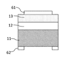
- FIG. 1 is a cross-sectional view of a semiconductor device that can be used in the first embodiment of the present invention.
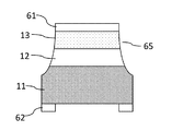
- FIG. 2 is a cross-sectional view showing a process of manufacturing a semiconductor device that can be used in the first embodiment of the present invention.
- FIG. 3 is a cross-sectional view showing the process of manufacturing the semiconductor device, the process of which has advanced from FIG.
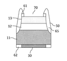
- FIG. 4 is a cross-sectional view showing the process of manufacturing the semiconductor device, the process of which has advanced from FIG.
- FIG. 5 is a cross-sectional view showing the process of manufacturing the semiconductor device, the process of which has advanced from FIG.
- FIG. 6 is a cross-sectional view showing a metal container and a metal-containing glass composition that can be used in each embodiment of the present invention.
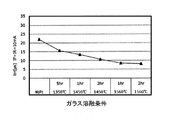
- FIG. 7 is a graph showing the relationship between the heating time and the heating temperature and trr.
- a semiconductor device is a device having a PN junction such as a diode or a thyristor.
- the semiconductor device is provided on a first conductivity type semiconductor substrate 11 having a first conductivity type, and the first conductivity type semiconductor substrate 11, and the first conductivity type semiconductor substrate 11 is more conductive than the first conductivity type semiconductor substrate 11.
- the first conductivity type is, for example, n-type
- the second conductivity type is, for example, p-type.
- the present invention is not limited to this, and the first conductivity type may be p-type and the second conductivity type may be n-type.
- the first conductivity type semiconductor substrate 11 a silicon substrate, a silicon carbide substrate, a gallium nitride substrate or the like can be used, and the impurity concentration thereof is, for example, 1 ⁇ 10 19 cm ⁇ 3 to 1 ⁇ 10 20 cm ⁇ 3 .
- the first conductivity type semiconductor layer 12 is formed by, for example, epitaxial growth on the first conductivity type semiconductor substrate 11, and the impurity concentration in the first conductivity type semiconductor layer 12 is, for example, 5 ⁇ 10 15 cm ⁇ 3 to 1 ⁇ 10 17 cm ⁇ . 3 .
- the thickness of the first conductivity type semiconductor substrate 11 is, for example, 180 ⁇ m, and the thickness of the first conductivity type semiconductor layer 12 is, for example, 50 ⁇ m.
- the second conductivity type semiconductor layer 13 can be formed by implanting, for example, a p-type impurity (for example, boron) into the first conductivity type semiconductor layer 12, and the impurity concentration in the second conductivity type semiconductor layer 13 is, for example, 1 ⁇ 10. 16 cm ⁇ 3 to 1 ⁇ 10 19 cm ⁇ 3 and the thickness is, for example, 8 ⁇ m.
- a p-type impurity for example, boron
- the first electrode 20 may be provided on the front surface of the second conductivity type semiconductor layer 13, and the second electrode 30 may be provided on the back surface of the first conductivity type semiconductor substrate 11.
- the first electrode 20 may be, for example, an anode electrode
- the second electrode 30 may be, for example, a cathode electrode.
- the first electrode 20 may include, for example, an aluminum / silicide film 21, a nickel / silicide film 22, and a Ni (nickel) -P film 23.
- the second electrode 30 may have a nickel film having a silicided film.
- a glass film 50 as a passivation film may be provided around the first electrode 20.
- Such a semiconductor device may be manufactured as follows.
- a first conductivity type semiconductor substrate 11 composed of a first conductivity type, and a first conductivity type provided on the first conductivity type semiconductor substrate 11 and having a first conductivity type impurity concentration lower than that of the first conductivity type semiconductor substrate 11.
- a substrate having a first conductivity type semiconductor layer 12 and a second conductivity type semiconductor layer 13 provided on the first conductivity type semiconductor layer 12 is prepared (see FIG. 2).
- an insulating film 61 made of SiO 2 or the like is formed on the second conductivity type semiconductor layer 13 (see FIG. 2). Further, an insulating film 62 made of SiO 2 or the like is formed on the back surface of the first conductivity type semiconductor substrate 11 (see FIG. 2).
- etching is performed using the formed insulating film 61 as a mask to form a mesa groove 65.
- etching in this embodiment mode, dry etching, wet etching, or the like can be used.
- a protective film (passivation film) made of the glass film 50 is formed so as to cover the formed mesa groove 65 and the insulating film 61.
- openings 70 are formed in the formed insulating film 61 and glass film 50 by etching.
- the first electrode 20 is formed in the opening on the front surface side, and the second electrode 30 is formed on the back surface side (see FIG. 1).
- the glass material which is a raw material for making glass in the metal container 100 (refer FIG. 6) containing a 1st metal and a 2nd metal is thrown in (glass material). Input process).
- the metal container 100 is, for example, a metal crucible.
- the first metal may be gold (Au) and the second metal may be platinum (Pt).
- the first metal may be included at 3 to 10% by weight, and the second metal may be included at 90 to 97% by weight.
- rhodium (Rh) other than gold may be used.
- the metal container 100 may contain a metal other than the first metal and the second metal, may be composed of a ternary alloy of the first metal, the second metal, and the third metal, or may be an alloy of four or more components. It may consist of.
- the glass material has, for example, a content of SiO 2 in the range of 49.5 mol% to 64.3 mol%, a content of Al 2 O 3 in the range of 3.7 mol% to 14.8 mol%, B 2 O 3 content is in the range of 8.4 mol% to 17.9 mol%, ZnO content is in the range of 3.9 mol% to 14.2 mol%, and an alkaline earth metal oxide Is in the range of 7.4 mol% to 12.9 mol%.
- the glass material is melted in the metal container 100 at the first heating temperature for the first time (melting step).
- the metal-containing glass composition 110 containing the first metal, the second metal, or both the first metal and the second metal in the glass composition is generated.
- the first heating temperature may be higher than the melting point of the first metal and lower than the melting point of the second metal.
- the first time is, for example, 1 to 3 hours, and the first heating temperature may be, for example, 1350 ° C. or more and 1700 ° C. or less.
- the melting point of gold is 1064 ° C.
- the melting point of platinum is 1768 ° C.
- the glass film 50 is formed by providing the metal-containing glass composition 110 prepared as described above in a semiconductor layer such as the second conductive semiconductor layer 13 described above (glass film forming step). More specifically, the molten metal-containing glass composition 110 is cooled and then pulverized to a particle size of several ⁇ m, and the pulverized metal-containing glass composition 110 is converted into the first conductive semiconductor substrate 11, the first conductive semiconductor layer 12, After providing in semiconductor layers, such as the 2nd conductivity type semiconductor layer 13, the said metal containing glass composition 110 is fuse
- FIG. 4 FIG.
- the mesa groove 65 is provided up to the first conductivity type semiconductor substrate 11, but is merely an example, and the mesa groove is formed in the first conductivity type semiconductor substrate 11 and the first conductivity type semiconductor layer 12.
- the first conductive semiconductor substrate 11 may be provided with no mesa groove 65.
- the glass film 50 of the present embodiment contains a metal such as a first metal. For this reason, by providing such a glass film 50, a very small amount of metal such as the first metal can be dispersed in the semiconductor layer such as the first conductivity type semiconductor layer 12 that affects the trr control. As a result, the inventors of the present application have confirmed that trr (reverse recovery time) in the semiconductor layer can be set to 5 ⁇ s or more and 15 ⁇ s or less, and the lifetime can be controlled. Note that trr is preferably 5 ⁇ s or more and 11 ⁇ s or less, and more preferably trr is 5 ⁇ s or more and 8 ⁇ s or less. Incidentally, in the conventional embodiment in which heavy metal is added, since a large amount of heavy metal is added as compared with the present embodiment, trr cannot be controlled in units of ⁇ s.
- the glass composition (metal-containing glass composition 110) was provided on the semiconductor layer described above.
- the trr in the semiconductor layer was about 14 ⁇ s. Became.
- the glass composition (metal-containing glass composition 110) was provided on the semiconductor layer described above.
- the trr in the semiconductor layer was about 11 ⁇ s. became.
- the glass composition (metal-containing glass composition 110) was provided on the semiconductor layer, and the trr in the semiconductor layer was about 8 ⁇ s. Became.
- the glass composition (metal-containing glass composition 110) was provided on the semiconductor layer, and the trr in the semiconductor layer was about 8 ⁇ s. Became.
- trr is more preferable to use gold (Au) than rhodium (Rh) as the first metal. This is beneficial because it can be easily controlled.
- trr can be controlled. Further, according to the present embodiment, trr can be controlled in units of ⁇ s. Thus, trr can be controlled in units of ⁇ s while preventing an increase in the manufacturing cost of a semiconductor device such as a chip.
- trr in the semiconductor layer can be adjusted as shown in FIG. 7 by adjusting temperature and time. For this reason, it is only necessary to adjust the temperature and time according to trr required for each semiconductor device, and trr can be adjusted by an extremely simple method. As shown in FIG. 7, trr can be controlled more effectively by adjusting the temperature rather than the time. In particular, heating at 1400 ° C. or higher is preferable, heating at 1500 ° C. or higher is more preferable, and heating at 1550 ° C. or higher is even more preferable.
- the partial switch system (simple PAM) has been a major part of the PFC (Power Factor Correction) section of air conditioners.
- the use of the bridge diode as a partial switch in the simple PAM operation mode is increasing, and improvement of the trr characteristic of the bridge diode is demanded.
- trr may need to be controlled in units of ⁇ s.
- trr When conventional heavy metal diffusion is used, trr can be controlled in units of ns, but it is difficult to control in units of ⁇ s. Although it is possible to control trr in units of ⁇ s by using electron beam irradiation, it is necessary to introduce an expensive machine. In this respect, according to the present embodiment, it is also advantageous in that it can be controlled in units of ⁇ s without introducing an expensive machine.
- the first metal, the second metal, or both the first metal and the second metal can be contained in the glass composition by setting the first heating temperature higher than the melting point of the first metal.
- the first metal and the second metal are alloyed in the metal container 100, the first metal does not melt immediately even when heated to a temperature higher than the melting point of the first metal.
- trr is lowered by raising the temperature in FIG. That is, as described above, the melting point of gold is 1064 ° C., but by increasing the temperature from 1350 ° C. ⁇ 1450 ° C. ⁇ 1560 ° C., trr changes and the amount of metal contained in the glass material is reduced. It is confirmed that the gold melts immediately upon heating to a temperature higher than 1064 ° C. and is not contained within the glass composition.
- the alloy ratio is also important. For example, if the first metal that is gold is contained in an amount of 3 to 10% by weight, and the second metal that is platinum is contained in an amount of 90 to 97% by weight, for example, the trr can be adjusted effectively. Can do. If the amount of the first metal is less than 3% by weight, it may be difficult to contain the metal in the glass composition, and it may be difficult to adjust trr. On the other hand, when the amount of the first metal is more than 10% by weight, the strength as the metal container 100 may be weakened when the heating temperature is increased.
- the metal container 100 including the first metal and the second metal is used.
- a description will be given using a mode in which the first metal and the glass material are put into the metal container 100 containing the second metal.
- adopted in 1st Embodiment are employable also in 2nd Embodiment.
- First metal (typically gold) and glass material are put into a metal container 100 made of the second metal (typically platinum).
- the glass material is melted in the metal container 100 at the first heating temperature for the first time (melting step).
- the metal-containing glass composition 110 containing the first metal is generated by melting the glass material in the metal container 100.
- the first heating temperature may be higher than the melting point of the first metal and lower than the melting point of the second metal.
- the first time is, for example, 1 to 3 hours, and the first heating temperature may be, for example, 1350 ° C. or more and 1700 ° C. or less.
- the glass film 50 is formed by providing the metal-containing glass composition 110 prepared as described above in a semiconductor layer such as the second conductive semiconductor layer 13 described above (glass film forming step).
- the glass film 50 of the present embodiment is mixed with a metal such as the first metal.
- the first metal can be dispersed in the semiconductor layer such as the first conductivity type semiconductor layer 12 that affects trr control.
- the inventors of the present application have confirmed that when the first metal is put into the metal container 100 made of the second metal, the metal container 100 does not melt or has a hole. There were times when I was unhappy. Thus, if there is a hole in the metal container 100, the glass material flows out, which is not suitable for mass production. In particular, since Pt is highly reactive, it is easy to melt or have holes in this way. In addition, when the second metal is Pt, the metal container 100 is very expensive. However, it is difficult to allow a hole in the metal container 100 in terms of cost. Therefore, from this point of view, the first embodiment is more beneficial than the second embodiment.
- First metal (typically gold) and glass material are put into a metal container 100 made of a first metal (typically gold) and a second metal (typically platinum).
- the glass material is melted in the metal container 100 at the first heating temperature for the first time (melting step).
- the metal-containing glass composition 110 containing the first metal, the second metal, or both the first metal and the second metal is generated.
- the first heating temperature may be higher than the melting point of the first metal and lower than the melting point of the second metal.
- the first time is, for example, 1 to 3 hours, and the first heating temperature may be, for example, 1350 ° C. or more and 1700 ° C. or less.
- the glass film 50 is formed by providing the metal-containing glass composition 110 prepared as described above in a semiconductor layer such as the second conductive semiconductor layer 13 described above (glass film forming step).
- the glass film 50 of the present embodiment is mixed with a metal such as the first metal.
- a metal such as a first metal can be dispersed in a semiconductor layer such as the first conductivity type semiconductor layer 12 that affects trr control.
- the fact that the first metal is contained in the glass material means that the first metal is gradually disappearing from the metal container 100. In the present embodiment, it is meaningful to replenish the first metal that has been reduced in this way.
- the first metal may be used when the glass material is melted using the metal container 100 that has been used a predetermined number of times.
- the metal container 100 may have a hole. The amount is very small.
Landscapes
- Formation Of Insulating Films (AREA)
- Bipolar Transistors (AREA)
- Photovoltaic Devices (AREA)
- Glass Compositions (AREA)
Abstract
Description
本発明による半導体装置の製造方法は、
第一金属及び第二金属を含む金属容器内にガラス材料を投入する、又は第二金属を含む金属容器内に第一金属及びガラス材料を投入する工程と、
第一時間の間、第一加熱温度で前記ガラス材料を前記金属容器内で溶融することで、前記第一金属又は前記第二金属を含有する金属含有ガラス組成を生成する工程と、
前記金属含有ガラス組成を半導体層に設ける工程と、
を備えてもよい。
本発明の概念1による半導体装置の製造方法において、
第一時間の間、第一加熱温度で前記ガラス材料を前記金属容器内で溶融することで、前記金属含有ガラス組成内に前記第一金属及び前記第二金属を含有させてもよい。
本発明の概念1又は2による半導体装置の製造方法において、
前記第一加熱温度は、前記第一金属の融点よりも高く、かつ前記第二金属の融点よりも低くてもよい。
本発明の概念1乃至3のいずれか一つによる半導体装置の製造方法において、
前記金属容器は前記第一金属及び前記第二金属を含み、
前記金属容器のうち、前記第一金属は3重量%~10重量%で含まれ、前記第二金属は90重量%~97重量%で含まれてもよい。
本発明の概念1乃至4のいずれか一つによる半導体装置の製造方法において、
前記第一金属は金であり、前記第二金属はプラチナであってもよい。
本発明の概念1乃至5のいずれか一つによる半導体装置の製造方法において、
前記ガラス材料は、SiO2の含有量が49.5mol%~64.3mol%の範囲内にあり、Al2O3の含有量が3.7mol%~14.8mol%の範囲内にあり、B2O3の含有量が8.4mol%~17.9mol%の範囲内にあり、ZnOの含有量が3.9mol%~14.2mol%の範囲内にあり、アルカリ土類金属の酸化物の含有量が7.4mol%~12.9mol%の範囲内にあり、
前記第一時間は1時間~3時間であり、
前記第一加熱温度は1350℃以上1700℃以下であってもよい。
本発明による半導体装置は、
半導体層と、
前記半導体層に設けられたガラス膜と、
を備え、
前記半導体層が分散した金を含み、
前記半導体層は、前記ガラス膜から拡散された金によってライフタイムコントロールされてもよい。
本実施の形態の半導体装置は、ダイオード、サイリスタ等のPN接合を有する装置である。半導体装置は、例えば図1に示すように、第一導電型からなる第一導電型半導体基板11と、第一導電型半導体基板11に設けられ、第一導電型半導体基板11よりも第一導電型の不純物濃度が薄い第一導電型からなる第一導電型半導体層12と、第一導電型半導体層12に設けられる第二導電型半導体層13と、を有してもよい。第一導電型は例えばn型であり、第二導電型は例えばp型である。但し、これに限られることはなく、第一導電型がp型であり、第二導電型がn型であってもよい。
次に、本実施の形態による効果の一例について説明する。なお、「効果」で説明するあらゆる態様を採用することができる。
次に、本発明の第2の実施の形態について説明する。
次に、本発明の第3の実施の形態について説明する。
110 金属含有ガラス組成
Claims (7)
- 第一金属及び第二金属を含む金属容器内にガラス材料を投入する、又は第二金属を含む金属容器内に第一金属及びガラス材料を投入する工程と、
第一時間の間、第一加熱温度で前記ガラス材料を前記金属容器内で溶融することで、前記第一金属又は前記第二金属を含有する金属含有ガラス組成を生成する工程と、
前記金属含有ガラス組成を半導体層に設ける工程と、
を備えたことを特徴とする半導体装置の製造方法。 - 第一時間の間、第一加熱温度で前記ガラス材料を前記金属容器内で溶融することで、前記金属含有ガラス組成内に前記第一金属及び前記第二金属を含有させることを特徴とする請求項1に記載の半導体装置の製造方法。
- 前記第一加熱温度は、前記第一金属の融点よりも高く、かつ前記第二金属の融点よりも低いことを特徴とする請求項1に記載の半導体装置の製造方法。
- 前記金属容器は前記第一金属及び前記第二金属を含み、
前記金属容器のうち、前記第一金属は3重量%~10重量%で含まれ、前記第二金属は90重量%~97重量%で含まれることを特徴とする請求項1に記載の半導体装置の製造方法。 - 前記第一金属は金であり、前記第二金属はプラチナであることを特徴とする請求項1に記載の半導体装置の製造方法。
- 前記ガラス材料は、SiO2の含有量が49.5mol%~64.3mol%の範囲内にあり、Al2O3の含有量が3.7mol%~14.8mol%の範囲内にあり、B2O3の含有量が8.4mol%~17.9mol%の範囲内にあり、ZnOの含有量が3.9mol%~14.2mol%の範囲内にあり、アルカリ土類金属の酸化物の含有量が7.4mol%~12.9mol%の範囲内にあり、
前記第一時間は1時間~3時間であり、
前記第一加熱温度は1350℃以上1700℃以下であることを特徴とする請求項1に記載の半導体装置の製造方法。 - 半導体層と、
前記半導体層に設けられたガラス膜と、
を備え、
前記半導体層は分散した金を含み、
前記半導体層は、前記ガラス膜から拡散された金によってライフタイムコントロールされることを特徴とする半導体装置。
Priority Applications (3)
| Application Number | Priority Date | Filing Date | Title |
|---|---|---|---|
| CN201880010959.XA CN112204716B (zh) | 2018-06-11 | 2018-06-11 | 半导体装置的制造方法以及半导体装置 |
| PCT/JP2018/022158 WO2019239448A1 (ja) | 2018-06-11 | 2018-06-11 | 半導体装置の製造方法及び半導体装置 |
| JP2019537417A JP6764034B2 (ja) | 2018-06-11 | 2018-06-11 | 半導体装置の製造方法及び半導体装置 |
Applications Claiming Priority (1)
| Application Number | Priority Date | Filing Date | Title |
|---|---|---|---|
| PCT/JP2018/022158 WO2019239448A1 (ja) | 2018-06-11 | 2018-06-11 | 半導体装置の製造方法及び半導体装置 |
Publications (1)
| Publication Number | Publication Date |
|---|---|
| WO2019239448A1 true WO2019239448A1 (ja) | 2019-12-19 |
Family
ID=68842526
Family Applications (1)
| Application Number | Title | Priority Date | Filing Date |
|---|---|---|---|
| PCT/JP2018/022158 Ceased WO2019239448A1 (ja) | 2018-06-11 | 2018-06-11 | 半導体装置の製造方法及び半導体装置 |
Country Status (3)
| Country | Link |
|---|---|
| JP (1) | JP6764034B2 (ja) |
| CN (1) | CN112204716B (ja) |
| WO (1) | WO2019239448A1 (ja) |
Citations (6)
| Publication number | Priority date | Publication date | Assignee | Title |
|---|---|---|---|---|
| JPS4965181A (ja) * | 1972-10-25 | 1974-06-24 | ||
| JPS53148986A (en) * | 1977-05-31 | 1978-12-26 | Mitsubishi Electric Corp | Manufacture of semiconductor device |
| JPS5526669A (en) * | 1978-08-15 | 1980-02-26 | Nec Corp | Manufacturing semiconductor device |
| JP2002047095A (ja) * | 2000-07-31 | 2002-02-12 | Shin Etsu Handotai Co Ltd | Gaドープシリコン単結晶の製造方法およびGaドープシリコン単結晶、並びにこれから作製されたシリコン単結晶太陽電池 |
| JP2014187143A (ja) * | 2013-03-22 | 2014-10-02 | Shindengen Electric Mfg Co Ltd | 半導体素子形成用基板、その製造方法、メサ型半導体素子及びその製造方法 |
| WO2018096642A1 (ja) * | 2016-11-25 | 2018-05-31 | 新電元工業株式会社 | 半導体装置の製造方法及び半導体装置 |
Family Cites Families (7)
| Publication number | Priority date | Publication date | Assignee | Title |
|---|---|---|---|---|
| JPS53121464A (en) * | 1977-03-31 | 1978-10-23 | Hitachi Ltd | Glass constituent for semiconductor element surface stabilization |
| JPS5473815A (en) * | 1977-11-24 | 1979-06-13 | Hitachi Ltd | Glass composition for stabilizing semiconductor element surface |
| JPS56114364A (en) * | 1980-02-13 | 1981-09-08 | Nippon Electric Glass Co Ltd | Composite for covering semiconductor device |
| JPS59123238A (ja) * | 1982-12-28 | 1984-07-17 | Fuji Electric Co Ltd | ガラスパシベ−シヨン膜形成法 |
| JPS61150222A (ja) * | 1984-12-24 | 1986-07-08 | Shindengen Electric Mfg Co Ltd | 半導体被覆用ガラス |
| CN102789970A (zh) * | 2012-08-28 | 2012-11-21 | 南通明芯微电子有限公司 | 一种快恢复二极管芯片的制备方法 |
| EP2983197B1 (en) * | 2013-03-29 | 2018-01-31 | Shindengen Electric Manufacturing Co., Ltd. | Glass composition for protecting semiconductor junction, method of manufacturing semiconductor device and semiconductor device |
-
2018
- 2018-06-11 WO PCT/JP2018/022158 patent/WO2019239448A1/ja not_active Ceased
- 2018-06-11 CN CN201880010959.XA patent/CN112204716B/zh active Active
- 2018-06-11 JP JP2019537417A patent/JP6764034B2/ja active Active
Patent Citations (6)
| Publication number | Priority date | Publication date | Assignee | Title |
|---|---|---|---|---|
| JPS4965181A (ja) * | 1972-10-25 | 1974-06-24 | ||
| JPS53148986A (en) * | 1977-05-31 | 1978-12-26 | Mitsubishi Electric Corp | Manufacture of semiconductor device |
| JPS5526669A (en) * | 1978-08-15 | 1980-02-26 | Nec Corp | Manufacturing semiconductor device |
| JP2002047095A (ja) * | 2000-07-31 | 2002-02-12 | Shin Etsu Handotai Co Ltd | Gaドープシリコン単結晶の製造方法およびGaドープシリコン単結晶、並びにこれから作製されたシリコン単結晶太陽電池 |
| JP2014187143A (ja) * | 2013-03-22 | 2014-10-02 | Shindengen Electric Mfg Co Ltd | 半導体素子形成用基板、その製造方法、メサ型半導体素子及びその製造方法 |
| WO2018096642A1 (ja) * | 2016-11-25 | 2018-05-31 | 新電元工業株式会社 | 半導体装置の製造方法及び半導体装置 |
Also Published As
| Publication number | Publication date |
|---|---|
| CN112204716B (zh) | 2025-03-11 |
| JP6764034B2 (ja) | 2020-09-30 |
| CN112204716A (zh) | 2021-01-08 |
| JPWO2019239448A1 (ja) | 2020-06-25 |
Similar Documents
| Publication | Publication Date | Title |
|---|---|---|
| JP5631497B1 (ja) | 半導体接合保護用ガラス組成物、半導体装置の製造方法及び半導体装置 | |
| CN104025303B (zh) | 使用硅纳米颗粒制造太阳能电池的激光接触工艺、激光系统和太阳能电池结构 | |
| CN115602355B (zh) | 导电浆料及其制备的太阳能电池 | |
| US9941112B2 (en) | Method of manufacturing semiconductor device and semiconductor device | |
| JP3820424B2 (ja) | 不純物イオン注入層の活性化法 | |
| JP5340511B1 (ja) | 半導体装置の製造方法及び半導体装置 | |
| TW201210052A (en) | Back junction solar cell with selective front surface field | |
| WO2013168521A1 (ja) | 樹脂封止型半導体装置及びその製造方法 | |
| KR101851884B1 (ko) | 반도체 장치의 제조 방법 및 유리 피막 형성 장치 | |
| TW201643943A (zh) | 鑽石型半導體系統及方法 | |
| WO2013168623A1 (ja) | 半導体接合保護用ガラス組成物、半導体装置の製造方法及び半導体装置 | |
| CN106611797A (zh) | 一种具有局域金属寿命控制的功率器件及其制作方法 | |
| JP6764034B2 (ja) | 半導体装置の製造方法及び半導体装置 | |
| CN103943495A (zh) | 金属与n型硅肖特基接触势垒高度的调节方法 | |
| TWI720544B (zh) | 半導體裝置的製造方法 | |
| CN104637803B (zh) | 改善igbt背面金属化的工艺方法 | |
| CN110061052A (zh) | 高正向阻断电压门极灵敏触发单向可控硅芯片和制造方法 | |
| JP5848821B2 (ja) | 半導体接合保護用ガラス組成物、半導体装置の製造方法、半導体装置及び半導体接合保護用ガラス組成物の製造方法 | |
| JP2020102547A (ja) | 半導体装置およびその製造方法 | |
| JP2725790B2 (ja) | 半導体装置の製造方法 | |
| WO2025115789A1 (ja) | 半導体装置の製造方法及び半導体装置 | |
| JP5655139B2 (ja) | 半導体装置の製造方法及び半導体装置 | |
| JP5303008B2 (ja) | 半導体素子及び半導体素子の製造方法 | |
| JPWO2013168521A1 (ja) | 樹脂封止型半導体装置及びその製造方法 | |
| JPS5994415A (ja) | 半導体装置の製法 |
Legal Events
| Date | Code | Title | Description |
|---|---|---|---|
| ENP | Entry into the national phase |
Ref document number: 2019537417 Country of ref document: JP Kind code of ref document: A |
|
| 121 | Ep: the epo has been informed by wipo that ep was designated in this application |
Ref document number: 18922205 Country of ref document: EP Kind code of ref document: A1 |
|
| NENP | Non-entry into the national phase |
Ref country code: DE |
|
| 122 | Ep: pct application non-entry in european phase |
Ref document number: 18922205 Country of ref document: EP Kind code of ref document: A1 |
|
| WWG | Wipo information: grant in national office |
Ref document number: 201880010959.X Country of ref document: CN |