WO2019216196A1 - 表示装置及び表示装置の製造方法、並びに、電子機器 - Google Patents
表示装置及び表示装置の製造方法、並びに、電子機器 Download PDFInfo
- Publication number
- WO2019216196A1 WO2019216196A1 PCT/JP2019/017175 JP2019017175W WO2019216196A1 WO 2019216196 A1 WO2019216196 A1 WO 2019216196A1 JP 2019017175 W JP2019017175 W JP 2019017175W WO 2019216196 A1 WO2019216196 A1 WO 2019216196A1
- Authority
- WO
- WIPO (PCT)
- Prior art keywords
- light emitting
- pixel
- recess
- display device
- recesses
- Prior art date
- Legal status (The legal status is an assumption and is not a legal conclusion. Google has not performed a legal analysis and makes no representation as to the accuracy of the status listed.)
- Ceased
Links
Images








Classifications
-
- H—ELECTRICITY
- H10—SEMICONDUCTOR DEVICES; ELECTRIC SOLID-STATE DEVICES NOT OTHERWISE PROVIDED FOR
- H10K—ORGANIC ELECTRIC SOLID-STATE DEVICES
- H10K59/00—Integrated devices, or assemblies of multiple devices, comprising at least one organic light-emitting element covered by group H10K50/00
- H10K59/30—Devices specially adapted for multicolour light emission
- H10K59/35—Devices specially adapted for multicolour light emission comprising red-green-blue [RGB] subpixels
- H10K59/351—Devices specially adapted for multicolour light emission comprising red-green-blue [RGB] subpixels comprising more than three subpixels, e.g. red-green-blue-white [RGBW]
-
- G—PHYSICS
- G09—EDUCATION; CRYPTOGRAPHY; DISPLAY; ADVERTISING; SEALS
- G09F—DISPLAYING; ADVERTISING; SIGNS; LABELS OR NAME-PLATES; SEALS
- G09F9/00—Indicating arrangements for variable information in which the information is built-up on a support by selection or combination of individual elements
-
- G—PHYSICS
- G09—EDUCATION; CRYPTOGRAPHY; DISPLAY; ADVERTISING; SEALS
- G09F—DISPLAYING; ADVERTISING; SIGNS; LABELS OR NAME-PLATES; SEALS
- G09F9/00—Indicating arrangements for variable information in which the information is built-up on a support by selection or combination of individual elements
- G09F9/30—Indicating arrangements for variable information in which the information is built-up on a support by selection or combination of individual elements in which the desired character or characters are formed by combining individual elements
-
- H—ELECTRICITY
- H05—ELECTRIC TECHNIQUES NOT OTHERWISE PROVIDED FOR
- H05B—ELECTRIC HEATING; ELECTRIC LIGHT SOURCES NOT OTHERWISE PROVIDED FOR; CIRCUIT ARRANGEMENTS FOR ELECTRIC LIGHT SOURCES, IN GENERAL
- H05B33/00—Electroluminescent light sources
- H05B33/10—Apparatus or processes specially adapted to the manufacture of electroluminescent light sources
-
- H—ELECTRICITY
- H05—ELECTRIC TECHNIQUES NOT OTHERWISE PROVIDED FOR
- H05B—ELECTRIC HEATING; ELECTRIC LIGHT SOURCES NOT OTHERWISE PROVIDED FOR; CIRCUIT ARRANGEMENTS FOR ELECTRIC LIGHT SOURCES, IN GENERAL
- H05B33/00—Electroluminescent light sources
- H05B33/12—Light sources with substantially two-dimensional [2D] radiating surfaces
-
- H—ELECTRICITY
- H05—ELECTRIC TECHNIQUES NOT OTHERWISE PROVIDED FOR
- H05B—ELECTRIC HEATING; ELECTRIC LIGHT SOURCES NOT OTHERWISE PROVIDED FOR; CIRCUIT ARRANGEMENTS FOR ELECTRIC LIGHT SOURCES, IN GENERAL
- H05B33/00—Electroluminescent light sources
- H05B33/12—Light sources with substantially two-dimensional [2D] radiating surfaces
- H05B33/22—Light sources with substantially two-dimensional [2D] radiating surfaces characterised by the chemical or physical composition or the arrangement of auxiliary dielectric or reflective layers
-
- H—ELECTRICITY
- H10—SEMICONDUCTOR DEVICES; ELECTRIC SOLID-STATE DEVICES NOT OTHERWISE PROVIDED FOR
- H10K—ORGANIC ELECTRIC SOLID-STATE DEVICES
- H10K50/00—Organic light-emitting devices
- H10K50/80—Constructional details
- H10K50/805—Electrodes
- H10K50/81—Anodes
- H10K50/818—Reflective anodes, e.g. ITO combined with thick metallic layers
-
- H—ELECTRICITY
- H10—SEMICONDUCTOR DEVICES; ELECTRIC SOLID-STATE DEVICES NOT OTHERWISE PROVIDED FOR
- H10K—ORGANIC ELECTRIC SOLID-STATE DEVICES
- H10K50/00—Organic light-emitting devices
- H10K50/80—Constructional details
- H10K50/805—Electrodes
- H10K50/82—Cathodes
- H10K50/828—Transparent cathodes, e.g. comprising thin metal layers
-
- H—ELECTRICITY
- H10—SEMICONDUCTOR DEVICES; ELECTRIC SOLID-STATE DEVICES NOT OTHERWISE PROVIDED FOR
- H10K—ORGANIC ELECTRIC SOLID-STATE DEVICES
- H10K59/00—Integrated devices, or assemblies of multiple devices, comprising at least one organic light-emitting element covered by group H10K50/00
- H10K59/10—OLED displays
- H10K59/12—Active-matrix OLED [AMOLED] displays
- H10K59/122—Pixel-defining structures or layers, e.g. banks
-
- H—ELECTRICITY
- H10—SEMICONDUCTOR DEVICES; ELECTRIC SOLID-STATE DEVICES NOT OTHERWISE PROVIDED FOR
- H10K—ORGANIC ELECTRIC SOLID-STATE DEVICES
- H10K59/00—Integrated devices, or assemblies of multiple devices, comprising at least one organic light-emitting element covered by group H10K50/00
- H10K59/30—Devices specially adapted for multicolour light emission
- H10K59/35—Devices specially adapted for multicolour light emission comprising red-green-blue [RGB] subpixels
- H10K59/352—Devices specially adapted for multicolour light emission comprising red-green-blue [RGB] subpixels the areas of the RGB subpixels being different
-
- H—ELECTRICITY
- H10—SEMICONDUCTOR DEVICES; ELECTRIC SOLID-STATE DEVICES NOT OTHERWISE PROVIDED FOR
- H10K—ORGANIC ELECTRIC SOLID-STATE DEVICES
- H10K59/00—Integrated devices, or assemblies of multiple devices, comprising at least one organic light-emitting element covered by group H10K50/00
- H10K59/30—Devices specially adapted for multicolour light emission
- H10K59/35—Devices specially adapted for multicolour light emission comprising red-green-blue [RGB] subpixels
- H10K59/353—Devices specially adapted for multicolour light emission comprising red-green-blue [RGB] subpixels characterised by the geometrical arrangement of the RGB subpixels
-
- H—ELECTRICITY
- H10—SEMICONDUCTOR DEVICES; ELECTRIC SOLID-STATE DEVICES NOT OTHERWISE PROVIDED FOR
- H10K—ORGANIC ELECTRIC SOLID-STATE DEVICES
- H10K71/00—Manufacture or treatment specially adapted for the organic devices covered by this subclass
-
- H—ELECTRICITY
- H10—SEMICONDUCTOR DEVICES; ELECTRIC SOLID-STATE DEVICES NOT OTHERWISE PROVIDED FOR
- H10K—ORGANIC ELECTRIC SOLID-STATE DEVICES
- H10K71/00—Manufacture or treatment specially adapted for the organic devices covered by this subclass
- H10K71/10—Deposition of organic active material
- H10K71/16—Deposition of organic active material using physical vapour deposition [PVD], e.g. vacuum deposition or sputtering
- H10K71/164—Deposition of organic active material using physical vapour deposition [PVD], e.g. vacuum deposition or sputtering using vacuum deposition
-
- G—PHYSICS
- G09—EDUCATION; CRYPTOGRAPHY; DISPLAY; ADVERTISING; SEALS
- G09G—ARRANGEMENTS OR CIRCUITS FOR CONTROL OF INDICATING DEVICES USING STATIC MEANS TO PRESENT VARIABLE INFORMATION
- G09G2300/00—Aspects of the constitution of display devices
- G09G2300/04—Structural and physical details of display devices
- G09G2300/0439—Pixel structures
- G09G2300/0452—Details of colour pixel setup, e.g. pixel composed of a red, a blue and two green components
-
- G—PHYSICS
- G09—EDUCATION; CRYPTOGRAPHY; DISPLAY; ADVERTISING; SEALS
- G09G—ARRANGEMENTS OR CIRCUITS FOR CONTROL OF INDICATING DEVICES USING STATIC MEANS TO PRESENT VARIABLE INFORMATION
- G09G2310/00—Command of the display device
- G09G2310/02—Addressing, scanning or driving the display screen or processing steps related thereto
- G09G2310/0202—Addressing of scan or signal lines
-
- G—PHYSICS
- G09—EDUCATION; CRYPTOGRAPHY; DISPLAY; ADVERTISING; SEALS
- G09G—ARRANGEMENTS OR CIRCUITS FOR CONTROL OF INDICATING DEVICES USING STATIC MEANS TO PRESENT VARIABLE INFORMATION
- G09G2310/00—Command of the display device
- G09G2310/02—Addressing, scanning or driving the display screen or processing steps related thereto
- G09G2310/0264—Details of driving circuits
- G09G2310/0286—Details of a shift registers arranged for use in a driving circuit
-
- G—PHYSICS
- G09—EDUCATION; CRYPTOGRAPHY; DISPLAY; ADVERTISING; SEALS
- G09G—ARRANGEMENTS OR CIRCUITS FOR CONTROL OF INDICATING DEVICES USING STATIC MEANS TO PRESENT VARIABLE INFORMATION
- G09G3/00—Control arrangements or circuits, of interest only in connection with visual indicators other than cathode-ray tubes
- G09G3/20—Control arrangements or circuits, of interest only in connection with visual indicators other than cathode-ray tubes for presentation of an assembly of a number of characters, e.g. a page, by composing the assembly by combination of individual elements arranged in a matrix no fixed position being assigned to or needed to be assigned to the individual characters or partial characters
- G09G3/2003—Display of colours
-
- G—PHYSICS
- G09—EDUCATION; CRYPTOGRAPHY; DISPLAY; ADVERTISING; SEALS
- G09G—ARRANGEMENTS OR CIRCUITS FOR CONTROL OF INDICATING DEVICES USING STATIC MEANS TO PRESENT VARIABLE INFORMATION
- G09G3/00—Control arrangements or circuits, of interest only in connection with visual indicators other than cathode-ray tubes
- G09G3/20—Control arrangements or circuits, of interest only in connection with visual indicators other than cathode-ray tubes for presentation of an assembly of a number of characters, e.g. a page, by composing the assembly by combination of individual elements arranged in a matrix no fixed position being assigned to or needed to be assigned to the individual characters or partial characters
- G09G3/22—Control arrangements or circuits, of interest only in connection with visual indicators other than cathode-ray tubes for presentation of an assembly of a number of characters, e.g. a page, by composing the assembly by combination of individual elements arranged in a matrix no fixed position being assigned to or needed to be assigned to the individual characters or partial characters using controlled light sources
- G09G3/30—Control arrangements or circuits, of interest only in connection with visual indicators other than cathode-ray tubes for presentation of an assembly of a number of characters, e.g. a page, by composing the assembly by combination of individual elements arranged in a matrix no fixed position being assigned to or needed to be assigned to the individual characters or partial characters using controlled light sources using electroluminescent panels
- G09G3/32—Control arrangements or circuits, of interest only in connection with visual indicators other than cathode-ray tubes for presentation of an assembly of a number of characters, e.g. a page, by composing the assembly by combination of individual elements arranged in a matrix no fixed position being assigned to or needed to be assigned to the individual characters or partial characters using controlled light sources using electroluminescent panels semiconductive, e.g. using light-emitting diodes [LED]
- G09G3/3208—Control arrangements or circuits, of interest only in connection with visual indicators other than cathode-ray tubes for presentation of an assembly of a number of characters, e.g. a page, by composing the assembly by combination of individual elements arranged in a matrix no fixed position being assigned to or needed to be assigned to the individual characters or partial characters using controlled light sources using electroluminescent panels semiconductive, e.g. using light-emitting diodes [LED] organic, e.g. using organic light-emitting diodes [OLED]
- G09G3/3225—Control arrangements or circuits, of interest only in connection with visual indicators other than cathode-ray tubes for presentation of an assembly of a number of characters, e.g. a page, by composing the assembly by combination of individual elements arranged in a matrix no fixed position being assigned to or needed to be assigned to the individual characters or partial characters using controlled light sources using electroluminescent panels semiconductive, e.g. using light-emitting diodes [LED] organic, e.g. using organic light-emitting diodes [OLED] using an active matrix
- G09G3/3233—Control arrangements or circuits, of interest only in connection with visual indicators other than cathode-ray tubes for presentation of an assembly of a number of characters, e.g. a page, by composing the assembly by combination of individual elements arranged in a matrix no fixed position being assigned to or needed to be assigned to the individual characters or partial characters using controlled light sources using electroluminescent panels semiconductive, e.g. using light-emitting diodes [LED] organic, e.g. using organic light-emitting diodes [OLED] using an active matrix with pixel circuitry controlling the current through the light-emitting element
-
- H—ELECTRICITY
- H10—SEMICONDUCTOR DEVICES; ELECTRIC SOLID-STATE DEVICES NOT OTHERWISE PROVIDED FOR
- H10K—ORGANIC ELECTRIC SOLID-STATE DEVICES
- H10K2102/00—Constructional details relating to the organic devices covered by this subclass
- H10K2102/301—Details of OLEDs
- H10K2102/302—Details of OLEDs of OLED structures
- H10K2102/3023—Direction of light emission
- H10K2102/3026—Top emission
-
- H—ELECTRICITY
- H10—SEMICONDUCTOR DEVICES; ELECTRIC SOLID-STATE DEVICES NOT OTHERWISE PROVIDED FOR
- H10K—ORGANIC ELECTRIC SOLID-STATE DEVICES
- H10K59/00—Integrated devices, or assemblies of multiple devices, comprising at least one organic light-emitting element covered by group H10K50/00
- H10K59/10—OLED displays
- H10K59/12—Active-matrix OLED [AMOLED] displays
- H10K59/1201—Manufacture or treatment
-
- H—ELECTRICITY
- H10—SEMICONDUCTOR DEVICES; ELECTRIC SOLID-STATE DEVICES NOT OTHERWISE PROVIDED FOR
- H10K—ORGANIC ELECTRIC SOLID-STATE DEVICES
- H10K59/00—Integrated devices, or assemblies of multiple devices, comprising at least one organic light-emitting element covered by group H10K50/00
- H10K59/10—OLED displays
- H10K59/12—Active-matrix OLED [AMOLED] displays
- H10K59/123—Connection of the pixel electrodes to the thin film transistors [TFT]
-
- H—ELECTRICITY
- H10—SEMICONDUCTOR DEVICES; ELECTRIC SOLID-STATE DEVICES NOT OTHERWISE PROVIDED FOR
- H10K—ORGANIC ELECTRIC SOLID-STATE DEVICES
- H10K59/00—Integrated devices, or assemblies of multiple devices, comprising at least one organic light-emitting element covered by group H10K50/00
- H10K59/80—Constructional details
- H10K59/805—Electrodes
- H10K59/8051—Anodes
- H10K59/80515—Anodes characterised by their shape
-
- H—ELECTRICITY
- H10—SEMICONDUCTOR DEVICES; ELECTRIC SOLID-STATE DEVICES NOT OTHERWISE PROVIDED FOR
- H10K—ORGANIC ELECTRIC SOLID-STATE DEVICES
- H10K59/00—Integrated devices, or assemblies of multiple devices, comprising at least one organic light-emitting element covered by group H10K50/00
- H10K59/80—Constructional details
- H10K59/875—Arrangements for extracting light from the devices
- H10K59/878—Arrangements for extracting light from the devices comprising reflective means
Definitions
- the present disclosure relates to a display device, a method for manufacturing the display device, and an electronic apparatus.
- flat panel display devices are the mainstream.
- a display device that uses a so-called current-driven electro-optical element whose light emission luminance changes according to a current value flowing through the device as a light-emitting portion (light-emitting element) of a pixel.
- a current-driven electro-optical element an organic EL element using a phenomenon in which light is emitted when an electric field is applied to an organic thin film using electroluminescence (EL) of an organic material is known.
- the organic EL element is formed by vapor-depositing an organic EL material on the anode electrode.
- an organic EL material is formed by vapor-depositing an organic EL material on the anode electrode.
- there is a separate coloring method in which elements of each color of R (red), G (green), and B (blue) are individually patterned.
- this separate coating method it is necessary to deposit an organic EL material by masking the electrode openings of other colors for each of the RGB colors. For this reason, the mask alignment accuracy limits the pixel pitch. From the viewpoint of mask accuracy, it is difficult to achieve high definition, and this tendency becomes more prominent as the pixel pitch becomes smaller.
- the multi-face structure having an inclined surface on which the light emitting element is formed is a protrusion formed in a state of protruding on the substrate.
- the light emitting elements are formed on the inclined surface of the multi-face structure that is the protrusion on the substrate, light is emitted from the light emitting elements of each color in the direction away from the center of the pixel, that is, in the direction of diffusion. Therefore, the light extraction efficiency is lowered and the viewing angle is dependent.
- the present disclosure provides a display device and a display device manufacturing method capable of increasing the definition with a separate coating method and increasing light extraction efficiency, and an electronic apparatus including the display device. Objective.
- a display device of the present disclosure is provided.
- a plurality of recesses provided on the pixel formation surface; and A pixel disposed in each of the plurality of recesses, The light emitting portion of the pixel is formed on the side wall and the bottom surface of each of the plurality of recesses.
- a manufacturing method of the display device of the present disclosure for achieving the above-described object is as follows.
- a plurality of recesses provided on the pixel formation surface; and
- a light emitting portion of the pixel is formed on the side wall and the bottom surface of each of the plurality of recesses.
- an electronic apparatus for achieving the above object includes the display device having the above structure.
- FIG. 1 is a system configuration diagram illustrating an outline of a configuration of an organic EL display device to which the technology of the present disclosure is applied.
- FIG. 2 is a circuit diagram illustrating an example of a circuit configuration of a pixel (pixel circuit) in an organic EL display device to which the technology of the present disclosure is applied.
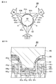
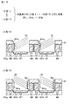
- FIG. 3A is a plan view showing the pixel structure according to the first embodiment, and FIG. 3B is a cross-sectional view showing a cross-sectional structure along the line AA in FIG. 3A.
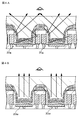
- FIG. 4A is a schematic diagram illustrating how light is emitted from the G sub-pixel, and FIG. 4B is a schematic diagram illustrating how light is emitted from the W sub-pixel.
- FIG. 1 is a system configuration diagram illustrating an outline of a configuration of an organic EL display device to which the technology of the present disclosure is applied.
- FIG. 2 is a circuit diagram illustrating an example of a circuit configuration of a pixel (pixel circuit) in an organic
- FIG. 5 is an explanatory diagram for setting the incident limit angle of oblique deposition.
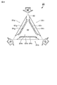
- FIG. 6 is a plan view illustrating the pixel structure according to the second embodiment.
- FIG. 7 is a process diagram (part 1) illustrating the flow of steps of a method for manufacturing a pixel structure according to the third embodiment.
- FIG. 8 is a process diagram (part 2) illustrating the flow of the process of the manufacturing method of the pixel structure according to the third embodiment.
- FIG. 9 is a process diagram (part 3) illustrating the flow of the process of the manufacturing method of the pixel structure according to the third embodiment.
- FIG. 10 is a process diagram (part 4) illustrating the flow of the process of the manufacturing method of the pixel structure according to the third embodiment.
- FIG. 1 is a plan view illustrating the pixel structure according to the second embodiment.
- FIG. 7 is a process diagram (part 1) illustrating the flow of steps of a method for manufacturing a pixel structure according to the third embodiment.
- FIG. 8 is a
- FIG. 11 is a process diagram (part 5) illustrating the flow of the process of the manufacturing method of the pixel structure according to the third embodiment.
- 12A is a plan view showing a pixel structure according to Example 4, and
- FIG. 12B is a sectional end view taken along line BB of FIG. 12A.
- FIG. 13 is a schematic diagram illustrating a state of emission of light from the B sub-pixel.
- FIG. 14 is a plan view showing a pixel structure according to Example 5.
- FIGS. 14A, 14B, and 14C show other examples of the shape of the side anode electrode.
- FIG. 15 is a process diagram (part 1) illustrating the flow of steps of a method for manufacturing a pixel structure according to the sixth embodiment.
- FIG. 15 is a process diagram (part 1) illustrating the flow of steps of a method for manufacturing a pixel structure according to the sixth embodiment.
- FIG. 16 is a process diagram (part 2) illustrating the flow of the process of the manufacturing method of the pixel structure according to the sixth embodiment.
- 17A is a front view of an interchangeable-lens single-lens reflex digital still camera according to the first specific example of the electronic apparatus of the present disclosure
- FIG. 17B is a rear view thereof.
- FIG. 18 is an external view illustrating an example of a head-mounted display according to the specific example 2 of the electronic apparatus of the present disclosure.
- Example 1 (example in which a pixel is composed of four sub-pixels of RGBW) 3-2.
- Example 2 (Modification of Example 1: Another example of the shape of the recess) 3-3.
- Example 3 (Example of manufacturing method of pixel structure according to Example 1) 3-4.
- Example 4 (Example in which a pixel is composed of three sub-pixels of RGB) 3-5.
- Example 5 (Modification of Example 4: Another example of shape of side anode electrode) 3-6.
- Example 6 (Example of manufacturing method of pixel structure according to Example 4) 4). Modification 5 5.
- Example 2 (example of head mounted display) 6). Configurations that can be taken by the present disclosure
- the pixel may include a plurality of light emitting units having different emission colors. And one of a some light emission part can be set as the structure currently formed in each bottom face of a some recessed part.
- the light emission colors of the plurality of light emitting units include four colors of red, green, blue, and white.
- the green and blue light emitting portions may be formed on the sidewalls of the plurality of recesses, and the white light emitting portions may be formed on the bottom surfaces of the plurality of recesses.
- the light emitting layer of the light emitting portion formed on the side wall of the concave portion is oblique to the side wall of the concave portion. It can be set as the structure formed into a film by vapor deposition. In oblique deposition, the incident angle of the light emitting material with respect to the bottom surface of the recess is preferably set to an angle at which the light emitting layer is formed on the side wall and the bottom surface of the recess. The incident angle of the light emitting material can be set based on the size of the side anode electrode formed on the side wall of the recess and the size of the bottom anode electrode formed on the bottom surface of the recess.
- the light emission colors of the plurality of light emitting units include two colors of red, green, and blue
- the light emitting part of two colors of the three colors can be formed on the side wall of each of the plurality of recesses, and the light emitting part of the remaining one color can be formed on the bottom surface of each of the plurality of recesses.
- the light emitting layer of the light emitting portion formed on the side wall of the concave portion is oblique to the side wall of the concave portion. It can be set as the structure formed into a film by vapor deposition. In oblique deposition, the incident angle of the luminescent material with respect to the bottom surface of the recess is preferably set to an angle at which the light emitting layer is not formed on the bottom surface of the recess.
- the light emitting portion of the pixel can be configured by an organic electroluminescence element.
- a display device to which the technology of the present disclosure is applied is an active matrix display device in which a current flowing through an electro-optical element is controlled by an active element provided in the same pixel circuit as the electro-optical element, for example, an insulated gate field effect transistor It is.
- the insulated gate field effect transistor include a MOS (Metal Oxide Semiconductor) transistor and a TFT (Thin Film Transistor).
- an active matrix organic EL that uses, for example, an organic EL element, which is a current-driven electro-optical element whose emission luminance changes according to the current value flowing through the device, as a light emitting portion (light emitting element) of a pixel circuit.
- an organic EL element which is a current-driven electro-optical element whose emission luminance changes according to the current value flowing through the device, as a light emitting portion (light emitting element) of a pixel circuit.
- a display device will be described as an example.
- FIG. 1 is a system configuration diagram illustrating an outline of a configuration of an organic EL display device to which the technology of the present disclosure is applied.
- an organic EL display device 10 according to this application example includes a pixel array unit 30 in which a plurality of pixels 20 including organic EL elements are two-dimensionally arranged in a matrix, and the pixel array unit 30. It has the structure which has the peripheral circuit part which drives each pixel 20 of these.
- the organic EL display device 10 is a display device compatible with color display.
- the pixel 20 is a main pixel that is a unit for forming a color image, and includes a plurality of sub-pixels having different emission colors.
- the pixel 20 includes a sub pixel 20r that emits red (Red) light, a sub pixel 20g that emits green (Green) light, a sub pixel 20b that emits blue (B) light, and
- the sub-pixel 20w emits white (W) light and is composed of four sub-pixels.
- the sub-pixels 20r, 20g, 20b, and 20w are arranged in a grid, for example.
- the arrangement of each of the sub-pixels 20r, 20g, 20b, and 20w is not limited to the color arrangement shown in FIG.
- the sub-pixels 20r, 20g, 20b, and 20w may be collectively referred to as a sub-pixel 20s.
- the peripheral circuit unit includes, for example, a writing scanning unit 40, a driving scanning unit 50, a signal output unit 60, and the like mounted on the same display panel 70 as the pixel array unit 30, and each sub pixel 20s of the pixel array unit 30. Drive. It is also possible to adopt a configuration in which some or all of the writing scanning unit 40, the driving scanning unit 50, and the signal output unit 60 are provided outside the display panel 70.
- an insulating transparent substrate such as a glass substrate can be used, or a semiconductor substrate such as a silicon substrate can be used.
- An organic EL display device using a semiconductor substrate such as a silicon substrate as a substrate of the display panel 70 is called a so-called micro display (small display), and an electronic viewfinder of a digital still camera, a display unit of a head mounted display, or the like. It is suitable for use as.
- the pixel array unit 30 includes a scanning line 31 (31 1 to 31 m ) and a drive along the row direction (pixel arrangement direction / horizontal direction of pixels in the pixel row) with respect to the arrangement of the m pixels and the n columns of sub pixels 20s.
- a line 32 (32 1 to 32 m ) is wired for each pixel row.
- signal lines 33 (33 1 to 33 n ) are wired for each pixel column along the column direction (pixel array direction / vertical direction) of the m rows and n columns of sub-pixels 20s. ing.
- the scanning lines 31 1 to 31 m are connected to the output ends of the corresponding rows of the writing scanning unit 40, respectively.
- the drive lines 32 1 to 32 m are connected to the output ends of the corresponding rows of the drive scanning unit 50, respectively.
- the signal lines 33 1 to 33 n are connected to the output ends of the corresponding columns of the signal output unit 60, respectively.
- the write scanning unit 40 is configured by a shift register circuit, an address decoder, and the like.
- the writing scanning unit 40 writes the write scanning signal WS (WS 1 to WS m ) to the scanning lines 31 (31 1 to 31 m ) when writing the signal voltage of the video signal to each sub-pixel 20s of the pixel array unit 30. ) Is sequentially supplied, the so-called line-sequential scanning is performed in which the sub-pixels 20s of the pixel array unit 30 are sequentially scanned in units of rows.
- the drive scanning unit 50 is configured by a shift register circuit, an address decoder, and the like, similarly to the writing scanning unit 40.
- the drive scanning unit 50 supplies the light emission control signals DS (DS 1 to DS m ) to the drive lines 32 (32 1 to 32 m ) in synchronization with the line sequential scanning by the writing scanning unit 40.
- the light emission / non-light emission (quenching) of the pixel 20s is controlled.
- the signal output unit 60 includes a signal voltage V sig and a reference voltage V ofs of a video signal corresponding to luminance information supplied from a signal supply source (not shown) (hereinafter may be simply referred to as “signal voltage”). And are selectively output.
- the reference voltage V ofs is a voltage corresponding to a reference voltage of the signal voltage V sig of the video signal (for example, a voltage corresponding to the black level of the video signal) or a voltage in the vicinity thereof.
- the reference voltage V ofs is used as an initialization voltage when performing the correction operation.
- the signal voltage V sig / reference voltage V ofs alternatively output from the signal output unit 60 is written to each sub-pixel 20s of the pixel array unit 30 via the signal line 34 (34 1 to 34 n ). Writing is performed in units of pixel rows selected by line sequential scanning by the scanning unit 40. In other words, the signal output unit 60 adopts a line sequential writing driving form in which the signal voltage V sig is written in units of pixel rows.
- FIG. 2 is a circuit diagram illustrating an example of a circuit configuration of a pixel (pixel circuit) in the organic EL display device 10 to which the technology of the present disclosure is applied.
- the light emitting portion of the sub-pixel 20 s is composed of the organic EL element 21.
- the organic EL element 21 is an example of a current-driven electro-optical element whose emission luminance changes according to the value of current flowing through the device.
- the sub-pixel 20 s includes an organic EL element 21 and a drive circuit (pixel drive circuit) that drives the organic EL element 21 by passing a current through the organic EL element 21.
- the organic EL element 21 has a cathode electrode connected to a common power line 34 wired in common to all the sub-pixels 20s.
- C el is an equivalent capacitance of the organic EL element 21.
- the drive circuit for driving the organic EL element 21 has a configuration including a drive transistor 22, a sampling transistor 23, a light emission control transistor 24, a storage capacitor 25, and an auxiliary capacitor 26.
- the organic EL element 21 and its driving circuit are formed on a semiconductor substrate such as a silicon substrate instead of an insulator such as a glass substrate, and a P-channel transistor is used as the driving transistor 22.
- the structure using is adopted.
- the sampling transistor 23 and the light emission control transistor 24 are also configured to use P-channel type transistors, like the drive transistor 22. Therefore, the drive transistor 22, the sampling transistor 23, and the light emission control transistor 24 have four terminals of source / gate / drain / back gate instead of three terminals of source / gate / drain. A power supply voltage V dd is applied to the back gate.
- sampling transistor 23 and the light emission control transistor 24 are switching transistors that function as switching elements, they are not limited to P-channel transistors. Therefore, the sampling transistor 23 and the light emission control transistor 24 may be an N-channel transistor or a configuration in which a P-channel type and an N-channel type are mixed.
- the sampling transistor 23 writes the signal voltage V sig of the video signal supplied from the signal output unit 60 through the signal line 33 to the storage capacitor 25.
- the light emission control transistor 24 is connected between the node of the power supply voltage Vdd and the source electrode of the drive transistor 22 and controls light emission / non-light emission of the organic EL element 21 under the drive by the light emission control signal DS.
- the storage capacitor 25 is connected between the gate electrode and the source electrode of the drive transistor 22.
- the holding capacitor 25 holds the signal voltage V sig of the video signal written by sampling by the sampling transistor 23.
- the driving transistor 22 drives the organic EL element 21 by causing a driving current corresponding to the holding voltage of the holding capacitor 25 to flow through the organic EL element 21.
- the auxiliary capacitor 26 is connected between the source electrode of the driving transistor 22 and a node of a fixed potential, for example, a node of the power supply voltage Vdd .
- the auxiliary capacitor 26 suppresses the fluctuation of the source potential of the drive transistor 22 when the signal voltage V sig of the video signal is written, and the gate-source voltage V gs of the drive transistor 22 is reduced .
- the threshold voltage V th is obtained.
- the organic EL element 21 is formed by vapor-depositing an organic EL material that is a light emitting material on the anode electrode by a separate coating method that is one of colorization methods. Will be formed.
- the separate coloring method the colors of the sub-pixels 20s (20r, 20g, 20b, 20w) are separately colored, and the organic EL elements 21 of the respective colors are caused to emit light. Therefore, the luminous efficiency is higher than the method using the color filter together. In addition, this method has a great merit from the viewpoint of light extraction efficiency.
- a so-called pixel in which a plurality of recesses are provided on the pixel formation surface and the pixels 20 are disposed in each of the plurality of recesses. Twenty three-dimensional arrangement structures are adopted.
- the organic EL element 21 which is the light emitting portion of the pixel 20 is formed for each sub-pixel 20s (20r, 20g, 20b, 20w) using the side walls and the bottom surface (bottom portion) of each of the plurality of recesses.
- the emission colors of the organic EL element 21 are four RGBW colors, but the present invention is not limited to this. For example, three colors of RGB may be used, and all colors are white for the purpose of increasing the luminance. It is also possible.
- the first embodiment is an example in which the pixel 20 includes four sub-pixels 20r, 20g, 20b, and 20w of RGBW.
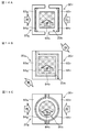
- FIG. 3A shows a plan view of the pixel structure according to Example 1
- FIG. 3B shows a cross-sectional view along the line AA in FIG. 3A.
- the organic EL element 21 and its drive circuit are formed on a semiconductor substrate such as a silicon substrate.
- a circuit layer on which a driving circuit is formed is stacked on a semiconductor substrate, and an interlayer insulating film 81 shown in FIG. 3B is formed on the circuit layer.
- a pixel is formed on the interlayer insulating film 81. 20 will be formed. That is, the upper surface of the interlayer insulating film 81 becomes a pixel formation surface, and the pixels 20 are formed on the pixel formation surface.
- a plurality of concave portions 82 corresponding to the number of pixels 20 are provided on the upper surface of the interlayer insulating film 81 that is a pixel formation surface, and each of the plurality of concave portions 82 has four colors of RGBW.
- the pixel 20 composed of the sub-pixels 20r, 20g, 20b, and 20w is arranged. That is, the pixel structure according to the first embodiment is a three-dimensional arrangement structure in which the pixels 20 including the RGBW four-color sub-pixels 20r, 20g, 20b, and 20w are arranged in each of the plurality of concave portions 82.
- the plurality of recesses 82 have, for example, a substantially circular shape in plan view and are divided into three parts in the circumferential direction.
- the side wall (side surface) of the recess 82 is a vertical surface perpendicular to the pixel formation surface.
- the “vertical surface” includes not only a strictly vertical surface but also a substantially vertical surface, and the existence of various variations in design or manufacturing is allowed. However, it does not necessarily have to be a vertical surface, and may be an inclined surface that is inclined in the direction in which the opening of the recess 82 widens.
- the pixel 20 including the RGBW sub-pixels 20r, 20g, 20b, and 20w can be arranged in one recess 82. I have to. Specifically, each of the organic EL elements 21 of the RGB sub-pixels 20r, 20g, and 20b is formed on a side wall that is divided into three portions of the recess 82, and the organic EL element 21 of the W sub-pixel 20w is the bottom surface of the recess 82. Is formed.
- FIG. 3B shows a cross-sectional structure of the G sub-pixel 20g, the R sub-pixel 20r, and the W sub-pixel 20w.
- the anode electrodes 83g and 83r of the sub-pixels 20g and 20r are embedded as side anode electrodes in the side wall of the recess 82, and the anode electrode 83w of the sub-pixel 20w is embedded as a bottom anode electrode on the bottom surface of the recess 82.
- a metal material such as aluminum (Al) or a laminate of ITO (Indium Tin Oxide) and silver (Ag) can be used.
- an organic EL material that is a light emitting material is formed on the side anode electrode by oblique vapor deposition.
- the arrows shown in FIG. 3A indicate the film forming directions by oblique deposition of RGB.
- the organic EL material of each color is formed in the order of G ⁇ R ⁇ B.
- a G organic EL layer 84g is formed on the G anode electrode 83g by oblique deposition. As a result, the G sub-pixel 20g is formed. At this time, in oblique vapor deposition, by setting the incident angle of the organic EL material, which is a light emitting material, to an optimum angle, the G organic EL layer 84g is also applied to the W anode electrode 83w on the bottom surface of the recess 82. A film can be formed. Details of the incident angle of the organic EL material will be described later.
- the R organic EL layer 84r is formed on the R anode electrode 83r by oblique deposition. As a result, the R sub-pixel 20r is formed. At this time, by the oblique deposition, the R organic EL layer 84r is formed on the G organic EL layer 84g formed on the bottom surface of the recess 82.
- the B organic EL layer 84b is formed on the B anode electrode 83b by oblique vapor deposition. As a result, the B sub-pixel 20b is formed. At this time, by the oblique deposition, the B organic EL layer 84 b is formed on the R organic EL layer 84 r formed on the bottom surface of the recess 82.
- the G organic EL layer 84g, the R organic EL layer 84r, and the B organic EL layer are formed on the W anode electrode 83w on the bottom surface of the recess 82.
- 84b is laminated.
- a W sub-pixel 20w including a stack of the G organic EL layer 84g, the R organic EL layer 84r, and the B organic EL layer 84b is formed on the bottom surface of the recess 82.
- a cathode electrode 85 made of a transparent electrode is formed as a common electrode for all the pixels 20 on the G organic EL layer 84g, the R organic EL layer 84r, and the B organic EL layer 84b. Is done.
- a material such as ITO, IZO (Indium Zink Oxide), ZnO (zinc oxide) or the like can be used as the material of the cathode electrode 85.
- a protective film 86 is formed on the cathode electrode 85.
- the pixels 20 including the RGBW sub-pixels 20r, 20g, 20b, and 20w are three-dimensionally arranged in each of the plurality of recesses 82 formed on the pixel formation surface. It has a pixel structure.
- the size of the bottom surface of the recess 82 where the W sub-pixel 20w is formed corresponds to the size of one sub-pixel when the RGBW sub-pixels 20r, 20g, 20b, and 20w are arranged in a plane. .
- the RGBW sub-pixels 20r, 20g, 20b, and 20w are subdivided into the size of the sub-pixels by the three-dimensional arrangement of the pixels 20 using the side wall and the bottom surface (bottom) of the recess 82. Therefore, even with the separate coloring method, high definition can be achieved.
- FIG. 4A shows a state of light emission from the G sub-pixel 20g
- FIG. 4B shows a state of light emission from the W sub-pixel 20w.
- the organic EL layers 84g, 84r, and 84b of each color are formed by oblique deposition, for example, in the order of G ⁇ R ⁇ B.
- the organic EL layers 84g, 84r, and 84b of the respective colors are sequentially formed on the bottom surface of the concave portion 82.
- the RGB sub-pixels 20r, 20g, and 20b are sequentially formed, and at the same time, the W sub-pixel 20w is formed by stacking the G organic EL layer 84g, the R organic EL layer 84r, and the B organic EL layer 84b.
- the W sub-pixel 20w is formed by stacking the G organic EL layer 84g, the R organic EL layer 84r, and the B organic EL layer 84b.
- the incident angle during oblique deposition is the width x of the bottom anode electrode (W anode electrode 83w) and the side anode electrode (for example, G anode electrode 83g).
- the incident limit angle that is, the maximum incident angle ⁇ max and the minimum incident angle ⁇ min are set based on the size y in the depth direction.
- Example 2 is a modification of Example 1 and is another example of the shape of the recess 82.
- FIG. 6 shows a plan view of a pixel structure according to the second embodiment.
- the concave portion 82 has a substantially circular shape in plan view and is divided into three in the circumferential direction.
- the recess 82 has a substantially triangular plan view shape.
- the RGB sub-pixels 20r, 20g, and 20b are formed on the side walls corresponding to the sides of the triangle, and the W sub-pixel 20w is formed on the bottom surface.
- the formation of the RGBW sub-pixels 20r, 20g, 20b, and 20w can be performed by oblique vapor deposition in the same manner as in the first embodiment. In FIG. 6, the film forming directions by oblique vapor deposition of RGB are indicated by arrows.
- the third embodiment is an example of a manufacturing method of the pixel structure according to the first embodiment, that is, the pixel structure in which the pixel 20 is composed of four sub-pixels 20r, 20g, 20b, and 20w of RGBW.
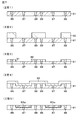
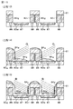
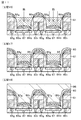
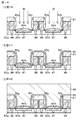
- Process diagrams of a method for manufacturing a pixel structure according to Example 3 are shown in FIGS. 7, 8, 9, 10, and 11.
- the oblique deposition is used for the film formation of the organic EL material of the RGBW sub-pixels 20r, 20g, 20b, and 20w.
- a wiring line made of aluminum (Al) or copper (Cu) and an anode electrode 83w as a bottom anode electrode and anode electrodes 83r, 83g, and 83b as side anode electrodes are electrically connected to the underlying interlayer insulating film 81.
- a contact plug 87 and a contact plug 88 are formed (step 1). Examples of the material of the interlayer insulating film 81 include SiO, SiON, SiN, and SiOC. Examples of the material of the contact plug 87 and the contact plug 88 include tungsten (W).
- one pixel is composed of three RGB sub-pixels 20r, 20g, and 20b, but in this embodiment, it is composed of four RGBW sub-pixels 20r, 20g, 20b, and 20w.
- the size per pixel is, for example, about 1 to 30 ⁇ m.
- a photoresist 90 for i-line or KrF is formed on the underlying interlayer insulating film 81. Patterning, exposure, and development are performed to open only the position of the W anode electrode 83w (step 2).
- the interlayer insulating film 81 is processed by, for example, 5 nm or more using an F-based etching gas to form a recess 89 (step 3).
- the film thickness of the W anode electrode 83w can be formed more uniformly.
- O2 ashing and cleaning are performed.
- an electrode forming layer 92 for forming a W anode electrode 83w is formed in the recess 89 on the interlayer insulating film 81 over the entire surface of the interlayer insulating film 81 (step 4).
- the electrode forming layer 92 to be the W anode electrode 83w is made of, for example, a laminate of titanium (Ti) and aluminum (Al).
- Ti is formed to a thickness of about 1 to 500 nm and Al is formed to a thickness of about 10 to 1 ⁇ m and stacked.
- the electrode forming layer 92 on the interlayer insulating film 81 outside the recess 89 is shaved by CMP (Chemical Mechanical Polishing) or etch back to form a W anode electrode 83w (Step 5).
- CMP Chemical Mechanical Polishing
- overetching is performed until the contact plug 88 for the side anode electrode is completely exposed on the surface of the interlayer insulating film 81.
- electrode formation for forming side anode electrodes that is, RGB anode electrodes 83r, 83g, and 83b, on the W anode electrode 83w and the contact plug 88 for the side anode electrode exposed by CMP or etch back is performed.
- Layer 93 is formed (step 6). At this time, the electrode forming layer 93 is formed so that the film thickness ratio with respect to the maximum size of the bottom anode electrode is in the range of 0.5 to 2, for example.
- Examples of the material of the electrode forming layer 93 to be the RGB anode electrodes 83r, 83g, and 83b include Al.
- an i-line or KrF photoresist 94 is formed on the electrode formation layer 93, exposed and developed to form a bottom anode electrode opening 95, and a processing mask for side anode electrode separation. Form (step 7).
- step 8 by etching the electrode forming layer 93 with a Cl-based gas, the surface of the W anode electrode 83w that is the bottom anode electrode and the formation of the RGB anode electrodes 83r, 83g, and 83b that are the side anode electrodes are formed. Perform (step 8).
- the photoresist 94 is removed by O2 ashing, and then the residue is removed by washing (step 9).
- the formed bottom anode electrode and side anode electrode are backfilled with the interlayer insulating film 81 (step 10).
- the film thickness of the interlayer insulating film 81 is made larger than the height of the side anode electrode.
- a photoresist 96 is applied for opening the bottom anode electrode and the side anode electrode, and the photoresist 96 is patterned by exposure and development to form an opening 97 for the bottom anode electrode and the side anode electrode (step 11). ).
- etch back is performed through the opening 97 of the photoresist 96 until the bottom anode electrode is exposed (step 12). At this time, a processing end point is detected based on a signal resulting from the interlayer insulating film 81.
- the photoresist 96 is removed by O2 ashing, and then the residue is removed by washing (step 13).
- the G organic EL material 84g is obliquely deposited toward the G anode electrode 83g to form the G organic EL layer 84g (step 14).
- a G organic EL material is deposited on the W anode electrode 83 w on the bottom surface of the recess 82.
- the incident angle ⁇ of the organic EL material (light emitting material) with respect to the bottom surface of the recess 82 by adjusting the relative position between the substrate and the evaporation source of the organic EL material.
- the incident angle ⁇ of the organic EL material is set to an optimum angle, when the G organic EL material is obliquely deposited, the organic G material is also formed on the W anode electrode 83w on the bottom surface of the recess 82.
- An EL material can be deposited.
- the incident angle ⁇ referred to here is the incident limit angle described in FIG. 5, that is, the maximum incident angle ⁇ max and the minimum incident angle ⁇ min .
- an R organic EL layer 84r is formed by oblique vapor deposition of an R organic EL material toward the R anode electrode 83r (step 15). At the same time, an R organic EL material is deposited on the W anode electrode 83 w on the bottom surface of the recess 82.
- the B organic EL layer 84b is formed by oblique deposition of the B organic EL material toward the B anode electrode 83b (step 16).
- the organic EL material is deposited on the W anode electrode 83 w at the bottom of the recess 82.
- a film of GRB is deposited on the W anode electrode 83w.
- a cathode electrode 85 made of a transparent electrode is formed with a film thickness of, for example, 5 nm to 5 ⁇ m by sputtering (step 17).
- the cathode electrode 85 made of a transparent electrode can also be used as a protective film by forming a thick film.
- the material of the cathode electrode 85 include ITO (indium tin oxide) and IZO (indium zinc oxide).
- a specific alloy for example, Mg, Ag, etc. can be formed as a thin film to form the cathode electrode 85.
- a protective layer 86 is formed (step 18).
- the protective layer 86 it is preferable to form a film of SiN, SiON, organic resin or the like having a high protective performance in a single layer or a laminated structure.
- the total film thickness of the protective layer 86 is, for example, about 0.3 ⁇ m to 10 ⁇ m.
- Al it is possible to use Al as a protective film, in this case, the bottom anode electrode is formed using a transparent film such as ITO.
- the organic EL materials of the respective colors can be formed on the sidewalls of the recesses 82 by oblique deposition, for example, in the order of G ⁇ R ⁇ B. .
- the organic EL materials of these colors are formed, the organic EL materials of the respective colors are sequentially formed and stacked on the bottom surface of the recess 82, so that the RGB sub-pixels 20r, 20g, and 20b are sequentially formed.
- the W sub-pixel 20w can be formed.
- the organic EL material of each color is formed on the side wall of the recess 82 in the order of G ⁇ R ⁇ B.
- the organic EL layers 84g, 84r, and 84b can be formed.
- the fourth embodiment is an example in which the pixel 20 includes RGB sub-pixels 20r, 20g, and 20b.
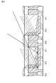
- FIG. 12A shows a plan view of the pixel structure according to Example 4, and
- FIG. 12B shows an end view of the cut portion along the line BB in FIG. 12A.
- the organic EL element 21 and its drive circuit are formed on a semiconductor substrate such as a silicon substrate.
- a plurality of concave portions 82 corresponding to the number of pixels 20 are provided on the upper surface of the interlayer insulating film 81 that is a pixel formation surface, and three colors of RGB are provided in each of the plurality of concave portions 82.
- the pixel 20 composed of the sub-pixels 20r, 20g, and 20b is arranged. That is, the pixel structure according to the fourth embodiment is a three-dimensional arrangement structure in which the pixels 20 including the RGB sub-pixels 20r, 20g, and 20b are arranged in each of the plurality of concave portions 82.
- the plurality of recesses 82 have, for example, a substantially circular shape in plan view and are divided into two in the circumferential direction.
- the side wall of the recess 82 is illustrated as a vertical plane perpendicular to the pixel formation surface.
- the side wall is not necessarily a vertical plane, and is an inclined plane inclined in the direction in which the opening of the recess 82 spreads. There may be.
- the pixel 20 including the RGB sub-pixels 20r, 20g, and 20b can be arranged in one recess 82. Yes. Specifically, each of the organic EL elements 21 of the RG sub-pixels 20r and 20g is formed on the two-divided sidewalls of the recess 82, and the organic EL element 21 of the B sub-pixel 20b is formed on the bottom surface of the recess 82. Has been.
- FIG. 12B shows a cross-sectional structure of the G sub-pixel 20g, the R sub-pixel 20r, and the B sub-pixel 20b.
- the anode electrodes 83g and 83r of the sub-pixels 20g and 20r are embedded as side anode electrodes in the sidewall of the recess 82, and the anode electrode 83b of the sub-pixel 20b is embedded as a bottom anode electrode in the bottom surface of the recess 82.
- the anode electrodes 83g and 83r which are side anode electrodes have a substantially semicircular shape in plan view.
- the material for the anode electrode is the same as in the first embodiment.
- an organic EL layer that is a light emitting layer is formed on the side anode electrode by oblique vapor deposition.
- the arrows shown in FIG. 12A indicate the film forming directions of RGB.
- the film forming direction of B is a direction perpendicular to the bottom surface of the recess 82.
- the organic EL layers of the respective colors are formed in the order of G ⁇ R ⁇ B.
- a G organic EL layer 84g is formed on the G anode electrode 83g by oblique deposition.
- vapor deposition is performed so that a G organic EL material is formed on the sidewall of the recess 82.
- the R organic EL layer 84r is formed on the R anode electrode 83r by oblique deposition. Also in this case, vapor deposition is performed so that the R organic EL material is formed on the sidewall of the recess 82.
- the B organic EL layer 84g is formed on the B anode electrode 83b provided on the bottom surface of the recess 82.
- the pixel structure according to the fourth embodiment has a pixel structure in which the pixels 20 including the RGB sub-pixels 20r, 20g, and 20b are three-dimensionally arranged in each of the plurality of recesses 82 formed on the pixel formation surface. It has become.
- the size of the bottom surface of the recess 82 in which the B sub-pixel 20b is formed corresponds to the size of one sub-pixel when the RGB sub-pixels 20r, 20g, and 20b are arranged in a plane.
- the pixel 20 including the RGB sub-pixels 20r, 20g, and 20b is formed in the size of the sub-pixel by the three-dimensional arrangement of the pixels 20 using the side wall and the bottom surface of the recess 82. Since it can be arranged, high-definition can be achieved even with the separate painting method.
- the electrodes of the anode electrodes of other colors Since the light is reflected off the surface and emitted out of the recess 82, the light extraction efficiency can be increased and the viewing angle dependency does not occur.
- FIG. 13 shows a state of light emission from the B sub-pixel 20b provided on the bottom surface of the recess 82.
- FIG. 13 shows a state of light emission from the B sub-pixel 20b provided on the bottom surface of the recess 82.
- light emitted on the anode electrode 83b of the B sub-pixel 20b is reflected on the electrode surface of the anode electrode 83r of the R sub-pixel 20r and the electrode surface of the anode electrode 83g of the G sub-pixel 20g.
- the state of being emitted out of the recess 82 is shown.
- the fifth embodiment is a modification of the fourth embodiment and is another example of the shape of the anode electrodes 83g and 83r as the side anode electrodes.
- Plan views of the pixel structure according to Example 5 are shown in FIGS. 14A, 14B, and 14C.
- the film formation direction of the organic EL material is indicated by an arrow.
- the image structure according to Example 4 has a configuration in which the shape of the anode electrodes 83g and 83r of the GR is substantially semicircular, and the anode electrodes 83g and 83r are arranged to face each other.
- the anode electrodes 83g and 83r of the GR have the planar view shapes shown in FIGS. 14A, 14B, and 14C.
- the planar shape of the anode electrodes 83g and 83r of the GR is substantially U-shaped, and the substantially U-shaped anode electrodes 83g and 83r are opposed to each other and arranged in a rectangular shape.
- GR organic EL layers 84g and 84r are formed on the inner surfaces of the anode electrodes 83g and 83r.
- the plan view shape of the B organic EL layer 84b formed on the bottom surface of the recess 82 is rectangular.
- the planar shape of the anode electrodes 83g and 83r of the GR is substantially L-shaped, and the substantially L-shaped anode electrodes 83g and 83r are arranged in a rectangular shape so as to be opposite to each other.
- the organic EL layers 84g and 84r of GR are formed on the substantially L-shaped inner surface of 83r.
- the plan view shape of the B organic EL layer 84b formed on the bottom surface of the recess 82 is rectangular.
- the shape of the inner surfaces of the GR anode electrodes 83g and 83r in a plan view is substantially semicircular, and the anode electrodes 83g and 83r whose inner surfaces are substantially semicircular are arranged to face each other.
- the organic EL layers 84g and 84r of GR are formed on the substantially semicircular inner surface of 83r.
- the plan view shape of the B organic EL layer 84b formed on the bottom surface of the recess 82 is circular.
- the sixth embodiment is an example of a manufacturing method of the pixel structure according to the fourth embodiment, that is, the pixel structure in which the pixel 20 is composed of RGB sub-pixels 20r, 20g, and 20b.
- Process diagrams of a method for manufacturing a pixel structure according to Example 6 are shown in FIGS. Oblique vapor deposition is used to form the organic EL material of the RG sub-pixels 20r and 20g.
- Processes from Step 1 to Step 13 are the same as those from Step 1 to Step 13 in the third embodiment.
- the pixel 20 has a pixel structure including three sub-pixels 20r, 20g, and 20b of RGB
- the anode electrode 83w of W in the third embodiment is used as the anode electrode on the bottom surface of the recess 82.
- the anode electrode 83b is replaced.
- Etchback is performed until the B anode electrode 83b which is the bottom anode electrode is exposed, and then G organic EL material is obliquely deposited toward the G anode electrode 83g of the two anode electrodes on the side surface of the recess 82. Thereby, a G organic EL layer 84g is formed (step 14).
- the substrate of the organic EL material is adjusted by the relative position adjustment between the substrate and the evaporation source of the organic EL material so that the G organic EL material is not formed on the B anode electrode 83b on the bottom surface of the recess 82. It is necessary to control the incident angle ⁇ with respect to.
- an R organic EL layer 84r is formed by oblique vapor deposition of an R organic EL material toward the R anode electrode 83r (step 15). Similarly, it is necessary to control the incident angle ⁇ of the organic EL material with respect to the substrate so that the R organic EL material is not formed on the B anode electrode 83 b on the bottom surface of the recess 82.
- a B organic EL layer 84b is formed by depositing a B organic EL material on the B anode electrode 83b on the bottom surface of the recess 82 (step 16).
- the G organic EL layer 84g and the R organic EL layer 84r are formed on the sidewall of the recess 82, and the B organic EL layer 84b is formed on the bottom surface of the recess 82. Is done.
- a cathode electrode 85 made of a transparent electrode is formed with a film thickness of, for example, 5 nm to 5 ⁇ m by sputtering (step 17).
- the cathode electrode 85 made of a transparent electrode can also be used as a protective film by forming a thick film.
- the material of the cathode electrode 85 and the like are the same as in the case of the third embodiment.
- a protective layer 86 is formed (step 18).
- the material for the protective layer 86 and the like are the same as those in the third embodiment.
- the G sub-pixel 20g and the R sub-pixel 20r are formed on the side wall of the recess 82, and the B sub-pixel 20b is formed on the bottom surface of the recess 82. It is not limited to this. That is, a pixel structure in which the G sub-pixel 20 g or the R sub-pixel 20 r is formed on the bottom surface of the recess 82 may be employed.
- the display device of the present disclosure described above is a display unit (display device) of an electronic device in any field that displays a video signal input to the electronic device or a video signal generated in the electronic device as an image or a video.
- the electronic device include a television set, a notebook personal computer, a digital still camera, a mobile terminal device such as a mobile phone, a head mounted display, and the like. However, it is not restricted to these.
- the following effects can be obtained by using the display device of the present disclosure as the display unit in electronic devices of various fields. That is, according to the display device of the present disclosure, high-definition can be achieved by a separate coloring method, light extraction efficiency can be increased, and viewing angle dependence does not occur. Therefore, by using the display device of the present disclosure, it is possible to contribute to high definition and high image quality of the display unit of the electronic device.
- the display device of the present disclosure also includes a module-shaped one with a sealed configuration.
- a display module formed by attaching a facing portion such as transparent glass to the pixel array portion is applicable.
- the display module may be provided with a circuit unit for inputting / outputting signals from the outside to the pixel array unit, a flexible printed circuit (FPC), and the like.
- FPC flexible printed circuit
- a digital still camera and a head mounted display will be exemplified as specific examples of the electronic apparatus using the display device of the present disclosure.
- the specific example illustrated here is only an example, and is not limited thereto.
- FIG. 17A and 17B are external views of an interchangeable-lens single-lens reflex digital still camera according to Specific Example 1 of the electronic apparatus of the present disclosure.
- FIG. 17A shows a front view thereof
- FIG. 17B shows a rear view thereof.
- the interchangeable-lens single-lens reflex digital still camera includes, for example, an interchangeable photographing lens unit (interchangeable lens) 212 on the front right side of the camera body (camera body) 211, and the front left side.
- the camera has a grip part 213 for the photographer to hold.
- a monitor 214 is provided in the approximate center of the back of the camera body 211.
- An electronic viewfinder (eyepiece window) 215 is provided on the monitor 214. The photographer can look into the electronic viewfinder 215 and visually determine the subject's optical image guided from the photographing lens unit 212 to determine the composition.
- the display device of the present disclosure can be used as the electronic viewfinder 215. That is, the interchangeable lens single-lens reflex digital still camera according to the first specific example is manufactured by using the display device of the present disclosure as the electronic viewfinder 215.
- FIG. 18 is an external view illustrating an example of a head-mounted display according to the specific example 2 of the electronic apparatus of the present disclosure.
- the head mounted display 300 has a transmissive head mounted display configuration including a main body portion 301, an arm portion 302, and a lens barrel 303.
- the main body 301 is connected to the arm 302 and the glasses 310. Specifically, the end of the main body 301 in the long side direction is attached to the arm 302. Further, one side of the side surface of the main body 301 is connected to the glasses 310 via a connection member (not shown).
- the main body 301 may be directly attached to the head of a human body.
- the main body unit 301 includes a control board and a display unit for controlling the operation of the head mounted display 300.
- the arm portion 302 supports the lens barrel 303 with respect to the main body portion 301 by connecting the main body portion 301 and the lens barrel 303. Specifically, the arm portion 302 is coupled to the end portion of the main body portion 301 and the end portion of the lens barrel 303, thereby fixing the lens barrel 303 to the main body portion 301.
- the arm unit 302 includes a signal line for communicating data related to an image provided from the main body unit 301 to the lens barrel 303.
- the lens barrel 303 projects image light provided from the main body 301 via the arm unit 302 through the lens 311 of the glasses 310 toward the eyes of the user wearing the head mounted display 300.
- the display device of the present disclosure can be used as a display unit built in the main body unit 301. That is, the head mounted display 300 according to the second specific example is manufactured by using the display device of the present disclosure as the display unit.
- this indication can also take the following structures.
- Display device >> [A-1] a plurality of recesses provided on the pixel formation surface, and A pixel disposed in each of the plurality of recesses, The light emitting portion of the pixel is formed on each side wall and bottom surface of the plurality of recesses. Display device. [A-2] The pixel has a plurality of light emitting portions having different light emission colors, One of the plurality of light emitting portions is formed on the bottom surface of each of the plurality of recesses, The display device according to [A-1].
- the emission colors of the plurality of light emitting units are composed of four colors of red, green, blue, and white,
- the red, green, and blue light emitting portions are formed on the side walls of the plurality of recesses,
- the white light emitting part is formed on the bottom surface of each of the plurality of recesses.
- [A-4] The light emitting layer of the light emitting part formed on the side wall of the recess is formed by oblique vapor deposition of a light emitting material on the side wall of the recess.
- the incident angle of the luminescent material with respect to the bottom surface of the recess is set to an angle for forming a luminescent layer on the side wall and bottom surface of the recess.
- [A-6] The incident angle of the luminescent material is set based on the size of the side anode electrode formed on the side wall of the recess and the size of the bottom anode electrode formed on the bottom surface of the recess.
- the light emission colors of the plurality of light emitting units are composed of two colors, red, green, and blue, The light emitting part of two colors of the three colors is formed on each side wall of the plurality of recesses, The remaining one color light emitting part is formed on the bottom surface of each of the plurality of recesses.
- [A-8] The light emitting layer of the light emitting part formed on the side wall of the recess is formed by oblique vapor deposition of a light emitting material on the side wall of the recess.
- the incident angle of the light emitting material with respect to the bottom surface of the recess is set to an angle at which the light emitting layer is not formed on the bottom surface of the recess.
- the light-emitting portion of the pixel is composed of an organic electroluminescence element.
- the emission colors of the plurality of light emitting units are composed of four colors of red, green, blue, and white, Forming red, green, and blue light emitting portions on each side wall of the plurality of recesses; Forming a white light emitting part on the bottom surface of each of the plurality of recesses; The method for manufacturing a display device according to [B-2] above.
- a light emitting layer of the light emitting portion formed on the side wall of the concave portion is formed by oblique vapor deposition of a light emitting material on the side wall of the concave portion. The method for manufacturing a display device according to [B-3] above.
- the incident angle of the luminescent material with respect to the bottom surface of the recess is set to an angle at which a luminescent layer is formed on the side wall and the bottom surface of the recess.
- the incident angle of the luminescent material is set based on the size of the side anode electrode formed on the side wall of the recess and the size of the bottom anode electrode formed on the bottom surface of the recess.
- the emission colors of the plurality of light emitting units are composed of two colors, red, green, and blue, A light emitting portion of two colors of the three colors is formed on each side wall of the plurality of recesses, Forming the remaining one color light emitting portion on the bottom surface of each of the plurality of recesses;
- a light emitting layer of the light emitting part formed on the side wall of the recess is formed by oblique vapor deposition of a light emitting material on the side wall of the recess.
- the incident angle of the light emitting material with respect to the bottom surface of the recess is set to an angle at which the light emitting layer is not formed on the bottom surface of the recess.
- the light-emitting portion of the pixel is composed of an organic electroluminescence element.
- the emission colors of the plurality of light emitting units are composed of four colors of red, green, blue, and white,
- the red, green, and blue light emitting portions are formed on the side walls of the plurality of recesses,
- the white light emitting part is formed on the bottom surface of each of the plurality of recesses.
- [C-4] The light emitting layer of the light emitting part formed on the side wall of the concave portion is formed by oblique deposition of the light emitting material on the side wall of the concave portion.
- the incident angle of the luminescent material with respect to the bottom surface of the recess is set to an angle for forming a luminescent layer on the side wall and the bottom surface of the recess.
- [C-6] The incident angle of the luminescent material is set based on the size of the side anode electrode formed on the side wall of the recess and the size of the bottom anode electrode formed on the bottom surface of the recess.
- the light emission colors of the plurality of light emitting units are composed of two colors of red, green, and blue, The light emitting part of two colors of the three colors is formed on each side wall of the plurality of recesses, The remaining one color light emitting part is formed on the bottom surface of each of the plurality of recesses.
- [C-8] The light emitting layer of the light emitting part formed on the side wall of the recess is formed by oblique vapor deposition of a light emitting material on the side wall of the recess.
- the incident angle of the light emitting material with respect to the bottom surface of the recess is set to an angle at which the light emitting layer is not formed on the bottom surface of the recess.
- [C-10] The light-emitting portion of the pixel is composed of an organic electroluminescence element.
Landscapes
- Engineering & Computer Science (AREA)
- Manufacturing & Machinery (AREA)
- Physics & Mathematics (AREA)
- General Physics & Mathematics (AREA)
- Theoretical Computer Science (AREA)
- Microelectronics & Electronic Packaging (AREA)
- Optics & Photonics (AREA)
- Electroluminescent Light Sources (AREA)
- Devices For Indicating Variable Information By Combining Individual Elements (AREA)
Abstract
本開示の表示装置は、画素形成面に設けられた複数の凹部、及び、複数の凹部の各々に配された画素を備えており、画素の発光部は、複数の凹部の各々の側壁及び底面に形成されている。本開示の表示装置の製造方法は、上記の構成の表示装置についての製造方法である。また、本開示の電子機器は、上記の構成の表示装置を有する電子機器である。
Description
本開示は、表示装置及び表示装置の製造方法、並びに、電子機器に関する。
近年の表示装置は、平面型(フラットパネル型)の表示装置が主流である。平面型の表示装置の一つとして、デバイスに流れる電流値に応じて発光輝度が変化する、所謂、電流駆動型の電気光学素子を、画素の発光部(発光素子)として用いた表示装置がある。電流駆動型の電気光学素子としては、有機材料のエレクトロルミネッセンス(EL:Electro Luminescence)を利用し、有機薄膜に電界をかけると発光する現象を用いた有機EL素子が知られている。
有機EL素子は、アノード電極上に有機EL材料を蒸着成膜することによって形成される。また、カラー表示を実現する方式の一つとして、R(赤)G(緑)B(青)の各色の素子を個別にパターニングする塗り分け方式がある。この塗り分け方式の場合、RGBの各色毎に他の色の電極開口部をマスキングして有機EL材料を蒸着する必要がある。このため、マスクの位置合わせ精度が画素ピッチを制限してしまうことになる。このマスク精度の観点から高精細化が難しく、画素ピッチが小さくなる程、この傾向は顕著である。
ところで、従来の画素配列では、RGBの各色の素子は、バックプレーン基板の基板面に対して平行な平坦面に形成されるのが一般的であった。これに対し、基板上に複数の多面構造体を形成し、当該多面構造体の傾斜面上に発光素子を形成し、画素をストライプ配列した発光装置が提案されている(例えば、特許文献1参照)。
上記の特許文献1に記載の従来技術において、発光素子が形成される傾斜面を有する多面構造体は、基板上に突出した状態で形成された突起部である。基板上の突起部である多面構造体の傾斜面上に発光素子を形成した従来技術の場合、各色の発光素子からは、画素の中心から離れる方向、即ち拡散する方向に光が発せられることになるため、光の取り出し効率の低下や視野角依存が生じる。
本開示は、塗り分け方式にて高精細化を可能にするとともに、光の取り出し効率を高めることができる表示装置及び表示装置の製造方法、並びに、当該表示装置を有する電子機器を提供することを目的とする。
上記の目的を達成するための本開示の表示装置は、
画素形成面に設けられた複数の凹部、及び、
複数の凹部の各々に配された画素を備えており、
画素の発光部は、複数の凹部の各々の側壁及び底面に形成されている。
画素形成面に設けられた複数の凹部、及び、
複数の凹部の各々に配された画素を備えており、
画素の発光部は、複数の凹部の各々の側壁及び底面に形成されている。
また、上記の目的を達成するための本開示の表示装置の製造方法は、
画素形成面に設けられた複数の凹部、及び、
複数の凹部の各々に配された画素を備える表示装置の製造に当たって、
複数の凹部の各々の側壁及び底面に画素の発光部を形成する。
画素形成面に設けられた複数の凹部、及び、
複数の凹部の各々に配された画素を備える表示装置の製造に当たって、
複数の凹部の各々の側壁及び底面に画素の発光部を形成する。
また、上記の目的を達成するための本開示の電子機器は、上記の構成の表示装置を有する。
以下、本開示の技術を実施するための形態(以下、「実施形態」と記述する)について図面を用いて詳細に説明する。本開示の技術は実施形態に限定されるものではなく、実施形態における種々の数値や材料などは例示である。以下の説明において、同一要素又は同一機能を有する要素には同一符号を用いることとし、重複する説明は省略する。尚、説明は以下の順序で行う。
1.本開示の表示装置及びその製造方法、並びに、電子機器、全般に関する説明
2.本開示の技術が適用される表示装置
2-1.システム構成
2-2.画素回路
2-3.塗り分け方式について
3.本開示の実施形態
3-1.実施例1(画素がRGBWの4色のサブ画素から成る例)
3-2.実施例2(実施例1の変形例:凹部の形状の他の例)
3-3.実施例3(実施例1に係る画素構造の製造方法の例)
3-4.実施例4(画素がRGBの3色のサブ画素から成る例)
3-5.実施例5(実施例4の変形例:サイドアノード電極の形状の他の例)
3-6.実施例6(実施例4に係る画素構造の製造方法の例)
4.変形例
5.本開示の電子機器
5-1.具体例1(デジタルスチルカメラの例)
5-2.具体例2(ヘッドマウントディスプレイの例)
6.本開示がとることができる構成
1.本開示の表示装置及びその製造方法、並びに、電子機器、全般に関する説明
2.本開示の技術が適用される表示装置
2-1.システム構成
2-2.画素回路
2-3.塗り分け方式について
3.本開示の実施形態
3-1.実施例1(画素がRGBWの4色のサブ画素から成る例)
3-2.実施例2(実施例1の変形例:凹部の形状の他の例)
3-3.実施例3(実施例1に係る画素構造の製造方法の例)
3-4.実施例4(画素がRGBの3色のサブ画素から成る例)
3-5.実施例5(実施例4の変形例:サイドアノード電極の形状の他の例)
3-6.実施例6(実施例4に係る画素構造の製造方法の例)
4.変形例
5.本開示の電子機器
5-1.具体例1(デジタルスチルカメラの例)
5-2.具体例2(ヘッドマウントディスプレイの例)
6.本開示がとることができる構成
<本開示の表示装置及びその製造方法、並びに、電子機器、全般に関する説明>
本開示の表示装置及びその製造方法、並びに、電子機器にあっては、画素について、互いに発光色が異なる複数の発光部を有する構成とすることができる。そして、複数の発光部の一つは、複数の凹部の各々の底面に形成されている構成とすることができる。
本開示の表示装置及びその製造方法、並びに、電子機器にあっては、画素について、互いに発光色が異なる複数の発光部を有する構成とすることができる。そして、複数の発光部の一つは、複数の凹部の各々の底面に形成されている構成とすることができる。
上述した好ましい構成を含む本開示の表示装置及びその製造方法、並びに、電子機器にあっては、複数の発光部の発光色が、赤色、緑色、青色、及び、白色の4色から成り、赤色、緑色、及び、青色の発光部が、複数の凹部の各々の側壁に形成され、白色の発光部が、複数の凹部の各々の底面に形成されている構成とすることができる。
更に、上述した好ましい構成を含む本開示の表示装置及びその製造方法、並びに、電子機器にあっては、凹部の側壁に形成される発光部の発光層について、凹部の側壁に対する発光材料の斜方蒸着によって成膜される構成とすることができる。そして、斜方蒸着において、凹部の底面に対する発光材料の入射角は、凹部の側壁及び底面に発光層を形成する角度に設定されることが好ましい。また、発光材料の入射角について、凹部の側壁に形成されるサイドアノード電極のサイズ、及び、凹部の底面に形成されるボトムアノード電極のサイズを基に設定される構成とすることができる。
あるいは又、上述した好ましい構成を含む本開示の表示装置及びその製造方法、並びに、電子機器にあっては、複数の発光部の発光色は、赤色、緑色、及び、青色の2色から成り、3色のうちの2色の発光部が、複数の凹部の各々の側壁に形成され、残りの1色の発光部が、複数の凹部の各々の底面に形成されている構成とすることができる。
更に、上述した好ましい構成を含む本開示の表示装置及びその製造方法、並びに、電子機器にあっては、凹部の側壁に形成される発光部の発光層について、凹部の側壁に対する発光材料の斜方蒸着によって成膜される構成とすることができる。そして、斜方蒸着において、凹部の底面に対する発光材料の入射角は、凹部の底面に発光層が形成されない角度に設定されることが好ましい。
更に、上述した好ましい構成を含む本開示の表示装置及びその製造方法、並びに、電子機器にあっては、画素の発光部について、有機エレクトロルミネッセンス素子から成る構成とすることができる。
<本開示の技術が適用される表示装置>
本開示の技術が適用される表示装置は、電気光学素子に流れる電流を、当該電気光学素子と同じ画素回路内に設けた能動素子、例えば絶縁ゲート型電界効果トランジスタによって制御するアクティブマトリクス型表示装置である。絶縁ゲート型電界効果トランジスタとしては、典型的には、MOS(Metal Oxide Semiconductor)トランジスタやTFT(Thin Film Transistor:薄膜トランジスタ)を例示することができる。
本開示の技術が適用される表示装置は、電気光学素子に流れる電流を、当該電気光学素子と同じ画素回路内に設けた能動素子、例えば絶縁ゲート型電界効果トランジスタによって制御するアクティブマトリクス型表示装置である。絶縁ゲート型電界効果トランジスタとしては、典型的には、MOS(Metal Oxide Semiconductor)トランジスタやTFT(Thin Film Transistor:薄膜トランジスタ)を例示することができる。
ここでは、一例として、デバイスに流れる電流値に応じて発光輝度が変化する電流駆動型の電気光学素子である例えば有機EL素子を、画素回路の発光部(発光素子)として用いるアクティブマトリクス型有機EL表示装置を例に挙げて説明するものとする。
[システム構成]
図1は、本開示の技術が適用される有機EL表示装置の構成の概略を示すシステム構成図である。図1に示すように、本適用例に係る有機EL表示装置10は、有機EL素子を含む複数の画素20が行列状に2次元配置されて成る画素アレイ部30、及び、当該画素アレイ部30の各画素20を駆動する周辺回路部を有する構成となっている。
図1は、本開示の技術が適用される有機EL表示装置の構成の概略を示すシステム構成図である。図1に示すように、本適用例に係る有機EL表示装置10は、有機EL素子を含む複数の画素20が行列状に2次元配置されて成る画素アレイ部30、及び、当該画素アレイ部30の各画素20を駆動する周辺回路部を有する構成となっている。
本適用例に係る有機EL表示装置10は、カラー表示対応の表示装置である。そして、画素20は、カラー画像を形成する単位となる主画素であり、互いに発光色が異なる複数のサブ画素から成る。一例として、画素20は、赤色(Red;R)光を発光するサブ画素20r、緑色(Green;G)光を発光するサブ画素20g、青色(Blue;B)光を発光するサブ画素20b、及び、白色(White;W)光を発光するサブ画素20wの4つのサブ画素から構成されている。
サブ画素20r,20g,20b,20wは、例えば格子状に配置されている。この格子状配置において、サブ画素20r,20g,20b,20wの各々の配列については、図1に示す色配列に限られるものではない。以下、サブ画素20r,20g,20b,20wを総称してサブ画素20sと記述する場合がある。
周辺回路部は、例えば、画素アレイ部30と同じ表示パネル70上に搭載された書込み走査部40、駆動走査部50、及び、信号出力部60等から成り、画素アレイ部30の各サブ画素20sを駆動する。尚、書込み走査部40、駆動走査部50、及び、信号出力部60のいくつか、あるいは全部を表示パネル70の外部に設ける構成を採ることも可能である。
表示パネル70の基板としては、ガラス基板等の絶縁性透明基板を用いることもできるし、シリコン基板等の半導体基板を用いることもできる。表示パネル70の基板として、シリコン基板等の半導体基板を用いた有機EL表示装置は、所謂、マイクロディスプレイ(小型ディスプレイ)と呼称され、デジタルスチルカメラの電子ビューファインダや、ヘッドマウントディスプレイの表示部等として用いて好適なものである。
画素アレイ部30には、m行n列のサブ画素20sの配列に対して、行方向(画素行の画素の配列方向/水平方向)に沿って走査線31(311~31m)及び駆動線32(321~32m)が画素行毎に配線されている。更に、m行n列のサブ画素20sの配列に対して、列方向(画素列の画素の配列方向/垂直方向)に沿って信号線33(331~33n)が画素列毎に配線されている。
走査線311~31mは、書込み走査部40の対応する行の出力端にそれぞれ接続されている。駆動線321~32mは、駆動走査部50の対応する行の出力端にそれぞれ接続されている。信号線331~33nは、信号出力部60の対応する列の出力端にそれぞれ接続されている。
書込み走査部40は、シフトレジスタ回路やアドレスデコーダ等によって構成されている。この書込み走査部40は、画素アレイ部30の各サブ画素20sへの映像信号の信号電圧の書込みに際して、走査線31(311~31m)に対して書込み走査信号WS(WS1~WSm)を順次供給することによって画素アレイ部30の各サブ画素20sを行単位で順番に走査する、所謂、線順次走査を行う。
駆動走査部50は、書込み走査部40と同様に、シフトレジスタ回路やアドレスデコーダ等によって構成されている。この駆動走査部50は、書込み走査部40による線順次走査に同期して、駆動線32(321~32m)に対して発光制御信号DS(DS1~DSm)を供給することによってサブ画素20sの発光/非発光(消光)の制御を行う。
信号出力部60は、信号供給源(図示せず)から供給される輝度情報に応じた映像信号の信号電圧(以下、単に「信号電圧」と記述する場合もある)Vsigと基準電圧Vofsとを選択的に出力する。ここで、基準電圧Vofsは、映像信号の信号電圧Vsigの基準となる電圧(例えば、映像信号の黒レベルに相当する電圧)に相当する電圧、あるいは、その近傍の電圧である。基準電圧Vofsは、補正動作を行う際に、初期化電圧として用いられる。
信号出力部60から択一的に出力される信号電圧Vsig/基準電圧Vofsは、信号線34(341~34n)を介して画素アレイ部30の各サブ画素20sに対して、書込み走査部40による線順次走査によって選択された画素行の単位で書き込まれる。すなわち、信号出力部60は、信号電圧Vsigを画素行(ライン)単位で書き込む線順次書込みの駆動形態を採っている。
[画素回路]
図2は、本開示の技術が適用される有機EL表示装置10における画素(画素回路)の回路構成の一例を示す回路図である。サブ画素20sの発光部は、有機EL素子21から成る。有機EL素子21は、デバイスに流れる電流値に応じて発光輝度が変化する電流駆動型の電気光学素子の一例である。
図2は、本開示の技術が適用される有機EL表示装置10における画素(画素回路)の回路構成の一例を示す回路図である。サブ画素20sの発光部は、有機EL素子21から成る。有機EL素子21は、デバイスに流れる電流値に応じて発光輝度が変化する電流駆動型の電気光学素子の一例である。
図2に示すように、サブ画素20sは、有機EL素子21と、有機EL素子21に電流を流すことによって当該有機EL素子21を駆動する駆動回路(画素駆動回路)とによって構成されている。有機EL素子21は、全てのサブ画素20sに対して共通に配線された共通電源線34にカソード電極が接続されている。図中、Celは、有機EL素子21の等価容量である。
有機EL素子21を駆動する駆動回路は、駆動トランジスタ22、サンプリングトランジスタ23、発光制御トランジスタ24、保持容量25、及び、補助容量26を有する構成となっている。ここでは、有機EL素子21及びその駆動回路を、ガラス基板のような絶縁体上ではなく、シリコン基板のような半導体基板上に形成することを想定し、駆動トランジスタ22として、Pチャネル型のトランジスタを用いる構成を採っている。
また、本例では、サンプリングトランジスタ23及び発光制御トランジスタ24についても、駆動トランジスタ22と同様に、Pチャネル型のトランジスタを用いる構成を採っている。従って、駆動トランジスタ22、サンプリングトランジスタ23、及び、発光制御トランジスタ24は、ソース/ゲート/ドレインの3端子ではなく、ソース/ゲート/ドレイン/バックゲートの4端子となっている。バックゲートには電源電圧Vddが印加される。
但し、サンプリングトランジスタ23及び発光制御トランジスタ24については、スイッチ素子として機能するスイッチングトランジスタであることから、Pチャネル型のトランジスタに限られるものではない。従って、サンプリングトランジスタ23及び発光制御トランジスタ24は、Nチャネル型のトランジスタでも、Pチャネル型とNチャネル型が混在した構成のものでもよい。
上記の構成のサブ画素20sにおいて、サンプリングトランジスタ23は、信号出力部60から信号線33を通して供給される映像信号の信号電圧Vsigをサンプリングすることによって保持容量25に書き込む。発光制御トランジスタ24は、電源電圧Vddのノードと駆動トランジスタ22のソース電極との間に接続され、発光制御信号DSによる駆動の下に、有機EL素子21の発光/非発光を制御する。
保持容量25は、駆動トランジスタ22のゲート電極とソース電極との間に接続されている。この保持容量25は、サンプリングトランジスタ23によるサンプリングによって書き込まれた映像信号の信号電圧Vsigを保持する。駆動トランジスタ22は、保持容量25の保持電圧に応じた駆動電流を有機EL素子21に流すことによって有機EL素子21を駆動する。
補助容量26は、駆動トランジスタ22のソース電極と、固定電位のノード、例えば、電源電圧Vddのノードとの間に接続されている。この補助容量26は、映像信号の信号電圧Vsigを書き込んだときに駆動トランジスタ22のソース電位が変動するのを抑制するとともに、駆動トランジスタ22のゲート-ソース間電圧Vgsを、駆動トランジスタ22の閾値電圧Vthにする作用を為す。
[塗り分け方式について]
上記の構成の有機EL表示装置10において、有機EL素子21は、カラー化の方式の一つである塗り分け方式にて、アノード電極上に発光材料である有機EL材料を蒸着成膜することによって形成されることになる。塗り分け方式は、サブ画素20s(20r,20g,20b,20w)の各色を塗り分け、各色の有機EL素子21をそれぞれ発光させることになるため、カラーフィルタを併用する方式に比べて、発光効率及び光の取り出し効率の観点からメリットが大きい方式である。
上記の構成の有機EL表示装置10において、有機EL素子21は、カラー化の方式の一つである塗り分け方式にて、アノード電極上に発光材料である有機EL材料を蒸着成膜することによって形成されることになる。塗り分け方式は、サブ画素20s(20r,20g,20b,20w)の各色を塗り分け、各色の有機EL素子21をそれぞれ発光させることになるため、カラーフィルタを併用する方式に比べて、発光効率及び光の取り出し効率の観点からメリットが大きい方式である。
但し、塗り分け方式の場合、サブ画素20sの各色毎に他の色の電極開口部をマスキングして有機EL材料を蒸着する必要があることから、マスクの位置合わせ精度が画素ピッチを制限してしまうことになるため、このマスク精度の観点から高精細化が難しく、画素ピッチが小さくなる程、この傾向は顕著である。
<本開示の実施形態>
そこで、本開示の実施形態では、塗り分け方式にて高精細化を可能にするために、画素形成面に複数の凹部を設け、これら複数の凹部の各々に画素20を配置した、所謂、画素20の立体的な配置構造を採っている。このとき、画素20の発光部である有機EL素子21については、複数の凹部の各々の側壁及び底面(底部)を利用して、サブ画素20s(20r,20g,20b,20w)毎に形成するようにする。ここでは、有機EL素子21の発光色について、RGBWの4色としたが、これに限られるものではなく、例えば、RGBの3色としてもよいし、高輝度化を目的として、全色を白色とすることも可能である。
そこで、本開示の実施形態では、塗り分け方式にて高精細化を可能にするために、画素形成面に複数の凹部を設け、これら複数の凹部の各々に画素20を配置した、所謂、画素20の立体的な配置構造を採っている。このとき、画素20の発光部である有機EL素子21については、複数の凹部の各々の側壁及び底面(底部)を利用して、サブ画素20s(20r,20g,20b,20w)毎に形成するようにする。ここでは、有機EL素子21の発光色について、RGBWの4色としたが、これに限られるものではなく、例えば、RGBの3色としてもよいし、高輝度化を目的として、全色を白色とすることも可能である。
以下に、塗り分け方式にて高精細化を可能にするための本実施形態の具体的な実施例について説明する。
[実施例1]
実施例1は、画素20がRGBWの4色のサブ画素20r,20g,20b,20wから成る例である。実施例1に係る画素構造の平面図を図3Aに示し、図3AのA-A線に沿った断面図を図3Bに示す。ここでは、有機EL素子21及びその駆動回路を、シリコン基板のような半導体基板上に形成することを想定している。
実施例1は、画素20がRGBWの4色のサブ画素20r,20g,20b,20wから成る例である。実施例1に係る画素構造の平面図を図3Aに示し、図3AのA-A線に沿った断面図を図3Bに示す。ここでは、有機EL素子21及びその駆動回路を、シリコン基板のような半導体基板上に形成することを想定している。
一般的に、半導体基板の上に、駆動回路が形成される回路層が積層され、当該回路層の上に、図3Bに示す層間絶縁膜81が形成され、当該層間絶縁膜81の上に画素20が形成されることになる。すなわち、層間絶縁膜81の上面が画素形成面となり、当該画素形成面に画素20が形成されることになる。
実施例1に係る画素構造は、画素形成面である層間絶縁膜81の上面に、画素20の数に対応した複数の凹部82が設けられ、これら複数の凹部82の各々に、RGBWの4色のサブ画素20r,20g,20b,20wから成る画素20が配された構成となっている。すなわち、実施例1に係る画素構造は、複数の凹部82の各々に、RGBWの4色のサブ画素20r,20g,20b,20wから成る画素20を配した立体的な配置構造となっている。
複数の凹部82は、例えば、平面視形状が略円形であり、周方向において3分割された構成となっている。本実施例では、凹部82の側壁(側面)は、画素形成面に対して垂直な垂直面である。ここで、「垂直面」とは、厳密に垂直面である場合の他、実質的に垂直面である場合をも含み、設計上あるいは製造上生ずる種々のばらつきの存在は許容される。但し、必ずしも垂直面である必要はなく、凹部82の開口が広がる方向に傾斜した傾斜面であってもよい。
実施例1に係る画素構造では、凹部82の側壁及び底面(底部)を利用することによって、1つの凹部82内に、RGBWのサブ画素20r,20g,20b,20wから成る画素20の配置を可能にしている。具体的には、RGBのサブ画素20r,20g,20bの各有機EL素子21は、凹部82の3分割された側壁に形成され、Wのサブ画素20wの有機EL素子21は、凹部82の底面に形成されている。
図3Bには、Gのサブ画素20g、Rのサブ画素20r、及び、Wのサブ画素20wの断面構造が示されている。凹部82の側壁には、サブ画素20g,20rの各アノード電極83g,83rがサイドアノード電極として埋め込まれており、凹部82の底面には、サブ画素20wのアノード電極83wがボトムアノード電極として埋め込まれている。アノード電極の材料として、例えば、アルミニウム(Al)や、ITO(Indium Tin Oxide:酸化インジウム錫)と銀(Ag)との積層等による金属材料を用いることができる。
そして、実施例1に係る画素構造では、サイドアノード電極に対して斜方蒸着によって発光材料である有機EL材料を成膜する。図3Aに示す矢印は、RGBそれぞれの斜方蒸着による成膜方向を示している。本実施例の場合、例えば、G→R→Bの順に各色の有機EL材料の成膜を行うこととする。
先ず、斜方蒸着によってGのアノード電極83gに対してGの有機EL層84gの成膜を行う。これにより、Gのサブ画素20gが形成される。このとき、斜方蒸着において、発光材料である有機EL材料の入射角を最適な角度に設定することによって、凹部82の底面のWのアノード電極83wに対しても、Gの有機EL層84gを成膜することができる。有機EL材料の入射角の詳細については後述する。
次に、斜方蒸着によってRのアノード電極83rに対してRの有機EL層84rの成膜を行う。これにより、Rのサブ画素20rが形成される。このとき、斜方蒸着であることにより、凹部82の底面に成膜されているGの有機EL層84gの上に、Rの有機EL層84rが成膜される。
最後に、斜方蒸着によってBのアノード電極83bに対してBの有機EL層84bの成膜を行う。これにより、Bのサブ画素20bが形成される。このとき、斜方蒸着であることにより、凹部82の底面に成膜されているRの有機EL層84rの上に、Bの有機EL層84bが成膜される。
また、上述したGRBの3回の斜方蒸着によって、凹部82の底面のWのアノード電極83wの上には、Gの有機EL層84g、Rの有機EL層84r、及び、Bの有機EL層84bが積層されることになる。その結果、凹部82の底面には、Gの有機EL層84g、Rの有機EL層84r、及び、Bの有機EL層84bの積層から成るWのサブ画素20wが形成される。
そして、Gの有機EL層84g、Rの有機EL層84r、及び、Bの有機EL層84bの上には、透明電極から成るカソード電極85が、全ての画素20に対して共通の電極として形成される。カソード電極85の材料として、例えば、ITOやIZO(Indium Zink Oxide:酸化インジウム亜鉛)、ZnO(酸化亜鉛)等の材料を用いることができる。カソード電極85の上には、保護膜86が形成される。
上述したように、実施例1に係る画素構造は、画素形成面に形成された複数の凹部82の各々に、RGBWのサブ画素20r,20g,20b,20wから成る画素20を立体的に配置した画素構造となっている。この画素構造において、Wのサブ画素20wが形成された凹部82の底面のサイズが、RGBWのサブ画素20r,20g,20b,20wを平面的に配置した場合の1つのサブ画素のサイズに相当する。
すなわち、実施例1に係る画素構造によれば、凹部82の側壁及び底面(底部)を利用した画素20の立体的な配置により、サブ画素のサイズにRGBWのサブ画素20r,20g,20b,20wから成る画素20を配置できるため、塗り分け方式であっても高精細化を図ることができる。
また、RGBWのサブ画素20r,20g,20b,20wの各色のアノード電極83r,83g,83b,83w上で発した光が、直接、凹部82外に出射されることに加えて、他の色のアノード電極の電極面で反射して凹部82外に出射されることになるため、光の取り出し効率を高めることができるとともに、視野角依存が生じることもない。図4Aに、Gのサブ画素20gの光の出射の様子を示し、図4Bに、Wのサブ画素20wの光の出射の様子を示している。
また、実施例1に係る画素構造では、斜方蒸着によって、例えばG→R→Bの順に各色の有機EL層84g,84r,84bの成膜を行うようにしている。これにより、RGBのサブ画素20r,20g,20bを順に形成する際に、凹部82の底面にも、各色の有機EL層84g,84r,84bが順に成膜される。従って、RGBのサブ画素20r,20g,20bを順に形成すると同時に、Gの有機EL層84g、Rの有機EL層84r、及び、Bの有機EL層84bの積層によってWのサブ画素20wを形成することができるメリットもある。
斜方蒸着の際の入射角については、図5に示すように、ボトムアノード電極(Wのアノード電極83w)の幅方向のサイズx、及び、サイドアノード電極(例えば、Gのアノード電極83g)の深さ方向のサイズyを基に入射限界角、即ち、最大入射角θmax及び最小入射角θminを設定するようする。このように入射限界角(θmax,θmin)を設定することにより、上述したように、RGBのサブ画素20r,20g,20bを順に形成する際に、同時に、Gの有機EL層84g、Rの有機EL層84r、及び、Bの有機EL層84bの積層から成るWのサブ画素20wを形成することができる。
[実施例2]
実施例2は、実施例1の変形例であり、凹部82の形状の他の例である。実施例2に係る画素構造の平面図を図6に示す。
実施例2は、実施例1の変形例であり、凹部82の形状の他の例である。実施例2に係る画素構造の平面図を図6に示す。
実施例1係る画素構造では、凹部82について、平面視形状を略円形とし、周方向において3分割した構成となっている。これに対して、実施例2係る画素構造では、凹部82は、略三角形の平面視形状を有する構成となっている。そして、三角形の各辺に相当する各側壁に、RGBのサブ画素20r,20g,20bが形成され、底面にWのサブ画素20wが形成される。RGBWのサブ画素20r,20g,20b,20wの形成については、実施例1の場合と同様に、斜方蒸着によって行うことができる。図6には、RGBそれぞれの斜方蒸着による成膜方向を矢印で示している。
[実施例3]
実施例3は、実施例1に係る画素構造、即ち、画素20がRGBWの4色のサブ画素20r,20g,20b,20wから成る画素構造の製造方法の例である。実施例3に係る画素構造の製造方法の工程図を図7、図8、図9、図10、及び、図11に示す。RGBWのサブ画素20r,20g,20b,20wの有機EL材料の成膜には、斜方蒸着が用いられる。
実施例3は、実施例1に係る画素構造、即ち、画素20がRGBWの4色のサブ画素20r,20g,20b,20wから成る画素構造の製造方法の例である。実施例3に係る画素構造の製造方法の工程図を図7、図8、図9、図10、及び、図11に示す。RGBWのサブ画素20r,20g,20b,20wの有機EL材料の成膜には、斜方蒸着が用いられる。
下地の層間絶縁膜81に、アルミニウム(Al)や銅(Cu)から成る配線ラインと、ボトムアノード電極であるアノード電極83w及びサイドアノード電極であるアノード電極83r,83g,83bとを電気的に接続するためのコンタクトプラグ87及びコンタクトプラグ88を形成する(工程1)。層間絶縁膜81の材料としては、SiO,SiON,SiN,SiOC等を例示することができる。コンタクトプラグ87及びコンタクトプラグ88の材料としては、タングステン(W)等を例示することができる。
通常、1画素はRGBの3サブ画素20r,20g,20bで構成されるが、本実施例では、RGBWの4サブ画素20r,20g,20b,20wで構成されることとする。1画素当たりのサイズは、一例として、1~30μm程度とする。
次に、埋め込みボトムアノード電極、即ち、Wのアノード電極83wを形成するための凹み(溝)89を形成するために、下地の層間絶縁膜81上に、i線又はKrF用のフォトレジスト90をパターニングし、露光、現像してWのアノード電極83wの位置だけ開口する(工程2)。
次に、工程2でパターニングしたフォトレジスト90をもとに、F系エッチングガスを用いて層間絶縁膜81を、例えば5nm以上加工して凹み89を形成する(工程3)。ここで、あらかじめ層間絶縁膜81中に、図中破線で示すエッチストップ層91を形成することで、Wのアノード電極83wの膜厚をより均一に形成することができる。その後、O2アッシング、洗浄を行う。
次に、層間絶縁膜81上の凹み89内にWのアノード電極83wを形成するための電極形成層92を、層間絶縁膜81の全面に亘って形成する(工程4)。Wのアノード電極83wとなる電極形成層92は、例えば、チタン(Ti)及びアルミニウム(Al)の積層から成る。電極形成層92の形成に際しては、例えば、Tiを1~500nm程度、Alを10~1μm程度の膜厚で成膜し、積層する。
次に、CMP(Chemical Mechanical Polishing:化学的機械研磨)又はエッチバックによって凹み89外の層間絶縁膜81上の電極形成層92を削り、Wのアノード電極83wを形成する(工程5)。このとき、サイドアノード電極用のコンタクトプラグ88が、層間絶縁膜81の表面に完全に露出するまでオーバーエッチをかけるようにする。
次に、CMP又はエッチバックで露出したWのアノード電極83w及びサイドアノード電極用のコンタクトプラグ88の上に、サイドアノード電極、即ち、RGBのアノード電極83r,83g,83bを形成するための電極形成層93を形成する(工程6)。このとき、ボトムアノード電極の最大サイズとの膜厚比が、例えば0.5~2の範囲となるように電極形成層93を成膜する。RGBのアノード電極83r,83g,83bとなる電極形成層93の材料としては、例えばAlを例示することができる。
次に、電極形成層93上に、i線又はKrF用のフォトレジスト94を形成し、露光、現像してボトムアノード電極の開口95の形成、及び、サイドアノード電極分離のための加工のマスクを形成する(工程7)。
次に、Cl系ガスで電極形成層93をエッチングすることで、ボトムアノード電極であるWのアノード電極83wの面出し、及び、サイドアノード電極であるRGBのアノード電極83r,83g,83bの形成を行う(工程8)。
次に、O2アッシングでフォトレジスト94を除去し、その後、洗浄して残渣を取り除く(工程9)。
次に、形成したボトムアノード電極及びサイドアノード電極を層間絶縁膜81によって埋め戻す(工程10)。その際、サイドアノード電極の高さよりも、層間絶縁膜81の膜厚が厚くする。但し、層間絶縁膜81の膜厚は、厚過ぎないことが重要である。その理由は、サイドアノード電極上の層関絶縁膜81が厚過ぎると、後述する斜方蒸着が困難になるためである。
次に、ボトムアノード電極及びサイドアノード電極の開口のためにフォトレジスト96を塗布し、露光、現像により、フォトレジスト96をパターニングし、ボトムアノード電極及びサイドアノード電極の開口97を形成する(工程11)。
次に、ボトムアノード電極が露出するまで、フォトレジスト96の開口97を通してエッチバックを行う(工程12)。このとき、層間絶縁膜81に起因のシグナルにより加工エンドポイントを検出する。
次に、O2アッシングでフォトレジスト96を除去し、その後、洗浄して残渣を取り除く(工程13)。
次に、凹部82の側面の3面のアノード電極のうち、Gのアノード電極83gに向け、Gの有機EL材料を斜方蒸着することによってGの有機EL層84gを成膜する(工程14)。このとき同時に、凹部82の底面のWのアノード電極83w上にもGの有機EL材料が成膜される。
この斜方蒸着の際に、基板と有機EL材料の蒸発源との相対的な位置調整により、凹部82の底面に対する有機EL材料(発光材料)の入射角θをコントロールすることが必要となる。換言すれば、有機EL材料の入射角θを最適な角度に設定することにより、Gの有機EL材料を斜方蒸着する際に、凹部82の底面のWのアノード電極83w上にもGの有機EL材料を成膜することができる。ここで言う入射角θは、図5で説明した入射限界角、即ち、最大入射角θmax及び最小入射角θminである。
次に、Rのアノード電極83rに向けRの有機EL材料を斜方蒸着することによりRの有機EL層84rを成膜する(工程15)。このときも同時に、凹部82の底面のWのアノード電極83w上にもRの有機EL材料が成膜される。
次に、Bのアノード電極83bに向けBの有機EL材料を斜方蒸着することによりBの有機EL層84bを成膜する(工程16)。このときも同時に、凹部82の底部のWのアノード電極83w上にもこの有機EL材料が成膜される。その結果、Wのアノード電極83w上には、GRBの積層で成膜される。
次に、スパッタ法により、透明電極から成るカソード電極85を、例えば5nm~5μmの膜厚で成膜する(工程17)。尚、透明電極から成るカソード電極85を、厚く成膜することによって保護膜を兼ねることもできる。カソード電極85の材料としては、ITO(酸化インジウム錫)やIZO(酸化インジウム亜鉛)等を例示することができる。また、特定の合金(例えば、Mg,Ag等)を薄膜で形成してカソード電極85とすることもできる。
次に、有機EL層84g,84r,84b,84w及びカソード電極85を保護するために、保護層86を形成する(工程18)。保護層86については、保護性能が高いSiN,SiON、有機樹脂等の膜を単層又は積層構造で形成することが好ましい。保護層86のトータル膜厚は、例えば0.3μm~10μm程度とする。Alを用いて保護膜とすることも可能であるが、その場合は、ボトムアノード電極をITO等の透明な膜を用いて形成することになる。
上述したように、実施例3に係る画素構造の製造方法によれば、斜方蒸着によって、例えばG→R→Bの順に各色の有機EL材料を、凹部82の側壁に成膜することができる。そして、これら各色の有機EL材料の成膜を行う際に、凹部82の底面にも、各色の有機EL材料が順に成膜され、積層されるため、RGBのサブ画素20r,20g,20bを順に形成すると同時に、Wのサブ画素20wを形成することができる。
尚、上記の例では、凹部82の側壁に対して、G→R→Bの順に各色の有機EL材料の成膜を行うとしたが、この成膜の順番に限られるものではなく、任意の順番で、有機EL層84g,84r,84bの成膜を行うことができる。
[実施例4]
実施例4は、画素20がRGBの3色のサブ画素20r,20g,20bから成る例である。実施例4に係る画素構造の平面図を図12Aに示し、図12AのB-B線に沿った切断部端面図を図12Bに示す。ここでも、有機EL素子21及びその駆動回路を、シリコン基板のような半導体基板上に形成することを想定している。
実施例4は、画素20がRGBの3色のサブ画素20r,20g,20bから成る例である。実施例4に係る画素構造の平面図を図12Aに示し、図12AのB-B線に沿った切断部端面図を図12Bに示す。ここでも、有機EL素子21及びその駆動回路を、シリコン基板のような半導体基板上に形成することを想定している。
実施例4に係る画素構造は、画素形成面である層間絶縁膜81の上面に、画素20の数に対応した複数の凹部82が設けられ、これら複数の凹部82の各々に、RGBの3色のサブ画素20r,20g,20bから成る画素20が配された構成となっている。すなわち、実施例4に係る画素構造は、複数の凹部82の各々に、RGBの3色のサブ画素20r,20g,20bから成る画素20を配した立体的な配置構造となっている。
複数の凹部82は、例えば、平面視形状が略円形であり、周方向において2分割された構成となっている。本実施例では、凹部82の側壁について、画素形成面に対して垂直な垂直面として図示しているが、必ずしも垂直面である必要はなく、凹部82の開口が広がる方向に傾斜した傾斜面であってもよい。
実施例4に係る画素構造では、凹部82の側壁及び底面(底部)を利用することによって、1つの凹部82内に、RGBのサブ画素20r,20g,20bから成る画素20の配置を可能にしている。具体的には、RGのサブ画素20r,20gの各有機EL素子21は、凹部82の2分割された側壁に形成され、Bのサブ画素20bの有機EL素子21は、凹部82の底面に形成されている。
図12Bには、Gのサブ画素20g、Rのサブ画素20r、及び、Bのサブ画素20bの断面構造が示されている。凹部82の側壁には、サブ画素20g,20rの各アノード電極83g,83rがサイドアノード電極として埋め込まれており、凹部82の底面には、サブ画素20bのアノード電極83bがボトムアノード電極として埋め込まれている。サイドアノード電極であるアノード電極83g,83rは、平面視形状が略半円形状である。アノード電極の材料については、実施例1の場合と同様である。
そして、実施例4に係る画素構造でも、実施例1に係る画素構造の場合と同様に、サイドアノード電極に対して斜方蒸着によって発光層である有機EL層を成膜する。図12Aに示す矢印は、RGBそれぞれの成膜方向を示している。尚、Bの成膜方向は、凹部82の底面に対して垂直な方向となる。本実施例の場合、例えば、G→R→Bの順に各色の有機EL層の成膜を行うこととする。
先ず、斜方蒸着によってGのアノード電極83gに対してGの有機EL層84gの成膜を行う。この場合、凹部82の側壁にGの有機EL材料が成膜されるように蒸着を行う。次いで、斜方蒸着によってRのアノード電極83rに対してRの有機EL層84rの成膜を行う。この場合にも、凹部82の側壁にRの有機EL材料が成膜されるように蒸着を行う。そして、最後に、凹部82の底面に設けられたBのアノード電極83bに対してBの有機EL層84gの成膜を行う。
上述したように、実施例4に係る画素構造は、画素形成面に形成された複数の凹部82の各々に、RGBのサブ画素20r,20g,20bから成る画素20を立体的に配置した画素構造となっている。この画素構造において、Bのサブ画素20bが形成された凹部82の底面のサイズが、RGBのサブ画素20r,20g,20bを平面的に配置した場合の1つのサブ画素のサイズに相当する。
すなわち、実施例4に係る画素構造によれば、凹部82の側壁及び底面を利用した画素20の立体的な配置により、サブ画素のサイズにRGBのサブ画素20r,20g,20bから成る画素20を配置できるため、塗り分け方式であっても高精細化を図ることができる。また、RGBのサブ画素20r,20g,20bの各色のアノード電極83r,83g,83b上で発した光が、直接、凹部82外に出射されることに加えて、他の色のアノード電極の電極面で反射して凹部82外に出射されることになるため、光の取り出し効率を高めることができるとともに、視野角依存が生じることもない。
図13に、凹部82の底面に設けられたBのサブ画素20bの光の出射の様子を示している。図13には、Bのサブ画素20bのアノード電極83b上で発した光が、Rのサブ画素20rのアノード電極83rの電極面、及び、Gのサブ画素20gのアノード電極83gの電極面で反射されて凹部82外に出射される様子が示されている。
[実施例5]
実施例5は、実施例4の変形例であり、サイドアノード電極としてのアノード電極83g,83rの形状の他の例である。実施例5に係る画素構造の平面図を図14A、図14B、及び、図14Cに示す。図14A、図14B、及び、図14Cにおいて、有機EL材料の成膜方向を矢印で示している。
実施例5は、実施例4の変形例であり、サイドアノード電極としてのアノード電極83g,83rの形状の他の例である。実施例5に係る画素構造の平面図を図14A、図14B、及び、図14Cに示す。図14A、図14B、及び、図14Cにおいて、有機EL材料の成膜方向を矢印で示している。
実施例4に係る画像構造では、GRのアノード電極83g,83rの平面視形状を略半円形状とし、アノード電極83g,83rを対向させて配置した構成となっている。これに対して、実施例5に係る画像構造では、GRのアノード電極83g,83rについて、図14A、図14B、及び、図14Cに示す平面視形状としている。
具体的には、図14Aに示す例では、GRのアノード電極83g,83rの平面視形状を略コの字形状とし、略コの字形状のアノード電極83g,83rを対向させて矩形形状に配置し、アノード電極83g,83rの内面に、GRの有機EL層84g,84rを成膜した構成となっている。この場合、凹部82の底面に成膜されるBの有機EL層84bについては、その平面視形状を矩形としている。
図14Bに示す例では、GRのアノード電極83g,83rの平面視形状を略L字形状とし、略L字形状のアノード電極83g,83rを反転対向させて矩形形状に配置し、アノード電極83g,83rの略L字形状の内面に、GRの有機EL層84g,84rを成膜した構成となっている。この場合、凹部82の底面に成膜されるBの有機EL層84bについては、その平面視形状を矩形としている。
図14Bに示す例では、GRのアノード電極83g,83rの内面の平面視形状を略半円形状とし、内面が略半円形状のアノード電極83g,83rを対向させて配置し、アノード電極83g,83rの略半円形状の内面に、GRの有機EL層84g,84rを成膜した構成となっている。この場合、凹部82の底面に成膜されるBの有機EL層84bについては、その平面視形状を円形としている。
[実施例6]
実施例6は、実施例4に係る画素構造、即ち、画素20がRGBの3色のサブ画素20r,20g,20bから成る画素構造の製造方法の例である。実施例6に係る画素構造の製造方法の工程図を図15及び図16に示す。RGのサブ画素20r,20gの有機EL材料の成膜には、斜方蒸着が用いられる。
実施例6は、実施例4に係る画素構造、即ち、画素20がRGBの3色のサブ画素20r,20g,20bから成る画素構造の製造方法の例である。実施例6に係る画素構造の製造方法の工程図を図15及び図16に示す。RGのサブ画素20r,20gの有機EL材料の成膜には、斜方蒸着が用いられる。
工程1~工程13の処理については、実施例3の場合の工程1~工程13と同じ処理となる。但し、画素20がRGBの3色のサブ画素20r,20g,20bから成る画素構造であることから、凹部82の底面のアノード電極については、実施例3の場合のWのアノード電極83wを、Bのアノード電極83bに置き換えることになる。
ボトムアノード電極であるBのアノード電極83bが露出するまでエッチバックを行った後、凹部82の側面の2面のアノード電極のうち、Gのアノード電極83gに向けGの有機EL材料を斜方蒸着することによりGの有機EL層84gを成膜する(工程14)。このとき、凹部82の底面のBのアノード電極83b上に、Gの有機EL材料が成膜されないように、基板と有機EL材料の蒸発源との相対的な位置調整によって、有機EL材料の基板に対する入射角θをコントロールする必要がある。
次に、Rのアノード電極83rに向けRの有機EL材料を斜方蒸着することによりRの有機EL層84rを成膜する(工程15)。このときも同様に、凹部82の底面のBのアノード電極83b上に、Rの有機EL材料が成膜されないように、有機EL材料の基板に対する入射角θをコントロールする必要がある。
次に、凹部82の底面のBのアノード電極83bに対して、Bの有機EL材料を蒸着することによってBの有機EL層84bを成膜する(工程16)。この3色の有機EL材料の蒸着によって、凹部82の側壁に、Gの有機EL層84g及びRの有機EL層84rが成膜され、凹部82の底面に、Bの有機EL層84bが成膜される。
次に、スパッタ法により、透明電極から成るカソード電極85を、例えば5nm~5μmの膜厚で成膜する(工程17)。尚、透明電極から成るカソード電極85を、厚く成膜することによって保護膜を兼ねることもできる。カソード電極85の材料等については、実施例3の場合と同様である。
次に、有機EL層84g,84r,84b及びカソード電極85を保護するために、保護層86を形成する(工程18)。保護層86の材料等についても、実施例3の場合と同様である。
尚、上記の例では、Gのサブ画素20g及びRのサブ画素20rを凹部82の側壁に形成し、Bのサブ画素20bを凹部82の底面に形成する場合を例に挙げて説明したが、これに限られるものではない。すなわち、Gのサブ画素20g、あるいは、Rのサブ画素20rを凹部82の底面に形成する画素構造としてもよい。
<変形例>
以上、本開示の技術について、好ましい実施形態に基づき説明したが、本開示の技術は当該実施形態に限定されるものではない。上記の実施形態において説明した表示装置の構成、構造は例示であり、適宜、変更することができる。
以上、本開示の技術について、好ましい実施形態に基づき説明したが、本開示の技術は当該実施形態に限定されるものではない。上記の実施形態において説明した表示装置の構成、構造は例示であり、適宜、変更することができる。
<本開示の電子機器>
以上説明した本開示の表示装置は、電子機器に入力された映像信号、若しくは、電子機器内で生成した映像信号を、画像若しくは映像として表示する、あらゆる分野の電子機器の表示部(表示装置)として用いることができる。電子機器としては、テレビジョンセット、ノート型パーソナルコンピュータ、デジタルスチルカメラ、携帯電話機等の携帯端末装置、ヘッドマウントディスプレイ等を例示することができる。但し、これらに限られるものではない。
以上説明した本開示の表示装置は、電子機器に入力された映像信号、若しくは、電子機器内で生成した映像信号を、画像若しくは映像として表示する、あらゆる分野の電子機器の表示部(表示装置)として用いることができる。電子機器としては、テレビジョンセット、ノート型パーソナルコンピュータ、デジタルスチルカメラ、携帯電話機等の携帯端末装置、ヘッドマウントディスプレイ等を例示することができる。但し、これらに限られるものではない。
このように、あらゆる分野の電子機器において、その表示部として本開示の表示装置を用いることにより、以下のような効果を得ることができる。すなわち、本開示の表示装置によれば、塗り分け方式にて高精細化を可能にするとともに、光の取り出し効率を高めることができるとともに、視野角依存が生じることもない。従って、本開示の表示装置を用いることにより、電子機器の表示部の高精細化、高画質化に寄与できる。
本開示の表示装置は、封止された構成のモジュール形状のものをも含む。一例として、画素アレイ部に透明なガラス等の対向部が貼り付けられて形成された表示モジュールが該当する。尚、表示モジュールには、外部から画素アレイ部への信号等を入出力するための回路部やフレキシブルプリントサーキット(FPC)などが設けられていてもよい。以下に、本開示の表示装置を用いる電子機器の具体例として、デジタルスチルカメラ及びヘッドマウントディスプレイを例示する。但し、ここで例示する具体例は一例に過ぎず、これらに限られるものではない。
(具体例1)
図17は、本開示の電子機器の具体例1に係るレンズ交換式一眼レフレックスタイプのデジタルスチルカメラの外観図であり、図17Aにその正面図を示し、図17Bにその背面図を示す。
図17は、本開示の電子機器の具体例1に係るレンズ交換式一眼レフレックスタイプのデジタルスチルカメラの外観図であり、図17Aにその正面図を示し、図17Bにその背面図を示す。
本具体例1に係るレンズ交換式一眼レフレックスタイプのデジタルスチルカメラは、例えば、カメラ本体部(カメラボディ)211の正面右側に交換式の撮影レンズユニット(交換レンズ)212を有し、正面左側に撮影者が把持するためのグリップ部213を有している。
そして、カメラ本体部211の背面略中央にはモニタ214が設けられている。モニタ214の上部には、電子ビューファインダ(接眼窓)215が設けられている。撮影者は、電子ビューファインダ215を覗くことによって、撮影レンズユニット212から導かれた被写体の光像を視認して構図決定を行うことが可能である。
上記の構成のレンズ交換式一眼レフレックスタイプのデジタルスチルカメラにおいて、その電子ビューファインダ215として本開示の表示装置を用いることができる。すなわち、本具体例1に係るレンズ交換式一眼レフレックスタイプのデジタルスチルカメラは、その電子ビューファインダ215として本開示の表示装置を用いることによって作製される。
[具体例2]
図18は、本開示の電子機器の具体例2に係るヘッドマウントディスプレイの一例を示す外観図である。
図18は、本開示の電子機器の具体例2に係るヘッドマウントディスプレイの一例を示す外観図である。
本具体例2に係るヘッドマウントディスプレイ300は、本体部301、アーム部302及び鏡筒303を有する透過式ヘッドマウントディスプレイ構成となっている。本体部301は、アーム部302及び眼鏡310と接続されている。具体的には、本体部301の長辺方向の端部はアーム部302に取り付けられている。また、本体部301の側面の一方側は、接続部材(図示せず)を介して眼鏡310に連結されている。尚、本体部301は、直接的に人体の頭部に装着されてもよい。
本体部301は、ヘッドマウントディスプレイ300の動作を制御するための制御基板や表示部を内蔵している。アーム部302は、本体部301と鏡筒303とを連結させることで、本体部301に対して鏡筒303を支える。具体的には、アーム部302は、本体部301の端部及び鏡筒303の端部と結合されることで、本体部301に対して鏡筒303を固定する。また、アーム部302は、本体部301から鏡筒303に提供される画像に係るデータを通信するための信号線を内蔵している。
鏡筒303は、本体部301からアーム部302を経由して提供される画像光を、眼鏡310のレンズ311を透して、ヘッドマウントディスプレイ300を装着するユーザの目に向かって投射する。
上記の構成のヘッドマウントディスプレイ300において、本体部301に内蔵される表示部として、本開示の表示装置を用いることができる。すなわち、本具体例2に係るヘッドマウントディスプレイ300は、その表示部として、本開示の表示装置を用いることによって作製される。
<本開示がとることができる構成>
尚、本開示は、以下のような構成をとることもできる。
尚、本開示は、以下のような構成をとることもできる。
≪A.表示装置≫
[A-1]画素形成面に設けられた複数の凹部、及び、
複数の凹部の各々に配された画素を備えており、
画素の発光部は、複数の凹部の各々の側壁及び底面に形成されている、
表示装置。
[A-2]画素は、互いに発光色が異なる複数の発光部を有しており、
複数の発光部の一つは、複数の凹部の各々の及び底面形成されている、
上記[A-1]に記載の表示装置。
[A-3]複数の発光部の発光色は、赤色、緑色、青色、及び、白色の4色から成り、
赤色、緑色、及び、青色の発光部は、複数の凹部の各々の側壁に形成され、
白色の発光部は、複数の凹部の各々の底面に形成されている、
上記[A-2]に記載の表示装置。
[A-4]凹部の側壁に形成される発光部の発光層は、凹部の側壁に対する発光材料の斜方蒸着によって成膜される、
上記[A-3]に記載の表示装置。
[A-5]斜方蒸着において、凹部の底面に対する発光材料の入射角は、凹部の側壁及び底面に発光層を形成する角度に設定される、
上記[A-4]に記載の表示装置。
[A-6]発光材料の入射角は、凹部の側壁に形成されるサイドアノード電極のサイズ、及び、凹部の底面に形成されるボトムアノード電極のサイズを基に設定される、
上記[A-5]に記載の表示装置。
[A-7]複数の発光部の発光色は、赤色、緑色、及び、青色の2色から成り、
3色のうちの2色の発光部は、複数の凹部の各々の側壁に形成され、
残りの1色の発光部は、複数の凹部の各々の底面に形成されている、
上記[A-2]に記載の表示装置。
[A-8]凹部の側壁に形成される発光部の発光層は、凹部の側壁に対する発光材料の斜方蒸着によって成膜される、
上記[A-7]に記載の表示装置。
[A-9]斜方蒸着において、凹部の底面に対する発光材料の入射角は、凹部の底面に発光層が形成されない角度に設定される、
上記[A-8]に記載の表示装置。
[A-10]画素の発光部は、有機エレクトロルミネッセンス素子から成る、
上記[A-1]乃至上記[A-9]のいずかに記載の表示装置。
[A-1]画素形成面に設けられた複数の凹部、及び、
複数の凹部の各々に配された画素を備えており、
画素の発光部は、複数の凹部の各々の側壁及び底面に形成されている、
表示装置。
[A-2]画素は、互いに発光色が異なる複数の発光部を有しており、
複数の発光部の一つは、複数の凹部の各々の及び底面形成されている、
上記[A-1]に記載の表示装置。
[A-3]複数の発光部の発光色は、赤色、緑色、青色、及び、白色の4色から成り、
赤色、緑色、及び、青色の発光部は、複数の凹部の各々の側壁に形成され、
白色の発光部は、複数の凹部の各々の底面に形成されている、
上記[A-2]に記載の表示装置。
[A-4]凹部の側壁に形成される発光部の発光層は、凹部の側壁に対する発光材料の斜方蒸着によって成膜される、
上記[A-3]に記載の表示装置。
[A-5]斜方蒸着において、凹部の底面に対する発光材料の入射角は、凹部の側壁及び底面に発光層を形成する角度に設定される、
上記[A-4]に記載の表示装置。
[A-6]発光材料の入射角は、凹部の側壁に形成されるサイドアノード電極のサイズ、及び、凹部の底面に形成されるボトムアノード電極のサイズを基に設定される、
上記[A-5]に記載の表示装置。
[A-7]複数の発光部の発光色は、赤色、緑色、及び、青色の2色から成り、
3色のうちの2色の発光部は、複数の凹部の各々の側壁に形成され、
残りの1色の発光部は、複数の凹部の各々の底面に形成されている、
上記[A-2]に記載の表示装置。
[A-8]凹部の側壁に形成される発光部の発光層は、凹部の側壁に対する発光材料の斜方蒸着によって成膜される、
上記[A-7]に記載の表示装置。
[A-9]斜方蒸着において、凹部の底面に対する発光材料の入射角は、凹部の底面に発光層が形成されない角度に設定される、
上記[A-8]に記載の表示装置。
[A-10]画素の発光部は、有機エレクトロルミネッセンス素子から成る、
上記[A-1]乃至上記[A-9]のいずかに記載の表示装置。
≪B.表示装置の製造方法≫
[B-1]画素形成面に設けられた複数の凹部、及び、
複数の凹部の各々に配された画素を備える表示装置の製造に当たって、
複数の凹部の各々の側壁及び底面に画素の発光部を形成する、
表示装置の製造方法。
[B-2]画素は、互いに発光色が異なる複数の発光部を有しており、
複数の発光部の一つを、複数の凹部の各々の底面に形成する、
上記[B-1]に記載の表示装置の製造方法。
[B-3]複数の発光部の発光色は、赤色、緑色、青色、及び、白色の4色から成り、
赤色、緑色、及び、青色の発光部を、複数の凹部の各々の側壁に形成し、
白色の発光部を、複数の凹部の各々の底面に形成する、
上記[B-2]に記載の表示装置の製造方法。
[B-4]凹部の側壁に形成される発光部の発光層を、凹部の側壁に対する発光材料の斜方蒸着によって成膜する、
上記[B-3]に記載の表示装置の製造方法。
[B-5]斜方蒸着において、凹部の底面に対する発光材料の入射角を、凹部の側壁及び底面に発光層を形成する角度に設定する、
上記[B-4]に記載の表示装置の製造方法。
[B-6]発光材料の入射角を、凹部の側壁に形成されるサイドアノード電極のサイズ、及び、凹部の底面に形成されるボトムアノード電極のサイズを基に設定する、
上記[B-5]に記載の表示装置の製造方法。
[B-7]複数の発光部の発光色は、赤色、緑色、及び、青色の2色から成り、
3色のうちの2色の発光部を、複数の凹部の各々の側壁に形成し、
残りの1色の発光部を、複数の凹部の各々の底面に形成する、
上記[B-2]に記載の表示装置の製造方法。
[B-8]凹部の側壁に形成される発光部の発光層を、凹部の側壁に対する発光材料の斜方蒸着によって成膜する、
上記[B-7]に記載の表示装置の製造方法。
[B-9]斜方蒸着において、凹部の底面に対する発光材料の入射角を、凹部の底面に発光層が形成されない角度に設定する、
上記[B-8]に記載の表示装置の製造方法。
[B-10]画素の発光部は、有機エレクトロルミネッセンス素子から成る、
上記[B-1]乃至上記[B-9]のいずかに記載の表示装置の製造方法。
[B-1]画素形成面に設けられた複数の凹部、及び、
複数の凹部の各々に配された画素を備える表示装置の製造に当たって、
複数の凹部の各々の側壁及び底面に画素の発光部を形成する、
表示装置の製造方法。
[B-2]画素は、互いに発光色が異なる複数の発光部を有しており、
複数の発光部の一つを、複数の凹部の各々の底面に形成する、
上記[B-1]に記載の表示装置の製造方法。
[B-3]複数の発光部の発光色は、赤色、緑色、青色、及び、白色の4色から成り、
赤色、緑色、及び、青色の発光部を、複数の凹部の各々の側壁に形成し、
白色の発光部を、複数の凹部の各々の底面に形成する、
上記[B-2]に記載の表示装置の製造方法。
[B-4]凹部の側壁に形成される発光部の発光層を、凹部の側壁に対する発光材料の斜方蒸着によって成膜する、
上記[B-3]に記載の表示装置の製造方法。
[B-5]斜方蒸着において、凹部の底面に対する発光材料の入射角を、凹部の側壁及び底面に発光層を形成する角度に設定する、
上記[B-4]に記載の表示装置の製造方法。
[B-6]発光材料の入射角を、凹部の側壁に形成されるサイドアノード電極のサイズ、及び、凹部の底面に形成されるボトムアノード電極のサイズを基に設定する、
上記[B-5]に記載の表示装置の製造方法。
[B-7]複数の発光部の発光色は、赤色、緑色、及び、青色の2色から成り、
3色のうちの2色の発光部を、複数の凹部の各々の側壁に形成し、
残りの1色の発光部を、複数の凹部の各々の底面に形成する、
上記[B-2]に記載の表示装置の製造方法。
[B-8]凹部の側壁に形成される発光部の発光層を、凹部の側壁に対する発光材料の斜方蒸着によって成膜する、
上記[B-7]に記載の表示装置の製造方法。
[B-9]斜方蒸着において、凹部の底面に対する発光材料の入射角を、凹部の底面に発光層が形成されない角度に設定する、
上記[B-8]に記載の表示装置の製造方法。
[B-10]画素の発光部は、有機エレクトロルミネッセンス素子から成る、
上記[B-1]乃至上記[B-9]のいずかに記載の表示装置の製造方法。
≪C.電子機器≫
[C-1]画素形成面に設けられた複数の凹部、及び、
複数の凹部の各々に配された画素を備えており、
画素の発光部は、複数の凹部の各々の側壁及び底面に形成されている、
表示装置を有する電子機器。
[C-2]画素は、互いに発光色が異なる複数の発光部を有しており、
複数の発光部の一つは、複数の凹部の各々の底面に形成されている、
上記[C-1]に記載の電子機器。
[C-3]複数の発光部の発光色は、赤色、緑色、青色、及び、白色の4色から成り、
赤色、緑色、及び、青色の発光部は、複数の凹部の各々の側壁に形成され、
白色の発光部は、複数の凹部の各々の底面に形成されている、
上記[C-2]に記載の電子機器。
[C-4]凹部の側壁に形成される発光部の発光層は、凹部の側壁に対する発光材料の斜方蒸着によって成膜される、
上記[C-3]に記載の電子機器。
[C-5]斜方蒸着において、凹部の底面に対する発光材料の入射角は、凹部の側壁及び底面に発光層を形成する角度に設定される、
上記[C-4]に記載の電子機器。
[C-6]発光材料の入射角は、凹部の側壁に形成されるサイドアノード電極のサイズ、及び、凹部の底面に形成されるボトムアノード電極のサイズを基に設定される、
上記[C-5]に記載の電子機器。
[C-7]複数の発光部の発光色は、赤色、緑色、及び、青色の2色から成り、
3色のうちの2色の発光部は、複数の凹部の各々の側壁に形成され、
残りの1色の発光部は、複数の凹部の各々の底面に形成されている、
上記[C-2]に記載の電子機器。
[C-8]凹部の側壁に形成される発光部の発光層は、凹部の側壁に対する発光材料の斜方蒸着によって成膜される、
上記[C-7]に記載の電子機器。
[C-9]斜方蒸着において、凹部の底面に対する発光材料の入射角は、凹部の底面に発光層が形成されない角度に設定される、
上記[C-8]に記載の電子機器。
[C-10]画素の発光部は、有機エレクトロルミネッセンス素子から成る、
上記[C-1]乃至上記[C-9]のいずかに記載の電子機器。
[C-1]画素形成面に設けられた複数の凹部、及び、
複数の凹部の各々に配された画素を備えており、
画素の発光部は、複数の凹部の各々の側壁及び底面に形成されている、
表示装置を有する電子機器。
[C-2]画素は、互いに発光色が異なる複数の発光部を有しており、
複数の発光部の一つは、複数の凹部の各々の底面に形成されている、
上記[C-1]に記載の電子機器。
[C-3]複数の発光部の発光色は、赤色、緑色、青色、及び、白色の4色から成り、
赤色、緑色、及び、青色の発光部は、複数の凹部の各々の側壁に形成され、
白色の発光部は、複数の凹部の各々の底面に形成されている、
上記[C-2]に記載の電子機器。
[C-4]凹部の側壁に形成される発光部の発光層は、凹部の側壁に対する発光材料の斜方蒸着によって成膜される、
上記[C-3]に記載の電子機器。
[C-5]斜方蒸着において、凹部の底面に対する発光材料の入射角は、凹部の側壁及び底面に発光層を形成する角度に設定される、
上記[C-4]に記載の電子機器。
[C-6]発光材料の入射角は、凹部の側壁に形成されるサイドアノード電極のサイズ、及び、凹部の底面に形成されるボトムアノード電極のサイズを基に設定される、
上記[C-5]に記載の電子機器。
[C-7]複数の発光部の発光色は、赤色、緑色、及び、青色の2色から成り、
3色のうちの2色の発光部は、複数の凹部の各々の側壁に形成され、
残りの1色の発光部は、複数の凹部の各々の底面に形成されている、
上記[C-2]に記載の電子機器。
[C-8]凹部の側壁に形成される発光部の発光層は、凹部の側壁に対する発光材料の斜方蒸着によって成膜される、
上記[C-7]に記載の電子機器。
[C-9]斜方蒸着において、凹部の底面に対する発光材料の入射角は、凹部の底面に発光層が形成されない角度に設定される、
上記[C-8]に記載の電子機器。
[C-10]画素の発光部は、有機エレクトロルミネッセンス素子から成る、
上記[C-1]乃至上記[C-9]のいずかに記載の電子機器。
10・・・有機EL表示装置、20・・・画素、20s(20r,20g,20b,20w)・・・サブ画素、21・・・有機EL素子、22・・・駆動トランジスタ、23・・・書込みトランジスタ(サンプリングトランジスタ)、24・・・発光制御トランジスタ、25・・・保持容量、26・・・補助容量、30・・・画素アレイ部、31(311~31m)・・・走査線、32(321~32m)・・・駆動線、33(331~33n)・・・信号線、81・・・層間絶縁膜、82・・・凹部、83r,83g,83b,83w・・・アノード電極、84r,84g,84b・・・有機EL層(発光層)、85・・・カソード電極、86・・・保護膜
Claims (16)
- 画素形成面に設けられた複数の凹部、及び、
複数の凹部の各々に配された画素を備えており、
画素の発光部は、複数の凹部の各々の側壁及び底面に形成されている、
表示装置。 - 画素は、互いに発光色が異なる複数の発光部を有しており、
複数の発光部の一つは、複数の凹部の各々の底面に形成されている、
請求項1に記載の表示装置。 - 複数の発光部の発光色は、赤色、緑色、青色、及び、白色の4色から成り、
赤色、緑色、及び、青色の発光部は、複数の凹部の各々の側壁に形成され、
白色の発光部は、複数の凹部の各々の底面に形成されている、
請求項2に記載の表示装置。 - 凹部の側壁に形成される発光部の発光層は、凹部の側壁に対する発光材料の斜方蒸着によって成膜される、
請求項3に記載の表示装置。 - 斜方蒸着において、凹部の底面に対する発光材料の入射角は、凹部の側壁及び底面に発光層を形成する角度に設定される、
請求項4に記載の表示装置。 - 発光材料の入射角は、凹部の側壁に形成されるサイドアノード電極のサイズ、及び、凹部の底面に形成されるボトムアノード電極のサイズを基に設定される、
請求項5に記載の表示装置。 - 複数の発光部の発光色は、赤色、緑色、及び、青色の2色から成り、
3色のうちの2色の発光部は、複数の凹部の各々の側壁に形成され、
残りの1色の発光部は、複数の凹部の各々の底面に形成されている、
請求項2に記載の表示装置。 - 凹部の側壁に形成される発光部の発光層は、凹部の側壁に対する発光材料の斜方蒸着によって成膜される、
請求項7に記載の表示装置。 - 斜方蒸着において、凹部の底面に対する発光材料の入射角は、凹部の底面に発光層が形成されない角度に設定される、
請求項8に記載の表示装置。 - 画素の発光部は、有機エレクトロルミネッセンス素子から成る、
請求項1に記載の表示装置。 - 画素形成面に設けられた複数の凹部、及び、
複数の凹部の各々に配された画素を備える表示装置の製造に当たって、
複数の凹部の各々の側壁及び底面に画素の発光部を形成する、
表示装置の製造方法。 - 画素は、互いに発光色が異なる複数の発光部を有しており、
複数の発光部の一つを、複数の凹部の各々の底面に形成する、
請求項11に記載の表示装置の製造方法。 - 複数の発光部の発光色は、赤色、緑色、青色、及び、白色の4色から成り、
赤色、緑色、及び、青色の発光部を、複数の凹部の各々の側壁に形成し、
白色の発光部を、複数の凹部の各々の底面に形成する、
請求項12に記載の表示装置の製造方法。 - 凹部の側壁に形成される発光部の発光層を、凹部の側壁に対する発光材料の斜方蒸着によって成膜する、
請求項13に記載の表示装置の製造方法。 - 凹部の側壁に発光層を成膜する際に、凹部の底面にも発光層を成膜する発光材料の入射角にて斜方蒸着を行う、
請求項14に記載の表示装置の製造方法。 - 画素形成面に設けられた複数の凹部、及び、
複数の凹部の各々に配された画素を備えており、
画素の発光部は、複数の凹部の各々の側壁及び底面に形成されている、
表示装置を有する電子機器。
Priority Applications (2)
| Application Number | Priority Date | Filing Date | Title |
|---|---|---|---|
| US17/051,655 US11462600B2 (en) | 2018-05-08 | 2019-04-23 | Display device and manufacturing method of display device, and electronic device |
| CN201980029604.XA CN112056006B (zh) | 2018-05-08 | 2019-04-23 | 显示设备及其制造方法以及电子设备 |
Applications Claiming Priority (2)
| Application Number | Priority Date | Filing Date | Title |
|---|---|---|---|
| JP2018-089671 | 2018-05-08 | ||
| JP2018089671 | 2018-05-08 |
Publications (1)
| Publication Number | Publication Date |
|---|---|
| WO2019216196A1 true WO2019216196A1 (ja) | 2019-11-14 |
Family
ID=68468284
Family Applications (1)
| Application Number | Title | Priority Date | Filing Date |
|---|---|---|---|
| PCT/JP2019/017175 Ceased WO2019216196A1 (ja) | 2018-05-08 | 2019-04-23 | 表示装置及び表示装置の製造方法、並びに、電子機器 |
Country Status (3)
| Country | Link |
|---|---|
| US (1) | US11462600B2 (ja) |
| CN (1) | CN112056006B (ja) |
| WO (1) | WO2019216196A1 (ja) |
Cited By (6)
| Publication number | Priority date | Publication date | Assignee | Title |
|---|---|---|---|---|
| EP4109566A4 (en) * | 2020-03-31 | 2023-08-30 | Sony Semiconductor Solutions Corporation | Display device |
| JP2025511551A (ja) * | 2022-05-20 | 2025-04-16 | ワイ・エー・エス カンパニー リミテッド | 有機発光表示装置 |
| JP2025511550A (ja) * | 2022-05-20 | 2025-04-16 | ワイ・エー・エス カンパニー リミテッド | 有機発光表示装置の製造装置 |
| JP2025520003A (ja) * | 2023-05-04 | 2025-07-01 | ワイ・エー・エス カンパニー リミテッド | 有機発光表示装置 |
| JP2025520002A (ja) * | 2023-05-04 | 2025-07-01 | ワイ・エー・エス カンパニー リミテッド | 有機発光表示装置 |
| JP2025520004A (ja) * | 2023-05-04 | 2025-07-01 | ワイ・エー・エス カンパニー リミテッド | 有機発光表示装置 |
Families Citing this family (4)
| Publication number | Priority date | Publication date | Assignee | Title |
|---|---|---|---|---|
| TWI775069B (zh) * | 2020-04-27 | 2022-08-21 | 宏碁股份有限公司 | 頭戴式顯示器 |
| TW202226641A (zh) * | 2020-11-26 | 2022-07-01 | 日商索尼集團公司 | 顯示裝置、電子機器及顯示裝置之製造方法 |
| US20240407199A1 (en) * | 2023-05-31 | 2024-12-05 | Applied Materials, Inc. | Oled sub-pixel circuit formation and structure |
| WO2025110867A1 (ko) * | 2023-11-20 | 2025-05-30 | 주식회사 야스 | 유기 발광 표시 장치 |
Citations (5)
| Publication number | Priority date | Publication date | Assignee | Title |
|---|---|---|---|---|
| JP2003522371A (ja) * | 1999-07-20 | 2003-07-22 | エスアールアイ インターナショナル | キャビティー発光エレクトロルミネセンスデバイスおよびこのデバイスを形成するための方法 |
| JP2005222734A (ja) * | 2004-02-03 | 2005-08-18 | Seiko Epson Corp | 電気光学装置、電気光学装置の製造方法、電子機器 |
| WO2011148478A1 (ja) * | 2010-05-26 | 2011-12-01 | 昭和電工株式会社 | 発光素子、画像表示装置および照明装置 |
| JP2012114073A (ja) * | 2010-11-04 | 2012-06-14 | Sony Corp | 表示装置、表示装置の製造方法および電子機器 |
| JP2014102976A (ja) * | 2012-11-20 | 2014-06-05 | Japan Display Inc | 有機エレクトロルミネッセンス表示装置及び有機エレクトロルミネッセンス表示装置の製造方法 |
Family Cites Families (10)
| Publication number | Priority date | Publication date | Assignee | Title |
|---|---|---|---|---|
| JP5530608B2 (ja) * | 2007-09-13 | 2014-06-25 | 株式会社半導体エネルギー研究所 | 発光素子および発光装置 |
| JP2010177154A (ja) * | 2009-02-02 | 2010-08-12 | Seiko Epson Corp | 電気光学装置、その製造方法、および電子機器 |
| JP2012129041A (ja) | 2010-12-15 | 2012-07-05 | Canon Inc | 発光装置 |
| JP5927476B2 (ja) * | 2011-10-03 | 2016-06-01 | 株式会社Joled | 表示装置および電子機器 |
| JP6186377B2 (ja) * | 2012-12-18 | 2017-08-23 | パイオニア株式会社 | 発光装置 |
| JP6124584B2 (ja) * | 2012-12-21 | 2017-05-10 | 株式会社半導体エネルギー研究所 | 発光装置及びその製造方法 |
| JP6220171B2 (ja) * | 2013-07-03 | 2017-10-25 | 株式会社ジャパンディスプレイ | 有機エレクトロルミネッセンス表示装置 |
| KR20170101302A (ko) * | 2015-02-04 | 2017-09-05 | 바스프 에스이 | 낮은 접촉 저항을 갖는 유기 전계-효과 트랜지스터 |
| KR20180132935A (ko) * | 2016-05-30 | 2018-12-12 | 가부시키가이샤 제이올레드 | 표시 장치 및 전자 기기 |
| KR102590011B1 (ko) * | 2016-08-31 | 2023-10-16 | 엘지디스플레이 주식회사 | 유기 발광 표시 장치 및 이의 제조 방법 |
-
2019
- 2019-04-23 WO PCT/JP2019/017175 patent/WO2019216196A1/ja not_active Ceased
- 2019-04-23 CN CN201980029604.XA patent/CN112056006B/zh active Active
- 2019-04-23 US US17/051,655 patent/US11462600B2/en active Active
Patent Citations (5)
| Publication number | Priority date | Publication date | Assignee | Title |
|---|---|---|---|---|
| JP2003522371A (ja) * | 1999-07-20 | 2003-07-22 | エスアールアイ インターナショナル | キャビティー発光エレクトロルミネセンスデバイスおよびこのデバイスを形成するための方法 |
| JP2005222734A (ja) * | 2004-02-03 | 2005-08-18 | Seiko Epson Corp | 電気光学装置、電気光学装置の製造方法、電子機器 |
| WO2011148478A1 (ja) * | 2010-05-26 | 2011-12-01 | 昭和電工株式会社 | 発光素子、画像表示装置および照明装置 |
| JP2012114073A (ja) * | 2010-11-04 | 2012-06-14 | Sony Corp | 表示装置、表示装置の製造方法および電子機器 |
| JP2014102976A (ja) * | 2012-11-20 | 2014-06-05 | Japan Display Inc | 有機エレクトロルミネッセンス表示装置及び有機エレクトロルミネッセンス表示装置の製造方法 |
Cited By (11)
| Publication number | Priority date | Publication date | Assignee | Title |
|---|---|---|---|---|
| EP4109566A4 (en) * | 2020-03-31 | 2023-08-30 | Sony Semiconductor Solutions Corporation | Display device |
| US11889732B2 (en) | 2020-03-31 | 2024-01-30 | Sony Semiconductor Solutions Corporation | Display device with surface mount devices that include pixels |
| JP2025511551A (ja) * | 2022-05-20 | 2025-04-16 | ワイ・エー・エス カンパニー リミテッド | 有機発光表示装置 |
| JP2025511550A (ja) * | 2022-05-20 | 2025-04-16 | ワイ・エー・エス カンパニー リミテッド | 有機発光表示装置の製造装置 |
| JP7806290B2 (ja) | 2022-05-20 | 2026-01-26 | ワイ・エー・エス カンパニー リミテッド | 有機発光表示装置 |
| JP7835365B2 (ja) | 2022-05-20 | 2026-03-25 | ワイ・エー・エス カンパニー リミテッド | 有機発光表示装置の製造装置 |
| JP2025520003A (ja) * | 2023-05-04 | 2025-07-01 | ワイ・エー・エス カンパニー リミテッド | 有機発光表示装置 |
| JP2025520002A (ja) * | 2023-05-04 | 2025-07-01 | ワイ・エー・エス カンパニー リミテッド | 有機発光表示装置 |
| JP2025520004A (ja) * | 2023-05-04 | 2025-07-01 | ワイ・エー・エス カンパニー リミテッド | 有機発光表示装置 |
| JP7846786B2 (ja) | 2023-05-04 | 2026-04-15 | ワイ・エー・エス カンパニー リミテッド | 有機発光表示装置 |
| JP7847228B2 (ja) | 2023-05-04 | 2026-04-16 | ワイ・エー・エス カンパニー リミテッド | 有機発光表示装置 |
Also Published As
| Publication number | Publication date |
|---|---|
| US20210057499A1 (en) | 2021-02-25 |
| CN112056006A (zh) | 2020-12-08 |
| US11462600B2 (en) | 2022-10-04 |
| CN112056006B (zh) | 2024-07-16 |
Similar Documents
| Publication | Publication Date | Title |
|---|---|---|
| US11462600B2 (en) | Display device and manufacturing method of display device, and electronic device | |
| US12512053B2 (en) | Display device, method of manufacturing display device, and electronic apparatus including groove formed between pixels | |
| US11424427B2 (en) | Display device and manufacturing method of display device, and electronic device | |
| CN111243527B (zh) | 显示面板、显示装置及电子设备 | |
| US11201315B2 (en) | Electro-optical device with a luminance adjustment layer | |
| JP2016195070A (ja) | 表示装置、表示装置の製造方法、及び、電子機器 | |
| WO2019216198A1 (ja) | 表示装置、表示装置の製造方法、及び、電子機器 | |
| JP2024069643A (ja) | 発光素子 | |
| JP7050772B2 (ja) | 表示装置及び電子機器 | |
| JP7578133B2 (ja) | 表示装置及び表示装置の製造方法、並びに、電子機器 | |
| WO2019220948A1 (ja) | 表示装置、表示装置の製造方法、及び、電子機器 | |
| US20260090203A1 (en) | Display Panel and Display Device Including the Same | |
| TW202327140A (zh) | 半導體裝置及顯示裝置 | |
| WO2022054843A1 (ja) | 表示装置、発光装置および電子機器 | |
| CN115462180A (zh) | 显示装置、制造显示装置的方法和电子仪器 |
Legal Events
| Date | Code | Title | Description |
|---|---|---|---|
| 121 | Ep: the epo has been informed by wipo that ep was designated in this application |
Ref document number: 19799373 Country of ref document: EP Kind code of ref document: A1 |
|
| NENP | Non-entry into the national phase |
Ref country code: DE |
|
| 122 | Ep: pct application non-entry in european phase |
Ref document number: 19799373 Country of ref document: EP Kind code of ref document: A1 |
|
| NENP | Non-entry into the national phase |
Ref country code: JP |