WO2019216007A1 - 固体撮像素子、電子機器、および固体撮像素子の製造方法 - Google Patents
固体撮像素子、電子機器、および固体撮像素子の製造方法 Download PDFInfo
- Publication number
- WO2019216007A1 WO2019216007A1 PCT/JP2019/008183 JP2019008183W WO2019216007A1 WO 2019216007 A1 WO2019216007 A1 WO 2019216007A1 JP 2019008183 W JP2019008183 W JP 2019008183W WO 2019216007 A1 WO2019216007 A1 WO 2019216007A1
- Authority
- WO
- WIPO (PCT)
- Prior art keywords
- mark
- layer
- color filter
- light shielding
- pixel
- Prior art date
- Legal status (The legal status is an assumption and is not a legal conclusion. Google has not performed a legal analysis and makes no representation as to the accuracy of the status listed.)
- Ceased
Links
Images








Classifications
-
- G—PHYSICS
- G03—PHOTOGRAPHY; CINEMATOGRAPHY; ANALOGOUS TECHNIQUES USING WAVES OTHER THAN OPTICAL WAVES; ELECTROGRAPHY; HOLOGRAPHY
- G03F—PHOTOMECHANICAL PRODUCTION OF TEXTURED OR PATTERNED SURFACES, e.g. FOR PRINTING, FOR PROCESSING OF SEMICONDUCTOR DEVICES; MATERIALS THEREFOR; ORIGINALS THEREFOR; APPARATUS SPECIALLY ADAPTED THEREFOR
- G03F7/00—Photomechanical, e.g. photolithographic, production of textured or patterned surfaces, e.g. printing surfaces; Materials therefor, e.g. comprising photoresists; Apparatus specially adapted therefor
- G03F7/20—Exposure; Apparatus therefor
-
- G—PHYSICS
- G03—PHOTOGRAPHY; CINEMATOGRAPHY; ANALOGOUS TECHNIQUES USING WAVES OTHER THAN OPTICAL WAVES; ELECTROGRAPHY; HOLOGRAPHY
- G03F—PHOTOMECHANICAL PRODUCTION OF TEXTURED OR PATTERNED SURFACES, e.g. FOR PRINTING, FOR PROCESSING OF SEMICONDUCTOR DEVICES; MATERIALS THEREFOR; ORIGINALS THEREFOR; APPARATUS SPECIALLY ADAPTED THEREFOR
- G03F9/00—Registration or positioning of originals, masks, frames, photographic sheets or textured or patterned surfaces, e.g. automatically
-
- H—ELECTRICITY
- H04—ELECTRIC COMMUNICATION TECHNIQUE
- H04N—PICTORIAL COMMUNICATION, e.g. TELEVISION
- H04N23/00—Cameras or camera modules comprising electronic image sensors; Control thereof
- H04N23/10—Cameras or camera modules comprising electronic image sensors; Control thereof for generating image signals from different wavelengths
- H04N23/12—Cameras or camera modules comprising electronic image sensors; Control thereof for generating image signals from different wavelengths with one sensor only
-
- H—ELECTRICITY
- H10—SEMICONDUCTOR DEVICES; ELECTRIC SOLID-STATE DEVICES NOT OTHERWISE PROVIDED FOR
- H10F—INORGANIC SEMICONDUCTOR DEVICES SENSITIVE TO INFRARED RADIATION, LIGHT, ELECTROMAGNETIC RADIATION OF SHORTER WAVELENGTH OR CORPUSCULAR RADIATION
- H10F39/00—Integrated devices, or assemblies of multiple devices, comprising at least one element covered by group H10F30/00, e.g. radiation detectors comprising photodiode arrays
- H10F39/10—Integrated devices
- H10F39/12—Image sensors
Definitions
- the present technology relates to a method for manufacturing a solid-state imaging device, an electronic device, and a solid-state imaging device.
- a technique of divided exposure in which an exposure area is divided into a plurality of areas and each divided area is individually exposed is known.
- Divided exposure is used when the chip size is larger than the collective exposure range of the exposure apparatus due to, for example, the relationship between the chip size of the solid-state imaging device and the exposure range (exposure angle of view) of the exposure apparatus (for example, Patent Literature 1).
- a photomask having a pattern corresponding to each divided area is used to perform exposure for each divided area, and by joining these areas, a pattern of the entire chip surface can be obtained.
- Japanese Patent Application Laid-Open No. 2004-133830 discloses a technique in which an exposure area dividing method is devised so that a seam between divided areas does not exist in an imaging unit (pixel area) in order to eliminate an influence on image quality characteristics due to a seam between divided areas. It is disclosed. Specifically, in Patent Document 1, an exposure region is imaged in a configuration including an imaging unit that is a rectangular region portion provided at the center of a rectangular chip and peripheral circuit units around the imaging unit. A technique is disclosed in which a central region including the entire portion and a region around the central region are divided into three regions: a region divided into right and left parts.
- an alignment mark is provided at a predetermined part of each divided area.
- marks are provided at four corners, side portions, and the like of a central region including an imaging unit.
- the divided exposure as described above is used, for example, when forming a color filter layer including a color filter (a so-called on-chip color filter) formed for each pixel in a solid-state imaging device.
- a color filter a so-called on-chip color filter
- a light shielding film existing in the underlying layer structure when the color filter layer is formed can be considered.
- This light-shielding film is a layer formed of a metal material such as tungsten (W) or aluminum (Al).
- a plurality of pixels are arranged around the effective pixel region in the pixel array unit in which the pixels are two-dimensionally arranged in a matrix. It is provided in the peripheral circuit area around the area and the pixel array portion.
- alignment marks are formed as slit-shaped openings, for example.
- the configuration in which the mark is formed on the light shielding film as described above has the following problems.
- the light-shielding film on which the mark is formed is formed as an upper layer with respect to the semiconductor substrate on which a photodiode is formed for each pixel in the solid-state imaging device. For this reason, there is a concern about the risk of light leakage in which a part of incident light to the solid-state imaging element enters the pixels in the effective pixel region as oblique light or the like from the opening as the mark of the light shielding film. Light leakage becomes a cause of deteriorating pixel characteristics (imaging characteristics).
- the light leakage also adversely affects driving of circuits such as a pixel transistor and a peripheral circuit transistor which are provided on the opposite side of the semiconductor substrate from the light incident side and read out charges accumulated in the photodiode. Therefore, the configuration in which the opening is provided in the light-shielding film causes a reduction in the degree of freedom in circuit design for transistors and the like from the viewpoint of avoiding the influence of light leakage.
- An object of the present technology is to provide a solid-state imaging device, an electronic apparatus, and a solid-state imaging device capable of forming a mark for alignment while avoiding the risk of light leakage and suppressing a decrease in the degree of freedom in circuit design It is to provide a manufacturing method.
- a solid-state imaging device includes a semiconductor substrate including a photodiode formed for each pixel, a wiring layer formed on one surface side of the semiconductor substrate, including a transistor and a wiring, and the other of the semiconductor substrate.
- a light shielding film provided on the surface side, a color filter layer including a color filter formed for each pixel, and an intermediate layer formed between the light shielding film and the color filter layer.
- the mark includes a first mark portion provided in the intermediate layer, and a second mark portion formed in the color filter layer and measuring a positional relationship with the first mark portion. Is.
- the intermediate layer includes a light-shielding wall formed between pixels, and the first mark portion includes the light-shielding wall.
- the formed material is formed as a part in the same layer as at least a part of the light shielding wall.
- the light shielding wall is formed in a plurality of stages, and the first mark portion is formed of the plurality of stages of the light shielding walls. It is a layer part of any of them.
- the intermediate layer includes an inner lens formed in units of pixels, and the first mark portion includes the inner lens. It is formed as a portion of the same layer as the inner lens by the material formed.
- a solid-state imaging device includes a semiconductor substrate including a photodiode formed for each pixel, a wiring layer formed on one surface side of the semiconductor substrate, including a transistor and a wiring, and the other of the semiconductor substrate.
- the mark region is provided in a region around an effective pixel region of a pixel array portion in which a plurality of pixels are two-dimensionally arranged, the mark region, As the area shape, the effective pixel region side and has a notch to concave side.
- a solid-state imaging device includes a semiconductor substrate including a photodiode formed for each pixel, a wiring layer formed on one surface side of the semiconductor substrate, including a transistor and a wiring, and the other of the semiconductor substrate.
- An electronic apparatus includes a semiconductor substrate including a photodiode formed for each pixel, a wiring layer formed on one surface side of the semiconductor substrate, including a transistor and a wiring, and the other surface of the semiconductor substrate.
- a light shielding film provided on the side, a color filter layer including a color filter formed for each pixel, and an intermediate layer formed between the light shielding film and the color filter layer.
- a solid having, as a mark, a first mark portion provided in the intermediate layer, and a second mark portion formed in the color filter layer and measuring a positional relationship with the first mark portion.
- An image sensor is provided.
- a method of manufacturing a solid-state imaging device includes a step of forming a semiconductor substrate including a photodiode formed for each pixel, a step of forming a light shielding film as an upper layer of the semiconductor substrate, A step of forming an intermediate layer, and a step of forming a color filter layer including a color filter formed for each pixel on the intermediate layer, wherein the step of forming the intermediate layer includes a first mark
- the step of forming the color filter layer includes the step of forming a second mark, and measuring the positional relationship between the first mark and the second mark. The overlay accuracy of the color filter layer is measured.
- the present technology is used for alignment.
- the structure of the mark By devising the structure of the mark, the characteristic deterioration due to light leakage is avoided, and the degree of freedom in circuit design is to be secured.
- the solid-state imaging device 1 is a CMOS (Complementary Metal Oxide Semiconductor) image sensor.
- the solid-state imaging device 1 includes a semiconductor substrate 2 made of a semiconductor such as silicon (Si).
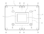
- the solid-state imaging device 1 includes a pixel array unit 4 that forms a pixel region (imaging region) in which a plurality of pixels 3 are two-dimensionally arranged in a matrix on a semiconductor substrate 2, and a peripheral circuit provided around the pixel array unit 4 And a peripheral circuit section 5 forming a region (logic region).
- the pixel 3 is formed on the semiconductor substrate 2. Note that the form of the arrangement of the plurality of pixels 3 is not particularly limited.
- the pixel array unit 4 includes an effective pixel area 6 that generates, amplifies, and reads signal charges by photoelectric conversion in each pixel 3, and an area formed around the effective pixel area 6. And an OPB (Optical Black) region 7.
- an effective pixel area 6 that generates, amplifies, and reads signal charges by photoelectric conversion in each pixel 3, and an area formed around the effective pixel area 6.
- a rectangular effective pixel area 6 is provided at the center thereof, and an OPB area 7 is provided so as to surround four sides of the effective pixel area 6.
- the OPB area 7 is an area for outputting a signal (optical black) serving as a black level reference to the effective pixel area 6 for outputting the signal charge as an effective pixel signal.
- the pixels 3 formed in the OPB region 7 are shielded from light by a light shielding film (FIG. 4, OPB formation light shielding film 40B), and a signal from the light-shielded pixel 3 is used as a black level reference.
- the pixel 3 includes a photodiode as a photoelectric conversion unit having a photoelectric conversion function and a plurality of pixel transistors.
- the photodiode has a light receiving surface, and generates a signal charge in an amount corresponding to the amount of light (intensity) of light incident on the light receiving surface.
- the plurality of pixel transistors include, for example, MOS transistors that respectively handle amplification, transfer, selection, and resetting of signal charges generated by photodiodes.
- the plurality of pixels 3 may have a shared pixel structure in which the photodiodes and transfer transistors constituting the plurality of unit pixels are configured by sharing other pixel transistors one by one.
- the shared pixel structure includes a plurality of photodiodes, a plurality of transfer transistors, one shared floating diffusion (floating diffusion region), and one shared other pixel transistor.
- the peripheral circuit unit 5 includes a vertical drive circuit 8, a column signal processing circuit 9, a horizontal drive circuit 10, an output circuit 11, and a control circuit 12.
- the vertical drive circuit 8 is configured by, for example, a shift register, selects a predetermined pixel drive wiring 13, supplies a drive pulse for driving the pixel 3 to the selected pixel drive wiring 13, and drives the pixels 3 in units of rows. To do.
- the vertical drive circuit 8 selectively scans each pixel 3 of the pixel array unit 4 in the vertical direction sequentially in units of rows, and outputs a pixel signal based on a signal charge generated in the photodiode of each pixel 3 through the vertical signal line 14 to the column.
- the signal processing circuit 9 is supplied.
- the column signal processing circuit 9 is a signal processing circuit that processes an output signal from each pixel 3. For example, it is provided for each column of the pixels 3, and a signal output from the pixels 3 for one row is processed for each column. Examples of signal processing performed by the column signal processing circuit 9 include CDS (Correlated Double Sampling), signal amplification, and AD (Analog / Digital) conversion for reducing fixed pattern noise unique to the pixel 3. Etc.
- CDS Correlated Double Sampling
- AD Analog / Digital
- the horizontal drive circuit 10 is configured by, for example, a shift register, and sequentially outputs horizontal scanning pulses to sequentially select the column signal processing circuit 9 and to send a pixel signal from each of the column signal processing circuits 9 to the horizontal signal line 15. Output.
- the output circuit 11 performs predetermined signal processing on the signals sequentially supplied from the column signal processing circuits 9 through the horizontal signal lines 15 and outputs the signals. Examples of signal processing performed by the output circuit 11 include buffering, black level adjustment, column variation correction, various digital signal processing, and the like. *
- the control circuit 12 receives data for commanding an operation mode, an input clock, etc., and outputs data such as internal information of the solid-state imaging device 1.
- the control circuit 12 generates a clock signal and a control signal that serve as a reference for the operation of the vertical drive circuit 8, the column signal processing circuit 9, and the horizontal drive circuit 10 based on the vertical synchronization signal, the horizontal synchronization signal, and the master clock. The generated signal is input to these circuits.
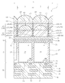
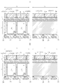
- FIGS. 3, 4, and 5 are cross-sectional views showing the layer structure of the effective pixel region 6
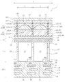
- FIG. 4 is a cross-sectional view showing the layer structure of the OPB region 7
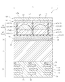
- FIG. 5 is a cross-sectional view showing a part of the layer structure of the peripheral circuit portion 5. It is.
- the photodiodes 21 included in the pixels 3 are formed mostly in the thickness direction of the semiconductor substrate 2.
- the photodiode 21 has an n-type semiconductor region 23 as a first conductivity type, and a p-type semiconductor region 24 as a second conductivity type formed so as to face both the front and back surfaces of the semiconductor substrate 2.
- a junction type photodiode is formed on a pixel basis.
- the p-type semiconductor region 24 also serves as a hole charge accumulation region for suppressing dark current.
- the plurality of pixel transistors 22 included in the pixel 3 are for reading signal charges accumulated in the photodiode 21 and have a source / drain region (not shown) and a gate electrode 25.
- the source / drain regions are formed as n-type regions in the p-type semiconductor well region 26 formed on the surface 2 a side, which is one plate surface side of the semiconductor substrate 2.
- the gate electrode 25 is formed on the surface 2a of the semiconductor substrate 2 between the source and drain regions via a gate insulating film.
- each pixel 3 including the photodiode 21 and the plurality of pixel transistors 22 is separated by the element isolation region 27 formed as a p-type semiconductor region.
- a laminated wiring layer 28 is formed on the surface 2 a side of the semiconductor substrate 2.
- the stacked wiring layer 28 has a plurality of wirings 30 stacked via an interlayer insulating film 29.
- the interlayer insulating film 29 is formed of, for example, a silicon oxide film formed of silicon dioxide (SiO 2 ).
- the plurality of wirings 30 are made of different metals, for example.
- the wiring layer provided on the surface 2a side of the semiconductor substrate 2 may be a wiring layer having a single layer structure.
- an insulating film 31 that optically functions as an antireflection film is formed on the back surface 2b, which is the other plate surface of the semiconductor substrate 2.
- the insulating film 31 has a stacked structure in which a plurality of films having different refractive indexes are stacked.
- the insulating film 31 has a two-layer structure including a silicon oxide film 32 and a hafnium oxide film 33.
- a planarizing film 34 having optical transparency is formed on the insulating film 31, a planarizing film 34 having optical transparency is formed.
- the planarization film 34 is formed of, for example, an organic material such as resin or an oxide film.
- a light shielding film 40 is formed on the planarizing film 34.
- the light shielding film 40 is formed as an inter-pixel light shielding film 40A at the pixel boundary portion on the planarizing film 34 (see FIG. 3).
- the inter-pixel light-shielding film 40A is a linear layer portion formed along the boundary between adjacent pixels 3, and is formed in a lattice shape in plan view.
- the inter-pixel light shielding film 40A suppresses optical color mixing or the like between pixels.
- the light shielding film 40 is formed as an OPB forming light shielding film 40B that entirely covers the planarizing film 34 (see FIG. 4).
- the OPB formation light shielding film 40B forms a region for detecting a black level that is a reference for dark output.
- the inter-pixel light-shielding film 40A and the OPB formation light-shielding film 40B are not limited to the same layer formed as the light-shielding film 40 at the same time, and may be individually formed as different layers.
- the light shielding film 40 is formed of a material that shields light.
- a material for forming the light-shielding film 40 a material suitable for microfabrication is preferable so that the light-shielding property is strong and can be processed with high accuracy by, for example, etching.
- the material for forming the light shielding film 40 is, for example, a metal such as tungsten (W), aluminum (Al), or copper (Cu).
- a light shielding wall layer 43 composed of the light shielding wall 41 and the planarizing film 42 is formed in a plurality of stages (in this embodiment, two stages).
- the light shielding wall 41 is configured to prevent the incidence of oblique light from adjacent pixels.
- the light shielding wall 41 is formed on the pixel boundary portion along the boundary between the adjacent pixels 3 on the light shielding film 40 and has a lattice shape in plan view.
- the light shielding wall 41 is formed of a metal material such as tungsten or aluminum in the same manner as the light shielding film 40.
- the planarizing film 42 is formed of an inorganic material such as SiO 2 .
- the lower light shielding wall layer 43L has a first light shielding wall portion 41L formed on the inter-pixel light shielding film 40A or the OPB formation light shielding film 40B.
- a first planarizing film 42L is formed between the first light shielding wall portions 41L.
- the upper light shielding wall layer 43H has a second light shielding wall 41H formed on the first light shielding wall 41L.
- a second planarizing film 42H is formed between the second light shielding wall portions 41H.
- An inner lens 45 that is an in-layer lens is formed on the upper light shielding wall layer 43H.
- the inner lens 45 is formed for each pixel 3 corresponding to the photodiode 21 that constitutes the pixel 3.
- the inner lens 45 is formed of an inorganic material such as SiN (silicon nitride), for example. There may be a pixel 3 that does not have the inner lens 45.
- the light shielding wall layer 43 has a two-stage structure, but the light shielding wall layer 43 may have a one-stage structure or a three-stage structure or more.
- the inner lens 45 is formed on the upper light shielding wall layer 43H.
- the light shielding wall layer 43 forming the inner lens 45 is not particularly limited, and the inner lens 45 has a plurality of light shielding layers.
- the wall layer 43 may be formed.
- a color filter layer 46 is formed on the upper light shielding wall layer 43H.
- the color filter layer 46 is divided into a plurality of color filters 47 formed corresponding to each pixel 3.
- the color filter 47 is, for example, a filter portion of any color of red (R), green (G), and blue (B), and transmits light of each color component.
- the color filter 47 is a so-called on-chip color filter, and is formed according to a predetermined arrangement such as a Bayer arrangement.
- the second light shielding wall portion 41H of the upper light shielding wall layer 43H may be formed so as to protrude into the color filter layer 46 in order to shield between the adjacent color filters 47.
- a lens layer 48 having a plurality of microlenses 49 is formed on the color filter layer 46.
- the micro lens 49 is a so-called on-chip lens, and is formed for each pixel 3 corresponding to the photodiode 21 constituting the pixel 3. That is, the microlens 49 is formed on each color filter 47.
- the micro lens 49 is formed of, for example, a resin organic material or an inorganic material such as SiN (silicon nitride).
- the lens layer 48 is a flat layer portion 48a formed of a material forming the microlens 49 (see FIG. 4). *
- the peripheral circuit unit 5 for example, at least a part of the peripheral portion of the pixel array unit 4, etc., with respect to the layer structure on the front surface 2 a side and the back surface 2 b side of the semiconductor substrate 2.
- a portion (hereinafter referred to as “array development unit”) having a layer structure in which the array is developed is provided.
- the lens layer 48 is a flat layer portion 48 a similar to the OPB region 7.
- the light shielding film 40 is formed as a solid light shielding film 40 ⁇ / b> C that covers the entire planarizing film 34, as in the OPB region 7.
- the solid light-shielding film 40C is not limited to the same layer formed simultaneously as the light-shielding film 40 in the relationship between the inter-pixel light-shielding film 40A and the OPB-forming light-shielding film 40B, and is separately formed as a different layer. It may be a thing.
- the solid-state imaging device 1 includes the laminated wiring layer 28 that is formed on the surface 2 a side of the semiconductor substrate 2 in the peripheral circuit unit 5 and includes the transistor 20 and the wiring 30.
- the color filter layer 46 and the microlens 49 are provided on the back surface 2b side opposite to the front surface 2a side on which the laminated wiring layer 28 is provided. And has a back-illuminated structure in which the back surface 2b side is the light incident side. According to the structure on the backside irradiation side, the laminated wiring layer 28 is provided on the side opposite to the light incident side (front surface 2a side) with respect to the semiconductor substrate 2, and therefore the layout of the wirings 30 and the like constituting the laminated wiring layer 28 is provided. High degree of freedom can be obtained.
- incident light is collected by the microlens 49 on the color filter 47, passes through the color filter layer 46, and is further collected by the inner lens 45 in the upper light shielding wall layer 43H.
- Light is received by the diode 21. Thereby, high condensing efficiency with respect to the photodiode 21 is obtained, and good sensitivity is obtained.
- an n-type semiconductor region 23 is formed for each pixel 3 in the p-type semiconductor region 24 of the semiconductor substrate 2, so that the photodiode 21 is in pixel units. Formed with.
- the laminated wiring layer 28 including the pixel transistor 22, the plurality of wirings 30, and the interlayer insulating film 29 is formed on the surface 2 a side of the semiconductor substrate 2.
- the peripheral circuit transistor 20 is formed in the laminated wiring layer 28. Further, a silicon oxide film 32, a hafnium oxide film 33, and a planarizing film 34 that form an insulating film 31 are formed on the back surface 2b side of the semiconductor substrate 2.
- a light shielding film 40 is formed on the planarizing film 34. That is, in the effective pixel region 6, the inter-pixel light shielding film 40 ⁇ / b> A is formed at the pixel boundary portion on the planarizing film 34, and the solid light shielding film 40 ⁇ / b> C is formed so as to cover the planarizing film 34 in the peripheral circuit unit 5. It is formed. In the OPB region 7, as in the peripheral circuit portion 5, an OPB formation light-shielding film 40B is formed so as to cover the planarization film 34 (see FIG. 4).
- the inter-pixel light shielding film 40A, the OPB forming light shielding film 40B, and the solid light shielding film 40C are simultaneously formed of the same material as the light shielding film 40. *
- the light shielding film 40 is formed by forming a film on the planarizing film 34 with a predetermined metal material such as tungsten, and a mask process for selectively forming a resist mask on the metal layer formed by the film forming process. And a removing step of selectively removing the metal layer through a resist mask.
- a predetermined metal material such as tungsten
- a film forming process for example, a sputtering method, a CVD (Chemical Vapor Deposition) method, a plating process, or the like is used, and a film (metal layer) made of a predetermined metal material is formed on the planarizing film 34.
- a resist mask is formed on the metal layer by patterning using a photolithography technique.
- the resist mask is formed along the portion corresponding to the inter-pixel light-shielding film 40A in the effective pixel region 6, that is, along the boundary portion between the plurality of pixels 3.
- the OPB is formed in the OPB region 7 and the peripheral circuit unit 5.
- the planarizing film 34 is formed so as to cover the portions corresponding to the light shielding film 40B and the solid light shielding film 40C.
- the resist mask is removed by etching such as wet etching or dry etching, and the metal layer is selectively removed by etching.
- a first planarizing film 42L is formed as shown in FIG. 7A.
- a first planarization film 42L is formed on the planarization film 34 and the inter-pixel light-shielding film 40A.
- the first planarization film 40C is formed on the solid light-shielding film 40C.
- a chemical film 42L is formed.
- the first planarization film 42L is formed on the OPB formation light shielding film 40B.
- an inorganic material such as a silicon oxide film (SiO 2 ) is formed, and then planarized by CMP (Chemical Mechanical Polishing) or the like, thereby forming the planarization layer 42X that becomes the first planarization film 42L. Is formed.
- CMP Chemical Mechanical Polishing
- the planarization layer 42X a portion for forming the first light shielding wall portion 41L is opened, and an opening portion 42a is formed.
- the opening 42 a is formed along a boundary portion between the plurality of pixels 3. Therefore, in the effective pixel region 6, the opening 42a is formed on the inter-pixel light shielding film 40A.
- the opening 42a is formed by etching the planarizing layer 42X.
- the entire surface is flattened by CMP or the like, whereby the first light shielding wall 41L is formed.
- An adhesion layer made of, for example, titanium nitride (TiN) is formed on the inner peripheral surface of the opening 42a.
- the lower light shielding wall layer 43L is formed.
- the first light-shielding wall 41L is formed first, depending on the type of the metal material forming the first light-shielding wall 41L, and then the first planarizing film 42L is formed. Can also be formed.
- the first light shielding wall 41L is formed by patterning the metal layer formed of the metal material to be the first light shielding wall 41L by photolithography. Thereafter, an inorganic material to be the first planarizing film 42L is embedded between the first light shielding walls 41L, and the entire surface is planarized by CMP or the like, thereby forming the lower light shielding wall layer 43L.
- the inner lens 45 is formed on the lower light shielding wall layer 43L. Specifically, first, a layer made of an inorganic material such as SiN (silicon nitride) that is a material of the inner lens 45 is formed on the lower light shielding wall layer 43L. Thereafter, a photoresist made of a predetermined photosensitive material is formed into a lens shape on the formed layer by a predetermined heat treatment or the like. Then, by using the lens-shaped photoresist as a mask, the inner lens 45 is formed by pattern transfer of the lens shape to a layer made of the material of the inner lens 45 by etching such as dry etching.
- 8A, 8B, 9A, and 9B show cross-sectional views of the effective pixel region 6, but the same process is performed in the OPB region 7 and the array development portion of the peripheral circuit portion 5.
- a second planarizing film 42H is formed on the inner lens 45 by the same method as the first planarizing film 42L. That is, first, on the inner lens 45, film formation and planarization with an inorganic material such as SiO 2 are performed, and a planarization layer 42Y to be the second planarization film 42H is formed. Next, an opening 42b for forming the second light shielding wall 41H is formed in the planarizing layer 42Y by etching. Here, the opening 42b is formed along a boundary portion between the plurality of pixels 3 corresponding to the planar shape of the first light shielding wall 41L. The opening 42b penetrates the material for forming the planarizing layer 42Y and the inner lens 45 below the planarizing layer 42Y.
- the second light shielding wall 41H is formed by embedding a predetermined metal material such as tungsten in the opening 42b and flattening. As described above, the upper light shielding wall layer 43H is formed. In addition, when forming the light shielding wall layer 43 in three steps or more, the process similar to the formation process of the light shielding wall layer 43 as mentioned above is repeated according to the number of steps.
- the color filter layer 46 is formed on the upper light shielding wall layer 43H.
- a color filter 47 of each color is formed by spin-coating a photosensitive resin containing a pigment such as a pigment or a dye, and a color filter layer 46 divided into a plurality of color filters 47 is formed. .
- a coating process, an exposure process, and a development process for applying a photosensitive resin are performed in a predetermined order. Is called. That is, for example, first, a coating process, an exposure process, and a development process for forming a green (G) color filter 47 are performed, and then a coating process for forming a blue (B) color filter 47. Then, an exposure process and a development process are performed, and thereafter, a coating process, an exposure process, and a development process for forming the red (R) color filter 47 are performed.
- the order of formation of the color filters 47 by color is not particularly limited.
- a photosensitive resin corresponding to the color of the color filter 47 to be formed is applied to form a filter film of the corresponding color.
- an exposure apparatus is used, and the filter film is exposed by light that passes through a photomask disposed above the filter film formed in the coating process, and a portion of the filter film that remains as the color filter 47 is exposed. Cured.
- a pattern corresponding to the color filter 47 to be formed is formed on the photomask.
- the portion that is shielded from light and not cured in the exposure step is removed by etching using a developer. Thereby, the color filter 47 of the corresponding color is formed at a position according to a predetermined arrangement such as a Bayer arrangement.
- the color filter 47 is embedded between the protruding portions of the second light shielding wall portion 41H.
- the presence / absence and color of the color filter 47 are not limited.
- a lens layer 48 is formed on the color filter layer 46 by a known method. Specifically, for example, a photoresist made of a photosensitive material is formed into a lens shape by a predetermined heat treatment on the material of the microlens 49 formed on the color filter layer 46, and the photoresist is etched by etching. The microlens 49 is formed by pattern transfer of the lens shape. As an example of a form of forming the lens layer 48, in the effective pixel region 6, a micro lens 49 is formed for each pixel 3, and in the OPB region 7 and the array development portion of the peripheral circuit portion 5, a flat layer portion 48 a is formed. It is formed.
- the solid-state imaging device 1 As described above, the solid-state imaging device 1 according to this embodiment is manufactured.
- the solid-state imaging device 1 is generally arranged and formed at regular intervals in a direction orthogonal to each other on a wafer of a disk-shaped semiconductor substrate 2, and is cut along a predetermined scribe region in a dicing process. Thus, it is obtained as an individual semiconductor chip.
- the solid-state imaging device 1 is formed on the semiconductor substrate 2 including the photodiode 21 formed for each pixel 3, and on one surface (front surface 2a) side of the semiconductor substrate 2, and the transistor (Pixel transistor 22, peripheral circuit transistor 20) and laminated wiring layer 28 as a wiring layer including wiring 30, light shielding film 40 provided on the other surface (back surface 2b) side of semiconductor substrate 2, and pixel 3
- a color filter layer 46 including the color filter 47 formed every time, and an intermediate layer formed between the light shielding film 40 and the color filter layer 46 are provided.
- the intermediate layer formed between the light shielding film 40 and the color filter layer 46 is at least one light shielding wall layer 43 among the light shielding wall layers 43 provided in a plurality of stages.
- the solid-state imaging device 1 includes a color filter layer 46 and a lens layer 48 as layers formed by performing divided exposure using an exposure region divided into a plurality of regions in a photolithography process in the manufacturing process. including. That is, in the exposure process in the process of forming the color filter layer 46 and the lens layer 48 as described above, an exposure apparatus in which the batch exposure area (exposure angle of view) is smaller than the chip size of the solid-state imaging device 1 is used. Thus, the exposure range corresponding to the entire chip size area is divided into a plurality of regions. Then, a photomask having a pattern corresponding to each divided area is used to perform exposure for each divided area, and by joining these areas, a pattern of the entire chip surface can be obtained.
- the exposure area by the exposure device is formed on the rectangular chip surface 50 corresponding to the outer shape of the solid-state imaging device 1.
- the left exposure area 51 is a first exposure area
- the right exposure area 52 is a second exposure area
- the central exposure area 53 is a third exposure area.
- the longitudinal direction (left-right direction in FIG. 10) of the chip surface 50 be the left-right direction.
- the central exposure region 53 is located in the central portion of the chip surface 50 with the longitudinal direction being the left-right direction, and includes the entire portion where the pixel array portion 4 is formed. As a result, the entire effective pixel region 6 is exposed at once.
- the area portion outside the pixel array section 4 in the central exposure area 53 is the peripheral circuit section 5 (see FIG. 2).
- areas obtained by dividing the chip surface 50 into approximately two equal parts to the left and right become a left exposure area 51 and a right exposure area 52, respectively.
- the longitudinal direction is the short direction of the chip surface 50 (the vertical direction in FIG. 10).
- a photomask having a pattern corresponding to each divided area is used as a photomask, and exposure is performed for each divided area, and these areas are joined together.
- a pattern of the entire chip surface 50 is obtained. Therefore, in the divided exposure according to the present embodiment, as a photomask, as shown in FIG. 10, the first mask 61 used for exposure of the left exposure region 51 and the second mask 62 used for exposure of the right exposure region 52 are used. , And three photomasks of the third mask 63 used in the exposure of the central exposure region 53 are used.
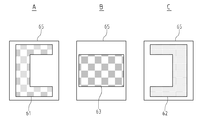
- FIG. 11 shows an image diagram of the layout of each mask at the exposure angle of view 65 which is a batch exposure region.
- FIG. 11A shows the layout of the first mask 61 at the exposure angle of view 65.
- FIG. 11B shows the layout of the third mask 63 at the exposure angle of view 65.
- FIG. 11C shows the layout of the second mask 62 at the exposure angle of view 65.
- the exposure angle of view 65 is smaller than the area of the chip surface 50, and the exposure using the masks 61, 62, 63 is performed on the exposure regions 51, 52, 53 described above.
- a case where the color filter layer 46 is formed will be described with respect to divided exposure.
- exposure using each mask is performed in a predetermined order for each color of the color filter 47.
- the exposure process for forming the green (G) color filter 47 first, the first exposure of the left exposure region 51 using the first mask 61 is performed, and then the second mask 62 is removed. The second exposure is performed on the used right exposure region 52, and then the third exposure is performed on the central exposure region 53 using the third mask 63.
- the irradiation light and the wafer are moved between the second exposure and the third exposure by the operation of the optical system provided in the exposure apparatus or the stage on which the wafer is placed.
- the relative position of 90 is relatively rotated.
- the orientation of the exposure angle of view 65 for the first to third exposures is the same, so in the first to third exposures, the irradiation light and the wafer The positional relationship is constant.
- the order of the first exposure, the second exposure, and the third exposure is not particularly limited. The exposure process using these three photomasks is performed for each color of the color filter 47 having a different formation pattern. Therefore, three photomasks are prepared for each color of the color filter 47.
- the shape of the effective exposure area by each photomask becomes a shape as shown in FIGS. That is, the third mask 63 used for the exposure of the central exposure region 53 has a shape of an effective exposure region in the entire rectangular region shape.
- the first mask 61 used for the exposure of the left exposure area 51 where the left half of the center exposure area 53 overlaps has a substantially “U” shape with the right side as the opening side, excluding the overlapping part of the center exposure area 53.
- a substantially “U” -shaped region shape is an effective exposure region shape.
- the second mask 62 used for the exposure of the right exposure region 52 where the right half of the central exposure region 53 overlaps is substantially “U” -shaped with the left side being the opening side excluding the overlapping portion of the central exposure region 53 or
- a substantially “U” -shaped region shape is an effective exposure region shape.
- a first configuration example of the alignment mark will be described.
- a mark for alignment is provided at a part corresponding to the predetermined part.
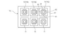
- mark regions 68, 69 which are alignment mark formation regions, are formed at portions corresponding to the four corners of each of the rectangular exposure regions 51, 52, 53. 70 is provided (see FIGS. 2 and 10).
- a mark portion serving as a reference for measuring the positional relationship is formed in each of the mark areas 68, 69, and 70.
- the mark area 70 formed in a portion included in the central exposure area 53 will be described.
- the mark region 70 is formed at portions corresponding to the four corners of the central exposure region 53, and the mark region 70 is formed in a region near the outer corners of the pixel array unit 4 in the peripheral circuit unit 5. 2).
- the mark area 70 is, for example, a rectangular area, and has a plurality of unit mark areas 71.
- the mark area 70 includes six unit mark areas 71 arranged in 2 rows and 3 columns.
- the unit mark region 71 has a substantially square shape.
- the size of one unit mark region 71 is, for example, a size including several tens of pixels 3.
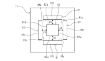
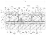
- each unit mark region 71 is a main scale 81 as a first mark portion provided in the upper light shielding wall layer 43H as the above-described intermediate layer as an alignment mark.
- a vernier 82 as a second mark portion that is formed on the color filter layer 46 and whose positional relationship with the main measure 81 is measured. Since the color filter layer 46 is a layer formed above the light shielding wall layer 43, the vernier 82 is formed above the main scale 81.
- FIG. 14 shows the layer structure of the solid-state imaging device 1, and the size relationship between the unit mark area 71 and the pixel 3, the ratio of the dimensions of each part, and the like do not necessarily match those in reality.
- the vernier 82 is formed at the center and has a square outer shape in plan view. As shown in FIG. 14, the vernier 82 is formed simultaneously with the color filter 47 as a part of the color filter layer 46 using the same material as the color filter 47 of any color in the color filter layer 46.
- the main scale 81 has four positions so as to surround the four sides of the vernier 82 at positions outside the side surface 82 a that forms each side of the square vernier 82. Is provided.
- the main scale 81 has an elongated rectangular outer shape that is formed in parallel with each side surface 82 a of the vernier 82 as a planar view shape, that is, along each side surface 82 a of the vernier 82.
- the four main scales 81 are arranged along the side surfaces 82a of the vernier 82 in the longitudinal direction, and each side except for the four corners of the square shape surrounding the outer periphery of the vernier 82 is formed. It is arranged and formed so as to surround the outer periphery of the vernier 82 in a substantially square shape.
- Each main measure 81 has a shape in plan view, and a side surface forming a side on the side of the vernier 82 is a side wall surface 81 a that faces the side surface 82 a of the vernier 82 in parallel.
- the main scale 81 is formed as a portion of the same layer as the light shielding wall 41 constituting the light shielding wall layer 43. That is, in the solid-state imaging device 1 according to the present embodiment, the light shielding wall layer 43 as an intermediate layer has a light shielding wall 41 formed between the pixels 3, and the main scale 81 is shielded by the material forming the light shielding wall 41. It is formed as a part of the same layer as at least a part of the wall 41.
- the light shielding wall 41 is formed in two layers by a lower light shielding wall layer 43L and an upper light shielding wall layer 43H.
- the main scale 81 is formed as a layer portion of the first light shielding wall portion 41 ⁇ / b> L of the two stages of the light shielding walls 41.
- the main scale 81 is a metal material such as tungsten that forms the first light shielding wall portion 41L in the first planarization film 42L in the lower light shielding wall layer 43L, as in the first light shielding wall portion 41L. Thus, it is formed as a wall-shaped part.
- the main scale 81 is a wall-shaped part formed in a state of being erected vertically with respect to the upper surface 40d of the solid light-shielding film 40C, and like the first light-shielding wall part 41L, the lower light-shielding wall layer It has a height corresponding to a film thickness of 43L.
- the side wall surface 81a of the main scale 81 and the side wall surface 81b on the opposite side thereof are vertical wall surfaces with respect to the upper surface 40d of the solid light shielding film 40C.
- the main scale 81 is formed immediately above the solid light shielding film 40C.
- the main scale 81 is formed simultaneously with the first light shielding wall 41L as the same layer portion as the first light shielding wall 41L. That is, as shown in FIG. 7A, in the planarization layer 42X that becomes the first planarization film 42L, the main scale 81 is formed simultaneously with the formation of the opening 42a for forming the first light shielding wall 41L. An opening 42c (see FIG. 14) is formed in the portion. Then, as shown in FIG. 7B, a predetermined metal material such as tungsten for forming the first light shielding wall 41L is embedded in the opening 42c, and then the entire surface is planarized by CMP or the like, whereby the first The main scale 81 is formed simultaneously with the light shielding wall 41L.
- An adhesion layer made of, for example, titanium nitride (TiN) is formed on the inner peripheral surface of the opening 42c, similarly to the first light shielding wall 41L. Further, even when the first light shielding wall 41L is formed before the first planarization film 42L depending on the type of the metal material forming the first light shielding wall 41L, the first light shielding wall 41L At the same time, the main scale 81 is formed.
- the main scale 81 is not limited to the same layer formed at the same time as the first light shielding wall 41L, and may be formed separately from the first light shielding wall 41L.
- the overlay accuracy such as the joining state between the plurality of exposure areas as described above and the formation position of the color filter 47 forming the color filter layer 46 is measured.
- the measured content is fed back to the formation of the color filter 47 of another color, for example.
- the positional relationship between the main scale 81 and the vernier 82 is not limited to the above example, and for example, a coordinate difference between the planar center positions of the main scale 81 and the vernier 82 may be measured.
- Each unit mark area 71 included in the mark area 70 is formed with a vernier 82 at the same time when the color filter 47 of any color among the color filters 47 of the plurality of colors forming the color filter layer 46 is formed.
- the vernier 82 is formed as a part of the color filter layer 46 by the same material as the color filter 47 of the color in the unit mark region 71 used when forming the color filter 47 of any color.
- one unit mark area 71G among the plurality of unit mark areas 71 included in the mark area 70 is used.
- the upper right unit mark area 71 in FIG. 12 is defined as a unit mark area 71G for green (G).
- the unit mark area 71 adjacent to the left of the unit mark area 71G for green (G) is used as the unit mark area 71B for blue (B) used in the process of forming the color filter 47 for blue (B).
- the unit mark region 71 on the left side is a unit mark region 71R for red (R) used in the step of forming the red (R) color filter 47.
- R red
- a case where the pixel array is a Bayer array and the color filter 47 is formed in the order of green (G), blue (B), and red (R) will be described as an example.
- the vernier 82 is formed in the unit mark region 71G for forming the green (G) color filter 47. That is, as shown in FIG. 15A, the unit mark region 71G includes the third exposure for the central exposure region 53 using the third mask 63 in the step of forming the green (G) color filter 47G.
- a vernier 82G made of the same material as that of the green (G) color filter 47G is formed as the vernier 82 simultaneously with the green (G) color filter 47G.
- the vernier 82 is formed in the unit mark region 71B for forming the blue (B) color filter 47. That is, as shown in FIG. 15B, the unit mark region 71B includes the third exposure for the central exposure region 53 using the third mask 63 in the step of forming the blue (B) color filter 47B.
- a vernier 82B made of the same material as that of the blue (B) color filter 47B is formed as the vernier 82 simultaneously with the blue (B) color filter 47B.
- the red (R) color filter 47R in the unit mark region 71R for forming the red (R) color filter 47R, the red (R) color filter 47R and the red scale (82) A vernier 82R made of the same material as the color filter 47R of R) is formed.
- the remaining unit mark area 71 is provided as a spare, for example.
- the mark area 70 Since each unit mark area 71 is used as described above, the mark area 70 has at least the number of unit mark areas 71 of the color type of the color filter 47.
- the shape, the number, and the like of the main scale 81 and the sub-scale 82 are not limited to the present embodiment.
- As the main scale 81 and the sub-scale 82 an appropriate configuration can be adopted as long as the positional relationship can be measured in a plan view.
- alignment marks can be formed while avoiding the risk of light leakage, and a reduction in the degree of freedom in circuit design can be suppressed.
- the main scale 81 is formed as the same layer portion as the first light shielding wall 41L above the solid light shielding film 40C, and the sub-scale 82 is formed in the color filter layer 46 thereabove. Yes.
- the light shielding function by the solid light shielding film 40C is secured, a part of incident light with respect to the solid-state imaging device 1 is prevented from leaking light incident on the pixels 3 in the effective pixel region 6 as oblique light or the like. can do.
- light leakage to the pixel 3 in the effective pixel region 6 is caused by driving a circuit such as the pixel transistor 22 provided on the opposite side of the light incident side of the semiconductor substrate 2 to read out the charge accumulated in the photodiode 21. Also has an adverse effect. Therefore, since the light leakage can be prevented as described above, it is not necessary to avoid the influence of the light leakage on the arrangement of the pixel transistor 22 and the like, so that the degree of freedom in circuit design for the pixel transistor 22 and the like can be improved.
- the main scale 81 is formed as a part of the same layer as a part of the upper and lower light shielding walls 41 constituting the light shielding wall layer 43 having a two-stage structure. According to such a configuration, the main scale 81 can be formed at the same time in the process of forming the light shielding wall 41. Therefore, the main scale 81 can be easily formed without increasing the number of processes or preparing a separate material. It becomes possible to do.
- the main scale 81 is formed as a layer portion of the first light shielding wall portion 41L constituting the lower light shielding wall layer 43L in the two-stage light shielding wall layer 43. According to such a configuration, the main scale 81 can be formed simultaneously with the first light shielding wall 41L by the same method as the first light shielding wall 41L, and the main scale 81 is easily and reliably formed. It becomes possible.
- Second Configuration Example of Positioning Mark> A second configuration example of the alignment mark will be described with reference to FIG. In each configuration example described below, common or corresponding configurations are denoted by the same reference numerals, and description thereof is omitted as appropriate.
- the main scale 81 is formed as a layer portion of the second light shielding wall portion 41H of the two stages of light shielding walls 41. Therefore, the main scale 81 is made of a metal material that forms the second light shielding wall 41H in the second planarization film 42H in the upper light shielding wall layer 43H, as in the second light shielding wall 41H. It is formed as a shaped part.
- the main scale 81 is a wall-shaped part formed in a manner standing upright with respect to the upper surface 42d of the first planarizing film 42L, and is similar to the second light shielding wall 41H. It has a height corresponding to the film thickness of the light shielding wall layer 43H.
- the side wall surface 81a of the main scale 81 and the opposite side wall surface 81b are wall surfaces perpendicular to the upper surface 42d of the first planarizing film 42L. It becomes.
- the main scale 81 is formed between the solid light shielding film 40C and the vernier 82 in the vertical direction (stacking direction of the layer structure) in a portion above the solid light shielding film 40C. .
- the shape and arrangement of the main scale 81 in plan view are the same as those in the first configuration example.
- the main scale 81 is formed simultaneously with the second light shielding wall portion 41H as the same layer portion as the second light shielding wall portion 41H. That is, as shown in FIG. 8B, the main scale 81 is formed simultaneously with the formation of the opening 42b for forming the second light shielding wall 41H in the planarization layer 42Y to be the second planarization film 42H. An opening 42e (see FIG. 16) is formed in the portion. Then, after embedding a predetermined metal material for forming the second light shielding wall 41H in the opening 42e, the entire surface is flattened by CMP or the like, so that the main scale 81 is simultaneously formed with the second light shielding wall 41H. Is formed.
- the main scale 81 is not limited to the same layer formed simultaneously with the second light shielding wall 41H, and may be formed separately from the second light shielding wall 41H.
- the main scale 81 is formed as a layer portion of the second light shielding wall portion 41H constituting the upper light shielding wall layer 43H in the two-stage light shielding wall layer 43.
- the main scale 81 can be formed simultaneously with the second light-shielding wall portion 41H by the same method as the second light-shielding wall portion 41H, and the main scale 81 can be formed easily and reliably.
- the main scale 81 approaches the vernier 82 in the vertical direction in comparison with the first configuration example, and accordingly, the measurement of the positional relationship between the main scale 81 and the vernier 82 is highly accurate. Measurement with this is possible.
- the main scale 81 is formed as a layer portion of the first light shielding wall portion 41L and the second light shielding wall portion 41H of the two-stage light shielding walls 41. That is, in the present configuration example, the main scale 81 includes a lower main scale portion 81x that is a layer portion of the first light shielding wall portion 41L and an upper main scale portion 81y that is a layer portion of the second light shielding wall portion 41H. It is formed as an integral wall-like part with two upper and lower stages.
- the lower main scale portion 81x is formed simultaneously with the first light shielding wall portion 41L as the same layer portion as the first light shielding wall portion 41L.
- the upper main scale portion 81y is formed simultaneously with the second light shielding wall portion 41H as the same layer portion as the second light shielding wall portion 41H.
- the upper main scale portion 81y constituting the main scale 81
- the upper main scale portion 81y is formed on the lower main scale portion 81x, so that the first main light shielding wall portion 41L is formed on the first light shielding wall portion 41L.
- the upper main scale portion 81y can be formed under the same formation conditions as the second light shielding wall portion 41H. For this reason, the main scale 81 can be formed more easily.
- the main scale 81 is formed between the solid light-shielding film 40C and the vernier 82 by the forming material of the inner lens 45. That is, in the solid-state imaging device 1 according to the present embodiment, the light shielding wall layer 43 as an intermediate layer has an inner lens 45 formed in units of three pixels, and the main scale 81 is made of an inner lens 45 by a material forming the inner lens 45. It is formed as a part of the same layer as the lens 45.
- the main scale 81 is SiN (which forms the inner lens 45 in the second planarizing film 42H in the upper light shielding wall layer 43H where the inner lens 45 is formed. It is formed as a wall-shaped portion by an inorganic material such as silicon nitride.
- the main scale 81 is a wall-shaped portion formed in a manner standing vertically with respect to the upper surface 42d of the first planarizing film 42L, and has a height corresponding to the film thickness of the inner lens 45.
- the side wall surface 81a of the main scale 81 and the opposite side wall surface 81b are wall surfaces perpendicular to the upper surface 42d of the first planarizing film 42L. It becomes.
- the main scale 81 is formed between the solid light shielding film 40C and the vernier 82 in the vertical direction at a portion above the solid light shielding film 40C.
- the shape and arrangement of the main scale 81 in plan view are the same as those in the first configuration example.
- the main scale 81 is formed at the same time as the inner lens 45 as the same layer portion as the inner lens 45. That is, a photoresist is formed on the lower light-shielding wall layer 43 ⁇ / b> L at a portion corresponding to the main scale 81 with respect to the layer formed from the material for forming the inner lens 45. Then, the main scale 81 made of the material for forming the inner lens 45 is formed simultaneously with the inner lens 45 by the etching process for forming the inner lens 45.
- the main scale 81 is not limited to the same layer formed simultaneously with the inner lens 45, and may be formed separately from the inner lens 45.
- the main scale 81 is formed as a layer portion of the inner lens 45, and therefore, the main scale 81 can be formed simultaneously with the inner lens 45 by the same method as the inner lens 45. Thus, the main scale 81 can be easily and reliably formed.
- the main scale 81 approaches the vernier 82 in the vertical direction in comparison with the first configuration example, and accordingly, the measurement of the positional relationship between the main scale 81 and the vernier 82 is highly accurate. Measurement with this is possible.
- a process of forming the semiconductor substrate 2 including the photodiode 21 formed for each pixel 3 is performed.
- a step of forming a light shielding film 40 as an upper layer of the semiconductor substrate 2 is performed.
- the inter-pixel light-shielding film 40A, the OPB formation light-shielding film 40B, and the solid light-shielding film 40C are simultaneously formed as the light-shielding film 40.
- the step of forming the intermediate layer includes the step of forming the main scale 81.
- the main scale 81 is formed as a portion of the same layer as the first light shielding wall portion 41L in the step of forming the lower light shielding wall layer 43L.
- the main scale 81 is formed as a portion of the same layer as the second light shielding wall portion 41H in the step of forming the upper light shielding wall layer 43H.
- the lower main scale portion 81x, the second light shielding wall portion 41L, and the second layer in the first configuration example, in the step of forming the intermediate layer, the main scale 81 is formed as a portion of the same layer as the first light shielding wall portion 41L in the step of forming the lower light shielding wall layer 43L.
- the upper main scale part 81y of the same layer as the light shielding wall part 41H is formed, and the main scale 81 is formed by these main scale parts.
- the main scale 81 is formed as a portion in the same layer as the inner lens 45 constituting the upper light shielding wall layer 43H.
- a step of forming a color filter layer 46 including the color filter 47 formed for each pixel 3 on the intermediate layer is performed.
- the step of forming the color filter layer 46 includes the step of forming the vernier 82.
- the vernier 82 is formed as a part of the color filter layer 46 with the same material as the color filter 47 of that color.
- the overlay accuracy of the color filter layer 46 is measured by measuring the positional relationship between the main scale 81 and the vernier 82.
- the positional relationship between the main scale 81 and the sub-scale 82 is a dimension d1 to between the side wall surface 81a of each main scale 81 and each side surface 82a of the sub-scale 82. d4 is measured.
- the alignment mark can be formed while avoiding the risk of light leakage, and the reduction in the degree of freedom in circuit design is suppressed. Can do.
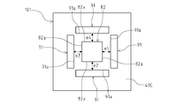
- each unit mark region 101 includes an opening-shaped main scale 91 formed on a solid light-shielding film 40C, which is a light-shielding film, and a color filter as alignment marks.
- the main scale 91 has four positions so as to surround the four sides of the vernier 82 at positions outside the side surface 82a forming each side of the square vernier 82. Is formed.
- the main scale 91 has an elongated rectangular opening shape that is formed along the side surfaces 82a of the vernier 82, that is, parallel to the side surfaces 82a of the vernier 82 as a plan view.
- the four main scales 91 have their longitudinal directions along the side surfaces 82a of the vernier 82, and each side excluding the four corners of the square shape surrounding the outer periphery of the vernier 82, It is arranged and formed so as to surround the outer periphery of the vernier 82 in a substantially square shape.
- Each main measure 91 has a shape in plan view, and a surface forming a side on the side of the vernier 82 is an inner side surface 91 a parallel to the side surface 82 a of the vernier 82.
- the main scale 91 is formed as an opening penetrating in the vertical direction in the solid light shielding film 40C in which the light shielding film 40 is formed in a solid shape.
- the inner side surface 91 a and the other inner side surface of the main scale 91 are surfaces that are perpendicular to the upper surface 34 c of the planarizing film 34.
- the main scale 91 is formed simultaneously with the light shielding film 40 as a part of the light shielding film 40. That is, as shown in FIG. 6B, in the mask process when forming the inter-pixel light-shielding film 40A, the OPB-forming light-shielding film 40B, and the solid light-shielding film 40C, the formation site of the main scale 91 is the formation of the resist mask in the solid light-shielding film 40C. In the subsequent removal process, the metal layer portion of the solid light shielding film 40C where the main scale 91 is formed is removed, and an opening as the main scale 91 is formed. The opening as the main scale 91 is filled with the first planarizing film 42L of the lower light shielding wall layer 43L formed on the light shielding film 40.
- the unit mark region 101 having the main measure 91 and the sub measure 82 as shown in FIG. 20, for example, as shown in FIG.
- the dimensions e1 to e4 between the side surfaces 82a of the vernier 82 are measured. Based on these measurement values, the state of joining between the plurality of exposure regions as described above, the formation position of the color filter 47 forming the color filter layer 46, and the like are grasped.
- the light shielding film 40 on which the main scale 91 is formed is formed as an upper layer with respect to the semiconductor substrate 2 on which the photodiode 21 is formed for each pixel 3.
- Each mark region 100 is located in the vicinity of the effective pixel region 6 in the peripheral circuit unit 5. For these reasons, there is a concern about the risk of light leakage in which a part of incident light with respect to the solid-state imaging device 1 enters the pixel 3 in the effective pixel region 6 as an oblique light or the like from the opening as the main scale 91.
- the region shape (plan view shape) of the mark region 100 is devised.
- the main scale 91 is formed in the mark region 100 having a predetermined region shape in the plate surface direction (horizontal direction) of the semiconductor substrate 2.
- the mark area 100 includes a plurality of unit mark areas 101 (five in this configuration example), and a main scale 91 and a sub scale 82 are formed in each unit mark area 101.
- the unit mark region 101 has an approximately square shape, and the size of one unit mark region 101 is, for example, a size including several tens of pixels 3.
- the mark area 100 is provided in an area around the effective pixel area 6.
- the mark area 100 is provided to the effective pixel area 6 via the OPB area 7 in an array development portion that is a portion near the pixel array section 4 in the peripheral circuit section 5. That is, in the peripheral circuit portion 5, the mark region 100 is formed in a portion near the outside of the four corners of the pixel array portion 4.
- the formation region of the mark region 100 is a region corresponding to the four corners of the central exposure region 53.
- region 100 has the notch part 102 which makes the effective pixel area 6 side the concave side as the area
- the mark region 100 includes two linear region portions 100a and 100b in which a plurality of unit mark regions 101 are arranged in a line, and these region portions 100a. , 100b have a substantially “L” -shaped region shape. That is, the two linear region portions 100a and 100b have substantially the same length and are arranged so as to be perpendicular to each other.
- the unit mark area 101 at the corner of the mark area 100 is the unit mark area 101A common to both the area portions 100a and 100b, the longitudinal direction of each of the area portions 100a and 100b.
- the three unit mark areas 101 are arranged in a line, and a total of five unit mark areas 101 are provided in the mark area 100.
- the inner portion of the substantially “L” -shaped region shape formed by the two region portions 100a and 100b is the notch portion 102.
- the region shape of the mark region 100 includes a long side 103 s outside the two region portions 100 a and 100 b, a short side 103 t on the end side of each region portion 100 a and 100 b, and An angle formed by two imaginary lines 103u with respect to a square-shaped outer shape formed by two short sides 103t and an imaginary line (two-dot chain line) 103u forming the diagonal side of the corners of two long sides 100s. It has a shape in which the side is cut out in a square shape. That is, the notch 102 is a recess formed by the long side 103v inside the two region portions 100a and 100b that are perpendicular to each other.
- each mark region 100 provided near the outside of the four corners of the pixel array portion 4 is formed so that the notch portion 102 side faces the effective pixel region 6 side (pixel array portion 4 side).
- each mark area 100 has a notch 102 on the effective pixel area 6 side as its area shape.
- the mark region 100 has a corner portion formed by two region portions 100a and 100b, with the longitudinal direction of each region portion 100a and 100b being parallel to each side of the rectangular pixel array portion 4. Are provided along the corners of the pixel array section 4. As shown in FIG. 21, the four mark regions 100 are arranged and formed so as to be symmetric with respect to the longitudinal direction (left-right direction in FIG. 21) and short-side direction (up-down direction in FIG. 21) of the pixel array unit 4 in plan view. ing.
- each mark area 100 has the cutout portion 102 in a plan view shape facing the effective pixel area 6 side.
- the mark region 100 shown in FIG. 22 is a mark region 100A located in the upper right of the four mark regions 100 in FIG.
- the opening portion as the main scale 91 of each unit mark region 101 is equivalent to the amount of the notch 102 formed.
- the shape of the cutout portion 102 and the shape of the entire mark region 100 including the cutout portion 102 are not limited to the above-described example.
- the opening portion of the main scale 91 is moved away from the effective pixel area 6 by having a concave cutout portion and setting the concave side of the cutout section to the effective pixel area 6 side. Any shape is acceptable.
- the main scale 91 is formed in the solid light-shielding film 40C as a slit-shaped opening.
- the region shape (planar shape) of the mark region 120 is devised from a viewpoint different from the fifth configuration example.
- the light shielding film 40 on which the main scale 91 is formed is formed as an upper layer with respect to the semiconductor substrate 2 on which the photodiode 21 is formed for each pixel 3. Further, a circuit such as a transistor 20 for a peripheral circuit is provided on the side opposite to the light incident side (surface 2a side) of the semiconductor substrate 2. For these reasons, for example, when the main scale 91 exists directly above the transistor 20 for the peripheral circuit, the light leaking from the opening as the main scale 91 out of the incident light on the solid-state imaging device 1 is the characteristic of the transistor 20. There is a concern that it will fluctuate. Therefore, in the present configuration example, the region shape of the mark region 120 is devised.
- the mark area 120 has a notch 122 for avoiding area overlap with the transistor 20 as the area shape.
- the present configuration example as shown in FIG. 23, three unit mark regions 101 arranged in the horizontal direction in the upper row and two unit marks arranged in the horizontal direction in the lower row. A total of five unit mark areas 101 with the area 101 are provided in the mark area 120.
- the lower two unit mark areas 121 have the same horizontal position as the two right unit mark areas 101 in the upper row.
- the area shape of the mark area 120 is an area shape in the case of having six unit mark areas 101 arranged in 2 rows and 3 columns (for example, the mark area 70 shown in FIG. 12).
- the shape of the rectangular shape that is formed by imaginary lines (two-dot chain lines) 120a that are diagonal to the upper right corner of the rectangular outer shape assumed as a reference) is cut into a rectangular shape.
- the notch 122 is a recess formed by sides 120 b that are perpendicular to each other on the lower left side of the mark region 120.
- the mark region 120 is provided so as not to overlap with the transistor 20 located therebelow by the notch 122, that is, not to overlap in the plan view.
- the mark region 120 has a notch portion 122 on the transistor 20 side as its region shape, and the notch portion due to the notch portion 122 is directly above the transistor 20 (20A) in plan view. It is formed so that it may be located in.
- the formation region of the transistor 20 (20A) is located in a rectangular region formed by the two sides 120b forming the notch 122 and the virtual line 120a. Further, other transistor 20 formation regions are provided at a plurality of positions in positions not overlapping the mark region 120 in plan view.
- the sixth configuration example as described above it is possible to easily avoid the opening portion as the main scale 91 being located immediately above the transistor 20 with respect to the layout of the mark region 120 by the notch portion 122. . Thereby, the influence on the characteristics of the transistor 20 due to light leaked from the opening as the main scale 91 can be minimized. As a result, alignment marks can be formed while avoiding the risk of light leakage, and the degree of freedom in circuit design of the transistor 20 can be improved. Then, by making the formation part of the notch 122 correspond to the formation part of the transistor 20, for example, the mark area 120 is arranged in the vicinity of the mark area 120 while avoiding the transistor 20 in comparison with the case where the mark area 120 is rectangular. Therefore, the space of the peripheral circuit unit 5 can be used effectively.
- the shape of the notch portion 122 and the shape of the entire mark region 120 including the notch portion 122 are not limited to the above-described example.
- As the shape of the mark region 120 a shape having a concave cut-out, which is located above or near the formation site of the transistor 20, avoiding regional overlap with the transistor 20. If it is.
- the main scale 91 is obtained. Can be moved away from the effective pixel area 6, and the influence of the light leaking from the main scale 91 on the imaging characteristics can be minimized.
- the solid-state imaging device 1 is used for an image capturing unit (photoelectric conversion unit) such as an imaging device such as a digital still camera or a video camera, a portable terminal device having an imaging function, or a copying machine using a solid-state imaging device for an image reading unit.
- the present invention can be applied to all electronic devices using a solid-state image sensor.
- the solid-state image sensor may be in the form of a single chip, or in the form of a module having an imaging function in which the imaging unit and signal processing unit or optical system are packaged together. May be.
- an imaging apparatus 200 as an electronic apparatus includes an optical unit 202, a solid-state imaging device 1, a DSP (Digital Signal Processor) circuit 203 that is a camera signal processing circuit, a frame memory 204, and a display unit. 205, a recording unit 206, an operation unit 207, and a power supply unit 208.
- the DSP circuit 203, the frame memory 204, the display unit 205, the recording unit 206, the operation unit 207, and the power supply unit 208 are connected to each other via a bus line 209.
- the optical unit 202 includes a plurality of lenses, takes in incident light (image light) from a subject, and forms an image on the imaging surface of the solid-state imaging device 1.
- the solid-state imaging device 1 converts the amount of incident light imaged on the imaging surface by the optical unit 202 into an electrical signal for each pixel and outputs the electrical signal as a pixel signal.
- the display unit 205 includes a panel type display device such as a liquid crystal panel or an organic EL (Electro Luminescence) panel, and displays a moving image or a still image captured by the solid-state imaging device 1.
- the recording unit 206 records a moving image or a still image captured by the solid-state imaging device 1 on a recording medium such as a hard disk or a semiconductor memory.
- the operation unit 207 issues operation commands for various functions of the electronic device 200 under the operation of the user.
- the power supply unit 208 appropriately supplies various power sources serving as operation power sources for the DSP circuit 203, the frame memory 204, the display unit 205, the recording unit 206, and the operation unit 207 to these supply targets.
- the alignment mark can be formed in the solid-state imaging device 1 while avoiding the risk of light leakage, and a reduction in the degree of freedom in circuit design can be suppressed. A high-quality captured image can be obtained.
- the solid-state imaging device 1 is configured to include the two-stage light-shielding wall layer 43 with respect to the light-shielding wall layer 43 formed on the light-shielding film 40, but one stage of the light-shielding wall layer 43 or three or more stages.
- the light shielding wall layer 43 may be used.
- the inner lens 45 may be formed on at least one of the light shielding wall layers 43.
- the main scale 81 is formed as at least one layer portion of the plurality of stages of light shielding walls 41 in the three or more stages of light shielding wall layers 43. be able to.
- the main scale 81 can be formed as a portion of the same layer as the inner lens 45 formed on at least one of the light shielding wall layers 43.
- the mark area (70, 100, 120) is provided in the peripheral circuit unit 5.
- an area outside (outside) the effective pixel area 6 is provided.
- the OPB region 7 formed around the effective pixel region 6 in the pixel array unit 4 may be used.
- the mark areas are provided at, for example, the four corners of the pixel array unit 4.
- the formation region of the mark region is closer to the effective pixel region 6 than in the configuration in which the mark region is provided in the peripheral circuit unit 5. Risk can be effectively avoided.
- CMOS image sensor has been described as an example of the solid-state imaging device 1.
- the present technology is applicable to other types of solid-state imaging devices such as a CCD type in addition to the CMOS type. Can do.
- this technique can take the following structures.
- a semiconductor substrate including a photodiode formed for each pixel; A wiring layer formed on one side of the semiconductor substrate and including transistors and wiring; A light-shielding film provided on the other surface side of the semiconductor substrate; A color filter layer including a color filter formed for each pixel; An intermediate layer formed between the light-shielding film and the color filter layer, As a mark for alignment, A first mark portion provided in the intermediate layer;
- a solid-state imaging device comprising: a second mark portion that is formed on the color filter layer and that measures a positional relationship with the first mark portion.
- the intermediate layer has a light shielding wall formed between pixels, The solid-state imaging device according to (1), wherein the first mark portion is formed as a portion of the same layer as at least a part of the light shielding wall by a material forming the light shielding wall.
- the light shielding wall is laminated in a plurality of stages, The solid state imaging device according to (2), wherein the first mark portion is a layer portion of any one of the plurality of stages of the light shielding walls.
- the intermediate layer has an inner lens formed in pixel units, The solid-state imaging device according to (1), wherein the first mark portion is formed as a portion of the same layer as the inner lens by a material forming the inner lens.
- region has a notch which makes the said effective pixel area
- Solid-state image sensor. (6) A semiconductor substrate including a photodiode formed for each pixel; A wiring layer formed on one side of the semiconductor substrate and including transistors and wiring; A light-shielding film provided on the other surface side of the semiconductor substrate; A color filter layer including a color filter formed for each pixel, and As a mark for alignment, A first mark portion formed on the light shielding film; A second mark portion that is formed in the color filter layer and that measures a positional relationship with the first mark portion, and The first mark portion is formed in a mark region having a predetermined region shape in the plate surface direction of the semiconductor substrate, The mark region has a notch for avoiding a region overlap with the transistor as a region shape thereof.
- a semiconductor substrate including a photodiode formed for each pixel; A wiring layer formed on one side of the semiconductor substrate and including transistors and wiring; A light-shielding film provided on the other surface side of the semiconductor substrate; A color filter layer including a color filter formed for each pixel; An intermediate layer formed between the light-shielding film and the color filter layer, As a mark for alignment, A first mark portion provided in the intermediate layer; An electronic apparatus comprising: a solid-state imaging device having a second mark portion formed on the color filter layer and having a positional relationship measured with the first mark portion.
- the step of forming the color filter layer has a step of forming a second mark, A method for manufacturing a solid-state imaging device, wherein the overlay accuracy of the color filter layer is measured by measuring a positional relationship between the first mark and the second mark.
- SYMBOLS 1 Solid-state image sensor 2 Semiconductor substrate 2a Front surface 2b Back surface 3 Pixel 4 Pixel array part 20 Transistor 21 Photodiode 22 Pixel transistor 28 Laminated wiring layer 30 Wiring 40
Landscapes
- Physics & Mathematics (AREA)
- General Physics & Mathematics (AREA)
- Engineering & Computer Science (AREA)
- Multimedia (AREA)
- Signal Processing (AREA)
- Solid State Image Pick-Up Elements (AREA)
- Exposure And Positioning Against Photoresist Photosensitive Materials (AREA)
- Color Television Image Signal Generators (AREA)
Abstract
光漏れのリスクを回避しながらの位置合わせ用のマークの形成を可能とし、回路設計の自由度の低下を抑制する。 画素毎に形成されたフォトダイオードを含む半導体基板と、前記半導体基板の一方の面側に形成され、画素トランジスタおよび配線を含む配線層と、前記半導体基板の他方の面側に設けられた遮光膜と、画素毎に形成されるカラーフィルタを含むカラーフィルタ層と、前記遮光膜と前記カラーフィルタ層との間に形成された中間層と、を備え、位置合わせ用のマークとして、前記中間層内に設けられた第1のマーク部と、前記カラーフィルタ層に形成され、前記第1のマーク部との位置関係が計測される第2のマーク部と、を有する。
Description
本技術は、固体撮像素子、電子機器、固体撮像素子の製造方法に関する。
従来、固体撮像素子の製造におけるフォトリソグラフィの工程において、露光領域を複数の領域に分割し、各分割領域を個別に露光する分割露光(継ぎ合わせ露光)の技術が知られている。分割露光は、例えば、固体撮像素子のチップサイズと露光装置の露光範囲(露光画角)との関係等により、チップサイズが露光装置の一括露光範囲よりも大きい場合に用いられる(例えば、特許文献1参照。)。分割露光によれば、各分割領域に対応したパターンを有するフォトマスクが用いられて分割領域ごとに露光が行われ、これらの領域を継ぎ合わせることにより、チップ面全体のパターンが得られる。
特許文献1には、分割領域間の継ぎ目による画質特性への影響を無くすため、撮像部(画素領域)に分割領域間の継ぎ目が存在しなくなるように、露光領域の分割方法を工夫した技術が開示されている。具体的には、特許文献1には、長方形状のチップの中央部に設けられた矩形状の領域部分である撮像部と、その周囲の周辺回路部とからなる構成において、露光領域を、撮像部の全体を含む中央の領域と、中央の領域の周囲の領域を左右に二分割した領域との3つの領域に分割する技術が開示されている。
また、分割露光においては、分割領域同士を継ぎ合わせるためや、固体撮像素子の積層構造における層同士の位置関係を計測するため、各分割領域の所定の部位に位置合わせ用のマークが設けられる。特許文献1の技術では、撮像部を含む中央の領域の四隅の部分や側辺部等にマークが設けられている。
上述したような分割露光は、例えば、固体撮像素子において画素毎に形成されるカラーフィルタ(いわゆるオンチップカラーフィルタ)を含むカラーフィルタ層を形成する際に用いられる。そして、カラーフィルタ層を形成するための分割露光において、位置合わせ用のマークを形成する層としては、例えば、カラーフィルタ層を形成する際の下地の層構造に存在する遮光膜が考えられる。
この遮光膜は、タングステン(W)やアルミニウム(Al)等の金属材料により形成される層であり、例えば、複数の画素が行列状に2次元配置された画素アレイ部における有効画素領域の周囲の領域や画素アレイ部の周囲の周辺回路領域に設けられる。このような遮光膜において、位置合わせ用のマークが、例えばスリット状の開口部として形成される。しかしながら、このように遮光膜にマークを形成する構成によれば、次のような問題がある。
マークが形成される遮光膜は、固体撮像素子において画素毎にフォトダイオードが形成される半導体基板に対する上層として形成される。このため、固体撮像素子に対する入射光の一部が遮光膜のマークとしての開口部から斜め光等として有効画素領域の画素に入射する光漏れのリスクが懸念される。光漏れは、画素特性(撮像特性)を悪化させる原因となる。
また、光漏れは、半導体基板の光の入射側と反対側に設けられフォトダイオードに蓄積された電荷の読み出し等を行う画素トランジスタや周辺回路用のトランジスタ等の回路の駆動にも悪影響を及ぼす。したがって、遮光膜に開口部を設ける構成は、光漏れの影響を避ける観点から、トランジスタ等についての回路設計の自由度を低下させる原因となる。
本技術の目的は、光漏れのリスクを回避しながら位置合わせ用のマークを形成することができ、回路設計の自由度の低下を抑制することができる固体撮像素子、電子機器、および固体撮像素子の製造方法を提供することである。
本技術に係る固体撮像素子は、画素毎に形成されたフォトダイオードを含む半導体基板と、前記半導体基板の一方の面側に形成され、トランジスタおよび配線を含む配線層と、前記半導体基板の他方の面側に設けられた遮光膜と、画素毎に形成されるカラーフィルタを含むカラーフィルタ層と、前記遮光膜と前記カラーフィルタ層との間に形成された中間層と、を備え、位置合わせ用のマークとして、前記中間層内に設けられた第1のマーク部と、前記カラーフィルタ層に形成され、前記第1のマーク部との位置関係が計測される第2のマーク部と、を有するものである。
また、本技術に係る固体撮像素子の他の態様は、前記固体撮像素子において、前記中間層は、画素間に形成された遮光壁を有し、前記第1のマーク部は、前記遮光壁をなす材料により前記遮光壁の少なくとも一部と同層の部分として形成されているものである。
また、本技術に係る固体撮像素子の他の態様は、前記固体撮像素子において、前記遮光壁は、複数段に積層形成されており、前記第1のマーク部は、複数段の前記遮光壁のうちのいずれかの層部分であるものである。
また、本技術に係る固体撮像素子の他の態様は、前記固体撮像素子において、前記中間層は、画素単位で形成されたインナーレンズを有し、前記第1のマーク部は、前記インナーレンズをなす材料により前記インナーレンズと同層の部分として形成されているものである。
本技術に係る固体撮像素子は、画素毎に形成されたフォトダイオードを含む半導体基板と、前記半導体基板の一方の面側に形成され、トランジスタおよび配線を含む配線層と、前記半導体基板の他方の面側に設けられた遮光膜と、画素毎に形成されるカラーフィルタを含むカラーフィルタ層と、を備え、位置合わせ用のマークとして、前記遮光膜に形成された第1のマーク部と、前記カラーフィルタ層に形成され、前記第1のマーク部との位置関係が計測される第2のマーク部と、を有し、前記第1のマーク部は、前記半導体基板の板面方向について所定の領域形状を有するマーク領域に形成されており、前記マーク領域は、複数の画素が2次元配置された画素アレイ部の有効画素領域の周囲の領域に設けられており、前記マーク領域は、その領域形状として、前記有効画素領域側を凹側とする切欠部を有するものである。
本技術に係る固体撮像素子は、画素毎に形成されたフォトダイオードを含む半導体基板と、前記半導体基板の一方の面側に形成され、トランジスタおよび配線を含む配線層と、前記半導体基板の他方の面側に設けられた遮光膜と、画素毎に形成されるカラーフィルタを含むカラーフィルタ層と、を備え、位置合わせ用のマークとして、前記遮光膜に形成された第1のマーク部と、前記カラーフィルタ層に形成され、前記第1のマーク部との位置関係が計測される第2のマーク部と、を有し、前記第1のマーク部は、前記半導体基板の板面方向について所定の領域形状を有するマーク領域に形成されており、前記マーク領域は、その領域形状として、前記トランジスタとの領域的な重複を避けるための切欠部を有するものである。
本技術に係る電子機器は、画素毎に形成されたフォトダイオードを含む半導体基板と、前記半導体基板の一方の面側に形成され、トランジスタおよび配線を含む配線層と、前記半導体基板の他方の面側に設けられた遮光膜と、画素毎に形成されるカラーフィルタを含むカラーフィルタ層と、前記遮光膜と前記カラーフィルタ層との間に形成された中間層と、を備え、位置合わせ用のマークとして、前記中間層内に設けられた第1のマーク部と、前記カラーフィルタ層に形成され、前記第1のマーク部との位置関係が計測される第2のマーク部と、を有する固体撮像素子を備えたものである。
本技術に係る固体撮像素子の製造方法は、画素毎に形成されたフォトダイオードを含む半導体基板を形成する工程と、前記半導体基板の上層として遮光膜を形成する工程と、前記遮光膜の上に中間層を形成する工程と、前記中間層の上に、画素毎に形成されるカラーフィルタを含むカラーフィルタ層を形成する工程と、を備え、前記中間層を形成する工程は、第1のマークを形成する工程を有し、前記カラーフィルタ層を形成する工程は、第2のマークを形成する工程を有し、前記第1のマークと前記第2のマークとの位置関係を計測することで、前記カラーフィルタ層の重ね合わせ精度を測定するものである。
本技術によれば、光漏れのリスクを回避しながら位置合わせ用のマークを形成することができ、回路設計の自由度の低下を抑制することができる。
本技術は、固体撮像素子の製造におけるフォトリソグラフィの工程で複数の領域に分割された露光領域による分割露光(継ぎ合わせ露光)が行われて形成される層を備えた構成において、位置合わせ用のマークの構造を工夫することにより、光漏れによる特性悪化を回避し、回路設計の自由度を確保しようとするものである。
以下、図面を参照して、本技術を実施するための形態(以下「実施形態」と称する。)を説明する。なお、実施形態の説明は以下の順序で行う。
1.固体撮像素子の構成例
2.固体撮像素子の製造方法
3.分割露光について
4.位置合わせ用マークの第1構成例
5.位置合わせ用マークの第2構成例
6.位置合わせ用マークの第3構成例
7.位置合わせ用マークの第4構成例
8.位置合わせ用マークを有する固体撮像素子の製造方法
9.位置合わせ用マークの第5構成例
10.位置合わせ用マークの第6構成例
11.電子機器の構成例
1.固体撮像素子の構成例
2.固体撮像素子の製造方法
3.分割露光について
4.位置合わせ用マークの第1構成例
5.位置合わせ用マークの第2構成例
6.位置合わせ用マークの第3構成例
7.位置合わせ用マークの第4構成例
8.位置合わせ用マークを有する固体撮像素子の製造方法
9.位置合わせ用マークの第5構成例
10.位置合わせ用マークの第6構成例
11.電子機器の構成例
<1.固体撮像素子の構成例>
まず、本実施形態に係る固体撮像素子1の概略構成について、図1および図2を用いて説明する。固体撮像素子1は、CMOS(Complementary Metal Oxide Semiconductor)イメージセンサである。
まず、本実施形態に係る固体撮像素子1の概略構成について、図1および図2を用いて説明する。固体撮像素子1は、CMOS(Complementary Metal Oxide Semiconductor)イメージセンサである。
図1に示すように、固体撮像素子1は、例えばシリコン(Si)等の半導体により構成された半導体基板2を有する。固体撮像素子1は、半導体基板2に、複数の画素3が行列状に2次元配置された画素領域(撮像領域)をなす画素アレイ部4と、画素アレイ部4の周囲に設けられた周辺回路領域(ロジック領域)をなす周辺回路部5とを備える。画素3は、半導体基板2に形成される。なお、複数の画素3の配列の形態は特に限定されない。
図2に示すように、画素アレイ部4は、各画素3における光電変換により信号電荷の生成、増幅、および読み出しを行う有効画素領域6と、有効画素領域6の周囲に形成された領域としてのOPB(Optical Black)領域7とを有する。本実施形態では、矩形状の画素アレイ部4において、その中央部に矩形状の有効画素領域6が設けられており、有効画素領域6の四方を囲むようにOPB領域7が設けられている。
OPB領域7は、信号電荷を有効な画素信号として出力する有効画素領域6に対して、黒レベルの基準となる信号(光学的黒)を出力する領域である。OPB領域7に形成された画素3は遮光膜(図4、OPB形成遮光膜40B)によって遮光されており、この遮光された画素3からの信号が、黒レベルの基準に用いられる。
画素3は、光電変換機能を有する光電変換部としてのフォトダイオードと、複数の画素トランジスタとを有する。フォトダイオードは、受光面を有し、その受光面に入射した光の光量(強度)に応じた量の信号電荷を生成する。複数の画素トランジスタは、例えば、フォトダイオードにより生成された信号電荷の増幅、転送、選択、およびリセットをそれぞれ受け持つMOSトランジスタを有する。
なお、複数の画素3に関しては、複数の単位画素を構成するフォトダイオードおよび転送トランジスタが、他の1つずつの画素トランジスタを共有して構成される共有画素構造のものであってもよい。共有画素構造は、複数のフォトダイオードと、複数の転送トランジスタと、共有される1つのフローティングディフージョン(浮遊拡散領域)と、共有される1つずつの他の画素トランジスタとから構成される。
周辺回路部5は、垂直駆動回路8と、カラム信号処理回路9と、水平駆動回路10と、出力回路11と、制御回路12とを備える。
垂直駆動回路8は、例えばシフトレジスタによって構成され、所定の画素駆動配線13を選択し、選択した画素駆動配線13に画素3を駆動するための駆動パルスを供給し、行単位で画素3を駆動する。垂直駆動回路8は、画素アレイ部4の各画素3を行単位で順次垂直方向に選択走査し、各画素3のフォトダイオードにおいて生成された信号電荷に基づく画素信号を、垂直信号線14を通してカラム信号処理回路9に供給させる。
カラム信号処理回路9は、各画素3からの出力信号の処理を行う信号処理回路である。例えば、画素3の列ごとに設けられており、1行分の画素3から出力される信号を1列ごとに処理する。カラム信号処理回路9が行う信号処理としては、例えば、画素3固有の固定パターンノイズを低減するためのCDS(Correlated Double Sampling:相関2重サンプリング)や、信号増幅や、AD(アナログ/デジタル)変換等が挙げられる。
水平駆動回路10は、例えばシフトレジスタによって構成され、水平走査パルスを順次出力することにより、カラム信号処理回路9を順番に選択し、カラム信号処理回路9の各々から画素信号を水平信号線15に出力させる。
出力回路11は、カラム信号処理回路9のそれぞれから水平信号線15を通じて順次供給される信号に対し、所定の信号処理を行って出力する。出力回路11により行われる信号処理としては、例えば、バファリング、黒レベル調整、列ばらつき補正、各種デジタル信号処理等が挙げられる。
制御回路12は、動作モード等を指令するデータや入力クロック等の受取りや、固体撮像素子1の内部情報等のデータの出力等を行う。制御回路12は、垂直同期信号、水平同期信号及びマスタクロックに基づいて、垂直駆動回路8、カラム信号処理回路9、および水平駆動回路10の動作の基準となるクロック信号や制御信号を生成し、生成した信号をこれらの回路に入力する。
続いて、本実施形態に係る固体撮像素子1の層構造について、図3、図4および図5を用いて説明する。図3は有効画素領域6の層構造を示す断面図であり、図4はOPB領域7の層構造を示す断面図であり、図5は周辺回路部5の一部の層構造を示す断面図である。
画素3が有するフォトダイオード21は、半導体基板2の厚さ方向について大部分に形成される。フォトダイオード21は、第1導電型としてのn型の半導体領域23と、半導体基板2の表裏両面に臨むように形成される第2導電型としてのp型の半導体領域24とを有し、pn接合型のフォトダイオードとし画素単位で形成されている。p型の半導体領域24は、暗電流抑制のための正孔電荷蓄積領域を兼ねる。
画素3が有する複数の画素トランジスタ22は、フォトダイオード21に蓄積された信号電荷の読出し等を行うものであり、図示せぬソース・ドレイン領域と、ゲート電極25とを有する。ソース・ドレイン領域は、半導体基板2の一方の板面側である表面2a側に形成されたp型半導体ウェル領域26においてn型の領域として形成される。ゲート電極25は、ソース・ドレイン領域の両領域間における半導体基板2の表面2a上にゲート絶縁膜を介して形成される。このようにフォトダイオード21および複数の画素トランジスタ22からなる各画素3は、p型半導体領域として形成された素子分離領域27により分離される。
半導体基板2の表面2a側には、積層配線層28が形成されている。積層配線層28は、層間絶縁膜29を介して積層される複数の配線30を有する。層間絶縁膜29は、例えば、二酸化ケイ素(SiO2)により形成されるシリコン酸化膜により形成される。複数の配線30は、例えば異なる金属により形成される。なお、半導体基板2の表面2a側に設けられる配線層は、単層構造の配線層であってもよい。
一方、半導体基板2の他方の板面である裏面2b上には、光学的に反射防止膜として機能する絶縁膜31が形成されている。絶縁膜31は、互いに屈折率が異なる複数の膜が積層された積層構造を有する。絶縁膜31は、例えば、シリコン酸化膜32とハフニウム酸化膜33とからなる2層構造を有する。絶縁膜31上には、光透過性を有する平坦化膜34が形成されている。平坦化膜34は、例えば、樹脂などの有機材料や酸化膜で形成される。
平坦化膜34上には、遮光膜40が形成されている。遮光膜40は、有効画素領域6においては、平坦化膜34上における画素境界部分に画素間遮光膜40Aとして形成されている(図3参照)。画素間遮光膜40Aは、隣り合う画素3間の境界に沿って形成された線状の層部分であり、平面視で格子状に形成されている。画素間遮光膜40Aは、画素間において光学的な混色等を抑制する。
これに対し、遮光膜40は、OPB領域7においては、平坦化膜34上を全体的に覆うOPB形成遮光膜40Bとして形成されている(図4参照)。OPB形成遮光膜40Bにより、暗時出力の基準となる黒レベルを検出する領域が形成される。なお、画素間遮光膜40AとOPB形成遮光膜40Bは、遮光膜40として同時に形成される同一層である構成に限らず、互いに異なる層として個別に形成されたものであってもよい。
遮光膜40は、光を遮光する材料により形成される。遮光膜40を形成する材料としては、遮光性が強く、例えばエッチングで精度良く加工できるように、微細加工に適した材料が好ましい。遮光膜40を形成する材料は、例えば、タングステン(W)、アルミニウム(Al)、銅(Cu)等の金属である。
平坦化膜34上あるいは遮光膜40上には、遮光壁41および平坦化膜42からなる遮光壁層43が、複数段(本実施形態では2段)形成されている。遮光壁41は、隣接画素からの斜め光の入射等を防止するための構成である。遮光壁41は、遮光膜40上において、隣り合う画素3間の境界に沿って画素境界部分に形成され、平面視で格子状をなす。遮光壁41は、遮光膜40と同様に例えばタングステンやアルミニウム等の金属材料により形成される。平坦化膜42は、例えばSiO2等の無機材料により形成される。
上下2段の遮光壁層43のうち、下段遮光壁層43Lについては、画素間遮光膜40A上、あるいはOPB形成遮光膜40B上に、第1の遮光壁部41Lが形成されている。下段遮光壁層43Lにおいて、第1の遮光壁部41L間には、第1の平坦化膜42Lが形成されている。
また、上下2段の遮光壁層43のうち、上段遮光壁層43Hについては、第1の遮光壁部41L上に、第2の遮光壁部41Hが形成されている。上段遮光壁層43Hにおいて、第2の遮光壁部41H間には、第2の平坦化膜42Hが形成されている。
上段遮光壁層43Hには、層内レンズであるインナーレンズ45が形成されている。インナーレンズ45は、画素3を構成するフォトダイオード21に対応して、画素3ごとに形成されている。インナーレンズ45は、例えば、SiN(窒化シリコン)等の無機材料により形成される。なお、インナーレンズ45を持たない画素3があってもよい。
本実施形態では、遮光壁層43は2段構成となっているが、遮光壁層43は1段構成あるいは3段以上の構成であってもよい。また、本実施形態では、インナーレンズ45は、上段遮光壁層43Hに形成されているが、インナーレンズ45を形成する遮光壁層43は特に限定されず、また、インナーレンズ45は複数段の遮光壁層43に形成されてもよい。
上段遮光壁層43H上には、カラーフィルタ層46が形成されている。カラーフィルタ層46は、各画素3に対応して形成される複数のカラーフィルタ47に区分されている。カラーフィルタ47は、例えば、赤色(R)、緑色(G)、および青色(B)のいずれかの色のフィルタ部分であり、各色の成分の光を透過させる。カラーフィルタ47は、いわゆるオンチップカラーフィルタであり、例えばベイヤ(Bayer)配列等の所定の配列に従って形成される。なお、上段遮光壁層43Hの第2の遮光壁部41Hは、隣り合うカラーフィルタ47間を遮光するため、カラーフィルタ層46内に突出するように形成されてもよい。
カラーフィルタ層46上には、複数のマイクロレンズ49を有するレンズ層48が形成されている。マイクロレンズ49は、いわゆるオンチップレンズであり、画素3を構成するフォトダイオード21に対応して、画素3ごとに形成されている。つまり、マイクロレンズ49は、各カラーフィルタ47上に形成されている。マイクロレンズ49は、例えば、樹脂系の有機材料あるいはSiN(窒化シリコン)等の無機材料により形成される。OPB領域7において、レンズ層48は、マイクロレンズ49をなす材料により形成された平坦状の層部分48aとなっている(図4参照)。
また、図5に示すように、周辺回路部5においては、例えば画素アレイ部4の周囲の部分等、少なくともその一部に、半導体基板2の表面2a側および裏面2b側の層構造について、画素アレイ部4と同様にアレイ展開された層構造を有する部分(以下「アレイ展開部」という。)が設けられている。周辺回路部5のアレイ展開部において、レンズ層48は、OPB領域7と同様の平坦状の層部分48aとなっている。
図5に示すように、周辺回路部5においては、遮光膜40は、OPB領域7と同様に、平坦化膜34上を全体的に覆うベタ遮光膜40Cとして形成されている。なお、ベタ遮光膜40Cは、画素間遮光膜40AおよびOPB形成遮光膜40Bとの関係において、遮光膜40として同時に形成される同一層である構成に限らず、互いに異なる層として個別に形成されたものであってもよい。
また、周辺回路部5においては、画素アレイ部4における画素トランジスタ22と同様、半導体基板2の表面2a側に、周辺回路用のトランジスタ20が設けられている。つまり、固体撮像素子1は、周辺回路部5において、半導体基板2の表面2a側に形成され、トランジスタ20および配線30を含む積層配線層28を有する。
以上のように、本実施形態の固体撮像素子1は、半導体基板2に対して、積層配線層28が設けられる表面2a側と反対側である裏面2b側にカラーフィルタ層46およびマイクロレンズ49を有し、裏面2b側を光の入射側とする裏面照射型の構造を有する。裏面照射側の構造によれば、半導体基板2に対して光の入射側と反対側(表面2a側)に積層配線層28が設けられることから、積層配線層28を構成する配線30等のレイアウトについて高い自由度を得ることができる。
また、固体撮像素子1において、入射光は、カラーフィルタ47上のマイクロレンズ49により集光され、カラーフィルタ層46を透過し、上段遮光壁層43H内のインナーレンズ45によってさらに集光され、フォトダイオード21により受光される。これにより、フォトダイオード21に対する高い集光効率が得られ、良好な感度が得られる。
<2.固体撮像素子の製造方法>
本実施形態に係る固体撮像素子1の製造方法の一例について、図6から図9を用いて説明する。なお、図6から図9の各図においては、左側に画素アレイ部4における有効画素領域6の層構造を示しており、右側に周辺回路部5におけるアレイ展開部を示している。
本実施形態に係る固体撮像素子1の製造方法の一例について、図6から図9を用いて説明する。なお、図6から図9の各図においては、左側に画素アレイ部4における有効画素領域6の層構造を示しており、右側に周辺回路部5におけるアレイ展開部を示している。
まず、図6Aに示すように、画素アレイ部4においては、半導体基板2のp型の半導体領域24に、n型の半導体領域23を画素3ごとに形成することにより、フォトダイオード21が画素単位で形成される。次に、半導体基板2の表面2a側に、画素トランジスタ22と、複数の配線30と層間絶縁膜29とを含む積層配線層28が形成される。周辺回路部5においては、積層配線層28に、周辺回路用のトランジスタ20が形成される。また、半導体基板2の裏面2b側に、絶縁膜31をなすシリコン酸化膜32およびハフニウム酸化膜33、並びに平坦化膜34が形成される。
次に、図6Bに示すように、平坦化膜34上に、遮光膜40が形成される。すなわち、有効画素領域6においては、平坦化膜34上の画素境界部分に、画素間遮光膜40Aが形成され、周辺回路部5においては、平坦化膜34を覆うように、ベタ遮光膜40Cが形成される。なお、OPB領域7においては、周辺回路部5と同様に、平坦化膜34を覆うように、OPB形成遮光膜40Bが形成される(図4参照)。画素間遮光膜40A、OPB形成遮光膜40B、およびベタ遮光膜40Cは、遮光膜40として同一材料で同時に形成される。
遮光膜40は、平坦化膜34上に、タングステン等の所定の金属材料によって膜を形成する成膜工程と、この成膜工程によって形成した金属層上に選択的にレジストマスクを形成するマスク工程と、レジストマスクを介して金属層を選択的に除去する除去工程とを含む方法により形成される。
具体的には、成膜工程では、例えば、スパッタリング法、CVD(Chemical Vapor Deposition)法、メッキ処理等が用いられ、平坦化膜34上に、所定の金属材料による膜(金属層)が形成される。マスク工程では、フォトリソグラフィ技術を用いたパターニングにより金属層上にレジストマスクが形成される。レジストマスクは、有効画素領域6においては、画素間遮光膜40Aに対応する部位、つまり複数の画素3間の境界部分に沿って形成され、OPB領域7および周辺回路部5においては、それぞれOPB形成遮光膜40B、ベタ遮光膜40Cに対応する部位に平坦化膜34を覆うように形成される。除去工程では、ウエットエッチングまたはドライエッチング等のエッチングにより、レジストマスクが除去されるとともに、金属層が選択的にエッチング除去される。
遮光膜40が形成された後、図7Aに示すように、第1の平坦化膜42Lが形成される。有効画素領域6においては、平坦化膜34上および画素間遮光膜40A上に、第1の平坦化膜42Lが形成され、周辺回路部5においては、ベタ遮光膜40C上に、第1の平坦化膜42Lが形成される。なお、OPB領域7においては、OPB形成遮光膜40B上に、第1の平坦化膜42Lが形成される。具体的には、例えばシリコン酸化膜(SiO2)等の無機材料を成膜した後、CMP(Chemical Mechanical Polishing)等によって平坦化することにより、第1の平坦化膜42Lとなる平坦化層42Xが形成される。
その後、平坦化層42Xにおいて、第1の遮光壁部41Lを形成する部分が開口され、開口部42aが形成される。開口部42aは、複数の画素3間の境界部分に沿って形成される。したがって、有効画素領域6においては、開口部42aは、画素間遮光膜40A上に形成される。開口部42aは、平坦化層42Xに対するエッチング加工により形成される。
次に、図7Bに示すように、開口部42aにタングステン等の所定の金属材料を埋め込んだ後、表面全体をCMP等によって平坦化することにより、第1の遮光壁部41Lが形成される。開口部42aの内周面には、例えば窒化チタン(TiN)からなる密着層が形成される。
以上のようにして、下段遮光壁層43Lが形成される。なお、下段遮光壁層43Lの形成に関し、第1の遮光壁部41Lをなす金属材料の種類等によっては、先に第1の遮光壁部41Lを形成し、その後、第1の平坦化膜42Lを形成することもできる。この場合、第1の遮光壁部41Lとなる金属材料により成膜された金属層に対し、フォトリソグラフィでパターニングを行うことで、第1の遮光壁部41Lが形成される。その後、第1の遮光壁部41Lの間に第1の平坦化膜42Lとなる無機材料を埋め込み、表面全体をCMP等によって平坦化することにより、下段遮光壁層43Lが形成される。
続いて、図8Aに示すように、下段遮光壁層43L上に、インナーレンズ45が形成される。具体的には、まず、下段遮光壁層43L上に、インナーレンズ45の材料であるSiN(窒化シリコン)等の無機材料からなる層が成膜される。その後、成膜された層の上に、所定の感光性材料からなるフォトレジストが所定の熱処理等によってレンズ形状に形成される。そして、このレンズ形状のフォトレジストをマスクとして、ドライエッチング等のエッチング加工により、レンズ形状をインナーレンズ45の材料からなる層にパターン転写させることにより、インナーレンズ45が形成される。なお、図8A,図8B,図9Aおよび図9Bは、有効画素領域6の断面図を示しているが、OPB領域7および周辺回路部5のアレイ展開部においても同様の工程が行われる。
次に、図8Bに示すように、インナーレンズ45の上に、第1の平坦化膜42Lと同様の手法により第2の平坦化膜42Hが形成される。すなわち、まず、インナーレンズ45の上に、SiO2等の無機材料による成膜およびその平坦化が行われ、第2の平坦化膜42Hとなる平坦化層42Yが形成される。次に、平坦化層42Yに対し、第2の遮光壁部41Hを形成するための開口部42bがエッチング加工により形成される。ここで、開口部42bは、第1の遮光壁部41Lの平面形状に対応して複数の画素3間の境界部分に沿って形成される。また、開口部42bは、平坦化層42Yおよびその下側のインナーレンズ45の形成材料部分を貫通する。
そして、図9Aに示すように、開口部42bにタングステン等の所定の金属材料を埋め込んで平坦化することにより、第2の遮光壁部41Hが形成される。以上のようにして、上段遮光壁層43Hが形成される。なお、遮光壁層43を3段以上に形成する場合は、上述したような遮光壁層43の形成工程と同様の工程が段数に応じて繰り返される。
次に、図9Bに示すように、上段遮光壁層43Hの上に、カラーフィルタ層46が形成される。具体的には、例えば顔料や染料などの色素を含んだ感光性樹脂を回転塗布することにより各色のカラーフィルタ47が形成され、複数のカラーフィルタ47に区分されたカラーフィルタ層46が形成される。
詳細には、赤色(R)、緑色(G)、および青色(B)のカラーフィルタ47の色ごとに、所定の順番で、感光性樹脂を塗布する塗布工程、露光工程、および現像工程が行われる。すなわち、例えば、まず、緑色(G)のカラーフィルタ47を形成するための塗布工程、露光工程、および現像工程が行われ、次に、青色(B)のカラーフィルタ47を形成するための塗布工程、露光工程、および現像工程が行われ、その後に、赤色(R)のカラーフィルタ47を形成するための塗布工程、露光工程、および現像工程が行われる。ただし、カラーフィルタ47の色による形成の順番は特に限定されない。
塗布工程では、形成するカラーフィルタ47の色に対応する感光性樹脂が塗布され、対応する色のフィルタ膜が形成される。露光工程では、露光装置が用いられ、塗布工程において形成したフィルタ膜の上方に配置されたフォトマスクを透過する光により、フィルタ膜の露光が行われ、フィルタ膜のうちカラーフィルタ47として残る部分が硬化させられる。フォトマスクには、形成するカラーフィルタ47に応じたパターンが形成されている。現像工程では、露光工程において遮光され、硬化しなかった部分が現像液を用いたエッチングにより除去される。これにより、例えばベイヤ配列等の所定の配列に従った位置に、対応した色のカラーフィルタ47が形成される。
なお、上述したように第2の遮光壁部41Hをカラーフィルタ層46内に突出形成した場合は、第2の遮光壁部41Hの突出部分の間に、カラーフィルタ47が埋め込まれる。また、OPB領域7および周辺回路部5のアレイ展開部については、カラーフィルタ47の形成の有無や色は限定されない。
そして、図9Bに示すように、カラーフィルタ層46の上に、公知の手法によってレンズ層48が形成される。具体的には、例えば、カラーフィルタ層46上に成膜されたマイクロレンズ49の材料の上に、感光性材料からなるフォトレジストが所定の熱処理等によってレンズ形状に形成され、エッチング加工によりフォトレジストのレンズ形状がパターン転写させることにより、マイクロレンズ49が形成される。レンズ層48の形成態様の一例として、有効画素領域6においては、画素3ごとにマイクロレンズ49が形成され、OPB領域7および周辺回路部5のアレイ展開部においては、平坦状の層部分48aが形成される。
以上のようにして、本実施形態に係る固体撮像素子1が製造される。なお、固体撮像素子1は、一般に円板状の半導体基板2のウエハにおいて、互いに直交する方向に等間隔に規則的に配列・形成され、ダイシングの工程で所定のスクライブ領域に沿って切断されることで、個片化された半導体チップとして得られる。
以上のように、本実施形態に係る固体撮像素子1は、画素3毎に形成されたフォトダイオード21を含む半導体基板2と、半導体基板2の一方の面(表面2a)側に形成され、トランジスタ(画素トランジスタ22、周辺回路用のトランジスタ20)および配線30を含む配線層としての積層配線層28と、半導体基板2の他方の面(裏面2b)側に設けられた遮光膜40と、画素3毎に形成されるカラーフィルタ47を含むカラーフィルタ層46と、遮光膜40とカラーフィルタ層46との間に形成された中間層とを備える。本実施形態において、遮光膜40とカラーフィルタ層46との間に形成された中間層は、複数段設けられた遮光壁層43のうちの少なくとも1つの遮光壁層43である。
<3.分割露光について>
本実施形態に係る固体撮像素子1は、その製造過程におけるフォトリソグラフィの工程で複数の領域に分割された露光領域による分割露光が行われて形成される層として、カラーフィルタ層46およびレンズ層48を含む。すなわち、上述したようなカラーフィルタ層46およびレンズ層48を形成する工程における露光工程では、その一括露光領域(露光画角)を固体撮像素子1のチップサイズよりも小さい領域とした露光装置が用いられ、チップサイズ全体の面積に相当する被露光範囲が複数の領域に分割される。そして、各分割領域に対応したパターンを有するフォトマスクが用いられて分割領域ごとに露光が行われ、これらの領域を継ぎ合わせることにより、チップ面全体のパターンが得られる。
本実施形態に係る固体撮像素子1は、その製造過程におけるフォトリソグラフィの工程で複数の領域に分割された露光領域による分割露光が行われて形成される層として、カラーフィルタ層46およびレンズ層48を含む。すなわち、上述したようなカラーフィルタ層46およびレンズ層48を形成する工程における露光工程では、その一括露光領域(露光画角)を固体撮像素子1のチップサイズよりも小さい領域とした露光装置が用いられ、チップサイズ全体の面積に相当する被露光範囲が複数の領域に分割される。そして、各分割領域に対応したパターンを有するフォトマスクが用いられて分割領域ごとに露光が行われ、これらの領域を継ぎ合わせることにより、チップ面全体のパターンが得られる。
本実施形態では、カラーフィルタ層46およびレンズ層48を形成する工程において、図10に示すように、固体撮像素子1の外形に対応する長方形状のチップ面50に対し、露光装置による露光領域が、第1の露光領域である左側露光領域51、第2の露光領域である右側露光領域52、および第3の露光領域である中央露光領域53の3つの領域に分割されている。なお、チップ面50の長手方向(図10における左右方向)を左右方向とする。
分割露光においては、分割領域間の継ぎ目による画質特性への影響を無くすため、有効画素領域6には分割領域間の継ぎ目が存在しない方が望ましい。このため、図10に示すように、中央露光領域53は、長手方向を左右方向としてチップ面50の中央部に位置し、画素アレイ部4の形成部位の全体を含む。これにより、有効画素領域6全体の露光が一括して行われる。中央露光領域53の画素アレイ部4よりも外側の領域部分は、周辺回路部5となる(図2参照)。
また、チップ面50を左右に略2等分した領域が、それぞれ左側露光領域51および右側露光領域52となる。これらの領域51,52は、長手方向を、チップ面50の短手方向(図10における上下方向)としている。
このように3つの分割領域が用いられる分割露光においては、フォトマスクとして、各分割領域に対応したパターンを有するフォトマスクが用いられて分割領域ごとに露光が行われ、これらの領域を継ぎ合わせることにより、チップ面50全体のパターンが得られる。したがって、本実施形態に係る分割露光においては、フォトマスクとして、図10に示すように、左側露光領域51の露光で用いられる第1マスク61、右側露光領域52の露光で用いられる第2マスク62、および中央露光領域53の露光で用いられる第3マスク63の3つのフォトマスクが用いられる。
図11に、一括露光領域である露光画角65における各マスクのレイアウトのイメージ図を示す。図11Aは、露光画角65における第1マスク61のレイアウトを示している。図11Bは、露光画角65における第3マスク63のレイアウトを示している。図11Cは、露光画角65における第2マスク62のレイアウトを示している。露光画角65は、チップ面50の面積よりも小さく、上述した各露光領域51,52,53について、各マスク61,62,63を用いた露光が行われる。なお、以下では、分割露光に関し、カラーフィルタ層46を形成する場合について説明する。
このような3枚のフォトマスクによる3枚つなぎの露光工程としては、カラーフィルタ47の色ごとに、所定の順番で、各マスクによる露光が行われる。例えば、緑色(G)のカラーフィルタ47を形成するための露光工程では、まず、第1マスク61を用いた左側露光領域51についての第1の露光が行われ、次に、第2マスク62を用いた右側露光領域52についての第2の露光が行われ、その後、第3マスク63を用いた中央露光領域53についての第3の露光が行われる。
ここで、例えば露光画角65の形状等によっては、第2の露光と第3の露光との間で、露光装置が備える光学系あるいはウエハを載置するステージの動作により、照射光とウエハとの位置関係が相対的に90回転させられる場合がある。ただし、本実施形態では、図11に示すように、第1~第3の露光についての露光画角65の向きは共通であるため、第1~第3の露光において、照射光とウエハとの位置関係は一定である。また、第1の露光、第2の露光、および第3の露光の順番は特に限定されない。こうした3つのフォトマスクを用いた露光工程が、互いに形成パターンが異なるカラーフィルタ47の色ごとに行われる。したがって、カラーフィルタ47の色ごとに、3つのフォトマスクが準備される。
第1~第3の露光の露光画角65の重なり部分を加味すると、各フォトマスクによる有効な露光領域の形状は、図10および図11に示すような形状となる。すなわち、中央露光領域53の露光に用いられる第3マスク63は、その全体の長方形状の領域形状が有効な露光領域の形状となる。また、中央露光領域53の左半分が重なる左側露光領域51の露光に用いられる第1マスク61は、中央露光領域53の重なり部分を除いた、右側を開口側とする略「コ」字状あるいは略「U」字状の領域形状が有効な露光領域の形状となる。また、中央露光領域53の右半分が重なる右側露光領域52の露光に用いられる第2マスク62は、中央露光領域53の重なり部分を除いた、左側を開口側とする略「コ」字状あるいは略「U」字状の領域形状が有効な露光領域の形状となる。
<4.位置合わせ用マークの第1構成例>
位置合わせ用マークの第1構成例について説明する。上述のような分割露光においては、3つの露光領域51,52,53同士を継ぎ合わせるためや、固体撮像素子1の積層構造における層同士の位置関係を計測するため、同積層構造における各露光領域の所定の部位に対応する部位に、位置合わせ用のマークが設けられている。本実施形態の固体撮像素子1では、長方形状である露光領域51,52,53の各領域の四隅の部分に対応する部位に、位置合わせ用のマークの形成領域であるマーク領域68,69,70が設けられている(図2、図10参照)。各マーク領域68,69,70には、位置関係の計測の基準となるマーク部が形成されている。
位置合わせ用マークの第1構成例について説明する。上述のような分割露光においては、3つの露光領域51,52,53同士を継ぎ合わせるためや、固体撮像素子1の積層構造における層同士の位置関係を計測するため、同積層構造における各露光領域の所定の部位に対応する部位に、位置合わせ用のマークが設けられている。本実施形態の固体撮像素子1では、長方形状である露光領域51,52,53の各領域の四隅の部分に対応する部位に、位置合わせ用のマークの形成領域であるマーク領域68,69,70が設けられている(図2、図10参照)。各マーク領域68,69,70には、位置関係の計測の基準となるマーク部が形成されている。
本実施形態では、マーク領域68,69,70のうち、中央露光領域53に含まれる部位に形成されたマーク領域70について説明する。マーク領域70の形成部位は、中央露光領域53の四隅に対応する部位であり、マーク領域70は、周辺回路部5において、画素アレイ部4の四隅の外側近傍の領域に形成されている(図2参照)。
図12に示すように、マーク領域70は、例えば長方形状の領域であり、複数の単位マーク領域71を有する。図12に示す例では、マーク領域70は、2行3列に配列された6個の単位マーク領域71を有する。単位マーク領域71の領域形状は、略正方形状である。また、1つの単位マーク領域71の領域の大きさは、例えば数十個の画素3が含まれる大きさである。
図13および図14に示すように、各単位マーク領域71は、位置合わせ用のマークとして、上述した中間層としての上段遮光壁層43H内に設けられた第1のマーク部としての主尺81と、カラーフィルタ層46に形成され、主尺81との位置関係が計測される第2のマーク部としての副尺82とを有する。カラーフィルタ層46は、遮光壁層43の上側に形成される層であるため、副尺82は、主尺81に対して上方に形成されている。
なお、複数の単位マーク領域71の2行3列の配列から、図14に示すような断面視においては本来2個あるいは3個の単位マーク領域71が並ぶが、図14においては便宜上、1箇所の単位マーク領域71のみを示している。また、図14は、固体撮像素子1の層構造を示すものであり、単位マーク領域71と画素3との大小関係や各部の寸法の比率等は現実のものとは必ずしも一致しない。
図13に示すように、単位マーク領域71において、副尺82は、中央部に形成されており、平面視において正方形状の外形を有する。図14に示すように、副尺82は、カラーフィルタ層46のうちのいずれかの色のカラーフィルタ47と同じ材料によりカラーフィルタ層46の一部としてカラーフィルタ47と同時に形成される。
図13に示すように、平面視において、主尺81は、正方形状の副尺82に対してその各辺をなす側面82aの外側の位置に、副尺82の四方を囲むように4箇所に設けられている。主尺81は、平面視形状として、副尺82の各側面82aに沿うように、つまり副尺82の各側面82aに対して平行状に形成された細長い長方形状の外形を有する。
すなわち、平面視において、4箇所の主尺81は、その長手方向を副尺82の各側面82aに沿わせ、副尺82の外周を囲む正方形状のうち四隅を除いた各辺部をなし、副尺82の外周を略正方形状に囲むように配置形成されている。各主尺81は、平面視形状として、副尺82側の辺をなす側面を、副尺82の側面82aに平行に対向する側壁面81aとする。
本構成例において、主尺81は、遮光壁層43を構成する遮光壁41と同層の部分として形成されている。すなわち、本実施形態に係る固体撮像素子1において、中間層としての遮光壁層43は、画素3間に形成された遮光壁41を有し、主尺81は、遮光壁41をなす材料により遮光壁41の少なくとも一部と同層の部分として形成されている。
本実施形態では、遮光壁41は、下段遮光壁層43Lおよび上段遮光壁層43Hにより2段に積層形成されている。そして、本構成例では、図14に示すように、主尺81は、2段の遮光壁41のうちの第1の遮光壁部41Lの層部分として形成されている。
したがって、主尺81は、下段遮光壁層43Lにおいて、第1の遮光壁部41Lと同様に、第1の平坦化膜42L内に、第1の遮光壁部41Lを形成するタングステン等の金属材料により、壁状の部分として形成されている。そして、主尺81は、ベタ遮光膜40Cの上面40dに対して垂直状に立設した態様で形成された壁状の部分であって、第1の遮光壁部41Lと同様、下段遮光壁層43Lの膜厚に対応した高さを有する。
このように壁状の部分として形成された主尺81において、主尺81の側壁面81aおよびその反対側の側壁面81bは、ベタ遮光膜40Cの上面40dに対して垂直状の壁面となる。このように、本構成例では、主尺81は、ベタ遮光膜40Cの直上に形成されている。
主尺81は、第1の遮光壁部41Lと同一の層部分として第1の遮光壁部41Lと同時に形成される。すなわち、図7Aに示すように、第1の平坦化膜42Lとなる平坦化層42Xにおいて、第1の遮光壁部41Lを形成するための開口部42aの形成と同時に、主尺81を形成する部分に開口部42c(図14参照)が形成される。そして、図7Bに示すように、開口部42cに、第1の遮光壁部41Lを形成するタングステン等の所定の金属材料を埋め込んだ後、表面全体をCMP等によって平坦化することにより、第1の遮光壁部41Lと同時に主尺81が形成される。
開口部42cの内周面には、第1の遮光壁部41Lと同様に、例えば窒化チタン(TiN)からなる密着層が形成される。また、第1の遮光壁部41Lをなす金属材料の種類等によって第1の平坦化膜42Lよりも先に第1の遮光壁部41Lが形成される場合も、第1の遮光壁部41Lと同時に主尺81が形成される。なお、主尺81は、第1の遮光壁部41Lと同時に形成される同一層である構成に限らず、第1の遮光壁部41Lとは個別に形成されたものであってもよい。
以上のように主尺81および副尺82を有する単位マーク領域71においては、主尺81と副尺82の位置関係として、例えば、図13に示すように、各主尺81の側壁面81aと、副尺82の各側面82aとの間の寸法d1~d4が計測される。これらの計測値に基づき、上述したような複数の露光領域間の継ぎ合わせの状態や、カラーフィルタ層46をなすカラーフィルタ47の形成位置等の重ね合わせ精度が測定される。測定された内容は、例えば他の色のカラーフィルタ47の形成にフィードバックされる。なお、主尺81と副尺82の位置関係としては、上記の例に限らず、例えば主尺81と副尺82との平面的な中心位置の座標差等が計測されてもよい。
マーク領域70が有する各単位マーク領域71は、カラーフィルタ層46をなす複数色のカラーフィルタ47のうち、いずれかの色のカラーフィルタ47を形成する際に、これと同時に副尺82が形成されて用いられる。つまり、副尺82は、いずれかの色のカラーフィルタ47を形成する際に用いられる単位マーク領域71において、その色のカラーフィルタ47と同じ材料によりカラーフィルタ層46の一部として形成される。
具体的には、例えば、緑色(G)のカラーフィルタ47を形成する工程では、マーク領域70が有する複数の単位マーク領域71のうちのある1つの単位マーク領域71Gが用いられる。ここでは、図12に示すように、2行3列に配列された6個の単位マーク領域71のうち、図12における右上の単位マーク領域71を、緑色(G)用の単位マーク領域71Gとする。また、緑色(G)用の単位マーク領域71Gの左隣りの単位マーク領域71を、青色(B)のカラーフィルタ47を形成する工程で用いられる青色(B)用の単位マーク領域71Bとし、そのさらに左隣りの単位マーク領域71を、赤色(R)のカラーフィルタ47を形成する工程で用いられる赤色(R)用の単位マーク領域71Rとする。また、ここでは、画素配列をベイヤ配列とし、緑色(G)、青色(B)、赤色(R)の順にカラーフィルタ47が形成される場合を例にとって説明する。
このような場合、まず、緑色(G)のカラーフィルタ47を形成するための単位マーク領域71Gにおいて、副尺82が形成される。すなわち、図15Aに示すように、単位マーク領域71Gにおいては、緑色(G)のカラーフィルタ47Gを形成する工程のうち、第3マスク63を用いた中央露光領域53についての第3の露光を含む工程により、緑色(G)のカラーフィルタ47Gと同時に、副尺82として、緑色(G)のカラーフィルタ47Gと同じ材料による副尺82Gが形成される。
単位マーク領域71Gが用いられた(副尺82Gが形成された)後、青色(B)のカラーフィルタ47を形成するための単位マーク領域71Bにおいて、副尺82が形成される。すなわち、図15Bに示すように、単位マーク領域71Bにおいては、青色(B)のカラーフィルタ47Bを形成する工程のうち、第3マスク63を用いた中央露光領域53についての第3の露光を含む工程により、青色(B)のカラーフィルタ47Bと同時に、副尺82として、青色(B)のカラーフィルタ47Bと同じ材料による副尺82Bが形成される。その後、同様にして、図15Cに示すように、赤色(R)のカラーフィルタ47Rを形成するための単位マーク領域71Rにおいて、赤色(R)のカラーフィルタ47Rと同時に、副尺82として、赤色(R)のカラーフィルタ47Rと同じ材料による副尺82Rが形成される。なお、残りの単位マーク領域71は、例えば予備として設けられる。
以上のように各単位マーク領域71が用いられるため、マーク領域70は、少なくともカラーフィルタ47の色の種類の数の単位マーク領域71を有する。
なお、主尺81および副尺82の形状や数等は、本実施形態に限定されるものではない。主尺81および副尺82としては、平面視において互いの位置関係が計測できるものであれば、適宜の構成を採用することができる。
以上のような構成を備えた固体撮像素子1によれば、光漏れのリスクを回避しながら位置合わせ用のマークを形成することができ、回路設計の自由度の低下を抑制することができる。
すなわち、本構成例において、主尺81は、ベタ遮光膜40Cの上側において第1の遮光壁部41Lと同一の層部分として形成され、その上方のカラーフィルタ層46に副尺82が形成されている。このような構成によれば、ベタ遮光膜40Cによる遮光機能が確保されるため、固体撮像素子1に対する入射光の一部が斜め光等として有効画素領域6の画素3に入射する光漏れを防止することができる。結果として、光漏れによる画素特性(撮像特性)の悪化を回避することが可能となる。
また、有効画素領域6の画素3に対する光漏れは、半導体基板2の光の入射側と反対側に設けられフォトダイオード21に蓄積された電荷の読み出し等を行う画素トランジスタ22等の回路の駆動にも悪影響を及ぼす。したがって、上述のとおり光漏れが防止できることで、画素トランジスタ22等の配置について光漏れの影響を避ける必要がなくなるため、画素トランジスタ22等についての回路設計の自由度を向上させることができる。
また、本構成例では、主尺81が、2段構成の遮光壁層43を構成する上下の遮光壁41の一部と同層の部分として形成されている。このような構成によれば、遮光壁41を形成する工程において主尺81を同時に形成することができるので、工程数を増やしたり別途材料を準備したりすることなく、容易に主尺81を形成することが可能となる。
特に、本構成例では、主尺81は、2段構成の遮光壁層43のうち下段遮光壁層43Lを構成する第1の遮光壁部41Lの層部分として形成されている。このような構成によれば、第1の遮光壁部41Lと同様の方法により第1の遮光壁部41Lと同時に主尺81を形成することが可能となり、容易かつ確実に主尺81を形成することが可能となる。
<5.位置合わせ用マークの第2構成例>
位置合わせ用マークの第2構成例について、図16を用いて説明する。なお、以下に説明する各構成例では、共通または対応する構成については同一の符号を付して適宜説明を省略する。
位置合わせ用マークの第2構成例について、図16を用いて説明する。なお、以下に説明する各構成例では、共通または対応する構成については同一の符号を付して適宜説明を省略する。
本構成例では、図16に示すように、主尺81は、2段の遮光壁41のうちの第2の遮光壁部41Hの層部分として形成されている。したがって、主尺81は、上段遮光壁層43Hにおいて、第2の遮光壁部41Hと同様に、第2の平坦化膜42H内に、第2の遮光壁部41Hを形成する金属材料により、壁状の部分として形成されている。そして、主尺81は、第1の平坦化膜42Lの上面42dに対して垂直状に立設した態様で形成された壁状の部分であって、第2の遮光壁部41Hと同様、上段遮光壁層43Hの膜厚に対応した高さを有する。
このように壁状の部分として形成された主尺81において、主尺81の側壁面81aおよびその反対側の側壁面81bは、第1の平坦化膜42Lの上面42dに対して垂直状の壁面となる。このように、本構成例では、主尺81は、ベタ遮光膜40Cの上方の部位に、上下方向(層構造の積層方向)についてベタ遮光膜40Cと副尺82との間に形成されている。なお、主尺81の平面視についての形状・配置は、第1構成例と共通である。
主尺81は、第2の遮光壁部41Hと同一の層部分として第2の遮光壁部41Hと同時に形成される。すなわち、図8Bに示すように、第2の平坦化膜42Hとなる平坦化層42Yにおいて、第2の遮光壁部41Hを形成するための開口部42bの形成と同時に、主尺81を形成する部分に開口部42e(図16参照)が形成される。そして、開口部42eに、第2の遮光壁部41Hを形成する所定の金属材料を埋め込んだ後、表面全体をCMP等によって平坦化することにより、第2の遮光壁部41Hと同時に主尺81が形成される。なお、主尺81は、第2の遮光壁部41Hと同時に形成される同一層である構成に限らず、第2の遮光壁部41Hとは個別に形成されたものであってもよい。
本構成例においても、第1構成例の場合と同様に、主尺81と副尺82の位置関係として、例えば、図13に示すように、各主尺81の側壁面81aと、副尺82の各側面82aとの間の寸法d1~d4が計測される。
以上のような構成によっても、第1構成例と同様の作用効果を得ることができる。特に、本構成例によれば、主尺81は、2段構成の遮光壁層43のうち上段遮光壁層43Hを構成する第2の遮光壁部41Hの層部分として形成されていことから、第2の遮光壁部41Hと同様の方法により第2の遮光壁部41Hと同時に主尺81を形成することが可能となり、容易かつ確実に主尺81を形成することが可能となる。
また、第2構成例では、第1構成例との比較において、主尺81が上下方向について副尺82に近付くので、その分、主尺81と副尺82の位置関係の計測について、高い精度での計測が可能となる。
<6.位置合わせ用マークの第3構成例>
位置合わせ用マークの第3構成例について、図17を用いて説明する。
位置合わせ用マークの第3構成例について、図17を用いて説明する。
本構成例では、図17に示すように、主尺81は、2段の遮光壁41のうちの第1の遮光壁部41Lおよび第2の遮光壁部41Hの層部分として形成されている。すなわち、本構成例では、主尺81は、第1の遮光壁部41Lの層部分である下段主尺部81xと、第2の遮光壁部41Hの層部分である上段主尺部81yとにより、上下2段の一体的な壁状の部分として形成されている。
下段主尺部81xは、第1の遮光壁部41Lと同一の層部分として第1の遮光壁部41Lと同時に形成される。また、上段主尺部81yは、第2の遮光壁部41Hと同一の層部分として第2の遮光壁部41Hと同時に形成される。
本構成例によれば、第2構成例と同様の作用効果を得ることができる。また、主尺81を構成する上段主尺部81yの形成に関し、下段主尺部81x上に上段主尺部81yを形成することになるので、第1の遮光壁部41L上に形成される第2の遮光壁部41Hと同様の形成条件によって上段主尺部81yを形成することができる。このため、主尺81をより簡単に形成することができる。
<7.位置合わせ用マークの第4構成例>
位置合わせ用マークの第4構成例について、図18を用いて説明する。
位置合わせ用マークの第4構成例について、図18を用いて説明する。
本構成例において、主尺81は、インナーレンズ45の形成材料により、ベタ遮光膜40Cと副尺82との間に形成されている。すなわち、本実施形態に係る固体撮像素子1において、中間層としての遮光壁層43は、画素3単位で形成されたインナーレンズ45を有し、主尺81は、インナーレンズ45をなす材料によりインナーレンズ45と同層の部分として形成されている。
本構成例では、図18に示すように、主尺81は、インナーレンズ45が形成されている上段遮光壁層43Hにおいて、第2の平坦化膜42H内に、インナーレンズ45を形成するSiN(窒化シリコン)等の無機材料により、壁状の部分として形成されている。そして、主尺81は、第1の平坦化膜42Lの上面42dに対して垂直状に立設した態様で形成された壁状の部分であって、インナーレンズ45の膜厚に対応した高さを有する。
このように壁状の部分として形成された主尺81において、主尺81の側壁面81aおよびその反対側の側壁面81bは、第1の平坦化膜42Lの上面42dに対して垂直状の壁面となる。このように、本構成例では、主尺81は、ベタ遮光膜40Cの上方の部位に、上下方向についてベタ遮光膜40Cと副尺82との間に形成されている。なお、主尺81の平面視についての形状・配置は、第1構成例と共通である。
主尺81は、インナーレンズ45と同一の層部分としてインナーレンズ45と同時に形成される。すなわち、下段遮光壁層43L上に、インナーレンズ45の形成材料により成膜された層に対し、主尺81に対応する部位にフォトレジストが形成される。そして、インナーレンズ45を形成するためのエッチング加工により、インナーレンズ45と同時に、インナーレンズ45の形成材料による主尺81が形成される。なお、主尺81は、インナーレンズ45と同時に形成される同一層である構成に限らず、インナーレンズ45とは個別に形成されたものであってもよい。
以上のような構成によっても、第1構成例と同様の作用効果を得ることができる。特に、本構成例によれば、主尺81は、インナーレンズ45の層部分として形成されていことから、インナーレンズ45と同様の方法によりインナーレンズ45と同時に主尺81を形成することが可能となり、容易かつ確実に主尺81を形成することが可能となる。
また、第4構成例では、第1構成例との比較において、主尺81が上下方向について副尺82に近付くので、その分、主尺81と副尺82の位置関係の計測について、高い精度での計測が可能となる。
<8.位置合わせ用マークを有する固体撮像素子の製造方法>
以上のように位置合わせ用のマークを有する固体撮像素子1の製造方法としては、次のような工程が行われる。
以上のように位置合わせ用のマークを有する固体撮像素子1の製造方法としては、次のような工程が行われる。
まず、画素3毎に形成されたフォトダイオード21を含む半導体基板2を形成する工程が行われる。次に、半導体基板2の上層として遮光膜40を形成する工程が行われる。ここでは、遮光膜40として画素間遮光膜40A、OPB形成遮光膜40Bおよびベタ遮光膜40Cが同時に形成される。
次に、遮光膜40の上に中間層として下段遮光壁層43Lおよび上段遮光壁層43Hを形成する工程が行われる。ここで、中間層を形成する工程は、主尺81を形成する工程を有する。
すなわち、第1構成例では、中間層を形成する工程において、下段遮光壁層43Lを形成する工程で、第1の遮光壁部41Lと同層の部分として主尺81が形成される。第2構成例では、中間層を形成する工程において、上段遮光壁層43Hを形成する工程で、第2の遮光壁部41Hと同層の部分として主尺81が形成される。第3構成例では、中間層を形成する工程において、下段遮光壁層43Lおよび上段遮光壁層43Hを形成する工程で、第1の遮光壁部41Lと同層の下段主尺部81x、第2の遮光壁部41Hと同層の上段主尺部81yがそれぞれ形成され、これらの主尺部により、主尺81が形成される。また、第4構成例では、上段遮光壁層43Hを構成するインナーレンズ45と同層の部分として主尺81が形成される。
中間層が形成された後、中間層の上に、画素3毎に形成されるカラーフィルタ47を含むカラーフィルタ層46を形成する工程が行われる。ここで、カラーフィルタ層46を形成する工程は、副尺82を形成する工程を有する。
すなわち、上述したように、各色のカラーフィルタ47を形成する際に用いられる単位マーク領域71において、その色のカラーフィルタ47と同じ材料によりカラーフィルタ層46の一部として副尺82が形成される。
そして、カラーフィルタ層46を形成する工程において、主尺81と副尺82の位置関係を計測することで、カラーフィルタ層46の重ね合わせ精度が測定される。主尺81と副尺82の位置関係としては、上述したように、例えば図13に示すように、各主尺81の側壁面81aと、副尺82の各側面82aとの間の寸法d1~d4が計測される。
以上のような固体撮像素子1の製造方法によれば、上述のとおり、光漏れのリスクを回避しながら位置合わせ用のマークを形成することができ、回路設計の自由度の低下を抑制することができる。
<9.位置合わせ用マークの第5構成例>
位置合わせ用マークの第5構成例について、図19から図22を用いて説明する。
位置合わせ用マークの第5構成例について、図19から図22を用いて説明する。
本構成例では、主尺91が、ベタ遮光膜40Cにスリット状の開口部として形成されている。すなわち、図19に示すように、本構成例において、各単位マーク領域101は、位置合わせ用のマークとして、遮光膜であるベタ遮光膜40Cに形成された開口状の主尺91と、カラーフィルタ層46に形成された副尺82とを有する。
図20に示すように、平面視において、主尺91は、正方形状の副尺82に対してその各辺をなす側面82aの外側の位置に、副尺82の四方を囲むように4箇所に形成されている。主尺91は、平面視形状として、副尺82の各側面82aに沿うように、つまり副尺82の各側面82aに対して平行状に形成された細長い長方形状の開口形状を有する。
すなわち、平面視において、4箇所の主尺91は、その長手方向を副尺82の各側面82aに沿わせ、副尺82の外周を囲む正方形状のうち四隅を除いた各辺部をなし、副尺82の外周を略正方形状に囲むように配置形成されている。各主尺91は、平面視形状として、副尺82側の辺をなす面を、副尺82の側面82aと平行な内側面91aとする。
主尺91は、遮光膜40をベタ状に形成したベタ遮光膜40Cにおいて、これを上下方向に貫通する開口部として形成されている。このように開口部として形成された主尺91において、主尺91の内側面91aおよびその他の内側面は、平坦化膜34の上面34cに対して垂直状の面となる。
主尺91は、遮光膜40の一部分として遮光膜40と同時に形成される。すなわち、図6Bに示すように、画素間遮光膜40A、OPB形成遮光膜40Bおよびベタ遮光膜40Cを形成する際のマスク工程において、主尺91の形成部位がベタ遮光膜40Cにおけるレジストマスクの形成部位から除かれ、その後の除去工程においてベタ遮光膜40Cにおける主尺91の形成部位の金属層部分が除去され、主尺91としての開口部が形成される。なお、主尺91としての開口部内は、遮光膜40上に形成される下段遮光壁層43Lの第1の平坦化膜42Lにより埋まっている。
以上のように主尺91および副尺82を有する単位マーク領域101においては、主尺91と副尺82の位置関係として、例えば、図20に示すように、各主尺91の内側面91aと、副尺82の各側面82aとの間の寸法e1~e4が計測される。これらの計測値に基づき、上述したような複数の露光領域間の継ぎ合わせの状態や、カラーフィルタ層46をなすカラーフィルタ47の形成位置等が把握される。
本構成例のように、ベタ遮光膜40Cに開口部として主尺91を形成する構成によれば、次のような問題がある。主尺91が形成される遮光膜40は、画素3毎にフォトダイオード21が形成される半導体基板2に対する上層として形成される。また、各マーク領域100は、周辺回路部5において、有効画素領域6の近傍に位置する。これらのことから、固体撮像素子1に対する入射光の一部が主尺91としての開口部から斜め光等として有効画素領域6の画素3に入射する光漏れのリスクが懸念される。光漏れは、上述したように画素特性の悪化や画素トランジスタ22等についての回路設計の自由度の低下を招く。また、主尺91からの光漏れは、その下方に位置する周辺回路用のトランジスタ20等のついての回路設計の自由度の低下を招く。そこで、本構成例では、マーク領域100の領域形状(平面視形状)について工夫が施されている。
本実施形態に係る固体撮像素子1において、主尺91は、半導体基板2の板面方向(水平方向)について所定の領域形状を有するマーク領域100に形成されている。具体的には、マーク領域100は、複数(本構成例では5個)の単位マーク領域101を有し、各単位マーク領域101に、主尺91および副尺82が形成されている。なお、単位マーク領域101の領域形状は、略正方形状であり、1つの単位マーク領域101の領域の大きさは、例えば数十個の画素3が含まれる大きさである。
図21に示すように、マーク領域100は、有効画素領域6の周囲の領域に設けられている。本実施形態では、マーク領域100は、有効画素領域6に対して、OPB領域7を介して、周辺回路部5における画素アレイ部4近傍の部位であるアレイ展開部に設けられている。つまり、周辺回路部5において、画素アレイ部4の四隅の外側近傍の部位に、マーク領域100が形成されている。マーク領域100の形成部位は、中央露光領域53の四隅に対応する部位となる。
そして、本構成例では、マーク領域100は、その領域形状として、有効画素領域6側を凹側とする切欠部102を有する。具体的には、図21および図22に示すように、マーク領域100は、複数の単位マーク領域101が一列に並んだ2つの直線状の領域部100a,100bを有し、これらの領域部100a,100bにより、略「L」字状の領域形状を有する。つまり、2つの直線状の領域部100a,100bは、略同じ長さを有し、互いに直角をなすように配置されている。
本構成例では、図22に示すように、マーク領域100の角部分の単位マーク領域101を両領域部100a,100bに共通の単位マーク領域101Aとした場合、各領域部100a,100bの長手方向について3個の単位マーク領域101が一列に並んでおり、合計5個の単位マーク領域101がマーク領域100に設けられている。
このような単位マーク領域101の配列構成において、2つの領域部100a,100bからなる略「L」字状の領域形状における内側の部分が、切欠部102となっている。詳細には、図20に示すように、マーク領域100の領域形状は、2つの領域部100a,100bの外側の長辺103sと、各領域部100a,100bの端部側の短辺103tと、2つの短辺103tとともに2つの長辺100sによる角の対角側をなす仮想線(二点鎖線)103uとで形成される正方形状の外形に対して、2つの仮想線103uにより形成される角側を正方形状に切り欠いた態様の形状となっている。すなわち、切欠部102は、互いに直角をなす2つの領域部100a,100bの内側の長辺103vにより形成された凹部となっている。
そして、図21に示すように、画素アレイ部4の四隅の外側近傍に設けられた各マーク領域100は、切欠部102側を有効画素領域6側(画素アレイ部4側)に向けるように形成されている。つまり、各マーク領域100は、その領域形状として、有効画素領域6側に切欠部102を有する。
具体的には、マーク領域100は、各領域部100a,100bの長手方向を、長方形状の画素アレイ部4の各辺に対して平行とするとともに、2つの領域部100a,100bからなる角部分を、画素アレイ部4の角部分に沿わせるように設けられている。4つのマーク領域100は、図21に示すように平面視において画素アレイ部4の長手方向(図21における左右方向)および短手方向(図21における上下方向)について対称となるように配置形成されている。
このようなマーク領域100のレイアウトにより、各マーク領域100は、平面視形状における切欠部102を有効画素領域6側に向けている。なお、図22に示すマーク領域100は、図21において4つのマーク領域100のうち右上に位置するマーク領域100Aである。
以上のような第5構成例によれば、例えばマーク領域100が長方形状である場合との比較において、切欠部102が形成されている分、各単位マーク領域101の主尺91としての開口箇所を、有効画素領域6から遠ざけることができる。つまり、主尺91としての開口箇所と有効画素領域6との間の距離を大きくすることができる。これにより、主尺91から漏れ込んだ光の撮像特性への影響を可及的に小さくすることが可能となる。結果として、光漏れのリスクを回避しながら位置合わせ用のマークを形成することができ、回路設計の自由度の低下を抑制することができる。
なお、第5構成例において、切欠部102の形状、および切欠部102を含むマーク領域100全体の形状は上述した例に限定されない。マーク領域100の領域形状としては、凹状をなす切欠部を有し、その切欠部の凹側を有効画素領域6側とすることで、主尺91の開口箇所が有効画素領域6から遠ざかるような形状であればよい。
<10.位置合わせ用マークの第6構成例>
位置合わせ用マークの第6構成例について、図23を用いて説明する。
位置合わせ用マークの第6構成例について、図23を用いて説明する。
本構成例では、第5構成例と同様に、図19および図20に示すように、主尺91が、ベタ遮光膜40Cにスリット状の開口部として形成されている。そして、本構成例では、マーク領域120の領域形状(平面視形状)について第5構成例とは異なる観点から工夫が施されている。
本構成例のように、ベタ遮光膜40Cに開口部として主尺91を形成する構成によれば、次のような問題がある。主尺91が形成される遮光膜40は、画素3毎にフォトダイオード21が形成される半導体基板2に対する上層として形成される。また、半導体基板2の光の入射側と反対側(表面2a側)には、周辺回路用のトランジスタ20等の回路が設けられている。これらのことから、例えば周辺回路用のトランジスタ20の真上に主尺91が存在する場合、固体撮像素子1に対する入射光のうち主尺91としての開口部から漏れた光が、トランジスタ20の特性を変動させることが懸念される。そこで、本構成例では、マーク領域120の領域形状について工夫が施されている。
本構成例では、マーク領域120は、その領域形状として、トランジスタ20との領域的な重複を避けるための切欠部122を有する。具体的には、本構成例では、図23に示すように、上側の行に横方向に並んだ3個の単位マーク領域101と、下側の行に横方向に並んだ2個の単位マーク領域101との合計5個の単位マーク領域101がマーク領域120に設けられている。下側の2個の単位マーク領域121は、上側の行の右側の2個の単位マーク領域101に対して、横方向の位置を共通とする。
このような単位マーク領域101の配列構成において、上側の行の左側の単位マーク領域101Bの下側、つまり下側の行の左側の単位マーク領域101Cの左側の部分が、切欠部122となっている。詳細には、図23に示すように、マーク領域120の領域形状は、2行3列に配列された6個の単位マーク領域101を有する場合の領域形状(例えば、図12に示すマーク領域70参照)として仮想される長方形状の外形に対して、右上側の角の対角をなす仮想線(二点鎖線)120aにより形成される角部を矩形状に切り欠いた態様の形状となっている。すなわち、切欠部122は、マーク領域120の左下側において互いに直角をなす辺120bにより形成された凹部となっている。
そして、図23に示すように、マーク領域120は、その下方に位置するトランジスタ20に対し、切欠部122により領域的に重複しないように、つまり平面視で重ならないように設けられている。図示の例では、マーク領域120は、その領域形状として、トランジスタ20側に切欠部122を有し、平面視において、切欠部122による領域的な欠切部分を、トランジスタ20(20A)の真上に位置させるように形成されている。
具体的には、マーク領域120は、切欠部122をなす2つの辺120bと、仮想線120aとにより形成される矩形状の領域内に、トランジスタ20(20A)の形成領域を位置させている。また、他のトランジスタ20の形成領域は、平面視でマーク領域120に重ならない位置に複数箇所に設けられている。
以上のような第6構成例によれば、切欠部122により、マーク領域120のレイアウトに関し、主尺91としての開口箇所がトランジスタ20の真上に位置することを容易に避けることが可能となる。これにより、主尺91としての開口部から漏れた光によるトランジスタ20の特性への影響を可及的に小さくすることが可能となる。結果として、光漏れのリスクを回避しながら位置合わせ用のマークを形成することができ、トランジスタ20の回路設計の自由度を向上させることができる。そして、切欠部122の形成部位をトランジスタ20の形成部位に対応させることで、例えばマーク領域120が長方形状である場合との比較において、トランジスタ20を避けながらその近傍にマーク領域120を配置することができるので、周辺回路部5のスペースを有効利用することができる。
なお、第6構成例において、切欠部122の形状、および切欠部122を含むマーク領域120全体の形状は上述した例に限定されない。マーク領域120の領域形状としては、凹状をなす切欠部を有し、その切欠部をトランジスタ20の形成部位の上方あるいはその近傍に位置させることで、トランジスタ20との領域的な重複を避けた形状であればよい。また、第6構成例において、第5構成例のマーク領域100と同様に、切欠部122を有効画素領域6側に向けてマーク領域120をレイアウトすることにより、上述したように、主尺91としての開口箇所を有効画素領域6から遠ざけることができ、主尺91から漏れ込んだ光の撮像特性への影響を可及的に小さくすることが可能となる。
<11.電子機器の構成例>
本実施形態に係る固体撮像素子1の電子機器への適用例について、図24を用いて説明する。固体撮像素子1は、デジタルスチルカメラやビデオカメラ等の撮像装置や、撮像機能を有する携帯端末装置や、画像読取部に固体撮像素子を用いる複写機など、画像取込部(光電変換部)に固体撮像素子を用いる電子機器全般に対して適用可能である。固体撮像素子は、ワンチップとして形成された形態のものであってもよいし、撮像部と信号処理部または光学系とがまとめてパッケージングされた撮像機能を有するモジュール状の形態のものであってもよい。
本実施形態に係る固体撮像素子1の電子機器への適用例について、図24を用いて説明する。固体撮像素子1は、デジタルスチルカメラやビデオカメラ等の撮像装置や、撮像機能を有する携帯端末装置や、画像読取部に固体撮像素子を用いる複写機など、画像取込部(光電変換部)に固体撮像素子を用いる電子機器全般に対して適用可能である。固体撮像素子は、ワンチップとして形成された形態のものであってもよいし、撮像部と信号処理部または光学系とがまとめてパッケージングされた撮像機能を有するモジュール状の形態のものであってもよい。
図24に示すように、電子機器としての撮像装置200は、光学部202と、固体撮像素子1と、カメラ信号処理回路であるDSP(Digital Signal Processor)回路203と、フレームメモリ204と、表示部205と、記録部206、操作部207と、電源部208とを備える。DSP回路203、フレームメモリ204、表示部205、記録部206、操作部207および電源部208は、バスライン209を介して相互に接続されている。
光学部202は、複数のレンズを含み、被写体からの入射光(像光)を取り込んで固体撮像素子1の撮像面上に結像する。固体撮像素子1は、光学部202によって撮像面上に結像された入射光の光量を画素単位で電気信号に変換して画素信号として出力する。
表示部205は、例えば、液晶パネルや有機EL(Electro Luminescence)パネル等のパネル型表示装置からなり、固体撮像素子1で撮像された動画または静止画を表示する。記録部206は、固体撮像素子1で撮像された動画または静止画を、ハードディスクや半導体メモリ等の記録媒体に記録する。
操作部207は、ユーザによる操作の下に、電子機器200が持つ様々な機能について操作指令を発する。電源部208は、DSP回路203、フレームメモリ204、表示部205、記録部206および操作部207の動作電源となる各種の電源を、これら供給対象に対して適宜供給する。
以上のような撮像装置200によれば、固体撮像素子1において、光漏れのリスクを回避しながら位置合わせ用のマークを形成することができ、回路設計の自由度の低下を抑制することができ、高画質な撮像画像を得ることができる。
上述した実施形態の説明は本技術の一例であり、本技術は上述の実施形態に限定されることはない。このため、上述した実施形態以外であっても、本開示に係る技術的思想を逸脱しない範囲であれば、設計等に応じて種々の変更が可能であることは勿論である。また、本開示に記載された効果はあくまで例示であって限定されるものでは無く、また他の効果があってもよい。
上述した実施形態の固体撮像素子1は、遮光膜40上に形成される遮光壁層43に関し、2段の遮光壁層43を有する構成であるが、1段の遮光壁層43あるいは3段以上の遮光壁層43を有する構成であってもよい。また、インナーレンズ45は、少なくともいずれか1つの遮光壁層43に形成されればよい。そして、上述した位置合わせ用マークの第1~第3構成例に関し、主尺81は、3段以上の遮光壁層43において、複数段の遮光壁41の少なくともいずれか1つの層部分として形成することができる。また、位置合わせ用マークの第4構成例に関し、主尺81は、少なくともいずれか1つの遮光壁層43に形成されたインナーレンズ45と同層の部分として形成することができる。
また、上述した実施形態では、マーク領域(70,100,120)は、周辺回路部5に設けられているが、マーク領域を設ける部位としては、有効画素領域6の周囲の(外側の)領域であればよく、例えば、画素アレイ部4のうち、有効画素領域6の周囲に形成されたOPB領域7であってもよい。この場合、マーク領域は、例えば、画素アレイ部4の四隅に設けられる。マーク領域をOPB領域7に設けた構成においては、マーク領域を周辺回路部5に設けた構成と比べて、マーク領域の形成部位が有効画素領域6に近いことから、上述したような光漏れによるリスクを効果的に回避することができる。
また、上述した実施形態では、固体撮像素子1としてCMOS型のイメージセンサを例にとって説明したが、本技術は、CMOS型の他、例えばCCD型等の他のタイプの固体撮像素子において適用することができる。
なお、本技術は、以下のような構成を取ることができる。
(1)
画素毎に形成されたフォトダイオードを含む半導体基板と、
前記半導体基板の一方の面側に形成され、トランジスタおよび配線を含む配線層と、
前記半導体基板の他方の面側に設けられた遮光膜と、
画素毎に形成されるカラーフィルタを含むカラーフィルタ層と、
前記遮光膜と前記カラーフィルタ層との間に形成された中間層と、を備え、
位置合わせ用のマークとして、
前記中間層内に設けられた第1のマーク部と、
前記カラーフィルタ層に形成され、前記第1のマーク部との位置関係が計測される第2のマーク部と、を有する
固体撮像素子。
(2)
前記中間層は、画素間に形成された遮光壁を有し、
前記第1のマーク部は、前記遮光壁をなす材料により前記遮光壁の少なくとも一部と同層の部分として形成されている
前記(1)に記載の固体撮像素子。
(3)
前記遮光壁は、複数段に積層形成されており、
前記第1のマーク部は、複数段の前記遮光壁のうちのいずれかの層部分である
前記(2)に記載の固体撮像素子。(4)
前記中間層は、画素単位で形成されたインナーレンズを有し、
前記第1のマーク部は、前記インナーレンズをなす材料により前記インナーレンズと同層の部分として形成されている
前記(1)に記載の固体撮像素子。
(5)
画素毎に形成されたフォトダイオードを含む半導体基板と、
前記半導体基板の一方の面側に形成され、トランジスタおよび配線を含む配線層と、
前記半導体基板の他方の面側に設けられた遮光膜と、
画素毎に形成されるカラーフィルタを含むカラーフィルタ層と、を備え、
位置合わせ用のマークとして、
前記遮光膜に形成された第1のマーク部と、
前記カラーフィルタ層に形成され、前記第1のマーク部との位置関係が計測される第2のマーク部と、を有し、
前記第1のマーク部は、前記半導体基板の板面方向について所定の領域形状を有するマーク領域に形成されており、
前記マーク領域は、複数の画素が2次元配置された画素アレイ部の有効画素領域の周囲の領域に設けられており、
前記マーク領域は、その領域形状として、前記有効画素領域側を凹側とする切欠部を有する
固体撮像素子。
(6)
画素毎に形成されたフォトダイオードを含む半導体基板と、
前記半導体基板の一方の面側に形成され、トランジスタおよび配線を含む配線層と、
前記半導体基板の他方の面側に設けられた遮光膜と、
画素毎に形成されるカラーフィルタを含むカラーフィルタ層と、を備え、
位置合わせ用のマークとして、
前記遮光膜に形成された第1のマーク部と、
前記カラーフィルタ層に形成され、前記第1のマーク部との位置関係が計測される第2のマーク部と、を有し、
前記第1のマーク部は、前記半導体基板の板面方向について所定の領域形状を有するマーク領域に形成されており、
前記マーク領域は、その領域形状として、前記トランジスタとの領域的な重複を避けるための切欠部を有する
固体撮像素子。
(7)
画素毎に形成されたフォトダイオードを含む半導体基板と、
前記半導体基板の一方の面側に形成され、トランジスタおよび配線を含む配線層と、
前記半導体基板の他方の面側に設けられた遮光膜と、
画素毎に形成されるカラーフィルタを含むカラーフィルタ層と、
前記遮光膜と前記カラーフィルタ層との間に形成された中間層と、を備え、
位置合わせ用のマークとして、
前記中間層内に設けられた第1のマーク部と、
前記カラーフィルタ層に形成され、前記第1のマーク部との位置関係が計測される第2のマーク部と、を有する
固体撮像素子を備えた
電子機器。
(8)
画素毎に形成されたフォトダイオードを含む半導体基板を形成する工程と、
前記半導体基板の上層として遮光膜を形成する工程と、 前記遮光膜の上に中間層を形成する工程と、
前記中間層の上に、画素毎に形成されるカラーフィルタを含むカラーフィルタ層を形成する工程と、を備え、
前記中間層を形成する工程は、第1のマークを形成する工程を有し、
前記カラーフィルタ層を形成する工程は、第2のマークを形成する工程を有し、
前記第1のマークと前記第2のマークとの位置関係を計測することで、前記カラーフィルタ層の重ね合わせ精度を測定する
固体撮像素子の製造方法。
(1)
画素毎に形成されたフォトダイオードを含む半導体基板と、
前記半導体基板の一方の面側に形成され、トランジスタおよび配線を含む配線層と、
前記半導体基板の他方の面側に設けられた遮光膜と、
画素毎に形成されるカラーフィルタを含むカラーフィルタ層と、
前記遮光膜と前記カラーフィルタ層との間に形成された中間層と、を備え、
位置合わせ用のマークとして、
前記中間層内に設けられた第1のマーク部と、
前記カラーフィルタ層に形成され、前記第1のマーク部との位置関係が計測される第2のマーク部と、を有する
固体撮像素子。
(2)
前記中間層は、画素間に形成された遮光壁を有し、
前記第1のマーク部は、前記遮光壁をなす材料により前記遮光壁の少なくとも一部と同層の部分として形成されている
前記(1)に記載の固体撮像素子。
(3)
前記遮光壁は、複数段に積層形成されており、
前記第1のマーク部は、複数段の前記遮光壁のうちのいずれかの層部分である
前記(2)に記載の固体撮像素子。(4)
前記中間層は、画素単位で形成されたインナーレンズを有し、
前記第1のマーク部は、前記インナーレンズをなす材料により前記インナーレンズと同層の部分として形成されている
前記(1)に記載の固体撮像素子。
(5)
画素毎に形成されたフォトダイオードを含む半導体基板と、
前記半導体基板の一方の面側に形成され、トランジスタおよび配線を含む配線層と、
前記半導体基板の他方の面側に設けられた遮光膜と、
画素毎に形成されるカラーフィルタを含むカラーフィルタ層と、を備え、
位置合わせ用のマークとして、
前記遮光膜に形成された第1のマーク部と、
前記カラーフィルタ層に形成され、前記第1のマーク部との位置関係が計測される第2のマーク部と、を有し、
前記第1のマーク部は、前記半導体基板の板面方向について所定の領域形状を有するマーク領域に形成されており、
前記マーク領域は、複数の画素が2次元配置された画素アレイ部の有効画素領域の周囲の領域に設けられており、
前記マーク領域は、その領域形状として、前記有効画素領域側を凹側とする切欠部を有する
固体撮像素子。
(6)
画素毎に形成されたフォトダイオードを含む半導体基板と、
前記半導体基板の一方の面側に形成され、トランジスタおよび配線を含む配線層と、
前記半導体基板の他方の面側に設けられた遮光膜と、
画素毎に形成されるカラーフィルタを含むカラーフィルタ層と、を備え、
位置合わせ用のマークとして、
前記遮光膜に形成された第1のマーク部と、
前記カラーフィルタ層に形成され、前記第1のマーク部との位置関係が計測される第2のマーク部と、を有し、
前記第1のマーク部は、前記半導体基板の板面方向について所定の領域形状を有するマーク領域に形成されており、
前記マーク領域は、その領域形状として、前記トランジスタとの領域的な重複を避けるための切欠部を有する
固体撮像素子。
(7)
画素毎に形成されたフォトダイオードを含む半導体基板と、
前記半導体基板の一方の面側に形成され、トランジスタおよび配線を含む配線層と、
前記半導体基板の他方の面側に設けられた遮光膜と、
画素毎に形成されるカラーフィルタを含むカラーフィルタ層と、
前記遮光膜と前記カラーフィルタ層との間に形成された中間層と、を備え、
位置合わせ用のマークとして、
前記中間層内に設けられた第1のマーク部と、
前記カラーフィルタ層に形成され、前記第1のマーク部との位置関係が計測される第2のマーク部と、を有する
固体撮像素子を備えた
電子機器。
(8)
画素毎に形成されたフォトダイオードを含む半導体基板を形成する工程と、
前記半導体基板の上層として遮光膜を形成する工程と、 前記遮光膜の上に中間層を形成する工程と、
前記中間層の上に、画素毎に形成されるカラーフィルタを含むカラーフィルタ層を形成する工程と、を備え、
前記中間層を形成する工程は、第1のマークを形成する工程を有し、
前記カラーフィルタ層を形成する工程は、第2のマークを形成する工程を有し、
前記第1のマークと前記第2のマークとの位置関係を計測することで、前記カラーフィルタ層の重ね合わせ精度を測定する
固体撮像素子の製造方法。
1 固体撮像素子
2 半導体基板
2a 表面
2b 裏面
3 画素
4 画素アレイ部
20 トランジスタ
21 フォトダイオード
22 画素トランジスタ
28 積層配線層
30 配線
40 遮光膜
40A 画素間遮光膜
40B OPB形成遮光膜
40C ベタ遮光膜
41 遮光壁
41L 第1の遮光壁部
41H 第2の遮光壁部
42 平坦化膜
42L 第1の平坦化膜
42H 第2の平坦化膜
43 遮光壁層
43L 下段遮光壁層
43H 上段遮光壁層
45 インナーレンズ
46 カラーフィルタ層
47 カラーフィルタ
70 マーク領域
71 単位マーク領域
81 主尺(第1のマーク部)
82 副尺(第2のマーク部)
91 主尺(第1のマーク部)
100 マーク領域
101 単位マーク領域
102 切欠部
120 マーク領域
122 切欠部
200 撮像装置(電子機器)
2 半導体基板
2a 表面
2b 裏面
3 画素
4 画素アレイ部
20 トランジスタ
21 フォトダイオード
22 画素トランジスタ
28 積層配線層
30 配線
40 遮光膜
40A 画素間遮光膜
40B OPB形成遮光膜
40C ベタ遮光膜
41 遮光壁
41L 第1の遮光壁部
41H 第2の遮光壁部
42 平坦化膜
42L 第1の平坦化膜
42H 第2の平坦化膜
43 遮光壁層
43L 下段遮光壁層
43H 上段遮光壁層
45 インナーレンズ
46 カラーフィルタ層
47 カラーフィルタ
70 マーク領域
71 単位マーク領域
81 主尺(第1のマーク部)
82 副尺(第2のマーク部)
91 主尺(第1のマーク部)
100 マーク領域
101 単位マーク領域
102 切欠部
120 マーク領域
122 切欠部
200 撮像装置(電子機器)
Claims (8)
- 画素毎に形成されたフォトダイオードを含む半導体基板と、
前記半導体基板の一方の面側に形成され、トランジスタおよび配線を含む配線層と、
前記半導体基板の他方の面側に設けられた遮光膜と、
画素毎に形成されるカラーフィルタを含むカラーフィルタ層と、
前記遮光膜と前記カラーフィルタ層との間に形成された中間層と、を備え、
位置合わせ用のマークとして、
前記中間層内に設けられた第1のマーク部と、
前記カラーフィルタ層に形成され、前記第1のマーク部との位置関係が計測される第2のマーク部と、を有する
固体撮像素子。 - 前記中間層は、画素間に形成された遮光壁を有し、
前記第1のマーク部は、前記遮光壁をなす材料により前記遮光壁の少なくとも一部と同層の部分として形成されている
請求項1に記載の固体撮像素子。 - 前記遮光壁は、複数段に積層形成されており、
前記第1のマーク部は、複数段の前記遮光壁のうちのいずれかの層部分である
請求項2に記載の固体撮像素子。 - 前記中間層は、画素単位で形成されたインナーレンズを有し、
前記第1のマーク部は、前記インナーレンズをなす材料により前記インナーレンズと同層の部分として形成されている
請求項1に記載の固体撮像素子。 - 画素毎に形成されたフォトダイオードを含む半導体基板と、
前記半導体基板の一方の面側に形成され、トランジスタおよび配線を含む配線層と、
前記半導体基板の他方の面側に設けられた遮光膜と、
画素毎に形成されるカラーフィルタを含むカラーフィルタ層と、を備え、
位置合わせ用のマークとして、
前記遮光膜に形成された第1のマーク部と、
前記カラーフィルタ層に形成され、前記第1のマーク部との位置関係が計測される第2のマーク部と、を有し、
前記第1のマーク部は、前記半導体基板の板面方向について所定の領域形状を有するマーク領域に形成されており、
前記マーク領域は、複数の画素が2次元配置された画素アレイ部の有効画素領域の周囲の領域に設けられており、
前記マーク領域は、その領域形状として、前記有効画素領域側を凹側とする切欠部を有する
固体撮像素子。 - 画素毎に形成されたフォトダイオードを含む半導体基板と、
前記半導体基板の一方の面側に形成され、トランジスタおよび配線を含む配線層と、
前記半導体基板の他方の面側に設けられた遮光膜と、
画素毎に形成されるカラーフィルタを含むカラーフィルタ層と、を備え、
位置合わせ用のマークとして、
前記遮光膜に形成された第1のマーク部と、
前記カラーフィルタ層に形成され、前記第1のマーク部との位置関係が計測される第2のマーク部と、を有し、
前記第1のマーク部は、前記半導体基板の板面方向について所定の領域形状を有するマーク領域に形成されており、
前記マーク領域は、その領域形状として、前記トランジスタとの領域的な重複を避けるための切欠部を有する
固体撮像素子。 - 画素毎に形成されたフォトダイオードを含む半導体基板と、
前記半導体基板の一方の面側に形成され、トランジスタおよび配線を含む配線層と、
前記半導体基板の他方の面側に設けられた遮光膜と、
画素毎に形成されるカラーフィルタを含むカラーフィルタ層と、
前記遮光膜と前記カラーフィルタ層との間に形成された中間層と、を備え、
位置合わせ用のマークとして、
前記中間層内に設けられた第1のマーク部と、
前記カラーフィルタ層に形成され、前記第1のマーク部との位置関係が計測される第2のマーク部と、を有する
固体撮像素子を備えた
電子機器。 - 画素毎に形成されたフォトダイオードを含む半導体基板を形成する工程と、
前記半導体基板の上層として遮光膜を形成する工程と、
前記遮光膜の上に中間層を形成する工程と、
前記中間層の上に、画素毎に形成されるカラーフィルタを含むカラーフィルタ層を形成する工程と、を備え、
前記中間層を形成する工程は、第1のマークを形成する工程を有し、
前記カラーフィルタ層を形成する工程は、第2のマークを形成する工程を有し、
前記第1のマークと前記第2のマークとの位置関係を計測することで、前記カラーフィルタ層の重ね合わせ精度を測定する
固体撮像素子の製造方法。
Applications Claiming Priority (2)
| Application Number | Priority Date | Filing Date | Title |
|---|---|---|---|
| JP2018091721A JP2019197839A (ja) | 2018-05-10 | 2018-05-10 | 固体撮像素子、電子機器、および固体撮像素子の製造方法 |
| JP2018-091721 | 2018-05-10 |
Publications (1)
| Publication Number | Publication Date |
|---|---|
| WO2019216007A1 true WO2019216007A1 (ja) | 2019-11-14 |
Family
ID=68467337
Family Applications (1)
| Application Number | Title | Priority Date | Filing Date |
|---|---|---|---|
| PCT/JP2019/008183 Ceased WO2019216007A1 (ja) | 2018-05-10 | 2019-03-01 | 固体撮像素子、電子機器、および固体撮像素子の製造方法 |
Country Status (2)
| Country | Link |
|---|---|
| JP (1) | JP2019197839A (ja) |
| WO (1) | WO2019216007A1 (ja) |
Cited By (1)
| Publication number | Priority date | Publication date | Assignee | Title |
|---|---|---|---|---|
| US12382743B2 (en) | 2020-01-16 | 2025-08-05 | Sony Semiconductor Solutions Corporation | Solid-state imaging device with enhanced pixel structure and light shielding region for improving image quality |
Citations (6)
| Publication number | Priority date | Publication date | Assignee | Title |
|---|---|---|---|---|
| JP2003249640A (ja) * | 2002-02-22 | 2003-09-05 | Sony Corp | 固体撮像素子の製造方法 |
| JP2006128371A (ja) * | 2004-10-28 | 2006-05-18 | Fuji Photo Film Co Ltd | 固体撮像素子及びその測定方法 |
| JP2008300614A (ja) * | 2007-05-31 | 2008-12-11 | Fujifilm Corp | 撮像素子、撮像素子の製造方法、及び、撮像素子用の半導体基板 |
| JP2013004859A (ja) * | 2011-06-20 | 2013-01-07 | Toshiba Corp | 固体撮像装置及びその製造方法 |
| JP2014027123A (ja) * | 2012-07-27 | 2014-02-06 | Renesas Electronics Corp | 半導体装置およびその製造方法 |
| WO2016114154A1 (ja) * | 2015-01-13 | 2016-07-21 | ソニー株式会社 | 固体撮像素子およびその製造方法、並びに電子機器 |
-
2018
- 2018-05-10 JP JP2018091721A patent/JP2019197839A/ja active Pending
-
2019
- 2019-03-01 WO PCT/JP2019/008183 patent/WO2019216007A1/ja not_active Ceased
Patent Citations (6)
| Publication number | Priority date | Publication date | Assignee | Title |
|---|---|---|---|---|
| JP2003249640A (ja) * | 2002-02-22 | 2003-09-05 | Sony Corp | 固体撮像素子の製造方法 |
| JP2006128371A (ja) * | 2004-10-28 | 2006-05-18 | Fuji Photo Film Co Ltd | 固体撮像素子及びその測定方法 |
| JP2008300614A (ja) * | 2007-05-31 | 2008-12-11 | Fujifilm Corp | 撮像素子、撮像素子の製造方法、及び、撮像素子用の半導体基板 |
| JP2013004859A (ja) * | 2011-06-20 | 2013-01-07 | Toshiba Corp | 固体撮像装置及びその製造方法 |
| JP2014027123A (ja) * | 2012-07-27 | 2014-02-06 | Renesas Electronics Corp | 半導体装置およびその製造方法 |
| WO2016114154A1 (ja) * | 2015-01-13 | 2016-07-21 | ソニー株式会社 | 固体撮像素子およびその製造方法、並びに電子機器 |
Cited By (1)
| Publication number | Priority date | Publication date | Assignee | Title |
|---|---|---|---|---|
| US12382743B2 (en) | 2020-01-16 | 2025-08-05 | Sony Semiconductor Solutions Corporation | Solid-state imaging device with enhanced pixel structure and light shielding region for improving image quality |
Also Published As
| Publication number | Publication date |
|---|---|
| JP2019197839A (ja) | 2019-11-14 |
Similar Documents
| Publication | Publication Date | Title |
|---|---|---|
| JP7301936B2 (ja) | 固体撮像素子およびその製造方法、並びに電子機器 | |
| JP6108172B2 (ja) | 固体撮像素子およびその製造方法、並びに電子機器 | |
| US9349766B2 (en) | Solid-state imaging device | |
| KR101683297B1 (ko) | 고체 촬상 장치, 고체 촬상 장치의 제조 방법, 전자 기기, 렌즈 어레이 | |
| JP5950514B2 (ja) | 光電変換装置の製造方法 | |
| CN113794848A (zh) | 成像器件、形成成像器件的方法和电子设备 | |
| JP2015065270A (ja) | 固体撮像装置およびその製造方法、並びに電子機器 | |
| WO2008065952A1 (en) | Solid-state imaging device, its manufacturing method, and electronic information device | |
| JPWO2014021130A1 (ja) | 固体撮像装置、固体撮像装置の製造方法、及び電子機器 | |
| JP5298617B2 (ja) | 固体撮像装置とその製造方法、及び電子機器 | |
| JP6218687B2 (ja) | 固体撮像装置および撮像装置 | |
| WO2019216007A1 (ja) | 固体撮像素子、電子機器、および固体撮像素子の製造方法 | |
| TWI813643B (zh) | 攝像元件及攝像裝置 | |
| WO2021090545A1 (ja) | 撮像素子および撮像装置 | |
| JP4905760B2 (ja) | カラーフィルタの製造方法、カラーフィルタ、固体撮像素子の製造方法およびこれを用いた固体撮像素子 | |
| WO2022024550A1 (ja) | 固体撮像装置及び電子機器 | |
| JP2003218334A (ja) | 固体撮像素子およびその製造方法 | |
| JP2007199386A (ja) | カラーフィルタ、その製造方法、これを用いた固体撮像素子、およびその製造方法 | |
| JP2008047608A (ja) | 単板式カラー固体撮像素子 | |
| JP2006319133A (ja) | カラーフィルタの製造方法、固体撮像素子の製造方法、カラーフィルタ、固体撮像素子 |
Legal Events
| Date | Code | Title | Description |
|---|---|---|---|
| 121 | Ep: the epo has been informed by wipo that ep was designated in this application |
Ref document number: 19798946 Country of ref document: EP Kind code of ref document: A1 |
|
| NENP | Non-entry into the national phase |
Ref country code: DE |
|
| 122 | Ep: pct application non-entry in european phase |
Ref document number: 19798946 Country of ref document: EP Kind code of ref document: A1 |