WO2019194166A1 - Sprセンサチップ、sprセンサ、及び試料の解析方法 - Google Patents
Sprセンサチップ、sprセンサ、及び試料の解析方法 Download PDFInfo
- Publication number
- WO2019194166A1 WO2019194166A1 PCT/JP2019/014598 JP2019014598W WO2019194166A1 WO 2019194166 A1 WO2019194166 A1 WO 2019194166A1 JP 2019014598 W JP2019014598 W JP 2019014598W WO 2019194166 A1 WO2019194166 A1 WO 2019194166A1
- Authority
- WO
- WIPO (PCT)
- Prior art keywords
- spr
- unit
- sensor chip
- spr sensor
- incident
- Prior art date
- Legal status (The legal status is an assumption and is not a legal conclusion. Google has not performed a legal analysis and makes no representation as to the accuracy of the status listed.)
- Ceased
Links
Images







Classifications
-
- G—PHYSICS
- G01—MEASURING; TESTING
- G01N—INVESTIGATING OR ANALYSING MATERIALS BY DETERMINING THEIR CHEMICAL OR PHYSICAL PROPERTIES
- G01N21/00—Investigating or analysing materials by the use of optical means, i.e. using sub-millimetre waves, infrared, visible or ultraviolet light
- G01N21/17—Systems in which incident light is modified in accordance with the properties of the material investigated
- G01N21/41—Refractivity; Phase-affecting properties, e.g. optical path length
-
- G—PHYSICS
- G01—MEASURING; TESTING
- G01N—INVESTIGATING OR ANALYSING MATERIALS BY DETERMINING THEIR CHEMICAL OR PHYSICAL PROPERTIES
- G01N27/00—Investigating or analysing materials by the use of electric, electrochemical, or magnetic means
Definitions
- the present invention relates to an SPR sensor chip, an SPR sensor, and a sample analysis method.
- the operation principle of a sensor using surface plasmon resonance is as follows.
- a metal layer is irradiated with light through a prism, and an evanescent wave is generated in the vicinity of the metal layer.
- surface plasmons are simultaneously generated on the surface of the metal layer by light irradiation.
- the evanescent wave and the surface plasmon resonate (that is, surface plasmon resonance occurs), and the amount of reflected light decreases.
- the incident angle at the interface between the prism and the metal layer when the amount of reflected light is the minimum value is called the resonance angle.
- the resonance conditions in the surface plasmon resonance include conditions such as the incident angle of light, the wavelength of light, and the dielectric constant of the medium around the metal layer.
- Patent Document 1 when the reaction film and molecules are adsorbed, the dielectric constant of the medium changes. Since the resonance angle changes when the dielectric constant changes, a specific molecule can be detected by detecting the change in the resonance angle.
- the SPR sensor has a problem that it is difficult to use it in an environment where a quick response is required like a robot.
- An SPR sensor chip includes a base portion formed of silicon (Si), an SPR portion that is provided on a surface of the base portion and generates plasmon resonance by incident incident light, and a physical energy of the SPR portion. And a coupling release unit to be provided.
- An SPR sensor includes the SPR sensor chip, a light emitting unit that irradiates the incident light toward the SPR unit, and a detection unit that detects an SPR response.
- the sample analysis method includes a step of placing a sample in an SPR part that generates plasmon resonance by incident incident light, a step of irradiating the incident light toward the SPR part, and detecting an SPR response. And applying physical energy to the SPR section.
- the detection target substance can be desorbed faster than in the past, and accordingly, after completing one analysis, The time required to start the analysis can be shortened and the analysis can be performed quickly.
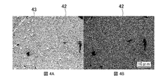
- FIG. 4A is an SEM image of the substrate used for the evaluation of the SPR sensor chip according to the first embodiment.
- FIG. 4A is an image before applying vibration
- FIG. 4B is an image after applying vibration.
- It is a graph which shows the evaluation result of the SPR sensor chip concerning a 1st embodiment.
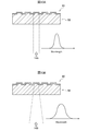
- FIG. 13A is a schematic diagram for explaining the usage state of the SPR sensor chip according to the modification.
- FIG. 13A shows incident light with a wavelength or incident angle selected
- FIG. 13B shows incident light with no wavelength or incident angle selected.
- FIG. 14A is a graph corresponding to FIG. 13A
- FIG. 14B is a graph corresponding to FIG. 13B.
- the SPR sensor chip according to the present invention is provided with a base portion formed of silicon (Si), an SPR portion that is provided on the surface of the base portion and generates plasmon resonance by incident incident light, and is provided on the base portion.
- a debonding unit that imparts mechanical energy to the SPR unit.
- the SPR sensor chip can desorb the detection target substance bonded to the surface of the SPR part by applying physical energy to the SPR part. Therefore, since the SPR sensor chip can desorb the detection target substance faster than the conventional one, a quicker response is possible accordingly.
- the SPR sensor chip includes a case where incident light is incident from the back surface side of the base portion and a case where the light is incident from the front surface side with respect to the SPR portion provided on the surface of the base portion.
- the case where incident light enters from the back side of the base includes the case where a prism is provided on the back side of the base and the case where the SPR part has a grating structure.
- the incident light is not particularly limited when incident from the surface of the base, and when incident from the back side of the base, it is preferable to use infrared light that passes through the base formed of silicon (Si). Even when the light is incident from the back side of the base, visible light can be used as incident light by setting the thickness of the base to a predetermined thickness or less.
- the SPR sensor includes an SPR sensor chip, a light emitting unit that irradiates the incident light toward the SPR unit, and a detection unit that detects an SPR response.
- the detection unit includes a case where the SPR response is acquired electrically and a case where the SPR response is acquired optically.
- Glucose and ions can be applied as the detection target substance. Further, a taste substance can be applied as the detection target substance.
- Taste substances refer to chemical substances that humans and animals can recognize as tastes, and there are types such as salty taste, sour taste, sweet taste, bitter taste, and umami taste.
- Physical energy includes at least one of mechanical energy, thermal energy, electrical energy, and light energy. Specific examples include tension, compression, vibration, ultrasonic waves, surface acoustic waves, heating, electric fields, magnetic fields, electromagnetic waves (light), and the like.
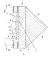
- the SPR sensor 10 shown in FIG. 1 includes an SPR sensor chip 12A, a light emitting unit 14, and a current detection unit 16 as a detection unit.
- the SPR sensor chip 12 ⁇ / b> A includes an SPR unit 18 and a coupling release unit 20.
- the SPR sensor 10 further includes a control unit 26 and an operation unit 28.
- the control unit 26 is electrically connected to the SPR sensor chip 12A, the light emitting unit 14, the current detection unit 16, and the operation unit 28.
- the control unit 26 reads application programs such as basic programs and arithmetic processing programs stored in advance, and controls the entire SPR sensor 10 according to these various programs.
- the control unit 26 can execute a plurality of programs (such as application programs) in parallel.
- the light emitting unit 14 is fixed to a base (not shown) and is optically connected to the SPR sensor chip 12A.
- the light emitting unit 14 receives the irradiation signal output from the control unit 26, the light emitting unit 14 irradiates the SPR unit 18 with infrared light at a constant incident angle.
- the infrared light emitted by the light emitting unit 14 is preferably light having a wavelength in the range of 1 ⁇ m to 10 ⁇ m that transmits Si.
- the light emitting unit 14 may be a laser diode or LED that emits monochromatic light. For example, use of a light source having a center wavelength of 1.31 ⁇ m or 1.55 ⁇ m is more preferable because the selection range of optical components is widened. .
- a chopper 22 may be provided between the light emitting unit 14 and the SPR sensor chip 12A.
- the chopper 22 receives the modulation signal output from the control unit 26, the chopper 22 periodically chops the light emitted from the light emitting unit 14, thereby alternately turning on and off and modulating the light.
- the light emitted from the light emitting unit 14 is incident on the SPR unit 18 in a state where the light amount is changed in a pulse shape by the chopper 22.
- the current detection unit 16 is electrically connected to the SPR sensor chip 12A, and detects the current value of the SPR unit 18 as an SPR response.
- the current detection unit 16 preferably has a lock-in amplifier 24 when the chopper 22 is used.
- the lock-in amplifier 24 can receive noise from the SPR response by receiving a reference signal synchronized with the chopping modulation signal from the control unit 26 and detecting a frequency component equal to the reference signal.
- the current detection unit 16 is electrically connected to the control unit 26.
- the current detection unit 16 generates a detection signal corresponding to the detected current value and outputs the detection signal to the control unit 26.
- the operation unit 28 includes an input unit 30 and a display unit 32.
- the input unit 30 may be any device that can input data, such as a touch panel and a keyboard. An operator can input characters, numbers, symbols, and the like using the input unit 30. When the input unit 30 is operated by an operator, the input unit 30 generates a signal corresponding to the operation. And the produced
- the display unit 32 may be any device as long as it can display images, images, and the like, and is, for example, a liquid crystal display or an organic EL (Electro-Luminescence) display.
- the display unit 32 displays detection values, graphs, and the like corresponding to the detection data supplied from the control unit 26.
- the display unit 32 may be an output device that prints video, images, characters, or the like on a display medium such as paper.
- the SPR sensor chip 12A will be described with reference to FIG.
- the SPR sensor chip 12A includes a base 34 made of silicon (Si). On the surface 36 of the base portion 34, the SPR portion 18 and the coupling release portion 20 are provided.
- a base 34 for example, n-type silicon doped with P (phosphorus) can be used.
- the doping amount of P is not particularly limited, but for example, it is preferably adjusted so that the resistivity of the base portion 34 is about 10 to 20 ⁇ cm.
- the base 34 is provided with an electrode 38 and is electrically connected to the current detection unit 16 through a wiring.
- the base portion 34 is integrally formed with a prism 35 on the back surface 37 side.
- An angle formed between the surface 36 and a back surface 37 (hereinafter also referred to as “incident surface”) facing the surface 36 is defined as an apex angle ⁇ . Since the critical angle is 22.3 degrees, in order to induce SPR, it is necessary to make light incident on the surface 36 at about 22.3 degrees. Therefore, it is most preferable to irradiate the light from the light emitting portion 14 in the direction perpendicular to the incident surface 37 having the apex angle ⁇ of 22.3 degrees because reflection of light at the incident surface 37 is minimized.
- the apex angle ⁇ is not limited to 22.3 degrees.
- the apex angle ⁇ is 5.6 degrees to 39.0 degrees, it is about 22 with respect to the surface 36 by adjusting the direction of the light emitted from the light emitting unit 14. SPR can be induced by making light incident at 3 degrees.
- the apex angle ⁇ is more preferably 14.3 degrees to 30.3 degrees because reflection of light at the incident surface 37 can be suppressed.
- the prism 35 may be a Fresnel lens type.
- the base 34 is not limited to the case where the prisms 35 are integrally formed.
- the base 34 may be integrally formed by fixing a glass prism to the back surface parallel to the front surface.
- the base portion 34 for example, after selectively forming a photoresist mask on the back surface 37, an incident surface is formed at a predetermined angle by anisotropic dry etching.
- the prism 35 can be integrally formed on the back surface 37 of the base portion 34 by removing the photoresist mask.
- the SPR unit 18 includes a metal layer 42 and a recognition layer 44 formed on the surface of the metal layer 42.
- the metal layer 42 is Schottky bonded to the surface 36, and is formed of, for example, gold (Au), silver (Ag), or copper (Cu).
- the thickness of the metal layer 42 is not particularly limited, but can be, for example, 50 nm to 200 nm.
- the metal layer 42 is provided with an electrode 39 and is electrically connected to the current detection unit 16 through a wiring.
- the base 34 and the metal layer 42 are connected in series through the wiring.
- the surface 36 is cleaned with hydrofluoric acid, a piranha solution, a surfactant, or the like, or plasma-treated with oxygen, and then the metal layer 42 is deposited by vapor deposition. 42 is formed. After vapor deposition, annealing is performed at 100 to 200 ° C. for 10 minutes to 3 hours. A good Schottky junction can be obtained by forming the metal layer 42 on the surface 36 by the above procedure.
- the electron barrier layer can be formed of titanium (Ti), molybdenum (Mo), or platinum (Pt).
- the thickness of the electron barrier layer is not particularly limited, but can be, for example, 1 nm to 10 nm.
- the recognition layer 44 specifically binds to the detection target substance 56 included in the sample 54.
- the recognition layer 44 can be a self-assembled film of phenylboronic acid-thiol (16-amino-1-hexadecanethiol, 10-carboxy-1-decanethiol) that binds to glucose.
- the self-assembled film can be formed on the surface of the metal layer 42 by immersing the metal layer 42 in a solution containing phenylboronic acid-thiol, for example.
- the bond release unit 20 desorbs the detection target substance 56 bonded to the recognition layer 44 by applying mechanical energy to the SPR unit 18.
- the coupling release unit 20 includes a piezoelectric body 50 that vibrates in the vertical direction (longitudinal direction) with respect to the surface of the SPR unit 18 and a pair of electrodes 48 provided on both sides in the thickness direction of the piezoelectric body 50. , 52 and is fixed to both sides of the SPR portion 18 of the surface 36 with an insulator 46 interposed therebetween.
- the piezoelectric body 50 can be formed by, for example, a piezo element or barium strontium titanate (Ba x Sr (1-x) TiO 3 ; BST, 0 ⁇ x ⁇ 1).
- the electrodes 48 and 52 are electrically connected to the control unit 26 through wiring, and vibrate in the thickness direction when a predetermined voltage is applied.
- the SPR sensor chip 12 ⁇ / b> A is irradiated with infrared light from the light emitting portion 14 disposed on the back surface 37 side of the base portion 34 toward the incident surface 37.
- the infrared light irradiated from the light emitting unit 14 passes through the prism 35 and enters the metal layer 42 as incident light. Incident light enters the surface 36 at an angle exceeding the critical angle and is totally reflected.
- the incident light generates an evanescent wave at the interface between the surface 36 and the metal layer 42, and free electrons in the metal layer 42 obtain energy from the evanescent wave, thereby inducing SPR, which is an electron density wave.
- SPR which is an electron density wave.
- the movement of the free electrons is detected by the current detector 16 as a current value. It is considered that the current value includes a current caused by electrons flowing from the metal layer 42 to the base 34 when the forward potential difference between the metal layer 42 and the base 34 exceeds a threshold due to SPR. .
- the sample 54 including the detection target substance 56 is brought into contact with the surface of the SPR portion 18.
- the detection target substance 56 contained in the sample 54 specifically binds to the recognition layer 44
- the dielectric constant of the recognition layer 44 changes.
- the resonance condition changes, and the movement of free electrons changes due to the decrease in the energy received.
- the current detection unit 16 detects a change in the movement of free electrons as a change in current value by the current detection unit 16, generates a detection signal, and inputs the detection signal to the control unit 26.
- the change in the current value includes a change in the current value flowing from the metal layer 42 to the base 34 due to a change in the potential difference between the metal layer 42 and the base 34 due to the change in the dielectric constant of the recognition layer 44. It is considered to be included.
- the control unit 26 analyzes the detection target substance 56 based on the detection signal and causes the display unit 32 to display the analysis result.
- the SPR sensor 10 can analyze the detection target substance 56 included in the sample 54 by detecting the change in the dielectric constant of the recognition layer 44 as a change in the current value by the current detection unit 16.
- the control unit 26 supplies a predetermined voltage to the piezoelectric body 50 and vibrates the piezoelectric body 50 in a state where the SPR unit 18 is immersed in a cleaning liquid (for example, water) as necessary.
- a cleaning liquid for example, water
- the vibration of the piezoelectric body 50 is transmitted to the SPR unit 18 through the base 34. Due to the vibration, the detection target substance 56 bonded to the recognition layer 44 is detached from the recognition layer 44.
- the SPR sensor 10 can analyze another sample by desorbing the detection target substance 56 from the recognition layer 44, further washing with water or the like as necessary, and drying.
- the SPR sensor 10 of the present embodiment can desorb the detection target substance faster than before by applying mechanical energy at the bond release unit 20, one analysis is completed accordingly. Therefore, it is possible to shorten the time until the next analysis is started and to analyze quickly.
- the SPR sensor 10 electrically detects the SPR response, an actuator for scanning the incident light can be omitted as compared with the case where it is optically detected.
- the SPR sensor 10 can electrically detect the SPR response with high efficiency because the metal layer 42 is Schottky bonded to the surface 36. By providing an electron barrier layer between the metal layer 42 and the surface 36, the SPR response can be detected more efficiently.
- the SPR sensor 10 can detect the SPR response more efficiently by modulating the light emitted from the light emitting unit 14 with the chopper 22 and removing the noise from the SPR response with the lock-in amplifier 24.
- Samples were prepared by the following procedure. First, Au nanoparticles having a diameter of 400 nm are immersed in a solution of 1 mM 10-carboxy-1-decanethiol dissolved in DMF (N, N-dimethylformamide) for 2 hours. Au particles coated with a carboxylic acid SAM (Self-Assembled Monolayer) were formed.
- An Au / Cr / glass wafer having a thickness of 200 nm / 5 nm / 400 ⁇ m was immersed in a solution of 1 mM 16-amino-1-hexadecanethiol in DMF for 2 hours to coat the amino acid SAM on the Au layer.
- a substrate was formed.
- a piezo element was attached to the bottom of the sample via a double-sided tape.
- the piezo element was driven at a frequency of 10 kHz to apply vibration.
- the input voltage to the piezo element was set to 5, 10, 15 kV for each sample, and after starting vibration, the density of Au particles was measured with SEM (Scanning Electron Microscope) at intervals of 10 seconds, 20 seconds, and 30 seconds. confirmed.
- SEM Sccanning Electron Microscope
- FIG. 4A is an image of the substrate surface before application of vibration, and the white dots recognized in the image are Au particles 43.
- FIG. 4B is an image at the same position on the substrate surface of the same sample as FIG. 4A after a voltage of 15 V is applied to the piezo element and vibration is applied for a total of 60 seconds. It was confirmed that the Au particles 43 on the substrate 42 decreased from 2.0 ⁇ 10 ⁇ 2 [pieces / ⁇ m 2 ] to 4.2 ⁇ 10 ⁇ 4 [pieces / ⁇ m 2 ] by applying the vibration. From this, it was confirmed that the molecules can be physically detached from the recognition layer by vibration.
- FIG. 5 shows the length of vibration time (s) on the horizontal axis and the residual ratio (%) of Au particles on the substrate on the vertical axis. According to this result, it was confirmed that the residual rate was reduced by applying vibration for at least 10 seconds or more, and the residual rate could be further reduced by increasing the input voltage.
- the coupling release unit 20 is fixed to both sides of the SPR unit 18 on the surface 36 via the insulator 46 , but the present invention is not limited to this.
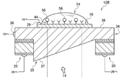
- the coupling release unit 20 of the SPR sensor chip 12B illustrated in FIG. 6 is fixed to the back surface 37 side.
- the SPR sensor chip 12B shown in this figure can obtain the same effect as that of the above embodiment by including the coupling release unit 20.
- the coupling release unit 20 may be provided on the surface 36 by sandwiching the piezoelectric body 50 between the electrodes 48 and 52 in parallel with the surface 36.
- the base 34 has been described with respect to the case where the prism 35 is formed on the back surface 37 side, but the present invention is not limited thereto.
- the SPR portion 60 of the SPR sensor chip 12C shown in FIG. 7 has a diffraction grating surface.
- concave portions 64 and convex portions 62 are alternately formed on the surface of the SPR portion 60 at a predetermined pitch.
- the concave portions 64 and the convex portions 62 are alternately formed on the surface 36
- the metal layer 65 is provided with a constant thickness along the surface 36
- the concave portions and the concave portions are provided on the surface of the metal layer 65. Protrusions are formed alternately.
- a recognition layer 44 is formed along the surface of the metal layer 65.
- the back surface 59 of the base portion 58 is not formed with a prism and is substantially parallel to the front surface 36.
- the SPR sensor chip 12C operates in the same manner as in the above embodiment. That is, the SPR unit 60 converts incident light into a near field on the diffraction grating surface and induces SPR. For example, a case where near infrared light having a wavelength of 1.55 ⁇ m is used will be described.
- the sample 54 is an aqueous solution
- the light emitting unit 14 irradiates the back surface 59 substantially perpendicularly, In order, the first-order diffracted light, second-order diffracted light, third-order diffracted light, and fourth-order diffracted light are combined with SPR to induce SPR.
- the sample 54 containing the detection target substance 56 is brought into contact with the surface of the SPR unit 60.
- the detection target substance 56 contained in the sample 54 specifically binds to the recognition layer 44, the dielectric constant of the recognition layer 44 changes. Then, the resonance condition changes, and the movement of free electrons changes due to the decrease in the energy received.
- the current detection unit 16 detects a change in the movement of free electrons as a change in current value by the current detection unit 16, generates a detection signal, and inputs the detection signal to the control unit 26.
- the SPR sensor can analyze the detection target substance 56 included in the sample 54 by detecting the change in the movement of free electrons as a change in the current value by the current detection unit 16. Since the SPR sensor chip 12C does not use the prism 35, the apparatus can be reduced in size and weight.
- the SPR sensor chip 12 ⁇ / b> D shown in FIG. 8 has a SAW (surface acoustic wave) oscillator 66 as the coupling release unit 20.
- the SAW oscillator 66 is an interdigital electrode, and is provided on the surface 36 of the base 34.
- the SAW oscillator 66 is electrically connected to the control unit 26, and generates a surface wave and applies mechanical energy to the SPR unit 18 when a predetermined voltage is applied.
- the SPR sensor chip 12D shown in this figure can obtain the same effect as that of the above embodiment by including the SAW oscillator 66.
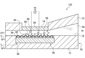
- the SPR sensor chip 12E shown in the figure includes a base portion 58, an SPR portion 60 having a diffraction grating surface, and a case 70.
- the case 70 includes a pedestal portion 71 that holds the base 58 and the SPR portion 60, and a flow path forming portion 73 that has a flow path 72 that leads to the surface of the SPR portion 60.
- the flow path 72 supplies the sample 54 to the surface of the SPR unit 60 by capillary action.
- the distance H between the inner wall of the flow path 72 and the surface of the SPR part 60 is preferably 1 mm or less.
- the flow path forming unit 73 can be formed of plastic, for example.
- the flow path forming unit 73 has an incident window 74 at a position corresponding to the SPR unit 60.
- the entrance window 74 has a glass plate fitted in a through hole provided in the ceiling portion of the flow path forming portion 73.
- the incident window 74 receives light emitted from the light emitting unit 14 disposed on the SPR unit 60 side.
- the distance H is preferably greater than 1 mm on the entrance side (“IN” in the figure), and the ceiling portion on the entrance side is SPR so that the distance H decreases linearly from the entrance side to the SPR unit 60. It is preferable to incline toward the portion 60. By inclining, the sample 54 can be moved to the surface of the SPR unit 60 more easily.
- the flow path 72 is provided with an ultrasonic transducer (not shown) as the coupling release unit 20.
- the ultrasonic vibrator applies ultrasonic waves to the sample 54 and the cleaning liquid flowing through the flow path 72.
- the surface of the SPR unit 60 is irradiated with light approximately perpendicularly to the SPR sensor chip 12E from the light emitting unit 14 disposed on the SPR unit 60 side.
- the light is not limited to infrared light, and may be visible light.
- the light is preferably monochromatic light.
- the light emitted from the light emitting unit 14 enters the SPR unit 60 through the incident window 74 and the flow path 72.
- the SPR unit 60 converts the incident light into a near field on the diffraction grating surface and induces SPR.
- the movement of free electrons in the metal layer 65 is detected by the current detection unit 16 as a current value.
- the sample 54 containing the detection target substance 56 is supplied to the flow path 72, and the sample 54 is brought into contact with the SPR unit 60.
- the detection target substance 56 contained in the sample 54 specifically binds to the recognition layer 44, the dielectric constant of the recognition layer 44 changes. Then, the resonance condition changes, and the movement of free electrons changes due to the decrease in the energy received.
- the SPR sensor can analyze the detection target substance 56 included in the sample 54 by detecting the change in the movement of free electrons as a change in the current value by the current detection unit 16.
- the control unit 26 After analyzing the detection target substance 56, the control unit 26 outputs a predetermined desorption signal to an ultrasonic transducer (not shown) in a state where the sample 54 in the flow path 72 is replaced with a cleaning liquid (for example, water) as necessary. Then, the vibrator is vibrated. The vibration is transmitted to the SPR unit 60 through the cleaning liquid. Due to the vibration, the detection target substance 56 bonded to the recognition layer 44 is detached from the recognition layer 44. The SPR sensor can analyze another sample 54 by desorbing the detection target substance 56 from the recognition layer 44 and further supplying water or the like to the flow path 72 to clean the SPR unit 60 as necessary. .
- a cleaning liquid for example, water
- the SPR sensor according to the present embodiment can desorb the detection target substance faster than before by applying mechanical energy to the SPR unit 60 via the cleaning liquid with an ultrasonic vibrator.
- the same effect as the form can be obtained.
- a piezoelectric body may be fixed to the flow path 72 in the vicinity of the SPR unit 60 as a coupling release unit.
- the SPR sensor chip 12E induces SPR by light irradiated to the SPR unit 60 from the SPR unit 60 side
- the SPR sensor chip 12E is not limited to infrared light, and various types of light can be used.
- the sample 54 can be more reliably supplied to the surface of the SPR unit 60 by capillary action.
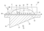
- the coupling release unit 76 of the SPR sensor chip 12 ⁇ / b> F shown in the figure includes an electrode 80 that generates an electric field between the metal layer 42.
- the electrode 80 is provided on the surface 36 at a predetermined distance from the metal layer 42.
- the metal layer 42 and the base 34 are electrically connected to the current detector.
- the recognition layer 81 of the SPR unit 18 can use an ion exchange membrane that adsorbs ions.
- an ion exchange membrane for example, Nafion (registered trademark), Flemion (registered trademark), Selemion (registered trademark), or the like can be used.
- the electrode 80 and the metal layer 42 are connected to a power source through wiring.
- a DC voltage between the electrode 80 and the metal layer 42 an electric field E is formed between the electrode 80 and the metal layer 42. Due to the electric field E, the detection target substance 56 bonded to the recognition layer 44 is detached from the recognition layer 81.
- the SPR sensor can analyze another sample 54 by desorbing the detection target substance 56 from the recognition layer 81 and further supplying water or the like as needed to wash the SPR unit 18. Since the SPR sensor chip 12F desorbs the detection target substance 56 bonded to the recognition layer 81 more quickly from the recognition layer 81 by the electric field E, the same effect as in the first embodiment can be obtained.
- the SPR sensor chip 12G shown in FIG. 11 is provided with an electrode 80 facing the SPR portion 18 with the flow path 77 interposed therebetween.
- the SPR sensor chip 12G has a flow path forming part 78 in which a flow path 77 leading to the surface of the SPR part 18 is formed.
- the electrode 80 is provided on the ceiling portion of the flow path forming portion 78 facing the SPR portion 18.
- the electrode 80 and the metal layer 42 are connected to a power source through wiring.
- an electric field E is formed between the electrode 80 and the metal layer 42 perpendicular to the flow path 77. Since the SPR sensor chip 12G desorbs the detection target substance 56 bound to the recognition layer 81 more quickly from the recognition layer 81 by the electric field E, the same effect as in the first embodiment can be obtained.
- the SPR sensor chip 12H shown in the figure includes a base portion 82 made of Si, an SPR portion 18 provided on the surface of the base portion 82, a coupling release portion 20, and a prism provided integrally on the back surface of the base portion 82. 84.
- the base 82 has a thickness T of at least a part of a portion in contact with the SPR portion 18 of 1 ⁇ m or less.
- the base portion 82 is formed with a hole 88 having a bottom portion 86 on the back surface side corresponding to the SPR portion 18.
- the thickness T of the bottom portion 86 is 1 ⁇ m or less.
- the hole 88 is filled with matching oil and is sealed by the prism 84.
- the matching oil preferably has a refractive index close to Si.
- the prism 84 is made of glass or plastic.
- the apex angle ⁇ of the prism 84 is preferably 30 to 60 degrees.
- the plastic for example, polyethylene, polypropylene, ABS resin, polyamide, and polycarbonate can be used.
- the SPR sensor chip 12H operates in the same manner as in the first embodiment.
- the SPR sensor chip 12H is irradiated with light from the light emitting unit 14 disposed on the back side of the base 82 at a constant incident angle.
- the light emitting unit 14 preferably emits light at 72 degrees with respect to a direction perpendicular to the surface 36.
- the portion of the Si base 82 that is in contact with the SPR portion 18 has a thickness T of 1 ⁇ m or less, and therefore transmits not only infrared light but also visible light. Therefore, the light emitted by the light emitting unit 14 is not limited to infrared light, and may be visible light.
- the infrared light emitted from the light emitting unit 14 sequentially passes through the incident surface 85 through the prism 84 and the matching oil, passes through the bottom 86 of the hole, and enters the metal layer 42 as incident light.
- Incident light enters the surface 36 at an angle exceeding the critical angle and is totally reflected.
- the incident light generates an evanescent wave at the interface between the surface 36 and the metal layer 42, and free electrons obtain energy from the evanescent wave, thereby inducing SPR.
- the detection target substance 56 contained in the sample 54 can be analyzed.
- the thickness of the Si base 34 is 1 ⁇ m or less, not only infrared light but also visible light is transmitted. Therefore, since the SPR sensor can make incident light incident on the SPR portion 18 from a portion having a thickness of 1 ⁇ m or less, the selectivity of the light emitting portion 14 can be expanded.
- the present invention is not limited to the above-described embodiment, and can be appropriately changed within the scope of the gist of the present invention.
- the incident light will be described with reference to FIGS. 13A and 13B and FIGS. 14A and 14B.
- symbol is attached
- the vertical axis represents the current value detected by the current detector 16
- the horizontal axis represents the incident angle or wavelength of the incident light.
- the light emitting unit 14 has been described with respect to irradiating monochromatic light.
- the relationship between the condition (incident angle or wavelength) ⁇ 1 of the incident light that becomes the resonance angle and the detected current value I 1 is a curve of n 1 .
- the light emitting unit 14 of the present modification emits broad infrared light including a plurality of incident angles or a plurality of wavelengths.
- the incident light condition shifts to ⁇ 2 and ⁇ 3 with respect to the incident light condition (incident angle or wavelength) ⁇ 1 as the resonance angle, the peak is gentle, so it is included in ⁇ 2 and ⁇ 3 .
- the light component of ⁇ 1 is larger than that of monochromatic light. Therefore, the current values I 4 and I 5 detected when the incident light condition is shifted to ⁇ 2 and ⁇ 3 are larger than the current values I 2 and I 3 in the case of monochromatic light.
- the incident light condition deviates from the resonance angle condition. Even if it exists, the detection target substance 56 can be analyzed more reliably. That is, in the case of this modification, the selectivity of detection conditions can be expanded.
- an antireflection film on the incident surface it is preferable to provide an antireflection film on the incident surface.
- the antireflection film on the incident surface reflection on the incident surface can be suppressed and conditions for inducing SPR can be easily obtained.
- a plurality of SPR sensor chips may be arranged in an array.
- a plurality of SPR portions are formed on a Si substrate, a prism is integrally formed on the back surface of the Si substrate by anisotropic dry etching, and cut into a predetermined size.
- mass productivity can be improved.
- mass productivity is improved by forming a plurality of SPR portions on a Si substrate, fixing a plastic prism on the back surface of the Si substrate, and cutting out to a predetermined size.
- SPR portions mass productivity is improved by forming a plurality of SPR portions on a Si substrate, fixing a plastic prism on the back surface of the Si substrate, and cutting out to a predetermined size.
- polyethylene, polypropylene, ABS resin, polyamide, and polycarbonate are excellent in releasability and are suitable for injection molding.
- the debonding unit may include an electric heater at the base, heat the SPR unit with the electric heater, and desorb the detection target substance from the recognition layer.
- the base may include a resin base and silicon fine particles dispersed in the resin base.
- a resin base can be formed by dispersing silicon fine particles in a resin and performing injection molding. Further, it can be formed by using an ultraviolet curable resin, dispersing silicon fine particles in the resin, and irradiating with ultraviolet rays.
- the base part according to the present modification can simplify the manufacturing process and reduce the cost as compared with the case where it is formed from a silicon substrate.
- the base may be formed of a medium having a specific high refractive index by a structure called a metamaterial.
- the metamaterial can be formed, for example, by diffusing fine particles of metal or high dielectric material.
- the size of the unit structure of the metamaterial is an order of magnitude smaller than the wavelength, it can be regarded as a homogeneous high refractive index material.
- control unit 26 and the operation unit 28 are provided has been described, the present invention is not limited thereto, and the control unit 26 and the operation unit 28 may be omitted as appropriate.
- the SPR sensor may be mounted on a robot, and in that case, the SPR sensor may be operated by a control unit and an operation unit of the robot.
Landscapes
- Chemical & Material Sciences (AREA)
- General Health & Medical Sciences (AREA)
- Life Sciences & Earth Sciences (AREA)
- Health & Medical Sciences (AREA)
- Analytical Chemistry (AREA)
- Biochemistry (AREA)
- Physics & Mathematics (AREA)
- General Physics & Mathematics (AREA)
- Immunology (AREA)
- Pathology (AREA)
- Chemical Kinetics & Catalysis (AREA)
- Electrochemistry (AREA)
- Investigating Or Analysing Materials By Optical Means (AREA)
- Investigating Or Analyzing Materials By The Use Of Electric Means (AREA)
Abstract
迅速に解析をすることができるSPRセンサチップ、SPRセンサ、及び試料の解析方法を提供する。SPRセンサチップ12Aは、シリコン(Si)で形成された基部34と、前記基部34の表面36に設けられ、入射された入射光によってプラズモン共鳴を発生するSPR部18と、物理的エネルギーを前記SPR部18に付与する結合解除部20とを備える。
Description
本発明は、SPRセンサチップ、SPRセンサ、及び試料の解析方法に関するものである。
表面プラズモン共鳴(SPR;Surface Plasmon Resonance)を利用するセンサの動作原理は、以下の通りである。例えば、プリズム型のSPRセンサの場合、プリズムを介して金属層に光を照射し、当該金属層の近傍において、エバネッセント波を発生させる。一方、金属層の表面には、光の照射により、同時に、表面プラズモンが発生する。所定の共鳴条件に合致すると、エバネッセント波と表面プラズモンとが共鳴し(すなわち表面プラズモン共鳴が発生し)、光の反射量が減少する。光の反射量が最小値となるときのプリズムと金属層の界面における入射角を共鳴角という。表面プラズモン共鳴における共鳴条件には、例えば、光の入射角、光の波長、金属層周囲の媒質の誘電率などの条件が含まれる。
そこで、センサ表面に特定の分子に特異的に反応する反応膜を設け、当該反応膜とデバイスとの界面に入射角度を変えながらレーザ光を照射し、反射光の強度を計測することによって、試料の分析を行う計測装置が開示されている(例えば特許文献1)。上記特許文献1では、反応膜と分子が吸着すると、媒質の誘電率が変化する。誘電率が変化すると共鳴角が変化するので、共鳴角の変化を検出することによって、特定の分子を検出することが可能となる。
しかし、従来は、化学的反応によって、反応膜に結合した分子を反応膜から脱離させていた。したがって分子を反応膜から脱離し、次の分子を検出可能とするために、長時間を要する。したがって、SPRセンサは、ロボットのように迅速な応答が求められる環境で使用することが難しいという問題があった。
本発明は、迅速に解析をすることができるSPRセンサチップ、SPRセンサ、及び試料の解析方法を提供することを目的とする。
本発明に係るSPRセンサチップは、シリコン(Si)で形成された基部と、前記基部の表面に設けられ、入射された入射光によってプラズモン共鳴を発生するSPR部と、物理的エネルギーを前記SPR部に付与する結合解除部とを備える。
本発明に係るSPRセンサは、上記SPRセンサチップと、前記SPR部へ向けて前記入射光を照射する発光部と、SPR応答を検出する検出部とを備える。
本発明に係る試料の解析方法は、入射された入射光によってプラズモン共鳴を発生するSPR部に試料を配置するステップと、前記SPR部へ向けて前記入射光を照射するステップと、SPR応答を検出するステップと、前記SPR部に物理的エネルギーを付与するステップとを有する。
本発明によれば、結合解除部で物理的エネルギーを付与することによって、従来に比べ速く検出対象物質を脱離することができるので、その分、1回の解析を終了してから、次の解析を開始するまでの時間を短縮し、迅速に解析することができる。
本発明に係るSPRセンサチップは、シリコン(Si)で形成された基部と、前記基部の表面に設けられ、入射された入射光によってプラズモン共鳴を発生するSPR部と、前記基部に設けられ、物理的エネルギーを前記SPR部に付与する結合解除部とを備える。SPRセンサチップは、物理的エネルギーを、SPR部に付与することによって、SPR部表面に結合した検出対象物質を脱離することができる。したがって、SPRセンサチップは、従来に比べ速く検出対象物質を脱離することができるので、その分、迅速な応答が可能である。
SPRセンサチップは、基部の表面に設けられたSPR部に対し、基部の裏面側から入射光が入射する場合と、表面側から入射する場合とを含む。基部の裏面側から入射光が入射する場合、基部の裏面側にプリズムが設けられている場合と、SPR部がグレーチング構造である場合とを含む。
入射光は、基部の表面から入射する場合は特に限定されず、基部の裏面側から入射する場合はシリコン(Si)で形成された基部を透過する赤外光を用いるのが好ましい。基部の裏面側から入射する場合であっても、基部の厚さを所定の厚さ以下とすることによって、入射光として可視光を用いることができる。
SPRセンサは、SPRセンサチップと、前記SPR部へ向けて前記入射光を照射する発光部と、SPR応答を検出する検出部とを備える。検出部は、SPR応答を、電気的に取得する場合と、光学的に取得する場合とを含む。
検出対象物質は、グルコースと、イオンを適用することができる。また、検出対象物質は、味物質を適用することもできる。味物質は、ヒトや動物が味覚として認識できる化学物質をいい、塩味、酸味、甘味、苦味、旨味などの種類がある。
物理的エネルギーとは、力学的エネルギー、熱エネルギー、電気エネルギー、及び光エネルギーの少なくとも一つを含む。具体的には、引張り、圧縮、振動、超音波、表面弾性波、加熱、電場、磁場、電磁波(光)などが挙げられる。
1.第1実施形態
(全体構成)
以下、図面を参照して本発明の第1実施形態について詳細に説明する。図1に示すSPRセンサ10は、SPRセンサチップ12Aと、発光部14と、検出部としての電流検出部16を備える。SPRセンサチップ12Aは、SPR部18と、結合解除部20とを有する。本実施形態の場合、SPRセンサ10は、さらに制御部26及び操作部28を備えている。
(全体構成)
以下、図面を参照して本発明の第1実施形態について詳細に説明する。図1に示すSPRセンサ10は、SPRセンサチップ12Aと、発光部14と、検出部としての電流検出部16を備える。SPRセンサチップ12Aは、SPR部18と、結合解除部20とを有する。本実施形態の場合、SPRセンサ10は、さらに制御部26及び操作部28を備えている。
制御部26は、SPRセンサチップ12A、発光部14、電流検出部16、操作部28と電気的に接続されている。制御部26は、予め格納されている基本プログラムや演算処理プログラム等のアプリケーションプログラムを読み出して、これら各種プログラムに従って、SPRセンサ10全体を制御する。制御部26は、複数のプログラム(アプリケーションプログラム等)を並列に実行できる。
発光部14は、図示しない基台に固定されており、SPRセンサチップ12Aと光学的に接続されている。発光部14は、制御部26が出力した照射信号を受け取ると、SPR部18へ向けて一定の入射角で赤外光を照射する。発光部14が照射する赤外光は、Siを透過する波長1μm~10μmの範囲の光であるのが好ましい。発光部14は、単色光を照射するレーザーダイオードや、LEDを用いることができ、例えば、中心波長が1.31μm、1.55μmの光源を用いると、光学部品の選択の幅が広がるのでより好ましい。
発光部14とSPRセンサチップ12Aの間にチョッパ22を設けてもよい。チョッパ22は、制御部26が出力した変調信号を受け取ると、発光部14から照射された光を周期的にチョッピングすることによって、点灯と消灯とを交互に繰り返し、変調する。発光部14から照射された光は、チョッパ22によって、光量がパルス状に変化した状態で、SPR部18へ入射する。
電流検出部16は、SPRセンサチップ12Aと電気的に接続されており、SPR応答としてSPR部18の電流値を検出する。電流検出部16は、チョッパ22を用いる場合、ロックインアンプ24を有するのが好ましい。ロックインアンプ24は、制御部26からチョッピングの変調信号に同期した参照信号を受け取り、参照信号と等しい周波数成分を検出することによって、SPR応答からノイズを除去することができる。電流検出部16は、制御部26と電気的に接続されている。電流検出部16は、検出した電流値に対応した検出信号を生成し、制御部26へ出力する。
操作部28は、入力部30と表示部32とを有する。入力部30は、データの入力が可能であればどのようなデバイスでもよく、例えば、タッチパネル、キーボード等である。作業者は、入力部30を用いて、文字、数字、記号等を入力することができる。入力部30は、作業者により操作されると、その操作に対応する信号を生成する。そして、生成された信号は、作業者の指示として、制御部26に入力される。
表示部32は、映像や画像等の表示が可能であればどのようなデバイスでもよく、例えば、液晶ディスプレイ又は有機EL(Electro-Luminescence)ディスプレイ等である。表示部32は、制御部26から供給された検出データに応じた検出値やグラフ等を表示する。また、表示部32は、紙等の表示媒体に、映像、画像又は文字等を印刷する出力装置であってもよい。
図2を参照してSPRセンサチップ12Aについて説明する。SPRセンサチップ12Aは、シリコン(Si)で形成された基部34を備える。当該基部34の表面36に、SPR部18と、結合解除部20とが設けられている。基部34は、例えばP(リン)がドープされたn型シリコンを用いることができる。Pのドープ量は特に制限されないが、例えば、基部34の抵抗率が10~20Ωcm程度になるように調整するのが好ましい。基部34は、電極38が設けられており、配線を通じて電流検出部16に電気的に接続されている。
基部34は、裏面37側にプリズム35が一体に形成されている。表面36と、前記表面36に対向した裏面(以下、「入射面」ともいう)37とのなす角度を頂角θとする。臨界角が22.3度であるので、SPRを誘起するため、表面36に対し約22.3度で光を入射させる必要がある。したがって頂角θが22.3度である入射面37に対し、垂直な方向に発光部14から光を照射するのが、入射面37での光の反射が最少となるので、最も好ましい。頂角θは、22.3度に限定されるものではなく、5.6度~39.0度であれば、発光部14が照射する光の方向を調整することによって表面36に対し約22.3度で光を入射させ、SPRを誘起することができる。頂角θは、14.3度~30.3度が、入射面37における光の反射を抑制できるので、より好ましい。プリズム35は、フレネルレンズ型でもよい。基部34は、プリズム35が一体に形成されている場合に限らず、例えばガラス製のプリズムを表面に対し平行な裏面に固定して、一体的に形成してもよい。
基部34を形成するには、例えば、裏面37にホトレジストマスクを選択的に形成した後、異方性ドライエッチングによって所定角度で入射面を形成する。次いで、ホトレジストマスクを除去することによって、基部34の裏面37にプリズム35を一体に形成することができる。
SPR部18は、金属層42と、金属層42表面に形成された認識層44とを有する。金属層42は、表面36とショットキー接合されており、例えば、金(Au)、銀(Ag)、銅(Cu)で形成される。金属層42の厚さは、特に制限されないが、例えば、50nm~200nmとすることができる。金属層42は、電極39が設けられており、配線を通じて電流検出部16に電気的に接続されている。配線を通じて、基部34と金属層42は、直列に接続されている。
金属層42と表面36をショットキー接合するには、例えば、表面36をフッ化水素酸、ピラニア溶液、又は界面活性剤などで洗浄、あるいは酸素でプラズマ処理をしてから、蒸着法によって金属層42を形成する。蒸着後、100~200℃で10分~3時間アニールする。上記の手順で表面36に金属層42を形成することによって、良好なショットキー接合が得られる。
金属層42と基部34の間に、電子障壁層(図示しない)を設けるのが好ましい。電子障壁層は、チタン(Ti)、モリブデン(Mo)、白金(Pt)で形成することができる。電子障壁層の厚さは、特に制限されないが、例えば、1nm~10nmとすることができる。
認識層44は、試料54に含まれる検出対象物質56と特異的に結合する。本実施形態の場合、認識層44は、グルコースと結合するフェニルボロン酸-チオール(16-amino-1-hexadecanethiol, 10-carboxy-1-decanethiol)の自己組織化膜を用いることができる。自己組織化膜は、例えば、フェニルボロン酸-チオールを含む溶液中に金属層42を浸漬することによって、金属層42の表面に形成することができる。
結合解除部20は、SPR部18に力学的エネルギーを付与することによって、認識層44に結合した検出対象物質56を脱離させる。本実施形態の場合、結合解除部20は、SPR部18表面に対し垂直方向(縦方向)に振動する圧電体50と、当該圧電体50の厚さ方向の両側に設けられた一対の電極48,52とを有し、絶縁体46を介して表面36のSPR部18を挟んで両側に固定されている。圧電体50は、例えば、ピエゾ素子や、チタン酸バリウムストロンチウム(BaxSr(1-x)TiO3;BST、0<x<1)で形成することができる。電極48,52は、配線を介して制御部26に電気的に接続されており、所定の電圧が印加されると厚さ方向に振動する。
(作用及び効果)
次に本実施形態のSPRセンサ10の作用及び効果を説明する。まずSPRセンサチップ12Aに対し、基部34の裏面37側に配置された発光部14から、入射面37へ向かって赤外光を照射する。発光部14から照射された赤外光は、プリズム35を透過して入射光として金属層42に入射する。入射光は、臨界角を超える角度で表面36に入射し、全反射する。当該入射光によって表面36と金属層42の界面にエバネッセント波が発生し、当該エバネッセント波から金属層42中の自由電子がエネルギーを得ることによって、電子の粗密波であるSPRが誘起される。上記自由電子の動きを、電流値として電流検出部16で検出する。上記電流値には、SPRによって、金属層42と基部34との間の順方向の電位差が閾値を超えた場合に、金属層42から基部34へ電子が流れることによる電流も含まれると考えられる。
次に本実施形態のSPRセンサ10の作用及び効果を説明する。まずSPRセンサチップ12Aに対し、基部34の裏面37側に配置された発光部14から、入射面37へ向かって赤外光を照射する。発光部14から照射された赤外光は、プリズム35を透過して入射光として金属層42に入射する。入射光は、臨界角を超える角度で表面36に入射し、全反射する。当該入射光によって表面36と金属層42の界面にエバネッセント波が発生し、当該エバネッセント波から金属層42中の自由電子がエネルギーを得ることによって、電子の粗密波であるSPRが誘起される。上記自由電子の動きを、電流値として電流検出部16で検出する。上記電流値には、SPRによって、金属層42と基部34との間の順方向の電位差が閾値を超えた場合に、金属層42から基部34へ電子が流れることによる電流も含まれると考えられる。
この状態において、SPR部18表面に検出対象物質56を含む試料54を接触させる。試料54に含まれる検出対象物質56が認識層44と特異的に結合することによって、認識層44の誘電率が変化する。そうすると共鳴条件が変化し、自由電子は受け取るエネルギーが減少することによって動きが変化する。電流検出部16は、自由電子の動きの変化を電流値の変化として電流検出部16で検出し、検出信号を生成して制御部26に入力する。上記電流値の変化には、認識層44の誘電率の変化に起因して金属層42と基部34との間の電位差が変化することによって、金属層42から基部34へ流れる電流値の変化も含まれると考えられる。
制御部26は、検出信号に基づき、検出対象物質56を解析し、解析結果を表示部32に表示させる。SPRセンサ10は、認識層44の誘電率の変化を電流値の変化として電流検出部16で検出することによって、試料54に含まれる検出対象物質56を解析することができる。
検出対象物質56の解析後、必要に応じ洗浄液(例えば水)にSPR部18を浸漬した状態で、制御部26は、圧電体50に所定の電圧を供給し、圧電体50を振動させる。圧電体50の振動は、基部34を通じてSPR部18へ伝達される。当該振動によって、認識層44に結合された検出対象物質56が、認識層44から脱離する。SPRセンサ10は、認識層44から検出対象物質56を脱離させ、さらに必要に応じ水などで洗浄後、乾燥することによって、別の試料を解析することができる。
本実施形態のSPRセンサ10は、結合解除部20で機械的エネルギーを付与することによって、従来に比べ速く検出対象物質を脱離することができるので、その分、1回の解析を終了してから、次の解析を開始するまでの時間を短縮し、迅速に解析することができる。
SPRセンサ10は、SPR応答を電気的に検出するので、光学的に検出する場合に比べ、入射光を走査するためのアクチュエータを省略できるから、小型化を実現できる。
SPRセンサ10は、金属層42が表面36にショットキー接合されていることによって、SPR応答を電気的に高効率で検出することができる。金属層42と表面36との間に電子障壁層を設けることによって、より効率的にSPR応答を検出することができる。
SPRセンサ10は、発光部14から照射された光を、チョッパ22によって変調し、ロックインアンプ24でSPR応答からノイズを除去することによって、さらに効率的にSPR応答を検出することができる。
実際にサンプルを作製し、検出対象物質56を認識層44から脱離できることを検証した。サンプルは、以下の手順で作製した。まず1mMの10-カルボキシ-1-デカンチオールをDMF(N,N-ジメチルホルムアミド;N,N-dimethylformamide)に溶解した溶液に、直径400nmのAuナノ粒子を2時間浸漬して、Auナノ粒子にカルボン酸SAM(Self-Assembled Monolayer:自己組織化材料)をコーティングしたAu粒子を形成した。
1mMの16-アミノ-1-ヘキサデカンチオールをDMFに溶解した溶液に、200nm/5nm/400μmの厚さを有するAu/Cr/ガラスウェーハを2時間浸漬して、Au層上にアミノ酸SAMをコーティングした基板を形成した。
MES(エタンスルホン酸メチル;Methyl ethylsulfonate)バッファ(pH6.0)に4mMのEDC(エチレンジクロリド;Ethylenedichloride)と1mMのNHS(N-ヒドロキシスクシンイミド;N-Hydroxysuccinimide)とを加えた溶液中に、上記Au粒子と、上記基板を1時間浸漬し、Au粒子43を基板上のアミノ酸SAM44に結合させた(図3)。上記の手順により、3個のサンプルを得た。
上記サンプルの底面に両面テープを介してピエゾ素子を取り付けた。基板表面に20μlの純水を滴下した状態で、10kHzの周波数でピエゾ素子を駆動し、振動を印加した。ピエゾ素子への入力電圧は、サンプルごとに5,10,15kVとし、振動を開始後、10秒、20秒、30秒間隔でAu粒子の密度をSEM(走査型電子顕微鏡;Scanning Electron Microscope)で確認した。その結果を図4A,4B、及び図5に示す。
図4Aは、振動を印加する前の基板表面の画像であり、同画像に認められる白い点がAu粒子43である。図4Bは、ピエゾ素子に15Vの電圧を入力し、合計60秒間、振動を印加した後の図4Aと同じサンプルの基板表面の同じ位置における画像である。振動を印加することによって基板42上のAu粒子43は、2.0×10⁻²[個/μm2]から4.2×10-4[個/μm2]に減少したことが確認できた。このことから、振動によって分子を物理的に認識層から脱離できることが確認された。
図5は、横軸が振動時間の長さ(s)、縦軸が基板におけるAu粒子の残留率(%)を示している。本結果によれば、少なくとも10秒以上、振動を付与することで残留率が低減し、入力電圧を大きくすることで残留率をより低下できることが確認された。
(変形例)
上記実施形態の場合、結合解除部20は、絶縁体46を介して表面36のSPR部18を挟んで両側に固定されている場合について説明したが、本発明はこれに限らない。例えば、図6に示すSPRセンサチップ12Bの結合解除部20は、裏面37側に固定されている。本図に示すSPRセンサチップ12Bは、結合解除部20を備えることによって、上記実施形態と同様の効果を得ることができる。また結合解除部20は、表面36に平行に圧電体50を電極48,52で挟んで、表面36に設けてもよい。
上記実施形態の場合、結合解除部20は、絶縁体46を介して表面36のSPR部18を挟んで両側に固定されている場合について説明したが、本発明はこれに限らない。例えば、図6に示すSPRセンサチップ12Bの結合解除部20は、裏面37側に固定されている。本図に示すSPRセンサチップ12Bは、結合解除部20を備えることによって、上記実施形態と同様の効果を得ることができる。また結合解除部20は、表面36に平行に圧電体50を電極48,52で挟んで、表面36に設けてもよい。
上記実施形態の場合、基部34は、裏面37側にプリズム35が形成されている場合について説明したが、本発明はこれに限らない。例えば、図7に示すSPRセンサチップ12CのSPR部60は、回折格子面を有する。回折格子面は、SPR部60の表面に、凹部64と凸部62が交互に、かつ、所定のピッチで形成されている。本実施形態の場合、表面36に、凹部64と凸部62とが交互に形成されており、当該表面36に沿って金属層65が一定の厚さで設けられ、金属層65表面に凹部と凸部が交互に形成されている。金属層65表面に沿って、認識層44が形成されている。基部58の裏面59は、プリズムが形成されておらず、表面36に略平行である。
SPRセンサチップ12Cは、上記実施形態と同様に動作をする。すなわち、SPR部60は、回折格子面において入射光を近接場化し、SPRを誘起する。例えば波長1.55μmの近赤外光を利用する場合について説明する。試料54が水溶液であれば、回折格子面の周期を1.17μm、2.34μm、3.50μm、4.67μmとしたときに、発光部14が裏面59に対し略垂直に照射することによって、順に、1次回折光、2次回折光、3次回折光、4次回折光がSPRと結合し、SPRが誘起される。
この状態でSPR部60表面に検出対象物質56を含む試料54を接触させる。試料54に含まれる検出対象物質56が認識層44と特異的に結合することによって、認識層44の誘電率が変化する。そうすると共鳴条件が変化し、自由電子は受け取るエネルギーが減少することによって動きが変化する。電流検出部16は、自由電子の動きの変化を電流値の変化として電流検出部16で検出し、検出信号を生成して制御部26に入力する。SPRセンサは、自由電子の動きの変化を電流値の変化として電流検出部16で検出することによって、試料54に含まれる検出対象物質56を解析することができる。SPRセンサチップ12Cは、プリズム35を用いないため、装置の小型化、軽量化を実現することができる。
上記実施形態の場合、結合解除部20の圧電体50は、SPR部18表面に対し垂直方向(縦方向)に振動する場合について説明したが、本発明はこれ限らない。図8に示すSPRセンサチップ12Dは、結合解除部20としてSAW(弾性表面波;surface acoustic wave)発振子66を有する。SAW発振子66は、すだれ状電極であり、基部34の表面36に設けられている。SAW発振子66は、制御部26に電気的に接続されており、所定の電圧が印加されると、表面波を発生させ、SPR部18に力学的エネルギーを付与する。本図に示すSPRセンサチップ12Dは、SAW発振子66を備えることによって、上記実施形態と同様の効果を得ることができる。
2.第2実施形態
図9を参照して第2実施形態について説明する。なお、上記第1実施形態と同様の構成については同様の符号を付し、説明を省略する。本図に示すSPRセンサチップ12Eは、基部58と、回折格子面を有するSPR部60と、ケース70とを備える。ケース70は、基部58とSPR部60とを保持する台座部71と、SPR部60表面へ通じる流路72を有する流路形成部73とを有する。
図9を参照して第2実施形態について説明する。なお、上記第1実施形態と同様の構成については同様の符号を付し、説明を省略する。本図に示すSPRセンサチップ12Eは、基部58と、回折格子面を有するSPR部60と、ケース70とを備える。ケース70は、基部58とSPR部60とを保持する台座部71と、SPR部60表面へ通じる流路72を有する流路形成部73とを有する。
流路72は、毛細管現象によって試料54をSPR部60表面に供給する。流路72内壁とSPR部60表面との間の距離Hは、1mm以下であるのが好ましい。流路形成部73は、例えば、プラスチックで形成することができる。流路形成部73は、SPR部60に対応した位置に入射窓74を有する。入射窓74は、流路形成部73の天井部分に設けられた貫通穴にガラス板がはめ込まれている。入射窓74は、SPR部60側に配置された発光部14から照射された光を受け入れる。距離Hは、入口側(図中、「IN」)が1mm超であるのが好ましく、入口側からSPR部60へ向かって距離Hが直線的に小さくなるように、入口側の天井部分がSPR部60へ向かって傾斜しているのが好ましい。傾斜していることによって、より容易にSPR部60の表面へ試料54を移動させることができる。
流路72には、結合解除部20としての超音波振動子(図示しない)が設けられている。超音波振動子は、流路72を流れる試料54や洗浄液に超音波を付与する。
次に本実施形態のSPRセンサの作用及び効果を説明する。まずSPRセンサチップ12Eに対し、SPR部60側に配置された発光部14から、SPR部60表面に略垂直に光を照射する。当該光は、赤外光に限定されず、可視光でもよい。光は、単色光であるのが好ましい。発光部14が照射した光は、入射窓74、流路72を通じてSPR部60へ入射する。SPR部60は、回折格子面において当該入射光を近接場化し、SPRを誘起する。金属層65中の自由電子の動きを、電流値として電流検出部16で検出する。
この状態において、流路72に検出対象物質56を含む試料54を供給し、当該試料54をSPR部60に接触させる。試料54に含まれる検出対象物質56が認識層44と特異的に結合することによって、認識層44の誘電率が変化する。そうすると共鳴条件が変化し、自由電子は受け取るエネルギーが減少することによって動きが変化する。SPRセンサは、自由電子の動きの変化を電流値の変化として電流検出部16で検出することによって、試料54に含まれる検出対象物質56を解析することができる。
検出対象物質56の解析後、流路72内の試料54を、必要に応じ洗浄液(例えば水)に入れ替えた状態で、制御部26は、図示しない超音波振動子に所定の脱離信号を出力し、振動子を振動させる。当該振動は、洗浄液を通じてSPR部60へ伝達される。当該振動によって、認識層44に結合された検出対象物質56が、認識層44から脱離する。SPRセンサは、認識層44から検出対象物質56を脱離させ、さらに必要に応じ流路72に水などを供給してSPR部60を洗浄することによって、別の試料54を解析することができる。
本実施形態のSPRセンサは、超音波振動子で洗浄液を介してSPR部60に機械的エネルギーを付与することによって、従来に比べ速く検出対象物質を脱離することができるので、上記第1実施形態と同様の効果が得られる。なお、SPR部60近傍の流路72に結合解除部として圧電体を固定してもよい。
SPRセンサチップ12Eは、SPR部60側からSPR部60へ照射した光によってSPRを誘起するので、赤外光に限定されず、種々の光を用いることができる。SPRセンサチップ12Eは、入口側の天井部分がSPR部60へ向かって傾斜しているので、毛細管現象によってより確実に試料54をSPR部60表面に供給することができる。
3.第3実施形態
図10を参照して第3実施形態について説明する。なお、上記第1実施形態と同様の構成については同様の符号を付し、説明を省略する。本図に示すSPRセンサチップ12Fの結合解除部76は、金属層42との間に電場を発生させる電極80を備える。電極80は、金属層42と所定の距離をあけて、表面36に設けられている。本図には図示していないが、金属層42及び基部34は、電流検出部に電気的に接続されている。
図10を参照して第3実施形態について説明する。なお、上記第1実施形態と同様の構成については同様の符号を付し、説明を省略する。本図に示すSPRセンサチップ12Fの結合解除部76は、金属層42との間に電場を発生させる電極80を備える。電極80は、金属層42と所定の距離をあけて、表面36に設けられている。本図には図示していないが、金属層42及び基部34は、電流検出部に電気的に接続されている。
SPR部18の認識層81は、イオンを吸着するイオン交換膜を用いることができる。イオン交換膜としては、例えば、Nafion(登録商標)、フレミオン(登録商標)、セレミオン(登録商標)などを用いることができる。
電極80と金属層42は、配線を通じて電源に接続されている。電極80と金属層42の間に直流電圧を印加することによって、電極80と金属層42の間に電場Eが形成される。当該電場Eによって、認識層44に結合された検出対象物質56が、認識層81から脱離する。SPRセンサは、認識層81から検出対象物質56を脱離させ、さらに必要に応じ水などを供給してSPR部18を洗浄することによって、別の試料54を解析することができる。SPRセンサチップ12Fは、電場Eによって、認識層81に結合された検出対象物質56を認識層81からより速く脱離させるので、上記第1実施形態と同様の効果が得られる。
上記第3実施形態の場合、電極80は表面36に設ける場合について説明したが、本発明はこれに限らない。例えば、図11に示すSPRセンサチップ12Gは、流路77を挟んで、SPR部18に対向して電極80が設けられている。SPRセンサチップ12Gは、SPR部18表面へ通じる流路77が形成された流路形成部78を有する。電極80は、SPR部18に対向した流路形成部78の天井部分に設けられている。電極80と金属層42は、配線を通じて電源に接続されている。電極80と金属層42の間に直流電圧を印加することによって、流路77に直交して、電極80と金属層42の間に電場Eが形成される。SPRセンサチップ12Gは、電場Eによって、認識層81に結合された検出対象物質56を認識層81からより速く脱離させるので、上記第1実施形態と同様の効果が得られる。
4.第4実施形態
図12を参照して第4実施形態について説明する。なお、上記第1実施形態と同様の構成については同様の符号を付し、説明を省略する。本図に示すSPRセンサチップ12Hは、Siで形成された基部82と、基部82の表面に設けられたSPR部18と、結合解除部20と、基部82の裏面に一体的に設けられたプリズム84とを備える。
図12を参照して第4実施形態について説明する。なお、上記第1実施形態と同様の構成については同様の符号を付し、説明を省略する。本図に示すSPRセンサチップ12Hは、Siで形成された基部82と、基部82の表面に設けられたSPR部18と、結合解除部20と、基部82の裏面に一体的に設けられたプリズム84とを備える。
基部82は、SPR部18と接している部分の少なくとも一部の厚さTが1μm以下である。本図の場合、基部82は、SPR部18に対応した裏面側に底部86を有する穴88が形成されている。当該底部86の厚さTが1μm以下である。
当該穴88は、マッチングオイルが充填されており、プリズム84によって密閉されている。マッチングオイルは、Siに近い屈折率を有するのが好ましい。プリズム84は、ガラスやプラスチックで形成される。プリズム84の頂角θは、30度~60度であるのが好ましい。プラスチックとしては、例えば、ポリエチレン、ポリプロピレン、ABS樹脂、ポリアミド、ポリカーボネイトを用いることができる。
SPRセンサチップ12Hは、上記第1実施形態と同様に動作をする。まずSPRセンサチップ12Hに対し、基部82の裏面側に配置された発光部14から、一定の入射角で光を照射する。発光部14は、表面36に垂直な方向に対し72度で光を照射するのが好ましい。Siの基部82のSPR部18と接している部分は、厚さTが1μm以下であるので、赤外光だけでなく、可視光も透過する。したがって発光部14が照射する光は、赤外光に限定されず、可視光でもよい。
発光部14から照射された赤外光は、入射面85から、プリズム84、及びマッチングオイルを順に透過し、穴の底部86を透過して入射光として金属層42に入射する。入射光は、臨界角を超える角度で表面36に入射し、全反射する。当該入射光によって表面36と金属層42の界面にエバネッセント波が発生し、当該エバネッセント波から自由電子がエネルギーを得ることによって、SPRが誘起される。上記自由電子の動きを電流値として電流検出部16で検出することによって、試料54に含まれる検出対象物質56を解析することができる。
Siの基部34は、厚さが1μm以下であれば、赤外光だけでなく、可視光も透過する。したがってSPRセンサは、厚さが1μm以下の部分からSPR部18へ入射光を入射させることができるので、発光部14の選択性を広げることができる。
5.変形例
本発明は上記実施形態に限定されるものではなく、本発明の趣旨の範囲内で適宜変更することが可能である。
本発明は上記実施形態に限定されるものではなく、本発明の趣旨の範囲内で適宜変更することが可能である。
図13A,13B、及び図14A,14Bを参照して入射光について説明する。なお、上記第1実施形態と同様の構成については同様の符号を付し、説明を省略する。図14A,14Bは、縦軸が電流検出部16で検出される電流値、横軸が入射光の入射角又は波長を示している。上記実施形態の場合、図13Aに示すように、発光部14は、単色光を照射する場合について説明した。この場合の共鳴角となる入射光の条件(入射角又は波長)θ1と検出された電流値I1の関係をn1の曲線とする。これに対し入射光の条件がθ2、にずれた場合、入射光のピークが急峻なため、当該入射光に含まれるθ1の光成分が少なく、検出される電流値は、I2に低下してしまう。入射光の条件がθ3にずれた場合、検出される電流値はさらにI3に低下してしまう。
これに対し、図13Bに示すように、本変形例の発光部14は、複数の入射角、又は複数の波長を含むブロードな赤外光を照射する。この場合、共鳴角となる入射光の条件(入射角又は波長)θ1に対し、入射光の条件がθ2、θ3にずれても、ピークがゆるやかなため、θ2、θ3に含まれるθ1の光成分が単色光に比べ多い。したがって、入射光の条件がθ2、θ3にずれた場合に検出される電流値I4、I5は、単色光の場合の電流値I2、I3に比べ、大きい。
発光部14から入射角を変えずに光を照射する場合、複数の入射角、又は複数の波長を含むブロードな光を用いることによって、入射光の条件が共鳴角となる条件からずれた場合であっても、より確実に検出対象物質56を解析することができる。すなわち本変形例の場合、検出条件の選択性を広げることができる。
上記第1、第3、第4実施形態の場合において、入射面に反射防止膜を設けるのが好ましい。反射防止膜を入射面に設けることによって、入射面における反射を抑制し、SPRを誘起させる条件を容易に出すことができる。
上記実施形態において、SPRセンサチップを複数アレイ状に配列してもよい。第1~第3実施形態の場合、Si基板上に複数のSPR部を形成し、当該Si基板の裏面に異方性ドライエッチングによってプリズムを一体に形成し、所定のサイズに切り出して作製することによって、量産性を向上することができる。
第4実施形態の場合、Si基板上に複数のSPR部を形成し、当該Si基板の裏面にプラスチック製のプリズムを固定し、所定のサイズに切り出して作製することによって、量産性を向上することができる。特にポリエチレン、ポリプロピレン、ABS樹脂、ポリアミド、ポリカーボネイトは離形性に優れるので、射出成型に適している。
結合解除部は、電熱ヒータを基部に設け、当該電熱ヒータによってSPR部を加熱し、認識層から検出対象物質を脱離することとしてもよい。
基部は、樹脂ベースと、当該樹脂ベースに分散しているシリコンの微粒子とを含むこととしてもよい。このような基部は、樹脂中にシリコン微粒子を分散させて、射出成型をすることによって形成することができる。また紫外線硬化樹脂を用いて、当該樹脂中にシリコン微粒子を分散させて、紫外線を照射することによって形成することができる。本変形例に係る基部は、シリコン基板から形成するよりも、製造工程を簡略化でき、コストを低減することができる。
基部は、メタマテリアルと呼ばれる構造体によって、特定の高屈折率を有する媒質で形成してもよい。メタマテリアルは、例えば、金属または高誘電体の微粒子を拡散させて形成することができる。メタマテリアルの単位構造の大きさが波長より1桁小さい場合、均質な高屈折率材料とみなすことができる。
制御部26及び操作部28を備えている場合について説明したが、本発明はこれに限らず、制御部26及び操作部28は適宜省略してよい。例えば、SPRセンサは、ロボットに搭載してもよく、その場合は、ロボットの制御部及び操作部によって、動作することとしてもよい。
θ 頂角
10 SPRセンサ
12A~12H SPRセンサチップ
14 発光部
16 電流検出部(検出部)
18、60 SPR部
20、76 結合解除部
34、58、82 基部
35、84 プリズム
36 表面
37 裏面
54 試料
56 検出対象物質
72 流路
73 流路形成部
74 入射窓
10 SPRセンサ
12A~12H SPRセンサチップ
14 発光部
16 電流検出部(検出部)
18、60 SPR部
20、76 結合解除部
34、58、82 基部
35、84 プリズム
36 表面
37 裏面
54 試料
56 検出対象物質
72 流路
73 流路形成部
74 入射窓
Claims (7)
- シリコン(Si)で形成された基部と、
前記基部の表面に設けられ、入射された入射光によってプラズモン共鳴を発生するSPR部と、
物理的エネルギーを前記SPR部に付与する結合解除部と
を備えるSPRセンサチップ。 - 前記基部は、前記表面と、前記表面に対向した裏面とのなす角度が、5.6度~39.0度のプリズムである請求項1記載のSPRセンサチップ。
- 前記SPR部は、表面に、凹部と凸部が交互に、かつ、所定のピッチで形成された、回折格子面を有する請求項1記載のSPRセンサチップ。
- 前記SPR部と接している前記基部の厚さが1μm以下である請求項1記載のSPRセンサチップ。
- 前記SPR部表面へ通じる流路を有する流路形成部を備え、
前記流路形成部は、前記入射光を受け入れる入射窓を有する
請求項1記載のSPRセンサチップ。 - 請求項1~5のいずれか1項記載のSPRセンサチップと、
前記SPR部へ向けて前記入射光を照射する発光部と、
SPR応答を検出する検出部と
を備えるSPRセンサ。 - 入射された入射光によってプラズモン共鳴を発生するSPR部に試料を配置するステップと、
前記SPR部へ向けて前記入射光を照射するステップと、
SPR応答を検出するステップと、
前記SPR部に物理的エネルギーを付与するステップと
を有する試料の解析方法。
Applications Claiming Priority (2)
| Application Number | Priority Date | Filing Date | Title |
|---|---|---|---|
| JP2018-072599 | 2018-04-04 | ||
| JP2018072599A JP6954626B2 (ja) | 2018-04-04 | 2018-04-04 | Sprセンサチップ、sprセンサ、及び試料の解析方法 |
Publications (1)
| Publication Number | Publication Date |
|---|---|
| WO2019194166A1 true WO2019194166A1 (ja) | 2019-10-10 |
Family
ID=68100304
Family Applications (1)
| Application Number | Title | Priority Date | Filing Date |
|---|---|---|---|
| PCT/JP2019/014598 Ceased WO2019194166A1 (ja) | 2018-04-04 | 2019-04-02 | Sprセンサチップ、sprセンサ、及び試料の解析方法 |
Country Status (2)
| Country | Link |
|---|---|
| JP (1) | JP6954626B2 (ja) |
| WO (1) | WO2019194166A1 (ja) |
Cited By (1)
| Publication number | Priority date | Publication date | Assignee | Title |
|---|---|---|---|---|
| WO2021255396A1 (fr) * | 2020-06-19 | 2021-12-23 | Commissariat A L'energie Atomique Et Aux Energies Alternatives | Capteur environnemental immergé intégrant des moyens anti-encrassement |
Families Citing this family (2)
| Publication number | Priority date | Publication date | Assignee | Title |
|---|---|---|---|---|
| US12203860B2 (en) | 2021-10-05 | 2025-01-21 | Electronics And Telecommunications Research Institute | Biosensor device |
| KR102849466B1 (ko) * | 2021-10-05 | 2025-08-25 | 한국전자통신연구원 | 바이오센서 장치 |
Citations (5)
| Publication number | Priority date | Publication date | Assignee | Title |
|---|---|---|---|---|
| EP1566627A1 (en) * | 2004-02-18 | 2005-08-24 | Max-Planck-Gesellschaft zur Förderung der Wissenschaften e.V. | Surface plasmon field-enhanced diffraction sensor |
| JP2007248253A (ja) * | 2006-03-15 | 2007-09-27 | Omron Corp | 光学部品、光学センサ、表面プラズモンセンサ及び指紋認証装置 |
| JP2008057980A (ja) * | 2006-08-29 | 2008-03-13 | Sharp Corp | 分子検出装置及び分子検出装置を用いた洗浄装置 |
| JP2008089495A (ja) * | 2006-10-04 | 2008-04-17 | Sharp Corp | 分子検出センサ洗浄機能を備えた分子検出装置及び洗浄装置 |
| JP2010190778A (ja) * | 2009-02-19 | 2010-09-02 | Sangaku Renkei Kiko Kyushu:Kk | 飲料製造ラインの異臭検出システム |
-
2018
- 2018-04-04 JP JP2018072599A patent/JP6954626B2/ja active Active
-
2019
- 2019-04-02 WO PCT/JP2019/014598 patent/WO2019194166A1/ja not_active Ceased
Patent Citations (5)
| Publication number | Priority date | Publication date | Assignee | Title |
|---|---|---|---|---|
| EP1566627A1 (en) * | 2004-02-18 | 2005-08-24 | Max-Planck-Gesellschaft zur Förderung der Wissenschaften e.V. | Surface plasmon field-enhanced diffraction sensor |
| JP2007248253A (ja) * | 2006-03-15 | 2007-09-27 | Omron Corp | 光学部品、光学センサ、表面プラズモンセンサ及び指紋認証装置 |
| JP2008057980A (ja) * | 2006-08-29 | 2008-03-13 | Sharp Corp | 分子検出装置及び分子検出装置を用いた洗浄装置 |
| JP2008089495A (ja) * | 2006-10-04 | 2008-04-17 | Sharp Corp | 分子検出センサ洗浄機能を備えた分子検出装置及び洗浄装置 |
| JP2010190778A (ja) * | 2009-02-19 | 2010-09-02 | Sangaku Renkei Kiko Kyushu:Kk | 飲料製造ラインの異臭検出システム |
Non-Patent Citations (4)
| Title |
|---|
| "Nano-mechanical structure formation technology for small size SPR sensor, High Integration and Complex MEMS Manufacturing Technology Development Project", NEDO, 31 July 2009 (2009-07-31), pages 17 - 45, [retrieved on 20190518] * |
| CHUNG J W ET AL: "Additive assay for the repeated measurements of immunosensor without regeneration step", SENSORS AND ACTUATORS B, vol. 114, no. 2, 26 April 2006 (2006-04-26), pages 1007 - 1012, XP027971193 * |
| DALLAIRE A-M. ET AL: "Electrochemical plasmonic sensing system for highly selective multiplexed detection of biomolecules based on redox nanoswitches", BIOSENSORS AND BIOELECTRONICS, vol. 71, 1 September 2015 (2015-09-01), pages 75 - 81, XP055644376 * |
| NEDO, DEVELOPMENT OF COMBINED MEMS / NANO FUNCTION TECHNOLOGY, 26 January 2013 (2013-01-26), pages 57 - 200, [retrieved on 20190518] * |
Cited By (3)
| Publication number | Priority date | Publication date | Assignee | Title |
|---|---|---|---|---|
| WO2021255396A1 (fr) * | 2020-06-19 | 2021-12-23 | Commissariat A L'energie Atomique Et Aux Energies Alternatives | Capteur environnemental immergé intégrant des moyens anti-encrassement |
| FR3111708A1 (fr) * | 2020-06-19 | 2021-12-24 | Commissariat A L'energie Atomique Et Aux Energies Alternatives | Capteur environnemental immergé intégrant des moyens anti-encrassement |
| US12474305B2 (en) | 2020-06-19 | 2025-11-18 | Commissariat A L'energie Atomique Et Aux Energies Alternatives | Submersible environmental sensor incorporating anti-fouling means |
Also Published As
| Publication number | Publication date |
|---|---|
| JP2019184314A (ja) | 2019-10-24 |
| JP6954626B2 (ja) | 2021-10-27 |
Similar Documents
| Publication | Publication Date | Title |
|---|---|---|
| KR102715544B1 (ko) | 물질을 분석하기 위한 장치 및 방법 | |
| US20170299584A1 (en) | Self-sensing array of microcantilevers for chemical detection | |
| WO2010122776A1 (ja) | プラズモンセンサとその製造方法、およびプラズモンセンサに試料を挿入する方法 | |
| US7579588B2 (en) | Base plate for use in mass spectrometry analysis, and method and apparatus for mass spectrometry analysis | |
| Kiwa et al. | A terahertz chemical microscope to visualize chemical concentrations in microfluidic chips | |
| JPH06167443A (ja) | 表面プラズモン共鳴を利用した測定装置 | |
| JP6954626B2 (ja) | Sprセンサチップ、sprセンサ、及び試料の解析方法 | |
| JP2001066248A (ja) | 表面プラズモンセンサー | |
| JP6991972B2 (ja) | 検出チップ、検出システムおよび検出方法 | |
| JP3562912B2 (ja) | 表面プラズモンセンサー | |
| CN104272090A (zh) | 光学装置以及检测装置 | |
| KR20090088916A (ko) | 표면 플라스몬 공명 탐지방법 | |
| US20120281212A1 (en) | Self-collecting sers substrate | |
| JP6372186B2 (ja) | 検出装置、検出方法、検出チップおよびキット | |
| JP4183735B1 (ja) | 物質分布計測装置 | |
| JP2008209278A (ja) | センサチップ | |
| JPWO2017082069A1 (ja) | 反応方法 | |
| JP5541098B2 (ja) | 表面プラズモン共鳴蛍光分析装置及び表面プラズモン共鳴蛍光分析方法 | |
| JP3578188B2 (ja) | 表面プラズモンセンサー | |
| JP5879783B2 (ja) | 検出装置 | |
| JP6183095B2 (ja) | イムノアッセイ分析方法およびイムノアッセイ分析装置 | |
| JP5533038B2 (ja) | 観察装置および観察セル | |
| Ren et al. | Nanoplasmonics Enhanced Broadband Ultra-Sensitive Mid-Ir Sensor Array Integrated with Microfluidics | |
| JPWO2019230222A1 (ja) | 表面プラズモン励起増強蛍光測定法 | |
| JP4360687B2 (ja) | 物質検出装置及び物質検出方法 |
Legal Events
| Date | Code | Title | Description |
|---|---|---|---|
| 121 | Ep: the epo has been informed by wipo that ep was designated in this application |
Ref document number: 19782091 Country of ref document: EP Kind code of ref document: A1 |
|
| NENP | Non-entry into the national phase |
Ref country code: DE |
|
| 122 | Ep: pct application non-entry in european phase |
Ref document number: 19782091 Country of ref document: EP Kind code of ref document: A1 |